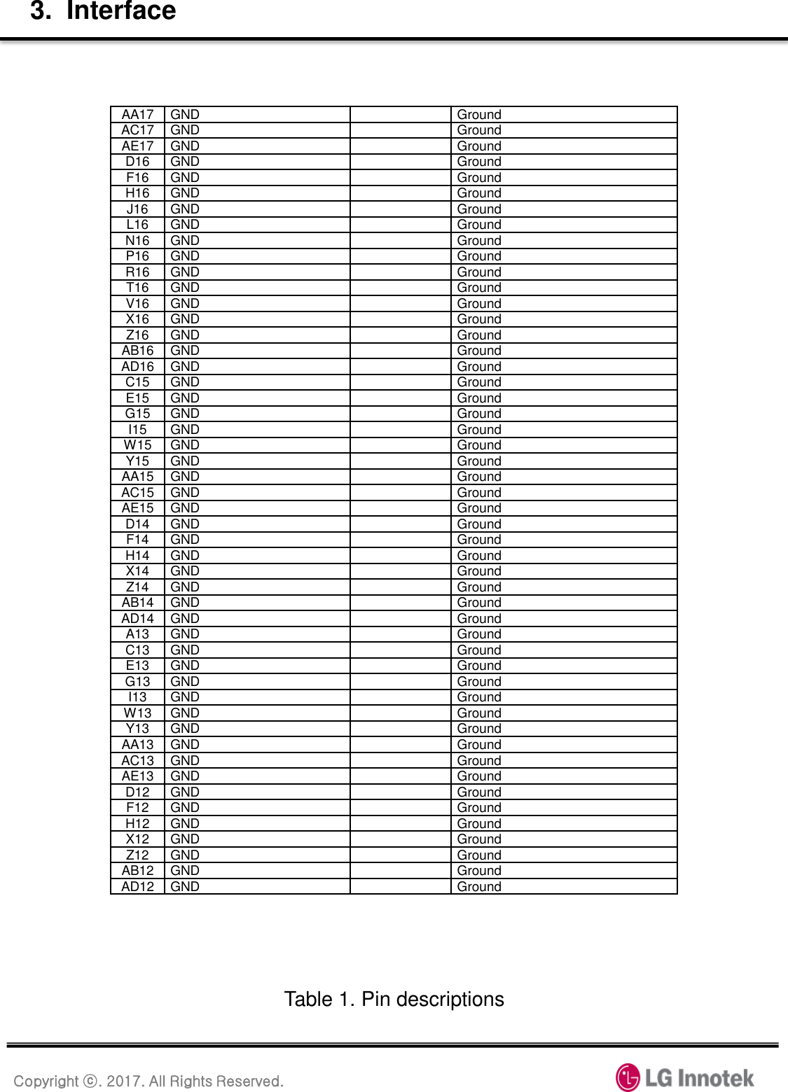
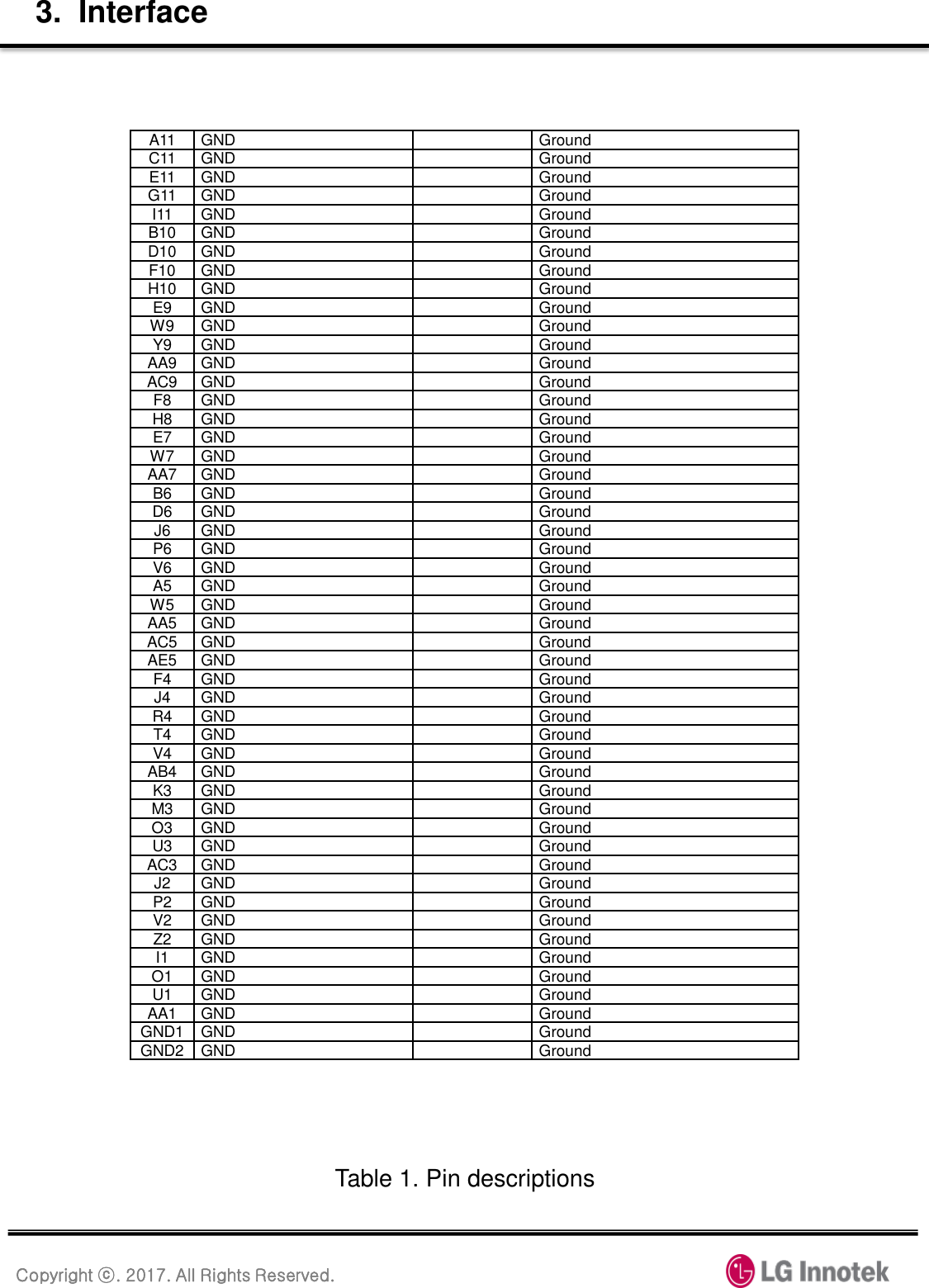
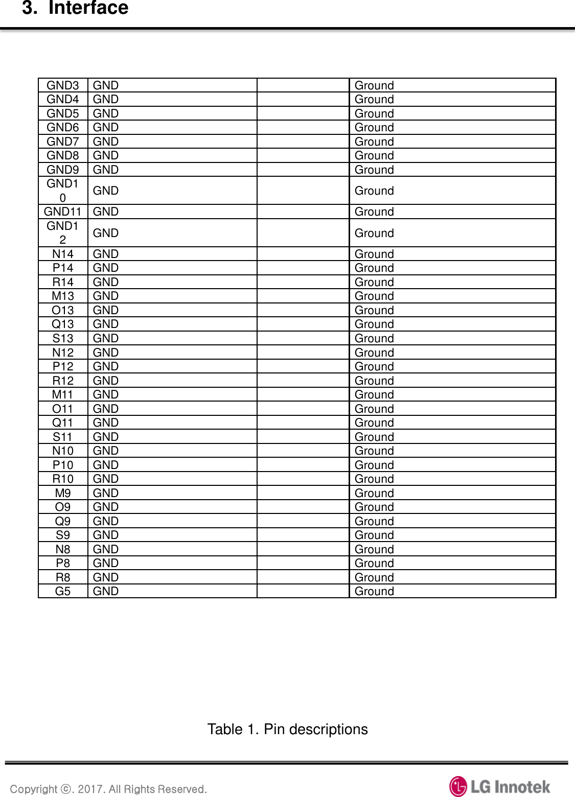
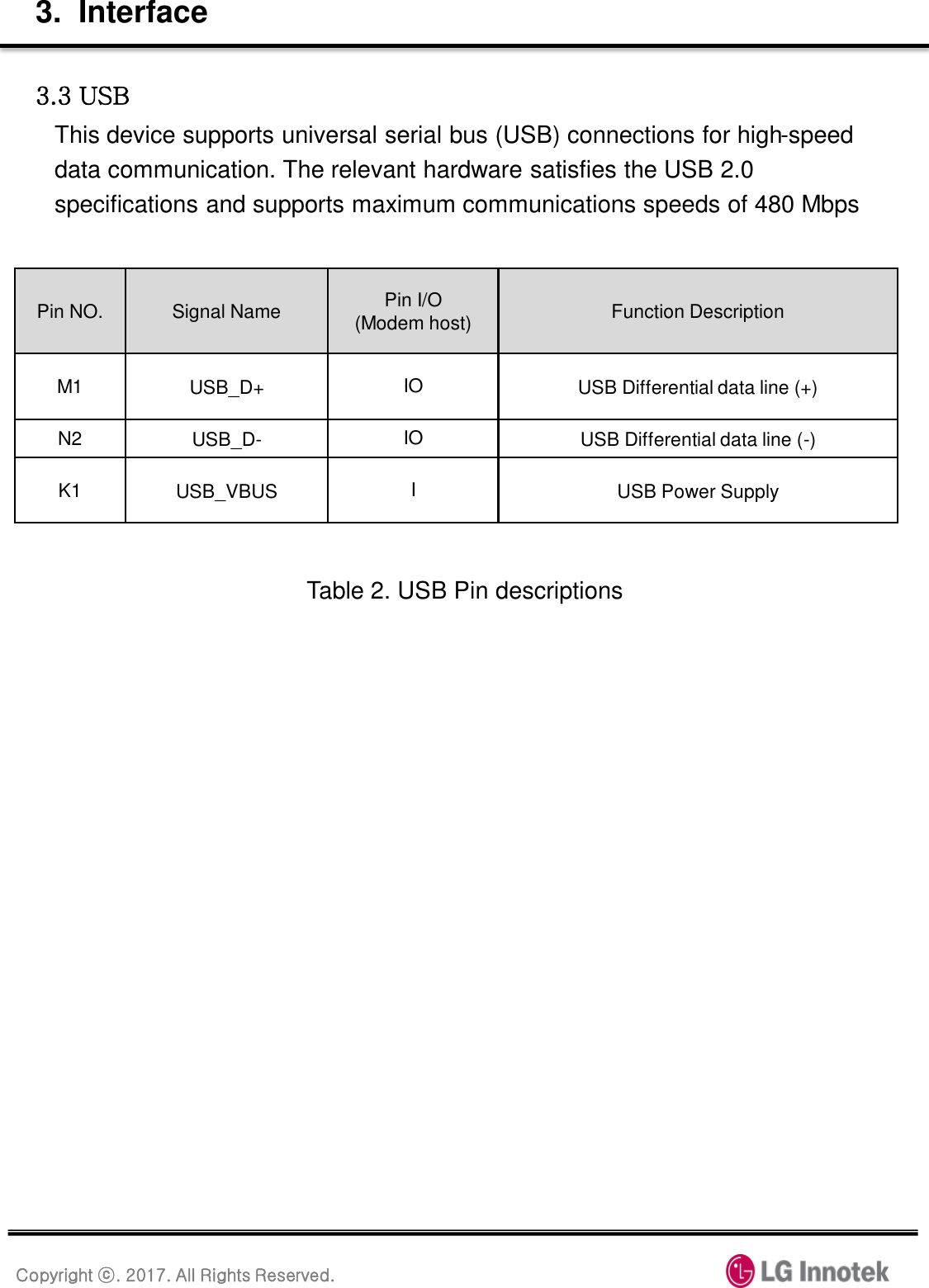
LG Innotek BK1000 Telematics Modem User Manual 1
LG Innotek Co., Ltd. Telematics Modem 1
UserManual.wiki
>
LG Innotek
>
BK1000 User Manual
User Manual
Navigation menu
Upload a User Manual
Namespaces
Wiki Guide
HTML
PDF
Info
Views
User Manual
Discussion / Help
Navigation


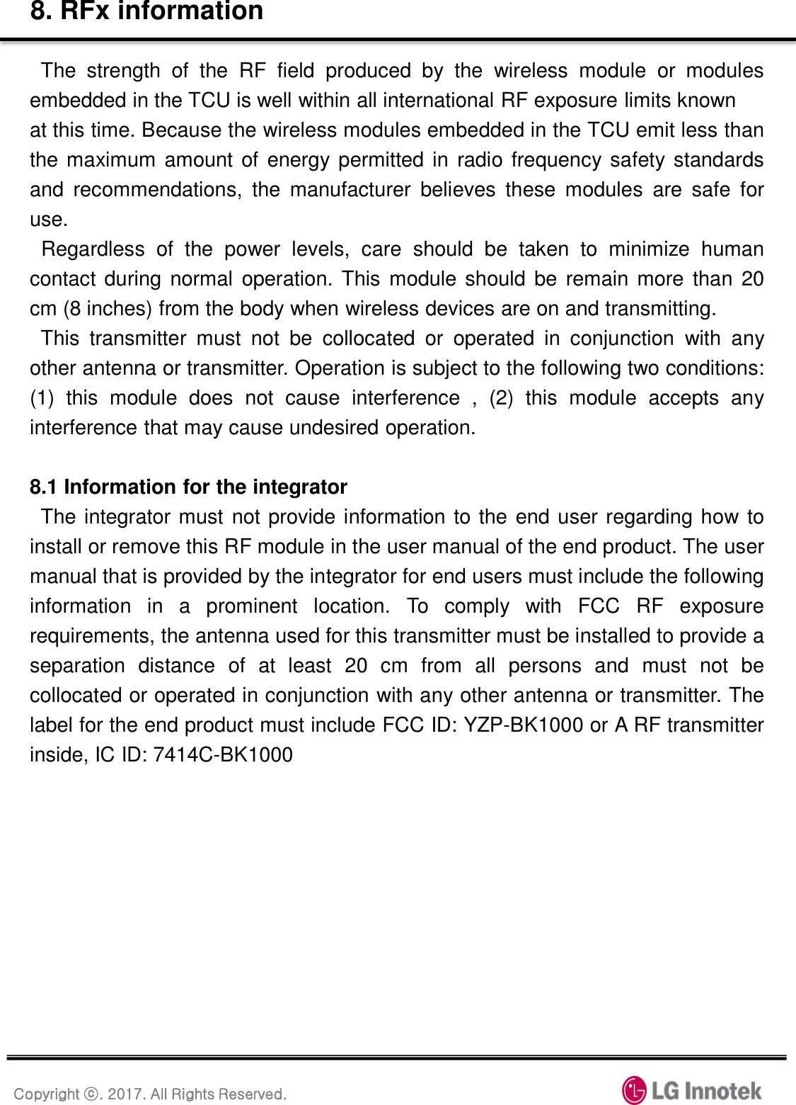
![Copyright ⓒ. 2017. All Rights Reserved. 9. Approbation FCCThis module complies with FCC/IC rules. FCC : Part 22, Part 24, Part 27IC : RSS-130, RSS-132, RSS-133, RSS-139Furthermore, this device complies with FCC/IC radiation exposure limits set forth for uncontrolled environments. This module must be installed and operated with minimum distance of 20 cm between the radiating element and the user. This module must not be co-located with any other transmitters or antennasCet module est conforme à l'exposition de FCC et IC rayonnements limites é-tablies pour un environnement non contrôlé. Cet module doit être installé et utilisé avec une distance minimale de 20 cm entre le radiateur et votre corps. Ce module ne doit pas être même endroit avec d'autres émetteur ou antennes.To comply with FCC/IC regulations limiting both the maximum RF output power and human exposure to RF radiation, the maximum antenna gain including cable loss in a mobile-only exposure condition must not exceed the values listed in the following table. To satisfy the FCC’s exterior labeling requirements, the following text must appear on the exterior of the end product. Contains transmitter module FCC ID: YZP-BK1000 Contains transmitter module IC ID: 7414C-BK1000 Changes or modifications to this equipment may cause harmful interference unless the modifications are expressly approved in the instruction manual. Users may lose the authority to operate this equipment if an unauthorized change or codification is made. Note: If this module is intended for use in a portable device, additional testing will be required to satisfy the RF exposure and SAR requirements of FCC Part 2.1093 and RSS-102. Band Frequency Range [MHz] Maximum Antenna Gain[dBi] WCDMA(B5) 826.40~846.6 4.5 WCDMA(B2) 1852.4~1907.6 2.0 LTE(B2) 1850~1910 2.0 LTE(B4) 1710~1755 2.0 LTE(B5) 824~849 4.5 LTE(B17) 704~716 4.5](https://usermanual.wiki/LG-Innotek/BK1000/User-Guide-3364912-Page-27.png)