LG Innotek BK1000 Telematics Modem User Manual 1
LG Innotek Co., Ltd. Telematics Modem 1
User Manual

Copyright ⓒ. 2017. All Rights Reserved.
User Guide for the LTD-BK1000
1. Overview
2. Major features
3. Interface
4. Electrical specifications
5. RF specifications
6. Mechanical specifications
7. General specifications
8. Connectors
9. RFx information
10. Approbation FCC
Table of Contents
Product: LTE_WCDMA Wireless Modem
Model name: LTD-BK1000

Copyright ⓒ. 2017. All Rights Reserved.
The LTD-BK1000 is a personal mobile communication device that incorporates
the latest compact radio technology, including smaller and lighter components
and support for WCDMA(850/1900MHz) bands and LTE(700/850/1700/1900
MHz). This device acts as the vehicle’s telematics system and connects to
WCDMA (HSPA+) and LTE wireless networks and wireless modules to allow
voice and data communication. Furthermore, this device can operate on land
and water as well as other similar areas.
In LTE mode, the device provides uplink speeds of up to 50 Mbps and
downlink speeds of up to 150 Mbps for seamless transfer of data such as
movies and video calls. The device also supports the transfer of large amounts
of data.
The device communicates with the host system via a standard RS-232 or USB
port, and AT commands and control commands can be used to send data. Voice
calls are also possible.
1. Overview
Copyright ⓒ. 2017. All Rights Reserved.
Mechanical
Dimensions
34 x 40 x 3.5 mm
(L x W x T)
(Tolerance
– width, length : TBD)
Weight
TBD g (max)
Interface
USB, general purpose I/O pins
Temperature*
Operation: -20 ℃ - +70 ℃
Storage: -40 ℃ - +85 ℃
Technology
Main chipset
MDM9628
Memory
4Gb(NAND) / 1Gb(SDRAM)
Standard
WCDMA (HSPA+)
- DL Speed : 14.4 Mbps
- UL Speed : 5.76 Mbps
LTE
- DL Speed : 150 Mbps
- UL Speed : 50 Mbps
Band
WCDMA B2, B5
LTE B2, B4, B5, B17
Power
WCDMA : Typ. 24dBm (Power Class 3)
LTE : Typ. 23dBm (Power Class 3)
ETC
DC power
4 V
Functions
Voice, data, SMS
2. Major features
Copyright ⓒ. 2017. All Rights Reserved.
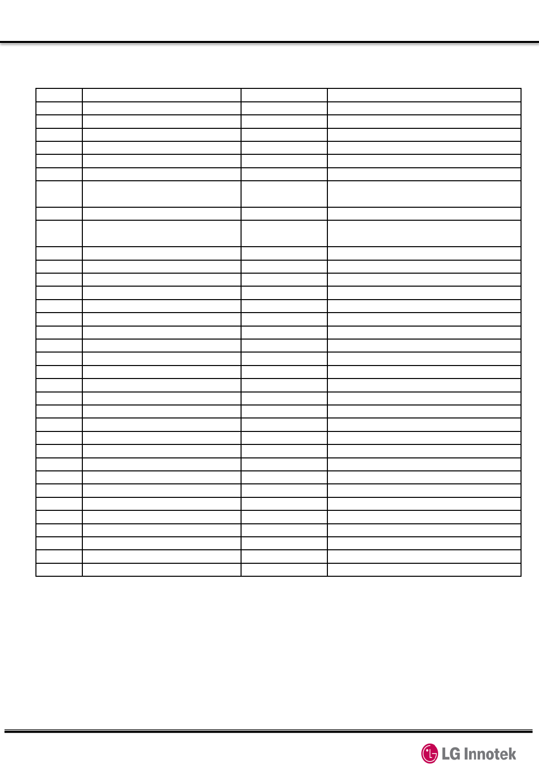
3. Interface
3.1 LGA Pad Layout (Top View)
Figure 1. LGA Pin map
GND12 GND10 GND6 GND5
GND GND GND GND
GND GND
GND11 GND4
21 A21 C21 E21 G21 I21 K21 M21 O21 Q21 S21 U21 W21 Y21 AA21 AC21 AE21
GND MAIN_ANT GND GND GND GND GND GND GND GND GND GND GND GND ANT_DIV GND
20 B20 D20 F20 H20 J20 L20 N20 P20 R20 T20 V20 X20 Z20 AB20 AD20
GND GND MAIN_ANT_DTC_EN GND GND GND GND GND GND GND GND GND DIV_ANT_DTC_EN GND GND
19 A19 C19 E19 G19 I19 K19 M19 O19 Q19 S19 U19 W19 Y19 AA19 AC19 AE19
GND GND ADC1 GND GND GND GND GND GND GND GND GND GND ADC2 GND GND
18 B18 D18 F18 H18 J18 L18 N18 P18 R18 T18 V18 X18 Z18 AB18 AD18
GND GND GND GND GND GND GND GND GND GND GND GND GND GND GND
17 A17 C17 E17 G17 I17 K17 M17 O17 Q17 S17 U17 W17 Y17 AA17 AC17 AE17
VPH_PWR GND GND GND GND GND GND GND GND GND GND GND GND GND GND GND
16 B16 D16 F16 H16 J16 L16 N16 P16 R16 T16 V16 X16 Z16 AB16 AD16
VPH_PWR GND GND GND GND GND GND GND GND GND GND GND GND GND GND
15 A15 C15 E15 G15 I15 W15 Y15 AA15 AC15 AE15
VPH_PWR GND GND GND GND GND GND GND GND GND
14 B14 D14 F14 H14 N14 P14 R14 X14 Z14 AB14 AD14
VPH_PWR GND GND GND GND GND GND GND GND GND GND
13 A13 C13 E13 G13 I13 M13 O13 Q13 S13 W13 Y13 AA13 AC13 AE13
GND GND GND GND GND GND GND GND GND GND GND GND GND GND
12 B12 D12 F12 H12 N12 P12 R12 X12 Z12 AB12 AD12
NC GND GND GND GND GND GND GND GND GND GND
11 A11 C11 E11 G11 I11 M11 O11 Q11 S11 W11 Y11 AA11 AC11 AE11
GND GND GND GND GND GND GND GND GND SGMII_RX_M SGMII_TX_P EPHY_RST_N SGMII_CLK EPHY_INT_N
10 B10 D10 F10 H10 N10 P10 R10 X10 Z10 AB10 AD10
GND GND GND GND GND GND GND SGMII_RX_P SGMII_TX_M SGMII_DATA GND
9A9 C9 E9 G9 I9 M9 O9 Q9 S9 W9 Y9 AA9 AC9 AE9
VPH_PWR VREG_L11_1P8 GND NC NC GND GND GND GND GND GND GND GND MDM_JTAG_SRST_N
8B8 D8 F8 H8 N8 P8 R8 X8 Z8 AB8 AD8
VPH_PWR VREG_L11_1P8 GND GND GND GND GND MDM2AP_INT_N AP2MDM_INT_N MDM_JTAG_TCK MDM_JTAG_PS_HOLD
7A7 C7 E7 G7 I7 W7 Y7 AA7 AC7 AE7
VPH_PWR VPH_PWR GND NC SPI_LEVEL_SHIFT_EN GND COEX_UART_RX GND MDM_JTAG_TMS MDM_JTAG_TRST_N
6B6 D6 F6 H6 J6 L6 N6 P6 R6 T6 V6 X6 Z6 AB6 AD6
GND GND GPIO ACC_PWR_ON GND GPIO GPIO GND SPI_CS_N SPI_CLK GND DSRC_SLP_CLK COEX_UART_TX MDM_JTAG_TDO MDM_JTAG_TDI
5A5 C5 E5 G5 I5 K5 M5 O5 Q5 S5 U5 W5 Y5 AA5 AC5 AE5
GND NC GPIO GND BOOT_OK UART1_TX UART2_TX UART3_TX SPI_INTERRUPT SPI_MOSI SPI_MISO GND
WLAN_3V_EN_DSRC
GND GND GND
4B4 D4 F4 H4 J4 L4 N4 P4 R4 T4 V4 X4 Z4 AB4 AD4
MDM_RESOUT_N NC GND MGS GND UART1_RX UART2_RX UART3_RX GND GND GND RFCLK2_QCA DSRC_PPS GND Ehernet_DC-DC_EN
3A3 C3 E3 G3 I3 K3 M3 O3 Q3 S3 U3 W3 Y3 AA3 AC3 AE3
PHONE_ON_N LGA_RESIN_N GND 96H_END UIM1_PRESENT GND GND GND SDC_DATA3 SDC_DATA2 GND PCM_EN PCM_DIN WLAN_EN_DSRC GND VREG_L5_UIM2
2B2 D2 F2 H2 J2 L2 N2 P2 R2 T2 V2 X2 Z2 AB2 AD2
GND GND VREG_L6_UIM1 UIM1_CLK GND USB_ID USB_HS_DM GND SDC_DATA1 SDC_DATA0 GND PCM_CLK GND HSIC_DATA NC
1A1 C1 E1 G1 I1 K1 M1 O1 Q1 S1 U1 W1 Y1 AA1 AC1 AE1
GND GND UIM1_RESET UIM1_DATA GND USB_VBUS USB_HS_DP GND SDC_CMD SDC_CLK GND PCM_SYNC PCM_DOUT GND HSIC_STB NC
GND9 A B C D E F G H I J K L M N O P Q R S T U V W X Y Z AA AB AC AD AE GND2
GND GND
GND GND GND GND
GND8 GND7 GND3 GND1
Copyright ⓒ. 2017. All Rights Reserved.
3. Interface
3.2 Pin description
Table 1. Pin descriptions
PAD
.
NAME
DIRECTION
DESCRIPTION
Antenna Interface Pads
C21
MAIN_ANT
Input/Output
RF Main Antenna
AC21
DIV_ANT
Input/Output
RF Diversity Antenna
User Interface Pads
H6
ACC_PWR_ON
Input
ACC_PWR_ON
I5
BOOT_OK
Output
BOOT_OK
H4
MSG
Output
MSG
G3
96H_END
Output
96H_END
F20
MAIN_ANT_DTC_EN
Output
Main ANT Detect Enable
Z20
DIV_ANT_DTC_EN
Output
Diversity ANT Detect Enable
I7
SPI_LEVEL_SHIFT_EN
Output
SPI LEVEL SHIFT Enable
AD4
ETHERNET_DCDC_ENABLE
Output
Ethernet power enable
F6
GPIO1
Input/Output
(Do not use
with External
PU)
General purpose I/O
E5
GPIO2
General purpose I/O
L6
GPIO3
Input/Output
(Not
support INTERR
UPT)
General purpose I/O
N6
GPIO4
General purpose I/O
ADC Interface Pads
E19
ADC1
Input
ADC Convertor input for main
antenna detect
AA19
ADC2
Input
ADC Convertor input for diversity
antenna detect
PCM Interface Pads
W3
PCM_EN
Output
PCM 3.3 Level Shifter Enable
X2
PCM_CLK
Input
PCM Clock
W1
PCM_SYNC
Input
PCM Frame Sync
Y3
PCM_DIN
Input
PCM Data In
Y1
PCM_DOUT
Output
PCM Data Out
JTAG Pin Description
AC7
MDM_JTAG_TMS
Input/Output
JTAG mode select input
AD8
MDM_JTAG_PS_HOLD
input
JTAG PS HOLD detect
AD6
MDM_JTAG_TDI
Input
JTAG data input
AE7
MDM_JTAG_TRST_N
Input
JTAG reset for debug
AB6
MDM_JTAG_TDO
Output
JTAG debugging
AB8
MDM_JTAG_TCK
Input
JTAG clock input
AE9
MDM_JTAG_SRST_N
Input
JTAG reset
USB Interface Pads
N2
USB_HS_DM
Input/Output
USB high speed data (minus)
M1
USB_HS_DP
Input/Output
USB high speed data (plus)
K1
USB_VBUS
Input
USB power
L2
USB_ID
Input
USB ID
SDIO Interface Pads
S1
SDC_CLK
Output
Secure digital controller clock
Q1
SDC_CMD
Output
Secure digital controller command
T2
SDC_DATA0
Input/Output
Secure digital controller data bit 0
R2
SDC_DATA1
Input/Output
Secure digital controller data bit 1
S3
SDC_DATA2
Input/Output
Secure digital controller data bit 2
Copyright ⓒ. 2017. All Rights Reserved.
3. Interface
Table 1. Pin descriptions
Q3
SDC_DATA3
Input/Output
Secure digital controller data bit 3
SGMMI Interface Pads
AA11
EPHY_RST_N or UIM2_RESET
Output
Ethernet PHY reset
AE11
EPHY_INT_N or UIM2_DETECT
Input
Ethernet PHY interrupt
AB10
SGMII_DATA or UIM2_CLK
Input/Output
SGMII input Output data
AD10
GND
Ground
X10
SGMII_RX_P
Input
SGMII receive
- plus
W11
SGMII_RX_M
Input
SGMII receive
-minus
Z10
SGMII_TX_M
Output
SGMII transmit
- plus
Y11
SGMII_TX_P
Output
SGMII transmit
-minus
AC11
SGMII_CLK or UIM2_DATA
Output
SGMII clock
SPI Interface Pads
S5
SPI_MOSI
Output
SPI Serial Output
T6
SPI_CLK
Output
SPI Serial Clock
R6
SPI_CS_N
Output
SPI Chip Select
U5
SPI_MISO
Input
SPI Serial input
Q5
SPI_INTERRUPT
Input
MICOM → LGA SPI interrupt
UART Interface Pads
M5
UART2_TX
Output
UART2 Transmit data
N4
UART2_RX
Input
UART2 Receive data
K5
UART1_TX
Output
Debug UART5 Transmit Data
L4
UART1_RX
Input
Debug UART5 Receive Data
O5
UART3_TX
Output
UART6 Transmit data
P4
UART3_RX
Input
UART6 Receive data
USIM Interface Pads
I3
UIM1_PRESENT
Input
Detection of an external UIM card
H2
UIM1_CLK
Output
Clock Output to an external UIM card
E1
UIM1_RESET
Output
Reset Output to an external UIM card
G1
UIM1_DATA
Input/Output
Data connection with an external UIM
card
F2
VREG_L6_UIM1
Output
Supply Output for an external UIM card
E3
GND
Ground
D2
GND
Ground
A1
GND
Ground
C1
GND
Ground
B2
GND
Ground
HSIC Pin Description
AB2
HSIC_DATA
Input/Output
HSIC data
AC1
HSIC_STB
Input/Output
HSIC Strobe signal
AD2
NC
No Connect
AE1
NC
No Connect
DSRC Pin Description
Y7
COEX_UART_RX
Input
LTE receiver sync for coexistence with
UART
Z6
COEX_UART_TX
Output
LTE transmitter sync for coexistence
with UART
X4
RFCLK2_QCA
Output
Low noise RF clock Output
AA3
WLAN_EN_DSRC
Output
WLAN Enable
Copyright ⓒ. 2017. All Rights Reserved.
3. Interface
Table 1. Pin descriptions
X6
DSRC_SLP_CLK
Output
DSRC sleep clock
Y5
WLAN_3V_EN_DSRC
Output
Used for WLAN enable
Z4
DSRC_PPS
Input/Output
Pulse Per Second
X8
MDM2AP_INT_N
Output
MDM to AP interrupt, PCM_LDO_EN
Z8
AP2MDM_INT_N
Input
AP to MDM interrupt
Control Pads
A3
LGA_PHONE_ON
Input
ON/OFF Control
B4
MDM_RESOUT_N
Output
Reset Output
C3
LGA_RESIN_N
Input
External Reset Input
Power Supply Pads
A17
VPH_PWR for PAM
Input
power supply (4.0V)
B16
VPH_PWR for PAM
Input
power
supply (4.0V)
A15
VPH_PWR for PAM
Input
power
supply (4.0V)
B14
VPH_PWR for PAM
Input
power
supply (4.0V)
A9
VPH_PWR for PMIC
Input
power
supply (4.0V)
B8
VPH_PWR for PMIC
Input
power
supply (4.0V)
A7
VPH_PWR for PMIC
Input
power
supply (4.0V)
C7
VPH_PWR for PMIC
Input
power
supply (4.0V)
Voltage Reference Pad
C9
VREG_L11_1P8
Output
LDO out for 1.8V pull up
D8
VREG_L11_1P8
Output
LDO out for 1.8V pull up
AE3
Voltage Reference for SGMII
(VREG_L5_UIM2)
–
Ethernet
IO
전압 level Output
Ethernet I/O voltage
NC Pads
G9
NC
No Connect
B12
NC
No Connect
I9
NC
No Connect
G7
NC
No Connect
C5
NC
No Connect
D4
NC
No Connect
A21
GND
Ground
E21
GND
Ground
G21
GND
Ground
I21
GND
Ground
K21
GND
Ground
M21
GND
Ground
O21
GND
Ground
Q21
GND
Ground
S21
GND
Ground
U21
GND
Ground
W21
GND
Ground
Y21
GND
Ground
AA21
GND
Ground
AE21
GND
Ground
B20
GND
Ground
D20
GND
Ground
H20
GND
Ground
J20
GND
Ground
Copyright ⓒ. 2017. All Rights Reserved.
3. Interface
Table 1. Pin descriptions
L20
GND
Ground
N20
GND
Ground
P20
GND
Ground
R20
GND
Ground
T20
GND
Ground
V20
GND
Ground
X20
GND
Ground
AB20
GND
Ground
AD20
GND
Ground
A19
GND
Ground
C19
GND
Ground
G19
GND
Ground
I19
GND
Ground
K19
GND
Ground
M19
GND
Ground
O19
GND
Ground
Q19
GND
Ground
S19
GND
Ground
U19
GND
Ground
W19
GND
Ground
Y19
GND
Ground
AC19
GND
Ground
AE19
GND
Ground
B18
GND
Ground
D18
GND
Ground
F18
GND
Ground
H18
GND
Ground
J18
GND
Ground
L18
GND
Ground
N18
GND
Ground
P18
GND
Ground
R18
GND
Ground
T18
GND
Ground
V18
GND
Ground
X18
GND
Ground
Z18
GND
Ground
AB18
GND
Ground
AD18
GND
Ground
C17
GND
Ground
E17
GND
Ground
G17
GND
Ground
I17
GND
Ground
K17
GND
Ground
M17
GND
Ground
O17
GND
Ground
Q17
GND
Ground
S17
GND
Ground
U17
GND
Ground
W17
GND
Ground
Y17
GND
Ground
Copyright ⓒ. 2017. All Rights Reserved.
3. Interface
Table 1. Pin descriptions
AA17
GND
Ground
AC17
GND
Ground
AE17
GND
Ground
D16
GND
Ground
F16
GND
Ground
H16
GND
Ground
J16
GND
Ground
L16
GND
Ground
N16
GND
Ground
P16
GND
Ground
R16
GND
Ground
T16
GND
Ground
V16
GND
Ground
X16
GND
Ground
Z16
GND
Ground
AB16
GND
Ground
AD16
GND
Ground
C15
GND
Ground
E15
GND
Ground
G15
GND
Ground
I15
GND
Ground
W15
GND
Ground
Y15
GND
Ground
AA15
GND
Ground
AC15
GND
Ground
AE15
GND
Ground
D14
GND
Ground
F14
GND
Ground
H14
GND
Ground
X14
GND
Ground
Z14
GND
Ground
AB14
GND
Ground
AD14
GND
Ground
A13
GND
Ground
C13
GND
Ground
E13
GND
Ground
G13
GND
Ground
I13
GND
Ground
W13
GND
Ground
Y13
GND
Ground
AA13
GND
Ground
AC13
GND
Ground
AE13
GND
Ground
D12
GND
Ground
F12
GND
Ground
H12
GND
Ground
X12
GND
Ground
Z12
GND
Ground
AB12
GND
Ground
AD12
GND
Ground
Copyright ⓒ. 2017. All Rights Reserved.
3. Interface
Table 1. Pin descriptions
A11
GND
Ground
C11
GND
Ground
E11
GND
Ground
G11
GND
Ground
I11
GND
Ground
B10
GND
Ground
D10
GND
Ground
F10
GND
Ground
H10
GND
Ground
E9
GND
Ground
W9
GND
Ground
Y9
GND
Ground
AA9
GND
Ground
AC9
GND
Ground
F8
GND
Ground
H8
GND
Ground
E7
GND
Ground
W7
GND
Ground
AA7
GND
Ground
B6
GND
Ground
D6
GND
Ground
J6
GND
Ground
P6
GND
Ground
V6
GND
Ground
A5
GND
Ground
W5
GND
Ground
AA5
GND
Ground
AC5
GND
Ground
AE5
GND
Ground
F4
GND
Ground
J4
GND
Ground
R4
GND
Ground
T4
GND
Ground
V4
GND
Ground
AB4
GND
Ground
K3
GND
Ground
M3
GND
Ground
O3
GND
Ground
U3
GND
Ground
AC3
GND
Ground
J2
GND
Ground
P2
GND
Ground
V2
GND
Ground
Z2
GND
Ground
I1
GND
Ground
O1
GND
Ground
U1
GND
Ground
AA1
GND
Ground
GND1
GND
Ground
GND2
GND
Ground
Copyright ⓒ. 2017. All Rights Reserved.
3. Interface
Table 1. Pin descriptions
GND3
GND
Ground
GND4
GND
Ground
GND5
GND
Ground
GND6
GND
Ground
GND7
GND
Ground
GND8
GND
Ground
GND9
GND
Ground
GND1
0
GND
Ground
GND11
GND
Ground
GND1
2
GND
Ground
N14
GND
Ground
P14
GND
Ground
R14
GND
Ground
M13
GND
Ground
O13
GND
Ground
Q13
GND
Ground
S13
GND
Ground
N12
GND
Ground
P12
GND
Ground
R12
GND
Ground
M11
GND
Ground
O11
GND
Ground
Q11
GND
Ground
S11
GND
Ground
N10
GND
Ground
P10
GND
Ground
R10
GND
Ground
M9
GND
Ground
O9
GND
Ground
Q9
GND
Ground
S9
GND
Ground
N8
GND
Ground
P8
GND
Ground
R8
GND
Ground
G5
GND
Ground
Copyright ⓒ. 2017. All Rights Reserved.
3. Interface
3.3 USB
This device supports universal serial bus (USB) connections for high-speed
data communication. The relevant hardware satisfies the USB 2.0
specifications and supports maximum communications speeds of 480 Mbps
Table 2. USB Pin descriptions
Pin NO. Signal Name Pin I/O
(Modem host) Function Description
M1 USB_D+ IO USB Differential data line (+)
N2 USB_D- IO USB Differential data line (-)
K1 USB_VBUS I USB Power Supply
Copyright ⓒ. 2017. All Rights Reserved.
3. Interface
3.4 Audio
This module includes a PCM interface. The pull-up and pull-down resistors
attached to these pin must provide more than 50 Kohm of resistance.
Table 3. PCM Pin descriptions
3.5 User interface
Pin
No.
Signal Name Direction
Function
I5 BOOT_OK O Indicates that the Modem boot is complete.
C3 RESET_IN I Control line to unconditionally restart the
module.
H4 MSG O Indicates that the Modem receive Urgent
message.
G3 96H_END O Indicates that the 96hr sleep mode is end.
H6 ACC_ON_SLEEP
I Control line to power on or 96hr sleep mode.
A3 Phone_ON I Control line to power on / off
Table 4. User interface Pin descriptions
Pin NO.
Signal Name Pin I/O
(Modem host) Function Description
W1 PCM_SYNC
I PCM Interface sync
X2 PCM_CLK
I PCM Interface clock
Y1 PCM_TXD
O PCM Interface digital audio data out
Y3 PCM_RXD I PCM Interface digital audio data in
Copyright ⓒ. 2017. All Rights Reserved.
4. Electrical specifications
4.1 Power supply specifications
The host system provides the power supply (V_BATT)DC 4 V, 2.5 A to the
device. The internal power supply module manages the power supplied to the
integral circuits and maintains constant voltages. This module also controls
each power block to minimize power consumption.
In particular, the PAM (power amplifier module) consumes a lot of power, so it
receives a direct power supply of 4 V from the V_BATT. Therefore the
V_BATT signal inputs only the supply power of the PAM, even when the
absolute rating is higher. In addition, the entire power input module blocks and
protects against high surges and ESD in the NAD module.
Pin No. Signal Name
Direction
MIN TYP MAX
A7,C7,B8,A9,
B14,A15,B16,
A17
V_BATT I 3.9 V 4 V 4.1 V
Table 5. Power supply specifications

Copyright ⓒ. 2017. All Rights Reserved.
4. Electrical specifications
4.2 Logic level specifications
4.2.1 Digital logic level specifications
Table 6. Digital logic level specifications
Signal Name Type Low High Unit
Min Max Min Max
BOOT_OK O 0 0.45 1.35 1.8
V
RESET_IN I -0.3 0.63 1.17 1.8
MSG O 0 0.45 1.35 1.8
96H_END O 0 0.45 1.35 1.8
ACC_ON_SLEEP
I 0 0.63 1.17 1.8

Copyright ⓒ. 2017. All Rights Reserved.
5. RF specifications
5.1 WCDMA
5.1.1 Receiver
.- Bandwidth : 5MHz
.- Frequency : 869MHz – 894MHz (B5), 1930MHz – 1990MHz (B2)
.- RF to Baseband Direct conversion (Zero IF)
.- Modulation method : QPSK, 16QAM
.- Sensitivity : ≤-104dBm (BER = Under 0.1%)
5.1.2 Transmitter
.- Frequency: 824MHz – 849MHz (B5), 1850MHz – 1910MHz (B2)
.- Maximum RF Output : Power class3 , 20.3dBm ~ 25.7dBm
.- Modulation method : QPSK
.- Baseband to RF Direct conversion (Zero IF)
5.2 LTE
5.2.1 Receiver
.- Bandwidth :
B2/B4(5 MHz, 10 MHz, 15 MHz, 20 MHz), B5/B17(5 MHz, 10 MHz)
.- Frequency :
B2 (1930 MHz – 1990 MHz), B4 (2110 MHz – 2155 MHz), B5 (869 MHz
– 894 MHz), B17 (734 MHz – 746 MHz)
.- RF to Baseband Direct conversion (Zero IF)
.- Modulation method : QPSK, 16QAM and 64QAM
.- Sensitivity :
B2 (≤-94.3dBm @QPSK, BW:10 MHz), B4 (≤-96.3dBm @QPSK, BW:10
MHz), B5 (≤-94.3dBm @QPSK, BW:10 MHz), B17 (≤-93.3dBm
@QPSK, BW:10 MHz)

Copyright ⓒ. 2017. All Rights Reserved.
5. RF specifications
5.2.2 Transmitter
.- Frequency:
B2 (1850 MHz – 1910 MHz), B4 (1710 MHz – 1755 MHz),B5 (824 MHz
– 849 MHz), B17 (704 MHz – 716MHz)
.- Maximum RF Output : Power class3 , 20.3dBm ~ 25.7dBm
.- Modulation method : QPSK and 16QAM
.- Baseband to RF Direct conversion (Zero IF)

Copyright ⓒ. 2017. All Rights Reserved.
6. Mechanical specifications
6.1 Environment specifications
.- Storage temp.: -40 ℃ - +85 ℃
.- Operating temp.: -20 ℃ - +70 ℃
(-20 ℃ - +70 ℃ : 3GPP specifications are satisfied
-30 ℃ - -20 ℃, +70 ℃ - +80 ℃ : May cause performance degradation)
.- Operating humidity: 80% (60℃) relative humidity
Copyright ⓒ. 2017. All Rights Reserved.
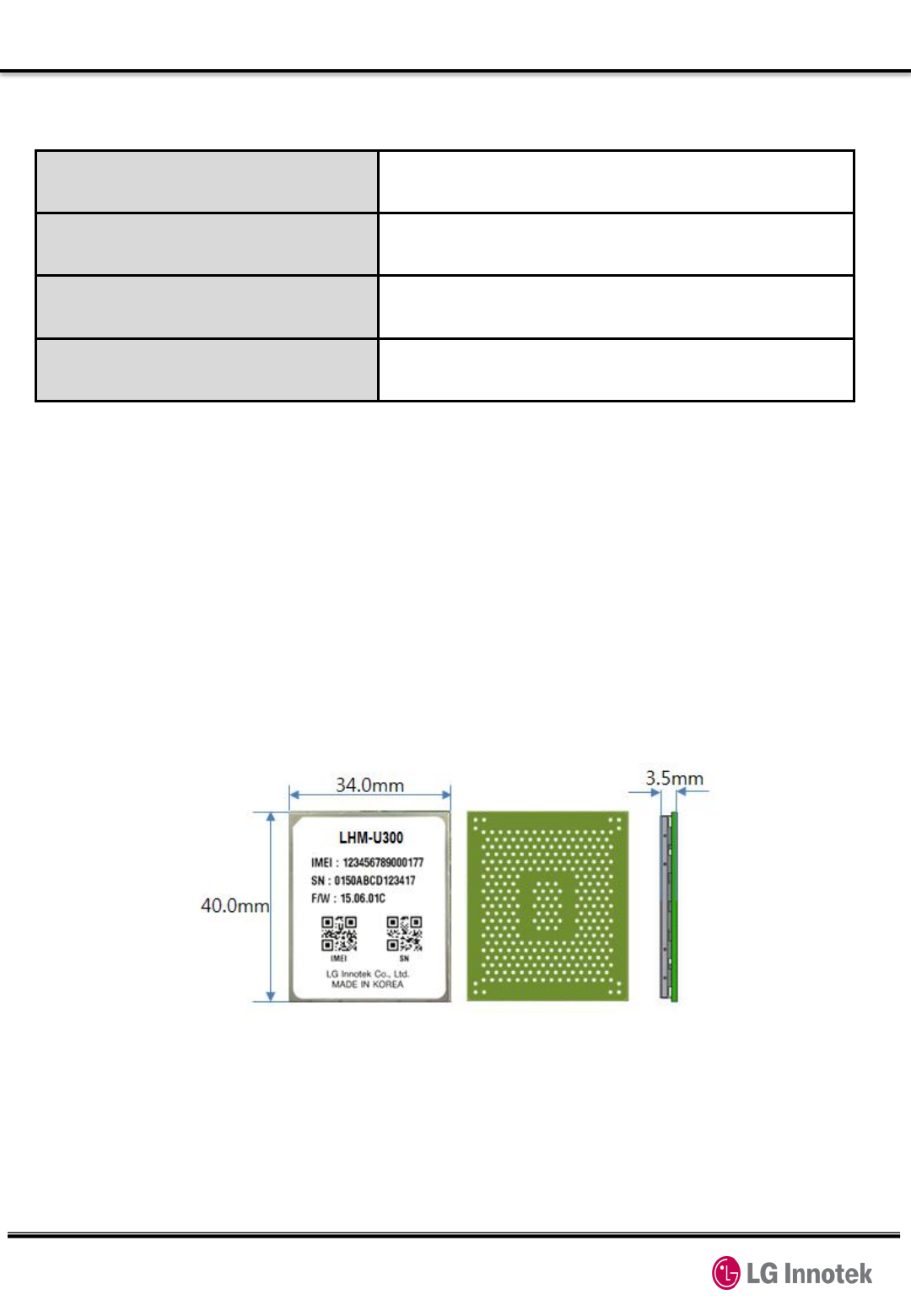
6. Mechanical specifications
6.1 Mechanical dimensions
Dimensions 34 x 40.0 x 3.5 mm (L x W x T)
(Tolerance – width, length : TBD)
Weight TBD grams(max.)
Modem interface connector 12709HS-H40 (Manufacture vendor : YUNHO)
Modem antenna Connector (Plug) KR15005-DD , KR15005-DG
(Manufacture vendor : KET)
Table 7. Mechanical specification
Figure 2. Mechanical dimension
Copyright ⓒ. 2017. All Rights Reserved.
7. General specifications
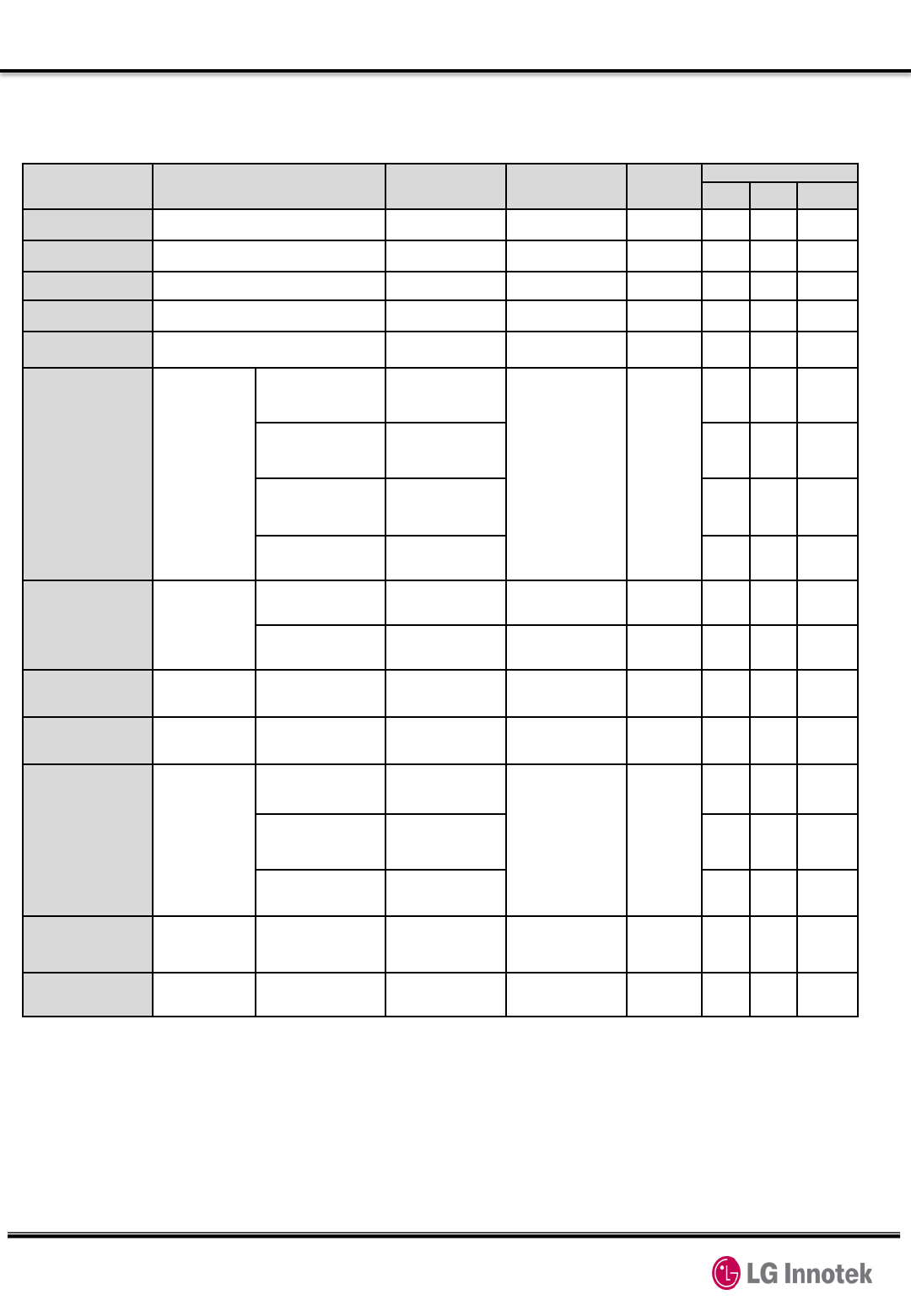
7.1 WCDMA B5 electrical specifications
Table 8. WCDMA B5 RF specification
TEST ITEM Spec. Test Temperature Test Freq
uency
CHANNEL
4357 4400 4458
1 Maximum Output Power 20.3~25.7dBm Normal, Temp L, Te
mp H Low, Mid,
High PASS
PASS
PASS
2 Frequency Error -195 ~ +195Hz Normal, Temp L, Te
mp H Low, Mid,
High PASS
PASS
PASS
3 Inner Loop Power Control in the Uplin
k PASS Normal Mid - PASS
-
4 Minimum Output Power -49dBm ↓ Normal, Temp L, Te
mp H Low, Mid,
High PASS
PASS
PASS
5 Occupied Bandwidth (OBW) 5MHz ↓ Normal Low, Mid,
High PASS
PASS
PASS
6 Spectrum emis
sion mask
SEM Band1 Offset2.
5-3.5MHz (at Freq+3.
5MHz) -48.5dBc ↓
Normal Low, Mid,
High
PASS
PASS
PASS
SEM Band1 Offset3.
5-7.5MHz (at Freq+7.
5MHz) -37.5dBc ↓ PASS
PASS
PASS
SEM Band1 Offset7.
5-8.5MHz (at Freq+8.
5MHz) -47.5dBc ↓ PASS
PASS
PASS
SEM Band1 Offset8.
5-12.5MHz -47.5dBc ↓ PASS
PASS
PASS
7
Adjacent Chan
nel Leakage Po
wer Ratio (ACL
R)
ACLR Offset +5/-5M
Hz Rel -32.2dBc ↓ Normal, Temp L, Te
mp H Low, Mid,
High PASS
PASS
PASS
ACLR Offset +10/-10
MHz Rel -42.2dBc ↓ Normal, Temp L, Te
mp H Low, Mid,
High PASS
PASS
PASS
8 Error Vector M
agnitude(EVM)
EVM at Tx output po
wer 24dBm /-18dBm 17.5% ↓ Normal Low, Mid,
High PASS
PASS
PASS
9 Peak code do
main error PCDE at Tx output p
ower 24dBm/-18dBm
-14dB ↓ Normal Low, Mid,
High PASS
PASS
PASS
10 Phase Disconti
nuity
Phase Discontinuity
max EVM 17.5% ↓
Normal Mid
- PASS
-
Phase Discontinuity
max Frequency Error
-195~195Hz - PASS
-
Phase Discontinuity
max 1500Hz 36 degrees ↓ - PASS
-
11 Reference Sen
sitivity Level
Ref Sense Go/No Go
I^or=-104dBm/3.84M
Hz
BER 0.1% ↓ Normal, Temp L, Te
mp H Low, Mid,
High PASS
PASS
PASS
12 Maximum Inpu
t Level
Max Input Go/No Go
I^or=-25.7dBm/3.84M
Hz
BER 0.1% ↓ Normal Mid - PASS
-
Copyright ⓒ. 2017. All Rights Reserved.
7. General specifications
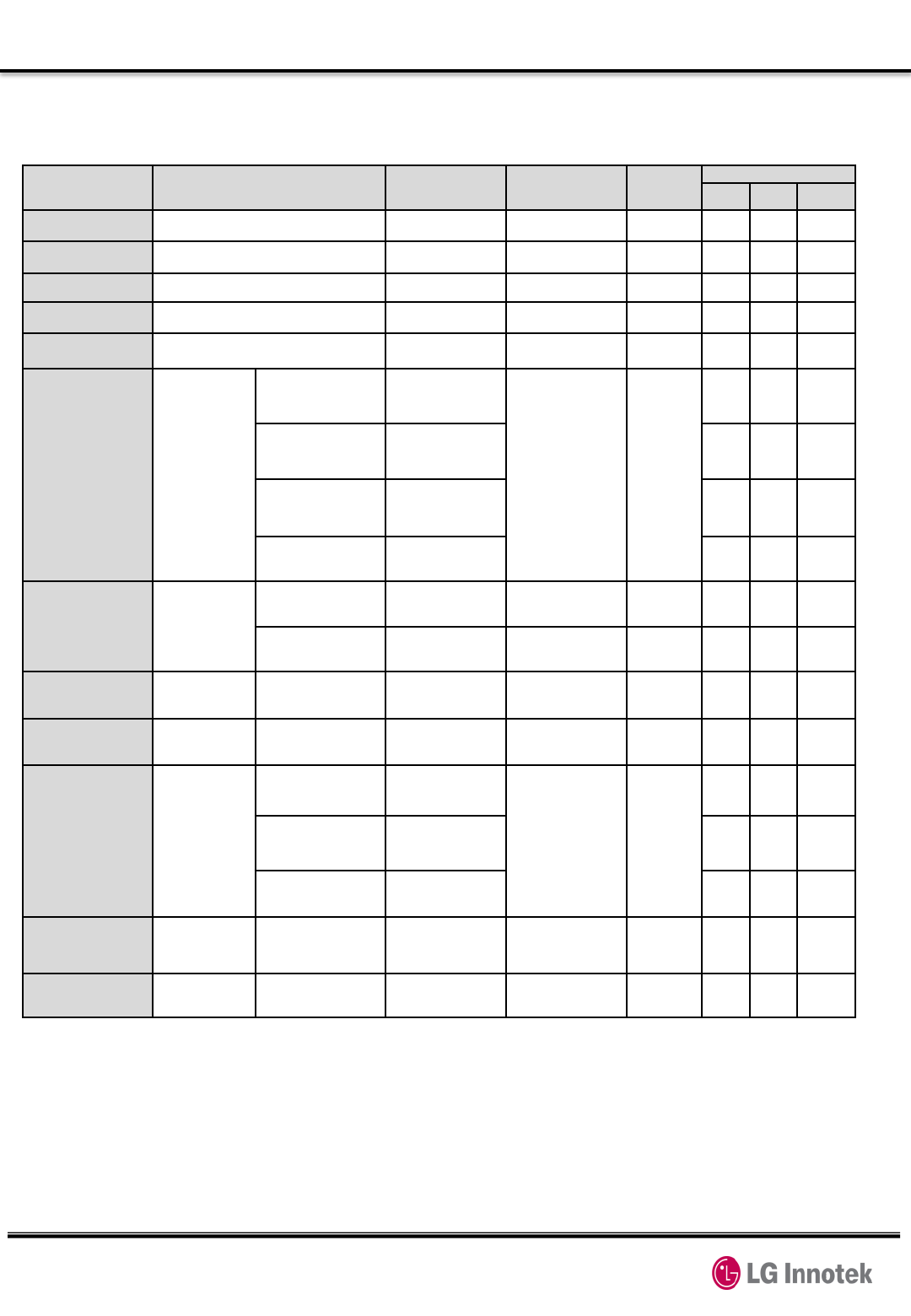
7.2 WCDMA B2 electrical specifications
Table 9. WCDMA B2 RF specification
TEST ITEM Spec. Test Temperature Test Freq
uency
CHANNEL
9662 9800 9938
1 Maximum Output Power 20.3~25.7dBm Normal, Temp L, Te
mp H Low, Mid,
High PASS
PASS
PASS
2 Frequency Error -195 ~ +195Hz Normal, Temp L, Te
mp H Low, Mid,
High PASS
PASS
PASS
3 Inner Loop Power Control in the Uplin
k PASS Normal Mid - PASS
-
4 Minimum Output Power -49dBm ↓ Normal, Temp L, Te
mp H Low, Mid,
High PASS
PASS
PASS
5 Occupied Bandwidth (OBW) 5MHz ↓ Normal Low, Mid,
High PASS
PASS
PASS
6 Spectrum emis
sion mask
SEM Band1 Offset2.
5-3.5MHz (at Freq+3.
5MHz) -48.5dBc ↓
Normal Low, Mid,
High
PASS
PASS
PASS
SEM Band1 Offset3.
5-7.5MHz (at Freq+7.
5MHz) -37.5dBc ↓ PASS
PASS
PASS
SEM Band1 Offset7.
5-8.5MHz (at Freq+8.
5MHz) -47.5dBc ↓ PASS
PASS
PASS
SEM Band1 Offset8.
5-12.5MHz -47.5dBc ↓ PASS
PASS
PASS
7
Adjacent Chan
nel Leakage Po
wer Ratio (ACL
R)
ACLR Offset +5/-5M
Hz Rel -32.2dBc ↓ Normal, Temp L, Te
mp H Low, Mid,
High PASS
PASS
PASS
ACLR Offset +10/-10
MHz Rel -42.2dBc ↓ Normal, Temp L, Te
mp H Low, Mid,
High PASS
PASS
PASS
8 Error Vector M
agnitude(EVM)
EVM at Tx output po
wer 24dBm /-18dBm 17.5% ↓ Normal Low, Mid,
High PASS
PASS
PASS
9 Peak code do
main error PCDE at Tx output p
ower 24dBm/-18dBm
-14dB ↓ Normal Low, Mid,
High PASS
PASS
PASS
10 Phase Disconti
nuity
Phase Discontinuity
max EVM 17.5% ↓
Normal Mid
- PASS
-
Phase Discontinuity
max Frequency Error
-195~195Hz - PASS
-
Phase Discontinuity
max 1500Hz 36 degrees ↓ - PASS
-
11 Reference Sen
sitivity Level
Ref Sense Go/No Go
I^or=-104dBm/3.84M
Hz
BER 0.1% ↓ Normal, Temp L, Te
mp H Low, Mid,
High PASS
PASS
PASS
12 Maximum Inpu
t Level
Max Input Go/No Go
I^or=-25.7dBm/3.84M
Hz
BER 0.1% ↓ Normal Mid - PASS
-

Copyright ⓒ. 2017. All Rights Reserved.
7. General specifications
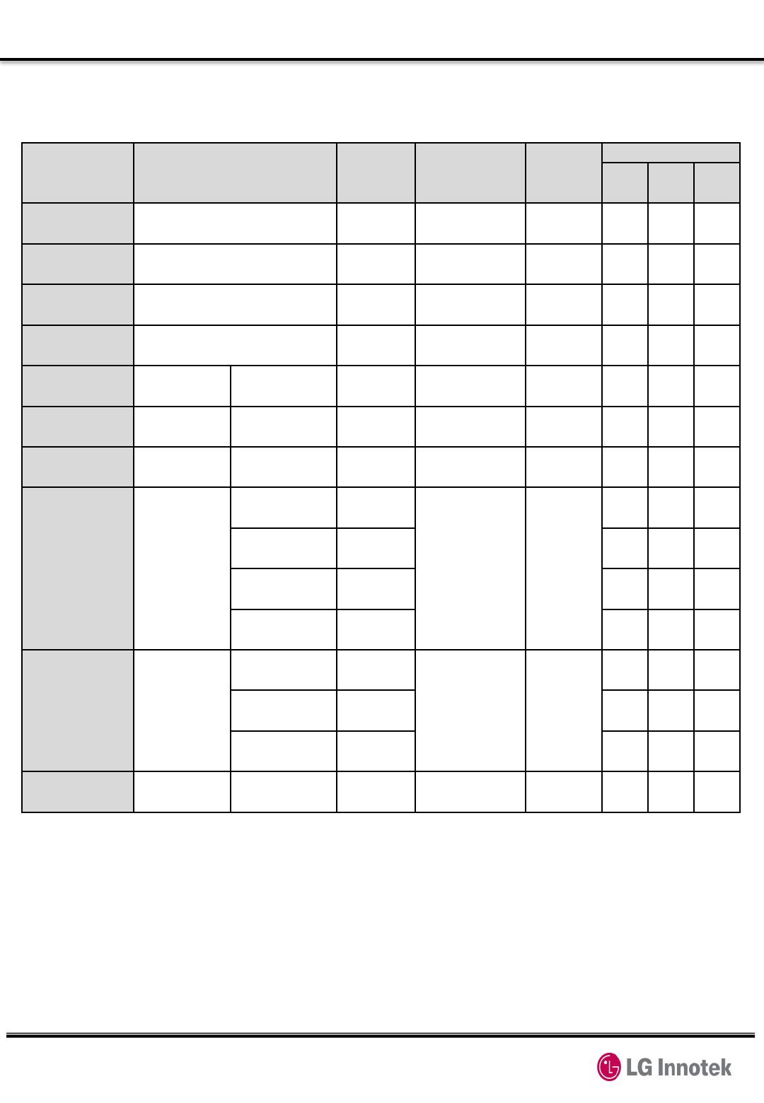
7.3 LTE B2 electrical specifications
시험 항목 Spec. Test Temperature Frequency
TX Channel
18650 18900 19150
1 Maximum Output Power(class 3) 20.3~25.7dBm Normal, Temp L, Temp H Low, Mid, High PASS PASS PASS
2 Minimum Output Power -39dBm ↓ Normal, Temp L, Temp H Low, Mid, High PASS PASS PASS
3 Frequency Error ±0.1ppm Normal, Temp L, Temp H Low, Mid, High PASS PASS PASS
4 Error Vector Magnitude(EVM)
12.5%↓(16QAM,
50RB) Normal Low, Mid, High PASS PASS PASS
5 Relative Carrier
Leakage Power
Carrier Leakage
(3.2dBm ± 3.2dB) -24.2 dBc Normal, Temp L, Temp H Low, Mid, High PASS PASS PASS
6 In-band emission In-band emission
(3.2dBm ± 3.2dB) -24.2 dBc Normal, Temp L, Temp H Low, Mid, High PASS PASS PASS
7 EVM equalizer
spectrum flatness
EVM equalizer spectrum
flatness Range1 5.4 dB ↓ Normal, Temp L, Temp H Low, Mid, High PASS PASS PASS
8 Spectrum emission
mask
Spectrum Emission Mask
upper/lower Area 1 -16.5 dBm ↓
Normal Low, Mid, High
PASS PASS PASS
Spectrum Emission Mask
upper/lower Area 2 -8.5 dBm ↓ PASS PASS PASS
Spectrum Emission Mask
upper/lower Area 3 -11.5 dBm ↓ PASS PASS PASS
Spectrum Emission Mask
upper/lower Area 4 -23.5 dBm ↓ PASS PASS PASS
9 Adjacent Channel
Leakage Power Ratio
ACLR E-UTRA ± -29.2dB ↓
Normal, Temp L, Temp H Low, Mid, High
PASS PASS PASS
ACLR UTRA Offset 1 ± -32.2dB ↓ PASS PASS PASS
ACLR UTRA Offset 2 ± -35.2dB ↓ PASS PASS PASS
10
Reference Sensitivity
Level @ 10MHz
Ref Sense throughput
shall be ≥ 95% -94.3 dBm Normal, Temp L, Temp H Low, Mid, High PASS PASS PASS
Table 10. LTE B2 RF specification

Copyright ⓒ. 2017. All Rights Reserved.
7. General specifications
7.4 LTE B4 electrical specifications
시험 항목 Spec. Test Temperature Frequency
TX Channel
20000 20175 20350
1 Maximum Output Power(class 3) 20.3~25.7dBm Normal, Temp L, Temp H Low, Mid, High PASS PASS PASS
2 Minimum Output Power -39dBm ↓ Normal, Temp L, Temp H Low, Mid, High PASS PASS PASS
3 Frequency Error ±0.1ppm Normal, Temp L, Temp H Low, Mid, High PASS PASS PASS
4 Error Vector Magnitude(EVM)
12.5%↓(16QAM,
50RB) Normal Low, Mid, High PASS PASS PASS
5 Relative Carrier
Leakage Power
Carrier Leakage
(3.2dBm ± 3.2dB) -24.2 dBc Normal, Temp L, Temp H Low, Mid, High PASS PASS PASS
6 In-band emission In-band emission
(3.2dBm ± 3.2dB) -24.2 dBc Normal, Temp L, Temp H Low, Mid, High PASS PASS PASS
7 EVM equalizer
spectrum flatness
EVM equalizer spectrum
flatness Range1 5.4 dB ↓ Normal, Temp L, Temp H Low, Mid, High PASS PASS PASS
8 Spectrum emission
mask
Spectrum Emission Mask
upper/lower Area 1 -16.5 dBm ↓
Normal Low, Mid, High
PASS PASS PASS
Spectrum Emission Mask
upper/lower Area 2 -8.5 dBm ↓ PASS PASS PASS
Spectrum Emission Mask
upper/lower Area 3 -11.5 dBm ↓ PASS PASS PASS
Spectrum Emission Mask
upper/lower Area 4 -23.5 dBm ↓ PASS PASS PASS
9 Adjacent Channel
Leakage Power Ratio
ACLR E-UTRA ± -29.2dB ↓
Normal, Temp L, Temp H Low, Mid, High
PASS PASS PASS
ACLR UTRA Offset 1 ± -32.2dB ↓ PASS PASS PASS
ACLR UTRA Offset 2 ± -35.2dB ↓ PASS PASS PASS
10
Reference Sensitivity
Level @ 10MHz
Ref Sense throughput
shall be ≥ 95% -96.3 dBm Normal, Temp L, Temp H Low, Mid, High PASS PASS PASS
Table 11. LTE B4 RF specification

Copyright ⓒ. 2017. All Rights Reserved.
7. General specifications
7.5 LTE B5 electrical specifications
시험 항목 Spec. Test Temperature Frequency
TX Channel
20450 20525 20600
1 Maximum Output Power(class 3) 20.3~25.7dBm Normal, Temp L, Temp H Low, Mid, High PASS PASS PASS
2 Minimum Output Power -39dBm ↓ Normal, Temp L, Temp H Low, Mid, High PASS PASS PASS
3 Frequency Error ±0.1ppm Normal, Temp L, Temp H Low, Mid, High PASS PASS PASS
4 Error Vector Magnitude(EVM)
12.5%↓(16QAM,
50RB) Normal Low, Mid, High PASS PASS PASS
5 Relative Carrier
Leakage Power
Carrier Leakage
(3.2dBm ± 3.2dB) -24.2 dBc Normal, Temp L, Temp H Low, Mid, High PASS PASS PASS
6 In-band emission In-band emission
(3.2dBm ± 3.2dB) -24.2 dBc Normal, Temp L, Temp H Low, Mid, High PASS PASS PASS
7 EVM equalizer
spectrum flatness
EVM equalizer spectrum
flatness Range1 5.4 dB ↓ Normal, Temp L, Temp H Low, Mid, High PASS PASS PASS
8 Spectrum emission
mask
Spectrum Emission Mask
upper/lower Area 1 -16.5 dBm ↓
Normal Low, Mid, High
PASS PASS PASS
Spectrum Emission Mask
upper/lower Area 2 -8.5 dBm ↓ PASS PASS PASS
Spectrum Emission Mask
upper/lower Area 3 -11.5 dBm ↓ PASS PASS PASS
Spectrum Emission Mask
upper/lower Area 4 -23.5 dBm ↓ PASS PASS PASS
9 Adjacent Channel
Leakage Power Ratio
ACLR E-UTRA ± -29.2dB ↓
Normal, Temp L, Temp H Low, Mid, High
PASS PASS PASS
ACLR UTRA Offset 1 ± -32.2dB ↓ PASS PASS PASS
ACLR UTRA Offset 2 ± -35.2dB ↓ PASS PASS PASS
10
Reference Sensitivity
Level @ 10MHz
Ref Sense throughput
shall be ≥ 95% -94.3 dBm Normal, Temp L, Temp H Low, Mid, High PASS PASS PASS
Table 12. LTE B5 RF specification
Copyright ⓒ. 2017. All Rights Reserved.
7. General specifications
7.17 LTE B17 electrical specifications
Table 13. LTE B17 RF specification
시험 항목 Spec. Test Temperature Frequency
TX Channel
23780 23790 23800
1 Maximum Output Power(class 3) 20.3~25.7dBm Normal, Temp L, Temp H Low, Mid, High PASS PASS PASS
2 Minimum Output Power -39dBm ↓ Normal, Temp L, Temp H Low, Mid, High PASS PASS PASS
3 Frequency Error ±0.1ppm Normal, Temp L, Temp H Low, Mid, High PASS PASS PASS
4 Error Vector Magnitude(EVM)
12.5%↓(16QAM,
50RB) Normal Low, Mid, High PASS PASS PASS
5 Relative Carrier
Leakage Power
Carrier Leakage
(3.2dBm ± 3.2dB) -24.2 dBc Normal, Temp L, Temp H Low, Mid, High PASS PASS PASS
6 In-band emission In-band emission
(3.2dBm ± 3.2dB) -24.2 dBc Normal, Temp L, Temp H Low, Mid, High PASS PASS PASS
7 EVM equalizer
spectrum flatness
EVM equalizer spectrum
flatness Range1 5.4 dB ↓ Normal, Temp L, Temp H Low, Mid, High PASS PASS PASS
8 Spectrum emission
mask
Spectrum Emission Mask
upper/lower Area 1 -16.5 dBm ↓
Normal Low, Mid, High
PASS PASS PASS
Spectrum Emission Mask
upper/lower Area 2 -8.5 dBm ↓ PASS PASS PASS
Spectrum Emission Mask
upper/lower Area 3 -11.5 dBm ↓ PASS PASS PASS
Spectrum Emission Mask
upper/lower Area 4 -23.5 dBm ↓ PASS PASS PASS
9 Adjacent Channel
Leakage Power Ratio
ACLR E-UTRA ± -29.2dB ↓
Normal, Temp L, Temp H Low, Mid, High
PASS PASS PASS
ACLR UTRA Offset 1 ± -32.2dB ↓ PASS PASS PASS
ACLR UTRA Offset 2 ± -35.2dB ↓ PASS PASS PASS
10
Reference Sensitivity
Level @ 10MHz
Ref Sense throughput
shall be ≥ 95% -93.3 dBm Normal, Temp L, Temp H Low, Mid, High PASS PASS PASS

Copyright ⓒ. 2017. All Rights Reserved.
8. RFx information
The strength of the RF field produced by the wireless module or modules
embedded in the TCU is well within all international RF exposure limits known
at this time. Because the wireless modules embedded in the TCU emit less than
the maximum amount of energy permitted in radio frequency safety standards
and recommendations, the manufacturer believes these modules are safe for
use.
Regardless of the power levels, care should be taken to minimize human
contact during normal operation. This module should be remain more than 20
cm (8 inches) from the body when wireless devices are on and transmitting.
This transmitter must not be collocated or operated in conjunction with any
other antenna or transmitter. Operation is subject to the following two conditions:
(1) this module does not cause interference , (2) this module accepts any
interference that may cause undesired operation.
8.1 Information for the integrator
The integrator must not provide information to the end user regarding how to
install or remove this RF module in the user manual of the end product. The user
manual that is provided by the integrator for end users must include the following
information in a prominent location. To comply with FCC RF exposure
requirements, the antenna used for this transmitter must be installed to provide a
separation distance of at least 20 cm from all persons and must not be
collocated or operated in conjunction with any other antenna or transmitter. The
label for the end product must include FCC ID: YZP-BK1000 or A RF transmitter
inside, IC ID: 7414C-BK1000
Copyright ⓒ. 2017. All Rights Reserved.
9. Approbation FCC
This module complies with FCC/IC rules.
FCC : Part 22, Part 24, Part 27
IC : RSS-130, RSS-132, RSS-133, RSS-139
Furthermore, this device complies with FCC/IC radiation exposure limits set forth for uncontrolled
environments.
This module must be installed and operated with minimum distance of 20 cm between the radiating element
and the user.
This module must not be co-located with any other transmitters or antennas
Cet module est conforme à l'exposition de FCC et IC rayonnements limites é-tablies pour un environnement
non contrôlé. Cet module doit être installé et utilisé avec une distance minimale de 20 cm entre le radiateur et
votre corps. Ce module ne doit pas être même endroit avec d'autres émetteur ou antennes.
To comply with FCC/IC regulations limiting both the maximum RF output power and human exposure to RF
radiation, the maximum antenna gain including cable loss in a mobile-only exposure condition must not
exceed the values listed in the following table.
To satisfy the FCC’s exterior labeling requirements, the following text must appear on the
exterior of the end product.
Contains transmitter module FCC ID: YZP-BK1000
Contains transmitter module IC ID: 7414C-BK1000
Changes or modifications to this equipment may cause harmful interference unless the
modifications are expressly approved in the instruction manual. Users may lose the authority
to operate this equipment if an unauthorized change or codification is made.
Note: If this module is intended for use in a portable device, additional testing will be required
to satisfy the RF exposure and SAR requirements of FCC Part 2.1093 and RSS-102.
Band Frequency Range
[MHz] Maximum Antenna
Gain[dBi]
WCDMA(B5) 826.40~846.6 4.5
WCDMA(B2) 1852.4~1907.6 2.0
LTE(B2) 1850~1910 2.0
LTE(B4) 1710~1755 2.0
LTE(B5) 824~849 4.5
LTE(B17) 704~716 4.5