LG Innotek TWZTV001D Wireless Module for Lighting Control User Manual
LG Innotek Co., Ltd. Wireless Module for Lighting Control
UserManual.wiki
>
LG Innotek
>
TWZTV001D User Manual
User Manual
Navigation menu
Upload a User Manual
Namespaces
Wiki Guide
HTML
PDF
Info
Views
User Manual
Discussion / Help
Navigation
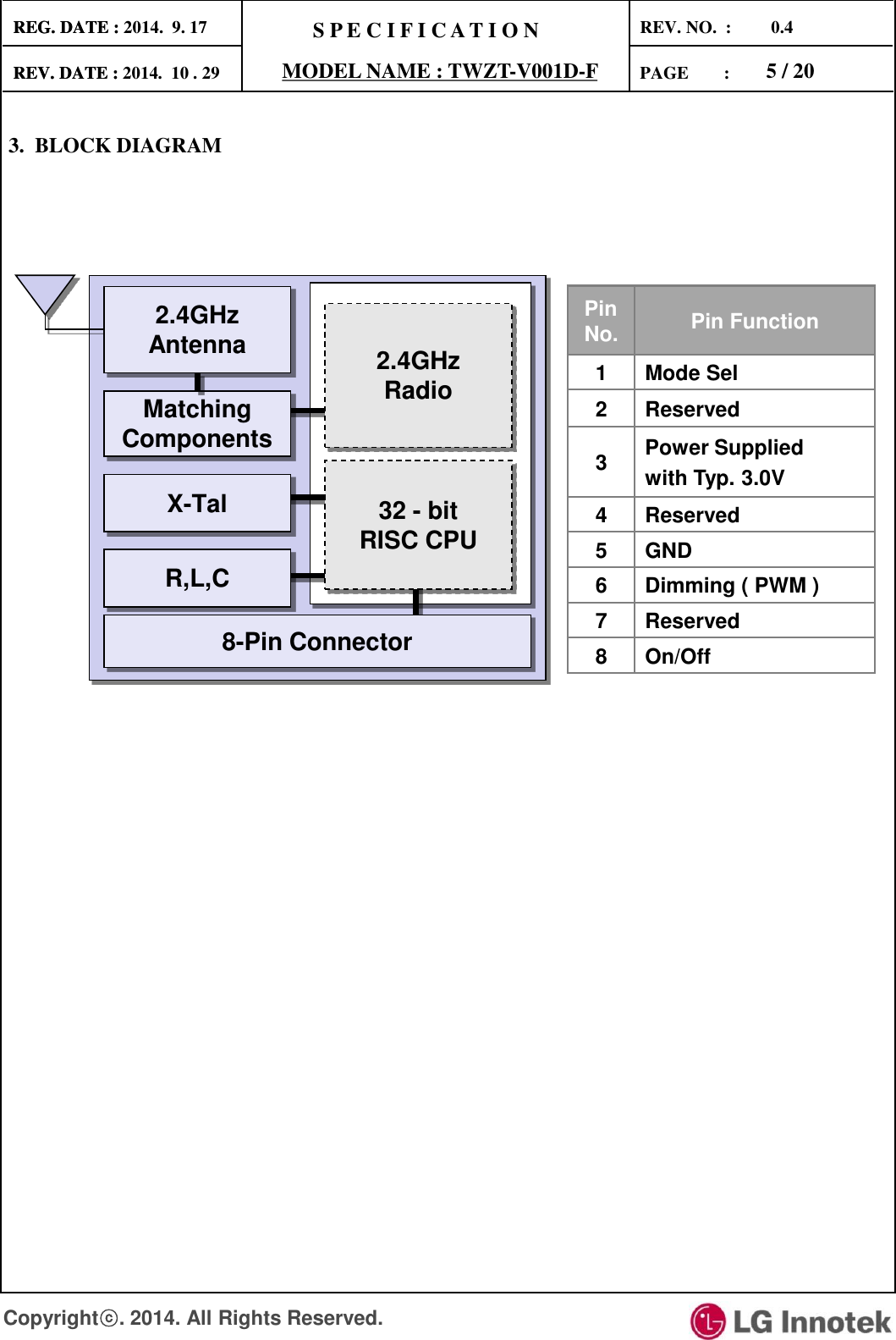
![S P E C I F I C A T I O N PAGE : REG. DATE : MODEL NAME : TWZT-V001D-F REV. DATE : . . REV. NO. : 0.4 REG. DATE : 2014. 9. 17 REV. DATE : 2014 10 29 6 / 20 Copyrightⓒ. 2014. All Rights Reserved. 4. ABSOLUTE MAXIMUM RATING⑴ NO ITEM RATING UNIT 1 Supply voltage All supply pins must have the same voltage⑴ 3.6 V 2 Storage temperature range -20 ~ 85 ℃ 3 Input RF level 10 dBm 6. GENERAL CHARACTERISTICS Measured on LG Innotek [TWZT-V001D-F] design with VDD = 3.0V and TA=25℃, Unless otherwise noted. all limits apply over the entire operating range, TA = -20 ~ +85℃, VDD 3.0±0.3 and fc = 2.4 ~ 2.5GHz NO ITEM RATING UNIT 1 Operating ambient Temperature Range, TA -20 ~ +85 ℃ 2 Operating supply voltage (Typ. 3.0v), Power Ripple ±100mV 2.7 ~ 3.3 V 5. RECOMMENDED OPERATING CONDITIONS (1) Stresses beyond those listed under Absolute Maximum Ratings may cause permanent damage to the device. These are stress ratings only, and functional operation of the device at these or any other conditions beyond those indicated under Recommended Operating Conditions is not implied. Exposure to absolute-maximum-rated conditions for extended periods may affect device reliability. NO Test Item MIN. Typ. MAX. Unit Condition 1 Operating Supply Voltage 2.7 3.0 3.3 V - 2 Frequency Range 2400 - 2483.5 MHz 5MHz Channel Spacing 3 Peak Current Consumption Tx( at +6 dBm) 40 45 50 mA Active-Mode Rx( Boost mode ) 23 28 33 mA Active-Mode 4 ESD -15 - +15 KV Air Condition, No Electrical Problem -2.0 - +2.0 KV Contact Condition, No Electrical Problem](https://usermanual.wiki/LG-Innotek/TWZTV001D/User-Guide-2448198-Page-6.png)
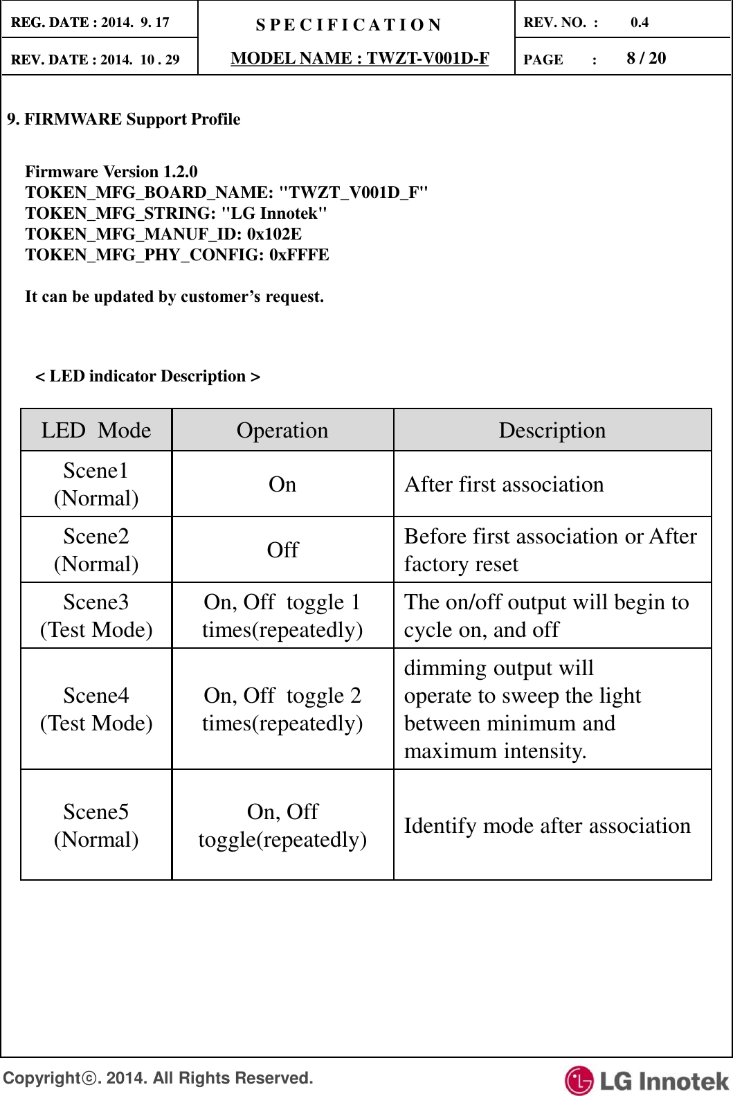
![S P E C I F I C A T I O N PAGE : REG. DATE : MODEL NAME : TWZT-V001D-F REV. DATE : . . REV. NO. : 0.4 REG. DATE : 2014. 9. 17 REV. DATE : 2014 10 29 7 / 20 Copyrightⓒ. 2014. All Rights Reserved. NO Test Item MIN. Typ. MAX. Unit Condition 1 Nominal Output Power 3 6 - dBm Single Ended 50Ω Load (Required Min.-3dBm) 2 Receiver Sensitivity - -100 -94 dBm PER=1% (Required -85dBm) 3 Maximum Input Level - - 0 dBm PER=1% (Required -20dBm) 4 Frequency Tolerance -20 - +20 ppm All Operating Temp. (Required Max. ±40ppm) 5 Error Vector Magnitude (EVM) - 10 35 % ( Required Max. 35% ) 6 Harmonic - - -31 dBm 2nd Harmonic - -31 dBm 3rd Harmonic 7 Spurious Emissions - - -31 dBm All Band (30MHZ ~ 12.5GHz) Measured on LG Innotek [TWZT-V001D-F] design with VDD = 3.0V and Ta=25℃, RF Conducted Test, Unless otherwise noted. All limits apply over the entire operating range, Ta =-20 ~ +85℃ , VDD 3.0±0.3 and fc = 2.4 ~ 2.4835 GHz 7. RF SPECIFICATION ( Required ~ ) : refer to IEEE 802.15.4 8. ANTENNA SPECIFICATION NO Test Item MIN. Typ. MAX. Unit Condition 1 Frequency Range 2.4 - 2.4835 GHz All Operating Temp. 2 Nominal Impedance - 50 - Ω 3 Band width - 80 - MHz All Band (30MHZ ~ 12.5GHz) 4 Internal Antenna Passive efficiency 45 50 - % Single Antenna unit(Only) 5 Internal Antenna VSWR - 1.5:1 2.5:1 - Single Antenna unit(Only) 6 Peak Gain 3.0 dB Single Antenna unit(Only) 7 Directivity 6.0 dB Single Antenna unit(Only) Condition : It can be changed by measurement condition(only R&D Environment) Mechanical Information : Size : 15×5.5×0.9mm, PCB Material Fr-4 (4.4 εr)](https://usermanual.wiki/LG-Innotek/TWZTV001D/User-Guide-2448198-Page-7.png)
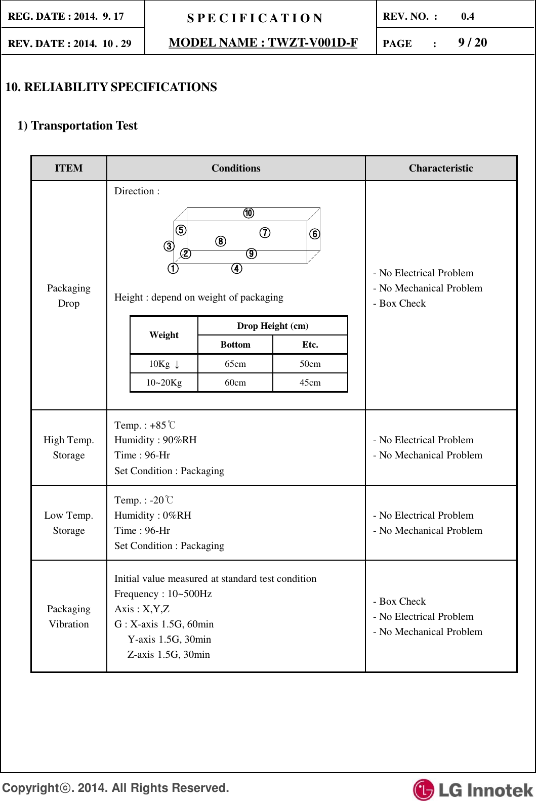
![S P E C I F I C A T I O N PAGE : REG. DATE : MODEL NAME : TWZT-V001D-F REV. DATE : . . REV. NO. : 0.4 REG. DATE : 2014. 9. 17 REV. DATE : 2014 10 29 11 / 20 Copyrightⓒ. 2014. All Rights Reserved. *It can be changed (Not fixed) ITEM Conditions Characteristic Temperature & Humidity Cycle Initial value measured at standard test condition Temp./Humidity : : [25℃→55℃(3h),55℃(9h), 55℃→25℃(3h),25℃(9h)] X6 / 95%, 144Hrs. Measuring After 1-2hr at standard conditions - No Electrical Problem Thermal Shock Test -20℃~85℃ 100Cycle Measuring After 1-2hr at standard conditions. - No Electrical Problem Vibration Test Initial value measured at standard test condition Frequency : 10~500Hz Axis : X,Y,Z G : X-axis 1.5G, 60min Y-axis 1.5G, 30min Z-axis 1.5G, 30min - No Electrical Problem ESD Test Condition - Contact : 150PF / 330Ω, ± 2 kV, 10 times - Air : 150PF / 330Ω, ± 15kV, 10 times All functions and playing shall be recovered after ESD hit without reboot for reset.](https://usermanual.wiki/LG-Innotek/TWZTV001D/User-Guide-2448198-Page-11.png)
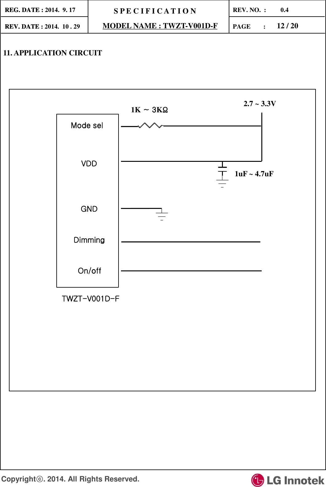
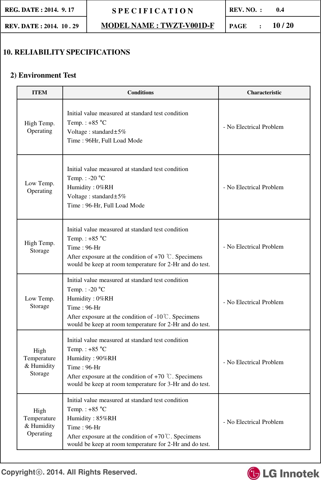
![S P E C I F I C A T I O N PAGE : REG. DATE : MODEL NAME : TWZT-V001D-F REV. DATE : . . REV. NO. : 0.4 REG. DATE : 2014. 9. 17 REV. DATE : 2014 10 29 13 / 20 Copyrightⓒ. 2014. All Rights Reserved. 12. MODULE INTERFACE [ PIN DESCRIPTION ] < Host Interface with PSU > -. PWM Mode No. I/O Pin Name Descrption 1 I Mode Sel Low -> Test mode 2 - GPIO1 Reserved 3 - VDD Power Supply Typ. 3.0V (2.7V ~ 3.3V) 4 O GPIO2 Reserved 5 - GND Ground 6 O Dim Dimming Control 7 O GPIO3 Reserved 8 O On/off On/off Control * Recommended Dimming & On/off Pin Initial State : Pull up ① ② ③ ④ ⑤ ⑥ ⑦ ⑧](https://usermanual.wiki/LG-Innotek/TWZTV001D/User-Guide-2448198-Page-13.png)