LG Innotek TWZTV001D Wireless Module for Lighting Control User Manual
LG Innotek Co., Ltd. Wireless Module for Lighting Control
User Manual
SPECIFICATIONS
PRODUCT NAME : Wireless Module for Lighting Control
MODEL NAME : TWZT-V001D-F
CUSTOMER MODEL NAME :
Designed Checked Approved
LG Innotek Co., Ltd.
Ro
Young
Suk
Kim
Yong
Gyu DOCUMENT No. 14-RFM-0174
‘14.09.17 ‘14.09.17 ‘14.09.17 PAGE 21
The information contained herein is the exclusive property of LG Innotek
and shall not be distributed, reproduced or disclosed in whole or no in part
without prior written permission of LG Innotek.
Yun
Yeong
Uk
S P E C I F I C A T I O N
PAGE :
REG. DATE :
MODEL NAME : TWZT-V001D-F
REV. DATE : . .
REV. NO. : 0.4 REG. DATE : 2014. 9. 17
REV. DATE : 2014 10 29 2 / 20
Copyrightⓒ. 2014. All Rights Reserved.
Record of Revision
Revision Date Revision Description Remark
0.1 2014.09.17 Initial Release.
0.2 2014.10.07 Temperture spec changed.
0.3 2014.10.22 Current spec changed.
Firmware Version Updated.
0.4 2014.10.29 Label spec Updated.

S P E C I F I C A T I O N
PAGE :
REG. DATE :
MODEL NAME : TWZT-V001D-F
REV. DATE : . .
REV. NO. : 0.4 REG. DATE : 2014. 9. 17
REV. DATE : 2014 10 29 3 / 20
Copyrightⓒ. 2014. All Rights Reserved.
CONTENTS
1. GENERAL DESCRIPTION
2. FEATURES
3. BLOCK DIAGRAM
4. ABSOLUTE MAXIMUM RATING
5. RECOMMENDED OPERATING CONDITION
6. GENERAL CHARACTERISTICS
7. RF SPECIFICATIONS
8. ANTENNA SPECIFICATIONS
9. FIRMWARE INFORMTION
10. RELIABILITY SPECIFICATIONS
11. APPLICATION CIRCUIT
12. MODULE INTERFACE
13. MECHANICAL INFORMATION
14. PRODUCT LABEL INFORMATION
15. PACKING INFORMATION
16. ORDERING INFORMATION
S P E C I F I C A T I O N
PAGE :
REG. DATE :
MODEL NAME : TWZT-V001D-F
REV. DATE : . .
REV. NO. : 0.4 REG. DATE : 2014. 9. 17
REV. DATE : 2014 10 29 4 / 20
Copyrightⓒ. 2014. All Rights Reserved.
1. GENERAL DESCRIPTION
LG Innotek’s Common Zigbee Module solution for IEEE 802.15.4, Zigbee( ZHA ) and RF4CE
applications. In addition, this modules are high performance hardware feature and easy connectivity
solution for wireless lighting control and smart home applications. It enables robust network nodes to
be built with very low total bill-of material costs. This module is suited for systems where very low
power consumption is required. Very low-power sleep modes are available. Short transition times
between operating modes further enable low power consumption.
LG Innotek‘s common Zigbee Module contains the RF IC and necessary external components and
integrated very small size PCB pattern Antenna. It is provides very simple hardware support for easy
smart lighting control and WSN applications
2. FEATURES
- 2.4GHz IEEE802.15.4 compliant RF Transceiver
- Excellent Receiver Sensitivity and Robustness to
interference
- Programmable Output Power Up to 6.5 dBm
- Small Module with PCB Pattern Antenna Solution
: Size 22×29×7.7mm
- High performance and Low power 32-bit
RISC CPU
- 192-KB In-System-Programmable Flash and
External 256-KB Flash for OTA(Over the Air)
- 8-Pin connection for Power Supply Unit
- Support Standard Protocol ( ZHA )
- Support Wireless S/W Upgrade( OTA : Over the Air )
S P E C I F I C A T I O N
PAGE :
REG. DATE :
MODEL NAME : TWZT-V001D-F
REV. DATE : . .
REV. NO. : 0.4 REG. DATE : 2014. 9. 17
REV. DATE : 2014 10 29 5 / 20
Copyrightⓒ. 2014. All Rights Reserved.
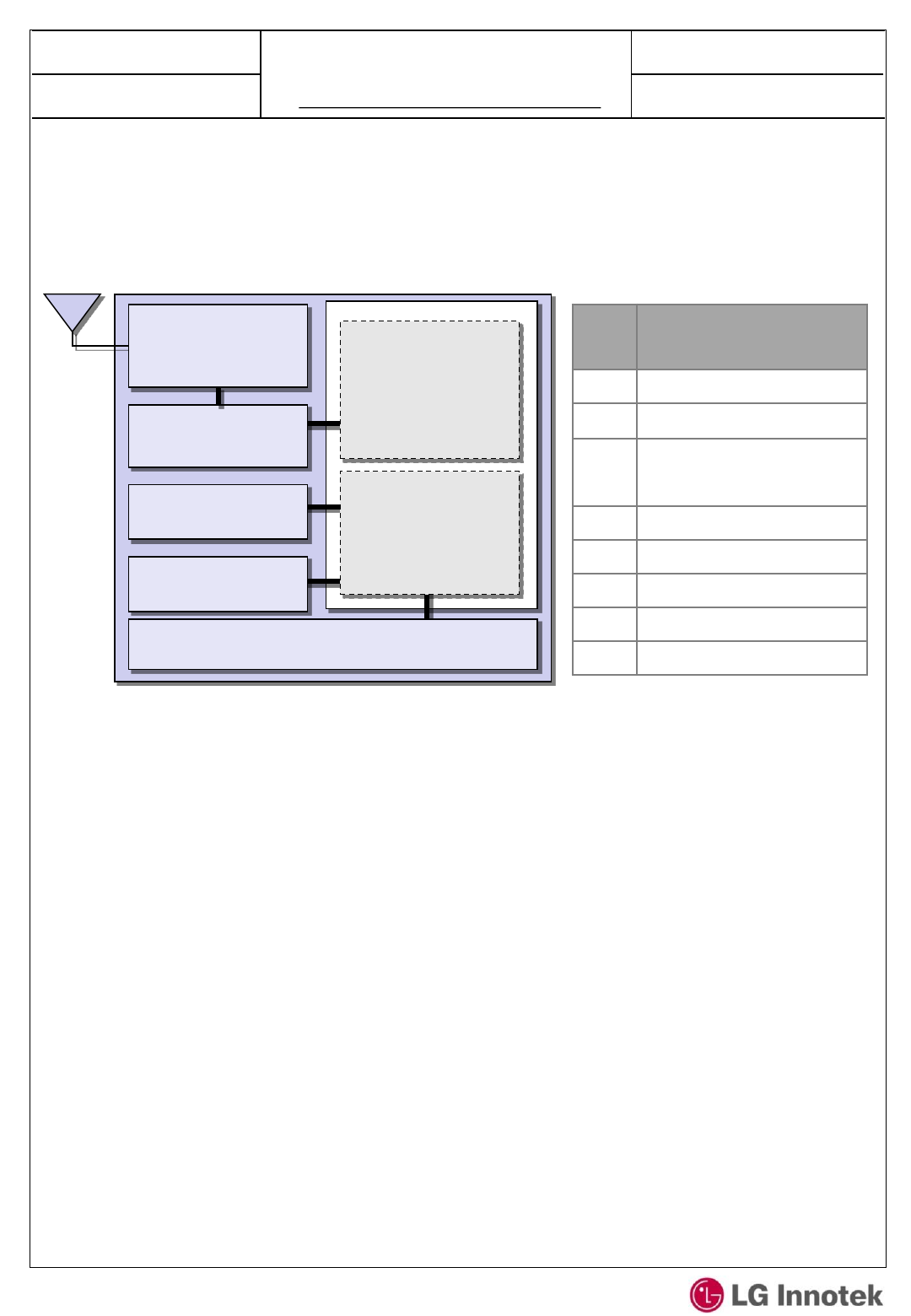
3. BLOCK DIAGRAM
2.4GHz
Radio
32 - bit
RISC CPU
2.4GHz
Antenna
Matching
Components
X-Tal
R,L,C
8-Pin Connector
Pin
No. Pin Function
1 Mode Sel
2 Reserved
3 Power Supplied
with Typ. 3.0V
4 Reserved
5 GND
6 Dimming ( PWM )
7 Reserved
8 On/Off
S P E C I F I C A T I O N
PAGE :
REG. DATE :
MODEL NAME : TWZT-V001D-F
REV. DATE : . .
REV. NO. : 0.4 REG. DATE : 2014. 9. 17
REV. DATE : 2014 10 29 6 / 20
Copyrightⓒ. 2014. All Rights Reserved.
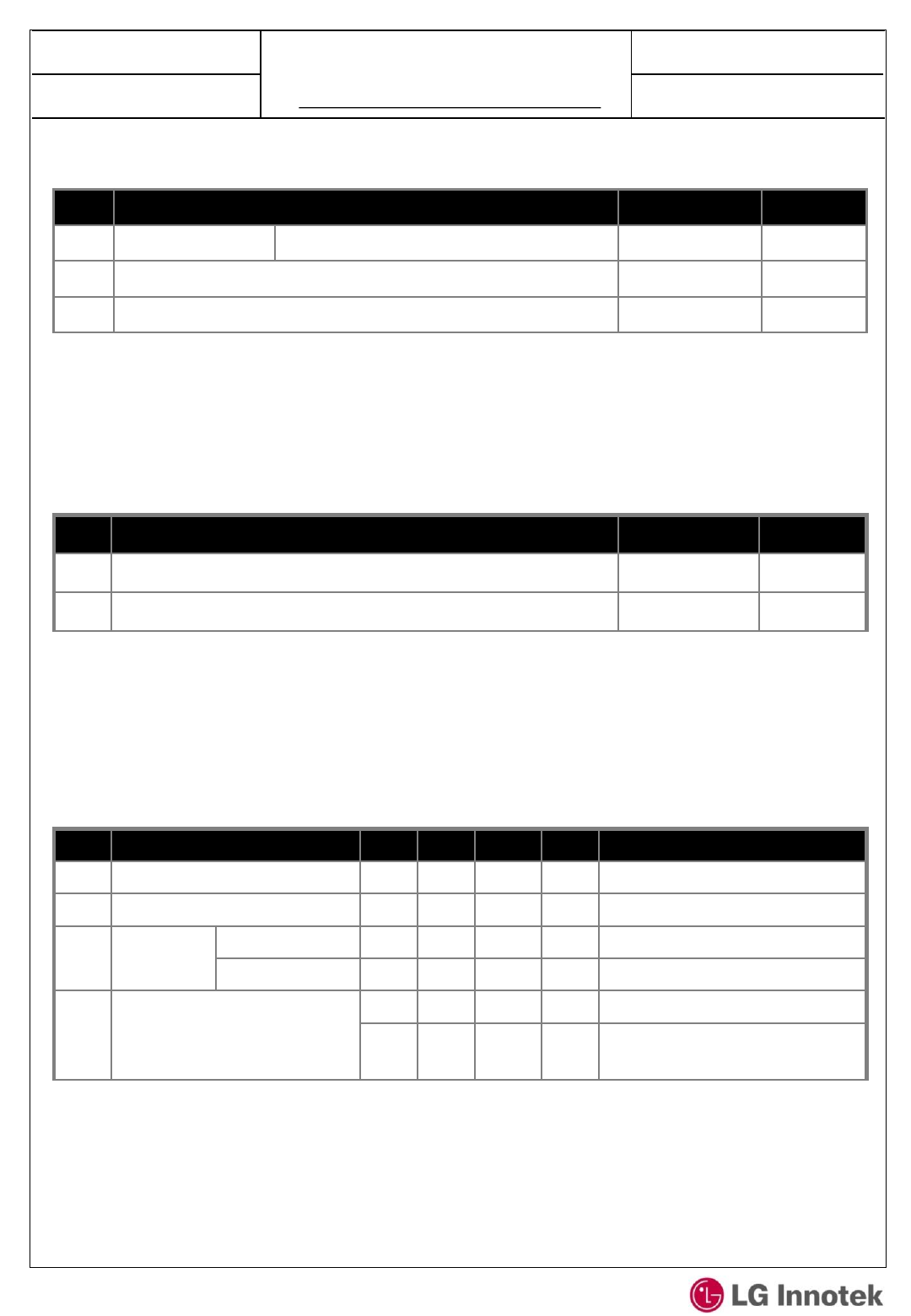
4. ABSOLUTE MAXIMUM RATING⑴
NO ITEM RATING UNIT
1 Supply voltage All supply pins must have the same voltage⑴ 3.6 V
2 Storage temperature range -20 ~ 85 ℃
3 Input RF level 10 dBm
6. GENERAL CHARACTERISTICS
Measured on LG Innotek [TWZT-V001D-F] design with VDD = 3.0V and TA=25℃, Unless otherwise noted. all
limits apply over the entire operating range, TA = -20 ~ +85℃, VDD 3.0±0.3 and fc = 2.4 ~ 2.5GHz
NO ITEM RATING UNIT
1 Operating ambient Temperature Range, TA -20 ~ +85 ℃
2 Operating supply voltage (Typ. 3.0v), Power Ripple ±100mV 2.7 ~ 3.3 V
5. RECOMMENDED OPERATING CONDITIONS
(1) Stresses beyond those listed under Absolute Maximum Ratings may cause permanent damage to the device. These are stress
ratings only, and functional operation of the device at these or any other conditions beyond those indicated under Recommended
Operating Conditions is not implied. Exposure to absolute-maximum-rated conditions for extended periods may affect device
reliability.
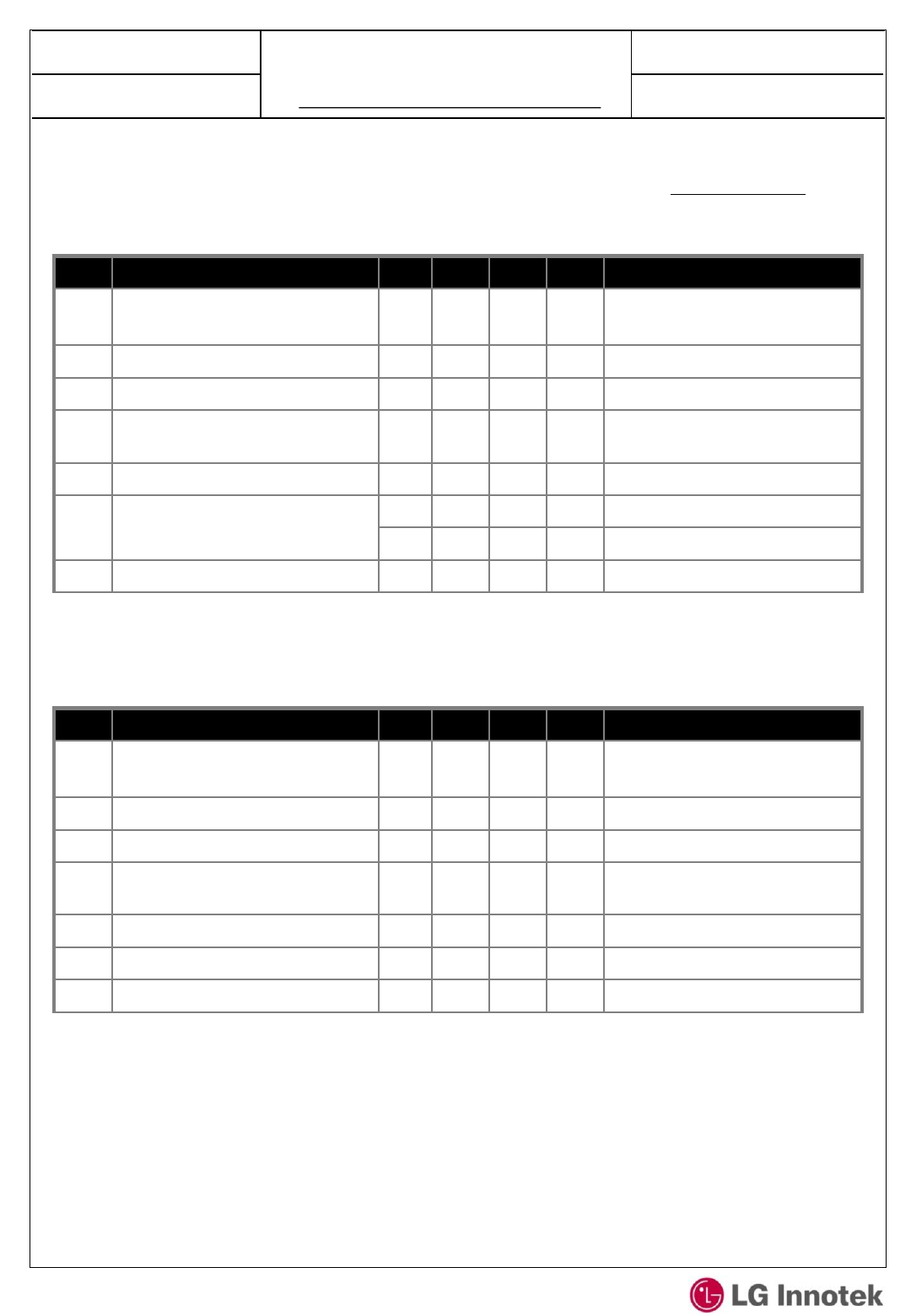
NO Test Item MIN. Typ. MAX. Unit Condition
1 Operating Supply Voltage 2.7 3.0 3.3 V -
2 Frequency Range 2400 - 2483.5 MHz 5MHz Channel Spacing
3 Peak Current
Consumption
Tx( at +6 dBm) 40 45 50 mA Active-Mode
Rx( Boost mode ) 23 28 33 mA Active-Mode
4 ESD
-15 - +15 KV Air Condition, No Electrical Problem
-2.0 - +2.0 KV Contact Condition,
No Electrical Problem
S P E C I F I C A T I O N
PAGE :
REG. DATE :
MODEL NAME : TWZT-V001D-F
REV. DATE : . .
REV. NO. : 0.4 REG. DATE : 2014. 9. 17
REV. DATE : 2014 10 29 7 / 20
Copyrightⓒ. 2014. All Rights Reserved.
NO Test Item MIN. Typ. MAX. Unit Condition
1 Nominal Output Power 3 6 - dBm Single Ended 50Ω Load
(Required Min.-3dBm)
2 Receiver Sensitivity - -100 -94 dBm PER=1% (Required -85dBm)
3 Maximum Input Level - - 0 dBm PER=1% (Required -20dBm)
4 Frequency Tolerance -20 - +20 ppm All Operating Temp. (Required
Max. ±40ppm)
5 Error Vector Magnitude (EVM) - 10 35 % ( Required Max. 35% )
6 Harmonic - - -31 dBm 2nd Harmonic
- -31 dBm 3rd Harmonic
7 Spurious Emissions - - -31 dBm All Band (30MHZ ~ 12.5GHz)
Measured on LG Innotek [TWZT-V001D-F] design with VDD = 3.0V and Ta=25℃, RF Conducted Test, Unless
otherwise noted. All limits apply over the entire operating range, Ta =-20 ~ +85℃ , VDD 3.0±0.3 and fc = 2.4 ~
2.4835 GHz
7. RF SPECIFICATION
( Required ~ ) : refer to IEEE 802.15.4
8. ANTENNA SPECIFICATION
NO Test Item MIN. Typ. MAX. Unit Condition
1 Frequency Range 2.4 - 2.4835 GHz All Operating Temp.
2 Nominal Impedance - 50 - Ω
3 Band width - 80 - MHz All Band (30MHZ ~ 12.5GHz)
4 Internal Antenna Passive efficiency 45 50 - % Single Antenna unit(Only)
5 Internal Antenna VSWR - 1.5:1 2.5:1 - Single Antenna unit(Only)
6 Peak Gain 3.0 dB Single Antenna unit(Only)
7 Directivity 6.0 dB Single Antenna unit(Only)
Condition : It can be changed by measurement condition(only R&D Environment)
Mechanical Information : Size : 15×5.5×0.9mm, PCB Material Fr-4 (4.4 εr)
S P E C I F I C A T I O N
PAGE :
REG. DATE :
MODEL NAME : TWZT-V001D-F
REV. DATE : . .
REV. NO. : 0.4 REG. DATE : 2014. 9. 17
REV. DATE : 2014 10 29 8 / 20
Copyrightⓒ. 2014. All Rights Reserved.
Firmware Version 1.2.0
TOKEN_MFG_BOARD_NAME: "TWZT_V001D_F"
TOKEN_MFG_STRING: "LG Innotek"
TOKEN_MFG_MANUF_ID: 0x102E
TOKEN_MFG_PHY_CONFIG: 0xFFFE
It can be updated by customer’s request.
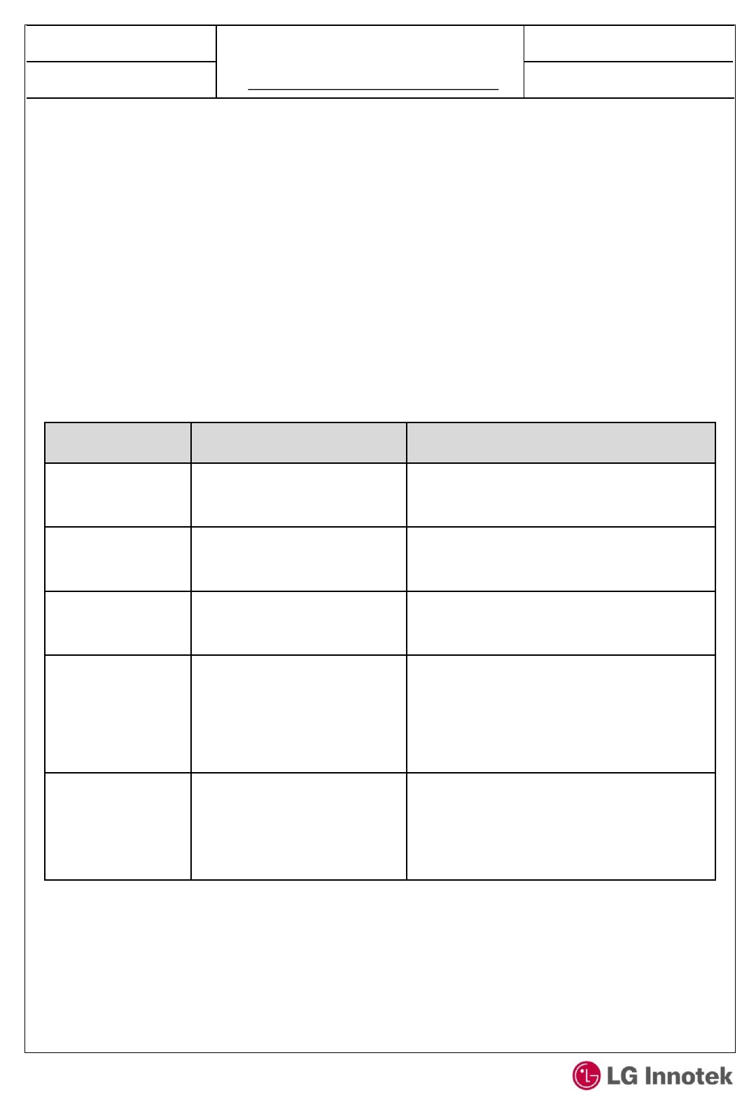
9. FIRMWARE Support Profile
LED Mode Operation Description
Scene1
(Normal) On
After first association
Scene2
(Normal) Off
Before first association
or After
factory reset
Scene3
(Test Mode)
On, Off toggle 1
times(repeatedly)
The on/off output will begin to
cycle on, and off
Scene4
(Test Mode)
On, Off toggle 2
times(repeatedly)
dimming output will
operate to sweep the light
between minimum and
maximum intensity.
Scene5
(Normal) On, Off
toggle(repeatedly)
Identify mode after
association
< LED indicator Description >
S P E C I F I C A T I O N
PAGE :
REG. DATE :
MODEL NAME : TWZT-V001D-F
REV. DATE : . .
REV. NO. : 0.4 REG. DATE : 2014. 9. 17
REV. DATE : 2014 10 29 9 / 20
Copyrightⓒ. 2014. All Rights Reserved.
10. RELIABILITY SPECIFICATIONS
1) Transportation Test
ITEM Conditions Characteristic
Packaging
Drop
Direction :
Height : depend on weight of packaging
- No Electrical Problem
- No Mechanical Problem
- Box Check
High Temp.
Storage
Temp. : +85℃
Humidity : 90%RH
Time : 96-Hr
Set Condition : Packaging
- No Electrical Problem
- No Mechanical Problem
Low Temp.
Storage
Temp. : -20℃
Humidity : 0%RH
Time : 96-Hr
Set Condition : Packaging
- No Electrical Problem
- No Mechanical Problem
Packaging
Vibration
Initial value measured at standard test condition
Frequency : 10~500Hz
Axis : X,Y,Z
G : X-axis 1.5G, 60min
Y-axis 1.5G, 30min
Z-axis 1.5G, 30min
- Box Check
- No Electrical Problem
- No Mechanical Problem
①
②
③
④
⑤
⑥
⑦
⑧
⑨
⑩
Weight Drop Height (cm)
Bottom Etc.
10Kg ↓ 65cm 50cm
10~20Kg 60cm 45cm

S P E C I F I C A T I O N
PAGE :
REG. DATE :
MODEL NAME : TWZT-V001D-F
REV. DATE : . .
REV. NO. : 0.4 REG. DATE : 2014. 9. 17
REV. DATE : 2014 10 29 10 / 20
Copyrightⓒ. 2014. All Rights Reserved.
10. RELIABILITY SPECIFICATIONS
2) Environment Test
ITEM Conditions Characteristic
High Temp.
Operating
Initial value measured at standard test condition
Temp. : +85 °C
Voltage : standard±5%
Time : 96Hr, Full Load Mode
- No Electrical Problem
Low Temp.
Operating
Initial value measured at standard test condition
Temp. : -20 °C
Humidity : 0%RH
Voltage : standard±5%
Time : 96-Hr, Full Load Mode
- No Electrical Problem
High Temp.
Storage
Initial value measured at standard test condition
Temp. : +85 °C
Time : 96-Hr
After exposure at the condition of +70 ℃. Specimens
would be keep at room temperature for 2-Hr and do test.
- No Electrical Problem
Low Temp.
Storage
Initial value measured at standard test condition
Temp. : -20 °C
Humidity : 0%RH
Time : 96-Hr
After exposure at the condition of -10℃. Specimens
would be keep at room temperature for 2-Hr and do test.
- No Electrical Problem
High
Temperature
& Humidity
Storage
Initial value measured at standard test condition
Temp. : +85 °C
Humidity : 90%RH
Time : 96-Hr
After exposure at the condition of +70 ℃. Specimens
would be keep at room temperature for 3-Hr and do test.
- No Electrical Problem
High
Temperature
& Humidity
Operating
Initial value measured at standard test condition
Temp. : +85 °C
Humidity : 85%RH
Time : 96-Hr
After exposure at the condition of +70℃. Specimens
would be keep at room temperature for 2-Hr and do test.
- No Electrical Problem

S P E C I F I C A T I O N
PAGE :
REG. DATE :
MODEL NAME : TWZT-V001D-F
REV. DATE : . .
REV. NO. : 0.4 REG. DATE : 2014. 9. 17
REV. DATE : 2014 10 29 11 / 20
Copyrightⓒ. 2014. All Rights Reserved.
*It can be changed (Not fixed)
ITEM Conditions Characteristic
Temperature
& Humidity
Cycle
Initial value measured at standard test condition
Temp./Humidity : : [25℃→55℃(3h),55℃(9h),
55℃→25℃(3h),25℃(9h)] X6 / 95%, 144Hrs.
Measuring After 1-2hr at standard conditions
- No Electrical Problem
Thermal
Shock
Test
-20℃~85℃ 100Cycle
Measuring After 1-2hr at standard conditions.
- No Electrical Problem
Vibration
Test
Initial value measured at standard test condition
Frequency : 10~500Hz
Axis : X,Y,Z
G : X-axis 1.5G, 60min
Y-axis 1.5G, 30min
Z-axis 1.5G, 30min
- No Electrical Problem
ESD
Test
Condition
- Contact : 150PF / 330Ω, ± 2 kV, 10 times
- Air : 150PF / 330Ω, ± 15kV, 10 times
All functions and playing shall
be recovered after ESD hit
without reboot for reset.
S P E C I F I C A T I O N
PAGE :
REG. DATE :
MODEL NAME : TWZT-V001D-F
REV. DATE : . .
REV. NO. : 0.4 REG. DATE : 2014. 9. 17
REV. DATE : 2014 10 29 12 / 20
Copyrightⓒ. 2014. All Rights Reserved.
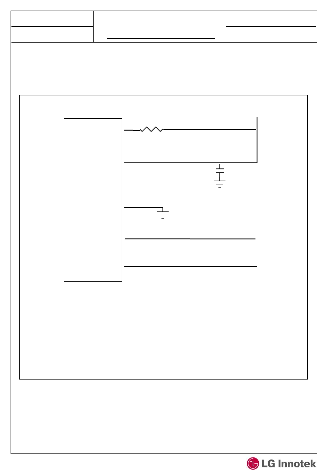
11. APPLICATION CIRCUIT
2.7 ~ 3.3V
1K ~ 3KΩ
1uF ~ 4.7uF
Dimming
Mode sel
VDD
GND
TWZT-V001D-F
On/off
S P E C I F I C A T I O N
PAGE :
REG. DATE :
MODEL NAME : TWZT-V001D-F
REV. DATE : . .
REV. NO. : 0.4 REG. DATE : 2014. 9. 17
REV. DATE : 2014 10 29 13 / 20
Copyrightⓒ. 2014. All Rights Reserved.
12. MODULE INTERFACE [ PIN DESCRIPTION ]
< Host Interface with PSU >
-. PWM
Mode
No.
I/O
Pin Name
Descrption
1 I Mode Sel
Low -> Test mode
2 - GPIO1 Reserved
3 - VDD Power Supply Typ. 3.0V (2.7V ~ 3.3V)
4 O
GPIO2 Reserved
5 - GND Ground
6 O
Dim Dimming Control
7 O
GPIO3 Reserved
8 O
On/off On/off Control
* Recommended Dimming & On/off Pin Initial State : Pull up
①
②
③
④ ⑤
⑥ ⑦ ⑧
S P E C I F I C A T I O N
PAGE :
REG. DATE :
MODEL NAME : TWZT-V001D-F
REV. DATE : . .
REV. NO. : 0.4 REG. DATE : 2014. 9. 17
REV. DATE : 2014 10 29 14 / 20
Copyrightⓒ. 2014. All Rights Reserved.
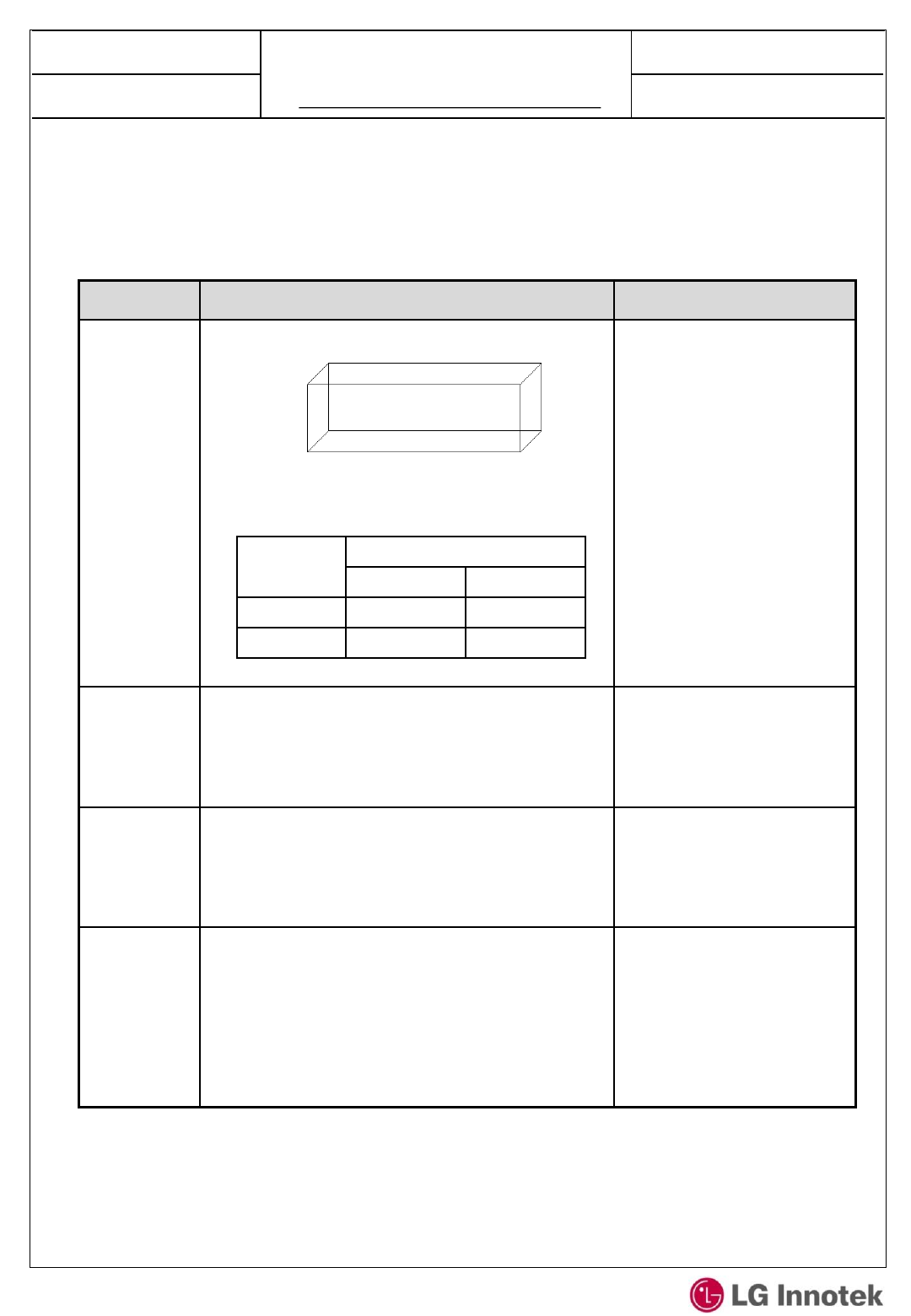
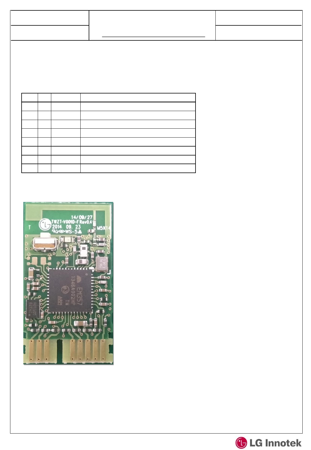
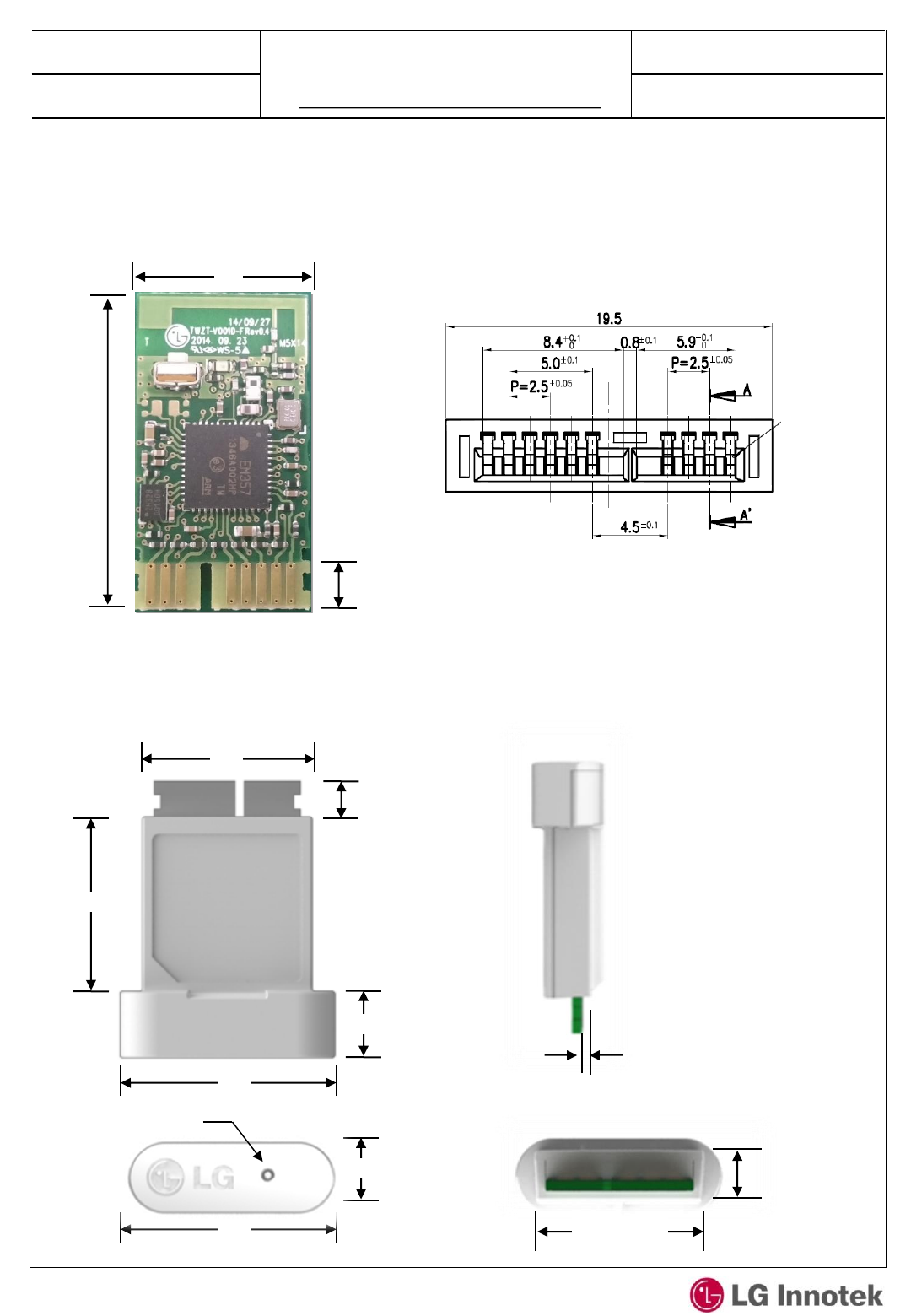
13. MECHANICAL INFORMATION
< MODULE PCB-A >
< Module Top Feature >
27.0
15.0
< Module Slot Dimension >
3.9
< CASE ASS’Y >
1.0±0.1
7.7
7.0
22.0
22.0
3.7
18.1
17.4
LED INDICATOR
17.4±0.1
5 ±0.2
S P E C I F I C A T I O N
PAGE :
REG. DATE :
MODEL NAME : TWZT-V001D-F
REV. DATE : . .
REV. NO. : 0.4 REG. DATE : 2014. 9. 17
REV. DATE : 2014 10 29 15 / 20
Copyrightⓒ. 2014. All Rights Reserved. 7 / 8
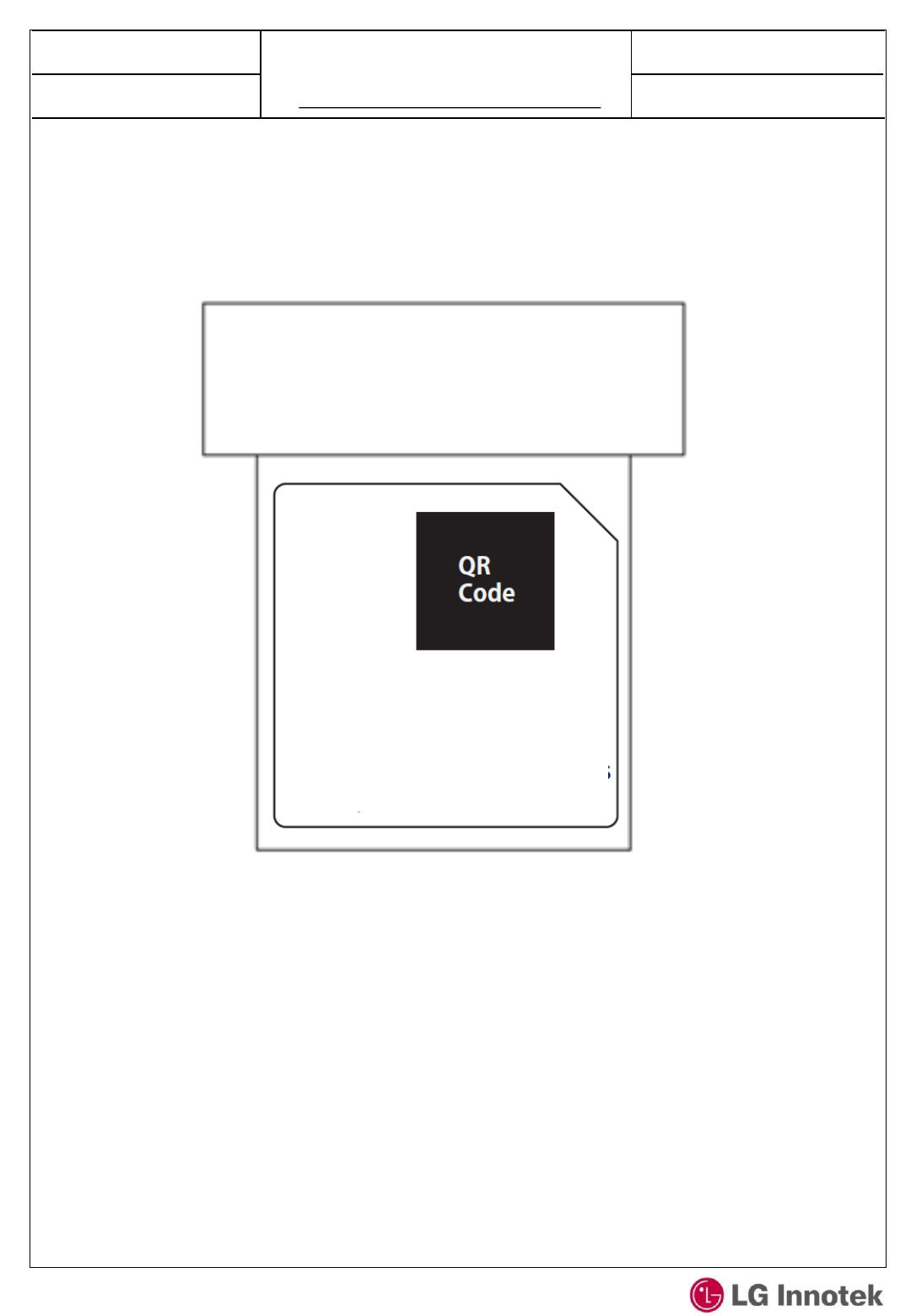
14. PRODUCT LABEL INFORMATION
FCC ID : YZP-TWZTV001D
IEEE Address : XXXXXXXX
xxxxXXXX
P/N :
TWZT
-V001D
S P E C I F I C A T I O N
PAGE :
REG. DATE :
MODEL NAME : TWZT-V001D-F
REV. DATE : . .
REV. NO. : 0.4 REG. DATE : 2014. 9. 17
REV. DATE : 2014 10 29 16 / 20
Copyrightⓒ. 2014. All Rights Reserved.
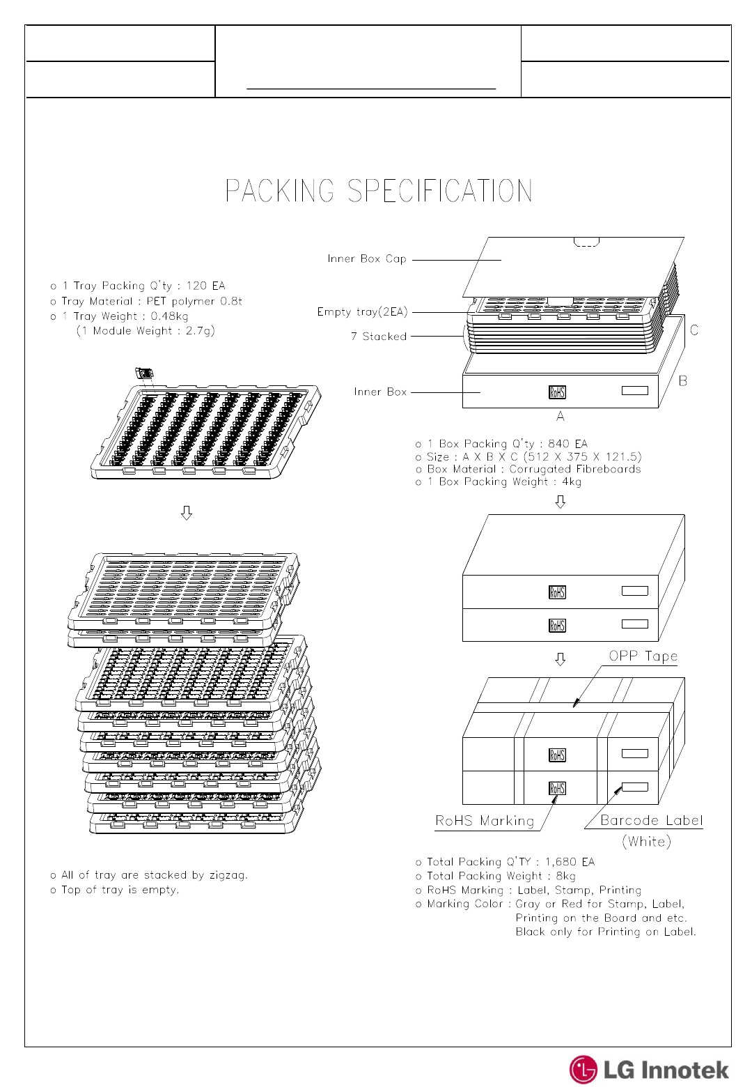
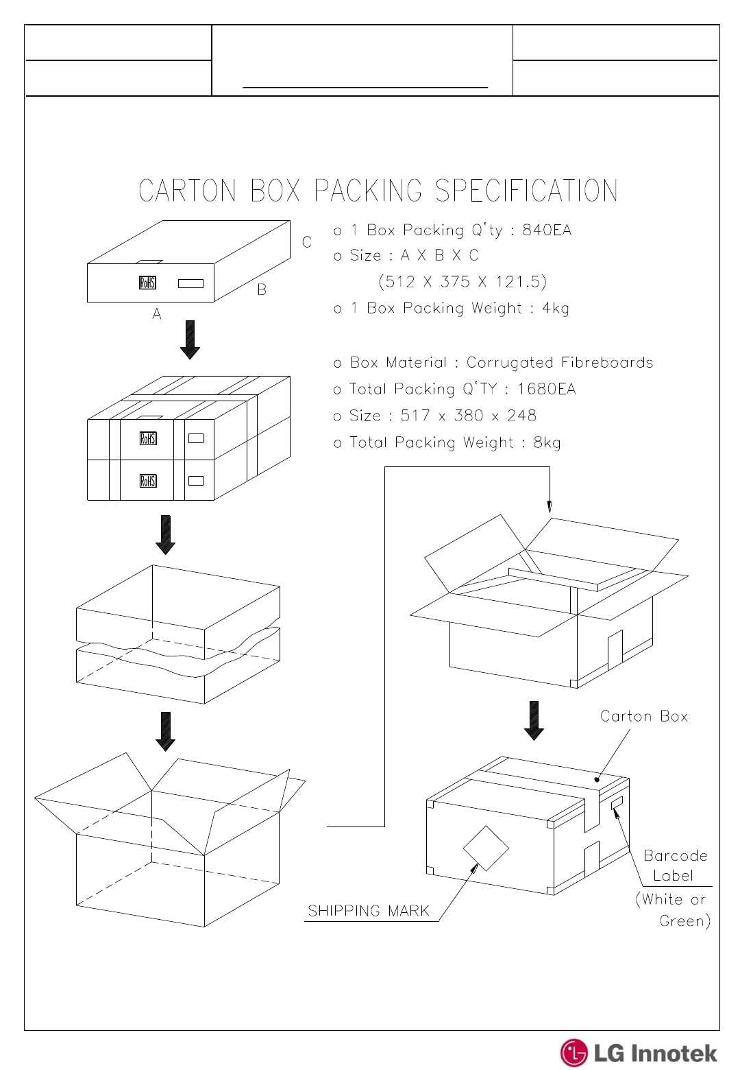
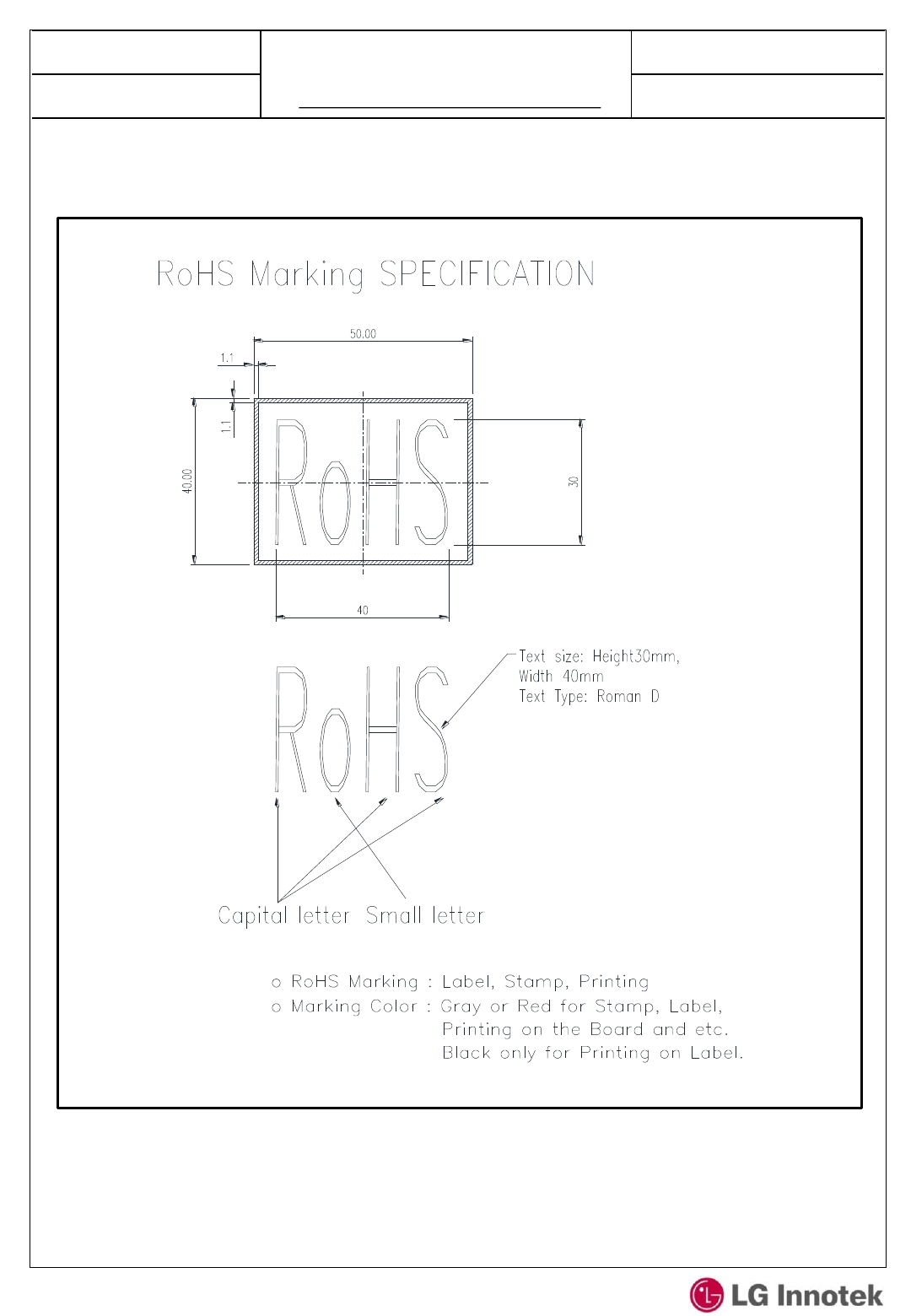
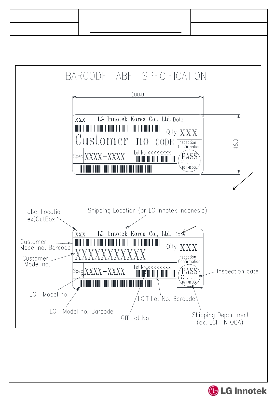
15. PACKING INFORMATION
S P E C I F I C A T I O N
PAGE :
REG. DATE :
MODEL NAME : TWZT-V001D-F
REV. DATE : . .
REV. NO. : 0.4 REG. DATE : 2014. 9. 17
REV. DATE : 2014 10 29 17 / 20
Copyrightⓒ. 2014. All Rights Reserved.
S P E C I F I C A T I O N
PAGE :
REG. DATE :
MODEL NAME : TWZT-V001D-F
REV. DATE : . .
REV. NO. : 0.4 REG. DATE : 2014. 9. 17
REV. DATE : 2014 10 29 18 / 20
Copyrightⓒ. 2014. All Rights Reserved.
S P E C I F I C A T I O N
PAGE :
REG. DATE :
MODEL NAME : TWZT-V001D-F
REV. DATE : . .
REV. NO. : 0.4 REG. DATE : 2014. 9. 17
REV. DATE : 2014 10 29 19 / 20
Copyrightⓒ. 2014. All Rights Reserved.
Date of production ( ex, 14.01.23 )
( 8-digit serial on date of production. Ex, 00000001 )
S P E C I F I C A T I O N
PAGE :
REG. DATE :
MODEL NAME : TWZT-V001D-F
REV. DATE : . .
REV. NO. : 0.4 REG. DATE : 2014. 9. 17
REV. DATE : 2014 10 29 20 / 20
Copyrightⓒ. 2014. All Rights Reserved.
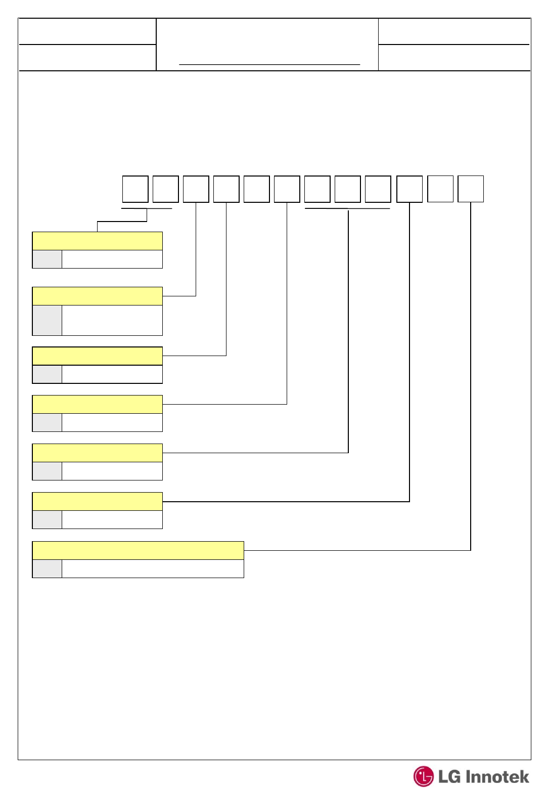
T
Mechanical Type
Stick
T W Z T - V 0 0 1 D
V
Chip Maker
Ember
001
Version
001
D
T/Rx Type
Duplex
Z
Module RF Type
Zigbee
TW
Product Type
Wireless Module
16. ORDERING INFORMATION
- F
F
Process
PCB Top Chip Mount Ass’y

FCC Information
This device complies with part 15 of the FCC Results. Operation is subject to the
following two conditions :
(1) This Device may not cause harmful interface, and
(2) This device must accept any interference received, including interference that
may cause undesired operation.
Note: This equipment has been tested and found to comply with the limits for CLASS B digital
device, pursuant to Part 15 of FCC Rules. These limits are designed to provide reasonable
protection against harmful interference when the equipment is operated in a commercial
environment This equipment generates, uses and can radiate radio frequency energy and, if not
installed and used in accordance with the instructions, may cause harmful interference to radio
communications. However, there is no guarantee that interference will not occur in a particular
installation. If this equipment does cause harmful interference to radio or television reception,
which can be determined by turning the equipment off and on, the user is encouraged to try
correct the interference by one or more of the following measures:
1.1. Reorient or relocate the receiving antenna.
1.2. Increase the separation between the equipment and receiver.
1.3. Connect the equipment into an outlet on a circuit different from that to which receiver is
connected.
1.4. Consult the dealer or experienced radio/TV technician for help.
WARNING
Changes or modifications not expressly approved by the manufacturer could void the
user’s authority to operate the equipment.
“CAUTION : Exposure to Radio Frequency Radiation.
Antenna shall be mounted in such a manner to minimize the potential for human
contact during normal operation. The antenna should not be contacted during operation
to avoid the possibility of exceeding the FCC radio frequency exposure limit.