LG Innotek VL1000 LTE/CDMA(EVDO) Wireless Modem Module User Manual 1
LG Innotek Co., Ltd. LTE/CDMA(EVDO) Wireless Modem Module 1
Contents
- 1. Manual
- 2. User manual 1 of 2
- 3. User manual 2 of 2
User manual 1 of 2
Copyright ⓒ. 2014. All Rights Reserved.
User Guide for LTD-VL1110 (Eagle)
1. Overview
2. Major feature
3. Interface
4. Electrical specification
5. RF specification
6. Mechanical specification
7. General specification
8. Connector
9. RFx information
10. FCC Approval
Table of Contents
Product : LTE/CDMA(EVDO) Wireless Modem
Model name : LTD-VL1110

Copyright ⓒ. 2014. All Rights Reserved.
The LTD-VL1110 is achieved as personal mobile communication devices of
the compact radio equipment, the latest design of the parts becoming smaller,
lighter weight having the LTE(700/1700MHz), CDMA(850/1900MHz) bands. It is
the vehicle’s telematics system that connect with LTE and CDMA(EVDO)
wireless network and the wireless module with voice and data communication. It
can be operated at land, rivers, and other similar areas.
On LTE operating mode, It can be communicated with uplink 50Mbps, downlink
up to 100Mbps data transfer speed such as a movie or a video call. It may be
able to receive large amounts of data.
Standard RS-232 port and USB port communicating with the host system via
AT-command or control commands can be used to send data. Voice calls are
possible.
1. Overview
Copyright ⓒ. 2014. All Rights Reserved.
Mechanical
Dimension
93.15(L) x 45.0(W) x 7.6(T) mm
Weight
45g(max)
Interface
USB, UART, General Purpose I/O pins
Antenna
FAKRA Connector
Temperature *
Operation : -20℃ ~ +70 ℃
Storage : -40 ℃ ~ +85 ℃
Technology
Main Chipset
MDM 9615
Memory
2048Mb(NAND) / 1024Mb(SDRAM)
Standard
3GPP Rel.8 LTE Cat.3
- DL Speed : 100 Mbps(20M bandwidth)
- UL Speed : 50 Mbps(20M bandwidth)
3GPP2 CDMA 1X, EVDO Rev.A
- DL Speed : 3.1 Mbps
- UL Speed : 1.8 Mbps
Band
LTE B4, B13
CDMA 850(Cellular), 1900 (PCS)
GPS Not Supported
Power
LTE : Typ. 23dBm(Power Class 3)
CDMA : Typ. 24dBm (Power Class 3)
ETC
DC Power
3.8V
Functions
Voice, Data, SMS
2. Major feature
Copyright ⓒ. 2014. All Rights Reserved.
3. Interface
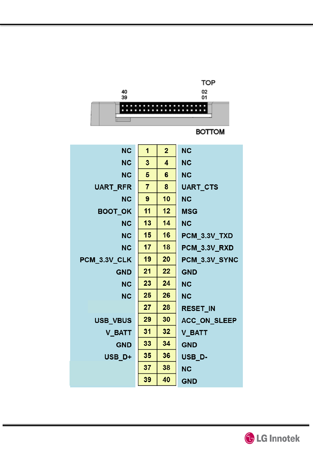
Customer P/N is connected with outer device using 40 pin connector
3.1 Pin output
Figure 1. Connector pin arrangement
48H_END
UART_TX_TCU
UART_RX_TCU
Copyright ⓒ. 2014. All Rights Reserved.
3. Interface
3.2 Pin description
Pin NO. Signal Name In/Out Function
NC
1, 2, 3, 4, 5, 6, 9,
10, 13, 14, 15, 17
, 23, 24, 25, 26, 3
8
NC
V_BATT 31, 32 POWER POWER
GND 21, 22, 33, 34, 40
GND GND
Audio
PCM
16 PCM_3.3V_TXD O PCM DATA OUT
18 PCM_3.3V_RXD I PCM DATA IN
19 PCM_3.3V_CLK I PCM CLK
20 PCM_3.3V_SYNC
I PCM SYNC
UART2
(DM Port)
37 UART_RXD I UART RX DATA
39 UART_TXD O UART TX DATA
7 UART_RFR O UART ready-for-receive
8 UART_CTS I UART clear-to-send
USB
(USB2.0)
29 USB_VBUS I Power supply for the
USB transceiver
35 USB_D+ I/O USB differential data (+)
36 USB_D- I/O USB differential data (-)
User Interface
11 BOOT_OK O Modem Booting Completion
/ Modem Wake Up
12 MSG O Received emergency
message from Center
27 96H_END O Signified in 96 hours
standby mode ending
28 RESET_IN I Modem Hardware reset
input
30 ACC_ON_SLEEP
I Modem Power ON
/ Modem POWER Sleep
Table 1. Pin descriptions
Copyright ⓒ. 2014. All Rights Reserved.
3. Interface
3.3 UART(RS-232 Interface)
This module is provided with interface supporting Standard RS-232 protocol.
DCE(modem) communicate with DTE(host) through data or control AT-
Command.
Pin No. Signal Name Direction Function
37 UART_RXD I UART RX DATA
39 UART_TXD O UART TX DATA
7 UART_RFR O UART ready-for-receive
8 UART_CTS I UART clear-to-send
3.4 USB
It is supported with universal serial bus for high data communication. And It
is satisfied with USB2.0 specification and supported with max.480Mbps
Pin No. Signal Name Direction Function
37 UART_RXD I UART RX DATA
39 UART_TXD O UART TX DATA
7 UART_RFR O UART ready-for-receive
8 UART_CTS I UART clear-to-send
Table 2. UART Pin descriptions
Table 3. USB Pin descriptions
Copyright ⓒ. 2014. All Rights Reserved.
3. Interface
3.5 Audio
This module is provided with PCM interface. The resistor of pulled-up or
pulled-down in this pin must be over 50Kohm.
Pin No. Signal Name Direction Function
37 UART_RXD I UART RX DATA
39 UART_TXD O UART TX DATA
7 UART_RFR O UART ready-for-receive
8 UART_CTS I UART clear-to-send
Table 4. PCM Pin descriptions
3.6 User interface
Pin No. Signal Name Direction Function
11 BOOT_OK O Modem booting end
/ Modem Wake Up
12 MSG O Received emergency message
from center
27 96H_END O Signified in 96 hours standby
mode ending
28 RESET_IN- I Modem Hardware reset input
30 ACC_ON_SLEEP I Modem Power ON
/ Modem Power Sleep
Table 5. User interface Pin descriptions
Copyright ⓒ. 2014. All Rights Reserved.
4. Electrical specification
4.1 Power supply specification
Modem power(V_BATT) should be provided DC3.8V ± 0.1V, 2.0A. Modem
power is provided according to inner function and per block using DC
regulated circuit. It is controlled with each power depending on the
mechanism to reduce power consumption to a minimum. PA is used directly
V_BATT because of a lot of power input power source. Thus, It can be
resulted in breakage of PA in excess of the rated input power. In addition,
surge and ESD should be designed to block the influx in order to prevent
damage to the modem.
Pin No. Signal Name Direction MIN TYP MAX
32, 33 V_BATT I 3.7V 3.8V 3.9V
Table 6. Power supply specification
Copyright ⓒ. 2014. All Rights Reserved.
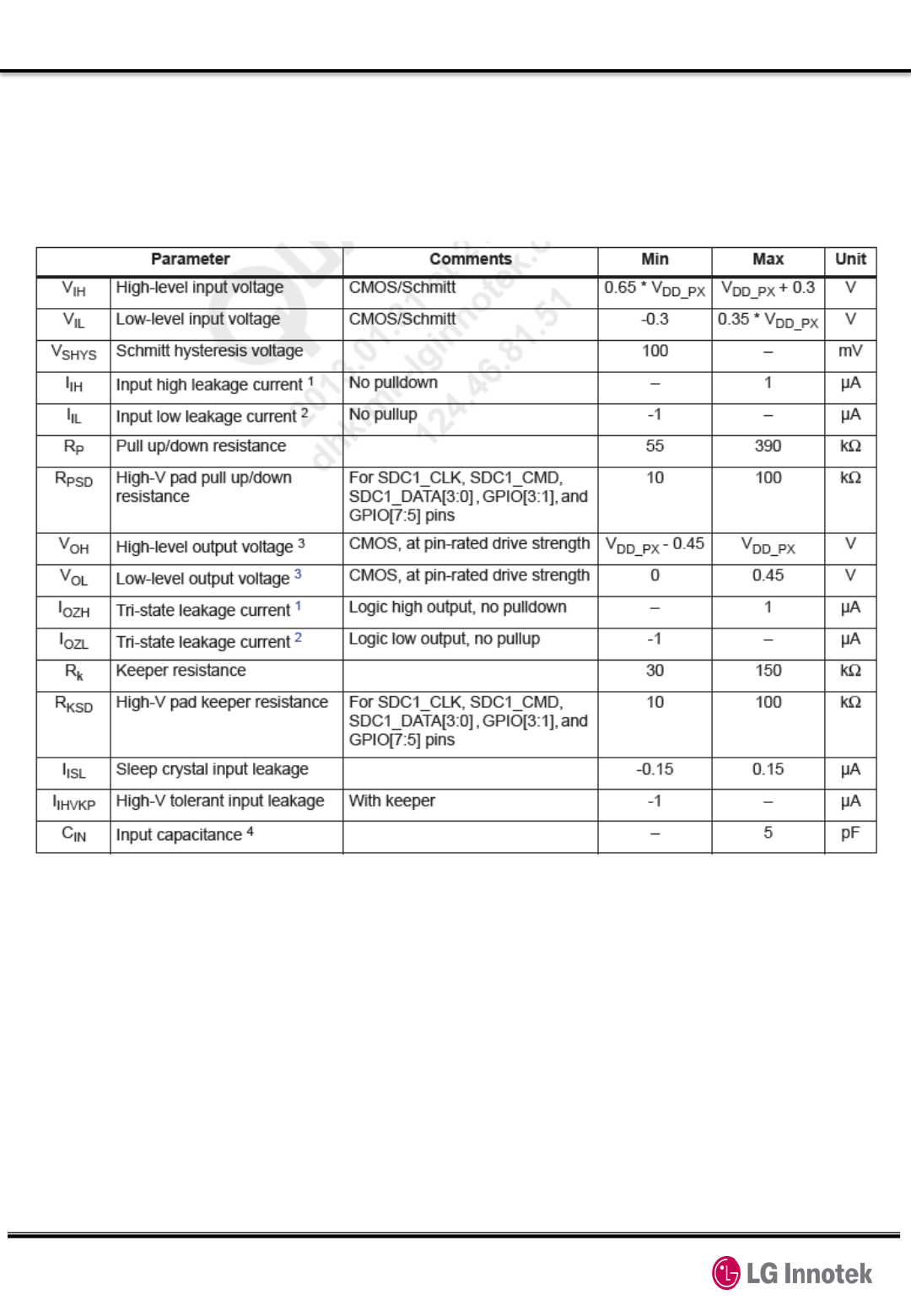
4. Electrical specification
4.2 Logic level specification
4.2.1 Digital logic level specification
Basic interface level : CMOS 1.8V
Table 7. Digital logic level specification

Copyright ⓒ. 2014. All Rights Reserved.
5. RF specification
5.1 CDMA
5.1.1 Receiver
.- Bandwidth : 1.25MHz
.- Frequency : 869MHz – 894MHz (BC0), 1930MHz – 1990MHz (BC1)
.- RF to Baseband Direct conversion (Zero IF)
.- Modulation method : QPSK, 8PSK and 16QAM
.- Sensitivity : ≤-104dBm (BER = Under 0.5%)
5.1.2 Transmitter
.- Frequency: 824MHz – 849MHz (BC0), 1850MHz – 1910MHz (BC1)
.- Maximum RF Output : Power class3 (BC0), 23.01dBm ~ 26dBm
Power class2 (BC1), 23.01dBm ~ 26dBm
.- Modulation method : BPSK, QPSK AND 8PSK
.- Baseband to RF Direct conversion (Zero IF)
5.2 LTE
5.2.1 Receiver
.- Bandwidth : B4(20MHz), B13(10MHz)
.- Frequency : 2110MHz – 2155MHz (B4), 746MHz – 756MHz (B13)
.- RF to Baseband Direct conversion (Zero IF)
.- Modulation method : QPSK, 16QAM and 64QAM
.- 수신감도 : Main - B4 (≤-93.3dBm @QPSK), B13(≤-93.3dBm @QPSK)
Diversity - B4 (≤-93.3dBm @QPSK), B13(≤-93.3dBm @QPSK)
5.2.2 Transmitter
.- Frequency : B4 (1710MHz – 1755MHz), B13(777MHz – 787MHz)
.- Maximum RF Output : Power class 3, 20.3dBm ~ 25.7dBm
.- Modulation method : QPSK and 16QAM
.- Baseband to RF Direct conversion (Zero IF)
Copyright ⓒ. 2014. All Rights Reserved.
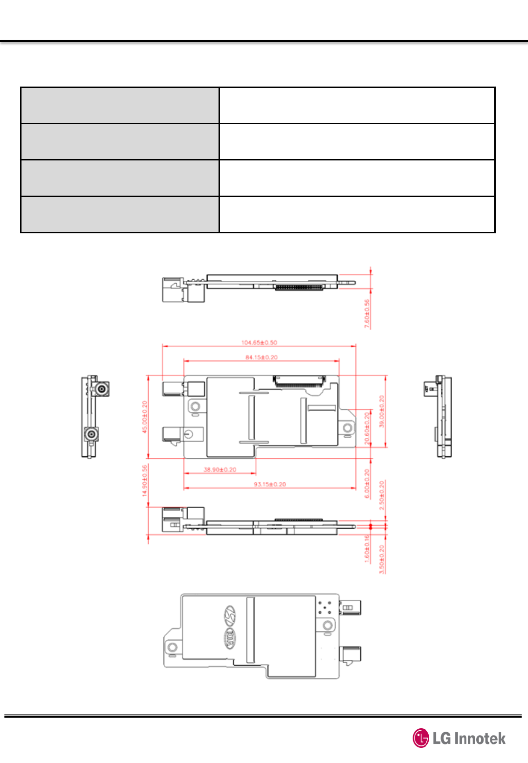
6. Mechanical specification
6.1 Mechanical dimensions
Dimensions 93.15 x 45.0 x 7.6 mm
Weight 45 grams(max.)
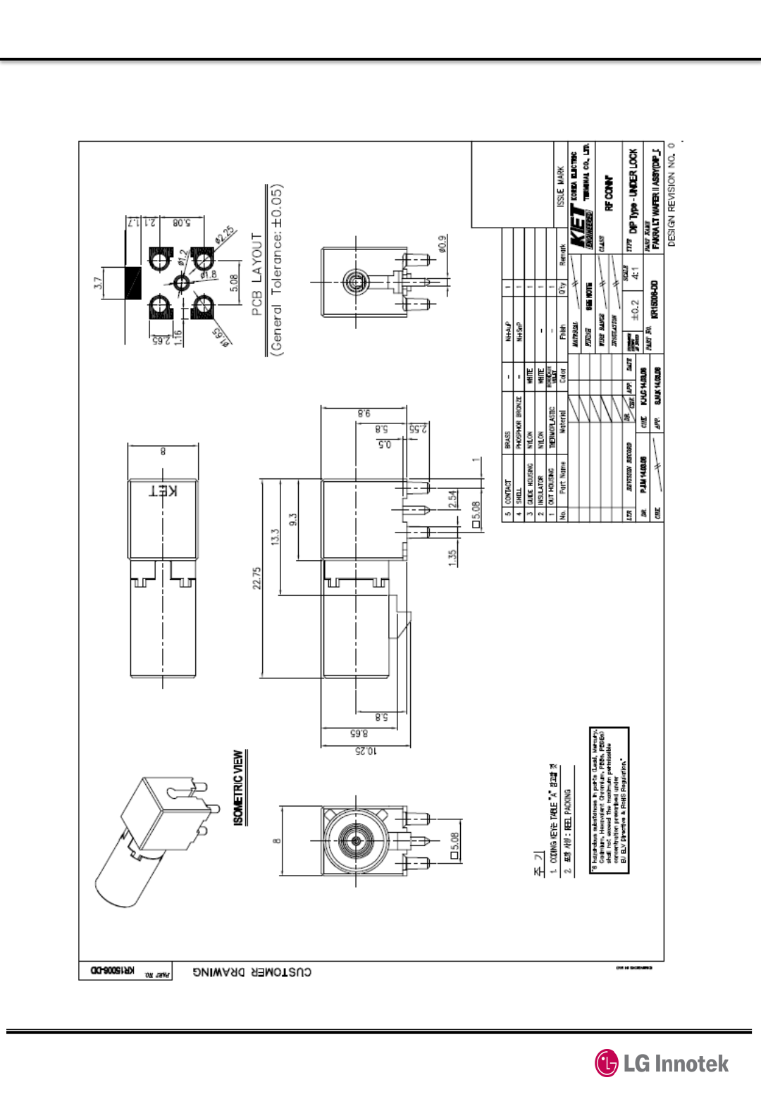
Modem Interface connector KM17E-40DS (Vendor : HIROSE)
Modem Antenna Connector (Plug) Main Antenna : KR15006-DD (Vendor : KET)
Diversity Antenna : KR15003-SG (Vendor : KET)
Table 8. Mechanical specification
Figure 2. Mechanical dimension

Copyright ⓒ. 2014. All Rights Reserved.
6. Mechanical specification
6.1 Environment specification
.- Storage Temp : -40℃ ~ +85℃
.- Operating Temp : -20℃ ~ +70℃
(-20℃ ~ +70℃ : 3GPP specifications are satisfied
-30℃~-20℃, +70℃~+80℃ : It can be performance degradation)
.- Operating humidity : 80% (60℃) relative humidity
Copyright ⓒ. 2014. All Rights Reserved.
7. General specification
7.1 CDMA electrical specification
Test item Spec.
CHANNEL
1011/25
384/600
779/1175
4.4.5 Maximum Output Power 23.01~26dBm PASS PASS PASS
4.5.1 Conducted Spurious
Emissions
885 kHz to
1.98 MHz -42 dBc↓/30 kHz PASS PASS PASS
1.98 MHz to
4.00 MHz -54 dBc↓/30 kHz (BC0)
-50 dBc↓/30 kHz (BC1) PASS PASS PASS
4.4.6 Minimum Controlled Output Power -50dBm↓ PASS PASS PASS
4.3.4 Waveform Quality
Rho 0.94 ~1.00 PASS PASS PASS
Freq_E +/-300.00Hz(BC0)
+/-150.00Hz(BC1) PASS PASS PASS
Time_E -1.00~1.00 us PASS PASS PASS
4.4.4
Range of Closed Loop
Power Control
up @ Full rate
24↑ PASS PASS PASS
down @ Full
Rate -24↓ PASS PASS PASS
up @ Half
rate 24↑ PASS PASS PASS
down @ Half
Rate -24↓ PASS PASS PASS
up @ Quarter
rate 24↑ PASS PASS PASS
down @
Quarter Rate
-24↓ PASS PASS PASS
up @ Eighth
rate 24↑ PASS PASS PASS
down @
Eighth Rate -24↓ PASS PASS PASS
4.4.2 Time Response of Open Loop Control
PASS PASS PASS PASS
4.4.1
Range of Open Loop
Power
Open Loop
Power Upper
-57.50~-38.50(BC0)
-60.50~-41.50(BC1) PASS PASS PASS
Open Loop
Power Mid -17.50~1.50(BC0)
-20.50~-1.50(BC1) PASS PASS PASS
Open Loop
Power Sense
10.50~29.50(BC0)
10.50~29.50(BC1) PASS PASS PASS
3.5.1 Reference Sensitivity Level(-104/-25) 0.5%↓ PASS PASS PASS
Table 9. CDMA RF specification

Copyright ⓒ. 2014. All Rights Reserved.
7. General specification
7.2 LTE B4(20M) electrical specification
Table 10. LTE B4(20M) RF specification
시험 항목 Spec. Test Temperature
Channel
2050
2175
2300
6.2.2 Maximum Output Power(class 3) 23±2.7dBm Normal, Temp L,
Temp H
PASS
PASS
PASS
6.3.2 Minimum Output Power -39dBm ↓ Normal, Temp L,
Temp H
PASS
PASS
PASS
6.5.1 Frequency Error ±0.1ppm Normal, Temp L,
Temp H
PASS
PASS
PASS
6.5.2.1
Error Vector Magnitude(EVM)
17.5%↓
(QPSK) Normal
PASS
PASS
PASS
12.5%↓
(16QAM)
PASS
PASS
PASS
6.5.2.2
Relative Carrier
Leakage Power
Carrier Leakage
(3.2dBm ± 3.2dB) -27.2 dBc
Normal, Temp L,
Temp H
PASS
PASS
PASS
Carrier Leakage
(-26.8dBm ± 3.2dB) -19.2 dBc
PASS
PASS
PASS
Carrier Leakage
(-36.8dBm ± 3.2dB) -9.2 dBc
PASS
PASS
PASS
6.5.2.4
EVM equalizer
spectrum flatness
EVM equalizer spectrum
flatness Range1 5.4 dB ↓ Normal, Temp L,
Temp H
PASS
PASS
PASS
EVM equalizer spectrum
flatness Range2 9.4 dB ↓
PASS
PASS
PASS
6.6.1 Occupied Bandwidth (OBW) 20 MHz ↓ Normal
PASS
PASS
PASS
6.6.2.1
Spectrum emission
mask
Spectrum Emission Mask
upper/lower Area 1 -19.5 dBm ↓
Normal
PASS
PASS
PASS
Spectrum Emission Mask
upper/lower Area 2 -8.5 dBm ↓
PASS
PASS
PASS
Spectrum Emission Mask
upper/lower Area 3 -11.5 dBm ↓
PASS
PASS
PASS
Spectrum Emission Mask
upper/lower Area 4 -23.5 dBm ↓
PASS
PASS
PASS
6.6.2.3
Adjacent Channel
Leakage Power Ratio
(ACLR)
ACLR E-UTRA ± -29.2dB ↓
Normal, Temp L,
Temp H
PASS
PASS
PASS
ACLR UTRA Offset 1 ± -32.2dB ↓
PASS
PASS
PASS
ACLR UTRA Offset 2 ± -35.2dB ↓
PASS
PASS
PASS
7.3
Reference Sensitivity
Level @ 20MHz
Main Ref Sense throughput
shall be ≥ 95% -93.3 dBm Normal, Temp L,
Temp H
PASS
PASS
PASS
Div. Ref Sense throughput
shall be ≥ 95% -93.3 dBm
PASS
PASS
PASS
7.4 Maximum Input Level
throughput shall be ≥ 95% -25.7 dBm Normal
PASS
PASS
PASS
Copyright ⓒ. 2014. All Rights Reserved.
7. General specification
7.3 LTE B13(10M) electrical specification
Table 11. LTE B13(10M) RF specification
시험 항목 Spec. Test Temperature
Channel
2050
2175
2300
6.2.2 Maximum Output Power(class 3) 23±2.7dBm Normal, Temp L,
Temp H
PASS
PASS
PASS
6.3.2 Minimum Output Power -39dBm ↓ Normal, Temp L,
Temp H
PASS
PASS
PASS
6.5.1 Frequency Error ±0.1ppm Normal, Temp L,
Temp H
PASS
PASS
PASS
6.5.2.1
Error Vector Magnitude(EVM)
17.5%↓
(QPSK) Normal
PASS
PASS
PASS
12.5%↓
(16QAM)
PASS
PASS
PASS
6.5.2.2
Relative Carrier
Leakage Power
Carrier Leakage
(3.2dBm ± 3.2dB) -27.2 dBc
Normal, Temp L,
Temp H
PASS
PASS
PASS
Carrier Leakage
(-26.8dBm ± 3.2dB) -19.2 dBc
PASS
PASS
PASS
Carrier Leakage
(-36.8dBm ± 3.2dB) -9.2 dBc
PASS
PASS
PASS
6.5.2.4
EVM equalizer
spectrum flatness
EVM equalizer spectrum
flatness Range1 5.4 dB ↓ Normal, Temp L,
Temp H
PASS
PASS
PASS
EVM equalizer spectrum
flatness Range2 9.4 dB ↓
PASS
PASS
PASS
6.6.1 Occupied Bandwidth (OBW) 10 MHz ↓ Normal
PASS
PASS
PASS
6.6.2.1
Spectrum emission
mask
Spectrum Emission Mask
upper/lower Area 1 -16.5 dBm ↓
Normal
PASS
PASS
PASS
Spectrum Emission Mask
upper/lower Area 2 -8.5 dBm ↓
PASS
PASS
PASS
Spectrum Emission Mask
upper/lower Area 3 -11.5 dBm ↓
PASS
PASS
PASS
Spectrum Emission Mask
upper/lower Area 4 -23.5 dBm ↓
PASS
PASS
PASS
6.6.2.3
Adjacent Channel
Leakage Power Ratio
(ACLR)
ACLR E-UTRA ± -29.2dB ↓
Normal, Temp L,
Temp H
PASS
PASS
PASS
ACLR UTRA Offset 1 ± -32.2dB ↓
PASS
PASS
PASS
ACLR UTRA Offset 2 ± -35.2dB ↓
PASS
PASS
PASS
7.3
Reference Sensitivity
Level @ 10MHz
Main Ref Sense throughput
shall be ≥ 95% -93.3 dBm Normal, Temp L,
Temp H
PASS
PASS
PASS
Div. Ref Sense throughput
shall be ≥ 95% -93.3 dBm
PASS
PASS
PASS
7.4 Maximum Input Level
throughput shall be ≥ 95% -25.7 dBm Normal
PASS
PASS
PASS
Copyright ⓒ. 2014. All Rights Reserved.
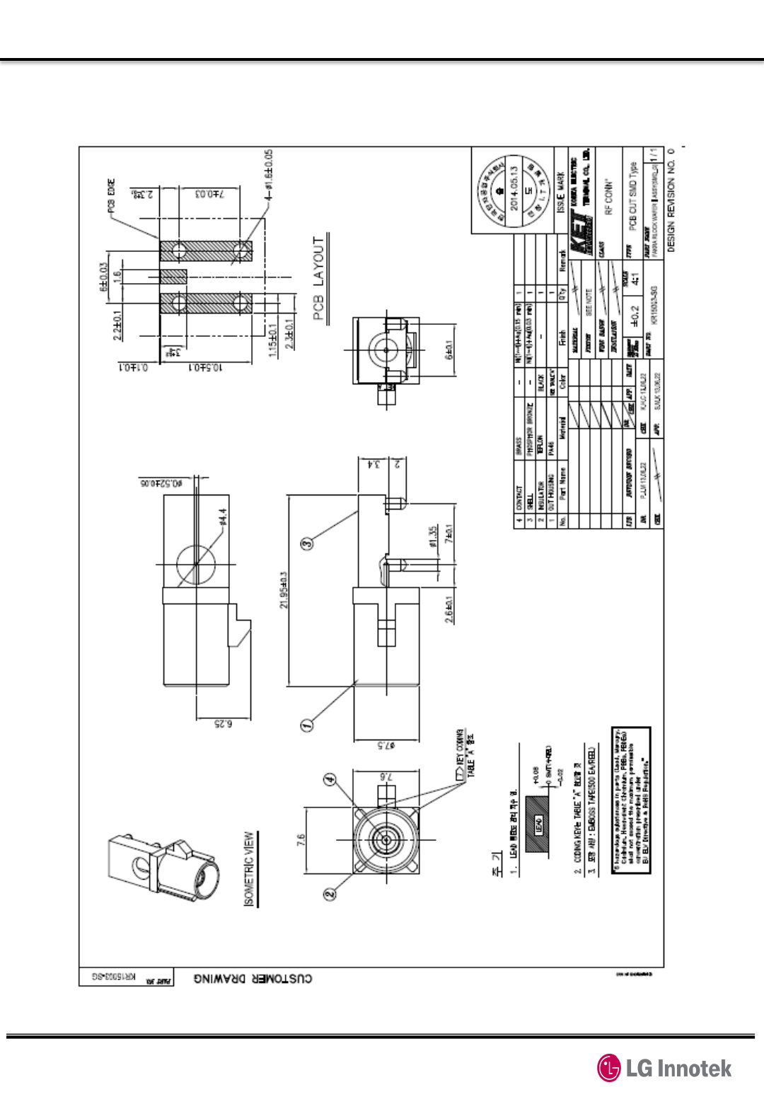
8. Connector
8.1 Antenna Connector(Main): KR15006-DD (Vendor : KET)
Copyright ⓒ. 2014. All Rights Reserved.
8. Connector
8.2 Antenna Connector(Div.) KR15003-SG (Vendor : KET)
Copyright ⓒ. 2014. All Rights Reserved.
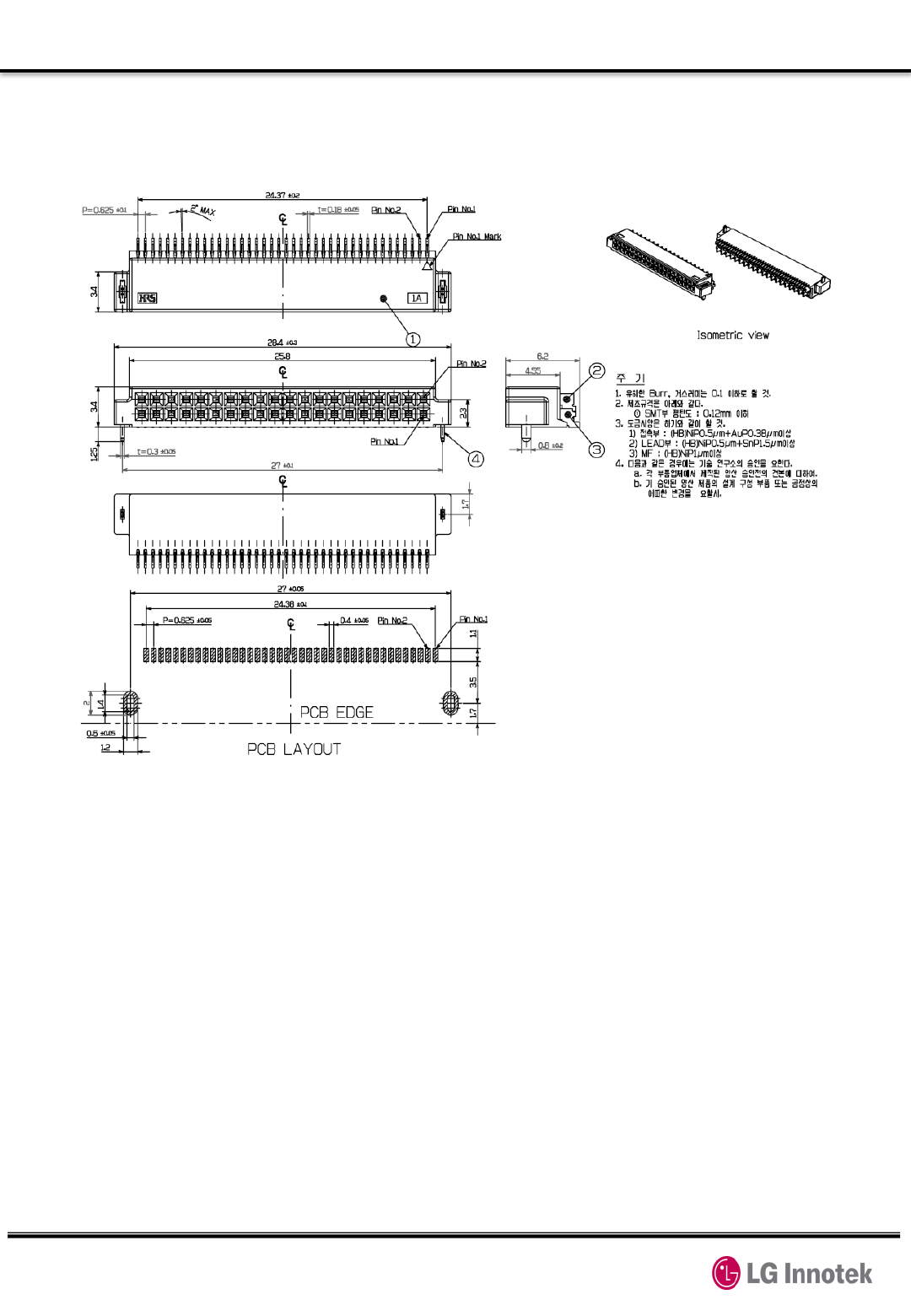
8. Connector
8.3 40Pin Connector : KM17E-40DS (Vendor : HIROSE)

Copyright ⓒ. 2014. All Rights Reserved.
9. RFx Information
The RF field strength of the wireless module or modules that may be
embedded in your TCU is well all international RF exposure limits as known
at this time. Because the wireless modules(which may be embedded into your
TCU) emit less energy than is allowed in radio frequency safety standards and
recommendations, manufacturer believes these modules are safe for use.
Regardless of the power levels, care should be taken to minimize human
contact during normal operation. This module should be used more than 20cm(8
inches) from the body when wireless devices are on and transmitting.
This transmitter must not be collocated or operate in conjunction with any other
antenna or transmitter. Operation is subject to the following two conditions: (1)
this module may not cause interference , (2) this module must accept any
interference that may cause undesired operation.
10.1 Information for integrator
The integrator has to be aware not to provide information to the end user
regarding how to install or remove this RF module in the user manual of the end
product. The user manual which is provided by integrators for end users must
include the following information in a prominent location. To comply with FCC RF
exposure compliance requirements, the antenna used for this transmitter must
be installed to provide a separation distance of at least 20cm from all persons
and must not be collocated or operating in conjunction with any other antenna or
transmitter. Label for end product must include contains FCC ID : YZP-VL1000
or A RF transmitter inside, FCC ID : YZP-VL1000
Copyright ⓒ. 2014. All Rights Reserved.
10. FCC Approval
This Module complies with parts 22, 24, 27 of the FCC rules.
This device complies with FCC radiation exposure limits set forth for an
uncontrolled environment.
This module should be installed and operated with minimum distance 20cm
between the radiating element of this device and the user.
This module may not be co-located with any other transmitters or antennas.
To comply with FCC regulations limiting both maximum RF output power and
human exposure to RF radiation, the maximum antenna gain including cable
loss in a mobile-only exposure condition must not exceed the table below.
Band Frequency Range
[MHz] Maximum Antenna
Gain[dBi]
CDMA(Cellular) 824.70~848.31
CDMA(PCS) 1851.25~1908.75
LTE(B13) 779.50~874.50
LTE(B4) 1710.70~1754.30
The satisfy FCC exterior labeling requirements, the following text must be placed
on the exterior of the end product.
Contains Transmitter module FCC ID: YZP-VL1000
Changes or modifications to this equipment may cause harmful interference
unless the modifications are expressly approved in the instruction manual. The
user could lose the authority to operate this equipment if an unauthorized
change or codification is made.
Note: If this module is intended for use in a portable device, additional testing
will be required to satisfy RF Exposure, including SAR requirements of FCC Part
2.1093.
5.50
7.00
5.31
4.29