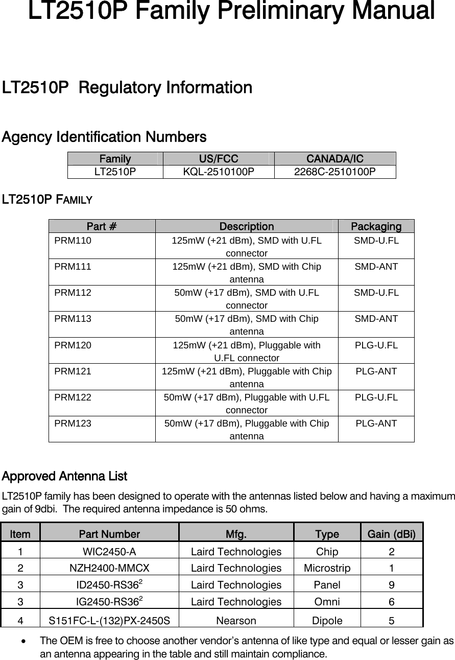
Laird Connectivity 2510100P FREQUENCY HOPPING SPREAD SPECTRUM TRANSCEIVER User Manual

AeroComm Corporation FREQUENCY HOPPING SPREAD SPECTRUM TRANSCEIVER Users Manual

Users Manual

LT2510P Family Preliminary Manual   LT2510P  Regulatory Information  Agency Identification Numbers Family   US/FCC  CANADA/IC LT2510P KQL-2510100P 2268C-2510100P LT2510P FAMILY  Part #  Description  Packaging PRM110 125mW (+21 dBm), SMD with U.FL connectorSMD-U.FLPRM111 125mW (+21 dBm), SMD with Chip antennaSMD-ANTPRM112 50mW (+17 dBm), SMD with U.FL connectorSMD-U.FLPRM113 50mW (+17 dBm), SMD with Chip antennaSMD-ANTPRM120 125mW (+21 dBm), Pluggable with U.FL connectorPLG-U.FLPRM121 125mW (+21 dBm), Pluggable with Chip antennaPLG-ANTPRM122 50mW (+17 dBm), Pluggable with U.FL connectorPLG-U.FLPRM123 50mW (+17 dBm), Pluggable with Chip antennaPLG-ANT Approved Antenna List LT2510P family has been designed to operate with the antennas listed below and having a maximum gain of 9dbi.  The required antenna impedance is 50 ohms. Item  Part Number  Mfg.  Type  Gain (dBi) 1 WIC2450-A Laird Technologies Chip 2 2 NZH2400-MMCX Laird Technologies Microstrip 1 3 ID2450-RS362Laird Technologies  Panel  9 3 IG2450-RS362Laird Technologies  Omni  6 4 S151FC-L-(132)PX-2450S  Nearson  Dipole  5 •  The OEM is free to choose another vendor’s antenna of like type and equal or lesser gain as an antenna appearing in the table and still maintain compliance.
FCC/ IC REQUIREMENTS FOR MODULAR APPROVAL In general, there are two agency classifications of wireless applications; portable and mobile. Portable – Portable is a classification of equipment where the user, in general, will be within 20 cm of the transmitting antenna. Portable equipment is further broken down into two classes; within 2.5 cm of human contact and beyond 2.5 cm. The LT2510P family is not agency approved for portable applications. The OEM is required to have additional testing performed to receive this classification. Contact Laird Technology for more details. Mobile – Mobile defines equipment where the user will be 20 cm or greater from the transmitting equipment. The antenna must be mounted in such a way that it cannot be moved closer to the user with respect to the equipment, although the equipment may be moved. This equipment has been approved for mobile applications where the equipment should be used at distances greater than 20 cm from the human body. Operation at distances of less than 20 cm would require additional RF exposure evaluation, including SAR requirement according to FCC RF Exposure guideline.   NOTE: This equipment has been tested and found to comply with the limits for a Class B digital device, pursuant to Part 15 of the FCC Rules. These limits are designed to provide reasonable protection against harmful interference in a residential installation. This equipment generates, uses and can radiate radio frequency energy and, if not installed and used in accordance with the instructions, may cause harmful interference to radio communications. However, there is no guarantee that interference will not occur in a particular installation. If this equipment does not cause harmful interference to radio or television reception, which can be determined by turning the equipment off and on, the user in encouraged to try to correct the interference by one or more of the following measures: •  Re-orient or relocate the receiving antenna •  Increase the separation between the equipment and the receiver •  Connect the equipment to an outlet on a circuit that is different from that to which the receiver is connected. •  Consult the dealer or an experienced radio/TV technician for help.   OEM EQUIPMENT LABELING REQUIREMENTS  WARNING: The OEM must ensure that FCC labeling requirements are met. This includes a clearly visible label on the outside of the OEM enclosure specifying the appropriate Laird Technology FCC identifier for this product as well as the FCC notice below. The FCC identifiers are listed above.  Contains FCC ID:KQL-2510100P This enclosed device complies with Part 15 of the FCC Rules, Operation is subject to the following two conditions: (1) This device may not cause harmful interference, and (2) This device must accept any interference received, including interference that may cause undesired operation Label and text information should be in a size of type large enough to be readily legible, consistent with the dimensions of the equipment and the label. However, the type size for the text is not required to be larger than eight point.
ANTENNA REQUIREMENTS To reduce potential radio interference to other users, the antenna type and gain should be chosen so that the equivalent isotropically radiated power (e.i.r.p.) is not more than that permitted for successful communication. WARNING: This device has been tested with an U.FL connector and the above listed antennas. When integrated into the OEM’s product, these fixed antennas require professional installation preventing end-users from replacing them with non-approved antennas. Any antenna not listed in the above table must be tested to comply with FCC Section 15.203 for unique antenna connectors and Section 15.247 for emissions. Contact Laird Technology for assistance. Caution: Any changes or modifications not expressly approved by Laird Technology could void the user’s authority to operate the equipment.  WARNINGS REQUIRED IN OEM MANUALS WARNING: This equipment has been approved for mobile applications where the equipment should be used at distances greater than 20cm from the human body. Operation at distances of less than 20cm is prohibited and requires additional SAR evaluation .
2   www.lairdtech.com  Laird Technologies  LT2510 Wireless ModuleKEY FEATURES•  Retries and acknowledgements•   Congurable network parameters•   Multiple generic I/O•   280 kbps or 500kbps RF data stream•   Idle current draw of 12mA, sleep current of 50uA•   Software selectable interface baud rates from 1200 bps to 460.8 kbps•   Upgradable FW through serial portThe LT2510 Frequency Hopping Spread Spectrum Transceiver Module from Laird Technologies is the latest in robust and easy to use radio modules. Supporting both high data rates and long ranges, the LT2510 is a great t for any number of machine to-machine applications. The LT2510 features an easy to use serial UART with hardware ow control for fast integration into an existing serial infrastructure.•   Low cost, low power and small size ideal for high volume, portable and battery powered applications•   All modules are qualied for Industrial temperatures (-40°C to 85°C)•   Advanced conguration available using AT commands•   Easy to use Conguration & Test Utility softwareOVERVIEW The LT2510 is available in two main versions, one with 100mW conducted output power and approved for North American and similar markets and one with 50mW conducted output power and approved for European and similar markets. These modules are identical except for output power, max power consumption, and the number of RF Channels available. This document will call out the differences where appropriate based on the part numbers. This document contains information about the hardware and software interface between a Laird Technologies LT2510 transceiver and an OEM Host. Information includes the theory of operation, specications, interface denitions, conguration information and mechanical drawings.Note: Unless mentioned specically by name, the LT2510 modules will be referred to as “radio” or “transceiver”. Individual naming is used to differentiate product specic features. The host (PC/Microcontroller/Any device to which the LT2510 module is connected) will be referred to as “OEM Host” or “Host.”OVERVIEW AND KEY FEATURES
3   www.lairdtech.com  Laird Technologies  LT2510 Wireless ModuleTABLE 1: LT2510 DETAILED SPECIFICATIONSGENERAL FCC: PRM110/111/120/121 CE: PRM112/113/122/123Form Factor SMD-ANT, SMD-U.FL, Pluggable-ANT, Pluggable-U.FLAntenna Integrated chip antenna or external antenna through U.FL connectorSerial Interface Data Rate Baud rates from 1200 bps to 230,400 bps. Non-standard baud rates are also supported.Channels 42 or 78 selectable channels 42 selectable channelsSecurity Channelization and System IDMinimum Flash (EEPROM) Memory Endurance 1000 Write/Erase CyclesTRANSCEIVERFrequency Band 2400 - 2483.5 MHzRF Data Rate (Raw) 280 kbps or 500kbps selectableHop Bin Spacing  900kHz at 280kbps RF Data Rate1500kHz at 500kbps RF Data RateRF Technology Frequency Hopping Spread SpectrumModulation MSKOutput Power Conducted +11 to +20dBm selectable +8 to +17dBm selectableSupply Voltage 3.3 - 3.6V ± 50mV rippleCurrent Draw 100% TX 190mA 85mA1/8 TX (when selected) 40mA 40mA100% RX 40mA 40mARX average (idle current) 12mA 12mADeep sleep 50uA 50uAReceiver Sensitivity (1% PER) -98 dBm at 280kbps RF Data Rate-94 dBm at 500kbps RF Data RateRange  (based on external 2.5dBi antenna at 280kbps RF Data Rate)Outdoor (line-of-sight) 2.5miles (4km) 1.5miles (2.4km)Indoor (estimated) 1300ft (400m) 790ft (240m)ENVIRONMENTALOperating Temperature Range -40°C to 85°CStorage Temperature Range -50°C to 85°CPHYSICALDimensions SMD-ANT 1.0” x 1.54” x 0.14” (25.4mm x 39mm x 3.6mm)Dimensions SMD-U.FL 1.0” x 1.28” x 0.14” (25.4mm x 33mm x 3.6mm)Dimensions Pluggable-ANT 0.96” x 1.42” x 0.406” (24.3mm x 36mm x 10.3mm)Dimensions Pluggable-U.FL 0.96” x 1.185” x 0.406” (24.3mm x 30.1mm x 10.3mm)CERTIFICATEFCC Part 15.247 KQL-2510100 KQL-2510100Industry Canada (IC) 2268C-2510100 2268C-2510100CE N/A EN 300 328-2 V1.71,EN 301 489ROHS Yes YesSPECIFICATIONS
4   www.lairdtech.com  Laird Technologies  LT2510 Wireless ModuleTABLE 2: PIN DEFINITIONS FOR THE LT2510 TRANSCEIVERSMT PIN PLUGGABLE PINTYPE SIGNAL NAME FUNCTIONS17OGO_0/ Hop_FrameGeneric Output/Hop_Frame26O GO_1 Generic Output3 8 DNC Do not connect.4 17 Reserved Reserved for future use519 O PWM_Output PWM Output6 3 I RXD Asynchronous serial data input to transceiver72 O TXD Asynchronous serial data output from transceiver810 GND GND Signal Ground9 1 PWR Vcc 3.3 - 3.6 V ±50mV ripple (must be connected)10 - PWR Vpa 3.3 – 3.6 V +/-50mV ripple (must be connected)11 - GND GND Signal Ground12 9 I Test Test Mode – When pulled logic Low and then applying power or resetting, the transceiver’s serial interface is forced to a 9600, 8-N-1 rate. To exit Test Mode, the transceiver must be reset or power-cycled with Test Mode pulled logic High or left oating/disconnected.Note: Because this mode disables some modes of operation, it should not be permanently pulled Low during normal operation.13 14 I DI0 Digital Input 014 5 I UP_Reset RESET – Controlled by the LT2510 for power-on reset if left  unconnected. After a stable power-on reset, a logic Low pulse will reset the transceiver.15 11 I CMD/Data When logic Low, the transceiver interprets OEM Host data as command data. When logic High, the transceiver interprets OEM Host data as trans-mit data.16 15 O In Range When logic low, the client is in range and synchronized with a server.  This will always be low on a Server.17 16 I RTS Request to Send.  Floats high if left unconnected, when enabled the module  will not transmit data out the Serial UART unless the pin is low18 12 O CTS Clear to Send - Active Low when the transceiver is ready to accept data for transmission.19 14 I DI1 Digital Input 120 13 Reserved Reserved for future use. Do not connect.21 4Reserved Reserved for future use. Do not connect.22 20 I AD_In Analog to Digital InputSPECIFICATIONSENGINEER’S TIP•  All I/O is 3.3V TTL.•  All inputs are weakly pulled High via a 20kOhm pull-up resistor and may be left oating during normal operation•  Minimum Connections: VCC, VPA, GND, TXD, & RXD•  Signal direction is with respect to the transceiver•  Unused pins should be left disconnected
5   www.lairdtech.com  Laird Technologies  LT2510 Wireless ModuleTABLE 3: INPUT CHARACTERISTICSSIGNAL NAME MIN HIGH HIGH MAX LOW MIN LOW MAXRXD 2.31v 3.3v 0v .99vTest 2.31v 3.3v 0v .99vUP_Reset 0.8v 3.3v 0v 0.6vCMD/Data 2.31v 3.3v 0v .99vRTS 2.31v 3.3v 0v .99vAD_In N/Av 3.3v 0v N/ADI0 2.31v 3.3v 0v .99vDI1 2.31v 3.3v 0v .99vTABLE 4: OUTPUT CHARACTERISTICSSIGNAL NAME MIN HIGH HIGH MAX LOW MIN LOW MAX SINK CURRENTGO_0 2.5v 3.3v 0v 0.4v 20mAGO_1 2.5v 3.3v 0v 0.4v 20mAPWM_Output N/A 3.3v 0v N/A 4mATXD 2.5v 3.3v 0v 0.4v 4mAIn_Range 2.5v 3.3v 0v 0.4v 4mACTS 2.5v 3.3v 0v 0.4v 4mABLOCK DIAGRAM Figure 1 includes a functional Block Diagram of the transceiver module.SPECIFICATIONS
6   www.lairdtech.com  Laird Technologies  LT2510 Wireless ModuleSPECIFICATIONS TABLE 5: TIMING SPECIFICATIONSPARAMETER SERVER/CLIENT MIN TYP MAX NOTESPower on to CTS Low 5ms 10ms N/AEEPROM Read 800us 1ms 2ms Measured from last byte of  command to rst byte of response: 870us for 1 byte1.1ms for 80bytes1.4ms for 256bytesEEPROM Write 20ms 30ms 40ms Measured. EEPROM writes cause the radio to go out of range for up to 3 secondsPower on to In Range Client only, server will go in range in less than 13ms13ms 600ms 1700ms* *Maximum time assuming all beacons are heard, RF interference could extend the maximum time indenitelyHop Period In Range 13.19msHop Period Out of Range Client only 38.4msReset Pulse 250nsBeaconData Slot 1(Max 239 Bytes)ReservedData Slot 2(Max 239 Bytes)1.19ms 4.89ms 4.89ms 2.22msBeaconData Slot 1(Max 90 Bytes)ReservedData Slot 2(Max 90 Bytes)RF Data Rate = 500kbpsRF Data Rate = 280kbps13.19ms1.19ms 4.89ms 4.89ms 2.22msHOP FRAME
7   www.lairdtech.com  Laird Technologies  LT2510 Wireless ModuleHARDWAREINTERFACEPIN DESCRIPTIONSRXD and TXD The LT2510 accepts 3.3 VDC TTL level asynchronous serial data from the OEM Host via the RXD pin. Data is sent from the transceiver, at 3.3V levels, to the OEM Host via the TXD pin.Test Test Mode - When pulled logic Low before applying power or resetting, the transceiver’s serial interface is forced to 9600, 8-N-1 (8 data bits, No parity, 1 stop bit): regardless of actual EEPROM setting. The interface timeout is also set to 3 ms and the RF packet size is set to the default size for the selected RF Data Rate. To exit, the transceiver must be reset or power-cycled with Test pin logic High or disconnected.Note: Because this pin disables some modes of operation, it should not be permanently pulled Low during normal operation.UP_RESET UP_Reset provides a direct connection to the reset pin on the LT2510 microprocessor and is used to force a hard reset. For a valid reset, reset must be asserted Low for an absolute minimum of 250 ns.Command/Data When logic High, the transceiver interprets incoming serial data as transmit data to be sent to other transceivers. When logic Low, the transceiver interprets incoming serial data as command data. When logic Low, data packets from the radio will not be transmitted over the RF interface however incoming packets from other radios will still be received. RX Data Received can be disabled by enabling CMD/Data RX Disable in the EEPROM.In_Range The In Range pin will be driven low when a client radio is synchronized with a server. In Range will always be driven low on a server.  In Range will transition low in approximately 12ms on a Server.  For a Client the In Range will take an average of 500ms, this time is dependant on the server timing and the signal strength of the received beacon.  It can vary from 150ms to over 1500ms.Hop_Frame Disabled by default and controlled by the Control 1, Bit-6 EEPROM Setting. When enabled this pin will transition logic Low at the start of a hop and transition logic High at the completion of a hop. The OEM Host is not required to monitor Hop Frame.RTS Handshaking With RTS mode disabled, the transceiver will send any received data to the OEM Host as soon as it is received. However, some OEM Hosts are not able to accept data from the transceiver all of the time. With RTS enabled, the OEM Host can prevent the transceiver from sending it data by de-asserting RTS (High). Once RTS is re-asserted (Low), the transceiver will send packets to the OEM Host as they are received.Note: Leaving RTS de-asserted for too long can cause data loss once the transceiver’s receive buffer reaches capacity.CTS Handshaking If the transceiver buffer lls up and more bytes are sent to it before the buffer can be emptied, data loss will occur. The transceiver prevents this loss by deasserting CTS High as the buffer lls up and asserting CTS Low as the buffer is emptied. CTS should be monitored by the Host device and data ow to the radio should be stopped when CTS is High.
8   www.lairdtech.com  Laird Technologies  LT2510 Wireless ModuleTHEORY OF  OPERATIONSERVER/CLIENT ARCHITECTURE The LT2510 utilizes a server-client network architecture to synchronize the frequency hopping. Each network must have one radio congured as a Server and all other radios congured as Clients. When a radio is congured as a Server, it will transmit a beacon at the beginning of each hop. Radios congured as Clients will default to a receive mode where they are scanning the available frequencies listening for a beacon from a Server in their network. When a Client detects the Server’s beacon, the client will synchronize to it and transition the InRange pin low. When the Server and the Client are synchronized they can begin transferring data.Each network consists of one, and only one, Server. Multiple networks can exist in the same area, provided the networks are congured on different Channels. The LT2510 utilizes an intelligent Frequency Hopping algorithm which ensures minimal interference between two networks. There is no need to synchronize the communications between the networks. The possible interference between two networks is given by the equation.Maximum number of interfering bins = #of collocated Servers -1The LT2510 radio can be congured to hop over 43 or 79 bins, so with two Servers present they will interfere with each other once every 43 or 79 hops. With 10 collocated Servers, they will interfere a maximum of 9 out of 43 or 79 hops (presuming they are also transmitting data during each hop).ADJUSTABLE RF DATA RATEThe LT2510’s RF data rate can be adjusted to provide a trade-off between throughput and range.PRODUCT MODEL RF DATA RATE NUMBER OF HOPS RECEIVER SENSITIVITY THROUGHPUT1PRM110, 111, 121, 122 280kpbs 79 -98dBm 120kpbsPRM110, 111, 112, 113, 121, 122, 123, 124500kpbs 43 -94dBm 250kpbsPRM110, 111, 112, 113, 121, 122, 123, 124280kpbs 43 -98dBm 120kpbsTABLE 6: RF DATA RATE1   Throughput is ideal, one direction, with no retransmissions. All practical RF applications should include the need to retransmit data due to interference or less than ideal RF conditions.2   CE versions (50 mW) allow the 43 hop set ONLY.Deciding which RF Data Rate to choose depends on the individual application. The fast RF Data Rate will deliver much faster throughput, but will have much less range. In addition, because the lower data rate solution uses more hops, it is better situated for collocated networks. In version 1.XX and above the RF Data rate is set by the appropriate RF Prole, EEPROM Address 0xXX.A rule of thumb for RF systems is every 6dB of gain doubles the effective distance. The 4dB gain on the Receive Sensitivity for the lower data rate solution means it will be able to transmit almost 60% farther than the higher data rate solution.

Navigation menu