Laird Connectivity FREESTAR3 FreeStar Tranceiver Module User Manual
LS Research, LLC FreeStar Tranceiver Module
User Manual
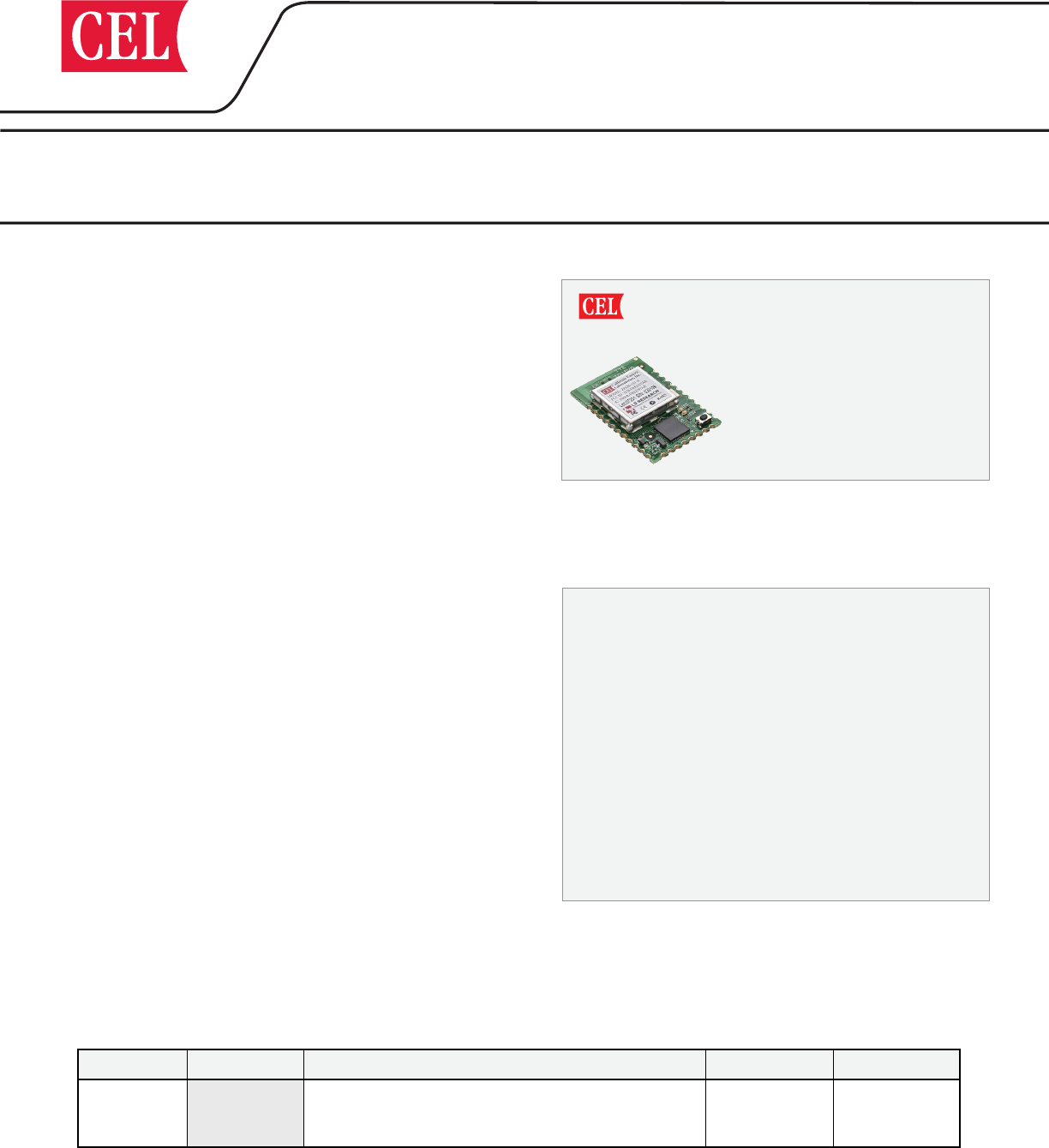
FreeStar Transceiver Module
California Eastern Laboratories (CEL)'s FreeStar Module is a
small, fully-integrated, drop-in RF transmission solution that is
ideal for ZigBee and other low cost, low power IEEE 802.15.4
RF transmission applications. FreeStar incorporates the
MC13202 transceiver IC and MC9S08GT60 microprocessor
from Freescale with a power amplier and an Inverted-F PCB
antenna. It delivers up to 4,000 feet of range and features a
streamlined communications protocol that results in the lowest
power consumption in transmit mode of any Module on the
market. The FreeStar is also FCC and CE Certied, which
eliminates the need for a costly and time-consuming approval
process when incorporated into your design.
Integrated Transceiver Module for ZigBee®/IEEE 802.15.4
The information in this document is subject to change without notice, please conrm data is current
Document No: 0001-00-07-01-000
Date Published: October 26, 2012
PRELIMINARY DATA SHEET
DESCRIPTION
ZFSM-101-3
• Communication Modes:
Point-to-Point, Point-to Multipoint, Mesh Networking
• 4,000+ feet Line of Sight Performance
• Small Form Factor:
1.4” x 1.0”
• Integrated PCB Trace Antenna
• FCC, IC and CE Certified
• RoHS Compliance
• Direct Sequence Spread Spectrum
• CSMA-CA
• Wireless Boot Loader
• Flash-Based/Upgradable
• 10 Bit A/D (2 inputs)
• General Purpose I/O (8 ports)
• Microsoft® Windows® -Based Configuration and Test Tool
• Simple Serial UART Interface
• Over 65,000 Network Addresses
FEATURES
FreeStar
ZFSM-101-3
• Transmit Power: 100 mW
• Receive Sensitivity: -91 dBm
• RF Data Rate: 250 kbps
• Based on the Freescale MC13202
transceiver IC
• 8-bit HCS08-based MCU
APPLICATIONS
Health Care
• Patient Monitoring
• Fitness Monitoring
Industrial Controls
• Asset Tracking and Monitoring
• Homeland Security
• Process Management
• Environmental Monitoring
and Control
• Heating, Ventilation,
Air-Conditioning (HVAC)
• Automated Meter Reading (AMR)
Consumer
• Human Interface Devices
(keyboard, mice, etc.)
• Remote Control
• Wireless Toys
Residential and
Commercial Automation
• Lighting Control
• Security
• Access Control
• Heating, Ventilation,
Air-Conditioning (HVAC)
• Automated Meter Reading (AMR)
Part Number Order Number Description Mins/Mults Status
FreeStar
ZFSM-101-3 ZFSM-101-3 FreeStar 100mW transceiver module PCB Trace Antenna
with / Freescale MC13202 200 pcs / 200 pcs Not Recommended
For New Designs
ORDERING INFORMATION

FreeStar ZFSM-101-3
Page 2
Introduction and Overview
Description..............................................................................................................................................................................................
1
Features
.................................................................................................................................................................................................. 1
Applications
............................................................................................................................................................................................ 1
Ordering Information.............................................................................................................................................................................
1
Module Block Diagram...........................................................................................................................................................................
3
Development Kit
..................................................................................................................................................................................... 3
System Level Function
Transceiver IC
......................................................................................................................................................................................... 3
Electrical Specication
Antenna...................................................................................................................................................................................................
4
Absolute Maximum Ratings...................................................................................................................................................................
4
Recommended Operating Conditions
................................................................................................................................................... 4
Electrical Characteristics
.......................................................................................................................................................................
5
Typical Transmit Power vs. Power Setting
.......................................................................................................................................... 5
Pin Signal & Interfaces
Pin Denitions
........................................................................................................................................................................................ 6
Connector Legend
.................................................................................................................................................................................. 7
Connector Conguration
....................................................................................................................................................................... 7
Radiation Patterns
.................................................................................................................................................................................. 8
Example Interface Diagrams
.................................................................................................................................................................. 9
Module Dimensions
................................................................................................................................................................................ 10
Module Keepouts
.................................................................................................................................................................................... 11
Processing
......................................................................................................................................................................................... 12
Shipment, Storage and Handling
............................................................................................................................................. 13
Quality
.................................................................................................................................................................................................. 13
Agency Certications
................................................................................................................................................................... 14
References and Revision History
............................................................................................................................................ 16
TABLE OF CONTENTS
FreeStar ZFSM-101-3
Page 3
The Freestar ZFSM-101-3 Module replaces the ZFSM-101-2 Module. The difference between the two modules is the
replacement of the power amplier. The design was optimized to provide similar output power between the two designs so
that there are no perceived changes by existing customers or designs. The ZFSM-101-3 can use the rmware for the ZFSM-
101-2.
The power shaping restrictions for FCC/IC and ETSI compliance are listed in the table below for reference. The power setting
restrictions must be adhered to.
TRANSCEIVER IC
Cercaon RF Channel Valid TX Power
Steps
Typical Output
Power
FCC/IC
11 thru 23 0-30 20 dBm
24 0-18 16.8 dBm
25 0-14 10.8 dBm
26 0-6 2.7 dBm
ETSI 11-26 6 2.7 dBm
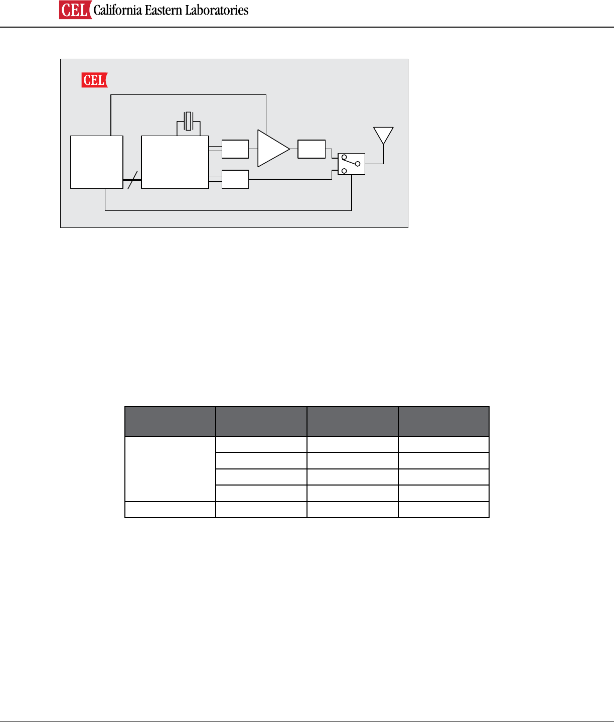
MODULE BLOCK DIAGRAM
DEVELOPMENT KIT
No Longer Available.
ANTPA Enable
16MHz
XTAL
BUS
FreeStar Module
MCU Radio
Balun
Balun
PA LPF
FreeStar ZFSM-101-3
Page 4
ABSOLUTE MAXIMUM RATINGS
Rating Value Unit
Power Supply Voltage 3.6 Vdc
RF Input Power +10 dBm
Storage Temperature Range -55 to 125 ºC
RECOMMENDED OPERATING CONDITIONS
Characteristic Min Typ Max Unit
Power Supply Voltage (Vdd) 2.1 3.3 3.6 Vdc
Input Frequency 2405 2480 MHz
Ambient Temperature Range -40 25 85 ºC
Logic Input Low Voltage 0 30% Vdd V
Logic Input High Voltage 70% Vdd Vdd V
FreeStar Modules include an integrated PCB trace antenna. The PCB antenna employs an F-Antenna topology that is com-
pact and supports an omni-directional radiation pattern. To maximize antenna efciency, an adequate ground plane must be
provided on the host PCB.
The following will signicantly contribute to antenna performance:
• The position of the module on the host board
• The position of the ground plane on the host board under the module
• Overall design of product enclosure
Poor design affects radiation patterns and can result in reection, diffraction and/or scattering of the transmitted signal.
The following are a few design guidelines to help ensure antenna performance:
• Never place the ground plane or route copper traces directly underneath the antenna portion of the module
• Never place the antenna close to metallic objects
• In the overall design, ensure that wiring and other components are not placed near the antenna
• Do not place the antenna in a metallic or metallized plastic enclosure
• Keep plastic enclosures 1cm or more from the antenna in any direction
ANTENNA
FreeStar ZFSM-101-3
Page 5
Parameter Min Typ Max Unit
General Characteristics
RF Frequency Range 2400 2483.5 MHz
Output Power (software controlled) 1 100 mW
Receiver Sensitivity @ 1% PER -91 dBm
RF Data Rate 250 kbps
Host Data Rate 19.2 kbps
Voltage Operating Range 2.1 3.6 V
General Purpose Digital I/O (8 Pins) 8Pins
RF Channels (Channels 24, 25, and 26 are set at reduced power levels) 16 Channels
DC Electrical Characteristics
Power Supply Current
(Vdd) = 3.3V, @ 25°C
Transmit Mode 100mW 170 mA
Receive Mode 50 55 mA
Standby Mode 15 uA
Output High Voltage (all digital outputs) 80% Vdd Vdd V
Output Low Voltage (all digital outputs) 0 20% Vdd V
AC Electrical Characteristics
Sensitivity for 1% packet error rate (-40 to +85ºC) – -91 dBm
Sensitivity for 1% packet error rate (25ºC) – -91 -89 dBm
Saturation (maximum input level) 10 dBm
Nominal Output Power 20 dBm
Output Power Control Range (+20 to 0 dBm) 20 dB
Error Vector Magnitude (RMS EVM) 35 %
Over the Air Data Rate 250 kbps
On-board Antenna Gain (peak) 0.8 dBi
On-board Antenna Gain (average) -3.1 dBi
TYPICAL TRANSMIT POWER VS. POWER SETTING
Power Setting Output Power
>= 30 19.8 dBm
28 19.8 dBm
26 19.8 dBm
24 19.2 dBm
22 17.6 dBm
20 17.2 dBm
18 16.8 dBm
16 16.3 dBm
14 10.8 dBm
12 10.4 dBm
10 9.8 dBm
8 9.2 dBm
6 2.7 dBm
4 2.3 dBm
2 1.9 dBm
0 1.5 dBm
ELECTRICAL CHARACTERISTICS
FreeStar ZFSM-101-3
Page 6
PIN DEFINITIONS
PIN TYPE SIGNAL
NAME ELECTRICAL DESCRIPTION
ANT2 AO/AI ANT2 INTEGRATED PBC F-ANTENNA
TPRF1 AO/AI TPRF1 COAXIAL RF TEST POINT – 50 OHMS
1GND GND GROUND
2GND GND GROUND
3GND GND GROUND
4GND GND GROUND
5DI/DO PTD3 GENERAL PURPOSE DIGITAL I/O FIRMWARE CONFIGURABLE, PORT D , BIT 3
6DI/DO PTD4 GENERAL PURPOSE DIGITAL I/O FIRMWARE CONFIGURABLE, PORT D , BIT 4
7AI PTB0 ANALOG TO DIGITAL CONVERTER INPUT, PORT B , INPUT 0
8AI PTB1 ANALOG TO DIGITAL CONVERTER INPUT, PORT B , INPUT 1
9PI VCC PRIMARY POWER INPUT: VCC = 2.4 TO 3.6 VDC
10 GND GND GROUND
11 DI MODE0 FCC / PRODUCTION TEST MODE INPUT WORD, BIT 0
12 DI MODE1 FCC / PRODUCTION TEST MODE INPUT WORD, BIT 1
13 DI MODE2 FCC / PRODUCTION TEST MODE INPUT WORD, BIT 2
14 DI/DO PTA4 GENERAL PURPOSE DIGITAL I/O FIRMWARE CONFIGURABLE PORT A, BIT 4,
KBI1P4 (KEYBOARD INTERRUPT)
15 DI/DO PTA5 GENERAL PURPOSE DIGITAL I/O FIRMWARE CONFIGURABLE PORT A, BIT 5,
KBI1P5 (KEYBOARD INTERRUPT)
16 DI/DO PTA6 GENERAL PURPOSE DIGITAL I/O FIRMWARE CONFIGURABLE PORT A, BIT 6,
KBI1P6 (KEYBOARD INTERRUPT)
17 DI PTA7 DIGITAL INPUT CONFIGURED TO INTERRUPT ON RISING EDGE OF SIGNAL TO WAKE
UP MODULE FROM SLEEP MODE. PORT A, BIT 7, KBI1P7 (KEYBOARD INTERRUPT)
18 DI/DO PTGO PORT G, BIT 0, BKGD/MS (BACKGROUND/MODE SELECT, FOR PROGRAMMING
AND FIRMWARE DEBUG)
19 DI/DO /RESET1MASTER RESET, ACTIVE LOW
20 DI/DO PTC0 GENERAL PURPOSE DIGITAL I/O FIRMWARE CONFIGURABLE PORT C, BIT 0,
SCI2 TXD2 (SERIAL COMMUNICATION INTERFACE 2, TRANSMIT DATA)
21 DI/DO PTC1 GENERAL PURPOSE DIGITAL I/O FIRMWARE CONFIGURABLE PORT C, BIT 1,
SCI2 RXD2 (SERIAL COMMUNICATION INTERFACE 2, RECEIVE DATA)
22 DI/DO PTC5 RESERVED
23 DO TXD APPLICATION TRANSMIT DATA OUTPUT (SCI1, TXD1)
24 DI RXD APPLICATION RECEIVE DATA INPUT (SCI1, RXD1)
25 GND GND GROUND
26 GND GND GROUND
27 GND GND GROUND
28 GND GND GROUND
29 GND GND GROUND
30 GND GND GROUND
Note: 1 Use an Open Collector Output to Drive the Reset pin or put a 1k Ohm resistor in series with the driving source.
Normally the reset pin is an output; however, under brown out and other reset conditions the Freescale
microcontroller will drive the pin low.
FreeStar ZFSM-101-3
Page 7
CONNECTOR LEGEND
TYPE DEFINITION
DI DIGITAL INPUT
DO DIGITAL OUTPUT
AI ANALOG INPUT
AO ANALOG OUTPUT
PI POWER INPUT
GND GROUND
LOGIC INPUT HIGH 0.7 (VCC) < VIH < (VCC)
LOGIC INPUT LOW 0 < VIL < 0.3 (VCC)
LOGIC OUTPUT HIGH (VCC – 0.8) < VOH < VCC
LOGIC OUTPUT LOW 0 < VOL < 0.2 (VCC)
CONNECTOR CONFIGURATION
GND
SHD1
GND
GND
GND
GND
GND
RXD
TXD
PTC5
PTC1
PTC0
GND
GND
GND
GND
PDT3
PDT4
PDB0
PDB1
VCC
GND
MODE0
MODE1
MODE2
PTA4
PTA5
PTA6
PTA7
PTG0
/RESET
Note: The PIN Numbering begins at top left-hand side with pin number 1 and follows counter-clockwise
about the perimeter of the module.

FreeStar ZFSM-101-3
Page 8
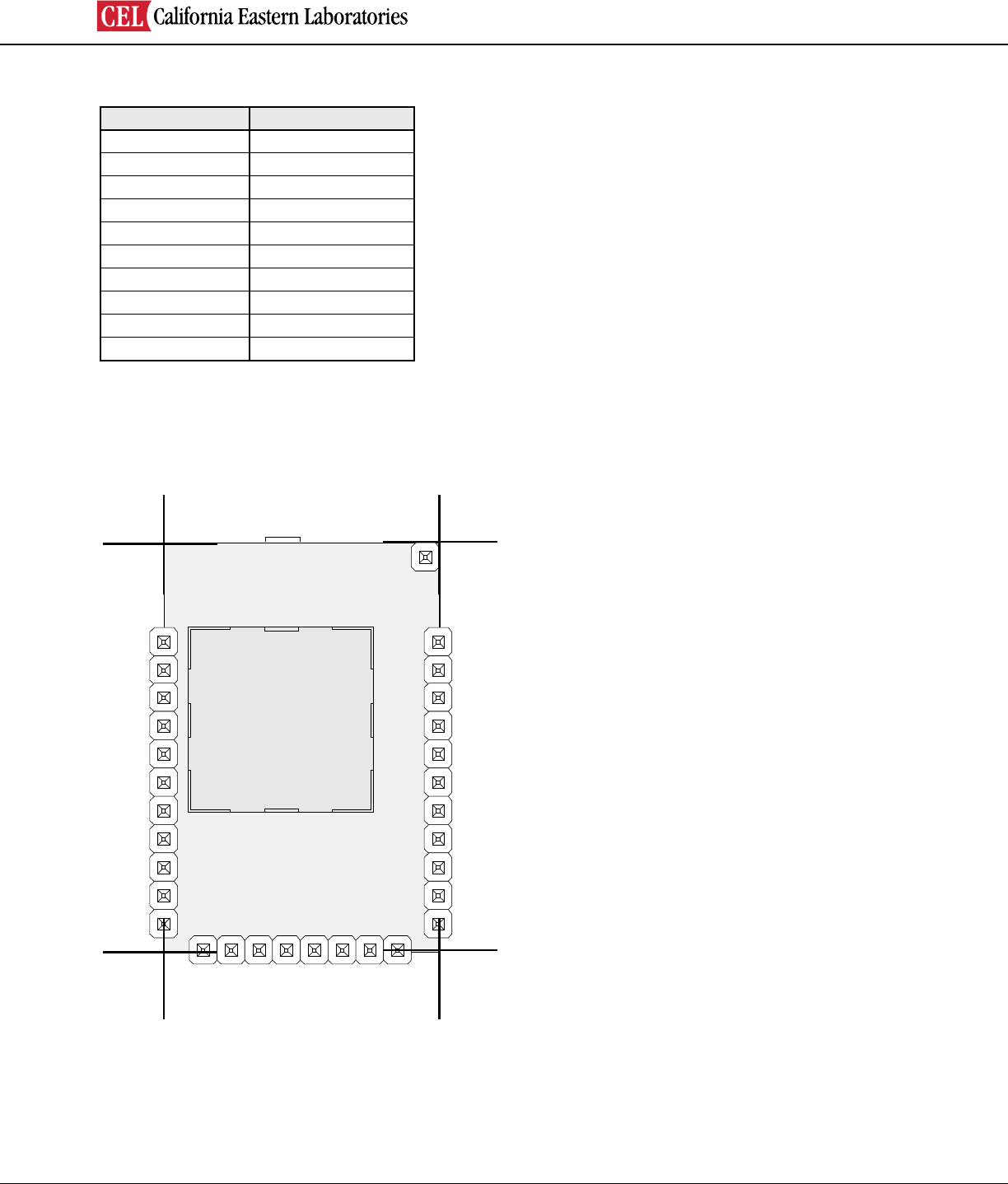
FreeStar Rev B 2440 MHz
Device Orientation Polarization Gain (dB)
Max Avg
(V) Vertical 0.60 -1.72
(V) Horizontal -7.27 -12.37
(H) Vertical -4.00 -10.91
(H) Horizontal 0.02 -5.90
(F) Vertical -6.62 -13.52
(F) Horizontal 0.85 -4.67
Total Average Gain (dB) -3.15
Vertical
Horizontal
Flat
RADIATION PATTERNS
FreeStar ZFSM-101-3
Page 9
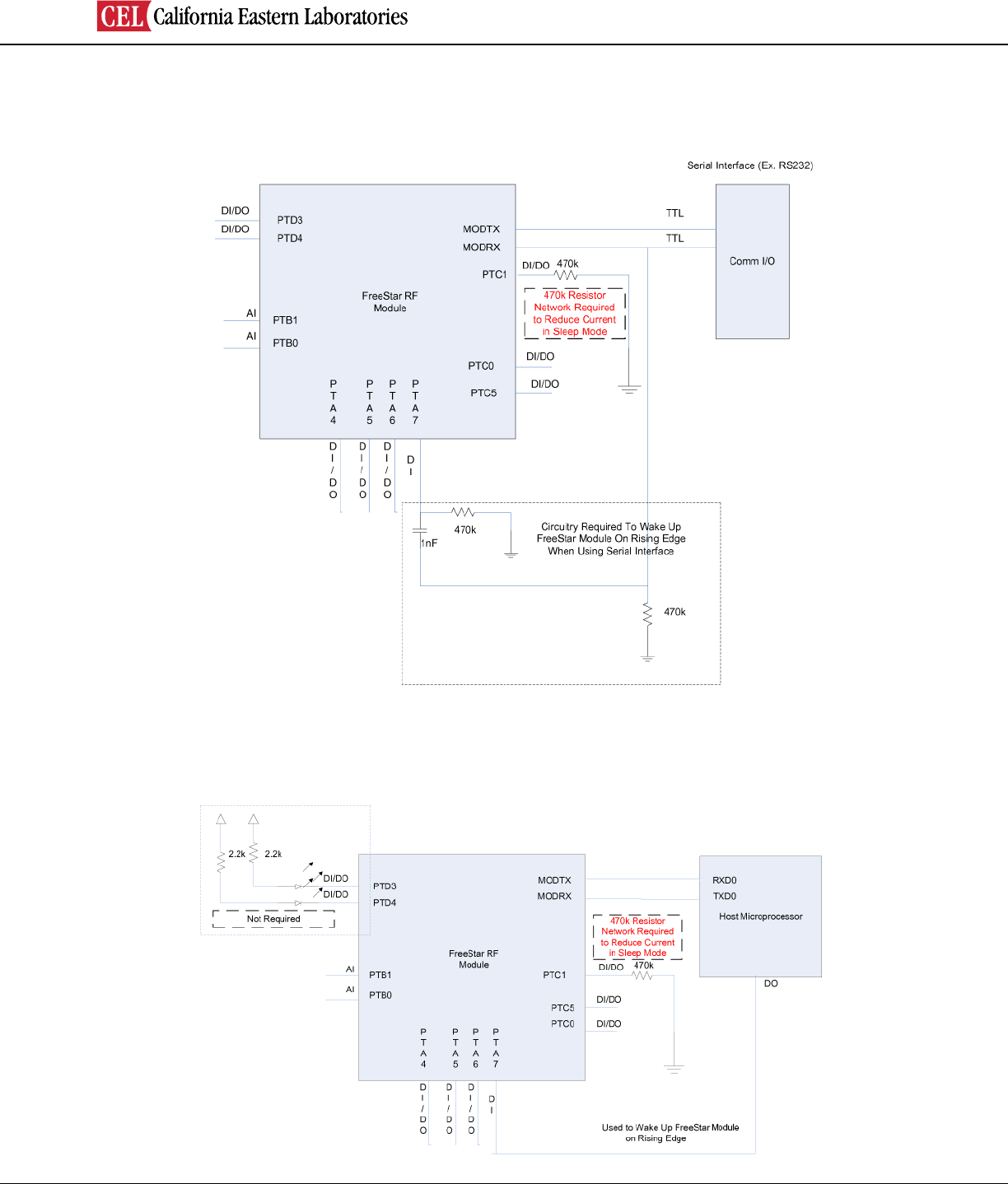
EXAMPLE INTERFACE DIAGRAMS
Sample Connection Diagram when Using Serial Interface
Sample Connection Diagram when Using Host Processor Interface
FreeStar ZFSM-101-3
Page 10
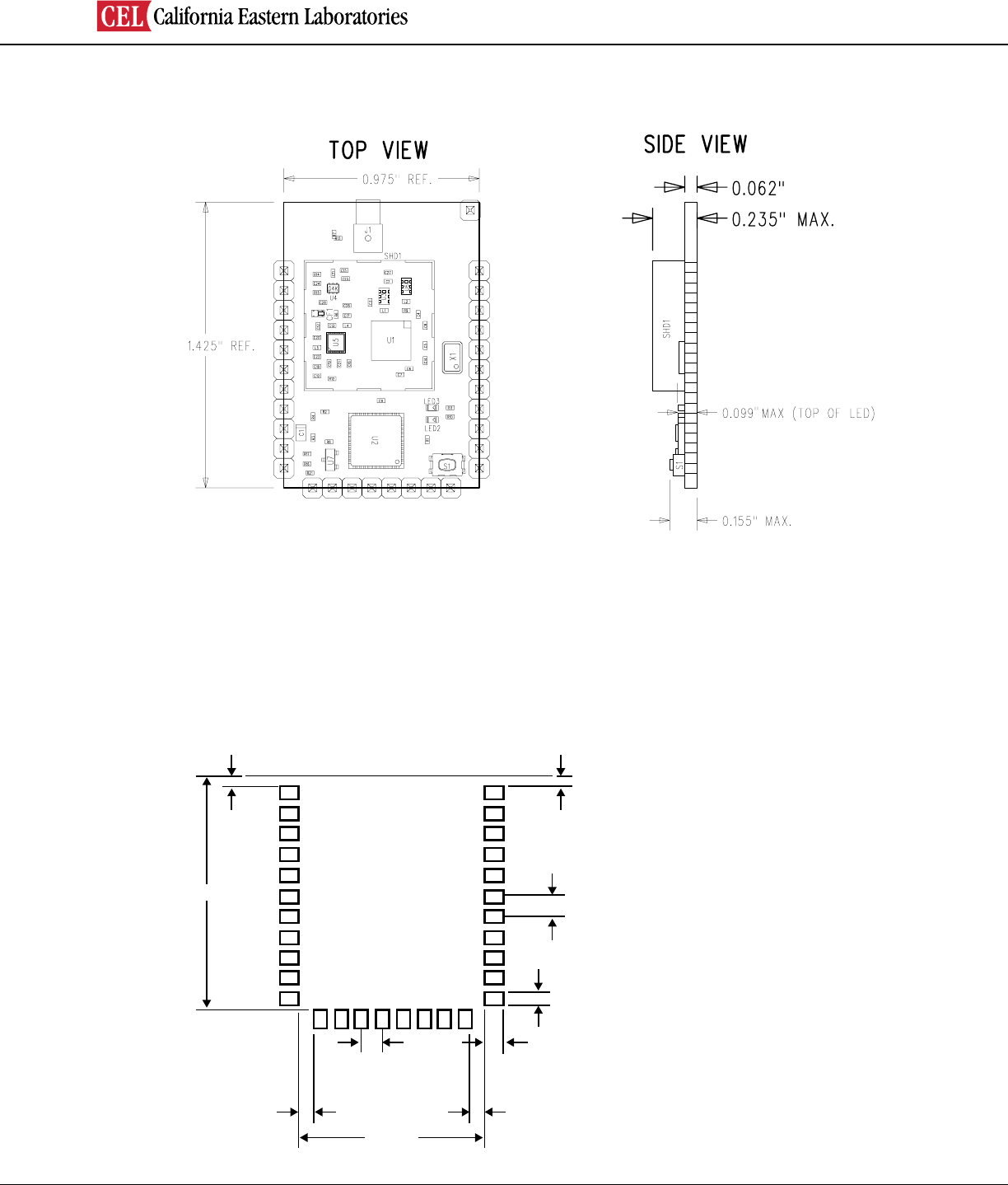
MODULE DIMENSIONS
Note: Unless otherwise specied, dimensions are in inches.
1
1.115”
0.098”
0.060”
0.090”
0.098”
0.068”
0.885”
0.068”
(2.5mm) Pitch Throughout
Recommended Host PCB Board Edge
PCB COPPER PATTERN
FOR REFERENCE ONLY
TOP VIEW
(2.5mm)
Pitch Throughout
TYP 30 Places
TYP 30 Places
0.047”
0.047”
30
PCB FOOTPRINT
Note: Unless otherwise specied, dimensions are in inches.
FreeStar ZFSM-101-3
Page 11
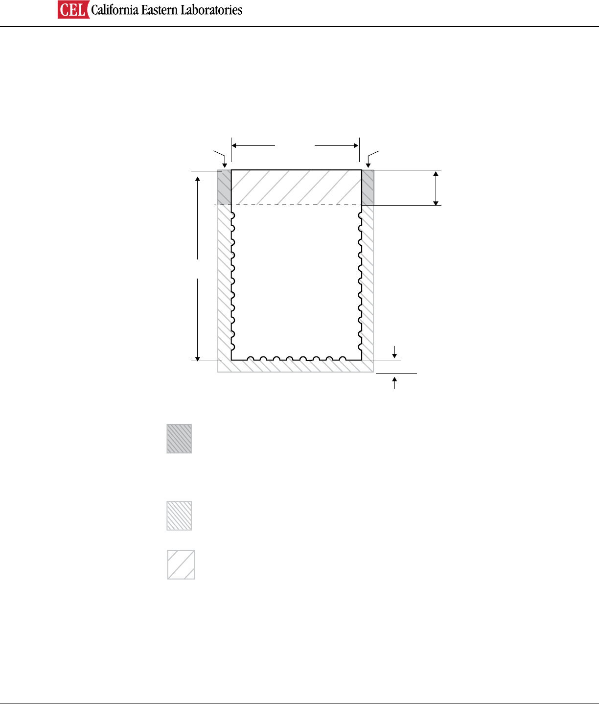
MODULE KEEPOUTS
Note: Unless otherwise specied, dimensions are in inches.
COMPONENT KEEPOUT
COPPER AND COMPONENT KEEPOUT
1.425”
0.265”
RECOMMENDED MODULE
EXTENSION OVER EDGE
OF HOST PCB
COMPONENT KEEPOUT - NO HOST BOARD PERIPHERAL COMPONENTS
ALLOWED WITHIN 0.100” OF MODULE
IF OVER HANG METHOD OF MOUNTING IS NOT USED
• NO COMPONENTS ON EITHER TOP OR BOTTOM SIDES
OF HOST PCB ALLOWED IN THIS AREA
• NO COPPER/TRACES ALLOWED ON ANY LAYER
OF HOST PCB IN THIS AREA
Module - Dimensions and Keepouts
TOP VIEW
0.100” PRIMETER AROUND MODULE
0.975”
COPPER AND COMPONENT KEEPOUT AREA
• NO COPPER/TRACES ALLOWED ON ANY LAYER
OF HOST PCB IN THIS AREA
• NO COMPONENTS ON EITHER TOP OR BOTTOM SIDES
OF HOST PCB ALLOWED WITHIN 0.100” OF MODULE
COPPER AND COMPONENT KEEPOUT
MODULE
TOP VIEW
HOST PCB EDGE
1
2
3
4
5
6
7
8
9
10
11
30
29
28
27
26
25
24
23
22
21
20
12 13 14 15 16 17 18 19
COPPER KEEPOUT
FreeStar ZFSM-101-3
Page 12
PROCESSING
Recommended Reow Prole
Parameters Values
Ramp Up Rate (from Tsoakmax to Tpeak) 3º/sec max
Minimum Soak Temperature 150ºC
Maximum Soak Temperature 200ºC
Soak Time 60-120 sec
TLiquidus 217ºC
Time above TL 60-150 sec
Tpeak 250ºC
Time within 5º of Tpeak 20-30 sec
Time from 25º to Tpeak 8 min max
Ramp Down Rate 6ºC/sec max
Pb-Free Solder Paste
Use of “No Clean” solder paste is strongly recommended, as it does not require cleaning after the soldering process.
Note: The quality of solder joints on the castellations (‘half vias’) where they contact the host board should meet the appropriate IPC
Specication. See the latest IPC-A-610 Acceptability of Electronic Assemblies, Castellated Terminations section.
Cleaning
In general, cleaning the populated modules is strongly discouraged. Residuals under the module cannot be easily removed
with any cleaning process.
• Cleaning with water can lead to capillary effects where water is absorbed into the gap between the host board and
the module. The combination of soldering ux residuals and encapsulated water could lead to short circuits between
neighboring pads. Water could also damage any stickers or labels.
• Cleaning with alcohol or a similar organic solvent will likely ood soldering ux residuals into the two housings, which
is not accessible for post-washing inspection. The solvent could also damage any stickers or labels.
• Ultrasonic cleaning could damage the module permanently.
The best approach is to consider using a “No Clean” solder paste and eliminate the post-soldering cleaning step.
Optical Inspection
After soldering the module to the host board, consider optical inspection to check the following:
• Proper alignment and centering of the module over the pads.
• Proper solder joints on all pads.
• Excessive solder or contacts to neighboring pads or vias.
Repeating Reow Soldering
Only a single reow soldering process is encouraged for host boards.
Wave Soldering
If a wave soldering process is required on the host boards due to the presence of thru hole components, only a single wave
soldering process is encouraged.

FreeStar ZFSM-101-3
Page 13
PROCESSING (Continued)
Hand Soldering
Hand soldering is possible. When using a soldering iron, follow IPC recommendations (reference document IPC-7711).
Rework
The module can be unsoldered from the host board. Use of a hot air rework tool should be programmable and the solder
joint and module should not exceed the maximum peak reow temperature of 250 ºC.
Caution
If temperature ramps exceed the reow temperature prole, module and component damage may occur due to thermal
shock. Avoid overheating.
Warning
Never attempt a rework on the module itself, (e.g., replacing individual components). Such actions will terminate
warranty coverage.
Additional Grounding
Attempts to improve module or system grounding by soldering braids, wires or cables onto the module RF shield cover is
done at the customer's own risk. The numerous ground pins at the module perimeter should be sufcient for optimum
immunity to external RF interference.
QUALITY
CEL modules offer the highest quality at competitive prices. Our modules are manufactured in compliance with the IPC-A-610
specication, Class II. Our modules go through JESD22 qualication processes which includes high temperature operating life
tests, mechanical shock, temperature cycling, humidity and reow testing. CEL modules are 100% factory tested for RF and
DC performance. In addition, every production lot is sample tested for compliance with CEL’s high quality and performance
standards.
CEL builds quality into our products giving our customers the condence when integrating our products into their systems.
SHIPMENT, HANDLING AND STORAGE
Shipment
The modules are delivered in trays of 50.
Handling
The modules are designed and packaged to be processed in an automated assembly line.
Warning
The modules contain highly sensitive electronic circuitry. Handling without proper ESD protection may destroy or damage
the module permanently.
Warning
The modules are moisture-sensitive devices. Appropriate handling instructions and precautions are summarized in J-STD-033.
Read carefully to prevent permanent damage due to moisture intake.
Moisture Sensitivity Level (MSL)
MSL 3, per J-STD-033.
Storage
Storage/shelf life in sealed bags is 12 months at <40°C and <90% relative humidity.

FreeStar ZFSM-101-3
Page 14
AGENCY CERTIFICATIONS
FCC Compliance Statement (Part 15.19) Section 7.15 of RSS-GEN
This device complies with Part 15 of the FCC Rules. Operation is subject to the following two conditions:
1. This device may not cause harmful interference
2. This device must accept any interference received, including interference that may cause undesired operation
Le présent appareil est conforme aux CNR d'Industrie Canada applicables aux appareils radio exempts de licence.
L'exploitation est autorisée aux deux conditions suivantes:
1. l'appareil ne doit pas produire de brouillage, et
2. l'utilisateur de l'appareil doit accepter tout brouillage radioélectrique subi, même si le brouillage est susceptible
d'en compromettre le fonctionnement
Warning (Part 15.21)
Changes or modications not expressly approved by CEL could void the user's authority to operate the equipment.
20 cm Separation Distance
To comply with FCC/IC RF exposure limits for general population/uncontrolled exposure, the antenna(s) used for this trans-
mitter must be installed to provide a separation distance of at least 20 cm from all persons and must not be co-located or
operating in conjunction with any other antenna or transmitter.
OEM Responsibility to the FCC Rules and Regulations
The FreeStar Module has been certied per FCC Part 15 rules for integration into products without further testing or certi-
cation. To fulll the FCC certication requirements, the OEM of the FreeStar Module must ensure that the
information provided on the FreeStar Label is placed on the outside of the nal product. The FreeStar Module is labeled
with its own FCC ID Number. If the FCC ID is not visible when the module is installed inside another device, then the out-
side of the device into which the module is installed must also display a label referring to the enclosed module. This exterior
label can use wording such as the following: “Contains Transmitter Module FCC ID: TFB-FREESTAR3” or “Contains FCC ID:
TFB-FREESTAR3”
The OEM of the FreeStar Module must only use the approved antenna, that has been certied with this module. The OEM
of the FreeStar Module must test their nal product conguration to comply with Unintentional Radiator Limits before declaring
FCC compliance per Part 15 of the FCC rules.
IC Certication — Industry Canada Statement
The term "IC" before the Certication/Registration number only signies that the Industry Canada technical specications
were met.
This device complies with Industry Canada license-exempt RSS standard(s). Operation is subject to the following two con-
ditions: (1) this device may not cause interference, and (2) this device must accept any interference, including interference
that may cause undesired operation of the device.
Certication IC - Déclaration d'Industrie Canada
Le terme "IC" devant le numéro de certication/d'enregistrement signie seulement que les spécications techniques
Industrie Canada ont été respectées.-
Le présent appareil est conforme aux CNR d'Industrie Canada applicables aux appareils radio exempts de licence.
L'exploitation est autorisée aux deux conditions suivantes : (1) l'appareil ne doit pas produire de brouillage, et (2) l'utilisateur
de l'appareil doit accepter tout brouillage radioélectrique subi, même si le brouillage est susceptible d'en compromettre le
fonctionnement
FreeStar ZFSM-101-3
Page 15
AGENCY CERTIFICATIONS (Continued)
Section 14 of RSS-210
The installer of this radio equipment must ensure that the antenna is located or pointed such that it does not emit RF eld in
excess of Health Canada limits for the general population. Consult Safety Code 6, obtainable from Health Canada's
website: http://www.hc-sc.gc.ca/ewh-semt/pubs/radiation/99ehd-dhm237/index-eng.php
L'article 14 du CNR-210
Le programme d'installation de cet équipement radio doit s'assurer que l'antenne est située ou orientée de telle sorte qu'il
ne pas émettre de champ RF au-delà des limites de Santé Canada pour la population générale. Consulter le Code de
sécurité 6, disponible sur le site Web de Santé Canada: http://www.hc-sc.gc.ca/ewh-semt/pubs/radiation/99ehd-dhm237/
index-eng.php
EMC Certication
FCC Part 15.247 Module Certied (Portable)
EN 300 328 1 Certied / CE Approved
The FreeStar Module has been tested and certied for the European Union.
OEM Responsibility to the European Union Compliance Rules
If the FreeStar Module is to be incorporated into a product, the OEM must verify compliance of the nal product to the Eu-
ropean Harmonized EMC and Low-Voltage/Safety Standards. A Declaration of Conformity must be issued for each of these
standards and kept on le as described in Annex II of the R&TTE Directive.
The manufacturer must maintain the user's guide and adhere to the settings described in the manual for maintaining
European Union Compliance. If any of the specications are exceeded in the nal product, the OEM is required to
make a submission to the notied body for compliance testing.
OEM Labeling Requirements
The `CE' mark must be placed on the OEM product in a visible location. The CE mark shall consist of the initials “CE” with
the following form:
• If the CE marking is reduced or enlarged, the proportions given in the above graduated
drawing must be adhered to
• The CE mark must be a minimum of 5mm in height
• If the use of the module is subject to restrictions in the end application, the CE marking on the
OEM product should also include the alert sign as shown in the picture to the right
Australia Certication
Number: AS/NZS 4268
FreeStar ZFSM-101-3
Page 16
REFERENCES & REVISION HISTORY
Previous Versions Changes to Current Version Page(s)
0001-00-07-01-000
(Issue ES) October 10, 2011 Initial preliminary datasheet. N/A
0001-00-07-01-000
(Issue ES) October 26, 2011 Updated electrical characteristics, software revisions. 1, 4, 6
0001-00-07-01-000
October 18, 2012 Rolled part number to -3, updated power amplier section 1, 2, 3, 5
0001-00-07-01-000
October 26, 2012 Updated FCC information 3
Disclaimer
• The information in this document is current as of the published date. The information is subject to change without
notice. For actual design-in, refer to the latest publications of CEL data sheets or data books, etc., for the most
up-to-date specications of CEL products. Not all products and/or types are available in every country. Please
check with an CEL sales representative for availability and additional information.
• No part of this document may be copied or reproduced in any form or by any means without the prior written
consent of CEL. CEL assumes no responsibility for any errors that may appear in this document.
• CEL does not assume any liability for infringement of patents, copyrights or other intellectual property rights of
third parties by or arising from the use of CEL products listed in this document or any other liability arising from the
use of such products. No license, express, implied or otherwise, is granted under any patents, copyrights or other
intellectual property rights of CEL or others.
• Descriptions of circuits, software and other related information in this document are provided for illustrative
purposes in semiconductor product operation and application examples. The incorporation of these circuits,
software and information in the design of a customer’s equipment shall be done under the full responsibility of the
customer. CEL assumes no responsibility for any losses incurred by customers or third parties arising from the use
of these circuits, software and information.
• While CEL endeavors to enhance the quality, reliability and safety of CEL products, customers agree and
acknowledge that the possibility of defects thereof cannot be eliminated entirely. To minimize risks of damage to
property or injury (including death) to persons arising from defects in CEL products, customers must incorporate
sufcient safety measures in their design, such as redundancy, re-containment and anti-failure features.