Landis Gyr ZIG527602 5276 Zigbee Transceiver Module User Manual RDD212 01

Landis + Gyr, Inc. 5276 Zigbee Transceiver Module RDD212 01
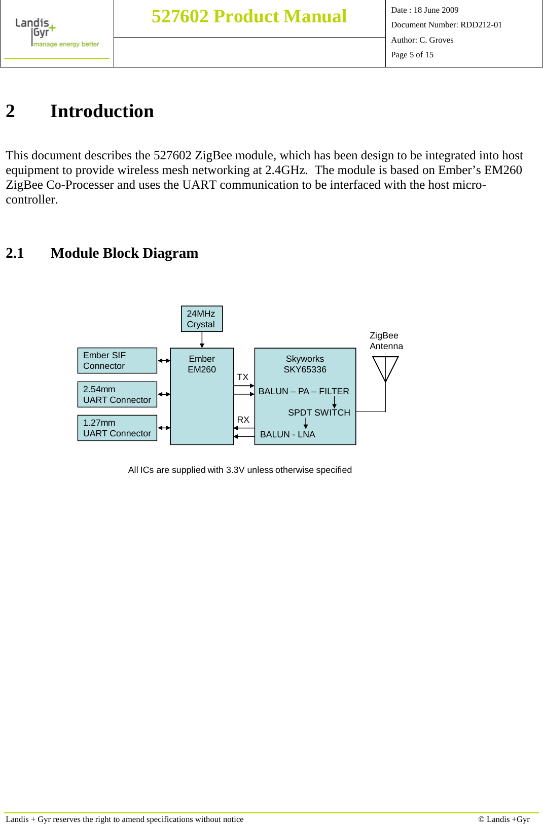
Manual

        Product Manual 527602  Document Number: RDD212-01 Date : 18 June 2009 Document Number: RDD212-01 Author: C. Groves Approved by: G.Lane INT314-04 © Landis + Gyr
 527602 Product Manual  Date : 18 June 2009 Document Number: RDD212-01 Author: C. Groves Page 2 of 15    Landis + Gyr reserves the right to amend specifications without notice  © Landis +Gyr Revision History  Index Date  Name  Comments 1  18.6.2009  C. Groves  Initial Release                                                                                                      Subject to change without notice.     Landis + Gyr 1 Lysander Drive, Northfields Industrial Estate, Market Deeping, Peterborough PE6 8FB
 527602 Product Manual  Date : 18 June 2009 Document Number: RDD212-01 Author: C. Groves Page 3 of 15    Landis + Gyr reserves the right to amend specifications without notice  © Landis +Gyr Table of Contents 1ABBREVIATIONS .......................................................................................................................................................... 42INTRODUCTION ............................................................................................................................................................ 52.1MODULE BLOCK DIAGRAM ............................................................................................................................................ 53PRODUCT APPROVALS .............................................................................................................................................. 63.1FCC APPROVALS ........................................................................................................................................................... 63.2EUROPEAN APPROVALS ................................................................................................................................................. 73.3MAXIMUM ALLOWABLE POWER LEVELS ....................................................................................................................... 74HARDWARE DESCRIPTION ....................................................................................................................................... 84.1EM260 ........................................................................................................................................................................... 84.2SKY65336 ..................................................................................................................................................................... 84.3CRYSTAL ........................................................................................................................................................................ 84.4RF SHIELD ..................................................................................................................................................................... 84.5ANTENNA ....................................................................................................................................................................... 84.6TEST POINTS .................................................................................................................................................................. 85MECHANICAL DRAWING .......................................................................................................................................... 96CONNECTIONS ............................................................................................................................................................ 106.1.1UART Connector (J2 and J4) ............................................................................................................................ 106.1.2M Bus Connector (J1) ........................................................................................................................................ 106.1.3Ember SIF Connector (J3) ................................................................................................................................. 116.2UART CONNECTOR DETAILED DESCRIPTION .............................................................................................................. 126.2.1Overview ............................................................................................................................................................ 126.2.2P2_TX and P2_RX ............................................................................................................................................. 126.2.3P2_CTS and P2_RTS ......................................................................................................................................... 126.2.4FORCE_BOOT .................................................................................................................................................. 136.2.5SYSRST .............................................................................................................................................................. 136.2.6P2_AUX1 ........................................................................................................................................................... 136.2.7OPTION_CARD_ID .......................................................................................................................................... 137ELECTRICAL SPECIFICATION ............................................................................................................................... 147.1ABSOLUTE MAXIMUM RATINGS .................................................................................................................................. 147.2RECOMMENDED OPERATING CONDITIONS ................................................................................................................... 147.3ELECTRICAL SPECIFICATION ........................................................................................................................................ 15
 527602 Product Manual  Date : 18 June 2009 Document Number: RDD212-01 Author: C. Groves Page 4 of 15   Landis + Gyr reserves the right to amend specifications without notice  © Landis +Gyr 1 Abbreviations  BPF    Band Pass Filter CFR    Code of Federal Regulations FCC   Federal Communications Commission LNA    Low Noise Amplifier LPF    Low Pass Filter OTA    Over the Air PA   Power Amplifier RF   Radio Frequency RX   Receive SPDT    Single Pole Double Throw TBC    To Be Confirmed TX   Transmit UL   Underwriters Laboratories
 527602 Product Manual  Date : 18 June 2009 Document Number: RDD212-01 Author: C. Groves Page 5 of 15   Landis + Gyr reserves the right to amend specifications without notice  © Landis +Gyr 1.27mmUART ConnectorZigBeeAntennaAll ICs are supplied with 3.3V unless otherwise specified Ember SIF Connector2.54mmUART Connector24MHzCrystalEmberEM260 SkyworksSKY65336BALUN – PA – FILTER SPDT SWITCHBALUN - LNATXRX2 Introduction  This document describes the 527602 ZigBee module, which has been design to be integrated into host equipment to provide wireless mesh networking at 2.4GHz.  The module is based on Ember’s EM260 ZigBee Co-Processer and uses the UART communication to be interfaced with the host micro-controller.  2.1 Module Block Diagram
 527602 Product Manual  Date : 18 June 2009 Document Number: RDD212-01 Author: C. Groves Page 6 of 15   Landis + Gyr reserves the right to amend specifications without notice  © Landis +Gyr 3 Product Approvals 3.1 FCC Approvals The 5276 ZigBee Module conforms to FCC CFR 47 part 15.   This device complies with Part 15 of the FCC rules.  Operation is subject to the following two conditions: (1) this device may not cause harmful interference, and (2) this device must accept any interference received, including interference that may cause undesired operation.         FCC ID : ROV-ZIG527602   When the 5276 ZigBee Module is integrated inside another device then the outside of this device must also display a label referring to the enclosed module.  This exterior label can use wording such as “Contains Transmitter Module FCC ID : ROV-ZIG527602” or “Contains FCC ID : ROV-ZIG527602”  This module complies with the USA SAR requirements and is not intended to be operated within 20cm of the body.  The following statement must be included as a CAUTION statement in manuals for OEM product to alert users on FCC RF exposure compliance:  “WARNING: To satisfy FCC RF exposure requirement for mobile transmitting device, a separation distance of 20cm or more should be maintain between the antenna of this device and the persons during operation.  To ensure compliance, operations at closer distances than this are not recommended.”  Any modification or changes to this module may invalidate the certification and the user’s authority to operate the equipment in the USA.
 527602 Product Manual  Date : 18 June 2009 Document Number: RDD212-01 Author: C. Groves Page 7 of 15   Landis + Gyr reserves the right to amend specifications without notice  © Landis +Gyr 3.2 European Approvals The module has been designed to meet the following European approvals:   Electromagnetic Compatibility Radio Spectrum Matters; Short Range Devices; Radio Equipment to be used in the 25 MHz to 1,000 MHz Frequency Range with Power Levels Ranging up to 500mW; Part 1: Technical Characteristics and Test Methods EN 300 328  V1.7.1 Electromagnetic compatibility and Radio spectrum Matters (ERM); Electromagnetic Compatibility (EMC) standard for radio equipment and services; Part 17: Specific conditions for 2,4 GHz wideband transmission systems and 5GHz high performance RLAN equipment. EN 301 489-17  V1.2.1 Information technology equipment. Safety. General requirements IEC 60950-1:2001 (including amendment 11:2004)   3.3 Maximum Allowable Power Levels The maximum allowable power levels are restricted by the relevant regulatory body for target country of deployment.  In order to comply with these appropriate approvals the EM260 and Skyworks devices must be configured in software to transmit within these limits. The following table shows the MAXIMUM allowable transmission levels allow according to the relevant approval body.  These levels must be set by the OEM equipment.  Approval Body  EM260  Channel 26 Power Level EM260 Channel 25 Power Level  EM260 All Other Channels Power Level Skyworks Power Level Mode FCC  -20 dBm  -3 dBm  +3 dBm  HIGH R&TTE  0 dBm  0 dBm  0 dBm  LOW  Please check with the design team for the latest information.
 527602 Product Manual  Date : 18 June 2009 Document Number: RDD212-01 Author: C. Groves Page 8 of 15   Landis + Gyr reserves the right to amend specifications without notice  © Landis +Gyr 4 Hardware Description The 5276 ZigBee Module contains the EM260 from Ember, a 24MHz crystal reference and the SKY65336 Front End Module (FEM) from Skyworks.  It has an integrated printed inverted F antenna matched to the FEM for optimum performance. 4.1 EM260 The Ember EM260 Co-Processor solution provides a wireless ZigBee mesh networking capabilities with other ZigBee enabled devices.  The EM260 is a 2.4GHz IEEE 802.15.4 compliant radio transceiver with a 16-bit microprocessor.  IEEE802.15.4 uses Offset Quadrature Phase Shift Keying (O-QPSK) Modulation Scheme.  The EM260 comes in a 6mm x 6mm, 40 pin QFN package.  Further information on the EM260 device, including how to correctly interface with the host device can be found at www.ember.com. 4.2 SKY65336 The Skyworks front end module, SKY65336, will be used to provide a PA and LNA gain stage with fully integrated impedance matching and filtering.   This FEM comes in an 8mm x 8mm 28 pin MCM package.   4.3 Crystal There is a highly accurate 24MHz crystal fitted to the PCB.  This is because the initial tolerance, temperature stability and ageing directly correspond to life that a transceiver pair can communicate.  The crystal used in this design will have a maximum tolerance of ±40ppm, including initial, ageing (5 year prediction) and temperature tolerance.  Calibration of the crystal would further improve the lifetime of the communication system. 4.4 RF Shield There is an RF shield fitted to the module. 4.5 Antenna The antenna is an integrated printed ¼ wave inverted F antenna.  This has a theoretical maximum peak gain of 5.15dBi. 4.6 Test Points Due to the compact nature of the design and to maintain optimal RF performance no test points have been added to the main circuitry on the ZigBee module.   For programming debug and bootloading the J2 and J3 connectors should be used.  For Production RF testing, TP11 should e used to measure the conducted RF output.  For RF Development and antenna matching TP12 may be used.  If TP12 is used R19 should be a zero ohm link.  In all other instances, including production, R19 must not be fitted.
 527602 Product Manual  Date : 18 June 2009 Document Number: RDD212-01 Author: C. Groves Page 9 of 15   Landis + Gyr reserves the right to amend specifications without notice  © Landis +Gyr 5 Mechanical Drawing                       Top View  Notes:  J3 may be accessed from both sides of the PCB, however to avoid a crossover connector, i.e. direct connection, to Ember development or production equipment it should be accessed from layer 4 (bottom or no component side).  Otherwise a crossover connector will be required.
 527602 Product Manual  Date : 18 June 2009 Document Number: RDD212-01 Author: C. Groves Page 10 of 15   Landis + Gyr reserves the right to amend specifications without notice  © Landis +Gyr 6 Connections 6.1.1  UART Connector (J2 and J4) Note J2 and J4 are duplicate connectors Connector    10 way connector Format         2 x 5 way double row Pitch     2.54mm or 1.27mm Suggested Connector   Samtec        TSW-105-25-L-D-RA or TSM-105-04-x-DV-M  Name  Pin  Description +3V3  1  Supply for circuitry P2_TX_SCL 2 UART Data TX P2_RX_SDA 3 UART Data RX P2_Aux1  4  Power Mode – high or Low Power P2_CTS  5  UART Flow control CTS SYSRST  6  Reset (Active Low) P2_RTS  7  UART Flow control RTS FORCE_BOOT 8 Force Bootloader (Hold Low during Reset) OPTION_CARD_ID 9  Analogue voltage to identify card type 0V 10 Ground  6.1.2  M Bus Connector (J1) Connector    4 way connector Format         2 x 2 way double row Pitch     2.54mm Suggested Connector   Not Required  Name  Pin  Description NC 1,2, 3,4 No Connection
 527602 Product Manual  Date : 18 June 2009 Document Number: RDD212-01 Author: C. Groves Page 11 of 15   Landis + Gyr reserves the right to amend specifications without notice  © Landis +Gyr 6.1.3 Ember SIF Connector (J3) Connector    10 way connector Format         5 x 2 way double row Pitch     0.05 inch Suggested Connector   Samtec       FTSH-105-01-F-DV-K (connected to layer 4 of PCB)   Name  Pin  Description VBRD  1  Supply for circuitry (+3V3 recommended) SIF_MISO 2 Serial Interface (Master Input, Slave Output) SBDG 3 Debug Signal SIF_MOSI 4 Serial Interface (Master Output, Slave Input) GND 5 Ground SIF_CLK  6  Serial Interface (Clock) nSIF_LOAD  7  Serial Interface (Load Strobe) nRESET  8  EM260 Reset (Active Low) PTI_EN  9  Packet Trace Frame Signal PTI_DATA  10  Packet Trace Data Signal (500kbps)
 527602 Product Manual  Date : 18 June 2009 Document Number: RDD212-01 Author: C. Groves Page 12 of 15   Landis + Gyr reserves the right to amend specifications without notice  © Landis +Gyr 6.2 UART Connector Detailed Description 6.2.1 Overview This section provides a detailed description of the connections between the ZigBee module and the host MCU.  Name  Host Micro Function  EM260 Function  EM260 Pin # P2_TX  UART Transmitted Data  UART Received Data  26 P2_RX  UART Received Data  UART Transmitted Data  25 P2_CTS  UART CTS  UART RTS  16 P2_RTS  UART RTS  UART CTS  15 SYSRST  EM260 RESET  EM260 RESET  11 FORCE_BOOT  Force EM260 Bootloader  Force EM260 Bootloader  23  6.2.2 P2_TX and P2_RX Transmitted and received serial data between the host micro and the ZigBee module.  The signal lines are connected directly to the EM260.  P2_TX   Transmitted data on host MCU.       Received data on the EM260 (pin 26). P2_RX   Received data on host MCU.       Transmitted data on the EM260 (pin 25).  6.2.3 P2_CTS and P2_RTS  The UART hardware flow control lines between the host micro and the ZigBee module. The signal lines have been connected directly to the EM260.  P2_CTS  Clear To Send on the host MCU.     Ready To Send on the EM260 (pin 16). P2_RTS  Ready To Send on host MCU.       Clear To Send on EM260 (Pin 15).
 527602 Product Manual  Date : 18 June 2009 Document Number: RDD212-01 Author: C. Groves Page 13 of 15   Landis + Gyr reserves the right to amend specifications without notice  © Landis +Gyr 6.2.4 FORCE_BOOT This line can force the EM260 into bootloader mode should the software bootloader command fail.  This gives the host micro a fail safe recovery method for bootloading the EM260.  Consideration should be given to bootloading recovery method should the over the air system fail, for example if the EM260 is corrupted.  Bootloader can be activated by pulling FORCE_BOOT low during a RESET.   This line is connected to PTI_DATA on the EM260 (Pin 23) via a 330 Ohm limiting resistor.  It has been connected to PB12 (pin 51) on the host micro.  Please refer to EM260 documetation for correct implementation of hardware bootloader. 6.2.5 SYSRST This line will force the EM260 into reset (active low).  It is connected to nRESET line of the EM260 (pin 11) and PE10 (pin 41) on the host micro. 6.2.6 P2_AUX1 This line will control the power level of the Skyworks FEM.  It is connected to pin 26 of the Skyworks FEM.  The following logic levels have been implemented.   P2_AUX1 Voltage Level  Description High  High Power Mode (+20dBm) Low  Low Power Mode (+10dBm)   6.2.7 OPTION_CARD_ID  This signal is provided as a method for the host micro to identify the type of card that has been fitted to the host equipment. This pin should be connected to an A2D on the host micro and used by the software to determine the functionality of the card installed.  For ZigBee with EM260 the following analogue voltage level will be used on pin 9 of J2 and J4.   Min  Typ  Max  Units  Description Type 2  0.73  0.83  0.93  V  ZigBee with EM260
 527602 Product Manual  Date : 18 June 2009 Document Number: RDD212-01 Author: C. Groves Page 14 of 15   Landis + Gyr reserves the right to amend specifications without notice  © Landis +Gyr 7 Electrical Specification 7.1 Absolute Maximum Ratings   Parameter  Min  Max  Unit Supply Voltage (Vcc)  -0.3  3.6  V Voltage on IO  -0.3  Vcc+0.3   RF Input Power, Antenna Port    +10  dBm Storage Temperature  -40  +125  °C  7.2 Recommended Operating Conditions  Parameter  Min  Typ  Max  Units Voltage (Vcc)  2.7  3.3  3.6  V Data Rate      256  kbps Operating Temperature  -40    +85  °C
 527602 Product Manual  Date : 18 June 2009 Document Number: RDD212-01 Author: C. Groves Page 15 of 15   Landis + Gyr reserves the right to amend specifications without notice  © Landis +Gyr 7.3 Electrical Specification  Parameter  Symbol  Operating Condition  Min  Typ  Max  Units Operating Frequency Range  F0   2405  2480 MHz Transmitter Section Saturated Output Power (Conducted Measurement) Low Power Mode High Power Mode   PSAT_LP PSAT_HP VIN = 3.3V      +8.3 +19.7   +10 +20    dBm dBm Peak Transmit Current Low Power Mode High Power Mode  ITX_PK_LP ITX_PK_LP VIN = 3.3V      120 190  mA mA Receiver Section (Frequency = 2445MHz) Receive Current Low Power Mode High Power Mode  IRX_AV_LP IRX_AV_LP VIN = 3.3V     45 45   mA mA Sensitivity  (1% PER, 20 byte packet defined by IEEE 802.15.4)  VIN = 3.3V   -107 -99 dBm  Notes: This is the maximum power the module is capable of transmitting, local regulations may limit the output power.  Please check allowable transmission power for destination country of deployment in section 3.3 or with the design team.

Navigation menu