Larcan MXI1503U Television Broadcast Translator User Manual Heading 3
Larcan Inc Television Broadcast Translator Heading 3
UserManual.wiki
>
Larcan
>
MXI1503U User Manual
>
Power Amplifier
Contents
1.
user manual general info
2.
Power Amplifier
3.
Amplifier control
4.
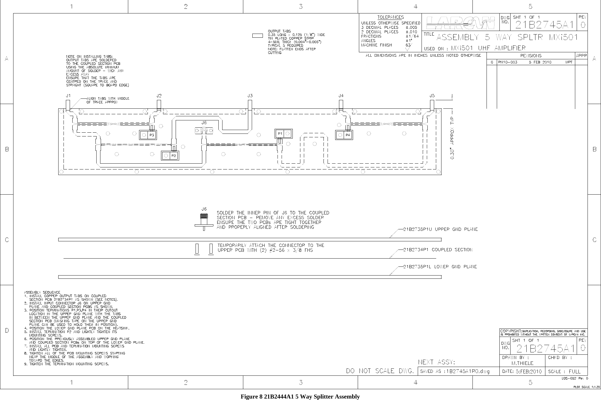
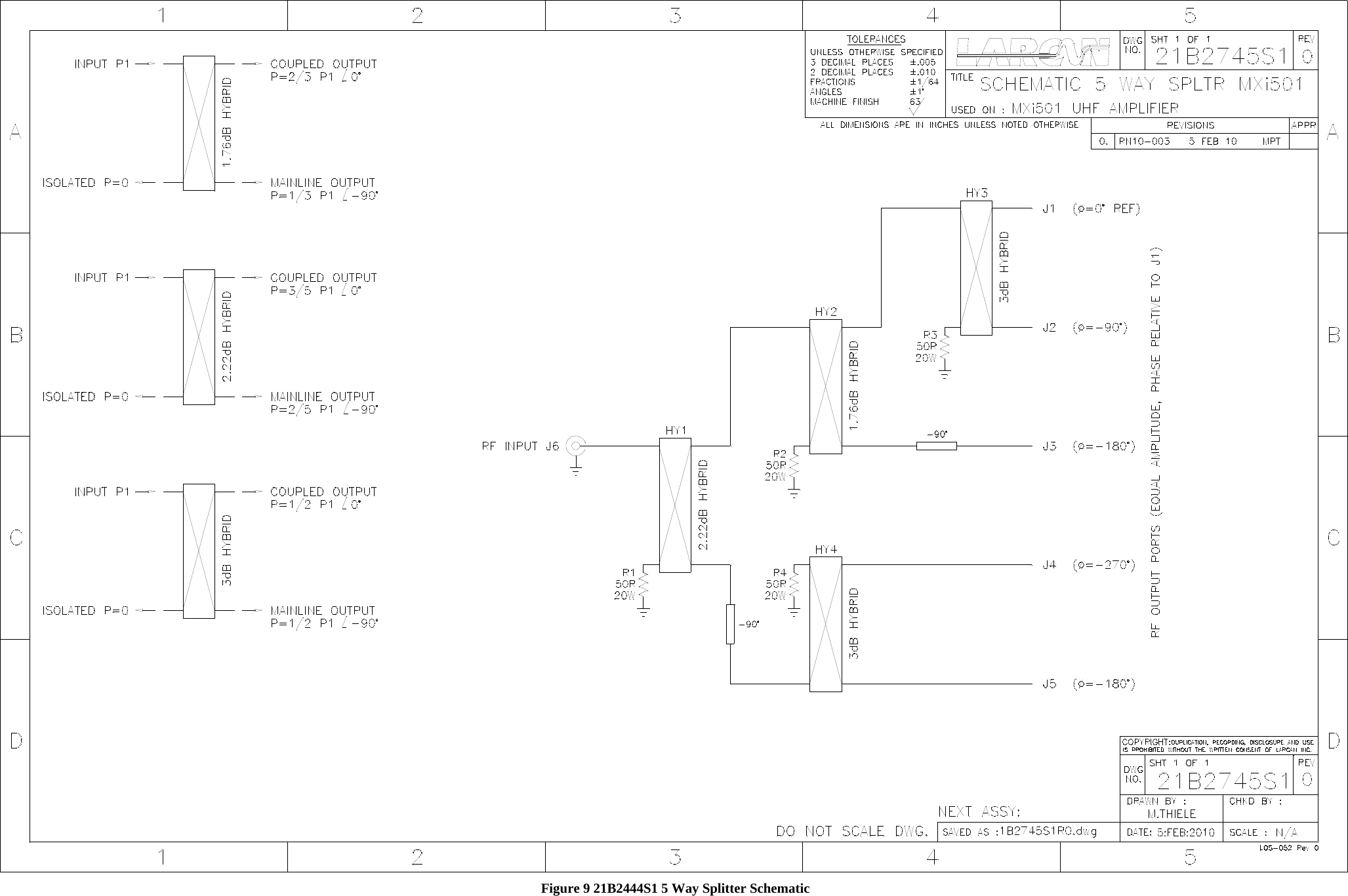
splitter
5.
control chassis
6.
Operations and maintenance
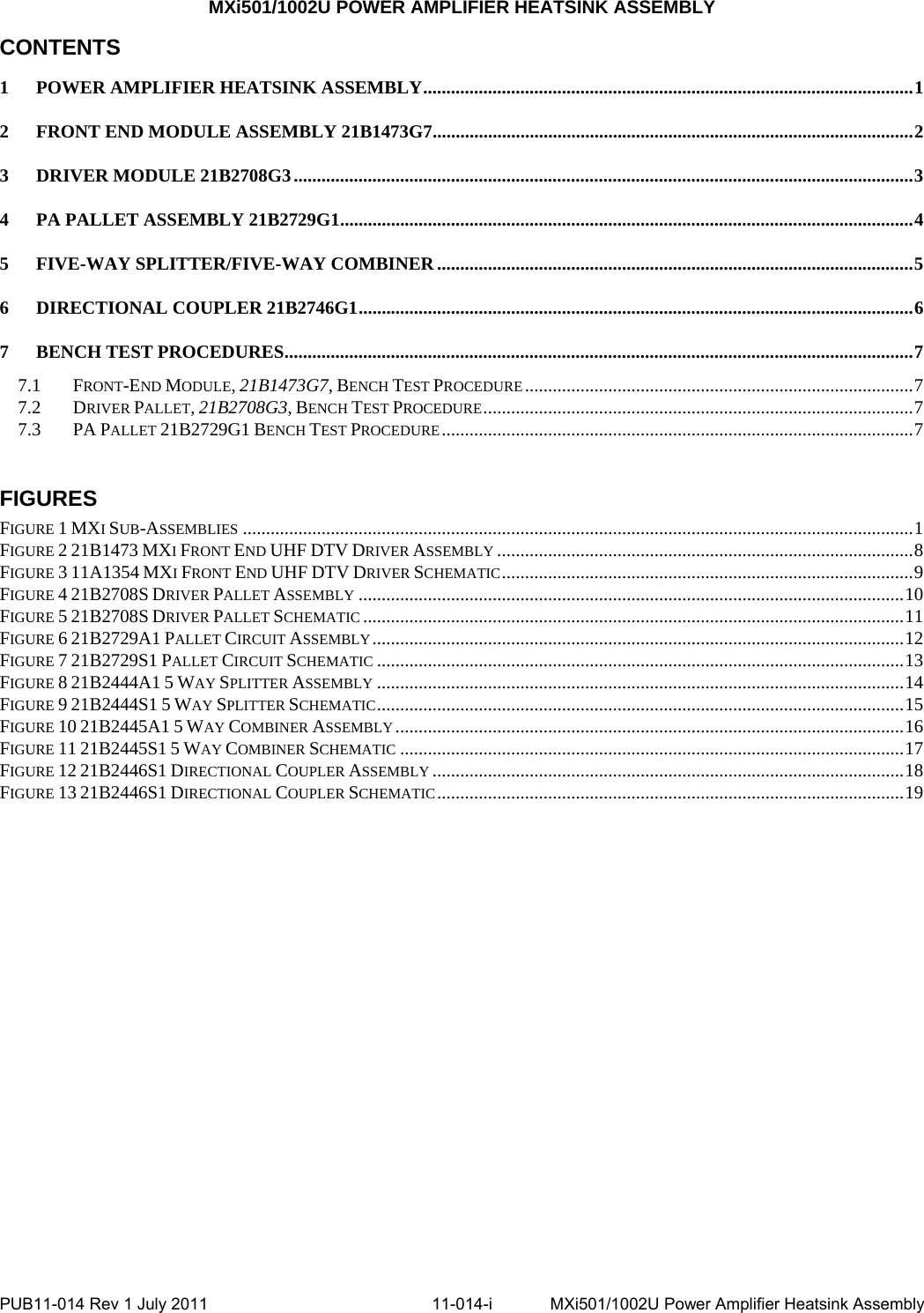
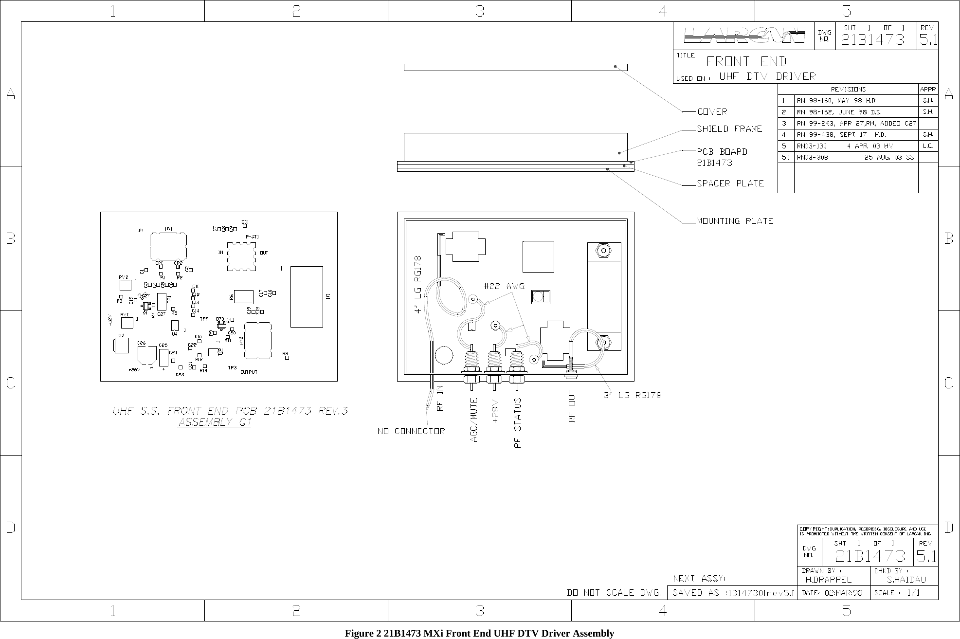
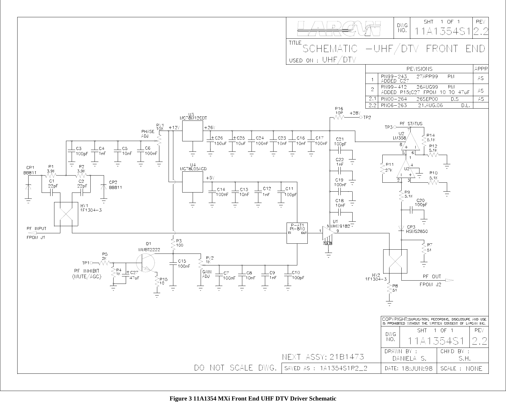
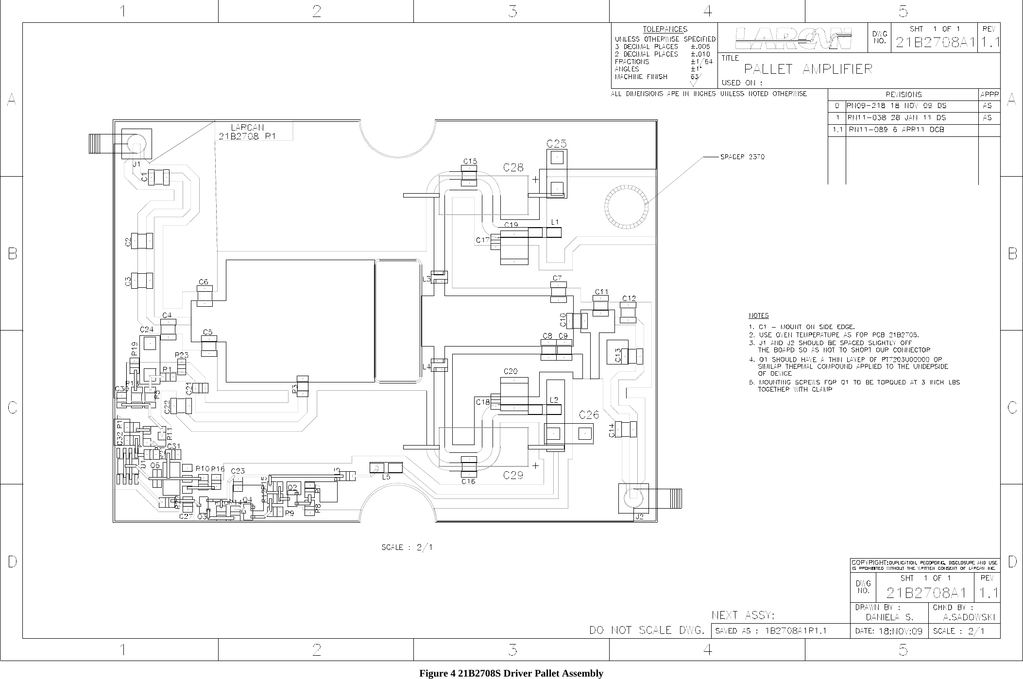
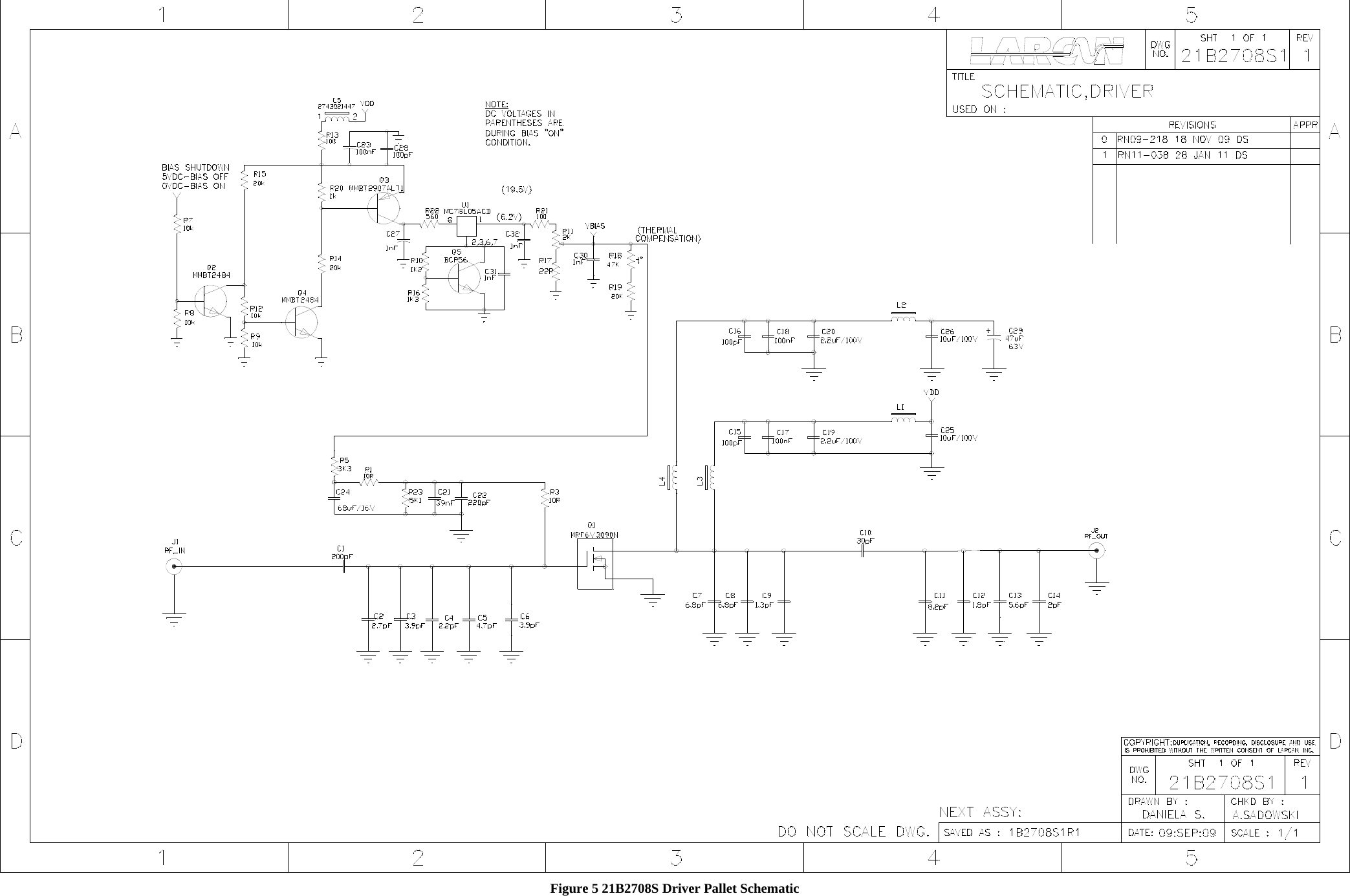
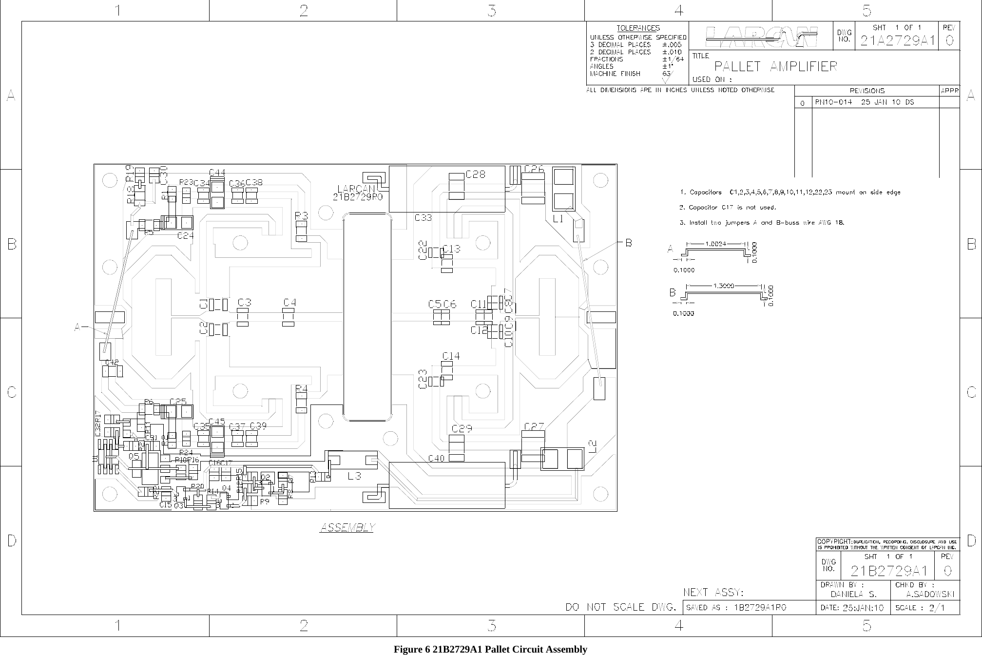
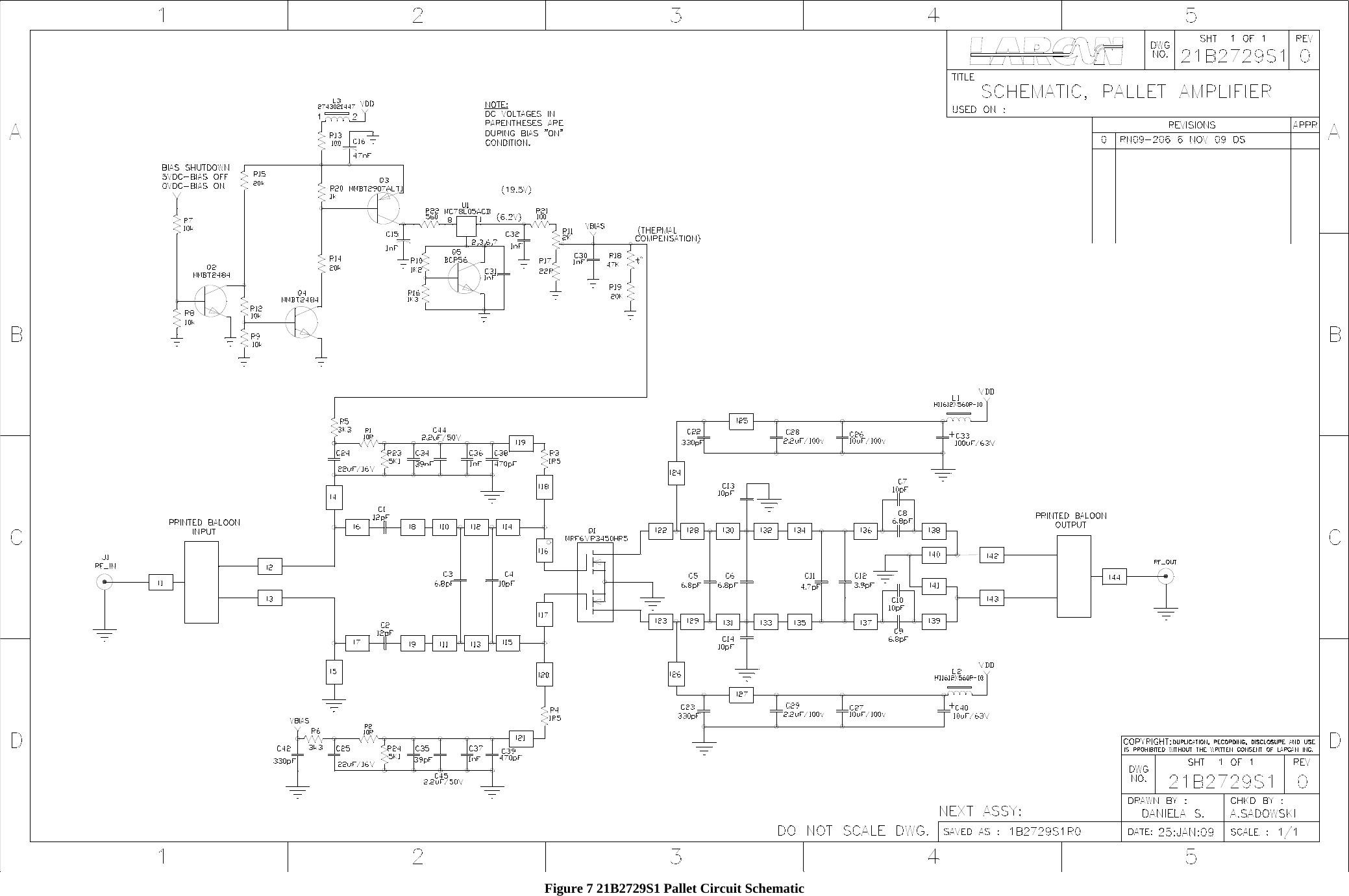
Power Amplifier
Navigation menu
Upload a User Manual
Namespaces
Wiki Guide
HTML
PDF
Info
Views
User Manual
Discussion / Help
Navigation