Leidos Innovations NORMARC7033 7033 Dual Frequency Glide Path User Manual
Lockheed Martin Air Traffic Management 7033 Dual Frequency Glide Path
Contents
- 1. Normarc 7033 Instrument Landing System Operating Manual
- 2. Normarc 7033 ILS Technical Handbook
- 3. Normarc ILS Installation and Commissioning Hanbook Vol 1
- 4. Normarc ILS Installation and Commissioning Hanbook Vol 2
- 5. Normarc ILS Installation and Commissioning Hanbook Vol 1 and 2
- 6. Normarc ILS General Description
- 7. Normarc 7033 Instrument Landing System Operation Manual
- 8. Normarc ILS Installation and Commissioning Handbook Vol 1
- 9. Normarc ILS Installation and Commissioning Handbook Vol 2
- 10. Normarc ILS Installation and Commissioning Handbook Vol 1 and 2
- 11. Normarc 7033 ILS General Description
Normarc 7033 ILS Technical Handbook

1250$5&
INSTRUMENT LANDING SYSTEM
Technical Handbook
21829-3.6
©1999 Navia Aviation AS


7(&+1,&$/+$1'%22.
1DYLD$YLDWLRQ$6
L
TECHNICAL HANDBOOK
NORMARC 7033
TABLE OF CONTENTS
1250$5&
7DEOHRIFRQWHQWV
PART I INTRODUCTION.....................................................................................1-1
1 GENERAL INFORMATION.............................................................................1-1
1.1 Introduction........................................................................................................1-1
1.1.1 ILS Overview ............................................................................................... 1-1
1.1.2 Glidepath Overview ..................................................................................... 1-1
1.1.3 Glidepath Description ..................................................................................1-2
1.2 Product Type Numbers ...................................................................................... 1-2
1.3 Abbreviations...................................................................................................... 1-3
2 PHYSICAL ORGANIZATION..........................................................................2-1
2.1 Module and Assembly Location .........................................................................2-1
2.2 Service Kit Assembly.......................................................................................... 2-1
2.3 Power Supply.....................................................................................................2-1
3 SYSTEM DESCRIPTION................................................................................3-1
3.1 Overview ............................................................................................................3-1
3.2 Physical Description........................................................................................... 3-1
3.3 Monitors.............................................................................................................. 3-2
3.4 Transmitters / Modulators...................................................................................3-2
3.5 TX Control .......................................................................................................... 3-2
3.6 Remote Monitoring (RMS) Unit ..........................................................................3-3
3.7 Remote Control Unit........................................................................................... 3-3
3.8 Remote Slave Panel........................................................................................... 3-3
3.9 Remote Maintenance Monitoring (RMM) ...........................................................3-3
3.9.1 RMM Access................................................................................................ 3-5
3.9.2 Storage Functions........................................................................................3-5
3.9.3 Local Keyboard/Display Functions ..............................................................3-5
3.9.4 Diagnostic functions..................................................................................... 3-6
4 TECHNICAL SPECIFICATIONS.....................................................................4-1
4.1 Signal Minimum Performance GP......................................................................4-1
4.2 Environmental Characteristics............................................................................ 4-2
4.3 EMC Characteristics........................................................................................... 4-2
4.4 Mechanical Characteristics ................................................................................ 4-2
4.5 Power Supply.....................................................................................................4-3

1250$5&7(&+1,&$/+$1'%22.
7DEOHRIFRQWHQWV 1DYLD$YLDWLRQ$6
LL
PART II INSTALLATION .....................................................................................5-1
5 MECHANICAL INSTALLATION......................................................................5-1
5.1 Mounting Kit MK1343A.......................................................................................5-1
5.2 Moving RF Connectors.......................................................................................5-2
6 ELECTRICAL INSTALLATION .......................................................................6-1
6.1 Connection Overview .........................................................................................6-1
6.2 Power and Battery.............................................................................................. 6-1
6.3 RF Inputs............................................................................................................6-2
6.4 RF Outputs......................................................................................................... 6-3
6.5 DC Loop (Localizer only).................................................................................... 6-4
6.6 Remote Control .................................................................................................. 6-5
6.7 PC and Modem ..................................................................................................6-6
6.8 DME (localizer only) ........................................................................................... 6-7
6.9 For the Fernau 2020 DME the following connection is recommended...............6-9
6.10 Analog Inputs .....................................................................................................6-9
6.11 Digital Inputs and Outputs..................................................................................6-11
6.12 Battery Warning.................................................................................................. 6-11
6.13 Remote control connections...............................................................................6-12
6.14 Automatic shutdown of GP................................................................................. 6-14
6.15 Remote slave connection...................................................................................6-15
6.16 Interlock switch connection ................................................................................6-16
7 TESTS AND ADJUSTMENTS ........................................................................7-1
7.1 Configuration Settings........................................................................................ 7-1
7.1.1 ILS Configuration ......................................................................................... 7-1
7.1.2 Remote Ports Access Level Configuration .................................................. 7-2
7.1.3 Warning Configuration................................................................................. 7-2
7.1.4 Remote Control Interface (CI 1210).............................................................7-2
7.1.5 Remote Control configuration...................................................................... 7-3
7.2 Technical note - Leased Line Setup for Remote Control (Westermo)................7-5
7.2.1 DIP switch settings ...................................................................................... 7-5
7.2.2 Strap settings on modems...........................................................................7-5
7.2.3 Connecting modem to the cabinet...............................................................7-5
7.2.4 Connecting modem to the RC .....................................................................7-6
7.2.5 Connecting the two modems .......................................................................7-6
7.3 Transmitter Alignments and Calibration ............................................................. 7-6
7.3.1 RF Phase Feedback Adjustment .................................................................7-6
7.3.2 RF Power..................................................................................................... 7-7
7.3.3 LF Phase Adjustment .................................................................................. 7-7
7.3.4 RF Power Balance Adjustment....................................................................7-9
7.3.5 RF Phase at Combiner I/P........................................................................... 7-9
7.3.6 SDM Calibration...........................................................................................7-10
7.3.7 DDM Calibration .......................................................................................... 7-10
7.3.8 Ident Tone Modulation Depth ......................................................................7-11
7.3.9 RF Frequency Adjustment...........................................................................7-11
7.4 Antenna System Adjustments ............................................................................7-12
7.5 Monitor Alignment and Calibration.....................................................................7-12
7.5.1 General ........................................................................................................ 7-12
7.5.2 RF Input Level Adjustment. .........................................................................7-12
7.5.3 AGC Time Adjustment................................................................................. 7-13
7.5.4 SDM Adjustment.......................................................................................... 7-14

7DEOHRIFRQWHQWV
1250$5&
LLL
1DYLD$YLDWLRQ$6
7(&+1,&$/+$1'%22.
7.5.5 DDM Adjustment.......................................................................................... 7-14
7.6 Monitor Alarm Setting Procedure .......................................................................7-14
7.7 Maintenance Limit Adjustments ........................................................................ 7-15
7.8 Adjustment points............................................................................................... 7-16
PART III DESCRIPTION......................................................................................8-1
8 FUNCTIONAL DESCRIPTION........................................................................8-1
8.1 Introduction......................................................................................................... 8-1
8.2 Transmitter ......................................................................................................... 8-2
8.3 Monitor ............................................................................................................... 8-4
8.4 Transmitter Control.............................................................................................8-4
8.5 Remote control system.......................................................................................8-6
8.6 Remote Monitoring System (RMS).....................................................................8-7
8.6.1 General Description ..................................................................................... 8-7
8.6.2 PC and Modem...........................................................................................8-7
8.6.3 RMS Databus .............................................................................................. 8-8
8.6.4 Maintenance Data Collection....................................................................... 8-8
8.7 Power Supply.....................................................................................................8-9
9 DETAILED DESCRIPTION.............................................................................9-1
9.1 Main Cabinet ...................................................................................................... 9-1
9.1.1 MF1219A Glidepath Monitor Frontend ........................................................ 9-1
9.1.2 MO1212A Monitor........................................................................................9-4
9.1.3 TCA1218A Transmitter Control Assembly...................................................9-8
9.1.4 LF1223A Low Frequency Generator ...........................................................9-17
9.1.5 OS1221B RF Oscillator ............................................................................... 9-18
9.1.6 GPA1231A Glidepath Course Power Amplifier Assembly...........................9-20
9.1.7 GPA1232A Glidepath Clearance Power Amplifier Assembly ...................... 9-21
9.1.8 COA1207C Change-Over Assembly ...........................................................9-29
9.1.9 PS1227A Power Supply .............................................................................. 9-29
9.1.10RMA1215A RMS Assembly.........................................................................9-30
9.1.11CI1210A External Connection Interface ......................................................9-32
9.1.12MB1203A Monitor Section Motherboard...................................................... 9-33
9.2 Tower Equipment ............................................................................................... 9-34
9.2.1 RCA1240C Remote Control Assembly........................................................ 9-34
9.2.2 Motherboard MB1346A................................................................................9-37
9.2.3 Power Supply PS635B ................................................................................9-37
9.2.4 Motherboard MB1347A................................................................................9-37
9.2.5 Slave Panel SF1344A and SP1394A ..........................................................9-38
9.2.6 IL1379 / IL1380 Interlock switch ..................................................................9-38
10 PARTS LISTS .................................................................................................10-1
10.1 Introduction......................................................................................................... 10-1
10.1.1Explanation of Parts Lists Form...................................................................10-1
10.2 Parts Lists ....................................................................................................... 10-2
10.3 Usable on code index......................................................................................... 10-3
10.4 Figures ............................................................................................................... 10-3
PART IV APPENDIXES.......................................................................................A-1
A CUSTOMERS INFORMATION.......................................................................A-1


7(&+1,&$/+$1'%22.
1DYLD$YLDWLRQ$6
L
LIST OF FIGURES
1250$5&
/LVWRI)LJXUHV
Figure 1-1 Typical ILS installation...........................................................................1-1
Figure 1-2 Glidepath block diagram........................................................................1-2
Figure 2-1 NM 7033 Module Location - Front view.................................................2-2
Figure 2-2 NM 7033 Module Location - Rear view of main section. .......................2-3
Figure 2-3 NM 7033 Module Location - Front view of wall-mounted section..........2-4
Figure 3-1 ILS block diagram..................................................................................3-1
Figure 3-2 The NM 7000 series RMM/RMS systems. ............................................3-4
Figure 5-1 NM 70XX required mounting space (top view)......................................5-1
Figure 5-2 NM 70XX mounted on wall with MK1343A............................................5-2
Figure 5-3 Moving the RF connectors to the cabinet bottom..................................5-3
Figure 6-1 ILS main cabinet connection overview..................................................6-1
Figure 6-2 Power and backup battery connections. ...............................................6-2
Figure 6-3 RF input connections.............................................................................6-3
Figure 6-4 RF output connections. .........................................................................6-3
Figure 6-5 DC loop connections. ............................................................................6-4
Figure 6-6 Remote control connection....................................................................6-5
Figure 6-7 PC and modem connections. ................................................................6-6
Figure 6-8 DME connections. .................................................................................6-7
Figure 6-9 DME master connections. .....................................................................6-8
Figure 6-10 LLZ master connections. .......................................................................6-8
Figure 6-11 LLZ Main connections Fernau 2020 DME.............................................6-9
Figure 6-12 Analog input connections. .....................................................................6-10
Figure 6-13 Digital input/output connections. ...........................................................6-11
Figure 6-14 Battery warning connections. ................................................................6-12
Figure 6-15 Remote control to ILS connection .........................................................6-13
Figure 6-16 Remote control power supply connections............................................6-14
Figure 6-17 Automatic GP shutdown connection .....................................................6-15
Figure 6-18 Remote slave connection ......................................................................6-16
Figure 6-19 Interlock switch connection ...................................................................6-16
Figure 7-1 Station Control strap platform................................................................7-2
Figure 7-2 Cable connections for Remote Control via RS-232...............................7-3
Figure 7-3 LF phase CSB illustration......................................................................7-7
Figure 7-4 LF phase SBO illustration......................................................................7-8
Figure 7-5 Power balance SBO illustration.............................................................7-9
Figure 7-6 RF phase SBO illustration .....................................................................7-10
Figure 7-7 Adjustment points on Monitor Frontend MF12xx...................................7-13
Figure 7-8 Alternative jumper settings of P2++ ......................................................7-13
Figure 7-9 Front side adjustment points. ................................................................7-16
Figure 7-10 CI1210A Connection Interface adjustment point...................................7-17
Figure 7-11 Power Amplifier Assembly adjustment points (rear view)......................7-18
Figure 8-1 ILS Block Diagram.................................................................................8-2
Figure 8-2 System Block Diagram of a 2-Frequency GP Transmitter.....................8-3
Figure 8-3 Monitor section block diagram...............................................................8-4
Figure 8-4 TCA1218A/B Block Diagram.................................................................8-5
Figure 8-5 RCA1240A/B Block Diagram.................................................................8-6
Figure 8-6 The RMM configuration.........................................................................8-7
Figure 8-7 The RMS databus. ................................................................................8-8
Figure 8-8 The IIC serial bus and ADC channels. ..................................................8-9
Figure 8-9 Power supply functional diagram. .........................................................8-10
Figure 9-1 MF1219A Block diagram (CL channel shown) ......................................9-3

1250$5&7(&+1,&$/+$1'%22.
/LVWRI)LJXUHV 1DYLD$YLDWLRQ$6
LL
Figure 9-2 MO1212A Blockdiagramm ....................................................................9-7
Figure 9-3 TCA1218A Block diagram part 1...........................................................9-15
Figure 9-4 TCA1218B Block diagram part 2...........................................................9-16
Figure 9-5 NMP110A block diagram.......................................................................9-18
Figure 9-6 OS1221B block diagram. ......................................................................9-19
Figure 9-7 Physical organisation of power amplifier assembly...............................9-26
Figure 9-8 NM 7033 Transmitter Block Diagram part 1 ..........................................9-27
Figure 9-9 NM 7033 Transmitter Block Diagram part 2 ..........................................9-28
Figure 9-10 Changeover system block diagram. ......................................................9-29
Figure 9-11 PS1227A Block Diagram.......................................................................9-30
Figure 9-12 RMA1215A Block Diagram....................................................................9-31
Figure 9-13 CI1210A Block diagram.........................................................................9-33
Figure 9-14 Block diagram RCA1240C ....................................................................9-35
Figure 9-15 Block diagram NMP128A ......................................................................9-36
Figure 9-16 Interlock switch connections..................................................................9-39
Figure 10-1 Intensionally omitted..............................................................................10-3
Figure 10-2 Intenionally omitted ...............................................................................10-3
Figure 10-3 Normarc 7011 & 7033 LLZ & GP cabinet, wall mount side...................10-3
Figure 10-4 Normarc 7033 GP cabinet.....................................................................10-4
Figure 10-5 Normarc 7033 GP cabinet, Rear view...................................................10-5

7(&+1,&$/+$1'%22.
1DYLD$YLDWLRQ$6
L
LIST OF TABLES
1250$5&
/LVWRIWDEOHV
Table 7-1 ILS configuration settings. ...................................................................7-1
Table 7-2 Access level strap settings..................................................................7-2
Table 7-3 Remote Control Setup.........................................................................7-2
Table 7-4 Aural warning configuration.................................................................7-4
Table 7-5 Warning reset (Silence):......................................................................7-4
Table 7-6 Buzzer: ................................................................................................7-4
Table 7-7 Telephone Line / RS 232 / TTL logic:.................................................. 7-4
Table 7-8 Normal operating power level..............................................................7-7
Table 7-9 Localizer alarm limits...........................................................................7-14
Table 7-10 Glidepath alarm limits..........................................................................7-15
Table 9-1 MB1203A plug in module connectors..................................................9-34

*(1(5$/,1)250$7,21
1250$5&
1DYLD$YLDWLRQ$6
7(&+1,&$/+$1'%22.
3$57,,1752'8&7,21
1 General Information
This paragraph gives a description of a typical ILS installation and the Normarc Glidepath sys-
tem. Conventions and abbreviations used in this manual are also given.
1.1 Introduction
This is an overview of Normarc’s NM703X ILS glidepath systems.
1.1.1 ILS Overview
A complete Instrument Landing System comprises:
• A LOCALIZER SYSTEM, producing a radio course to furnish lateral guidance to the airport
runway.
• A GLIDE PATH SYSTEM, producing a radio course to furnish vertical guidance down the
correct descent angle to the runway.
• MARKER BEACONS, to provide accurate radio fixes along the approach course.
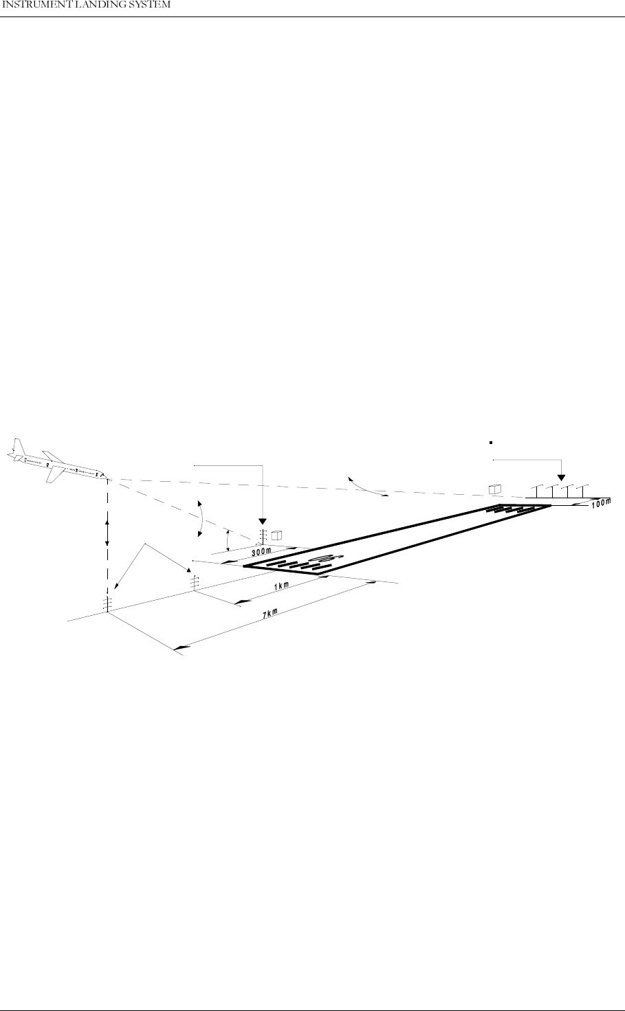
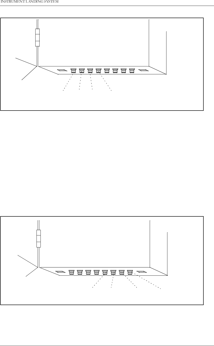
The layout of a typical ILS airport installation is shown below.
Figure 1-1 Typical ILS installation
1.1.2 Glidepath Overview
The complete ILS Glidepath system comprises:
• A GP transmitter/monitor cabinet
• An antenna distribution network
• A monitor network
• A GP antenna array
• Near-field monitor antenna
Localizer
110 MHz
Glide Path
330 MHz
Marker Beacon
75MHz
3°
HBK547-1
1250$5&7(&+1,&$/+$1'%22.
*(1(5$/,1)250$7,21 1DYLD$YLDWLRQ$6
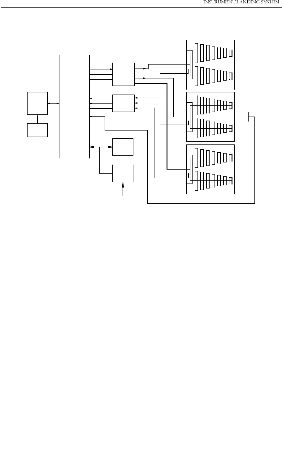
A block diagram is shown below:
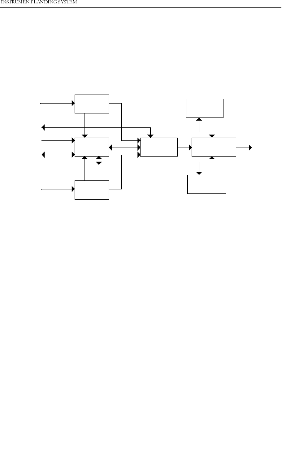
Figure 1-2 Glidepath block diagram
1.1.3 Glidepath Description
To shape the glide path signal, ground plane reflection from an area in front of the antenna
array is necessary. The specific requirements to the area are given in the antenna handbook.
The glide path site may be located on either side of the runway, but the most reliable operation
will be obtained if the site is selected on terrain least obstructed by taxiways, aircraft holding
aprons, parking ramps, buildings, power lines etc. The site should offer the widest area of
smooth ground with possibilities of levelling without excessive physical or economical effort, if
indeed levelling is deemed necessary.
The glide path antenna system should be located at a distance of 75-200 m from the runway
center line. The distance from the runway threshold is a function of several factors upon which
establishment of the optimum operational conditions depend. These factors are:
1. The glide path angle.
2 Threshold crossing height requirements.
3. Obstruction clearance requirements
4 The slope of the terrain in front of the antenna system.
5. The extent of smooth terrain in the site area and beyond the threshold.
1.2 Product Type Numbers
The Normarc product numbering system is based on the following three levels:
GP-BLOCK DIAGRAM
HBK205-1
TRANSMITTER
AND
MODULATOR
I and II
MONITOR
I and II
REMOTE
CONTROL
UNIT
SLAVE
PANEL
CSB CL
SBO CL
CSB CLR*
CL
CLR*
DS
NF
ANTENNA
DISTRIBU-
TION NETW.
**
MONITOR
NETWORK
24V
BATTERY
SUPPLY
POWER
MAINS INPUT
220V/110V AC
U
L
M
ILS Localizer
and Glide Path
GP
TRANSMITTER
***
* CLR signals only used for 2-frequency systems.
** Antenna distribution network not used for Null Reference.
*** Middle antenna used for M-Array and Modified M-Array.

*(1(5$/,1)250$7,21
1250$5&
1DYLD$YLDWLRQ$6
7(&+1,&$/+$1'%22.
•System
• Assembly
• Module
Systems have type numbers starting with NM, for example NM 7033. Systems consist of
assemblies, modules and parts.
Assemblies have type numbers consisting of three letters, a three- or four- digit number and a
letter, for example LPA 1230A. LPA is an abbreviation of
L
ocalizer
P
ower amplifier
A
ssembly,
1230 is a running number, and the last letter is the variant designator. Assemblies can consist
of assemblies, modules and parts.
Modules have type numbers consisting of two letters, a three- or four- digit number and a let-
ter, for example FD 1235A. FD is an abbreviation of
F
eedback
D
etector, 1235 is a running
number, and the last letter is the variant designator. Modules consist of parts.
1.3 Abbreviations
AC Alternating Current
ADC Analog to Digital Converter
AGC Automatic Gain Control
CL Course Line
CLR Clearance
COU Course
CPU Central Processing Unit
CS Course Sector
DAC Digital to Analog Converter
DC Direct Current
DDM Difference in Depth of Modulation
DF Difference Frequency
DL Dc Loop
DS Displacement Sensitivity
DSP Digital Signal Processor
EEPROM Electrically Erasable Progammable Read Only Memory
EMC ElectroMagnetic Compatibility
EMI ElectroMagnetic Interference
EPROM Erasable Programmable Read Only Memory
FFT Fast Fourier Transform
FIFO First-In-First-Out
FPGA Field Programmable Gate Array
GPA Glidepath Power amplifier Assembly
I/F InterFace
I²C Inter Integrated Circuit
IIC Same as I²C
ILS Instrument Landing System
LED Light Emitting Diode
LF Low Frequency
LLZ Localizer
LPA Localizer Power amplifier Assembly
LRU Line Replacable Unit
MCU Monitor Combiner Unit

1250$5&7(&+1,&$/+$1'%22.
*(1(5$/,1)250$7,21 1DYLD$YLDWLRQ$6
NAV NAVigation signals
NF Near Field
PC Personal Computer
RAM Random Access Memory
RF Radio Frequency
RMM Remote Maintenance Monitor
RMS Remote Monitoring System
ROM Read Only Memory
RTC Real Time Clock
SC Station Control
SDM Sum in Depth of Modulation
SPA Same Parameter Alarm
SRAM Static Random Access Memory
STB Standby
SW SoftWare
TRM TeRMinator
TX Transmitter

3+<6,&$/25*$1,=$7,21
1250$5&
1DYLD$YLDWLRQ$6
7(&+1,&$/+$1'%22.
2 Physical Organization
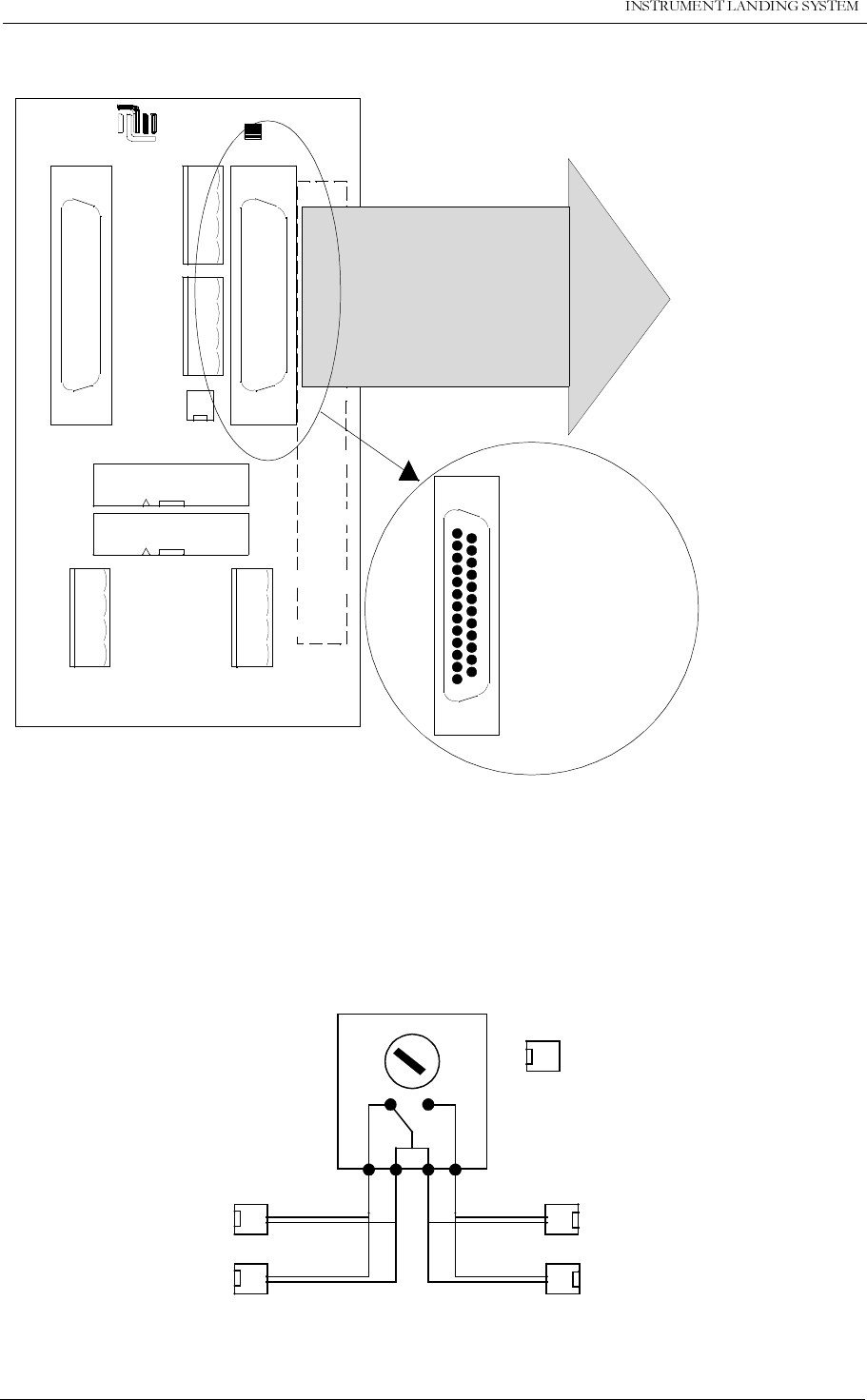
2.1 Module and Assembly Location
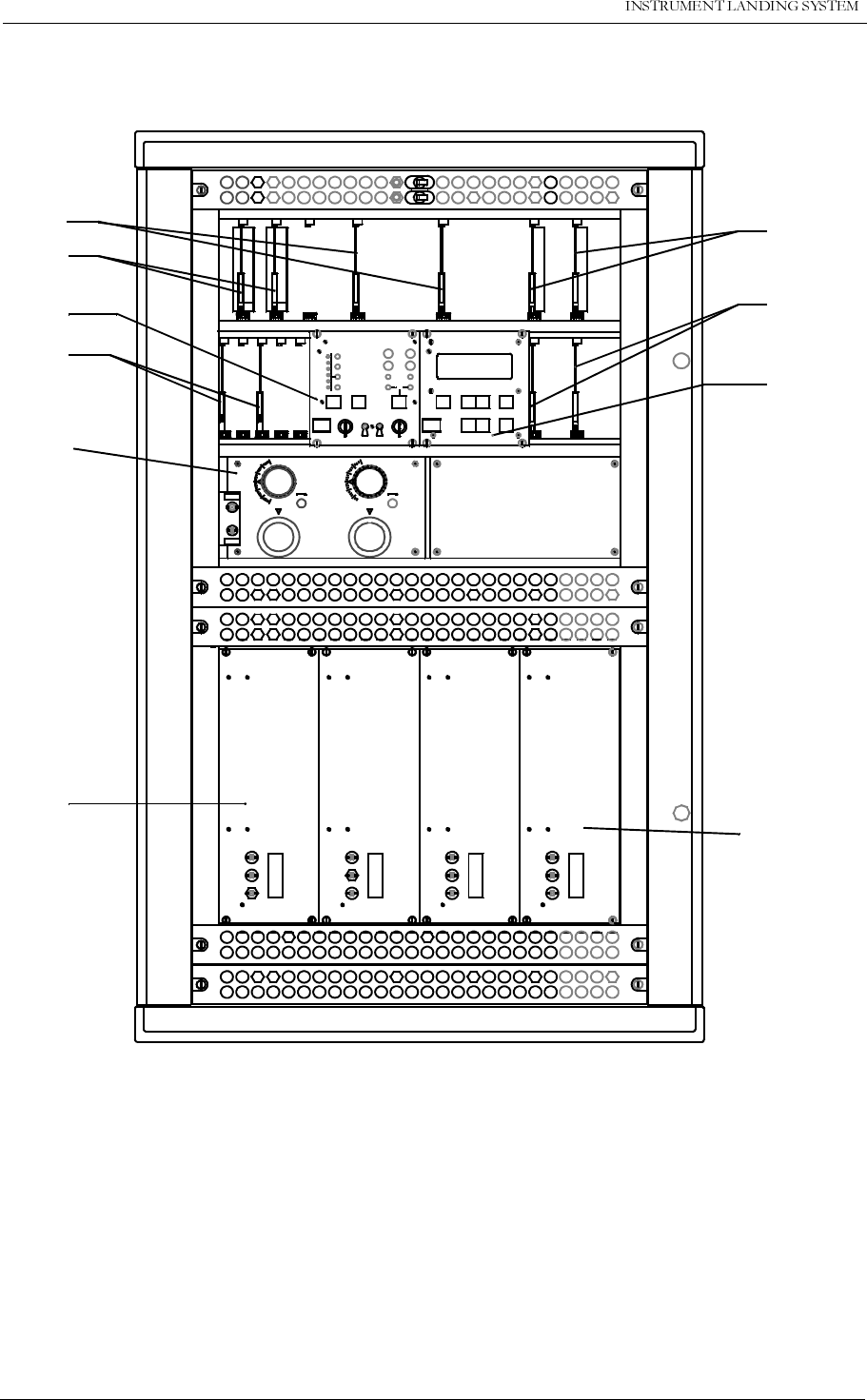
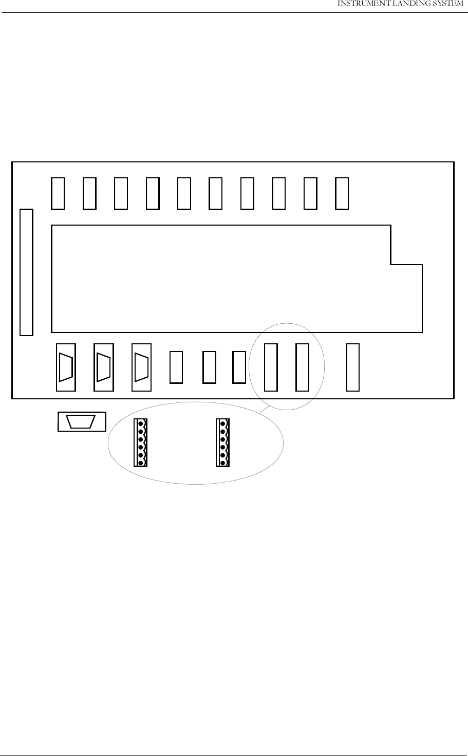
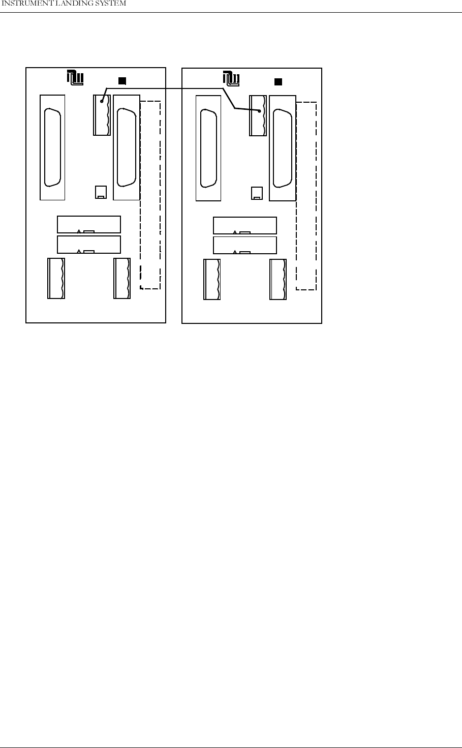
The figures on the following pages show the locations of the modules in the main cabinet.
Figure 2-1 shows the main section of the GP cabinet from a front view, with indications of the
plug-in board locations.
Figure 2-2 shows the same section from a rear view, while Figure 2-3 shows the top half of the
wall-mounted section.
In addition, the Remote Control Assembly RCA1240C/D and Remote Slave SF 1344A are
installed in the technical control room and the control tower, respectively.
2.2 Service Kit Assembly
The Service Kit Assembly SKA 1229A includes two different extension boards for mainte-
nance operations:
EB1349A Extension Board - for use with the Power Supply PS1227A, Monitor
MO1212A, RMS Assembly RMA1215A, Transmitter Control Assembly
TCA1218A/B and Low Frequency Generator LF1223A plug-in boards.
EB1245A Extension Board with coax cables - for use with Monitor Frontend MF1219A
and Oscillator OS1221B plug-in boards.
In addition, the following items are included:
• Static-dissipative work mat and wrist strap to ensure ESD-protected environment when
performing maintenance operations on the equipment.
• Torque wrench, screw drivers etc.
2.3 Power Supply
An External Power Supply, operating at 230V/120V mains input and providing 27V at 20A, is
normally supplied with the equipment. In special cases, a second external power supply is
supplied.
3+<6,&$/25*$1,=$7,21
1250$5&
1DYLD$YLDWLRQ$6
7(&+1,&$/+$1'%22.
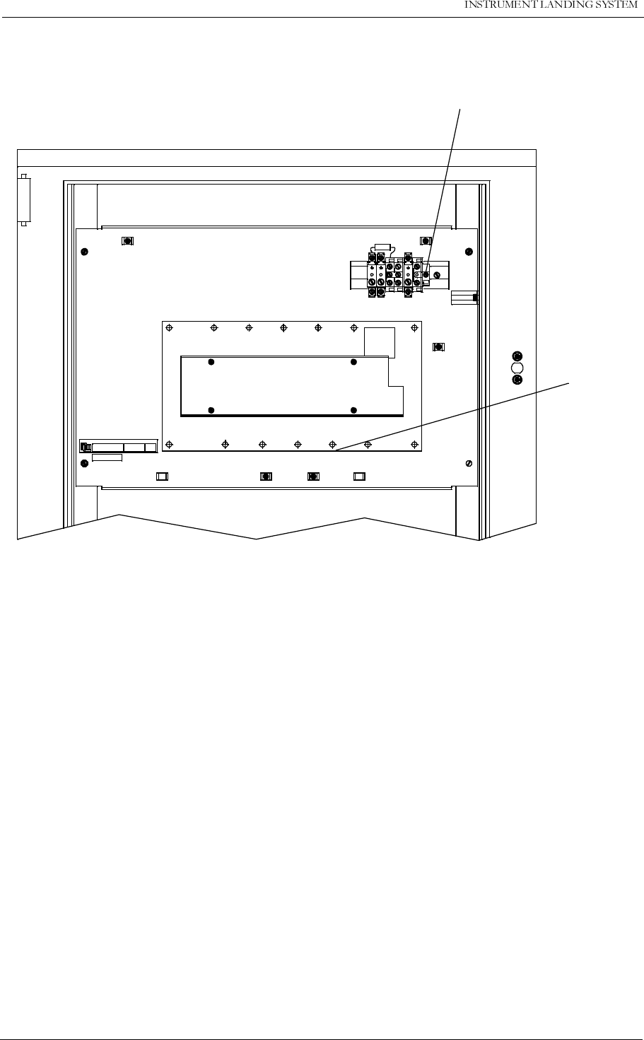
Figure 2-2 NM 7033 Module Location - Rear view of main section.
SBO 1
IN IN OUT
SBO 2 SBO
DUMMY OUT
SBO CSB
DUMMY IN
CSB SBO 1
IN OUT
SBO 2 SBO
DUMMY OUT
SBO CSB
DUMMY
CSB
MB 1203
COA 1207C
TX1
CL
TX2
CL
TX1
CLR
TX2
CLR
AA
VIEW A-A
HBK 593-1
6<67(0'(6&5,37,21
1250$5&
1DYLD$YLDWLRQ$6
7(&+1,&$/+$1'%22.
3 System description
This chapter gives a functional overview of the NM70xx ILS systems.
3.1 Overview
The complete ILS electronic system is housed in a compact, wall mounted cabinet. The cabi-
net and the electronics, except for RF units, are common to the LLZ and GP systems.
Figure 3-1 ILS block diagram.
The ILS cabinets can be configured for Cat I, Cat II, or Cat III requirements with no basic
changes.
Eight models are available:
NM 7011 Single frequency LLZ
NM 7012 Single frequency LLZ with hot standby monitoring (Cat III)
NM 7013 Two frequency LLZ
NM 7014 Two frequency LLZ with hot standby monitoring (Cat III)
NM 7031 Single frequency GP
NM 7032 Single frequency GP with hot standby monitoring (Cat III)
NM 7033 Two frequency GP
NM 7034 Two frequency GP with hot standby monitoring (Cat III)
The system is based on modern technology with extensive Remote Monitoring and Mainte-
nance capabilities, and very high reliability and integrity. To meet this objective, the monitor
comparator and station control are based on digital hardware, while the RMS interface is
microprocessor based.
3.2 Physical Description
The cabinet contains three sections:
• The electronics card cage
• The change-over section
• The transmitter / PA section
The electronics card cage contains the RF oscillators, the LF signal generators, the monitors,
the station control, the RMS processor, and the voltage regulators.
Monitor
RMS
Monitor
TX control Changeover
Section
Monitor
input
signals
Monitor
input
signals Transmitter
Transmitter
NAV
signals
out
Remote
Control
External
sensors
Comm.
ports
Data and
diagnostics
HBK573-1

1250$5&7(&+1,&$/+$1'%22.
6<67(0'(6&5,37,21 1DYLD$YLDWLRQ$6
The change-over section contains coaxial relays, attenuators and phasers for the RF outputs.
The transmitter / PA section contains the PA blocks including couplers etc. for each output.
The cabinet is divided in two parts, with the rear part fixed to a wall, and the front part hinged
to give access to interior of the cabinet.
All external connections are made to the rear part of the cabinet.
3.3 Monitors
The ILS has duplicated monitors with inputs for Course Line (CL), Displacement Sensitivity
(DS), Near Field (NF), and Clearance (CLR) (Dual Freq. only). The signals are detected by
the input stage, and then digitized. In the next block they are filtered by a Fast Fourier Trans-
form performed by a signal processor. The results for each parameter is then compared with
stored limits in a digital hardware comparator.
Each of the two monitors consists of two modules. For Cat III use, Hot Standby monitoring can
be added by using one additional monitor and associated RF couplers and combiners.
The design of the monitors ensures a very high integrity due to the use of digital hardware for
the alarm comparators and a very simple Fast Fourier filtering with a signal processor. In addi-
tion, the monitor is checked by automatic self-tests.
The alarm limits are stored locally in EEPROM, and can be updated from the RMS processor,
with a separate hardware write protection to ensure that the integrity is not affected by the
RMS system.
3.4 Transmitters / Modulators
The transmitters are duplicated, either single frequency or dual frequency. Each transmitter
consists of a RF oscillator, a LF generator, and one or two PA blocks (single or dual fre-
quency).
The RF oscillator uses a synthesizer for easy frequency changes and simple logistics. The
oscillator has two outputs for use in dual frequency systems.
The LF generator contains the generators for 90Hz, 150Hz and 1020Hz signals, the ident
keyer / sequencer and interface for DME master or slave keying. All signals are generated by
division from a common clock oscillator, ensuring very stable phase relations between the
modulation signals.
The modulation balance, modulation sum, RF level and Ident morse code are set in this mod-
ule by means of multiplying digital to analog converters. The values are stored locally in
EPROM and can be updated from the RMS processor with hardware write protection.
The same LF generator is used for single and dual frequency systems.
3.5 TX Control
The TX control unit controls the system dependent on alarms from the monitors and inputs
from the local control, the remote control and, optionally, the RMS system. It also generate
status information to the same units. The local control and status indicators are a part of the

6<67(0'(6&5,37,21
1250$5&
1DYLD$YLDWLRQ$6
7(&+1,&$/+$1'%22.
TX Control unit.
All functions in the TX Control are based on digital hardware to ensure the highest integrity.
3.6 Remote Monitoring (RMS) Unit
The RMS unit contains the system microprocessor. It handles storage and read-out of monitor
parameters, measurements for maintenance and fault finding, and performs fault analysis to
isolate faults to line replaceable modules. It is also used to set monitor limits and transmitter
adjustments.
The RMM handles communication to local and remote RMS computers, and in addition it han-
dles a small display and keyboard for parameter setting and readout.
3.7 Remote Control Unit
The remote control unit is used in the tower or in the technical control room. It has indicators
for operating status as well as detailed warnings and an aural alarm device with reset. It can
control equipment on/off and change-over, and has an Access Grant-switch to allow remote
control from the RMS system.
The Remote Control Unit is connected to the ILS by one telephone pair cable.
3.8 Remote Slave Panel
The slave panel is connected to the remote control by a multipair wire. It is intended for use in
the control tower. It has indicators for normal / warning / alarm and has an aural alarm device.
in addition it can turn the equipment on and off, and has an aural alarm reset.
Optionally a slave panel with remote control functionality can be delivered.
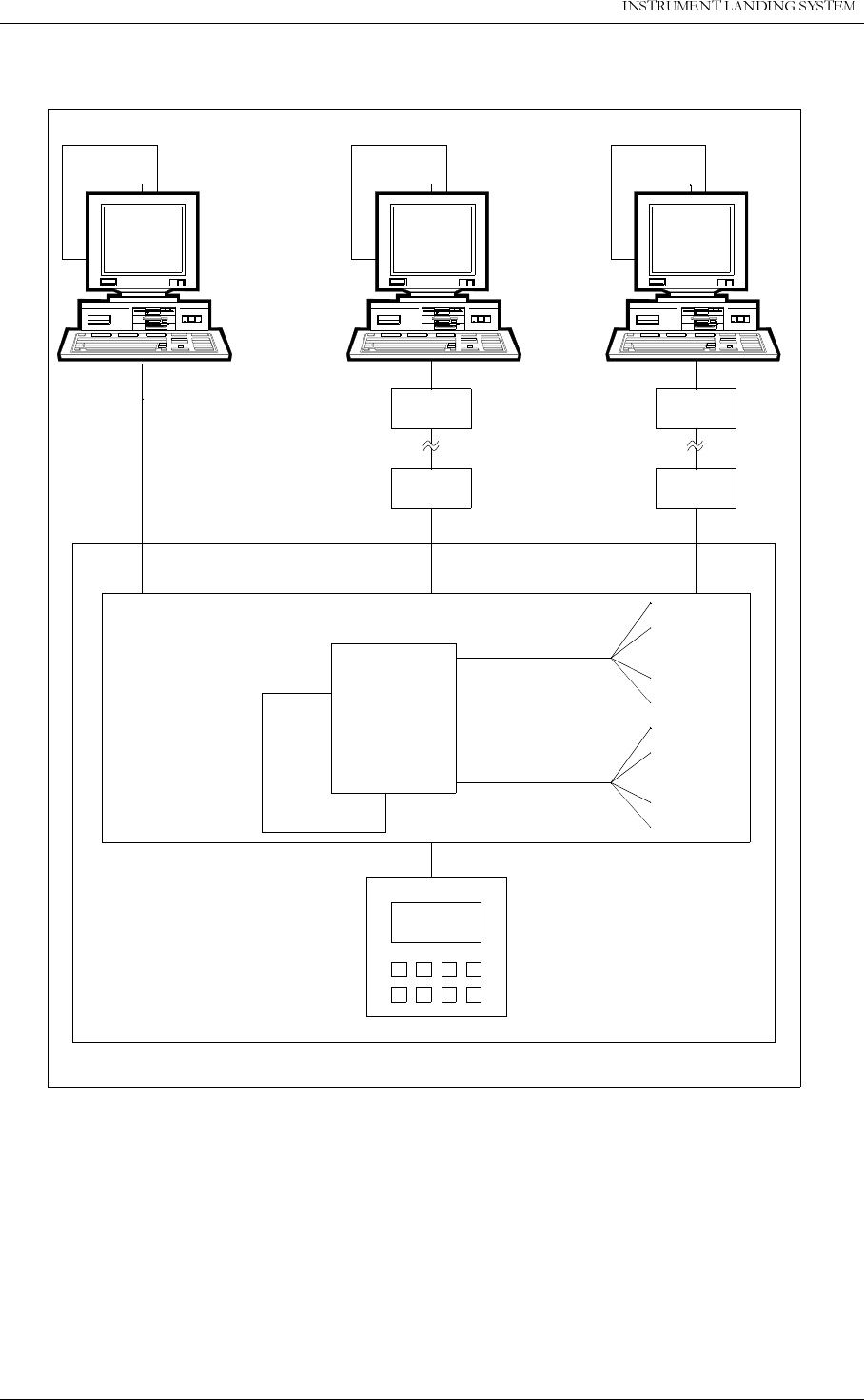
3.9 Remote Maintenance Monitoring (RMM)
The NM7000 series has a built-in Remote Maintenance Monitoring system. This system con-
sists of the RMS system, remote PC terminals with the RMM program installed, and the local
keyboard/display. Figure 3-2 illustrates the RMM/RMS systems
1250$5&7(&+1,&$/+$1'%22.
6<67(0'(6&5,37,21 1DYLD$YLDWLRQ$6
.
Figure 3-2 The NM 7000 series RMM/RMS systems.
The centre of the RMS system is a CPU with the RMS core program. The RMS collects mea-
surements and diagnostic data, and makes them available to the user. The collected informa-
tion allows easy and cost effective maintenance, fault finding and routine reporting. In
addition, system settings are distributed and parameter readings are collected via the RMS/
CPU.
External personal computers are used for a user-friendly interface to the RMM system. The
equipment has three serial output ports, typically used to connect a local PC, a PC in the air-
port technical equipment room, and a modem for connection to a central maintenance facility.
RMS
hardware
RMS
core
program
Local
measuring
points
Maintenance
data bus
RMS
data bus
Local
parameter
storages
Local
Keyboard/
Display
Modem
NM70xx
RMS system
RMM system
Local Remote 1 Remote 2
RMM
program RMM
program RMM
program
Modem Modem
Modem
HBK 598-1

6<67(0'(6&5,37,21
1250$5&
1DYLD$YLDWLRQ$6
7(&+1,&$/+$1'%22.
The local keyboard/display allow readings and control through an LCD display and a seven-
button keypad. This gives access to the RMM functionality without the need for a PC.
3.9.1 RMM Access
Access to the RMM system is controlled by multiple hardware and software access controls.
One password is required for each access level, i.e. one password for level 1, two for level 2
and three for level 3. Optional hardware controls may inhibit writing in the upper access levels.
Access level 1
• Readout of all the monitor values, warning and alarm limits.
• Readout of all the maintenance values and warning limits.
• Readout of all the delays.
• Readout of all the monitor DDM offsets.
Access level 2
• TX1 and TX2: 90/150 Hz on/off.
• TX1 and TX2: morse normal, continuous, TST or off.
• TX1 and TX2: test-signal 90 Hz or 150 Hz dominance on/off.
• Diagnostics.
Access level 3
• Settings of all the monitor warning and alarm limits.
• Settings of all the maintenance warning limits.
• Settings of all the delays.
• Settings of all the monitor DDM offsets.
3.9.2 Storage Functions
The RMS has the following storage functions:
Alarm storage:
• Contains data for the last four alarms. Each set contains data for the last 30 seconds
before and
immediately after
the alarm occurred. The last 6 seconds are sampled at a 0.1
sec. rate, the rest at 5 sec. intervals.
Warning storage:
• Contains one data set for each of the last 25 warnings that have occurred.
Medium time periodic storage:
• Contains one data sets at 15 minutes intervals for the last 24 hours.
Long time periodic storage:
• Contains average value and standard deviation of the data sets for each 24 hour period in
the last 180 days.
Event storage:
• Stores the last 50 major operational events, including user logins and logouts, TX on/off
operations, alarms and warnings, monitor parameter changes and changes in system sta-
tus.
3.9.3 Local Keyboard/Display Functions
Through a menu-based interface all main commands, adjustments and monitor limits are

1250$5&7(&+1,&$/+$1'%22.
6<67(0'(6&5,37,21 1DYLD$YLDWLRQ$6
accessible from the front panel keypad and LCD display. In addition a quick-read function
gives read-out of all main monitor parameters in a glance.
3.9.4 Diagnostic functions
The system contains internal measuring points and diagnostic functions to isolate faults to
failed modules. The values measured are referred to as
maintenance parameters
. Please
refer to the NM70xx Operating Manual.

7(&+1,&$/63(&,),&$7,216
1250$5&
1DYLD$YLDWLRQ$6
7(&+1,&$/+$1'%22.
4 Technical Specifications
NM 7033 Two-Frequency Glidepath Cabinet
4.1 Signal Minimum Performance GP
Transmitter
Frequency range 328.6-335.4 MHz
Frequency tolerance + 0.002%
Output power (CSB + SBO) Course 3-7 W adjustable
Output power (CSB) Clearance 0.3-1 W adjustable
Harmonic radiation 2.5 uW maximum
RF difference frequency (2-freq. only) 15 kHz + 5 kHz
Spurious 25 uW maximum
Output power stability + 0.2 dB
CSB/SBO stability + 0.3 dB
Modulator - Course line
Modulation depth 90/150 Hz 40%
adjustable range 10-44%
SDM stability + 0.8% SDM
DDM stability + 0.2% DDM
Frequency tolerance + 0.05 Hz
Total harmonic dist. (90/150 Hz) 1% maximum
Phase locking (90 Hz to 150 Hz) 5° maximum ref 150 Hz
SBO phaser adjustment range + 30°
Modulator - Clearance
Modulation depth 80%
90 Hz component 20%
150 Hz component 60%
Adjustable range DDM 20-100% 150 Hz dominance
Adjustable range SDM 20-90%
Stability + 0.2 dB
Frequency tolerance + 0.05 Hz
Total harmonic dist. (90/150 Hz) 1% maximum
Phase locking (90 Hz to 150 Hz) 5° maximum ref 150 Hz
Monitoring
Alarm Functions Range (*)
RF power reduction 1-5 dB
Change of nominal CL + 10-60 uA
Change of nominal DS from nominal
value + 10-60 uA
Change of nominal CLR (2-freq only) + 10-60 uA
Change of nominal NF + 10-60 uA
Change of nominal SDM + 2-8% SDM

1250$5&7(&+1,&$/+$1'%22.
7(&+1,&$/63(&,),&$7,216 1DYLD$YLDWLRQ$6
* asymmetrical limits are possible.
4.2 Environmental Characteristics
4.3 EMC Characteristics
4.4 Mechanical Characteristics
Difference frequency (2-freq. only) + 2-5 kHz
Total period of radiation out of tolerance 1-6 sec.
Additional NF time delay 0-20 sec.
Line break, ILS - Remote Control (disa-
ble optional)
Monitor input levels:
Adjustment range, nominal level -5 to –34 dBm
AGC range for less than 1%
change in SDM 5 dB
Monitor stability at nominal levels:
RF power values + 0,3 dB
DDM values + 1 uA
SDM values + 1% SDM
Warning Functions:
RF power reduction 40-75% of Alarm limit
Change of nominal CL 40-75% of Alarm limit
Change of nominal DS 40-75% of Alarm limit
Change of nominal CLR 40-75% of Alarm limit
Change of nominal NF 40-75% of Alarm limit
Change of SDM 40-75% of Alarm limit
Difference frequency 40-75% of Alarm limit
Mains failure
Remote Control
Data Transmission Medium 2-wire line, 600 ohm
Data modulation serial, FSK
Transmitter level -10dBm + 2 dB
Receiver dynamic range -10dBm to -34dBm
Operating temperature -10 to +55 °C
Storage temperature -30 to +60 °C
EMR: EN 55022 class B
Spurious and harmonics: CISPR 22
Dimensions: (H x W x D)
ILS Rack: 1020x600x500 mm
Remote control: 129x71x170 mm
Slave panels: 129x41x170 mm
Weight: 85 kg – 95 kg depending on model

7(&+1,&$/63(&,),&$7,216
1250$5&
1DYLD$YLDWLRQ$6
7(&+1,&$/+$1'%22.
The ILS rack is wall mounted. The remote control and slave panels fit a standard 3U (132mm)
high 19" subrack.
4.5 Power Supply
External supply:
Input voltage: 230V +15%/-20%,45-65 Hz or120V +15%/-20%,
45-65 Hz
Output voltage: 27,6V
Output current: 20A max
ILS cabinet
Input voltage 22-28V DC
Current consumption: 8A – 14A depending on configuration
Stand-by Battery 24V DC nominal, 85 Ah-110Ah valve regulated
lead-acid battery recommended

0(&+$1,&$/,167$//$7,21
1250$5&
1DYLD$YLDWLRQ$6
7(&+1,&$/+$1'%22.
3$57,,,167$//$7,21
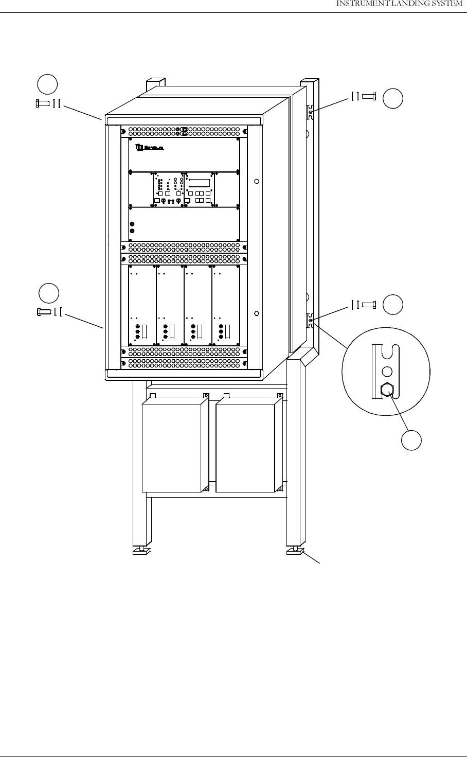
5 Mechanical Installation
The NM70XX cabinet is constructed for mounting on a wall. For easy operation, the keyboard/
display section should be in eye/shoulder height (140-160cm). The RF connectors may be
mounted either on the cabinet top or the cabinet bottom. The free space required around the
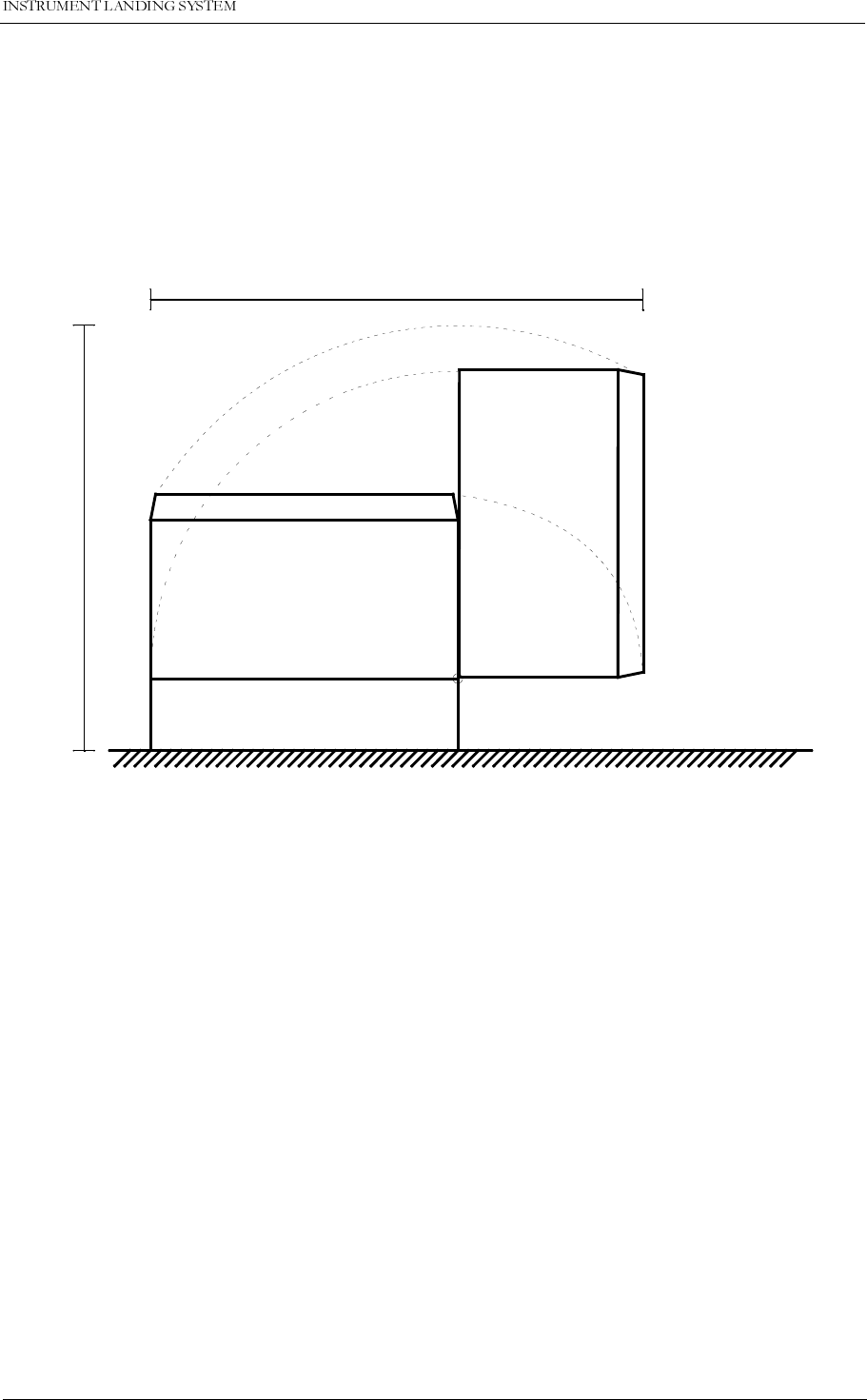
cabinet is approximately one by one meter, see Figure 5-1
Figure 5-1 NM 70XX required mounting space (top view).
5.1 Mounting Kit MK1343A
If the wall is not able to carry the weight of the cabinet (see technical specifications), Navia
Aviation supplies a wall mounting kit, MK1343A. This kit is dimensioned for standard 60 cm
space between studs. For easy mounting, place the cabinet on the rest screws (B) before
entering the mounting screws (A). This is shown in the enlarged view in Figure 5-2
0.9m
1.0m
HBK594-2
1250$5&7(&+1,&$/+$1'%22.
0(&+$1,&$/,167$//$7,21 1DYLD$YLDWLRQ$6
Figure 5-2 NM 70XX mounted on wall with MK1343A.
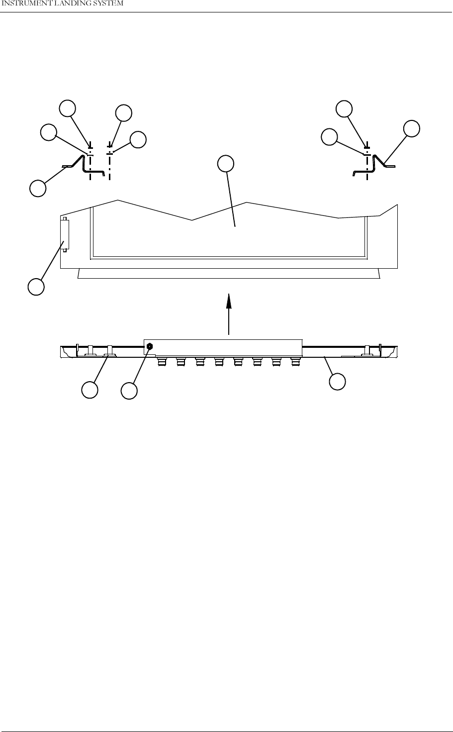
5.2 Moving RF Connectors
If desired the RF connectors may be moved from the cabinet top to the bottom or vice versa,
as illustrated in Figure 5-3. The back section (F) of the main cabinet consists of a connector
plate and a blind plate that are interchangeable. These plates are identical, except for the con-
nectors.
To interchange the plates, follow these instructions:
• Release the nuts (A), washers (B) and flanges (C) on the plates.
• Release the ground connections (D) on the connector plate and (H) on the blind plate.
POWER POWER
Adjustment screw
11
Flat washer M8
Split lock washer M8
Screw M8x25
B
A
A
A
A
HBK597-1
0(&+$1,&$/,167$//$7,21
1250$5&
1DYLD$YLDWLRQ$6
7(&+1,&$/+$1'%22.
• Interchange the plates.
• Remount the nuts, washers and flanges in the order shown.
• Remount the ground connections (D) and (H). Make sure they are located on the hinge (G)
side of the cabinet.
Figure 5-3 Moving the RF connectors to the cabinet bottom.
CL
D
NF
C
A
B
A
B
CSB CLRCLR DS SBO CLR
E
SBO CSB
A
F
BC
G
H
HBK596-1

(/(&75,&$/,167$//$7,21
1250$5&
1DYLD$YLDWLRQ$6
7(&+1,&$/+$1'%22.
6 Electrical Installation
This paragraph describes the external electrical connections of the NM 7033 main cabinet.
6.1 Connection Overview
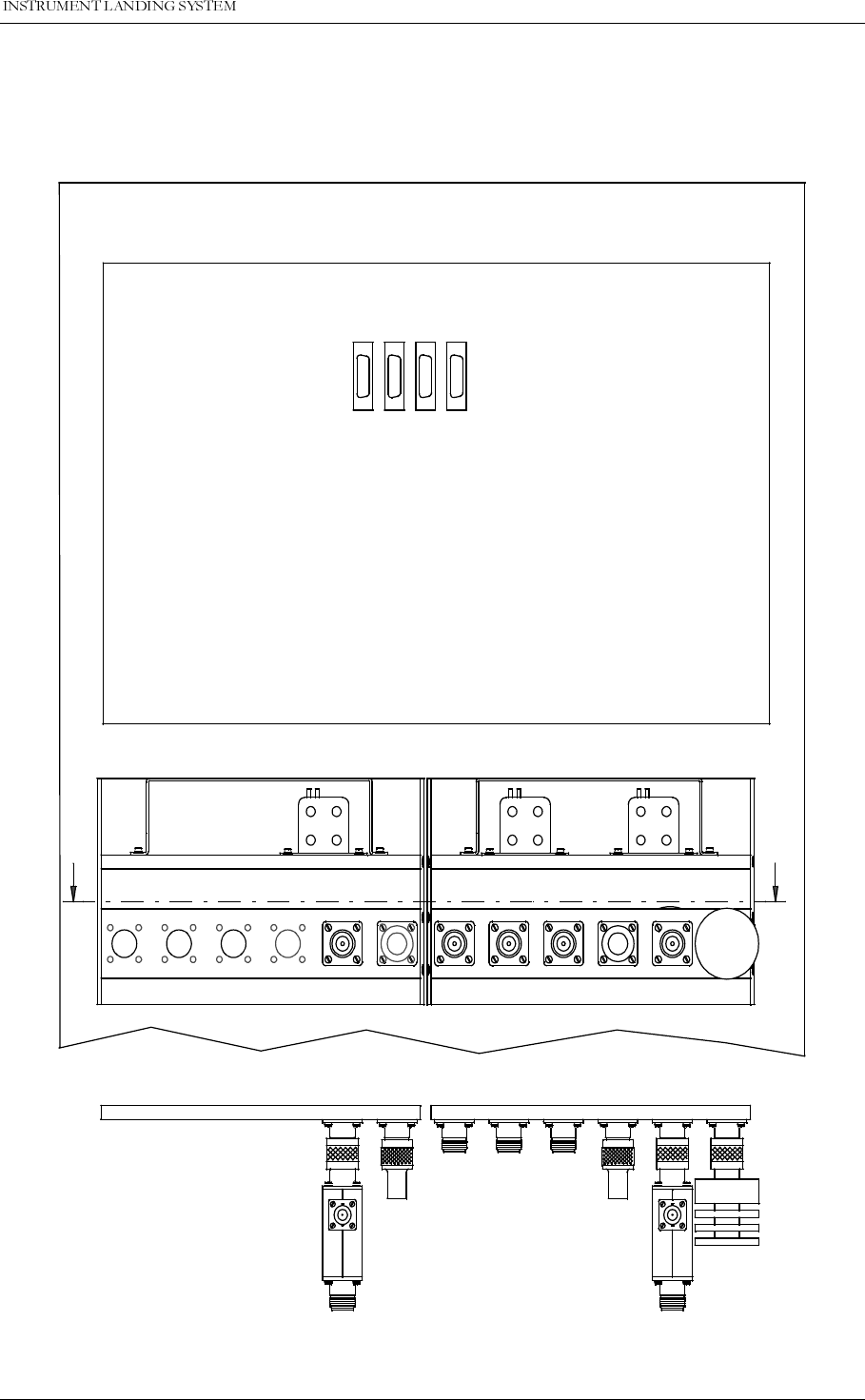
The ILS main cabinet consists of three connector sites, illustrated in Figure 6-1
• The ILS RF signals to and from the antenna system are connected at the top of the main
cabinet. These connectors may be moved to the bottom, see
Mechanical Installation
.
• The power supply (supplies) and the backup battery are connected to the power connector
rail inside the cabinet back section.
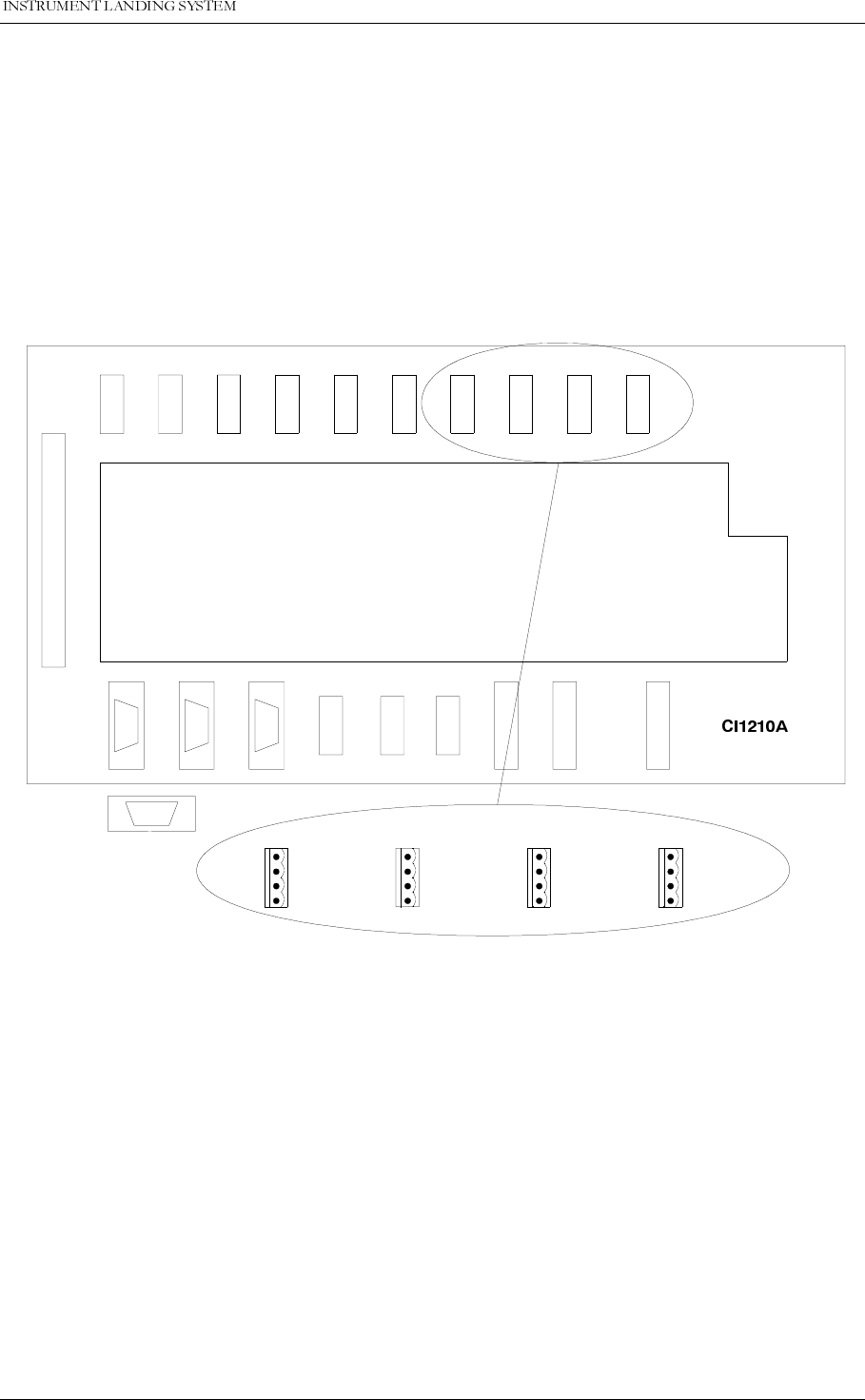
• All other external connections are sited on the Connection Interface board CI1210A inside
the cabinet back section.
Figure 6-1 ILS main cabinet connection overview.
6.2 Power and Battery
The power supply and the backup battery are connected to the power connector rail inside the
cabinet back section as shown in Figure 6-2. If two power supplies are used, these are parallel
RF CONNECTIONS
CABLE FEEDTHROUGH
COU/SBO
CLR/SBO
CLR/CSB
OUT
COU/CSB
CLR
DS
NF
IN CL
1 AC LEVEL MEASUREMENT
CI 1210A CONNECTIONS
8 DIGITAL INPUT/OUTPUT
3 DIFFERENTIAL ANALOG
2 TEMP SENSORS
1 DME
1 REMOTE CONTROL
3 RS 232
4 DC LOOPS
BATTERY +27V
0V
POWER RAIL CONNECTIONS
SUPPLY
POWER +27V
0V
HBK574-2
1250$5&7(&+1,&$/+$1'%22.
(/(&75,&$/,167$//$7,21 1DYLD$YLDWLRQ$6
coupled outside the cabinet. The cables used should have 4mm2 intersection.
Figure 6-2 Power and backup battery connections.
A DC powered modem or other external equipment designed for 22V - 27V DC can be con-
nected to the fused terminal block marked Modem. Maximum current consumption should be
1 A.
6.3 RF Inputs
The RF inputs are:
• Course Line - CL.
• Near Field Antenna - NF.
• Displacement Sensitivity - DS.
• Clearance - CLR (two frequency applications only).
Battery
0V +27V
Power Supply
0V +27V
HBK576-2
(/(&75,&$/,167$//$7,21
1250$5&
1DYLD$YLDWLRQ$6
7(&+1,&$/+$1'%22.
These are connected as shown in Figure 6-3 (front view).
Figure 6-3 RF input connections.
6.4 RF Outputs
The RF outputs are sited at the cabinet top as illustrated in Figure 6-4. The connections are:
All applications:
• COU SBO - COUrse Tx SideBand Only.
• COU CSB - COUrse Tx Carrier and SideBand.
Two frequency applications:
• CLR SBO - CLeaRance Tx SideBand Only.
• CLR CSB - CLeaRance Tx Carrier and SideBand
.
Figure 6-4 RF output connections.
NF CL CLR DS
HBK577-2
COU
CSB
COU
SBO
CLR
CSB
CLR
SBO
HBK578-2
1250$5&7(&+1,&$/+$1'%22.
(/(&75,&$/,167$//$7,21 1DYLD$YLDWLRQ$6
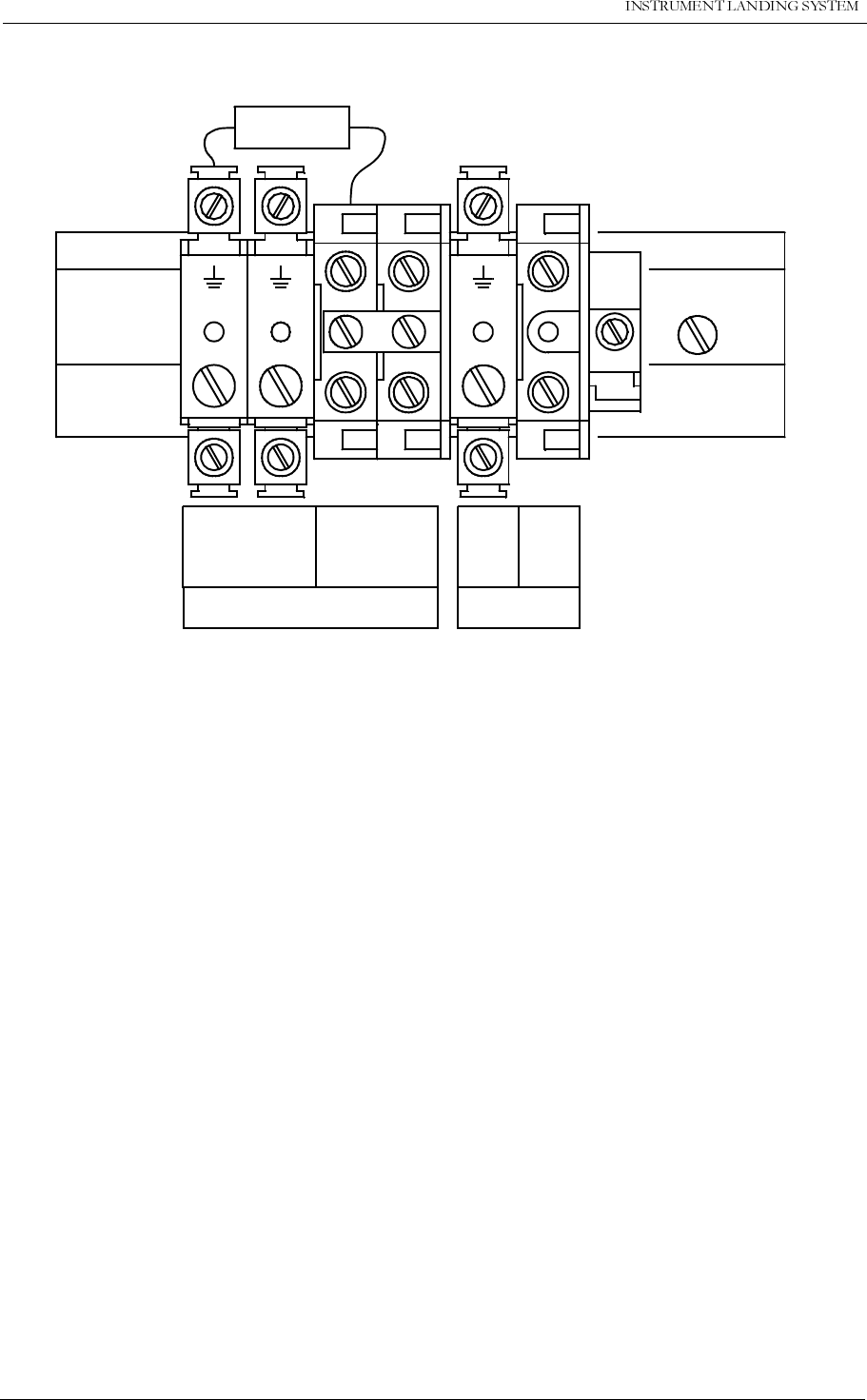
6.5 DC Loop (Localizer only)
The DC loops are connected to the Connection Interface board CI1210A in the cabinet back
section. Location and pin out are illustrated in Figure 6-5
•
DL_REF*
are the reference voltages from the main cabinet.
•
DL_DETECT*
are the return voltages from the antennas.
•
GND
is main cabinet ground.
Suitable female connectors are Weidemüller
BLZ-5.08/6
or equivalent.
Figure 6-5 DC loop connections.
TEMP
INDOOR TEMP
OUTDOOR AC
LEVEL ANALOG
CH.1 ANALOG
CH.2 ANALOG
CH.3 DIGITAL
PORT A DIGITAL
PORT B DIGITAL
PORT C DIGITAL
PORT D
TO MB1203
RS232 RS232 RS232 REMOTE
CONTROL
DC-LOOP DC-LOOP DME
LOCAL REMOTE 2 REMOTE 1 CH.1&2 CH.3&4
1
6
DC-LOOP
CH.1&2
DC-LOOP
CH.3&4
1 - Ch 1 In
2 - Ch 1 Out
3 - GND
4 - Ch 2 In
5 - Ch 2 Out
6 - GND
CI 1210A
1 - Ch 3 In
2 - Ch 3 Out
3 - GND
4 - Ch 4 In
5 - Ch 4 Out
6 - GND
1
6
BATTERY
WARNING
HBK579-2
RADIO LINK
(/(&75,&$/,167$//$7,21
1250$5&
1DYLD$YLDWLRQ$6
7(&+1,&$/+$1'%22.
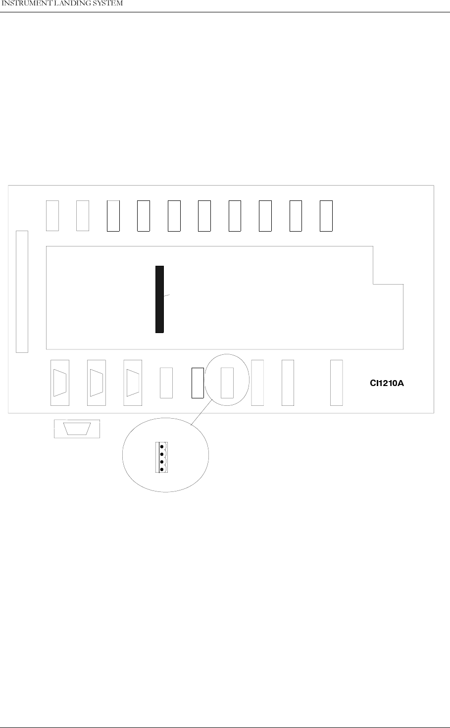
6.6 Remote Control
The remote control is connected to the Connection Interface board CI1210A as illustrated in
Figure 6-6. The connection of the remote control, remote slave panel and interlock switch is
done at the remote control site and covered in chapter 6.13 - 6.16
•
FSK_[P,N]
is the modem line pair.
•
GND
is main cabinet ground.
For normal FSK modem operation the straps S9-11 on CI1210A should be mounted.
A suitable female connector is Weidemüller
BLZ-5.08/4
or equivalent.
Figure 6-6 Remote control connection.
TEMP
INDOOR TEMP
OUTDOOR AC
LEVEL ANALOG
CH.1 ANALOG
CH.2 ANALOG
CH.3 DIGITAL
PORT A DIGITAL
PORT B DIGITAL
PORT C DIGITAL
PORT D
TO MB1203
RS232 RS232 RS232 REMOTE
CONTROL
DC-LOOP DC-LOOP DME
LOCAL REMOTE 2 REMOTE 1 CH.1&2 CH.3&4
REMOTE
CONTROL
1 - GND
2 - FSK_P
3 - FSK_N
4 - GND
1
4
S9-14
BATTERY
WARNING
HBK580-1
RADIO LINK
1250$5&7(&+1,&$/+$1'%22.
(/(&75,&$/,167$//$7,21 1DYLD$YLDWLRQ$6
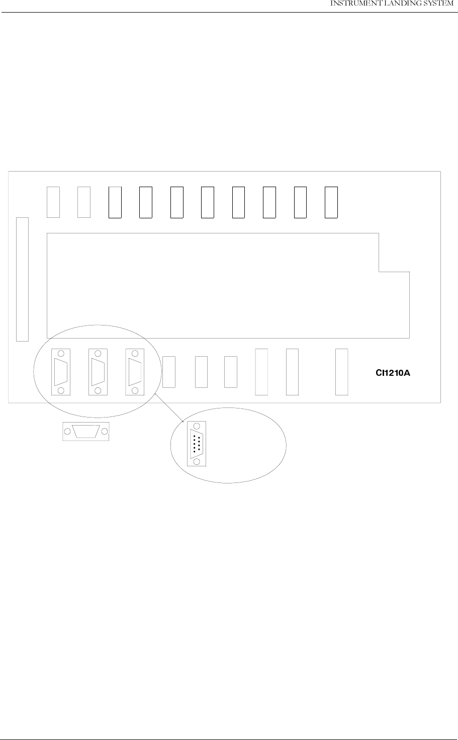
6.7 PC and Modem
PC terminals and modems are connected to the standard pin out RS232, 9 pins DSUB con-
nectors on the Connection Interface board CI1210A as illustrated in Figure 6-7
Recommended connections are:
• LOCAL - the PC located at the ILS main cabinet site.
• REMOTE 1 - the PC located at the airport technical maintenance site.
• REMOTE 2 - distant PC terminals connected through a modem.
Figure 6-7 PC and modem connections.
TEMP
INDOOR TEMP
OUTDOOR AC
LEVEL ANALOG
CH.1 ANALOG
CH.2 ANALOG
CH.3 DIGITAL
PORT A DIGITAL
PORT B DIGITAL
PORT C DIGITAL
PORT D
TO MB1203
RS232 RS232 RS232 REMOTE
CONTROL
DC-LOOP DC-LOOP DME
LOCAL REMOTE 2 REMOTE 1 CH.1&2 CH.3&4
1
5
6
9
1 - CD (REMOTE 2 only)
2 - RXD
3 - TXD
4 - DTR (REMOTE 2 only)
5 - GND
6 - DSR (REMOTE 2 only)
7 - RTS
8 - CTS
9 - Not connected
BATTERY
WARNING
HBK581-1
RADIO LINK
(/(&75,&$/,167$//$7,21
1250$5&
1DYLD$YLDWLRQ$6
7(&+1,&$/+$1'%22.
6.8 DME (localizer only)
Distance Measurement Equipment DME is connected to the Connection Interface board
CI1210A as illustrated in Figure 6-8
•
ACT_DME[P,N]
is the positive and negative terminal of the DME active signal from the
DME, respectively.
•
IN_DME[P,N]
is the positive and negative terminal of the morse code envelope signal from
the DME, respectively.
•
OUT_DME[P,N]
is the positive and negative terminal of the morse code envelope signal to
the DME, respectively.
A suitable female connector is Weidemüller
BLZ-5.08/6
or equivalent.
Figure 6-8 DME connections.
TEMP
INDOOR
TEMP
OUTDOOR
AC
LEVEL
ANALOG
CH.1
ANALOG
CH.2
ANALOG
CH.3
DIGITAL
PORT A
DIGITAL
PORT B
DIGITAL
PORT C
DIGITAL
PORT D
TO MB1203
RS232 RS232 RS232 REMOTE
CONTROL
DC-LOOP DC-LOOP DME
LOCAL REMOTE 2 REMOTE 1 CH.1&2 CH.3&4
1 - ACT_DMEP
2 - ACT_DMEN
3 - IN_DMEP
4 - IN_DMEN
CI1210A
1
6
S1-8
DME
5 - OUT_DMEP
6 - OUT_DMEN
BATTERY
WARNING
HBK582-1
RADIO LINK
1250$5&7(&+1,&$/+$1'%22.
(/(&75,&$/,167$//$7,21 1DYLD$YLDWLRQ$6
Figure 6-9 DME master connections.
If the DME shall be used as ident master, connect as shown in Figure 6-9. In the RMM pro-
gram,
CLR modulation and DME interface
dialogue (see Operators Manual), set DME as
master and DME active signal to OPEN. The LLZ will now transmit the DME dictated morse
code. If the LLZ does not receive any ident signal for approximately 20 seconds, the LLZ will
start to transmit its own programmed morse code. When the DME signal returns, the LLZ will
start to transmit the DME code instantaneously.
Figure 6-10 LLZ master connections.
If the LLZ shall be used as ident master, connect as shown in Figure 6-10 or Figure 6-11. In
HBK770-1
HBK771-1
(/(&75,&$/,167$//$7,21
1250$5&
1DYLD$YLDWLRQ$6
7(&+1,&$/+$1'%22.
the RMM program,
CLR modulation and DME interface
dialogue (see Operating Manual), set
LLZ as master and the DME active signal according to the DME’s manual. When the DME is
active, the LLZ will send every forth ident word to the DME. When the DME is inactive the LLZ
will be keying four out of four words. If the LLZ shall be keying three out of four words whether
the DME is active or not, disconnect the DME ACTIVE wires and program the DME active sig-
nal to OPEN.
6.9 For the Fernau 2020 DME the following connection is recommended
In the RMM program,
CLR modulation and DME interface
dialogue (see Operating Manual),
set LLZ to master and the DME active signal to OPEN.“
Figure 6-11 LLZ Main connections Fernau 2020 DME.
6.10 Analog Inputs
The analog inputs are connected to the Connection Interface board CI1210A as illustrated in
Figure 6-12
The inputs are:
• ANALOG CH.1-3 - three differential DC analog inputs, P is the positive and N is the nega-
tive terminal.
Maximum voltage:
±15V
Input impedance: 10kohms.
• TINDOOR, TOUTDOOR - temperature measurement inputs with interface to an LM35 tem-
perature sensor.
Maximum voltage:
±15V.
1250$5&7(&+1,&$/+$1'%22.
(/(&75,&$/,167$//$7,21 1DYLD$YLDWLRQ$6
Input impedance: 10kohms.
• AC LEVEL - AC level measurement input. Intended for use with a battery eliminator (i.e.
220/9VAC) to monitor the mains voltage.
Maximum voltage: 24Vpp.
Input impedance: 10kohms.
Suitable female connectors are Weidemüller
BLZ-5.08/4
or equivalent.
Figure 6-12 Analog input connections.
TEMP
INDOOR TEMP
OUTDOOR AC
LEVEL ANALOG
CH.1 ANALOG
CH.2 ANALOG
CH.3 DIGITAL
PORT A DIGITAL
PORT B DIGITAL
PORT C DIGITAL
PORT D
TO MB1203
RS232 RS232 RS232 REMOTE
CONTROL
DC-LOOP DC-LOOP DME
LOCAL REMOTE 2 REMOTE 1 CH.1&2 CH.3&4
TEMP
*
1 - VDD
2 - T*DOOR
3 - GND
4 - Not connected
1
4
LM35
Bottom
view
1 - VACP
2 - GND
3 - VACN
4 - Not connected
AC
LEVEL
1 - ANLG*P
2 - GND
3 - ANLG*N
4 - Not connected
ANALOG
CH.*
1
4
1
4
1
4
1
4
1
4
V+
Vtemp
GND
BATTERY
WARNING
HBK583-1
RADIO LINK
(/(&75,&$/,167$//$7,21
1250$5&
1DYLD$YLDWLRQ$6
7(&+1,&$/+$1'%22.
6.11 Digital Inputs and Outputs
Eight bidirectional digital channels (numbered 0-7) are located on the Connection Interface
board CI1210A as illustrated in Figure 6-13
Logic levels: TTL.
Input impedance: 560ohms.
Suitable female connectors are Weidemüller
BLZ-5.08/4
or equivalent.
Figure 6-13 Digital input/output connections.
6.12 Battery Warning
Two inputs for main power supply failure (backup battery active) are sited on the CI1210A
connection interface board as illustrated in Figure 6-14
Logic levels: Normally high 5V or 0V =battery warning.
Input impedance: 10kohms.
Suitable female connectors are Weidemüller
BLZ-5.08/4
or equivalent.
TEMP
INDOOR TEMP
OUTDOOR AC
LEVEL ANALOG
CH.1 ANALOG
CH.2 ANALOG
CH.3 DIGITAL
PORT A DIGITAL
PORT B DIGITAL
PORT C DIGITAL
PORT D
TO MB1203
RS232 RS232 RS232 REMOTE
CONTROL
DC-LOOP DC-LOOP DME
LOCAL REMOTE 2 REMOTE 1 CH.1&2 CH.3&4
1 - USER_DIG5
2 - GND
3 - USER_DIG4
4 - GND
1
4
1
4
1
4
1
4
DIGITAL
PORT C
1 - USER_DIG3
2 - GND
3 - USER_DIG2
4 - GND
DIGITAL
PORT B
1 - USER_DIG1
2 - GND
3 - USER_DIG0
4 - GND
DIGITAL
PORT A
1 - USER_DIG7
2 - GND
3 - USER_DIG6
4 - GND
DIGITAL
PORT D
BATTERY
WARNING
HBK575-1
RADIO LINK
1250$5&7(&+1,&$/+$1'%22.
(/(&75,&$/,167$//$7,21 1DYLD$YLDWLRQ$6
Figure 6-14 Battery warning connections.
6.13 Remote control connections
The remote control is connected to the corresponding ILS by connecting the REMOTE CON-
TROL connector on Connection Interface CI1210 to P9 on Motherboard MB1346, as shown in
Figure 6-15.
Suitable female connectors are Weidemüller
BLZ-5.08/4
or equivalent. 600 ohms cable
should be used.
TEMP
INDOOR TEMP
OUTDOOR AC
LEVEL ANALOG
CH.1 ANALOG
CH.2 ANALOG
CH.3 DIGITAL
PORT A DIGITAL
PORT B DIGITAL
PORT C DIGITAL
PORT D
TO MB1203
RS232 RS232 RS232 REMOTE
CONTROL
DC-LOOP DC-LOOP DME
LOCAL REMOTE 2 REMOTE 1 CH.1&2 CH.3&4
BATTERY
WARNING
1 - BATT.WARN. CHARGER 1
2 - GND
3 - BATT.WARN. CHARGER 2
4 - GND
CI 1210A
1
4
BATTERY
WARNING
HBK602-2
RADIO LINK
(/(&75,&$/,167$//$7,21
1250$5&
1DYLD$YLDWLRQ$6
7(&+1,&$/+$1'%22.
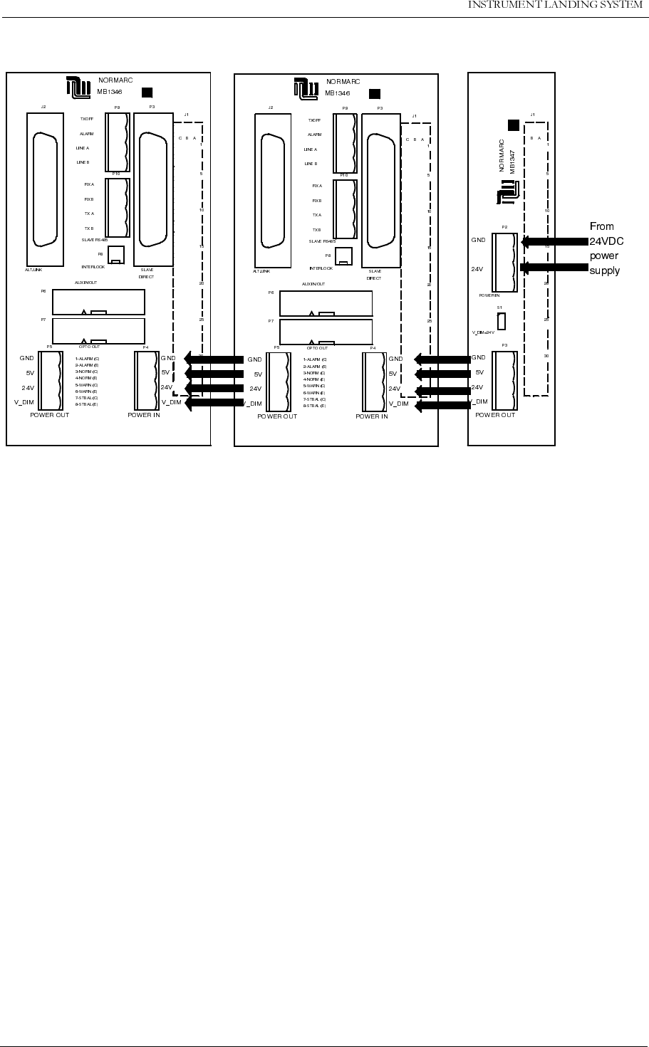
Figure 6-15 Remote control to ILS connection
The power supply to the remote control is connected according to Figure 6-16. The battery
charger is connected to P2 on the MB1347 - power supply motherboard. Output connector P3
on MB1347 is connected to input connector P4 on MB1346 - remote control motherboard.
Several MB1346’s are serial linked by connecting P5 on one board to P4 on the next.
Suitable female connectors are Weidemüller
BLZ-5.08/4
or equivalent.
REMOTE
CONTROL
1 - GND
2 - FSK_P
3 - FSK_N
4 - GND
J2 P3
P6
P7
P4
P5
P9
P10
P8
NORMARC
OPTO OUT
2-ALARM (E)
1-ALARM (C)
4-NORM (E)
5-WARN (C)
6-WARN (E)
7-STBAL (C)
8-STBAL (E)
3-NORM (C)
GND
5V
24V
V_DIM
GND
5V
24V
V_DIM
POWER OUT POWER IN
AUX IN/OUT
SLAVE
DIRECT
INTERLOCK
TXOFF
ALARM
LINE A
LINE B
RX A
RX B
TX A
TX B
SLAVE RS485
J1
ABC
1
5
30
20
25
15
10
ALT.LINK
MB1346
P9
1 - TXOFF
2 - ALARM
3 - LINE_A
4 - LINE_B
CI1210
on
corresponding
ILS
or
CI 1376
on
corresponding
Marker Beacon
HBK772-2
1250$5&7(&+1,&$/+$1'%22.
(/(&75,&$/,167$//$7,21 1DYLD$YLDWLRQ$6
Figure 6-16 Remote control power supply connections
6.14 Automatic shutdown of GP
If required, the GP can be configured to shut down automatically when the LLZ is off. Connect
a wire from P9 ALARM on the Motherboard MB 1346A that belongs to the LLZ to P9 TXOFF
on the MB 1346A that belongs to the GP. Refer to Figure 6-17.
HBK773-1
(/(&75,&$/,167$//$7,21
1250$5&
1DYLD$YLDWLRQ$6
7(&+1,&$/+$1'%22.
Figure 6-17 Automatic GP shutdown connection
6.15 Remote slave connection
The remote slave panel SF1344 is connected to the corresponding remote control’s mother-
board by connecting P3 on MB1346 to P1 on SF1344. P10 on MB1346 is not used. See Fig-
ure 6-18.
Suitable connectors are standard 25 pins female DSUB (Harting 0967 025 0442 and 0967 225
4704 or equivalent), connected by a 10 wire 1:1 cable.
J2 P3
P6
P7
P4
P5
P9
P10
P8
NORMARC
OPTO OUT
2-ALARM (E)
1-ALARM (C)
4-NORM (E)
5-WARN (C)
6-WARN (E)
7-STBAL (C)
8-STBAL (E)
3-NORM (C)
GND
5V
24V
V_DIM
GND
5V
24V
V_DIM
POWER OUT POWER IN
AUX IN/OUT
SLAVE
DIRECT
INTERLOCK
TXOFF
ALARM
LINE A
LINE B
SLAVE RS485
J1
ABC
1
5
30
20
25
15
10
ALT.LINK
MB1346
GP LLZ
HBK1100-1
1250$5&7(&+1,&$/+$1'%22.
(/(&75,&$/,167$//$7,21 1DYLD$YLDWLRQ$6
Figure 6-18 Remote slave connection
6.16 Interlock switch connection
The interlock switch is either connected to P8 on MB1346 (remote control motherboard) or to
P2 on SF1344 (remote slave panel), see Figure 6-19.
Figure 6-19 Interlock switch connection
J2 P3
P6
P7
P4
P5
P9
P10
P8
NORMARC
OPTO OUT
2-ALARM (E)
1-ALARM (C)
4-NORM (E)
5-WARN (C)
6-WARN (E)
7-STBAL (C)
8-STBAL (E)
3-NORM (C)
GND
5V
24V
V_DIM
GND
5V
24V
V_DIM
POWER OUT POWER IN
AUX IN/OUT
SLAVE
DIRECT
INTERLOCK
TXOFF
ALARM
LINE A
LINE B
RX A
RX B
TX A
TX B
SLAVE RS485
J1
ABC
1
5
30
20
25
15
10
ALT.LINK
MB1346
To P1
on
SF1344
1
13
14
25
1 - GND
2 - ALARM
3 - WARNING
4 - NORMAL
7 - GND
15 - V24P
19 - ON_OFF
21 - SILENCE
23 - INTERLOCK (if used)
25 - BUZZER
1:1
HBK 774-1
2
1
MB1346 / P8
OR
SF1344 / P2
INTERLOCK
SWITCH
RWYA RWYB
2
1
1
2
1
2
INTERLOCK
GND
1
2
54 21
LLZ runway A
GP runway A
LLZ runway B
GP runway B
HBK775-2


7(676$1'$'-8670(176
1250$5&
1DYLD$YLDWLRQ$6
7(&+1,&$/+$1'%22.
7 Tests and Adjustments
7.1 Configuration Settings
Follow this procedure to set the configurations in the ILS according to the desired system con-
figuration.
7.1.1 ILS Configuration
Set the correct configuration for this ILS according to this table. The Station Control strap plat-
form is located on Transmitter Control Assembly TCA 1218 (Figure 7-1).
Table 7-1 ILS configuration settings.
1 Strap IN NOT interlock
Strap OUT Interlock
2 Strap IN NOT hot standby
Strap OUT Hot standby
3 Strap IN 2 frequency ILS
Strap OUT 1 frequency ILS
4 Strap IN 1 of 2 voting
Strap OUT 2 of 2 voting (default)
5 Strap IN Lost contact with remote control will NOT turn off transmitters.
Strap OUT Lost contact with remote control will turn off transmitters.
(default)
6 Strap IN WRITE DISABLE switch in horizontal position generate service
condition. (default)
Strap OUT WRITE DISABLE switch in horizontal position does not generate
service condition.
7 Strap IN ACCESS grant switch on remote control must be in access grant
position in order to obtain access level 2 or 3 from the RMM sys-
tem. (default)
Strap OUT ACCESS grant switch on remote control is overridden.
8 Strap IN Tells the RMS that this is a GP ILS.
Strap OUT Tells the RMS that this is a LLZ ILS.
9 Strap IN Spare, Not used.
Strap OUT Spare, Not used.
10 Strap IN Spare, Not used.
Strap OUT Spare, Not used.
1250$5&7(&+1,&$/+$1'%22.
7(676$1'$'-8670(176 1DYLD$YLDWLRQ$6
Figure 7-1 Station Control strap platform.
7.1.2 Remote Ports Access Level Configuration
The allowed access levels on REMOTE ports 1 and 2 on the RMS can be configured by set-
ting jumpers S1-S4 on the Transmitter Control Assembly TCA1218A (Figure 7-1) according to
Table 7-1 .
Jumper in means that access level is allowed.
Jumper out means that access level is denied.
Table 7-2 Access level strap settings.
7.1.3 Warning Configuration
Use the RMM Program to configure which warnings shall cause system warning i.e. illuminate
the RC main warning lamp.
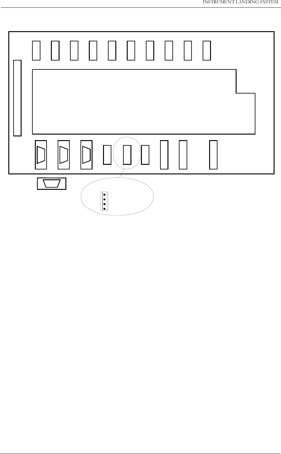
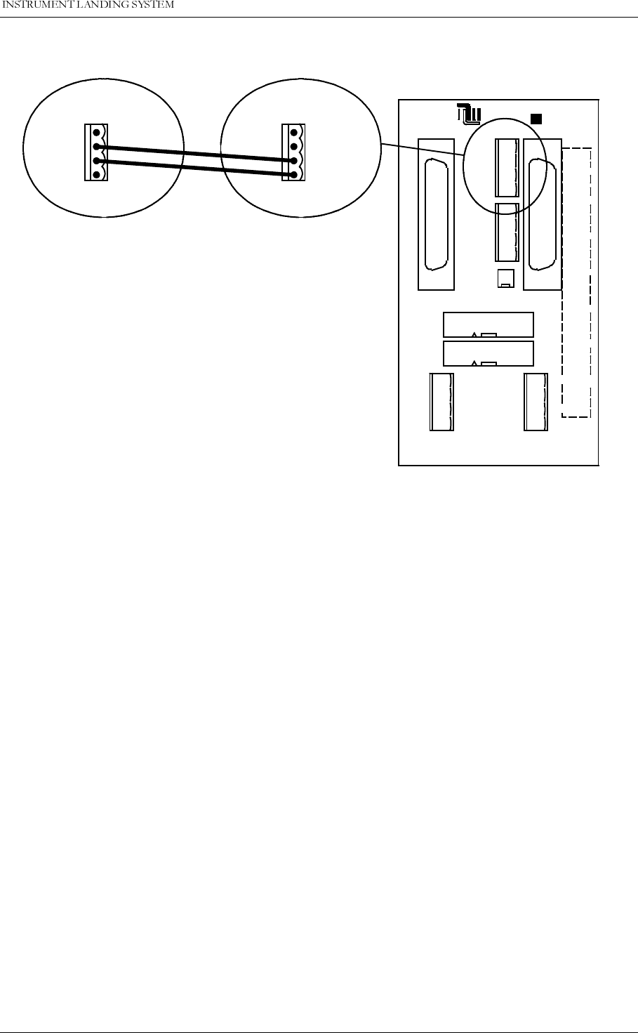
7.1.4 Remote Control Interface (CI 1210)
The transmission medium (telephone line (FSK modem) or RS 232) to the Remote Control
can be selected by plugs and link straps S9 - S14 on the Connection Interface CI 1210 if the
equipment is equipped with the RS-232 cable
Table 7-3 Remote Control Setup
PORT ACC. LEVEL 2 ACC. LEVEL 3
Remote 1 Strap S1 Strap S2
Remote 2 Strap S3 Strap S4
Straps in Function Connector used
S9, S10, S11 Telephone line (FSK
modem) CI 1210, P29
S12, S13, S14* RS-232 9 pin DSUB below CI 1210
1
2
3
4
5
6
7
8
9
10 HBK592-1
7(676$1'$'-8670(176
1250$5&
1DYLD$YLDWLRQ$6
7(&+1,&$/+$1'%22.
* S14 pin 2 connected to ground by plug on cable from P3 pin 20, refer to Figure 7-2
Figure 7-2 Cable connections for Remote Control via RS-232.
7.1.5 Remote Control configuration
The Aural Alarm / Warning functions and transmission medium (telephone line or RS 232) in
the Remote Control can be selected by link straps:
The strap links S6 to S12 will give Aural Warning for the following warning parameters when
connected:
HBK1121-1
1250$5&7(&+1,&$/+$1'%22.
7(676$1'$'-8670(176 1DYLD$YLDWLRQ$6
Table 7-4 Aural warning configuration
Table 7-5 Warning reset (Silence):
Table 7-6 Buzzer:
Table 7-7 Telephone Line / RS 232 / TTL logic:
Strap Warning Parameter
S6 Standby Alarm (Hot Standby racks only)
S7 Parameter Warning
S8 Ident Warning
S9 Battery Warning
S10 Standby on Air
S11 Monitor Disagree Warning
S12 Maintenance Warning
Strap Function
S1 in Silence on Remote Control resets Remote Control buzzer only
S1 out Silence on Remote Control resets both Remote Control and Slave Panel
buzzer
S5 in Silence on Slave Panel resets Slave Panel buzzer only
S5 out Silence on Slave Panel resets both Remote Control and Slave Panel
buzzer
Strap Function
S4 in Buzzer connected
S4 out Buzzer disconnected
S2 pins con-
nected S3 pins con-
nected Function Input used on MB 1346A
1-2 1-2 Telephone line P9 Line A and Line B
3-4 3-4 RS 232 J2 Alt. link
5-6 5-6 TTL logic Not supported
7(676$1'$'-8670(176
1250$5&
1DYLD$YLDWLRQ$6
7(&+1,&$/+$1'%22.
7.2 Technical note - Leased Line Setup for Remote Control (Westermo)
This description applies to Westermo TD-22 GB modems used to connect the remote control
to the ILS rack.
7.2.1 DIP switch settings
SW1:
* For the modem connected to the cabinet use: X = 0 (Answer mode).
For the modem connected to the Remote Control use: X = 1 (Dial mode).
SW2:
SW3:
SW4:
SW5:
7.2.2 Strap settings on modems
The modems needs an active CTS for being able to transmit. Since there are no handshaking
from ILS or RC to modems, the CTS signal must be activated by connecting the modems own
RTS to it’s CTS. This is done by connecting the RTS and CTS together on the screw-block
above the 25-pins D-sub on each modem.
7.2.3 Connecting modem to the cabinet
The modem must be connected to RC RS232 on the connection interface board in the ILS
cabinet. The signals on the 9-pin connector in the cabinet should be connected 1:1 to the 25-
4321
1 0 1 X* Leased line, switch off echo and result code.
All AT commands ignored, including +++
87654321
00001001Enable SW2:2 to 7. Asynchronous. DTR/DSR discon-
nected.
87654321
000000012-wire connection.
87654321
01010001300 baud. 8 data bits, odd parity, 1 stop bit
87654321
00000001V.21 300 bps

1250$5&7(&+1,&$/+$1'%22.
7(676$1'$'-8670(176 1DYLD$YLDWLRQ$6
pins connector on the modem. Normally a 9 to 25-pins converter and a 1:1 flat cable will be
used to connect the modem to the cabinet.
7.2.4 Connecting modem to the RC
The modem must be connected to J2 on MB1346 (remote control motherboard) using 25-pins
D-sub connectors with a 1:1 cable.
7.2.5 Connecting the two modems
Connect the two modems by using the standard Line connection marked TEL LINE on the
modems.
7.3 Transmitter Alignments and Calibration
Test Equipment required:
• Oscilloscope general purpose
• NM 3710 Field Test Set (with 20 dB attenuator)
• BNC Test Cable
• Frequency Counter RF
Carry out the alignment steps in the order outlined below:
7.3.1 RF Phase feedback adjustment
7.3.2 RF power
7.3.3 LF phase adjustment
7.3.4 RF power balance adjustment
7.3.5 RF phase combiner at I/P
7.3.6 SDM calibration
7.3.7 DDM calibration
7.3.7.1 Test DDM setting
7.3.8 Ident tone modulation depth
7.3.9 RF frequency adjustment
NOTE:
If some of the functions/parameters depart considerably from normal, then repeat the steps in
sequence once more, except steps 7.3.7.1 - 7.3.9.
NOTE:
This adjustment procedure assumes that the LPAs and GPAs RF level, DDM and SDM
parameters are correctly adjusted. Site adjustments should be limited to small touch up
adjustments on RF phase, RF phase feedback and RF power balance. If RF power balance is
adjusted, the resulting DDM change should be compensated with the 90Hz and 150Hz poten-
tiometers at the back of the LPA / GPA.
7.3.1 RF Phase Feedback Adjustment
Connect the oscilloscope to the BNC test connector labelled PHASE CORR. located on the
transmitter modules.
NOTE
7(676$1'$'-8670(176
1250$5&
1DYLD$YLDWLRQ$6
7(&+1,&$/+$1'%22.
Set the scope’s input mode to DC.
The waveform observed should take a continuous form without limiting segments or deep
notches or other discontinuities.
(Each modulator develops it’s own waveform shape due to spreads in insertion phases).
The dynamic maximum point should be adjusted to approximately -4 volt.
The average operating point of the PHASE CORR signal can be shifted by means of adjusting
potentiometer PH.OFFS. at the back of the LPA/GPA.
7.3.2 RF Power
The CSB and corresponding SBO output power can be adjusted by means of the RMM Pro-
gram or the Local Display/Keyboard.
Table 7-8 Normal operating power level
The output power can be read by means of the RMM Program or the Local Display/Keyboard.
7.3.3 LF Phase Adjustment
Figure 7-3 LF phase CSB illustration.
LLZ Course 15W CSB
LLZ Clearance 15W CSB
GP Course 5W CSB
GP Clearance 0,5W CSB
DEMODULATION CSB: NORMAL DEMODULATION CSB 10° LF PHASE ERROR

1250$5&7(&+1,&$/+$1'%22.
7(676$1'$'-8670(176 1DYLD$YLDWLRQ$6
Figure 7-4 LF phase SBO illustration.
7.3.3.1 One-frequency system
Connect oscilloscope channel A to the BNC test connector labelled CSB located on LPA/GPA
Course 1 (2).
Set oscilloscope input mode to DC.
Adjust 150 Hz COU phase adj R3 on Low Frequency generator LF1223A (Figure 7-9)
observing oscilloscope channel A until the waveform equals left hand graph in Figure 7-2.
A significant indication of correct LF phase is that the pair of the intermediate peaks are equal
in amplitude.
7.3.3.2 Two-frequency system
Connect oscilloscope channel A to the BNC test connector labelled CSB located on LPA/GPA
Course 1 (2).
Connect oscilloscope channel B to the BNC test connector labelled CSB located on LPA/GPA
Clearance 1 (2).
Set oscilloscope input mode to DC. Select CHOP mode.
Adjust channel A and B gain so that both waveforms show the same amplitude.
By means of the RMM turn off 90 Hz modulation for Course Tx and Clearance Tx.
On Low Frequency generator LF1223A Tx1 (Tx2) adjust 150 Hz COU phase adj. R3 to phys-
ical centre position.
Adjust 150 Hz CLR phase adj. R180 to track 150 Hz Course waveform in the same phase
(waveform overlap).
By means of the RMM turn on 90 Hz modulation for both Course Tx and Clearance Tx.
Adjust 90 Hz COU phase adj. R1 (LF1223A) observing oscilloscope channel A until the
waveform equals left hand graph in Figure 7-2.
DEMODULATION SBO: NORMAL DEMODULATION SBO 10° LF PHASE ERROR
7(676$1'$'-8670(176
1250$5&
1DYLD$YLDWLRQ$6
7(&+1,&$/+$1'%22.
Adjust 90 Hz CLR phase adj. R179 (LF1223A) observing oscilloscope channel B until the
waveform equals left hand graph in Figure 7-2.
A significant indication of correct LF phase is that the pair of the intermediate peaks are equal
in amplitude.
7.3.4 RF Power Balance Adjustment
Connect the oscilloscope to the BNC test connector labelled SBO located on the transmitter
modules.
NOTE:
Set the scope’s input mode to DC.
Figure 7-5 Power balance SBO illustration.
Perfect power balance between the 90 Hz modulated carrier and the 150 Hz modulated car-
rier is indicated when the two largest sets of peak waveforms fall on lines parallel to the base-
line.A more accurate way of observing a power balance error is to double the sweep rate in
non-trigger mode such that the second 60 Hz half of the cycle is folded back on the first half
and tracks the envelope waveform.
RF Power Balance can be adjusted by potentiometer RF-BAL on the back of the LPA/GPA.
Adjust until both halves fall on the same envelope waveform or the two largest sets of peak
waveforms fall on lines parallel to the baseline.
NOTE:
Changes in DDM as a result of RF power balance adjustment should be compensated with
the 90Hz and 150Hz potentiometers at the back of the LPA / GPA.
7.3.5 RF Phase at Combiner I/P
Connect the oscilloscope to the BNC test connector labelled SBO located on the transmitter
modules.
NOTE:
Set the scope’s input mode to DC. Set the oscilloscope in normal trigger mode such that the
waveform below can be observed.
DEMODULATION SBO: 1dB POWER
IMBALANCE (150Hz<90Hz)
DEMODULATION SBO: NORMAL

1250$5&7(&+1,&$/+$1'%22.
7(676$1'$'-8670(176 1DYLD$YLDWLRQ$6
.
Figure 7-6 RF phase SBO illustration
The RF phase (90° start phase) can be adjusted by trimmer RF PHASE on the back of the
LPA/GPA. Adjust until the minima points between the smallest peak waveform reach the base-
line or a minimum.
7.3.6 SDM Calibration
Connect the NM 3710 Field Test Set to the CSB BNC test connector in the Cabinet's Change-
over section.
(Insert a 20 dB attenuator at the input of the Field Test Set in order to avoid overloading).
SDM should be calibrated to 80,0% +/- 0,1% SDM by adjusting SDM from the RMM Program
or the Local Display/Keyboard.
7.3.7 DDM Calibration
NOTE:
Check that all TEST DDM settings are in NORMAL.
Connect the NM 3710 Field Test Set to the CSB BNC test connector in the Cabinet's Change-
over section.
(Insert a 20 dB attenuator at the input of the Field Test Set in order to avoid overloading).
DDM should be calibrated to 0.0% +/-0.05% DDM by adjusting DDM from the RMM Program
or the Local Display/Keyboard.
7.3.7.1 Test DDM Setting
TEST DDM with 90Hz or 150Hz dominance can be switched on and off from the RMM Pro-
gram or the Local Display/Keyboard. The DDM values inserted by TEST DDM are preset val-
ues which is set as described below.
90Hz Dominance Preset
Utilize the Field Test Set as in the previous test.Set the TEST DDM in position 90 Hz domi-
nance from the RMM Program or the Local Display/Keyboard. Adjust the (90 Hz) test DDM
setting until a wanted DDM value indicating (-) sign is obtained. (Typical value: -0.8%...-1.0%
DEMODULATION SBO: 5° RF PHASE ERRORDEMODULATION SBO: NORMAL

7(676$1'$'-8670(176
1250$5&
1DYLD$YLDWLRQ$6
7(&+1,&$/+$1'%22.
DDM).
150Hz Dominance Preset
Utilize the Field Test Set as in the previous test.Set the TEST DDM in position 150 Hz domi-
nance from the RMM Program or the Local Display/Keyboard. Adjust the (150 Hz) test DDM
setting until a wanted DDM value indicating (+) sign is obtained. (Typical value: 0.8%...1.0%
DDM).
Set the TEST DDM back to normal.
7.3.8 Ident Tone Modulation Depth
7.3.8.1 Method 1
Connect the Field Test Set to the CSB BNC test connector in the Cabinet’s Change-over sec-
tion.
(Insert a 20 dB attenuator at the input of the Field Test Set in order to avoid overloading).
Set the Ident Control to CONTINUOUS from the RMM Program or the Local Display/Key-
board.
On the Field Test Set, press IDENT.
1020 Hz modulation depth can be adjusted from the RMM Program or the Local Display/Key-
board.
Adjust modulation depth to 10.0% +/-0.3%.
If VOICE modulation is implemented, the ident modulation depth should be set to 5.5% +/-
0.3% to avoid over modulation. Before this adjustment is done, follow the instructions in the
appendix VOICE GENERATOR. Make sure VOICE is turned off from the RMM program or the
Local Keyboard/Display when adjusting the modulation depth.
7.3.8.2 Method 2
An alternative method of checking 1020 Hz modulation depth to 10% is described below:
Connect the oscilloscope to the BNC test Connector labelled CSB.
Switch off the 90 Hz modulation and the 1020 Hz modulation.
Note the peak-to-peak deflection of the remaining 150 Hz waveform.
Then switch off the 150 Hz modulation and switch the 1020 Hz modulation to CONTINUOUS.
The observed 1020 Hz peak-to-peak waveform amplitude should be 50% of the 150 Hz ampli-
tude providing the 1020 Hz modulation depth is 10% (or 1/2 of 150 Hz depth).
7.3.9 RF Frequency Adjustment
Fine-adjustment of the operating frequency can be carried out by adjusting C1 in the
OS1221A/B RF Oscillator module.

1250$5&7(&+1,&$/+$1'%22.
7(676$1'$'-8670(176 1DYLD$YLDWLRQ$6
The top cover must be removed.
Mount the Oscillator OS1221A/B on an extension board.
In order to monitor the frequency, connect the Frequency Counter to the BNC test connector
labelled CSB. (Make sure the transmitter under test is routed to Antenna). If necessary for sta-
ble counting switch off modulation tones.
Adjust until frequency is less than 1 kHz from operating frequency. Trimmer C1 adjusts course
and clearance frequencies simultaneously.
7.4 Antenna System Adjustments
After the transmitters has been aligned correctly the antenna system must be aligned. This
includes mechanical adjustments of the Antenna System, electrical adjustments (phasing)
and adjustments of the ADU and MCU.
For details, refer to the adjustment procedure for each antenna system.
7.5 Monitor Alignment and Calibration.
Test Equipment required:
• Oscilloscope, general purpose
• NM 3710 Field Test Set (with 20 dB attenuator)
• BNC Test Cable
• Digital Voltmeter, 4 digits, DC
7.5.1 General
Description is given only for the DS channels. R338++ means that the other channels has
numbers R1338, R2338 and R3338 for CL, CLR and NF channels.
Before any monitor adjustments are attempted, the following procedures shall be completed:
Transmitter calibrations
Network alignments
It is imperative for the result that the signals from the Monitor Combining Network (MCU) are
correct. Check these signals with the NM3710, Field Test Set,
These signals are used for aligning the monitors.
7.5.2 RF Input Level Adjustment.
Mount the Monitor Frontend MF12xx on an extender card.
Turn on the transmitters.
7(676$1'$'-8670(176
1250$5&
1DYLD$YLDWLRQ$6
7(&+1,&$/+$1'%22.
Set the potentiometer R338++ in middle position. See Figure 7-7.
Figure 7-7 Adjustment points on Monitor Frontend MF12xx.
Adjust the jumper settings in P2++ and potentiometer R338++ until the voltage is 240mV at
TP23++.
Figure 7-8 Alternative jumper settings of P2++
Turn off the equipment and remove the extender card. Set the Monitor Frontend MF12xx in its
correct position. Turn on the transmitters.
Adjust the RF level potentiometer on the front of Monitor Frontend MF12xx until the monitor
gives a RF level reading of 3.0V.
7.5.3 AGC Time Adjustment
Turn on the transmitters.
Make a note of the AGC voltages on TP 1,2,3 and 4 on MF12xx.
Turn off the transmitters.
Adjust the AGC TIM potentiometer on the front of Monitor Frontend MF12xx until the AGC
voltage (TP1,2,3 or 4) is the same as with a nominal RF input.
HBK776-2
HBK777-2

1250$5&7(&+1,&$/+$1'%22.
7(676$1'$'-8670(176 1DYLD$YLDWLRQ$6
Do this for all four monitor channels on all of the Monitor Frontend MF12xx modules in the
system.
This ensures fast response from the monitors.
7.5.4 SDM Adjustment
Adjust the SDM potentiometer on the front of Monitor Frontend MF12xx until the monitors
reads 40.0/80.0%SDM +/- 0.1%SDM.
7.5.5 DDM Adjustment
Measure and note down the DDM values from the MCU and NF antenna with help of the Field
Test Set.
Set the Nominal values for each channel to the measured values with help of the RMM Pro-
gram.
7.6 Monitor Alarm Setting Procedure
Type in the wanted alarm limits from the RMM Program or the Local Display/Keyboard.
The monitors will have preset alarm limits when the ILS is delivered for factory.
These alarm limits are as listed in the table below:
Table 7-9 Localizer alarm limits.
* Only for single frequency ILS. For two frequency ILS the limit is +/- 1dB.
CL DS NF CLR
LLZ CAT1 DDM 15uA 25uA 15uA 40uA
SDM ± 4% ------ ------ ± 4%
RF level ± 3dB* ------ ------ ± 1dB
CAT II DDM 11uA 15uA 11uA 40uA
SDM ± 4% ------ ------ ± 4%
RF level ± 3dB* ------ ------ ± 1dB
CATIII DDM 9uA 15uA 9uA 40uA
SDM ± 4% ------ ------ ± 4%
RF level ± 3dB* ------ ------ ± 1dB

7(676$1'$'-8670(176
1250$5&
1DYLD$YLDWLRQ$6
7(&+1,&$/+$1'%22.
Table 7-10 Glidepath alarm limits
* Only for single frequency ILS. For two frequency ILS the limit is +/- 1dB.
CLR transmitter is only present in two frequency ILS.
7.7 Maintenance Limit Adjustments
Use the RMM Program to set maintenance warning limits in the system. All new systems will
have factory preset maintenance warning limits. Maintenance warning limits can not be set
from the Local Display/Keyboard.
CL DS NF CLR
GP CAT1 DDM 30uA 37uA 30uA 45uA
SDM ± 5% ------ ------ ± 5%
RF level ± 3dB* ------ ------ ± 1dB
CAT II DDM 30uA 37uA 30uA 45uA
SDM ± 5% ------ ------ ± 5%
RF level ± 3dB* ------ ------ ± 1dB
CATIII DDM 30uA 37uA 30uA 45uA
SDM ± 5% ------ ------ ± 5%
RF level ± 3dB* ------ ------ ± 1dB
1250$5&7(&+1,&$/+$1'%22.
7(676$1'$'-8670(176 1DYLD$YLDWLRQ$6
7.8 Adjustment points
Figure 7-9 Front side adjustment points.
11
LF 1223A
MF 1211A
ESC PREV NEXT
-+
ENTER
READ
QUICK
CLR
COAXIAL
COURSE
MAIN
POSITION
WRITE
PROTECT
WARNING
ON/
NORMAL
INTERLOCK
OVERRIDE
MAINT
STBY
OFF
REMOTE
LOCAL
AUTO
MANUAL
OVER
CHANGE TX1
ALARM
SERVICEPARAM
DISAGR
BATT
IDENT
TX1
TX2
TX2
STAND
BY
Mon.1 Mon.2 Mon.stby.
90Hz COU phase adj.
150Hz COU phase adj.
90Hz CLR phase adj.
150Hz CLR phase adj.
TX1 TX2
NF SDM adj.
NF AGC time constant adj.
NF RF level adj.
CL SDM adj.
CL AGC time constant adj.
CL RF level adj.
CLR SDM adj.
CLR AGC time constant adj.
CLR RF level adj.
DS SDM adj.
DS AGC time constant adj.
DS RF level adj.
Ident mod adj.
HBK698-2

7(676$1'$'-8670(176
1250$5&
1DYLD$YLDWLRQ$6
7(&+1,&$/+$1'%22.
Figure 7-10 CI1210A Connection Interface adjustment point.
TEMP
INDOOR TEMP
OUTDOOR AC
LEVEL ANALOG
CH.1 ANALOG
CH.2 ANALOG
CH.3 DIGITAL
PORT A DIGITAL
PORT B DIGITAL
PORT C DIGITAL
PORT D
TO MB1203
RS232 RS232 RS232 REMOTE
CONTROL
DC-LOOP DC-LOOP DME
LOCAL REMOTE 2 REMOTE 1 CH.1&2 CH.3&4
BATTERY
WARNING
Battery protection
level adj.
HBK697-1

)81&7,21$/'(6&5,37,21
1250$5&
1DYLD$YLDWLRQ$6
7(&+1,&$/+$1'%22.
3$57,,,'(6&5,37,21
8 Functional Description
8.1 Introduction
The NM 7000-series Instrument Landing System is a fourth generation system featuring
extensive remote maintenance and monitoring features and systematic use of modern elec-
tronic components and processors.
Careful analysis has guided the partitioning of the system into analog hardware, digital hard-
ware and software to meet the reliability and integrity objectives as well as easy maintenance
and low cost of ownership.
In the monitor, comparison between monitor measurements and stored monitor limits is per-
formed by digital hardware. Thus safety critical software is avoided in those functions. The fil-
tering functions are performed by a dedicated signal processor running a FFT algorithm, with
the signals sampled after base-band detection.
The transmitter/modulator uses a synthesizer as a RF source. In two-frequency systems a
common reference crystal is used, avoiding drift in difference frequency. The LF and ident fre-
quencies and ident keying are generated by digital hardware, while the level setting and mod-
ulation control are performed by digitally controlled analog feedback loops.
Local and remote control, and change-over and shut-down functions are performed by digital
hardware.
Software is used for the remote maintenance and monitoring functions, including alarm and
parameter storage, diagnostic functions, transmitter adjustments and change of monitor limits.
Appropriate hardware protection is used to avoid that the software becomes safety critical.
Technology
Most of the modules in the NM 7000-series ILS are based on surface mount components on
multi-layer boards. This reduces the number of modules, and gives very good EMC/EMI per-
formance. Most of the digital hardware is contained in field programmable gate arrays
(FPGA), giving very high reliability. The processors used are well proven Texas and Intel
types. In the RF stages, modern RF power FET transistors are used.
1250$5&7(&+1,&$/+$1'%22.
)81&7,21$/'(6&5,37,21 1DYLD$YLDWLRQ$6
.
Figure 8-1 ILS Block Diagram
Each block is described separately in the following sections.
8.2 Transmitter
The transmitter section generates the ILS signal with the required RF power levels and modu-
lations levels. The section comprises two identical transmitters, TX 1 and TX 2, where one is
connected to the antenna, while the other is connected to dummy loads, acting as a back-up.
The reference signals in the transmitter section are RF signals from the oscillator OS1221AB
and LF modulation signals (90Hz and 150Hz) from the low frequency generator LF1223A.
System DC voltages comes from the Power Supply board PS1227A.
In each transmitter, the RF oscillator has separate outputs for Course and Clearance. These
two channels are offset by 10 kHz. The LF Generator also has independent outputs for
Course and Clearance.
The GPA 1231A Glidepath Course Power Amplifier Assembly contains modules to modulate,
amplify and combine signals into the required CSB and SBO signals. Amplitude- and RF
phase feedback ensures correct RF power level and modulation.
The Clearance transmitters GPA1232A generate only CSB signals, and only amplitude feed-
back is therefore incorporated.
The COA 1207A/C Change Over section has relays to connect the CSB and SBO outputs
from one transmitter to the antenna while the other is connected to dummy loads. The relays
are controlled by a Coax-control signal. SBO phase shifters and attenuators are incorporated
for obtaining the correct CSB/SBO relationship.
The block diagram is shown on the next page.
Monitor
Frontend
MF1211/MF1219
Monitor
MO1212
RMS
RMA1215
Monitor
MO1212
TX control
TCA1218
RF oscillator
OS1221
Changeover
Section
Connection
Interface
CI1210
Monitor
input
signals
Monitor
input
signals LF oscillator
LF1223
Transmitter
LPA/GPA
RF oscillator
OS1221
LF oscillator
LF1223 Transmitter
LPA/GPA
NAV
signals
out
Remote
Control
External
sensors
Comm.
ports
Data and
diagnostics
Monitor
Frontend
MF1211/MF1219
Monitor 1
Monitor 2
Transmitter 1
Transmitter 2
HBK549-1
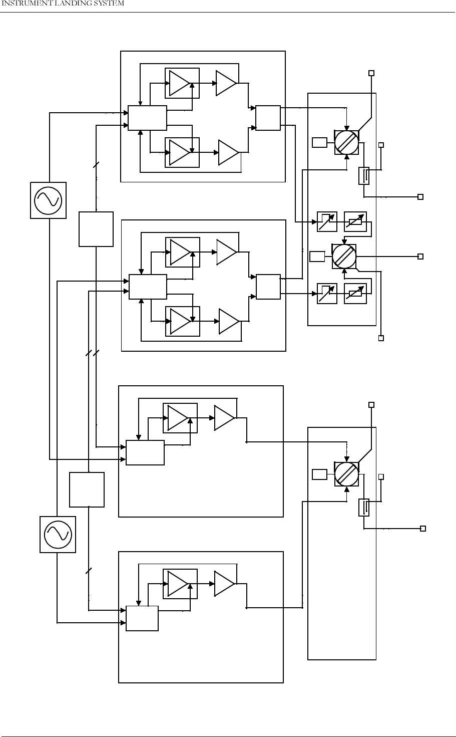
)81&7,21$/'(6&5,37,21
1250$5&
1DYLD$YLDWLRQ$6
7(&+1,&$/+$1'%22.
Figure 8-2 System Block Diagram of a 2-Frequency GP Transmitter
PHASER ATTENUATOR
PHASER ATTENUATOR
COAX
RELAY
COAX
RELAY
CSB
CSB
SBO
SBO
OUTPUT
SBO COURSE
OUTPUT
CSB COURSE
MONITOR
CSB
COUPLER
COAX CONTROL
COAX CONTROL
COAX
RELAY
OUTPUT
CSB CLEARANC
E
MONITOR
CSB
COUPLER
COAX CONTROL
RF OSC.
TX2
RF OSC.
TX1
LF GEN.
TX1
LF GEN.
TX2
CHANGE
OVER COU
CHANGE
OVER CLR
CSB
CSB
POWER AMPLIFIER ASSEMBLY COU-TX2
POWER AMPLIFIER ASSEMBLY COU-TX1
POWER AMPLIFIER ASSEMBLY CLR-TX1
POWER AMPLIFIER ASSEMBLY CLR-TX2
AMPLITUDE FEEDBACK
AM-MOD. HPA
FEEDBACK
CONTROL
AMPLITUDE FEEDBACK
AM-MOD. HPA
FEEDBACK
CONTROL
AMPLITUDE & RF PHASE FEEDBACK
AM-MOD. HPA
HPA
HYBRID
FEEDBACK
CONTROL
AM-MOD.
AMPLITUDE & RF PHASE FEEDBACK
50 ohm
50 ohm
50 ohm
AMPLITUDE & RF PHASE FEEDBACK
AM-MOD. HPA
HPA
HYBRID
FEEDBACK
CONTROL
AM-MOD.
AMPLITUDE & RF PHASE FEEDBACK
HBK 591-1
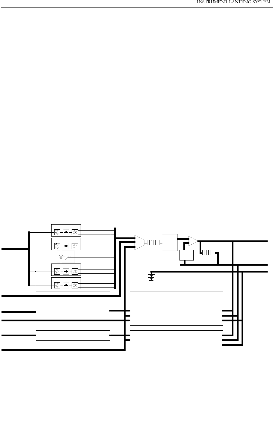
1250$5&7(&+1,&$/+$1'%22.
)81&7,21$/'(6&5,37,21 1DYLD$YLDWLRQ$6
8.3 Monitor
The monitor section’s main task is to generate alarms if the transmitters fail. The alarm signals
are interpreted by the station control section which decides whether to change transmitter or
to shut the ILS signals down. Warning information is treated by the RMS.
The input signals to the monitor are RF signals, CL, DS, NF, CLR(2 freq. only), from the
antenna system. In addition the DC loop detects failures in the antenna and an optional exter-
nal frontend may monitor alarm generating parameters from additional equipment (i.e. a far
field monitor). The outputs are alarm status to the transmitter control section, parameter val-
ues to the RMS and DC loop reference voltages to the antenna system.
The monitor chain consists of the Monitor Frontend module, MF1211A in LLZ and MF1219A in
GP, and the Monitor module MO1212A. This chain is duplicated to increase reliability. In
hot
standby
configurations an additional chain monitors the standby transmitter. See the figure
below.
The
Monitor Frontend
module is mainly an AM receiver which detects the baseband signals
and generates DC voltages proportional to the RF level. In addition a digital pulse train is gen-
erated, to tell the difference in frequency (DF) between the COU and CLR transmitters in
two
frequency
configurations.
The
Monitor
module digitizes the analog signals, filters all data by FFT or mean value calcu-
lations, and passes the parameters to the comparator. The comparator generates alarm sig-
nals if the parameters are outside the programmed limits.
Figure 8-3 Monitor section block diagram.
8.4 Transmitter Control
The transmitter control sections main purpose is to control the transmitters on/off state. This is
done based on alarm inputs from the monitors, inputs from remote control, inputs from local
keyboard (front panel for station control) and inputs from the RMM system.
The station control receives alarm information from the monitors. Based on the alarm status
DS_RF
External Frontend 1
DC loop
FIFO
MUX Digital
Filters
Comp. Alarm bus
RMS bus
DC loop
External Frontend 2
NAV
Mon.1
NAV Mon.2
NAV Mon.St.by
AM receiver
CL_RF
AM receiver
CLR_RF
AM receiver
NF_RF
AM receiver
Mixer
FIFO
Limit
Storage
MONITOR FRONTEND 1 MONITOR 1
MONITOR FRONTEND 2
STANDBY MONITOR FRONTEND
MONITOR 2
STANDBY MONITOR
DS_RF_LEVEL
DS_BASEBAND
CL_RF_LEVEL
CL_BASEBAND
DF
CLR_RF_LEVEL
CLR_BASEBAND
NF_RF_LEVEL
NF_BASEBAND
(SC/TRM)
HBK556-1
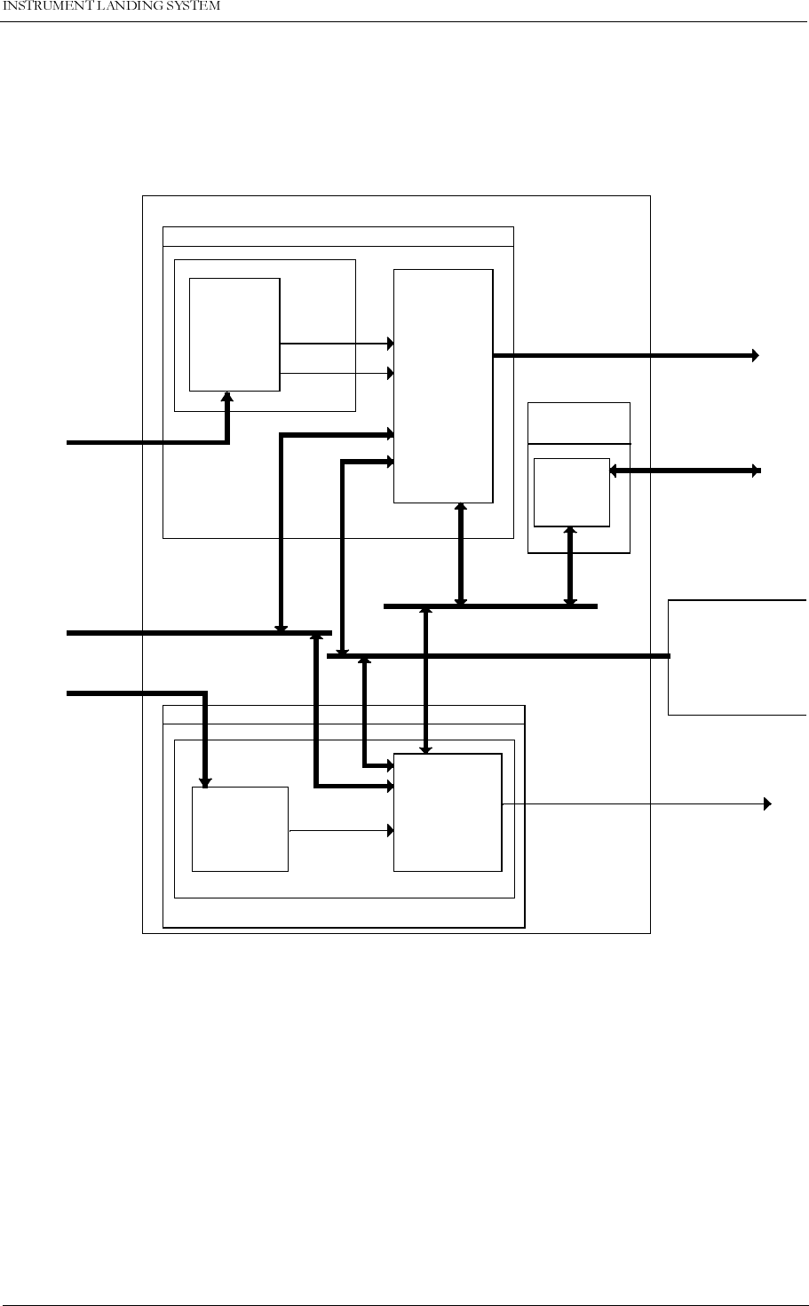
)81&7,21$/'(6&5,37,21
1250$5&
1DYLD$YLDWLRQ$6
7(&+1,&$/+$1'%22.
and the current mode of operation, the station control decides if a changeover/shutdown
should occur. The station control unit also receives user/state inputs from remote control
(example: Interlock) and the RMM system (example: Warning lamp outputs). Configuration
selections on the TC1216A board also affects the operation of the station control.
Figure 8-4 TCA1218A/B Block Diagram
The transmitter control assembly, TCA1218A/B consists of the transmitter control (TC) mod-
ule TC1216A and the local control (LC) front panel LC1217A/B (the B-version is a front panel
designed for hot standby configuration). See Figure 8-4.
The main functions of the TCA1218A/B are performed by the station control (SC) part of the
transmitter control (TC). The SC takes care of the normal operating tasks like turning transmit-
ters on/off bases on various inputs that may affect the transmitter status. The SC also has a
RMS interface enabling the RMM system to read the status of the SC and to illuminate warn-
ing lamps etc.
The terminator (TRM) part of the TC takes over and shuts the ILS down if the SC is not able to
operate as expected. The TRM shut down the power to the transmitters approximately 1 sec-
TX CONTROL
TERMINATOR
SHUTDOWN
UNIT
ALARM
RC bus
REMOTE
CONTROL
INTERFACE
TERMINATOR
STATION CONTROL
CONTROL
AND
UART
ALARM
DETECTION
AND
VOTING
ALARM
STANDBY
ALARM
ALARM
DETECTION
AND
VOTING
Terminator alarm
LOCAL bus
RMS bus
Terminator
alarm bus
TX control bus
RC i/f bus
TC1216A
LC1217A/B
Station control
alarm bus
Local Controls
with/without
hot standby LEDs
Transmitter Control
HBK543-1
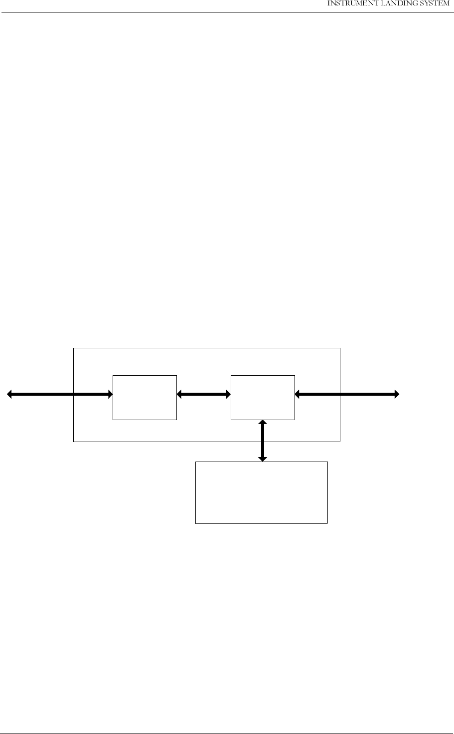
1250$5&7(&+1,&$/+$1'%22.
)81&7,21$/'(6&5,37,21 1DYLD$YLDWLRQ$6
ond after an alarm situation or interlock state has occurred.
The remote control interface process serial data from/to the remote control. This unit also
detects and reports faults in data transmission with remote control. The data from the remote
control are sent to both SC and TRM.
The local control displays the transmitter status of the ILS. It also provides a user interface,
enabling the user to perform basic operations on the ILS.
8.5 Remote control system
The remote control’s main purpose is to provide an interface to the ILS from the control tower,
or technical equipment room at the airport.
The remote control provides the ILS with user inputs and selections. The unit also displays the
status of the ILS using LEDs.
The remote control system consists of an UART/line interface, RC1241A, a front panel,
RF1242A/B (B is a front panel for hot standby configuration) and a slave panel.
The remote control assembly, RCA1240A/B, consists of the remote control (RC) module
RC1241A and the remote control front panel (RF) RF1242A/B (the B-version is a front panel
designed for hot standby configuration). See Figure 8-5.
Figure 8-5 RCA1240A/B Block Diagram
The line interface in RC1241A convert signals between standard serial data format and tele-
phone line signals both ways using a FSK modem (compatible with CCITT V.21).
The UART /control in RC1241A performs serial/parallel conversion. Pushbutton, switch and
operational mode (interlock) status is sent from remote control to ILS. Transmitter status and
other info is received from the ILS.
The front panel RF1242A/B contains the pushbuttons, switches and LEDs for the user.
The slave panel is an optional control panel with a limited set of functions/LEDs, designed for
use in the airport tower.
LINE
INTERFACE
RF1242A/B
Telephone
line CONTROL
AND
UART
Slave bus
Remote Control front panel
with/without hot standby
lamp indications
RC1241A
Slave panel(s)
HBK544-1
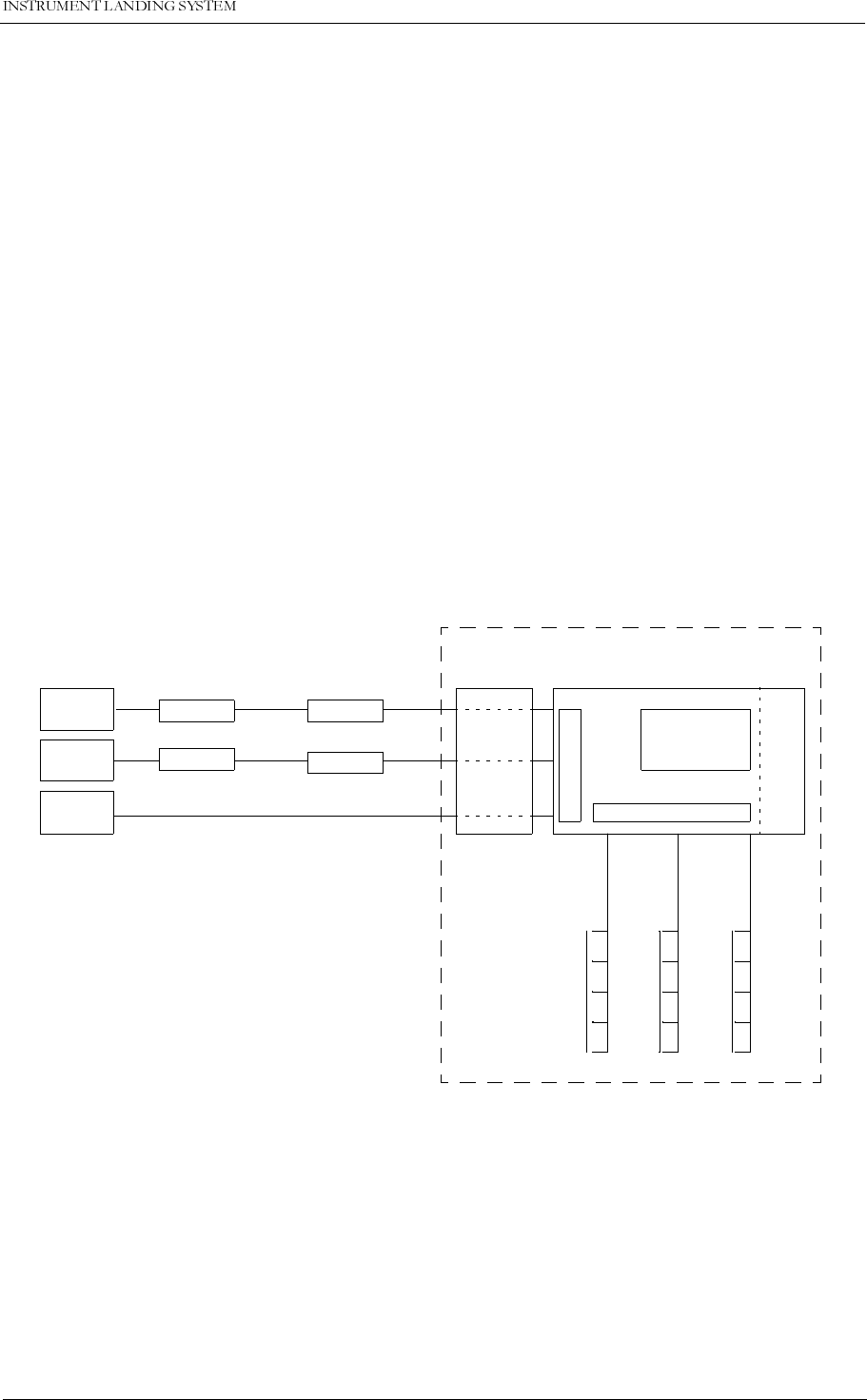
)81&7,21$/'(6&5,37,21
1250$5&
1DYLD$YLDWLRQ$6
7(&+1,&$/+$1'%22.
8.6 Remote Monitoring System (RMS)
8.6.1 General Description
The Remote Monitoring System consists of a CPU-board located inside the main cabinet, with
several means of collecting data from both inside and outside the equipment. The RMS also
constitutes the operator interface, offering up to three RS232 interfaces, and the Local Key-
board/Display. The main tasks are:
• Collection of executive monitor parameters and maintenance parameters
• Generation of system warnings
• Maintaining historical storages of all data.
• ‘Snap-shot’ of all monitor and maintenance data immediately before alarm occurrence.
• Setting of alarm limits and tx parameters.
• Fault isolation.
• Controlling the Local Keyboard/Display.
The RMS SW comprises a resident part located in the ILS. It communicates with the RMM PC
program via dedicated lines or a MODEM. The PC SW is the main operator interface with the
ILS.
Data collection is facilitated in 3 different ways: A parallel high speed data bus offering both
read and write operations, a IIC-standard serial bus, and a set of 24 different ADC channels.
Figure 8-6 The RMM configuration.
8.6.2 PC and Modem
The main operator interface is locally or remotely connected personal computers, running
dedicated SW and communicating with the main cabinet resident SW via a dedicated proto-
col. The system facilitates three channels for PC connections, two of which can be used for
remote PC via modems and leased-line or dial-up telephone lines. All three PC’s can be
logged on simultaneously, but only one of them can have write access at a given point in time.
RMA 1215ARemote
PC 2
Remote
PC 1
Local
PC
RS232
RS232
RS232 RS232
RS232
RS232
Dial-up
or
leased-line
IIC
serial bus
Analog
channels
RMS
data bus
CI 1210A
Local
Remote 1
Remote 2
Serial Interface
Interface Circuitry
LCD / Keyboard
CPU
MAIN CABINET
MODEM
MODEM
MODEM
MODEM
Digital
and
Analog
Inputs
Analog
Inputs
Monitor
Data
and
System
Settings
HBK569-1

1250$5&7(&+1,&$/+$1'%22.
)81&7,21$/'(6&5,37,21 1DYLD$YLDWLRQ$6
8.6.3 RMS Databus
The main operation of the RMS parallel data bus is continuously to collect data from the Mon-
itor MO 1212A. Additional functions are setting of monitor alarm limits and delays on the MO
1212A, setting of TX-parameters on LF-generator LF1223A, and reading of system status
from the TX Control Assembly TCA 1218A/B. Writing of warning status to the TCA 1218A/B is
also done via the RMS databus.
Figure 8-7 The RMS databus.
8.6.4 Maintenance Data Collection
In order to facilitate fault isolation and presentation, several analog and digital measuring
points are distributed throughout the system. These point are primarily accessed via the IIC
serial bus. In addition, 24 ADC-channels are read directly into the RMA 1215A board.
The IIC serial bus collects digital status information from MF1219A, MO1212A, LF1223A,
OS1221B and the CI 1210A connection interface card. 6 of these are user configurable
inputs/outputs. In addition, analog measurements are obtained from the GP - Power Assem-
blies GPA1231A and GPA1232A.
The ADC-channels are mainly used to measure power amplifier current consumptions, as well
as system voltages. These measurements are obtained from the Power Supply boards
PS1227A. In addition system current consumption, as well as several user configurable
inputs, are measured on the CI1210A board.
RMA 1215A
MO 1212A
MON1
MO 1212A
MON2
LF 1223A
TX1
LF1223A
TX2 TCA 1218A/B
RMS Databus
MO 1212A
STB MON
HBK568-1

)81&7,21$/'(6&5,37,21
1250$5&
1DYLD$YLDWLRQ$6
7(&+1,&$/+$1'%22.
Figure 8-8 The IIC serial bus and ADC channels.
8.7 Power Supply
The ILS main cabinet is supplied from one or two 27V power supplies with a backup battery.
The 27V is regulated down to ±15V, 8.5V and 5V. The transmitter power amplifiers are fed
directly from the 27V supply, while the rest of the system uses the regulated voltages.
Current measurements are done on the power supply, the battery and each power amplifier.
Each regulated voltage is measured in the Power Supply PS1227A. The results are presented
to the user through the RMS system.
When the ILS signals are shut down, the power supply to the power amplifiers are actually
turned off by relays. This is controlled by the
terminator alarm
signal from the station control
section.
The backup battery is protected against deep discharge with a protection circuit. This circuit
disconnects the battery when the voltage drops below 22V.
A battery warning is given through the RMS system when the primary power supply (supplies)
fails.
RMA 1215A
MF 1219A
MON1 MF 1219A
MON2 MO 1212A
MON1 MO 1212A
MON2 PS 1227A #1 PS 1227A #2
LF 1223A
TX1 LF 1223A
TX1 GPA 1231A
TX1 COU GPA 1232A
TX1 CLR GPA 1231A
TX2 COU GPA 1232A
TX2 CLR
CI 1210A
IIC serial
bus
ADC
channels
MF 1219A
STB MON MO 1212A
STB MON
OS 1221B
TX1 OS 1221B
TX2
HBK571-1
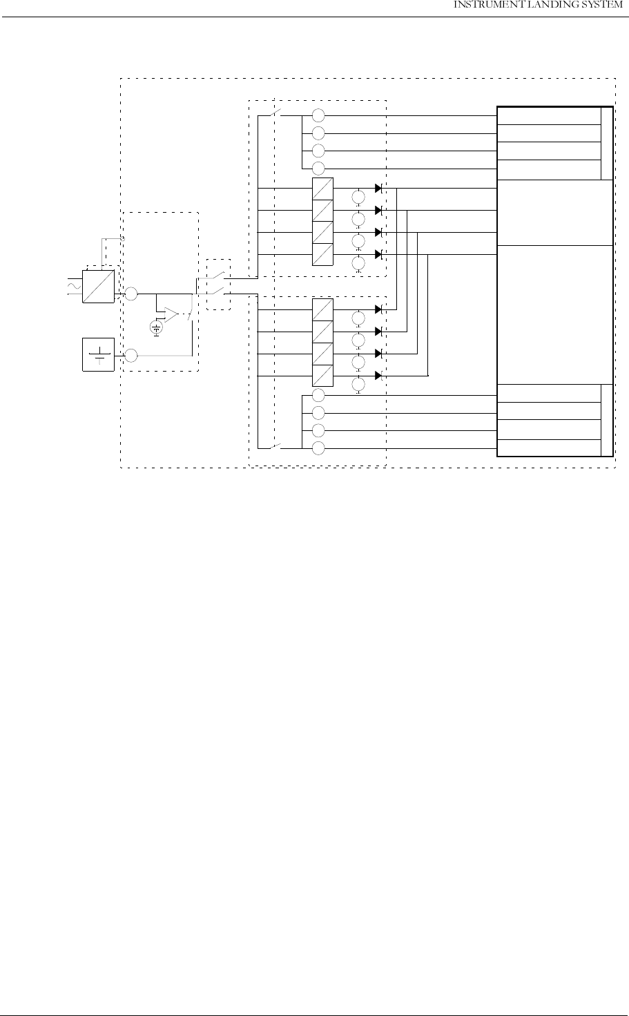
1250$5&7(&+1,&$/+$1'%22.
)81&7,21$/'(6&5,37,21 1DYLD$YLDWLRQ$6
.
Figure 8-9 Power supply functional diagram.
A
A
AC
DC
DC
DC
DC
DC
DC
DC
DC
DC
Terminator
Alarm
DC
DC
DC
DC
DC
DC
DC
DC
MODULE CONNECTIONS
TX1 TX2
PA123xA CL 90Hz
PA123xA CL 150Hz
PA123xA CLR 90Hz
PA123xA CLR 150Hz
PA123xA CL 90Hz
PA123xA CL 150Hz
PA123xA CLR 90Hz
PA123xA CLR 150Hz
MF121xA
MO1212A
RMA1215A
LF1223A
OS1221x
CI1210A
AC1226A
TCA1218A
Main
Cabinet
Switch
CI1210A
PS1227A-1
PS1227A-2
V
V
V
V
V
V
V
V
+
--
A
A
A
A
A
A
A
A
Battery Warning
V27_CL1501
V27_CL901
V27_CLR901
V27_CLR1501
V15P
V15N
VDD
V8P5P
V27_CL1502
V27_CL902
V27_CLR902
V27_CLR1502
MF121xA
OS1221A
xPA123xA
MAIN CABINET
HBK584-2

'(7$,/(''(6&5,37,21
1250$5&
7(&+1,&$/+$1'%22.
1DYLD$YLDWLRQ$6
9 Detailed description
This chapter gives a detailed description of the assemblies and modules in the NM7033.
Notations in the block diagrams:
~ - Active low signal.
[7:0] - Signal bus numbering system. Here, an
eight bits bus, numbered from seven
down to zero.
9.1 Main Cabinet
The following paragraphs describe the electronics modules located in the main cabinet.
9.1.1 MF1219A Glidepath Monitor Frontend
General Description:
The MF1219A module demodulates the ILS RF signals from the antenna system, and passes
baseband and RF level signals, and a digital pulstrain representing the difference in frequency
(DF) between the CL and CLR signals, to the monitor MO1212A (chapter 9.1.2). The CLR
channel and DF circuit are used in two frequency systems only.
Block Diagram:
See Figure 9-1.
Block Description:
The MF1219A module has four identical channels:
• DS - Displacement Sensitivety
• NF - Near Field
• CL - Course Line
• CLR - CLeaRence
In addition a mixer circuit extracts the difference frequency between CL RF and CLR RF, and
a maintainance monitor reports low level RF amplitude and modulation depth to the RMS.
CL_FILT
consists of a step attenuator and a bandpass filter covering the bandwith 328-336 MHz. The
step attenuator can be set in the range 0 to 34 dB by setting jumper plugs enabling one or
more of three attenuators each providing 6dB, 12dB and 16 dB attenuation.
CL_RFAMP
splits the band limited RF signal to the baseband chain and the RF level chain. The baseband
amplifier stage comprises automatic gain control (AGC) through a pin diode attenuator.
CL_LEV
detects a DC voltage proportional to the RF input level, through a detector diode and a low
pass filter.
CL_BASEB
detects the baseband signals and generates the control voltage to the AGC stage of the
CL_RFAMP. When no RF signal is present, the AGC voltage is clamped to a preset level.

1250$5&7(&+1,&$/+$1'%22.
'(7$,/(''(6&5,37,21 1DYLD$YLDWLRQ$6
CL_LPFI
are active lowpass filters that attenuates frequencies above the ILS baseband.
DF_MIXER
mixes the CL and CLR RF signals and extracts the difference frequency. The output signal is
a TTL level pulse train.
MAINTMON
monitors the RF levels and the modulation depths, and reports to the RMS if the levels exceed
the preset limits.
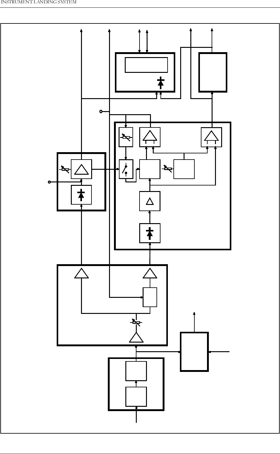
'(7$,/(''(6&5,37,21
1250$5&
7(&+1,&$/+$1'%22.
1DYLD$YLDWLRQ$6
.
Figure 9-1 MF1219A Block diagram (CL channel shown)
CL_BASEB
CURRENT-
CONTROLLED
ATTENUATOR
CL_RFAMP
RF LEVEL
VERNIER
STEP
ATTENUATOR
BANDPASS
FILTER
CL_FILT
LOWPASS FILTER
BASEBAND
RF INPUT
CL_LPFI
DF_MIXER
ACTIVE MIXER
From CLR channel
DF
LOWPASS
FILTER
PRESET
AGC LEVEL
RF LEVEL
DC OUT
CL_LEV
RF LEVEL
AGC
MUX
Part of MAINTMON
CL_IDENT
IIC_SDA
IIC_SCL
VOLTAGE
REFERENCE
COMPARATOR
AGC_VOLT
TP 1...4
TPxx23
AGC_TIME
HBK554-2

1250$5&7(&+1,&$/+$1'%22.
'(7$,/(''(6&5,37,21 1DYLD$YLDWLRQ$6
9.1.2 MO1212A Monitor
General Description:
The MO1212A module digital converts and processes NAV parameters, compares them with
programmable limits and reports alarm situations to the Station Control on TCA1218A (chap-
ter 9.1.3) and the RMS.
Block Diagram:
See Figure 9-2.
Block Description:
LF_FRONT:
The analog signals from MF1219A Monitor Frontend are multiplexed and digitized, and the
difference frequency (DF) pulse train is counted as a 12 bits value. These digital values are
multiplexed into the FIFO along with the DC loop (DL_Detect[3:0]), External (Ext_Val[11:0])
and test channels. The FIFO is seven words deep, and the sampling frequency is 640 Hz/
channel. Much of the functionality of LF-Front is handled by a FPGA NMP101A which is
described in chapter 9.1.2.1.
DSP_FILTER
performs all filtering in the Monitor. Data is read from the LF_FRONTEND FIFO, AC data are
FFT analyzed and for the DC data mean values are calculated. The calculated parameters
are written to the COMPARATOR. DSP_FILTER consists of a TMS320C31 DSP, a memory
block and a reset/watchdog circuit.
COMPARATOR
compares the parameters received from DSP_FILTER with the programmed upper and lower
alarm limits. Alarm data are passed on to the Station Control and Terminator (on TCA1218A,
chapter 9.1.3) on a dedicated bus. The COMPARATOR generates both instantanous and
delayed alarms. The delayed signal is sent only if the alarm is still present after the pro-
grammed delay period. All parameters, alarm and warning data are passed on to the RMS via
an output FIFO (warning information is treated by the RMS). The alarm and warning limits and
delays are stored in the local EEPROM. Much of the functionallity of COMPARATOR is han-
dled by two FPGAs NMP102A and NMP103A described in chapter 9.1.2.2.
9.1.2.1 NMP101A Monitor Digital Frontend
General description:
NMP101A is a FPGA in the LF-FRONT block. It serves as an interface between the (digi-
tized) inputs from the monitor frontend MF1219A and the DSP_FILTER block. NMP101A is
based on the Actel ACT1020 FPGA. For electrical specifications see the ACT1020 datasheet.
Block diagram:
See Figure 9-2.
Block description:
REF COUNTER
divides the system clock (4.9152 MHz) for use in channel addressing. It also generates the
read/convert puls to the external ADC.

'(7$,/(''(6&5,37,21
1250$5&
7(&+1,&$/+$1'%22.
1DYLD$YLDWLRQ$6
DIFF FREQ COUNTER
counts the pulse train that represents the frequency difference between the CL and CLR sig-
nals. It generates a 12 bits value which multiplied by 20 gives the true frequency difference.
MUX
selects between DF, one of sixteen channels from the ADC or one of the eight external chan-
nels in a roundabout manner to the FIFO.
FIFO
is a 7x17 bits first in first out queue with interface to the TMS320C31 DSP in the DSP_FILTER
block. The five most significant bits are channel address and the 12 least significant bits are
data. FIFO reports error to the COMPARATOR and data available (DAV) status to the DSP.
9.1.2.2 NMP102A / NMP103A Comparator
General description:
NMP102A and NMP103A are two FPGA’s providing most of the functionallity of the COM-
PARATOR block.
Block diagram:
See Figure 9-2.
Block description:
The block diagram shows both the NMP102A and NMP103A as a whole and blocks drawn
twice are found with the same functionallity on both FPGA’s.
INPUT LATCH:
stores the parameter number and value coming from DSP_FILTER.
SEQUENCE CONTROLLER:
Controls the entire operation of reading alarm limits from the EEPROM, runs parity checks on
the alarm limit values, compares the parameter value from DSP_FILTER with upper and lower
alarm limits, reads and parity checks the alarm delay values and delays any alarms corre-
spondingly.
COMP:
Compares the parameter value from DSP_FILTER with the alarm limits from EEPROM and
generates a raw alarm.
DELAY:
Delays the raw alarms corresponding to the delay values in the EEPROM.
FIFO CONTROL:
Writes data into the FIFO when the comparator cycle is finished.
EEPROM INTERF.:
Controls the interface towards the EEPROM. EEPROM write is only allowed if RMS_LEVEL1
is a logic '0' (RMS access level3).
RMS INTERF:

1250$5&7(&+1,&$/+$1'%22.
'(7$,/(''(6&5,37,21 1DYLD$YLDWLRQ$6
Is the interface to the RMS. It controls interrupt when data is ready in the FIFO and generates
addresses for EEPROM programming and status and control signals.
PARITY CHECK:
Checks incoming data from the EEPROM. One bit error is corrected, and only a parity warning
is passed to the RMS. If two bits are erroneous, all output alarms are set, and a parity error is
passed to the RMS.
EEPROM:
The EEPROM is used to store the alarm limits. Warning limits used by the RMS are also
stored here.
FIFO:
The FIFO is used to streamline the data transfer to the RMS. One full set of 32 parameters is
written to the FIFO before the interrupt is activated.
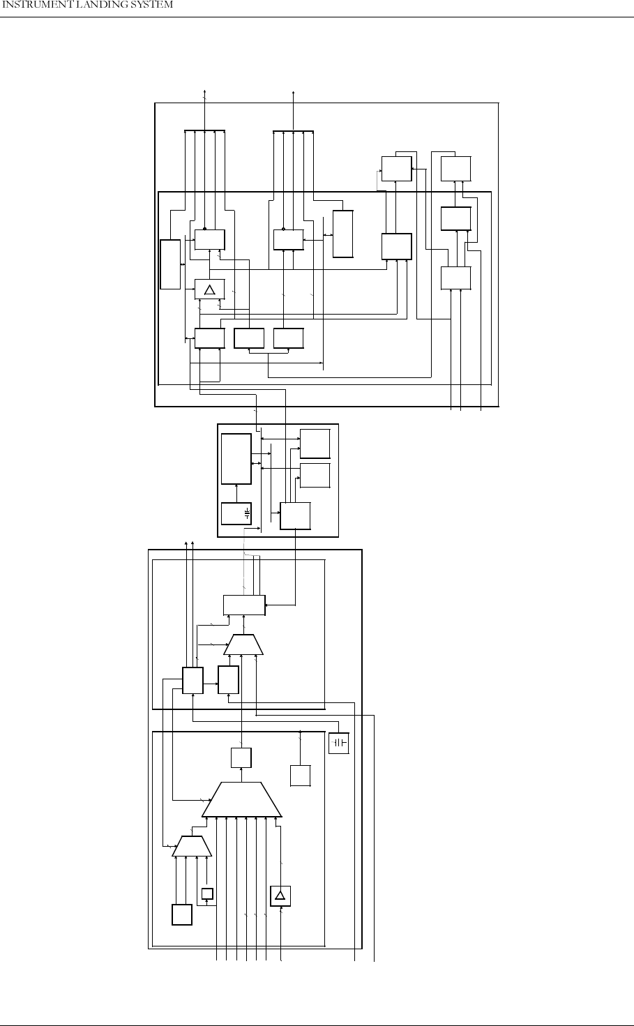
'(7$,/(''(6&5,37,21
1250$5&
7(&+1,&$/+$1'%22.
1DYLD$YLDWLRQ$6
Figure 9-2 MO1212A Blockdiagramm
LF_FRONT
ANAFRONT
CL_RFLEVEL
CL-BASEBAND
CL_IDENT
DS_*
NF_*
CLR_*
DL_DETECT_*
2
2
3
4
TEST_RF_ERROR
TEST_RF_OK
LPF CL_BB_DGR
2
2
4
TST_CH[1:0]
MUX
ANA_CH[3:0]
AD
12
ADO[11:0]
DF
NMP101
REF
COUNTER
DIFF
FREQ
COUNTER
MUX FIFO
CLK
17
5
55
12
12
EXT_VAL[11:0]
LF_DREAD
FULL
DO[16:0]
DAV
EXT_CH[2:0]
EXT_ENA
4
RESET
AND
CHECK
CIRCUIT
DIGITAL SIGNAL
PROCESSOR
ADDRESS
DECODER
BOOT
EPROM EXTERNAL
RAM
DSP_FILTER
SEQUENCE
CONTROLLER
INPUT
LATCH
COMP
DELAY
PARITY
CHECK
PARITY
CHECK DELAY
FIFO
CONTROL FIFO
WR
RD
RMS
INTERF. EEPROM
INTERF. EEPROM
MONITOR
TER ALARM
BUS
NMP 102/103A
MS_ALARM_RDY
MS_ALARM_RAW
MS_AL
MS_AL_N
MS_AL_ID[4:0]
MT_AL_RDY
MT_AL_N
MT_AL
MT_AL_ID[4:0]
MT_AL_RDY
IOD[7:0]
IOS[6:0]
RMS_LEVEL1
PAR_WR
DSP_DATA[11:0]
DSP_DATA[16:12]
12
4 4
5
5
4
COMPARATOR
FROM
MF1211A
4
MUX
17
RMS BUS
FROM
TCA1218A
MONITOR
SC ALARM
BUS
9TO
TCA1218A
TO
TCA1218A
4.9152 MHz
VOLT.
REF.
VOLT.
REF.
DL_REF*
HBK555-2
SEQUENCE
CONTROLLER

1250$5&7(&+1,&$/+$1'%22.
'(7$,/(''(6&5,37,21 1DYLD$YLDWLRQ$6
9.1.3 TCA1218A Transmitter Control Assembly
General Description:
The TCA1218A transmitter control assembly consists of the transmitter control TC1216A and
Local Control (front panel) LC1217A.
Block Diagram:
See figure Figure 9-3 and Figure 9-4. All blocks except Local Control are located on
TC1216A.
Description of selected signals:
MON1 SC ALARM BUS :
Station control alarm bus from monitor MO1212A no.1. Consists of M1S_AL_ID[4:0],
~M1S_AL_RDY, M1S_AL, ~M1S_AL_N and M1S_AL_RAW.
MON2 SC ALARM BUS :
Station control alarm bus from monitor MO1212A no.2. Consists of M2S_AL_ID[4:0],
~M2S_AL_RDY, M2S_AL, ~M2S_AL_N and M2S_AL_RAW.
STB MON ALARM BUS :
Station control alarm bus from standby monitor MO1212A. Consists of ~MSTBS_AL_RDY
and MSTBS_AL. Only used for hot standby configurations.
RMS BUS :
Interface to the RMS. Consists of IOD[7:0], IOCS, IOS[2:0].
MON1 TRM ALARM BUS :
Terminator alarm bus from monitor MO1212A no.1. Consists of M1T_AL_ID[4:0],
~M1T_AL_RDY, M1T_AL, ~M1T_AL_N and M1T_AL_RAW.
MON2 TRM ALARM BUS :
Terminator alarm bus from monitor 2. Consists of M2T_AL_ID[4:0], ~M2T_AL_RDY, M2T_AL,
~M2T_AL_N and M2T_AL_RAW.
RC_BUS :
Interface to the line interface circuits for the remote control interface on CI1210A (ch 9.1.11).
Consists of SDIN, SDOUT, ~CD.
Block Description:
STATION CONTROL
interpret the alarm bus from the monitors MO1212A and generates alarm (and standby alarm
for hot standby configurations). These signals together with inputs from local controls (on
LC1217A), remote controls (via CI1210A), RMS inputs and configuration setup (in EEPROM
and jumper settings) determine the state/state change for the NM70xx transmitter state. Sta-
tus information are generated and sent to local control panel (LC1217A) and remote control
panel (via CI1210A). The RMS can poll the state of the station control at any time. State
changes generates an interrupt signal to the RMS. STATION CONTROL can shut off the
transmitters GPA1231/1232A by turning off the RF-oscillators OS1221B.

'(7$,/(''(6&5,37,21
1250$5&
7(&+1,&$/+$1'%22.
1DYLD$YLDWLRQ$6
Most of the functionality of STATION CONTROL is handled by three FPGAs NMP104A,
NMP105A and NMP106A described in chapters 9.1.3.1 - 9.1.3.3.
TERMINATOR
interpret the alarm bus from the monitors MO1212A and generates alarm. This signal together
with local controls (on LC1217A, remote controls (via CI1210A), RMS inputs and configuration
setup (in EEPROM and jumper settings) determine the state of the terminator alarm
(TRM_AL) output. TERMINATOR has an extra 1s delay, so that the STATION CONTROL has
time to fulfill transmitter state changes before the terminator shuts the NM70xx down. Termi-
nator alarm shuts the NM70xx down by disconnecting the power supply from the output stage
of the transmitters GPA1231/1232A.
Most of the functionality of TERMINATOR is handled by FPGA NMP107A described in chap-
ter 9.1.3.4.
REMOTE CONTROL IF:
This unit converts signals from the station control and terminator to serial messages (1 mes-
sage is 2 bytes long). This is done continuously (approximately 10 messages/s). The serial
input from the remote control is converted to parallell format. Messages from the remote con-
trol are accepted only if two equal messages are received in sequence. If no valid message is
received within 2s, the remote control interface assert a failure signal to inform the station con-
trol and terminator that the link to the remote control is broken. Depending on the configura-
tion setup, this will turn the NM70xx off.
CONFIG
Jumper plugs for configuration of the NM70xx.
DEBOUNCE
consists of debouncing circuitry for signals from switches on LC1217A and jumper plugs for
setting access levels for remote control.
LOCAL CONTROL
consist of keys, switches, switchlocks lamps and indicators located on LC1217A used to con-
trol and indicate operational status of the NM70xx.
9.1.3.1 NMP104A Station Control Monitor Data Detector
General Description:
NMP104A is a FPGA within the STATION CONTROL block. It serves as a monitor alarm/error
detection and monitor alarm voting unit. NMP104A is based on the Actel ACT1020 FPGA. For
electrical specifications see the ACT1020 datasheet.
Block Diagram:
See Figure 9-3 and Figure 9-4.
Block Description:
MON.1 ALARM & ERROR DETECTION
This block decodes the MON1 SC Alarm bus and generates alarm if the monitor MO1212A no
1 has set the alarm flag for any of the 32 parameters received in a set. Error checks includes
parameter identity sequence check, AL_N negated of AL, test channel alarm toggling and tim-
eout for RDY-signal. Any alarm/error will set the monitor alarm output (M1_ALARM) for the

1250$5&7(&+1,&$/+$1'%22.
'(7$,/(''(6&5,37,21 1DYLD$YLDWLRQ$6
duration of next 32 parameters, meaning that 32 parameter without alarm/error must be
received in sequence before the alarm output is reset.
MON.2 ALARM & ERROR DETECTION
Same as for MON.1 ALARM & ERROR DETECTION, but for MON2 SC alarm bus.
VOTING
This block provides monitor alarm (VALARM) to the NMP105A depending on jumper configu-
ration (1 of 2 or 2 of 2 voting) in the CONFIG block and inputs from the two MO 1212A moni-
tors (not including standby monitor). When configured for 2 of 2 voting, both MO 1212A
monitors must give alarm to set the VALARM output. When configured for 1of 2 voting, alarm
from one of the two MO 1212A monitors is sufficient to set VALARM.
STB ALARM DETECTION
Alarm flag for any parameter sets the alarm immediately. The alarm will be reset when 32
parameters are received in sequence with no alarm flag set.
PUSHBUTTON ONESHOTS
To prevent locking up of push button keyboard signals, this block translates the input signals
from the switches on LC1217A from levels (high or low) to pulse stream.
9.1.3.2 NMP105A Station Control Event Detection
General Description:
NMP105A is a FPGA within the STATION CONTROL BLOCK. It serves as an event detection
and control unit. The NMP105A also includes the station control RMS-interface. The event
information is output to the station control state machine controller NMP106A. NMP105A is
based on the Actel ACT1020 FPGA. For electrical specifications see the ACT1020 datasheet.
Block Diagram:
See figure Figure 9-3
Block Description:
RMS INTERFACE
The RMS interface provides interface to the RMS BUS
LAMP STATUS GENERATION
This block generates lamp status information for the LOCAL CONTROL and REMOTE CON-
TROL IF blocs.
RMS LEVEL DETECT
This block decodes RMS access levels 2 and 3 using access configuration in CONFIG block,
write disable switchlock information from LOCAL CONTROL, access grant from Remote Con-
trol IF and access requests from the RMS.
EVENT DETECT
The event detect unit checks for valid events (for example key press, alarm interlock etc.), and
sends valid event number to the station control state machine controller NMP106A. Events
not valid for the current mode of operation are ignored. Events are given priorities with inter-
lock as the highest priority. The alarm event has the next priority, while the other events are

'(7$,/(''(6&5,37,21
1250$5&
7(&+1,&$/+$1'%22.
1DYLD$YLDWLRQ$6
polled one by one. The event detect unit also has a built in integrity check. This function
works when the ILS is in normal operational mode (automatic mode with transmitters on and
no alarm). When the ON/OFF is pressed, a FORCE_AL signal is output. This signal turns off
all transmitters (PA 1234A) without notifying the rest of the system. The loss of transmitted
signal will be detected by the monitors (MO 1212) and cause monitor alarms to the STATION
CONTROL.This alarm will result in a TX changeover initiated by STATION CONTROL, but
since STBY TX is also turned off, monitor alarm will remain and cause TX shutdown after
alarm delay. This sequence ensures that the monitoring circuits and shutdown mechanisms
operates as intended. If the integrity check function should fail, a timeout function shuts the
ILS down.
INTERRUPT DETECT
This block detects transmitter state changes and stores the event causing the change. Trans-
mitter feedback and coax relay position is also stored. An interrupt is generated to inform the
RMS that a transmitter state change has occurred.
TX 20 SEC DELAY
This function ensures that no transmitters are allowed to transmit for 20 seconds after an
alarm shutdownhas occured.
MAIN SELECT STORE
This block stores the information regarding which transmitter that is selected as main transmit-
ter.
INTERLOCK DELAY
This block turns on the transmitters 20 seconds after the interlock signal from the REMOTE
CONTROL IF block has been deactivated.
9.1.3.3 NMP106A Station Control State Machine Control
General Description:
NMP106A is a FPGA within the STATION CONTROL block. It serves mainly as a state
machine controller (states are stored in an EPROM) for transmitter on/off control. NMP106A is
based on the Actel ACT1020 FPGA. For electrical specifications see the ACT1020 datasheet.
Block Diagram:
See Figure. 9-3
Block Description:
SEQUENCER
This block generates strobes and control signals for running the state machine. New states
are triggered based on received new data from NMP105A (on the STO_BUS). This block also
generates reset to the hardware watchdog safeguarding and controlling the station control
reset.
EVENT CHECK
This block checks event and main select signal received from NMP105A. Two identical event/
main select signals must be received in sequence before the event/main select is acted upon.
TIMER

1250$5&7(&+1,&$/+$1'%22.
'(7$,/(''(6&5,37,21 1DYLD$YLDWLRQ$6
Used by the state machine for delays/timeouts for state changes.
DELAY
Delays the coax relay position feedback in state change sequences. Ensures that the coax
relay on COA1207A (Ch.9.1.6) will not change position while the transmitters are transmitting.
PARITY CHECK
This block check the parity of each byte read from the state machine content EPROM. Parity
failure results in transmitter shutdown.
LOCKUP DETECT
This block detects failures in the state machine sequence. It will trigger if the state machine
don’t become idle within a specified time. Failures results in transmitter shutdown.
EPROM READ DATA ADDRESS
This block is an address counter setting the address for the state machine EPROM during
reading through the RMS. The RMS can either reset or increment the adress counter. The
feedback from these control strobes, address bit 0 and EPROM data byte are transferred to
the NMP105A for reading by the RMS.
TX ON/OFF CONTROL
This block controls the on/off state of the transmitters. Default is leaving the transmitters in the
state reported by their feedback signals, thereby providing no change in transmitter state.
However, if PARITY CHECK failure or event LOCKUPDETECT failure is detected, the trans-
mitters are turned off.
LOCAL LAMP STATUS
Local panel lamp outputs to the LOCAL CONTROL BLOCK are provided based on coax relay
position, TX main select, transmitter status and station status received from NMP105A.
EPROM ADDR MUX
This block selects EPROM addressing either for STATE MACHINE or RMS read control.
9.1.3.4 NMP107A Terminator
General Description:
NMP107A is a FPGA providing most of the TERMINATOR function. The terminator function is
to provide a transmitter shutoff function if the STATION CONTROL should fail to do so.
NMP107A is based on the Actel ACT1020 FPGA. For electrical specifications see the
ACT1020 datasheet.
Block Diagram:
See Figure 9-3 and Figure 9-4.
Block Description:
RMS INTERFACE
The RMS interface provides the interface to the RMS BUS.
RMS LEVEL DETECT
This block decodes RMS access levels 2 and 3 using access configuration in CONFIG block,

'(7$,/(''(6&5,37,21
1250$5&
7(&+1,&$/+$1'%22.
1DYLD$YLDWLRQ$6
write disable switchlock information from LOCAL CONTROL, access grant from REMOTE
CONTROL IF and access requests from the RMS.
EVENT DETECT
The event detect unit checks for valid events (for example on/off-key, alarm, interlock etc.),
and sends valid events to the terminator state check. Events not valid for the current mode of
operation are ignored.
TERMINATOR STATE CHECK
This block acts upon events/states received from the EVENT DETECT block. Alarm/interlock
states are allowed to be active for 1 second before terminator alarm is activated. The termina-
tor alarm is then reset if an on/off-event is detected, thereby starting a new 1 second timeout.
The STATION CONTROL must now stabilise the ILS with no alarm within this 1-second period
of time if a TERMINATINATOR shutdown should be avoided. If terminator is triggered by
alarm or interlock while transmitters are transmitting, an interrupt is generated. The RMS can
then read the cause of the interrupt through the RMS BUS.
INTERLOCK FILTER
This block overrides the interlock signal in interlock override mode of operation. To enable
interlock override mode of operation the interlock override switchlock must be activated, the
local/remote switch must be in local position and the auto/manual switch must be in manual
position.
MON.1 ALARM & ERROR DETECTION
This unit decodes the MON1 TRM ALARM BUS and generates alarm if the monitor MO
1212A no. 1 has set the alarm flag for any of the 32 parameters received in a set. Error checks
includes parameter identity sequence check, AL_N negated of AL, test channel alarm toggling
and timeout for RDY-signal. Any alarm/error will set the monitor alarm output (M1ALARM) for
the duration of the next 32 parameters, meaning that 32 parameters without alarm/error must
be received before the alarm output is reset.
MON.2 ALARM & ERROR DETECTION
Same as for MON.1 ALARM & ERROR DETECTION but for MON2 TRM ALARM BUS.
VOTING
This block provides a monitor alarm (~VALARM) depending on jumper configuration (1 of 2 or
2 of 2 voting) in the CONFIG block and inputs from the two MO1212A monitors (not including
STBY monitor). When configured for 2 of 2 voting both MO 1212A monitors must give alarm to
set the ~VALARM output. When configured for 1 of 2 voting alarm from one of the two MO
1212A monitors is suffisient to set the ~VALARM.
9.1.3.5 NMP109A Remote Control Interface
General Description:
NMP109A is a FPGA providing most of REMOTE CONTROL IF function. The NMP109A
transfers data between STATION CONTROL and TERMINATOR and the remote control (via
CI 1210A). NMP109A is based on the Actel ACT1020 FPGA. For electrical specifications see
the ACT1020 datasheet.
Block Diagram:
See Figure 9-3 and Figure 9-4.

1250$5&7(&+1,&$/+$1'%22.
'(7$,/(''(6&5,37,21 1DYLD$YLDWLRQ$6
Block Description:
STB LAMP FILTER
This block provides the standby lamp information to be sent to remote control by the TX
UART.
TX UART
Converts parallel data to 2-bytes serial messages. Protocol for the serial data SDOUT (sent I
1210A) is startbit, 8 databits, 1 stopbit, odd parity.
RX UART
Converts serial data SDIN received from remote control (via CI 1210A) to parallel data (2
bytes).
MESSAGE DETECTOR
Messages from RX UART are accepted only if two idnetical messages are received in
sequence. If so, the data output latch is updated and a new-message pulse is generated.
NEW MESSAGE TIMER
Checks whether an OK message from MESSAGE DETECTOR and carrier detect signal from
CI 1210A is present. Missing message or no carrier detect for 2 seconds or more gives time-
out signal to DATA FILTER.
DATA FILTER
In case the NEW MESSAGE TIMER has signalled a timeout (indicating missing messages)
this block will modify the data received from the MESSAGE DETECTOR by forcing the
TX_OFF signal to on (configurable). If configuration enables interlock, the interlock signal is
also forced active.
'(7$,/(''(6&5,37,21
1250$5&
7(&+1,&$/+$1'%22.
1DYLD$YLDWLRQ$6
Figure 9-3 TCA1218A Block diagram part 1
VOTING_CONFIG
M1S_AL_ID
M1_AL
M1S_AL_N
M1S_AL_RAW
M1S_AL_RDY
MSTBS_AL_RDY
MSTBS_AL
MON1
ALARM
& ERROR
DETECTION VOTING
STB ALARM
DETECTION
PUSH-
BUTTON
ONESHOTS
LCIN[14:0]
MON1 SC ALARM BUS
MON2 SC ALARM BUS
STBMON SC ALARM BUS
M1_ALARM
M1_ERROR
VALARM
M2_ALARM
M2_ERROR
STB_ALARM
LC_INB[14:0]
SC MON DATA DETECTOR
NMP104A
From MO1212
From MO1212
From MO1212
SW1THCES/
PUSHBUTTONS
LEDS
WARN
+
STB LEDS
LC_IN[10:0]
LC1217A
DEBOUNCE
LC_IN[14:11]
CONFIG
TRM CLOCK
SEQUENCER
EVENT
CHECK
TIMER
DELAY
EPROM READ
DATA
ADDRESS
PARITY
CHECK
LOCKUP
DETECT
TX ON/OFF
CONTROL
LOCAL
LAMP
STATUS
SEQUENCE
CONTROL
EVENT NO USED
MAIN SELECT USED
EPROM READ DATA
TIMEOUT
VALUE
TIMER
TRIG
TIMEOUT GONE
EPROM READ DATA
STATE
MACHINE
ADDRESS
COAX POS
EPROM ADDR
PARITY ERROR
DATA BYTES
PENDING
EVENT NO
LOCK
TIMEOUT
TXFB
TXFB
COAXPOS
STATUS LAMPS
MAIN SELECT
SC STATE MACHINE CONTROL
CONFIGURATION
STO_BUS
EPROM DATA
TXON
LC_OUT
COAXPOS
PENDING
ST_BUS
NMP106A
RMS
INTERFACE
RMS
LEVEL DETECT
EVENT
DETECT
INTERLOCK
FILTER
ALARM
AUTO
-ONOFF
-TXONOFF
TERMI-
NATOR
STATE
CHECK
ILOCK_INT
ALARM_INT
MON1
ALARM
& ERROR
DETECTION
M1T_AL_ID
M1T_AL_RDY
M1T_AL
M1T_AL_N
M1T_AL_RAW
VOTING
MON1
TRM
ALARM
BUS
MON2
TRM
ALARM
BUS
RMS_BUS
CONFIGURATION
LC_IN
RI_BUS
-TERM_AL
TERM_INT
TRM_RO_AL
TRM_LC_AL
NMP107A
RMS LEVEL
RMS_STATUS
RMS COMMANDS
M1_ALARM
M1_ERROR
M2_ERROR
M2_ALARM
LC_IN[14:7,0]
EPROM
SC CLOCK
S
P
S
P
~VALARM
~LC_OUT[11:0]
~LC_OUT[17:12]
EPROM
ADDRESS
MUX
RC
CONFIG
1
2
3
5
4
6
7
8
9
10
11
12
13
14
15
16
17
18
HBK 545A-2
MON1
ALARM
& ERROR
DETECTION
M1T_AL_ID
M1T_AL_RDY
M1T_AL
M1T_AL_N
M1T_AL_RAW
M2_AL
M2S_AL_N
M2S_AL_RAW
M2S_AL_RDY
MON1
ALARM
& ERROR
DETECTION
M2S_AL_ID
1250$5&7(&+1,&$/+$1'%22.
'(7$,/(''(6&5,37,21 1DYLD$YLDWLRQ$6
Figure 9-4 TCA1218B Block diagram part 2
LC_OUT[11:0]
LCO_COND
REMOTE CONTROL INTERFACE (RI)
STB LAMP
FILTER TX
UART
DATA
FILTER
MESSAGE
DETECTOR
NEW
MESSAGE
TIMER
RX
UART
RI_BUS
AUX_OUT
RO_BUS
AUX_IN
CNF[6,4,1,0]
SDIN
MESSAGE
TIMOUT
SDOUT
LC_OUT[17:12]
NMP109A
LC02COND
RMS INTERFACE
LAMP STATUS
GENERATION
RMS LEVEL
DETECT
EVENT
DETECT
INTERRUPT
DETECT
TX 20 SEC
DELAY
MAIN SELECT
STORE
INTERLOCK
DELAY
DLY
ACTIVE
4STO_BUS
RO_BUS (TX)
RMS_LEVEL
FORCE_AL
SC_INT
VALARM
STALARM PENDING
RMS_BUS
M1_A/E
M2_A/E
RI_BUS
NMP105A
PS1227
S
P
From MB1203
(P15)
From CI1210
To CI1210
To MB1203
(P15)
COAX_POS To coax relay
To OS1221
~TXON[3:0] 4
S
P
S
P
S
P
To RM1213
S
P
~CS
~RMS_LEVEL[1:0]
To MO1212
LF1223
~TXC_INT
2
SC EVENT DETECTION
COAXFB
TXFB[3:0]
TRM_RO_ALARM
SC_TXCOND
1
2
3
5
4
17
18
16
15
14
13
12
11
10
9
8
7
6
HBK545B-2

'(7$,/(''(6&5,37,21
1250$5&
7(&+1,&$/+$1'%22.
1DYLD$YLDWLRQ$6
9.1.4 LF1223A Low Frequency Generator
General Description:
LF1223A provides the audio signals to be modulated onto the carrier signal in the transmitter
(AC 1226A). The levels of the 90Hz, 150Hz, RF level and ident signals and the morse code of
the ident signal are programmable from the RMS.
Block Diagram:
See chapter 9.1.6.
Block Description:
DIGITAL SECTION
The LF_DIG block provides the interface to the RMS, the parameter storage (EEPROM) and
the analog section. All sequencing and local parameter update is performed by this block.
Most of the functionality of the DIGITAL SECTION is handled by the NMP110A FPGA
described in chapter 9.1.4.1.
ANALOG SECTION.
All levels are controlled digitally through multiplying DACs (MDACs), and the AC levels are
stabilized through AGC amplifiers. The fine tuning of the phase between the 90 and 150Hz
signals is done manually with potentiometers. The morse code is keyed in an analog multi-
plexer, and can be synchronized with a DME.
RF level and ident (DC_IDENT), SDM and DDM (90/150Hz) are generated in the MDAC
chain. Multiplication (m) in the MDACs are 0≤m<1.
• The reference voltage is multiplied in the first MDAC to form the DC portion of DC_IDENT.
The keyed 1020Hz sine wave is multiplied in an other MDAC to control the ident amplitude,
this signal forms the IDENT portion of DC_IDENT signal.
• The DC portion of DC_IDENT is multiplied in the third MDAC to form the modulation sum
reference .
• This modulation sum reference is split in two signals where one is modified by a fourth
MDAC before they are compined again to form the modulation difference.
9.1.4.1 NMP110A Low Frequency Generator Control
General description:
NMP110A is a FPGA within the LF_DIG block. It provides the interface between the RMS and
the local parameter storage and sequencing of the LF signals are performed here. NMP110A
is based on the Actel ACT1020 FPGA. For electrical specifications see the ACT1020
datasheet.
1250$5&7(&+1,&$/+$1'%22.
'(7$,/(''(6&5,37,21 1DYLD$YLDWLRQ$6
Block diagram:
Figure 9-5 NMP110A block diagram.
Block description:
FREQUENCY DIVIDER
divides the system clock (3.6864MHz) into 30Hz, 90Hz, 150Hz, 1020Hz, morse code tick
length and morse code word length clock signals.
IDENT SEQUENCER
generates the programmed ident envelope for the ILS signal and external DME equipment.
CONTROL SECTION
includes the RMS interface, address decoding, configuration control and automatic refresh of
the DACs and the other registers. The refresh cycle is performed after a completed RMS
access cycle.
9.1.5 OS1221B RF Oscillator
General Description:
The OS1221B module generates the RF signals used for the generation of the carrier signals
in the transmitters (ch. 9.1.8).
Configuration
Storage
Counter
Ident Sequencer
Refresh Address
Sequencer
RMS interface
DME_IDNT_IN, DME_ACTIVE
Address
Decoder
MUX
EXT_SERVICE
*_CS,DAC_A
IOCSB
CLK
TST30
CLR90
CLR150
COU90
COU150
IDNT_DIG
DME_IDNT_OUT
IDNT_ON
IOS*
IOD*
Control
Control Section
Frequency Divider
ADDR*
COAX_POS, LF_ADDR
HBK563-1
'(7$,/(''(6&5,37,21
1250$5&
7(&+1,&$/+$1'%22.
1DYLD$YLDWLRQ$6
Block Diagram:
Figure 9-6 OS1221B block diagram.
Block Description:
The RF signal is generated by a voltage controlled oscillator (VCO) built around a Dual Gate
Mosfet Transistor, chosen because of its good noise properties, and the possibility to have an
isolated output at the drain.
A part of the signal is fed back, via a buffer for isolation, to a divide by 64, modulus 2 pres-
caler. This is connected to a MC145152-2, a phase locked loop circuit that performs the
counting and control of the prescaler. The total count, and thereby the frequency, is set by
inserting shunts onto an array of pins.
The correct count for a desired frequency (FRQ) is found as follows:
CHANNEL
SELECT COU
PROGRAMABLE
DIVIDER
RF
OSCILLATOR
PHASE
DETECTOR
LOWPASS
FILTER VCO
LOCK
DETECT
WINDOW
COMP.
BANDPASS
FILTER
12 dB OSC_COU_RF
64
MODULUS 2
DIVIDER
COU Tx ON/OFF
X-TAL
FREQ.
TEST
POINT
FREQUENCY
ADJUST
MODULUS SELECT
LOCK DETECT TO IIC BUS
SCHM.TR
LATCH
SCHM.TR
LOCK DETECT TO IIC BUS
LOCK DETECT TO IIC BUS
CHANNEL
SELECT COU
PROGRAMABLE
DIVIDER
RF
OSCILLATOR
PHASE
DETECTOR
LOWPASS
FILTER VCO
LOCK
DETECT
WINDOW
COMP.
BANDPASS
FILTER
12 dB OSC_CLR_RF
64
MODULUS 2
DIVIDER
MODULUS SELECT
LOCK DETECT TO IIC BUS
SCHM.TR
LATCH
SCHM.TR
LOCK DETECT TO IIC BUS
LOCK DETECT TO IIC BUS
CLR Tx ON/OFF HBK587-3

1250$5&7(&+1,&$/+$1'%22.
'(7$,/(''(6&5,37,21 1DYLD$YLDWLRQ$6
COUNT = FRQ / 7.5011KHZ
In order to set the frequency on the OS1221, the count must be rounded off to the nearest
integer value and converted to a binary number.
Insert shunts for binary zeros on the pin arrays P2 or P102 (COU/CLR) starting with the most
significant bit on P2/102,A0 and the least significant bit on P2/102,N9. Be aware that most cal-
culators discards leading zeros. Please find tables of jumper settings in Operating Manual
Appendix B.
The internal oscillator of the Course PLL is also used to control the Clearance PLL.
The differential output of the phase comparator is made single ended by a balanced amplifier.
A combined low-pass filter and integrator is built around an operational amplifier, that gener-
ates the control voltage for the RF oscillator. This control voltage is also fed to a window com-
parator that alarms the system via the I2C-bus if it falls outside its limits (another control of the
PLL is via the Lock Detect output of the PLL). The Lock Detect output of the PLL circuit is fed
to a low pass filter and a transistor. This output consists of narrow negative going pulses when
the loop is locked, and wide pulses of variable width when out of lock. Therefore the transistor
will be turned off when in lock, and on when out of lock.
The output from the transistor goes to two Schmidt triggers, one latching and one unlatching.
The latching Schmidt triggers turns the signal off if the loop goes out of lock and alarms the
I2C-bus. It is reset by power on and/or a low transition of the COU_OFF signal (CLR_OFF for
the clearance channel). The other Schmidt trigger is used to inform the system of the situation
that the loop have been out of lock, but is in lock at the present time even if the signal is turned
off (this might be the situation if a short drop in the 12V supply occurs, or a change in fre-
quency setting has taken place).
The signal switching is done in two steps. The first is a diode switch and the next is a Dual
Gate Mosfet transistor that can be turned off by taking its control gate to a low potential. This
transistor acts as a buffer for the signal when in the on state. At the output of this transistor, a
second order bandpassfilter follows, that serves as an output match of the transistor and to fil-
ter out harmonics of the output voltage. The last stage is a 12dB gain block that delivers
10mW of power to the PC1225 card.
The Clearance channel is identical to the Course channel ecsept for the crystal oscillator for
the PLL.
9.1.6 GPA1231A Glidepath Course Power Amplifier Assembly
General Description:
The Glidepath Course Power Amplifier Assembly GPA1231A consists of the following mod-
ules mounted together as shown on Fig. 9-7.
2 Power Amplifiers PA1234A
1 Amplitude Control AC1226A
1 Phase Control PC1225B
1 Feedback Detector FD1236A
1 Combiner Detector CD1238A

'(7$,/(''(6&5,37,21
1250$5&
7(&+1,&$/+$1'%22.
1DYLD$YLDWLRQ$6
The GPA1231A receives RF signals and LF signals from the OS1221B Oscillator (Ch. 9.1.5)
and LF1223A low frequency generator (Ch. 9.1.4) respectively. The outputs from the
GPA1231A are carrier sideband (CSB) signal and sideband only (SBO) signal. Detected sam-
ples of the CSB and SBO signals and the phase feedback signal are available on the BNC
connectors on the front panel. Information about signals and status are interfaced with the
RMS.
Block Diagram:
See Figure 9-8 and Figure 9-9.
Block Description:
The PC1225B Phase Control receives the RF signal from the oscillator OS1221B and splits
htis signal into two paths (90Hz and 150Hz branch). The RF phase regulator blocks ensure
correct phase relationship between the 90Hz and 150Hz modulated RF signals prior to com-
bining them into CBS and SBO signals.
The AC1226A Amplitude Control provides and controls the required LF modulation signals
(90Hz and 150Hz) for the PA 1233A power amplifiers that keeps the output RF level and
amplitude modulation constant.
The PA1234A Power Amplifier modulates the incoming RF signal from PC1225B with a 90Hz
or a 150Hz LF signal to obtain an AM-signal and amplifies the modulated signals.
The FD1236A Feedback Detector provides feedback signals for amplitude and phase correc-
tion of the 90 and 150 Hz modulated RF signals.
The CD1238A Combiner Detector combines the 90 Hz modulated RF signal and the 150 Hz
modulated RF signal in such a way that true CSB and SBO RF signals are generated. In addi-
tion, detected and filtered CSB and SBO signals for measurement purposes are provided to
the test connectors on the front panel.
Detailed description about the individual modules are found below.
9.1.7 GPA1232A Glidepath Clearance Power Amplifier Assembly
General description:
The Glidepath Course Power Amplifier Assembly GPA1231A consists of the following mod-
ules
The GPA1232A contains the RF blocks in the GP Clearance transmitter system. It receives
RF signals and LF signals from the OS1221B oscillator and LF1223A low frequency generator
respectively. The output of the GPA1232A is a carrier sideband (CSB) signal. Detected sam-
ple of the CSB signal is available on the front panel. Other system parameters are transmitted
to the RMA1215A.
Block Diagram:
1 Power Amplifier PA1234A
1 Amplitude Control AC1226B
1 Phase Control PC1225B
1 Feedback Detector FD1224

1250$5&7(&+1,&$/+$1'%22.
'(7$,/(''(6&5,37,21 1DYLD$YLDWLRQ$6
See transmitter block diagram.
Block Description:
The PC1225B Phase Control receives the RF signal from the oscillator OS1221B. The RF sig-
nal is fed into the 90Hz branch and further through buffers and amplifiers. The 150Hz branch
is inactive.
The PA1234A Power Amplifier modulates the incoming RF signal from PC1225B with a CBS
LF signal to obtain an AM-signal and amplifies it.
The AC1226B Amplitude Control generates the required CSB LF modulation signal to the
power amplifier, to keep the output RF level and amplitude modulation constant.
The FD1224A Feedback Detector provides a feedback signal for amplitude correction of the
CSB modulated RF signal.
9.1.7.1 PA1234A Power Amplifier
General Description :
Power amplifier PA1234A is a three stage single-ended amplifier.
The first stage works as an AM-modulator. The modulation tone (90Hz or 150Hz) is fed to the
collector of a bipolar transistor. This modulation stage is operating in class C and has imped-
ance matching network at both input and output. Nominal RF input level is approximate
20dBm.
Second stage consists of a 5W MOSFET-transistor operating in class B. The input impedance
network is matched to 50Ω, while the output impedance network is matched to the complex
conjugated impedance of the third stage transistor. This stage has a collector-to-gate feed-
back and a input shunt loading resistor at the transistor gate, to prevent unwanted oscillations
and keep the transistor unconditionally stable.
Third stage is a 30W MOSFET-transistor operating in class AB. Its output impedance network
consists of microstrip transmission lines and a variable capacitor to achieve maximum power
and efficiency. This stage has also feedback and shunt resistors to prevent unwanted oscilla-
tions. As gain control, both the second and third stage have potentiometers to set the operat-
ing point. A positive voltage regulator is used to keep a fixed input voltage to these gain
control circuits.
The lowpass filter at the output is a 7th order filter, giving better than 50dB attenuation of all
harmonics and forward loss is less than 0.5dB. Filter input and output impedance are 50Ω.
9.1.7.2 AC1226A Amplitude control
General Description :
The main purpose of the AC1226A is to maintain a constant modulation and RF level for the
output signals from the PA 1234A power amplifiers. The RF level and modulation depths are
derived from three reference input signals coming from LF 1233A. A DC reference level sets
the RF level for both power amplifiers and one 90Hz and one 150Hz AC reference signal
determines the modulation depths of the 90Hz and 150Hz power amplifiers respectively. The
AC1226A also contains measurement circuits for the RMS.
ADJUSTMENTS:
The levels of the reference DC signal and the two reference AC signals are separately adjust-

'(7$,/(''(6&5,37,21
1250$5&
7(&+1,&$/+$1'%22.
1DYLD$YLDWLRQ$6
able. In addition, the power balance between the two power amplifiers can be adjusted. The
goal of these adjustments is to compensate various tolerances inside the GPA1231A.
Adjusted correctly, any GPA1231A can be replaced by any other GPA1231A without any
adjustments, and still be within specified limits.
Any site or RF frequency dependent adjustments shall be made on the LF1223A module via
the RMS system.
FEEDBACK FUNCTION:
The 90 and 150 Hz LF signals from LF1233A are combined with the DC (ident) signal also
coming from LF1233A to form the desired RF envelope for each of the PA1234A. This enve-
lope is compared with the envelope detected by FD1236A and the resulting signal is fed to the
PA1234A modulator. This process eliminates any ground offset between the GPA1231A and
the LF1223A generating the reference signals.
MAINTENANCE MEASUREMENTS:
Following measurements are reported to the RMS:
The 22-28V DC power supply for each PA1234A.
Detected CSB and SBO RF level.
Peak of the phase correction curve.
9.1.7.3 PC1225B Phase Control
General Description:
The RF carrier signal from OS1221B (Ch. 9.1.5) is split in two paths, one to be modulated with
150 Hz, and one to be modulated with 90 Hz. The first stage of each path is a phase regulator,
with a range of ±100 degrees. In the 90Hz path, the phase is set with a potentiometer for ref-
erence, in the 150Hz path the phase is controlled by a phase comparator. The phase compar-
ator is a part of a negative feedback loop which ensures the correct phase relationship
between the 90Hz and 150Hz modulated RF signals from the PA1234A power amplifiers prior
to combining them into CBS and SBO. Each of the phase regulators is followed by a buffer
amplifier, a 15dB gain block and a output stage.
The RF level at the output is fed back in an automatic gain control feedback loop ensuring
constant output level of 20dBm.
9.1.7.4 FD1236A Feedback Detector
General Description:
The function of FD1236A is to provide feedback signals for amplitude and phase correction of
the 90 and 150 Hz modulated RF signals. Two dual directional couplers sample the main RF
signal from the 90 Hz and the 150 Hz modulated power amplifiers, respectively. One half of
each dual coupler is used for amplitude control, while the other half is used for phase control.
For AMPLITUDE control, the sampled RF signal is detected by a diode that is slightly forward
biased for linearity, bias being provided by another diode. The detector time constant is short;
the detected signal consist of a positive voltage proportional to the RF carrier level and an LF
voltage proportional to the modulation. When this output is fed back to the power amplifiers
via the Amplitude Control board, RF power and modulation depth will be held constant, and
distortion will be practically eliminated. A low-pass filter is inserted between the detector
diode and the coupled lines to prohibit RF harmonics generated by the detector to couple
back onto the main RF line. Coupler directivity is much improved by very small capacitances
connected across the lines.

1250$5&7(&+1,&$/+$1'%22.
'(7$,/(''(6&5,37,21 1DYLD$YLDWLRQ$6
For PHASE control, a 90 degree 3 dB hybrid is used as a phase discriminator. Such a device
has the property that the resulting amplitude at its outputs depend upon the phase difference
at its inputs. Here, the two sampled RF signals, which have equal amplitudes, are applied to
the hybrid inputs. The two output signals from the hybrid are rectified, giving positive output
voltages with some LF components. Normally, these two voltages will be equal. Any shift in
RF input phase will make these voltages unequal. When these output voltages are fed back to
the Phase Control board, the phase relations at the input will be held constant. For equal
magnitude at the outputs of the 90 degree 3 dB hybrid, the phase difference at the hybrid
inputs must be zero. Proper phasing initially is here obtained by the insertion of a delay line in
the 150 Hz modulated path. The main RF input signals applied to the couplers are already 90
degrees out of phase here, with the 90 Hz modulated signal lagging. Therefore, the additional
delay line between the 150 Hz coupler and the hybrid will provide the missing 90 degree delay
for zero phase difference at the hybrid inputs. A small trimming capacitor is included to facili-
tate an offset to compensate for eventual minor phase errors in the remaining RF circuitry out-
side the phase feedback loop. Adjustment can therefore only be done properly with the whole
transmitter module working. This trimmer is the only adjustable component on this board. All
diodes used on this board are matched pairs for temperature stability reasons.
The RF power output from this board is fed through a pair of 50 Ohm coaxial connections
inside the housing directly to the Combiner board CD1238A, the connections being discon-
nectable to facilitate removal for repair. Inserted in a properly adjusted transmitter module, the
90 and 150 Hz modulated output (and input) power signals of the Feedback Detector board
will have equal amplitudes with the 90 Hz path lagging the 150 Hz path by 90 degrees (except
for eventual offset), and this condition will be held constant by the feedback loops.
9.1.7.5 FD1224A Feedback detector
General Description :
The function of FD1224A is to provide a feedback signals for amplitude correction of the com-
posite 90 Hz and 150 Hz modulated RF signal for GP Clearance, and to provide a detected
output of this signal for measurement purposes.
A directional coupler samples the main RF signal from the power amplifier, which is modu-
lated with both 90 and 150 Hz in this case.
The sampled RF signal is detected by a diode that is slightly forward biased for linearity, bias
being provided by another diode. The detector time constant is short; the detected signal con-
sist of a positive voltage proportional to the RF carrier level and an LF voltage proportional to
the modulation. When this output is fed back to the power amplifier via the Amplitude Control
board, RF power and modulation depth will be held constant, and distortion will be practically
eliminated. This detected output voltage is also used for measurement purposes.
A low-pass filter is inserted between the detector diode and the coupled lines to prohibit RF
harmonics generated by the detector to couple back onto the main RF line. Coupler directivity
is significantly improved by very small capacitances connected across the lines. No adjustable
components are used on this board.
9.1.7.6 CD1238A Combiner Detector
General Description:
The function of CD1238A is to combine the 90 Hz modulated RF signal and the 150 Hz mod-
ulated RF signal from FD1236A to form the CSB and SBO RF signals to be transmitted. In
addition, detected and filtered CSB and SBO signals for measurement purposes are provided
to BNC test connectors on the front panel.

'(7$,/(''(6&5,37,21
1250$5&
7(&+1,&$/+$1'%22.
1DYLD$YLDWLRQ$6
The 90 Hz and 150 Hz modulated RF input signals are of equal amplitude in phase quadra-
ture, with the 90 Hz signal lagging. A 90 degree 3 dB hybrid is used as a combiner. When two
RF signals of equal frequency and amplitude but with 90 degrees phase difference are applied
to the two input ports of such a hybrid, the signals will add in phase at one output port but will
be in reverse phase and cancel each other at the other port. This is the situation for the carrier
frequency, resulting in twice the input power at the CSB port and no power at the SBO port.
However, the sideband frequencies at the two inputs are not identical. The power of each
sideband frequency will therefore be split equally between the two outputs. The resulting
depth of modulation at the CSB output will be one half relative to the input value. At the SBO
output, the two sidebands will be in reverse phase at the instant when the LF components are
in phase. Thus true CSB and SBO signals are generated at the outputs.
A pair of directional couplers sample the CSB and SBO RF output signals for measurement
purposes. The RF samples are detected by matched diodes that are slightly forward biased.
Detector filters have short time constant to preserve the LF envelopes. A low-pass filter is
inserted between each detector diode and the coupled lines to prohibit RF harmonics gener-
ated by the detector to couple back onto the main RF line. Coupler directivity is much
improved by very small capacitors connected across the lines.
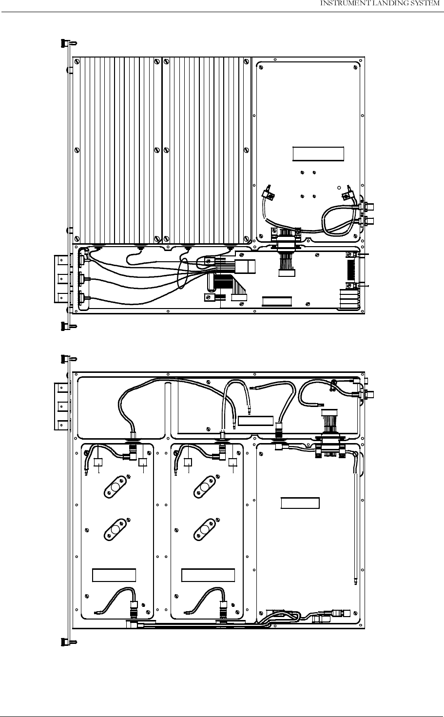
1250$5&7(&+1,&$/+$1'%22.
'(7$,/(''(6&5,37,21 1DYLD$YLDWLRQ$6
Physical Organisation
Figure 9-7 Physical organisation of power amplifier assembly.
FD 1xxxx
PA 123xx *)
PC 1xxxx
CD 123xx *)
AC 1226x
C1 C2 C3 C4
J16
J15
J1
J2
J3
J10J11J12J13
J7
J6
J8
J14
J9
TP1 J17
HBK695-2
PA 123xx
*) Not present in GP-CLR
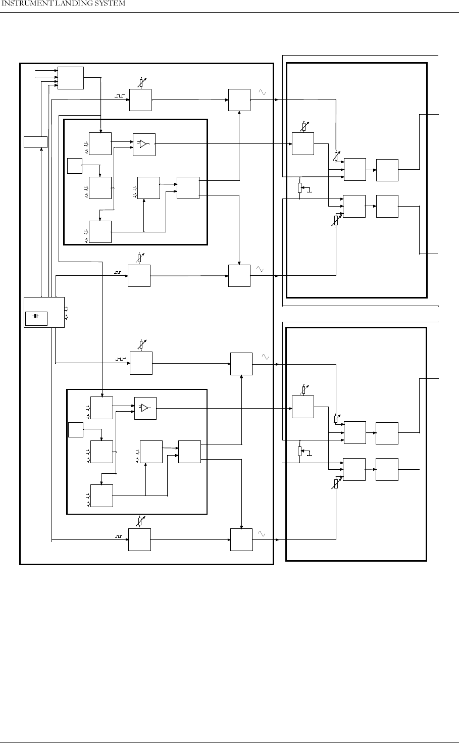
'(7$,/(''(6&5,37,21
1250$5&
7(&+1,&$/+$1'%22.
1DYLD$YLDWLRQ$6
Figure 9-8 NM 7033 Transmitter Block Diagram part 1
VOLT-
AGE
REF.
DATA (7:0)
DATA (7:0)
DATA (7:0)
CONTROL
CONTROL
CONTROL
MOD
LEVEL
RF
LEVEL
DDM
DAC
DIFFER-
ENTIAL
DISTRI-
BUTION
IDENT
KEYER
IDENT + DC LEVEL
MOD 90 LEVEL
MOD 150 LEVEL (DC)
LF_DIG
DATA (7:0)
CONTROL
IDENT/
VOICE
SELECTOR
VOICE
VOICE ON/OFF ANALOGUE IDENT/VOICE
90 Hz
LOWPASS
FILTER
AGC
AMPLIFIER
150 Hz
LOWPASS
FILTER
AGC
AMPLIFIER 150 Hz COU
ANLG_ID
LPF_1020
LP FILTER
MOD_AMP
AGC_AMP2
AGC_AMP
LPF_150
LPF_90
DIGITAL AUDIO
GENERATOR &
CONTROLS
3.6864MHz
Vref
Vref
Vref
Vref
VOLT-
AGE
REF.
DATA (7:0)
DATA (7:0)
DATA (7:0)
CONTROL
CONTROL
CONTROL
MOD
LEVEL
RF
LEVEL
DDM
DAC
DIFFER-
ENTIAL
DISTRI-
BUTION
IDENT
KEYER
IDENT + DC LEVEL
MOD 90 LEVEL
MOD 150 LEVEL
DATA (7:0)
CONTROL
90 Hz
LOWPASS
FILTER
AGC
AMPLIFIER
150 Hz
LOWPASS
FILTER
AGC
AMPLIFIER
90 Hz CLR
150 Hz CLR
MOD_AMP2
AGC_AMP4
AGC_AMP3
LPF_1502
LPF_902
Vref
Vref
Vref
Vref
LF1223A
90 HZ COU
COU
CLR
DAC
DAC
DAC
UNREG 150 Hz
UNREG 90 Hz
UNREG 90 Hz
UNREG 150 Hz
RF BAL
BUFFER
AC1226A
COMPA-
RATOR
AMP_90
MODU-
LATION
CURRENT
DRIVER
AMP_90
MODU-
LATION
CURRENT
DRIVER
AMP_150
COMPA-
RATOR
AMP_150
MOD DEPTH
90 Hz
MOD DEPTH
150Hz
DC
(RF power)
90 Hz FEEDBACK
150 HzFEEDBACK
AC1226A
150 Hz CLR
PHASE ADJ.
90 Hz CLR
PHASE ADJ.
150 Hz COU
PHASE ADJ.
90 Hz COU
PHASE ADJ.
DATA (7:0)
CONTROL
RF BAL
BUFFER
AC1226A
COMPA-
RATOR
AMP_90
MODUL-
ATION
CURRENT
DRIVER
AMP_90
MODUL-
ATION
CURRENT
DRIVER
AMP_150
COMPA-
RATOR
AMP_150
MOD DEPTH
90 Hz
MOD DEPTH
150Hz
DC
(RF power)
90 Hz FEEDBACK
150 HzFEEDBACK
AC1226B
MOD 90 Hz
MOD 150 Hz
150 Hz FEEDBACK
90 Hz FEEDBACK
MOD 90 Hz
MOD 150 Hz
90 Hz FEEDBACK
1
2
3
4
5
6
HBK 750A-1
(RF POWER)
(RF POWER)
1 mm
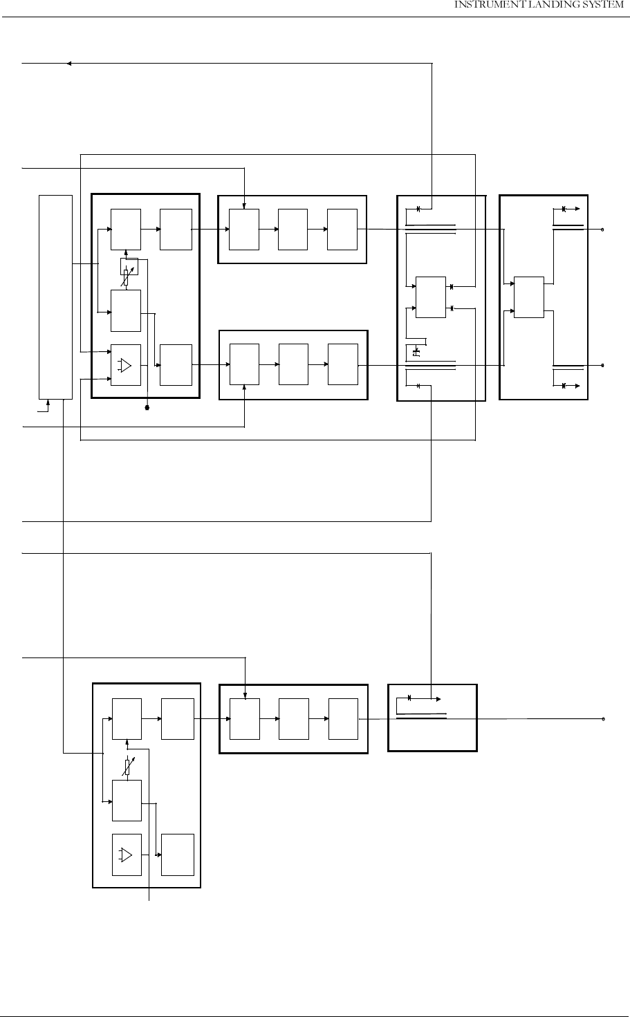
1250$5&7(&+1,&$/+$1'%22.
'(7$,/(''(6&5,37,21 1DYLD$YLDWLRQ$6
Figure 9-9 NM 7033 Transmitter Block Diagram part 2
PC1225B
RF
PHASE
REGU-
LATOR
RF
PHASE
REGU-
LATOR
AMPLIFIER
AMPLIFIER
MODU-
LATOR DRIVER LOWPASS
FILTER
PA1234A
MODU-
LATOR DRIVER LOWPASS
FILTER
PA1234A
90°
HYBRID
RF PHASE ADJ
FD1236A
90°
HYBRID
CSB COU
SBO COU
CD1238A
OS1221B
SYNTHE-
SIZER
Tx ON/OFF
RF PHASE FEEDBACK
RF PHASE FEEDBACK
MODU-
LATOR DRIVER LOWPASS
FILTER
PA1234A
CSB CLR
PHASE
FEEDB.
OFFSET
ADJ.
PHASE OUT
PC1225B
RF
PHASE
REGULATOR
RF
PHASE
REGULATOR
AMPLIFIER
AMPLIFIER
PHASE OUT
PHASE
FEEDB.
OFFSET
ADJ.
FD1224A
1
2
3
4
5
6
HBK 750B-1
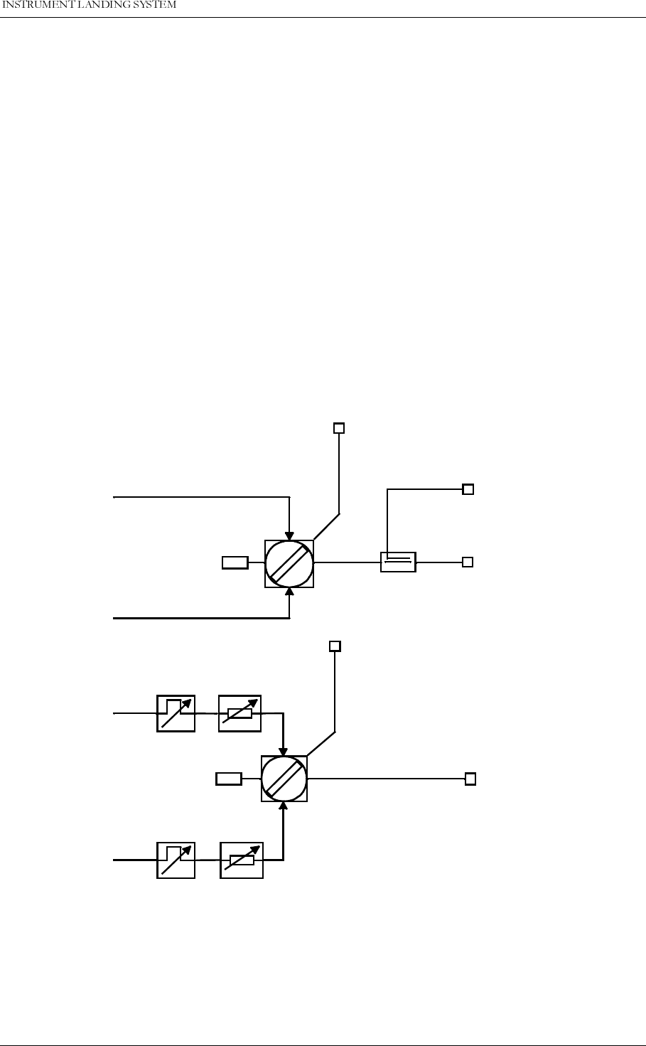
'(7$,/(''(6&5,37,21
1250$5&
7(&+1,&$/+$1'%22.
1DYLD$YLDWLRQ$6
9.1.8 COA1207C Change-Over Assembly
General Description:
The COA1207C consists of one Change-Over Relay Assembly CRA1228A for the Course sig-
nals and one Changeover Relay Unit CR1222A for the Clearance signals.
The Change-Over Assembly for Course utilises two double-throw coaxial relays to connect
the CSB and SBO output signals from either the main or standby transmitter (GPA1231A) to
the antenna system or to a dummy load.
The assembly includes attenuators and phase shifters required to obtain the correct CSB/
SBO relationship.
For the CLR Signal: Only one relay is used as the GP CLR only consists of CSB.
One CRA1228A is shown below. CR1228A contain the CSB circuitry only.
Block Diagram:
Figure 9-10 Changeover system block diagram.
9.1.9 PS1227A Power Supply
General Description:
PHASER ATTENUATOR
COAX
RELAY
COAX
RELAY
OUTPUT
SBO
OUTPUT
CSB
MONITOR
CSB
COUPLER
COAX CONTROL
50 ohm
50 ohm
PHASER ATTENUATOR
COAX CONTROL
CSB
TX1
CSB
TX2
SBO
TX1
SBO
TX2
HBK533-1
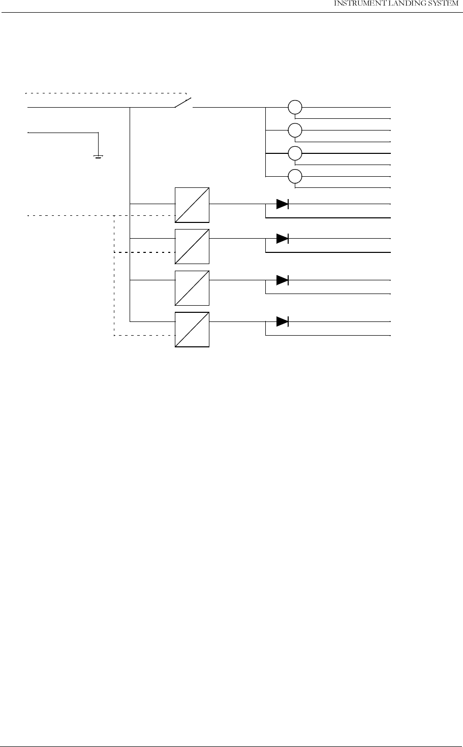
1250$5&7(&+1,&$/+$1'%22.
'(7$,/(''(6&5,37,21 1DYLD$YLDWLRQ$6
PS1227A supplies the NM 70xx cabinet with +27V, ±15V, +8.5V and +5V, from a +27V input.
Block Diagram:
Figure 9-11 PS1227A Block Diagram
Block description:
The ±15V, +8.5V and +5V supplies are provided by integrated DC/DC converter modules.
PS1227A can operate in redundancy with a second power supply using or’ing diodes. The
output voltages are measured prior to these or’ing diodes, to be able to identify a power fail-
ure.
The four 27V outputs supply the GPA1231A power amplifiers. The current drawn are con-
verted to a voltages used for current measurement. The ILS output signals may be shut down
by cutting off the 27V supplies. This is done by the TERMINATOR alarm signal (TRM_AL)
(Ch. 9.1.3.4).
9.1.10 RMA1215A RMS Assembly
General description
The RMA1215A is a microprocessor based assembly that contains the RMS software, and
also forms the basis for the NM7000 RMM system. The RMA1215A consists of KD1214A
front panel with keyboard and display, and the RM1213A the RMS module.
DC
DC
TRM_AL
V27P
GND
A
A
A
A
V27_CL90
V27_CL150
V27_CLR90
V27_CLR150
I27_CL90
I27_CL150
I27_CLR90
I27_CLR150
V15P
V15P_MEAS
V15N
V15N_MEAS
V9P
V9P_MEAS
VDD
VDD_MEAS
SYNC
DC
DC
DC
DC
DC
DC
HBK565-1
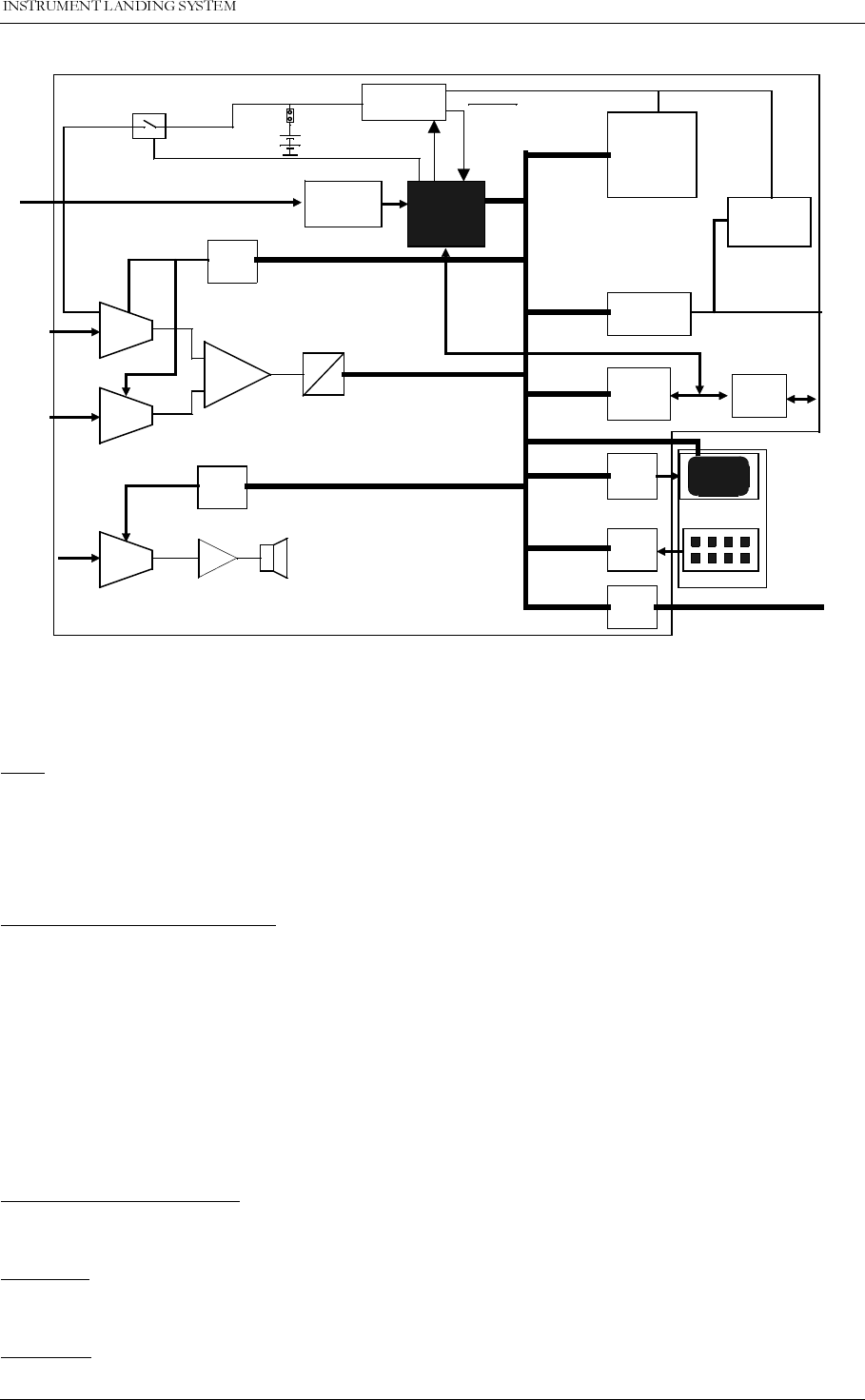
'(7$,/(''(6&5,37,21
1250$5&
7(&+1,&$/+$1'%22.
1DYLD$YLDWLRQ$6
Block Diagram:
Figure 9-12 RMA1215A Block Diagram.
Block description.
CPU
The CPU is an 80C188EB micro controller with address decoding unit and two UARTs. Only
one of these UARTs is utilised for serial communication. The other has been mapped as a par-
allel IO port. The operating frequency of the CPU is 20 MHz provided by an external 40 MHz
oscillator.
WATCHDOG AND BATTERY
A watchdog resets the CPU at power up and if the CPU does not toggle the watchdog reset bit
within app. 1.6 sec. intervals, or if the +5V supply voltage goes below the battery voltage. In
the latter case battery voltage will beconnected to the RAM and RTC. Removal of the battery
or jumper P2 will cause the RESET line to go low and inhibit any function on the module. If a
battery is not available, function can be achieved by shorting the battery socket.The battery
can be disconnected by removing jumper P2 when the module is being stored.The battery
voltage is measured using an opto coupler switch in order not to discharge the battery. The
battery providesapproximately one month memory retention at continuous use (system power
turned off).
INTERRUPT CIRCUITRY
The interrupt circuitry combines several interrupts into the 5 interrupt inputs of the CPU.
DISPLAY
The display used is a 20 characters by 4 lines LCD.
KEYPAD
+
-
Ident
speaker
channels.
IIC bus
Interrupts
Analog
voltages
Det.
ident
Jumper
CPU
CTRL
port
CTRL
port
CTRL
port
RMS bus
Double
UART
CTRL
port
Analog
MUX
Analog
MUX
Analog
MUX
Interrupt
circutry
CTRL
port
AD
Keypad
Display
KD1214A
RM1213A Watchdog
IIC
controller
Battery
RESET
Memory
RAM
EPROM
EEPROM
Real time
clock
RS232
drivers
Three serial
HBK588-1

1250$5&7(&+1,&$/+$1'%22.
'(7$,/(''(6&5,37,21 1DYLD$YLDWLRQ$6
The keypad consists of seven pushbuttons, directly connected to a parallel input port.
DOUBLE UART
The dual UART is a standard UART with a 16 byte bidirectional FIFO on both channels.
RS232 DRIVERS
The RS232 drivers are single supply RS232 drivers. They provide the interface between the
UARTs and external PCs and modems.
IIC CONTROLLER
The IIC controller handles the communication on the IIC bus which is the main communication
ubs for maintenance data collection in the NM 70xx ILS.
REAL TIME CLOCK
The real time clock keeps track of the date and time. Date and time is used to timestamp mon-
itor and maintenance data sets. The RTC accuracy is better than 15 seconds per 24 hours.
CTRL PORT
The CTRL ports in the block diagram are parallel IO ports for the CPU.
ANALOG INTERFACE
The analog interface block contains two analog multiplexers and an A/D-converter. The main
function of this block is to measure analog signals provided from several measurement points
in the NM 70xx equipment. The analog multiplexers are connected to the same address bus
with separate enable bits. This allows the analog inputs to be measured separately as single
ended signals, or to be paired for differential measurements.
AURAL IDENT
The Aural ident block contains an analog MUX, an amplifier and a loudspeaker. It enables the
user to listen to the ident morse code from each of the four transmitters. The Det. ident inputs
are detected CSB signal, filtered through a 1020Hz bandpass filter.
MEMORY
The memory block contains RAM for data storage, EPROM for the program and EEPROM for
permanent system setup parameters. The RAM has battery backup in order to retain logging
data during a power down.
9.1.11 CI1210A External Connection Interface
General Description:
The CI1210A External Connection Interface board provides all the interface for the NM 70xx
equipment for external connections exept from RF signals and power supply.
The module performs transient overload protection on all inputs. In addition CI1210A contains
of a battery protection and a modem demodulation circuit.
The external connections are:
• 1 Remote control port (FSK and opt. RS 232)
• 3 RS232 ports (local and remote RMM)
• 4 DC-loops (antenna cable fault detection)
• 1 DME (keying synchronization)
• 2 Temperature sensors (indoor/outdoor)
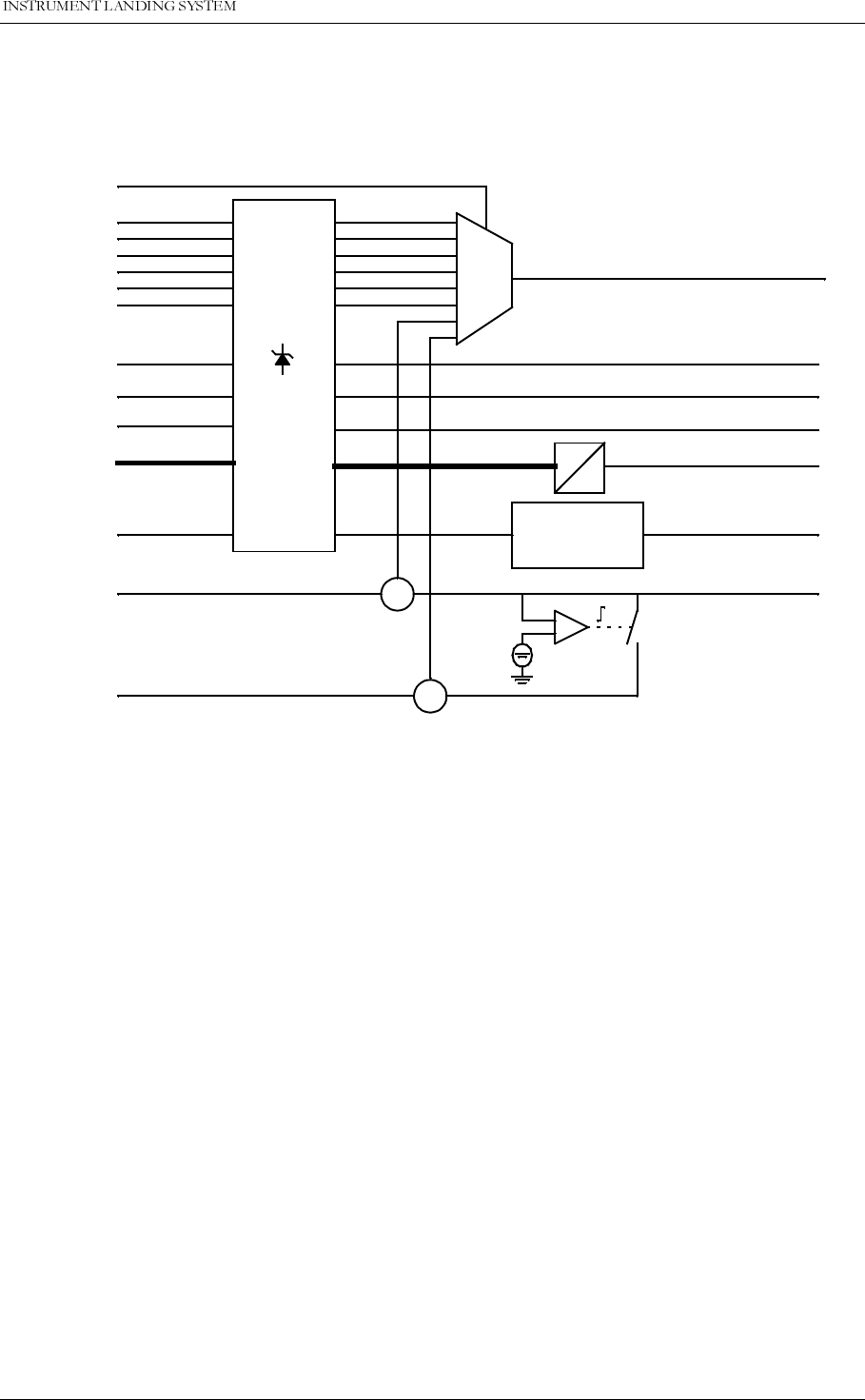
'(7$,/(''(6&5,37,21
1250$5&
7(&+1,&$/+$1'%22.
1DYLD$YLDWLRQ$6
• 1 AC-level measurement input
• 3 Differential Analog inputs
• 8 Auxilliary Digital Inputs/Outputs
Block Diagram:
Figure 9-13 CI1210A Block diagram
9.1.12 MB1203A Monitor Section Motherboard
Description:
MB1203A is the backplane for the 19” subrack in the NM 70xx cabinet. MB 1203A is a passive
motherboard that provides all interconnections between the printed circuit board in this sub-
rack and all interface for external signals exept from RF (Coax) cabling.
+
-
A
A
P
S
Modem
MUX
TOUTDOOR
TINDOOR
VACP/N
ANLG3P/N
ANLG2P/N
ANLG1P/N
EAMX*
AIN*
USER_DIG*
FSK*
SD*,CD
VPOW
VBATT
V27P
IIC*
[RS232]
DL_*
[RS232]
DL_*
Over-
Voltage
Protection
*DME*
DME_*
HBK532-1

1250$5&7(&+1,&$/+$1'%22.
'(7$,/(''(6&5,37,21 1DYLD$YLDWLRQ$6
Table 9-1 MB1203A plug in module connectors.
9.2 Tower Equipment
The following paragraphs describes the modules to be located in the control tower.
9.2.1 RCA1240C Remote Control Assembly
General Description:
The RCA1240C remote control assembly consists of the remote control RC1241A and front
panel RF1242A, and provides the user interface to the ILS Cabinet from the control tower or
technical equipment room. The RCA1240C is connected to the ILS cabinet either using ordi-
nary telephone lines or using the RS232 interface selected by jumper plugs on the RC1241A.
The telephone line interface conforms to V.21 standard (300 baud FSK) for use with ordinary
2-wire 600 ohm telephone line. The transmitter level is -10 dBm, and the receivers dynamic
range is from -10 dBm to -34 dBm.
Most of the functionality of the remote control is provided by the FPGA NMP128A described in
chapter 9.2.1.1.
Section #Module
Monitor 1 1MO 1212A
1MF 1211A
1External Frontend 1
Monitor 2 1MO 1212A
1MF 1211A
1External Frontend 2
Standby Monitor 1MO 1212A
1MF 1211A
Station Control 1TCA 1218A
RMS 1RMA 1215A
Transmitter 1 1LF 1223A
1OS 1221 A/B
Transmitter 2 1LF 1223A
1OS 1221A/B
Power Supply 2PS 1227A
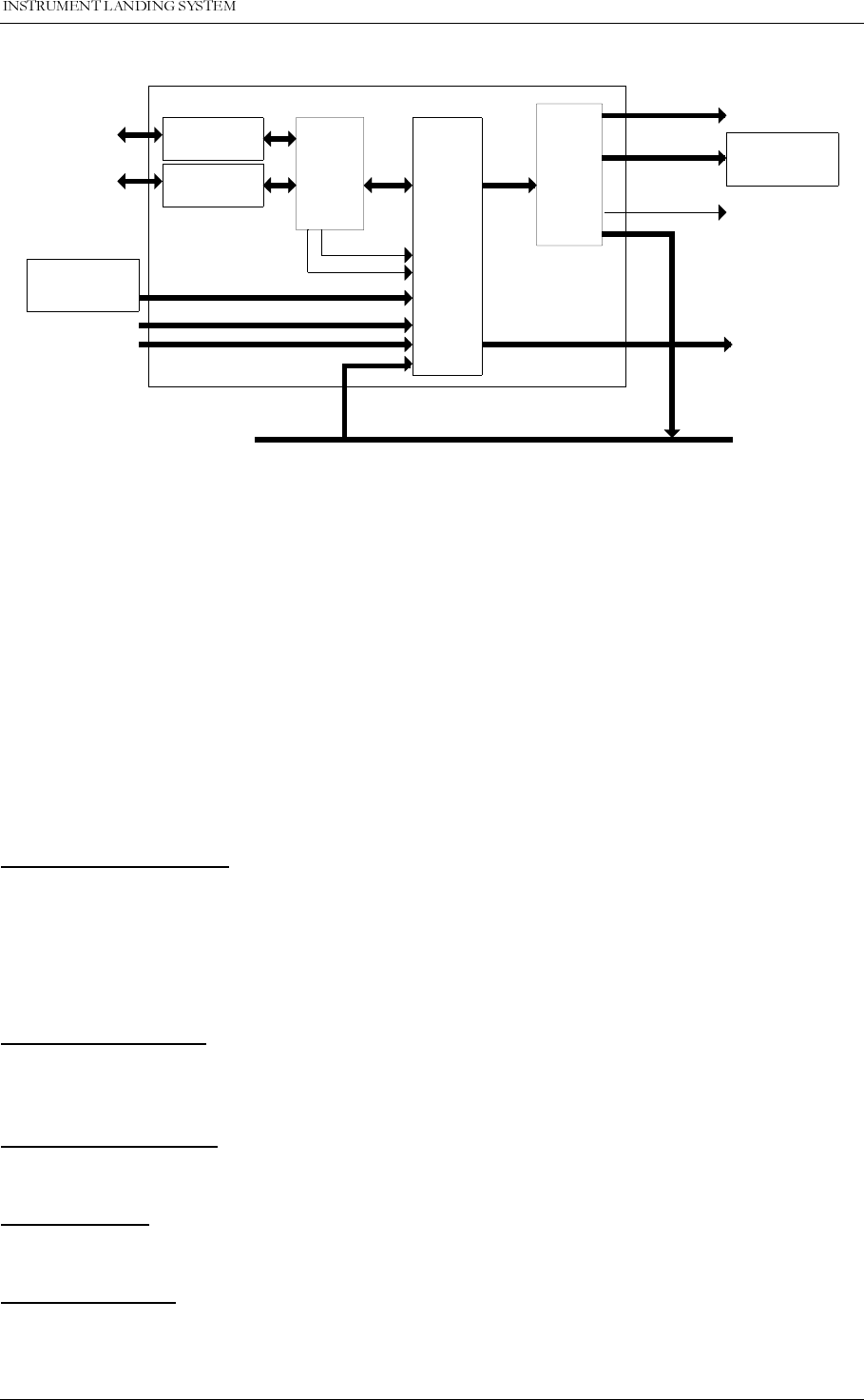
'(7$,/(''(6&5,37,21
1250$5&
7(&+1,&$/+$1'%22.
1DYLD$YLDWLRQ$6
Block Diagram:
Figure 9-14 Block diagram RCA1240C
Block schematic signal description:
Block Description:
CONTROL AND UARTS
This block interprets serial data from the ILScabinet and generates status outputs to front
panel LEDs, slave panel outputs, opto outputs and buzzer signal based on the received sta-
tus. Failure in data from ILS results in alarm condition. Discrete inputs from the front panel
keyboard, control/AUX inputs and slave panel (Ch. 9.2.5) are collected and sent fo the ILS
rack as serial data.
INTERFACE SELECT
These straps selects between telephone line and RS232 for interface with the ILS cabinet.
The default setting is line interface.
LINE DRIVER/MODEM
This block converts logic level serial signals to and from FSK level line signals.
RS232 DRIVER
This block converts logic level serial signals to and from RS232 level signals.
SIGNAL DRIVERS
This block drives the front panel LEDs, opto outputs and slave panel LEDs.
CONTROL INPUTS ILS control signals. Consists of INTERLOCK and TX_OFF.
OPTO OUTPUTS Optocoupler outputs. Collector/emitter for ALARM, NORMAL,
WARNING and STB_ALARM.
SLAVE_DIRECT_BUS Data interface to optional slave panel. Consists of open col-
lector outputs (ALARM, NORMAL, WARNING, STB_ALARM
and SLAVE_BUZZER) and active low inputs (ON_OFF,
CHANGEOVER and SILENCE).
Line
driver/modem
Telephone
line
Control
and
uarts
LED OUTPUTS
RC1241A
RS232
driver
RS232
Signal
drivers
SLAVE DIRECT BUS
RF1242A/B
Front panel
LEDs
AUX_IN AUX_OUT
KEYBOARD INPUTS
RF1242A/B
Keys and
switches
CONTROL INPUTS
SLAVE DIRECT
INPUTS
SLAVE
LED
OUTPUTS
OPTO OUTPUTS
Interface
select
&
config
RST_SL_AURAL_ONLY
STATUS
ALARM
RST_RC_AURAL_ONLY
HBK546-2
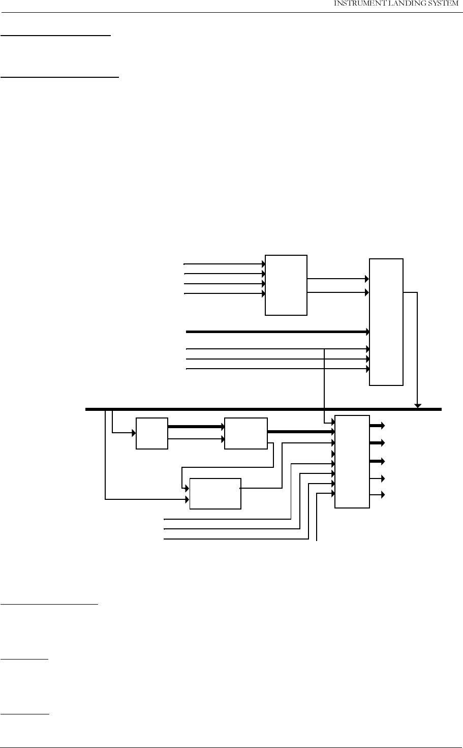
1250$5&7(&+1,&$/+$1'%22.
'(7$,/(''(6&5,37,21 1DYLD$YLDWLRQ$6
FRONT PANEL LEDS
This block contains the front panel LEDs used to indicate the operational status of the ILS.
KEYS AND SWITCHES
This block contains the pushbuttons and switches used for operator input.
9.2.1.1 NMP128A Remote Control
General Description:
NMP128A is a FPGA proiding most of the remote control function. NMP128A is based on the
Actel ACT1020 FPGA. For electrical specifications see the ACT1020 datasheet.
Block Diagram:
Figure 9-15 Block diagram NMP128A
Block Description:
COMMAND MIXER
This block mixes the on/off and changeover commands from the different sources (remote
control front panel or slave front panel input).
TX UART
Converts parallell data to 2-bytes serial messages. The protocol is start bit, 8 data bits, 1 stop
bit, odd parity.
RX UART
Converts serial data from remote control to parallell data (2 bytes).
RX
uart
SERIAL
DATA
IN
New message
timer
Message
detector
LED
&
buzzer
filter
CHANGEOVER_KEY
TX
uart SERIAL
DATA
OUT
AUX_IN
RC_BUS
PARITY ERROR
MESSAGE DATA LED OUTPUTS
NEW MESSAGE
MESSAGE
TIMEOUT
MESSAGE DATA
CARRIER
DETECT SLAVE LEDS
ON_OFF_KEY
SLAVE_ON_OFF_KEY
SLAVE_CHANGEOVER_KEY
Command
mixer
ON_OFF
CHANGEOVER
INTERLOCK
ACCESS_GRANT_SWITCH
TX_OFF
AUX_OUT
ALARM BUZZER
SLAVE BUZZER
SILENCE_KEY
SLAVE_SILENCE_KEY
RST_RC_AURAL_ONLY
564 2

'(7$,/(''(6&5,37,21
1250$5&
7(&+1,&$/+$1'%22.
1DYLD$YLDWLRQ$6
MESSAGE DETECTOR
Messages are accepted only if two equal messages are received in sequence. If so, the data
output is updated and a new-message pulse is asserted.
NEW MESSAGE TIMER
Checks that an OK message and carrier detect is present. Missing message or no carrier
detect for 2 seconds or more gives timeout.
LED & BUZZER FILTER
Data from the ILS cabinet is filtered according to the following descriptions :
• Missing data from ILS sets an alarm condition (Alarm LED on, all other off).
• Activating SILENCE-key turns on all LED’s (lamptest).
• Interlock turns off all LEDs.
Buzzers are activated at transitions from normal to alarm. Lamptest always activates buzzers.
Pressing SILENCE-key deactivates the local buzzer. The remote control SILENCE-key may
deactivate the slave panel buzzer, while SILENCE from the slave panel may deactivate the
local buzzer (both separately configurable).
9.2.2 Motherboard MB1346A
MB1346A is a motherboard for RCA1240C.
Interconnections
J1 Backplane connector for RCA1240C
J2 RS-232 interface for external line modems, radio modems or fibre optic con-
nections (alternative to P9 line connection).
P3 Parallell interface to slave panel or status unit.
P4,P5 Power supply connectors
P6 Aux in/out signals. May be used for FFM status, intruder alarm or other aux-
iliary functions
P7 Opto coupler outputs for ALARM, NORMAL, WARNING and STB. ALARM.
P8 Interlock connector (alternative connector located on slave panel)
P9 RC telephone line interface. Includes alarm output and off input to establish
automatic shutdown of GP when LLZ is off.
NOTE
When MB 1346A is used with RCA 1240C and Interlock function is not used (connected), a
jumper plug must be installed in P8 (or P2 on SF1344A on Slave Panel).
9.2.3 Power Supply PS635B
Description:
PS635B is based on a switch-mode DC/DC converter module (PKA 2212) that features shut-
down at low input voltage and current limiting of outputs ( short circuit proof). Supply inputs
are protected by a fuses.
9.2.4 Motherboard MB1347A
Description:
MB1247A motherboard provides the interface to PS635B power supply (Ch. 9.2.3) through
connectors for 24VDC input and 5VDC output.

1250$5&7(&+1,&$/+$1'%22.
'(7$,/(''(6&5,37,21 1DYLD$YLDWLRQ$6
9.2.5 Slave Panel SF1344A and SP1394A
Description:
The SF1344A and SF1394A slave panel provides user interfaces to the ILS from the control
tower or equipment room. The slave panels are connected to the RCA 1240C remote control
assembly (Ch. 9.2.1) handling the interface with the ILS cabinet. SF 1344A and SF 1394A are
identical apart from mechanical dimensions.
FRONT PANEL LEDS
LEDs on the front panel indicate the ILS status (Alarm/Warning/Normal)
BUZZER
The internal buzzer provides aural alarms.
PUSHBUTTONS
Pushbutton switches provides the on/off and silence (aural alarm reset) function. The silence
button is also used for lamp test.
INTERLOCK CONNECTOR
A connector is provided for interfacing a IL 1379/IL 1380 interlock switch (Ch. 9.2.6).
9.2.6 IL1379 / IL1380 Interlock switch
Description:
The interlock switch is used if the runway has two ILS’s for opposite runway directions that
shall be interlocked.
The interlock switch consists of a key-operated change-over switch, and is connected to the
RCA1240C remote control (Ch. 9.2.1) or SF 1344A/SF1394A slave panels (Ch. 9.2.5) of the
affected localizer and glidepath equipment.
IL 1379 and IL 1380 are identical modules apart from mechanical dimensions. The IL 1379 is
3 height units by 10 length units (app. 12,8x5cm). The IL1380 is 2 height units by 9 length
units (app. 8,4x4,5cm).
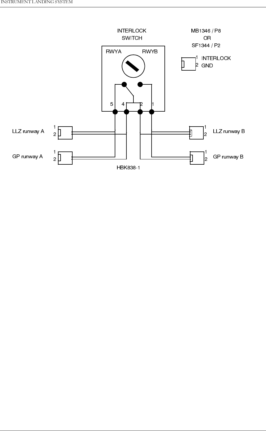


3$576/,676
1250$5&
7(&+1,&$/+$1'%22.
1DYLD$YLDWLRQ$6
10 Parts Lists
10.1 Introduction
This section contains a tabulation of electrical and certain mechanical assemblies and parts;
i.e. chassis-mounted components, circuit cards assemblies, and modules of the equipment to
the lowest replaceable unit (lru).
10.1.1 Explanation of Parts Lists Form
• Symbol/Item No.: References the symbol og item no. for each replaceable electronic part in
the equipment.
• Fig. No.: Lists the figure no of the illustration in which the part is shown.
• Manufactorers Part No.: Navia Aviation part no.
• UOC: Usable on Code: Lists the code assigned to equipment model numbers and identifies
the components used in each model configuration. Se Usable On Code Index.

1250$5&7(&+1,&$/+$1'%22.
3$576/,676 1DYLD$YLDWLRQ$6
10.2 Parts Lists
Electronics Subsystems Group
Symbol/ Fig. Manufactorers Qty./
Item No. No. Description Part No. UOC UOC
NM 7033 10-4 NM 7033 GP CABINET 18884 B -
10-4 GCA 1249A GP 2-FRQ. CAB. ASS. 18523 B -
F1, F2 10-4 CIRCUIT BRAKER 13385 D2
T7 10-4 FUSE 13368 D1
C1 10-4 CAPASITOR 10533 D 1
M2 10-4 COVER PLATE 14874 D2
M1 10-4 FRONT PANEL,TOP 14861 D1
M3 10-4 FRONT PANEL 14837 D1
M4 10-4 COLLAR SCREW 12681 D16
SPL 10-5 POWER SPLITTER 11553 D4
AT1T, AT2T 10-5 ATTENUATOR 11721 D 2
MF 1219A 10-4 MF 1219A GP MONITOR FRONT END 18584 D 2
PS 1227A 10-4 PS 1227A POWER SUPPLY 18615 D 2
OS 1221B 10-4 OS 1221B GP RF-OSCILLATOR 18594 D 2
MO 1212A 10-4 MO 1212A MONITOR 18567 D 2
MB 1203A 10-5 MB 1203A MOTHERBOARD 18540 D 1
TCA 1218 10-4 TCA 1218A TX CONTROL ASSY. 18510 D 1
RMA 1215A 10-4 RMA 1215A RMS ASSY. 18509 D 1
LF 1223A 10-4 LF 1223A LF-GENERATOR 18601 D 2
COA 1207C 10-5 COA 1207C LLZ 2-FRQ. CHANGEOVER ASS. 18508 D -
CRA 1228A 10-5 CRA 1228A LLZ & GP CHANGEOVER R. 18513 D 1
AT1, AT2 10-4 ATTENUATOR 11729 D 2
RL1, RL2 10-5 RELAY 13124 D 2
DL1 10-5 DUMMY LOAD 10602 D 1
DL2 10-5 DUMMY LOAD 10604 D 1
PH 449C 10-4 PH 449C PHASER 16587 D 2
DC 420C 10-5 DC 420C DIRECTIONAL COUPLER 16577 D 2
CR 1222A 10-5 CR 1222A CHANGEOVER RELAYS 18597 D 1
DL1 10-5 DUMMY LOAD 10604 D 1
RL1 10-5 RELAY 13124 D 1
GPA 1231A 10-4 GPA 1231A GP COU POWER AMP. ASSY. 18516 D 2
GPA 1232A 10-4 GPA 1232A GP CLR POWER AMP. ASSY. 18517 D 2
CI 1210A 10-3 CI 1210A CONNECTION INTERFACE BOARD 18561 D 1
F1, F4 10-3 FUSE 13362 C 2
J8, J21, J26 10-3 CONNECTOR 12408 C 3
J9 - J17, J20 10-3 CONNECTOR 12406 C 10
J27-J29 10-3 CONNECTOR 12406 C 3
BC 1361B BATTERY CHARGER 18721 B 1
BATTERY CHARGER 15048 B 2
BATTERY 85Ah 15004 B 2
BATTERY FUSE 14991 B 2
RCA 1240C REMOTE CONTROL 21342 E 1
RC 1241B REMOTE CONTROL 21330 E 1
SKA 1229A SERVICE KIT ASSY. 18514 B -
EB 1349A EXTENSION BOARD 18700 B 1
EB 1245A COAX CABLE EXT. BOARD 18662 B 1
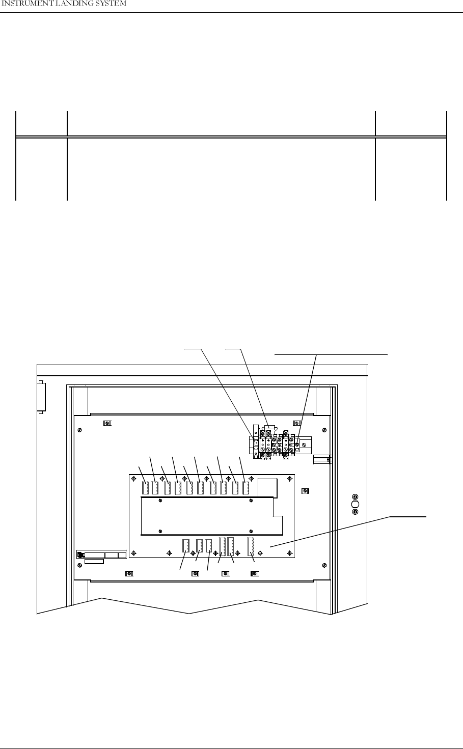
3$576/,676
1250$5&
7(&+1,&$/+$1'%22.
1DYLD$YLDWLRQ$6
10.3 Usable on code index
10.4 Figures
Figure 10-1 Intensionally omitted
Figure 10-2 Intenionally omitted
Figure 10-3 Normarc 7011 & 7033 LLZ & GP cabinet, wall mount side
USABLE ON CODE INDEX
Usable On
Code Description Navia Aviation
Part No.
ANM 7011 LLZ CABINET 18881
BNM 7033 GP CABINET 18884
CLCA 1246A LLZ 2-FRQ. CAB. ASS. 18520
DGCA 1249A GP 2-FRQ. CAB. ASS. 18523
ETOWER EQUIPMENT -
CI 1210A
Terminal block for
power and battery connection
and decoupling capacitor
T07 C01
HBK1148-1
J13
J12
J14
J15
J16 J28
J17 J27
J11
J10
J8
J21
J26
J29
J20
J9
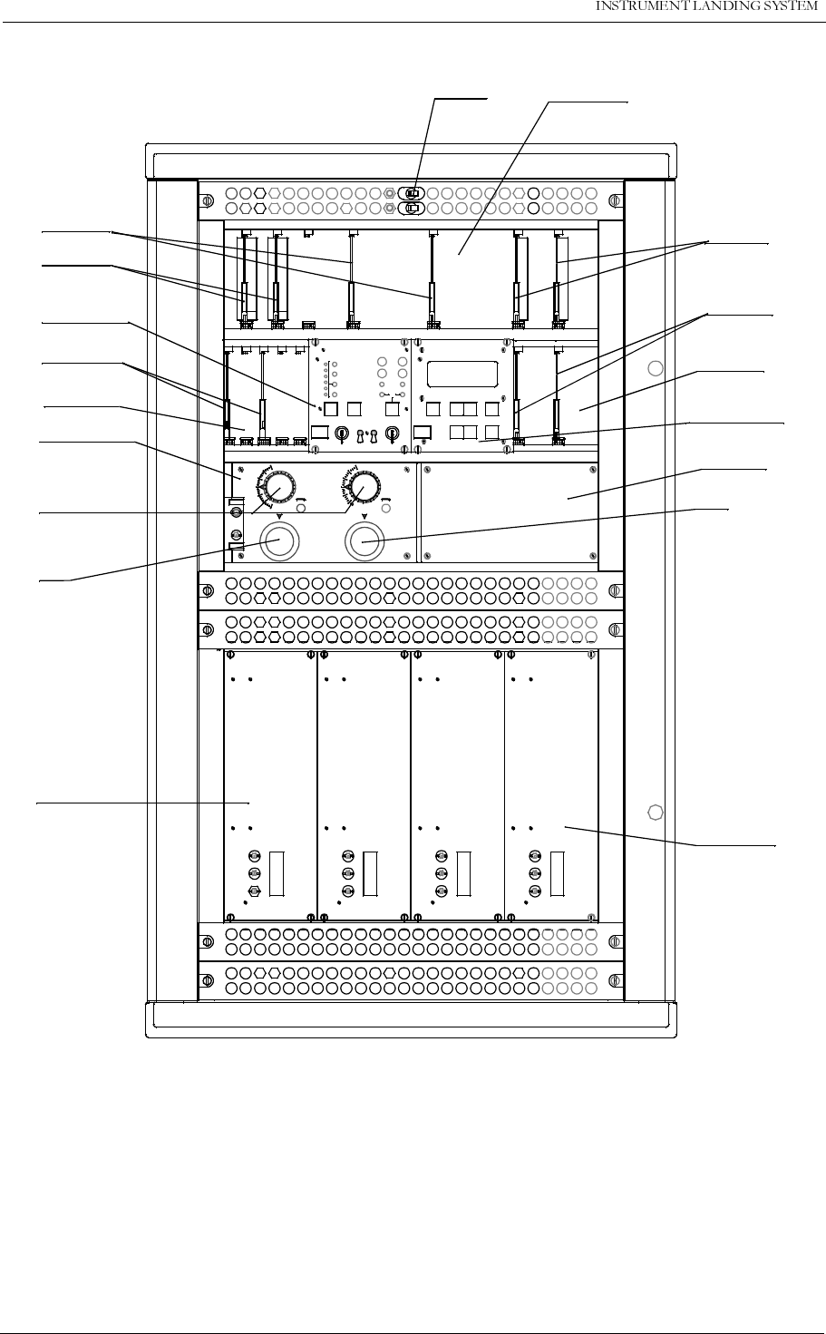
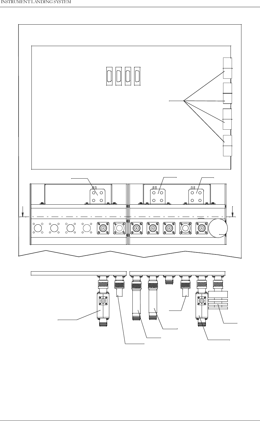
3$576/,676
1250$5&
7(&+1,&$/+$1'%22.
1DYLD$YLDWLRQ$6
Figure 10-5 Normarc 7033 GP cabinet, Rear view
SBO 1
IN IN OUT
SBO 2 SBO
DUMMY OUT
SBO CSB
DUMMY IN
CSB SBO 1
IN OUT
SBO 2 SBO
DUMMY OUT
SBO CSB
DUMMY
CSB
MB 1203
COA 1207C
TX1
CL
TX2
CL
TX1
CLR
TX2
CLR
AA
VIEW A-A
HBK1147-1
DC 420A
DC 420C
DL1CR
AT1T
AT2T
DL2
DL1
CR 1222A CRA 1228A
RL1CR RL2 RL1
SPL


&86720(56,1)250$7,21
1250$5&
$
7(&+1,&$/+$1'%22.
1DYLD$YLDWLRQ$6
WHAT’S YOUR OPINION?
We here in Navia Aviation want to do our utmost to meet the expectations and needs of the
most important people in the world to us - you, our customers.
We will be in contact now and again to make sure you are still satisfied with our products and
our service.
But, please don’t wait for us! Any time you might have a complaint (or compliment) or sugges-
tions as to how we could serve you better, we would appreciate receiving your comments on
the enclosed form - be it about our delivery, product specifications, operation, maintenance,
service, or our performance in general.
We take your opinions seriously, and will confirm receipt of your comments and keep you
advised of any resulting actions.
Yours Sincerely,
Linda Røssland
Customer Service


&86720(56,1)250$7,21
1250$5&
$
7(&+1,&$/+$1'%22.
1DYLD$YLDWLRQ$6
Product Report Please forward to:
Customer Service Dept. CS - No.:
Customer / company: Name: Received by: Date:
Address: Phone: Fax number: E-mail:
Site of installation: Contract number: Navia order No.: Warranty expires:
Product: Serial No:
Fault description / symptoms: Attachement:


&86720(56,1)250$7,21
1250$5&
$
7(&+1,&$/+$1'%22.
1DYLD$YLDWLRQ$6
Customer
Notification of Goods in Transit
Customer’s Engineers to:
Form to be faxed prior to shipment to NAVIA AVIATION AS, Customer Service Dep.
(Fax No. . +47 23 18 02 13)
Sender’s Name:................................................... Tel: .......................................................
Site: ..................................................... Fax: ......................................................
Return Adress:.......................................................................................................................
Consignee:
NAVIA AVIATION AS
P.O. Box 50, Manglerud
N-0612 Oslo Tel: +47 23 18 02 00
NORWAY. Fax: +47 23 18 02 13
Carrier’s Name: ..................................................... Date of Shipment: .............................
Carrier’s Ref No: ................................................... Number of Packages: .............................
The following item(s) will be sent for repair under Maintenance Contract No.
____________
Item Description Quantity Part Number Serial Number
1
2
3
4
5
NAVIA AVIATION AS:
Please fax acknowledgement of goods received (including date received) to:
__________________
