MXCHIP Information Technology EMW3080 Embedded WiFi module User Manual DS0069EN EMW3080 AB V1 1
Shanghai MXCHIP Information Technology Co.,Ltd. Embedded WiFi module DS0069EN EMW3080 AB V1 1
Users Manual

F
F
eatures
Su
p
ARM-C
M
25
6
Wo
r
Ma
x
Mbps w
i
Ma
x
Mbps w
i
E
M
EMW3
0
the secu
r
firmwar
e
accorda
n
E
M
Features
cra
c
ens
u
b
ei
n
sav
e
the
de
v
no
n
dat
a
Wi
-
Datas
p
port 802.11
b
M
4
F
,WLAN
6
KB RAM/ 2
M
r
king Voltag
e
x
imum trans
m
i
th 20 MHz
b
x
imum trans
m
i
th 40 MHz
b
M
W3080B is
s
0
80A has har
d
r
ity level of
C
e
protection.
n
ce with CC
E
M
W3080(A)
H
Encrypt fir
m
c
king
Digital sig
n
u
re integrit
y
n
g tamperin
g
Automatic
a
e
the certifi
c
cloud can
i
v
ice to p
r
e
n
-secure acce
s
Prevent h
a
a
and code
-
Fi Features
Support 80
2
heet
V
b
/g/n, integ
r
MAC
/
Baseb
M
B FLASH
e
: DC 3.0-3.
6
m
ission rate
u
b
andwidth.
m
ission rate
u
b
andwidth.
s
tandard mo
d
d
ware encryp
C
loud conne
c
Security lev
e
E
AL5+ AVA
_
H
ardware Enc
r
m
ware of cl
i
n
ature is use
d
y
and legal
i
g
or replaced
i
a
lly generate
c
ate issued
fr
i
dentify the
e
vent illeg
a
s
sing.
a
ckers to o
b
2
.11b/g/n,
H
E
M
Embed
d
V
ision:1.1
r
ate
and/RF
6
V
u
p to 72.2
u
p to 150
d
ule;
tion. Improv
e
c
tion and
e
l in
_
VAN5
r
yption
i
ents to prev
e
d
in firmware
i
t
y
, prevent
i
i
n OTA.
private key
fr
om the clo
u
legality of
t
a
l, counterf
e
b
tain sensit
i
HT
-40
M
W3080
(
d
ed encrypti
o
Abstr
e
e
nt
to
i
ng
to
u
d,
t
he
e
it,
i
ve
A
M
(
A)/EM
W
o
n security
W
Date:201
7
a
ct
AP
Antenna:
Peri
p
Ope
r
A
pplication
Inte
l
Inte
l
Sma
r
indu
Inte
l
M
odule Type
Typ
e
EMW30
8
EMW30
8
EMW30
8
EMW30
8
W
3080(
B
W
i-Fi modul
7
-02-13
Support Sta
t
Support Eas
y
PCBor IPX
(
p
herals:
2xUART
2x I2C
1x SPI
1x SWD
6x PWM
Up to 13GP
I
r
ating Tempe
l
ligent lighti
n
l
ligent Trans
p
r
t Home Ap
p
strial autom
a
l
ligent Securi
e
8
0(AP) Ha
r
8
0(AE) Har
d
8
0(BP) No
PCB
8
0(BE) No
IPE
X
B
)
e
Num
b
t
ion, Soft A
P
y
Link,Alin
(
Optional)
I
Os
rature:-20
℃
n
g
p
ortation
p
lication
a
tion
ty
Illustratio
n
r
dware Encrypt
d
ware Encrypti
o
Hardware E
Hardware E
X
b
er: DS006
9
P
, Station+So
k,Joinlink
℃
to +85℃
n
ion, PCB
o
n, IPEX
ncryption,
ncryption,
9
CN
ft
H
H
ardware B
l
EM
W
UART x 2
I
2
Cx 2
GPIO x 11
SWD
2MB Flash
PWM x 5
VBAT_MEAS
Copyri
g
M
x
means,
w
l
ock
W
3080(A) Wi-Fi
M
S
O
3
I
n
256KB SRAM
Power M
a
133MHz Co
r
512KB ROM
SPI
EMW
g
ht Notice
x
chip copyri
g
w
ithout the p
r
M
odule Block Di
OC
2.4GHz Radio
3
.3V
n
pu
t
a
nagement
802.11b/g/n
MAC
r
te
x
-M4F MCU
3080(A)
g
hts this spe
c
r
ior written c
o
agram
U.F.L connector
On-board
PCB Ant
40MHz
OSC
Encryption
Chip
c
ification. N
o
o
nsent of M
x
o
part of thi
x
chip.
s specificati
o
EWM3080
(
o
n may be r
e
(
B)
eproduced i
n
n
any form
o
o
r

MXCHIP All Rights Reserved
无法显示图像。计算机可能没有足够的内存以打开该图像,也可能是该图像已损坏。请重新启动计算机,然后重新打开该文件。如果仍然显示红色“x”,则可能需要删除该图像,然后重新将其插入。
Datasheet [Page 1]
EMW3080
Vision Illustration
Date Vision Details
2017-01-16 1.0 Initial document
2017-02-13 1.1
Update label, package, RF reference, encryption. Add
BOOT/EASYLINK description

MXCHIP All Rights Reserved
无法显示图像。计算机可能没有足够的内存以打开该图像,也可能是该图像已损坏。请重新启动计算机,然后重新打开该文件。如果仍然显示红色“x”,则可能需要删除该图像,然后重新将其插入。
Datasheet [Page 2]
EMW3080
Content
Abstract ................................................................................................................................................................................. 1
Vision Illustration ................................................................................................................................................................. 1
1. Product Introduction ..................................................................................................................................................... 4
1.1 EMW3080 LABEL INFORMATION ..................................................................................................................... 5
1.2 PIN ARRANGEMENT .......................................................................................................................................... 6
1.3 PIN DEFINITION ................................................................................................................................................ 8
1.3.1 EMW3080 Package Definition ............................................................................................................ 8
1.3.2 EMW3080 Pin Definition.................................................................................................................... 8
2. Electrical Parameters .................................................................................................................................................. 10
2.1 OPERATING CONDITIONS ................................................................................................................................ 10
2.2 POWER PARAMETERS ...................................................................................................................................... 10
2.3 WORKING ENVIRONMENT ............................................................................................................................... 11
2.4 ELECTROSTATIC DISCHARGE .......................................................................................................................... 11
3. RF parameters ............................................................................................................................................................. 12
3.1 BASIC RF PARAMETERS .................................................................................................................................. 12
3.2 TX PERFORMANCE ......................................................................................................... 错误!未定义书签。
3.2.1 Transmit performance of IEEE802.11b mode ................................................... 错误!未定义书签。
3.2.2 Transmit performance of IEEE802.11g mode ................................................... 错误!未定义书签。
3.2.3 Transmit performance of IEEE802.11n-HT20 mode......................................... 错误!未定义书签。
3.3 RX RECEIVE SENSITIVITY .............................................................................................................................. 12
3.3.1 IEEE802.11b Mode ........................................................................................................................... 12
3.3.2 IEEE802.11g Mode ........................................................................................................................... 13
3.3.3 IEEE802.11n-HT Mode ..................................................................................................................... 13
4. Antenna Information ................................................................................................................................................... 15
4.1 ANTENNA TYPE .............................................................................................................................................. 15
4.2 PCB ANTENNA CLEARANCE ZONE ................................................................................................................. 15
4.3 EXTERNAL ANTENNA CONNECTOR ................................................................................................................. 17
5. Assembly Information and Production Guidance ....................................................................................................... 18
5.1 ASSEMBLY SIZE .............................................................................................................................................. 18
5.2 PRODUCTION GUIDANCE(IMPORTANT) ...................................................................................................... 19
5.3 CONSIDERATIONS ............................................................................................................................................ 20
5.4 STORAGE CONDITION ..................................................................................................................................... 21
5.5 TEMPERATURE CURVE OF SECONDARY REFLOW ............................................................................................. 22
6. Reference Circuit ........................................................................................................................................................ 23
7. Module MOQ and Package Information ..................................................................................................................... 25
8. Sales Information and Technical Support ................................................................................................................... 26
Figure Content
Figure 1 EMW3080 Label Information ............................................................................................................... 6

MXCHIP All Rights Reserved
无法显示图像。计算机可能没有足够的内存以打开该图像,也可能是该图像已损坏。请重新启动计算机,然后重新打开该文件。如果仍然显示红色“x”,则可能需要删除该图像,然后重新将其插入。
Datasheet [Page 3]
EMW3080
Figure 2 DIP Package Size ............................................................................................................................... 7
Figure 3 LGA Package Size .............................................................................................................................. 7
Figure 4EMW3080 Package Definition .............................................................................................................. 8
Figure 5Minimum Clearance Zone of PCB Antenna (Unit: mm) ..................................................................... 16
Figure 6 Size of External Antenna Connector ................................................................................................... 17
Figure 7 EMW3080Side View (Unit: mm) ........................................................................................................ 18
Figure 8 Humidity Card ..................................................................................................................................... 19
Figure 9 Storage Condition ................................................................................................................................ 21
Figure 10 Temperature Curve of Secondary Reflow ......................................................................................... 22
Figure 11 Power Source Circuit ......................................................................................................................... 23
Figure 12USB to UART .................................................................................................................................... 23
Figure 13External Interface Circuit of EMW3080 ............................................................................................ 24
Figure 14 3.3V UART- 5V UART Convert Circuit ........................................................................................... 24
Table Content
Table 1 EMW3080 Pin Definition ....................................................................................................................... 8
Table 2 Range of input voltage .......................................................................................................................... 10
Table 3Absolute maximum voltage rating ......................................................................................................... 10
Table 4EMW3080 2.2Power Parameters ..................................................................................................... 10
Table 5Temperature and humidity condition ...................................................................................................... 11
Table 6 Electrostatic Discharge Parameters ........................................................................................................ 11
Table 7Radio-frequency standards ..................................................................................................................... 12
Table 8CCK_11 transmit performance parameters of IEEE802.11b mode ....................... 错误!未定义书签。
Table 9OFDM_54 transmit performance parameters of IEEE802.11g mode .................... 错误!未定义书签。
Table 10MCS7 transmit performance parameters of IEEE802.11n-HT20 mode .............. 错误!未定义书签。
Table 11 MCS7 Transmit Performance of IEEE802.11n-HT 40MHz mode ..................... 错误!未定义书签。
Table 12Receive Sensitivity of IEEE802.11b Mode with Bandwidth 20MHz(dBm) ........................................ 12
Table 13 Receive Sensitivity of IEEE802.11g Mode with Bandwidth 20MHz(dBm) ....................................... 13
Table 14 Receive Sensitivity of IEEE802.11n-HT20 Mode with Bandwidth 20MHz(dBm) ............................ 13
Table 15 Receive Sensitivity of IEEE802.11n-HT40 Mode (dBm) ................................................................... 14
MXCHIP All Rights Reserved
无法显示图像。计算机可能没有足够的内存以打开该图像,也可能是该图像已损坏。请重新启动计算机,然后重新打开该文件。如果仍然显示红色“x”,则可能需要删除该图像,然后重新将其插入。
Datasheet [Page 4]
EMW3080
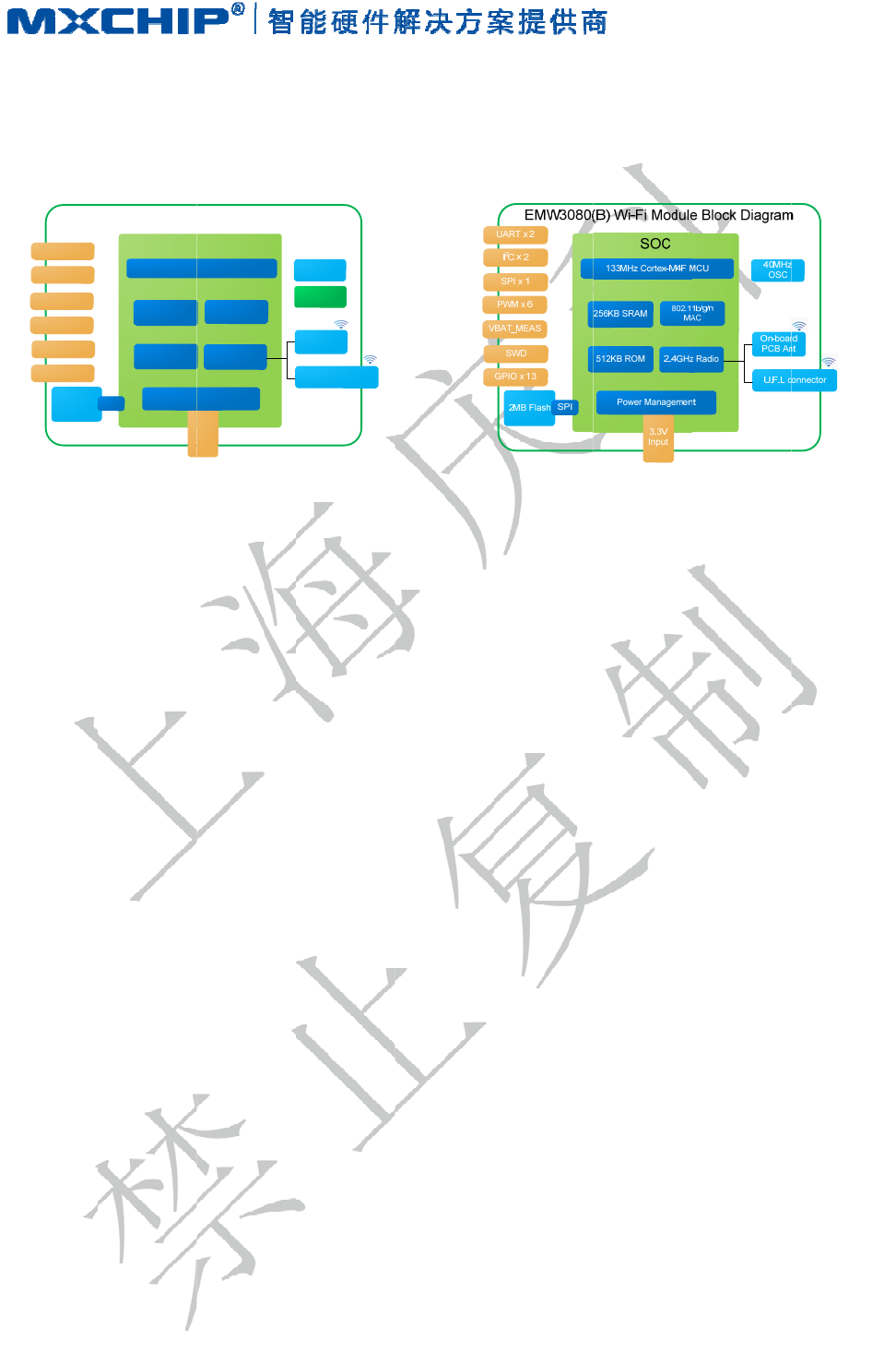
1. Product Introduction
EMW3080 is a cost-effective embedded Wi-Fi module released by MXCHIP with high integrating ARM
CM4F, WLAN MAC/Baseband/RF. Maximum frequency 133MHz with 256KB SRAM and 2M FLASH. Power
supply is DC 3.3V. Installation modes are LGA SMT and Pin Connection. Peripheral: 2xUART / 1x SPI /2x I2C /
6x PWM / Up to 13 GPIOs.
EMW3080 operates MiCO 3.0 IoT operating system, supporting Micoder 1.0 development system. Provide
fast, stable and secure end-to-end cloud links to users with integrate TCP/IP protocol stack, various security
encryption algorithm, intelligent cloud such as MXCHIP easylink/Alink 1.1/Joinlink 3.0/Hilink/One
Net/Gome/Suning, oversea cloud such as AWS/Ayla/Azure/IBM Watson/Google/Apple Homekit.
EMW3080 (A): Provide securityencryption chip to the integrity and legality and cloud communication safety
of client firmware.
EMW3080 (B): Abundant peripherals and memory to supply most application and multi-cloud requirement.
Hardware diagram is shown below with four main parts:
CM4F main core
WLAN MAC/BB/RF/ANT
Hardware encryption
Power management
With:
1. ARM CM4FCPU with 133MHz maximum frequency and 256KB SRAM and 2M FLASH. Support high
speed UART, I2C, SPI, PWM and multi-GPIO.
2. 2MB SPI Flash is used for custom firmware development
3. Support PCB antenna and IPEX
4. Input voltage:DC 3.3V
EMW3080(A) Wi-Fi Module Block Diagram
SOC
2.4GHz Radio
U.F.L connector
On-board
PCB Ant
3.3V
Input
40MHz
OSC
256KB SRAM
UART x 2
I2Cx 2
GPIO x 11
Power Management
802.11b/g/n
MAC
133MHz Cortex-M4F MCU
512KB ROM
SWD
2MB Flash SPI
PWM x 5 Encryption
Chip
VBAT_MEAS
EMW3080 Hardware block
MXCHIP All Rights Reserved
无法显示图像。计算机可能没有足够的内存以打开该图像,也可能是该图像已损坏。请重新启动计算机,然后重新打开该文件。如果仍然显示红色“x”,则可能需要删除该图像,然后重新将其插入。
Datasheet [Page 5]
EMW3080
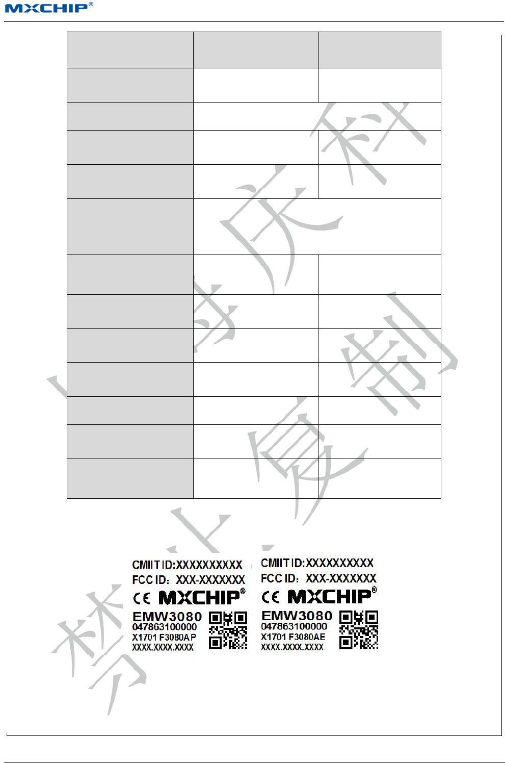
1.1 EMW3080 Label Information
EMW3080(A) EMW3080(B)
Encryption security chip Inside External support
CPU ARM CM4F
CPU Maximum Speed 133MHz 133MHz
SRAM 256KB 256KB
Flash(QSPI
100MHz) 2MB(Support XIP CACHE running and decrypting)
UART (Maximum
6Mbps) 2 2
I2C (400KHz) 2 2
SPI (31.25MHz) None 1
PWM (Maximum 4MHz) 5 6
SWD debug port 1 1
Debug port 1 1
GPIO(Output current
4mA) 11 13

MXCHIP All Rights Reserved
无法显示图像。计算机可能没有足够的内存以打开该图像,也可能是该图像已损坏。请重新启动计算机,然后重新打开该文件。如果仍然显示红色“x”,则可能需要删除该图像,然后重新将其插入。
Datasheet [Page 6]
EMW3080
Figure1EMW3080 Label Information
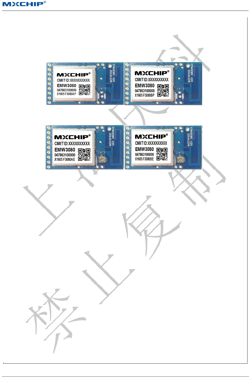
Label Information:
CMIIT ID:XXXXXXXX : SRRC approval number
FCC ID:XXX-XXXXXXX :FCC certification information
CE: CE authenticationlog
EMW3080: Module type
047863100000:MAC address(Each module has a unique MAC address)
F3080AP /F3080AE: Sub model type of module A, PCB antenna or IPEX
F3080BP /F3080BE: Sub model type of module B, PCB antenna or IPEX
X1701:production batch
XXXX.XXXX.XXXX : SN series number
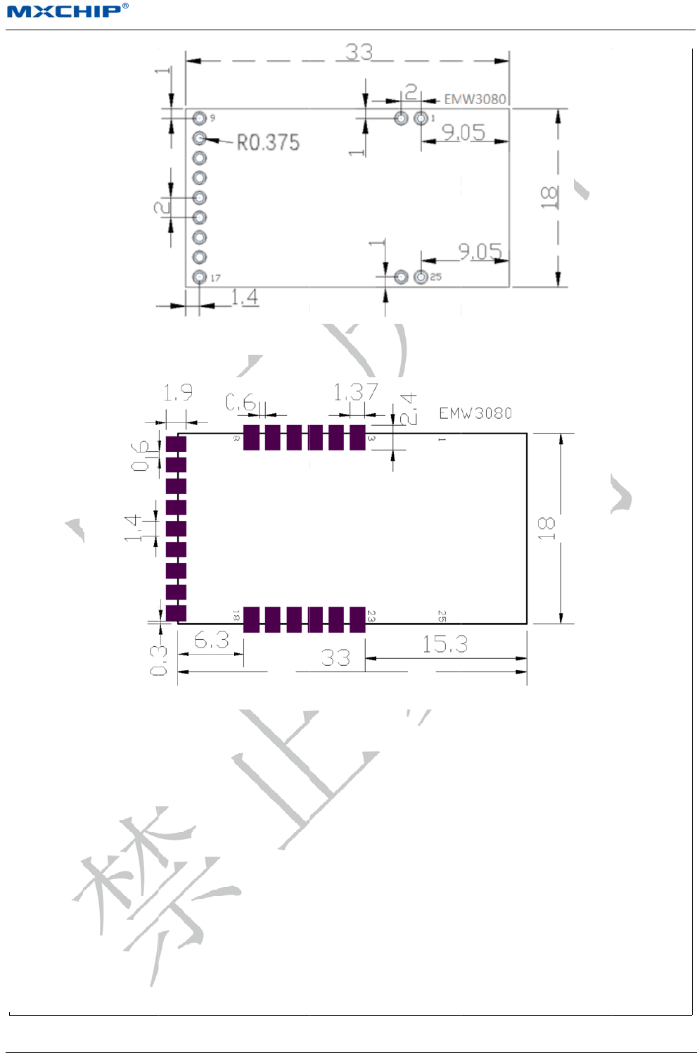
1.2 Pin Arrangement
EMW3080 has LGA package and DIP package, DIP package (as shown in figure 2) could effectively reduce
the quality risk of second patch;LGA package (as shown in figure 3) is easy to debug, provide multi-choice for
customers.
Solder mask openness has the same size with land. The width of steel mesh is suggested to be 0.12mm to
0.14mm in SMT.
无法显示图像。计算机可能没有足够的内存以打开该图像,也可能是该图像已损坏。请重新启动计算机,然后重新打开该文件。如果仍然显示红色“x”,则可能需要删除该图
像
,然后重新将其插入。
Fig
u
Figur
e
MXCHIP All Rights Reserved
Datasheet
EMW3080
u
re2DIP Pac
k
e
3 LGA Pa
c
k
age Size
c
kage Size
[Page 7]
MXCHIP All Rights Reserved
无法显示图像。计算机可能没有足够的内存以打开该图像,也可能是该图像已损坏。请重新启动计算机,然后重新打开该文件。如果仍然显示红色“x”,则可能需要删除该图像,然后重新将其插入。
Datasheet [Page 8]
EMW3080
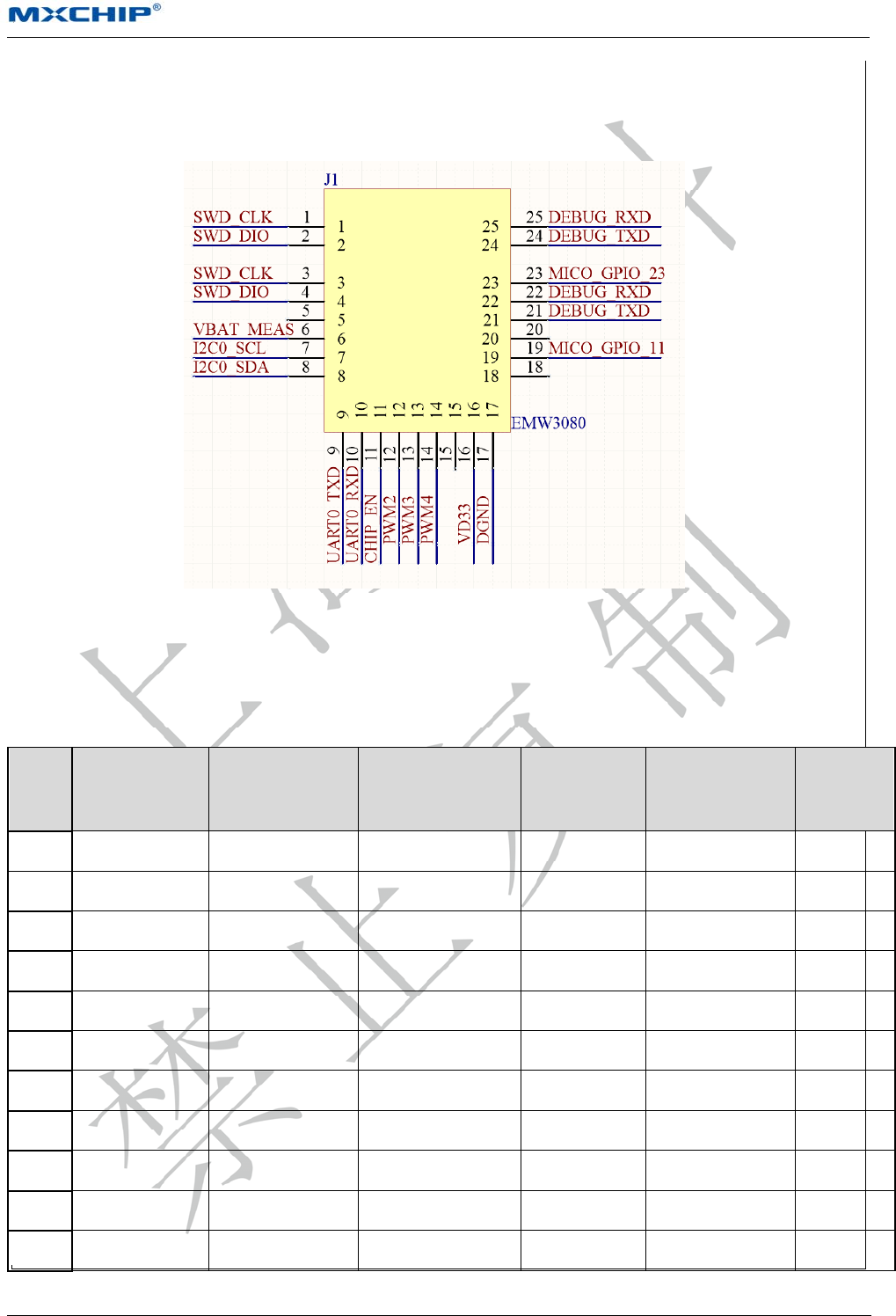
1.3 Pin Definition
1.3.1 EMW3080Package Definition
Figure4EMW3080 Package Definition
1.3.2 EMW3080 Pin Definition
Table1EMW3080 Pin Definition
Pin
numb
er
FUNCTION1 FUNCTION2 FUNCTION3 FUNCTION4 FUNCTION5 FUNCTION6
1, 3 MICO_GPIO_1 MICO_PWM1 SWCLK
2, 4 MICO_GPIO_2 MICO_PWM2 SWDIO
5 NC
6 VBAT MEAS
7 MICO_GPIO_7 MICO_I2C0_SCL MICO_UART0_RTS MICO_PWM6 MICO_SPI1_MISO
8 MICO_GPIO_8 MICO_I2C0_SDA MICO_UART0_CTS MICO_SPI1_CS
9 MICO_GPIO_9 MICO_I2C1_SDA MICO_UART0_TXD MICO_PWM1 MICO_SPI1_MOSI
10 MICO_GPIO_10 MICO_I2C1_CLK MICO_UART0_RXD MICO_SPI1_CLK
11 CHIP_EN
12 MICO_GPIO_12 MICO_PWM3
13 MICO_GPIO_13 MICO_PWM4
MXCHIP All Rights Reserved
无法显示图像。计算机可能没有足够的内存以打开该图像,也可能是该图像已损坏。请重新启动计算机,然后重新打开该文件。如果仍然显示红色“x”,则可能需要删除该图像,然后重新将其插入。
Datasheet [Page 9]
EMW3080
14 MICO_GPIO_14 MICO_PWM5
15 NC
16 VDD
17 GND
18 NC
19 MICO_GPIO_19
20 NC
21, 24 MICO_GPIO_21 MICO_I2C0_SDA MICO_UART1_TXD MICO_PWM4
22, 25 MICO_GPIO_22 MICO_I2C0_SCL MICO_UART1_RXD MICO_PWM5
23 MICO_GPIO_23
Illustration:words in black color is the common pins in both A and B, words in blue color is unique pins of
B module. Compare to A module, EMW3080(B) has four pins: PIN 7,8,9,10 with function: traffic control of
UART, SPI function,PWM output and GPIO.
PIN 19 is used as BOOT,PIN23 is used as EASYLINK, please do not use pin 19 and 23 in hardware 硬件
design. Please contact engineer of MXCHIP if it is necessary to use the two pins.
PIN21/24should be in high voltage or NC when power on,please aware it when designing circuit.
CHIP_EN could not be set NC, the other pins should not be set NC.
MXCHIP All Rights Reserved
无法显示图像。计算机可能没有足够的内存以打开该图像,也可能是该图像已损坏。请重新启动计算机,然后重新打开该文件。如果仍然显示红色“x”,则可能需要删除该图像,然后重新将其插入。
Datasheet [Page 10]
EMW3080
2. Electrical Parameters
2.1 Operating Conditions
EMW3080would be unstable when input voltage is less than the lowest rated voltage.
Table2Range of input voltage
Symbol Illustration Condition
Details
Minimum Typ Maximum Unit
VDD Power Supply 3.0 3.3 3.6 V
There would be permanent damage in hardware if the device operates at the voltage over rated value.
Meanwhile, reliability could be influenced when the device has a long-term operating at maximum voltage.
Table3Absolute maximum voltage rating
Symbol Description Minimum Typ Unit
VDD Module input voltage –0.3 3.6 V
VIN GPIO input voltage −0.3 3.6 V
2.2 Power Parameters
Table4EMW3080 2.2 Power Parameters
Status Current(3V3) Description
WIFIInitialization 26.91mA
Enable WIFI, low power consumption
Connect WIFI 47.71mA Enable WIFI,low power consumption
UDPtransmission 168.37mA Disable WIF, low power consumption
SoftAP 121.48mA
SoftAPconnect to internet
Easylink 122.84mA
Process of module network distribution
Standby 10.45uA Ultra low standby power mode
Actual working current is variable at different operating mode. Maximum operating current 300 mA 。
MXCHIP All Rights Reserved
无法显示图像。计算机可能没有足够的内存以打开该图像,也可能是该图像已损坏。请重新启动计算机,然后重新打开该文件。如果仍然显示红色“x”,则可能需要删除该图像,然后重新将其插入。
Datasheet [Page 11]
EMW3080
2.3 Working Environment
Table5Temperature and humidity condition
Symbol Name Maximum Unit
TSTG Storage Temperature -55 to +125
℃
TA Operation Temperature -20 to +85
℃
Humidity Non-condensing, Relative humidity 95 %
2.4 Electrostatic Discharge
Table6Electrostatic Discharge Parameters
Symbol Name Details Level Maximum Unit
VESD(HBM)
Electrostatic discharge
voltage
(Human module)
TA= +25 °C , JESD22-A114 2 2000
V
VESD(CDM)
Electrostatic discharge
voltage
(Discharge device
module)
TA = +25 °C , JESD22-C101 II 500
MXCHIP All Rights Reserved
无法显示图像。计算机可能没有足够的内存以打开该图像,也可能是该图像已损坏。请重新启动计算机,然后重新打开该文件。如果仍然显示红色“x”,则可能需要删除该图像,然后重新将其插入。
Datasheet [Page 12]
EMW3080
3. RF parameters
3.1 Basic RF parameters
Table7Radio-frequency standards
Name Illustration
Working frequency 2.412~2.484GHz
Wi-Fi wireless standard IEEE802.11b/g/n20/n40
Maximum output power 18dBm
Data
transmission rate
20MHz
11b:1,2,5.5,11Mbps
11g:6,9,12,18,24,36,48,54Mbps
11n: MCS0~7,72.2Mbps
40MHz 11n:MCS0~7,150Mbps
Antenna type PCB(Default)
IPX (Optional)
3.2 RX Receive Sensitivity
3.2.1 IEEE802.11b Mode
Table8Receive Sensitivity of IEEE802.11b Mode with Bandwidth 20MHz(dBm)
Rate
Channel 11M 1M
IEEE spec -76dBm -83dBm
1 -90dBm -100dBm
2 -90dBm -100dBm
3 -90dBm -100dBm
4 -90dBm -100dBm
5 -90dBm -100dBm
6 -90dBm -100dBm
7 -90dBm -100dBm
8 -90dBm -100dBm
9 -90dBm -100dBm
10 -90dBm -100dBm
11 -90dBm -100dBm
12 -90dBm -100dBm
MXCHIP All Rights Reserved
无法显示图像。计算机可能没有足够的内存以打开该图像,也可能是该图像已损坏。请重新启动计算机,然后重新打开该文件。如果仍然显示红色“x”,则可能需要删除该图像,然后重新将其插入。
Datasheet [Page 13]
EMW3080
Rate
Channel 11M 1M
13 -90dBm -100dBm
3.2.2 IEEE802.11g Mode
Table9Receive Sensitivity of IEEE802.11g Mode with Bandwidth 20MHz(dBm)
Rate
Channel
54M 6M
IEEE spec -65dBm -82dBm
1 -76dBm -92dBm
2 -76dBm -92dBm
3 -76dBm -92dBm
4 -76dBm -92dBm
5 -76dBm -92dBm
6 -76dBm -92dBm
7 -76dBm -92dBm
8 -76dBm -92dBm
9 -76dBm -92dBm
10 -76dBm -92dBm
11 -76dBm -92dBm
12 -76dBm -92dBm
13 -76dBm -92dBm
3.2.3 IEEE802.11n-HT Mode
Table10Receive Sensitivity of IEEE802.11n-HT20 Mode with Bandwidth 20MHz(dBm)
Channel Rate MCS7 MCS0
IEEE spec -64dBm -82dBm
1 -73dBm -92dBm
2 -73dBm -92dBm
3 -73dBm -92dBm
4 -73dBm -92dBm
5 -73dBm -92dBm
6 -73dBm -92dBm
7 -73dBm -92dBm
MXCHIP All Rights Reserved
无法显示图像。计算机可能没有足够的内存以打开该图像,也可能是该图像已损坏。请重新启动计算机,然后重新打开该文件。如果仍然显示红色“x”,则可能需要删除该图像,然后重新将其插入。
Datasheet [Page 14]
EMW3080
Channel Rate MCS7 MCS0
8 -73dBm -92dBm
9 -73dBm -92dBm
10 -73dBm -92dBm
11 -73dBm -92dBm
12 -73dBm -92dBm
13 -73dBm -92dBm
Table11Receive Sensitivity of IEEE802.11n-HT40 Mode(dBm)
Rate
Channel
MCS7 MCS0
IEEE spec -64dBm -82dBm
3 -69dBm -89dBm
4 -69dBm -89dBm
5 -69dBm -89dBm
6 -69dBm -89dBm
7 -69dBm -89dBm
8 -69dBm -89dBm
9 -69dBm -89dBm
10 -69dBm -89dBm
11 -69dBm -89dBm
MXCHIP All Rights Reserved
无法显示图像。计算机可能没有足够的内存以打开该图像,也可能是该图像已损坏。请重新启动计算机,然后重新打开该文件。如果仍然显示红色“x”,则可能需要删除该图像,然后重新将其插入。
Datasheet [Page 15]
EMW3080
4. Antenna Information
4.1 Antenna Type
EMW3080has two type of antenna: EMW3080(AP/BP) and EMW3080(AE/BE)
EWM3080(AP) EMW3080(BP)
EMW3080(AE) EMW3080(BE)
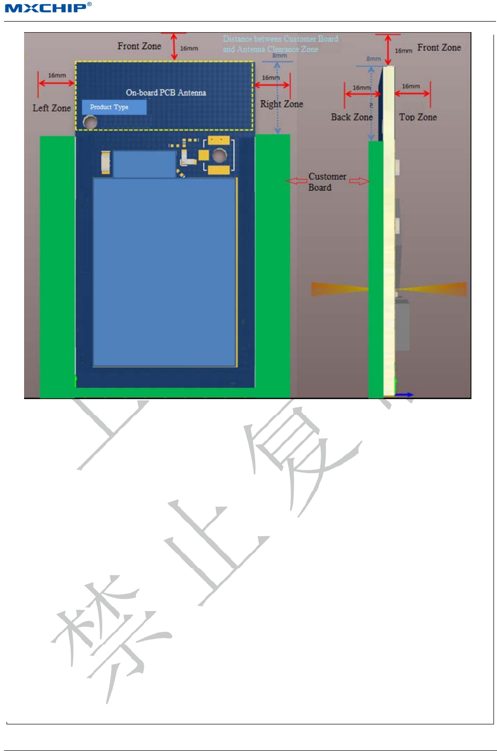
4.2 PCB Antenna Clearance Zone
Main PCB should have a distance over 16mm with other metal elements when using PCB antenna in Wi-Fi
device. Shadow parts in the figure below should keep away from metal elements, sensor, interference source and
other material that could cause signal interference.
MXCHIP All Rights Reserved
无法显示图像。计算机可能没有足够的内存以打开该图像,也可能是该图像已损坏。请重新启动计算机,然后重新打开该文件。如果仍然显示红色“x”,则可能需要删除该图像,然后重新将其插入。
Datasheet [Page 16]
EMW3080
Figure5Minimum Clearance Zone of PCB Antenna (Unit: mm)
MXCHIP All Rights Reserved
无法显示图像。计算机可能没有足够的内存以打开该图像,也可能是该图像已损坏。请重新启动计算机,然后重新打开该文件。如果仍然显示红色“x”,则可能需要删除该图像,然后重新将其插入。
Datasheet [Page 17]
EMW3080
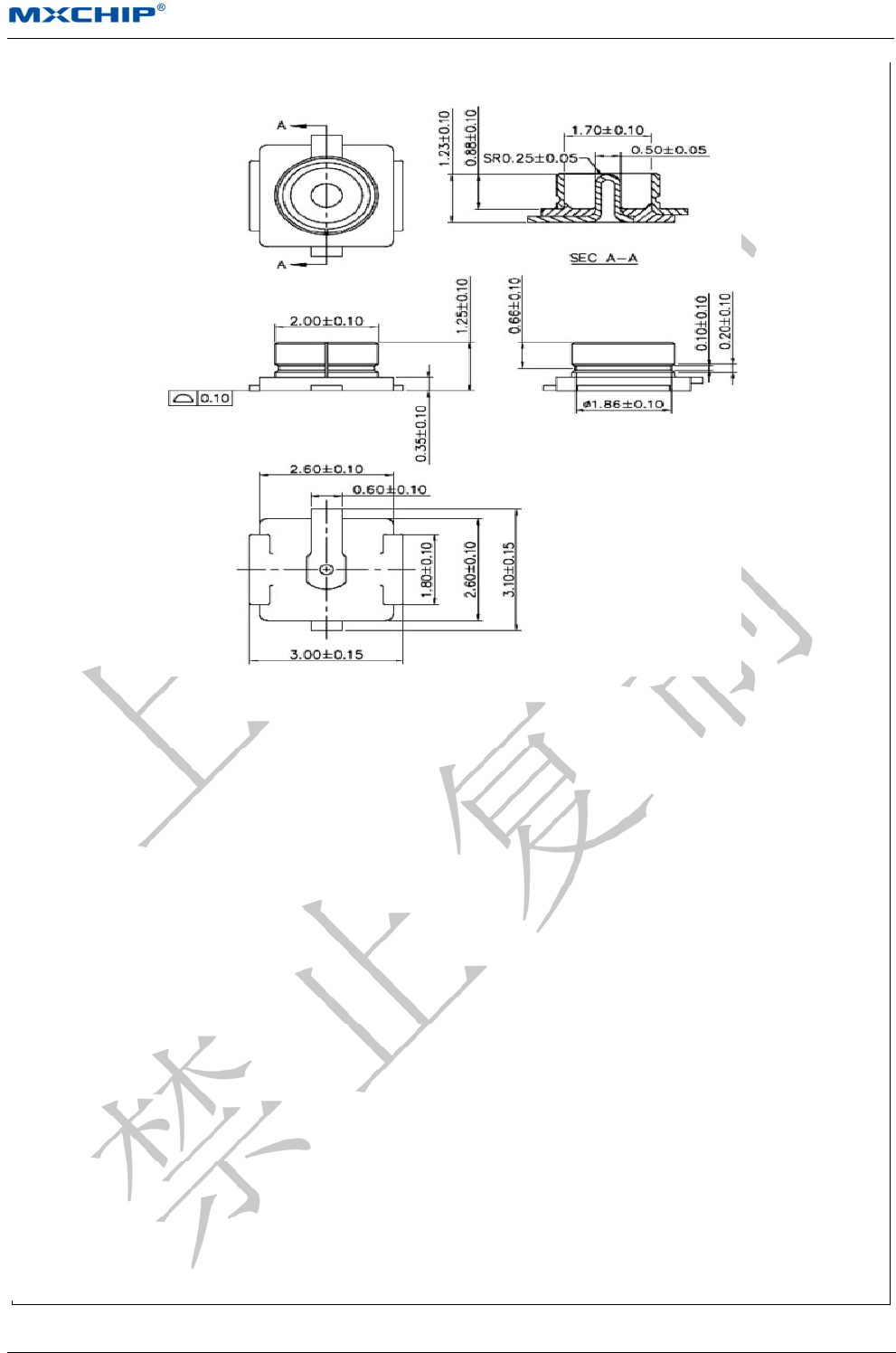
4.3 External Antenna Connector
Figure6Size of External Antenna Connector
MXCHIP All Rights Reserved
无法显示图像。计算机可能没有足够的内存以打开该图像,也可能是该图像已损坏。请重新启动计算机,然后重新打开该文件。如果仍然显示红色“x”,则可能需要删除该图像,然后重新将其插入。
Datasheet [Page 18]
EMW3080
5. Assembly Information and Production Guidance
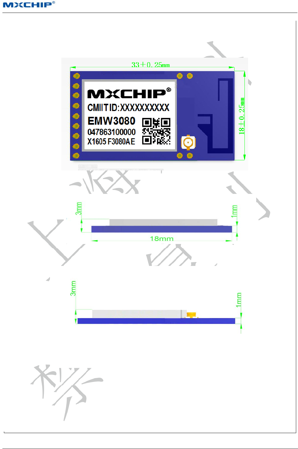
5.1 Assembly Size
Top View
Left Side View
Side View
Figure7EMW3080Side View (Unit: mm)
MXCHIP All Rights Reserved
无法显示图像。计算机可能没有足够的内存以打开该图像,也可能是该图像已损坏。请重新启动计算机,然后重新打开该文件。如果仍然显示红色“x”,则可能需要删除该图像,然后重新将其插入。
Datasheet [Page 19]
EMW3080
5.2 Production Guidance(Important)
The stamp hole package module produced by Mxchip must completely being patched by SMT machine
in 24 hours after open firmware package. Otherwise the module should be re-package by vacuum pumping
and drying before patch.
Devices for SMT patch:
(1)Reflow soldering machine
(2)AOI detector
(3)Suction nozzle with 6-8mm caliber
Device for drying:
(1)Cabinet type oven
(2)Anti-static and high thermotolerant tray
(3)Anti-static and high thermotolerant gloves
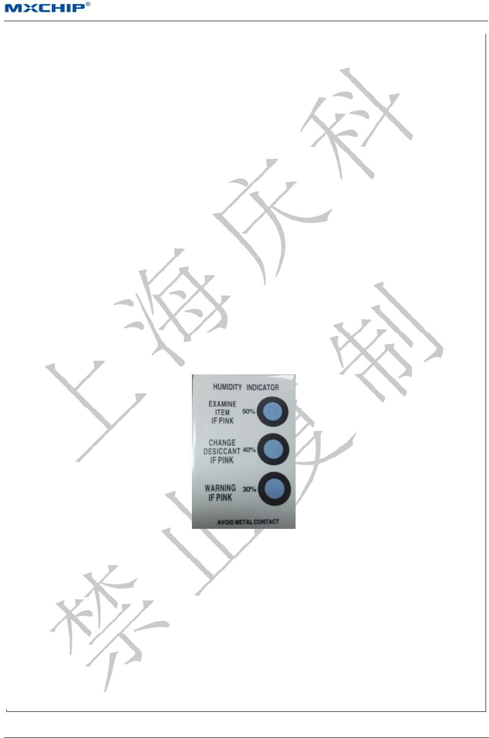
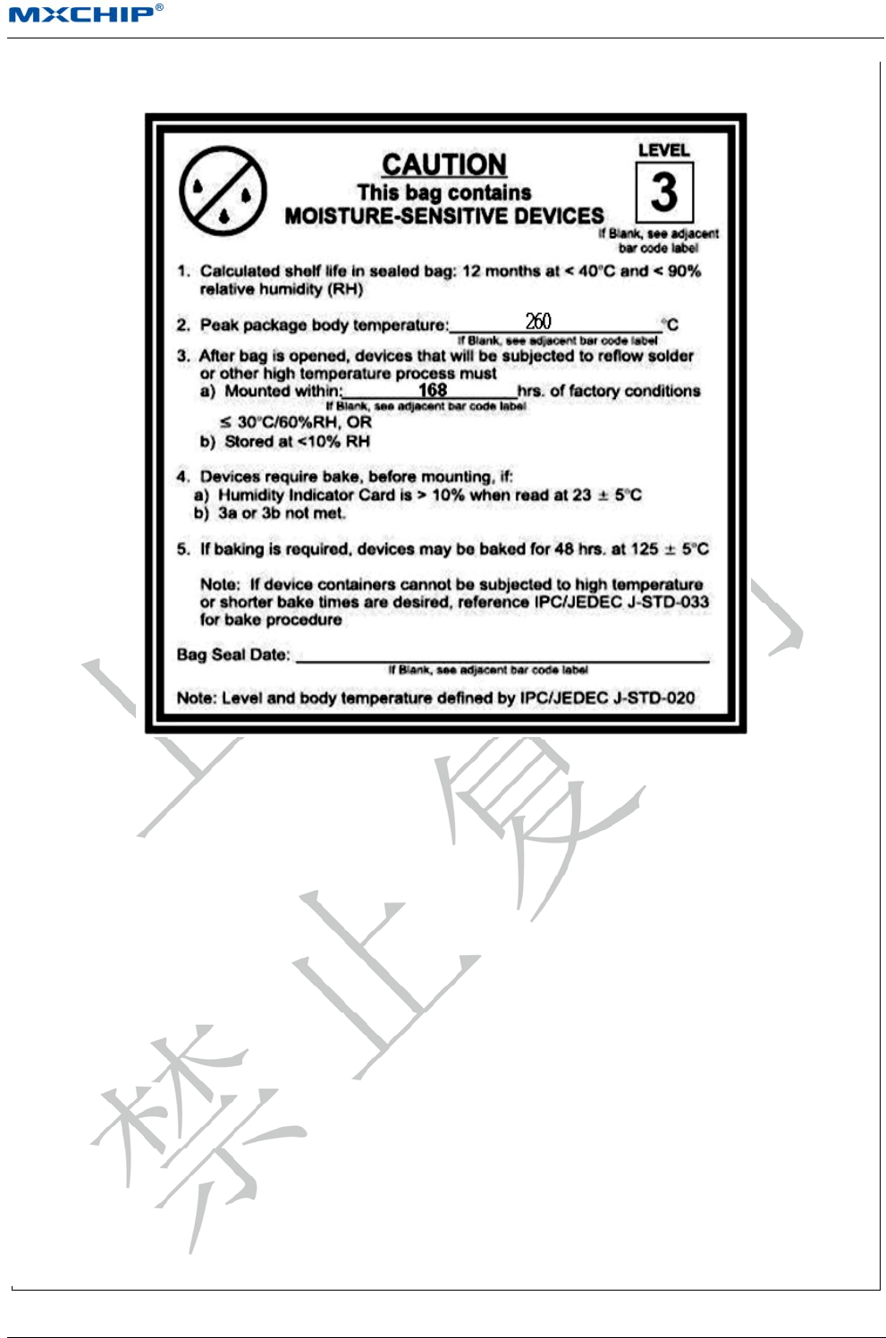
Conditions of product storage (Storage environment is shown in figure 8):
Moisture bag must be stored in temperature below 30 and humidity less than 85%RH.
Dry packaging products, the guarantee period should be from 6 months date of packing seal.
Humidity indicator card is in the hermetic package.
Figure8Humidity Card
Humidity indicator card and drying situation:
2 hours drying for module if the color ring at 30%, 40%, 50% in humidity indicator card is blue
after unpacking;
4 hours drying for module if the color ring at 30% in humidity indicator card is pink after
unpacking;
6 hours drying for module if the color ring at 30%, 40% in humidity indicator card is pink after
unpacking;
12 hours drying for module if the color ring at 30%, 40%, 50% in humidity indicator card is pink

MXCHIP All Rights Reserved
无法显示图像。计算机可能没有足够的内存以打开该图像,也可能是该图像已损坏。请重新启动计算机,然后重新打开该文件。如果仍然显示红色“x”,则可能需要删除该图像,然后重新将其插入。
Datasheet [Page 20]
EMW3080
after unpacking.
Drying parameters:
Drying temperature: 125℃±5℃;
Alarm temperature:130℃;
SMT patch when the device cool down below 36℃ in natural condition;
Dry times: 1;
Please dry again if the module is unsoldering in 12 hours after last drying.
SMT is unsuitable if the module packed over 3 months. There would be serious oxidation of the pad
because of immersion gold and cause false welding and lack of weld. Mxchip does not assume the
corresponding responsibility;
ESD protection is required before SMT;
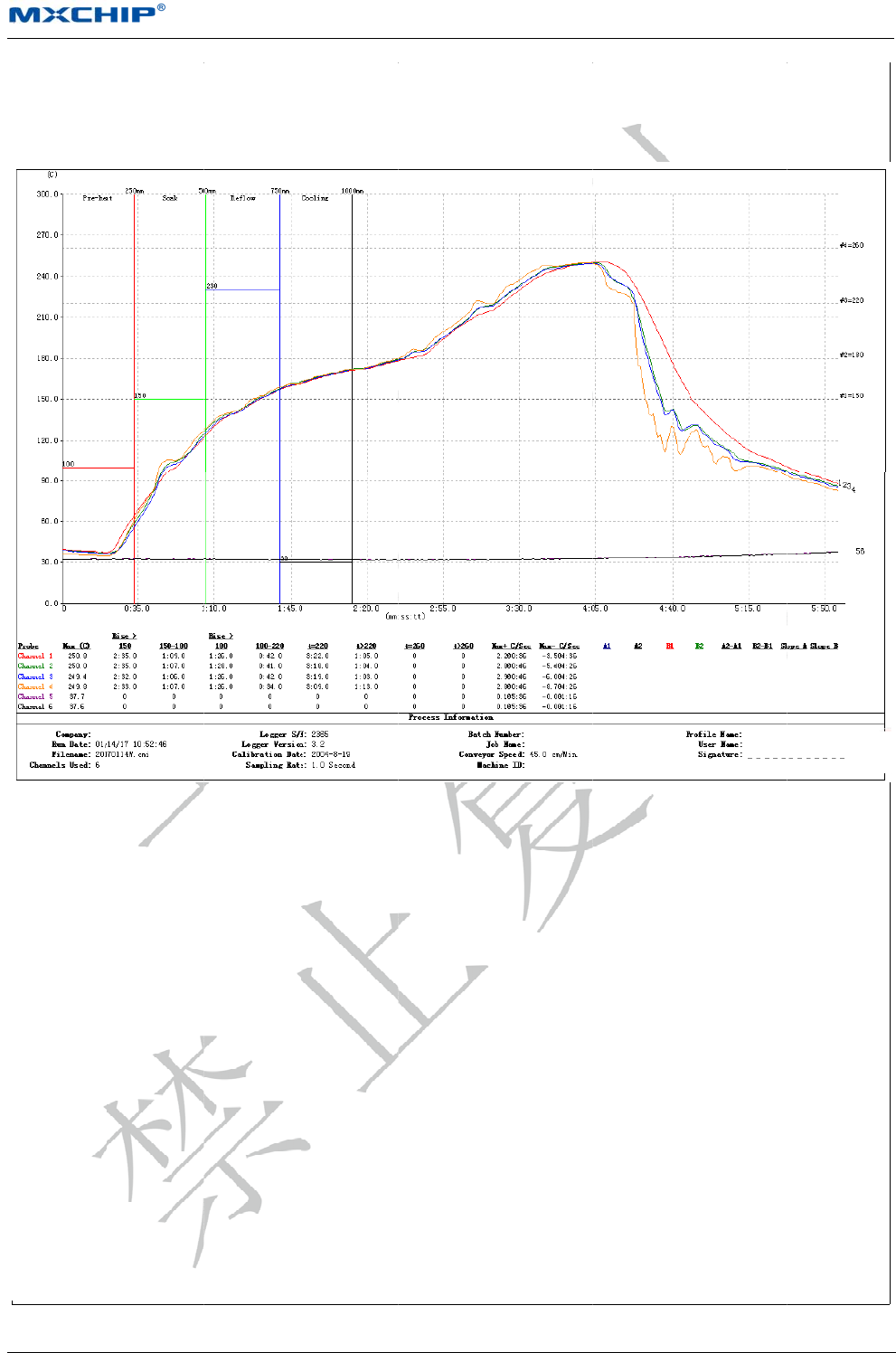
SMT patch should on the basis of reflow profile diagram, maximum temperature 245℃, reflow profile
diagram is shown in figure 10;
In order to guarantee the reflow soldering qualification rate, vision and AOI detection should be done in
10% products for the first patch to make sure the rationality of temperature control, device adsorption mode
and position. Detect 5 to 10 sample every hour in the following batch production.
5.3 Considerations
Operator should wear anti-static gloves during producing;
No more than drying time;
Any explosive, flammable and corrosivematerial is not allowed to add in drying;
Module should be put into oven with high thermotolerant tray. Ventilation should exist between each
module and no direct contact with oven;
Make sure oven is closed when drying to prevent temperature leaking;
Reduce opening time or keep closing the door of the oven during drying;
Use anti-static glove to take out module when its temperature below 36℃by natural cool down after
drying;
Make sure no water and dirt in the bottom of the module;
Temperature and humidity control is level 3 for initial modules. Storage and drying conditions are based
on IPC/JEDEC J-STD-020.
MXCHIP All Rights Reserved
无法显示图像。计算机可能没有足够的内存以打开该图像,也可能是该图像已损坏。请重新启动计算机,然后重新打开该文件。如果仍然显示红色“x”,则可能需要删除该图像,然后重新将其插入。
Datasheet [Page 21]
EMW3080
5.4 Storage Condition
Figure9Storage Condition
无法显示图像。计算机可能没有足够的内存以打开该图像,也可能是该图像已损坏。请重新启动计算机,然后重新打开该文件。如果仍然显示红色“x”,则可能需要删除该图
5.5 Te
m
Sugges
t
reflow.
像
,然后重新将其插入。
m
perature
t
ed solder pa
s
Curve o
f
s
te type: SA
C
Fig
u
D
f
Second
a
C
305, unlea
d
u
re10Tempe
r
MXCHIP All Rights Reserved
D
atasheet
EMW3080
a
r
y
Reflo
w
d
ed, solder p
a
r
ature Curve
w
a
ste thicknes
s
of Secondar
y
s
from 0.12
t
y
Reflow
t
o 0.15, less
[Page 22
than 2 times
]
MXCHIP All Rights Reserved
无法显示图像。计算机可能没有足够的内存以打开该图像,也可能是该图像已损坏。请重新启动计算机,然后重新打开该文件。如果仍然显示红色“x”,则可能需要删除该图像,然后重新将其插入。
Datasheet [Page 23]
EMW3080
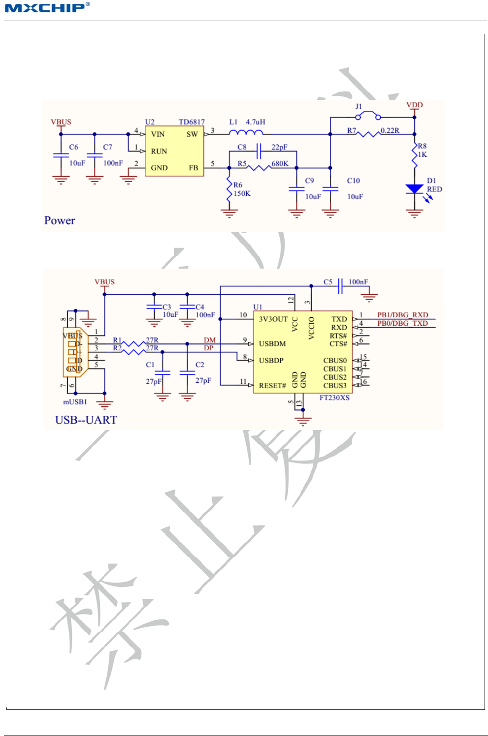
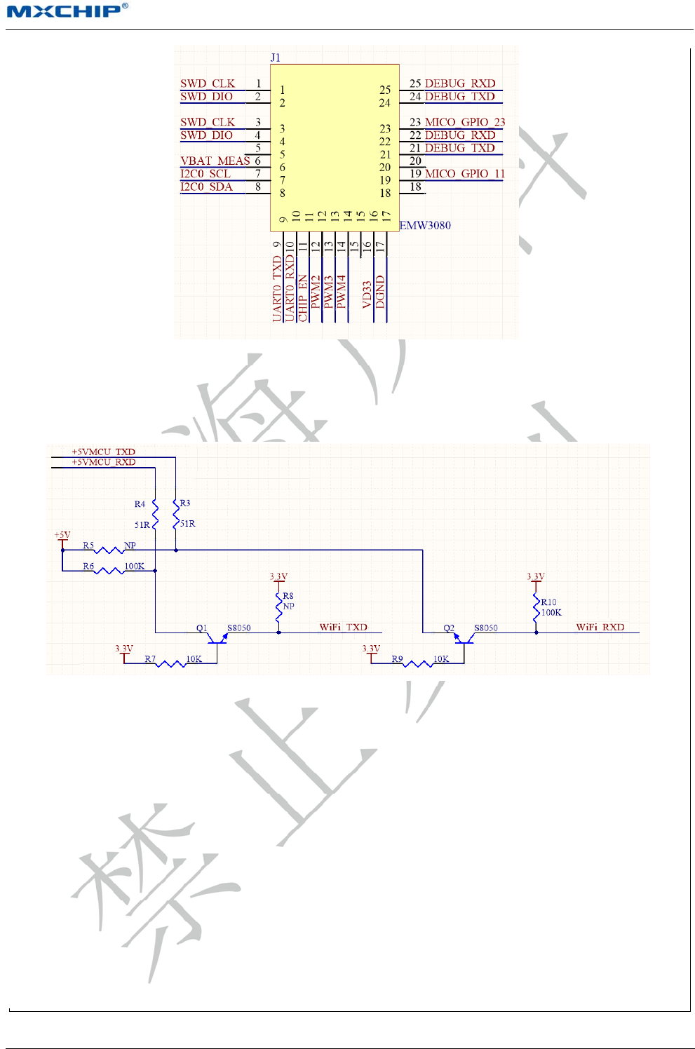
6. Reference Circuit
Power source circuit is shown in figure 11, USB to UART is shown in figure 12, external interface circuit is
shown in figure 13.
Figure11Power Source Circuit
Figure12USB to UART
MXCHIP All Rights Reserved
无法显示图像。计算机可能没有足够的内存以打开该图像,也可能是该图像已损坏。请重新启动计算机,然后重新打开该文件。如果仍然显示红色“x”,则可能需要删除该图像,然后重新将其插入。
Datasheet [Page 24]
EMW3080
Figure13External Interface Circuit of EMW3080
Voltage of EMW3239 UART is 3.3V. 5V UART should convert to 3.3V UART for the users that have 5V
chips. Convert circuit is shown in figure 14.
Figure143.3V UART- 5V UARTConvert Circuit

MXCHIP All Rights Reserved
无法显示图像。计算机可能没有足够的内存以打开该图像,也可能是该图像已损坏。请重新启动计算机,然后重新打开该文件。如果仍然显示红色“x”,则可能需要删除该图像,然后重新将其插入。
Datasheet [Page 25]
EMW3080
7. ModuleMOQ and Package Information
Table 16 ModuleMOQ and Package Information
Type MOQ(pcs)
Shipping
packing method
(Tray/Tape)
Module storage
quantity for
each tray (pcs)
Tray number
for each box
Module quantity
for each box (pcs)
EMW3080(AP)
EMW3080(AE)
EMW3080(BP)
EMW3080(BE)
1050(2 boxes) Tray 35 15+1 525

MXCHIP All Rights Reserved
无法显示图像。计算机可能没有足够的内存以打开该图像,也可能是该图像已损坏。请重新启动计算机,然后重新打开该文件。如果仍然显示红色“x”,则可能需要删除该图像,然后重新将其插入。
Datasheet [Page 26]
EMW3080
8. FCC Caution
§ 15.19 Labeling requirements.
This device complies with part 15 of the FCC Rules. Operation is subject to the following two conditions: (1)
This device may not cause harmful interference, and (2) this device must accept any interference received,
including interference that may cause undesired operation.
§ 15.21 Information to user.
Any Changes or modifications not expressly approved by the party responsible for compliance could void the
user's authority to operate the equipment.
§ 15.105 Information to the user.
Note: This equipment has been tested and found to comply with the limits for a Class B digital device,
pursuant to part 15 of the FCC Rules. These limits are designed to provide reasonable protection against harmful
interference in a residential installation. This equipment generates uses and can radiate radio frequency energy and,
if not installed and used in accordance with the instructions, may cause harmful interference to radio
communications. However, there is no guarantee that interference will not occur in a particular installation. If this
equipment does cause harmful interference to radio or television reception, which can be determined by turning
the equipment off and on, the user is encouraged to try to correct the interference by one or more of the following
measures:
-Reorient or relocate the receiving antenna.
-Increase the separation between the equipment and receiver.
-Connect the equipment into an outlet on a circuit different from that to which the receiver is connected.
-Consult the dealer or an experienced radio/TV technician for help.
This equipment complies with FCC radiation exposure limits set forth for an
uncontrolled environment. This equipment should be installed and operated withminimum distance 20cm between
the radiator & your body.
This module is intended for OEM integrator. The OEM integrator is still responsible for the FCC compliance
requirement of the end product which integrates this module.
The final end product must be labeled in a visible area with the following
" Contains TX FCC ID: P53-EMW3080".
MXCHIP All Rights Reserved
无法显示图像。计算机可能没有足够的内存以打开该图像,也可能是该图像已损坏。请重新启动计算机,然后重新打开该文件。如果仍然显示红色“x”,则可能需要删除该图像,然后重新将其插入。
Datasheet [Page 27]
EMW3080
9. CE Caution
Complies with the essential protection requirements of Directives on Radio Equipment Directive
2014/53/EU.
This declaration applies to all specimens manufactured identical to the samples submitted for
testing/evaluation.
The assessments were based on the following regulations and standards:
Requirement Standard Report No. Assessment Body
Health and
safety
EN 60950-1:2006+A11:2009+A1:2010+A12:2011+A2:2013
EN 62311:2008;
SET2017-04238
SET2017-04738 Telefication B.V
EMC
Draft EN 301 489-1 V2.2.0
Draft EN 301 489-17 V3.2.0
SET2017-03082 Telefication B.V
Radio
Spectrum
EN 300 328 V2.1.1
SET2017-03256 Telefication B.V
This declaration is the responsibility of the manufacturer:

MXCHIP All Rights Reserved
无法显示图像。计算机可能没有足够的内存以打开该图像,也可能是该图像已损坏。请重新启动计算机,然后重新打开该文件。如果仍然显示红色“x”,则可能需要删除该图像,然后重新将其插入。
Datasheet [Page 28]
EMW3080
10. Sales Information and Technical Support
Company: Shanghai MXCHIP Information Technology Co., Ltd
For consultation or purchase the product, please contact Mxchip during working hours:
From Monday to Friday, morning 9:00~12:00, afternoon 13:00~18:00
Telephone: +86-21-52655026
Contact address: 9thFloor, No.5, Lane2145 JinshaJiang Road Putuo District, ShangHai.
Postcode:200333
Email: sales@mxchip.com