MXCHIP Information Technology EMW3090 Embedded WIFI module User Manual
Shanghai MXCHIP Information Technology Co.,Ltd. Embedded WIFI module Users Manual
UserManual.wiki
>
MXCHIP Information Technology
>
EMW3090 User Manual
User Manual
Navigation menu
Upload a User Manual
Namespaces
Wiki Guide
HTML
PDF
Info
Views
User Manual
Discussion / Help
Navigation
![Datasheet [Page 1]EMW3090Version IllustrationDateVisionDetails2017-06-121.0Initial document](https://usermanual.wiki/MXCHIP-Information-Technology/EMW3090/User-Guide-3628110-Page-2.png)
![Datasheet [Page 2]EMW3090ContentAbstract..................................................................................................................................................................................1Version Illustration............................................................................................................................................................... 11.1 EMW3090 LABEL INFORMATION............................................................................................................................. 51.2 PIN ARRANGEMENT................................................................................................................................................... 51.3 PIN DEFINITION......................................................................................................................................................... 61.3.1 EMW3090 Package Definition..................................................................................................................61.3.2 EMW3090 Pin Definition..........................................................................................................................72. Electrical Parameters....................................................................................................................................................... 82.1 OPERATING CONDITIONS...........................................................................................................................................82.2 POWER CONSUMPTION...............................................................................................................................................82.3 WORKING ENVIRONMENT..........................................................................................................................................92.4 ELECTROSTATIC DISCHARGE..................................................................................................................................... 93. RF parameters.................................................................................................................................................................103.1 BASIC RF PARAMETERS...........................................................................................................................................104. Antenna Information...................................................................................................................................................... 114.1 ANTENNA TYPE........................................................................................................................................................ 114.2 PCB ANTENNA CLEARANCE ZONE&PCB ANT PARAMETER.................................................................................. 114.3 EXTERNAL ANTENNA CONNECTOR&EXTERNAL ANTENNA PARAMETERS................................................................ 125. Production Guidance(Important)............................................................................................................................ 145.1 CONSIDERATIONS.................................................................................................................................................... 155.2 STORAGE CONDITION.............................................................................................................................................. 165.3 TEMPERATURE CURVE OF SECONDARY REFLOW.....................................................................................................176. Reference Circuit............................................................................................................................................................ 187. Sales Information and Technical Support.................................................................................................................... 20](https://usermanual.wiki/MXCHIP-Information-Technology/EMW3090/User-Guide-3628110-Page-3.png)
![Datasheet [Page 3]EMW3090Figure ContentFigure 1 EMW3090 Label Information...............................................................................................................5Figure 2 Half-hole SMT Package Size.............................................................................................................. 6Figure 3 EMW3090 Package Definition............................................................................................................. 6Figure 4 Minimum Clearance Zone of PCB Antenna (Unit: mm)................................................................... 12Figure 5 Size of External Antenna Connector...................................................................................................13Figure 6 Humidity Card.....................................................................................................................................14Figure 7 Storage Condition................................................................................................................................16Figure 8 Temperature Curve of Secondary Reflow...........................................................................................17Figure 9 Power Source Circuit.......................................................................................................................... 18Figure 10 USB to UART................................................................................................................................... 18Figure 11 External Interface Circuit of EMW3090...........................................................................................18Figure 12 3.3V UART- 5V UART Convert Circuit...........................................................................................19](https://usermanual.wiki/MXCHIP-Information-Technology/EMW3090/User-Guide-3628110-Page-4.png)
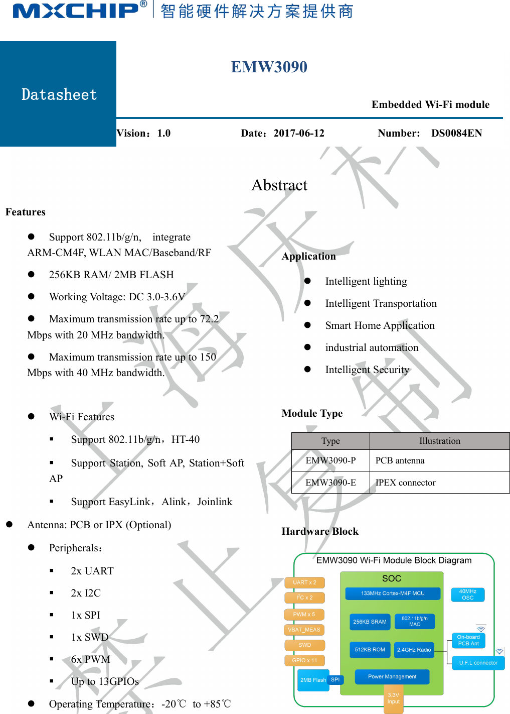
![Datasheet [Page 4]EMW3090Product IntroductionEMW3090 is a cost-effective embedded Wi-Fi module released by MXCHIP with high integrating ARMCM4F, WLAN MAC/Baseband/RF. Maximum frequency 133MHz with 256KB SRAM and 2M FLASH. Powersupply is DC 3.3V. Mounting mode is SMT or DIP(Dual In-line Package). Peripherals: 2xUART / 1x SPI /2x I2C /6x PWM / Up to 13 GPIOs.EMW3090 runs MiCO 3.0 IoT operating system, supporting Micoder IDE. Provide fast, stable and secureend-to-end cloud links to users with integrate TCP/IP protocol stack, various security encryption algorithm,intelligent cloud such as MXCHIP easylink/Alink 1.1/Joinlink 3.0/Hilink/One Net/Gome/Suning, oversea cloudsuch as AWS/Ayla/Azure/IBM Watson/Google/Apple Homekit.Hardware diagram is shown below with four main parts:CM4F main coreWLAN MAC/BB/RF/ANTHardware encryptionPower managementWith:1. ARM CM4F CPU with 133MHz maximum frequency and 256KB SRAM and 2M FLASH. Support highspeed UART, I2C, SPI, PWM and multi-GPIO.2. 2MB SPI Flash is used for custom firmware development3. Support PCB antenna and IPEX4. Input voltage: DC 3.3VEMW3090 Hardware block](https://usermanual.wiki/MXCHIP-Information-Technology/EMW3090/User-Guide-3628110-Page-5.png)
![Datasheet [Page 5]EMW30901.1 EMW3090 Label InformationFigure 1 EMW3090 Label InformationLabel Information:CMIIT ID:XXXXXXXX : SRRC approval numberEMW3090: Module type047863100000:MAC address (Each module has a unique MAC address)X1701:production batchXXXX.XXXX.XXXX : SN series number1.2 Pin ArrangementEMW3090 has half-hole SMT package.Solder mask openness has the same size with land. The width of steel mesh is suggested to be 0.12mm to0.14mm in SMT.](https://usermanual.wiki/MXCHIP-Information-Technology/EMW3090/User-Guide-3628110-Page-6.png)
![Datasheet [Page 6]EMW3090Figure 2 Half-hole SMT Package Size1.3 Pin Definition1.3.1 EMW3090 Package DefinitionFigure 3 EMW3090 Package Definition](https://usermanual.wiki/MXCHIP-Information-Technology/EMW3090/User-Guide-3628110-Page-7.png)
![Datasheet [Page 7]EMW30901.3.2 EMW3090 Pin DefinitionTable 1 EMW3090 Pin DefinitionPinNO.FUNCTION1FUNCTION2FUNCTION3FUNCTION4FUNCTION51VDD2CHIP_EN3MICO_GPIO_12MICO_PWM34MICO_GPIO_13MICO_PWM45MICO_GPIO_8MICO_I2C0_SDAMICO_UART0_CTSMICO_SPI1_CS6MICO_GPIO_7MICO_I2C0_SCLMICO_UART0_RTSMICO_PWM6MICO_SPI1_MISO7MICO_GPIO_21MICO_I2C0_SDAMICO_UART1_TXDMICO_PWM48MICO_GPIO_22MICO_I2C0_SCLMICO_UART1_RXDMICO_PWM59GND10MICO_GPIO_14MICO_PWM511MICO_GPIO_10MICO_I2C1_CLKMICO_UART0_RXDMICO_SPI1_CLK12MICO_GPIO_9MICO_I2C1_SDAMICO_UART0_TXDMICO_PWM1MICO_SPI1_MOSI13GND14MICO_GPIO_2315VBAT_MEAS16NC17MICO_GPIO_1918GNDNotes:(1) PIN 17 is used as BOOT,PIN14 is used as EASYLINK, please do not use pin 7 and 8 in hardwaredesign. Please contact engineer of MXCHIP if it is necessary to use the two pins.(2) PIN7/8 should be in high voltage or NC when power on, please aware it when designing circuit.(3) If not used, please set the pin as NC, especially for CHIP_EN.](https://usermanual.wiki/MXCHIP-Information-Technology/EMW3090/User-Guide-3628110-Page-8.png)
![Datasheet [Page 8]EMW30902. Electrical Parameters2.1 Operating ConditionsEMW3090 would be unstable when input voltage is less than the lowest rated voltage.Table 2 Range of input voltageSymbolIllustrationConditionDetailsMinimumTypMaximumUnitVDDPower Supply3.03.33.6VThere would be permanent damage in hardware if the device operates at the voltage over rated value.Meanwhile, reliability could be influenced when the device has a long-term operating at maximum voltage.Table 3 Absolute maximum voltage ratingSymbolDescriptionMinimumTypUnitVDDModule input voltage–0.33.6VVINGPIO input voltage−0.33.6V2.2 Power ConsumptionTable 4 EMW3090 Power ConsumptionStatusAverage current(3V3)Max current(3V3)DescriptionWIFI Initialization26.91mA33.1mAWIFI low power mode enabledWIFI Connected47.71mA119.5mAKeep connected with the routerWIFI low power mode enabledUDP transmission168.37mA298.7mAWIFI low power mode disabledSoftAP121.48mA260.4mASoftAP connect to internetEasylink122.84mA136.7mAProcess of module network distributionStandby10.45uA12.07uAUltra low standby power modeActual working current is variable at different operating mode. Maximum operating current 300 mA 。](https://usermanual.wiki/MXCHIP-Information-Technology/EMW3090/User-Guide-3628110-Page-9.png)
![Datasheet [Page 9]EMW30902.3 Working EnvironmentTable 5 Temperature and humidity conditionSymbolNameMaximumUnitTSTGStorage Temperature-20 to +85℃TAOperation Temperature-20 to +85℃HumidityNon-condensing, Relative humidity95%2.4 Electrostatic DischargeTable 6 Electrostatic Discharge ParametersSymbolNameDetailsLevelMaximumUnitVESD(HBM)Electrostatic dischargevoltage(Human Body Model)TA= +25 °C , JESD22-A11422000VVESD(CDM)Electrostatic dischargevoltage(Charged DeviceModel)TA = +25 °C , JESD22-C101II500](https://usermanual.wiki/MXCHIP-Information-Technology/EMW3090/User-Guide-3628110-Page-10.png)
![Datasheet [Page 10]EMW30903. RF parameters3.1 Basic RF parametersTable 7 Radio-frequency standardsNameIllustrationWorking frequency2.412~2.472GHzWi-Fi wireless standardIEEE802.11b/g/nDatatransmission rate20MHz11b:1,2,5.5 和11Mbps11g : 6,9,12,18,24,36,48,54Mbps11n : MCS0~7,72.2Mbps40MHz11n:MCS0~7,150MbpsAntenna typePCB (Default)IPX (Optional)](https://usermanual.wiki/MXCHIP-Information-Technology/EMW3090/User-Guide-3628110-Page-11.png)
![Datasheet [Page 11]EMW30904. Antenna Information4.1 Antenna TypeEMW3090 has two type of antenna: EMW3090-P and EMW3090-EEWM3090-P EMW3090-E4.2 PCB Antenna Clearance Zone&PCB ANT parameterMain PCB should have a distance over 16mm with other metal elements when using PCB antenna in Wi-Fidevice. Shadow parts in the figure below should keep away from metal elements, sensor, interference source andother material that could cause signal interference.](https://usermanual.wiki/MXCHIP-Information-Technology/EMW3090/User-Guide-3628110-Page-12.png)
![Datasheet [Page 12]EMW3090Figure 4 Minimum Clearance Zone of PCB Antenna (Unit: mm)4.3 External Antenna Connector&External antenna parameters1、External Antenna Parameter:Model name:IPEX1.3-2.4G-L1312、External Antenna Connector](https://usermanual.wiki/MXCHIP-Information-Technology/EMW3090/User-Guide-3628110-Page-13.png)
![Datasheet [Page 13]EMW3090Figure 5 Size of External Antenna Connector3、antenna trace design The characteristic impedance depends on the dielectric of PCB, the track width and the Ground plane spacing. Microstrip type is required. The detail simulation as below.The RE trace of the test board which was used in the FCC test is defined as below.](https://usermanual.wiki/MXCHIP-Information-Technology/EMW3090/User-Guide-3628110-Page-14.png)
![Datasheet [Page 14]EMW30905. Production Guidance(Important)The stamp hole package module produced by Mxchip must completely being patched by SMT machinein 24 hours after open firmware package. Otherwise the module should be re-package by vacuum pumpingand drying before patch.Devices for SMT patch:(1)Reflow soldering machine(2)AOI detector(3)Suction nozzle with 6-8mm caliberDevice for drying:(1)Cabinet type oven(2)Anti-static and high thermos tolerant tray(3)Anti-static and high thermos tolerant glovesConditions of product storage (Storage environment is shown in figure 8):Moisture bag must be stored in temperature below 30 and humidity less than 85%RH.Dry packaging products, the guarantee period should be from 6 months date of packing seal.Humidity indicator card is in the hermetic package.Figure 6 Humidity CardHumidity indicator card and drying situation:2 hours drying for module if the color ring at 30%, 40%, 50% in humidity indicator card is blueafter unpacking;4 hours drying for module if the color ring at 30% in humidity indicator card is pink afterunpacking;6 hours drying for module if the color ring at 30%, 40% in humidity indicator card is pink after](https://usermanual.wiki/MXCHIP-Information-Technology/EMW3090/User-Guide-3628110-Page-15.png)
![Datasheet [Page 15]EMW3090unpacking;12 hours drying for module if the color ring at 30%, 40%, 50% in humidity indicator card is pinkafter unpacking.Drying parameters:Drying temperature: 125℃±5℃;Alarm temperature: 130℃;SMT patch when the device cool down below 36℃in natural condition;Dry times: 1;Please dry again if the module is unsoldering in 12 hours after last drying.SMT is unsuitable if the module packed over 3 months. There would be serious oxidation of the padbecause of immersion gold and cause false welding and lack of weld. Mxchip does not assume thecorresponding responsibility;ESD protection is required before SMT;SMT patch should on the basis of reflow profile diagram, maximum temperature 245℃, reflow profilediagram is shown in figure 10;In order to guarantee the reflow soldering qualification rate, vision and AOI detection should be done in10% products for the first patch to make sure the rationality of temperature control, device adsorption modeand position. Detect 5 to 10 sample every hour in the following batch production.5.1 ConsiderationsOperator should wear anti-static gloves during producing;No more than drying time;Any explosive, flammable and corrosive material is not allowed to add in drying;Module should be put into oven with high thermotolerant tray. Ventilation should exist between eachmodule and no direct contact with oven;Make sure oven is closed when drying to prevent temperature leaking;Reduce opening time or keep closing the door of the oven during drying;Use anti-static glove to take out module when its temperature below 36℃by natural cool down afterdrying;Make sure no water and dirt in the bottom of the module;Temperature and humidity control is level 3 for initial modules. Storage and drying conditions are basedon IPC/JEDEC J-STD-020.](https://usermanual.wiki/MXCHIP-Information-Technology/EMW3090/User-Guide-3628110-Page-16.png)
![Datasheet [Page 16]EMW30905.2 Storage ConditionFigure 7 Storage Condition](https://usermanual.wiki/MXCHIP-Information-Technology/EMW3090/User-Guide-3628110-Page-17.png)
![Datasheet [Page 17]EMW30905.3 Temperature Curve of Secondary ReflowSuggested solder paste type: SAC305, unleaded, solder paste thickness from 0.12 to 0.15, less than 2 timesreflow.Figure 8 Temperature Curve of Secondary Reflow](https://usermanual.wiki/MXCHIP-Information-Technology/EMW3090/User-Guide-3628110-Page-18.png)
![Datasheet [Page 18]EMW30906. Reference CircuitPower source circuit is shown in figure 9, USB to UART is shown in figure 10, external interface circuit isshown in figure 11.Figure 9 Power Source CircuitFigure 10 USB to UARTFigure 11 External Interface Circuit of EMW3090](https://usermanual.wiki/MXCHIP-Information-Technology/EMW3090/User-Guide-3628110-Page-19.png)
![Datasheet [Page 19]EMW3090Voltage of EMW3090 UART is 3.3V. 5V UART should convert to 3.3V UART for the users that have 5Vchips. Convert circuit is shown in figure 14.Figure 12 3.3V UART- 5V UART Convert Circuit](https://usermanual.wiki/MXCHIP-Information-Technology/EMW3090/User-Guide-3628110-Page-20.png)
![Datasheet [Page 20]EMW30907. Sales Information and Technical SupportFor consultation or purchase the product, please contact Mxchip during working hours:From Monday to Friday, morning 9:00~12:00, afternoon 13:00~18:00Telephone: +86-21-52655026Contact address: 9thFloor, No.5, Lane2145 JinshaJiang Road Putuo District, ShangHai.Postcode:200333Email: sales@mxchip.com](https://usermanual.wiki/MXCHIP-Information-Technology/EMW3090/User-Guide-3628110-Page-21.png)
![Datasheet [Page 1]EMW3090FCC Regulations:This device complies with part 15 of the FCC Rules. Operation is subject to the following twoconditions: (1) This device may not cause harmful interference, and (2) This device must accept anyinterference received, including interference that may cause undesired operation.This device has been tested and found to comply with the limits for a Class B digital device ,pursuant to Part 15 of the FCC Rules. These limits are designed to provide reasonable protectionagainst harmful interference in a residential installation. This equipment generates, uses and canradiated radio frequency energy and, if not installed and used in accordance with the instructions,may cause harmful interference to radio communications. However, there is no guarantee thatinterference will not occur in a particular installation If this equipment does cause harmfulinterference to radio or television reception, which can be determined by turning the equipment offand on, the user is encouraged to try to correct the interference by one or more of the followingmeasures:-Reorient or relocate the receiving antenna.-Increase the separation between the equipment and receiver.-Connect the equipment into an outlet on a circuit different from that to which the receiver isconnected.-Consult the dealer or an experienced radio/TV technician for help.Caution: Changes or modifications not expressly approved by the party responsible forcompliance could void the user‘s authority to operate the equipment.RF Exposure InformationThis device complies with FCC radiation exposure limits set forth for an uncontrolledenvironment. In order to avoid the possibility of exceeding the FCC radio frequency exposure limits,human proximity to the antenna shall not be less than 20cm (8 inches) during normal operation.IMPORTANT NOTE:This module is intended for OEM integrator. The OEM integrator is still responsible for the FCCcompliance requirement of the end product, which integrates this module. 20cm minimum distancehas to be able to be maintained between the antenna and the users for the host this module isintegrated into. Under such configuration, the FCC radiation exposure limits set forth for anpopulation/uncontrolled environment can be satisfied.Any changes or modifications not expressly approved by the manufacturer could void the user'sauthority to operate this equipment.](https://usermanual.wiki/MXCHIP-Information-Technology/EMW3090/User-Guide-3628110-Page-22.png)
![Datasheet [Page 2]EMW3090USERS MANUAL OF THE END PRODUCT:In the users manual of the end product, the end user has to be informed to keep at least 20cmseparation with the antenna while this end product is installed and operated. The end user has to beinformed that the FCC radio-frequency exposure guidelines for an uncontrolled environment can besatisfied. The end user has to also be informed that any changes or modifications not expresslyapproved by the manufacturer could void the user's authority to operate this equipment. If the size ofthe end product is smaller than 8x10cm, then additional FCC part 15.19 statement is required to beavailable in the users manual: This device complies with Part 15 of FCC rules. Operation is subject tothe following two conditions: (1) this device may not cause harmful interference and (2) this devicemust accept any interference received, including interference that may cause undesired operation.LABEL OF THE END PRODUCT:The final end product must be labeled in a visible area with the following " Contains TransmitterModule FCC ID: P53-EMW3090 ". If the size of the end product is larger than 8x10cm, then thefollowing FCC part 15.19 statement has to also be available on the label: This device complies withPart 15 of FCC rules.Operation is subject to the following two conditions: (1) this device may not cause harmfulinterference and (2) this device must accept any interference received, including interference thatmay cause undesired operation.](https://usermanual.wiki/MXCHIP-Information-Technology/EMW3090/User-Guide-3628110-Page-23.png)