MXCHIP Information Technology EMW3090 Embedded WIFI module User Manual
Shanghai MXCHIP Information Technology Co.,Ltd. Embedded WIFI module Users Manual
User Manual
Abstract
Features
Support 802.11b/g/n, integrate
ARM-CM4F, WLAN MAC/Baseband/RF
256KB RAM/ 2MB FLASH
Working Voltage: DC 3.0-3.6V
Maximum transmission rate up to 72.2
Mbps with 20 MHz bandwidth.
Maximum transmission rate up to 150
Mbps with 40 MHz bandwidth.
Wi-Fi Features
Support 802.11b/g/n,HT-40
Support Station, Soft AP, Station+Soft
AP
Support EasyLink,Alink,Joinlink
Antenna: PCB or IPX (Optional)
Peripherals:
2x UART
2x I2C
1x SPI
1x SWD
6x PWM
Up to 13GPIOs
Operating Temperature:-20℃to +85℃
Application
Intelligent lighting
Intelligent Transportation
Smart Home Application
industrial automation
Intelligent Security
Module Type
Type
Illustration
EMW3090-P
PCB antenna
EMW3090-E
IPEX connector
Hardware Block
Datasheet
EMW3090
Embedded Wi-Fi module
Vision:1.0
Date:2017-06-12
Number: DS0084EN

Datasheet [Page 1]
EMW3090
Version Illustration
Date
Vision
Details
2017-06-12
1.0
Initial document

Datasheet [Page 2]
EMW3090
Content
Abstract..................................................................................................................................................................................1
Version Illustration............................................................................................................................................................... 1
1.1 EMW3090 LABEL INFORMATION............................................................................................................................. 5
1.2 PIN ARRANGEMENT................................................................................................................................................... 5
1.3 PIN DEFINITION......................................................................................................................................................... 6
1.3.1 EMW3090 Package Definition..................................................................................................................6
1.3.2 EMW3090 Pin Definition..........................................................................................................................7
2. Electrical Parameters....................................................................................................................................................... 8
2.1 OPERATING CONDITIONS...........................................................................................................................................8
2.2 POWER CONSUMPTION...............................................................................................................................................8
2.3 WORKING ENVIRONMENT..........................................................................................................................................9
2.4 ELECTROSTATIC DISCHARGE..................................................................................................................................... 9
3. RF parameters.................................................................................................................................................................10
3.1 BASIC RF PARAMETERS...........................................................................................................................................10
4. Antenna Information...................................................................................................................................................... 11
4.1 ANTENNA TYPE........................................................................................................................................................ 11
4.2 PCB ANTENNA CLEARANCE ZONE&PCB ANT PARAMETER.................................................................................. 11
4.3 EXTERNAL ANTENNA CONNECTOR&EXTERNAL ANTENNA PARAMETERS................................................................ 12
5. Production Guidance(Important)............................................................................................................................ 14
5.1 CONSIDERATIONS.................................................................................................................................................... 15
5.2 STORAGE CONDITION.............................................................................................................................................. 16
5.3 TEMPERATURE CURVE OF SECONDARY REFLOW.....................................................................................................17
6. Reference Circuit............................................................................................................................................................ 18
7. Sales Information and Technical Support.................................................................................................................... 20

Datasheet [Page 3]
EMW3090
Figure Content
Figure 1 EMW3090 Label Information...............................................................................................................5
Figure 2 Half-hole SMT Package Size.............................................................................................................. 6
Figure 3 EMW3090 Package Definition............................................................................................................. 6
Figure 4 Minimum Clearance Zone of PCB Antenna (Unit: mm)................................................................... 12
Figure 5 Size of External Antenna Connector...................................................................................................13
Figure 6 Humidity Card.....................................................................................................................................14
Figure 7 Storage Condition................................................................................................................................16
Figure 8 Temperature Curve of Secondary Reflow...........................................................................................17
Figure 9 Power Source Circuit.......................................................................................................................... 18
Figure 10 USB to UART................................................................................................................................... 18
Figure 11 External Interface Circuit of EMW3090...........................................................................................18
Figure 12 3.3V UART- 5V UART Convert Circuit...........................................................................................19
Datasheet [Page 4]
EMW3090
Product Introduction
EMW3090 is a cost-effective embedded Wi-Fi module released by MXCHIP with high integrating ARM
CM4F, WLAN MAC/Baseband/RF. Maximum frequency 133MHz with 256KB SRAM and 2M FLASH. Power
supply is DC 3.3V. Mounting mode is SMT or DIP(Dual In-line Package). Peripherals: 2xUART / 1x SPI /2x I2C /
6x PWM / Up to 13 GPIOs.
EMW3090 runs MiCO 3.0 IoT operating system, supporting Micoder IDE. Provide fast, stable and secure
end-to-end cloud links to users with integrate TCP/IP protocol stack, various security encryption algorithm,
intelligent cloud such as MXCHIP easylink/Alink 1.1/Joinlink 3.0/Hilink/One Net/Gome/Suning, oversea cloud
such as AWS/Ayla/Azure/IBM Watson/Google/Apple Homekit.
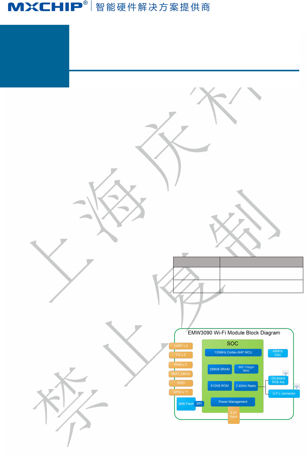
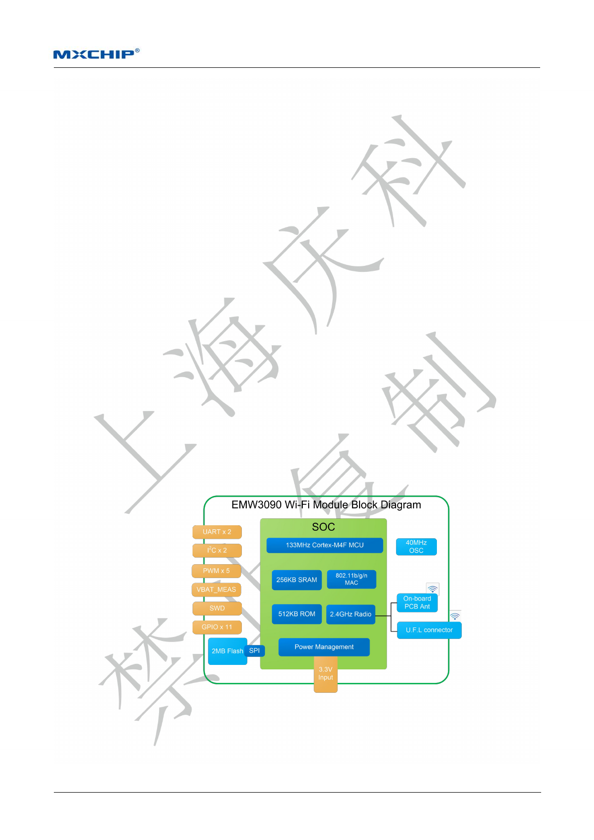
Hardware diagram is shown below with four main parts:
CM4F main core
WLAN MAC/BB/RF/ANT
Hardware encryption
Power management
With:
1. ARM CM4F CPU with 133MHz maximum frequency and 256KB SRAM and 2M FLASH. Support high
speed UART, I2C, SPI, PWM and multi-GPIO.
2. 2MB SPI Flash is used for custom firmware development
3. Support PCB antenna and IPEX
4. Input voltage: DC 3.3V
EMW3090 Hardware block
Datasheet [Page 5]
EMW3090
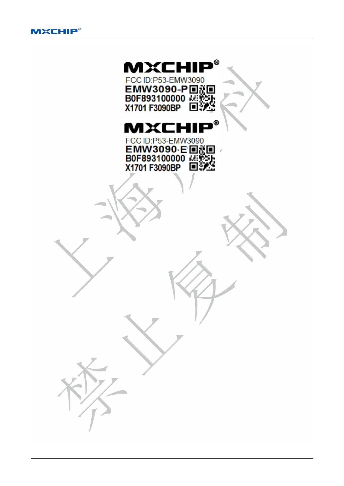
1.1 EMW3090 Label Information
Figure 1 EMW3090 Label Information
Label Information:
CMIIT ID:XXXXXXXX : SRRC approval number
EMW3090: Module type
047863100000:MAC address (Each module has a unique MAC address)
X1701:production batch
XXXX.XXXX.XXXX : SN series number
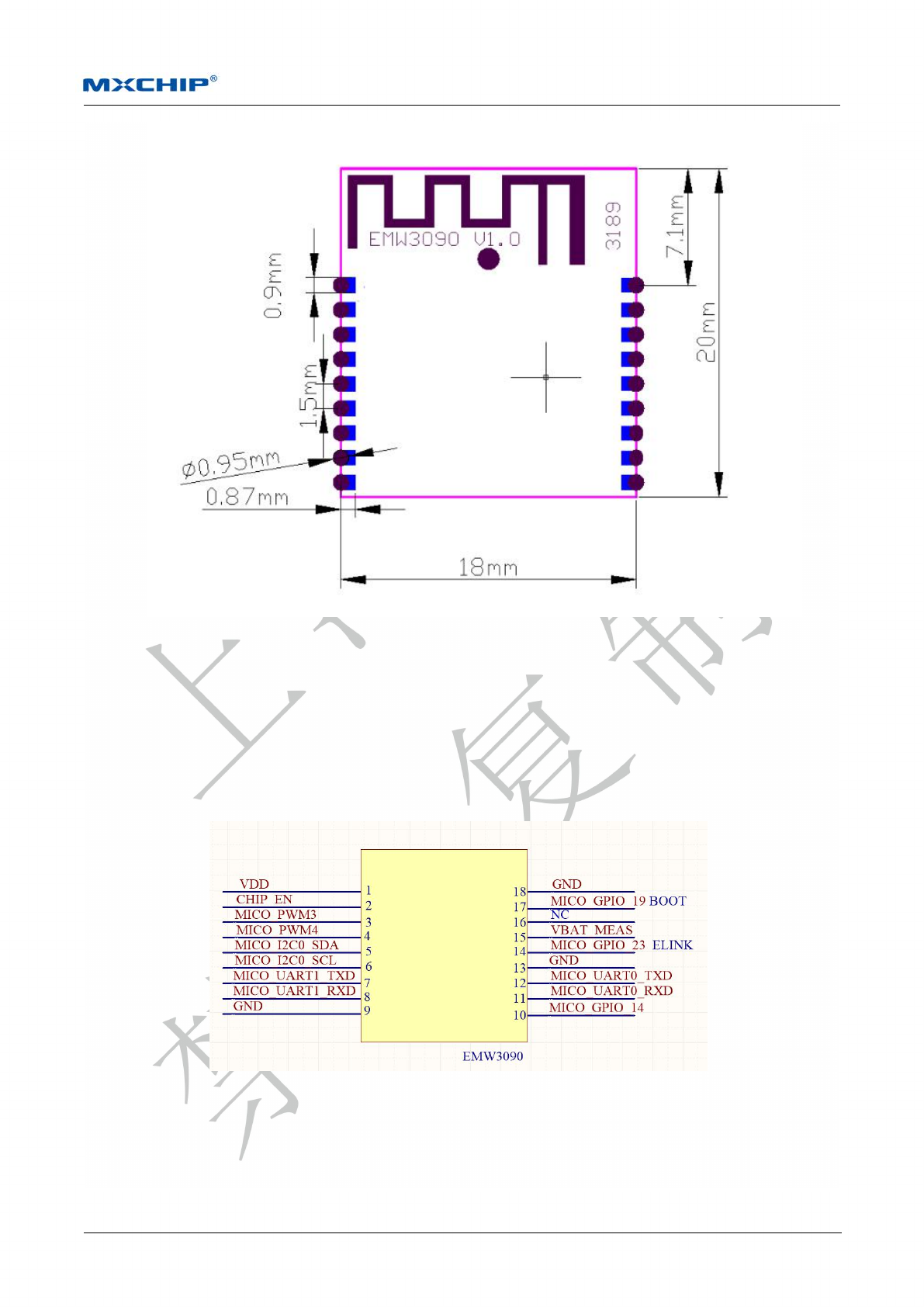
1.2 Pin Arrangement
EMW3090 has half-hole SMT package.
Solder mask openness has the same size with land. The width of steel mesh is suggested to be 0.12mm to
0.14mm in SMT.
Datasheet [Page 6]
EMW3090
Figure 2 Half-hole SMT Package Size
1.3 Pin Definition
1.3.1 EMW3090 Package Definition
Figure 3 EMW3090 Package Definition
Datasheet [Page 7]
EMW3090
1.3.2 EMW3090 Pin Definition
Table 1 EMW3090 Pin Definition
Pin
NO.
FUNCTION1
FUNCTION2
FUNCTION3
FUNCTION4
FUNCTION5
1
VDD
2
CHIP_EN
3
MICO_GPIO_12
MICO_PWM3
4
MICO_GPIO_13
MICO_PWM4
5
MICO_GPIO_8
MICO_I2C0_SDA
MICO_UART0_CTS
MICO_SPI1_CS
6
MICO_GPIO_7
MICO_I2C0_SCL
MICO_UART0_RTS
MICO_PWM6
MICO_SPI1_MISO
7
MICO_GPIO_21
MICO_I2C0_SDA
MICO_UART1_TXD
MICO_PWM4
8
MICO_GPIO_22
MICO_I2C0_SCL
MICO_UART1_RXD
MICO_PWM5
9
GND
10
MICO_GPIO_14
MICO_PWM5
11
MICO_GPIO_10
MICO_I2C1_CLK
MICO_UART0_RXD
MICO_SPI1_CLK
12
MICO_GPIO_9
MICO_I2C1_SDA
MICO_UART0_TXD
MICO_PWM1
MICO_SPI1_MOSI
13
GND
14
MICO_GPIO_23
15
VBAT_MEAS
16
NC
17
MICO_GPIO_19
18
GND
Notes:
(1) PIN 17 is used as BOOT,PIN14 is used as EASYLINK, please do not use pin 7 and 8 in hardware
design. Please contact engineer of MXCHIP if it is necessary to use the two pins.
(2) PIN7/8 should be in high voltage or NC when power on, please aware it when designing circuit.
(3) If not used, please set the pin as NC, especially for CHIP_EN.
Datasheet [Page 8]
EMW3090
2. Electrical Parameters
2.1 Operating Conditions
EMW3090 would be unstable when input voltage is less than the lowest rated voltage.
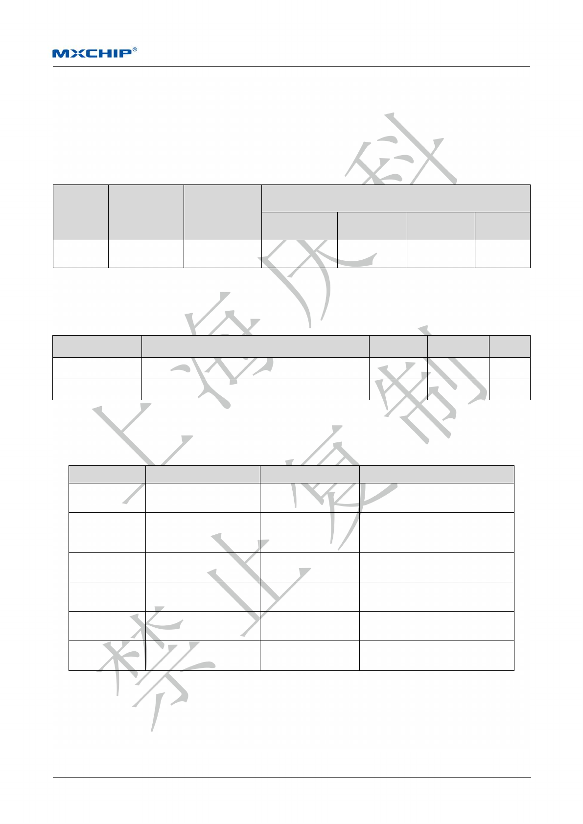
Table 2 Range of input voltage
Symbol
Illustration
Condition
Details
Minimum
Typ
Maximum
Unit
VDD
Power Supply
3.0
3.3
3.6
V
There would be permanent damage in hardware if the device operates at the voltage over rated value.
Meanwhile, reliability could be influenced when the device has a long-term operating at maximum voltage.
Table 3 Absolute maximum voltage rating
Symbol
Description
Minimum
Typ
Unit
VDD
Module input voltage
–0.3
3.6
V
VIN
GPIO input voltage
−0.3
3.6
V
2.2 Power Consumption
Table 4 EMW3090 Power Consumption
Status
Average current(3V3)
Max current(3V3)
Description
WIFI Initialization
26.91mA
33.1mA
WIFI low power mode enabled
WIFI Connected
47.71mA
119.5mA
Keep connected with the router
WIFI low power mode enabled
UDP transmission
168.37mA
298.7mA
WIFI low power mode disabled
SoftAP
121.48mA
260.4mA
SoftAP connect to internet
Easylink
122.84mA
136.7mA
Process of module network distribution
Standby
10.45uA
12.07uA
Ultra low standby power mode
Actual working current is variable at different operating mode. Maximum operating current 300 mA 。
Datasheet [Page 9]
EMW3090
2.3 Working Environment
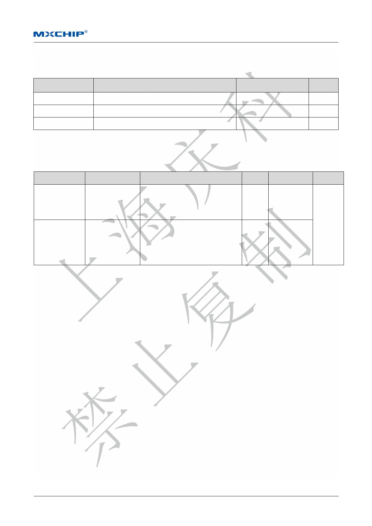
Table 5 Temperature and humidity condition
Symbol
Name
Maximum
Unit
TSTG
Storage Temperature
-20 to +85
℃
TA
Operation Temperature
-20 to +85
℃
Humidity
Non-condensing, Relative humidity
95
%
2.4 Electrostatic Discharge
Table 6 Electrostatic Discharge Parameters
Symbol
Name
Details
Level
Maximum
Unit
VESD(HBM)
Electrostatic discharge
voltage
(Human Body Model)
TA= +25 °C , JESD22-A114
2
2000
V
VESD(CDM)
Electrostatic discharge
voltage
(Charged Device
Model)
TA = +25 °C , JESD22-C101
II
500
Datasheet [Page 10]
EMW3090
3. RF parameters
3.1 Basic RF parameters
Table 7 Radio-frequency standards
Name
Illustration
Working frequency
2.412~2.472GHz
Wi-Fi wireless standard
IEEE802.11b/g/n
Data
transmission rate
20MHz
11b:1,2,5.5 和11Mbps
11g : 6,9,12,18,24,36,48,54Mbps
11n : MCS0~7,72.2Mbps
40MHz
11n:MCS0~7,150Mbps
Antenna type
PCB (Default)
IPX (Optional)
Datasheet [Page 11]
EMW3090
4. Antenna Information
4.1 Antenna Type
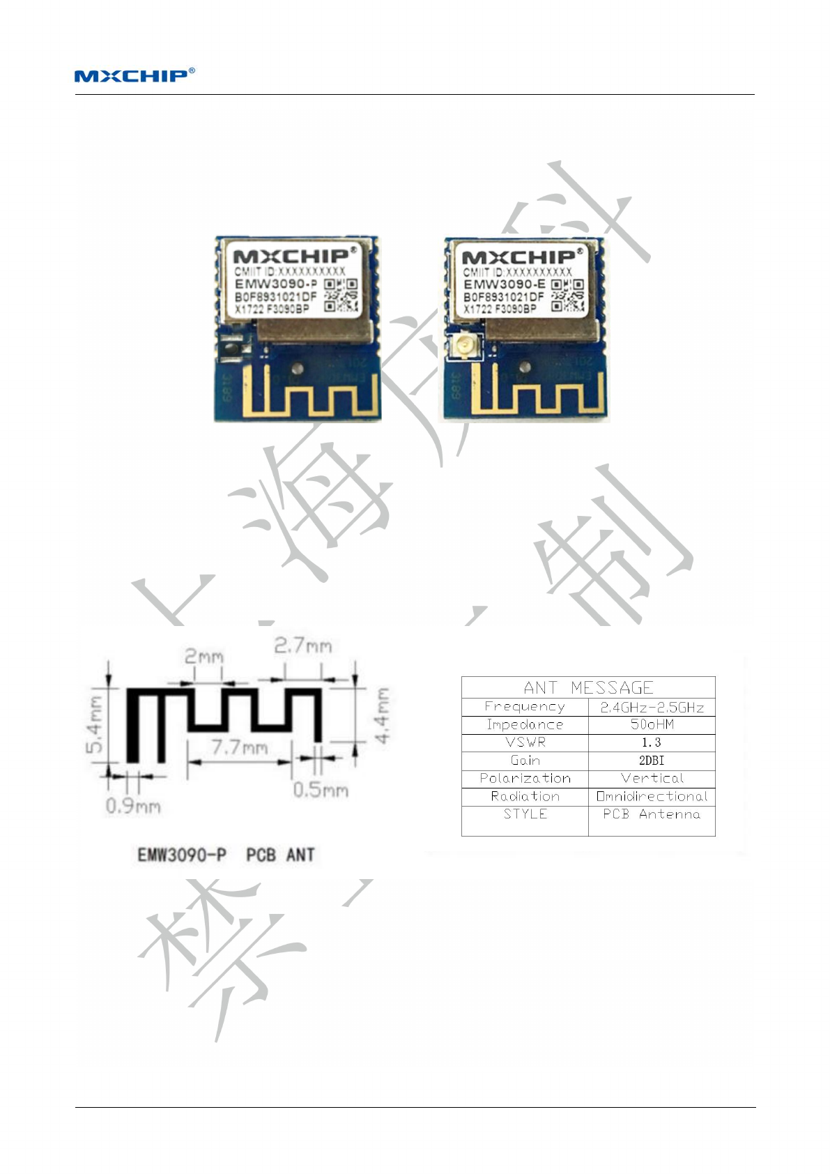
EMW3090 has two type of antenna: EMW3090-P and EMW3090-E
EWM3090-P EMW3090-E
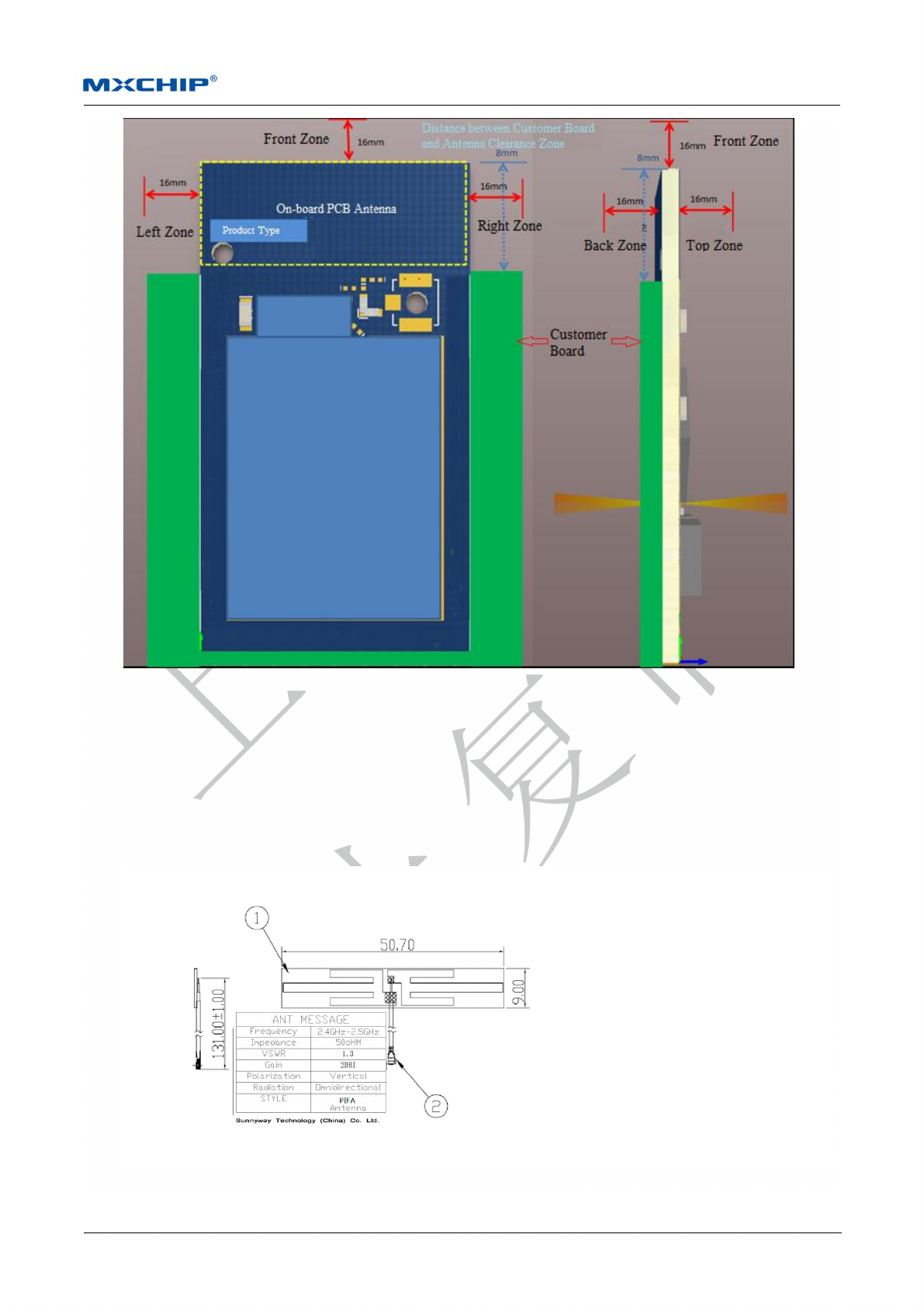
4.2 PCB Antenna Clearance Zone&PCB ANT parameter
Main PCB should have a distance over 16mm with other metal elements when using PCB antenna in Wi-Fi
device. Shadow parts in the figure below should keep away from metal elements, sensor, interference source and
other material that could cause signal interference.
Datasheet [Page 12]
EMW3090
Figure 4 Minimum Clearance Zone of PCB Antenna (Unit: mm)
4.3 External Antenna Connector&External antenna parameters
1、External Antenna Parameter:
Model name:IPEX1.3-2.4G-L131
2、External Antenna Connector
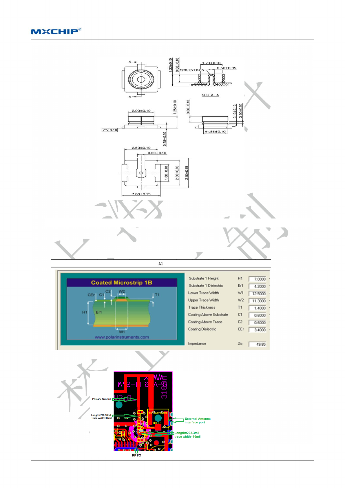
Datasheet [Page 13]
EMW3090
Figure
5
Size
of
External
Antenna
Connector
3、antenna
trace
design
The characteristic impedance depends on the dielectric of PCB, the track width and the Ground
plane spacing. Microstrip type is required. The detail simulation as below.
The RE trace of the test board which was used in the FCC test is defined as below.
Datasheet [Page 14]
EMW3090
5. Production Guidance(Important)
The stamp hole package module produced by Mxchip must completely being patched by SMT machine
in 24 hours after open firmware package. Otherwise the module should be re-package by vacuum pumping
and drying before patch.
Devices for SMT patch:
(1)Reflow soldering machine
(2)AOI detector
(3)Suction nozzle with 6-8mm caliber
Device for drying:
(1)Cabinet type oven
(2)Anti-static and high thermos tolerant tray
(3)Anti-static and high thermos tolerant gloves
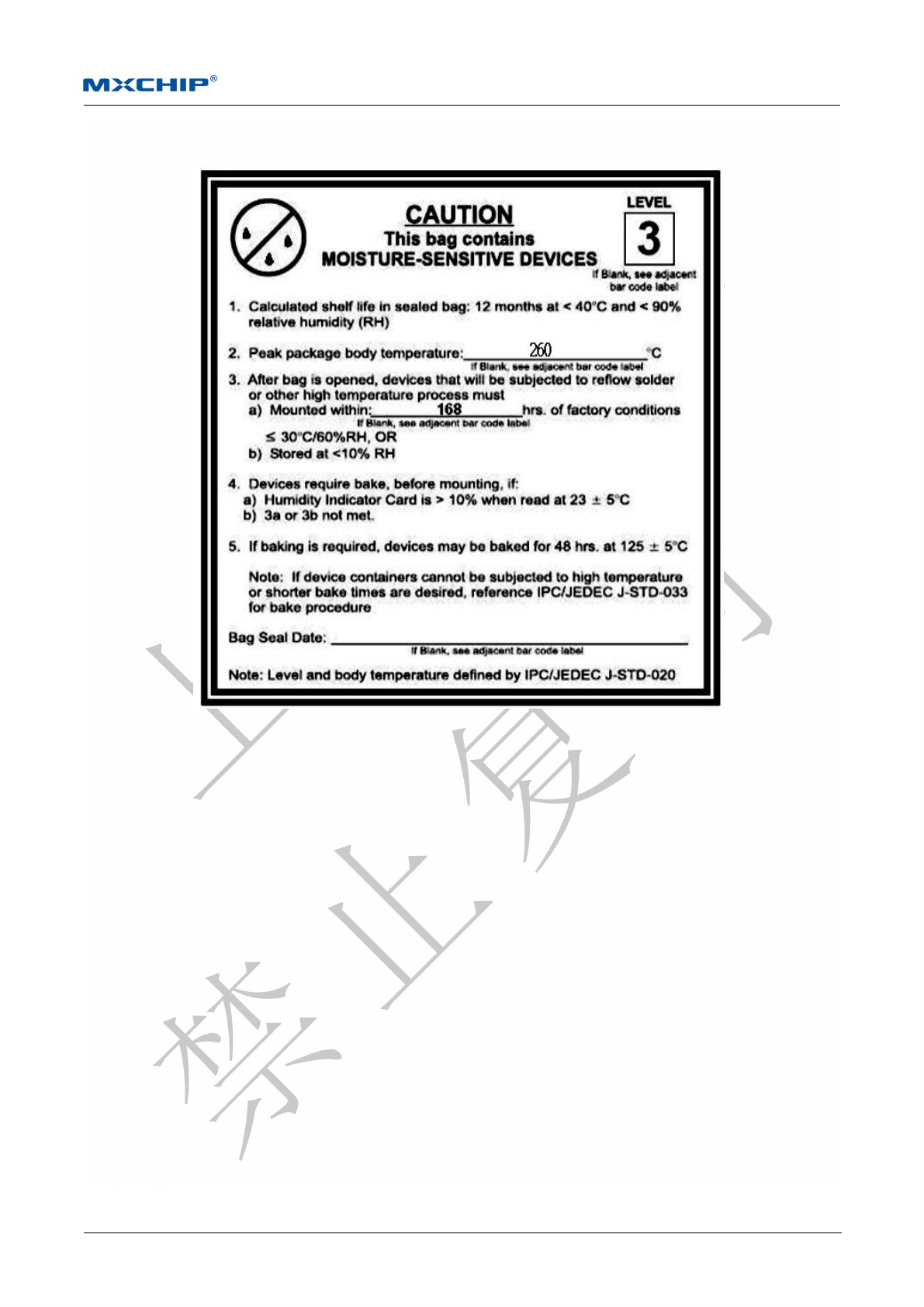
Conditions of product storage (Storage environment is shown in figure 8):
Moisture bag must be stored in temperature below 30 and humidity less than 85%RH.
Dry packaging products, the guarantee period should be from 6 months date of packing seal.
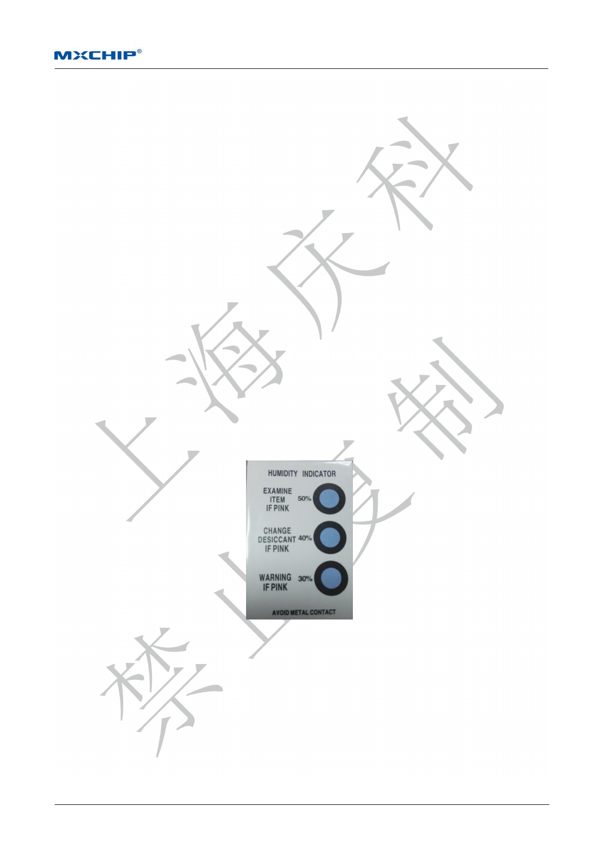
Humidity indicator card is in the hermetic package.
Figure 6 Humidity Card
Humidity indicator card and drying situation:
2 hours drying for module if the color ring at 30%, 40%, 50% in humidity indicator card is blue
after unpacking;
4 hours drying for module if the color ring at 30% in humidity indicator card is pink after
unpacking;
6 hours drying for module if the color ring at 30%, 40% in humidity indicator card is pink after

Datasheet [Page 15]
EMW3090
unpacking;
12 hours drying for module if the color ring at 30%, 40%, 50% in humidity indicator card is pink
after unpacking.
Drying parameters:
Drying temperature: 125℃±5℃;
Alarm temperature: 130℃;
SMT patch when the device cool down below 36℃in natural condition;
Dry times: 1;
Please dry again if the module is unsoldering in 12 hours after last drying.
SMT is unsuitable if the module packed over 3 months. There would be serious oxidation of the pad
because of immersion gold and cause false welding and lack of weld. Mxchip does not assume the
corresponding responsibility;
ESD protection is required before SMT;
SMT patch should on the basis of reflow profile diagram, maximum temperature 245℃, reflow profile
diagram is shown in figure 10;
In order to guarantee the reflow soldering qualification rate, vision and AOI detection should be done in
10% products for the first patch to make sure the rationality of temperature control, device adsorption mode
and position. Detect 5 to 10 sample every hour in the following batch production.
5.1 Considerations
Operator should wear anti-static gloves during producing;
No more than drying time;
Any explosive, flammable and corrosive material is not allowed to add in drying;
Module should be put into oven with high thermotolerant tray. Ventilation should exist between each
module and no direct contact with oven;
Make sure oven is closed when drying to prevent temperature leaking;
Reduce opening time or keep closing the door of the oven during drying;
Use anti-static glove to take out module when its temperature below 36℃by natural cool down after
drying;
Make sure no water and dirt in the bottom of the module;
Temperature and humidity control is level 3 for initial modules. Storage and drying conditions are based
on IPC/JEDEC J-STD-020.
Datasheet [Page 16]
EMW3090
5.2 Storage Condition
Figure 7 Storage Condition
Datasheet [Page 17]
EMW3090
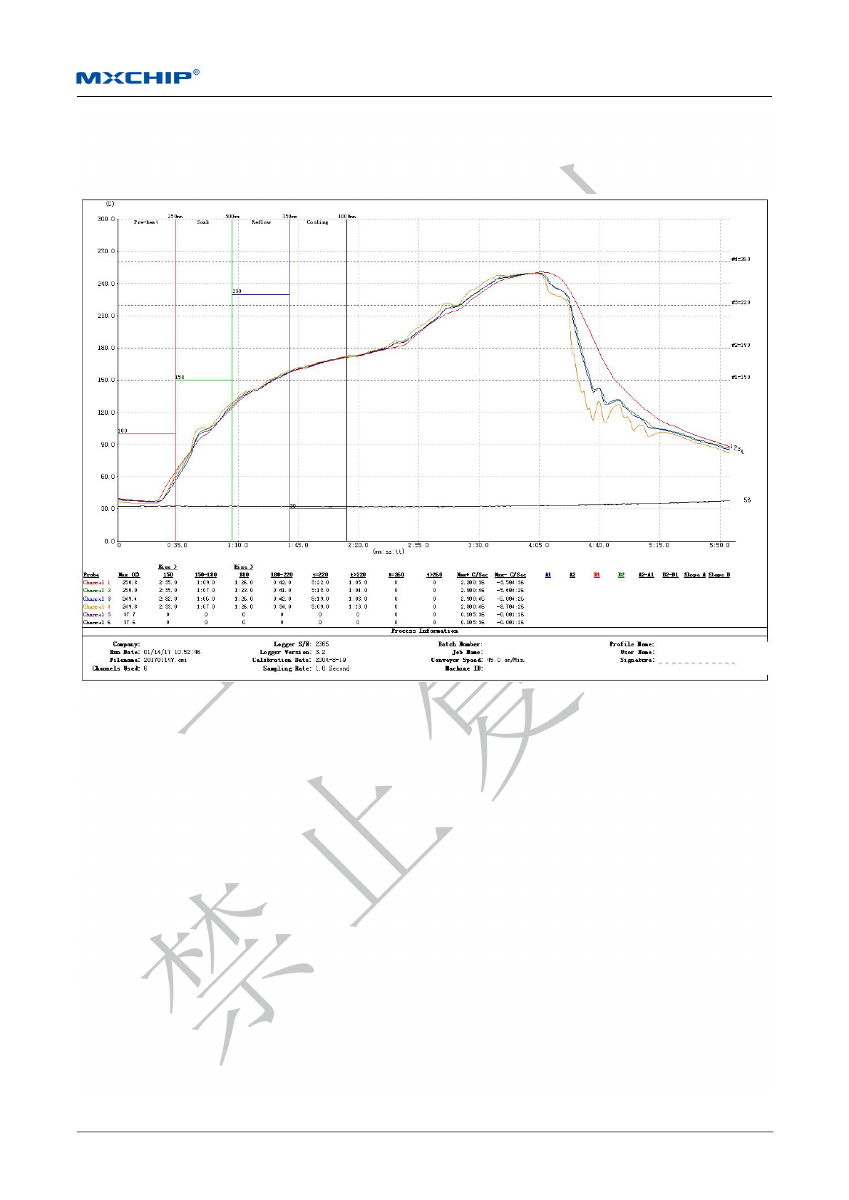
5.3 Temperature Curve of Secondary Reflow
Suggested solder paste type: SAC305, unleaded, solder paste thickness from 0.12 to 0.15, less than 2 times
reflow.
Figure 8 Temperature Curve of Secondary Reflow
Datasheet [Page 18]
EMW3090
6. Reference Circuit
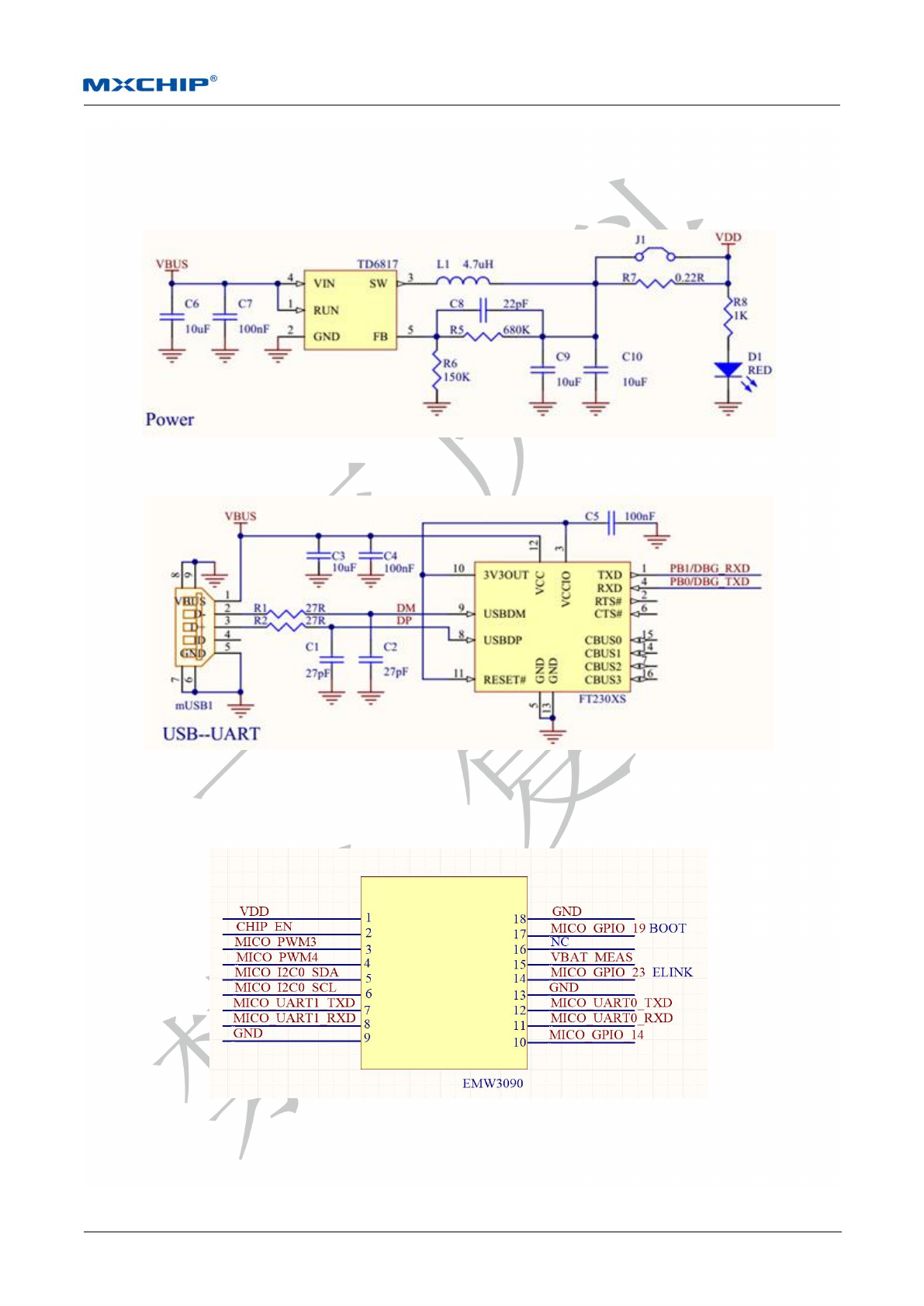
Power source circuit is shown in figure 9, USB to UART is shown in figure 10, external interface circuit is
shown in figure 11.
Figure 9 Power Source Circuit
Figure 10 USB to UART
Figure 11 External Interface Circuit of EMW3090
Datasheet [Page 19]
EMW3090
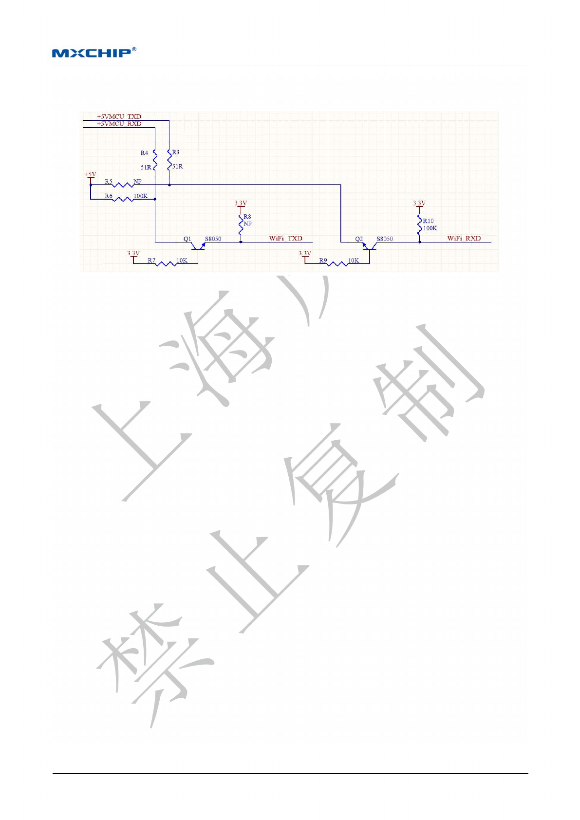
Voltage of EMW3090 UART is 3.3V. 5V UART should convert to 3.3V UART for the users that have 5V
chips. Convert circuit is shown in figure 14.
Figure 12 3.3V UART- 5V UART Convert Circuit

Datasheet [Page 20]
EMW3090
7. Sales Information and Technical Support
For consultation or purchase the product, please contact Mxchip during working hours:
From Monday to Friday, morning 9:00~12:00, afternoon 13:00~18:00
Telephone: +86-21-52655026
Contact address: 9thFloor, No.5, Lane2145 JinshaJiang Road Putuo District, ShangHai.
Postcode:200333
Email: sales@mxchip.com

Datasheet [Page 1]
EMW3090
FCC Regulations:
This device complies with part 15 of the FCC Rules. Operation is subject to the following two
conditions: (1) This device may not cause harmful interference, and (2) This device must accept any
interference received, including interference that may cause undesired operation.
This device has been tested and found to comply with the limits for a Class B digital device ,
pursuant to Part 15 of the FCC Rules. These limits are designed to provide reasonable protection
against harmful interference in a residential installation. This equipment generates, uses and can
radiated radio frequency energy and, if not installed and used in accordance with the instructions,
may cause harmful interference to radio communications. However, there is no guarantee that
interference will not occur in a particular installation If this equipment does cause harmful
interference to radio or television reception, which can be determined by turning the equipment off
and on, the user is encouraged to try to correct the interference by one or more of the following
measures:
-Reorient or relocate the receiving antenna.
-Increase the separation between the equipment and receiver.
-Connect the equipment into an outlet on a circuit different from that to which the receiver is
connected.
-Consult the dealer or an experienced radio/TV technician for help.
Caution: Changes or modifications not expressly approved by the party responsible for
compliance could void the user‘s authority to operate the equipment.
RF Exposure Information
This device complies with FCC radiation exposure limits set forth for an uncontrolled
environment. In order to avoid the possibility of exceeding the FCC radio frequency exposure limits,
human proximity to the antenna shall not be less than 20cm (8 inches) during normal operation.
IMPORTANT NOTE:
This module is intended for OEM integrator. The OEM integrator is still responsible for the FCC
compliance requirement of the end product, which integrates this module. 20cm minimum distance
has to be able to be maintained between the antenna and the users for the host this module is
integrated into. Under such configuration, the FCC radiation exposure limits set forth for an
population/uncontrolled environment can be satisfied.
Any changes or modifications not expressly approved by the manufacturer could void the user's
authority to operate this equipment.

Datasheet [Page 2]
EMW3090
USERS MANUAL OF THE END PRODUCT:
In the users manual of the end product, the end user has to be informed to keep at least 20cm
separation with the antenna while this end product is installed and operated. The end user has to be
informed that the FCC radio-frequency exposure guidelines for an uncontrolled environment can be
satisfied. The end user has to also be informed that any changes or modifications not expressly
approved by the manufacturer could void the user's authority to operate this equipment. If the size of
the end product is smaller than 8x10cm, then additional FCC part 15.19 statement is required to be
available in the users manual: This device complies with Part 15 of FCC rules. Operation is subject to
the following two conditions: (1) this device may not cause harmful interference and (2) this device
must accept any interference received, including interference that may cause undesired operation.
LABEL OF THE END PRODUCT:
The final end product must be labeled in a visible area with the following " Contains Transmitter
Module FCC ID: P53-EMW3090 ". If the size of the end product is larger than 8x10cm, then the
following FCC part 15.19 statement has to also be available on the label: This device complies with
Part 15 of FCC rules.
Operation is subject to the following two conditions: (1) this device may not cause harmful
interference and (2) this device must accept any interference received, including interference that
may cause undesired operation.