MXCHIP Information Technology EMW3161 Embedded WiFi module User Manual DS0005E EMW3161 v1 0
Shanghai MXCHIP Information Technology Co.,Ltd. Embedded WiFi module DS0005E EMW3161 v1 0
User Manual
1
Warning statement
FCC STATEMENT
1. This device complies with Part 15 of the FCC Rules. Operation is subject to the following
two conditions:
(1) This device may not cause harmful interference.
(2) This device must accept any interference received, including interference that may
cause undesired operation.
2. Changes or modifications not expressly approved by the party responsible for
compliance could void the user's authority to operate the equipment.
NOTE: This equipment has been tested and found to comply with the limits for a Class B
digital device, pursuant to Part 15 of the FCC Rules. These limits are designed to provide
reasonable protection against harmful interference in a residential installation.
This equipment generates uses and can radiate radio frequency energy and, if not installed
and used in accordance with the instructions, may cause harmful interference to radio
communications. However, there is no guarantee that interference will not occur in a
particular installation. If this equipment does cause harmful interference to radio or
television reception, which can be determined by turning the equipment off and on, the
user is encouraged to try to correct the interference by one or more of the following
measures:
Reorient or relocate the receiving antenna.
Increase the separation between the equipment and receiver.
Connect the equipment into an outlet on a circuit different from that to which the
receiver is connected.
Consult the dealer or an experienced radio/TV technician for help.
FCC Radiation Exposure Statement
This equipment complies with FCC radiation exposure limits set forth for an uncontrolled
environment. This equipment should be installed and operated with minimum distance
20cm between the radiator & your body.
The EMW3161 module is designed to comply with the FCC statement. FCC ID is
P53-EMW3161. The host system using EMW3161, should have label indicated FCC ID
P53-EMW3161.
EMW3161 embedded Wi-Fi module
Overview
EMW3161 is an ultra-compact, low-power
embedded Wi-Fi module based on MX1081, a fully
integrated System-on-Chip that is fully compatible
with Broadcom WICED platform. MX1081
integrates a wireless LAN MAC/baseband /radio,
and a Cortex-M3 microcontroller STM32F205 that
runs a unique "self-hosted" Wi-Fi networking
library and software application stack. EMW3161
has 1M bytes flash, 128k RAM and rich peripherals
for your embedded Wi-Fi applications.
EMW3161 is also an mxchipWNetTM
compatible platform, users can build their own
embedded Wi-Fi applications based on
mxchipWNetTM library which manage all of the
Wi-Fi MAC and TCP/IP stack processing. We also
provide several mxchipWNetTM firmware to meet
typical applications: wireless UART, wireless audio,
wireless sensor etc.
When using mxchipWNetTM -DTU firmware,
you can establish Wi-Fi networking for any device
with a micro-controller and a UART interface.
Quick development cycles enables fast time to
market.
Applications
Building Automation / Access Control
Smart home appliances
Medical/Health Care
Industrial Automation Systems
Point Of Sale system (POS)
Auto electronics
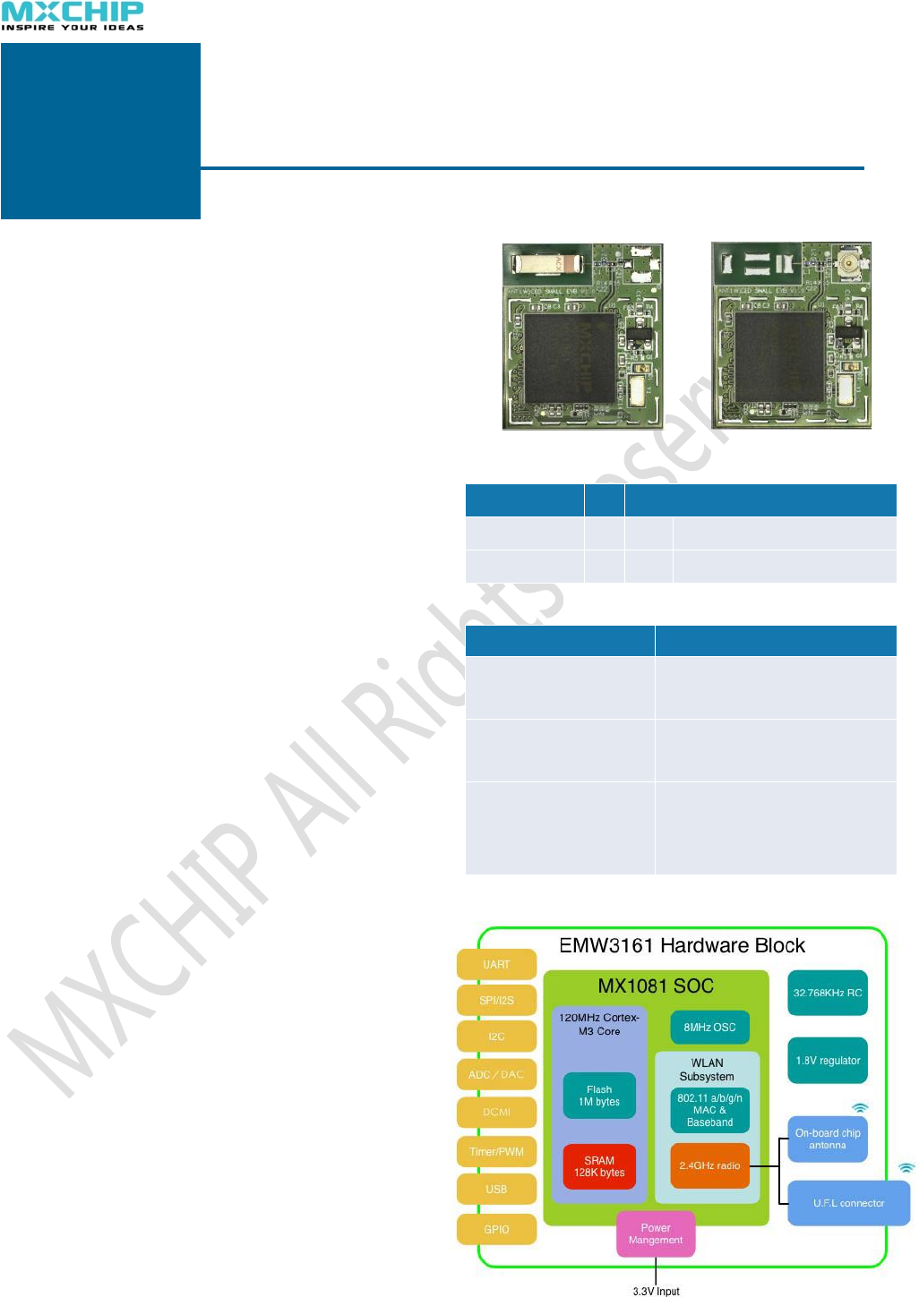
Product list
Module
-
Antenna
EMW3161
-
C
On-board chip antenna
-
E
IPEX connector
Firmware/Library
Function
mxchipWNetTM -
DTU
Predefined firmware:
UART/Wi-Fi conversion
mxchipWNetTM
Library
Software library used to
develop custom firmware
WICEDTM Firmware
development kit
WICEDTM source codes
with TCP/IP, Wi-Fi MAC
RTOS and GCC tool chain
Hardware block
MXCHIP Co., Ltd
Data Sheet
EMW3161
Embedded Wi-Fi module
2.0
Date:2013-07-17
Data Sheet
2
Contents
1 INTRODUCTION .......................... 1
Features ................................................... 2
2 INTERFACE ................................... 3
Pinouts ..................................................... 3
Pin Arrangement .................................... 3
Pin Arrangement for peripherals ......... 8
Typical Pin Arrangement ....................... 9
3 ELECTRICAL PARAMETERS ....... 10
Absolute maximum ratings: ............... 10
3.1.1 Voltage & Current .................................................. 10
Operating conditions: .......................... 10
3.2.1 Voltage & Current .................................................. 10
Digital I/O port characteristics ........... 13
3.3.1 Output voltage levels ............................................ 13
3.3.2 Output voltage levels ............................................ 14
3.3.3 nRESET pin characteristics ................................... 14
Other MCU electrical parameters ....... 14
Temperature and Humidity ................. 14
ESD ......................................................... 15
Static latch-up ....................................... 15
RF characteristics ................................. 15
3.8.1 Basic RF characteristics ......................................... 15
3.8.2 IEEE802.11b mode .................................................. 16
3.8.3 IEEE802.11g mode .................................................. 16
3.8.4 IEEE802.11n 20MHz bandwidth mode ............ 17
Mechanical Dimensions ...................... 19
3.9.1 EMW3161 Mechanical Dimensions .................. 19
4 ANTENNA INFORMATION ....... 20
Minimizing radio interference ........... 20
U.F.L RF Connector ............................... 21
5 OTHERS ...................................... 22
Recommended Reflow Profile ............ 22
MSL/Storage Condition ....................... 22
6 SALES INFORMATION .............. 23
7 TECHNICAL SUPPORT .............. 23
1
1 Introduction
EMW3161 is an ultra-compact, low-power embedded Wi-Fi module based on
MX1080, a fully integrated System-on-Chip that is fully compatible with Broadcom
WICED platform. MX1081 integrates a Broadcom BCM43362 wireless LAN
MAC/baseband/radio, and an embedded processor core that runs a unique "self-hosted"
Wi-Fi networking library and software application stack. EMW3161 has 1M bytes flash,
128k RAM and rich peripherals for your embedded Wi-Fi applications.
EMW3161 is also an mxchipWNetTM compatible platform, users can build their own
embedded Wi-Fi applications based on mxchipWNetTM library which manage all of the
Wi-Fi MAC and TCP/IP stack processing. We also provide several mxchipWNetTM
firmware to meet typical applications: wireless UART, wireless audio, wireless sensor etc.
When using mxchipWNetTM-DTU firmware, you can establish Wi-Fi networking for
any device with a micro-controller and a serial interface. Quick development cycles
enables fast time to market.

2
1.1 Features
Single operation voltage:3.3V
Power consumption: <130mA under running mode, <1mA under standby mode.
STM32F2 MCU frequency: 120MHz,flash size: 1M bytes,RAM size128k bytes.
On-chip functionality Single-chip: MAC/BB/RF
Peripherals:
42 x GPIOs
3 x UARTs,UART2 include hardware flow control
2 x SPI, 1xIIS
8 x ADC input channels,2 DAC output channel
1 x USB device, 1 x CAN
2 x I2C
PWM/Timer input/output
DCMI
SWD debug interface
Wi-Fi connectivity
802.11b, 802.11g, 802.11n (single stream) on channel 1-14@2.4GHz
WEP, WPA/WPA2 PSK/Enterprise
Transmit power:18.5dBm@11b,15.5dBm@11g,14.5dBm@11n
MIN Receiver Sensitivity: -96 dBm
Max Data rate:11Mbps@11b,54Mbps@11g,72Mbps@11n HT20
Wi-Fi modes:Station, Soft AP and Wi-Fi direct
Advanced 1x1 802.11n features
Full/Half Guard Interval
Frame Aggregation
Space Time Block Coding (STBC)
Low Density Parity Check (LDPC) Encoding
Hardware Encryption: WEP, WPA/WPA2
WPS 2.0
Multiple power save modes
On-board chip antenna,IPEX connector for external antenna
CE,FCC compliant
Operating Temperature: -40℃ to 85℃
MSL level 3
3
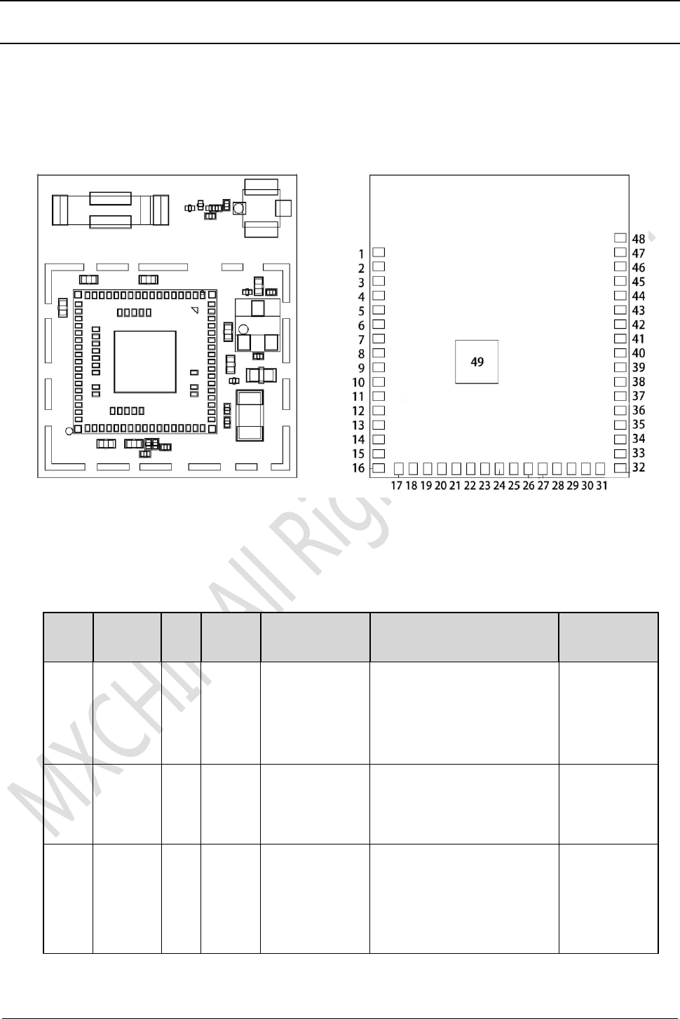
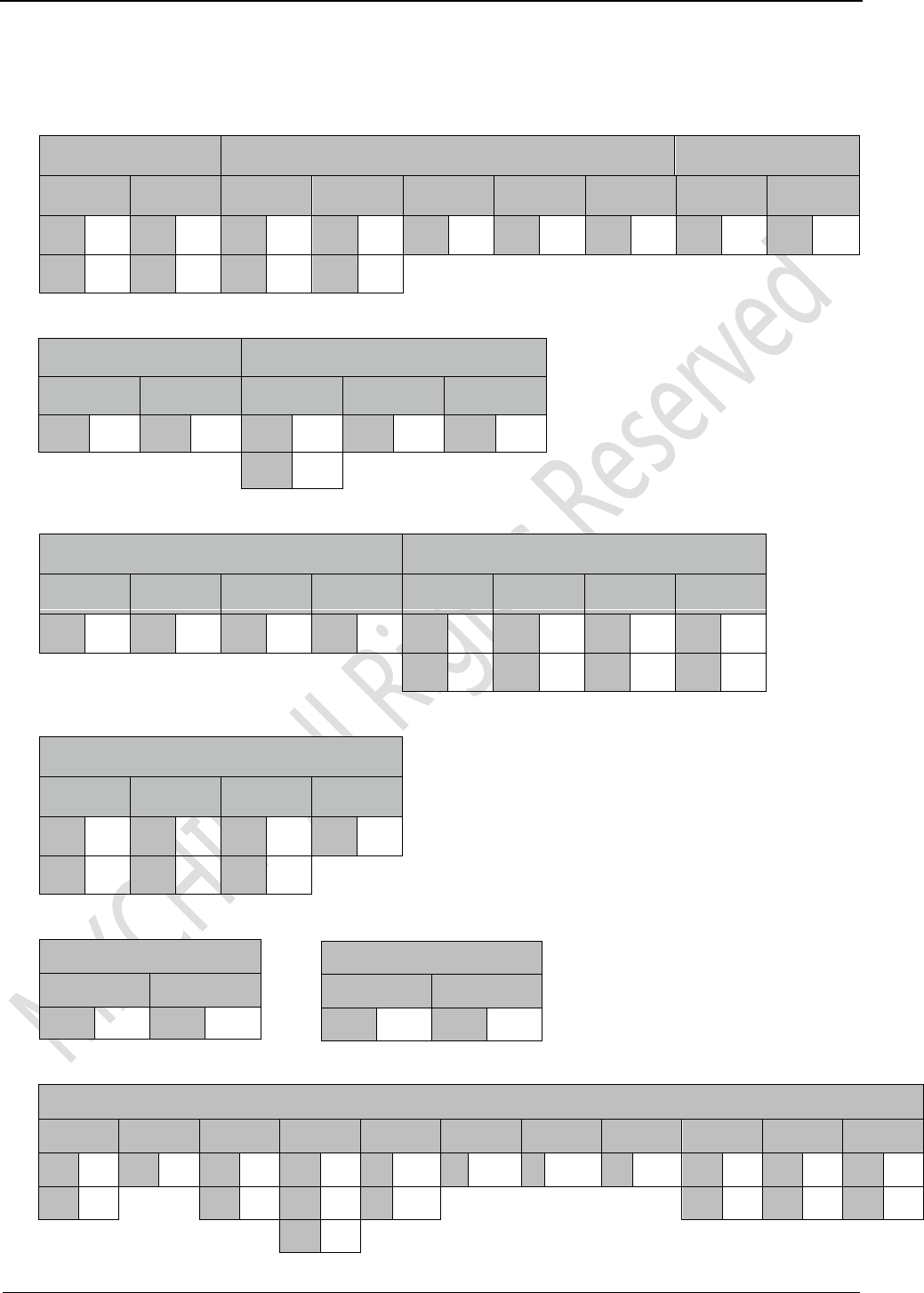
2 Interface
2.1 Pinouts
EMW3161 has two groups of pins (1X15 +1X15). The lead pitch is 2mm.
EMW3161’s pinout is shown in the Figure 2.1. Table 2.2 lists the pin functions.
Figure2.1 EMW3161: appearance and pinout
2.2 Pin Arrangement
Figure 2.2 EMW3161 pin arrangement
Pins
Name
Type
IO level
Main function
(after reset)
Alternate functions
Other
functions
1
PA4(2)
I/O
TT
PA4
SPI1_NSS / SPI3_NSS /
USART2_CK / DCMI_HSYNC
/ OTG_HS_SOF/ I2S3_WS/
EVENTOUT
ADC12_IN4
/DAC1_OUT
2
PA5(2)
I/O
TT
PA5
SPI1_SCK/ OTG_HS_ULPI_CK
/ TIM2_CH1_ETR/
TIM8_CHIN/ EVENTOUT
ADC12_IN5
/DAC2_OUT
3
PA6(2)
I/O
FT
PA6
SPI1_MISO /
TIM8_BKIN/TIM13_CH1 /
DCMI_PIXCLK / TIM3_CH1 /
TIM1_BKIN/ EVENTOUT
ADC12_IN6

4
Pins
Name
Type
IO level
Main function
(after reset)
Alternate functions
Other
functions
4
PA7(2)
I/O
FT
PA7
SPI1_MOSI/ TIM8_CH1N /
TIM14_CH1 TIM3_CH2/
ETH_MII_RX_DV /
TIM1_CH1N / RMII_CRS_DV
/ EVENTOUT
ADC12_IN7
5
PB14
I/O
FT
PB14
SPI2_MISO/ TIM1_CH2N /
TIM12_CH1 / OTG_HS_DM
USART3_RTS/ TIM8_CH2N/
EVENTOUT
6
PB15
I/O
TT
PB15
SPI2_MOSI / I2S2_SD /
TIM1_CH3N / TIM8_CH3N /
TIM12_CH2 / OTG_HS_DP /
RTC_50Hz/ EVENTOUT
7
PB10
I/O
FT
JTDO/
TRACESWO
SPI2_SCK/ I2S2_SCK/
I2C2_SCL / USART3_TX /
OTG_HS_ULPI_D3 /
ETH_MII_RX_ER /
TIM2_CH3/ EVENTOUT
8
PB12
I/O
FT
PB12
SPI2_NSS/I2S2_WS/
I2C2_SMBA/ USART3_CK/
TIM1_BKIN / CAN2_RX /
OTG_HS_ULPI_D5/
ETH_RMII_TXD0 /
ETH_MII_TXD0/ OTG_HS_ID/
EVENTOUT
9
PC6
I/O
FT
PC6
I2S2_MCK /
TIM8_CH1/SDIO_D6 /
USART6_TX /
DCMI_D0/TIM3_CH1/
EVENTOUT
10
PH8
I/O
FT
PH8
I2C3_SDA / DCMI_HSYNC/
EVENTOUT
11
PH9
I/O
FT
PH9
I2C3_SMBA / TIM12_CH2/
DCMI_D0/ EVENTOUT
12
PH10
I/O
FT
PH10
TIM5_CH1 / DCMI_D1/
EVENTOUT
13
PH11
I/O
FT
PH11
TIM5_CH2 / DCMI_D2/
EVENTOUT

5
Pins
Name
Type
IO level
Main function
(after reset)
Alternate functions
Other
functions
14
PH12
I/O
FT
PH12
TIM5_CH3 / DCMI_D3/
EVENTOUT
15
PH14
I/O
FT
PH14
TIM8_CH2N / DCMI_D4/
EVENTOUT
16
PI4
I/O
FT
PI4
TIM8_BKIN / DCMI_D5/
EVENTOUT
17
PI5
I/O
FT
PI5
TIM8_CH1 / DCMI_VSYNC/
EVENTOUT
18
PI6
I/O
FT
PI6
TIM8_CH2 / DCMI_D6/
EVENTOUT
19
PI7
I/O
FT
PI7
TIM8_CH3 / DCMI_D7/
EVENTOUT
20
PA9
I/O
FT
PA9
USART1_TX/ TIM1_CH2 /
I2C3_SMBA / DCMI_D0/
EVENTOUT
OTG_FS_ VBUS
21
PA10
I/O
FT
PA10
USART1_RX/ TIM1_CH3/
OTG_FS_ID/DCMI_D1/
EVENTOUT
22
PH13
I/O
FT
PH13
TIM8_CH1N / CAN1_TX/
EVENTOUT
23
PH15
I/O
FT
PH15
TIM8_CH3N / DCMI_D11/
EVENTOUT
24
PD5
I/O
FT
PD5
FSMC_NWE/USART2_TX/
EVENTOUT
25
PD6
I/O
FT
PD6
FSMC_NWAIT/ USART2_RX/
EVENTOUT
26
PA13
I/O
FT
JTMS- SWDIO
JTMS-SWDIO/ EVENTOUT
27
PA14
I/O
FT
JTCK- SWCLK
JTCK-SWCLK/ EVENTOUT
28
PB6
I/O
FT
PB6
I2C1_SCL/ TIM4_CH1 /
CAN2_TX /
DCMI_D5/USART1_TX/
EVENTOUT
29
PB7
I/O
FT
PB7
2C1_SDA / FSMC_NL(8) /
DCMI_VSYNC /
USART1_RX/ TIM4_CH2/
EVENTOUTDCMI_D5/USART
1_TX/ EVENTOUT

6
Pins
Name
Type
IO level
Main function
(after reset)
Alternate functions
Other
functions
30
BOOT0
I
BOOT0
31
PI2
I/O
FT
PI2
TIM8_CH4 /SPI2_MISO /
DCMI_D9/ EVENTOUT
32
PI1
I/O
FT
PI1
SPI2_SCK / I2S2_SCK /
DCMI_D8/ EVENTOUT
33
PI0
I/O
FT
PI0
TIM5_CH4 / SPI2_NSS /
I2S2_WS / DCMI_D13/
EVENTOUT
34
PI3
I/O
FT
PI3
TIM8_ETR / SPI2_MOSI /
I2S2_SD / DCMI_D10/
EVENTOUT
35
PE5
I/O
FT
PE5
TRACED2 / FSMC_A21 /
TIM9_CH1 / DCMI_D6/
EVENTOUT
36
PE6
I/O
FT
PE6
TRACED3 / FSMC_A22 /
TIM9_CH2 / DCMI_D7/
EVENTOUT
37
PF9(2)
I/O
FT
PF9
TIM14_CH1 / FSMC_CD/
EVENTOUT
ADC3_IN7
38
PF0
I/O
FT
PF0
FSMC_A0 / I2C2_SDA/
EVENTOUT
39
PF1
I/O
FT
PF1
FSMC_A1 / I2C2_SCL/
EVENTOUT
40
NRST
I/O
NRST
41
GND
S
GND
42
VDD
S
VDD
43
VDD
S
VDD
44
GND
S
GND
45
PA0-
WKUP(2)
I/O
FT
PA0-WKUP
USART2_CTS/ UART4_TX/
ETH_MII_CRS /
TIM2_CH1_ETR/ TIM5_CH1
/ TIM8_ETR/ EVENTOUT
ADC123_IN0/
WKUP
46
PA1(2)
I/O
FT
PA1
USART2_RTS / UART4_RX/
ETH_RMII_REF_CLK /
ETH_MII_RX_CLK /
TIM5_CH2 / TIM2_CH2/
EVENTOUT
ADC123_IN1
47
PA2(2)
I/O
FT
PA2
USART2_TX/TIM5_CH3 /
ADC123_IN2

7
Pins
Name
Type
IO level
Main function
(after reset)
Alternate functions
Other
functions
TIM9_CH1 / TIM2_CH3 /
ETH_MDIO/EVENTOUT
48
PA3(2)
I/O
FT
PA3
USART2_RX/TIM5_CH4 /
TIM9_CH2 / TIM2_CH4 /
OTG_HS_ULPI_D0 /
ETH_MII_COL/ EVENTOUT
ADC123_IN3
49
GND
S
GND
1. FT = 5 V tolerant; TT = 3.6 V tolerant.
2. FT = 5 V tolerant except when in analog mode or oscillator mode (for PC14,
PC15, PH0 and PH1).
3. I = input, O = output, S = supply.
4. STM32 peripherals are not listed if they cannot be presented on current pins
8
2.3 Pin Arrangement for peripherals
Some of STM32 peripherals are not listed if their main function is not usable on
EMW3161.
USART1(AF7)
USART2(AF7)
USART4(AF8)
TX
RX
TX
RX
CTS
RTS
CK
TX
RX
20
PA9
21
PA10
47
PA2
48
PA3
45
PA0
46
PA1
1
PA4
45
PA0
46
PA1
28
PB6
29
PB7
24
PD5
25
PD6
I2C1(AF4)
I2C2(AF4)
SCL
SDA
SCL
SDA
SMBA
28
PB6
29
PB7
39
PF1
38
PF0
8
PB12
7
PB10
SPI1(AF5)
SPI2(AF5)
NSS
SCK
MISO
MOSI
NSS
SCK
MOSI
MISO
1
PA4
2
PA5
3
PA6
4
PA7
33
PI0
32
PI1
34
PI3
31
PI2
8
PB12
7
PB10
6
PB15
5
PB14
IIS2(AF5)
WS
SCK
SD
MCK
33
PI0
32
PI1
34
PI3
9
PC6
8
PB12
7
PB10
6
PB15
USB_HS(AF12)
DP
DM
6
PB15
5
PB14
DCMI(AF13)
HSYNC
PIXCK
VSYNC
D0
D1
D2
D3
D4
D5
D6
D7
1
PA4
3
PA6
29
PB7
11
PH9
12
PH10
13
PH11
14
PH12
15
PH14
16
PI4
18
PI6
19
PI7
10
PH8
17
PI5
20
PA9
21
PA10
28
PB6
35
PE5
36
PE6
9
PC6
CAN2(AF9)
TX
RX
28
PB6
8
PB12
9
ADC123(AF14)
ADC12(AF14)
ADC3(AF14)
IN0
IN1
IN2
IN3
IN4
IN5
IN6
IN7
IN7
45
PA0
46
PA1
47
PA2
48
PA3
1
PA4
2
PA5
3
PA6
4
PA7
37
PF9
DAC1(AF14)
DAC2(AF14)
OUT
OUT
1
PA4
2
PA5
2.4 Typical Pin Arrangement
10
3 Electrical Parameters
3.1 Absolute maximum ratings:
3.1.1 Voltage & Current
Stresses above the absolute maximum ratings may cause permanent damage to the
device. These are stress ratings only and functional operation of the device at these
conditions is not implied. Exposure to maximum rating conditions for extended periods
may affect device reliability.
Symbol
Ratings
Min
Max
Unit
VDD–VSS
Voltage
–0.3
4.0
V
VIN
Input voltage on five volt tolerant pin
VSS −0.3
5.5
V
VIN
Input voltage on any other pin
VSS −0.3
VDD+0.3
V
Symbol
Ratings
Max
Unit
IVDD
Total current into VDD power lines (source)
320
mA
IVSS
Total current out of VSS ground lines (sink)
320
IIO
Output current sunk by any I/O and control pin
25
Output current source by any I/O and control pin
-25
3.2 Operating conditions
3.2.1 Voltage & Current
Symbol
Note
Conditions
Specification
Min.
Typical
Max.
Unit
VDD
Voltage
2.4
3.3
3.5
V

11
WLAN Subsystem
Symbol
Note
Conditions
Typical
Unit
IRF
OFF1
2
μA
IRF
SLEEP4
200
μA
IRF
Rx(Listen)2
52
mA
IRF
Rx(Active)3
59
mA
IRF
Power Save5 6
1.9
mA
IRF
Tx CCK7 10
11 Mbps at 18.5 dBm
320
mA
IRF
Tx OFDM8 10
54 Mbps at 15.5 dBm
270
mA
IRF
Tx OFDM9 10
65 Mbps at 14.5 dBm
260
mA
Note 1: Power is off.
Note 2: Carrier Sense (CCA) when no carrier present
Note 3: Carrier Sense (CS) detect/Packet Rx
Note 4: Intra-beacon Sleep
Note 5: Beacon Interval = 102.4ms, DTIM = 1, Beacon duration = 1 ms @1 Mbps.
Integrated Sleep + wakeup + Beacon Rx current over 1 DTIM interval.
Note 6: In WLAN power-saving mode, the following blocks are powered down:
Crystal oscillator, Baseband PLL, AFE, RF PLL, Radio
Note 7: CCK power at chip port. Duty cycle is 100%. Includes PA contribution.
Note 8: OFDM power at chip port. Duty cycle is 100%. Includes PA contribution.
Note 9: OFDM power at chip port is 16 dBm, duty cycle is 100%, includes PA
contribution.
Note 10: Absolute junction temperature limits maintained through active thermal
monitoring and dynamic Tx duty cycle limiting.
12
Microcontroller Subsystem
Typical and maximum current consumption in Run mode, code with data processing
running from Flash memory (ART accelerator enabled) or RAM
Symbol
Conditions
fHCLK
Running Mode
Sleep Mode
Unit
TA=25°C
TA=25°C
IMCU
External clock, all
peripherals enabled
120MHz
49
38
mA
90MHz
38
30
60MHz
26
20
30MHz
14
11
25MHz
11
8
16MHz
8
6
8MHz
5
3.6
4MHz
3
2.4
2MHz
2
1.9
External clock, all
peripherals disabled
120MHz
21
8
90MHz
17
7
60MHz
12
5
30MHz
7
3.5
25MHz
5
2.5
16MHz
4
2.1
8MHz
2.5
1.7
4MHz
2
1.5
2MHz
1.6
1.4
Typical and maximum current consumptions in Stop mode
Symbol
Parameter
Conditions
Typ
Max
Unit
TA=25°C
TA=25°C
IMCU
Supply current in
Stop mode with
main regulator in
Run mode
Flash in Stop mode, low-speed and
high-speed internal RC oscillators and
high-speed oscillator OFF (no
independent watchdog).
0.55
1.2
mA
Flash in Deep power down mode, low-
speed and high-speed internal RC
oscillators and high-speed oscillator OFF
(no independent watchdog).
0.5
1.2
Supply current in
Stop mode with
main regulator in
Low Power mode
Flash in Stop mode, low-speed and
high-speed internal RC oscillators and
high-speed oscillator OFF (no
independent watchdog).
0.35
1.1
Flash in Deep power down mode, low-
speed and high-speed internal RC
oscillators and high-speed oscillator OFF
(no independent watchdog).
0.3
1.1
13
Typical and maximum current consumptions in Standby mode
Symbol
Parameter
Conditions
Typ
Unit
TA=25°C
IMCU
Supply current
in Standby
mode
Backup SRAM ON, low-speed oscillator and RTC ON
4.0
μA
Backup SRAM OFF, low-speed oscillator and RTC ON
3.3
Backup SRAM ON, RTC OFF
3.0
Backup SRAM OFF, RTC OFF
2.2
Power consumption in typical operation modes3
Symbol
Parameter
Conditions
Min
Average
Max
Unit
TA=25°C
TA=25°C
TA=25°C
Imodule
Total power
consumption
on EMW3161
module
No Wi-Fi data is transmitting1
2.8
7.2
73.5
mA
Receive data in UDP mode, 20k bps1
2.8
12
262
mA
Send data in UDP mode, 20k bps1
3
24
280
mA
RF off, MCU enter standby mode2
4
6
8
μA
Connecting to AP
52
74
320
mA
Note1: TA=25°C, MCU frequency=120MHz, with data processing running from Flash
memory (ART accelerator enabled). Firmware process TCP/IP stack and IEEE 802.11 MAC
every 250 milliseconds, enter stop mode when no task is pending.
RF subsystem is connected to an access point and run under power save mode in
IEEE 802.11n@14.5 dBm Tx power. AP Beacon Interval = 102.4ms, DTIM = 1.
Note2: Wi-Fi connection is disconnected.
Note3: These data may not be the same depend on different firmware functions.
3.3 Digital I/O port characteristics
3.3.1 Output voltage levels
Symbol
Note
Parameter
Conditions
Min.
Max.
Unit
VOL
UART& IO
output voltage
Output low level voltage
IIO= +8 mA
2.7 V < VDD < 3.6 V
0.4
V
VOH
Output high level voltage
VDD-0.4
V
VOL
Output low level voltage
IIO= +20 mA
2.7 V < VDD < 3.6 V
1.3
V
VOH
Output high level voltage
VDD-1.3
V
14
3.3.2 Output voltage levels
Symbol Note Parameter Conditions Min. Max. Unit
VIL
UART& IO
input voltage
Input low level voltage
TTL level
-0.5 0.8 V
VIH
Input high level voltage 2 VDD+0.5 V
Input high level voltage
(5V input tolerant) 2 5.5 V
VIL Input low level voltage CMOS level -0.5 0.35VDD V
VIH Input high level voltage 0.65VDD VDD+0.5 V
3.3.3 nRESET pin characteristics
The nRESET pin input driver uses CMOS technology. EMW3161 contains RC
(resistance-capacitance) reset circuit which ensures the module reset accurately when it
powers up. If you need to reset manually, just connect the external control signals to the
reset pins directly, but the control signal should be Open Drain Mode。
Symbol Item Conditions Min. Typical Max. Unit
VIL(NRST) nRESET input low level –0.5 0.8 V
VIH(NRST) nRESET input high level 2 VDD+0.5
RPU Resistor for Pulling up VIN= VSS 7.5 8 8.3 kΩ
CPD Capacitor for charging and Resetting 100 1000 pF
3.4 Other MCU electrical parameters
Please refer to STM32F215RGT6 data sheet.
3.5 Temperature and Humidity
Symbol Ratings Max Unit
TSTG Storage temperature –55 to +125
℃
TA Working temperature -40 to +85
℃
Humidity Non condensing, relative humidity Max. 95%

15
3.6 ESD
Absolute maximum ratings: The Electromagnetic Environment Electrostatic discharge
Symbol Ratings Conditions Class Max Unit
VESD(HBM) Electrostatic discharge voltage
(human body model)
TA= +25 °C
conforming to
JESD22-A114
2 2000
V
VESD(CDM) Electrostatic discharge voltage
(charge device model)
TA = +25 °C
conforming to
JESD22-C101
II 500
3.7 Static latch-up
These tests are compliant with EIA/JESD 78A IC latch-up standard.
Symbol Parameter Class Class
LU Static latch-up class TA= +105 °C conforming to JESD78A II level A
3.8 RF characteristics
3.8.1 Basic RF characteristics
Item Specification
Operating Frequency FCC:2412~2462MHz CE:2412-2472MHz
Wi-Fi Standard 802.11b/g/n(single stream n)
Modulation Type
11b: DBPSK, DQPSK,CCK for DSSS
11g: BPSK, QPSK, 16QAM, 64QAM for OFDM
11n: MCS0~7,OFDM*
Data Rates
11b:1, 2, 5.5 and 11Mbps
11g:6, 9, 12, 18, 24, 36, 48 and 54 Mbps
11n: MCS0~7, up to 72Mbps
Antenna type One U.F.L connector for external antenna
PCB printed ANT (Reserve)
16
3.8.2 IEEE802.11b mode
Item Specification
Modulation Type DSSS / CCK
Frequency range FCC:2412MHz~2462MHz CE:2412MHz-2472MHz
Channel CH1 to CH14
Data rate 1, 2, 5.5, 11Mbps
TX Characteristics Min. Typical Max. Unit
Transmitter Output Power
11bTarget Power 18.5 dBm
Spectrum Mask @ target power
fc +/-11MHz to +/-22MHz -30 dBr
fc > +/-22MHz -50 dBr
Frequency Error -20 +20 ppm
Constellation Error( peak EVM)@ target power
1~11Mbps
-17 -10
RX Characteristics Min. Typical Max. Unit
Minimum Input Level Sensitivity
1Mbps (FER≦8%) -97 -83 dBm
2Mbps (FER≦8%) -93 -80 dBm
5.5Mbps (FER≦8%) -91 -79 dBm
11Mbps (FER≦8%) -89 -76 dBm
Maximum Input Level (FER≦8%) -10 dBm
3.8.3 IEEE802.11g mode
Item Specification
Modulation Type OFDM
Frequency range 2400MHz~2484MHz
Channel CH1 to CH14
Data rate 6, 9, 12, 18, 24, 36, 48, 54Mbps
TX Characteristics Min. Typical Max. Unit
Transmitter Output Power
17
11gTarget Power
15.5
dBm
Spectrum Mask @ target power
fc +/-11MHz
-20
dBr
fc +/-20MHz
-28
dBr
fc > +/-30MHz
-40
dBr
Frequency Error
-20
+20
ppm
Constellation Error( peak EVM)@ target power
6Mbps
-5
dB
9Mbps
-8
dB
12Mbps
-10
dB
18Mbps
-13
dB
24Mbps
-16
dB
36Mbps
-19
dB
48Mbps
-22
dB
54Mbps
-30
-25
dB
Transmit spectrum mask
@ 11MHz
-20
dBr
@ 20MHz
-28
dBr
@ 30MHz
-40
dBr
RX Characteristics
Min.
Typical
Max.
Unit
Minimum Input Level Sensitivity
6Mbps (FER
≦
10%)
-90
-82
dBm
9Mbps (FER
≦
10%)
-88
-87
dBm
12Mbps (FER
≦
10%)
-86
-79
dBm
18Mbps (FER
≦
10%)
-85
-77
dBm
24Mbps (FER
≦
10%)
-82
-74
dBm
36Mbps (FER
≦
10%)
-79
-70
dBm
48Mbps (FER
≦
10%)
-75
-66
dBm
54Mbps (FER
≦
10%)
-72
-65
dBm
Maximum Input Level (FER
≦
10%)
-20
dBm
3.8.4 IEEE802.11n 20MHz bandwidth mode
Item
Specification
Modulation Type
MIMO-OFDM
18
Channel
CH1 to CH14
Data rate
MCS0/1/2/3/4/5/6/7
TX Characteristics
Min.
Typical
Max.
Unit
Transmitter Output Power
11n HT20 Target Power
14.5
dBm
Spectrum Mask @ target power
fc +/-11MHz
-20
dBr
fc +/-20MHz
-28
dBr
fc > +/-30MHz
-45
dBr
Frequency Error
-25
-1.2
+25
ppm
Constellation Error( peak EVM)@ target power
MCS0
-5
dBm
MCS1
-10
dBm
MCS2
-13
dBm
MCS3
-16
dBm
MCS4
-19
dBm
MCS5
-22
dBm
MCS6
-25
dBm
MCS7
-32
-28
dBm
Transmit spectrum mask
@ 11MHz
-20
dBr
@ 20MHz
-28
dBr
@ 30MHz
-40
dBr
RX Characteristics
Min.
Typical
Max.
Unit
Minimum Input Level Sensitivity
MCS0 (FER
≦
10%)
-89
-82
dBm
MCS1 (FER
≦
10%)
-86
-79
dBm
MCS2 (FER
≦
10%)
-84
-77
dBm
MCS3 (FER
≦
10%)
-82
-74
dBm
MCS4 (FER
≦
10%)
-78
-70
dBm
MCS5 (FER
≦
10%)
-74
-66
dBm
MCS6 (FER
≦
10%)
-72
-65
dBm
MCS7 (FER
≦
10%)
-69
-64
dBm
Maximum Input Level (FER
≦
10%)
-20
dBm
19
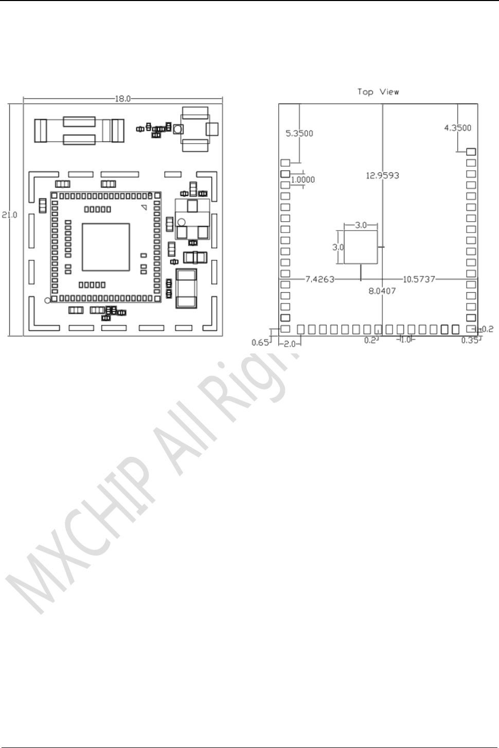
3.9 Mechanical Dimensions
3.9.1 EMW3161 Mechanical Dimensions
Figure 3.1 EMW3161 top view (Metric units)
20
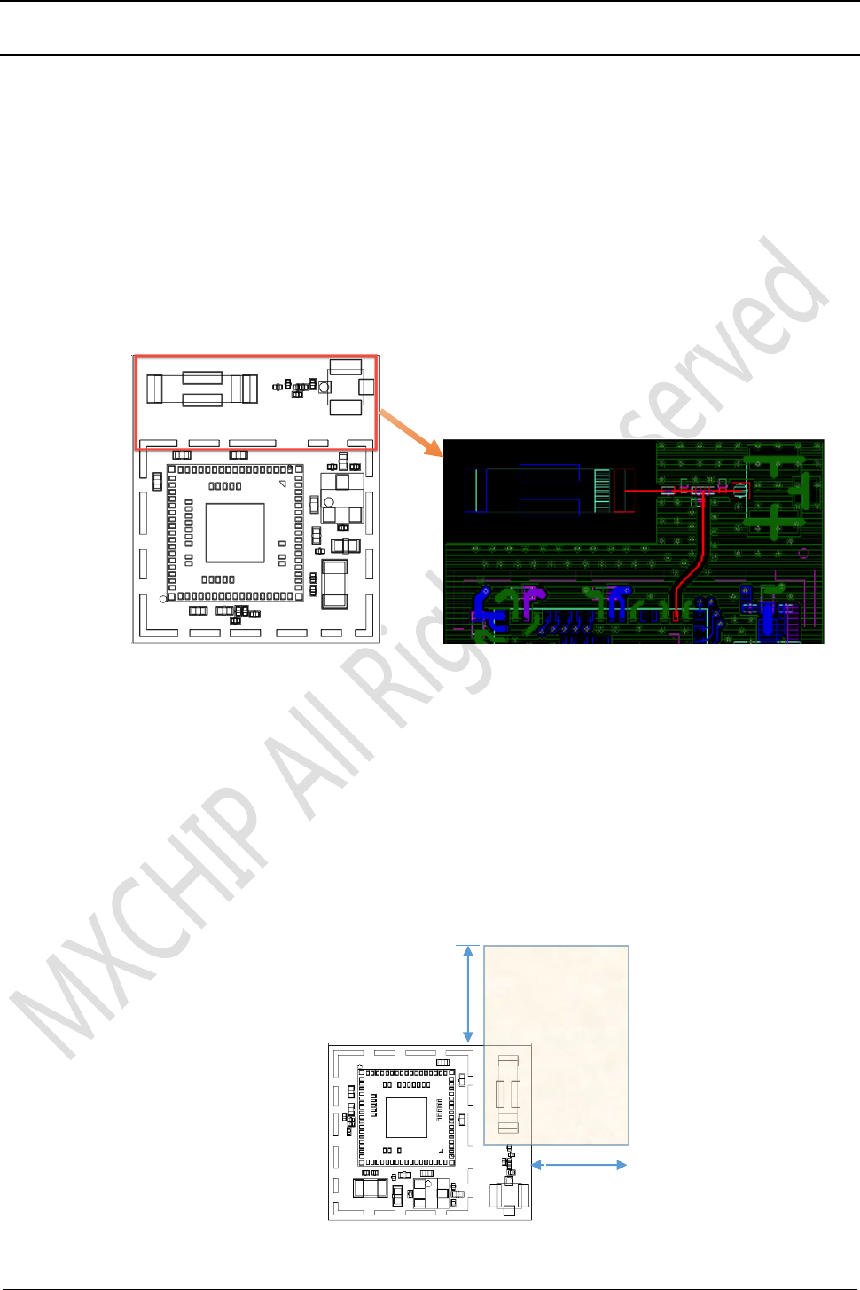
4 Antenna information
There is co-layout design (C35&C32) for antenna connection. Please order your
module carefully. Users can also modify the capacitor position but MXCHIP would not
take any responsibility for this behavior.
EMW3161-E load the capacitor C35 (10pF/0201), it means can use U.F.L RF connector
for external antenna. If want to use on-board chip antenna, just need load the capacitor
from C35 to C32 (EMW3161-C).
In order to get the maximum performance, strongly suggest customer use external
antenna connected with U.F.L RF connector.
4.1 Minimizing radio interference
When integrating the Wi-Fi module with on board PCB printed antenna, make sure
the area around the antenna end the module protrudes at least 15mm from the mother
board PCB and any metal enclosure. If this is not possible use the on board U.FL
connector to route to an external antenna.
The area (6.5mmx17.3mm) under the antenna end of the module should be keep
clear of metallic components, connectors, vias, traces and other materials that can
interfere with the radio signal.
15mm
15mm
21
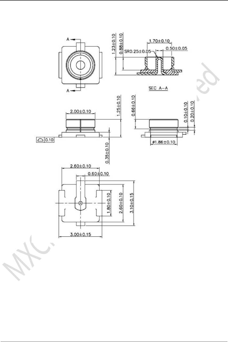
4.2 U.F.L RF Connector
This module use U.F.L type RF connector for external antenna connection.
22
5 Others
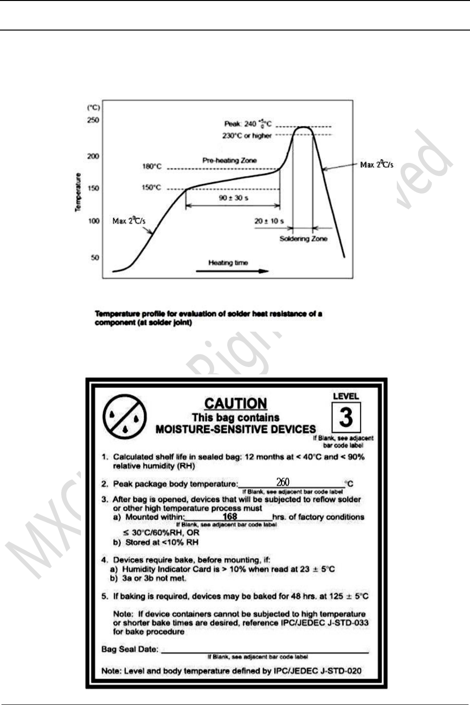
5.1 Recommended Reflow Profile
Reflow times<= 2times (Max.)
5.2 MSL/Storage Condition

23
6 Sales Information
If you need to buy this product, please call MXCHIP during the working hours.
(Monday ~ Friday A.M.9:00~12:00; P.M. 1:00~6:00)
Telephone: +86-21-52655026 / 52655025
Address: Room 811, Tongpu Building, No.1220 Tongpu Road, Shanghai
Post Code: 200333
Email: sales@mxchip.com
7 Technical Support
If you need to get the latest information on this product or our other product
information, you can visit: http://www.mxchip.com/
If you need to get technical support, please call us during the working hours:
ST ARM technical support
+86 (021)52655026-822 Email: support@mxchip.com
Wireless network technical support
+86 (021)58655026-812 Email: support@mxchip.com
Development tools technical support
+86 (021) 52655026-822 Email: support@mxchip.com