Microchip Technology A090665 ATZB-24-B0 2.4GHz B0, 802.15.4/Zigbee OEM- Module User Manual ZigBit 2 4 GHz Wireless Modules ATZB 24 A2 B0
Atmel Norway AS ATZB-24-B0 2.4GHz B0, 802.15.4/Zigbee OEM- Module ZigBit 2 4 GHz Wireless Modules ATZB 24 A2 B0
Contents
- 1. User Manual techn
- 2. User Manual Cert guide
User Manual techn

8226C–MCU Wireless–09/10
ZigBit™ 2.4 GHz Wireless Modules
....................................................................................................................
ATZB-24-A2/B0
Datasheet

ZigBit™ 2.4 GHz Wireless Modules 1-2
8226C–MCU Wireless–09/10

ZigBit™ 2.4 GHz Wireless Modules i
8226C–MCU Wireless–09/10
Table of Contents
Section 1
1.1 Summary............................................................................................................................ 1-1
1.2 Applications........................................................................................................................ 1-1
1.3 Key Features...................................................................................................................... 1-2
1.4 Benefits .............................................................................................................................. 1-2
1.5 Abbreviations and Acronyms ............................................................................................. 1-2
1.6 Related Documents ........................................................................................................... 1-4
Section 2
2.1 Overview ............................................................................................................................ 2-5
Section 3
3.1 Electrical Characteristics.................................................................................................... 3-7
3.1.1 Absolute Maximum Ratings................................................................................. 3-7
3.1.2 Test Conditions.................................................................................................... 3-7
3.1.3 RF Characteristics ............................................................................................... 3-8
3.1.4 ATmega1281V Microcontroller Characteristics ................................................... 3-8
3.1.5 Module Interfaces characteristics ........................................................................ 3-8
3.2 Physical/Environmental Characteristics and Outline ......................................................... 3-9
3.3 Pin Configuration ............................................................................................................. 3-11
3.4 Mounting Information ....................................................................................................... 3-15
3.5 Sample Antenna Reference Designs............................................................................... 3-16
3.5.1 General recommendations ................................................................................ 3-17
3.6 Antenna specifications ..................................................................................................... 3-18
3.6.1 ATZB-24-B0....................................................................................................... 3-18
3.6.2 ATZB-24-A2....................................................................................................... 3-20
Section 4
4.1 UNITED STATES (FCC).................................................................................................. 4-22
4.2 EUROPEAN UNION (ETSI)............................................................................................. 4-23
4.3 Approved Antenna List..................................................................................................... 4-24
Section 5
5.1 Ordering Information ........................................................................................................ 5-25

ZigBit™ 2.4 GHz Wireless Modules 1-1
8226C–MCU Wireless–09/10
Section 1
Introduction
1.1 Summary
ZigBit™ is an ultra-compact, low-power, high-sensitivity 2.4 GHz IEEE 802.15.4/ZigBee® OEM module
based on the innovative Atmel’s mixed-signal hardware platform. It is designed for wireless sensing,
control and data acquisition applications. ZigBit modules eliminate the need for costly and time-consum-
ing RF development, and shortens time to market for a wide range of wireless applications.
Two different versions of 2.4 GHz ZigBit modules are available: ATZB-24-B0 module with balanced RF
port for applications where the benefits of PCB or external antenna can be utilized and ATZB-24-A2
module with dual chip antenna satisfying the needs of applications requiring integrated, small-footprint
antenna design.
1.2 Applications
ZigBit module is compatible with robust IEEE 802.15.4/ZigBee stack that supports a self-healing, self-
organizing mesh network, while optimizing network traffic and minimizing power consumption. Atmel
offers two stack configurations: BitCloud and SerialNet. BitCloud is a ZigBee PRO certified software
development platform supporting reliable, scalable, and secure wireless applications running on Atmel’s
ZigBit modules. SerialNet allows programming of the module via serial AT-command interface.
The applications include, but are not limited to:
•Building automation & monitoring
– Lighting controls
– Wireless smoke and CO detectors
– Structural integrity monitoring
•HVAC monitoring & control
•Inventory management
•Environmental monitoring
•Security
•Water metering
•Industrial monitoring
– Machinery condition and performance monitoring
– Monitoring of plant system parameters such as temperature, pressure, flow, tank level, humidity,
vibration, etc.
•Automated meter reading (AMR)

Introduction
ZigBit™ 2.4 GHz Wireless Modules 1-2
8226C–MCU Wireless–09/10
1.3 Key Features
•Ultra compact size (24 x 13.5 x 2.0 mm for ATZB-24-A2 module and 18.8 x 13.5 x 2.0 mm for ATZB-24-B0
module)
•Innovative (patent-pending) balanced dual chip antenna design with antenna gain of approximately 0 dBi
(for ATZB-24-A2 version)
•High RX sensitivity (-101 dBm)
•Outperforming link budget (104 dB)
•Up to 3 dBm output power
•Very low power consumption:
– < 6 µA in Sleep mode,
– 19 mA in RX mode,
– 18 mA in TX mode
•Ample memory resources (128K bytes of flash memory, 8K bytes RAM, 4K bytes EEPROM)
•Wide range of interfaces (both analog and digital):
– 9 spare GPIO, 2 spare IRQ lines
– 4 ADC lines + 1 line for supply voltage control (up to 9 lines with JTAG disabled)
– UART with CTS/RTS control
–USART
–I
2C
– SPI
–1-Wire
– Up to 30 lines configurable as GPIO
– Capability to write own MAC address into the EEPROM
– Optional antenna reference designs
– IEEE 802.15.4 compliant transceiver
– 2.4 GHz ISM band
– BitCloud embedded software, including serial bootloader and AT command set
1.4 Benefits
•Small physical footprint and low profile for optimum fit in even the smallest of devices
•Best-in-class RF link range
•Extended battery life
•Easy prototyping with 2-layer PCB
•Ample memory for user software application
•Mesh networking capability
•Easy-to-use low cost Evaluation Kit
•Single source of support for HW and SW
•Worldwide license-free operation
1.5 Abbreviations and Acronyms
ADC Analog-to -Digital Converter
API Application Programming Interface
DC Direct Current

Introduction
ZigBit™ 2.4 GHz Wireless Modules 1-3
8226C–MCU Wireless–09/10
DTR Data Terminal Ready
DIP Duap In-line package
EEPROM Electrically Erasable Programmable Read-Only Memory
ESD Electrostatic Discharge
GPIO General Purpose Input/Output
HAL Hardware Abstraction Layer
HVAC Heating, Ventilating and Air Conditioning
HW Hardware
I2C Inter-Integrated Circuit
IEEE Institute of Electrical and Electrionics Engineers
IRQ Interrupt Request
ISM Industrial, Scientific and Medical radio band
JTAG Digital interface for debugging of embedded device, also known as IEEE 1149.1 standard
interface
MAC Medium Access Control layer
MCU Microcontroller Unit. In this document it also means the processor, which is the core of ZigBit
module
NWK Network layer
OEM Original Equipment Manufacturer
OTA Over-The-Air upgrade
PCB Printed Circuit Board
PER Package Error Ratio
PHY Physical layer
RAM Random Access Memory
RF Radio Frequency
RTS/CTS Request to Send/ Clear to Send
RX Receiver
SMA Surface Mount Assembly
SPI Serial Peripheral Interface
SW Software
TTM Time To Market
TX Transmitter
UART Universal Asynchronous Receiver/Transmitter
USART Universal Synchronous/Asynchronous Receiver/Transmitter
USB Universal Serial Bus
ZDK ZigBit Development Kit
ZigBee,
ZigBee PRO Wireless networking standards targeted at low-power applications
802.15.4 The IEEE 802.15.4-2003 standard applicable to low-rate wireless Personal Area Network

Introduction
ZigBit™ 2.4 GHz Wireless Modules 1-4
8226C–MCU Wireless–09/10
1.6 Related Documents
[1] Atmel 8-bit AVR Microcontroller with 64K/128K/256K Bytes In-System Programmable Flash. 2549F
AVR 04/06
[2] Atmel Low-Power Transceiver for ZigBee Applications. AT86RF230 datasheet. doc5131.pdf
[3] IEEE Std 802.15.4-2003 IEEE Standard for Information technology - Part 15.4 Wireless Medium
Access Control (MAC) and Physical Layer (PHY) Specifications for Low-Rate Wireless Personal Area
Networks (LR-WPANs)
[4] ZigBee Specification. ZigBee Document 053474r17, October 19, 2007
[5] BitCloud™ IEEE 802.15.4/ZigBee Software. AVR2050: BitCloud User Guide. Atmels doc8199.pdf
[6] ZigBit™ Development Kit. User's Guide. MeshNetics Doc. S-ZDK-451 - TBD
ZigBit™ 2.4 GHz Wireless Modules 2-5
8226C–MCU Wireless–09/10
Section 2
Zigbit™ Module Overview
2.1 Overview
ZigBit is a low-power, high-sensitivity IEEE 802.15.4/ ZigBee-compliant OEM module. This multi-func-
tional device occupies less than a square inch of space, which is comparable to a typical size of a single
chip. Based on a solid combination of Atmel’s latest MCU Wireless hardware platform [1], the ZigBit
offers superior radio performance, ultra-low power consumption, and exceptional ease of integration.
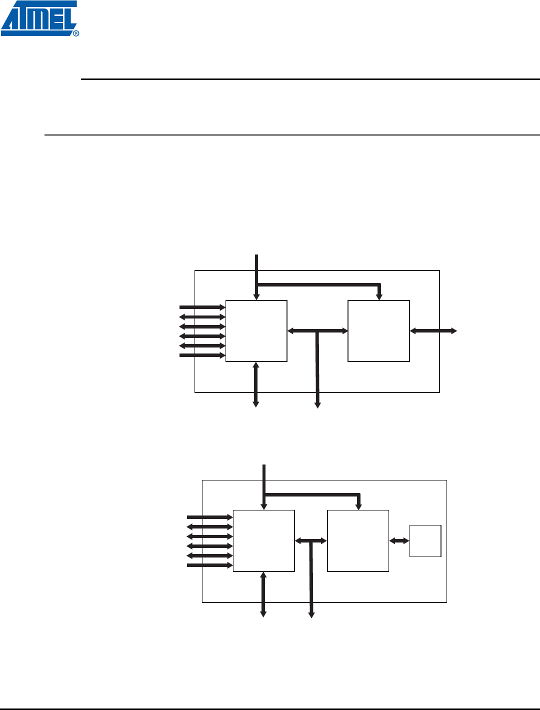
Figure 2-1. ATZB-24-B0 Block Diagram
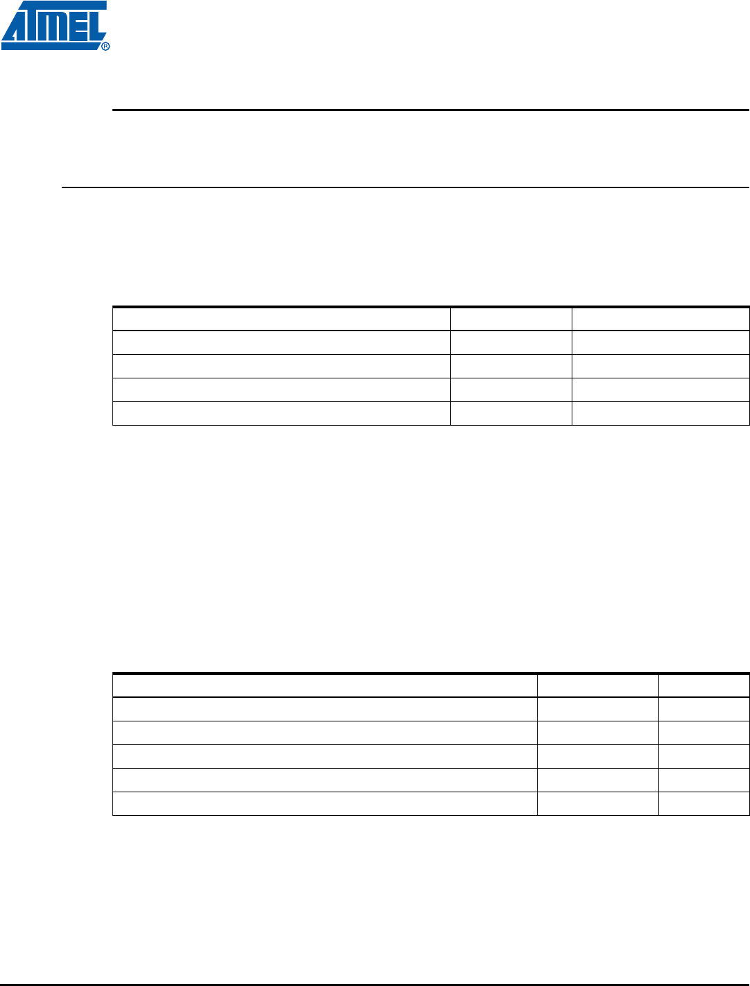
Figure 2-2. ATZB-24-A2 Block Diagram
ATmega1281
AT86RF230
RF
Transceiver
VCC (1.8 - 3.6V)
RF I/O
GPIO SPI Bus
IRQ
UART
USART/SPI
I2C
JTAG
ANALOG
ATmega1281
AT86RF230
RF
Transceiver
VCC (1.8 - 3.6V)
GPIO SPI Bus
IRQ
UART
USART/SPI
I2C
JTAG
ANALOG
Chip
Antenna

Zigbit™ Module Overview
ZigBit™ 2.4 GHz Wireless Modules 2-6
8226C–MCU Wireless–09/10
ZigBit modules comply with the FCC (Part 15), IC and ETSI (CE) rules applicable to the devices radiat-
ing in uncontrolled environment. For details, see “Agency Certifications” on page 4-22.
ZigBit fully satisfies the requirements of the “Directive 2002/95/EC of the European Parliament and the
Council of 27January 2003 on the restriction of the use of certain hazardous substances in electrical and
electronic equipment” (RoHS). Atmel provides fully compliant product in all regions where the directive is
enforced since July 1, 2006.
ZigBit contains Atmel’s ATmega1281V Microcontroller [1] and AT86RF230 RF Transceiver [2]. The mod-
ule features 128 Kbytes flash memory and 8 Kbytes RAM.
The ZigBit already contains a complete RF/MCU-related design with all the necessary passive compo-
nents included. The module can be easily mounted on a simple 2-layer PCB. Compared to a custom
RF/MCU design, a module-based solution offers considerable savings in development time and NRE
cost per unit during the design, prototyping, and mass production phases of product development.
Innovative (patent-pending) dual chip antenna design in ATZB-24-A2 module eliminates the balun and
achieves good performance over 2.4 GHz frequency band.
To jumpstart evaluation and development, Atmel also offers a complete set of evaluation and develop-
ment tools. The ZigBit Development Kit [6] (ATZB-DK-24) comes with everything you need to create
custom applications featuring ZigBit module.
The kit features MeshBean development boards with an easy-to-access extension connector for attach-
ing third party sensors and other peripherals, and a JTAG connector for easy application uploading and
debugging.
The kit also includes reference applications to speed up application development, source code for hard-
ware interface layer and reference drivers for the all the module interfaces, intuitive development
environment from Atmel, and comprehensive set of application notes and product documentation.
ZigBit modules comes bundled with BitCloud, a 2nd generation embedded software stack from Atmel.
BitCloud is fully compliant with ZigBee PRO and ZigBee standards for wireless sensing and control [3],
[4], [5] and it provides an augmented set of APIs which, while maintaining 100% compliance with the
standard, offer extended functionality designed with developer's convenience and ease-of-use in mind.
Depending on end-user design requirements, ZigBit can operate as a self-contained sensor node, where
it would function as a single MCU, or it can be paired with a host processor driving the module over a
serial interface. In the former case, a user application may be used with the BitCloud software allowing
customization of embedded applications through BitCloud’s C API.
In the latter case, the host processor controls data transmission and manages module peripherals via an
extensive set of SerialNet AT commands. Thus, no firmware customization is required for a successful
module design-in. Additionally, third-party sensors can be connected directly to the module, thus
expanding the existing set of peripheral interfaces.
ZigBit™ 2.4 GHz Wireless Modules 3-7
8226C–MCU Wireless–09/10
Section 3
Specifications
3.1 Electrical Characteristics
3.1.1 Absolute Maximum Ratings
Notes: 1. Absolute Maximum Ratings are the values beyond which damage to the device may occur. Under no
circumstances must the absolute maximum ratings given in this table be violated. Stresses beyond
those listed under "Absolute Maximum Ratings" may cause permanent damage to the device.
This is a stress rating only. Functional operation of the device at these or other conditions, beyond those
indicated in the operational sections of this specification, is not implied. Exposure to absolute maximum
rating conditions for extended periods may affect device reliability.
2. Attention! ZigBit is an ESD-sensitive device. Precaution should be taken when handling the device in
order to prevent permanent damage.
3.1.2 Test Conditions
Notes: 1. The parameters are measured under the following conditions:
a) BitCloud Software is running at 4 MHz clock rate, DTR line management is turned off
b) All interfaces are set to the default state (see Pin Assignment Table)
c) Output TX power is 0 dBm
d) JTAG is not connected
2. Supply voltage below 2.7V requires the MCU to be operating at 2 MHz speed
Table 3-1. Absolute Maximum Ratings(1)(2)
Parameters Min Max
Voltage on any pin, except RESET with respect to Ground -0.5V VCC + 0.5V
DC Current per I/O Pin 40 mA
DC Current DVCC and DGND pins 200 mA
Input RF Level +10 dBm
Table 3-2. Test conditions (unless otherwise stated), VCC =3V, T
amb =25°C
Parameters Range Unit
Supply Voltage, VCC
(2) 1.8 to 3.6 V
Current Consumption: RX mode 19 mA
Current Consumption: TX mode(1) 18 mA
Current Consumption: Radio is turned off, MCU is active 50% of the time(1) 14 mA
Current Consumption: Power-save mode(1) 6µA
Specifications
ZigBit™ 2.4 GHz Wireless Modules 3-8
8226C–MCU Wireless–09/10
Current consumption actually depends on multiple factors, including but not limited to, the board design
and materials, BitCloud settings, network activity, EEPROM read/write operations. It also depends on
MCU load and/or peripherals used by an application.
3.1.3 RF Characteristics
3.1.4 ATmega1281V Microcontroller Characteristics
3.1.5 Module Interfaces characteristics
Table 3-3. RF Characteristics
Parameters Condition Range Unit
Frequency Band 2.4000 to 2.4835 GHz
Numbers of Channels 16
Channel Spacing 5 MHz
Transmitter Output Power Adjusted in 16 steps -17 to +3 dBm
Receiver Sensitivity PER = 1%
On-Air Data Rate 250 kbps
TX Output/ RX Input Nominal Impedance For balanced output 100 Ω
Table 3-4. ATmega1281V Characteristics
Parameters Condition Range Unit
On-chip Flash Memory size 128K bytes
On-chip RAM size 8K bytes
On-chip EEPROM size 4K bytes
Operation Frequency 4 MHz
Table 3-5. Module Interfaces characteristics
Parameters Condition Range Unit
UART Maximum Baud Rate 38.4 kbps
ADC Resolution/ Conversion Time In single conversion
mode 10/200 Bits/µs
ADC Input Resistance >1 MΩ
ADC Reference Voltage (VREF) 1.0 to VCC -3 V
ADC Input Voltage 0 - VREF V
I2C Maximum Clock 222 kHz
GPIO Output Voltage (High/Low) -10/ 5 mA 2.3/ 0.5 V
Real Time Oscillator Frequency 32.768 kHz
Specifications
ZigBit™ 2.4 GHz Wireless Modules 3-9
8226C–MCU Wireless–09/10
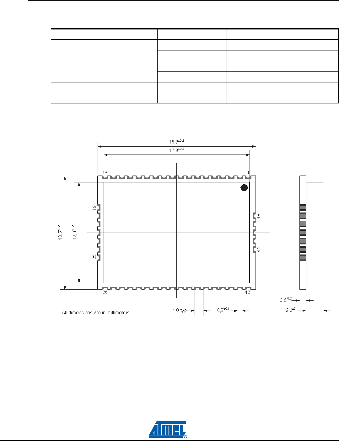
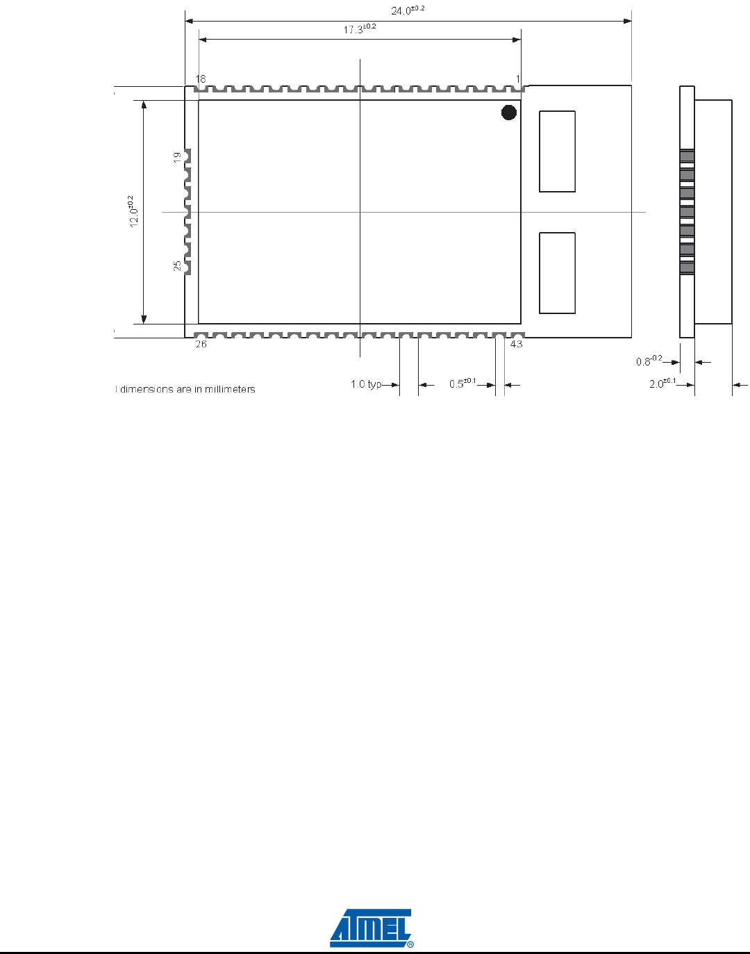
3.2 Physical/Environmental Characteristics and Outline
Note: 1. Minor degration of clock stability may occur.
Figure 3-1. ATZB-24-B0 Mechanical drawing
Parameters Value Comments
Size 18.8 x 13.5 x 2.0 mm ATZB-24-B0
24.0 x 13.5 x 2.0 mm ATZB-24-A2
Weight 1.3g ATZB-24-B0
1.5g ATZB-24-A2
Operating Temperature Range -20°C to +70°C-40°C to +85°C operational(1)
Operating Relative Humidity Range no more than 80%
Specifications
ZigBit™ 2.4 GHz Wireless Modules 3-10
8226C–MCU Wireless–09/10
Figure 3-2. ATZB-24-A2 Mechanical drawing
Specifications
ZigBit™ 2.4 GHz Wireless Modules 3-11
8226C–MCU Wireless–09/10
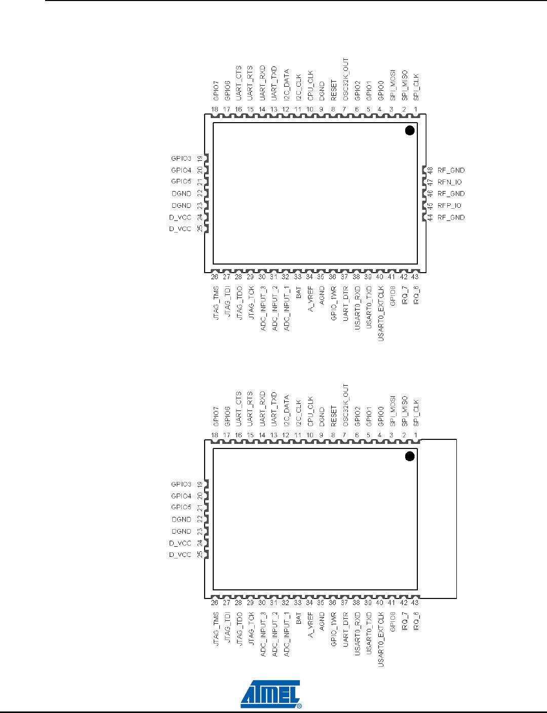
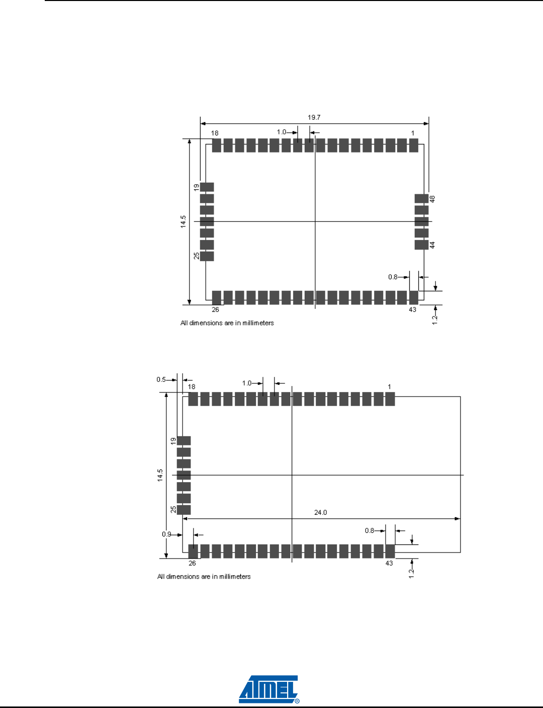
3.3 Pin Configuration
Figure 3-3. ATZB-24-B0 Pinout
Figure 3-4. ATZB-24-A2 Pinout

Specifications
ZigBit™ 2.4 GHz Wireless Modules 3-12
8226C–MCU Wireless–09/10
Table 3-6. Pin descriptions
Connector
Pin Pin Name Description I/O
Default
State after
Power on
1 SPI_CLK Reserved for stack operation(4) O
2 SPI_MISO Reserved for stack operation(4) I/O
3 SPI_MOSI Reserved for stack operation(4) I/O
4 GPIO0 General Purpose digital Input/Output 0(2)(3)(4)(7) I/O tri-state
5 GPIO1 General Purpose digital Input/Output 1(2)(3)(4)(7) I/O tri-state
6 GPIO2 General Purpose digital Input/Output 2(2)(3)(4)(7) I/O tri-state
7 OSC32K_OUT 32.768 kHz clock output(4)(5) O
8 RESET Reset input (active low)(4)
9,22,23 DGND Digital Ground
10 CPU_CLK
RF clock output. When module is in active state, 4
MHz signal is present on this line. While module is
in the sleeping state, clock generation is also
stopped(4).
O
11 I2C_CLK I2C Serial clock output(2)(3)(4)(7) O tri-state
12 I2C_DATA I2C Serial data input/output(2)(3)(4)(7) I/O tri-state
13 UART_TXD UART receive input(1)(2)(3)(4)(7) I tri-state
14 UART_RXD UART transmit output(1)(2)(3)(4)(7) O tri-state
15 UART_RTS RTS input (Request to send) for UART hardware
flow control. Active low(2)(3)(4)(7) I tri-state
16 UART_CTS CTS output (Clear to send) for UART hardware
flow control. Active low(2)(3)(4)(7)(8) O tri-state
17 GPIO6 General Purpose digital Input/Output 6(2)(3)(4)(7) I/O tri-state
18 GPIO7 General Purpose digital Input/Output 7(2)(3)(4)(7) I/O tri-state
19 GPIO3 General Purpose digital Input/Output 3(2)(3)(4)(7) I/O tri-state
20 GPIO4 General Purpose digital Input/Output 4(2)(3)(4)(7) I/O tri-state
21 GPIO5 General Purpose digital Input/Output 5(2)(3)(4)(7) I/O tri-state
24,25 D_VCC Digital Supply Voltage (VCC)(9)
26 JTAG_TMS JTAG Test Mode Select(2)(3)(4)(6) I
27 JTAG_TDI JTAG Test Data Input(2)(3)(4)(6) I
28 JTAG_TDO JTAG Test Data Output(2)(3)(4)(6) O
29 JTAG_TCK JTAG Test Clock(2)(3)(4)(6) I
30 ADC_INPUT_3 ADC Input Channel 3(2)(3)(7) I tri-state
31 ADC_INPUT_2 ADC Input Channel 2(2)(3)(7) I tri-state
32 ADC_INPUT_1 ADC Input Channel 1(2)(3)(7) I tri-state
33 BAT ADC Input Channel 0, used for battery level
measurement. This pin equals VCC/3.(2)(3)(7) I tri-state
34 A_VREF Input/Output reference voltage for ADC I/O tri-state
Specifications
ZigBit™ 2.4 GHz Wireless Modules 3-13
8226C–MCU Wireless–09/10
Notes: 1. The UART_TXD pin is intended for input (i.e. its designation as "TXD" implies some complex system
containing ZigBit as its RF terminal unit), while UART_RXD pin, vice versa, is for output.
2. Most of pins can be configured for general purpose I/O or for some alternate functions as described in
details in the ATmega1281V Datasheet [1].
3. GPIO pins can be programmed either for output, or for input with/without pull-up resistors. Output pin
drivers are strong enough to drive LED displays directly (refer to figures on pages 387-388, [1]).
4. All digital pins are provided with protection diodes to D_VCC and DGND
5. It is strongly recommended to avoid assigning an alternate function for OSC32K_OUT pin because it is
used by BitCloud. However, this signal can be used if another peripheral or host processor requires
32.768 kHz clock, otherwise this pin can be disconnected.
6. Normally, JTAG_TMS, JTAG_TDI, JTAG_TDO, JTAG_TCK pins are used for on-chip debugging and
flash burning. They can be used for A/D conversion if JTAGEN fuse is disabled.
7. The following pins can be configured with the BitCloud software to be general-purpose I/O lines:
GPIO0, GPIO1, GPIO2, GPIO3, GPIO4, GPIO5, GPIO6, GPIO7, GPIO8, GPIO_1WR, I2C_CLK,
I2C_DATA, UART_TXD, UART_RXD, UART_RTS, UART_CTS, ADC_INPUT_3, ADC_INPUT_2,
ADC_INPUT_1, BAT, UART_DTR, USART0_RXD, USART0_TXD, USART0_EXTCLK, IRQ_7, IRQ_6.
Additionally, four JTAG lines can be programmed with software as GPIO as well, but this requires
changing the fuse bits and will disable JTAG debugging.
8. With BitCloud, CTS pin can be configured to indicate sleep/active condition of the module thus provid-
ing mechanism for power management of host processor. If this function is necessary, connection of
this pin to external pull-down resistor is recommended to prevent the undesirable transients during
module reset process.
35 AGND Analog ground
36 GPIO_1WR 1-wire interface(2)(3)(4)(7) I/O
37 UART_DTR DTR input (Data Terminal Ready) for UART.
Active low(2)(3)(4)(7) I tri-state
38 USART0_RXD USART/SPI Receive pin(2)(3)(4)(7) I tri-state
39 USART0_TXD USART /SPI Transmit pin(2)(3)(4)(7) O tri-state
40 USART0_EXTCLK USART/SPI External Clock(2)(3)(4)(7)(11) I/O tri-state
41 GPIO8 General Purpose Digital Input/Output I/O tri-state
42 IRQ_7 Digital Input Interrupt request 7(2)(3)(4)(7) I tri-state
43 IRQ_6 Digital Input Interrupt request 6(2)(3)(4)(7) I tri-state
44,46,48 RF GND RF Analog Ground(2)(3)(4)(7)
45 RFP_IO Differential RF Input/Output(10) I/O
47 RFN_IO Differential RF Input/Output(10) I/O
Table 3-6. Pin descriptions
Connector
Pin Pin Name Description I/O
Default
State after
Power on
Specifications
ZigBit™ 2.4 GHz Wireless Modules 3-14
8226C–MCU Wireless–09/10
9. Using ferrite bead and 1 µF capacitor located closely to the power supply pin is recommended, as
shown below.
10. Pins 44 through 48 are not designed for the ATZB-24-A2 module. Note these pins are used in
ATZB-24-B0, see them in antenna schematics below.
11. In SPI mode, USART0_EXTCLK is output. In USART mode, this pin can be configured as either input
or output pin.
For ATZB-24-B0 combined with PCB
Antenna
For ATZB-24-B0 combined with External
Antenna
Specifications
ZigBit™ 2.4 GHz Wireless Modules 3-15
8226C–MCU Wireless–09/10
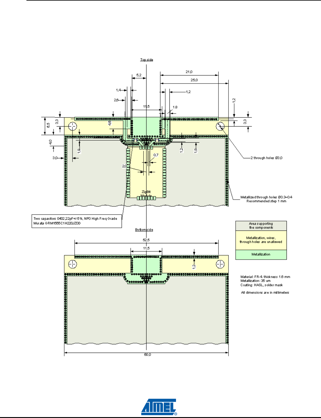
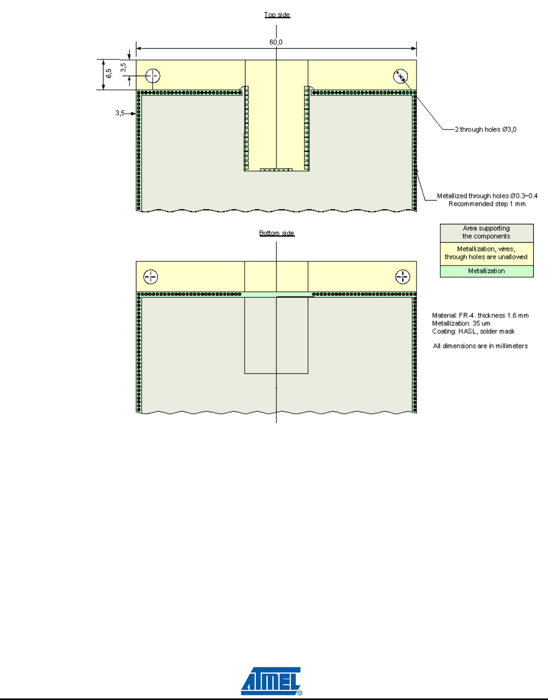
3.4 Mounting Information
The below diagrams show the PCB layout recommended for ZigBit module. Neither via-holes nor wires
are allowed on the PCB upper layer in area occupied by the module. As a critical requirement, RF_GND
pins should be grounded via several holes to be located right next to the pins thus minimizing inductance
and preventing both mismatch and losses.
Figure 3-5. ATZB-24-B0 PCB Recommended Layout, Top View
Figure 3-6. ATZB-24-A2 PCB Recommended Layout, Top View
Specifications
ZigBit™ 2.4 GHz Wireless Modules 3-16
8226C–MCU Wireless–09/10
3.5 Sample Antenna Reference Designs
This section presents PCB designs which combine ZigBit with different antennas: PCB onboard
antenna, external antenna and dual chip antenna. These antenna reference designs are recommended
for successful design-in.
Figure 3-7. PCB Layout: Symmetric Dipole Antenna recommended for ATZB-24-B0
The symmetric dipole antenna above has been tuned for the particular design. The 'cut-and-paste'
approach would not guarantee optimal performance because of multiple factors affecting proper antenna

Specifications
ZigBit™ 2.4 GHz Wireless Modules 3-17
8226C–MCU Wireless–09/10
match, hence, affecting the pattern. The particular factors are the board material and thickness, shields,
the material used for enclosure, the board neighborhood, and other components adjacent to antenna.
3.5.1 General recommendations
Metal enclosure should not be used. Using low profile enclosure might also affect antenna tuning.
Placing high profile components next to antenna should be avoided.
Having holes punched around the periphery of the board eliminates parasitic radiation from the board
edges also distorting antenna pattern.
ZigBit module should not be placed next to consumer electronics which might interfere with ZigBit's RF
frequency band.
Specifications
ZigBit™ 2.4 GHz Wireless Modules 3-18
8226C–MCU Wireless–09/10
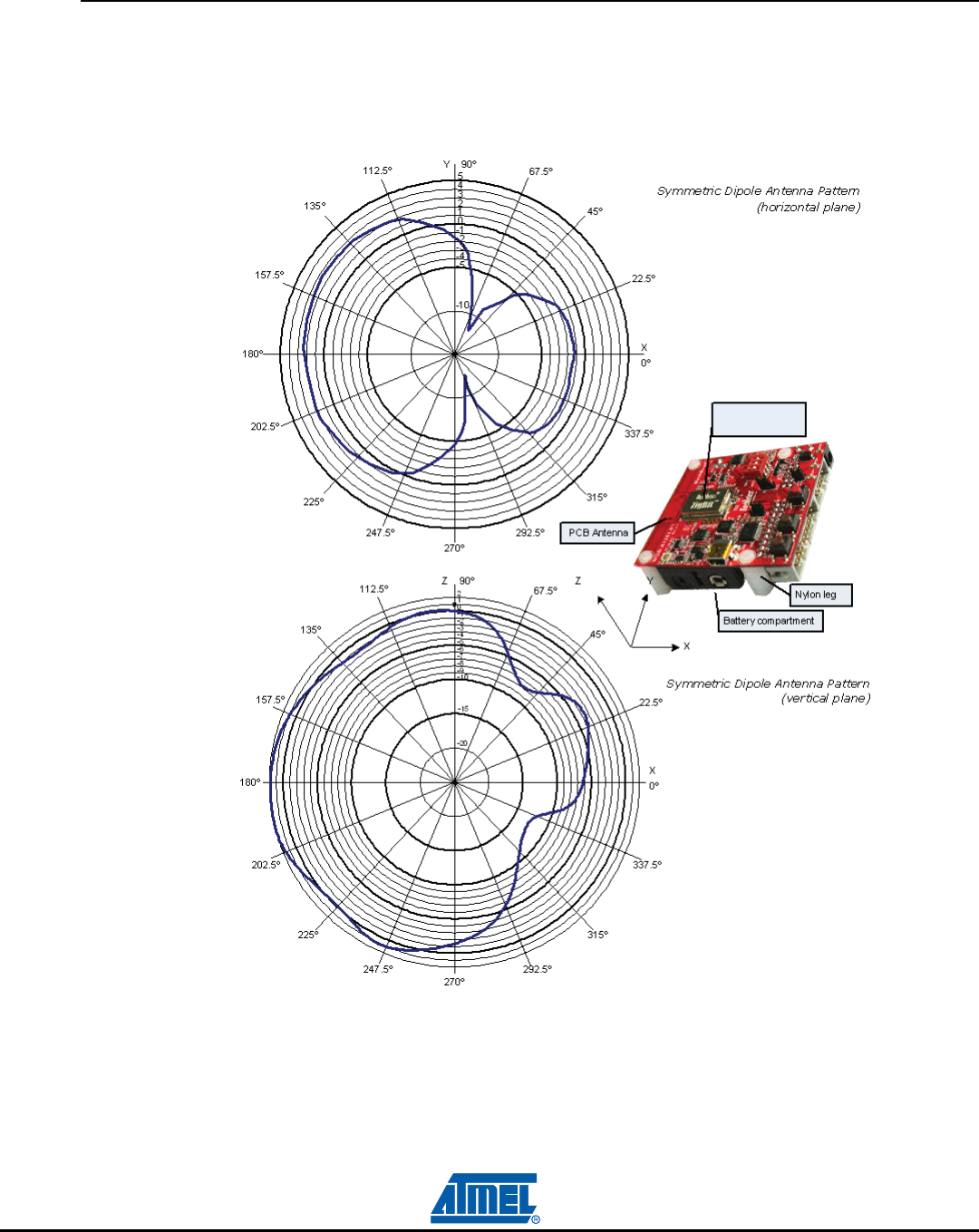
3.6 Antenna specifications
3.6.1 ATZB-24-B0
Figure 3-8. Symmetric Dipole Antenna Pattern (horizontal and vertical plane) for ATZB-24-B0
ATZB-24-B0
ATZB-24-B0:
ATZB-24-B0:
Specifications
ZigBit™ 2.4 GHz Wireless Modules 3-19
8226C–MCU Wireless–09/10
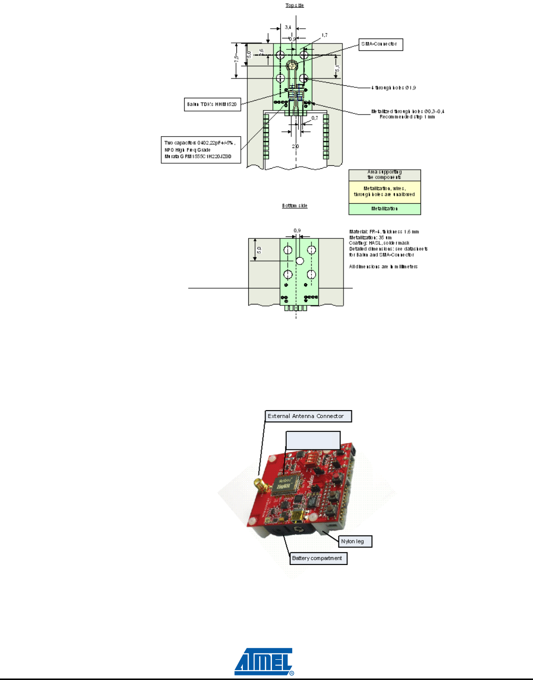
Figure 3-9. PCB Layout with 50 Ohm External Antenna recommended for ATZB-24-B0
In case the external unbalanced 50 Ohm antenna is required, it can be easily interfaced to ATZB-24-B0
module by using 2:1 balun as shown above. The reference design in Figure 3-10 demonstrates how to
use SMA connector.
Figure 3-10. SMA connectors
ATZB-24-B0
Specifications
ZigBit™ 2.4 GHz Wireless Modules 3-20
8226C–MCU Wireless–09/10
3.6.2 ATZB-24-A2
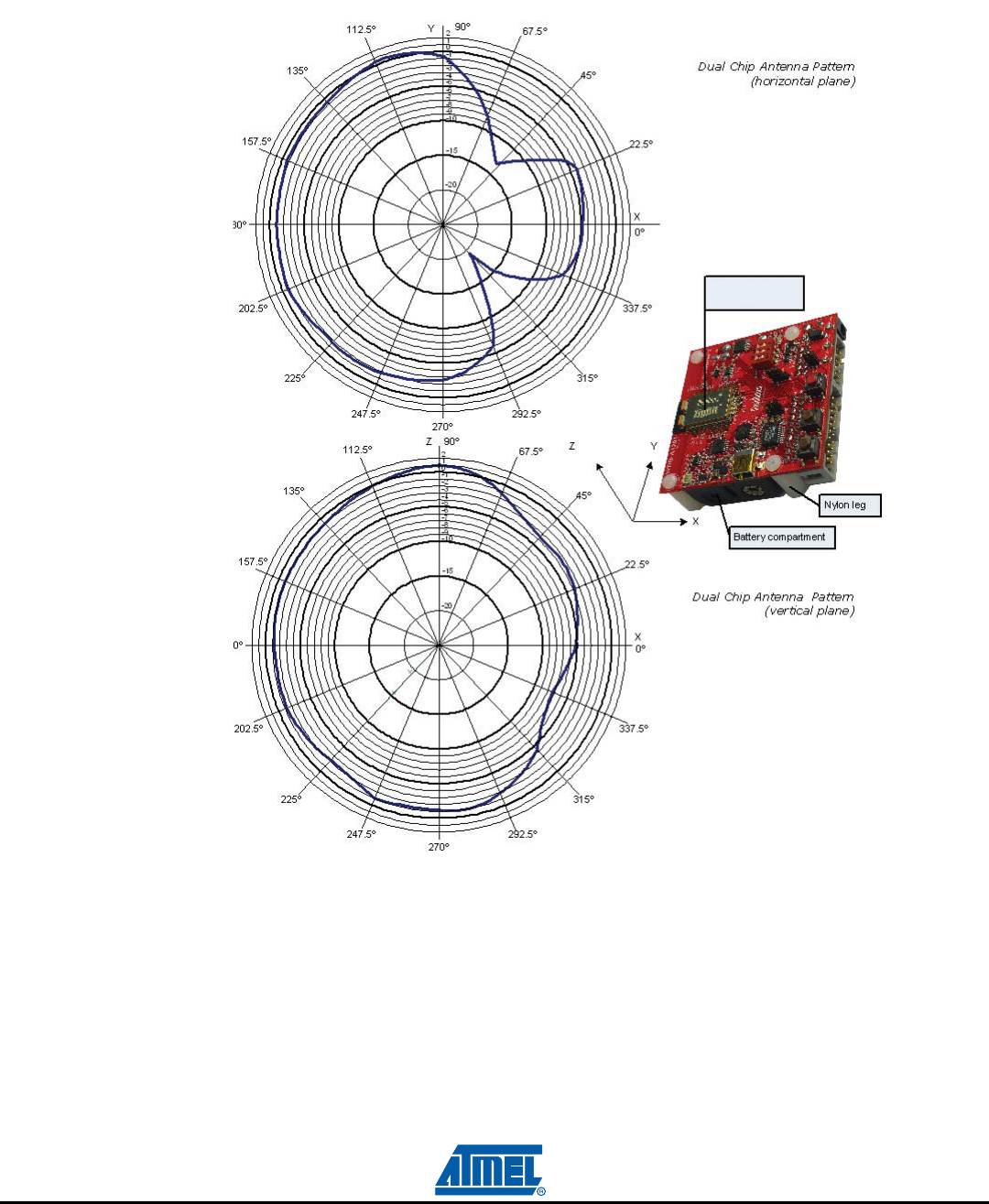
Figure 3-11. Symmetric Dipole Antenna Pattern (horizontal and vertical plane) for ATZB-24-A2
Note: The antenna patterns presented above were observed using PCB enhanced with legs made of original
nylon.
ATZB-24-A2
ATZB-24-A2:
ATZB-24-A2:
Specifications
ZigBit™ 2.4 GHz Wireless Modules 3-21
8226C–MCU Wireless–09/10
Figure 3-12. PCB Layout with Dual Chip Antenna Module recommended for ATZB-24-A2
Normally, chip antennas are more tolerant of the board or enclosure materials in ZigBit's neighborhood
as well. However, general recommendations given above for the PCB antenna design still apply.
The board design should prevent propagation of microwave field inside the board material. Electromag-
netic waves of high frequency may penetrate the board thus making the edges of the board radiate,
which may distort the antenna pattern. To eliminate this effect, metalized and grounded holes must be
placed around the board's edges as shown.
Since the design of dual chip antenna is intended for installation on FR-4 board 1.6 mm thick, the
antenna performance may only be guaranteed for the particular board type and thickness.
ZigBit™ 2.4 GHz Wireless Modules 4-22
8226C–MCU Wireless–09/10
Section 4
Agency Certifications
4.1 UNITED STATES (FCC)
This equipment complies with Part 15 of the FCC rules and regulations.
To fulfill FCC Certification requirements, an OEM manufacturer must comply with the following
regulations:
1. The modular transmitter must be labelled with its own FCC ID number, and, if the FCC ID is not visi-
ble when the module is installed inside another device, then the outside of the device into which the
module is installed must also display a label referring to the enclosed module. This exterior label can
use wording such as the following:
Example of label required for OEM product containing ATZB-24-A2 module
Example of label required for OEM product containing ATZB-24-B0 module
Any similar wording that expresses the same meaning may be used.
2. To be used with the ATZB-24-B0 module, the external antennas have been tested and approved
which are specified in here below. The ATZB-24-B0 Module may be integrated with other custom
design antennas which OEM installer must authorize following the FCC 15.21 requirements.
WARNING: The Original Equipment Manufacturer (OEM) must ensure that the OEM modular transmitter
must be labeled with its own FCC ID number. This includes a clearly visible label on the outside of the
final product enclosure that displays the contents shown below. If the FCC ID is not visible when the
equipment is installed inside another device, then the outside of the device into which the equipment is
installed must also display a label referring to the enclosed equipment.
IMPORTANT: This equipment complies with Part 15 of the FCC Rules. Operation is subject to the follow-
ing two conditions: (1) this device may not cause harmful interference, and (2) this device must accept
any interference received, including interference that may cause undesired operation (FCC 15.19).
The internal / external antenna(s) used for this mobile transmitter must provide a separation distance of
at least 20 cm from all persons and must not be co-located or operating in conjunction with any other
antenna or transmitter.
Contains FCC ID: VW4A090664
The enclosed device complies with Part 15 of the FCC Rules. Operation is subject to the following two conditions:
(i.) this device may not cause harmful interference and (ii.) this device must accept any interference received,
including interference that may cause undesired operation.
Contains FCC ID: VW4A090665
The enclosed device complies with Part 15 of the FCC Rules. Operation is subject to the following two conditions:
(i.) this device may not cause harmful interference and (ii.) this device must accept any interference received,
including interference that may cause undesired operation.

Agency Certifications
ZigBit™ 2.4 GHz Wireless Modules 4-23
8226C–MCU Wireless–09/10
Installers must be provided with antenna installation instructions and transmitter operating conditions for
satisfying RF exposure compliance. This device is approved as a mobile device with respect to RF expo-
sure compliance, and may only be marketed to OEM installers. Use in portable exposure conditions
(FCC 2.1093) requires separate equipment authorization.
IMPORTANT: Modifications not expressly approved by this company could void the user's authority to
operate this equipment (FCC section 15.21).
IMPORTANT: This equipment has been tested and found to comply with the limits for a Class A digital
device, pursuant to Part 15 of the FCC Rules. These limits are designed to provide reasonable protec-
tion against harmful interference when the equipment is operated in a commercial environment. This
equipment generates, uses, and can radiate radio frequency energy and, if not installed and used in
accordance with the instruction manual, may cause harmful interference to radio communications. Oper-
ation of this equipment in a residential area is likely to cause harmful interference in which case the user
will be required to correct the interference at his own expense (FCC section 15.105).
4.2 EUROPEAN UNION (ETSI)
The ATZB-24-A2 and ATZB-24-B0 Modules has been certified for use in European Union countries.
If the ATZB-24-A2 and ATZB-24-B0 Modules are incorporated into a product, the manufacturer must
ensure compliance of the final product to the European harmonized EMC and low-voltage/safety stan-
dards. A Declaration of Conformity must be issued for each of these standards and kept on file as
described in Annex II of the R&TTE Directive.
Furthermore, the manufacturer must maintain a copy of the ATZB-24-A2 and ATZB-24-B0 Modules doc-
umentation and ensure the final product does not exceed the specified power ratings, antenna
specifications, and/or installation requirements as specified in the user manual. If any of these specifica-
tions are exceeded in the final product, a submission must be made to a notified body for compliance
testing to all required standards.
IMPORTANT: The 'CE' marking must be affixed to a visible location on the OEM product. The CE mark
shall consist of the initials "CE" taking the following form:
If the CE marking is reduced or enlarged, the proportions given in the above graduated drawing must
be respected.
The CE marking must have a height of at least 5mm except where this is not possible on account of
the nature of the apparatus.
The CE marking must be affixed visibly, legibly, and indelibly.
More detailed information about CE marking requirements you can find at "DIRECTIVE 1999/5/EC OF
THE EUROPEAN PARLIAMENT AND OF THE COUNCIL" on 9 March 1999 at section 12.
Certification Approved Antennas list is presented in below.
Agency Certifications
ZigBit™ 2.4 GHz Wireless Modules 4-24
8226C–MCU Wireless–09/10
4.3 Approved Antenna List
ATZB-24-A2 Module works with integrated dual chip antenna. The design of the antenna is fully compli-
ant with all the aforementioned regulation.
ATZB-24-B0 Module has been tested and approved for use with the antennas listed in the table below.
ATZB-24-0B Module may be integrated with other custom design antennas which OEM installer must
authorize with respective regulatory agencies.
Table 4-1. Approved Antenna specifications
Part Number Manufacture and description Gain [dBi] Minimum separation [cm]
2010B48-01
Antenova Titanis, swivel antenna (1/4 wave
antenna) with SMA connector, frequency range 2.4
- 2.5 GHz
2.2 20
17010.10 WiMo, swivel antenna (1/2 wave antenna) with SMA
connector, frequency range 2.35 - 2.5 GHz 2.1 20
ZigBit™ 2.4 GHz Wireless Modules 5-25
8226C–MCU Wireless–09/10
Section 5
Ordering Information
5.1 Ordering Information
Note: Tape&Reel quantity: 200
Part Number Description
ATZB-24-B0R 2.4 GHz IEEE802.15.4/ZigBee OEM Module w/ Balanced RF Port
ATZB-24-A2R 2.4 GHz IEEE802.15.4/ZigBee OEM Module with dual chip antenna

8226C–MCU Wireless–09/10
© 2010 Atmel Corporation. All rights reserved. Atmel®, Atmel logo and combinations thereof, AVR®, AVR® logo and others are registered trade-
marks or trademarks of Atmel Corporation or its subsidiaries. Other terms and product names may be trademarks of others.
Headquarters International
Atmel Corporation
2325 Orchard Parkway
San Jose, CA 95131
USA
Tel: 1(408) 441-0311
Fax: 1(408) 487-2600
Atmel Asia
Unit 1-5 & 16, 19/F
BEA Tower, Millennium City 5
418 Kwun Tong Road
Kwun Tong, Kowloon
Hong Kong
Tel: (852) 2245-6100
Fax: (852) 2722-1369
Atmel Europe
Le Krebs
8, Rue Jean-Pierre Timbaud
BP 309
78054 Saint-Quentin-en-
Yvelines Cedex
France
Tel: (33) 1-30-60-70-00
Fax: (33) 1-30-60-71-11
Atmel Japan
9F, Tonetsu Shinkawa Bldg.
1-24-8 Shinkawa
Chuo-ku, Tokyo 104-0033
Japan
Tel: (81) 3-3523-3551
Fax: (81) 3-3523-7581
Product Contact
Web Site
www.atmel.com
Technical Support
avr@atmel.com
Sales Contact
www.atmel.com/contacts
Literature Requests
www.atmel.com/literature
Disclaimer: The information in this document is provided in connection with Atmel products. No license, express or implied, by estoppel or otherwise, to any
intellectual property right is granted by this document or in connection with the sale of Atmel products. EXCEPT AS SET FORTH IN ATMEL’S TERMS AND CONDI-
TIONS OF SALE LOCATED ON ATMEL’S WEB SITE, ATMEL ASSUMES NO LIABILITY WHATSOEVER AND DISCLAIMS ANY EXPRESS, IMPLIED OR STATUTORY
WARRANTY RELATING TO ITS PRODUCTS INCLUDING, BUT NOT LIMITED TO, THE IMPLIED WARRANTY OF MERCHANTABILITY, FITNESS FOR A PARTICULAR
PURPOSE, OR NON-INFRINGEMENT. IN NO EVENT SHALL ATMEL BE LIABLE FOR ANY DIRECT, INDIRECT, CONSEQUENTIAL, PUNITIVE, SPECIAL OR INCIDEN-
TAL DAMAGES (INCLUDING, WITHOUT LIMITATION, DAMAGES FOR LOSS OF PROFITS, BUSINESS INTERRUPTION, OR LOSS OF INFORMATION) ARISING OUT OF
THE USE OR INABILITY TO USE THIS DOCUMENT, EVEN IF ATMEL HAS BEEN ADVISED OF THE POSSIBILITY OF SUCH DAMAGES. Atmel makes no
representations or warranties with respect to the accuracy or completeness of the contents of this document and reserves the right to make changes to specifications
and product descriptions at any time without notice. Atmel does not make any commitment to update the information contained herein. Unless specifically provided
otherwise, Atmel products are not suitable for, and shall not be used in, automotive applications. Atmel’s products are not intended, authorized, or warranted for use
as components in applications intended to support or sustain life.