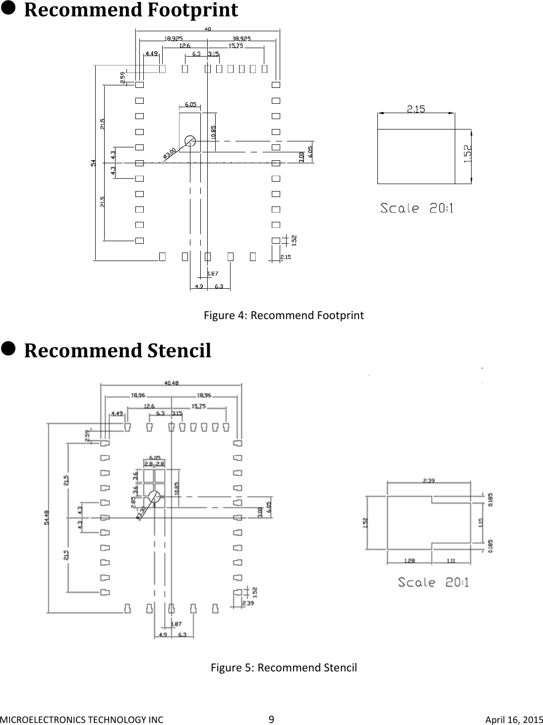
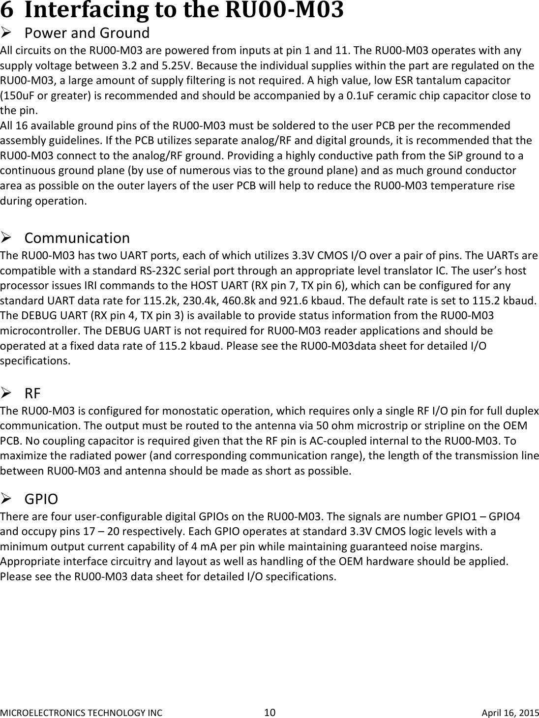
Microelectronics Technology RU00-M03 RFID HP-SIP Module User Manual

Microelectronics Technology Inc RFID HP-SIP Module

User Manual.pdf

               RFID High Power SiP RU00-M03-X001 / X011  Quick Guide Version 1.0.0               MTI Group Proprietary Information  Any  unauthorized  use,  duplication,  reproduction,  reverse  engineering, decompilation,  or  disclosure  of  this  document  may  be  considered  as infringement of MTI Group’s intellectual property rights, the infringer may be accused and liable applicable legal penalties.  Copyright, Microelectronics Technology Inc.. All rights reserved.
MICROELECTRONICS TECHNOLOGY INC  2  April 16, 2015 Table of Contents  1 Introduction............................................................................................................................................................... 3 2 Regulatory Statement ............................................................................................................................................... 4  Federal Communication Commission Interference Statement ................................................................ 4 3 Block Diagram ........................................................................................................................................................... 5 4 Pin Configurations and Descriptions ....................................................................................................................... 6 5 Package Descriptions ................................................................................................................................................ 8  Package Mechanical Outline ..................................................................................................................... 8  Recommend Footprint .............................................................................................................................. 9  Recommend Stencil .................................................................................................................................. 9 8 Revision history ...................................................................................................................................................... 12  Figures  Figure 1: System Block Diagram ..................................................................................................................................... 5 Figure 2: Pin Configurations ........................................................................................................................................... 6 Figure 3: Package Mechanical Outline ........................................................................................................................... 8 Figure 4: Recommend Footprint .................................................................................................................................... 9 Figure 5: Recommend Stencil ........................................................................................................................................ 9  Tables  Table 1: Band configurations ......................................................................................................................................... 3 Table 2: Pin Descriptions ............................................................................................................................................... 7 Table 3: Revision history ............................................................................................................................................ 12
MICROELECTRONICS TECHNOLOGY INC  3  April 16, 2015 1 Introduction The RU00-M03 is a System in Package (SiP) that comprises a completely in integrated solution for EPC Gen 2 / ISO18000-63 (formerly 18000-6C) application.  The SiP was developed to make embedding UHF RFID reader capability easy. The RU00-M03 builds on market-leading Indy reader chip technology and integrates all of the necessary components into a tiny package. It requires very few external components. The RU00-M03 comes in a surface mount package designed to work as a SMT (surface mount technology) component in a standard PCB manufacturing process.  This  document  provides  instructions  to  the  end-user  to  ensure  optimal  performance  in  their  OEM hardware. Details on the use of the RU00-M03 Development Kit are also included to provide an example of appropriate application.  Model Number  Supported Regions  Operating Frequency RU00-M03-X001  US  902.75MHz~927.25MHz EU  866.3MHz~867.5MHz RU00-M03-X011  CN  920.625MHz~924.375MHz JP  916.8MHz~920.4MHz Table 1: Band configurations Regions configuration in different end-use products is limited by an original equipment manufacturer (OEM)
MICROELECTRONICS TECHNOLOGY INC  4  April 16, 2015 2 Regulatory Statement  Federal Communication Commission Interference Statement  This device complies with Part 15 of the FCC Rules. Operation is subject to the following two conditions: (1) This device may not cause harmful interference, and (2) this device must accept any interference received, including interference that may cause undesired operation.  This equipment has been tested and found to comply with the limits for a Class B digital device, pursuant to Part 15 of the FCC Rules.  These limits are designed to provide reasonable protection against harmful interference in a residential installation. This equipment generates, uses and can radiate radio frequency energy and, if not installed and used in accordance with the instructions, may cause harmful interference to radio communications.  However, there is no guarantee that interference will not occur in a particular installation.  If this equipment does cause harmful interference to radio or television reception, which can be determined by turning the equipment off and on, the user is encouraged to try to correct the interference by one of the following measures:  -Reorient or relocate the receiving antenna. -Increase the separation between the equipment and receiver. -Connect the equipment into an outlet on a circuit different from that to which the receiver is connected. -Consult the dealer or an experienced radio/TV technician for help.  FCC Caution: Any changes or modifications not expressly approved by the party responsible for compliance could void the user's authority to operate this equipment.  Radiation Exposure Statement: This equipment complies with FCC radiation exposure limits set forth for an uncontrolled environment. This equipment should be installed and operated with minimum distance 21cm between the radiator & your body.
MICROELECTRONICS TECHNOLOGY INC  5  April 16, 2015 3 Block Diagram  An example of a RU00-M03 system-level block diagram for an embedded application is shown in Figure 1.  Required connections:   VDC and GND are required to power the RU00-M03.   RF pin must be connected to the OEM antenna.   UART1 provides host communications to control the operation of the RU00-M03.   ENABLE pin resets the RU00-M03 when set low.   Recommended connections:   UART2 provides debug information.   HEALTH indicates successful boot of the RU00-M03. Connection to an LED provides a visual indication of whether or not an error condition exists.   STATUS provides an indication when the RU00-M03 is inventorying tags. Connection to an LED provides a visual indicator of the tag activity.   Optional connections:   GPIO allow the user to provide general-purpose user-controlled digital I/O   WAKEUP is a digital input which may wake the RU00-M03 from its sleep mode, the lowest power state of the RU00-M03 (TBD).   Figure 1: System Block Diagram
MICROELECTRONICS TECHNOLOGY INC  6  April 16, 2015 4 Pin Configurations and Descriptions The module is 35-pin surface mount package (SMT compatible). The pin configurations are shown in Figure   Figure 2: Pin Configurations
MICROELECTRONICS TECHNOLOGY INC  7  April 16, 2015 PinNumber Pin Name Type Description1 VDC Power Power Supply2 GND Ground Ground3 UART2_TX Output UART Debug Transmit Data4 UART2_RX Input UART Debug Receive Data5 GND Ground Ground6 UART1_TX Output UART Console Transmit Data7 UART1_RX Input UART Console Receive Data8 GND Ground Ground9 ENABLE Input Active High Enable Device10 GND Ground Ground11 VDC Power Power Supply12,13,14,15,16 GND Ground Ground17 WAKEUP Input Active High Wake up Device18 GPIO1 I/O General Purpose Input/Output19 GPIO2 I/O General Purpose Input/Output20 GPIO3 I/O General Purpose Input/Output (*1)21 GPIO4 I/O General Purpose Input/Output (*2)22 STATUS Output Status Indication23 HEALTH Output Status Indication24 GND Ground Ground25 CLK_OUT Output N/A26 DTEST0 Output N/A27 DTEST1 Output N/A28 GND Ground Ground29 ANT2 Output Monostatic antenna port 2 (*3)30 GND Ground Ground31 ANT1 Output Monostatic antenna port 1 (*3)32,33,34,35 GND Ground Ground  Table 2: Pin Descriptions (*1) Pin 20 : GPIO3 can be configured to SWDIO (Serial Wire Input/Output) for programming (*2) Pin 21 : GPIO4 can be configured to SWDIO (Serial Wire Input/Output) for programming (*3) Antenna connections may be used via ANT1(pin 29), ANT2(pin 31) pads with 50Ω line on the bottom of board and via U.FL connectors on the top of board named ANT3(UFL1) and ANT4(UFL2).
MICROELECTRONICS TECHNOLOGY INC 8  April 16, 2015 5 Package Descriptions  Package Mechanical Outline  Figure 3: Package Mechanical Outline
MICROELECTRONICS TECHNOLOGY INC 9  April 16, 2015  Recommend Footprint  Figure 4: Recommend Footprint  Recommend Stencil  Figure 5: Recommend Stencil
MICROELECTRONICS TECHNOLOGY INC  10  April 16, 2015 6 Interfacing to the RU00-M03   Power and Ground  All circuits on the RU00-M03 are powered from inputs at pin 1 and 11. The RU00-M03 operates with any supply voltage between 3.2 and 5.25V. Because the individual supplies within the part are regulated on the RU00-M03, a large amount of supply filtering is not required. A high value, low ESR tantalum capacitor (150uF or greater) is recommended and should be accompanied by a 0.1uF ceramic chip capacitor close to the pin.  All 16 available ground pins of the RU00-M03 must be soldered to the user PCB per the recommended assembly guidelines. If the PCB utilizes separate analog/RF and digital grounds, it is recommended that the RU00-M03 connect to the analog/RF ground. Providing a highly conductive path from the SiP ground to a continuous ground plane (by use of numerous vias to the ground plane) and as much ground conductor area as possible on the outer layers of the user PCB will help to reduce the RU00-M03 temperature rise during operation.    Communication  The RU00-M03 has two UART ports, each of which utilizes 3.3V CMOS I/O over a pair of pins. The UARTs are compatible with a standard RS-232C serial port through an appropriate level translator IC. The user’s host processor issues IRI commands to the HOST UART (RX pin 7, TX pin 6), which can be configured for any standard UART data rate for 115.2k, 230.4k, 460.8k and 921.6 kbaud. The default rate is set to 115.2 kbaud. The DEBUG UART (RX pin 4, TX pin 3) is available to provide status information from the RU00-M03 microcontroller. The DEBUG UART is not required for RU00-M03 reader applications and should be operated at a fixed data rate of 115.2 kbaud. Please see the RU00-M03data sheet for detailed I/O specifications.   RF  The RU00-M03 is configured for monostatic operation, which requires only a single RF I/O pin for full duplex communication. The output must be routed to the antenna via 50 ohm microstrip or stripline on the OEM PCB. No coupling capacitor is required given that the RF pin is AC-coupled internal to the RU00-M03. To maximize the radiated power (and corresponding communication range), the length of the transmission line between RU00-M03 and antenna should be made as short as possible.    GPIO  There are four user-configurable digital GPIOs on the RU00-M03. The signals are number GPIO1 – GPIO4 and occupy pins 17 – 20 respectively. Each GPIO operates at standard 3.3V CMOS logic levels with a minimum output current capability of 4 mA per pin while maintaining guaranteed noise margins. Appropriate interface circuitry and layout as well as handling of the OEM hardware should be applied. Please see the RU00-M03 data sheet for detailed I/O specifications.
MICROELECTRONICS TECHNOLOGY INC  11  April 16, 2015   Enable Pin 9 of the RU00-M03 comprises the ENABLE signal. The RU00-M03 is held in reset if the signal is held low. The ENABLE signal is bidirectional and is pulled down to 3.3V by ~10kΩ resistance internal to the RU00-M03. Any external connection to this pin must maintain a low impedance (<<10kΩ) other than when an external reset signal is applied. This allows the RU00-M03 to exert control of the reset line during power up and other situations that require it.   Health and Status  RU00-M03 pin 22 is a dedicated digital output that indicates the HEALTH of the RU00-M03. After the RU00-M03 is successfully booted and in its operational state, the health output switches to low. Otherwise, the output is high. The OEM can digitally monitor this signal or use it to drive an LED for visual indication of the RU00-M03 health.  Pin 23 is a dedicated digital output that indicates the tag inventory STATUS of the RU00-M03. When the RU00-M03 is successfully inventorying one or more tags, it will generate 0.5ms minimum high pulse. The output remains low when no tags are being inventoried. Like the health signal, the OEM can monitor it via firmware or use it to drive an LED for visual indication to the device user.   7 Operating the RU00-M03  Once the required hardware connections are made to the RU00-M03, the unit can be operated with simple software routines running on the OEM’s host processor. The host software issues commands to configure the reader, set the reader’s idle mode and to start and stop various Gen2 RFID reader operations.   An example of the sequence of events starting at reader power-up is:  1. Apply 3.2V~5.25V power to the RU00-M03.  2. Establish a connection to the device via the host software.  3. Configure the reader. Critical parameters are:  a. Region of operation  When configured for a specific region, the RU00-M03 can operate only according to the air interface standards for that region. Key communication parameters are not adjustable by the user but are inherent in the RU00-M03 firmware. The FCC regional operation is the default for the device.  NOTE: The OEM is strictly forbidden to operate the RU00-M03 in a regional mode other than that in which the device is located. Applicable agency certification must be obtained by the OEM for their product to operate in the region in which it is located. The modular certification of the RU00-M03 in the U.S. may only be utilized by OEM’s that follow all guidelines set forth in this document.  b. RF output power  The RU00-M03 output power must be set to a level between 10 and 30dBm. The default power is set to the reader’s maximum allowable of 30dBm.  4. Initiate an RFID operation.  Gen2 RFID operations including Inventory, Read, Write, Lock and Kill are initiated with a command. 5. Set the RU00-M03 standby mode.  When the RU00-M03 is not executing an RFID operation, it assumes a low power state until another RFID function is initiated by the host.
MICROELECTRONICS TECHNOLOGY INC  12  April 16, 2015 8 Revision history VersionNumber Description Revision Date1.0.0 Initial release Aprril 16, 2015 Table 3: Revision history  

Navigation menu