Microelectronics Technology RU00-M03 RFID HP-SIP Module User Manual 43 RU00 M03 X001 01 A1
Microelectronics Technology Inc RFID HP-SIP Module 43 RU00 M03 X001 01 A1
Contents
- 1. User Manual.pdf
- 2. Users Manual_rev.pdf
- 3. Users Manual_rev 3.pdf
Users Manual_rev 3.pdf
Confidential Level(安全等級)
□
Public(公開)
█
Low(內部使用)
NOTE:
APPROVAL ON THIS PAGE SIGNIFIES THE ENTIRE DOCUMENT APPROVED
□
Medium(中度機密)
□
High(高度機密)
RU00-M03 RFID High Power SiP Quick Guide
.
A1
ECO- 10-19-2018 AS ISSUED
江 東 曄
REV
Change Order
DATE CHANGE INFORMATION AUTHOR
Document No.: 43-RU00-M03-X001-01
Page No.: 1 OF 18
APPROVED BY
葉曜誠
葉曜誠葉曜誠
葉曜誠
Confidential Level(
安全
安全安全
安全等級
等級等級
等級
)
:
::
:
Low(
內部使用
內部使用內部使用
內部使用
)
RU00-M03 RFID High Power SiP Quick Guide PAGE: 2
43-RU00-M03-X001-01 DATE: 10-19-2018
REVISION HISTORY
Document No.: 43-RU00-M03-X001-01 TITLE: RU00-M03 RFID High Power SiP Quick Guide
Confidential Level(
安全
安全安全
安全等級
等級等級
等級
)
:
::
:
Low(
內部使用
內部使用內部使用
內部使用
)
RU00-M03 RFID High Power SiP Quick Guide PAGE: 3
43-RU00-M03-X001-01 DATE: 10-19-2018
Table of Contents
RU00-M03 RFID High Power SiP Quick Guide ..................................................................................................... 1
1.0 Introduction ......................................................................................................................................... 4
2.0 Regulatory Statement .......................................................................................................................... 5
Federal Communication Commission Interference Statement ............................................................... 5
3.0 System Block Diagram ......................................................................................................................... 6
4.0 Pin Configurations and Descriptions ................................................................................................... 8
5.0 Package Information ......................................................................................................................... 10
Package Mechanical Outline ................................................................................................................ 10
Recommend Footprint .......................................................................................................................... 11
Recommend Stencil ............................................................................................................................... 12
6.0 Interfacing to the RU00-M03 ............................................................................................................. 13
7.0 Operating the RU00-M03 ................................................................................................................... 15
8.0 Regulatory Guidelines ........................................................................................................................... 16
Figures
Figure 1: System Block Diagram ........................................................................................................................ 7
Figure 2: Pin Configurations .............................................................................................................................. 8
Figure 3: Package Mechanical Outline ............................................................................................................ 10
Figure 4: Recommend Footprint ..................................................................................................................... 11
Figure 5: Recommend Stencil .......................................................................................................................... 12
Tables
Table 1: Band configurations............................................................................................................................. 4
Table 2: Pin Configurations ............................................................................................................................... 9

Confidential Level(
安全
安全安全
安全等級
等級等級
等級
)
:
::
:
Low(
內部使用
內部使用內部使用
內部使用
)
RU00-M03 RFID High Power SiP Quick Guide PAGE: 4
43-RU00-M03-X001-01 DATE: 10-19-2018
1.0 Introduction
The RU00-M03 is a System in Package (SiP) that comprises a completely in integrated solution for EPC
Gen 2 / ISO18000-63 (formerly 18000-6C) application.
The SiP was developed to make embedding UHF RFID reader capability easy. The RU00-M03 builds on
market-leading Indy reader chip technology and integrates all of the necessary components into a tiny
package. It requires very few external components. The RU00-M03 comes in a surface mount package
designed to work as a SMT (surface mount technology) component in a standard PCB manufacturing
process.
This document provides instructions to the end-user to ensure optimal performance in their OEM
hardware. Details on the use of the RU00-M03 Development Kit are also included to provide an
example of appropriate application.
Model Number Supported Regions Operating Frequency
RU00-M03-X001 US 902.75MHz~927.25MHz
EU 865.7MHz~867.5MHz
RU00-M03-X011 CN 920.625MHz~924.375MHz
JP 916.8MHz~920.4MHz
Table 1: Band configurations
Regions configuration in different end-use products is limited by an original equipment manufacturer
(OEM)

Confidential Level(
安全
安全安全
安全等級
等級等級
等級
)
:
::
:
Low(
內部使用
內部使用內部使用
內部使用
)
RU00-M03 RFID High Power SiP Quick Guide PAGE: 5
43-RU00-M03-X001-01 DATE: 10-19-2018
2.0 Regulatory Statement
Federal Communication Commission Interference
Statement
This device complies with Part 15 of the FCC Rules. Operation is subject to the following two conditions:
(1) This device may not cause harmful interference, and (2) this device must accept any interference
received, including interference that may cause undesired operation.
This equipment has been tested and found to comply with the limits for a Class B digital device,
pursuant to Part 15 of the FCC Rules. These limits are designed to provide reasonable protection
against harmful interference in a residential installation. This equipment generates, uses and can
radiate radio frequency energy and, if not installed and used in accordance with the instructions, may
cause harmful interference to radio communications. However, there is no guarantee that
interference will not occur in a particular installation. If this equipment does cause harmful
interference to radio or television reception, which can be determined by turning the equipment off
and on, the user is encouraged to try to correct the interference by one of the following measures:
-Reorient or relocate the receiving antenna.
-Increase the separation between the equipment and receiver.
-Connect the equipment into an outlet on a circuit different from that to which the receiver is
connected.
-Consult the dealer or an experienced radio/TV technician for help.
FCC Caution: Any changes or modifications not expressly approved by the party responsible for
compliance could void the user's authority to operate this equipment.
Radiation Exposure Statement:
This equipment complies with FCC radiation exposure limits set forth for an uncontrolled environment.
This equipment should be installed and operated with minimum distance 21cm between the radiator
& your body.

Confidential Level(
安全
安全安全
安全等級
等級等級
等級
)
:
::
:
Low(
內部使用
內部使用內部使用
內部使用
)
RU00-M03 RFID High Power SiP Quick Guide PAGE: 6
43-RU00-M03-X001-01 DATE: 10-19-2018
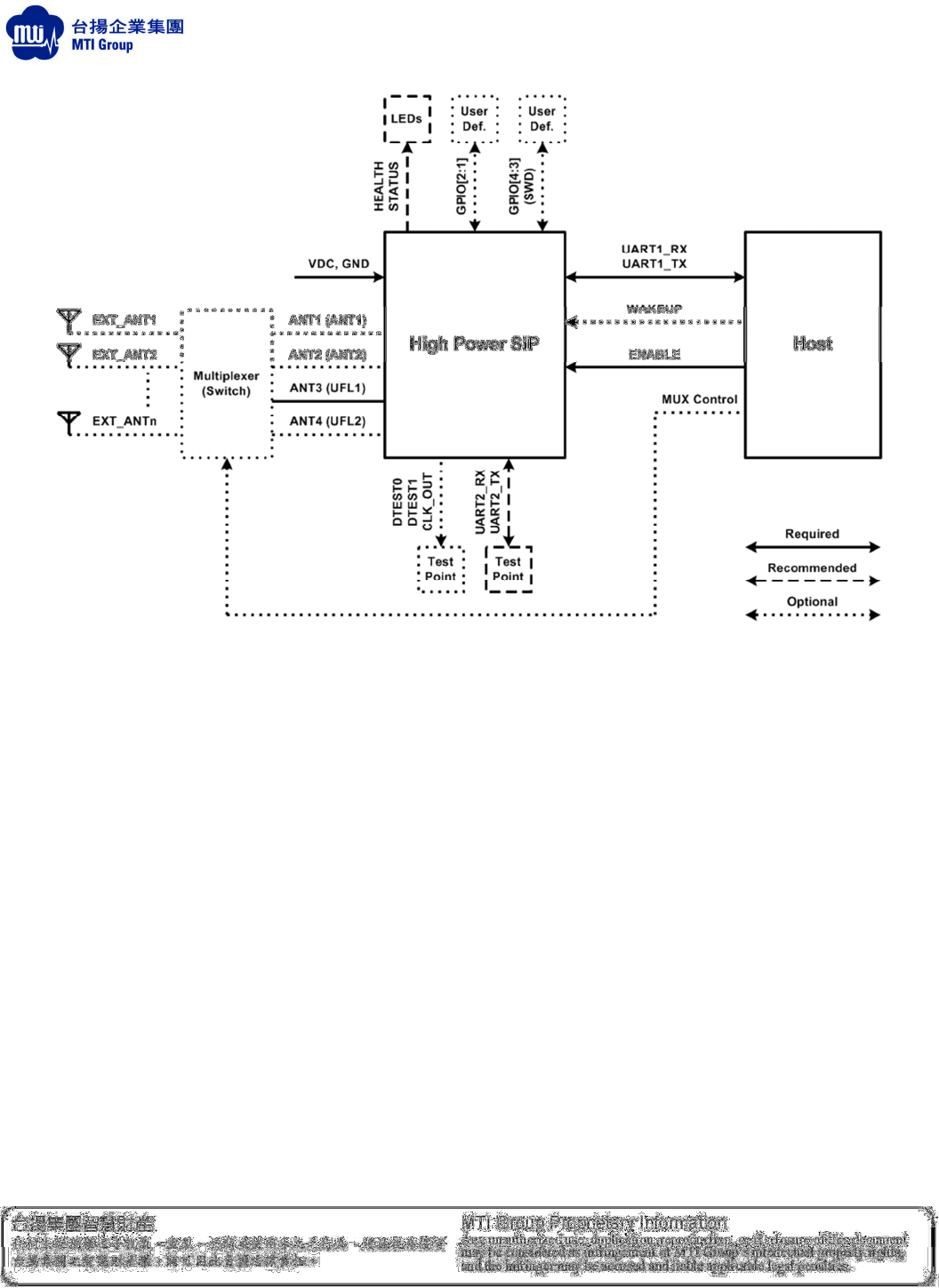
3.0 System Block Diagram
An example of a RU00-M03 system-level block diagram for an embedded application is shown in Figure 1.
Required connections:
VDC and GND are required to power the RU00-M03.
RF pin must be connected to the OEM antenna.
UART1 provides host communications to control the operation of the RU00-M03.
ENABLE pin resets the RU00-M03 when set low.
Recommended connections:
UART2 provides debug information.
HEALTH indicates successful boot of the RU00-M03. Connection to an LED provides a visual indication
of whether or not an error condition exists.
STATUS provides an indication when the RU00-M03 is inventorying tags. Connection to an LED
provides a visual indicator of the tag activity.
Optional connections:
GPIO allow the user to provide general-purpose user-controlled digital I/O
WAKEUP is a digital input which may wake the RU00-M03 from its sleep mode, the lowest power state
of the RU00-M03 (TBD).
Antenna port can be added by multiplexer (Switch).
Confidential Level(
安全
安全安全
安全等級
等級等級
等級
)
:
::
:
Low(
內部使用
內部使用內部使用
內部使用
)
RU00-M03 RFID High Power SiP Quick Guide PAGE: 7
43-RU00-M03-X001-01 DATE: 10-19-2018
Figure 1: System Block Diagram
Confidential Level(
安全
安全安全
安全等級
等級等級
等級
)
:
::
:
Low(
內部使用
內部使用內部使用
內部使用
)
RU00-M03 RFID High Power SiP Quick Guide PAGE: 8
43-RU00-M03-X001-01 DATE: 10-19-2018
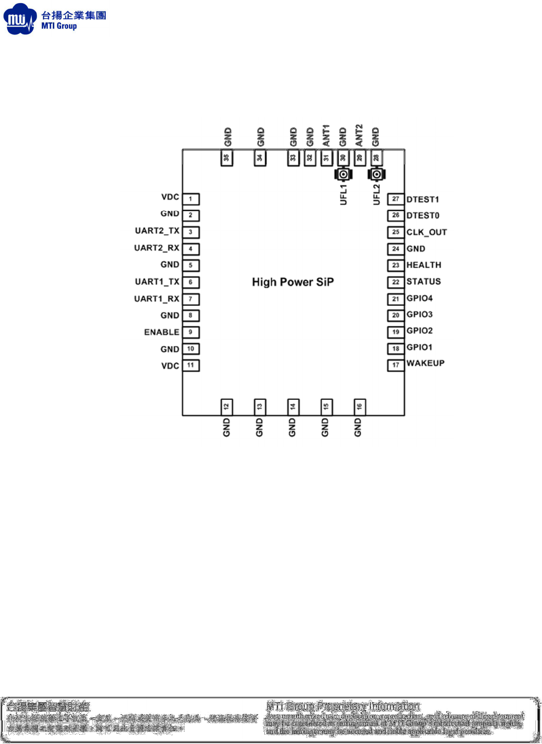
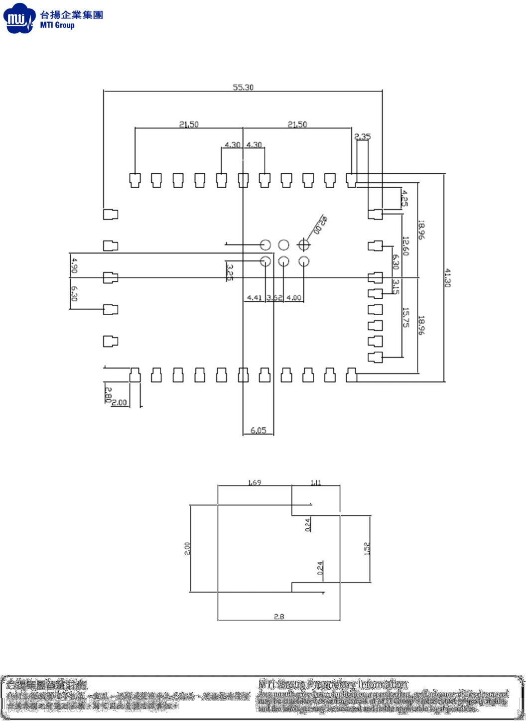
4.0 Pin Configurations and Descriptions
The module is 35-pin surface mount package (SMT compatible). The pin configurations are shown in
Figure
Figure 2: Pin Configurations
Confidential Level(
安全
安全安全
安全等級
等級等級
等級
)
:
::
:
Low(
內部使用
內部使用內部使用
內部使用
)
RU00-M03 RFID High Power SiP Quick Guide PAGE: 9
43-RU00-M03-X001-01 DATE: 10-19-2018
Pin
Number Pin Name Type Description
1 VDC Power Power Supply
2 GND Ground Ground
3 UART2_TX Output UART Debug Transmit Data
4 UART2_RX Input UART Debug Receive Data
5 GND Ground Ground
6 UART1_TX Output UART Console Transmit Data
7 UART1_RX Input UART Console Receive Data
8 GND Ground Ground
9 ENABLE Input Active High Enable Device
10 GND Ground Ground
11 VDC Power Power Supply
12,13,14,15,16 GND Ground Ground
17 WAKEUP Input Active High Wake up Device
18 GPIO1 I/O General Purpose Input/Output
19 GPIO2 I/O General Purpose Input/Output
20 GPIO3 I/O General Purpose Input/Output (*1)
21 GPIO4 I/O General Purpose Input/Output (*2)
22 STATUS Output Status Indication
23 HEALTH Output Status Indication
24 GND Ground Ground
25 CLK_OUT Output N/A
26 DTEST0 Output N/A
27 DTEST1 Output N/A
28 GND Ground Ground
29 ANT2 Output Monostatic antenna port 2 (*3)
30 GND Ground Ground
31 ANT1 Output Monostatic antenna port 1 (*3)
32,33,34,35 GND Ground Ground
UFL1 ANT3 Output Monostatic antenna port 3 (*3)
UFL2 ANT4 Output Monostatic antenna port 4 (*3)
Table 2: Pin Configurations
(*1) Pin 20: GPIO3 can be configured to SWDIO (Serial Wire Input/Output) for programming
Confidential Level(
安全
安全安全
安全等級
等級等級
等級
)
:
::
:
Low(
內部使用
內部使用內部使用
內部使用
)
RU00-M03 RFID High Power SiP Quick Guide PAGE: 10
43-RU00-M03-X001-01 DATE: 10-19-2018
(*2) Pin 21: GPIO4 can be configured to SWDIO (Serial Wire Input/Output) for programming
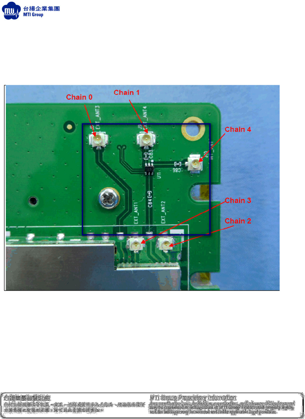
(*3) Antenna connections may be used via ANT1 (pin 31), ANT2 (pin 29) pads with 50Ω line on the
bottom of board and via U.FL connectors on the top of board named ANT3(UFL1) and ANT4(UFL2).
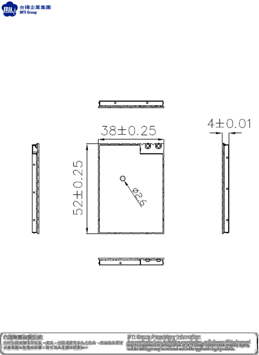
5.0 Package Information
Package Mechanical Outline
Figure 3: Package Mechanical Outline
Confidential Level(
安全
安全安全
安全等級
等級等級
等級
)
:
::
:
Low(
內部使用
內部使用內部使用
內部使用
)
RU00-M03 RFID High Power SiP Quick Guide PAGE: 11
43-RU00-M03-X001-01 DATE: 10-19-2018
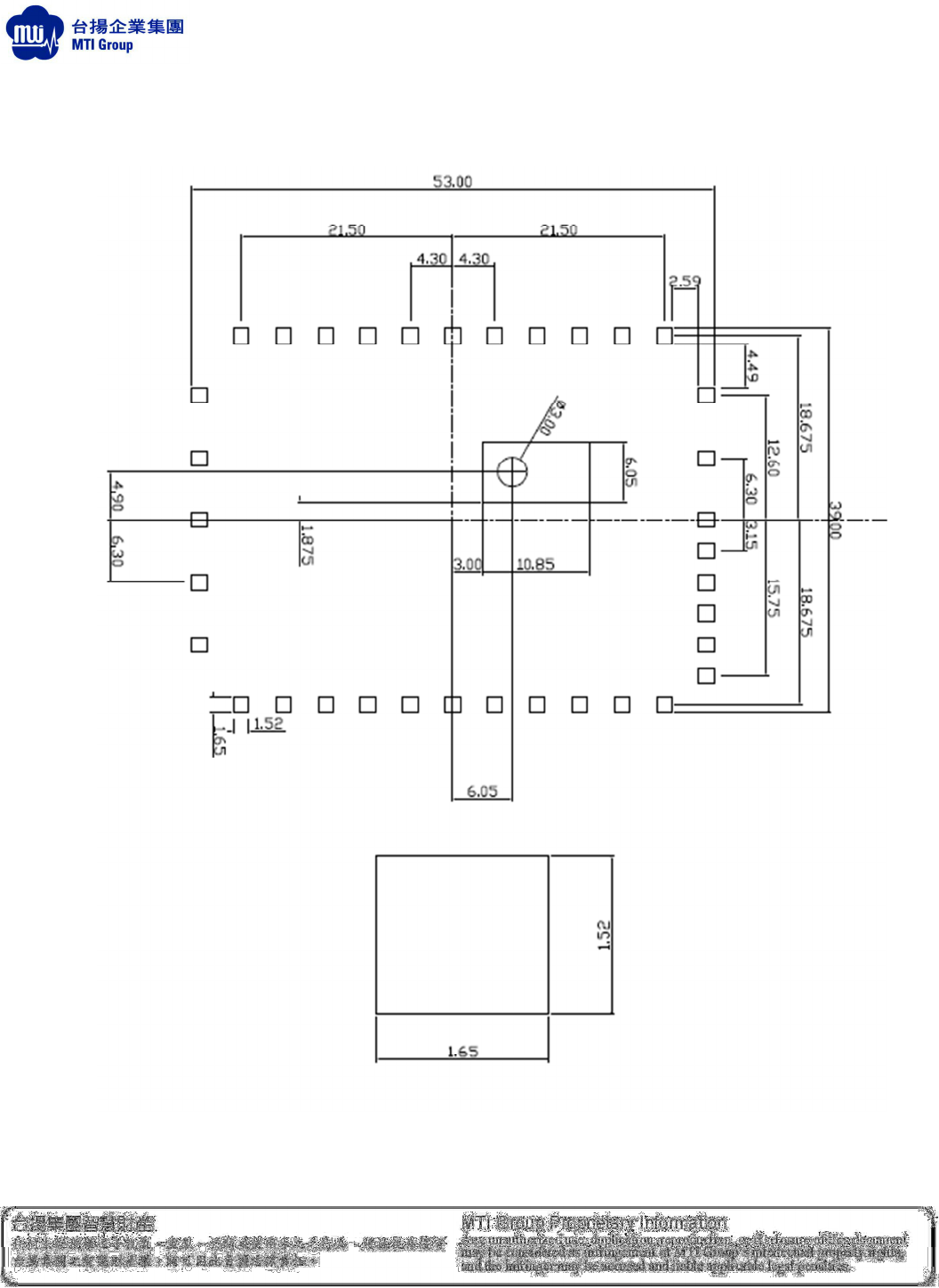
Recommend Footprint
Figure 4: Recommend Footprint
Confidential Level(
安全
安全安全
安全等級
等級等級
等級
)
:
::
:
Low(
內部使用
內部使用內部使用
內部使用
)
RU00-M03 RFID High Power SiP Quick Guide PAGE: 12
43-RU00-M03-X001-01 DATE: 10-19-2018
Recommend Stencil
\
Figure 5: Recommend Stencil

Confidential Level(
安全
安全安全
安全等級
等級等級
等級
)
:
::
:
Low(
內部使用
內部使用內部使用
內部使用
)
RU00-M03 RFID High Power SiP Quick Guide PAGE: 13
43-RU00-M03-X001-01 DATE: 10-19-2018
6.0 Interfacing to the RU00-M03
Power and Ground
All circuits on the RU00-M03 are powered from inputs at pin 1 and 11. The RU00-M03 operates with any
supply voltage between 3.2 and 5.25V. Because the individual supplies within the part are regulated on the
RU00-M03, a large amount of supply filtering is not required. A high value, low ESR tantalum capacitor
(150uF or greater) is recommended and should be accompanied by a 0.1uF ceramic chip capacitor close to
the pin.
All 16 available ground pins of the RU00-M03 must be soldered to the user PCB per the recommended
assembly guidelines. If the PCB utilizes separate analog/RF and digital grounds, it is recommended that the
RU00-M03 connect to the analog/RF ground. Providing a highly conductive path from the SiP ground to a
continuous ground plane (by use of numerous vias to the ground plane) and as much ground conductor
area as possible on the outer layers of the user PCB will help to reduce the RU00-M03 temperature rise
during operation.
Communication
The RU00-M03 has two UART ports, each of which utilizes 3.3V CMOS I/O over a pair of pins. The UARTs are
compatible with a standard RS-232C serial port through an appropriate level translator IC. The user’s host
processor issues IRI commands to the HOST UART (RX pin 7, TX pin 6), which can be configured for any
standard UART data rate for 115.2k, 230.4k, 460.8k and 921.6 kbaud. The default rate is set to 115.2 kbaud.
The DEBUG UART (RX pin 4, TX pin 3) is available to provide status information from the RU00-M03
microcontroller. The DEBUG UART is not required for RU00-M03 reader applications and should be
operated at a fixed data rate of 115.2 kbaud. Please see the RU00-M03data sheet for detailed I/O
specifications.
RF
The RU00-M03 is configured for monostatic operation, which requires only a single RF I/O pin for full duplex
communication. The output must be routed to the antenna via 50 ohm microstrip or stripline on the OEM
PCB. No coupling capacitor is required given that the RF pin is AC-coupled internal to the RU00-M03. To
maximize the radiated power (and corresponding communication range), the length of the transmission line
between RU00-M03 and antenna should be made as short as possible.
GPIO

Confidential Level(
安全
安全安全
安全等級
等級等級
等級
)
:
::
:
Low(
內部使用
內部使用內部使用
內部使用
)
RU00-M03 RFID High Power SiP Quick Guide PAGE: 14
43-RU00-M03-X001-01 DATE: 10-19-2018
There are four user-configurable digital GPIOs on the RU00-M03. The signals are number GPIO1 – GPIO4
and occupy pins 17 – 20 respectively. Each GPIO operates at standard 3.3V CMOS logic levels with a
minimum output current capability of 4 mA per pin while maintaining guaranteed noise margins.
Appropriate interface circuitry and layout as well as handling of the OEM hardware should be applied.
Please see the RU00-M03 data sheet for detailed I/O specifications.
Enable
Pin 9 of the RU00-M03 comprises the ENABLE signal. The RU00-M03 is held in reset if the signal is held low.
The ENABLE signal is bidirectional and is pulled down to 3.3V by ~10kΩ resistance internal to the RU00-M03.
Any external connection to this pin must maintain a low impedance (<<10kΩ) other than when an external
reset signal is applied. This allows the RU00-M03 to exert control of the reset line during power up and
other situations that require it.
Health and Status
RU00-M03 pin 22 is a dedicated digital output that indicates the HEALTH of the RU00-M03. After the
RU00-M03 is successfully booted and in its operational state, the health output switches to low. Otherwise,
the output is high. The OEM can digitally monitor this signal or use it to drive an LED for visual indication of
the RU00-M03 health.
Pin 23 is a dedicated digital output that indicates the tag inventory STATUS of the RU00-M03. When the
RU00-M03 is successfully inventorying one or more tags, it will generate 0.5ms minimum high pulse. The
output remains low when no tags are being inventoried. Like the health signal, the OEM can monitor it via
firmware or use it to drive an LED for visual indication to the device user.

Confidential Level(
安全
安全安全
安全等級
等級等級
等級
)
:
::
:
Low(
內部使用
內部使用內部使用
內部使用
)
RU00-M03 RFID High Power SiP Quick Guide PAGE: 15
43-RU00-M03-X001-01 DATE: 10-19-2018
7.0 Operating the RU00-M03
Once the required hardware connections are made to the RU00-M03, the unit can be operated with simple
software routines running on the OEM’s host processor. The host software issues commands to configure
the reader, set the reader’s idle mode and to start and stop various Gen2 RFID reader operations.
An example of the sequence of events starting at reader power-up is:
1. Apply 3.2V~5.25V power to the RU00-M03.
2. Establish a connection to the device via the host software.
3. Configure the reader. Critical parameters are:
a. Region of operation
When configured for a specific region, the RU00-M03 can operate only according to the air interface
standards for that region. Key communication parameters are not adjustable by the user but are
inherent in the RU00-M03 firmware. The FCC regional operation is the default for the device.
NOTE: The OEM is strictly forbidden to operate the RU00-M03 in a regional mode other than that in
which the device is located. Applicable agency certification must be obtained by the OEM for their
product to operate in the region in which it is located. The modular certification of the RU00-M03 in
the U.S. may only be utilized by OEM’s that follow all guidelines set forth in this document.
b. RF output power
The RU00-M03 output power must be set to a level between 10 and 30dBm. The default power is set
to the reader’s maximum allowable of 30dBm.
4. Initiate an RFID operation.
Gen2 RFID operations including Inventory, Read, Write, Lock and Kill are initiated with a command.
5. Set the RU00-M03 standby mode.
When the RU00-M03 is not executing an RFID operation, it assumes a low power state until another RFID
function is initiated by the host.
Confidential Level(
安全
安全安全
安全等級
等級等級
等級
)
:
::
:
Low(
內部使用
內部使用內部使用
內部使用
)
RU00-M03 RFID High Power SiP Quick Guide PAGE: 16
43-RU00-M03-X001-01 DATE: 10-19-2018
8.0 Regulatory Guidelines
OEM shall follow the below design guidelines for KDB 993369
1. Trace layout and dimensions including specific designs for each type:
a. For the chain 2 and chain 3, it can be connected 50 ohm UFL mapping connector to external
antenna
b. For chain 0, it is connected via microstrip trace, please design guide as below.
c. For chain 1 and chain 4, it is connected via microstrip trace and insert a single pole two through
switch. The parameters in portion of transmission line are same as chain 0. The RF Switch is also 50
ohm characteristic and isolation is at least 20dB. It is equivalent to passive part. It always transmits
one path at one time during operating.
Confidential Level(
安全
安全安全
安全等級
等級等級
等級
)
:
::
:
Low(
內部使用
內部使用內部使用
內部使用
)
RU00-M03 RFID High Power SiP Quick Guide PAGE: 17
43-RU00-M03-X001-01 DATE: 10-19-2018
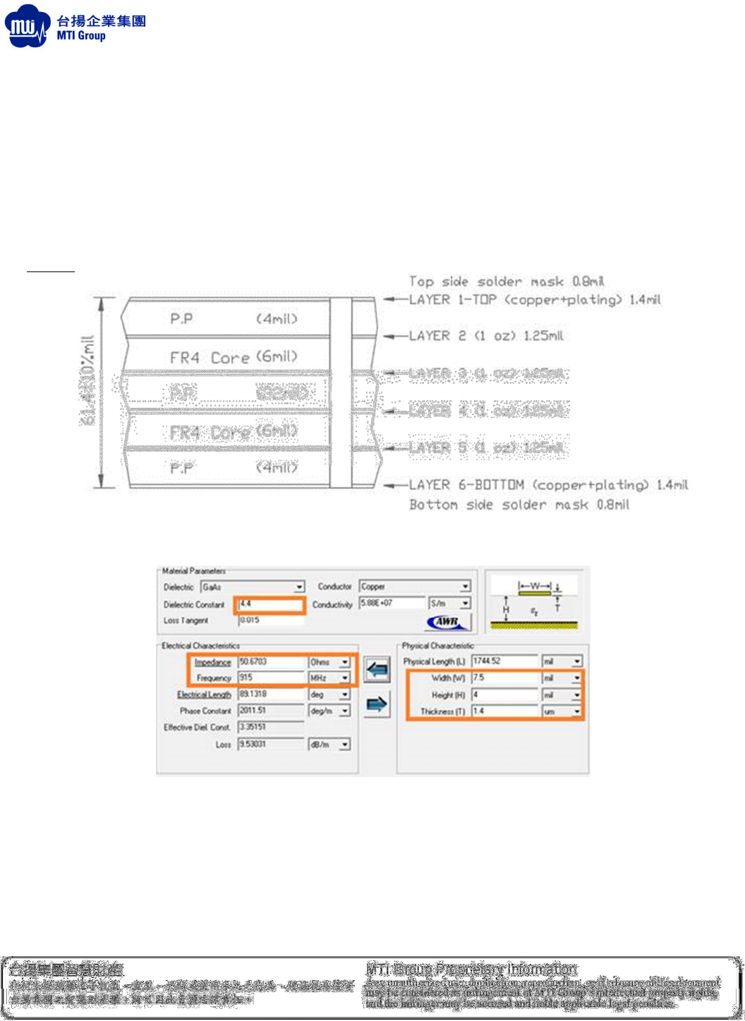
The RU00-M03 is designed for 50 +/- 10% Ohm characteristic impedance, and the connection between
RU00-M03 and antenna should all be designed for 50 Ohm characteristic impedance. For connection to
external antenna via connectors, user should design the PCB layout for 50 Ohm characteristic
impedance using microstrip, stripline, etc.
For example, user can design Microstrip according to PCB stack up (shown in below figure) by tool
TXLINE (Transmission Line Calculator) to get PCB path width for RF is 7.5mil.
The detail parameters such as operating center frequency, RF impedance, dialectical constant, trace
width, height of PCB Copper thickness. Please see the below figure.
2. Appropriate parts by manufacturer and specifications.
All parts from RF I/O interface of module to antenna shall meet characteristic impedance of 50 ohms +/-
10%.
a. The connector on OEM’s PCB with interfaces to antenna must be 50ohm characteristic impedance

Confidential Level(
安全
安全安全
安全等級
等級等級
等級
)
:
::
:
Low(
內部使用
內部使用內部使用
內部使用
)
RU00-M03 RFID High Power SiP Quick Guide PAGE: 18
43-RU00-M03-X001-01 DATE: 10-19-2018
as well. The following connectors are allowed.
- Ultra UMCC Jack : Hirose electric, model U.FL-R-SMT-1 or equivalent
- SMA Jack : Aliner Industries, model 20-001DW-T or equivalent.
- Other 50ohm characteristic impedance equivalent RF connector
b. It supports to add multiplexer (RF Switch) between transmission line and connector on OEM’s PCB.
- RF switch: Skyworks, model SKY13270-92LF or equivalent.
c. The cable between qualified antenna and connector shall use 50 ohm coaxial pigtail from connector
of PCB to antenna.
d. The OEM must strictly use only with the following antennas or antenna types with maximum gain as
shown.
- American RFID solution, model HD-500 circular polarization antenna with 6dBi gain
- Microelectronics Technology Inc, model RFID0900 circular polarization antenna with 6dBi gain
- BroadRadio, model BRA-07 circular polarization antenna with 3dBiC
3. Test procedures for design verification.
-OEM shall follow transmission line design rule for characteristic impedance of 50 ohms +/- 10%.
-OEM needs to measure transmission line width on PCB to ensure the impedance is 50 ohms +/- 10%
4. Production test procedures for ensuring compliance
The 50 ohm transmission line and connector are passive parts, it is an attenuation in system. Once OEM has
confirmed the impedance in design verification, OEM can measure output power via connector instead of
transmission impedance measurement.
-Connect cable with connector on OEM’s PCB to RF power meter or equivalent.
-Execute OEM’s product to transmit output power and measure output power.