MitraStar Technology M4G-641 M4G-641 LTE FDD MODULE User Manual User Guide
MitraStar Technology Corporation M4G-641 LTE FDD MODULE User Guide
User Guide
© 2012 MitraStar Technology Corp. All Rights Reserved. Ver. 1.2
3GPPTS 36.521 Compliant
(LTE FDD)
R8. Software upgradable to
R9
FDD Dual Band
Band 13
Band 4
Standard mPCIe minicard
Form Factor
23dBm Transmission Power
Wireless Broadband LTE Solutions
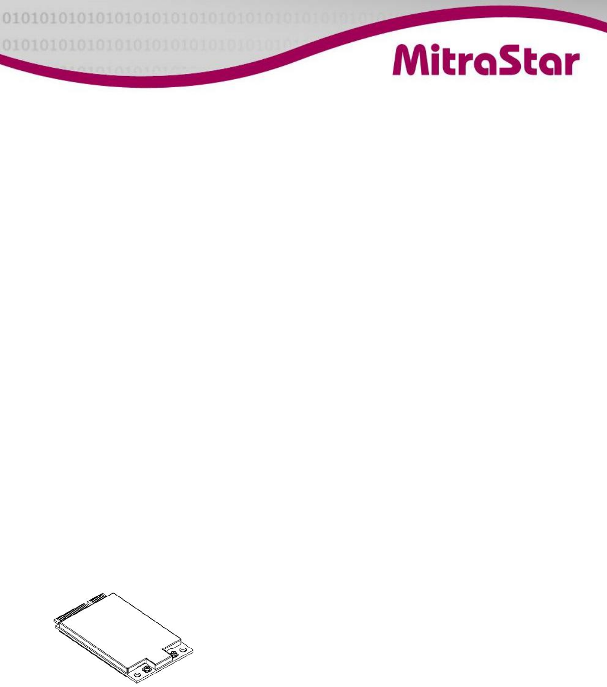
MitraStar M4G-641 LTE FDD Module
Band 13 & Band 4 supported
Field Proved LTE Technology
M4G-641 is based on Altair Semiconductor’s high performance LTE chipsets of
FourGee3100 baseband and FourGee6202 RFIC chip. It supports 3GPP R8 and R9
upgradable without hardware change. It supports LTE connection using single
software and implements a high performance MIMO receiver. Altair FourGee
3100/6202 LTE chipset is Verizon Wireless pre-certified to run over Verizon’s 4G
LTE network.
Fast Hook Up Standard Minicard Interface
M4G-641 adapts the standard mini-PCIe minicard with 52 pin connector. The
dimension is 51(L) x 30(W) x 5(H)mm. Both sides have components. Two antenna
connectors are provided. The operation temperature ranged from -30°C to 60°C.
Easy Enable with Hostless Driver Support
M4G-641 supports hostless driver architecture on Linux and Windows. The
advantage of this kind of driver requires a lower-end process to establish LTE
connection and run traffic through LTE network. This will let most lower-end
machine-to-machine applications to use 4G wireless broadband LTE high speed
network in the first moment.

© 2012 MitraStar Technology Corp. All Rights Reserved. Ver. 1.2
Specifications
LTE Air Interface
3GPPTS 36.521 Compliant
R8 compliance
Software upgradeable to R9.
Duplex mode: FDD
Band 13
Uplink 777-787MHz
Downlink 746-756MHz
Band 4
Uplink 1710-1755 MHz
Downlink 2110-2155 MHz
Channel Bandwidth:
1.4MHz, 3MHz, 5MHz, 10MHz,
15MHz and 20MHz.
Modulation:
Uplink QPSK, 16QAM
Downlink QPSK, 16QAM, 64QAM
Transmsit Power : 23±1 dBm
Receive Sensitivity:
-97dBm @ QPSK 1/2. 10MHz
channel bandwidth
Antenna:
Two antenna connectors
Main RF for transmit & receive
Auxiliary RF for receive diversity
Hardware Specifications
mini-PCIe minicard 52 connector
(work in USB mode)
LED : Power/ LTE connection
status through minicard interface
SIM card though mini-card
interface
Power Specification
Input Voltage: 3.3V ± 9%
Power consumption :
Average power consumption 3 W
Physical Specifications
Dimension:
51(L) x 30(W) x 5(H)mm
Weight: 12g
Environmental Specifications
Operation Temperature: -30 oC ~
60oC
Operation Humidity : 10% ~ 90%
Storage Temperature: -30oC ~
70oC
Storage Humidity: 10% ~ 95%
OS Support
Linux
Microsoft Windows
Certification
FCC
RoHS
© 2012 MitraStar Technology Corp. All Rights Reserved. Ver. 1.2
Pin Assignment
Pin Number Minicard
Standard
Pin Define
I/O MitraStar
LTE module
Pin Definition
I/O Description
1 WAKE_N O NC - No Connect
2 3V3_Vaux I 3V3_Vaux I Main Board for Module +3V3 System
3 COEX1/NC I/O BUZZER_CTL O USB Mode: no used
OP Mode: RSSI Signal Monitor by Voice
4 GND I GND I Ground
5 COEX2/NC I/O RSSI_LED_0 O USB Mode: no used
OP Mode: RSSI Signal Monitor by LED
6 1.5V I NC - No Connect
7 CLKREQ_N O LAN_RESET O OP Mode: Rest PHY IC
USB Mode: no used
8 UIM_PWR O UIM_PWR O For SIM Slot (Card) Power +1.8V/+3.0V
9 GND I GND I Ground
10 UIM_DATA I/O UIM_DATA I/O SIM Data Signal
11 REF_CLK- I NC - No Connect
12 UIM_CLK O UIM_CLK O SIM Clock Signal
13 REF_CLK+ I NC - No Connect
14 UIM_RST O UIM_RST O SIM Reset Signal
15 GND I GND I Ground
16 UIM_VPP O NC - No Connect
17 UIM_C8 NA NC - No Connect
18 GND I GND I Ground
19 UIM_C4 NA NC - No Connect
20 W_DISABLE_N I W_DISABLE_N I USB Mode: Active Low Signal. System Can Be Use This Signal
to Disable Radio Operation. Pull-up Resistor on The Card.
(Feature Support)
Low: Idle/Sleep Mode
High: Operation Mode
OP Mode: no used
21 GND I GND I Ground
22 PERST_N I PERST_N I USB Mode: Reset Module
OP Mode: no used
23 PERn0 I/O RMII_RXCTL I OP Mode: RMII Interface
USB Mode: no used
24 3V3_Vaux I 3V3_Vaux I Main Board for Module +3V3 System
25 PERp0 I/O RMII_TXCTL O OP Mode: RMII Interface
USB Mode: no used
26 GND I GND I Ground
© 2012 MitraStar Technology Corp. All Rights Reserved. Ver. 1.2
Pin Number Minicard
Standard
Pin Define
I/O MitraStar
LTE module
Pin Definition
I/O Description
27 GND I GND I Ground
28 1.5V I NC - No Connect
29 GND I GND I Ground
30 SMB_CLK I RMII_MDIO I/O OP Mode: RMII Interface
USB Mode: no used
31 PETn0 I/O RMII_RXD0 I OP Mode: RMII Interface
USB Mode: no used
32 SMB_DATA I/O RMII_MDC O OP Mode: RMII Interface
USB Mode: no used
33 PETp0 I/O RMII_RXD1 I OP Mode: RMII Interface
USB Mode: no used
34 GND I GND I Ground
35 GND I GND I Ground
36 USB_D- I/O USB_D- I/O OP Mode: no used
USB Mode: Data Interface
37 GND I GND I Ground
38 USB_D+ I/O USB_D+ I/O OP Mode: no used
USB Mode: Data Interface
39 3V3_Vaux I 3V3_Vaux-PA I Main Board for PA Power +3V3 (+23dBm) or +4V2 (+26dBm)
40 GND I GND I Ground
41 3V3_Vaux I 3V3_Vaux-PA I Main Board for PA Power +3V3 (+23dBm) or +4V2 (+26dBm)
42 LED_WWAN_N O RSSI_LED_1 X USB Mode: no used
OP Mode: RSSI Signal Monitor by LED
43 GND I GND I Ground
44 LED_WLAN_N O RSSI_LED_2 O USB Mode: no used
OP Mode: RSSI Signal Monitor by LED
45 NC X RMII_CLK O OP Mode: RMII Interface
USB Mode: no used
46 LED_WPAN_N O NC - No Connect
47 NC X RMII_TXD0 O OP Mode: RMII Interface
USB Mode: no used
48 1.5V I NC - No Connect
49 NC X RMII_TXD1 O OP Mode: RMII Interface
USB Mode: no used
50 GND I GND I Ground
51 NC X NC - No Connect
52 3V3_Vaux I 3V3_Vaux-PA I Main Board for PA Power +3V3 (+23dBm) or +4V2 (+26dBm)
© 2012 MitraStar Technology Corp. All Rights Reserved. Ver. 1.2
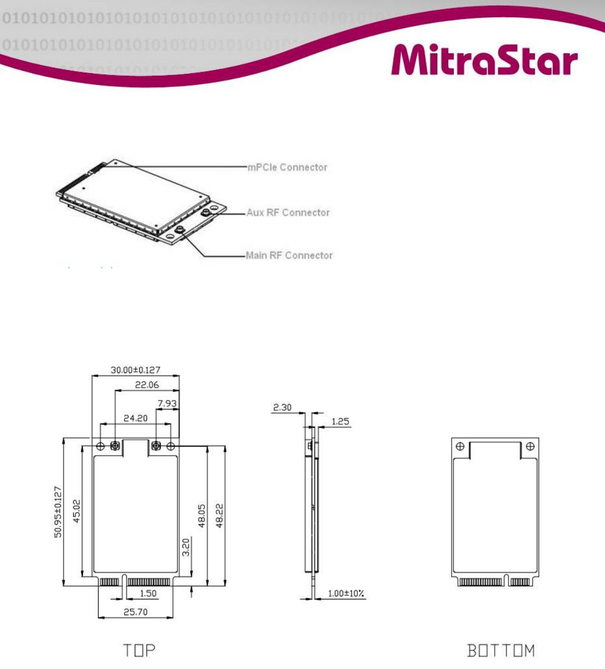
Connector
Figure 1 Module Connectors
Physical Dimension
Figure 2 Mechanical Drawing (unit: mm)

© 2012 MitraStar Technology Corp. All Rights Reserved. Ver. 1.2
Manual Information to the End User
The OEM integrator has to be aware not to provide information to the end user regarding how to install or remove this RF
module in the user’s manual of the end product which integrates this module. The end user manual shall include all
required regulatory information/warning as show in this manual.
Federal Communication Commission Interference Statement
This device complies with Part 15 of the FCC Rules. Operation is subject to the following two conditions: (1) This device
may not cause harmful interference, and (2) this device must accept any interference received, including interference that
may cause undesired operation.
This equipment has been tested and found to comply with the limits for a Class B digital device, pursuant to Part 15 of the
FCC Rules. These limits are designed to provide reasonable protection against harmful interference in a residential
installation. This equipment generates, uses and can radiate radio frequency energy and, if not installed and used in
accordance with the instructions, may cause harmful interference to radio communications. However, there is no
guarantee that interference will not occur in a particular installation. If this equipment does cause harmful interference
to radio or television reception, which can be determined by turning the equipment off and on, the user is encouraged to
try to correct the interference by one of the following measures:
- Reorient or relocate the receiving antenna.
- Increase the separation between the equipment and receiver.
- Connect the equipment into an outlet on a circuit different from that to which the receiver is connected.
- Consult the dealer or an experienced radio/TV technician for help.
Any changes or modifications not expressly approved by the party responsible for compliance could void the user's
authority to operate this equipment. This transmitter must not be co-located or operating in conjunction with any other
antenna or transmitter.
Radiation Exposure Statement
This equipment complies with FCC radiation exposure limits set forth for an uncontrolled environment. This equipment
should be installed and operated with minimum distance 20 cm between the radiator & your body.
End Product Labeling
When the module is installed in the host device, the FCC ID label must be visible through a window on the final device or
it must be visible when an access panel, door or cover is easily re-moved. If not, a second label must be placed on the
outside of the final device that contains the following text: “Contains FCC ID: ZMYM4G-641”
The grantee's FCC ID can be used only when all FCC compliance requirements are met.

© 2012 MitraStar Technology Corp. All Rights Reserved. Ver. 1.2
This device is intended only for OEM integrators under the following conditions:
(1) The antenna must be installed such that 20 cm is maintained between the antenna and users,
(2) The transmitter module may not be co-located with any other transmitter or antenna.
(3) To comply with FCC regulations limiting both maximum RF output power and human exposure to RF radiation, the
maximum antenna gain including cable loss in a mobile exposure condition must not exceed:
5.5dBi in LTE Band 4
10dBi in LTE Band 13
In the event that these conditions cannot be met (for example certain laptop configurations or co-location with another
transmitter), then the FCC authorization is no longer considered valid and the FCC ID cannot be used on the final product.
In these circumstances, the OEM integrator will be responsible for re-evaluating the end product (including the
transmitter) and obtaining a separate FCC authorization.