Mitsumi Electric WML-C06 WML-C06 Bluetooth User Manual Functional Description fcc r1 0
Mitsumi Electric Co., Ltd. WML-C06 Bluetooth Functional Description fcc r1 0
UserManual.wiki
>
Mitsumi Electric
>
WML C06 User Manual
technical description
Navigation menu
Upload a User Manual
Namespaces
Wiki Guide
HTML
PDF
Info
Views
User Manual
Discussion / Help
Navigation
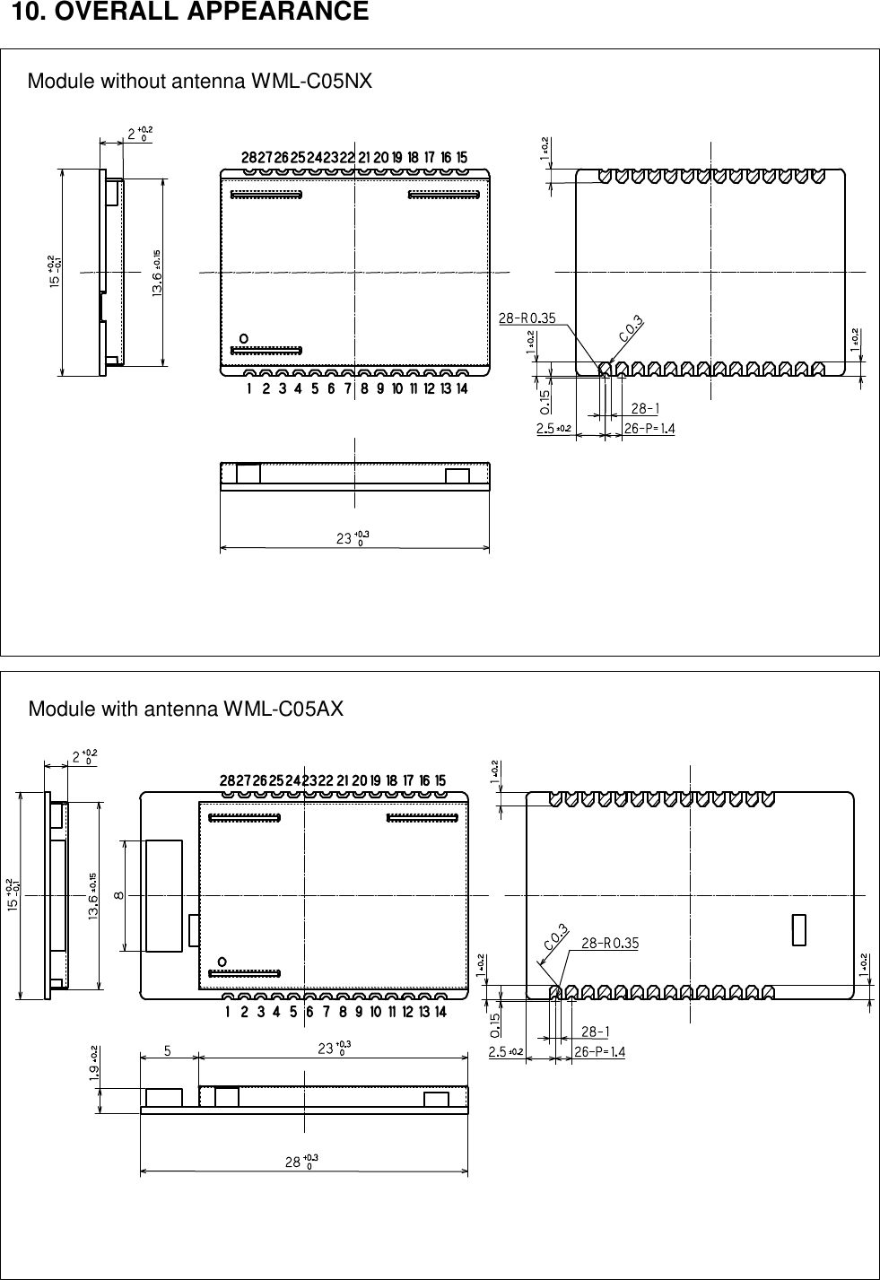
![5. TERMINAL DESCRIPTION No. Symbol I/O Description 1 PIO [0] / RXEN O Control output for external LNA (=PIO [0] ) 2 PIO [1] / TXEN O Control output for external PA (=PIO [1] ) 3 GND Ground 4 GND Ground 5 PIO [4] / IRQ1 I/O Programmable I/O line/Interrupt request1 6 PIO [5] / IRQ2 I/O Programmable I/O line/Interrupt request2 7 PIO [6] I/O Programmable I/O line 8 PIO [7] I/O Programmable I/O line 9 PCM_OUT O Synchronous PCM data out 10 PCM_CLK I/O Synchronous PCM data clock 11 PCM_IN I Synchronous PCM data input 12 PCM_SYNC I/O Synchronous data strobe 13 GND Ground 14 VDD Supply voltage 3.0 15 GND Ground 16 SPI_CSB I Chip select for Synchronous Serial Interface 17 SPI_MOSI I Synchronous Serial Interface data input 18 SPI_CLK I Synchronous Serial Interface Clock 19 SPI_MISO O Synchronous Serial Interface data output 20 UART_CTS/USB_D- I Asynchronous serial data CTS/USB Data- 21 UART_RTS/USB_D+ O Asynchronous serial data RTS/USB Data+ 22 UART_RX I Asynchronous serial data input 23 UART_TX O Asynchronous serial data output 24 PIO [3] I/O Data line for EEPROM 25 PIO [2] I CLOCK for EEPROM 26 RST I Not Available 27 GND Ground 28 ANT I/O RF input/output](https://usermanual.wiki/Mitsumi-Electric/WML-C06/User-Guide-157014-Page-2.png)
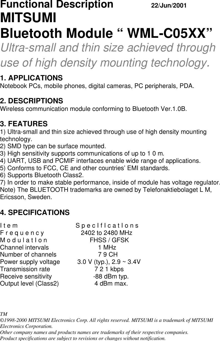
![6. BLOCK DIAGRAM 7. PCM IF PCM_OUT, PCM_IN, PCM_CLK, PCM_SYNC carry one of bi-directional channel of voice data using 13bits PCM at 8ks/s. PCM_SYNC operates at a fixed clock frequency of 8kHz. PCM_CLK operates at a fixed clock frequency of 256kHz. Bits 1 to 13 of the PCM_OUT data carry the current output sample value. Bits 14 to 16 carry a three bit signal level value. Reference PCM audio device is MC145483. 8. PIO PORT The PIO port is general purpose IO interface and the ports consists of 8 programmable, Bi-directional PIO [0:7]. The maximum current drive capability is 4mA. PIO [0], PIO [1] are recommended to be open if they are not used. UART/ USB UART_TX UART_RX UART_RTS/USB D+ UART_CTS/USB D- SPI_CSB SPI_CLK SPI_MOSI SPI_MISO PCM_OUT PCM_IN PCM_SYNC PCM_CLK SPI PCM/IF MEMORY DRIVER PIO FLASH ROM 256kx16 RAM RF Receiver RF Transmitter 1st Synthesizer Baseband- Controller Memory- Management 2nd Synthesizer REG 16bits Micro- Processor XT Driver 16MHz VDD ANT BPF SW TX_EN RX_EN BC01b1 Balun PIO [0], … ,PIO [7]](https://usermanual.wiki/Mitsumi-Electric/WML-C06/User-Guide-157014-Page-3.png)