Mitsumi Electric WML-C06 WML-C06 Bluetooth User Manual Functional Description fcc r1 0
Mitsumi Electric Co., Ltd. WML-C06 Bluetooth Functional Description fcc r1 0
technical description
Functional Description 22/Jun/2001
MITSUMI
Bluetooth Module “ WML-C05XX”
Ultra-small and thin size achieved through
use of high density mounting technology.
1. APPLICATIONS
Notebook PCs, mobile phones, digital cameras, PC peripherals, PDA.
2. DESCRIPTIONS
Wireless communication module conforming to Bluetooth Ver.1.0B.
3. FEATURES
1) Ultra-small and thin size achieved through use of high density mounting
technology.
2) SMD type can be surface mounted.
3) High sensitivity supports communications of up to 1 0 m.
4) UART, USB and PCMIF interfaces enable wide range of applications.
5) Conforms to FCC, CE and other countries’ EMI standards.
6) Supports Bluetooth Class2.
7) In order to make stable performance, inside of module has voltage regulator.
Note) The BLUETOOTH trademarks are owned by Telefonaktiebolaget L M,
Ericsson, Sweden.
4. SPECIFICATIONS
I t e m S p e c I f I c a t I o n s
F r e q u e n c y 2402 to 2480 MHz
M o d u l a t I o n FHSS / GFSK
Channel intervals 1 MHz
Number of channels 7 9 CH
Power supply voltage 3.0 V (typ.), 2.9 ~ 3.4V
Transmission rate 7 2 1 kbps
Receive sensitivity -88 dBm typ.
Output level (Class2) 4 dBm max.
TM
©1998-2000 MITSUMI Electronics Corp. All rights reserved. MITSUMI is a trademark of MITSUMI
Electronics Corporation.
Other company names and products names are trademarks of their respective companies.
Product specifications are subject to revisions or changes without notification.

5. TERMINAL DESCRIPTION
No. Symbol I/O Description
1 PIO [0] / RXEN O Control output for external LNA (=PIO [0] )
2 PIO [1] / TXEN O Control output for external PA (=PIO [1] )
3 GND Ground
4 GND Ground
5 PIO [4] / IRQ1 I/O Programmable I/O line/Interrupt request1
6 PIO [5] / IRQ2 I/O Programmable I/O line/Interrupt request2
7 PIO [6] I/O Programmable I/O line
8 PIO [7] I/O Programmable I/O line
9 PCM_OUT O Synchronous PCM data out
10 PCM_CLK I/O Synchronous PCM data clock
11 PCM_IN I Synchronous PCM data input
12 PCM_SYNC I/O Synchronous data strobe
13 GND Ground
14 VDD Supply voltage 3.0
15 GND Ground
16 SPI_CSB I Chip select for Synchronous Serial Interface
17 SPI_MOSI I Synchronous Serial Interface data input
18 SPI_CLK I Synchronous Serial Interface Clock
19 SPI_MISO O Synchronous Serial Interface data output
20 UART_CTS/USB_D- I Asynchronous serial data CTS/USB Data-
21 UART_RTS/USB_D+ O Asynchronous serial data RTS/USB Data+
22 UART_RX I Asynchronous serial data input
23 UART_TX O Asynchronous serial data output
24 PIO [3] I/O Data line for EEPROM
25 PIO [2] I CLOCK for EEPROM
26 RST I Not Available
27 GND Ground
28 ANT I/O RF input/output
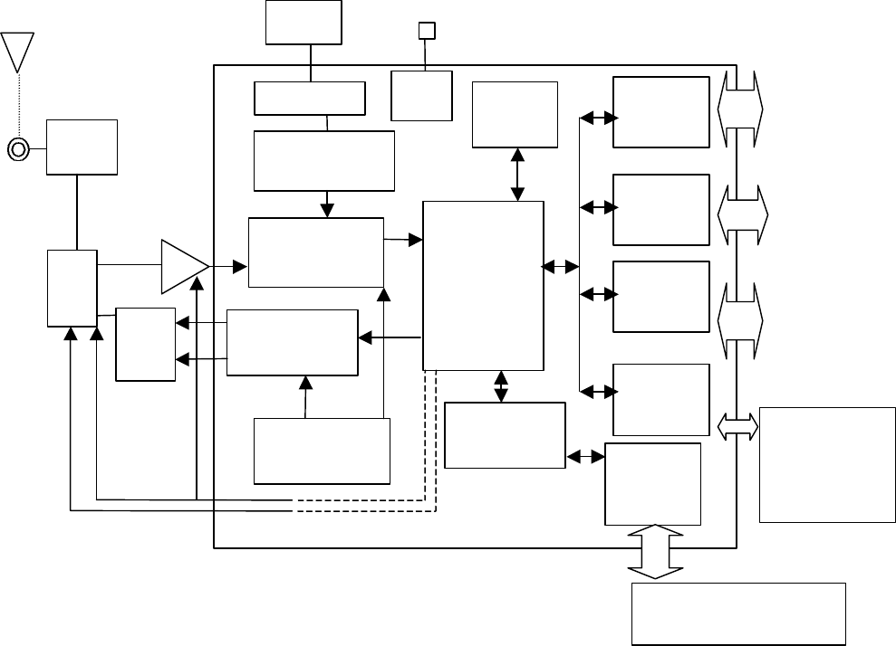
6. BLOCK DIAGRAM
7. PCM IF
PCM_OUT, PCM_IN, PCM_CLK, PCM_SYNC carry one of bi-directional channel of voice
data using 13bits PCM at 8ks/s.
PCM_SYNC operates at a fixed clock frequency of 8kHz.
PCM_CLK operates at a fixed clock frequency of 256kHz.
Bits 1 to 13 of the PCM_OUT data carry the current output sample value.
Bits 14 to 16 carry a three bit signal level value.
Reference PCM audio device is MC145483.
8. PIO PORT
The PIO port is general purpose IO interface and the ports consists of 8 programmable,
Bi-directional PIO [0:7]. The maximum current drive capability is 4mA.
PIO [0], PIO [1] are recommended to be open if they are not used.
UART/
USB
UART_TX
UART_RX
UART_RTS/USB
D+
UART_CTS/USB D-
SPI_CSB
SPI_CLK
SPI_MOSI
SPI_MISO
PCM_OUT
PCM_IN
PCM_SYNC
PCM_CLK
SPI
PCM/IF
MEMORY
DRIVER
PIO
FLASH
ROM
256kx16
RAM
RF Receiver
RF Transmitter
1st Synthesizer
Baseband-
Controller
Memory-
Management
2
nd
Synthesizer
REG
16bits Micro-
Processor
XT Driver
16MHz
VDD
ANT
BPF
SW
TX_EN
RX_EN
BC01b1
Balun
PIO [0], … ,PIO [7]

9. FCC Compliance and Advisory Statement
FCC Part 15.19)
This device complies with part 15 of the FCC Rules. Operation is subject to the following two
conditions: (1) This device may not cause harmful interference, and (2) this device must accept
any interference received, including interference that may cause undesired operation.
FCC Part 15.21 and 15.105)
Changes or modifications not expressly approved by the party responsible for compliance could
void the user's authority to operate the equipment.
Note: This equipment has been tested and found to comply with the limits for a Class B digital
device, pursuant to part 15 of the FCC Rules. These limits are designed to provide reasonable
protection against harmful interference in a residential installation. This equipment generates,
uses and can radiate radio frequency energy and, if not installed and used in accordance with
the instructions, may cause harmful interference to radio communications. However, there is no
guarantee that interference will not occur in a particular installation. If this equipment does
cause harmful interference to radio or television reception, which can be determined by turning
the equipment off and on, the user is encouraged to try to correct the interference by one or
more of the following measures:--Reorient or relocate the receiving antenna.--Increase the
separation between the equipment and receiver.--Connect the equipment into an outlet on a
circuit different from that to which the receiver is connected. --Consult the dealer or an
experienced radio/TV technician for help.
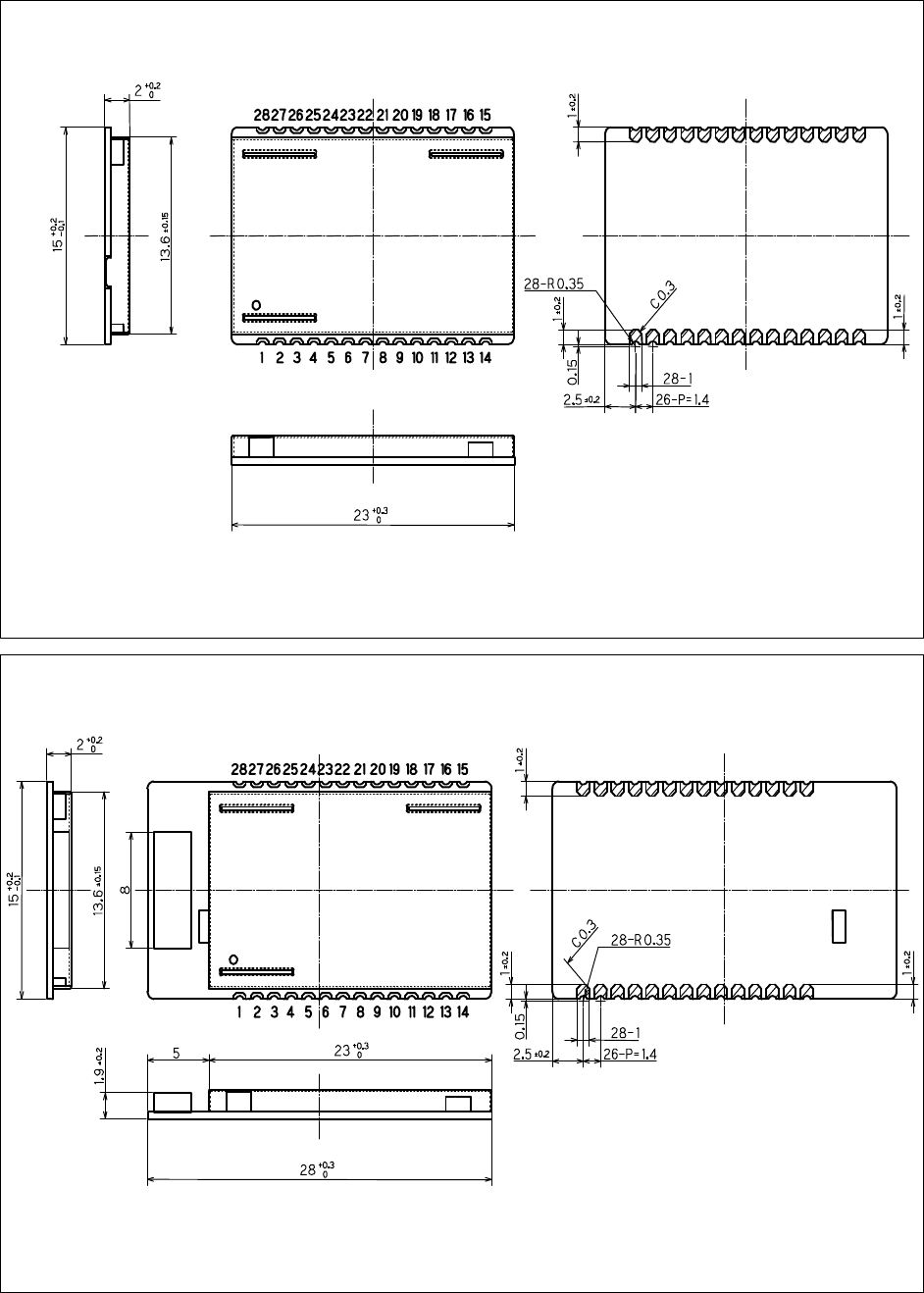
10. OVERALL APPEARANCE
Module without antenna WML-C05NX
Module with antenna WML-C05AX