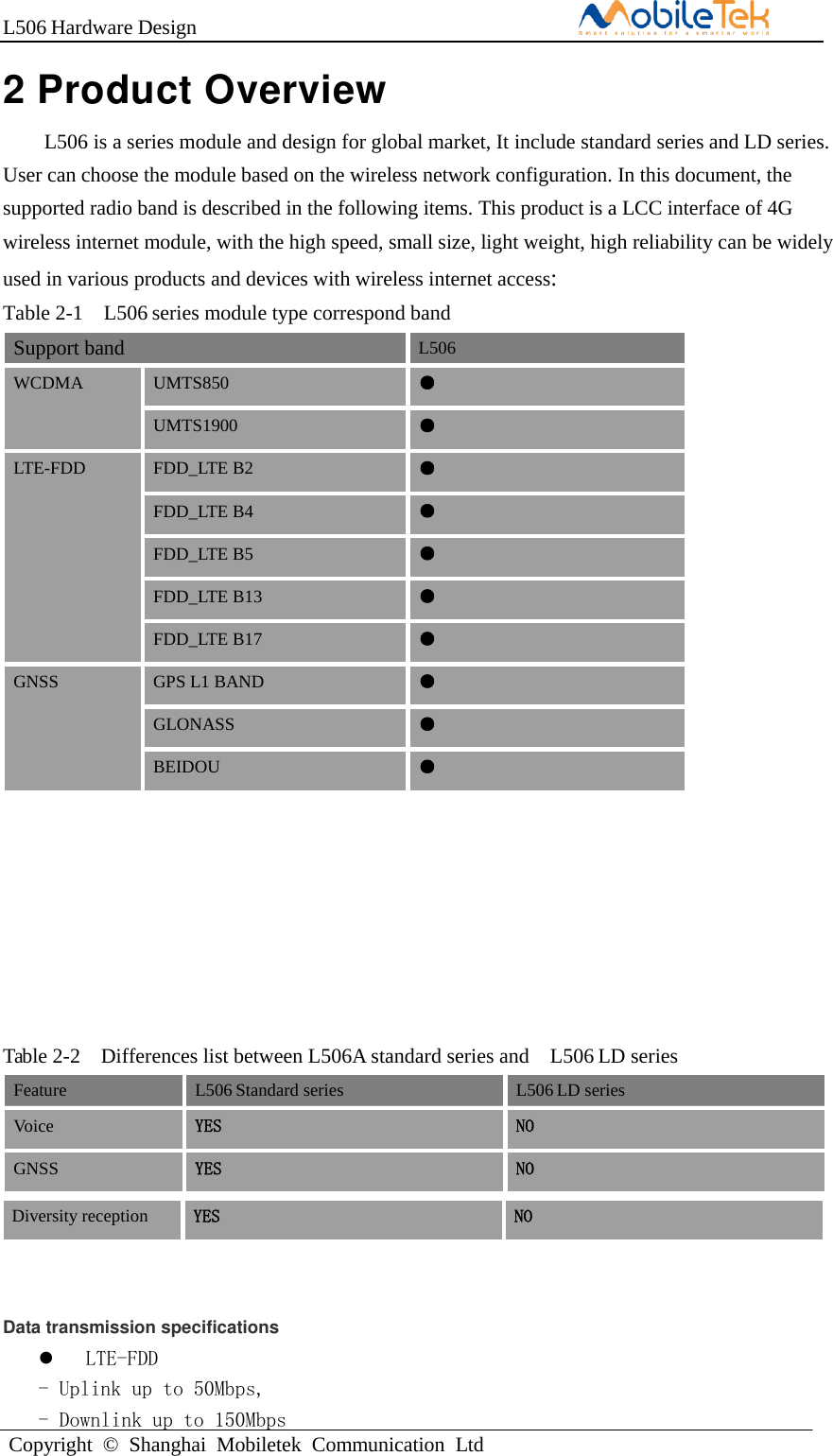
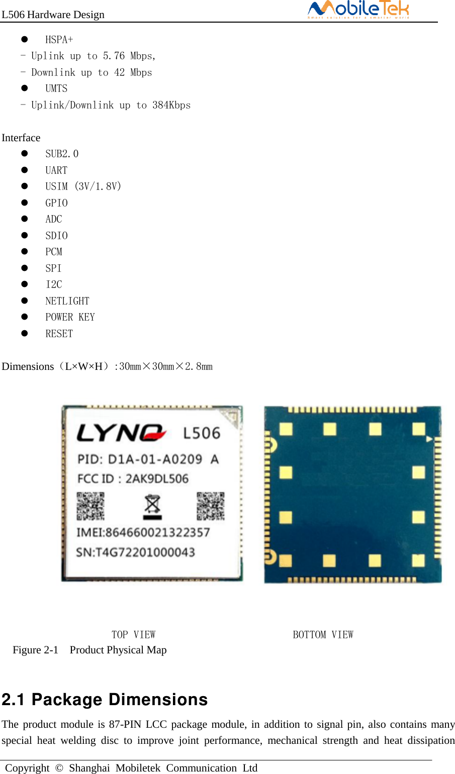
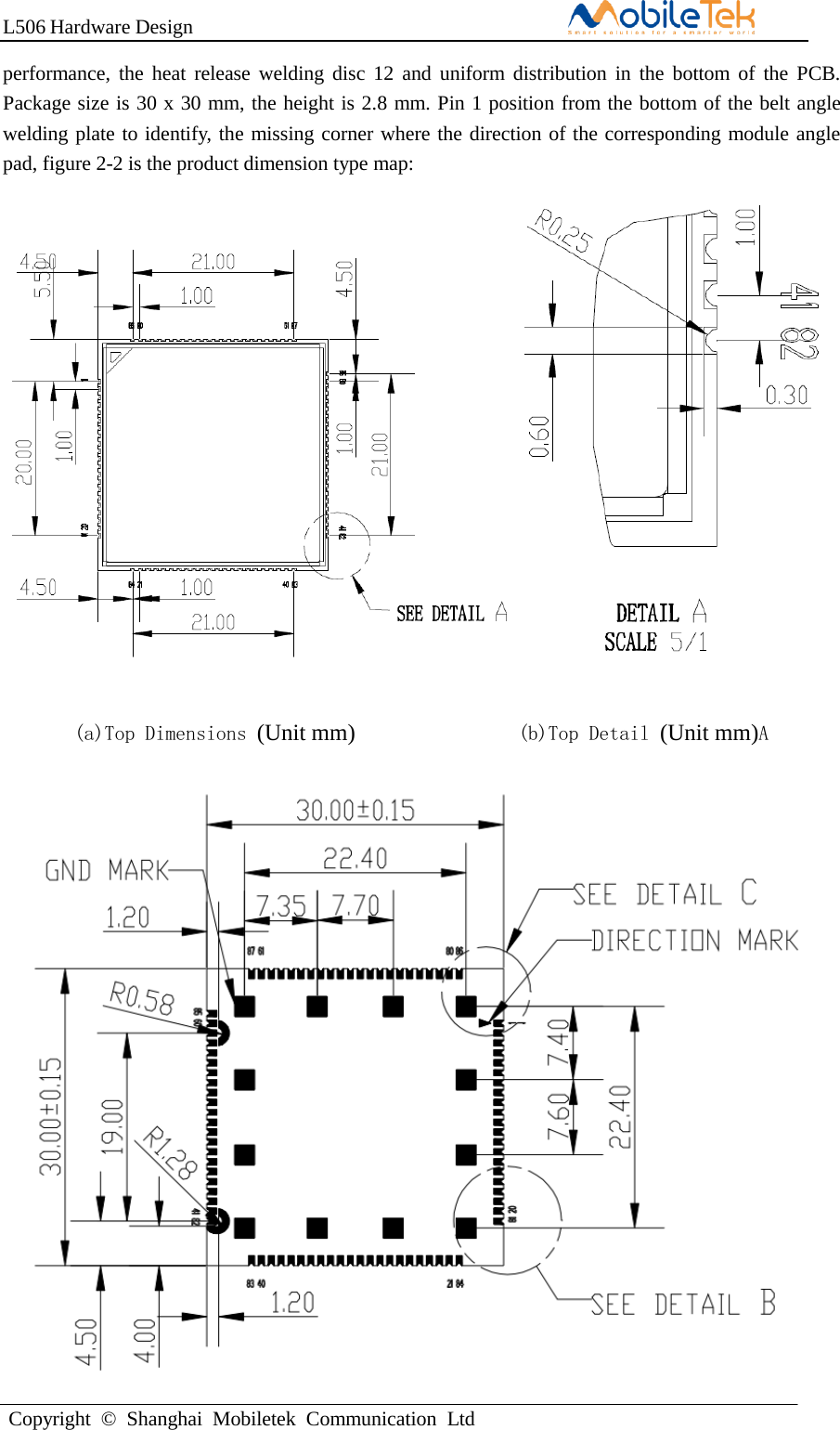
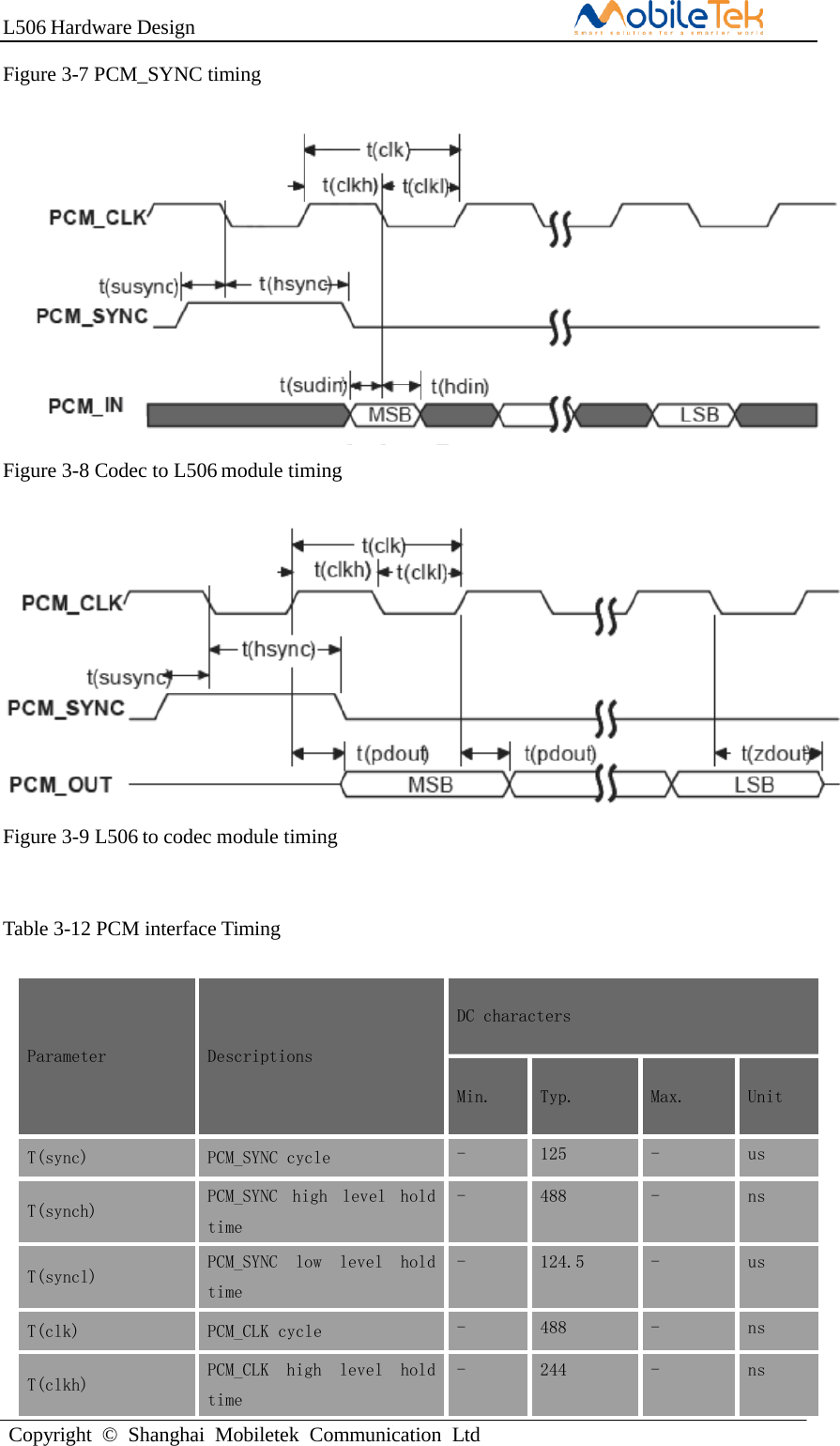
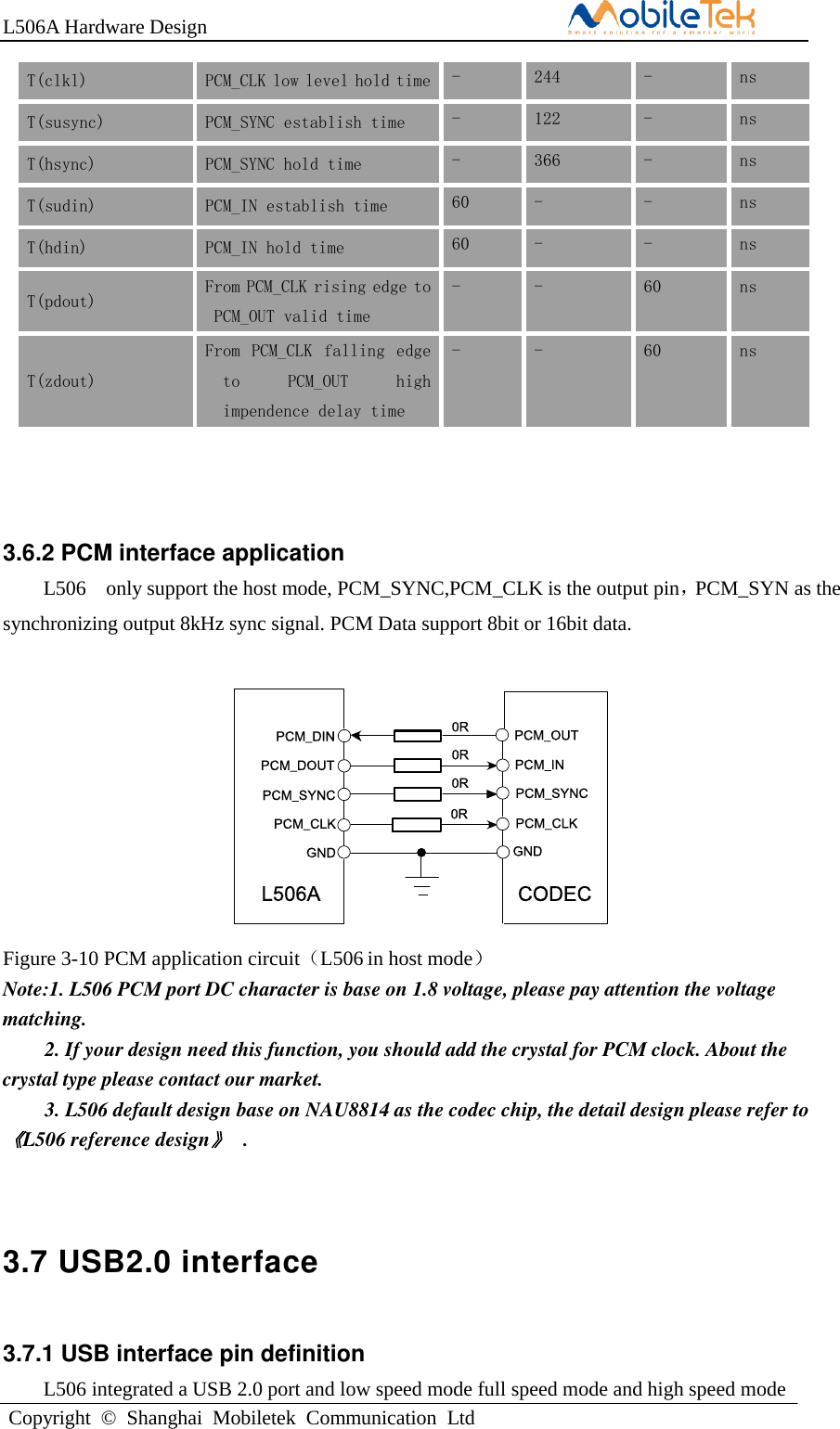
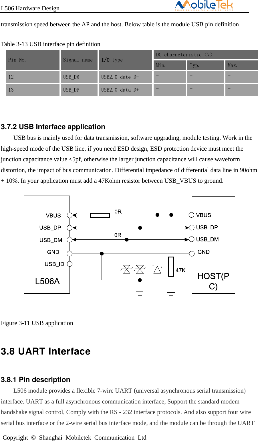
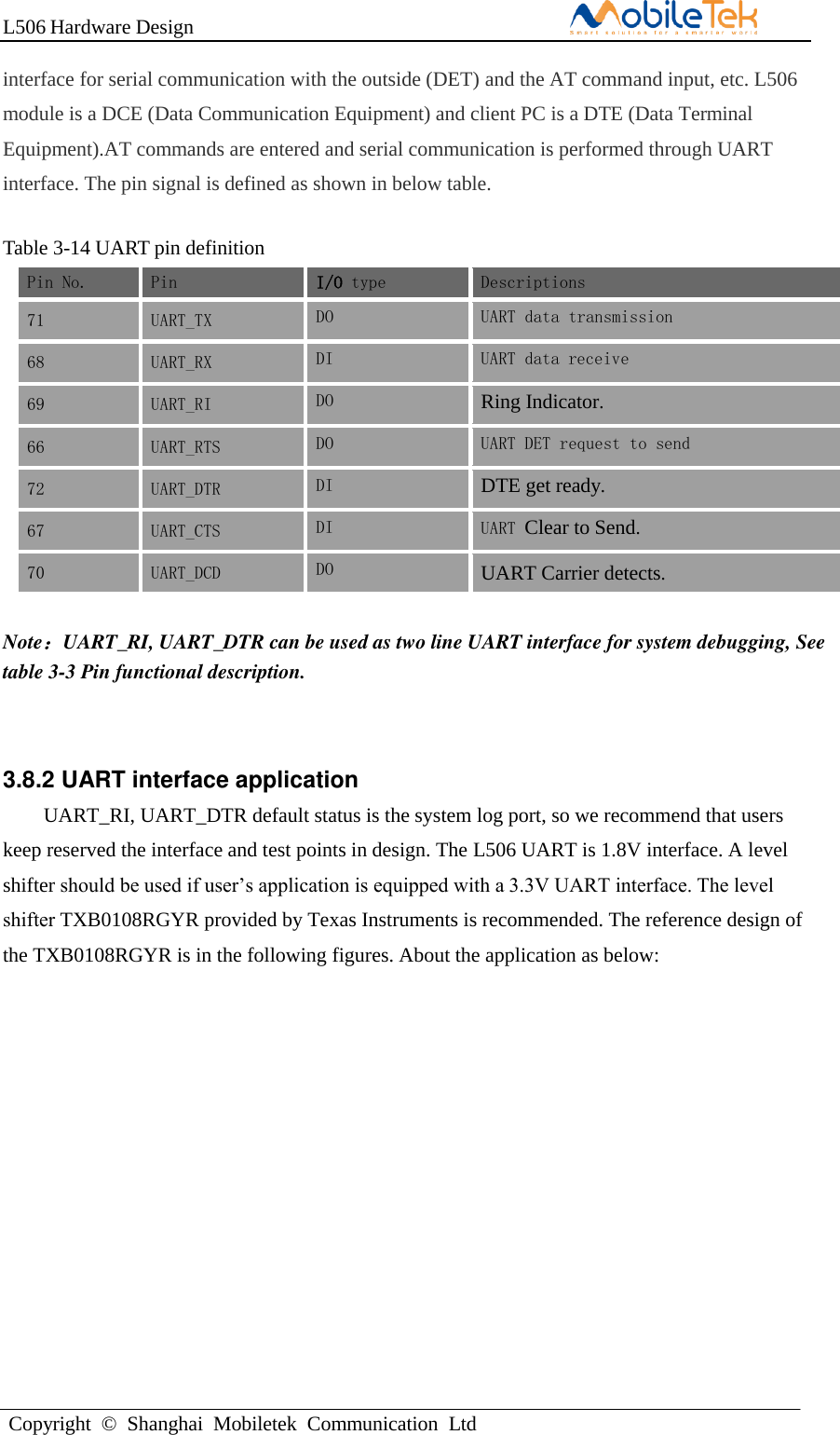
MobileTek Communication L506 LTE Module User Manual L506 hardware design
Shanghai MobileTek Communication Ltd. LTE Module L506 hardware design
UserManual.wiki
>
MobileTek Communication
>
L506 User Manual
User Manual
Navigation menu
Upload a User Manual
Namespaces
Wiki Guide
HTML
PDF
Info
Views
User Manual
Discussion / Help
Navigation
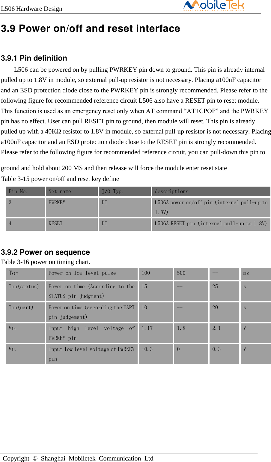
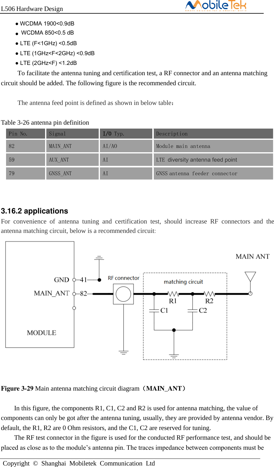
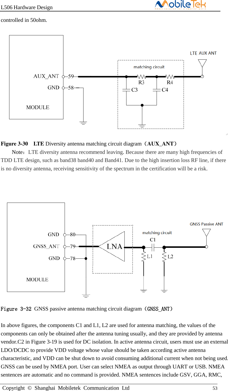
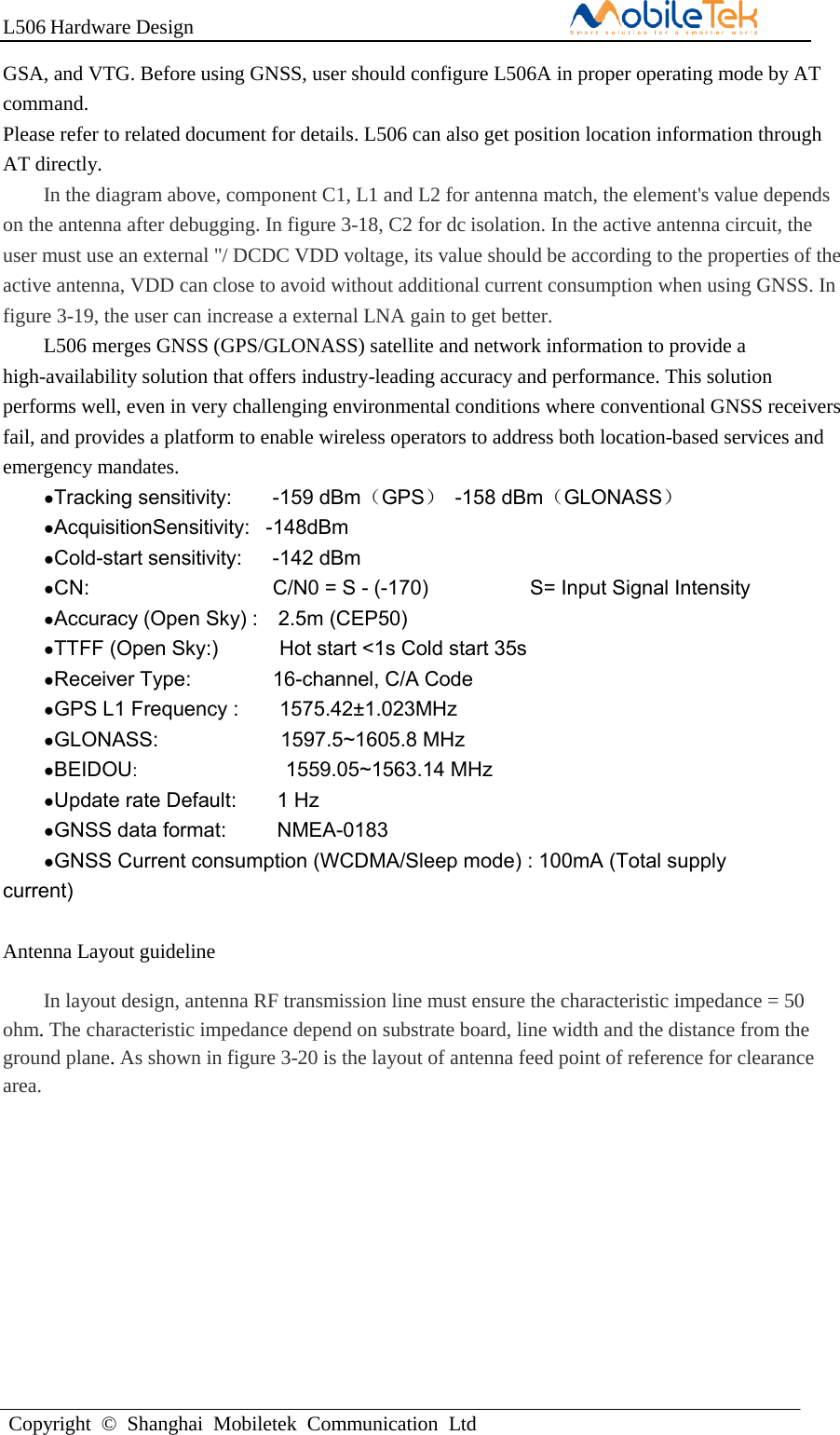
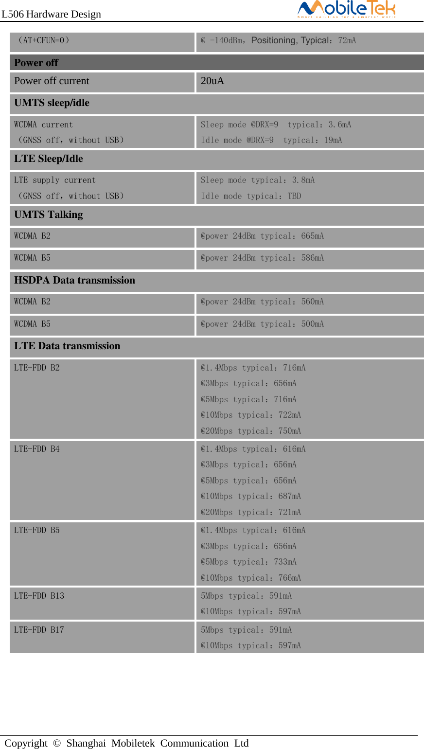
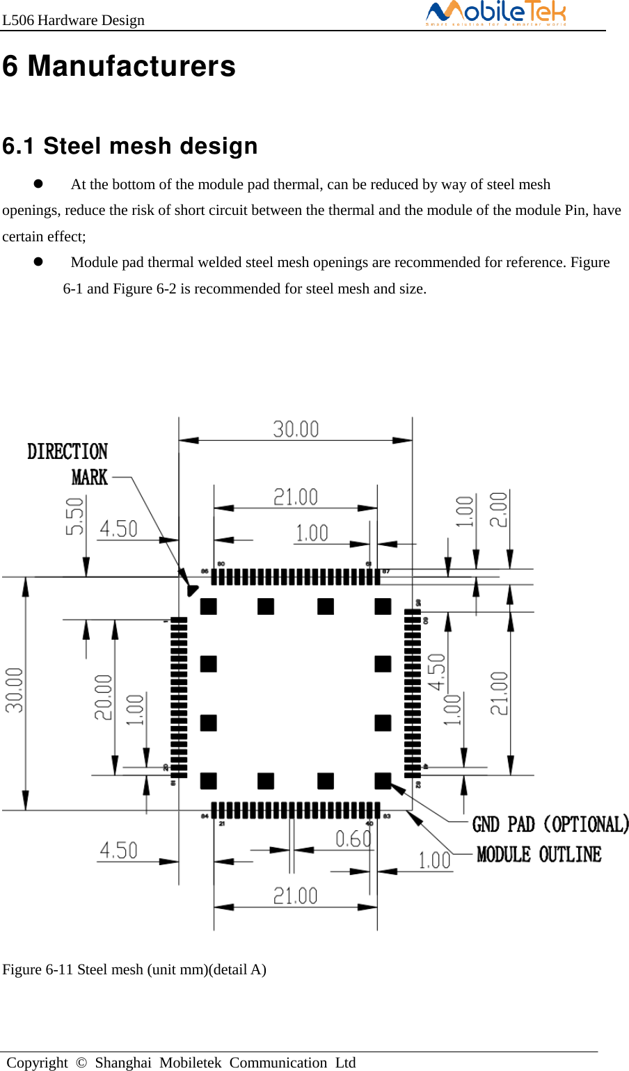
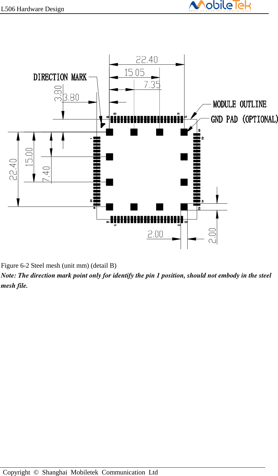
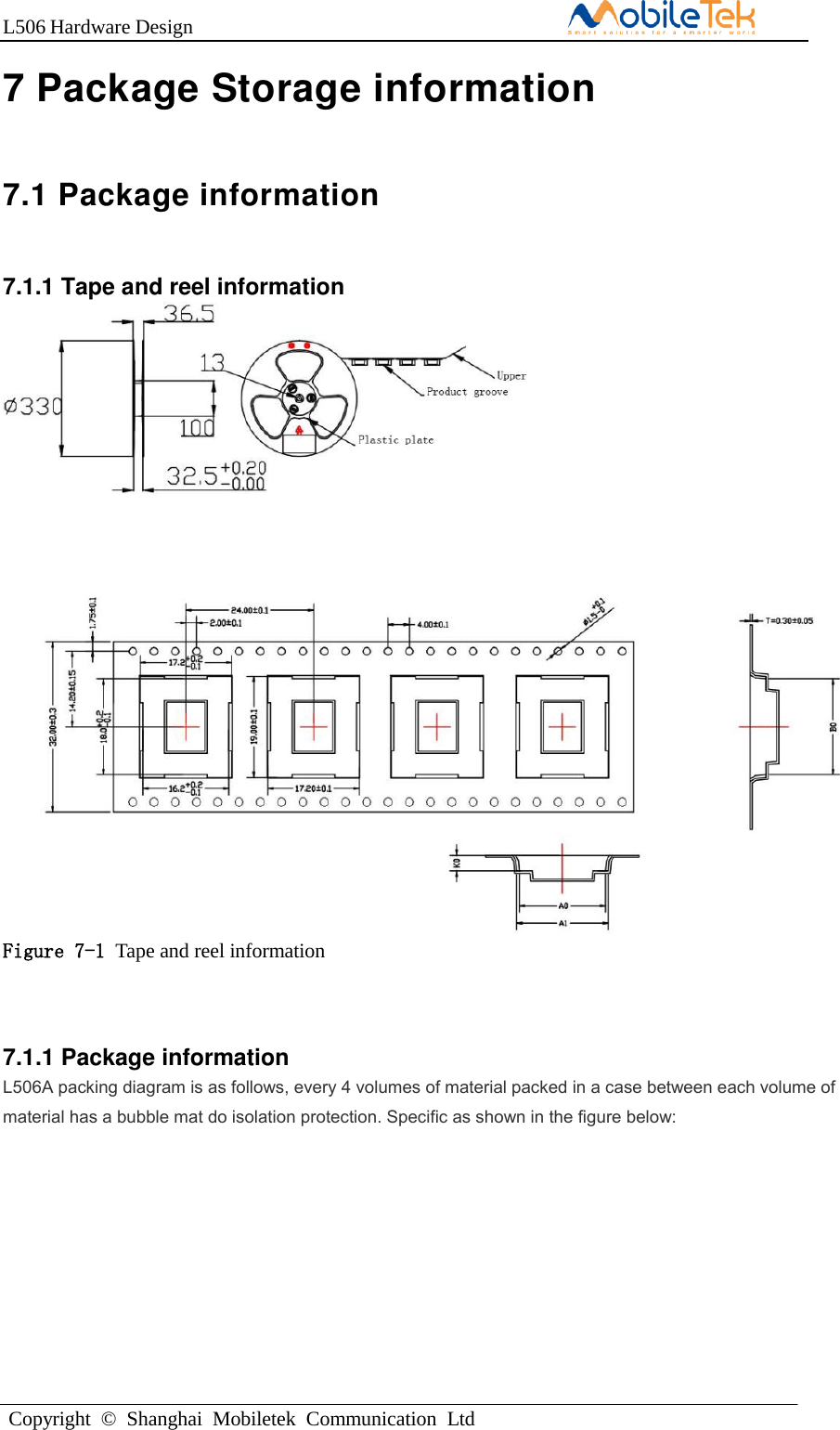
![L506A Hardware DesignCopyright © Shanghai Mobiletek Communication LtdFigures 3-17 Power on Timing sequence Note: the STATUS pin can be used to identify whether has been power on, when the module has access to electricity and initialization is completed, the STATUS output high level, or has maintained low level. 3.9.3 Power off sequence The following methods can be used to power down. These procedures will make module disconnect from the network and allow the software to enter a safe state, and then save data before completely powering the module off. ●Method 1: Power off L506A by pulling the PWRKEY pin down●Method 2: Power off L506A by AT command “AT+CPOF”●Method 3: over-voltage or under-voltage automatic power down.●Method 4: over-temperature or under-temperature automatic power down.Note: 1. About the AT command “AT+CPOF” detail please refer document [1]. 2. Over-voltage or under-voltage may cause automatic power down.3. Over-temperature or under-temperature may cause automatic power down.Table 3-17 Power off timing chart. Toff The time of active low level pulse on PWRKEY pin to power off module 2.5 -- -- s Toff(status) The time from power-off issue to STATUS pin output low level (indicating power off) 6 -- -- s Toff(uart) The time from power-off issue to UART port off 6 -- -- s Toff-on The buffer time from power-off issue to power-on issue 0 -- -- V VIH Input high level voltage of PWRKEY pin 1.17 1.8 2.1 V VIL Input low level voltage of PWRKEY -0.3 0 0.3 V](https://usermanual.wiki/MobileTek-Communication/L506/User-Guide-3601058-Page-37.png)
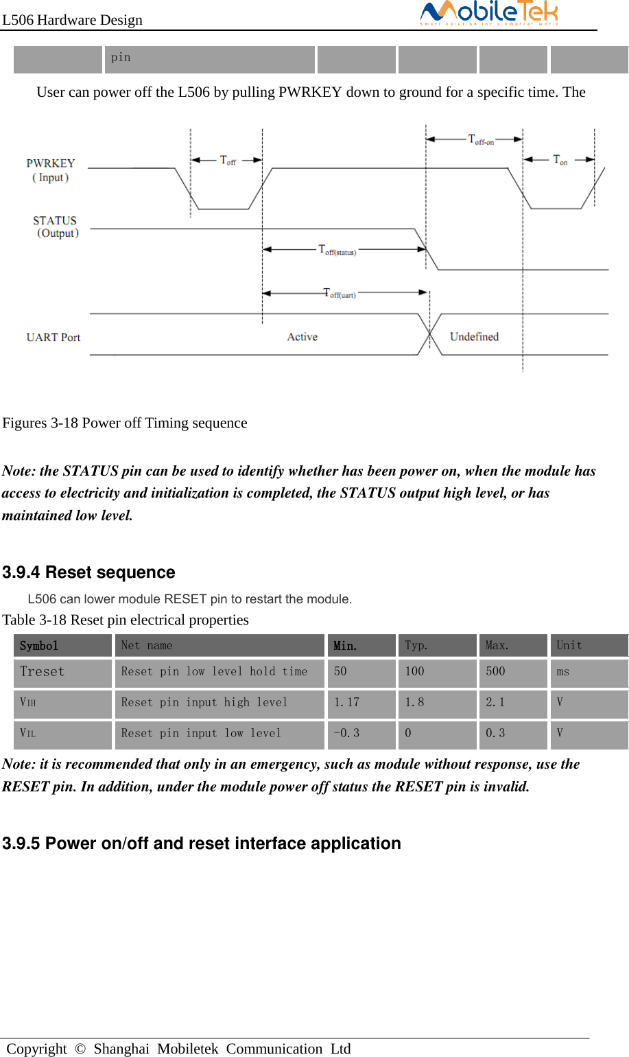
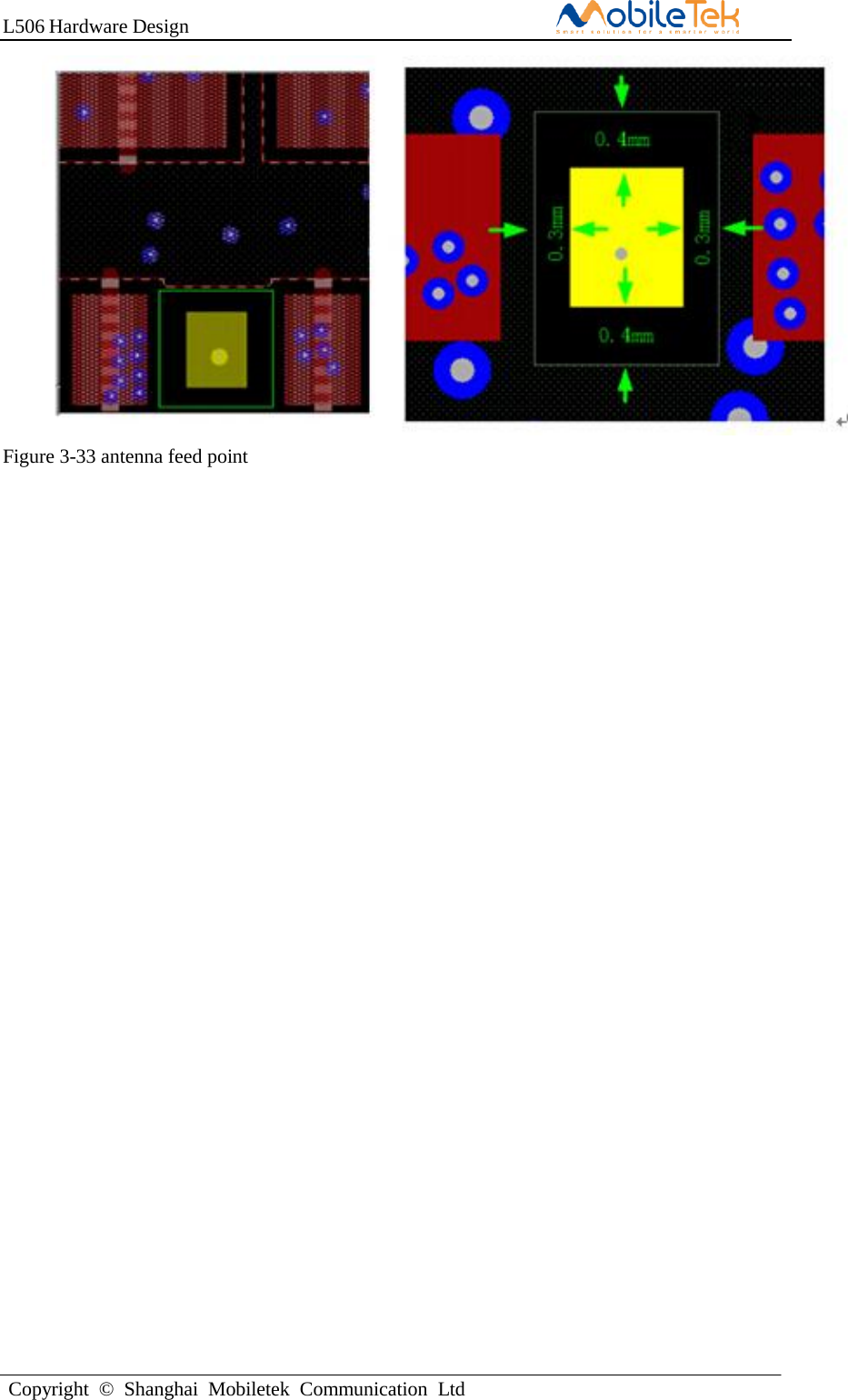
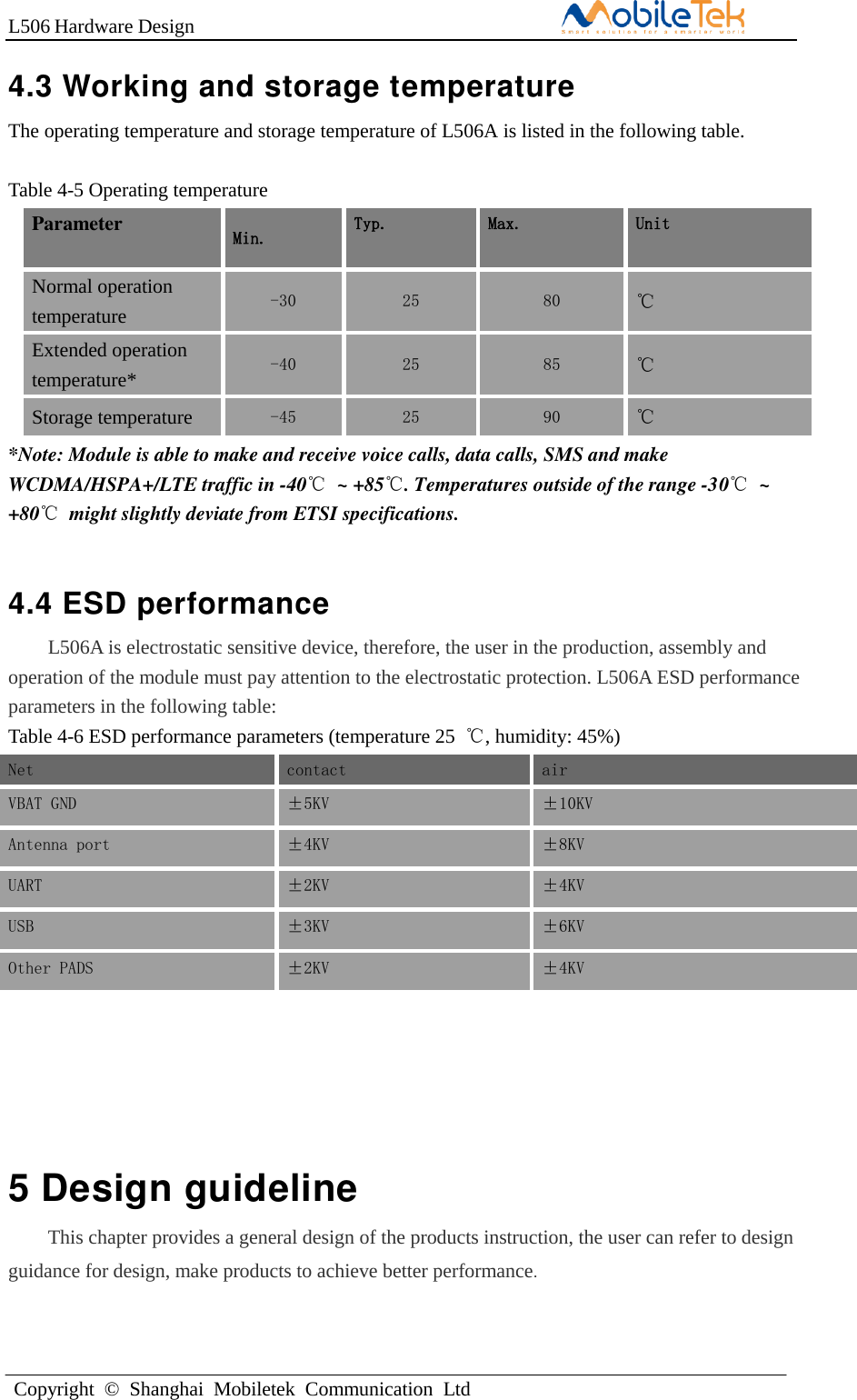
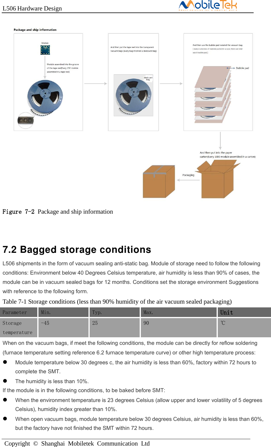
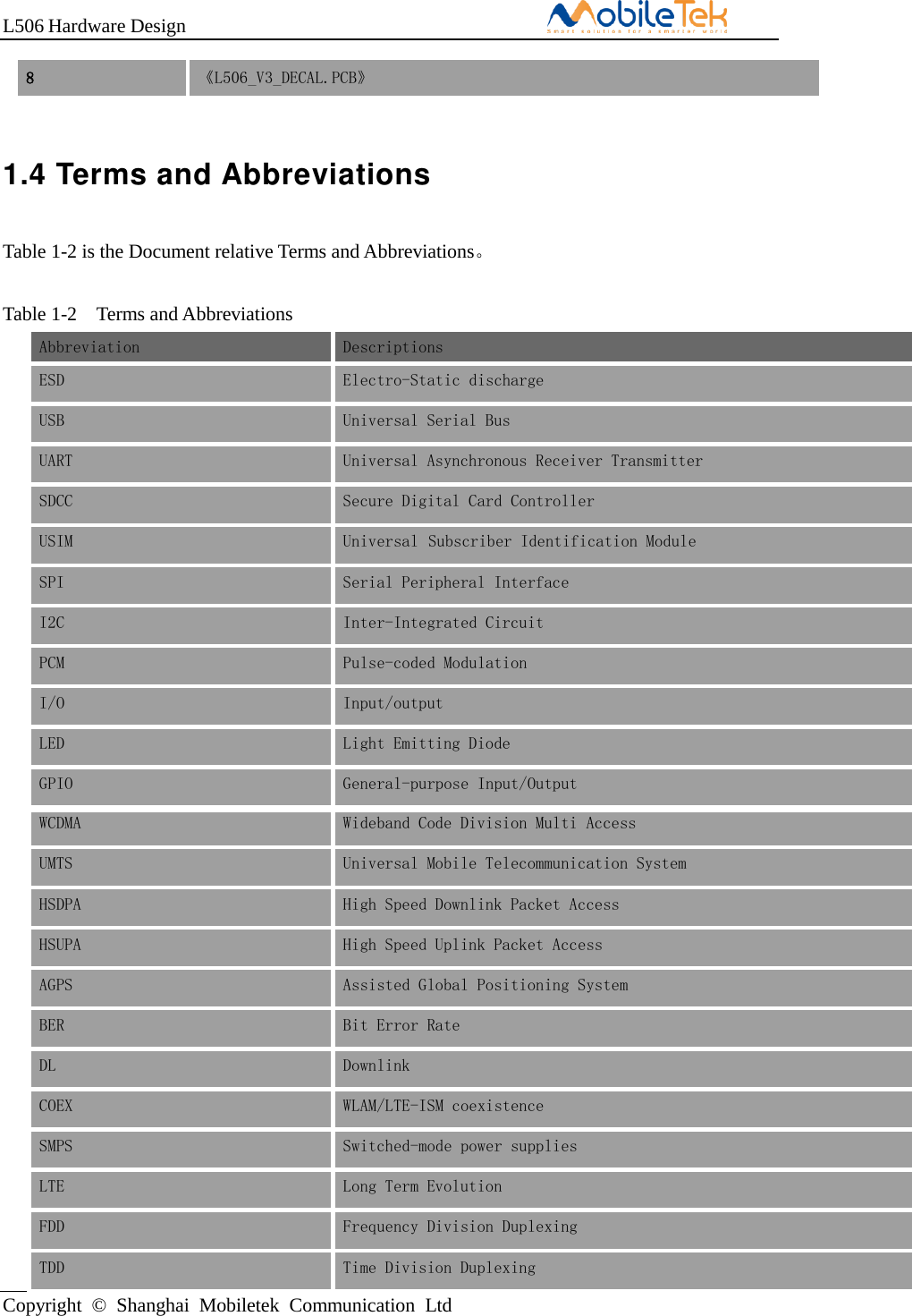
![L506 Hardware DesignCopyright © Shanghai Mobiletek Communication LtdInput voltage range 0.3 -- VBAT V Input resistance 1 -- -- MΩ Note: 1. use "AT + CADC" and "AT + CADC2" can read ADC1 and ADC2 voltage on the pin. More information please refer to the document [1]. 2. The need for special software version to support access to the ADC.3.15 I2C interface3.15.1 I2C pin definition I2C is used to communicate with peripheral equipment and can be operated as either a transmitter or receiver, depending on the device function. Both SDA and SCL are bidirectional lines connected with I2C interface. Its operation voltage is 1.8V. High speed mode transmission rate can reach 400 KBPS, Because L506 have internal pulled up to the I2C interface, so in your design needn’t pull up. Figure 3-15 is the reference design: Figure 3-28 I2C reference design Note: 1. L506 I2C only support host mode. 2. Only special software version support inquire the I2C.3.16 Antenna interface3.16.1 RF signal PCB layout guideL506 provides RF antenna interface. Customer’s antenna should be located in the host board and connected to module’s antenna pad through micro-strip line or other types of RF trace and the trace impedance must be controlled in 50Ω. we recommends that the total insertion loss between the antenna pad and antenna should meet the following requirements: Copyright © Shanghai Mobiletek Communication Ltd 50 3.14 Analog and Digital conversion (ADC) interfaceL506 integrated two analog-to-digital conversion interface, specific parameters are as follows: Table 3-25 ADC1, ADC2 characters characters Min. Typ. Max. Unit ADC resolution -- 15 -- Bits Transfer time -- 442 -- ms](https://usermanual.wiki/MobileTek-Communication/L506/User-Guide-3601058-Page-46.png)