MobileTek Communication L506 LTE Module User Manual L506 hardware design
Shanghai MobileTek Communication Ltd. LTE Module L506 hardware design
User Manual

/$+DUGZDUH'HVLJQ
&RS\ULJKW 6KDQJKDL 0RELOHWHN &RPPXQLFDWLRQ /WG
/+DUGZDUH'HVLJQ
LTE Module Series
Version: V1.0
Date: 2016-09-13
Shanghai Mobiletek Communication Ltd

L506 Hardware Design
Copyright © Shanghai Mobiletek Communication Ltd
Notice
Some features of the product and its accessories described herein rely on the software installed,
capacities and settings of local network, and therefore may not be activated or may be limited by local
network operators or network service providers.
Thus, the descriptions herein may not exactly match the product or its accessories which you purchase.
Shanghai Mobiletek Communication Ltd reserves the right to change or modify any information or
specifications contained in this manual without prior notice and without any liability.
Copyright
This document contains proprietary technical information which is the property of Shanghai Mobiletek
Communication Ltd. copying of this document and giving it to others and the using or communication
of the contents thereof, are forbidden without express authority. Offenders are liable to the payment of
damages. All rights reserved in the event of grant of patent or the registration of a utility model or
design. All specification supplied herein are subject to change without notice at any time.
DISCLAIMER
ALL CONTENTS OF THIS MANUAL ARE PROVIDED “AS IS”. EXCEPT AS REQUIRED BY
APPLICABLE LAWS, NO WARRANTIES OF ANY KIND, EITHER EXPRESS OR IMPLIED,
INCLUDING BUT NOT LIMITED TO, THE IMPLIED WARRANTIES OF MERCHANTABILITY
AND FITNESS FOR A PARTICULAR PURPOSE, ARE MADE IN RELATION TO THE
ACCURACY, RELIABILITY OR CONTENTS OF THIS MANUAL.
TO THE MAXIMUM EXTENT PERMITTED BY APPLICABLE LAW, IN NO EVENT SHALL
SHANGHAI MOBILETEK COMMUNICATION LTD BE LIABLE FOR ANY SPECIAL,
INCIDENTAL, INDIRECT, OR CONSEQUENTIAL DAMAGES, OR LOSS OF PROFITS,
BUSINESS, REVENUE, DATA, GOODWILL SAVINGS OR ANTICIPATED SAVINGS
REGARDLESS OF WHETHER SUCH LOSSES ARE FORSEEABLE OR NOT.

L506 Hardware Design
Copyright © Shanghai Mobiletek Communication Ltd
Version History
Date
Version
Description of change
Author
2016-09-13
V1.0
Initial

L506 Hardware Design
Copyright © Shanghai Mobiletek Communication Ltd
1 About this document
1.1Applicable scope
This document describes the L506 series 4G LTE LCC Module (hereinafter referred to as L506),
the basic specifications, product electrical characteristics, design guidance and hardware interface
development guidance. Users need to follow this documentation requirements and guidance for
design.
This document applies only to L506 products in the application development.
1.2 Writing purpose
This document provides the design and development basis for the product users. By reading this
document, users can have a whole understanding of the product, the technical parameters of the
product have a clear understanding, and can be used in this document to complete the development
of Internet access functions.
This hardware development document not only provides the product functional features and
technical parameters, but also provides product reliability testing and related testing standards,
business functions to achieve process, RF performance indicators and user circuit design guidance.
1.3 Support and reference documents list
In addition to the hardware development documentation, we also provide a guide to the
development board based on this product manual and software development instruction manual, 1-1 is
supported as a list.
Table 1-1 support document list
No.
Documents
1
《L506 AT Command User Guide》
2
《L506_SPEC.docx》
3
《L506 EVB User Manual》
4
《L506 Schematic checklist》
5
《L506 Layout checklist》
6
《L506_Reference Design_V3.pdf》
7
《L506_V1_DECAL.sch》
L506 Hardware Design
Copyright © Shanghai Mobiletek Communication Ltd
8
《L506_V3_DECAL.PCB》
1.4 Terms and Abbreviations
Table 1-2 is the Document relative Terms and Abbreviations。
Table 1-2 Terms and Abbreviations
Abbreviation
Descriptions
ESD
Electro-Static discharge
USB
Universal Serial Bus
UART
Universal Asynchronous Receiver Transmitter
SDCC
Secure Digital Card Controller
USIM
Universal Subscriber Identification Module
SPI
Serial Peripheral Interface
I2C
Inter-Integrated Circuit
PCM
Pulse-coded Modulation
I/O
Input/output
LED
Light Emitting Diode
GPIO
General-purpose Input/Output
WCDMA Wideband Code Division Multi Access
UMTS Universal Mobile Telecommunication System
HSDPA High Speed Downlink Packet Access
HSUPA High Speed Uplink Packet Access
AGPS Assisted Global Positioning System
BER Bit Error Rate
DL Downlink
COEX WLAM/LTE-ISM coexistence
SMPS Switched-mode power supplies
LTE Long Term Evolution
FDD Frequency Division Duplexing
TDD Time Division Duplexing

L506 Hardware Design
Copyright © Shanghai Mobiletek Communication Ltd
DPCH
Dedicated Physical Channel
DPCH_Ec
Average energy per PN chip for DPCH. DPCH
L506 Hardware Design
Copyright © Shanghai Mobiletek Communication Ltd
2 Product Overview
L506 is a series module and design for global market, It include standard series and LD series.
User can choose the module based on the wireless network configuration. In this document, the
supported radio band is described in the following items. This product is a LCC interface of 4G
wireless internet module, with the high speed, small size, light weight, high reliability can be widely
used in various products and devices with wireless internet access:
Table 2-1 L506 series module type correspond band
Support band
L506
WCDMA
UMTS850
●
UMTS1900
●
LTE-FDD
FDD_LTE B2
●
FDD_LTE B4
●
FDD_LTE B5
●
FDD_LTE B13
●
FDD_LTE B17
●
GNSS
GPS L1 BAND
●
GLONASS
●
BEIDOU
●
Table 2-2 Differences list between L506A standard series and L506 LD series
Feature
L506 Standard series L506 LD series
Voice
YES
NO
GNSS
YES
NO
Diversity reception YES NO
Data transmission specifications
LTE-FDD
- Uplink up to 50Mbps,
- Downlink up to 150Mbps
L506 Hardware Design
Copyright © Shanghai Mobiletek Communication Ltd
HSPA+
- Uplink up to 5.76 Mbps,
- Downlink up to 42 Mbps
UMTS
- Uplink/Downlink up to 384Kbps
Interface
SUB2.0
UART
USIM (3V/1.8V)
GPIO
ADC
SDIO
PCM
SPI
I2C
NETLIGHT
POWER KEY
RESET
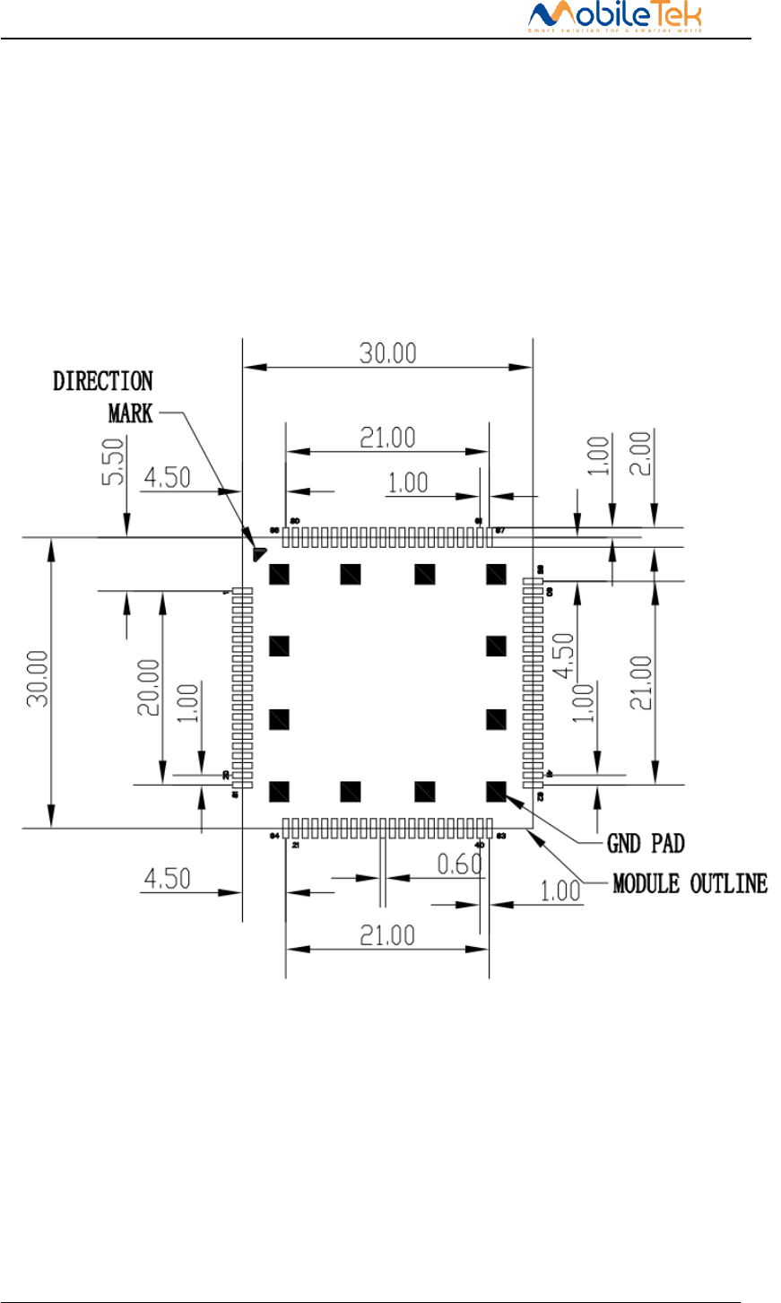
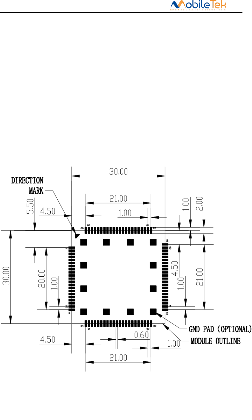
Dimensions(L×W×H):30mm×30mm×2.8mm
TOP VIEW BOTTOM VIEW
Figure 2-1 Product Physical Map
2.1 Package Dimensions
The product module is 87-PIN LCC package module, in addition to signal pin, also contains many
special heat welding disc to improve joint performance, mechanical strength and heat dissipation
L506 Hardware Design
Copyright © Shanghai Mobiletek Communication Ltd
performance, the heat release welding disc 12 and uniform distribution in the bottom of the PCB.
Package size is 30 x 30 mm, the height is 2.8 mm. Pin 1 position from the bottom of the belt angle
welding plate to identify, the missing corner where the direction of the corresponding module angle
pad, figure 2-2 is the product dimension type map:
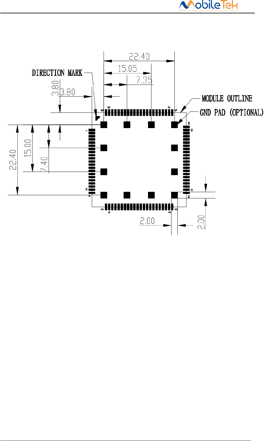
(a)Top Dimensions (Unit mm) (b)Top Detail (Unit mm)A
L506 Hardware Design
Copyright © Shanghai Mobiletek Communication Ltd
(c)Bottom Dimensions (Unit mm)
Note: antenna feed point in actual use of the customers don't need (PCB assembly, the stencil
file).
(d)Bottom Detail B (Unit mm)
L506 Hardware Design
Copyright © Shanghai Mobiletek Communication Ltd
(e)Bottom Detail C (Unit mm)
L506 Hardware Design
Copyright © Shanghai Mobiletek Communication Ltd
(e)Side view Dimensions(Unit mm)
Figure 2-2 Module Dimensions
2.2 Product Function Outline
2.2.1 Hardware Diagram
This product mainly includes the following signal group:USB Interface signal、USIM card
Interface signal、I2C Interface signal、UART Interface signal、PCM Interface signal、UART
Interface signal、SPI interface、Module startup、Module control signal、Power supply and ground.
L506 Hardware Design
Copyright © Shanghai Mobiletek Communication Ltd
2.2.2 Radio frequency function
RF Function Overview:
Five-Band FDD-LTE B2/B4/B5/B13/B17
Dual-Band UMTS/HSDPA/HSPA+ B2/B5
GPS/BEIDOU/GLONASS
The operating frequency range of the transmitter is shown in table 2-2.
Table 2-3 RF frequency band
Working band Upstream band(Uplink) Downlink frequency(Downlink)
WCDMA B5 824 MHz~849 MHz 869 MHz~894 MHz
WCDMA B2 1850 MHz — 1910 MHz 1930 MHz — 1990MHz
FDD_LTE B2 1850 MHz — 1910 MHz 1930 MHz — 1990MHz
FDD_LTE B4 1710 MHz~1755 MHz 2110 MHz~2155 MHz
FDD_LTE B5 824 MHz~849 MHz 869 MHz~894 MHz
FDD_LTE B13 777 MHz~787 MHz 746 MHz~756 MHz
FDD_LTE B17 704 MHz~716 MHz 734 MHz~746 MHz
GPS L1 BAND -- 1574.4 ~1576.44 MHz
GLONASS -- 1598 ~1606 MHz
BEIDOU B1 -- 1559.05 ~1563.14 MHz
L506 Hardware Design
Copyright © Shanghai Mobiletek Communication Ltd
Table 2-4 Conducted transmission power
Working Band Max Power Min Power
WCDMA B5 22.5dBm +/-1dB <-50dBm
WCDMA B2 23dBm +/-1dB <-50dBm
FDD_LTE B2 22dBm +/-1dB <-40dBm
FDD_LTE B4 22dBm +/-1dB <-40dBm
FDD_LTE B5 22dBm +/-1dB <-40dBm
FDD_LTE B13 21dBm +/-1dB <-40dBm
FDD_LTE B17 21dBm +/-1dB <-40dBm
Table 2-5 Conducted receive sensitivity
Working Band Receive sensitivity(Typical) Receive sensitivity(MAX)
WCDMA B2 < -108dBm 3GPP
WCDMA B5< -109dBm 3GPP
Table 2-6 Reference sensitivity (QPSK)
Channel bandwidth
E-UTRA Band 1.4 MHz 3 MHz 5 MHz 10 MHz 15 MHz 20 MHz Duplex Mode
2 -102.2 -99.7 -100 -97.2 -96.2 -95 FDD
4 -102.2 -99.7 -98 -95 -94.2 -93 FDD
5 -102.2 -99.7 -98 -95 -- -- FDD
13 -- -- -100.2 -97.2 -- -- FDD
17 -- -- -97 -94 -- -- FDD
YNQ
CON IDENTIAL
L506 Hardware Design
Copyright © Shanghai Mobiletek Communication Ltd
3 Interface Description
3.1 PIN Definition
3.1.1 Pin I/O parameter definition
The I/O parameter definition of the product is shown in table 3-1.
Table 3-1 I/O parameter definitions
Pin attribute symbol
Description
PI
Power input PIN
PO
Power output PIN
AI
Analog input
AIO
Analog signal input/output PIN
I/O
Digital signal input/output PIN
DI
Digital signal input
DO
Digital signal output
DOH
Digital output with high level
DOL
Digital output with low level
PD
Pull down
PU
Pull up
AO
Analog output
3.1.2 Pin Map
L506 haver different version, and the correspond pin definition show as special mark (* mark or
#mark) in the pin map. In the different hardware version the corresponding pin have differential
using, detail description show as below chart. All hardware interfaces which connect L506 to
customers’ application platform are through 87 pins pads (Metal half hole). Figure 3-1 is L506
outline diagram.
L506 Hardware Design
Copyright © Shanghai Mobiletek Communication Ltd
1
2
3
4
21
6
7
8
9
10
11
12
13
14
15
16
5
18
17
19
81
20
GND
GND
PWRKEY
RESET
GND
SD_CMD
SPI_CLK
SPI_MISO
SPI_MOSI
SPI_CS
GND
USB_VBUS
USB_DN
USB_DP
GND
VDD_1V8
USB_ID
USIM_DATA
USIM_RST
USIM_CLK
USIM_VDD
GND
85
60
59
58
56
55
54
53
52#
51
50#
49
48
47
46
45#
57
43
44
42*
82
41
BOOT_CFG0
GND
AUX_ANT
GND
GND
SDA
SCL
FLIGHTMODE
USIM_DET
GPIO_1/
WAKEUP_OUT
NETLIGHT
GPIO_2/
WAKEUP_IN
STATUS
SD1_DET
ADC1
ADC2
GPIO_0
VDD_EXT
GND
GND
MAIN_ANT
84#
COEX2
22
23
24
25
26
SD_DATA0
SD_DATA1
SD_DATA2
SD_DATA3
SD_CLK
28#
GPIO_3
27*
SDC1_DATA2
29*
30*
31*
32*
33*
SDC1_DATA1
SDC1_DATA3
SDC1_CMD
SDC1_DATA0
35*
P_CLK
34*VREG_L2_1V8
36*
37
38
39
40
SDC1_CLK
GND
VBAT
VBAT
GND
83
COEX1
61 GND
87
62
63
64
65
66
VBAT
VBAT
GND
GND
RTS
68 RXD
67 CTS
69#
70
71
72#
73
RI
DCD
TXD
DTR
PCM_OUT
75 PCM_SYNC
74 PCM_IN
76
77
78
79
80
PCM_CLK
GND
GND
GNSS_ANT
GND
86 COEX3
BOOT_CFG1
L506 LCC
TOP
Figure 3-1 Pin Map View (Top View)
Note: 1.
#flag pin in Figure 3-1 stand for multi-function pin. Detail description show as in
corresponding function description.
3.1.3 PIN Definition and function description
Table 3-2 Pin definition
Pin No.
Pin description
Pin No.
Pin description
1
GND
2
GND
3
PWRKEY
4
RESET
L506A Hardware Design
Copyright © Shanghai Mobiletek Communication Ltd
5
GND
6
SPI_CLK
7
SPI_MISO
8
SPI_MOSI
9
SPI_CS
10
GND
11
USB_VBUS
12
USB_DN
13
USB_DP
14
GND
15
VDD_1V8
16
USB_ID
17
USIM_DATA
18
USIM_RST
19
USIM_CLK
20
USIM_VDD
21
SD_CMD
22
SD_DATA0
23
SD_DATA1
24
SD_DATA2
25
SD_DATA3
26
SD_CLK
27*
SDC1_DATA2
28#
GPIO_3
29*
SDC1_DATA1
30*
31*
SDC1_DATA3
32*
SDC1_CMD
33*
SDC1_DATA0
34*
VREG_L2_1V8
35*
32K_SLEEP_CLK
36*
SDC1_CLK
37
GND
38
VBAT
39
VBAT
40
GND
41
GND
42*
43
GND
44
VDD_EXT
45#
GPIO_0
46
ADC2
47
ADC1
48
SD1_DET
49
STATUS
50#
GPIO_2/WAKEUP_IN
51
NETLIGHT
52#
GPIO_1/WAKEUP_OUT
53
USIM_DET
54
FLIGHTMODE
55
SCL
56
SDA
57
GND
58
GND
59
AUX_ANT
60
GND
61
GND
62
VBAT
63
VBAT
64
GND
65
GND
66
RTS
67
CTS
68
RXD
L506 Hardware Design
Copyright © Shanghai Mobiletek Communication Ltd
69#
RI
70
DCD
71
TXD
72#
DTR
73
PCM_OUT
74
PCM_IN
75
PCM_SYNC
76
PCM_CLK
77
GND
78
GND
79
GNSS_ANT
80
GND
81
GND
82
MAIN_ANT
83
COEX1
84
COEX2#
85
BOOT_CFG0
86
COEX3
87
BOOT_CFG1
Table 3-3 Pin Function Description
Power interface
Pin Name
Pin No.
I/O
Description
Content
VBAT
38,39,62,63
PI
Power supply voltage,
VBAT=3.4V~4.2V.
The power supply
for system Maximum
load current must
above 2A.
VDD_1V8
15
PO
Module LDO output
power ,1.8V output,
Max current 150mA,
For I/O, MCP, SLIC,
sensors.
If not use keep it
open.
VDD_EXT
44
PO
Module LDO output
power, 2.85V output,
Max current 300mA.
Only use for
external SD Card
VDD. If not use
keep it open.
GND
1,2,5,10,14,37
,40,41,43,57,5
8,60,61,64,65,
77,78,80,81
Ground.
System Control
Pin Name
Pin No.
I/O
Description
Content
PWRKEY
3
DI
System power on/off
input, active low.
RESET
4
DI
System reset input,
active low.
L506 Hardware Design
Copyright © Shanghai Mobiletek Communication Ltd
FLIGHTMODE
54
DI, PU
The input signal, used
to control the system
into flight mode, H:
flight mode; L: normal
mode
Pull UP to
VDD_1V8(PIN 15)
with 10K resistor
Module status(GPIO)
Pin Name
Pin No.
I/O
Description
Content
NETLIGHT
51
DO
Identify the system
network status.
STATUS
40
DO
Module status
identify: High level
power on, low level
power off.
SD interface
Pin Name Pin No. I/O Description Content
SD_CMD 21 DO SDIO command
Advice add the ESD
on you SD card
Slot. If not use
keep it open
SD_DATA0 22 I/O SDIO data
SD_DATA1 23 I/O SDIO data
SD_DATA2 24 I/O SDIO data
SD_DATA3 25 I/O SDIO data
SD_CLK 26 DO SDIO clock
SD_CARD_DET_N 48 DI,PU Input pin as SD card
detecting.
L506A have
internal pull up,
L506 Hardware Design
Copyright © Shanghai Mobiletek Communication Ltd
H: SD card is removed
L: SD card is inserted
so SD card slot
should choose
insert detect PIN
connect the
ground. If not use
keep it open
SIM interface
Pin Name
Pin No.
I/O
Description
Content
USIM_DETECT
53
DI,PU
Input pin as USIM card
detect pin.
H: USIM is removed
L: USIM is inserted
L506 have
internal pull up.
If not use keep
it open.
USIM_DATA
17
I/O
USIM Card data I/O,
which has been
pulled up with a 10KR
resistor to
USIM_VDD in module. Do
not pull
up or pull down in
users’ application
circuit.
All signals of
USIM
interface should
be protected with
ESD/EMC.
USIM_RESET
18
DO
USIM Reset
USIM_CLK
19
DO
USIM Clock
USIM_VDD
20
PO
USIM Card Power
output, output
Voltage depends on
USIM mode
automatically, and
one is
3.0V±10%, another is
1.8V±10%.
Current is less than
50mA.
PCM interface
Pin Name
Pin No.
I/O
Description
Content
PCM_CLK
76
DO
PCM data bit clock.
If not use keep it
open.
PCM_SYNC
75
DO
PCM data frame sync
signal.
PCM_IN
74
DI
PCM data input.
PCM_OUT
73
DO
PCM data output.
FULL UART/DEBUG PORT
Pin Name
Pin No.
I/O
Description
Content
L506 Hardware Design
Copyright © Shanghai Mobiletek Communication Ltd
RTS
66
DI
DET Request to send.
If not use keep it
open.
CTS
67
DO
Clear to Send.
If not use keep it
open.
RX
68
DI
Receive Data.
If not use keep it
open.
RI
69#
DO
Ring Indicator.
Multiplexed as
MDM_DBG_UART_TX.
If not use keep it
open. Recommend
reserved the test
point for debug
DCD
70
DO
Carrier detects.
If not use keep it
open
TXD
71
DO
Transmit Data.
If not use keep it
open.
DTR
72#
DI
DTE get ready.
Multiplexed as
MDM_DBG_UART_RX.
If not use keep it
open. Recommend
reserved the test
point for debug
I2C interface
Pin Name
Pin No.
I/O
Description
Content
I2C_SCL
55
DO
I2C clock output.
L506 internal
have pulled up to
1.8V
I2C_SDA
56
I/O
I2C data input/output.
GPIO
Pin Name
Pin No.
I/O
Description
Content
GPIO_2/WAKEUP_IN
50
I/O
Default: GPIO
Optional: Input pin as
wake/interrupt
signal to module from
host.
If not use keep it
open.
GPIO_1/WAKEUP_OU
T
52
DO
Default: GPIO
Optional: Output pin
as wake/interrupt
signal to host from
module.
GPIO_3
28
I/O
GPIO
GPIO_0
45
DO
Default: GPIO
L506 Hardware Design
Copyright © Shanghai Mobiletek Communication Ltd
Optional: output
control pin.
RF port
Pin Name
Pin No.
I/O
Description
Content
MAIN _ANT
82
AIO
Main Antenna
AUX_ANT
59
AI
diversity antenna
GNSS_ANT
79
AI
GPS antenna
Others
Pin Name
Pin No.
I/O
Description
Content
ADC1
47
AI
Analog conversion
digital input
interface1
If not use keep it
open.
ADC2
46
AI
Analog conversion
digital input
interface2
COEX1
83
I/O
RF synchronizing
LTE.
If not use keep it
open.
COEX3
86
I/O
COEX2
84#
I/O
Default: RF
synchronizing
Optional: Pull up to
1.8V (L506A PIN
15 VDD_1V8) with
10K resistor force
module in USB
download mode
Recommend placing
test points for
debug.
BOOT_CFG0
85
DI, PD
Pull up to 1.8V (L506A
PIN 15 VDD_1V8) with
10K resistor force
module in fastboot
mode
BOOT_CFG1
87
DI, PD
Pull up to 1.8V (L506A
PIN 15 VDD_1V8) with
10K resistor force
module in fastboot
mode
L506 Hardware Design
Copyright © Shanghai Mobiletek Communication Ltd
3.2 Operating condition
Table 3-4 module recommended operating condition
Parameter
Description
Min.
Typ.
Max.
Unit
VBAT
Main power supply for
the module
3.4
3.8
4.2
V
3.3 Digital I/O characteristics
Table 3-5 1.8V Digital I/O characteristics
Parameter
Description
Min.
Typ.
Max.
Unit
VIH
High level input voltage
0.7*VDD_PX
VDD_PX
VDD_PX+0.3
V
VIL
Low level input voltage
-0.3
0
0.2* VDD_PX
V
VOH
High level output voltage
VDD_PX-0.45
-
VDD_PX
V
VOL
Low level output voltage
0
0
0.45
V
IOH
High-level output current
(no pull down resistor)
-
2
-
mA
IOL
Low-level output current
(no pull up resistor)
-
-2
-
mA
IIH
Input high leakage
current (no
pull down resistor)
-
-
1
uA
IIL
Input low leakage current
(no pull up resistor)
-1
-
-
uA
*Note: 1. These parameters are for digital interface pins, such as SP, SDIO, GPIOs
(NETLIGHT,
FLIGHTMODE, STATUS, USIM_DET, SD1_DET), I2C, UART, PCM, COEXn, BOOT_CFGn.
2. L506A TF-card signal (SD_DATA0~SD_DATA3, SD_CLK, SD_CMD), USIM card signal
(USIM_CLK, USIM_DATA, USIM_RST) support dual-voltage (1.8V and 3.0V) mode, and the DC
character show in corresponding function block.
3.4 Power Interface
3.4.1 Power supply pin description
L506 Hardware Design
Copyright © Shanghai Mobiletek Communication Ltd
Table 3-6 DC Power Characteristics
Pin No.
Net Name
Description
DC Characteristic(V)
Min.
Typ.
Max.
38,39,62,63
VBAT
Power supply for
the module
3.4
3.8
4.2
1,2,5,10,14,37,40,
41,43,57,58,60,61,
64,65,77,78,80,81
GND
GND
-
-
-
44
VCC_EXT
Power supply for
external SD card
-
2.85
-
20
USIM_VDD
Power supply for
VDD SIM
-
1.8/3.0
-
15
VDD_1V8
LDO 1.8V output
-
1.8
-
88-99*
GND
Thermal and
welding fixed
plate
-
-
-
Note: Pin88~Pin99 (total12pin) is design for the thermal welding fixed plate.
3.4.2 Power supply requirements
There are four VBAT PIN power for the module, VBAT directly power supply for the module
baseband and PA, and operating rating is 3.4V~4.2V; In the weak network environment, the antenna
will be maximum power emission. The peak current of the module under the 3G mode may reach
the peak current of 1.8A. power supply to reach 2A, the average current to reach 0.9A above.
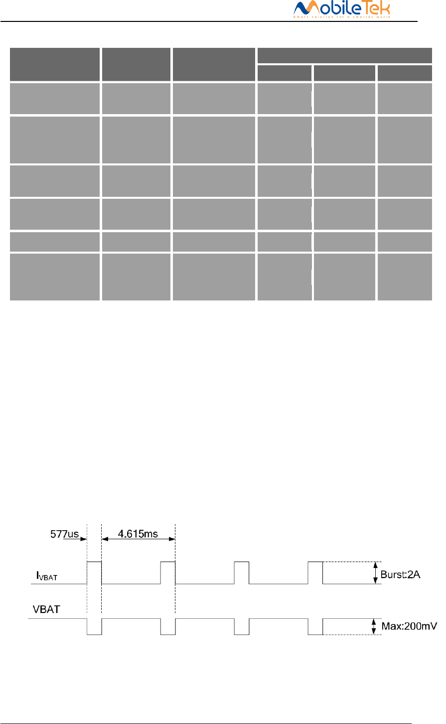
maximum peak current can reach 2A, So the max power supply current must more than 2 A. Figure
3-2 sign for instantaneous pulse diagram.
Figure 3-2 instantaneous pulse
L506 Hardware Design
Copyright © Shanghai Mobiletek Communication Ltd
Table 3-7 VBAT power supply interface characteristics
Symbol
Description
Min
Typ
Max
Unit
VBAT
Power supply
voltage
3.4
3.8
4.2
V
IVBAT(peak)
Power supply p
current
-
2*
-
A
IVBAT(average)
Power supply
average
current
1
1.5
-
A
IVBAT(power-off)
Power supply
current
in power off
mode
-
-
20
uA
IVBAT(power-save)
Power supply
current
in power save
mode(sleep
mode)
-
-
3
mA
3.4.3 Power Supply Design Guide
Make sure that the input voltage at the VBAT pin will never drop below 3.4V even during a
transmit burst when the current consumption rises up to more than 2A. If the power voltage drops
below 3.4V, the RF performance of module may be affected. Using large tantalum capacitors (above
300uF) will be the best way to reduce the voltage drops. If the power current cannot support up to 2A,
users must introduce larger capacitor (typical 1000uF) to storage electric power. For the consideration
of RF performance and system stability, some multi-layer ceramic chip (MLCC) capacitors (0.1/1uF)
need to be used for EMC because of their low ESR in high frequencies. Note that capacitors should be
put beside VBAT pins as close as possible. Also User should keep VBAT net wider than 2 mm to
minimize PCB trace impedance on circuit board. The following figure is the recommended circuit.
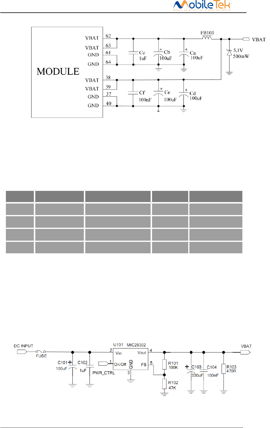
L506 Hardware Design
Copyright © Shanghai Mobiletek Communication Ltd
Figure 3-3 VBAT input application circuit
Note: The Cd, Ce, Cb, Cc and Cf are recommended being mounted for L506, but the Ca, Cb, Ce,
Cc and Cf for tune.
In addition, in order to get a stable power source, it is suggested to use a Zener diode of which
reverse Zener voltage is 5.1V and dissipation power is more than 500mW.
Table 3-8: Recommended Zener diode models
NO.
Manufacturer
Part Number
Power
Package
1
On semi
MMSZ5231BT1G
500mW
SOD123
2
Prisemi
PZ3D4V2H
500mW
SOD123
3
Vishay
MMSZ4689-V
500mW
SOD123
4
Crownpo
CDZ55C5V1SM
500mW
0805
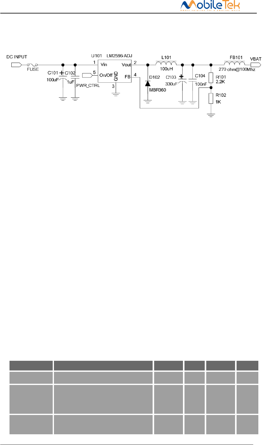
3.4.4 Recommended Power supply circuit
If the voltage difference is not big,We recommend DCDC or LDO is used for the power supply of the
module, make sure that the peak current of power components can rise up to more than 2A. The
following figure is the reference design of +5V input linear regulator power supply. The designed
output for the power supply is 3.8V.
Figure 3-4 Reference circuit of the LDO power supply
L506 Hardware Design
Copyright © Shanghai Mobiletek Communication Ltd
If there is a big difference between the input voltage and the desired output (VBAT) or better
efficiency is more important, a switching converter power supply will be preferable. The following
figure is the reference circuit.
Figure 3-5 Reference circuit of the DCDC power supply
Note: DCDC may deprave RF performance because of ripple current intrinsically.
3.4.5 Power Supply Layout guide
The layout of the power supply section and the related components is of vital importance in the
power module design. If processes this part layout is not good, will lead to various effects, such as bad
EMC, effective the emission spectrum and receiving sensitivity, etc. So the power supply part design
is very important, when you design this part you should notes below contents: 1. DC DC switch power
should place away from the antenna and other sensitivity circuit; 2. Consider the voltage drop and the
module current requirement, the layout line should better above 100mil. If conditions allow should add
a power shape plane.
3.5 USIM interface
3.5.1 Pin definition
The L506 integrated a ISO 7816-2 standard USIM port, and the module can automatic identify the
voltage demo according the USIM to allow the mobile equipment to attach to the network. Both 1.8V
and 3.0V SIM Cards are supported.
Table 3-9 USIM Electronic characteristic in 1.8V mode (USIM_VDD =1.8V)
Symbol
Parameter
Min.
Typ.
Max.
Unit
USIM_VDD
LDO power output
1.75
1.8
1.95
V
VIH
High-level input voltage
0.65·USI
M_VDD
-
USIM_V
DD +0.3
V
VIL
Low-level input voltage
-0.3
0
0.35·USI
M_VDD
V

L506 Hardware Design
Copyright © Shanghai Mobiletek Communication Ltd
VOH
High-level output voltage
USIM_V
DD -0.45
--
USIM_V
DD
V
VOL
Low-level output voltage
0
0
0.45
V
Table 3-10: USIM Electronic characteristic 3.0V mode (USIM_VDD =3.0V)
Symbol
Parameter
Min.
Typ.
Max.
Unit
USIM_VDD
LDO power output
2.75
3.0
3.05
V
VIH
High-level input voltage
0.65*USI
M_VDD
-
USIM_V
DD +0.3
V
VIL
Low-level input voltage
-0.3
0
0.25·USI
M_VDD
V
VOH
High-level output voltage
USIM_V
DD -0.45
-
USIM_V
DD
V
VOL
Low-level output voltage
0
0
0.45
V
3.5.2 Design Guide
USIM electronic characteristics as the table 3-8,3-9 show.
In order to meet the 3 GPP TS 51.010 1 protocol and EMC certification requirements. Suggest
USIM slot near the location of the module USIM card interface, to avoid running for too long, lead to
serious deformation of waveform and effect signal integrity, USIM_CLK and USIM_DATA signal
lines suggest ground protect. Between the USIM VCC & GND add a 1uF and a 33 pF capacitor in
parallel, Between the USIM_CLK& GND, USIM_RST& GND, USIM DATA& GND add a 33 pF
capacitor in parallel, for filter the RF signal interference.
3.5.3 USIM interface reference circuit
LY AL
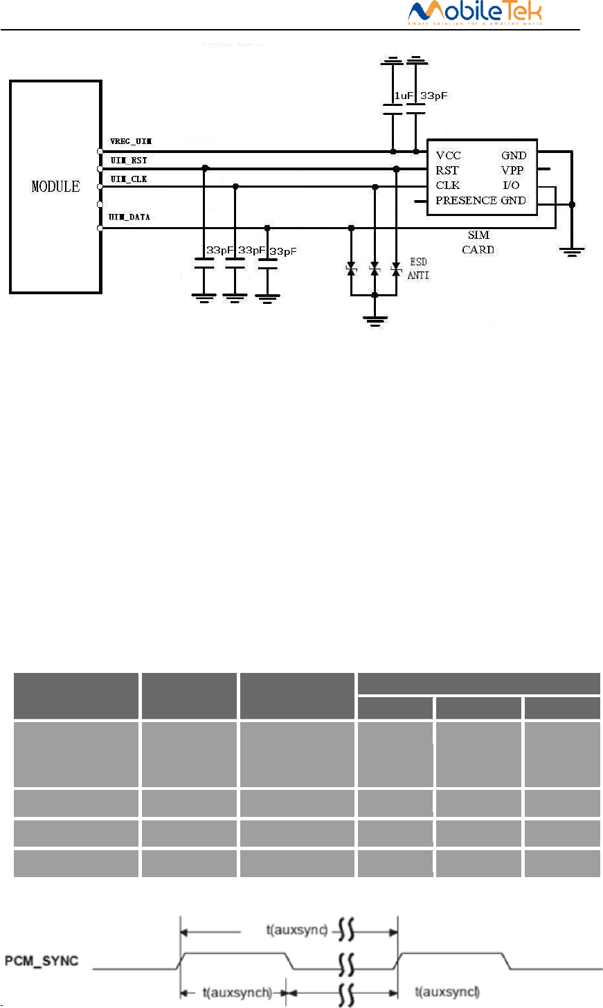
L506 Hardware Design
Copyright © Shanghai Mobiletek Communication Ltd
Figure 3-6 USIM Reference circuit
Note:USIM_DATA have added the pull-up resistance in the module design.
3.6 PCM interface
3.6.1 PCM interface definition
L506 provides hardware PCM interface for external codec. L506 PCM interface can be used in
short sync master mode only, and only supports 16 bits linear format:
Table 3-11 PCM interface definition
Pin No.
Signal name
I/O Type
DC Characteristics(V)
Min.
Typ.
Max.
75
PCM_SYNC
PCM
synchronizing
signal
-0.3
1.8
1.9
74
PCM_DIN
PCM data input
-0.3
1.8
1.9
73
PCM_DOUT
PCM Data output
-0.3
1.8
1.9
76
PCM_CLK
PCM Data clock
-0.3
1.8
1.9
L506 Hardware Design
Copyright © Shanghai Mobiletek Communication Ltd
Figure 3-7 PCM_SYNC timing
Figure 3-8 Codec to L506 module timing
Figure 3-9 L506 to codec module timing
Table 3-12 PCM interface Timing
Parameter
Descriptions
DC characters
Min.
Typ.
Max.
Unit
T(sync)
PCM_SYNC cycle
-
125
-
us
T(synch)
PCM_SYNC high level hold
time
-
488
-
ns
T(syncl)
PCM_SYNC low level hold
time
-
124.5
-
us
T(clk)
PCM_CLK cycle
-
488
-
ns
T(clkh)
PCM_CLK high level hold
time
-
244
-
ns
L506A Hardware Design
Copyright © Shanghai Mobiletek Communication Ltd
T(clkl)
PCM_CLK low level hold time
-
244
-
ns
T(susync)
PCM_SYNC establish time
-
122
-
ns
T(hsync)
PCM_SYNC hold time
-
366
-
ns
T(sudin)
PCM_IN establish time
60
-
-
ns
T(hdin)
PCM_IN hold time
60
-
-
ns
T(pdout)
From PCM_CLK rising edge to
PCM_OUT valid time
-
-
60
ns
T(zdout)
From PCM_CLK falling edge
to PCM_OUT high
impendence delay time
-
-
60
ns
3.6.2 PCM interface application
L506A only support the host mode, PCM_SYNC,PCM_CLK is the output pin,PCM_SYN as the
synchronizing output 8kHz sync signal. PCM Data support 8bit or 16bit data.
L506A CODEC
PCM_IN
PCM_SYNC
PCM_OUT
PCM_CLK
GND
GND
PCM_DIN
PCM_DOUT
PCM_SYNC
PCM_CLK
0R
0R
0R
0R
Figure 3-10 PCM application circuit(L506 in host mode)
Note:1. L506 PCM port DC character is base on 1.8 voltage, please pay attention the voltage
matching.
2. If your design need this function, you should add the crystal for PCM clock. About the
crystal type please contact our market.
3. L506 default design base on NAU8814 as the codec chip, the detail design please refer to
《
L506 reference design
》
.
3.7 USB2.0 interface
3.7.1 USB interface pin definition
L506 integrated a USB 2.0 port and low speed mode full speed mode and high speed mode
L506 Hardware Design
Copyright © Shanghai Mobiletek Communication Ltd
transmission speed between the AP and the host. Below table is the module USB pin definition
Table 3-13 USB interface pin definition
Pin No.
Signal name
I/O type
DC characteristic(V)
Min.
Typ.
Max.
12
USB_DM
USB2.0 date D-
-
-
-
13
USB_DP
USB2.0 data D+
-
-
-
3.7.2 USB Interface application
USB bus is mainly used for data transmission, software upgrading, module testing. Work in the
high-speed mode of the USB line, if you need ESD design, ESD protection device must meet the
junction capacitance value <5pf, otherwise the larger junction capacitance will cause waveform
distortion, the impact of bus communication. Differential impedance of differential data line in 90ohm
+ 10%. In your application must add a 47Kohm resistor between USB_VBUS to ground.
Figure 3-11 USB application
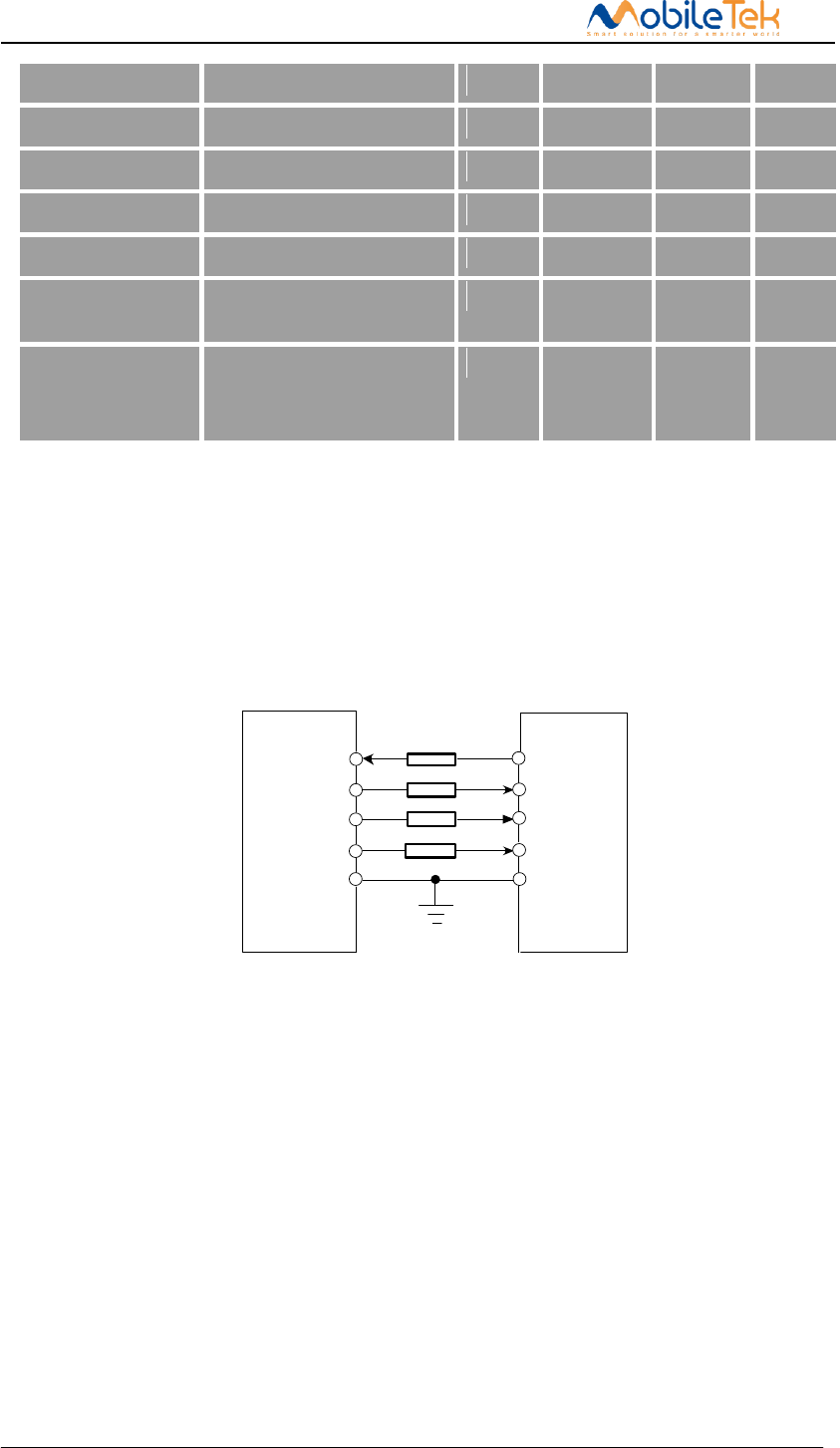
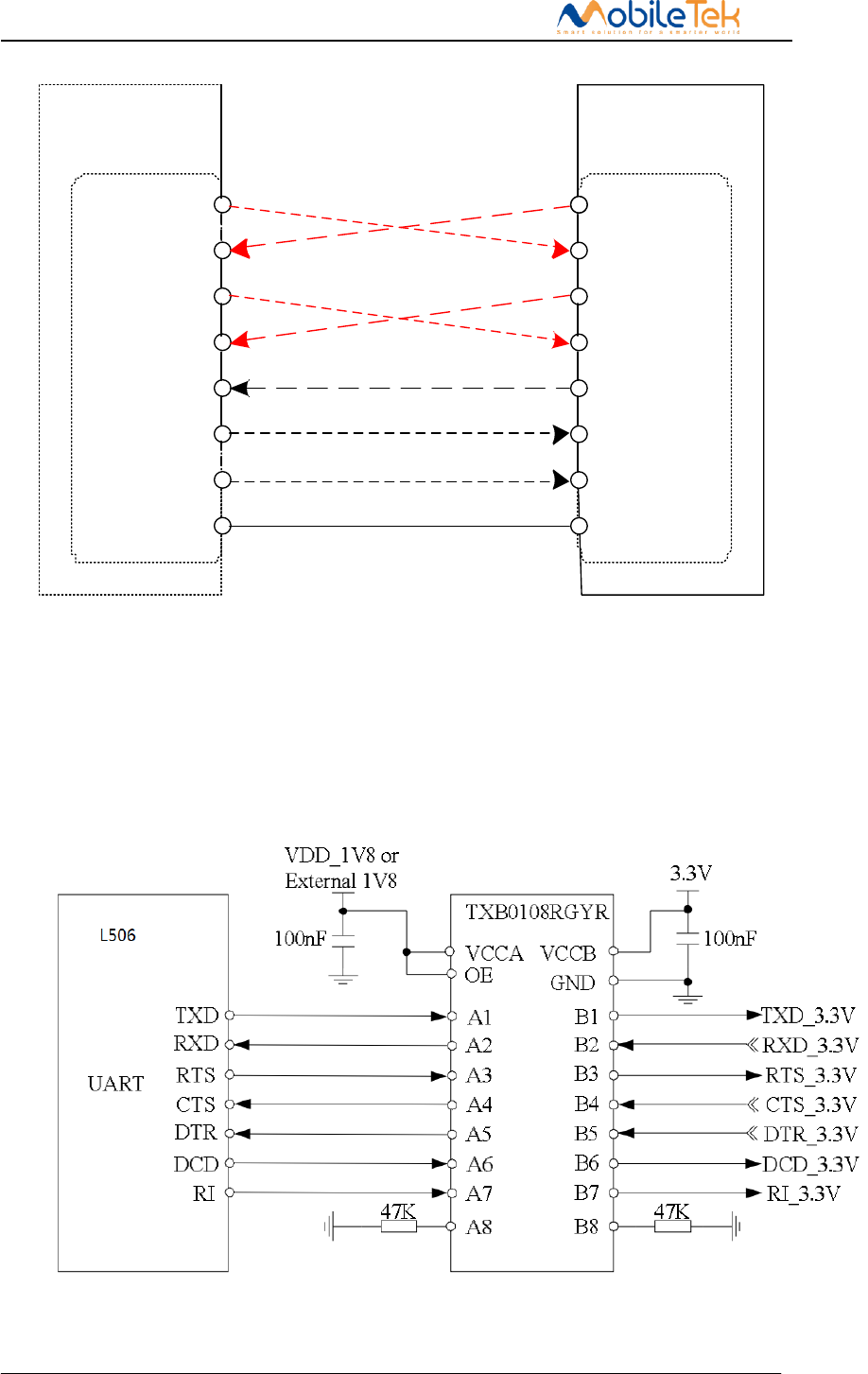
3.8 UART Interface
3.8.1 Pin description
L506 module provides a flexible 7-wire UART (universal asynchronous serial transmission)
interface. UART as a full asynchronous communication interface, Support the standard modem
handshake signal control, Comply with the RS - 232 interface protocols. And also support four wire
serial bus interface or the 2-wire serial bus interface mode, and the module can be through the UART
L506A HOST(P
C)
USB_DP
USB_DM
VBUS
GND
USB_ID
VBUS
USB_DP
USB_DM
GND
0R
47K
0R
L506 Hardware Design
Copyright © Shanghai Mobiletek Communication Ltd
interface for serial communication with the outside (DET) and the AT command input, etc. L506
module is a DCE (Data Communication Equipment) and client PC is a DTE (Data Terminal
Equipment).AT commands are entered and serial communication is performed through UART
interface. The pin signal is defined as shown in below table.
Table 3-14 UART pin definition
Pin No.
Pin
I/O type
Descriptions
71
UART_TX
DO
UART data transmission
68
UART_RX
DI
UART data receive
69
UART_RI
DO
Ring Indicator.
66
UART_RTS
DO
UART DET request to send
72
UART_DTR
DI
DTE get ready.
67
UART_CTS
DI
UART Clear to Send.
70
UART_DCD
DO
UART Carrier detects.
Note
:
UART_RI, UART_DTR can be used as two line UART interface for system debugging, See
table 3-3 Pin functional description.
3.8.2 UART interface application
UART_RI, UART_DTR default status is the system log port, so we recommend that users
keep reserved the interface and test points in design. The L506 UART is 1.8V interface. A level
shifter should be used if user’s application is equipped with a 3.3V UART interface. The level
shifter TXB0108RGYR provided by Texas Instruments is recommended. The reference design of
the TXB0108RGYR is in the following figures. About the application as below:
L506 Hardware Design
Copyright © Shanghai Mobiletek Communication Ltd
TXD1
RXD1
RTS1
CTS1
DTR1
DCD1
RING1
TXD
RXD
RTS
CTS
DTR
DCD
RING
Serial Port Serial Port
L506 (DCE) Client(DET)
GND GND
Figure 3-12 UART 4 Line connection mode
TXD1
RXD1
RTS1
CTS1
DTR1
DCD1
RING1
TXD
RXD
RTS
CTS
DTR
DCD
RING
Serial Port Serial Port
L506A(DCE) Client (DTE)
GND GND
Figure 3-13 UART 2 Line connection mode
L506 Hardware Design
Copyright © Shanghai Mobiletek Communication Ltd
TXD1
RXD1
RTS1
CTS1
DTR1
DCD1
RING1
TXD
RXD
RTS
CTS
DTR
DCD
RING
Serial Port Serial Port
L506 (DCE) Client (DTE)
GND GND
Figure 3-14 UART Full mode
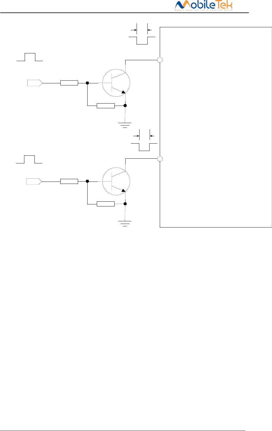
Figures 3-16 Voltage transfer Reference Circuit
L506 Hardware Design
Copyright © Shanghai Mobiletek Communication Ltd
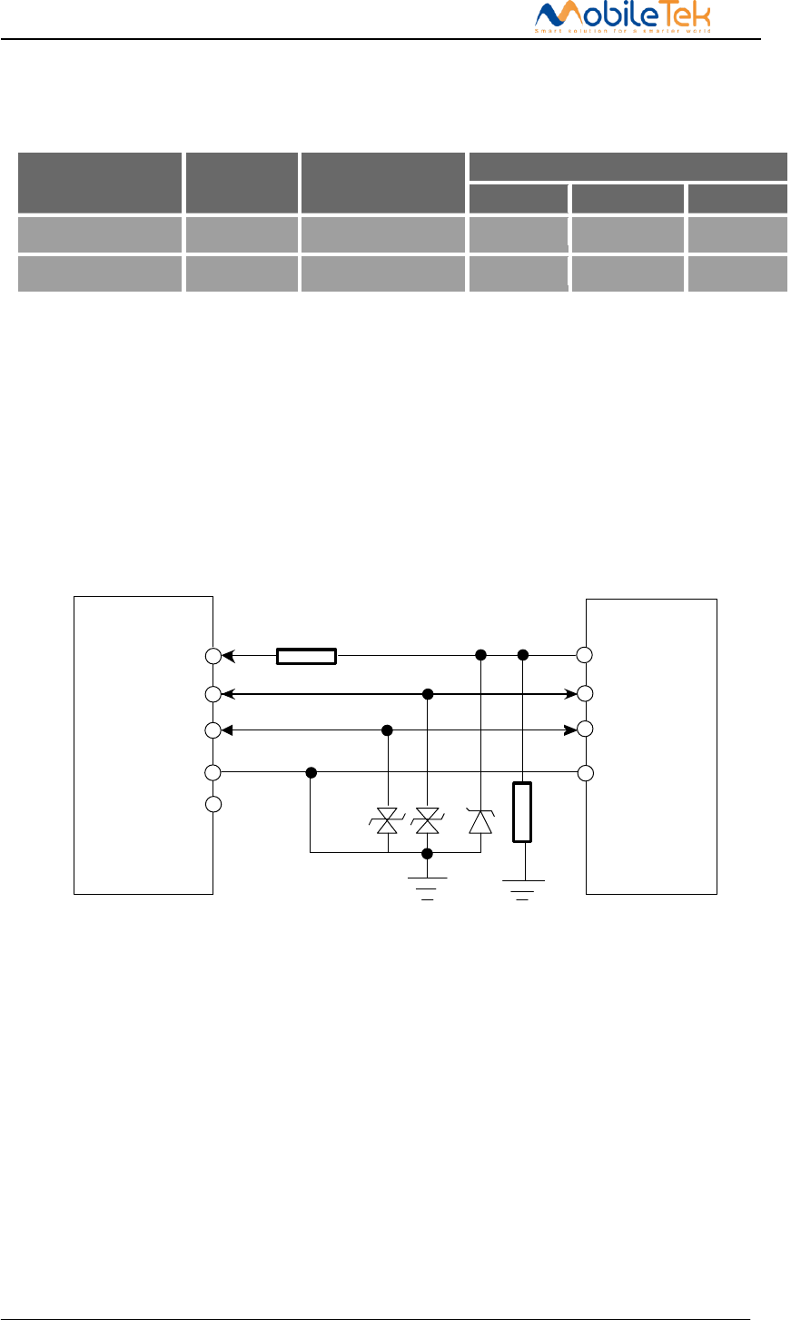
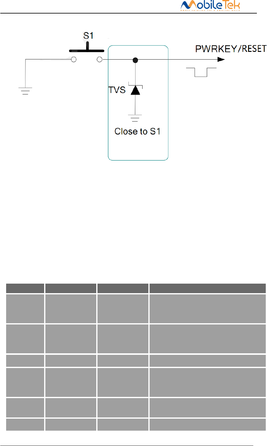
3.9 Power on/off and reset interface
3.9.1 Pin definition
L506 can be powered on by pulling PWRKEY pin down to ground. This pin is already internal
pulled up to 1.8V in module, so external pull-up resistor is not necessary. Placing a100nF capacitor
and an ESD protection diode close to the PWRKEY pin is strongly recommended. Please refer to the
following figure for recommended reference circuit L506 also have a RESET pin to reset module.
This function is used as an emergency reset only when AT command “AT+CPOF” and the PWRKEY
pin has no effect. User can pull RESET pin to ground, then module will reset. This pin is already
pulled up with a 40KΩ resistor to 1.8V in module, so external pull-up resistor is not necessary. Placing
a100nF capacitor and an ESD protection diode close to the RESET pin is strongly recommended.
Please refer to the following figure for recommended reference circuit, you can pull-down this pin to
ground and hold about 200 MS and then release will force the module enter reset state
AL
.
Table 3-15 power on/off and reset key define
Pin No.
Net name
I/O Typ.
descriptions
3
PWRKEY
DI
L506A power on/off pin (internal pull-up to
1.8V)
4
RESET
DI
L506A RESET pin (internal pull-up to 1.8V)
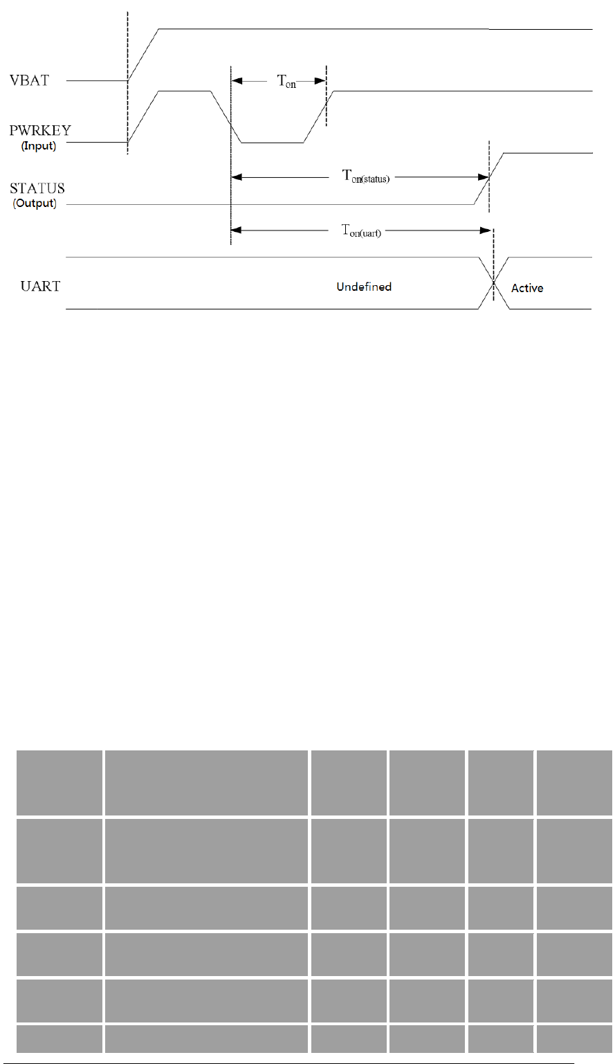
3.9.2 Power on sequence
Table 3-16 power on timing chart.
Ton
Power on low level pulse
100
500
--
ms
Ton(status)
Power on time (According to the
STATUS pin judgment)
15
--
25
s
Ton(uart)
Power on time (according the UART
pin judgement)
10
--
20
s
VIH
Input high level voltage of
PWRKEY pin
1.17
1.8
2.1
V
VIL
Input low level voltage of PWRKEY
pin
-0.3
0
0.3
V
L506A Hardware Design
Copyright © Shanghai Mobiletek Communication Ltd
Figures 3-17 Power on Timing sequence
Note: the STATUS pin can be used to identify whether has been power on, when the module has
access to electricity and initialization is completed, the STATUS output high level, or has
maintained low level.
3.9.3 Power off sequence
The following methods can be used to power down. These procedures will make module
disconnect from the network and allow the software to enter a safe state, and then save data before
completely powering the module off.
●Method 1: Power off L506A by pulling the PWRKEY pin down
●Method 2: Power off L506A by AT command “AT+CPOF”
●Method 3: over-voltage or under-voltage automatic power down.
●Method 4: over-temperature or under-temperature automatic power down.
Note: 1. About the AT command “AT+CPOF” detail please refer document [1].
2. Over-voltage or under-voltage may cause automatic power down.
3. Over-temperature or under-temperature may cause automatic power down.
Table 3-17 Power off timing chart.
Toff
The time of active low level
pulse on PWRKEY pin to power off
module
2.5
--
--
s
Toff(status
)
The time from power-off issue to
STATUS pin output low level
(indicating power off)
6
--
--
s
Toff(uart)
The time from power-off issue to
UART port off
6
--
--
s
Toff-on
The buffer time from power-off
issue to power-on issue
0
--
--
V
VIH
Input high level voltage of
PWRKEY pin
1.17
1.8
2.1
V
VIL
Input low level voltage of PWRKEY
-0.3
0
0.3
V
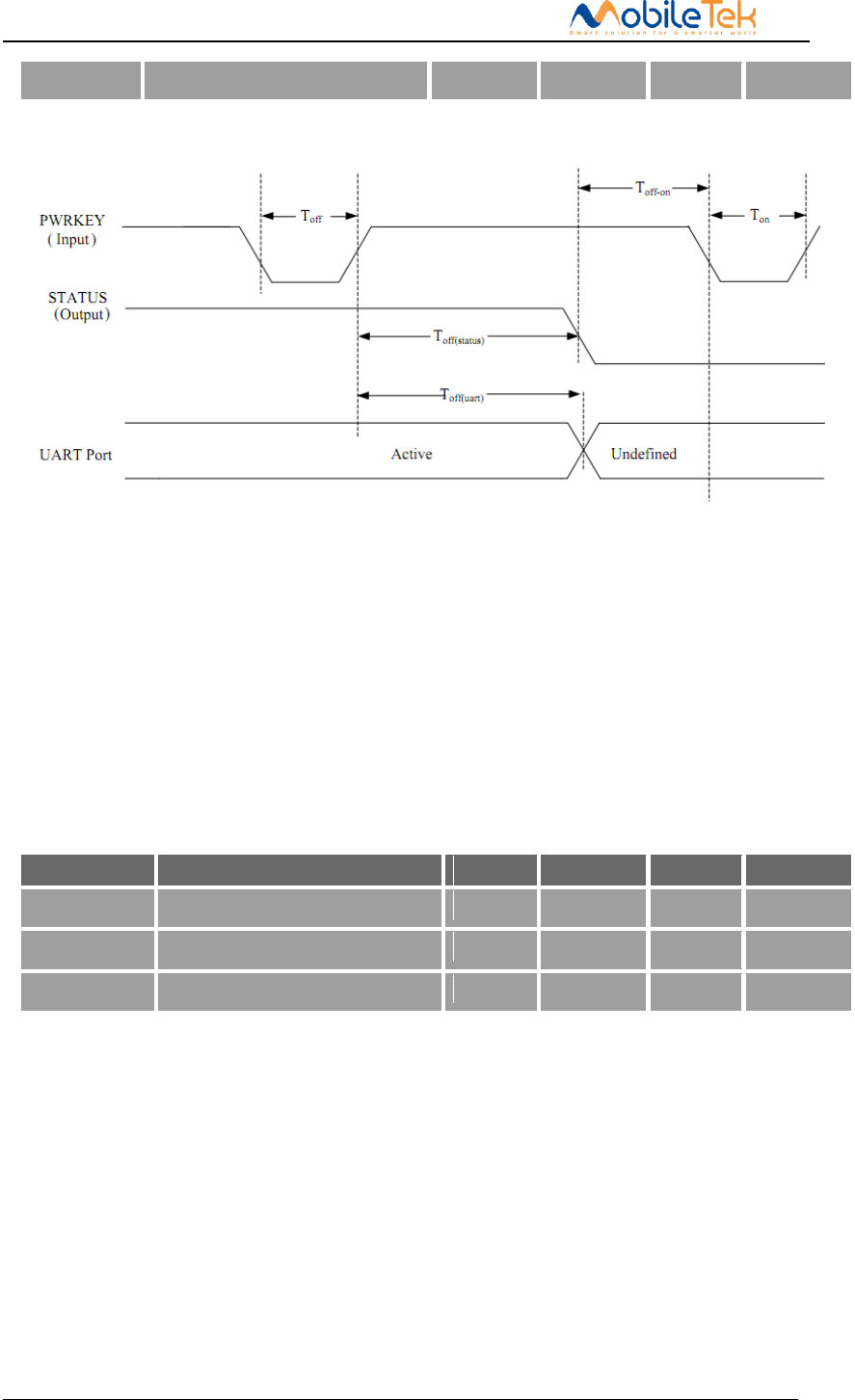
L506 Hardware Design
Copyright © Shanghai Mobiletek Communication Ltd
pin
User can power off the L506 by pulling PWRKEY down to ground for a specific time. The
power off scenario is illustrated in the following figure.
Figures 3-18 Power off Timing sequence
Note: the STATUS pin can be used to identify whether has been power on, when the module has
access to electricity and initialization is completed, the STATUS output high level, or has
maintained low level.
3.9.4 Reset sequence
L506 can lower module RESET pin to restart the module.
Table 3-18 Reset pin electrical properties
Symbol
Net name
Min.
Typ.
Max.
Unit
Treset
Reset pin low level hold time
50
100
500
ms
VIH
Reset pin input high level
1.17
1.8
2.1
V
VIL
Reset pin input low level
-0.3
0
0.3
V
Note: it is recommended that only in an emergency, such as module without response, use the
RESET pin. In addition, under the module power off status the RESET pin is invalid.
3.9.5 Power on/off and reset interface application
L506 Hardware Design
Copyright © Shanghai Mobiletek Communication Ltd
L506A
RESET
4.7K
47K
Pulse
PWRKEY
4.7K
47K
Pulse
500mS
500mS
Figure 3-19: Reference power on/off reset circuit
Another way to control the PWRKEY pin is directly using a push button switch. Need to set a button near
the TVS to ESD protection. The image below for reference circuit:
L506 Hardware Design
Copyright © Shanghai Mobiletek Communication Ltd
Figure 3-20: power on/off and reset recommended circuit (physical buttons)
3.10 Interactive interface
3.10.1 Pin definition
Table 3-19 list the interface is mainly with the application processor interactive interface,
including query, wake up four types, status indication, flight mode interface.
Table 3-19 Interactive interface
Pin No.
Signal
I/O type
Descriptions
50
GPIO_2/WAKEUP_IN
DI
Default: GPIO
Optional: Input pin as wake up interrupt
signal to module from host.
52
GPIO_1/WAKEUP_OU
T
Default: GPIO
Optional: Output pin as the module wake up
the AP
49
STATUS
DO
AP inquire the module status
54
FLGHTMODE
DI
Pull up to 1.8V made the system enter in
flight mode, at this mode will tune off all
the wireless function
45
GPIO_0
DO
General GPIO module output (used for
keyboard backlighting, etc.)
28
GPIO_3
I/O
GPIO
L506 Hardware Design
Copyright © Shanghai Mobiletek Communication Ltd
3.10.2 interactive interface application
L506 provides three shook hands with application processor communication signals.
Application processor can query whether the module boot normal work through STATUS. Through
the WAKEUP_OUT query module is in sleep mode, and sleep in the module, through
WAKEUP_IN wake module. Similarly, when application processor in the sleep state, the L506
modules can through WAKEUP_OUT wake application processor.
STATUS:Module sleep instructions, high level indicator to sleep, low level instructions for the
awakened state;
WAKEUP_IN: The host can lower the signal awakens the module,If, low level has maintained,
module can't sleep.
WAKEUP_OUT: when L506A need to communicate with the AP, module can be set this pin for low
level to awaken application processor.
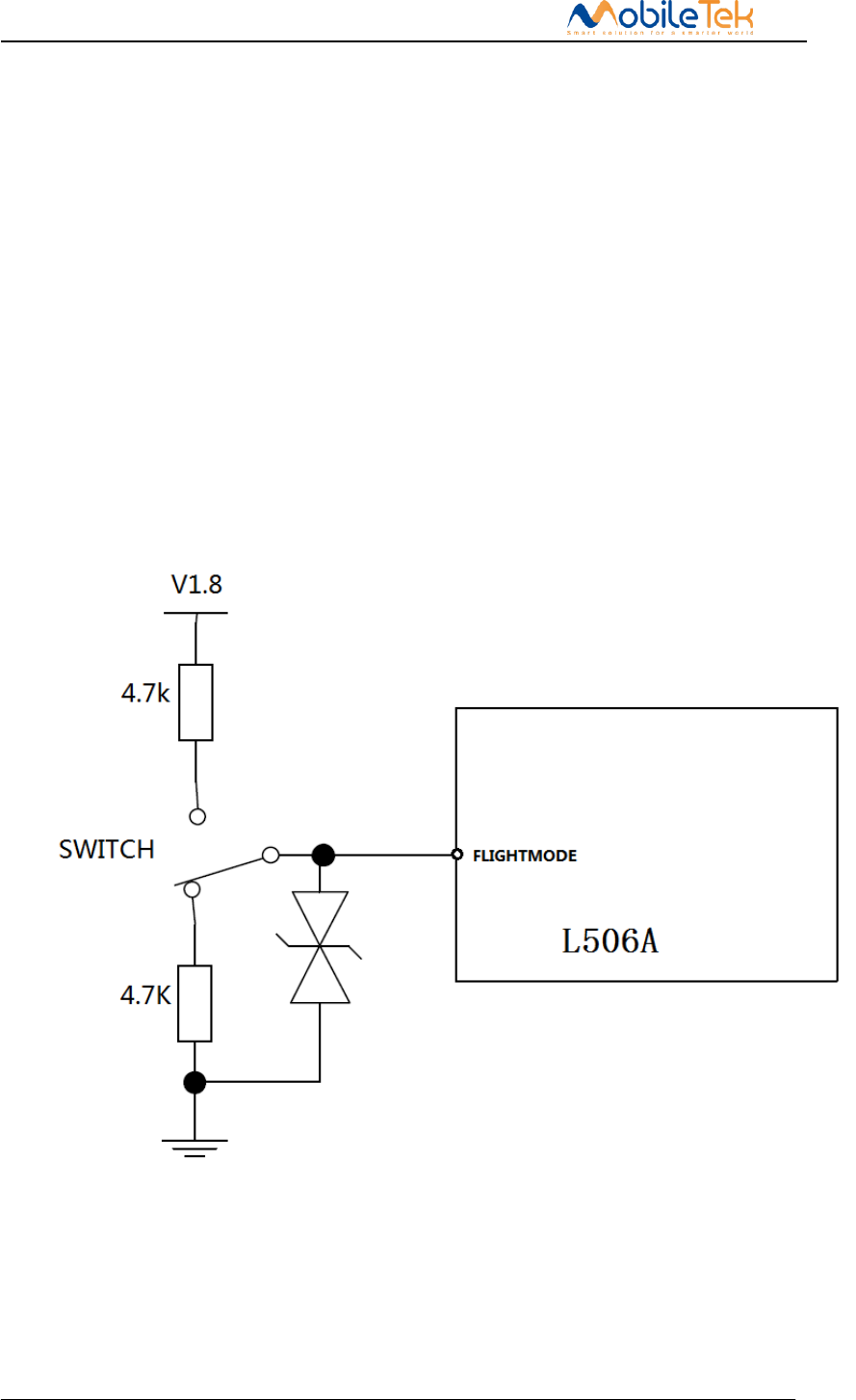
FLGHTMODE:Through the external output high level module into flight mode;
L506A
Figure 3-21: Flight mode recommended circuit (physical buttons)
L506 Hardware Design
Copyright © Shanghai Mobiletek Communication Ltd
3.11 Net Light interface
3.11.1 Pin define
Table 3-20 LED pin definitions
Pin No.
Net name
I/O type
description
51
NETLIGHT
DO
Module net state identify control LED port
3.11.2 Net light application
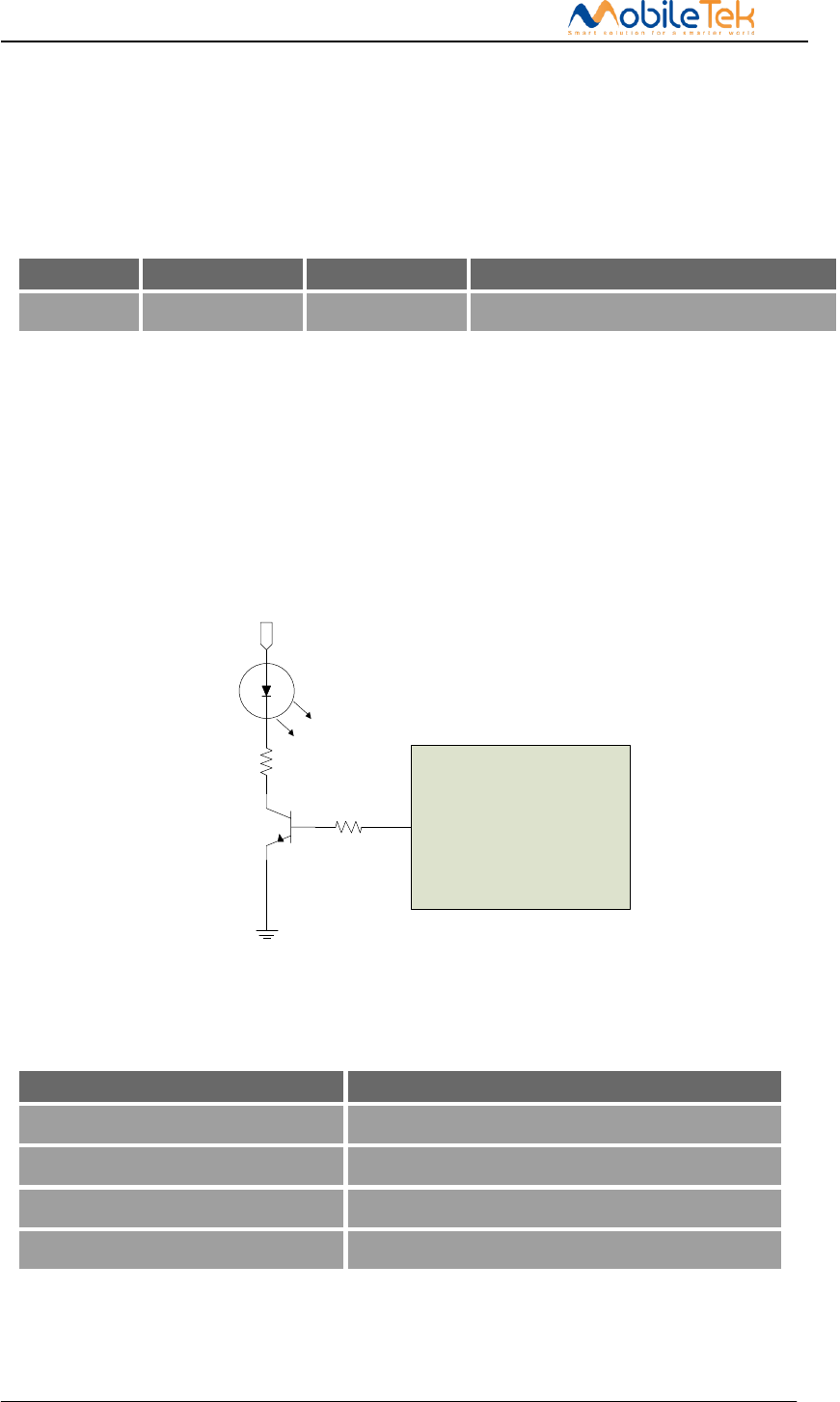
The L506 module has 1 pins for controlling the LED display, which can be used as an indicator
of network connection status. Different network states are represented by the mode of the flashing
light. This pin is an GPIO,with An external NPN Transistor,External connect VBAT can directly
drive LED. Drive current capacity varies according to external NPN model,recommend use
DTC143ZEBTL,Drive current biggest can reach 100 mA, below is the reference circuit.
L506A
LED
VLED
R2
R1
Figure 3-22 Status indicator reference circuit
Note: R1, R2 value according to the voltage VLED and LED working current.
Table 3-21 NETLIGHT status
Net Status
Module working status
Always on
Searching Network/Call Connect
200ms ON, 200ms OFF
Data Transmit
800ms ON, 800ms OFF
Registered network
OFF
Power off / Sleep
Note: NETLIGHT output low level as “ON”, and high level as “OFF”.
L506 Hardware Design
Copyright © Shanghai Mobiletek Communication Ltd
3.12 SD card interface
3.12.1 Pin descriptions
L506 provides a 4-bit SD/MMC interface with clock rate up to 52MHz. The operation voltage
of MMC/SD interface is 2.85V with SD/MMC memory cards up to 128G(FAT4), which is
compatible with SDIO Card Specification (version 3.0), Secure Digital (Physical Layer
Specification, version 3.0) and Multimedia Card Host Specification MMC (version 4.4)
Table 3-22 SD characteristics
Symbol
Parameter
Min.
Typ.
Max.
Unit
VDD_EXT**
LDO output
-
2.85
-
V
VIH
High-level input
voltage
0.625*VDD_
EXT
-
VDD_EXT+0.3
V
VIL
Low-level input
voltage
-0.3
0
0.25*VDD_EX
T
V
VOH
High-level output
voltage
2.75*VDD_E
XT
2.85
VDD_EXT
V
VOL
Low-level output
voltage
0
0
0.125*VDD_E
XT
V
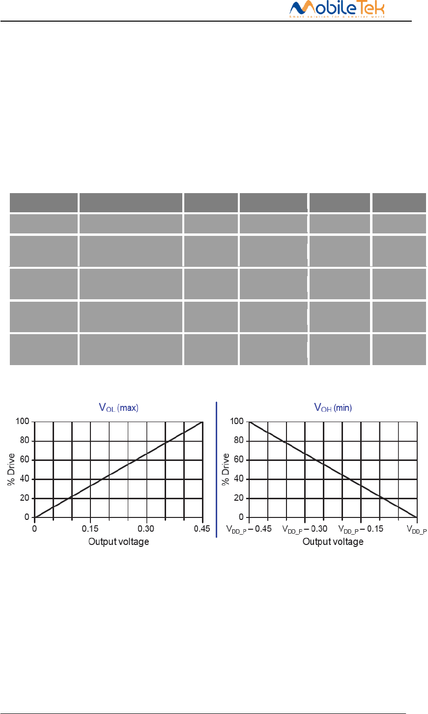
SD card I/O load capacity for linear output displacement, concrete can be calculated according to the
following chart;
Figure 3-23 VOL/VOH IV curve
3.12.2 SD card interface design guideline
L506 VDD_EXT for external SD card interface of power supply, in the card slot position should
add the ESD protection circuit; If you need to support SD hot plug design need to add SD_DET
signals. Due to the default hot plug pin of L506 check for low level to identify the card insert status,
so you need to choose the detect PIN connected to the ground when SD card is inserted into the SD
slot, below is the reference circuit.
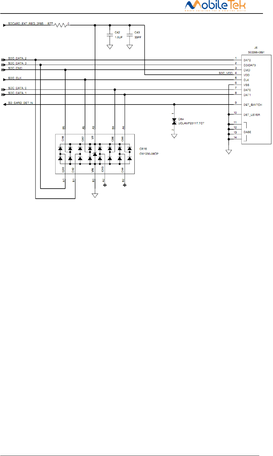
L506 Hardware Design
Copyright © Shanghai Mobiletek Communication Ltd
Figure 3-24 SD card recommended circuit
3.12.3 SD card signal PCB line rules
Due to the SD signal is the high-speed digital interface, so it’s layout rules should be in accordance
with the high speed digital rules.
1.Protect other sensitive signals/circuits from SDC corruption.
2. Protect SDC signals from noisy signals (clocks, SMPS, etc.).
3. 50 Ω nominal, ±10% trace impedance.
4. CLK to DATA/CMD length matching < 1 mm.
5. Total routing length < 50 mm recommended.
6. Spacing to all other signals = 2x line width.6 Bus capacitance < 15 pF.
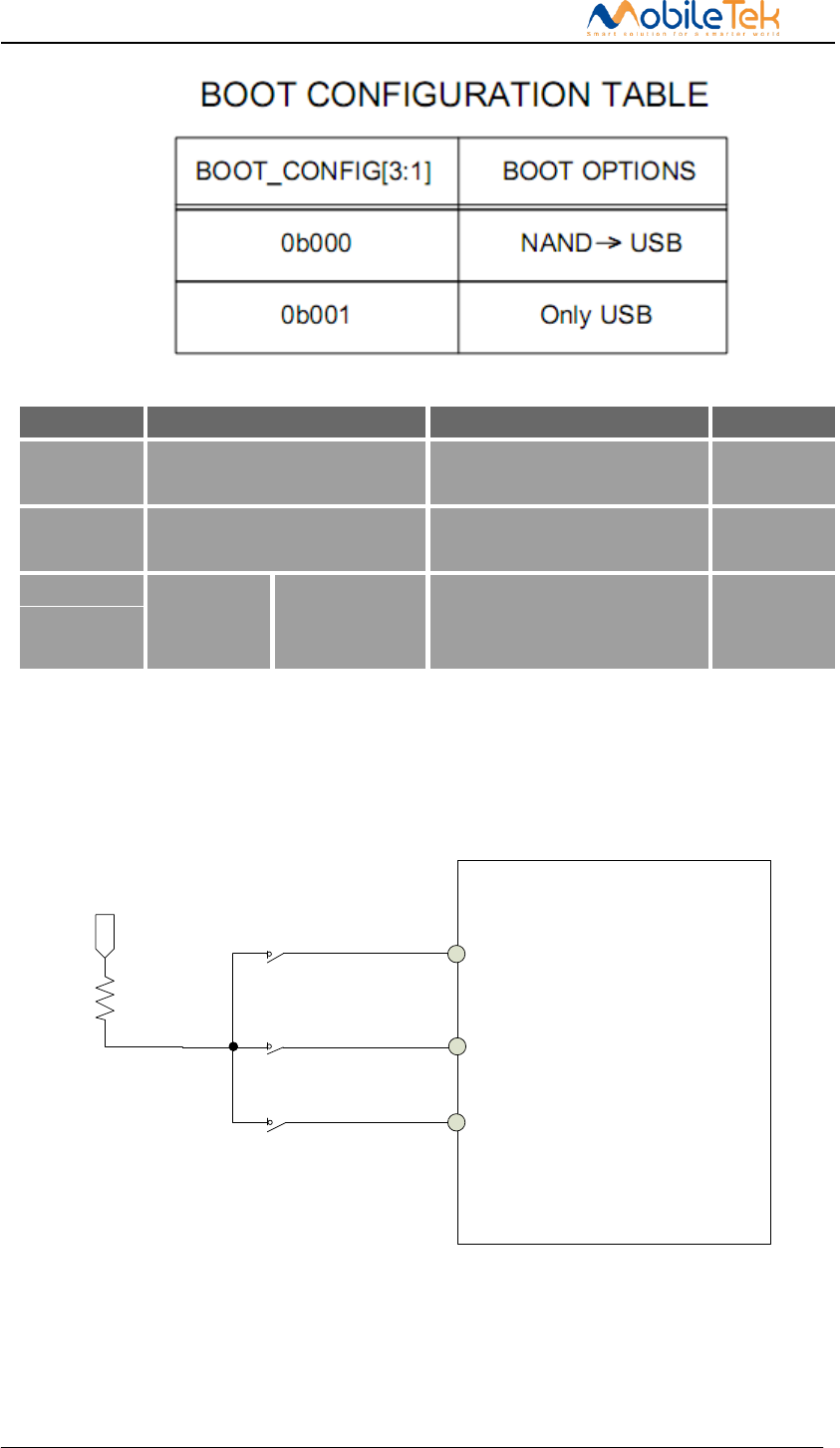
3.13 System boot configuration and download
3.13.1 Pin definition
L506 can configure BOOT_CONFIG (Boot Configuration) pin to Configuration module power-on
mode and the forced entry USB download mode.
L506 Hardware Design
Copyright © Shanghai Mobiletek Communication Ltd
Table 3-23 Boot configuration and force USB download
Pin No.
Net name
Function description
note
85
BOOT_CFG0
Pull up this pin change boot
configuration register value
87
BOOT_CFG1
Pull up this pin change boot
configuration register value
84
COEX2(Syste
m on)
FOCE_USB_BOOT
(before system
on)
Pull up this pin change boot
configuration register value
Multiplex
pin
3.13.2 Boot configuration and force USB interface application
Figure 3-25 boot configuration and force USB download recommended circuit
L506A
1.8V
BOOT_CFG0
10K
BOOT_CFG0
COEX2/FORCE_USB_BOOT
SW3
SW1
SW2
L506 Hardware Design
Copyright © Shanghai Mobiletek Communication Ltd
Input voltage range 0.3 -- VBAT V
Input resistance 1 -- -- MΩ
Note: 1. use "AT + CADC" and "AT + CADC2" can read ADC1 and ADC2 voltage on the pin.
More information please refer to the document [1].
2. The need for special software version to support access to the ADC.
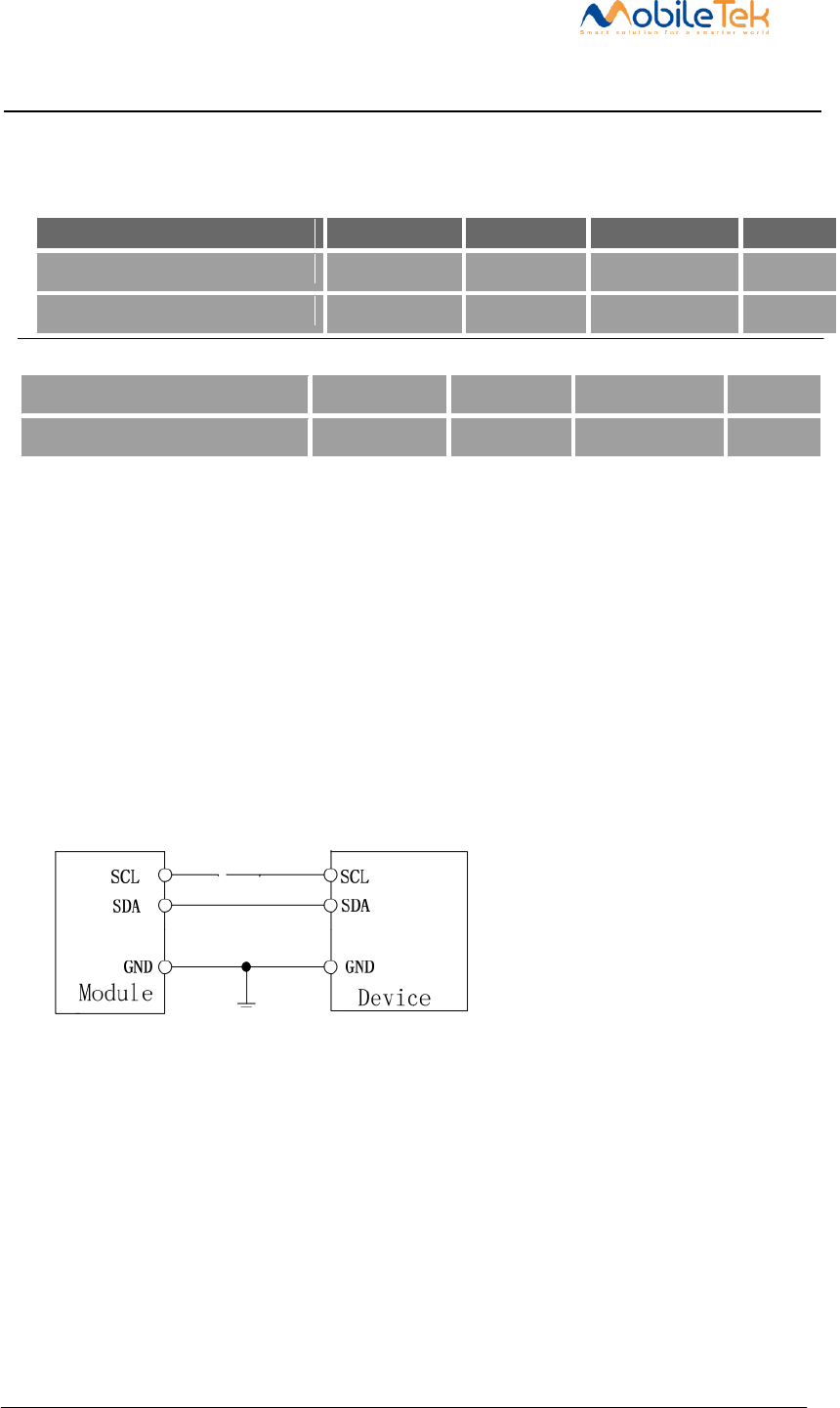
3.15 I2C interface
3.15.1 I2C pin definition
I2C is used to communicate with peripheral equipment and can be operated as either a transmitter or
receiver, depending on the device function. Both SDA and SCL are bidirectional lines connected with
I2C interface. Its operation voltage is 1.8V. High speed mode transmission rate can reach 400 KBPS,
Because L506 have internal pulled up to the I2C interface, so in your design needn’t pull up. Figure
3-15 is the reference design:
Figure 3-28 I2C reference design
Note: 1. L506 I2C only support host mode.
2. Only special software version support inquire the I2C.
3.16 Antenna interface
3.16.1 RF signal PCB layout guide
L506 provides RF antenna interface. Customer’s antenna should be located in the host board and
connected to module’s antenna pad through micro-strip line or other types of RF trace and the trace
impedance must be controlled in 50Ω. we recommends that the total insertion loss between the
antenna pad and antenna should meet the following requirements:
Copyright © Shanghai Mobiletek Communication Ltd 50
3.14 Analog and Digital conversion (ADC) interface
L506 integrated two analog-to-digital conversion interface, specific parameters are as follows:
Table 3-25 ADC1, ADC2 characters
characters Min. Typ. Max. Unit
ADC resolution -- 15 -- Bits
Transfer time -- 442 -- ms
L506 Hardware Design
Copyright © Shanghai Mobiletek Communication Ltd
●WCDMA 1900<0.9dB
●WCDMA 850<0.5 dB
●LTE (F<1GHz) <0.5dB
●LTE (1GHz<F<2GHz) <0.9dB
● LTE (2GHz<F) <1.2dB
To facilitate the antenna tuning and certification test, a RF connector and an antenna matching
circuit should be added. The following figure is the recommended circuit.
The antenna feed point is defined as shown in below table:
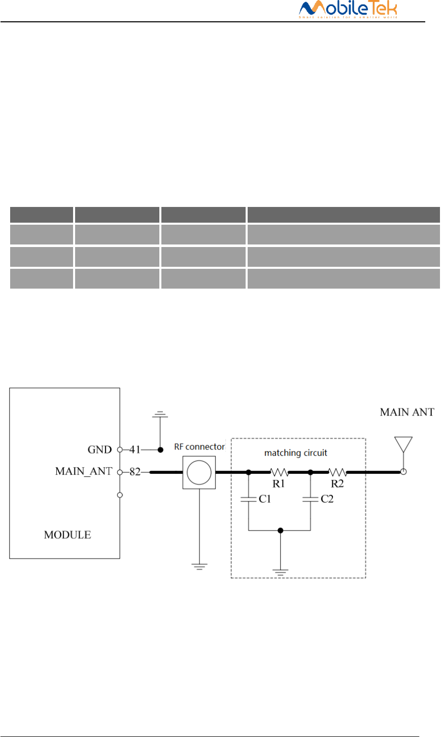
Table 3-26 antenna pin definition
Pin No.
Signal
I/O Typ.
Description
82
MAIN_ANT
AI/AO
Module main antenna
59
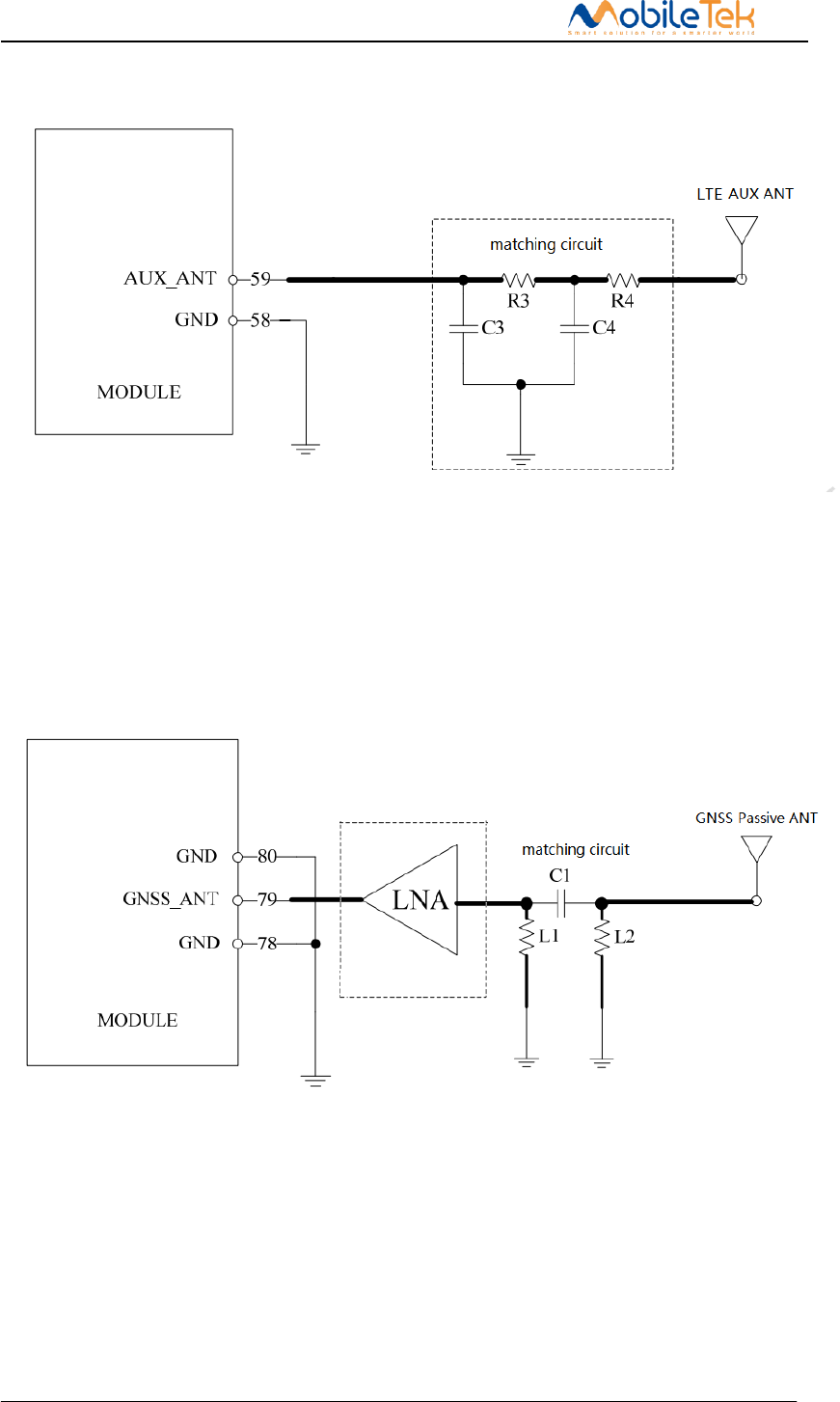
AUX_ANT
AI
LTE diversity antenna feed point
79
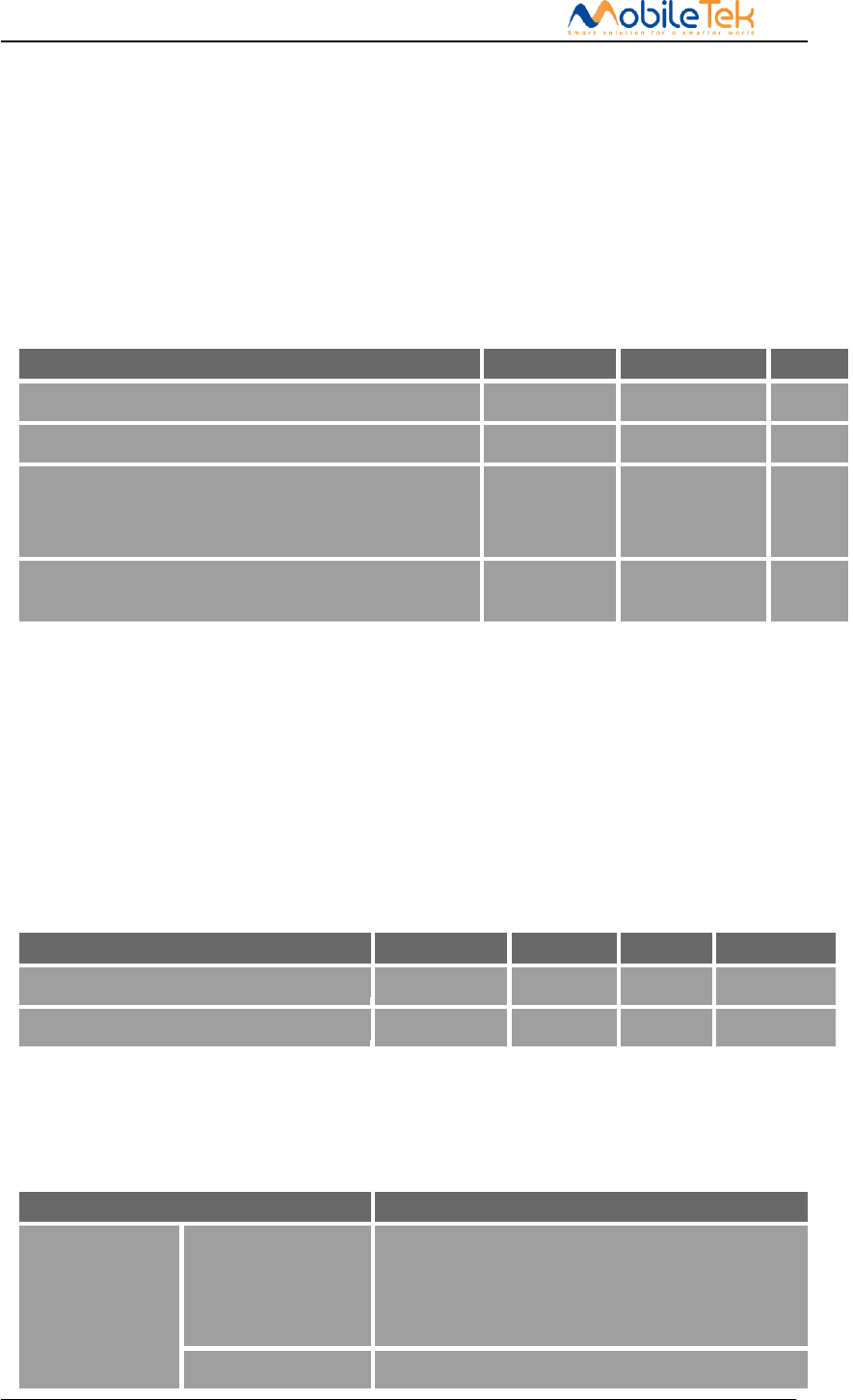
GNSS_ANT
AI
GNSS antenna feeder connector
3.16.2 applications
For convenience of antenna tuning and certification test, should increase RF connectors and the
antenna matching circuit, below is a recommended circuit:
Figure 3-29 Main antenna matching circuit diagram(MAIN_ANT)
In this figure, the components R1, C1, C2 and R2 is used for antenna matching, the value of
components can only be got after the antenna tuning, usually, they are provided by antenna vendor. By
default, the R1, R2 are 0 Ohm resistors, and the C1, C2 are reserved for tuning.
The RF test connector in the figure is used for the conducted RF performance test, and should be
placed as close as to the module’s antenna pin. The traces impedance between components must be
L506 Hardware Design
Copyright © Shanghai Mobiletek Communication Ltd 53
controlled in 50ohm.
Figure 3-30 LTE Diversity antenna matching circuit diagram(AUX_ANT)
Note:LTE diversity antenna recommend leaving. Because there are many high frequencies of
TDD LTE design, such as band38 band40 and Band41. Due to the high insertion loss RF line, if there
is no diversity antenna, receiving sensitivity of the spectrum in the certification will be a risk.
Figure 3-32 GNSS passive antenna matching circuit diagram(GNSS_ANT)
In above figures, the components C1 and L1, L2 are used for antenna matching, the values of the
components can only be obtained after the antenna tuning usually, and they are provided by antenna
vendor.C2 in Figure 3-19 is used for DC isolation. In active antenna circuit, users must use an external
LDO/DCDC to provide VDD voltage whose value should be taken according active antenna
characteristic, and VDD can be shut down to avoid consuming additional current when not being used.
GNSS can be used by NMEA port. User can select NMEA as output through UART or USB. NMEA
sentences are automatic and no command is provided. NMEA sentences include GSV, GGA, RMC,

L506 Hardware Design
Copyright © Shanghai Mobiletek Communication Ltd
GSA, and VTG. Before using GNSS, user should configure L506A in proper operating mode by AT
command.
Please refer to related document for details. L506 can also get position location information through
AT directly.
In the diagram above, component C1, L1 and L2 for antenna match, the element's value depends
on the antenna after debugging. In figure 3-18, C2 for dc isolation. In the active antenna circuit, the
user must use an external "/ DCDC VDD voltage, its value should be according to the properties of the
active antenna, VDD can close to avoid without additional current consumption when using GNSS. In
figure 3-19, the user can increase a external LNA gain to get better.
L506 merges GNSS (GPS/GLONASS) satellite and network information to provide a
high-availability solution that offers industry-leading accuracy and performance. This solution
performs well, even in very challenging environmental conditions where conventional GNSS receivers
fail, and provides a platform to enable wireless operators to address both location-based services and
emergency mandates.
●Tracking sensitivity: -159 dBm(GPS) -158 dBm(GLONASS)
●AcquisitionSensitivity: -148dBm
●Cold-start sensitivity: -142 dBm
●CN: C/N0 = S - (-170) S= Input Signal Intensity
●Accuracy (Open Sky) : 2.5m (CEP50)
●TTFF (Open Sky:) Hot start <1s Cold start 35s
●Receiver Type: 16-channel, C/A Code
●GPS L1 Frequency : 1575.42±1.023MHz
●GLONASS: 1597.5~1605.8 MHz
●BEIDOU: 1559.05~1563.14 MHz
●Update rate Default: 1 Hz
●GNSS data format: NMEA-0183
●GNSS Current consumption (WCDMA/Sleep mode) : 100mA (Total supply
current)
Antenna Layout guideline
In layout design, antenna RF transmission line must ensure the characteristic impedance = 50
ohm. The characteristic impedance depend on substrate board, line width and the distance from the
ground plane. As shown in figure 3-20 is the layout of antenna feed point of reference for clearance
area.

L506 Hardware Design
Copyright © Shanghai Mobiletek Communication Ltd
Figure 3-33 antenna feed point
L506 Hardware Design
Copyright © Shanghai Mobiletek Communication Ltd
4 Product characteristics
4.1 Absolute parameters
The following table shows the state of the absolute maximum work in abnormal situation. Exceed the limit
value will likely result in permanent damage to the module.
Table 4-1 L506A absolute parameters
Parameter
Min.
Max.
Unit
VBAT absolute voltage parameter
-0.5
6.0
V
USB_VBUS absolute voltage parameter
-0.5
5.25
V
I/O absolute voltage parameter:
PWRKEY, RESET, SPI, GPIO, I2C, PCM, UART,
SD1_DET,USIM_DET
-0.3
2.1
V
I/O absolute voltage parameter:
SD and USIM
-0.3
3.05
V
4.2 Operation condition
4.2.1 Operation voltage
This product is a DC input voltage range of 3.4 V to 4.2 V, the typical value of 3.8 V, as shown in below
table.
Table 4-2 Input DC voltage
Parameter
Min.
Typ.
Max.
Unit
VBAT Voltage
3.4
3.8
4.2
V
USB_VBUS Votage
2.0
5.0
5.25
V
About L506A dc electric property, please refer to part 3.3 digital I/O characteristics.
4.2.2 Work mode
Table 4-3 work mode
Mode
Description
Normal operation
mode
(WCDMA/LTE)Sleep
In this case, the current consumption of module
will be reduced to the minimal level.
In sleep mode, the module can still receive paging
message and SMS.
(WCDMA/LTE))
Software is active. Module is registered to the
L506 Hardware Design
Copyright © Shanghai Mobiletek Communication Ltd
Idle
WCDMA/ LTE network, and the module is ready to
communicate.
(WCDMA) taking
Connection between two subscribers is in progress.
In this case, the power consumption depends on
network settings such as DTX off/on, FR/EFR/HR,
hopping sequences, antenna.
(WCDMA/LTE)Standby
Module is ready for WCDMA/LTE
data transfer, but no data is currently sent or
received. In this case, power consumption depends
on network settings and /HSPA+ /LTE configuration.
(WCDMA/LTE) Data
transfer
There is WCDMA/LTE
data transfer in progress. In this case, power
consumption is related to network settings (e.g.
power control level); uplink/downlink data rates
Minimum mode
AT command “AT+CFUN” can be used to set the module
to a minimum functionality mode without removing
the power supply. In this mode, the RF
part of the module will not work or the USIM card
will not be accessible, or both RF part and USIM
card will be closed, and the serial port is still
accessible. The power consumption in this mode is
lower than normal mode.
Flight mode
Use the "AT + CFUN = 7" command or lower FLIGHTMODE
pins, the module can be configured to flight mode
under without removing the power supply condition.
In this case, the RF part does not work, but still
can use the serial port and USB, the power
consumption is lower than normal working mode.
Power off
Through the "AT + CPOF" command or lower PWRKEY pin
can power off L506A. At this mode, the module of
internal power supply will be closed, and the
system is stop running also. The UART and USB are
unavailable.
Sleep mode
In sleep mode, the module power consumption to a
minimum, but the module is still able to receive
paging information and SMS.
4.2.3 current consumption
The power consumption in suspended mode and without USB connection is listed in the table below.
Table 4-4 working current consumption (VBAT=3.8V)
GNSS (Without USB)
L506 Hardware Design
Copyright © Shanghai Mobiletek Communication Ltd
(AT+CFUN=0)
@ -140dBm,Positioning, Typical:72mA
Power off
Power off current
20uA
UMTS sleep/idle
WCDMA current
(GNSS off,without USB)
Sleep mode @DRX=9 typical:3.6mA
Idle mode @DRX=9 typical:19mA
LTE Sleep/Idle
LTE supply current
(GNSS off,without USB)
Sleep mode typical:3.8mA
Idle mode typical:TBD
UMTS Talking
WCDMA B2
@power 24dBm typical:665mA
WCDMA B5
@power 24dBm typical:586mA
HSDPA Data transmission
WCDMA B2
@power 24dBm typical:560mA
WCDMA B5
@power 24dBm typical:500mA
LTE Data transmission
LTE-FDD B2
@1.4Mbps typical:716mA
@3Mbps typical:656mA
@5Mbps typical:716mA
@10Mbps typical:722mA
@20Mbps typical:750mA
LTE-FDD B4
@1.4Mbps typical:616mA
@3Mbps typical:656mA
@5Mbps typical:656mA
@10Mbps typical:687mA
@20Mbps typical:721mA
LTE-FDD B5
@1.4Mbps typical:616mA
@3Mbps typical:656mA
@5Mbps typical:733mA
@10Mbps typical:766mA
LTE-FDD B13
5Mbps typical:591mA
@10Mbps typical:597mA
LTE-FDD B17
5Mbps typical:591mA
@10Mbps typical:597mA
L506 Hardware Design
Copyright © Shanghai Mobiletek Communication Ltd
4.3 Working and storage temperature
The operating temperature and storage temperature of L506A is listed in the following table.
Table 4-5 Operating temperature
Parameter
Min.
Typ.
Max.
Unit
Normal operation
temperature
-30
25
80
℃
Extended operation
temperature*
-40
25
85
℃
Storage temperature
-45
25
90
℃
*Note: Module is able to make and receive voice calls, data calls, SMS and make
WCDMA/HSPA+/LTE traffic in -40℃ ~ +85℃. Temperatures outside of the range -30℃ ~
+80℃ might slightly deviate from ETSI specifications.
4.4 ESD performance
L506A is electrostatic sensitive device, therefore, the user in the production, assembly and
operation of the module must pay attention to the electrostatic protection. L506A ESD performance
parameters in the following table:
Table 4-6 ESD performance parameters (temperature 25 ℃, humidity: 45%)
Net
contact
air
VBAT GND
±5KV
±10KV
Antenna port
±4KV
±8KV
UART
±2KV
±4KV
USB
±3KV
±6KV
Other PADS
±2KV
±4KV
5 Design guideline
This chapter provides a general design of the products instruction, the user can refer to design
guidance for design, make products to achieve better performance.

L506 Hardware Design
Copyright © Shanghai Mobiletek Communication Ltd
5.1 General design rules and requirements
Users in the design of this product is peripheral circuit, the first to ensure the external power
supply circuit can provide enough power supply capacity, And the requirements for high speed signal
lines USB control 90 ohm + / - 10% difference impedance. For general signal interface, require the
user to us in strict accordance with the requirements of design, in line with the interface signal level
matching, in case the level of damage to the module. This product its own radio frequency index is
good, customers need to design in accordance with the requirements the mainboard side antenna
circuit and corresponding impedance control, otherwise it will affect the whole RF index.
5.2 Reference circuit
Request system board VPH_PWR side power supply ability of power supply to achieve more
than 2 A, meet the demand of modules, peak current, and the system side the power of the average
current will reach more than 0.9 A. System board side power supply cord shall ensure enough line
width, and wants to form a good return with the ground plane, moreover should increase in the power
supply circuit design the method of micro level energy storage capacitor, guarantee the instantaneous
power supply capacity, and the power supply ripple control within the 100 mv, the specific function of
each functional module can be found in the corresponding description, overall reference circuit design
please refer《L506A reference design》.

L506 Hardware Design
Copyright © Shanghai Mobiletek Communication Ltd
5.3 RF part design guideline
5.3.1 Early antenna design considerations
Pre-project evaluation
The selection of the antenna position must first ensure that the antenna and the base station are
kept in the horizontal direction, this produces the highest efficiency; Secondly, try to avoid placing the
switch in the power supply or data line, chip and other devices or chips that produce electromagnetic
interference. At the same time, the position of the hand can be avoided, so as to prevent the human
body to produce attenuation; But also to reduce the radiation and the structure of the realization of the
need to take into account. So, At the beginning of the design need to structure, ID, circuit, antenna
engineers together to evaluate the layout.
Antenna matching circuit
If the module's radio frequency port and the antenna interface need to be transferred, the main
board circuit design, The design of microstrip line or strip line between the module RF test base and
the antenna interface between the microstrip line or the strip line by characteristic impedance 50 ohm,
at the same time, reserved double L type matching circuit; If the antenna's RF connector can be
directly stuck in the module's RF test base, can save the module of the RF port and the antenna
interface between the transfer.
5.4 EMC and ESD design advice
Users should take full account of the EMC problem caused by signal integrity and power integrity
in the design of the whole machine, In the module of the peripheral circuit layout, for power and signal
lines, etc., to maintain the spacing of 2 times line width. Can effectively reduce the coupling between
the signal, so that the signal has a clean, the return path. When the peripheral power supply circuit is
designed, the decoupling capacitor should be placed close to the module power supply pin, High
frequency high speed circuit and sensitive circuit should be far from the edge of PCB, and the layout
of the layout as far as possible to reduce the interference between each other, and the sensitive signal is
protected. The circuit or device that may interfere with the operation of the system board is designed.
This product is embedded in the system board side, design, need to pay attention to the ESD
protection, the key input and output signal interface, such as (U) SIM card interface need to be placed
close to the protection of ESD devices. In addition to the
motherboard side, the user is required to design the structure and PCB layout, ensure that the
metal shield is fully grounded, and set up an unobstructed discharge passage for the electrostatic
discharge.
L506 Hardware Design
Copyright © Shanghai Mobiletek Communication Ltd
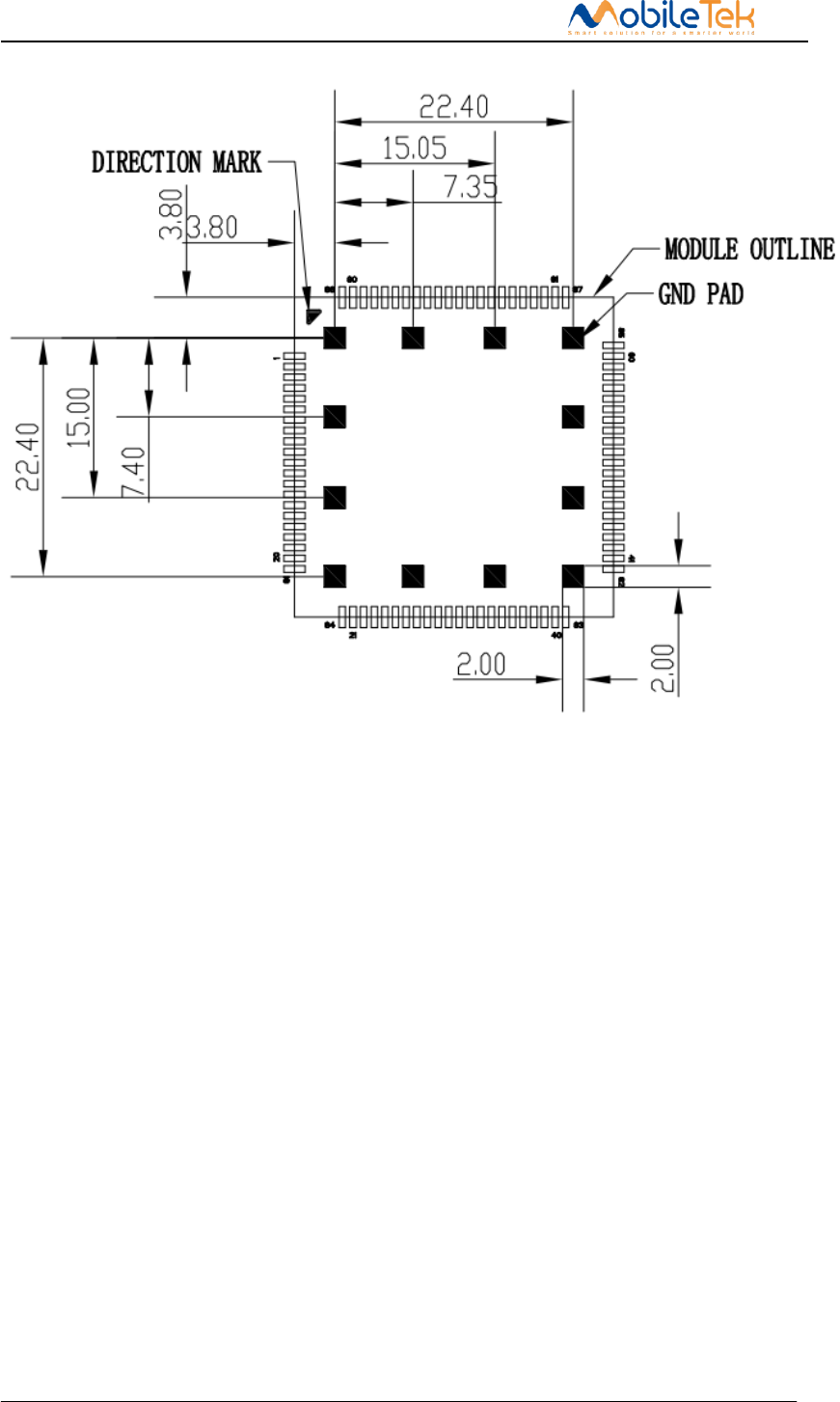
5.5 PCB Recommended land pattern
We recommend that users in the design of main board PCB DEF,In the middle of the 12
geothermal solder design according to size in below figure. Recommended at 87 of peripheral signal
pads to the module with a length of 1.0 mm. Recommended PCB pads as shown in below.
Figure 5-1 RECOMMENDED LAND PATTERN (Unit: mm)(detail A)
L506 Hardware Design
Copyright © Shanghai Mobiletek Communication Ltd
Figure 5-2 RECOMMENDED LAND PATTERN (Unit: mm)(detail B)
5.6 Products recommended upgrade
L506 default through the USB firmware updates, so products to facilitate the software update,
when the design proposal to set aside the USB test points or interface to facilitate subsequent product
of the firmware upgrade.
L506 Hardware Design
Copyright © Shanghai Mobiletek Communication Ltd
6 Manufacturers
6.1 Steel mesh design
At the bottom of the module pad thermal, can be reduced by way of steel mesh
openings, reduce the risk of short circuit between the thermal and the module of the module Pin, have
certain effect;
Module pad thermal welded steel mesh openings are recommended for reference. Figure
6-1 and Figure 6-2 is recommended for steel mesh and size.
Figure 6-11 Steel mesh (unit mm)(detail A)
L506 Hardware Design
Copyright © Shanghai Mobiletek Communication Ltd
Figure 6-2 Steel mesh (unit mm) (detail B)
Note: The direction mark point only for identify the pin 1 position, should not embody in the steel
mesh file.
L506 Hardware Design
Copyright © Shanghai Mobiletek Communication Ltd
6.2 Temperature curve
The temperature curve of the welding quality and material status influence, please pay special
attention. Temperature rise speed should not be too fast, from room temperature to 150, the
temperature rise rate is less than 3s. At the same time in more than 217 degrees, please try to keep time
no more than 70 seconds, at intermediate values of 55 seconds is appropriate. The thermal shock
strength is too general will lead to part of the device failure, resulting in a decline in yield and
maintenance difficulty. And please control the maximum temperature of no more than 245 degrees,
partial material, such as crystal at high temperature easy to occur the package rupture, cause unable to
play the problem, and then affect the function of the product, The temperature can be set using the
curve shown in table 6-1.
Table 6-1 Temperature curve
Lead-free process temperature curve
Stage
Temperature
time
Preheat
Temperature rise from room
temperature to 150
rate of temperature rising
<3 / ℃ s
keep warm
150℃~200℃
40~110 s
Welding
< 217℃
40~70 s
< 230℃
15~45 s
Peak temperature
MAX:245℃
MIN:230℃
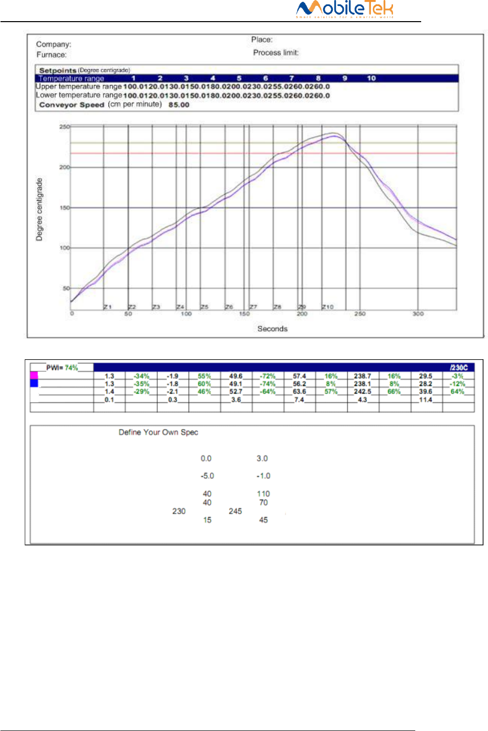
L506 Hardware Design
Copyright © Shanghai Mobiletek Communication Ltd
Module edge point
Module bottom
Chip
Temperature difference
Process limit
Butter of antimony:
Statistic name Lower limit Upper limit
Maximum temperature ascending slope (target: 2.0)
(Time distance = 20 seconds)
Maximum temperature descending slope
(Time distance = 20 seconds)
Preheat time 150200C
Time of the reflow temperature or above271C
Maximum temperature
Time of the temperature above 230C
Degree per second
Degree per second
Degree centigrade
Seconds
Seconds
Seconds
Unit
Upper limit
Preheat time 150200C Time of the reflow temperature
or above271C
Maximum temperature
ascending slope
Maximum temperature
descending slope Total time
Figure 6-3 The reference temperature curve
L506 Hardware Design
Copyright © Shanghai Mobiletek Communication Ltd
7 Package Storage information
7.1 Package information
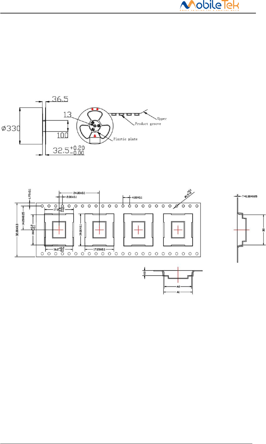
7.1.1 Tape and reel information
Figure 7-1 Tape and reel information
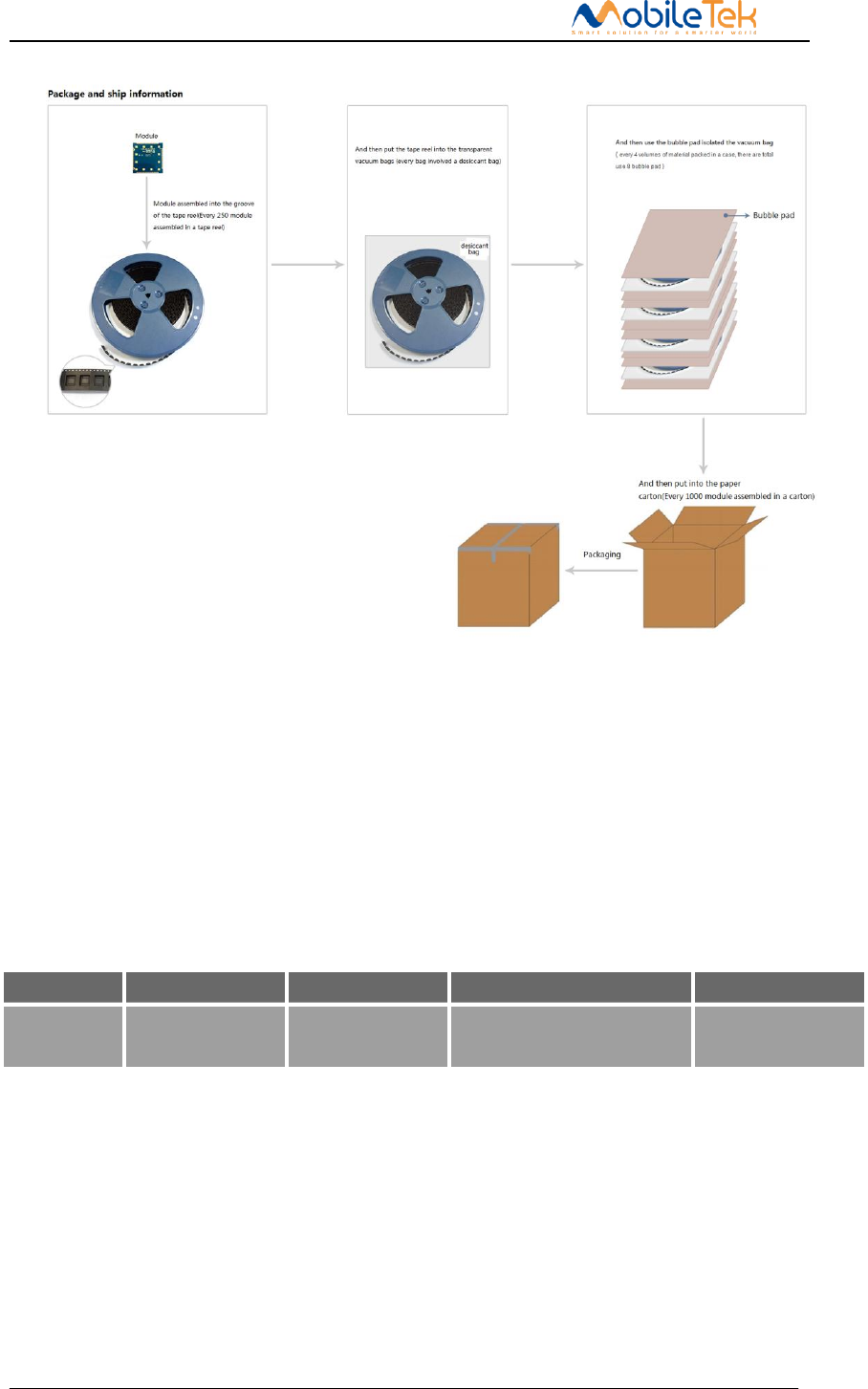
7.1.1 Package information
L506A packing diagram is as follows, every 4 volumes of material packed in a case between each volume of
material has a bubble mat do isolation protection. Specific as shown in the figure below:
L506 Hardware Design
Copyright © Shanghai Mobiletek Communication Ltd
Figure 7-2 Package and ship information
7.2 Bagged storage conditions
L506 shipments in the form of vacuum sealing anti-static bag. Module of storage need to follow the following
conditions: Environment below 40 Degrees Celsius temperature, air humidity is less than 90% of cases, the
module can be in vacuum sealed bags for 12 months. Conditions set the storage environment Suggestions
with reference to the following form.
Table 7-1 Storage conditions (less than 90% humidity of the air vacuum sealed packaging)
Parameter
Min.
Typ.
Max.
Unit
Storage
temperature
-45
25
90
℃
When on the vacuum bags, if meet the following conditions, the module can be directly for reflow soldering
(furnace temperature setting reference 6.2 furnace temperature curve) or other high temperature process:
Module temperature below 30 degrees c, the air humidity is less than 60%, factory within 72 hours to
complete the SMT.
The humidity is less than 10%.
If the module is in the following conditions, to be baked before SMT:
When the environment temperature is 23 degrees Celsius (allow upper and lower volatility of 5 degrees
Celsius), humidity index greater than 10%.
When open vacuum bags, module temperature below 30 degrees Celsius, air humidity is less than 60%,
but the factory have not finished the SMT within 72 hours.

L506 Hardware Design
Copyright © Shanghai Mobiletek Communication Ltd
When open the vacuum bags, module storage air humidity is more than 10%.
If modules need baking, please under 125 degrees Celsius (allowing fluctuations of 5 degrees Celsius) up
and down bake for 48 hours.
CONFIDENTIAL
Any Changes or modifications not expressly approved by the party responsible for compliance could void
the user’s authority to operate the equipment.
FCC Label Instructions:
If using a permanently affixed label, the modular transmitter must be labeled with its own FCC
identification number, and, if the FCC identification number is not visible when the module is
installed inside another device, then the outside of the device into which the module is installed must
also display a label referring to the enclosed module. This exterior label can use wording such as
the following: “Contains Transmitter Module FCC ID: 2AK9DL506” or “Contains FCC ID: 2AK9DL506".
Any similar wording that expresses the same meaning may be used.The Grantee may either
provide such a label, an example of which must be included in the application for equipment
authorization, or, must provide adequate instructions along with the module which explain this
requirement.
Single Modular Approval. Output power is conducted. This device is to be used in mobile or fixed
applications only. Antenna gain including cable loss must not exceed 10.42 dBi in Band 5, 9.5 dBi in
Band 2, 7 dBi in Band 4, 12.18 dBi in Band 13 and 11.77 dBi in Band 17 for the purpose of satisfying
the requirements of CFR 47 2.1043 & 2.1091. The antenna(s) used for this transmitter must be installed
to provide a separation distance of at least 20 cm from all persons and must not be co-located or operated
in conjunction with any antenna or transmitter, except in accordance with FCC multi-transmitter evaluation
procedure. Compliance of this device in all final product configurations is the responsibility of the Grantee.
Installation of this device into specific final products may require the submission of a Class II permissive
change application containing data pertinent to RF Exposure, spurious emissions, ERP/EIRP, and
host/module authentication, or new application if appropriate.
FCC Radiation Exposure Statement:
This equipment complies with FCC radiation exposure limits set forth for an uncontrolled
environment .This equipment should be installed and operated with minimum distance 20cm between the
radiator& your body.