Motorola Mobility T56DB2 Dual Band GSM Development Module User Manual g20 Cellular Engine Module Description
Motorola Mobility LLC Dual Band GSM Development Module g20 Cellular Engine Module Description
Contents
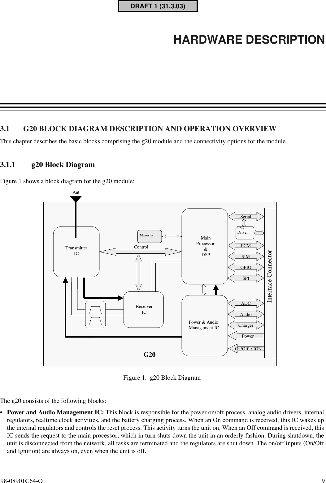
- 1. Exhibit 8 Users Manual
- 2. Exhibit 8 a1 Users Manual per CRN22341
- 3. Exhibit 8 b1 Users Manual per CRN22341
Exhibit 8 Users Manual