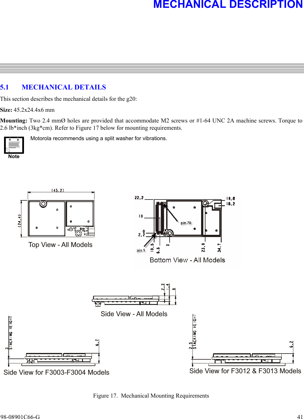
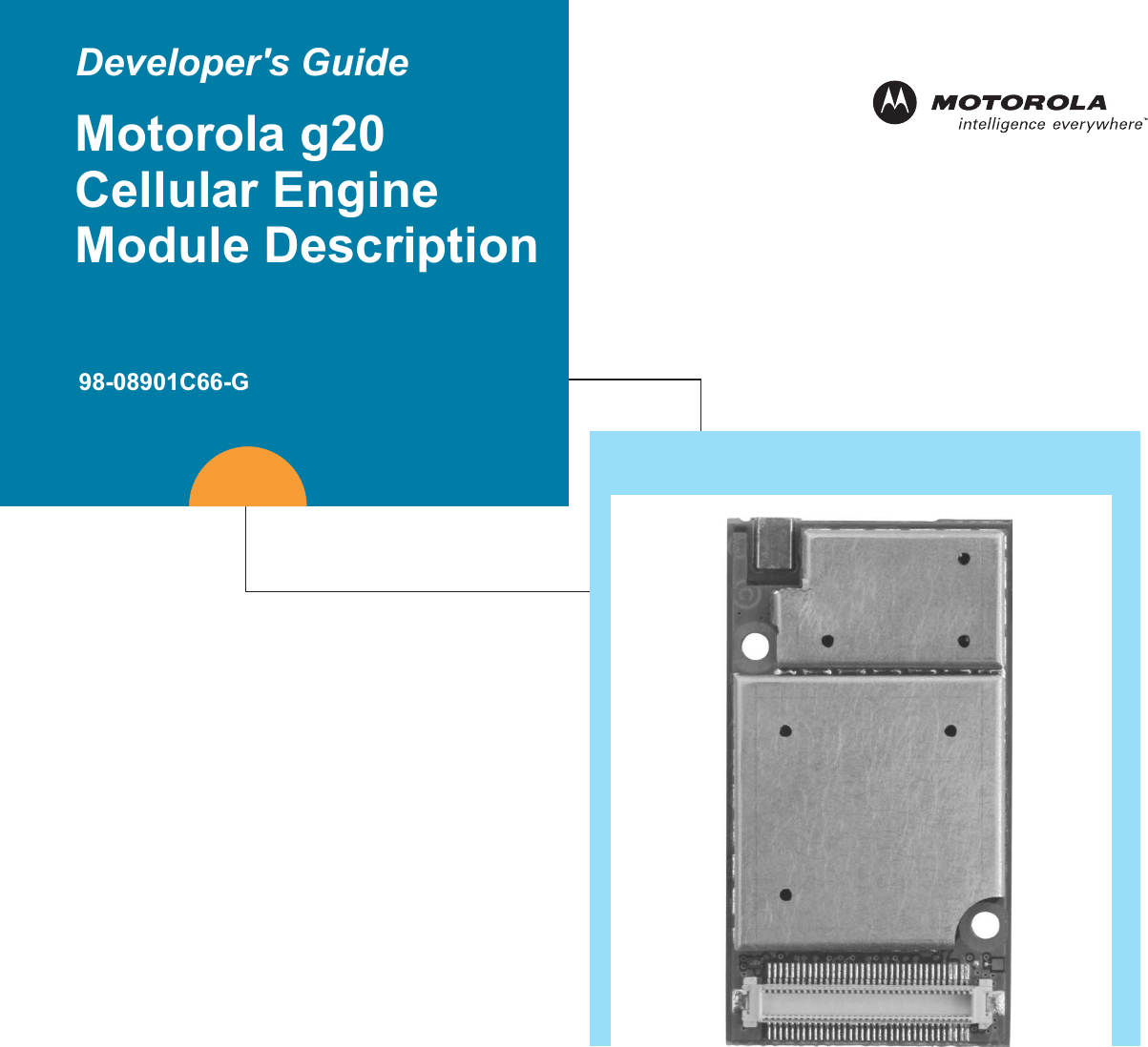
Motorola Mobility T56DB2 Dual Band GSM Development Module User Manual g20 Cell Engine Module Description

Motorola Mobility LLC Dual Band GSM Development Module g20 Cell Engine Module Description

Contents

Exhibit 8 a1 Users Manual per CRN22341

Developer's GuideMotorola g20Cellular EngineModule Description98-08901C66-G
SPECIFICATIONS SUBJECT TO CHANGE WITHOUT NOTICENoticeWhile reasonable efforts have been made to assure the accuracy of this document, Motorola, Inc. assumes no liability resulting from any  inaccuracies or omissions in this document, or from use of the information obtained herein. The information in this document has been carefully checked and is believed to be entirely reliable. However, no responsibility is assumed for inaccuracies or omissions. Motorola, Inc. reserves the right to make changes to any products described herein and reserves the right to revise this document and to make changes from time to time in content hereof with no obligation to notify any person of revisions or changes. Motorola, Inc. does not assume any liability arising out of the application or use of any product, software, or circuit described herein; neither does it convey license under its patent rights or the rights of others.It is possible that this publication may contain references to, or information about Motorola products (machines and programs), programming, or services that are not announced in your country. Such references or information must not be construed to mean that Motorola intends to announce such Motorola products, programming, or services in your country.CopyrightsThis instruction manual, and the Motorola products described in this instruction manual may be, include or describe copyrighted Motorola material, such as computer programs stored in semiconductor memories or other media. Laws in the United States and other countries preserve for Motorola and its licensors certain exclusive rights for copyrighted material, including the exclusive right to copy, reproduce in any form, distribute and make derivative works of the copyrighted material. Accordingly, any copyrighted material of Motorola and its licensors contained herein or in the Motorola products described in this instruction manual may not be copied, reproduced, distributed, merged or modified in any manner without the express written permission of Motorola. Furthermore, the purchase of Motorola products shall not be deemed to grant either directly or by implication, estoppel, or otherwise, any license under the copyrights, patents or patent applications of Motorola, as arises by operation of law in the sale of a product.Computer Software CopyrightsThe Motorola and 3rd Party supplied Software (SW) products described in this instruction manual may include copyrighted Motorola and other 3rd Party supplied computer programs stored in semiconductor memories or other media. Laws in the United States and other countries preserve for Motorola and other 3rd Party supplied SW certain exclusive rights for copyrighted computer programs, including the exclusive right to copy or reproduce in any form the copyrighted computer program. Accordingly, any copyrighted Motorola or other 3rd Party supplied SW computer programs contained in the Motorola products described in this instruction manual may not be copied (reverse engineered) or reproduced in any manner without the express written permission of Motorola or the 3rd Party SW supplier. Furthermore, the purchase of Motorola products shall not be deemed to grant either directly or by implication, estoppel, or otherwise, any license under the copyrights, patents or patent applications of Motorola or other 3rd Party supplied SW, except for the normal non-exclusive, royalty free license to use that arises by operation of law in the sale of a product.  VENDOR COPYRIGHTApache Software Foundation Copyright 2002-2003  All Rights ReservedArtesyn Copyright 2002-2003  All Rights ReservedCMU  * Copyright 2002-2003  All Rights ReservedFreeware Tools / Utilities  * Copyright 2002-2003  All Rights ReservedPerformance Technologies Copyright 2002-2003  All Rights ReservedTelelogic Copyright 2002-2003  All Rights ReservedQNX  * Copyright 2002-2003  All Rights Reserved*= Freeware
Usage and Disclosure RestrictionsLicense AgreementsThe software described in this document is the property of Motorola, Inc. and its licensors. It is furnished by express license agreement only and may be used only in accordance with the terms of such an agreement.Copyrighted MaterialsSoftware and documentation are copyrighted materials. Making unauthorized copies is prohibited by law. No part of the software or documentation may be reproduced, transmitted, transcribed, stored in a retrieval system, or translated into any language or computer language, in any form or by any means, without prior written permission of Motorola, Inc.High Risk MaterialsComponents, units, or third-party products used in the product described herein are NOT fault-tolerant and are NOT designed, manufactured, or intended for use as on-line control equipment in the following hazardous environments requiring fail-safe controls: the operation of Nuclear Facilities, Aircraft Navigation or Aircraft Communication Systems, Air Traffic Control, Life Support, or Weapons Systems (High Risk Activities"). Motorola and its supplier(s) specifically disclaim any expressed or implied warranty of fitness for such High Risk Activities.Trademarks MOTOROLA and the Stylized M Logo are registered in the US Patent & Trademark Office. All other product or service names are the property of their respective owners. ©Copyright 2005 Motorola, Inc.  Java™ Technology and/or J2ME™: Java and all other Java-based marks are trademarks or registered trademarks of Sun Microsystems, Inc. in the U.S. and other countries.UNIX®: UNIX is a registered trademark of The Open Group in the United States and other countries. REV052604
Developer’s Guide98-08901C66-G© Motorola Israel LTD., 2005A subsidiary of Motorola Inc.All rights reserved.g20 Cellular EngineModule Description
v  98-08901C66-GREVISION HISTORYRevision Date PurposeO 30 June 2003 Initial releaseA 05 November 2003 Minor corrections to the manualB 15 February 2004 Updated book versionUpdated section 2.3, Product SpecificationsUpdated section 2.5, Regulatory ApprovalsUpdated section 3.2.3.1, On/Off SignalUpdated Waking up the DTE diagram in section 3.2.4.2, DCE/DTE ConnectivityUpdated section 3.3.3.1, SIM ConnectionAdded section 3.3.5.3, Antenna DetectUpdated section 3.4.1.1, Analog InputRemoved 2 g20 modelsC 1 March 2004 Updated Table 13 - g20 Interface Connector Pin AssignmentsD July 2004 Updated section 3.2.1, Power Supply DesignUpdated section 3.2.1.1, Power Supply RF FilteringUpdated section 3.2.3.1, On/Off SignalUpdated section 3.2.3.2, Ignition SignalUpdated section 3.2.4.1, GeneralUpdated section 3.3.1, RS232Updated section 3.3.1.1, RS232 LevelsUpdated section 3.3.1.2, RS232 ConnectionUpdated section 3.3.2, USBUpdated section 3.3.2.1, USB ConnectionUpdated section 3.3.3.1, SIM ConnectionUpdated section 3.3.5.3, Antenna DetectUpdated section 3.4.1.1, Analog InputUpdated section 3.4.2, Digital Audio InterfaceUpdated section 3.5, Antenna
98-08901C66-G viUpdated table in section 4.2 and added notes, Pin AssignmentsUpdate section 6.1, Customer AssistanceE October 2004 Updated section 3.3.3.1, SIM Connection, and changed Figure 13Updated section 3.4.2, Digital AudioF March 2005 Updated section 3.2.3, Turning the Unit On/OffUpdated section 2.8.2, Antenna InstallationG April 2005 New sections: “LIMITATION OF LIABILITY” on page 2 and “WARRANTY NOTIFICATION” on page 3Revision Date Purpose
March 2005© Motorola Inc., 2004 98-08901C66-Gg20 Cellular EngineModule DescriptionCONTENTS REVISION HISTORY ................................................................................................................................................................vPREFACE1.1 SCOPE OF THIS MANUAL .................................................................................................................................................11.2 WHO SHOULD USE THIS MANUAL.................................................................................................................................11.3 APPLICABLE DOCUMENTS ..............................................................................................................................................11.3.1 Reference Documents .................................................................................................................................................11.3.2 Standards.....................................................................................................................................................................11.4 TRADEMARKS.....................................................................................................................................................................21.5 HOW THIS MANUAL IS ORGANIZED..............................................................................................................................21.6 LIMITATION OF LIABILITY..............................................................................................................................................21.7 WARRANTY NOTIFICATION ............................................................................................................................................31.7.1 HOW TO GET WARRANTY SERVICE?.................................................................................................................31.7.2 CLAIMING.................................................................................................................................................................31.7.3 CONDITIONS ............................................................................................................................................................41.7.4 WHAT IS NOT COVERED BY THE WARRANTY................................................................................................41.7.5 INSTALLED DATA...................................................................................................................................................51.7.6 OUT OF WARRANTY REPAIRS.............................................................................................................................5INTRODUCTION2.1 GENERAL DESCRIPTION...................................................................................................................................................72.2 TERMS AND ABBREVIATIONS ........................................................................................................................................72.3 PRODUCT SPECIFICATIONS.............................................................................................................................................92.4 MODELS DESCRIPTION...................................................................................................................................................112.5 REGULATORY APPROVALS...........................................................................................................................................112.6 REGULATORY REQUIREMENTS ...................................................................................................................................112.7 REGULATORY STATEMENT...........................................................................................................................................112.8 SAFETY PRECAUTIONS...................................................................................................................................................122.8.1 User Operation ..........................................................................................................................................................122.8.2 Antenna Installation ..................................................................................................................................................12
ix  98-08901C66-GHARDWARE DESCRIPTION3.1 G20 BLOCK DIAGRAM DESCRIPTION AND OPERATION OVERVIEW.................................................................. 133.1.1 g20 Block Diagram................................................................................................................................................... 133.1.2 Basic RS232 and Analog Audio Connectivity ......................................................................................................... 153.1.3 Basic RS232 and Digital Audio Connectivity*........................................................................................................ 153.1.4 Additional Recommended Connections ................................................................................................................... 163.2 POWER SUPPLY AND CURRENT CONSUMPTION..................................................................................................... 173.2.1 Power Supply Design ............................................................................................................................................... 173.2.2 g20 Current Consumption ........................................................................................................................................ 183.2.3 Turning the Unit On/Off........................................................................................................................................... 183.2.4 Sleep Mode Options ................................................................................................................................................. 193.3 COMMUNICATION INTERFACES.................................................................................................................................. 213.3.1 RS232 ....................................................................................................................................................................... 223.3.2 USB .......................................................................................................................................................................... 233.3.3 SIM ........................................................................................................................................................................... 243.3.4 SPI ............................................................................................................................................................................ 253.3.5 Unique g20 Interfaces............................................................................................................................................... 253.4 AUDIO INTERFACES........................................................................................................................................................ 263.4.1 Analog Audio Interfaces........................................................................................................................................... 263.4.2 Digital Audio Interface............................................................................................................................................. 303.5 ANTENNA........................................................................................................................................................................... 313.5.1 Antenna Performance Recommendations ................................................................................................................ 313.6 ESD PROTECTION ............................................................................................................................................................ 31CONNECTOR PIN ASSIGNMENTS4.1 CONNECTORS ................................................................................................................................................................... 334.2 PIN ASSIGNMENTS .......................................................................................................................................................... 34MECHANICAL DESCRIPTION5.1 MECHANICAL DETAILS.................................................................................................................................................. 41SERVICE SUPPORT6.1 CUSTOMER ASSISTANCE............................................................................................................................................... 436.1.1 Motorola Workflow.................................................................................................................................................. 446.1.2 Service Centers......................................................................................................................................................... 446.1.3 Ordering Accessories................................................................................................................................................ 456.2 TESTING A STANDALONE UNIT................................................................................................................................... 456.2.1 Test Setup ................................................................................................................................................................. 466.2.2 Test Procedure .......................................................................................................................................................... 46INDEX
98-08901C66-G xLIST OF FIGURESFigure 1. g20 Block Diagram..................................................................................................................................................... 13Figure 2. Basic RS232 and Analog Audio Connectivity ........................................................................................................... 15Figure 3. Basic RS232 and Digital Audio Connectivity ............................................................................................................ 16Figure 4. Additional g20 Connectivity....................................................................................................................................... 16Figure 5. VCC Signal During TX Periods ................................................................................................................................. 17Figure 6. On/Off Signal Timing Diagram.................................................................................................................................. 19Figure 7. CTS Sleep Mode Timing............................................................................................................................................ 20Figure 8. DCE/DTE Connectivity.............................................................................................................................................. 20Figure 9. Waking Up the g20 when the DTE wants to Send Data............................................................................................. 21Figure 10. Waking Up the DTE when the g20 wants to Send Data........................................................................................... 21Figure 11. g20 RS232 Interface ................................................................................................................................................. 22Figure 12. g20 USB Connection for g20 Models....................................................................................................................... 23Figure 13. g20 SIM Connection................................................................................................................................................. 24Figure 14. TX_EN Transmission ............................................................................................................................................... 25Figure 15. Antenna Detect ......................................................................................................................................................... 26Figure 16. Headset Speaker Output Measurement Configuration ............................................................................................. 27Figure 17. Mechanical Mounting Requirements........................................................................................................................ 41Figure 18. Test Setup ................................................................................................................................................................. 46
98-08901C66-G xiiLIST OF TABLESTable 1. Terms and Abbreviations ............................................................................................................................................... 7Table 2. Product Specifications.................................................................................................................................................... 9Table 3. g20 Models................................................................................................................................................................... 11Table 4. g20 Current Consumption............................................................................................................................................ 18Table 5. SPI Pinout..................................................................................................................................................................... 25Table 6. Headset Speaker Output at Maximum Volume Level ................................................................................................. 27Table 7. SPKR_N Output in Speaker Mode at Maximum Volume Level................................................................................. 28Table 8. SPKR_N Output when a 500mV RMS Signal is Transmitted..................................................................................... 28Table 9. SPKR_N Output when g20 is in Handset Mode.......................................................................................................... 29Table 10. Headset Speaker Output............................................................................................................................................. 29Table 11. Alert Transducer Levels for the ALERT_P Signal.................................................................................................... 30Table 12. Antenna Performance Recommendations .................................................................................................................. 31Table 13. g20 Interface Connector Pin Assignments................................................................................................................. 34
98-08901C66-G  11. PREFACE1.1 SCOPE OF THIS MANUALThis manual introduces the g20 embedded module and describes the technical details required by the user to successfullyintegrate the Motorola g20 cellular engine into an original equipment manufacturer (OEM) wireless host device. We at Motorola want to make this guide as helpful as possible. Keep us informed of your comments and suggestions forimprovements. You can reach us by email at: n2cshd@motorola.com.1.2 WHO SHOULD USE THIS MANUALThis manual is intended for all members of the integration team who are responsible for integrating the g20 module into the hostOEM device, including representatives from hardware, software and RF engineering disciplines. 1.3 APPLICABLE DOCUMENTS1.3.1 Reference Documents• g20 Developer's Kit - 9808901C67-D• g20 AT Commands - 9808901C68-F1.3.2 StandardsElectromagnetic Compatibility: Principles and Applications by David A Weston, published by Marcel Dekker, Inc., 270 Madi-son Avenue, New York, NY 10016 USA. GSM 07.07 - prETS 300 916, Digital cellular telecommunication system (Phase 2+); AT command set for GSM MobileEquipment (ME), Version 5.2.0 or higher, Reference RE/SMG-040707QR1.GSM 07.05, Digital cellular telecommunication system (Phase 2+); Use of Data Terminal Equipment - Data Circuit terminating;Equipment (DTE-DCE) interface for Short Message Service (SMS) and Cell Broadcast Service (CBS), Version 5.3.0, August,1997, ReferenceTS/SMG-040705QR2.GSM 03.40, Digital cellular telecommunication system (Phase 2+); Technical realization of the Short Message Service (SMS)Point-to-Point (PP), Version 5.3.0, July 1996, Reference TS/SMG-040340QR2.GSM 04.11 Digital cellular telecommunication system (Phase 2+); Point-to-Point (PP) Short Message Service (SMS) supporton mobile radio interface, Version 5.1.0, March 1996, Reference TS/SMG-030411QR.GSM 03.38, Digital cellular telecommunication system (Phase 2+); Alphabets and language-specific information, Version5.3.0, July 1996, Reference TS/SMG-040338QR2.
2  98-08901C66-GGSM 11.10-1, Digital cellular telecommunication system (Phase 2); Mobile Station (MS) Conformance specification; Part 1:Conformance specification. Draft pr ETS 300 607-1, March 1998, Reference RE/SMG-071110PR6-1.GSM Specifications are orderable from Global Engineering Documents, 15 Inverness Way East, Englewood, Colorado 80112-5704 USA 303-792-2181 800-624-3974.ETSI Standard PCS - 11.10-1.GSM 02.30 Supplementary services.GSM 03.90 USSD stage 2.GSM 11.14 SIM toolkit.ITU-T V.25terGSM Data Adapter for Motorola Handsets, AT command reference, Rev 2, June 9 1997. ETSI standard SMG31.GSM 05.02.ETSI 07.60.ETSI 0.7.07 Ver. 7.5.0.1.4 TRADEMARKSMOTOROLA and the Stylized M Logo are registered in the U.S. Patent and Trademark Office. All other product or servicenames are the property of their respective owners.©Motorola, Inc. 20051.5 HOW THIS MANUAL IS ORGANIZEDThis manual contains the following chapters: •Chapter 1 contains this Preface.•Chapter 2 introduces the g20 unit and provides important safety instructions.•Chapter 3 provides a detailed hardware description of the blocks and components comprising the g20.•Chapter 4 describes the pin assignments for g20 connectors.•Chapter 5 describes mechanical requirements for the g20 unit.•Chapter 6 provides contact information for Motorola Service Support and Customer Assistance.1.6 LIMITATION OF LIABILITY The Products are not designed, intended, or authorized for use as components in systems intended for surgical implant into thebody; in other applications intended to support or sustain life; for the planning, construction, maintenance, operation or use ofany nuclear facility; for the flight, navigation, communication of aircraft or ground support equipment; or in any other applica-tion in which the failure of the Product could create a situation where personal injury or death may occur. If CUSTOMER shoulduse any Product or provide any Product to a third party for any such use, CUSTOMER hereby agrees that MOTOROLA is notliable, in whole or in part, for any claims or damages arising from such use, and further agrees to indemnify and hold MOTOR-OLA harmless from any claim, loss, cost or damage arising from such use.  EXCEPT AS SPECIFICALLY STATED ABOVE, THE PRODUCTS ARE PROVIDED "AS IS" AND MOTOROLAMAKES NO OTHER WARRANTIES EXPRESS, IMPLIED, STATUTORY, OR OTHERWISE REGARDING THE PROD-UCTS. MOTOROLA SPECIFICALLY DISCLAIMS ANY IMPLIED WARRANTIES OF MERCHANTABILITY ANDFITNESS FOR A PARTICULAR PURPOSE, OR ARISING FROM A COURSE OF DEALING OR USAGE OF TRADE.
98-08901C66-G 3Under no circumstances shall MOTOROLA be liable to CUSTOMER or any other party for any costs, lost revenue or profitsor for any other special, incidental or consequential damages, even if MOTOROLA has been informed of such potential loss ordamage. And in no event shall MOTOROLA's liability to CUSTOMER for damages of any nature exceed the total purchaseprice CUSTOMER paid for the Product at issue in the dispute, except direct damages resulting from patent and/or copyrightinfringement, which shall be governed by the "INDEMNITY" Section of this Agreement.  The preceding states MOTOROLA's entire liability for MOTOROLA's breach or failure to perform under any provision of thisAgreement.1.7 WARRANTY NOTIFICATIONMotorola guarantees to you, the original purchaser, the Personal Communicator and accessories which you have purchased froman authorised Motorola dealer (the "Products"), to be in conformance with the applicable Motorola specifications current at thetime of manufacture for a term of [1] year from date of purchase of the Product(s) (Warranty Term).You must inform Motorola of the lack of conformity to the applicable specifications of any of the Products within a period oftwo (2) months from the date on which you detect a defect in material, workmanship or lack of conformity and in any eventwithin a term not to exceed the Warranty Term, and must immediately submit the Product for service to Motorola's AuthorisedRepair or Service Center. Motorola shall not be bound by Product related statements not directly made by Motorola nor anywarranty obligations applicable to the seller.A list of the Motorola Call Center numbers is enclosed with this Product.During the Warranty term, Motorola will, at its discretion and without extra charge, as your exclusive remedy, repair or replaceyour Product which does not comply with this warranty; or failing this, to reimburse the price of the Product but reduced to takeinto account the use you have had of the Product since it was delivered. This warranty will expire at the end of the WarrantyTerm.This is the complete and exclusive warranty for a Motorola Personal Communicator and accessories and in lieu of all otherwarranties, terms and conditions, whether express or implied.Where you purchase the product other than as a consumer, Motorola disclaims all other warranties, terms and conditions expressor implied, such as fitness for purpose and satisfactory quality.In no event shall Motorola be liable for damages nor loss of data in excess of the purchase price nor for any incidental specialor consequential damages* arising out of the use or inability to use the Product, to the full extent such may be disclaimed by law.This Warranty does not affect any statutory rights that you may have if you are a consumer, such as a warranty of satisfactoryquality and fit for the purpose for which products of the same type are normally used under normal use and service, nor anyrights against the seller of the Products arising from your purchase and sales contract.(*)including without limitation loss of use, loss of time, loss of data, inconvenience, commercial loss, lost profits or savings.1.7.1 HOW TO GET WARRANTY SERVICE?In most cases the authorised Motorola dealer which sold and/or installed your Motorola Personal Communicator and originalaccessories will honour a warranty claim and/or provide warranty service. Alternatively, for further information on how to getwarranty service please contact either the customer service department of your service provider or Motorola's call Center at thetelephone numbers below for your country.1.7.2 CLAIMINGIn order to claim the warranty service you must return the Personal Communicator and/or accessories in question to Motorola'sAuthorised Repair or Service Center in the original configuration and packaging as supplied by Motorola .Please avoid leavingany supplementary items like SIM cards. The Product should also be accompanied by a label with your name, address, andtelephone number; name of operator and a description of the problem. In the case of vehicular installation, the vehicle in which
4  98-08901C66-Gthe Personal Communicator is installed should be driven to the Authorised Repair or Service Center, as analysis of any problemmay require inspection of the entire vehicular installation.In order to be eligible to receive warranty service, you must present your receipt of purchase or a comparable substitute proofof purchase bearing the date of purchase. The phone should also clearly display the original compatible electronic serial number(IMEI) and mechanic serial number [MSN]. Such information is contained with the Product.You must ensure that all and any repairs or servicing is handled at all times by a Motorola Authorised Service Center in accor-dance with the Motorola Service requirementsIn some cases, you may be requested to provide additional information concerning the maintenance of the Products by MotorolaAuthorised Service Centers only, therefore it is important to keep a record of any previous repairs, and make them available ifquestions arise concerning maintenance1.7.3 CONDITIONSThis warranty will not apply if the type or serial numbers on the Product has been altered, deleted, duplicated, removed, or madeillegible. Motorola reserves the right to refuse free-of-charge warranty service if the requested documentation can not bepresented or if the information is incomplete, illegible or incompatible with the factory records.Repair, at Motorola's option, may include reflashing of software, the replacement of parts or boards with functionally equivalent,reconditioned or new parts or boards. Replaced parts, accessories, batteries, or boards are warranted for the balance of the orig-inal warranty time period. The Warranty Term will not be extended. All original accessories, batteries, parts, and PersonalCommunicator equipment that have been replaced shall become the property of Motorola. Motorola does not warrant the instal-lation, maintenance or service of the products, accessories, batteries or parts.Motorola will not be responsible in any way for problems or damage caused by any ancillary equipment not furnished by Motor-ola which is attached to or used in connection with the Products, or for operation of Motorola equipment with any ancillaryequipment and all such equipment is expressly excluded from this warranty.When the Product is used in conjunction with ancillary or peripheral equipment not supplied by Motorola, Motorola does notwarrant the operation of the Product/peripheral combination and Motorola will not honour any warranty claim where the Prod-uct is used in such a combination and it is determined by Motorola that there is no fault with the Product. Motorola specificallydisclaims any responsibility for any damage, whether or not to Motorola equipment, caused in any way by the use of the PersonalCommunicator, accessories, software applications and peripherals (specific examples include, but are not limited to: batteries,chargers, adapters, and power supplies) when such accessories ,software applications and peripherals are not manufactured andsupplied by Motorola.1.7.4 WHAT IS NOT COVERED BY THE WARRANTYThis warranty is not valid if the defects are due to damage, misuse, tampering, neglect or lack of care and in case of alterationsor repair carried out by unauthorised persons.The following are examples of defects or damage not covered by this product warranty1. Defects or damage resulting from use of the Product in other than its normal and customary manner.2. Defects or damage from misuse, access to incompatible sources, accident or neglect.3. Defects or damage from improper testing, operation, maintenance, installation, adjustment, unauthorised software appli-cations or any alteration or modification of any kind.4. Breakage or damage to antennas unless caused directly by defects in material or workmanship.5. Products disassembled or repaired other than by Motorola in such a manner as to adversely affect performance or preventadequate inspection and testing to verify any warranty claim.6. Defects or damage due to range, coverage, availability, grade of service, or operation of the cellular system by the cellularoperator.
98-08901C66-G 57. Defects or damage due to moist, liquid or spills of food.8. Control unit coil cords in the Product that are stretched or have the modular tab broken.9. All plastic surfaces and all other externally exposed parts that are scratched or damaged due to customer normal use.10. Leather cases (which are covered under separate manufacturer's warranties).11. Products rented on a temporary basis.12. Periodic maintenance and repair or replacement of parts due to normal wear and tear.The warranty for Motorola rechargeable batteries becomes void if (i) the batteries are charged other than by Motorola approvedbattery chargers specified for the charging of the battery, (ii) any of the seals on the battery are broken or show evidence oftampering, (iii) the battery is used in equipment or service other than the cellular telephone equipment for which it is specified.Depending on operating conditions and your usage habits, wear and tear might take place of components including mechanicalproblems related to Product housing, paint, assembly, sub-assemblies, displays and keyboards and any accessories which arenot part of the Product's in-box configuration. The rectification of faults generated through wear and tear and the use of consum-able items like batteries beyond their Optimum Performance Time as indicated in the product manual is considered to be yourresponsibility and therefore Motorola will not provide the free Warranty repair service for these items1.7.5 INSTALLED DATAPlease make and retain a note of all data you have inserted into your Product for example names, addresses, phone numbers,user and access codes, notes etc before submitting your Product for a Warranty service as such data may be deleted or erased aspart of the repair or service process.Please note if you have downloaded material onto your Product, for example ring tones, ring tunes, screensavers, wallpaper,games etc these may be deleted or erased as part of the repair process or testing process. Motorola shall not be responsible forsuch matters. The repair or testing process should not affect any such material that was installed by Motorola on your Productas a standard feature.1.7.6 OUT OF WARRANTY REPAIRSIf you request Motorola to repair your Product any time after the Warranty term or where this warranty does not apply due tothe nature of the defect or fault, then Motorola may in its discretion carry out such repairs subject to you paying Motorola itsfees for such a repair or it may refer you to an authorised third party to carry out such repairs.NoteThe talk-time, stand-by time and total life cycle of a Motorola rechargeable battery for your PersonalCommunicator will depend on usage conditions and network configurations. As a consumable product, thespecifications indicate that you should be able to obtain optimum performance for your Motorola PersonalCommunicator within the first six months from date of purchase and up-to (200) charges(Optimum Perfor-mance Time).
98-08901C66-G  72. INTRODUCTION2.1 GENERAL DESCRIPTIONThe g20 is Motorola’s newest family of embedded cellular products. Motorola continues its tradition of excellence byintroducing this new cellular engine family for GSM/GPRS communications, consisting of the d10, the d15 and the g18.The new module is similar to a condensed cellular phone core, and can be integrated in any system or product that needs totransfer voice or data information. Thus, it significantly enhances the system’s capabilities, transforming it from a standalone,isolated product to a powerful component connected to communication nets.The new g20 is extremely small in dimensions, yet packed with a host of highly-advanced features designed to facilitate fastand easy integration with OEM user products. It significantly shortens the development process for OEM developers, thanks toits wide range of built-in applications, and minimizes the product’s time to market.The g20 module is ideally suited for the automotive, telemetry, security, insurance and EPOS industries, for delivery andhandheld terminals, and for PDA markets.2.2 TERMS AND ABBREVIATIONSThis section provides definitions for terms and acronyms used in this document. Table 1. Terms and AbbreviationsAcronym/Term Definition/DescriptionAOC Advice of ChargeCSD Circuit-switched DataCTS Clear to SendDCD Data Carrier DetectDCE Data Communication Equipment (such as modems)DCS Digital Cellular System (GSM in the 1800MHz band)DOC Department of Communications (Canada)DSP Digital Signal ProcessorDSR Data Set ReadyDTE Data Terminal Equipment (such as terminals, PCs and so on)DTMF Dual-Tone Multi-FrequencyDTR Data Terminal ReadyEGSM Extended Global System for Mobile CommunicationsEIRP Effective Isotropic Radiated PowerEMC Electromagnetic CompatibilityEOTD Enhanced Observed Time DifferenceEPOS Electronic Point of SaleERP Effective Radiated Power
8  98-08901C66-GESD Electrostatic DischargeETSI European Telecommunication Standards InstituteFCC Federal Communications Commission (U.S.)FTA Full Type ApprovalGCF GSM Certification ForumGPIO General Purpose Input/OutputGPRS General Packet Radio ServiceGSM Global System for Mobile CommunicationsIC Integrated CircuitLNA Low-noise AmplifierMMCX Miniature Micro CoaxMO Mobile OriginatedMT Mobile TerminatedOEM Original Equipment ManufacturerPCB Printed Circuit BoardPCM Pulse Code ModulationPCS Personal Communication System (also known as GSM 1900)PDA Personal Data AssistantPDU Packet Data UnitPLL Phase-locked LoopPTCRB PCS-1900 Type Certification Review Board (GSM North America)R&TTE Radio and Telecommunications Terminal EquipmentRMS Root Mean SquareRI Ring IndicatorRTS Request To SendSAR Specific Absorption RateSIM Subscriber Identity ModuleSMS Short Message ServiceSPI Serial Peripheral InterfaceTDMA Time Division Multiple AccessUART Universal Asynchronous Receiver TransmitterUSB Universal Serial BusUSSD Unstructured Supplementary Services DataVCC Voltage Common CollectorVSWR Voltage Standing Wave RatioTable 1. Terms and Abbreviations (Continued)Acronym/Term Definition/Description
98-08901C66-G 92.3 PRODUCT SPECIFICATIONSTable 2. Product SpecificationsProduct FeaturesOperating systems: EGSM: 900/1800 MHzGSM: 850/1900 MHzPhysical CharacteristicsSize (F3003 - F3004):  45.2 x 24.4 x 6.7 mm height refer to the distance between the customer's board and the g20 top levelSize (F3012 - F3013): 45.2 x 24.4 x 6.2 mm height refer to the distance between the customer's board and the g20 top levelMounting: Two Ø2.4 mm holesWeight: 11.9 gramsEnvironmentalOperational temperature:  -20°C +70°CFunctional temperature: -30°C +85°CStorage temperature: -40°C +85°CPerformanceOperating voltage: Voltage: 3.0 - 4.2 VCurrent consumption: < 2.5 mA @ DRX9 (Idle mode)Tx power: • 0.8 W, 850 MHz• 2 W, 900 MHz• 1 W, 1800/1900 MHzInterfacesConnectors: • Single 70-pin, board-to-board•RF MMCXSIM Card: • Local SIM connectivity•32K SIM• 1.8/3.0 VSerial: • RS232:• BR from 300 bps to 115 Kbps• Auto BR from 300 bps to 115 Kbps•USB• 12 Mbps USB specifications, Rev. 1.1Data FeaturesGPRS: • Multi-slot class 8 (4 down; 1 up)• Max BR 85.6 Kbps• Class B GSM 07.10 multiplexing protocol• Coding scheme CS1-CS4CSD: Max BR 14.4 KbpsSMS: • MO/MT Text and PDU modes• Cell broadcastFAX Class 1
10  98-08901C66-GVoice FeaturesTelephonyDigital audioDifferential analog audio linesVocoders EFR/ER/FR/AMRDTMF supportAudio control: echo cancellation, noise suppression, side tone and gain controlGSM Supplementary ServiceUSSD Phase IICall forwardingCall hold, waiting and multipartyCall divertingMissed-call indicatorAOCCall barringCharacter SetUTF8UCS2Control/Status IndicatorsGPRS coverageWakeupTX enableResetAntenna DetectFeatures over RS232Embedded TCP/IP stackSTK Class IIEmergency and LocationFCC E911 Phase II Location Mandate using EOTDAT Command SetGSM 07.05GSM 07.07Motorola proprietary AT commandsAccessoriesFirmware data loaderData loggerDeveloper KitNoteSpecifications are subject to change without prior notice.Table 2. Product Specifications (Continued)
98-08901C66-G 112.4 MODELS DESCRIPTIONTable 3 lists the available g20 models.2.5 REGULATORY APPROVALSThe following regulatory approvals apply for the g20 module:•FCC• DOC• PTCRB•R&TTE•EMC•GCF2.6 REGULATORY REQUIREMENTSThe Federal Communications Commission (FEC) requires application for certification of digital devices in accordance withCFR Title 47, Part 2 and Part 15. This includes Electromagnetic Energy Exposure (EME) testing. As the g20 modem is not astandalone transceiver but is an integrated module, the g20 cannot be tested by itself for EME certification. It is, however, theintegrator’s responsibility to have the completed device tested for EME certification.2.7 REGULATORY STATEMENTThe following safety precautions must be observed during all phases of the operation, usage, service or repair of any cellularterminal or mobile incorporating the g20 module. Manufacturers of the cellular terminal are advised to convey the followingsafety information to users and operating personnel, and to incorporate these guidelines into all manuals supplied with the prod-uct. Failure to comply with these precautions violates safety standards of design, manufacture and intended use of the product.Motorola assumes no liability for customer failure to comply with these precautions.13. The g20 must be operated at the voltages described in the technical documentation.14. The g20 must not be mechanically nor electrically changed. Use of connectors should follow the guidance of the technicaldocumentation.15. The g20 is designed the meet the EMC requirements of ETS 300 342.16. When integrating the g20 into a system, Motorola recommends testing the system to ETS300342-1.17. The g20 meets the safety requirements of EN60950.18. Systems using the g20 are subject to mandatory EMC testing under directive 89/336/EEC (see item 3 above). Otherdirectives, such as the LVD directive 73/23/EE, may also apply to a system using the g20 module.Table 3. g20 ModelsModel Operating Bands Interface Connectors Serial InterfaceF3003 GSM 850/1900 • 70-pin 3 mm stacking height connector• MMCX RF connector USB/RS232F3004 EGSM 900/1800 • 70-pin 3 mm stacking height connector• MMCX RF connector USB/RS232
12  98-08901C66-G2.8 SAFETY PRECAUTIONS2.8.1 User OperationDo not operate your unit when a person is within 8 inches (20 centimeters) of the antenna. A person or object within 8 inches(20 centimeters) of the antenna could impair call quality and may cause the phone to operate at a higher power level than neces-sary.IMPORTANT: The unit must be installed in a manner that provides a minimum separation distance of 20 cm or more between the antenna and persons to satisfy FCC RF exposure requirements for mobile transmitting devices.IMPORTANT: To comply with the FCC RF exposure limits and satisfy the categorical exclusion requirements for mobiletransmitters, the following requirements must be met: 2.8.2 Antenna Installation• The antenna installation must provide a minimum separation distance of 20 cm from users and nearby persons and must notbe co-located or operating in conjunction with any other antenna or transmitter. • The combined cable loss and antenna gain must not exceed +9.9 dBi and total system output must not exceed 1.5 W ERP(Cellular) / 3.0 W EIRP (PCS) to qualify for categorical exclusion requirements of 2.1091. OEM installers must be providedwith antenna installation instruction and transmitter operating conditions for satisfying RF exposure compliance.
98-08901C66-G  133. HARDWARE DESCRIPTION3.1 G20 BLOCK DIAGRAM DESCRIPTION AND OPERATION OVERVIEWThis chapter describes the basic blocks comprising the g20 module and the connectivity options for the module.3.1.1 g20 Block DiagramFigure 1 shows a block diagram for the g20 module:Figure 1. g20 Block DiagramThe g20 consists of the following blocks:•Power and Audio Management IC: This block is responsible for the power on/off process, analog audio drivers, internalregulators, realtime clock activities, and the battery charging process. When an On command is received, this IC wakes upthe internal regulators and controls the reset process. This activity turns the unit on. When an Off command is received, thisIC sends the request to the main processor, which in turn shuts down the unit in an orderly fashion. During shutdown, theunit is disconnected from the network, all tasks are terminated and the regulators are shut down. The on/off inputs (On/Offand Ignition) are always on, even when the unit is off. MainProcessor&DSPMemoriesPower &AudioManagementICReceiverICControlUSBDriverPCMSIMGPIOInterface ConnectorSPIADCAudioChargerPowerOn/Off/IGNg20TransmitterICAntSerial
14  98-08901C66-G•Main Processor and DSP: This block is responsible for all the main tasks in the unit. It contains the following components: • Main processor• DSP for controlling speech options• UART• USB block• Digital audio driver• SIM card• Two SPI buses (one internal and one externally accessible)• Main clock (26 MHz)• Address/data buses• RF PLL• Controller to the RF ICs, which is the heart of the unit This module provides the following connectivity:• Address/data bus• UART to the user connector• USB via a USB driver to the user connector• Digital audio (PCM) to the user connector• SIM card interface• SPI to the user connector• SPI to control the RF ICs• Control signals to the power amplifier IC• Handshake with the Power and Audio Management IC• General I/O to the user connector•Receiver Block: This block is an RF block that contains all the receiver channels. It contains the following components:• Front filters• LNAs•Mixers•VCOs• I/Q outputs• Control signals•Transmitter Block: This is an RF block that contains all the transmitter channels. It contains the following components:• Power amplifiers• Power control loop• Antenna switch• Harmonic filter• Input buffers• Control signals• Antenna connection
98-08901C66-G 153.1.2 Basic RS232 and Analog Audio ConnectivityThe following basic g20 connectivity requirements apply for UART (RS232) and analog audio connections (see Figure 2 forreference):• The RS232 is connected via eight pins to the g20.• The SIM card is connected via five pins to the SIM driver of the g20.• The microphone is connected via two pins to the g20 (Mic and Mic Ground).• The Speaker is connected via two differential lines to the g20.• The power supply is connected via eight pins (four VCC and four Ground) to the g20.• The On/Off or Ignition pin is connected.Figure 2. Basic RS232 and Analog Audio Connectivity3.1.3 Basic RS232 and Digital Audio Connectivity*The following basic g20 connectivity requirements apply for UART (RS232) and digital audio connections (see Figure 3 forreference):• The RS232 is connected via eight pins to the g20.• The SIM card socket is connected via five pins to the SIM driver of the g20.• The DTE DSP is connected via four pins to the g20 (PCM).• The power supply is connected via eight pins (four VCC and four Ground) to the g20.• The On/Off or Ignition pin is connected.* Support for this feature depends on the current g20 release.MainProcessor&DSPMemoriesPower &AudioManagementICReceiverICPowerSupplyOn/Off orIgnitionSPKRMicSIMSocketDTEUARTControlUSBDriverPCMSIMGPIOInterface ConnectorSPIADCAudioChargerPowerOn/Off - IGNg20TransmitterICAntSerial
16  98-08901C66-GFigure 3. Basic RS232 and Digital Audio Connectivity3.1.4 Additional Recommended ConnectionsAdditional g20 connectivity options are described below (see Figure 4 for reference): • A USB connector that is connected via three lines to the g20. In this case, when USB is used, the DTE UART should be intri-state (high impedance).• An SPI block that is connected via five pins to the g20 (for debug accessibility).Figure 4. Additional g20 ConnectivityMainProcessor&DSPMemoriesPower &AudioManagementICReceiverICPowerSupplyOn/Off orIgnitionSIMSocketDTEDSPDTEUARTControlUSBDriverPCMSIMGPIOInterface ConnectorSPIADCAudioChargerPowerOn/Off - IGNg20TransmitterICAntSerialMainProcessor&DSPMemoriesPower &AudioManagementICReceiverICUSBConnectorSPIDeviceControlUSBDriverPCMSIMGPIOInterface ConnectorSPIADCAudioChargerPowerg20TransmitterICAntSerial
98-08901C66-G 173.2 POWER SUPPLY AND CURRENT CONSUMPTIONThis section describes the following power-related considerations for the g20:• Power supply design• g20 current consumption• Turning the unit on/off• Sleep mode options3.2.1 Power Supply DesignThe following power supply design considerations apply to the g20:• The g20 is designed to operate between 3.0 V to 4.2 V on the g20 input (after all losses). In order to reduce battery powerconsumption, it is important to verify power supply line and regulator losses in the PCB.• The g20 is a GSM/GPRS phone that transmits in 0.5 ms pulses every 4.6 ms. The peak current is approximately 2.0 A.• When the power supply is lower than 2.85 V, the g20 software determines that the battery is low and disconnects the unit.• When the voltage is greater than 4.25 V, the g20 software detects an over voltage condition and does not allow the unit toestablish a call.• The VCC line typically drops during TX periods.Figure 5. VCC Signal During TX PeriodsTo minimize the ∆, it is recommended to use lines that are as short as possible, and to place a 1000uF capacitor (or the maximumpossible) in the g20 VCC input. (When a battery is used, there is no need for a large capacitor.)It is recommended to keep the ∆ less than 0.3 V.3.2.1.1 Power Supply RF FilteringIt is recommended to add RF filtering to the DC lines.Use 100nF, 39pF, 22pF or 8.2pF capacitors in parallel to the power supply lines (close to the g20 connector). The followingcapacitor requirements apply:• 100nF is for filtering logic data noise (clocks, serial communications, and so on).• 39pF is used for 850/900 bands.• 22pF is used for 900 band.• 8.2pF is used for 1800/1900 bands.The appropriate capacitor value(s) should be selected according to the GSM band used by the customer.NoteThe power supply should be able to drive at least 2.5 A at 3 V DC.TransmitPeriods VCCTX TX TX
18  98-08901C66-G3.2.2 g20 Current Consumption In order to design the power supply correctly and to calculate the battery life, you should take into account the currentconsumption of the g20 when operating in different modes.3.2.3 Turning the Unit On/OffTwo different mechanisms are available to turn the g20 on and off:• On/Off signal (Pin 53)• Ignition signal (Pin 51)Table 4. g20 Current ConsumptionMode  Current Consumption (mA RMS)g20 in Sleep mode (camped and Sleep-mode enabled)< 2.5 mA, RMS @ DRX9, Typical 2.2 mA< 4.5 mA, RMS @ DRX2, Typical 3.5 mAg20 during search time < 40 mA, RMS, Typical 25 mA, RMSg20 off < 100 uA – Typical 25 uAg20 during a callGSM 900 @ Power level #5 < 350 mA, Typical 270 mA@ Power level #10, Typical 160 mA@ Power level #19, Typical 135 mAGSM 850 @ Power level #7 < 250 mA, Typical 185 mA@ Power level #10, Typical 160 mA@ Power level #19, Typical 135 mADCS 1800 @ Power level #0 < 300 mA, Typical 220 mA@ Power level #10, Typical 160 mA@ Power level #19, Typical 135 mAPCS 1900 @ Power level #5 < 300 mA, Typical 240 mA@ Power level #10, Typical 160 mA@ Power level #19, Typical 135 mANoteDRX2/9 is the rate used by the base station to query the mobile station. The network operator sets this parameter.NoteThe g20 power-on and power-off timing may vary slightly, depending on the software version.
98-08901C66-G 193.2.3.1 On/Off SignalThe on/off signal is an active-low toggle switch. After power is applied to the g20, the on/off signal is pulled high to VCC byan internal 200KΩ resistor.To turn the g20 on, the on/off signal should be pulled low for a minimum of 800 ms (T1). This will initiate the power-on process,which lasts about five seconds, after which the g20 is ready to communicate.To turn the g20 off, the on/off signal should be pulled low for a minimum of two seconds. This will initiate the power-offprocess, which lasts about eight seconds, after which the g20 will shut down. The g20 can be turned off only if at least 10 secondshave elapsed since the last power on.Figure 6 shows the timing diagram for the on/off signal.Figure 6. On/Off Signal Timing DiagramIn Figure 6, the following timing requirements apply:• T1 minimum = 800 ms.• T2 minimum = 10 seconds.• T3 minimum = 2 seconds.3.2.3.2 Ignition SignalThe ignition signal turns the g20 on and off, depending on its logic state.To turn the g20 on, the ignition signal must be pulled high. This initiates the power-on process, which lasts about five seconds,after which the g20 is ready to communicate. The g20 remains active for the duration of the ignition signal remaining high.To turn the g20 off, the ignition signal must be pulled low. This initiates the power-off process, which may last up to 30 seconds,after which the g20 will shut down. The ignition signal must remain low for the duration of the power-off process, until the g20shuts down. Otherwise, the power-off process may be interrupted or may not complete.3.2.4 Sleep Mode OptionsThis section describes how the g20 can be awakened by the DTE and vice-versa.The DCE (g20) and the DTE can incorporate a sleep mechanism in their application in order to conserve battery life.Sleep mode enables the g20 to be awakened when the DTE wants to communicate with it. Conversely, it also enables the DTEto be awakened by the g20 when the g20 wants to communicate with it. The g20 will not enter sleep mode if the USB isconnected.3.2.4.1 General• The g20 Sleep Mode option can be enabled or disabled using ATS24. • Sleep mode is activated by sending ATS24 = n, where n = 1, 2, 3 or 4 seconds. (To disable Sleep mode, send ATS24=0.) • The g20 drops the CTS (h/w Flow Control) when it is in Sleep mode. • The g20 does not enter Sleep mode when data is present on TXD or RXD lines.• At the end of the TXD (meaning, the TXD buffer is empty), the g20 waits n seconds (as defined in ATS24 = n) before enter-ing Sleep mode.T1 T2 T3
20  98-08901C66-G• The DTE uses CTS to send data only when the g20 is awake. The DTE waits when the g20 is in Sleep mode.• When the g20 is asleep, the CTS line will blink.• The DTE should drop RTS during the sleep period in order to prevent the loss of data sent by the g20.Figure 7. CTS Sleep Mode Timing3.2.4.2 DCE/DTE ConnectivityFigure 8 shows DCE/DTE connectivity:Figure 8. DCE/DTE ConnectivityWaking Up the g20:The following apply when waking up the g20:• The Wake-up In line is used to awaken the g20. This input is routed into an Interrupt in the g20.• Whenever the Wake-up In line is at logic “low”, the g20 remains in an awake state.• When the DTE needs to send data, it should activate this line, wait 30 ms (the wake time required for the g20), and then startsending the data.InactiveSleepInactiveSleepActiveAwakeActiveAwakeg20 Sleep PeriodsCTSg20(DCE)UserUART(DTE)RTSCTSTXDWake-up OutWake-up In915212616
98-08901C66-G 21• While the DTE is sending data, the wake-up line should remain low, so that the g20 does not enter Sleep mode.Figure 9. Waking Up the g20 when the DTE wants to Send DataWaking Up the DTE:The following apply when waking up the DTE:• The g20 uses the Wake-up Out line to indicate to the DTE that data is present. • The DTE should not enter Sleep mode when the Wake-up Out line is low.• When the g20 has data to send to the DTE, it drops the Wake-up Out line to low.• The g20 will send the Wake-up Out line #ms to low, as indicated by S102 in Figure 10.• While the g20 is sending data, the Wake-up Out line remains low. • After the sending of data is completed, the g20 brings the Wake-up Out line to high.• The DTE should keep RTS off during this sleep period in order to avoid sending data when it is not ready.Figure 10. Waking Up the DTE when the g20 wants to Send Data3.3 COMMUNICATION INTERFACESThis section describes the following four interfaces that are available in the g20:• RS232•USB•SIM•SPIDTE TXDWake-up In line30 ms 30 ms 30 msRXDWake-upOut  lineS102 ms S102 ms S102 ms
22  98-08901C66-G3.3.1 RS232The following apply when using the RS2332 interface of the g20:• The g20 supports full hardware flow control (8 pins), software flow control (Xon/Xoff) and non-flow control.• The g20 UART is connected directly to the interface connector.• The g20 is a DCE device. Applicable line terminology is shown in Figure 11.Figure 11. g20 RS232 Interface3.3.1.1 RS232 LevelsRS232 levels are as follows:• Vih = 1.95 V minimum, 3.0 V maximum• Vil = 0.8 V maximum• Voh = 2.56 V minimum @ 100 uA• Vol = 0.2 V maximum @ 100 uA3.3.1.2 RS232 ConnectionAs shown in Figure 12, the g20 can be connected to the DTE UART using all eight RS232 signals.The g20 selects its communication channel, RS232 or USB, depending on the state of the USB_VBUS signal (pin 10) at powerup. The g20 operates in RS232 mode if the USB_VBUS signal is low at power up and remains low during operation.The g20 does not support dynamic switching between RS232 and USB channels during operation, and does not supportsimultaneous operation.NoteA buffer is required whenever DTE levels do not match g20 levels (not 5V tolerant).NoteWhen the g20 is switched off, it is recommended to keep the RS232 signals of the DTE at tri-state or at a low levelin order to prevent potential latch-up.g20(DCE)UserUART(DTE)TXDRXDRTSCTSDTRDSRDCDRI211191519131723
98-08901C66-G 233.3.2 USBThe g20 selects its communication channel, RS232 or USB, depending on the state of the USB_VBUS signal (pin 10) at powerup. The g20 operates in USB mode if the USB_VBUS signal is high at power up and remains high during operation. TheUSB_VBUS signal is the power line of the USB interface, which powers the USB circuitry.The g20 does not support dynamic switching between RS232 and USB channels during operation, and does not supportsimultaneous operationWhen USB is used, the DTE device must unload (meaning disconnect or place in tri-state) the RS232 lines. Otherwise, the USBmay not operate properly.The USB port is also used to load software into the g20. It is recommended to include connectivity to this port in the userapplication.The g20 supports USB 1.1 at a baud rate of 12 Mbps.3.3.2.1 USB ConnectionA USB connection diagram is shown in Figure 12.Figure 12. g20 USB Connection for g20 ModelsAs shown in Figure 12, the g20 USB is connected via three lines to the USB connector in the user application: D+, D- and USBVBUS. When USB VBUS is applied, the g20 detects it and switches the main processor to USB mode.NoteThe DTE UART loads the USB driver/main processor lines. Therefore, the UART should be kept in tri-state.USB usage eliminates sleep mode in the g20.g20 MainProcessorUSBDriverD+D-USB VBUSUSBDetectTXDRXDRTSCTSDTRDSRDCDRIUSBConnector3 stateg20 DTEUARTUSBMUXDTEUART211191519131723121410
24  98-08901C66-G3.3.3 SIMThe g20 includes a SIM card driver, however, it does not contain a SIM socket. SIM signals are routed to the interface connectorand include all the functionality required for SIM card operation. The SIM card socket must be located in the customerapplication, and connected to the g20 interface connector as described in the following section.3.3.3.1 SIM ConnectionFigure 13 shows a g20 SIM connection:Figure 13. g20 SIM ConnectionThe following apply for g20 SIM connections:• The g20 passes all ETSI tests when an external socket is connected to the g20 with lines shorter than 10 cm. Longer signalconnections may require additional testing to be performed.• The g20 supports 3.0V and 1.8V SIM cards.• The SIM card detect signal, SIM_PD, operates in active low logic.The SIM card signals must be carefully routed to minimize ESD and EMI susceptibility. The following are guidelines for properSIM application operation:• The SIM ground must be connected to the main ground through an inductive element.• The SIM card socket should be located away from the antenna as far as possible.• The SIM logic signals, DIO, CLK, RST and PD, may need to be filtered with 10pF capacitors, depending on the applicationand its distance from the antenna.• The SIM detect signal, SIM_PD, should be connected to the g20 through a 15uH inductor.• Low capacitance zener diodes should be placed as close as possible to the SIM card socket contacts, for proper ESDprotection.
98-08901C66-G 253.3.4 SPIThe SPI is a standard microprocessor bus used as a g20 debugging port. This port activates a debug option that enables logs tobe taken from the g20 while it is operating. It is recommended that this bus be accessible in the user application. In the g20Developer’s Kit, the SPI bus is converted to an RS232 protocol using a special interface circuit. It then uses the standard RS232port for debugging. Table 5 shows the pins available on the SPI bus.3.3.4.1 SPI Connection3.3.5 Unique g20 InterfacesThe g20 contains unique functions (pins) that may be required by selected user applications, such as TX_EN, Antenna Detect,GPRS Detect and Entertainment Mute. Each of these functions is described in the sections that follow.3.3.5.1 Transmit EnableThis pin indicates when the g20 is transmitting RF in the antenna.Figure 14. TX_EN Transmission3.3.5.2 GPRS Coverage IndicationThis pin indicates whether or not the g20 is located in an area with GPRS network coverage. This pin can be used to indicatethe GPRS coverage status before GPRS section activation has occurred, or before a switch to circuit-switched data is made. Thedefault operation of this signal is active low, meaning this signal is at 0 when GPRS coverage is available. It is possible to switchthe signal’s polarity to active high using an AT command. Refer to the g20 AT Commands document (9808901C68-O) for theAT commands description.Table 5. SPI PinoutPin # Name Function Input/Output70 SPI_CS SPI chip-select Output62 SPI_IRQ_N SPI Interrupt Input64 SPI_DIN SPI MISO input Input68 SPI_DOUT SPI MOSI output Output66 SPI_CLK SPI clock OutputRF TransmissionNo RF Transmitted No RF Transmitted
26  98-08901C66-G3.3.5.3 Antenna DetectThis pin indicates whether or not the antenna is inserted. This option can be used with antennas with a resistance to ground ofless than 100K. The antenna detect circuit detects whether the ohmic resistance of the antenna is 100 Kohm or lower, which isrequired for the antenna to be detected. If the ohmic resistance is higher than 100 Kohm, the antenna is not detected.In software versions 34D and later, this signal has been collaborated to match the logic detection threshold of the g20, andexhibits best results when connected back to the g20. A dedicated g20 input signal, pin 37, is available for the antenna detectioninput. This is to ensure proper operation of the antenna-detect AT command, which enables software indication of the antennastate. Figure 15. Antenna Detect3.4 AUDIO INTERFACESThe g20 has an analog audio interface and a digital audio interface. Both of these interfaces are described in the sections thatfollow.3.4.1 Analog Audio InterfacesThe g20 supports microphone input, headset microphone input, differential speaker output, and a differential alert speaker.3.4.1.1 Analog InputThe g20 has two different analog inputs, referenced to the microphone ground (pin 59). The g20 contains an analog amplifierwith a default gain of 16dB, which can be adjusted in seven steps between 0 and 31dB using the AT+MMICG command. Formore details about this command, refer to the g20 AT Commands document (9808901C68).When the default gain of 16dB is used, then the level considerations should be as follows:•Headset microphone: Pin 57 is the headset microphone input. The input for this line can come directly from a headsetmicrophone. In order for the headset microphone to be active, the headset interrupt signal (pin 55) needs to be pulled low.The maximum input to the g20 headset microphone before there is signal distortion in the network is 12 mvRMS.•Hands-free microphone: Pin 61 is the microphone input to the g20. When the headset interrupt signal is not pulled low,this microphone will be active. The maximum input to the g20 microphone before there is signal distortion in the network is32 mvRMS.3.4.1.2 Analog OutputThe g20 has a differential speaker output and an alert output:•Speaker output: When headset mode is used, the headset speaker should be connected to the SPKR_N signal of the g20.When a differential amplifier is used, both lines should be connected. An 8-ohm speaker can be connected directly to thespeaker lines.•Alert: The g20 supports a direct connection for an alert transducer, in order to build a handset from the g20. All the soundsthat are transmitted to the alert can be routed to the speaker using the appropriate AT command.Antenna DetectedAntenna Not Detected
98-08901C66-G 27Table 6 shows the SPKR_N output in headset mode for different network signal levels when the g20 is set to the maximumvolume level and the headset interrupt is pulled low.The measurements shown in Table 6 apply in the following configuration:Figure 16. Headset Speaker Output Measurement ConfigurationTable 6. Headset Speaker Output at Maximum Volume LeveldBm0 mV RMSHeadset Speaker(mV RMS)3.14 1111.9 1740 774.6 165-5 435.6 132-10 244.9 72-15.5 130 39-16 122.8 36-17 109.4 32-20 77.5 24-25 43.6 5-30 24.5 4max 3000 210NoteThe series resistor value must be at least twice the impedance of the connected headset speaker.68 ohm10ufSPKR_Ng20Headset
28  98-08901C66-GTable 7 shows the output of the SPKR_N signal for different network signal levels when the g20 is set at the maximum volumelevel and the headset interrupt is not pulled low.Table 8 shows the SPKR_N output at different volume levels, when a 500mV RMS signal is transmitted from the network.Table 7. SPKR_N Output in Speaker Mode at Maximum Volume LeveldBm0 mV RMS SPKR_N (mV RMS)3.14 1111.9 3740 774.6 267-5 435.6 148-10 244.9 83-15.5 130 45-16 122.8 42-17 109.4 37-20 77.5 26-25 43.6 14-30 24.5 7max 2600 900Table 8. SPKR_N Output when a 500mV RMS Signal is TransmittedHandset Volume SPKR_N (mV RMS)0 (lowest gain) 1612223134346158761207 (highest gain) 170
98-08901C66-G 29Table 9 shows the typical keypad tone levels generated by the g20. These measurements taken with the g20 in handset mode(meaning the headset-detect signal is not pulled low).Table 10 shows the keypad tone levels generated by the g20 when in headset mode (meaning the headset-detect signal is pulledlow).Table 9. SPKR_N Output when g20 is in Handset ModeHandset Volume SPKR_N (mV RMS)001122217232444342548266787954Table 10. Headset Speaker OutputHeadset VolumeHeadset Speaker(mV RMS)001425.537.54 10.55146 19.57 27.5NoteThe above measurements apply to the configuration shown in Figure 16.
30  98-08901C66-GTable 11 shows the levels of the alert transducer measured on the ALERT_P signal at different ring volumes.3.4.1.3 Audio Circuit Design ConsiderationsIn order to design an audio circuit that produces clear audio, without being affected by the GSM transmission, the followingguidelines should be considered when designing the circuit:• The audio input to the g20 should be referenced to the MIC_GND line of the g20.• The microphone bias of the g20 for both the microphone and headset is 2.2 V. If a microphone with a different voltage isused, the bias should be as clean as possible, and referenced to MIC_GND. Because most GSM buzz (217Hz TDMA noise)is generated from the microphone path, if a different bias is created, it should be filtered to supply DC only.• The MIC_GND and GND are connected inside the g20 and should not be connected to the application board.• Keep the lines of the microphone inputs as short as possible. To filter the lines from RF emission, 39pF capacitors can beused.• The g20 GND should be connected on all four pins, with two mounting screws to the application ground.• If possible, the RF cable ground from the g20 should be connected to the GND of the g20.• The digital lines of the application should never be referenced to the MIC_GND.3.4.2 Digital Audio InterfaceThe g20 digital audio interface is a full-duplex SAP (serial audio port) comprised of four signals:•PCM_FS: This pin is used for frame sync output provided by the g20.•PCM_CLK: This pin is used for the clock output provided by the g20.•PCM_DIN: This pin is the serial input to the g20 SAP.•PCM_DOUT: This pin is the serial output of the g20 SAP.Table 11. Alert Transducer Levels for the ALERT_P SignalHandset Volume ALRT_P (mV RMS)0871124217532504350548766807980
98-08901C66-G 31The following conditions apply to the digital audio interface of the g20:• The g20 SAP works in network mode, with four slots in each frame. Each slot consists of 16-bit data.• The g20 sends and receives data on the first slot only.• The frame sync rate is 8 KHz, and the clock rate is 512 KHz. • The g20 is the master in the SAP network. Therefore, the connected DSP should be configured as a slave.• Digital audio lines should be connected to Codex or DSP on the application side.3.5 ANTENNAThe g20 has two models, one for North America Frequency bands (850/1900 MHz), and one for European Bands (900/1800 MHz). The following connection requirements apply for the g20 antenna:• The g20 is terminated with an MMCX connector, and with 50-ohm impedance in the relevant frequencies.• The g20 can be connected to any antenna with 50-ohm impedance in the relevant frequency bands.• The g20 is designed to work on VSWR, up to 2:5:1 The antenna should meet this requirement.3.5.1 Antenna Performance RecommendationsTable 12 lists the performance recommendations for the g20 antenna.3.6 ESD PROTECTIONIn general, the g20 does not include embedded ESD protection circuits. This type of protection should be implemented in thecustomer application. Partial ESD protection is provided, as follows:• SIM lines are protected up to 3 KV with 6.8 V Zener Diodes.• VCC input is protected with a 2.2 uF capacitor.• Ignition input is protected with a 100 nF capacitor.Table 12. Antenna Performance RecommendationsFrequencies:GSM 850 TX 824 – 849 MHzRX 869 – 893 MHzGSM 900 TX 880 – 915 MHzRX 925 – 960 MHzDCS 1800 TX  1710 – 1785 MHzRX 1805 – 1880 MHzPCS 1900 TX 1850 - 1910 MHzRX 1930 – 1990 MHzGain: 0 dBi (unity) gain or greaterImpedance: 50 OhmVSWR: Typical: 1.5:1Worst case: 2.5:1
98-08901C66-G  334. CONNECTOR PIN ASSIGNMENTS4.1 CONNECTORSThe g20 has two connectors: the g20 interface connector and the g20 RF connector. Each is described below.g20 Model Number g20 70 Pin Connector Mating Connector Stacking Height F3003 - F3004 Molex 53748-0708 Molex 52991-0708 3.0 mmg20 RF Connector Mating ConnectorStandard MMCX female, Amphenol MMCX6251S5-3GT30G-50, gold platedStandard MMCX male (connector for cable)
34  98-08901C66-G4.2 PIN ASSIGNMENTSThe g20 interface is provided via a 70-pin connector. Table 13 describes the pin assignments for the g20 interface connector.Noteg20 signals not used by the customer application must be left unconnected.Do not apply external voltage on any of the g20 logic signals when the g20 is powered off.The RESET_N output signal (pin 25) is tri-state when the g20 is powered off. It is recommended to place a 10KΩpull-down resistor on this signal in the customer application to ensure proper logic-level transitions.Table 13. g20 Interface Connector Pin AssignmentsPin #Signal Name Description I/O SignalLevel Inter-nal PU/PDActive H/LMin Typ Max UnitsPower:1 GND Ground GND2 GND Ground GND3 GND Ground GND4 GND Ground GND5VCC Power supply IDC 3.03.64.2 V6VCC Power supply IDC 3.03.64.2 V7VCC Power supply IDC 3.03.64.2 V8VCC Power supply IDC 3.03.64.2 VGPIO:16 WAKEUP_IN_NWakeup input I Logic 2.775 V 22KΩPU L26 WAKEUP_OUT_NWakeup output O Logic 2.775 V 69KΩPD L25 RESET_N Reset signal output O Logic 2.775 V L
98-08901C66-G 3553 ON_OFF_N On/off switch I Logic 3.0 3.6 4.2 V 200KΩPU L51 IGN Ignition input I Logic 2.775 3.6 16 V 47KΩPD H39 TX_EN_NGSM transmit indicatorO Logic 2.775 V 10KΩPU L41 ANT_DET Antenna Detection O Logic 2.775 V 300KΩPU H49 GPRS_DET_NGPRS coverage indicatorO Logic 2.775 V 69KΩPU L37 N.C. Not connectedUART:21 TXD_N RS232 TXD I Logic 2.775 V 69KΩPU L11 RXD_N RS232 RXD O Logic 2.775 V 69KΩPU L9 RTS_N RS232 RTS I Logic 2.775 V 69KΩPU L15 CTS_N RS232 CTS O Logic 2.775 V 69KΩPU L19 DTR_N RS232 DTR I Logic 2.775 V 69KΩPD L13 DSR_N RS232 DSR O Logic 2.775 V 69KΩPU L17 DCD_N RS232 DCD O Logic 2.775 V 69KΩPU L23 RI_N RS232 RI O Logic 2.775 V 69KΩPU LTable 13. g20 Interface Connector Pin Assignments (Continued)Pin #Signal Name Description I/O SignalLevel Inter-nal PU/PDActive H/LMin Typ Max Units
36  98-08901C66-GUSB:10 USB_VBUS USB- VCC I DC 5 V12 USB_D+ USB_D+ 3.3 V14 USB_D- USB_D- 3.3 VSPI:70 SPI_CS SPI chip-select O Logic 2.775 V 69KΩPU H62 SPI_IRQ_N SPI interrupt I Logic 2.775 V 69KΩPD L64 SPI_DIN SPI MISO input I Logic 2.775 V 69KΩPU H68 SPI_DOUTSPI MOSI output O Logic 2.775 V H66 SPI_CLK SPI clock O Logic 2.775 V HSIM Card:50 SIM_PD_NSIM- presence detectI Logic 2.775 V 69KΩPU L48 SIM_VCC SIM VCC O DC 1.8 3 V44 SIM_RST_N SIM reset O Logic 1.8 3 V 69KΩPD L52 SIM_DIO SIM serial data I/O Logic 1.8 3 V 22KΩPU H46 SIM_CLK SIM clock O Logic 1.8 3 V 69KΩPD HPCM Audio:18 PCM_DIN Digital audio receive I Logic 2.775 V 69KΩPD HTable 13. g20 Interface Connector Pin Assignments (Continued)Pin #Signal Name Description I/O SignalLevel Inter-nal PU/PDActive H/LMin Typ Max Units
98-08901C66-G 3720 PCM_DOUTDigital audio transmit O Logic 2.775 V 69KΩPU H22 PCM_CLKDigital audio clock O Logic 2.775 V 69KΩPD H24 PCM_FS Digital audio frame sync O Logic 2.775 V 69KΩPD HDisplay:54 LCD_CS Display chip- select O Logic 2.775 V H60 LCD_RSDisplay register-selectO Logic 2.775 V H56 LCD_DATADisplay serial data O Logic 2.775 V H58 LCD_CLK Display serial clock O Logic 2.775 V HKeypad:30 KBC0_N Keypad column 0 I Logic 2.775 V 22KΩPU L28 KBC1_N Keypad column 1 I Logic 2.775 V 22KΩPU L32 KBR0_N Keypad row 0 I Logic 2.775 V 22KΩPU L34 KBR1_N Keypad row 1 I Logic 2.775 V 22KΩPU L36 KBR2_N Keypad row 2 I Logic 2.775 V 22KΩPU L38 KBR3_N Keypad row 3 I Logic 2.775 V 22KΩPU L40 KBR4_N Keypad row 4 I Logic 2.775 V 22KΩPU LTable 13. g20 Interface Connector Pin Assignments (Continued)Pin #Signal Name Description I/O SignalLevel Inter-nal PU/PDActive H/LMin Typ Max Units
38  98-08901C66-G42 KBR5_N Keypad row 5 I Logic 2.775 V 22KΩPU LAudio:67 SPKR_N Speaker inverted OAudio As described in section 3.4.1.2 V69 SPKR_P Speaker O Audio Inverted SPKR_N V63 ALRT_NAlert speaker inverted O Audio Inverted ALERT_P V65 ALRT_P Alert speaker OAudio As described in section 3.4.1.2 V61 MIC Microphone input IAudio59 MIC_GND Microphone ground  GND57 HDST_MICHeadset microphone IAudio55 HDST_INT_NHeadset-detect interruptI Logic 2.775 V 270KPU LCharger:35 CHRG_DET_NCharger- presence detectI Logic 2.775 V L33 CHRG_STATECharger rate indicator I Logic 2.775 V31 CHRG_SWAccessory current controlO Logic 2.775 V29 CHRG_DISCharger disable O Logic 2.775 V HTable 13. g20 Interface Connector Pin Assignments (Continued)Pin #Signal Name Description I/O SignalLevel Inter-nal PU/PDActive H/LMin Typ Max Units
98-08901C66-G 39ADC:45 CHRG_TYPAccessory-type detect I ADC 0 2.775 V 47KΩPU47 THERMTemperature measure-mentI ADC 0 2.775 VMiscellaneous:27 BL_SINK Backlight current sink IDC 80100mA43 VIB_OUT Vibrator regulator ODC 1.3 VTable 13. g20 Interface Connector Pin Assignments (Continued)Pin #Signal Name Description I/O SignalLevel Inter-nal PU/PDActive H/LMin Typ Max Units
98-08901C66-G  415. MECHANICAL DESCRIPTION5.1 MECHANICAL DETAILSThis section describes the mechanical details for the g20:Size: 45.2x24.4x6 mmMounting: Two 2.4 mmØ holes are provided that accommodate M2 screws or #1-64 UNC 2A machine screws. Torque to2.6 lb*inch (3kg*cm). Refer to Figure 17 below for mounting requirements.Figure 17. Mechanical Mounting RequirementsNoteMotorola recommends using a split washer for vibrations.Top View - All ModelsBottom View - All ModelsSide View - All ModelsSide View for F3003-F3004 Models Side View for F3012 & F3013 Models
98-08901C66-G  436. SERVICE SUPPORT6.1 CUSTOMER ASSISTANCEThis section provides contact information for any possible queries that may arise, such as the following:• Have questions?• Having trouble getting the Developer Board set up?• Technical questions?• Configuration questions/problems?• Technical operating problems?• Need documentation?The GSM/CDMA Data Module Customer Support Center is ready to assist you on integration issues.A direct customer should use the following email address to contact customer assistance: n2cshd@motorola.com.An indirect customer should send his requests to his distributor and not to Motorola help desk.Every new call/problem report should be directed to the help desk email address noted above. It is recommended to report eachindividual issue in a separate email. The following information is required when reporting a problem:• Customer name and address• Customer contact information for this request, including:•Name• Telephone• Fax number• Mobile number• Email address• Product name (for example, g20)• Software version of the unit (ATI8 command) or model number• PCB version: This information is located on the PCB near the RF connector.• Severity of the problem • Problem description, including:• Operator name• Type of SIM card (for example, Test, Pre-paid, or 5v/3v/1.8v)• Configuration of the setup (such as Developer Board, handset, host, connections, and so on)• Detailed scenario from startup• Log of all the commands and the responses, beginning from startupNoteThe support services provided by Motorola are subject to the agreement between the customer and Motorola andmay be at an additional charge to the customer. Motorola will inform the customer in advance of any such charge.
44  98-08901C66-G• Answers to the following questions:• Was the same scenario tested on the Developer Board and the PC to reproduce the problem?• How many units do you have, and how many of them have this problem?• How often does the problem recur?In addition to the information requested above, send the following AT commands and the HyperTerminal log with theresponses:AT+CMEE=2         //   To get textual error messageAT+CPIN?            //   To get SIM card statusAT+CREG?          //   To see if the TXVR is registered to the networkAT+CSQ             //   To get the signal strength (RX level)AT+CGSN            //   To read the IMEI number of the unitATI3 //   To get the software version of the TXVRAT\S //   To get the setting of basic AT commandsAT+CMER=0,0,1,1 //   To get messages and indicators from the handset display to the DTE6.1.1 Motorola Workflow The help desk uses the following workflow when responding to new calls:1. Each new call is registered in the help desk data base. 2. The help desk immediately notifies the customer with the help desk system record number for each issue.3. A champion is assigned to be responsible for the new call, from arrival to closing.4. During this time, the champion updates the help desk system with the progress of the resolution process. 5. The champion is the contact to the customer and the engineering team, and coordinates activities that are required to solvethe problem.6.1.2 Service CentersMotorola Electronics Taiwan PCS11F, No, 296, Sec. 4, Jen-Ai RoadTaipei, 106, Taiwan, R.O.CMotorola GmbHAm Sophienhof 10D-24941 FlensburgGermany
98-08901C66-G 45Motorola Communications ISRAEL Ltd.Service Operation Attention: Shukrun Ofer3 Krementsky StreetTel Aviv, Israel 67899Telephone: (972) 3 5658829JNB Electronics Pty Ltd.347 Settlement Road, ThomastownVIC 3074AustraliaField service should be coordinated with the Service Manager in Motorola using the following email address:N2CSFS01@motorola.com6.1.3 Ordering AccessoriesThe following accessory items are available to aid the developer:• Standard USB cable, A-type connector to B-type connector• Standard RS232 cable, 9-pin male connected to the Developer Board To place an order, contact your Motorola account manager. A list of Motorola account managers is available at www.motorola.com/automotive/telematics/. Then, Click Products > Data Modules > Contact Us.6.2 TESTING A STANDALONE UNITThis section describes how to perform a functionality test on a g20 unit. The test is performed in order to:• Introduce the user to the g20• Explain how to work with the g20 unit• Describe how to evaluate basic g20 featuresThe test setup provides a wide platform through which a g20 unit can be evaluated. The specific test procedure described belowcovers only few of the g20’s many features. Using this setup, you can perform several additional tests on the g20.The test is performed using two modems, one of which is the g20. The modems communicate with each other through a singlecomputer, which also controls their operation.The test requires knowledge about the operation of the g20 Developer’s Kit, terminal applications and AT commands. Refer torelevant documentation for assistance.To perform the test, you need the following:• A g20 OEM cellular engine unit• A g20 Developer's Kit• A desktop or laptop computer, which includes:•· A free serial communications port (RS232)•· A connected and active line modem (internal or external)•· A terminal application (such as HyperTerminal)
46  98-08901C66-G6.2.1 Test SetupFollow the procedure below to set up your equipment before performing the test:1. Verify that the computer you intend to use for the test is equipped with a working line modem.*2. Set up the g20 and the Developer Board as described in the Initial Setup section of the g20 Developer’s Kit document bydoing the following: • Verify that the g20 has adequate reception from the local GSM network.• Connect the Developer Board’s RS232 port to the computer’s serial port.3. Open a terminal application window (such as HyperTerminal) in the computer and configure it to operate with the serialport occupied by the g20.4. Open a second terminal window and configure it to operate with the serial port occupied by the line modem.Figure 18. Test Setup*You can use a second g20 unit instead of the line modem. When doing so, you must repeat the setup procedure for the additional g20.6.2.2 Test ProcedureFollow the procedure below to perform the g20 test:1. Verify that the g20 is functioning and communicating with the computer by performing the following AT commands in the g20 terminal window:•ati7: This prompts g20 identification. The g20 will reply "G20 OEM Module".•ati8: This command prompts the g20 software version.2. Verify that the line modem is functioning and communicating with the computer by entering the AT command "at" in themodem’s terminal window. This common AT command prompts a properly working modem to reply "OK".3. Make a CSD data call from the g20 to the line modem or vice versa using the "atdt" and "ata" commands in the appropriatewindow.4. Verify that a connection between the two modems is established.5. Select any file to be transferred between the two modems. The file can be any existing file on the computer, or a new filecreated specifically for the test.6. Send the file through the terminal application, from the g20 or to it, using the terminal application’s send/receive fileoptions.7. When the file transfer is completed, use the "ath" command in any of the terminal windows to terminate the call. This stepcompletes the test. You can now continue to perform additional tests using the same setup, or change the setup as required.Computer Developer Boardwith g20 unitLine Modem(internal or external)To telephone line wall outlet RS232PortSerialPortSerialPortSerialCable
98-08901C66-G  477. INDEXAAbbreviations 7AnalogInput 26Output 26Analog Audio Connectivity 15Antenna Installation 12ApprovalsRegulatory 11Audio Interfaces 26Analog 26BBlock Diagram Description 13CCommunication Interfaces 21RS232 22ConnectionsAdditional 16SIM v, 24SPI 25USB 23ConnectivityAnalog Audio 15DCE 20Digital Audio 15DTE 20RS232 15Connectors 33Current Consumption 17DDCE Connectivity 20DTE Connectivity 20EEnvironmentalSpecifications 9Gg20Abbreviations 7Analog Audio Interfaces 26Analog Input 26Analog Output 26Antenna Detect 26Antenna Installation 12Audio Interfaces 26Block Diagram 13Block Diagram Description 13Communication Interfaces 21Connections 16Connectivity 15Connectors 33Current Consumption 17DCE/DTE Connectivity 20GPRS Coverage Indication 25Ignition Line 19Interfaces 25Models Description 11On/Off Signal 19Operation Overview 13Pin Assignments 34Power Supply 17Product Specifications 9Regulatory Approvals 11RS232 15, 22RS232 Connection 22RS232 Levels 22Safety Precautions 12SIM 24SIM Connection v, 24Sleep Mode Options 19SPI 25SPI Connection 25Standards 1
48 98-08901C66-GTerms and Abbreviations 7Testing 45Trademarks 2Transmit Enable 25Turning the Unit On/Off 18USB 23USB Connection 23User Operation 12IIgnition Line 19Interfaces 25Analog Audio 26Audio 26MModels Description 11OOffTurn the Unit 18OnTurn the Unit 18Operation Overview 13PPhysical Specifications 9PinAntenna Detect 26GPRS Coverage Indication 25Transmit Enable 25Pin Assignments 34Power Supply 17Design 17RF Filtering v, 17Precautions 12Product Specifications 9RRegulatory Approvals 11RS232 15, 22Analog Audio Connectivity 15Connection 22Digital Audio Connectivity 15Levels 22SSafety Precautions 12SignalOn/Off 19SIM 24Sleep Mode Options 19General 19Specifications 9Environmental 9Physical 9SPI 25Standards 1TTerms 7Testing 45Test Procedure 46Test Setup 46Trademarks 2Turning the Unit On/Off 18UUSB 23User Operation 12
*98-08901C66-G*98-08901C66-GMOTOROLA and the Stylized M Logo are registered in the US Patent & Trademark Office. All other product or service names are the property of their respective owners.©Copyright 2004 Motorola, Inc.Java™ Technology and/or J2ME™ : Java and all other Java–based marks are trademarks or registered trademarks of Sun Microsystems, Inc. in the U.S. and other countries.UNIX® : UNIX is a registered trademark of The Open Group in the United States and other countries.

Navigation menu