Motorola Mobility T56DB2 Dual Band GSM Development Module User Manual g20 Cell Engine Module Description
Motorola Mobility LLC Dual Band GSM Development Module g20 Cell Engine Module Description
Contents
- 1. Exhibit 8 Users Manual
- 2. Exhibit 8 a1 Users Manual per CRN22341
- 3. Exhibit 8 b1 Users Manual per CRN22341
Exhibit 8 a1 Users Manual per CRN22341
Developer's Guide
Motorola g20
Cellular Engine
Module Description
98-08901C66-G
SPECIFICATIONS SUBJECT TO CHANGE WITHOUT NOTICE
Notice
While reasonable efforts have been made to assure the accuracy of this document, Motorola, Inc. assumes no liability resulting
from any inaccuracies or omissions in this document, or from use of the information obtained herein. The information in this
document has been carefully checked and is believed to be entirely reliable. However, no responsibility is assumed for
inaccuracies or omissions. Motorola, Inc. reserves the right to make changes to any products described herein and reserves the
right to revise this document and to make changes from time to time in content hereof with no obligation to notify any person of
revisions or changes. Motorola, Inc. does not assume any liability arising out of the application or use of any product, software, or
circuit described herein; neither does it convey license under its patent rights or the rights of others.
It is possible that this publication may contain references to, or information about Motorola products (machines and programs),
programming, or services that are not announced in your country. Such references or information must not be construed to mean
that Motorola intends to announce such Motorola products, programming, or services in your country.
Copyrights
This instruction manual, and the Motorola products described in this instruction manual may be, include or describe copyrighted
Motorola material, such as computer programs stored in semiconductor memories or other media. Laws in the United States and
other countries preserve for Motorola and its licensors certain exclusive rights for copyrighted material, including the exclusive
right to copy, reproduce in any form, distribute and make derivative works of the copyrighted material. Accordingly, any
copyrighted material of Motorola and its licensors contained herein or in the Motorola products described in this instruction
manual may not be copied, reproduced, distributed, merged or modified in any manner without the express written permission of
Motorola. Furthermore, the purchase of Motorola products shall not be deemed to grant either directly or by implication, estoppel,
or otherwise, any license under the copyrights, patents or patent applications of Motorola, as arises by operation of law in the sale
of a product.
Computer Software Copyrights
The Motorola and 3rd Party supplied Software (SW) products described in this instruction manual may include copyrighted
Motorola and other 3rd Party supplied computer programs stored in semiconductor memories or other media. Laws in the United
States and other countries preserve for Motorola and other 3rd Party supplied SW certain exclusive rights for copyrighted
computer programs, including the exclusive right to copy or reproduce in any form the copyrighted computer program.
Accordingly, any copyrighted Motorola or other 3rd Party supplied SW computer programs contained in the Motorola products
described in this instruction manual may not be copied (reverse engineered) or reproduced in any manner without the express
written permission of Motorola or the 3rd Party SW supplier. Furthermore, the purchase of Motorola products shall not be deemed
to grant either directly or by implication, estoppel, or otherwise, any license under the copyrights, patents or patent applications of
Motorola or other 3rd Party supplied SW, except for the normal non-exclusive, royalty free license to use that arises by operation
of law in the sale of a product.
VENDOR COPYRIGHT
Apache Software Foundation Copyright 2002-2003 All Rights Reserved
Artesyn Copyright 2002-2003 All Rights Reserved
CMU * Copyright 2002-2003 All Rights Reserved
Freeware Tools / Utilities * Copyright 2002-2003 All Rights Reserved
Performance Technologies Copyright 2002-2003 All Rights Reserved
Telelogic Copyright 2002-2003 All Rights Reserved
QNX * Copyright 2002-2003 All Rights Reserved
*= Freeware

Usage and Disclosure Restrictions
License Agreements
The software described in this document is the property of Motorola, Inc. and its licensors. It is furnished by express license
agreement only and may be used only in accordance with the terms of such an agreement.
Copyrighted Materials
Software and documentation are copyrighted materials. Making unauthorized copies is prohibited by law. No part of the software
or documentation may be reproduced, transmitted, transcribed, stored in a retrieval system, or translated into any language or
computer language, in any form or by any means, without prior written permission of Motorola, Inc.
High Risk Materials
Components, units, or third-party products used in the product described herein are NOT fault-tolerant and are NOT designed,
manufactured, or intended for use as on-line control equipment in the following hazardous environments requiring fail-safe
controls: the operation of Nuclear Facilities, Aircraft Navigation or Aircraft Communication Systems, Air Traffic Control, Life
Support, or Weapons Systems (High Risk Activities"). Motorola and its supplier(s) specifically disclaim any expressed or implied
warranty of fitness for such High Risk Activities.
Trademarks
MOTOROLA and the Stylized M Logo are registered in the US Patent & Trademark Office. All other product or service names are
the property of their respective owners.
©Copyright 2005 Motorola, Inc.
Java™ Technology and/or J2ME™: Java and all other Java-based marks are trademarks or registered trademarks of Sun
Microsystems, Inc. in the U.S. and other countries.
UNIX®: UNIX is a registered trademark of The Open Group in the United States and other countries.
REV052604

Developer’s Guide
98-08901C66-G
© Motorola Israel LTD., 2005
A subsidiary of Motorola Inc.
All rights reserved.
g20 Cellular Engine
Module Description

v 98-08901C66-G
REVISION HISTORY
Revision Date Purpose
O 30 June 2003 Initial release
A 05 November 2003 Minor corrections to the manual
B 15 February 2004 Updated book version
Updated section 2.3, Product Specifications
Updated section 2.5, Regulatory Approvals
Updated section 3.2.3.1, On/Off Signal
Updated Waking up the DTE diagram in section 3.2.4.2, DCE/DTE Connectivity
Updated section 3.3.3.1, SIM Connection
Added section 3.3.5.3, Antenna Detect
Updated section 3.4.1.1, Analog Input
Removed 2 g20 models
C 1 March 2004 Updated Table 13 - g20 Interface Connector Pin Assignments
D July 2004 Updated section 3.2.1, Power Supply Design
Updated section 3.2.1.1, Power Supply RF Filtering
Updated section 3.2.3.1, On/Off Signal
Updated section 3.2.3.2, Ignition Signal
Updated section 3.2.4.1, General
Updated section 3.3.1, RS232
Updated section 3.3.1.1, RS232 Levels
Updated section 3.3.1.2, RS232 Connection
Updated section 3.3.2, USB
Updated section 3.3.2.1, USB Connection
Updated section 3.3.3.1, SIM Connection
Updated section 3.3.5.3, Antenna Detect
Updated section 3.4.1.1, Analog Input
Updated section 3.4.2, Digital Audio Interface
Updated section 3.5, Antenna

98-08901C66-G vi
Updated table in section 4.2 and added notes, Pin Assignments
Update section 6.1, Customer Assistance
E October 2004 Updated section 3.3.3.1, SIM Connection, and changed Figure 13
Updated section 3.4.2, Digital Audio
F March 2005 Updated section 3.2.3, Turning the Unit On/Off
Updated section 2.8.2, Antenna Installation
G April 2005 New sections: “LIMITATION OF LIABILITY” on page 2 and “WARRANTY
NOTIFICATION” on page 3
Revision Date Purpose

March 2005
© Motorola Inc., 2004 98-08901C66-G
g20 Cellular Engine
Module Description
CONTENTS
REVISION HISTORY ................................................................................................................................................................v
PREFACE
1.1 SCOPE OF THIS MANUAL .................................................................................................................................................1
1.2 WHO SHOULD USE THIS MANUAL.................................................................................................................................1
1.3 APPLICABLE DOCUMENTS ..............................................................................................................................................1
1.3.1 Reference Documents .................................................................................................................................................1
1.3.2 Standards.....................................................................................................................................................................1
1.4 TRADEMARKS.....................................................................................................................................................................2
1.5 HOW THIS MANUAL IS ORGANIZED..............................................................................................................................2
1.6 LIMITATION OF LIABILITY..............................................................................................................................................2
1.7 WARRANTY NOTIFICATION ............................................................................................................................................3
1.7.1 HOW TO GET WARRANTY SERVICE?.................................................................................................................3
1.7.2 CLAIMING.................................................................................................................................................................3
1.7.3 CONDITIONS ............................................................................................................................................................4
1.7.4 WHAT IS NOT COVERED BY THE WARRANTY................................................................................................4
1.7.5 INSTALLED DATA...................................................................................................................................................5
1.7.6 OUT OF WARRANTY REPAIRS.............................................................................................................................5
INTRODUCTION
2.1 GENERAL DESCRIPTION...................................................................................................................................................7
2.2 TERMS AND ABBREVIATIONS ........................................................................................................................................7
2.3 PRODUCT SPECIFICATIONS.............................................................................................................................................9
2.4 MODELS DESCRIPTION...................................................................................................................................................11
2.5 REGULATORY APPROVALS...........................................................................................................................................11
2.6 REGULATORY REQUIREMENTS ...................................................................................................................................11
2.7 REGULATORY STATEMENT...........................................................................................................................................11
2.8 SAFETY PRECAUTIONS...................................................................................................................................................12
2.8.1 User Operation ..........................................................................................................................................................12
2.8.2 Antenna Installation ..................................................................................................................................................12

ix 98-08901C66-G
HARDWARE DESCRIPTION
3.1 G20 BLOCK DIAGRAM DESCRIPTION AND OPERATION OVERVIEW.................................................................. 13
3.1.1 g20 Block Diagram................................................................................................................................................... 13
3.1.2 Basic RS232 and Analog Audio Connectivity ......................................................................................................... 15
3.1.3 Basic RS232 and Digital Audio Connectivity*........................................................................................................ 15
3.1.4 Additional Recommended Connections ................................................................................................................... 16
3.2 POWER SUPPLY AND CURRENT CONSUMPTION..................................................................................................... 17
3.2.1 Power Supply Design ............................................................................................................................................... 17
3.2.2 g20 Current Consumption ........................................................................................................................................ 18
3.2.3 Turning the Unit On/Off........................................................................................................................................... 18
3.2.4 Sleep Mode Options ................................................................................................................................................. 19
3.3 COMMUNICATION INTERFACES.................................................................................................................................. 21
3.3.1 RS232 ....................................................................................................................................................................... 22
3.3.2 USB .......................................................................................................................................................................... 23
3.3.3 SIM ........................................................................................................................................................................... 24
3.3.4 SPI ............................................................................................................................................................................ 25
3.3.5 Unique g20 Interfaces............................................................................................................................................... 25
3.4 AUDIO INTERFACES........................................................................................................................................................ 26
3.4.1 Analog Audio Interfaces........................................................................................................................................... 26
3.4.2 Digital Audio Interface............................................................................................................................................. 30
3.5 ANTENNA........................................................................................................................................................................... 31
3.5.1 Antenna Performance Recommendations ................................................................................................................ 31
3.6 ESD PROTECTION ............................................................................................................................................................ 31
CONNECTOR PIN ASSIGNMENTS
4.1 CONNECTORS ................................................................................................................................................................... 33
4.2 PIN ASSIGNMENTS .......................................................................................................................................................... 34
MECHANICAL DESCRIPTION
5.1 MECHANICAL DETAILS.................................................................................................................................................. 41
SERVICE SUPPORT
6.1 CUSTOMER ASSISTANCE............................................................................................................................................... 43
6.1.1 Motorola Workflow.................................................................................................................................................. 44
6.1.2 Service Centers......................................................................................................................................................... 44
6.1.3 Ordering Accessories................................................................................................................................................ 45
6.2 TESTING A STANDALONE UNIT................................................................................................................................... 45
6.2.1 Test Setup ................................................................................................................................................................. 46
6.2.2 Test Procedure .......................................................................................................................................................... 46
INDEX

98-08901C66-G x
LIST OF FIGURES
Figure 1. g20 Block Diagram..................................................................................................................................................... 13
Figure 2. Basic RS232 and Analog Audio Connectivity ........................................................................................................... 15
Figure 3. Basic RS232 and Digital Audio Connectivity ............................................................................................................ 16
Figure 4. Additional g20 Connectivity....................................................................................................................................... 16
Figure 5. VCC Signal During TX Periods ................................................................................................................................. 17
Figure 6. On/Off Signal Timing Diagram.................................................................................................................................. 19
Figure 7. CTS Sleep Mode Timing............................................................................................................................................ 20
Figure 8. DCE/DTE Connectivity.............................................................................................................................................. 20
Figure 9. Waking Up the g20 when the DTE wants to Send Data............................................................................................. 21
Figure 10. Waking Up the DTE when the g20 wants to Send Data........................................................................................... 21
Figure 11. g20 RS232 Interface ................................................................................................................................................. 22
Figure 12. g20 USB Connection for g20 Models....................................................................................................................... 23
Figure 13. g20 SIM Connection................................................................................................................................................. 24
Figure 14. TX_EN Transmission ............................................................................................................................................... 25
Figure 15. Antenna Detect ......................................................................................................................................................... 26
Figure 16. Headset Speaker Output Measurement Configuration ............................................................................................. 27
Figure 17. Mechanical Mounting Requirements........................................................................................................................ 41
Figure 18. Test Setup ................................................................................................................................................................. 46

98-08901C66-G xii
LIST OF TABLES
Table 1. Terms and Abbreviations ............................................................................................................................................... 7
Table 2. Product Specifications.................................................................................................................................................... 9
Table 3. g20 Models................................................................................................................................................................... 11
Table 4. g20 Current Consumption............................................................................................................................................ 18
Table 5. SPI Pinout..................................................................................................................................................................... 25
Table 6. Headset Speaker Output at Maximum Volume Level ................................................................................................. 27
Table 7. SPKR_N Output in Speaker Mode at Maximum Volume Level................................................................................. 28
Table 8. SPKR_N Output when a 500mV RMS Signal is Transmitted..................................................................................... 28
Table 9. SPKR_N Output when g20 is in Handset Mode.......................................................................................................... 29
Table 10. Headset Speaker Output............................................................................................................................................. 29
Table 11. Alert Transducer Levels for the ALERT_P Signal.................................................................................................... 30
Table 12. Antenna Performance Recommendations .................................................................................................................. 31
Table 13. g20 Interface Connector Pin Assignments................................................................................................................. 34

98-08901C66-G 1
1. PREFACE
1.1 SCOPE OF THIS MANUAL
This manual introduces the g20 embedded module and describes the technical details required by the user to successfully
integrate the Motorola g20 cellular engine into an original equipment manufacturer (OEM) wireless host device.
We at Motorola want to make this guide as helpful as possible. Keep us informed of your comments and suggestions for
improvements.
You can reach us by email at: n2cshd@motorola.com.
1.2 WHO SHOULD USE THIS MANUAL
This manual is intended for all members of the integration team who are responsible for integrating the g20 module into the host
OEM device, including representatives from hardware, software and RF engineering disciplines.
1.3 APPLICABLE DOCUMENTS
1.3.1 Reference Documents
• g20 Developer's Kit - 9808901C67-D
• g20 AT Commands - 9808901C68-F
1.3.2 Standards
Electromagnetic Compatibility: Principles and Applications by David A Weston, published by Marcel Dekker, Inc., 270 Madi-
son Avenue, New York, NY 10016 USA.
GSM 07.07 - prETS 300 916, Digital cellular telecommunication system (Phase 2+); AT command set for GSM Mobile
Equipment (ME), Version 5.2.0 or higher, Reference RE/SMG-040707QR1.
GSM 07.05, Digital cellular telecommunication system (Phase 2+); Use of Data Terminal Equipment - Data Circuit terminating;
Equipment (DTE-DCE) interface for Short Message Service (SMS) and Cell Broadcast Service (CBS), Version 5.3.0, August,
1997, Reference
TS/SMG-040705QR2.
GSM 03.40, Digital cellular telecommunication system (Phase 2+); Technical realization of the Short Message Service (SMS)
Point-to-Point (PP), Version 5.3.0, July 1996, Reference TS/SMG-040340QR2.
GSM 04.11 Digital cellular telecommunication system (Phase 2+); Point-to-Point (PP) Short Message Service (SMS) support
on mobile radio interface, Version 5.1.0, March 1996, Reference TS/SMG-030411QR.
GSM 03.38, Digital cellular telecommunication system (Phase 2+); Alphabets and language-specific information, Version
5.3.0, July 1996, Reference TS/SMG-040338QR2.

2 98-08901C66-G
GSM 11.10-1, Digital cellular telecommunication system (Phase 2); Mobile Station (MS) Conformance specification; Part 1:
Conformance specification. Draft pr ETS 300 607-1, March 1998, Reference RE/SMG-071110PR6-1.
GSM Specifications are orderable from Global Engineering Documents, 15 Inverness Way East, Englewood, Colorado 80112-
5704 USA 303-792-2181 800-624-3974.
ETSI Standard PCS - 11.10-1.
GSM 02.30 Supplementary services.
GSM 03.90 USSD stage 2.
GSM 11.14 SIM toolkit.
ITU-T V.25ter
GSM Data Adapter for Motorola Handsets, AT command reference, Rev 2, June 9 1997.
ETSI standard SMG31.
GSM 05.02.
ETSI 07.60.
ETSI 0.7.07 Ver. 7.5.0.
1.4 TRADEMARKS
MOTOROLA and the Stylized M Logo are registered in the U.S. Patent and Trademark Office. All other product or service
names are the property of their respective owners.
©Motorola, Inc. 2005
1.5 HOW THIS MANUAL IS ORGANIZED
This manual contains the following chapters:
•Chapter 1 contains this Preface.
•Chapter 2 introduces the g20 unit and provides important safety instructions.
•Chapter 3 provides a detailed hardware description of the blocks and components comprising the g20.
•Chapter 4 describes the pin assignments for g20 connectors.
•Chapter 5 describes mechanical requirements for the g20 unit.
•Chapter 6 provides contact information for Motorola Service Support and Customer Assistance.
1.6 LIMITATION OF LIABILITY
The Products are not designed, intended, or authorized for use as components in systems intended for surgical implant into the
body; in other applications intended to support or sustain life; for the planning, construction, maintenance, operation or use of
any nuclear facility; for the flight, navigation, communication of aircraft or ground support equipment; or in any other applica-
tion in which the failure of the Product could create a situation where personal injury or death may occur. If CUSTOMER should
use any Product or provide any Product to a third party for any such use, CUSTOMER hereby agrees that MOTOROLA is not
liable, in whole or in part, for any claims or damages arising from such use, and further agrees to indemnify and hold MOTOR-
OLA harmless from any claim, loss, cost or damage arising from such use.
EXCEPT AS SPECIFICALLY STATED ABOVE, THE PRODUCTS ARE PROVIDED "AS IS" AND MOTOROLA
MAKES NO OTHER WARRANTIES EXPRESS, IMPLIED, STATUTORY, OR OTHERWISE REGARDING THE PROD-
UCTS. MOTOROLA SPECIFICALLY DISCLAIMS ANY IMPLIED WARRANTIES OF MERCHANTABILITY AND
FITNESS FOR A PARTICULAR PURPOSE, OR ARISING FROM A COURSE OF DEALING OR USAGE OF TRADE.

98-08901C66-G 3
Under no circumstances shall MOTOROLA be liable to CUSTOMER or any other party for any costs, lost revenue or profits
or for any other special, incidental or consequential damages, even if MOTOROLA has been informed of such potential loss or
damage. And in no event shall MOTOROLA's liability to CUSTOMER for damages of any nature exceed the total purchase
price CUSTOMER paid for the Product at issue in the dispute, except direct damages resulting from patent and/or copyright
infringement, which shall be governed by the "INDEMNITY" Section of this Agreement.
The preceding states MOTOROLA's entire liability for MOTOROLA's breach or failure to perform under any provision of this
Agreement.
1.7 WARRANTY NOTIFICATION
Motorola guarantees to you, the original purchaser, the Personal Communicator and accessories which you have purchased from
an authorised Motorola dealer (the "Products"), to be in conformance with the applicable Motorola specifications current at the
time of manufacture for a term of [1] year from date of purchase of the Product(s) (Warranty Term).
You must inform Motorola of the lack of conformity to the applicable specifications of any of the Products within a period of
two (2) months from the date on which you detect a defect in material, workmanship or lack of conformity and in any event
within a term not to exceed the Warranty Term, and must immediately submit the Product for service to Motorola's Authorised
Repair or Service Center. Motorola shall not be bound by Product related statements not directly made by Motorola nor any
warranty obligations applicable to the seller.
A list of the Motorola Call Center numbers is enclosed with this Product.
During the Warranty term, Motorola will, at its discretion and without extra charge, as your exclusive remedy, repair or replace
your Product which does not comply with this warranty; or failing this, to reimburse the price of the Product but reduced to take
into account the use you have had of the Product since it was delivered. This warranty will expire at the end of the Warranty
Term.
This is the complete and exclusive warranty for a Motorola Personal Communicator and accessories and in lieu of all other
warranties, terms and conditions, whether express or implied.
Where you purchase the product other than as a consumer, Motorola disclaims all other warranties, terms and conditions express
or implied, such as fitness for purpose and satisfactory quality.
In no event shall Motorola be liable for damages nor loss of data in excess of the purchase price nor for any incidental special
or consequential damages* arising out of the use or inability to use the Product, to the full extent such may be disclaimed by law.
This Warranty does not affect any statutory rights that you may have if you are a consumer, such as a warranty of satisfactory
quality and fit for the purpose for which products of the same type are normally used under normal use and service, nor any
rights against the seller of the Products arising from your purchase and sales contract.
(*)including without limitation loss of use, loss of time, loss of data, inconvenience, commercial loss, lost profits or savings.
1.7.1 HOW TO GET WARRANTY SERVICE?
In most cases the authorised Motorola dealer which sold and/or installed your Motorola Personal Communicator and original
accessories will honour a warranty claim and/or provide warranty service. Alternatively, for further information on how to get
warranty service please contact either the customer service department of your service provider or Motorola's call Center at the
telephone numbers below for your country.
1.7.2 CLAIMING
In order to claim the warranty service you must return the Personal Communicator and/or accessories in question to Motorola's
Authorised Repair or Service Center in the original configuration and packaging as supplied by Motorola .Please avoid leaving
any supplementary items like SIM cards. The Product should also be accompanied by a label with your name, address, and
telephone number; name of operator and a description of the problem. In the case of vehicular installation, the vehicle in which

4 98-08901C66-G
the Personal Communicator is installed should be driven to the Authorised Repair or Service Center, as analysis of any problem
may require inspection of the entire vehicular installation.
In order to be eligible to receive warranty service, you must present your receipt of purchase or a comparable substitute proof
of purchase bearing the date of purchase. The phone should also clearly display the original compatible electronic serial number
(IMEI) and mechanic serial number [MSN]. Such information is contained with the Product.
You must ensure that all and any repairs or servicing is handled at all times by a Motorola Authorised Service Center in accor-
dance with the Motorola Service requirements
In some cases, you may be requested to provide additional information concerning the maintenance of the Products by Motorola
Authorised Service Centers only, therefore it is important to keep a record of any previous repairs, and make them available if
questions arise concerning maintenance
1.7.3 CONDITIONS
This warranty will not apply if the type or serial numbers on the Product has been altered, deleted, duplicated, removed, or made
illegible. Motorola reserves the right to refuse free-of-charge warranty service if the requested documentation can not be
presented or if the information is incomplete, illegible or incompatible with the factory records.
Repair, at Motorola's option, may include reflashing of software, the replacement of parts or boards with functionally equivalent,
reconditioned or new parts or boards. Replaced parts, accessories, batteries, or boards are warranted for the balance of the orig-
inal warranty time period. The Warranty Term will not be extended. All original accessories, batteries, parts, and Personal
Communicator equipment that have been replaced shall become the property of Motorola. Motorola does not warrant the instal-
lation, maintenance or service of the products, accessories, batteries or parts.
Motorola will not be responsible in any way for problems or damage caused by any ancillary equipment not furnished by Motor-
ola which is attached to or used in connection with the Products, or for operation of Motorola equipment with any ancillary
equipment and all such equipment is expressly excluded from this warranty.
When the Product is used in conjunction with ancillary or peripheral equipment not supplied by Motorola, Motorola does not
warrant the operation of the Product/peripheral combination and Motorola will not honour any warranty claim where the Prod-
uct is used in such a combination and it is determined by Motorola that there is no fault with the Product. Motorola specifically
disclaims any responsibility for any damage, whether or not to Motorola equipment, caused in any way by the use of the Personal
Communicator, accessories, software applications and peripherals (specific examples include, but are not limited to: batteries,
chargers, adapters, and power supplies) when such accessories ,software applications and peripherals are not manufactured and
supplied by Motorola.
1.7.4 WHAT IS NOT COVERED BY THE WARRANTY
This warranty is not valid if the defects are due to damage, misuse, tampering, neglect or lack of care and in case of alterations
or repair carried out by unauthorised persons.
The following are examples of defects or damage not covered by this product warranty
1. Defects or damage resulting from use of the Product in other than its normal and customary manner.
2. Defects or damage from misuse, access to incompatible sources, accident or neglect.
3. Defects or damage from improper testing, operation, maintenance, installation, adjustment, unauthorised software appli-
cations or any alteration or modification of any kind.
4. Breakage or damage to antennas unless caused directly by defects in material or workmanship.
5. Products disassembled or repaired other than by Motorola in such a manner as to adversely affect performance or prevent
adequate inspection and testing to verify any warranty claim.
6. Defects or damage due to range, coverage, availability, grade of service, or operation of the cellular system by the cellular
operator.

98-08901C66-G 5
7. Defects or damage due to moist, liquid or spills of food.
8. Control unit coil cords in the Product that are stretched or have the modular tab broken.
9. All plastic surfaces and all other externally exposed parts that are scratched or damaged due to customer normal use.
10. Leather cases (which are covered under separate manufacturer's warranties).
11. Products rented on a temporary basis.
12. Periodic maintenance and repair or replacement of parts due to normal wear and tear.
The warranty for Motorola rechargeable batteries becomes void if (i) the batteries are charged other than by Motorola approved
battery chargers specified for the charging of the battery, (ii) any of the seals on the battery are broken or show evidence of
tampering, (iii) the battery is used in equipment or service other than the cellular telephone equipment for which it is specified.
Depending on operating conditions and your usage habits, wear and tear might take place of components including mechanical
problems related to Product housing, paint, assembly, sub-assemblies, displays and keyboards and any accessories which are
not part of the Product's in-box configuration. The rectification of faults generated through wear and tear and the use of consum-
able items like batteries beyond their Optimum Performance Time as indicated in the product manual is considered to be your
responsibility and therefore Motorola will not provide the free Warranty repair service for these items
1.7.5 INSTALLED DATA
Please make and retain a note of all data you have inserted into your Product for example names, addresses, phone numbers,
user and access codes, notes etc before submitting your Product for a Warranty service as such data may be deleted or erased as
part of the repair or service process.
Please note if you have downloaded material onto your Product, for example ring tones, ring tunes, screensavers, wallpaper,
games etc these may be deleted or erased as part of the repair process or testing process. Motorola shall not be responsible for
such matters. The repair or testing process should not affect any such material that was installed by Motorola on your Product
as a standard feature.
1.7.6 OUT OF WARRANTY REPAIRS
If you request Motorola to repair your Product any time after the Warranty term or where this warranty does not apply due to
the nature of the defect or fault, then Motorola may in its discretion carry out such repairs subject to you paying Motorola its
fees for such a repair or it may refer you to an authorised third party to carry out such repairs.
Note
The talk-time, stand-by time and total life cycle of a Motorola rechargeable battery for your Personal
Communicator will depend on usage conditions and network configurations. As a consumable product, the
specifications indicate that you should be able to obtain optimum performance for your Motorola Personal
Communicator within the first six months from date of purchase and up-to (200) charges(Optimum Perfor-
mance Time).
98-08901C66-G 7
2. INTRODUCTION
2.1 GENERAL DESCRIPTION
The g20 is Motorola’s newest family of embedded cellular products. Motorola continues its tradition of excellence by
introducing this new cellular engine family for GSM/GPRS communications, consisting of the d10, the d15 and the g18.
The new module is similar to a condensed cellular phone core, and can be integrated in any system or product that needs to
transfer voice or data information. Thus, it significantly enhances the system’s capabilities, transforming it from a standalone,
isolated product to a powerful component connected to communication nets.
The new g20 is extremely small in dimensions, yet packed with a host of highly-advanced features designed to facilitate fast
and easy integration with OEM user products. It significantly shortens the development process for OEM developers, thanks to
its wide range of built-in applications, and minimizes the product’s time to market.
The g20 module is ideally suited for the automotive, telemetry, security, insurance and EPOS industries, for delivery and
handheld terminals, and for PDA markets.
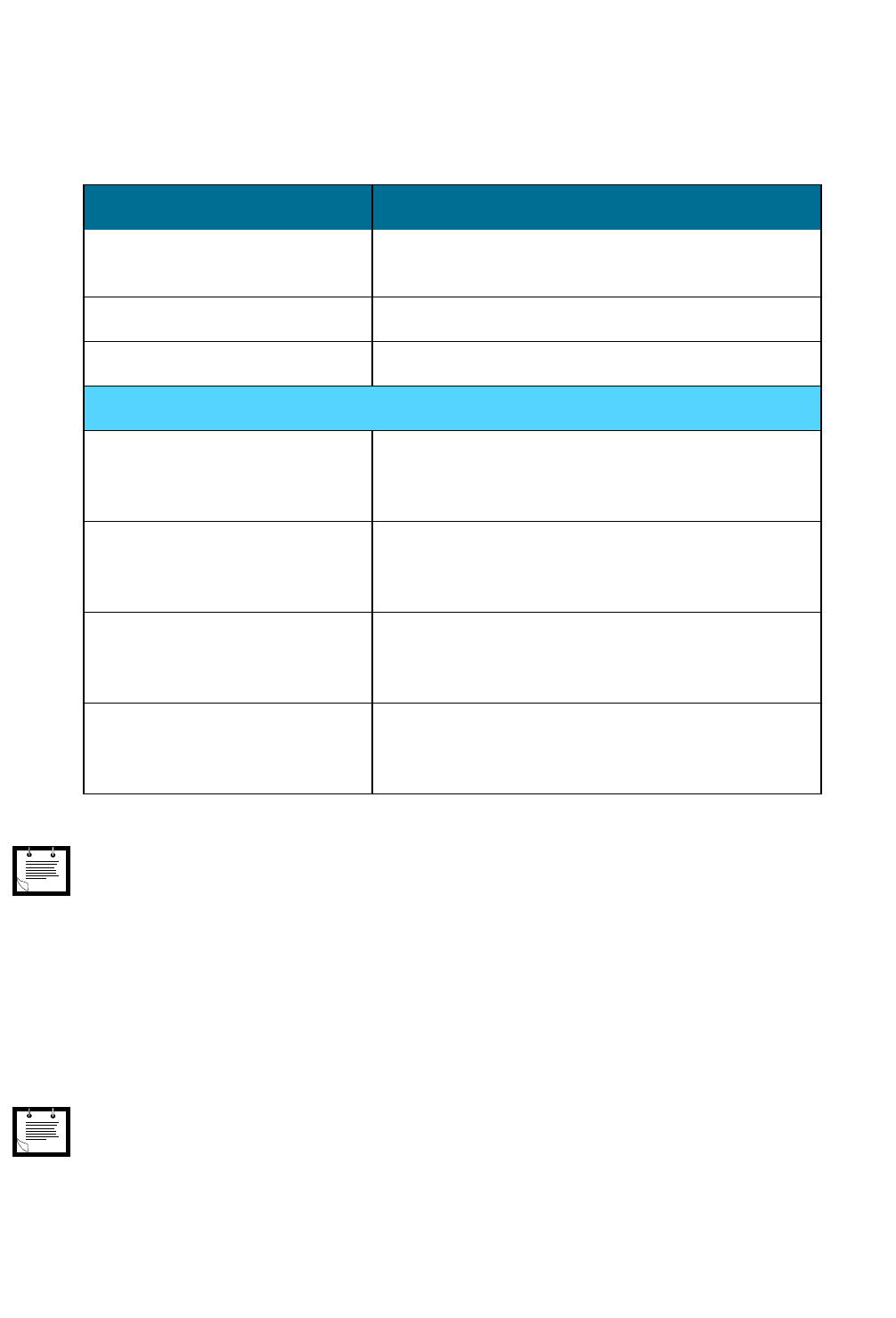
2.2 TERMS AND ABBREVIATIONS
This section provides definitions for terms and acronyms used in this document.
Table 1. Terms and Abbreviations
Acronym/Term Definition/Description
AOC Advice of Charge
CSD Circuit-switched Data
CTS Clear to Send
DCD Data Carrier Detect
DCE Data Communication Equipment (such as modems)
DCS Digital Cellular System (GSM in the 1800MHz band)
DOC Department of Communications (Canada)
DSP Digital Signal Processor
DSR Data Set Ready
DTE Data Terminal Equipment (such as terminals, PCs and so on)
DTMF Dual-Tone Multi-Frequency
DTR Data Terminal Ready
EGSM Extended Global System for Mobile Communications
EIRP Effective Isotropic Radiated Power
EMC Electromagnetic Compatibility
EOTD Enhanced Observed Time Difference
EPOS Electronic Point of Sale
ERP Effective Radiated Power
8 98-08901C66-G
ESD Electrostatic Discharge
ETSI European Telecommunication Standards Institute
FCC Federal Communications Commission (U.S.)
FTA Full Type Approval
GCF GSM Certification Forum
GPIO General Purpose Input/Output
GPRS General Packet Radio Service
GSM Global System for Mobile Communications
IC Integrated Circuit
LNA Low-noise Amplifier
MMCX Miniature Micro Coax
MO Mobile Originated
MT Mobile Terminated
OEM Original Equipment Manufacturer
PCB Printed Circuit Board
PCM Pulse Code Modulation
PCS Personal Communication System (also known as GSM 1900)
PDA Personal Data Assistant
PDU Packet Data Unit
PLL Phase-locked Loop
PTCRB PCS-1900 Type Certification Review Board (GSM North America)
R&TTE Radio and Telecommunications Terminal Equipment
RMS Root Mean Square
RI Ring Indicator
RTS Request To Send
SAR Specific Absorption Rate
SIM Subscriber Identity Module
SMS Short Message Service
SPI Serial Peripheral Interface
TDMA Time Division Multiple Access
UART Universal Asynchronous Receiver Transmitter
USB Universal Serial Bus
USSD Unstructured Supplementary Services Data
VCC Voltage Common Collector
VSWR Voltage Standing Wave Ratio
Table 1. Terms and Abbreviations (Continued)
Acronym/Term Definition/Description
98-08901C66-G 9
2.3 PRODUCT SPECIFICATIONS
Table 2. Product Specifications
Product Features
Operating systems: EGSM: 900/1800 MHz
GSM: 850/1900 MHz
Physical Characteristics
Size (F3003 - F3004): 45.2 x 24.4 x 6.7 mm height refer to the distance
between the customer's board and the g20 top
level
Size (F3012 - F3013): 45.2 x 24.4 x 6.2 mm height refer to the distance
between the customer's board and the g20 top
level
Mounting: Two
Ø2.4 mm holes
Weight: 11.9 grams
Environmental
Operational temperature: -20°C +70°C
Functional temperature: -30°C +85°C
Storage temperature: -40°C +85°C
Performance
Operating voltage: Voltage: 3.0 - 4.2 V
Current consumption: < 2.5 mA @ DRX9 (Idle mode)
Tx power: • 0.8 W, 850 MHz
• 2 W, 900 MHz
• 1 W, 1800/1900 MHz
Interfaces
Connectors: • Single 70-pin, board-to-board
•RF MMCX
SIM Card: • Local SIM connectivity
•32K SIM
• 1.8/3.0 V
Serial: • RS232:
• BR from 300 bps to 115 Kbps
• Auto BR from 300 bps to 115 Kbps
•USB
• 12 Mbps USB specifications, Rev. 1.1
Data Features
GPRS: • Multi-slot class 8 (4 down; 1 up)
• Max BR 85.6 Kbps
• Class B GSM 07.10 multiplexing protocol
• Coding scheme CS1-CS4
CSD: Max BR 14.4 Kbps
SMS: • MO/MT Text and PDU modes
• Cell broadcast
FAX Class 1
10 98-08901C66-G
Voice Features
Telephony
Digital audio
Differential analog audio lines
Vocoders EFR/ER/FR/AMR
DTMF support
Audio control: echo cancellation, noise suppression, side tone and gain control
GSM Supplementary Service
USSD Phase II
Call forwarding
Call hold, waiting and multiparty
Call diverting
Missed-call indicator
AOC
Call barring
Character Set
UTF8
UCS2
Control/Status Indicators
GPRS coverage
Wakeup
TX enable
Reset
Antenna Detect
Features over RS232
Embedded TCP/IP stack
STK Class II
Emergency and Location
FCC E911 Phase II Location Mandate using EOTD
AT Command Set
GSM 07.05
GSM 07.07
Motorola proprietary AT commands
Accessories
Firmware data loader
Data logger
Developer Kit
Note
Specifications are subject to change without prior notice.
Table 2. Product Specifications (Continued)

98-08901C66-G 11
2.4 MODELS DESCRIPTION
Table 3 lists the available g20 models.
2.5 REGULATORY APPROVALS
The following regulatory approvals apply for the g20 module:
•FCC
• DOC
• PTCRB
•R&TTE
•EMC
•GCF
2.6 REGULATORY REQUIREMENTS
The Federal Communications Commission (FEC) requires application for certification of digital devices in accordance with
CFR Title 47, Part 2 and Part 15. This includes Electromagnetic Energy Exposure (EME) testing. As the g20 modem is not a
standalone transceiver but is an integrated module, the g20 cannot be tested by itself for EME certification. It is, however, the
integrator’s responsibility to have the completed device tested for EME certification.
2.7 REGULATORY STATEMENT
The following safety precautions must be observed during all phases of the operation, usage, service or repair of any cellular
terminal or mobile incorporating the g20 module. Manufacturers of the cellular terminal are advised to convey the following
safety information to users and operating personnel, and to incorporate these guidelines into all manuals supplied with the prod-
uct. Failure to comply with these precautions violates safety standards of design, manufacture and intended use of the product.
Motorola assumes no liability for customer failure to comply with these precautions.
13. The g20 must be operated at the voltages described in the technical documentation.
14. The g20 must not be mechanically nor electrically changed. Use of connectors should follow the guidance of the technical
documentation.
15. The g20 is designed the meet the EMC requirements of ETS 300 342.
16. When integrating the g20 into a system, Motorola recommends testing the system to ETS300342-1.
17. The g20 meets the safety requirements of EN60950.
18. Systems using the g20 are subject to mandatory EMC testing under directive 89/336/EEC (see item 3 above). Other
directives, such as the LVD directive 73/23/EE, may also apply to a system using the g20 module.
Table 3. g20 Models
Model Operating
Bands Interface Connectors Serial Interface
F3003 GSM 850/1900 • 70-pin 3 mm stacking height connector
• MMCX RF connector USB/RS232
F3004 EGSM 900/1800 • 70-pin 3 mm stacking height connector
• MMCX RF connector USB/RS232

12 98-08901C66-G
2.8 SAFETY PRECAUTIONS
2.8.1 User Operation
Do not operate your unit when a person is within 8 inches (20 centimeters) of the antenna. A person or object within 8 inches
(20 centimeters) of the antenna could impair call quality and may cause the phone to operate at a higher power level than neces-
sary.
IMPORTANT: The unit must be installed in a manner that provides a minimum separation distance of
20 cm or more between the antenna and persons to satisfy FCC RF exposure requirements for mobile transmitting devices.
IMPORTANT: To comply with the FCC RF exposure limits and satisfy the categorical exclusion requirements for mobile
transmitters, the following requirements must be met:
2.8.2 Antenna Installation
• The antenna installation must provide a minimum separation distance of 20 cm from users and nearby persons and must not
be co-located or operating in conjunction with any other antenna or transmitter.
• The combined cable loss and antenna gain must not exceed +9.9 dBi and total system output must not exceed 1.5 W ERP
(Cellular) / 3.0 W EIRP (PCS) to qualify for categorical exclusion requirements of 2.1091. OEM installers must be provided
with antenna installation instruction and transmitter operating conditions for satisfying RF exposure compliance.
98-08901C66-G 13
3. HARDWARE DESCRIPTION
3.1 G20 BLOCK DIAGRAM DESCRIPTION AND OPERATION OVERVIEW
This chapter describes the basic blocks comprising the g20 module and the connectivity options for the module.
3.1.1 g20 Block Diagram
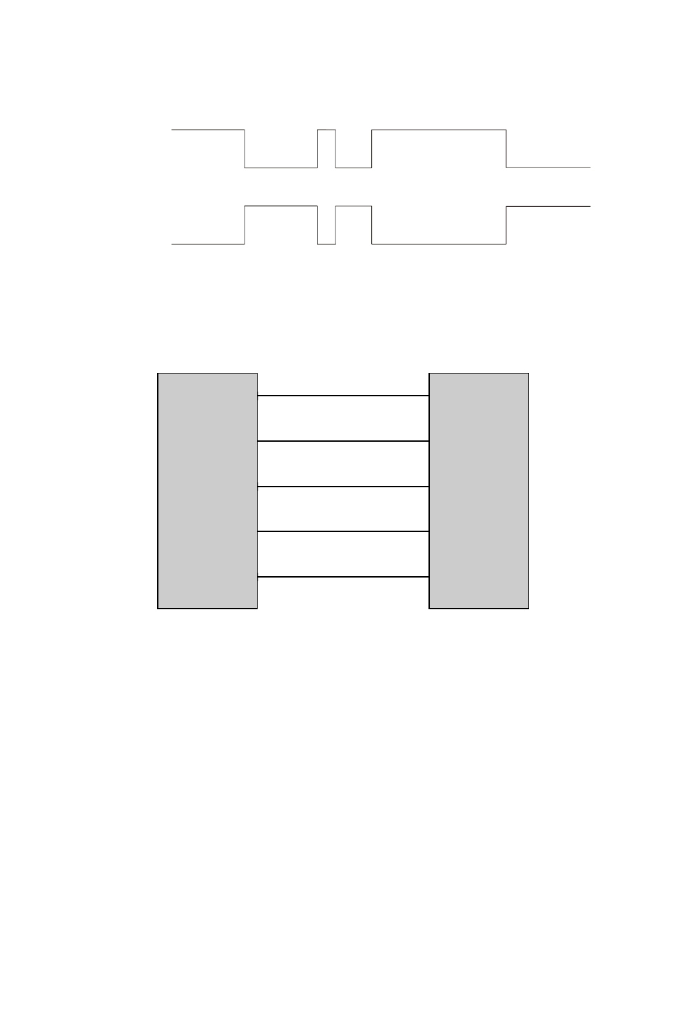
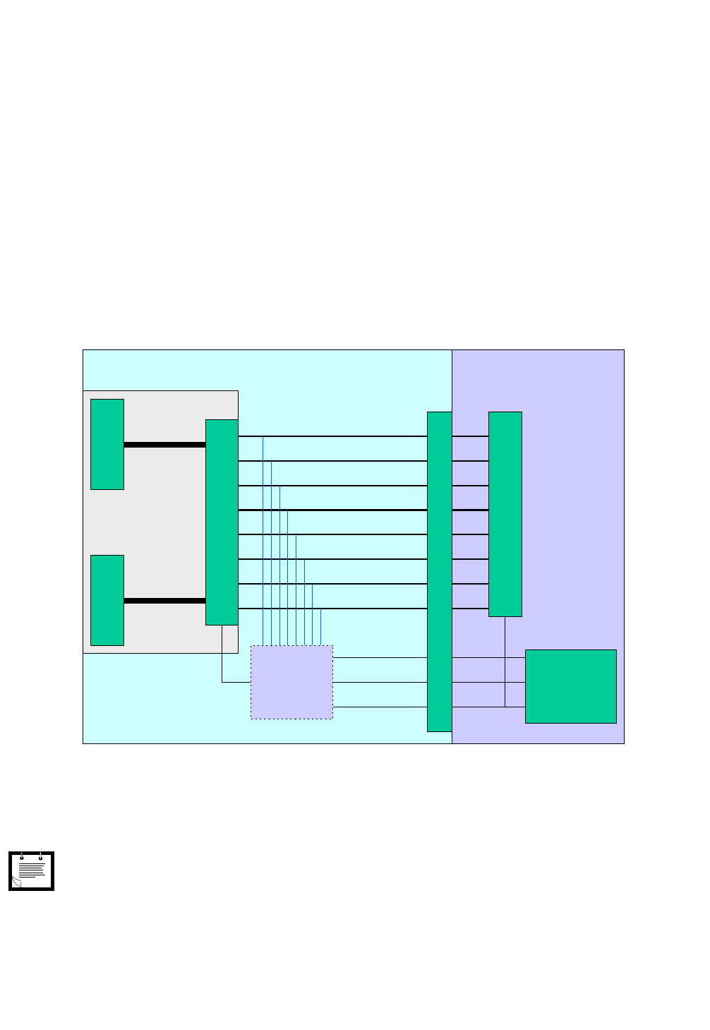
Figure 1 shows a block diagram for the g20 module:
Figure 1. g20 Block Diagram
The g20 consists of the following blocks:
•Power and Audio Management IC: This block is responsible for the power on/off process, analog audio drivers, internal
regulators, realtime clock activities, and the battery charging process. When an On command is received, this IC wakes up
the internal regulators and controls the reset process. This activity turns the unit on. When an Off command is received, this
IC sends the request to the main processor, which in turn shuts down the unit in an orderly fashion. During shutdown, the
unit is disconnected from the network, all tasks are terminated and the regulators are shut down. The on/off inputs (On/Off
and Ignition) are always on, even when the unit is off.
Main
Processor
&
DSP
Memories
Power &
Audio
Management
IC
Receiver
IC
Control
USB
Driver
PCM
SIM
GPIO
Interface Connector
SPI
ADC
Audio
Charger
Power
On/Off/IGN
g20
Transmitter
IC
Ant
Serial

14 98-08901C66-G
•Main Processor and DSP: This block is responsible for all the main tasks in the unit. It contains the following components:
• Main processor
• DSP for controlling speech options
• UART
• USB block
• Digital audio driver
• SIM card
• Two SPI buses (one internal and one externally accessible)
• Main clock (26 MHz)
• Address/data buses
• RF PLL
• Controller to the RF ICs, which is the heart of the unit
This module provides the following connectivity:
• Address/data bus
• UART to the user connector
• USB via a USB driver to the user connector
• Digital audio (PCM) to the user connector
• SIM card interface
• SPI to the user connector
• SPI to control the RF ICs
• Control signals to the power amplifier IC
• Handshake with the Power and Audio Management IC
• General I/O to the user connector
•Receiver Block: This block is an RF block that contains all the receiver channels. It contains the following components:
• Front filters
• LNAs
•Mixers
•VCOs
• I/Q outputs
• Control signals
•Transmitter Block: This is an RF block that contains all the transmitter channels. It contains the following components:
• Power amplifiers
• Power control loop
• Antenna switch
• Harmonic filter
• Input buffers
• Control signals
• Antenna connection
98-08901C66-G 15
3.1.2 Basic RS232 and Analog Audio Connectivity
The following basic g20 connectivity requirements apply for UART (RS232) and analog audio connections (see Figure 2 for
reference):
• The RS232 is connected via eight pins to the g20.
• The SIM card is connected via five pins to the SIM driver of the g20.
• The microphone is connected via two pins to the g20 (Mic and Mic Ground).
• The Speaker is connected via two differential lines to the g20.
• The power supply is connected via eight pins (four VCC and four Ground) to the g20.
• The On/Off or Ignition pin is connected.
Figure 2. Basic RS232 and Analog Audio Connectivity
3.1.3 Basic RS232 and Digital Audio Connectivity*
The following basic g20 connectivity requirements apply for UART (RS232) and digital audio connections (see Figure 3 for
reference):
• The RS232 is connected via eight pins to the g20.
• The SIM card socket is connected via five pins to the SIM driver of the g20.
• The DTE DSP is connected via four pins to the g20 (PCM).
• The power supply is connected via eight pins (four VCC and four Ground) to the g20.
• The On/Off or Ignition pin is connected.
* Support for this feature depends on the current g20 release.
Main
Processor
&
DSP
Memories
Power &
Audio
Management
IC
Receiver
IC
Power
Supply
On/Off or
Ignition
SPKR
Mic
SIM
Socket
DTE
UART
Control
USB
Driver
PCM
SIM
GPIO
Interface Connector
SPI
ADC
Audio
Charger
Power
On/Off - IGN
g20
Transmitter
IC
Ant
Serial
16 98-08901C66-G
Figure 3. Basic RS232 and Digital Audio Connectivity
3.1.4 Additional Recommended Connections
Additional g20 connectivity options are described below (see Figure 4 for reference):
• A USB connector that is connected via three lines to the g20. In this case, when USB is used, the DTE UART should be in
tri-state (high impedance).
• An SPI block that is connected via five pins to the g20 (for debug accessibility).
Figure 4. Additional g20 Connectivity
Main
Processor
&
DSP
Memories
Power &
Audio
Management
IC
Receiver
IC
Power
Supply
On/Off or
Ignition
SIM
Socket
DTE
DSP
DTE
UART
Control
USB
Driver
PCM
SIM
GPIO
Interface Connector
SPI
ADC
Audio
Charger
Power
On/Off - IGN
g20
Transmitter
IC
Ant
Serial
Main
Processor
&
DSP
Memories
Power &
Audio
Management
IC
Receiver
IC
USB
Connector
SPI
Device
Control
USB
Driver
PCM
SIM
GPIO
Interface Connector
SPI
ADC
Audio
Charger
Power
g20
Transmitter
IC
Ant
Serial
98-08901C66-G 17
3.2 POWER SUPPLY AND CURRENT CONSUMPTION
This section describes the following power-related considerations for the g20:
• Power supply design
• g20 current consumption
• Turning the unit on/off
• Sleep mode options
3.2.1 Power Supply Design
The following power supply design considerations apply to the g20:
• The g20 is designed to operate between 3.0 V to 4.2 V on the g20 input (after all losses). In order to reduce battery power
consumption, it is important to verify power supply line and regulator losses in the PCB.
• The g20 is a GSM/GPRS phone that transmits in 0.5 ms pulses every 4.6 ms. The peak current is approximately 2.0 A.
• When the power supply is lower than 2.85 V, the g20 software determines that the battery is low and disconnects the unit.
• When the voltage is greater than 4.25 V, the g20 software detects an over voltage condition and does not allow the unit to
establish a call.
• The VCC line typically drops during TX periods.
Figure 5. VCC Signal During TX Periods
To minimize the ∆, it is recommended to use lines that are as short as possible, and to place a 1000uF capacitor (or the maximum
possible) in the g20 VCC input. (When a battery is used, there is no need for a large capacitor.)
It is recommended to keep the ∆ less than 0.3 V.
3.2.1.1 Power Supply RF Filtering
It is recommended to add RF filtering to the DC lines.
Use 100nF, 39pF, 22pF or 8.2pF capacitors in parallel to the power supply lines (close to the g20 connector). The following
capacitor requirements apply:
• 100nF is for filtering logic data noise (clocks, serial communications, and so on).
• 39pF is used for 850/900 bands.
• 22pF is used for 900 band.
• 8.2pF is used for 1800/1900 bands.
The appropriate capacitor value(s) should be selected according to the GSM band used by the customer.
Note
The power supply should be able to drive at least 2.5 A at 3 V DC.
Transmit
Periods
VCC
TX TX TX
18 98-08901C66-G
3.2.2 g20 Current Consumption
In order to design the power supply correctly and to calculate the battery life, you should take into account the current
consumption of the g20 when operating in different modes.
3.2.3 Turning the Unit On/Off
Two different mechanisms are available to turn the g20 on and off:
• On/Off signal (Pin 53)
• Ignition signal (Pin 51)
Table 4. g20 Current Consumption
Mode Current Consumption (mA RMS)
g20 in Sleep mode (camped and
Sleep-mode enabled)
< 2.5 mA, RMS @ DRX9, Typical 2.2 mA
< 4.5 mA, RMS @ DRX2, Typical 3.5 mA
g20 during search time < 40 mA, RMS, Typical 25 mA, RMS
g20 off < 100 uA – Typical 25 uA
g20 during a call
GSM 900 @ Power level #5 < 350 mA, Typical 270 mA
@ Power level #10, Typical 160 mA
@ Power level #19, Typical 135 mA
GSM 850 @ Power level #7 < 250 mA, Typical 185 mA
@ Power level #10, Typical 160 mA
@ Power level #19, Typical 135 mA
DCS 1800 @ Power level #0 < 300 mA, Typical 220 mA
@ Power level #10, Typical 160 mA
@ Power level #19, Typical 135 mA
PCS 1900 @ Power level #5 < 300 mA, Typical 240 mA
@ Power level #10, Typical 160 mA
@ Power level #19, Typical 135 mA
Note
DRX2/9 is the rate used by the base station to query the mobile station. The network operator sets this parameter.
Note
The g20 power-on and power-off timing may vary slightly, depending on the software version.

98-08901C66-G 19
3.2.3.1 On/Off Signal
The on/off signal is an active-low toggle switch. After power is applied to the g20, the on/off signal is pulled high to VCC by
an internal 200KΩ resistor.
To turn the g20 on, the on/off signal should be pulled low for a minimum of 800 ms (T1). This will initiate the power-on process,
which lasts about five seconds, after which the g20 is ready to communicate.
To turn the g20 off, the on/off signal should be pulled low for a minimum of two seconds. This will initiate the power-off
process, which lasts about eight seconds, after which the g20 will shut down. The g20 can be turned off only if at least 10 seconds
have elapsed since the last power on.
Figure 6 shows the timing diagram for the on/off signal.
Figure 6. On/Off Signal Timing Diagram
In Figure 6, the following timing requirements apply:
• T1 minimum = 800 ms.
• T2 minimum = 10 seconds.
• T3 minimum = 2 seconds.
3.2.3.2 Ignition Signal
The ignition signal turns the g20 on and off, depending on its logic state.
To turn the g20 on, the ignition signal must be pulled high. This initiates the power-on process, which lasts about five seconds,
after which the g20 is ready to communicate. The g20 remains active for the duration of the ignition signal remaining high.
To turn the g20 off, the ignition signal must be pulled low. This initiates the power-off process, which may last up to 30 seconds,
after which the g20 will shut down. The ignition signal must remain low for the duration of the power-off process, until the g20
shuts down. Otherwise, the power-off process may be interrupted or may not complete.
3.2.4 Sleep Mode Options
This section describes how the g20 can be awakened by the DTE and vice-versa.
The DCE (g20) and the DTE can incorporate a sleep mechanism in their application in order to conserve battery life.
Sleep mode enables the g20 to be awakened when the DTE wants to communicate with it. Conversely, it also enables the DTE
to be awakened by the g20 when the g20 wants to communicate with it. The g20 will not enter sleep mode if the USB is
connected.
3.2.4.1 General
• The g20 Sleep Mode option can be enabled or disabled using ATS24.
• Sleep mode is activated by sending ATS24 = n, where n = 1, 2, 3 or 4 seconds. (To disable Sleep mode, send ATS24=0.)
• The g20 drops the CTS (h/w Flow Control) when it is in Sleep mode.
• The g20 does not enter Sleep mode when data is present on TXD or RXD lines.
• At the end of the TXD (meaning, the TXD buffer is empty), the g20 waits n seconds (as defined in ATS24 = n) before enter-
ing Sleep mode.
T1 T2 T3
20 98-08901C66-G
• The DTE uses CTS to send data only when the g20 is awake. The DTE waits when the g20 is in Sleep mode.
• When the g20 is asleep, the CTS line will blink.
• The DTE should drop RTS during the sleep period in order to prevent the loss of data sent by the g20.
Figure 7. CTS Sleep Mode Timing
3.2.4.2 DCE/DTE Connectivity
Figure 8 shows DCE/DTE connectivity:
Figure 8. DCE/DTE Connectivity
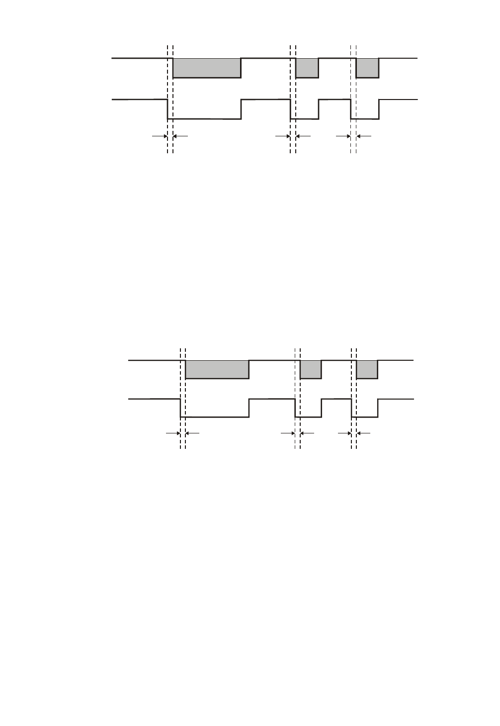
Waking Up the g20:
The following apply when waking up the g20:
• The Wake-up In line is used to awaken the g20. This input is routed into an Interrupt in the g20.
• Whenever the Wake-up In line is at logic “low”, the g20 remains in an awake state.
• When the DTE needs to send data, it should activate this line, wait 30 ms (the wake time required for the g20), and then start
sending the data.
Inactive
Sleep
Inactive
Sleep
Active
Awake
Active
Awake
g20 Sleep Periods
CTS
g20
(DCE)
User
UART
(DTE)
RTS
CTS
TXD
Wake-up Out
Wake-up In
9
15
21
26
16
98-08901C66-G 21
• While the DTE is sending data, the wake-up line should remain low, so that the g20 does not enter Sleep mode.
Figure 9. Waking Up the g20 when the DTE wants to Send Data
Waking Up the DTE:
The following apply when waking up the DTE:
• The g20 uses the Wake-up Out line to indicate to the DTE that data is present.
• The DTE should not enter Sleep mode when the Wake-up Out line is low.
• When the g20 has data to send to the DTE, it drops the Wake-up Out line to low.
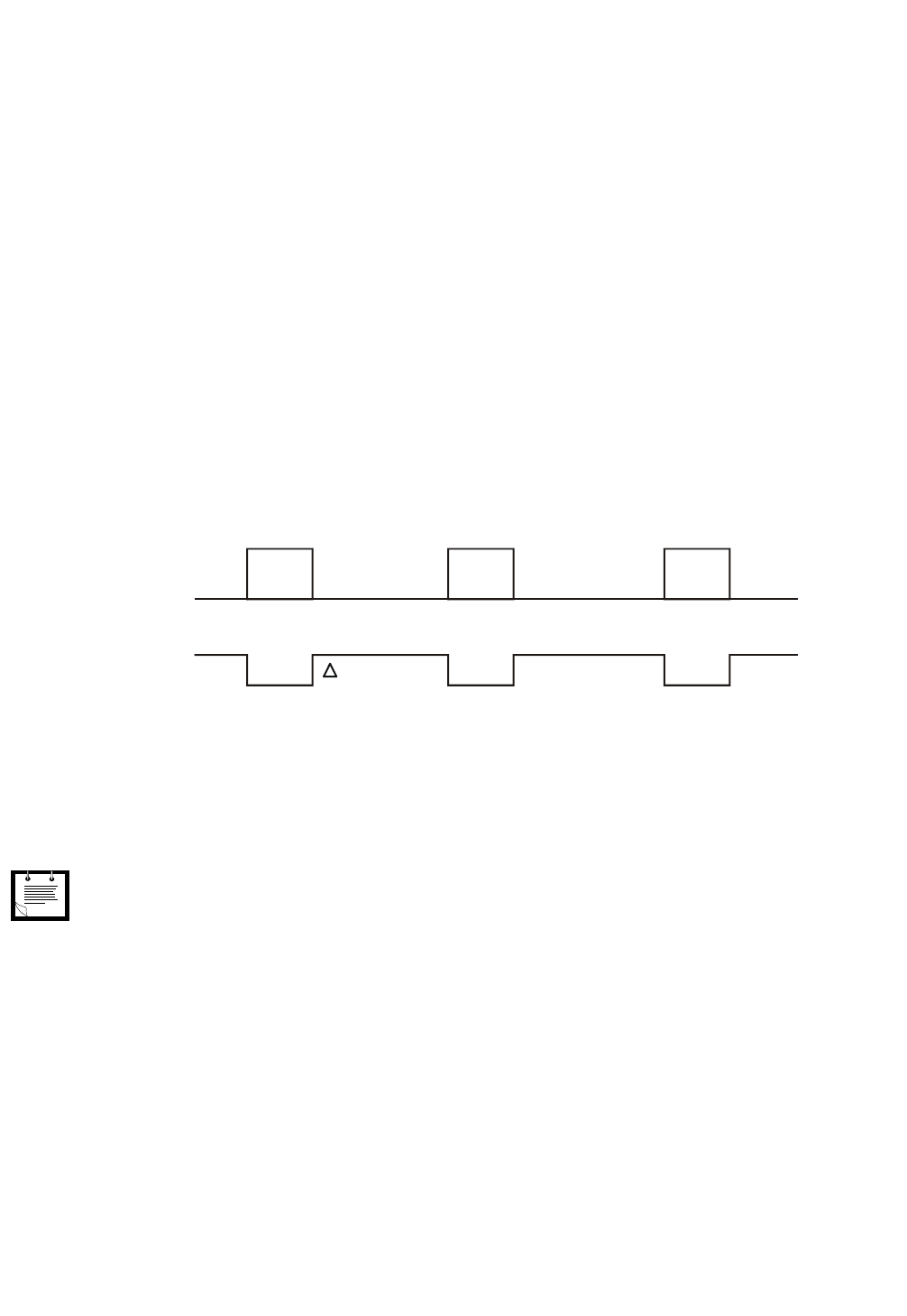
• The g20 will send the Wake-up Out line #ms to low, as indicated by S102 in Figure 10.
• While the g20 is sending data, the Wake-up Out line remains low.
• After the sending of data is completed, the g20 brings the Wake-up Out line to high.
• The DTE should keep RTS off during this sleep period in order to avoid sending data when it is not ready.
Figure 10. Waking Up the DTE when the g20 wants to Send Data
3.3 COMMUNICATION INTERFACES
This section describes the following four interfaces that are available in the g20:
• RS232
•USB
•SIM
•SPI
DTE TXD
Wake-up
In line
30 ms 30 ms 30 ms
RXD
Wake-up
Out line
S102 ms S102 ms S102 ms
22 98-08901C66-G
3.3.1 RS232
The following apply when using the RS2332 interface of the g20:
• The g20 supports full hardware flow control (8 pins), software flow control (Xon/Xoff) and non-flow control.
• The g20 UART is connected directly to the interface connector.
• The g20 is a DCE device. Applicable line terminology is shown in Figure 11.
Figure 11. g20 RS232 Interface
3.3.1.1 RS232 Levels
RS232 levels are as follows:
• Vih = 1.95 V minimum, 3.0 V maximum
• Vil = 0.8 V maximum
• Voh = 2.56 V minimum @ 100 uA
• Vol = 0.2 V maximum @ 100 uA
3.3.1.2 RS232 Connection
As shown in Figure 12, the g20 can be connected to the DTE UART using all eight RS232 signals.
The g20 selects its communication channel, RS232 or USB, depending on the state of the USB_VBUS signal (pin 10) at power
up. The g20 operates in RS232 mode if the USB_VBUS signal is low at power up and remains low during operation.
The g20 does not support dynamic switching between RS232 and USB channels during operation, and does not support
simultaneous operation.
Note
A buffer is required whenever DTE levels do not match g20 levels (not 5V tolerant).
Note
When the g20 is switched off, it is recommended to keep the RS232 signals of the DTE at tri-state or at a low level
in order to prevent potential latch-up.
g20
(DCE)
User
UART
(DTE)
TXD
RXD
RTS
CTS
DTR
DSR
DCD
RI
21
11
9
15
19
13
17
23
98-08901C66-G 23
3.3.2 USB
The g20 selects its communication channel, RS232 or USB, depending on the state of the USB_VBUS signal (pin 10) at power
up. The g20 operates in USB mode if the USB_VBUS signal is high at power up and remains high during operation. The
USB_VBUS signal is the power line of the USB interface, which powers the USB circuitry.
The g20 does not support dynamic switching between RS232 and USB channels during operation, and does not support
simultaneous operation
When USB is used, the DTE device must unload (meaning disconnect or place in tri-state) the RS232 lines. Otherwise, the USB
may not operate properly.
The USB port is also used to load software into the g20. It is recommended to include connectivity to this port in the user
application.
The g20 supports USB 1.1 at a baud rate of 12 Mbps.
3.3.2.1 USB Connection
A USB connection diagram is shown in Figure 12.
Figure 12. g20 USB Connection for g20 Models
As shown in Figure 12, the g20 USB is connected via three lines to the USB connector in the user application: D+, D- and USB
VBUS. When USB VBUS is applied, the g20 detects it and switches the main processor to USB mode.
Note
The DTE UART loads the USB driver/main processor lines. Therefore, the UART should be kept in tri-state.
USB usage eliminates sleep mode in the g20.
g20 Main
Processor
USB
Driver
D+
D-
USB VBUS
USB
Detect
TXD
RXD
RTS
CTS
DTR
DSR
DCD
RI
USB
Connector
3 state
g20 DTE
U
A
R
T
U
S
B
M
U
X
D
T
E
U
A
R
T
21
11
9
15
19
13
17
23
12
14
10
24 98-08901C66-G
3.3.3 SIM
The g20 includes a SIM card driver, however, it does not contain a SIM socket. SIM signals are routed to the interface connector
and include all the functionality required for SIM card operation. The SIM card socket must be located in the customer
application, and connected to the g20 interface connector as described in the following section.
3.3.3.1 SIM Connection
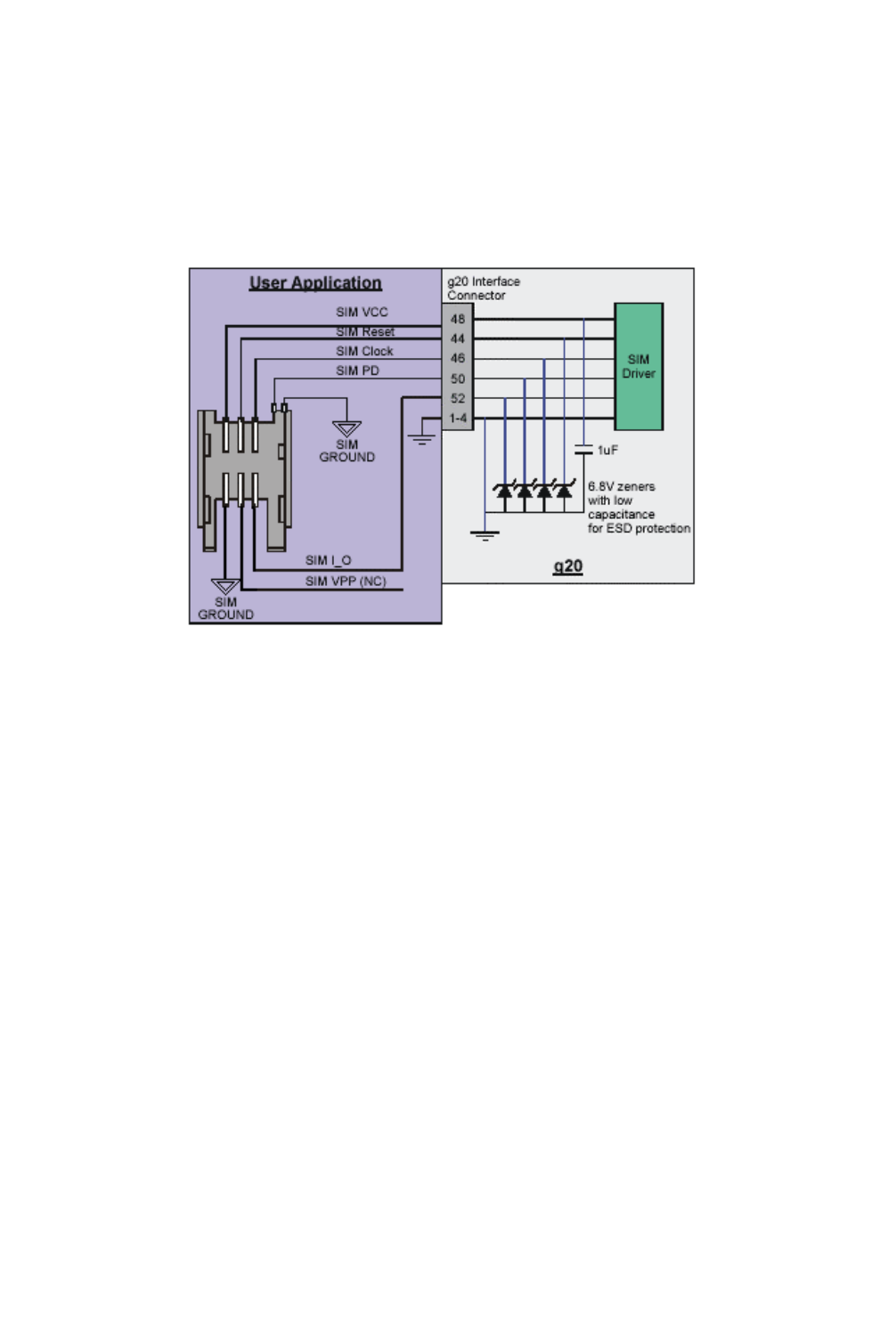
Figure 13 shows a g20 SIM connection:
Figure 13. g20 SIM Connection
The following apply for g20 SIM connections:
• The g20 passes all ETSI tests when an external socket is connected to the g20 with lines shorter than 10 cm. Longer signal
connections may require additional testing to be performed.
• The g20 supports 3.0V and 1.8V SIM cards.
• The SIM card detect signal, SIM_PD, operates in active low logic.
The SIM card signals must be carefully routed to minimize ESD and EMI susceptibility. The following are guidelines for proper
SIM application operation:
• The SIM ground must be connected to the main ground through an inductive element.
• The SIM card socket should be located away from the antenna as far as possible.
• The SIM logic signals, DIO, CLK, RST and PD, may need to be filtered with 10pF capacitors, depending on the application
and its distance from the antenna.
• The SIM detect signal, SIM_PD, should be connected to the g20 through a 15uH inductor.
• Low capacitance zener diodes should be placed as close as possible to the SIM card socket contacts, for proper ESD
protection.
98-08901C66-G 25
3.3.4 SPI
The SPI is a standard microprocessor bus used as a g20 debugging port. This port activates a debug option that enables logs to
be taken from the g20 while it is operating. It is recommended that this bus be accessible in the user application. In the g20
Developer’s Kit, the SPI bus is converted to an RS232 protocol using a special interface circuit. It then uses the standard RS232
port for debugging. Table 5 shows the pins available on the SPI bus.
3.3.4.1 SPI Connection
3.3.5 Unique g20 Interfaces
The g20 contains unique functions (pins) that may be required by selected user applications, such as TX_EN, Antenna Detect,
GPRS Detect and Entertainment Mute. Each of these functions is described in the sections that follow.
3.3.5.1 Transmit Enable
This pin indicates when the g20 is transmitting RF in the antenna.
Figure 14. TX_EN Transmission
3.3.5.2 GPRS Coverage Indication
This pin indicates whether or not the g20 is located in an area with GPRS network coverage. This pin can be used to indicate
the GPRS coverage status before GPRS section activation has occurred, or before a switch to circuit-switched data is made. The
default operation of this signal is active low, meaning this signal is at 0 when GPRS coverage is available. It is possible to switch
the signal’s polarity to active high using an AT command. Refer to the g20 AT Commands document (9808901C68-O) for the
AT commands description.
Table 5. SPI Pinout
Pin # Name Function Input/Output
70 SPI_CS SPI chip-select Output
62 SPI_IRQ_N SPI Interrupt Input
64 SPI_DIN SPI MISO input Input
68 SPI_DOUT SPI MOSI output Output
66 SPI_CLK SPI clock Output
RF TransmissionNo RF Transmitted No RF Transmitted

26 98-08901C66-G
3.3.5.3 Antenna Detect
This pin indicates whether or not the antenna is inserted. This option can be used with antennas with a resistance to ground of
less than 100K. The antenna detect circuit detects whether the ohmic resistance of the antenna is 100 Kohm or lower, which is
required for the antenna to be detected. If the ohmic resistance is higher than 100 Kohm, the antenna is not detected.
In software versions 34D and later, this signal has been collaborated to match the logic detection threshold of the g20, and
exhibits best results when connected back to the g20. A dedicated g20 input signal, pin 37, is available for the antenna detection
input. This is to ensure proper operation of the antenna-detect AT command, which enables software indication of the antenna
state.
Figure 15. Antenna Detect
3.4 AUDIO INTERFACES
The g20 has an analog audio interface and a digital audio interface. Both of these interfaces are described in the sections that
follow.
3.4.1 Analog Audio Interfaces
The g20 supports microphone input, headset microphone input, differential speaker output, and a differential alert speaker.
3.4.1.1 Analog Input
The g20 has two different analog inputs, referenced to the microphone ground (pin 59). The g20 contains an analog amplifier
with a default gain of 16dB, which can be adjusted in seven steps between 0 and 31dB using the AT+MMICG command. For
more details about this command, refer to the g20 AT Commands document (9808901C68).
When the default gain of 16dB is used, then the level considerations should be as follows:
•Headset microphone: Pin 57 is the headset microphone input. The input for this line can come directly from a headset
microphone. In order for the headset microphone to be active, the headset interrupt signal (pin 55) needs to be pulled low.
The maximum input to the g20 headset microphone before there is signal distortion in the network is 12 mvRMS.
•Hands-free microphone: Pin 61 is the microphone input to the g20. When the headset interrupt signal is not pulled low,
this microphone will be active. The maximum input to the g20 microphone before there is signal distortion in the network is
32 mvRMS.
3.4.1.2 Analog Output
The g20 has a differential speaker output and an alert output:
•Speaker output: When headset mode is used, the headset speaker should be connected to the SPKR_N signal of the g20.
When a differential amplifier is used, both lines should be connected. An 8-ohm speaker can be connected directly to the
speaker lines.
•Alert: The g20 supports a direct connection for an alert transducer, in order to build a handset from the g20. All the sounds
that are transmitted to the alert can be routed to the speaker using the appropriate AT command.
Antenna DetectedAntenna Not Detected
98-08901C66-G 27
Table 6 shows the SPKR_N output in headset mode for different network signal levels when the g20 is set to the maximum
volume level and the headset interrupt is pulled low.
The measurements shown in Table 6 apply in the following configuration:
Figure 16. Headset Speaker Output Measurement Configuration
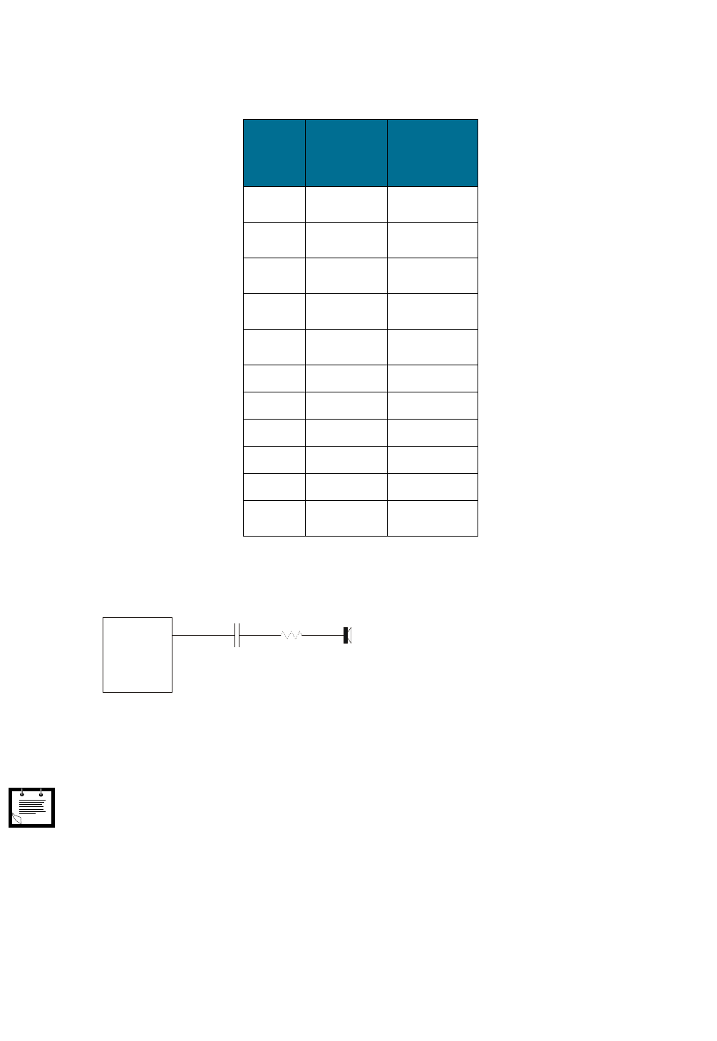
Table 6. Headset Speaker Output at Maximum Volume Level
dBm0 mV RMS
Headset
Speaker
(mV RMS)
3.14 1111.9 174
0 774.6 165
-5 435.6 132
-10 244.9 72
-15.5 130 39
-16 122.8 36
-17 109.4 32
-20 77.5 24
-25 43.6 5
-30 24.5 4
max 3000 210
Note
The series resistor value must be at least twice the impedance of the connected headset speaker.
68 ohm10uf
SPKR_N
g20
Headset
28 98-08901C66-G
Table 7 shows the output of the SPKR_N signal for different network signal levels when the g20 is set at the maximum volume
level and the headset interrupt is not pulled low.
Table 8 shows the SPKR_N output at different volume levels, when a 500mV RMS signal is transmitted from the network.
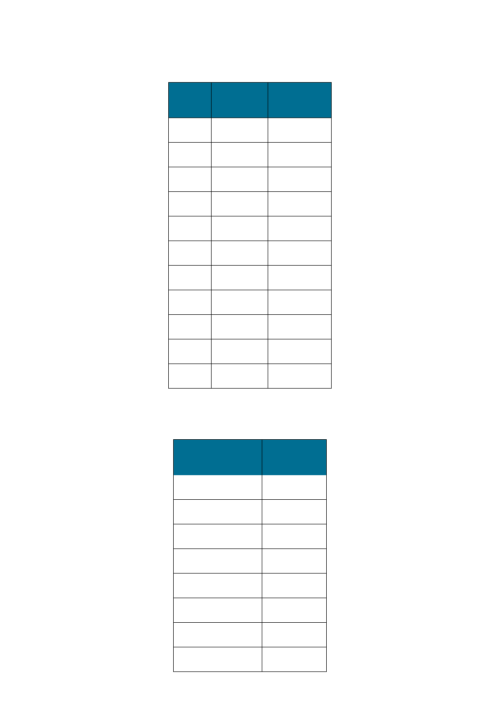
Table 7. SPKR_N Output in Speaker Mode at Maximum Volume Level
dBm0 mV RMS SPKR_N
(mV RMS)
3.14 1111.9 374
0 774.6 267
-5 435.6 148
-10 244.9 83
-15.5 130 45
-16 122.8 42
-17 109.4 37
-20 77.5 26
-25 43.6 14
-30 24.5 7
max 2600 900
Table 8. SPKR_N Output when a 500mV RMS Signal is Transmitted
Handset Volume SPKR_N
(mV RMS)
0 (lowest gain) 16
122
231
343
461
587
6120
7 (highest gain) 170
98-08901C66-G 29
Table 9 shows the typical keypad tone levels generated by the g20. These measurements taken with the g20 in handset mode
(meaning the headset-detect signal is not pulled low).
Table 10 shows the keypad tone levels generated by the g20 when in headset mode (meaning the headset-detect signal is pulled
low).
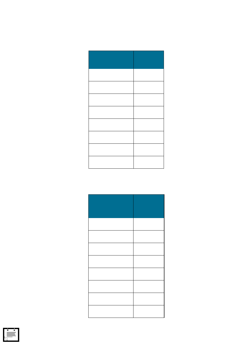
Table 9. SPKR_N Output when g20 is in Handset Mode
Handset Volume SPKR_N
(mV RMS)
00
1122
2172
3244
4342
5482
6678
7954
Table 10. Headset Speaker Output
Headset Volume
Headset
Speaker
(mV RMS)
00
14
25.5
37.5
4 10.5
514
6 19.5
7 27.5
Note
The above measurements apply to the configuration shown in Figure 16.
30 98-08901C66-G
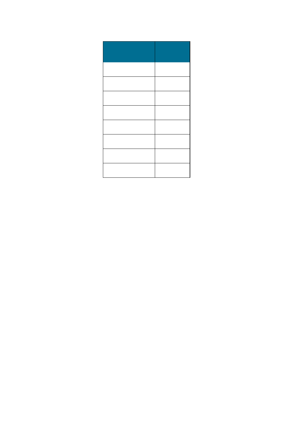
Table 11 shows the levels of the alert transducer measured on the ALERT_P signal at different ring volumes.
3.4.1.3 Audio Circuit Design Considerations
In order to design an audio circuit that produces clear audio, without being affected by the GSM transmission, the following
guidelines should be considered when designing the circuit:
• The audio input to the g20 should be referenced to the MIC_GND line of the g20.
• The microphone bias of the g20 for both the microphone and headset is 2.2 V. If a microphone with a different voltage is
used, the bias should be as clean as possible, and referenced to MIC_GND. Because most GSM buzz (217Hz TDMA noise)
is generated from the microphone path, if a different bias is created, it should be filtered to supply DC only.
• The MIC_GND and GND are connected inside the g20 and should not be connected to the application board.
• Keep the lines of the microphone inputs as short as possible. To filter the lines from RF emission, 39pF capacitors can be
used.
• The g20 GND should be connected on all four pins, with two mounting screws to the application ground.
• If possible, the RF cable ground from the g20 should be connected to the GND of the g20.
• The digital lines of the application should never be referenced to the MIC_GND.
3.4.2 Digital Audio Interface
The g20 digital audio interface is a full-duplex SAP (serial audio port) comprised of four signals:
•PCM_FS: This pin is used for frame sync output provided by the g20.
•PCM_CLK: This pin is used for the clock output provided by the g20.
•PCM_DIN: This pin is the serial input to the g20 SAP.
•PCM_DOUT: This pin is the serial output of the g20 SAP.
Table 11. Alert Transducer Levels for the ALERT_P Signal
Handset Volume ALRT_P
(mV RMS)
087
1124
2175
3250
4350
5487
6680
7980
98-08901C66-G 31
The following conditions apply to the digital audio interface of the g20:
• The g20 SAP works in network mode, with four slots in each frame. Each slot consists of 16-bit data.
• The g20 sends and receives data on the first slot only.
• The frame sync rate is 8 KHz, and the clock rate is 512 KHz.
• The g20 is the master in the SAP network. Therefore, the connected DSP should be configured as a slave.
• Digital audio lines should be connected to Codex or DSP on the application side.
3.5 ANTENNA
The g20 has two models, one for North America Frequency bands (850/1900 MHz), and one for European Bands
(900/1800 MHz). The following connection requirements apply for the g20 antenna:
• The g20 is terminated with an MMCX connector, and with 50-ohm impedance in the relevant frequencies.
• The g20 can be connected to any antenna with 50-ohm impedance in the relevant frequency bands.
• The g20 is designed to work on VSWR, up to 2:5:1 The antenna should meet this requirement.
3.5.1 Antenna Performance Recommendations
Table 12 lists the performance recommendations for the g20 antenna.
3.6 ESD PROTECTION
In general, the g20 does not include embedded ESD protection circuits. This type of protection should be implemented in the
customer application. Partial ESD protection is provided, as follows:
• SIM lines are protected up to 3 KV with 6.8 V Zener Diodes.
• VCC input is protected with a 2.2 uF capacitor.
• Ignition input is protected with a 100 nF capacitor.
Table 12. Antenna Performance Recommendations
Frequencies:
GSM 850 TX 824 – 849 MHz
RX 869 – 893 MHz
GSM 900 TX 880 – 915 MHz
RX 925 – 960 MHz
DCS 1800 TX 1710 – 1785 MHz
RX 1805 – 1880 MHz
PCS 1900 TX 1850 - 1910 MHz
RX 1930 – 1990 MHz
Gain: 0 dBi (unity) gain or greater
Impedance: 50 Ohm
VSWR: Typical: 1.5:1
Worst case: 2.5:1
98-08901C66-G 33
4. CONNECTOR PIN ASSIGNMENTS
4.1 CONNECTORS
The g20 has two connectors: the g20 interface connector and the g20 RF connector. Each is described below.
g20 Model Number g20 70 Pin Connector Mating Connector Stacking Height
F3003 - F3004 Molex 53748-0708 Molex 52991-0708 3.0 mm
g20 RF Connector Mating Connector
Standard MMCX female, Amphenol
MMCX6251S5-3GT30G-50, gold plated
Standard MMCX male (connector for cable)
34 98-08901C66-G
4.2 PIN ASSIGNMENTS
The g20 interface is provided via a 70-pin connector.
Table 13 describes the pin assignments for the g20 interface connector.
Note
g20 signals not used by the customer application must be left unconnected.
Do not apply external voltage on any of the g20 logic signals when the g20 is powered off.
The RESET_N output signal (pin 25) is tri-state when the g20 is powered off. It is recommended to place a 10KΩ
pull-down resistor on this signal in the customer application to ensure proper logic-level transitions.
Table 13. g20 Interface Connector Pin Assignments
Pin
#
Signal
Name Description I/O Signal
Level Inter-
nal
PU/PD
Active
H/L
Min Typ Max Units
Power:
1 GND Ground GND
2 GND Ground GND
3 GND Ground GND
4 GND Ground GND
5VCC Power
supply IDC 3.03.64.2 V
6VCC Power
supply IDC 3.03.64.2 V
7VCC Power
supply IDC 3.03.64.2 V
8VCC Power
supply IDC 3.03.64.2 V
GPIO:
16 WAKEUP
_IN_N
Wakeup
input I Logic 2.775 V 22KΩ
PU L
26 WAKEUP
_OUT_N
Wakeup
output O Logic 2.775 V 69KΩ
PD L
25 RESET_N Reset signal
output O Logic 2.775 V L
98-08901C66-G 35
53 ON_OFF
_N On/off switch I Logic 3.0 3.6 4.2 V 200KΩ
PU L
51 IGN Ignition input I Logic 2.775 3.6 16 V 47KΩ
PD H
39 TX_EN_N
GSM
transmit
indicator
O Logic 2.775 V 10KΩ
PU L
41 ANT_DET Antenna
Detection O Logic 2.775 V 300KΩ
PU H
49 GPRS_
DET_N
GPRS
coverage
indicator
O Logic 2.775 V 69KΩ
PU L
37 N.C. Not
connected
UART:
21 TXD_N RS232 TXD I Logic 2.775 V 69KΩ
PU L
11 RXD_N RS232 RXD O Logic 2.775 V 69KΩ
PU L
9 RTS_N RS232 RTS I Logic 2.775 V 69KΩ
PU L
15 CTS_N RS232 CTS O Logic 2.775 V 69KΩ
PU L
19 DTR_N RS232 DTR I Logic 2.775 V 69KΩ
PD L
13 DSR_N RS232 DSR O Logic 2.775 V 69KΩ
PU L
17 DCD_N RS232 DCD O Logic 2.775 V 69KΩ
PU L
23 RI_N RS232 RI O Logic 2.775 V 69KΩ
PU L
Table 13. g20 Interface Connector Pin Assignments (Continued)
Pin
#
Signal
Name Description I/O Signal
Level Inter-
nal
PU/PD
Active
H/L
Min Typ Max Units
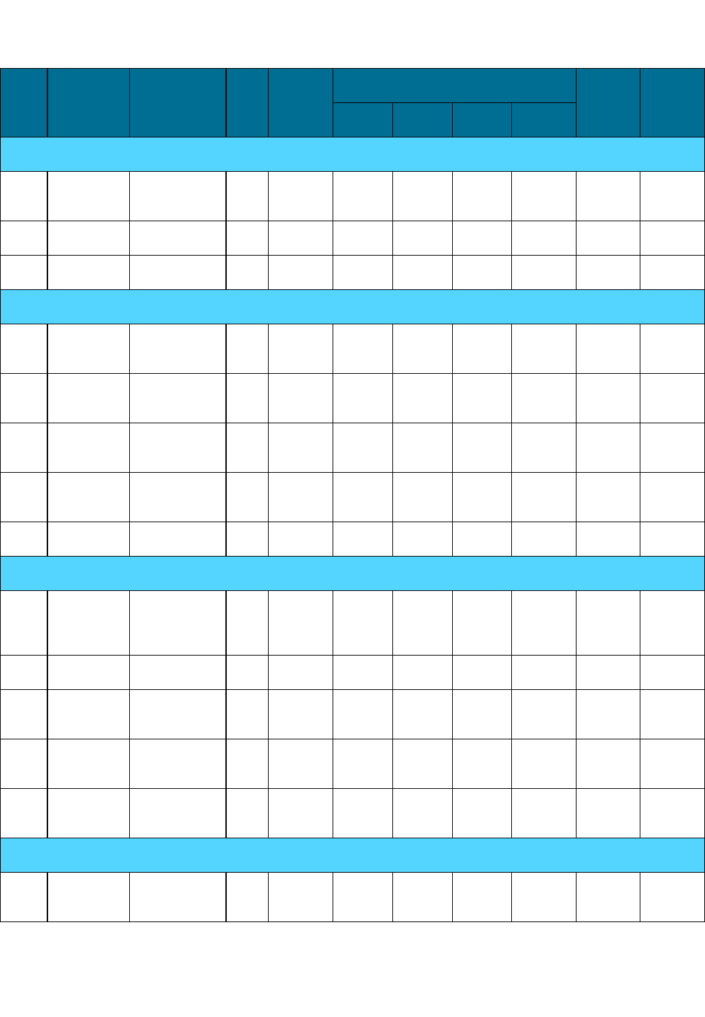
36 98-08901C66-G
USB:
10 USB_
VBUS USB- VCC I DC 5 V
12 USB_D+ USB_D+ 3.3 V
14 USB_D- USB_D- 3.3 V
SPI:
70 SPI_CS SPI chip-
select O Logic 2.775 V 69KΩ
PU H
62 SPI_IRQ
_N SPI interrupt I Logic 2.775 V 69KΩ
PD L
64 SPI_DIN SPI MISO
input I Logic 2.775 V 69KΩ
PU H
68 SPI_
DOUT
SPI MOSI
output O Logic 2.775 V H
66 SPI_CLK SPI clock O Logic 2.775 V H
SIM Card:
50 SIM_PD
_N
SIM-
presence
detect
I Logic 2.775 V 69KΩ
PU L
48 SIM_VCC SIM VCC O DC 1.8 3 V
44 SIM_RST
_N SIM reset O Logic 1.8 3 V 69KΩ
PD L
52 SIM_DIO SIM serial
data I/O Logic 1.8 3 V 22KΩ
PU H
46 SIM_CLK SIM clock O Logic 1.8 3 V 69KΩ
PD H
PCM Audio:
18 PCM_DIN Digital audio
receive I Logic 2.775 V 69KΩ
PD H
Table 13. g20 Interface Connector Pin Assignments (Continued)
Pin
#
Signal
Name Description I/O Signal
Level Inter-
nal
PU/PD
Active
H/L
Min Typ Max Units
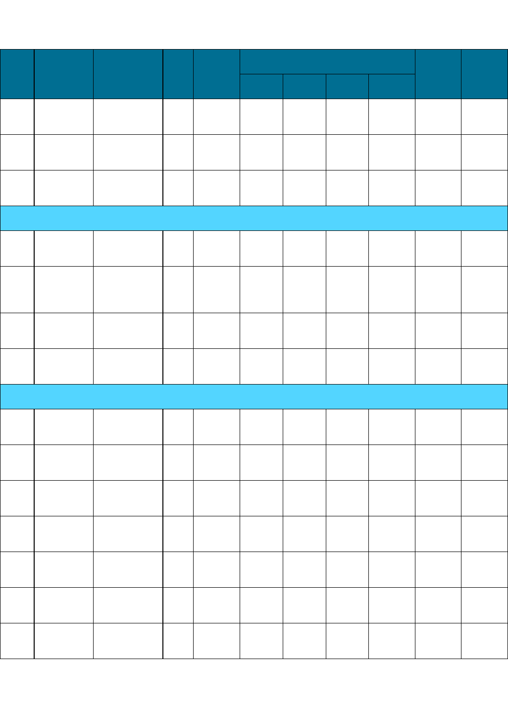
98-08901C66-G 37
20 PCM_
DOUT
Digital audio
transmit O Logic 2.775 V 69KΩ
PU H
22 PCM_
CLK
Digital audio
clock O Logic 2.775 V 69KΩ
PD H
24 PCM_FS Digital audio
frame sync O Logic 2.775 V 69KΩ
PD H
Display:
54 LCD_CS Display chip-
select O Logic 2.775 V H
60 LCD_RS
Display
register-
select
O Logic 2.775 V H
56 LCD_
DATA
Display
serial data O Logic 2.775 V H
58 LCD_CLK Display
serial clock O Logic 2.775 V H
Keypad:
30 KBC0_N Keypad
column 0 I Logic 2.775 V 22KΩ
PU L
28 KBC1_N Keypad
column 1 I Logic 2.775 V 22KΩ
PU L
32 KBR0_N Keypad
row 0 I Logic 2.775 V 22KΩ
PU L
34 KBR1_N Keypad
row 1 I Logic 2.775 V 22KΩ
PU L
36 KBR2_N Keypad
row 2 I Logic 2.775 V 22KΩ
PU L
38 KBR3_N Keypad
row 3 I Logic 2.775 V 22KΩ
PU L
40 KBR4_N Keypad
row 4 I Logic 2.775 V 22KΩ
PU L
Table 13. g20 Interface Connector Pin Assignments (Continued)
Pin
#
Signal
Name Description I/O Signal
Level Inter-
nal
PU/PD
Active
H/L
Min Typ Max Units
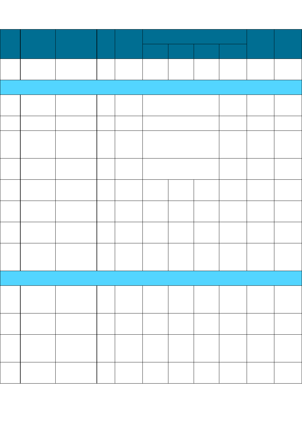
38 98-08901C66-G
42 KBR5_N Keypad
row 5 I Logic 2.775 V 22KΩ
PU L
Audio:
67 SPKR_N Speaker
inverted OAudio As described in section
3.4.1.2 V
69 SPKR_P Speaker O Audio Inverted SPKR_N V
63 ALRT_N
Alert
speaker
inverted
O Audio Inverted ALERT_P V
65 ALRT_P Alert
speaker OAudio As described in section
3.4.1.2 V
61 MIC Microphone
input IAudio
59 MIC_GND Microphone
ground GND
57 HDST_
MIC
Headset
microphone IAudio
55 HDST_
INT_N
Headset-
detect
interrupt
I Logic 2.775 V 270K
PU L
Charger:
35 CHRG_
DET_N
Charger-
presence
detect
I Logic 2.775 V L
33 CHRG_
STATE
Charger rate
indicator I Logic 2.775 V
31 CHRG_
SW
Accessory
current
control
O Logic 2.775 V
29 CHRG_
DIS
Charger
disable O Logic 2.775 V H
Table 13. g20 Interface Connector Pin Assignments (Continued)
Pin
#
Signal
Name Description I/O Signal
Level Inter-
nal
PU/PD
Active
H/L
Min Typ Max Units
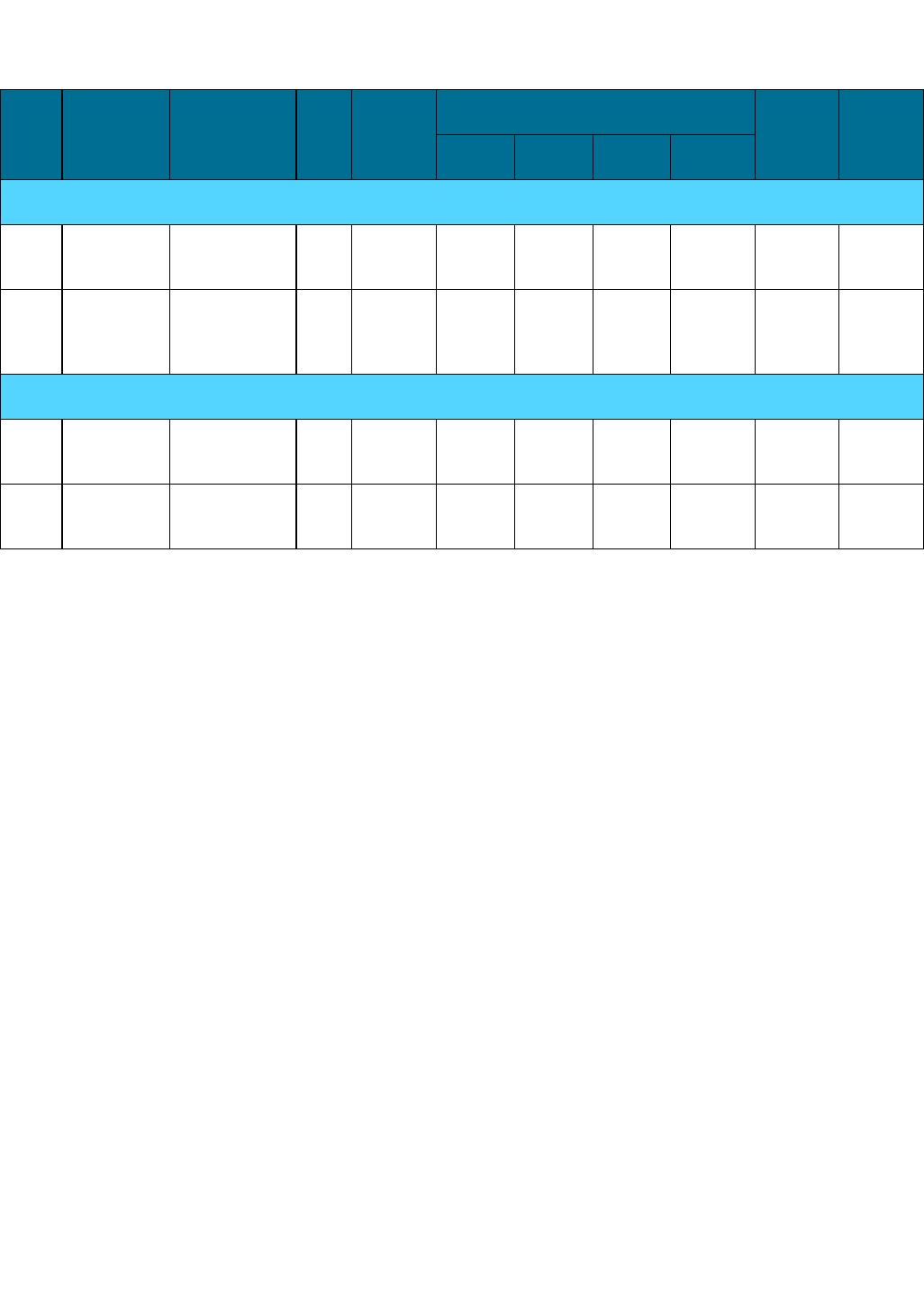
98-08901C66-G 39
ADC:
45 CHRG_
TYP
Accessory-
type detect I ADC 0 2.775 V 47KΩ
PU
47 THERM
Temperature
measure-
ment
I ADC 0 2.775 V
Miscellaneous:
27 BL_SINK Backlight
current sink IDC 80100mA
43 VIB_OUT Vibrator
regulator ODC 1.3 V
Table 13. g20 Interface Connector Pin Assignments (Continued)
Pin
#
Signal
Name Description I/O Signal
Level Inter-
nal
PU/PD
Active
H/L
Min Typ Max Units
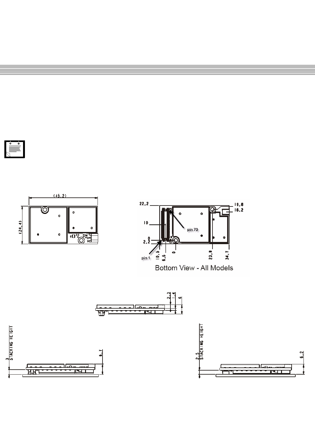
98-08901C66-G 41
5. MECHANICAL DESCRIPTION
5.1 MECHANICAL DETAILS
This section describes the mechanical details for the g20:
Size: 45.2x24.4x6 mm
Mounting: Two 2.4 mmØ holes are provided that accommodate M2 screws or #1-64 UNC 2A machine screws. Torque to
2.6 lb*inch (3kg*cm). Refer to Figure 17 below for mounting requirements.
Figure 17. Mechanical Mounting Requirements
Note
Motorola recommends using a split washer for vibrations.
Top View - All Models
Bottom View - All Models
Side View - All Models
Side View for F3003-F3004 Models Side View for F3012 & F3013 Models

98-08901C66-G 43
6. SERVICE SUPPORT
6.1 CUSTOMER ASSISTANCE
This section provides contact information for any possible queries that may arise, such as the following:
• Have questions?
• Having trouble getting the Developer Board set up?
• Technical questions?
• Configuration questions/problems?
• Technical operating problems?
• Need documentation?
The GSM/CDMA Data Module Customer Support Center is ready to assist you on integration issues.
A direct customer should use the following email address to contact customer assistance: n2cshd@motorola.com.
An indirect customer should send his requests to his distributor and not to Motorola help desk.
Every new call/problem report should be directed to the help desk email address noted above. It is recommended to report each
individual issue in a separate email. The following information is required when reporting a problem:
• Customer name and address
• Customer contact information for this request, including:
•Name
• Telephone
• Fax number
• Mobile number
• Email address
• Product name (for example, g20)
• Software version of the unit (ATI8 command) or model number
• PCB version: This information is located on the PCB near the RF connector.
• Severity of the problem
• Problem description, including:
• Operator name
• Type of SIM card (for example, Test, Pre-paid, or 5v/3v/1.8v)
• Configuration of the setup (such as Developer Board, handset, host, connections, and so on)
• Detailed scenario from startup
• Log of all the commands and the responses, beginning from startup
Note
The support services provided by Motorola are subject to the agreement between the customer and Motorola and
may be at an additional charge to the customer. Motorola will inform the customer in advance of any such charge.

44 98-08901C66-G
• Answers to the following questions:
• Was the same scenario tested on the Developer Board and the PC to reproduce the problem?
• How many units do you have, and how many of them have this problem?
• How often does the problem recur?
In addition to the information requested above, send the following AT commands and the HyperTerminal log with the
responses:
AT+CMEE=2 // To get textual error message
AT+CPIN? // To get SIM card status
AT+CREG? // To see if the TXVR is registered to the network
AT+CSQ // To get the signal strength (RX level)
AT+CGSN // To read the IMEI number of the unit
ATI3 // To get the software version of the TXVR
AT\S // To get the setting of basic AT commands
AT+CMER=0,0,1,1 // To get messages and indicators from the handset display to the DTE
6.1.1 Motorola Workflow
The help desk uses the following workflow when responding to new calls:
1. Each new call is registered in the help desk data base.
2. The help desk immediately notifies the customer with the help desk system record number for each issue.
3. A champion is assigned to be responsible for the new call, from arrival to closing.
4. During this time, the champion updates the help desk system with the progress of the resolution process.
5. The champion is the contact to the customer and the engineering team, and coordinates activities that are required to solve
the problem.
6.1.2 Service Centers
Motorola Electronics Taiwan PCS
11F, No, 296, Sec. 4, Jen-Ai Road
Taipei, 106, Taiwan, R.O.C
Motorola GmbH
Am Sophienhof 10
D-24941 Flensburg
Germany

98-08901C66-G 45
Motorola Communications ISRAEL Ltd.
Service Operation
Attention: Shukrun Ofer
3 Krementsky Street
Tel Aviv, Israel 67899
Telephone: (972) 3 5658829
JNB Electronics Pty Ltd.
347 Settlement Road, Thomastown
VIC 3074
Australia
Field service should be coordinated with the Service Manager in Motorola using the following email address:
N2CSFS01@motorola.com
6.1.3 Ordering Accessories
The following accessory items are available to aid the developer:
• Standard USB cable, A-type connector to B-type connector
• Standard RS232 cable, 9-pin male connected to the Developer Board
To place an order, contact your Motorola account manager. A list of Motorola account managers is available at
www.motorola.com/automotive/telematics/. Then, Click Products > Data Modules > Contact Us.
6.2 TESTING A STANDALONE UNIT
This section describes how to perform a functionality test on a g20 unit. The test is performed in order to:
• Introduce the user to the g20
• Explain how to work with the g20 unit
• Describe how to evaluate basic g20 features
The test setup provides a wide platform through which a g20 unit can be evaluated. The specific test procedure described below
covers only few of the g20’s many features. Using this setup, you can perform several additional tests on the g20.
The test is performed using two modems, one of which is the g20. The modems communicate with each other through a single
computer, which also controls their operation.
The test requires knowledge about the operation of the g20 Developer’s Kit, terminal applications and AT commands. Refer to
relevant documentation for assistance.
To perform the test, you need the following:
• A g20 OEM cellular engine unit
• A g20 Developer's Kit
• A desktop or laptop computer, which includes:
•· A free serial communications port (RS232)
•· A connected and active line modem (internal or external)
•· A terminal application (such as HyperTerminal)
46 98-08901C66-G
6.2.1 Test Setup
Follow the procedure below to set up your equipment before performing the test:
1. Verify that the computer you intend to use for the test is equipped with a working line modem.*
2. Set up the g20 and the Developer Board as described in the Initial Setup section of the g20 Developer’s Kit document by
doing the following:
• Verify that the g20 has adequate reception from the local GSM network.
• Connect the Developer Board’s RS232 port to the computer’s serial port.
3. Open a terminal application window (such as HyperTerminal) in the computer and configure it to operate with the serial
port occupied by the g20.
4. Open a second terminal window and configure it to operate with the serial port occupied by the line modem.
Figure 18. Test Setup
*You can use a second g20 unit instead of the line modem. When doing so, you must repeat the setup procedure for the additional g20.
6.2.2 Test Procedure
Follow the procedure below to perform the g20 test:
1. Verify that the g20 is functioning and communicating with the computer by performing the following AT commands in
the g20 terminal window:
•ati7: This prompts g20 identification. The g20 will reply "G20 OEM Module".
•ati8: This command prompts the g20 software version.
2. Verify that the line modem is functioning and communicating with the computer by entering the AT command "at" in the
modem’s terminal window. This common AT command prompts a properly working modem to reply "OK".
3. Make a CSD data call from the g20 to the line modem or vice versa using the "atdt" and "ata" commands in the appropriate
window.
4. Verify that a connection between the two modems is established.
5. Select any file to be transferred between the two modems. The file can be any existing file on the computer, or a new file
created specifically for the test.
6. Send the file through the terminal application, from the g20 or to it, using the terminal application’s send/receive file
options.
7. When the file transfer is completed, use the "ath" command in any of the terminal windows to terminate the call. This step
completes the test. You can now continue to perform additional tests using the same setup, or change the setup as required.
Computer Developer Board
with g20 unit
Line Modem
(internal or external)
To telephone line
wall outlet RS232
Port
Serial
Port
Serial
Port
Serial
Cable

98-08901C66-G 47
7. INDEX
A
Abbreviations 7
Analog
Input 26
Output 26
Analog Audio Connectivity 15
Antenna Installation 12
Approvals
Regulatory 11
Audio Interfaces 26
Analog 26
B
Block Diagram Description 13
C
Communication Interfaces 21
RS232 22
Connections
Additional 16
SIM v, 24
SPI 25
USB 23
Connectivity
Analog Audio 15
DCE 20
Digital Audio 15
DTE 20
RS232 15
Connectors 33
Current Consumption 17
D
DCE Connectivity 20
DTE Connectivity 20
E
Environmental
Specifications 9
G
g20
Abbreviations 7
Analog Audio Interfaces 26
Analog Input 26
Analog Output 26
Antenna Detect 26
Antenna Installation 12
Audio Interfaces 26
Block Diagram 13
Block Diagram Description 13
Communication Interfaces 21
Connections 16
Connectivity 15
Connectors 33
Current Consumption 17
DCE/DTE Connectivity 20
GPRS Coverage Indication 25
Ignition Line 19
Interfaces 25
Models Description 11
On/Off Signal 19
Operation Overview 13
Pin Assignments 34
Power Supply 17
Product Specifications 9
Regulatory Approvals 11
RS232 15, 22
RS232 Connection 22
RS232 Levels 22
Safety Precautions 12
SIM 24
SIM Connection v, 24
Sleep Mode Options 19
SPI 25
SPI Connection 25
Standards 1

48 98-08901C66-G
Terms and Abbreviations 7
Testing 45
Trademarks 2
Transmit Enable 25
Turning the Unit On/Off 18
USB 23
USB Connection 23
User Operation 12
I
Ignition Line 19
Interfaces 25
Analog Audio 26
Audio 26
M
Models Description 11
O
Off
Turn the Unit 18
On
Turn the Unit 18
Operation Overview 13
P
Physical Specifications 9
Pin
Antenna Detect 26
GPRS Coverage Indication 25
Transmit Enable 25
Pin Assignments 34
Power Supply 17
Design 17
RF Filtering v, 17
Precautions 12
Product Specifications 9
R
Regulatory Approvals 11
RS232 15, 22
Analog Audio Connectivity 15
Connection 22
Digital Audio Connectivity 15
Levels 22
S
Safety Precautions 12
Signal
On/Off 19
SIM 24
Sleep Mode Options 19
General 19
Specifications 9
Environmental 9
Physical 9
SPI 25
Standards 1
T
Terms 7
Testing 45
Test Procedure 46
Test Setup 46
Trademarks 2
Turning the Unit On/Off 18
U
USB 23
User Operation 12

*98-08901C66-G*
98-08901C66-G
MOTOROLA and the Stylized M Logo are registered in the US Patent & Trademark Office.
All other product or service names are the property of their respective owners.
©Copyright 2004 Motorola, Inc.
Java™ Technology and/or J2ME™ : Java and all other Java–based marks are trademarks or registered
trademarks of Sun Microsystems, Inc. in the U.S. and other countries.
UNIX® : UNIX is a registered trademark of The Open Group in the United States and other countries.