Motorola Mobility T56DB2 Dual Band GSM Development Module User Manual g20 Developer s Kit
Motorola Mobility LLC Dual Band GSM Development Module g20 Developer s Kit
Contents
- 1. Exhibit 8 Users Manual
- 2. Exhibit 8 a1 Users Manual per CRN22341
- 3. Exhibit 8 b1 Users Manual per CRN22341
Exhibit 8 b1 Users Manual per CRN22341
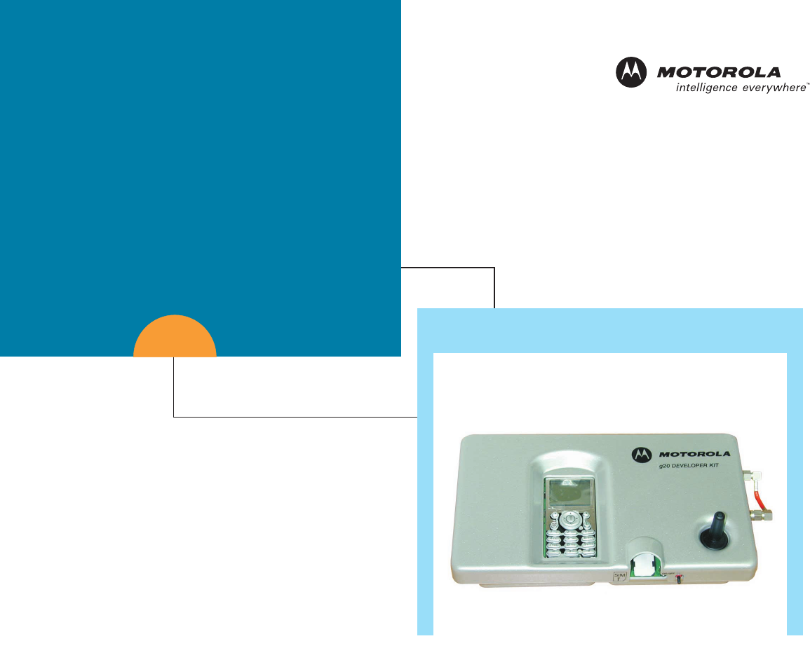
Developer's Guide
Motorola g20
Developer’s Kit
98-08901C67-D
SPECIFICATIONS SUBJECT TO CHANGE WITHOUT NOTICE
Notice
While reasonable efforts have been made to assure the accuracy of this document, Motorola, Inc. assumes no liability resulting
from any inaccuracies or omissions in this document, or from use of the information obtained herein. The information in this
document has been carefully checked and is believed to be entirely reliable. However, no responsibility is assumed for
inaccuracies or omissions. Motorola, Inc. reserves the right to make changes to any products described herein and reserves the
right to revise this document and to make changes from time to time in content hereof with no obligation to notify any person of
revisions or changes. Motorola, Inc. does not assume any liability arising out of the application or use of any product, software, or
circuit described herein; neither does it convey license under its patent rights or the rights of others.
It is possible that this publication may contain references to, or information about Motorola products (machines and programs),
programming, or services that are not announced in your country. Such references or information must not be construed to mean
that Motorola intends to announce such Motorola products, programming, or services in your country.
Copyrights
This instruction manual, and the Motorola products described in this instruction manual may be, include or describe copyrighted
Motorola material, such as computer programs stored in semiconductor memories or other media. Laws in the United States and
other countries preserve for Motorola and its licensors certain exclusive rights for copyrighted material, including the exclusive
right to copy, reproduce in any form, distribute and make derivative works of the copyrighted material. Accordingly, any
copyrighted material of Motorola and its licensors contained herein or in the Motorola products described in this instruction
manual may not be copied, reproduced, distributed, merged or modified in any manner without the express written permission of
Motorola. Furthermore, the purchase of Motorola products shall not be deemed to grant either directly or by implication, estoppel,
or otherwise, any license under the copyrights, patents or patent applications of Motorola, as arises by operation of law in the sale
of a product.
Computer Software Copyrights
The Motorola and 3rd Party supplied Software (SW) products described in this instruction manual may include copyrighted
Motorola and other 3rd Party supplied computer programs stored in semiconductor memories or other media. Laws in the United
States and other countries preserve for Motorola and other 3rd Party supplied SW certain exclusive rights for copyrighted
computer programs, including the exclusive right to copy or reproduce in any form the copyrighted computer program.
Accordingly, any copyrighted Motorola or other 3rd Party supplied SW computer programs contained in the Motorola products
described in this instruction manual may not be copied (reverse engineered) or reproduced in any manner without the express
written permission of Motorola or the 3rd Party SW supplier. Furthermore, the purchase of Motorola products shall not be deemed
to grant either directly or by implication, estoppel, or otherwise, any license under the copyrights, patents or patent applications of
Motorola or other 3rd Party supplied SW, except for the normal non-exclusive, royalty free license to use that arises by operation
of law in the sale of a product.
VENDOR COPYRIGHT
Apache Software Foundation Copyright 2002-2003 All Rights Reserved
Artesyn Copyright 2002-2003 All Rights Reserved
CMU * Copyright 2002-2003 All Rights Reserved
Freeware Tools / Utilities * Copyright 2002-2003 All Rights Reserved
Performance Technologies Copyright 2002-2003 All Rights Reserved
Telelogic Copyright 2002-2003 All Rights Reserved
QNX * Copyright 2002-2003 All Rights Reserved
*= Freeware

Usage and Disclosure Restrictions
License Agreements
The software described in this document is the property of Motorola, Inc. and its licensors. It is furnished by express license
agreement only and may be used only in accordance with the terms of such an agreement.
Copyrighted Materials
Software and documentation are copyrighted materials. Making unauthorized copies is prohibited by law. No part of the software
or documentation may be reproduced, transmitted, transcribed, stored in a retrieval system, or translated into any language or
computer language, in any form or by any means, without prior written permission of Motorola, Inc.
High Risk Materials
Components, units, or third-party products used in the product described herein are NOT fault-tolerant and are NOT designed,
manufactured, or intended for use as on-line control equipment in the following hazardous environments requiring fail-safe
controls: the operation of Nuclear Facilities, Aircraft Navigation or Aircraft Communication Systems, Air Traffic Control, Life
Support, or Weapons Systems (High Risk Activities"). Motorola and its supplier(s) specifically disclaim any expressed or implied
warranty of fitness for such High Risk Activities.
Trademarks
MOTOROLA and the Stylized M Logo are registered in the US Patent & Trademark Office. All other product or service names are
the property of their respective owners.
©Copyright 2005 Motorola, Inc.
Java™ Technology and/or J2ME™: Java and all other Java-based marks are trademarks or registered trademarks of Sun
Microsystems, Inc. in the U.S. and other countries.
UNIX®: UNIX is a registered trademark of The Open Group in the United States and other countries.
REV052604
Developer’s Guide
98-08901C67-D
© Motorola Communications Ltd., 2005
A subsidiary of Motorola Inc.
All rights reserved.
g20 Developer’s Kit

v 98-08901C67-D
REVISION HISTORY
Revision Date Purpose
O 30 June 2003 Initial release
A 15 February 2004 Removed 2 g20 models
Changes in para. 3.4.2.2 regarding USB driver
B 1 March 2004 Updated Table 22 - g20 Connectors Pinout
C 4 July 2004 Updated section 2.2, Package Contents
Updated section 3.4.5.1, Wakeup
Updated section 3.5.2, Switches and Jumpers
Updated section 3.5.3, LED Indicators
Updated section 5.1, Developer Board Parts List
D April 2005 New sections: “LIMITATION OF LIABILITY” on page 3 and “WARRANTY
NOTIFICATION” on page 4
Updated section 3.5.4, MMI

July 2004
© Motorola Inc., 2004 98-08901C67-D
g20 Developer’s Kit
CONTENTS
REVISION HISTORY ................................................................................................................................................................v
PREFACE
1.1 SCOPE OF THIS MANUAL .................................................................................................................................................1
1.2 WHO SHOULD USE THIS MANUAL.................................................................................................................................1
1.3 DISCLAIMER........................................................................................................................................................................1
1.4 SAFETY .................................................................................................................................................................................1
1.4.1 Precautions ..................................................................................................................................................................1
1.4.2 User Operation ............................................................................................................................................................2
1.4.3 Antenna Installation ....................................................................................................................................................2
1.5 APPLICABLE DOCUMENTS ..............................................................................................................................................2
1.6 TRADEMARKS.....................................................................................................................................................................2
1.7 TERMS AND ABBREVIATIONS ........................................................................................................................................3
1.8 HOW THIS MANUAL IS ORGANIZED..............................................................................................................................3
1.9 LIMITATION OF LIABILITY..............................................................................................................................................3
1.10 WARRANTY NOTIFICATION ..........................................................................................................................................4
1.10.1 HOW TO GET WARRANTY SERVICE?...............................................................................................................4
1.10.2 CLAIMING...............................................................................................................................................................5
1.10.3 CONDITIONS ..........................................................................................................................................................5
1.10.4 WHAT IS NOT COVERED BY THE WARRANTY..............................................................................................5
1.10.5 INSTALLED DATA.................................................................................................................................................6
1.10.6 OUT OF WARRANTY REPAIRS...........................................................................................................................6
INTRODUCTION
2.1 GENERAL DESCRIPTION...................................................................................................................................................7
2.2 PACKAGE CONTENTS........................................................................................................................................................9
2.3 ACCESSORIES....................................................................................................................................................................10
DEVELOPER BOARD AND INTERFACES DESCRIPTION
3.1 HOW THIS CHAPTER IS ORGANIZED...........................................................................................................................11
3.2 OVERVIEW .........................................................................................................................................................................11
3.2.1 Developer Board Features.........................................................................................................................................11

vii 98-08901C67-D
3.2.2 Developer Board Components.................................................................................................................................. 12
3.3 INITIAL SETUP.................................................................................................................................................................. 13
3.3.1 g20 ............................................................................................................................................................................ 13
3.3.2 External Connectors ................................................................................................................................................. 14
3.4 CONFIGURATION............................................................................................................................................................. 16
3.4.1 Alternate Power Sources .......................................................................................................................................... 16
3.4.2 Communication Interfaces........................................................................................................................................ 19
3.4.3 Audio Interface......................................................................................................................................................... 22
3.4.4 Antenna..................................................................................................................................................................... 25
3.4.5 Option Switches........................................................................................................................................................ 26
3.4.6 SIM Card .................................................................................................................................................................. 27
3.4.7 Host Connection ....................................................................................................................................................... 28
3.5 COMPONENTS AND SPECIFICATIONS ........................................................................................................................ 29
3.5.1 Connectors Description ............................................................................................................................................ 29
3.5.2 Switches and Jumpers............................................................................................................................................... 32
3.5.3 LED Indicators ......................................................................................................................................................... 34
3.5.4 MMI.......................................................................................................................................................................... 36
3.5.5 AC Adapter Detection Circuit .................................................................................................................................. 36
3.5.6 Electrical Specifications ........................................................................................................................................... 36
SERVICE SUPPORT
4.1 CUSTOMER ASSISTANCE............................................................................................................................................... 37
4.1.1 Motorola Workflow.................................................................................................................................................. 38
4.1.2 Service Centers......................................................................................................................................................... 38
4.2 TROUBLESHOOTING....................................................................................................................................................... 40
PARTS LIST
5.1 DEVELOPER BOARD PARTS LIST................................................................................................................................. 43
5.2 DEVELOPER BOARD UNPLACED PARTS LIST .......................................................................................................... 49
INDEX
SCHEMATICS AND
PLACEMENT DIAGRAMS

98-08901C67-D viii
LIST OF FIGURES
Figure 1. g20 Developer’s Kit (top view, with cover) ................................................................................................................. 7
Figure 2. g20 Developer’s Kit (front, with cover) ....................................................................................................................... 8
Figure 3. g20 Developer’s Kit (left side, with cover) .................................................................................................................. 8
Figure 4. g20 Developer’s Kit (rear, with cover)......................................................................................................................... 8
Figure 5. g20 Developer’s Kit (right side, with cover) ................................................................................................................ 8
Figure 6. g20 Developer’s Kit with Accessories and the g20.................................................................................................... 10
Figure 7. Developer Board Components.................................................................................................................................... 12
Figure 8. Connecting the g20..................................................................................................................................................... 13
Figure 9. Developer Board Power Switch and Adapter Connector ........................................................................................... 14
Figure 10. Audio Connectors ..................................................................................................................................................... 15
Figure 11. SIM Tray................................................................................................................................................................... 15
Figure 12. Power Supply Connectors, Jumpers and Switches ................................................................................................... 16
Figure 13. DC Power Connectors .............................................................................................................................................. 17
Figure 14. USB, RS232 and Diagnostics Connectors................................................................................................................ 19
Figure 15. Audio Connectors and Jumper.................................................................................................................................. 22
Figure 16. Antenna Connectors (external) ................................................................................................................................. 25
Figure 17. Antenna Connectors (internal).................................................................................................................................. 25
Figure 18. Option Switches........................................................................................................................................................ 26
Figure 19. 70-pin Connectors..................................................................................................................................................... 28
Figure 20. Jumpers and Switches on Developer Board ............................................................................................................. 32
Figure 21. LEDs on Developer Board........................................................................................................................................ 34

98-08901C67-D x
LIST OF TABLES
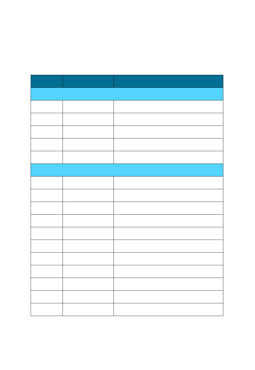
Table 1. Terms and Abbreviations ............................................................................................................................................... 3
Table 2. g20 Developer’s Kit Package Contents.......................................................................................................................... 9
Table 3. Accessories Sold Separately ........................................................................................................................................ 10
Table 4. Power Adapter Connector Pinout (J230) ..................................................................................................................... 17
Table 5. Battery Connector Pinout (P600)................................................................................................................................. 18
Table 6. Power Source Jumper (P202)....................................................................................................................................... 18
Table 7. Developer Board Power Jumper (P201) ...................................................................................................................... 18
Table 8. g20 Power Jumper (P201)............................................................................................................................................ 19
Table 9. RS232-1 Connector Pinout (J350) ............................................................................................................................... 20
Table 10. USB Connector Pinout (J300).................................................................................................................................... 20
Table 11. USB Jumper (P300) ................................................................................................................................................... 21
Table 12. Diagnostics Connector Pinout (J500)......................................................................................................................... 21
Table 13. Speaker Connector Pinout (J430)............................................................................................................................... 22
Table 14. Microphone Connector Pinout (J460)........................................................................................................................ 23
Table 15. Audio Jumper (P420) ................................................................................................................................................. 23
Table 16. Headset Connector Pinout (J440)............................................................................................................................... 24
Table 17. Alert Transducer Pinout (LS400)............................................................................................................................... 24
Table 18. Option Switches ......................................................................................................................................................... 26
Table 19. SIM Connector Pinout (J100) .................................................................................................................................... 27
Table 20. SIM Card Detect Logic Jumper (P110) ..................................................................................................................... 27
Table 21. Connectors.................................................................................................................................................................. 29
Table 22. g20 Connectors Pinout ............................................................................................................................................... 30
Table 23. Switches and Jumpers ................................................................................................................................................ 32
Table 24. LEDs .......................................................................................................................................................................... 34
Table 25. Electrical Specifications............................................................................................................................................. 36
Table 26. Troubleshooting ......................................................................................................................................................... 40
Table 27. Developer Board Parts List ........................................................................................................................................ 43
Table 28. Developer Board Unplaced Parts List........................................................................................................................ 49

98-08901C67-D 1
1. PREFACE
1.1 SCOPE OF THIS MANUAL
This manual introduces the g20 Developer's Kit, and describes the technical details required by the user to successfully integrate
the Motorola g20 cellular engine into an original equipment manufacturer (OEM) wireless host device. With the help of this
manual, the user can utilize the Developer's Kit to conduct a full series of test and evaluation procedures on the g20, as well as
perform application development.
We at Motorola want to make this guide as helpful as possible. Keep us informed of your comments and suggestions for
improvements.
You can reach us by email: n2cshd@motorola.com.
1.2 WHO SHOULD USE THIS MANUAL
This manual is intended for all members of the integration team who are responsible for integrating the g20 into the host appli-
cation, including representatives from hardware, software and RF engineering disciplines.
1.3 DISCLAIMER
This guide provides advice and guidelines to developers. Responsibility regarding how the information is used lies entirely with
the user. Statements indicating support provided by, or offered by, Motorola are subject to change at any time.
Motorola reserves the right to make any changes to this manual.
1.4 SAFETY
1.4.1 Precautions
Most Developer Board circuits are not shielded. Be sure to take appropriate precautionary measures in order to avoid ESD while
handling the kit. ESD can damage the Developer Board and/or the g20 module attached to it.

2 98-08901C67-D
1.4.2 User Operation
Do not operate your unit when a person is within eight inches (20 centimeters) of the antenna. A person or object within eight
inches (20 centimeters) of the antenna could impair call quality and may cause the unit to operate at a higher power level than
necessary, as well as expose that person to RF energy in excess of that established by the FCC RF Exposure Guidelines.
IMPORTANT: The unit must be installed in a manner that provides a minimum separation distance of eight inches (20 centi-
meters) or more between the antenna and persons in order to satisfy FCC RF exposure requirements for mobile transmitting
devices.
IMPORTANT: To comply with the FCC RF exposure limits and to satisfy the categorical exclusion requirements for mobile
transmitters, the requirements described in the following section must be met.
1.4.3 Antenna Installation
• A minimum separation distance of eight inches (20 centimeters) must be maintained between the antenna and all persons.
• The effective radiated power of the transmitter must be less than 3.0 Watts ERP (4.9 Watts or 36.9 dBm EIRP). This requires
that the combination of antenna gain and feed line loss should not exceed 9.9 dBi.
1.5 APPLICABLE DOCUMENTS
• g20 Cellular Engine Module Description: 9808901C66-G
• g20 AT Commands: 9808901C68-F
1.6 TRADEMARKS
MOTOROLA and the Stylized M Logo are registered in the U.S. Patent and Trademark Office. All other product and service
names are the property of their respective owners.
© Motorola, Inc. 2005
98-08901C67-D 3
1.7 TERMS AND ABBREVIATIONS
This section provides definitions for terms and abbreviations used in this document.
1.8 HOW THIS MANUAL IS ORGANIZED
This manual contains the following chapters:
•Chapter 1 contains this preface.
•Chapter 2 introduces the g20 Developer’s Kit.
•Chapter 3 describes the Developer Board and its components in detail, including connectors, jumpers, Dip switches and
LED indicators. It also includes a set of setup procedures for first-time use.
•Chapter 4 provides contact information for Motorola Service Support and Customer Assistance.
•Chapter 5 provides a parts list for the g20 Developer’s Kit.
1.9 LIMITATION OF LIABILITY
The Products are not designed, intended, or authorized for use as components in systems intended for surgical implant into the
body; in other applications intended to support or sustain life; for the planning, construction, maintenance, operation or use of
any nuclear facility; for the flight, navigation, communication of aircraft or ground support equipment; or in any other applica-
tion in which the failure of the Product could create a situation where personal injury or death may occur. If CUSTOMER should
Table 1. Terms and Abbreviations
Acronym/Term Definition/Description
ADC Analog to Digital Converter
CMOS Complementary Metal Oxide Semiconductor
CODEC Coder-Decoder
DIAG Diagnostics
DTE Data Terminal Equipment (such as terminals, PCs and so on)
EME Electromagnetic Emission
ESD Electro-Static Discharge
EVB Evaluation Board
GPRS General Packet Radio Service
GSM Global System for Mobile Communications
IRQ Interrupt Request
LED Light-Emitting Diode
MIDI Musical Instrument Digital Interface
MMCX Mini Micro Coax
MMI Man-Machine Interface
OEM Original Equipment Manufacturer
PCM Pulse Code Modulation
RF Radio Frequency
SIM Subscriber Identity Module
SPI Serial Peripheral Interface
UART Universal Asynchronous Receiver Transmitter
USB Universal Serial Bus
UUT Unit Under Test

4 98-08901C67-D
use any Product or provide any Product to a third party for any such use, CUSTOMER hereby agrees that MOTOROLA is not
liable, in whole or in part, for any claims or damages arising from such use, and further agrees to indemnify and hold MOTOR-
OLA harmless from any claim, loss, cost or damage arising from such use.
EXCEPT AS SPECIFICALLY STATED ABOVE, THE PRODUCTS ARE PROVIDED "AS IS" AND MOTOROLA
MAKES NO OTHER WARRANTIES EXPRESS, IMPLIED, STATUTORY, OR OTHERWISE REGARDING THE PROD-
UCTS. MOTOROLA SPECIFICALLY DISCLAIMS ANY IMPLIED WARRANTIES OF MERCHANTABILITY AND
FITNESS FOR A PARTICULAR PURPOSE, OR ARISING FROM A COURSE OF DEALING OR USAGE OF TRADE.
Under no circumstances shall MOTOROLA be liable to CUSTOMER or any other party for any costs, lost revenue or profits
or for any other special, incidental or consequential damages, even if MOTOROLA has been informed of such potential loss or
damage. And in no event shall MOTOROLA's liability to CUSTOMER for damages of any nature exceed the total purchase
price CUSTOMER paid for the Product at issue in the dispute, except direct damages resulting from patent and/or copyright
infringement, which shall be governed by the "INDEMNITY" Section of this Agreement.
The preceding states MOTOROLA's entire liability for MOTOROLA's breach or failure to perform under any provision of this
Agreement.
1.10 WARRANTY NOTIFICATION
Motorola guarantees to you, the original purchaser, the Personal Communicator and accessories which you have purchased from
an authorised Motorola dealer (the "Products"), to be in conformance with the applicable Motorola specifications current at the
time of manufacture for a term of [1] year from date of purchase of the Product(s) (Warranty Term).
You must inform Motorola of the lack of conformity to the applicable specifications of any of the Products within a period of
two (2) months from the date on which you detect a defect in material, workmanship or lack of conformity and in any event
within a term not to exceed the Warranty Term, and must immediately submit the Product for service to Motorola's Authorised
Repair or Service Center. Motorola shall not be bound by Product related statements not directly made by Motorola nor any
warranty obligations applicable to the seller.
A list of the Motorola Call Center numbers is enclosed with this Product.
During the Warranty term, Motorola will, at its discretion and without extra charge, as your exclusive remedy, repair or replace
your Product which does not comply with this warranty; or failing this, to reimburse the price of the Product but reduced to take
into account the use you have had of the Product since it was delivered. This warranty will expire at the end of the Warranty
Term.
This is the complete and exclusive warranty for a Motorola Personal Communicator and accessories and in lieu of all other
warranties, terms and conditions, whether express or implied.
Where you purchase the product other than as a consumer, Motorola disclaims all other warranties, terms and conditions express
or implied, such as fitness for purpose and satisfactory quality.
In no event shall Motorola be liable for damages nor loss of data in excess of the purchase price nor for any incidental special
or consequential damages* arising out of the use or inability to use the Product, to the full extent such may be disclaimed by law.
This Warranty does not affect any statutory rights that you may have if you are a consumer, such as a warranty of satisfactory
quality and fit for the purpose for which products of the same type are normally used under normal use and service, nor any
rights against the seller of the Products arising from your purchase and sales contract.
(*)including without limitation loss of use, loss of time, loss of data, inconvenience, commercial loss, lost profits or savings.
1.10.1 HOW TO GET WARRANTY SERVICE?
In most cases the authorised Motorola dealer which sold and/or installed your Motorola Personal Communicator and original
accessories will honour a warranty claim and/or provide warranty service. Alternatively, for further information on how to get
warranty service please contact either the customer service department of your service provider or Motorola's call Center at the
telephone numbers below for your country.

98-08901C67-D 5
1.10.2 CLAIMING
In order to claim the warranty service you must return the Personal Communicator and/or accessories in question to Motorola's
Authorised Repair or Service Center in the original configuration and packaging as supplied by Motorola .Please avoid leaving
any supplementary items like SIM cards. The Product should also be accompanied by a label with your name, address, and
telephone number; name of operator and a description of the problem. In the case of vehicular installation, the vehicle in which
the Personal Communicator is installed should be driven to the Authorised Repair or Service Center, as analysis of any problem
may require inspection of the entire vehicular installation.
In order to be eligible to receive warranty service, you must present your receipt of purchase or a comparable substitute proof
of purchase bearing the date of purchase. The phone should also clearly display the original compatible electronic serial number
(IMEI) and mechanic serial number [MSN]. Such information is contained with the Product.
You must ensure that all and any repairs or servicing is handled at all times by a Motorola Authorised Service Center in accor-
dance with the Motorola Service requirements
In some cases, you may be requested to provide additional information concerning the maintenance of the Products by Motorola
Authorised Service Centers only, therefore it is important to keep a record of any previous repairs, and make them available if
questions arise concerning maintenance
1.10.3 CONDITIONS
This warranty will not apply if the type or serial numbers on the Product has been altered, deleted, duplicated, removed, or made
illegible. Motorola reserves the right to refuse free-of-charge warranty service if the requested documentation can not be
presented or if the information is incomplete, illegible or incompatible with the factory records.
Repair, at Motorola's option, may include reflashing of software, the replacement of parts or boards with functionally equivalent,
reconditioned or new parts or boards. Replaced parts, accessories, batteries, or boards are warranted for the balance of the orig-
inal warranty time period. The Warranty Term will not be extended. All original accessories, batteries, parts, and Personal
Communicator equipment that have been replaced shall become the property of Motorola. Motorola does not warrant the instal-
lation, maintenance or service of the products, accessories, batteries or parts.
Motorola will not be responsible in any way for problems or damage caused by any ancillary equipment not furnished by Motor-
ola which is attached to or used in connection with the Products, or for operation of Motorola equipment with any ancillary
equipment and all such equipment is expressly excluded from this warranty.
When the Product is used in conjunction with ancillary or peripheral equipment not supplied by Motorola, Motorola does not
warrant the operation of the Product/peripheral combination and Motorola will not honour any warranty claim where the Prod-
uct is used in such a combination and it is determined by Motorola that there is no fault with the Product. Motorola specifically
disclaims any responsibility for any damage, whether or not to Motorola equipment, caused in any way by the use of the Personal
Communicator, accessories, software applications and peripherals (specific examples include, but are not limited to: batteries,
chargers, adapters, and power supplies) when such accessories ,software applications and peripherals are not manufactured and
supplied by Motorola.
1.10.4 WHAT IS NOT COVERED BY THE WARRANTY
This warranty is not valid if the defects are due to damage, misuse, tampering, neglect or lack of care and in case of alterations
or repair carried out by unauthorised persons.
The following are examples of defects or damage not covered by this product warranty
1. Defects or damage resulting from use of the Product in other than its normal and customary manner.
2. Defects or damage from misuse, access to incompatible sources, accident or neglect.
3. Defects or damage from improper testing, operation, maintenance, installation, adjustment, unauthorised software appli-
cations or any alteration or modification of any kind.

6 98-08901C67-D
4. Breakage or damage to antennas unless caused directly by defects in material or workmanship.
5. Products disassembled or repaired other than by Motorola in such a manner as to adversely affect performance or prevent
adequate inspection and testing to verify any warranty claim.
6. Defects or damage due to range, coverage, availability, grade of service, or operation of the cellular system by the cellular
operator.
7. Defects or damage due to moist, liquid or spills of food.
8. Control unit coil cords in the Product that are stretched or have the modular tab broken.
9. All plastic surfaces and all other externally exposed parts that are scratched or damaged due to customer normal use.
10. Leather cases (which are covered under separate manufacturer's warranties).
11. Products rented on a temporary basis.
12. Periodic maintenance and repair or replacement of parts due to normal wear and tear.
The warranty for Motorola rechargeable batteries becomes void if (i) the batteries are charged other than by Motorola approved
battery chargers specified for the charging of the battery, (ii) any of the seals on the battery are broken or show evidence of
tampering, (iii) the battery is used in equipment or service other than the cellular telephone equipment for which it is specified.
Depending on operating conditions and your usage habits, wear and tear might take place of components including mechanical
problems related to Product housing, paint, assembly, sub-assemblies, displays and keyboards and any accessories which are
not part of the Product's in-box configuration. The rectification of faults generated through wear and tear and the use of consum-
able items like batteries beyond their Optimum Performance Time as indicated in the product manual is considered to be your
responsibility and therefore Motorola will not provide the free Warranty repair service for these items
1.10.5 INSTALLED DATA
Please make and retain a note of all data you have inserted into your Product for example names, addresses, phone numbers,
user and access codes, notes etc before submitting your Product for a Warranty service as such data may be deleted or erased as
part of the repair or service process.
Please note if you have downloaded material onto your Product, for example ring tones, ring tunes, screensavers, wallpaper,
games etc these may be deleted or erased as part of the repair process or testing process. Motorola shall not be responsible for
such matters. The repair or testing process should not affect any such material that was installed by Motorola on your Product
as a standard feature.
1.10.6 OUT OF WARRANTY REPAIRS
If you request Motorola to repair your Product any time after the Warranty term or where this warranty does not apply due to
the nature of the defect or fault, then Motorola may in its discretion carry out such repairs subject to you paying Motorola its
fees for such a repair or it may refer you to an authorised third party to carry out such repairs.
Note
The talk-time, stand-by time and total life cycle of a Motorola rechargeable battery for your Personal
Communicator will depend on usage conditions and network configurations. As a consumable product, the
specifications indicate that you should be able to obtain optimum performance for your Motorola Personal
Communicator within the first six months from date of purchase and up-to (200) charges(Optimum Perfor-
mance Time).
98-08901C67-D 7
2. INTRODUCTION
2.1 GENERAL DESCRIPTION
The g20 Developer’s Kit is intended for evaluating the g20 module, as well as for developing and testing software applications
for it.
The main component of the g20 Developer’s Kit is the Developer Board, which is mounted in a chassis. The kit includes a cover
for the Developer Board. The cover has openings on the top and sides for the Developer Board’s external connectors.
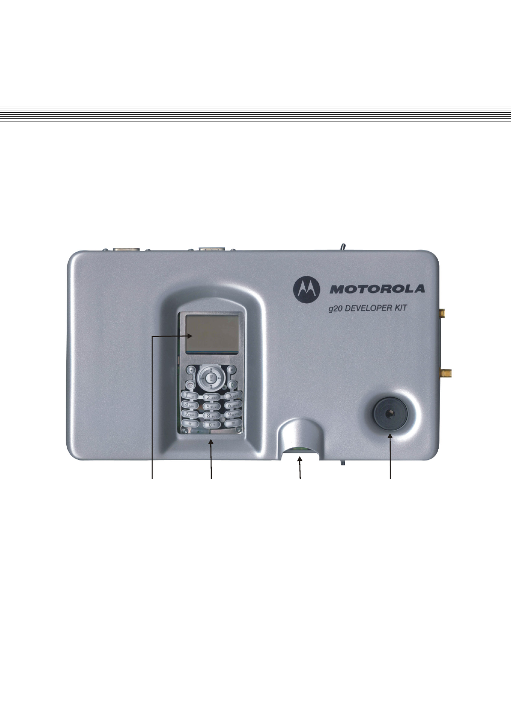
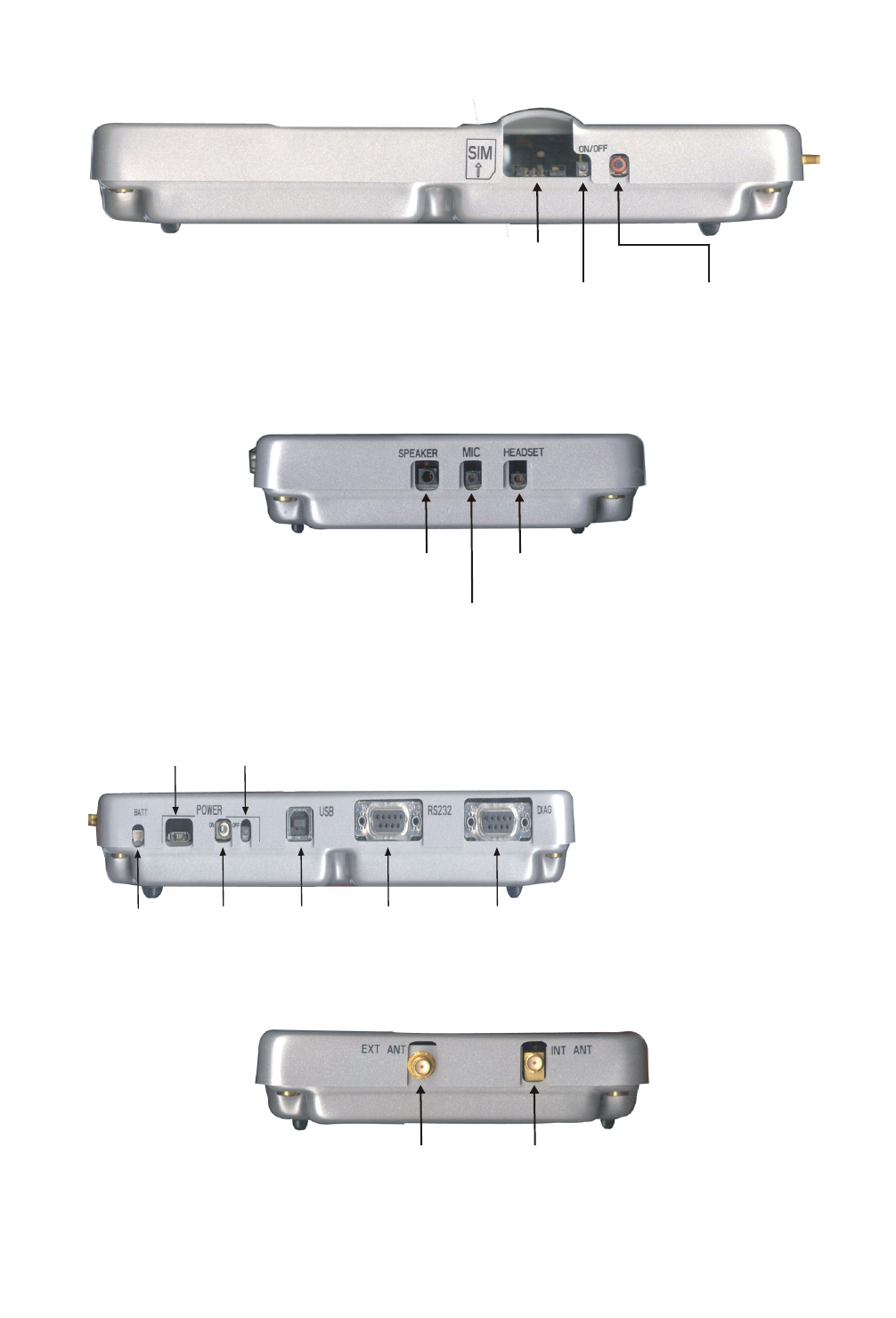
Figure 1. g20 Developer’s Kit (top view, with cover)
On-board Antenna
SIM Tray
KeypadDisplay
8 98-08901C67-D
Figure 2. g20 Developer’s Kit (front, with cover)
Figure 3. g20 Developer’s Kit (left side, with cover)
Figure 4. g20 Developer’s Kit (rear, with cover)
Figure 5. g20 Developer’s Kit (right side, with cover)
SIM Tray
g20 On/Off
Pushbutton
g20 Power
Indicator LED
Speaker
Connector
Microphone
Connector
Headset
Connector
Power Adapter
Connector
Power
On/Off Switch
USB
Connector
RS232-1
Connector
Diagnostics (RS232-2)
Connector
Battery Connector
Power
Indicator LED
External
Antenna Input
Internal
Antenna Input
98-08901C67-D 9
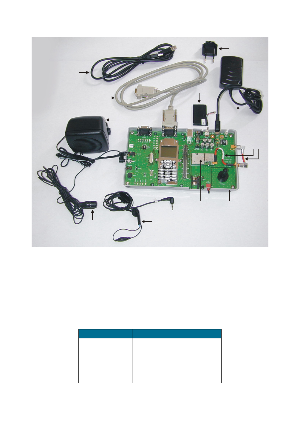
2.2 PACKAGE CONTENTS
The g20 Developer’s Kit includes the Developer Board, chassis and cover, as well as accessories that enable you to better utilize
the board. The kit contains the following components:
Kit Number: F3030B
Table 2. g20 Developer’s Kit Package Contents
Part No. Description Quantity
FTN8121C Developer Board 1
NNTN4250B Wall Mount Power Adapter 1
SYN7456A European Plug for Adapter 1
8102316T02 Test SIM Card 1
SYN6962A Mono Headset w/Detect 1
3087563V12 USB Cable 1
3087563V13 RS232 Cable 1
2987604U01 DC Power Input Mount — VCC 1
2987604U02 DC Power Input Mount — GND 1
0310907A03 M2/6mm Screw (for g20 fastening) 2
8509397T03 Antenna Stub 1
1587867V01 Developer Board Chassis 1
1587867V02 Developer Board Cover 1
3087568V01 RF cable between internal antenna
and external connectors
1
3087568V02 RF cable with MMCX connector
between g20 and external antenna
connector
1
FVN5245A Documentation CD 1
SVN4651A Software CD 1
10 98-08901C67-D
Figure 6 shows the g20 Developer’s Kit, including the Developer Board (without cover) and the g20 and some accessories
attached.
Figure 6. g20 Developer’s Kit with Accessories and the g20
The Developer’s Kit does not include a g20 device. A g20 must be obtained separately.
2.3 ACCESSORIES
Table 3 provides a list of additional accessories for the Developer’s Kit, which are sold separately.
Table 3. Accessories Sold Separately
Part No. Description
0189727L01 3.6V Lithium-Ion Battery
0187506V08 Host Interconnect Flex Cable
FSN5527A Audio Speaker 8
SYN5708A Audio Microphone (Passive)
SYN7455A UK Plug for Adapter
g20 Developer Board
Headset
RS232 Cable
USB Cable
Microphone
Power Adapter
RF
Cables
Battery
Speaker
Adapter Plug
Ω

98-08901C67-D 11
3. DEVELOPER BOARD AND
INTERFACES DESCRIPTION
3.1 HOW THIS CHAPTER IS ORGANIZED
This chapter contains the following sections:
•Overview provides an overview of the Developer Board.
•Initial Setup describes how to set up and prepare the Developer Board for first-time use.
•Configuration describes how to modify the default settings to control the operation of the Developer Board.
•Components and Specifications lists each connector, switch, jumper, Dip switch and LED and provides other details and
specifications for the Developer Board.
3.2 OVERVIEW
The g20 Developer Board is designed to support the hardware and software development and validation of the g20 GSM/GPRS
data module. The Developer Board provides a peripheral platform to operate the g20 as a standalone product, and to easily
access the g20’s 70-pin interface connector signals.
The Developer Board has the following functions:
• Serves as a mounting platform for the g20 module
• Supplies the g20 module with power
• Provides standard communication interfaces (USB and RS232) to the g20
3.2.1 Developer Board Features
The Developer Board provides the following features to facilitate software and hardware development:
• Easy access to the g20’s 70-pin interface connector signals, through a large header connector and an external host connector
• AC, battery and DC power supplies for board operation
• LED indicators for critical signals
• Display and keypad for phone operation
• USB and RS232 serial interfaces
• Diagnostics interface for g20 debugging (RS232-2)
• Digital audio interface
• Analog audio interface for speaker, alert transducer, microphone and headset
• SIM card connector
• Switches and jumpers for controlling board operation
12 98-08901C67-D
3.2.2 Developer Board Components
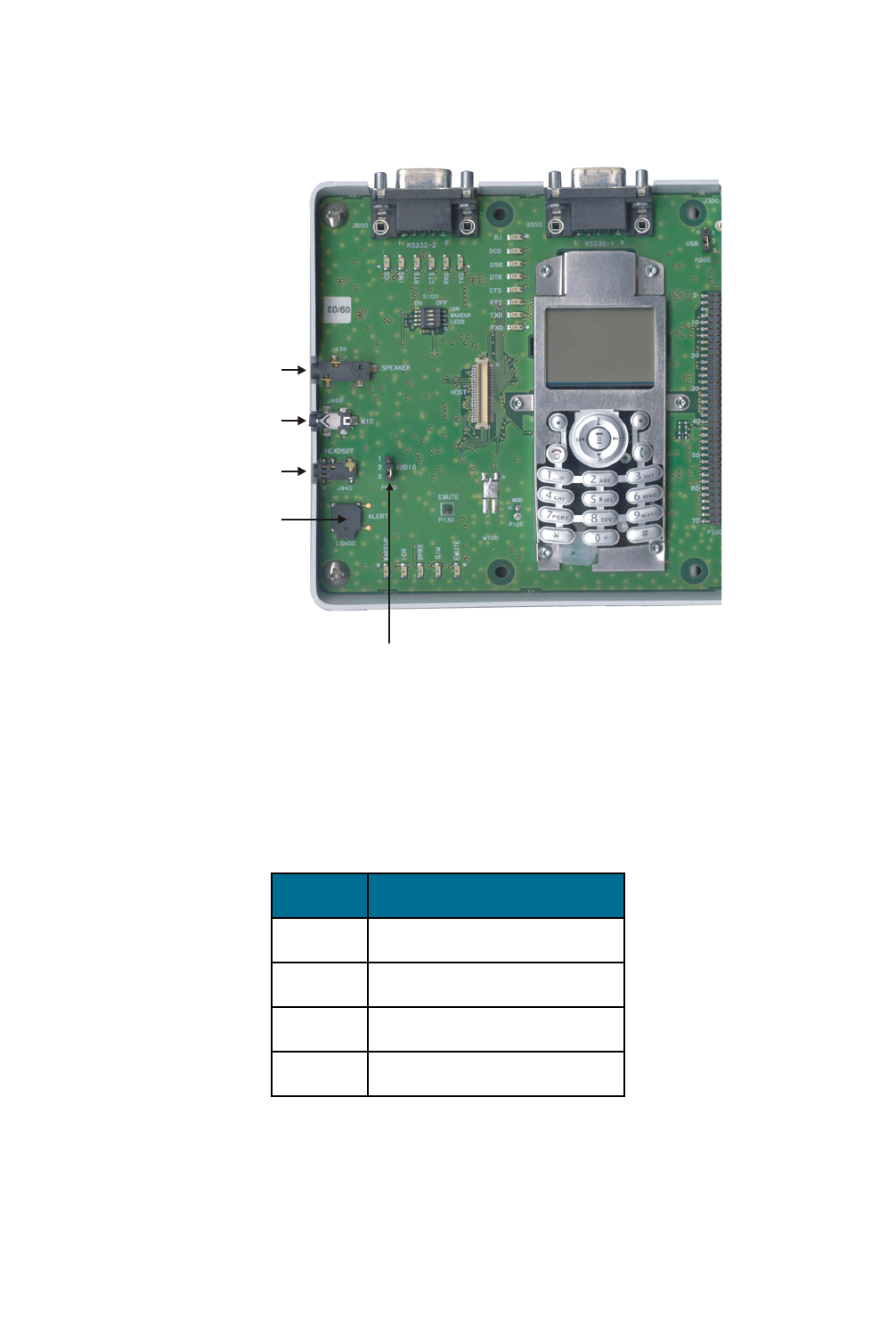
Figure 7 shows the Developer Board and its components:
Figure 7. Developer Board Components
Diagnostics (RS232-2)
Connector
SPI and
RS232-2
LEDs
Dip
Switches
Speaker
Connector
Microphone
Connector
Headset
Connector
Alert
Transducer
GPIO
LEDs
g20 On/Off
Pushbutton
g20 Power
Indicator LED
Internal
Antenna
Internal
Antenna
Input
External
Antenna
Input
g20 UUT
Connector
Power Jumpers
USB
LEDs
Host
Connector
Power Source
Jumper
SIM Card
Detect Logic
Jumper
g20 Header
Connector
MMI Keypad
& Display
SIM Card
Tray
Entertainment Mute
Input Jumper
Audio
Jumper
RS232-1
Connector
RS232-1
LEDs
Battery
Connector
Power
Adapter
Connector
DC Power
Connectors
Power
Indicator LED
USB
Connector
Fuse
2.5A
USB
Jumper
Power On/Off
Switch
Off On
98-08901C67-D 13
3.3 INITIAL SETUP
This section describes the initial procedure for setting up the g20 Developer Board for testing and evaluating of the g20. The
tasks in this section need to be performed only once, before the first time you use the g20 Developer’s Kit. After performing the
initial setup, you can modify the default settings or use different peripheral devices, as described in “Configuration” on page 16.
Perform the steps in this section in sequence.
Before starting, remove the cover of the Developer Board. The cover simply slides up off the board, and does not require the
removal of any screws or clips. After setting up the Developer Board, you can place the cover back on the Developer Board by
simply pushing it gently back into place. Make sure the cover is aligned properly with the external connectors on the side of the
board.
3.3.1 g20
The Developer Board works with all versions of the g20. There are four versions of the g20:
• European version
• European version with USB driver
• North American version
• North American version with USB driver
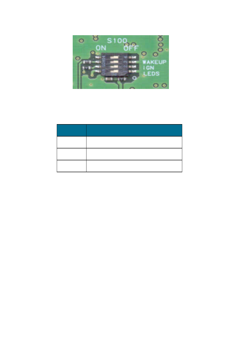
Connect the g20 to the Developer Board by performing the following steps:
• Place the g20 into the area on the Developer Board marked by a white rectangle, and push the g20 70-pin connector down
into the UUT 70-pin connector (P1). The two screw holes on the g20 should be aligned with the g20 spacers (M2 and M3).
• Fasten the g20 to the Developer Board using the two M2 screws provided with the kit.
Figure 8. Connecting the g20
External Antenna
Connector
RF
Cable
MMCX
Connector
g20
Screws
Internal Antenna
Connector
RF Cable
g20
14 98-08901C67-D
• An RF cable with an MMCX connector is connected to the external antenna connector. Connect the RF cable’s MMCX
connector to the MMCX connector of the g20 by pushing it in until it clicks. This connects the g20 to the antenna.
3.3.2 External Connectors
Place the cover back on the Developer Board and connect the following external connectors.
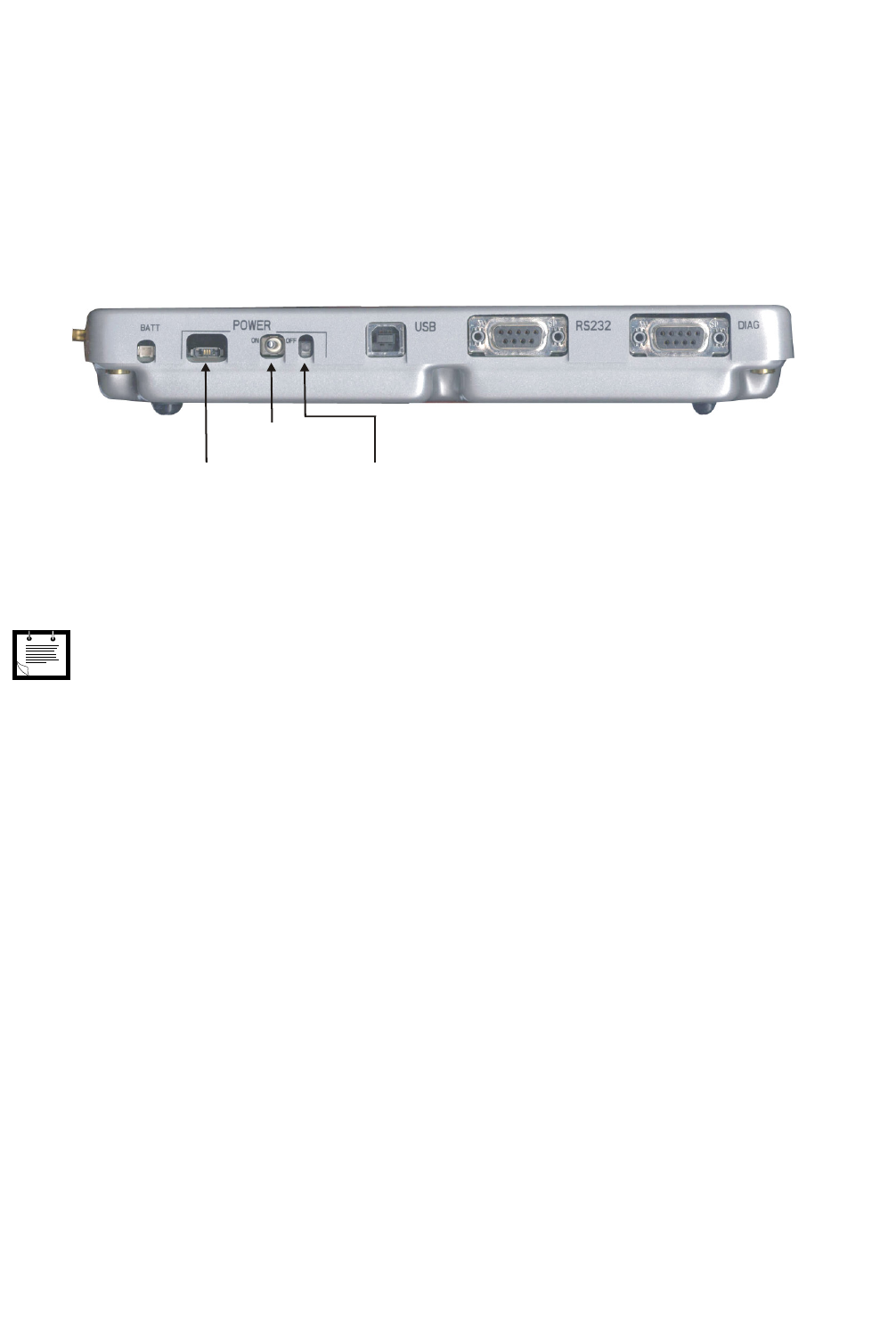
3.3.2.1 Power Supply
Make sure the Developer Board power switch is off before connecting the power supply.
Figure 9. Developer Board Power Switch and Adapter Connector
Connect the supplied power adapter to the Developer Board adapter connector (J230), which is labeled Power on the cover of
the Developer Board. Plug the adapter into a wall outlet.
3.3.2.2 PC Connection
USB and RS232 serial interfaces are available for PC communications. If a PC connection is required, connect either a RS232
cable with a male D-type connector to the RS232 connector (J350), or a USB cable with a B-type connector to the USB
connector (J300).
The g20 Developer’s Kit includes the necessary RS232 and USB cables.
Note
The g20 Developer Board can also be powered by an external DC power supply or battery cell. These options are
described in “Configuration” on page 16.
Power Adapter
Connector
Developer Board
On/Off Switch
Power Indicator
LED
98-08901C67-D 15
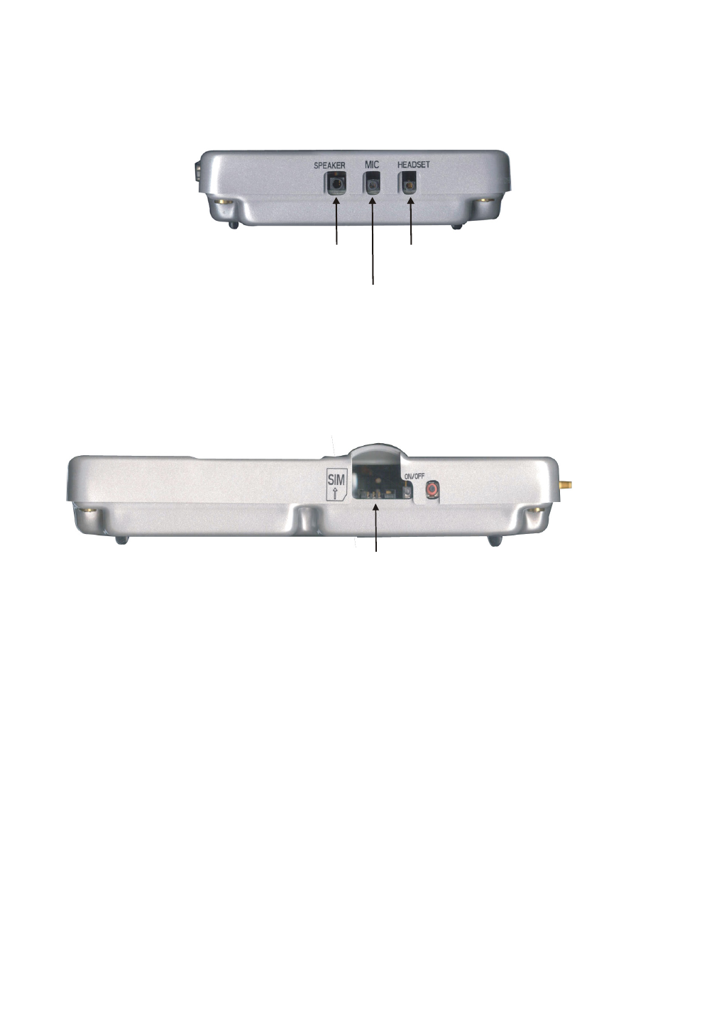
3.3.2.3 Audio Devices
If you wish to use the audio capabilities of the g20, you may connect the supplied headset, which includes a speaker and
microphone. The headset connector is labeled HEADSET and is located on the left side of the Developer Board, along with
connectors for additional audio devices.
Figure 10. Audio Connectors
3.3.2.4 SIM Card
Insert a SIM card into the SIM tray (J100) with the contacts down and the cut-off corner to the front and right. A diagram on the
cover indicates how to insert the SIM.
Figure 11. SIM Tray
A test SIM card is provided with the g20 Developer’s Kit.
3.3.2.5 Antenna
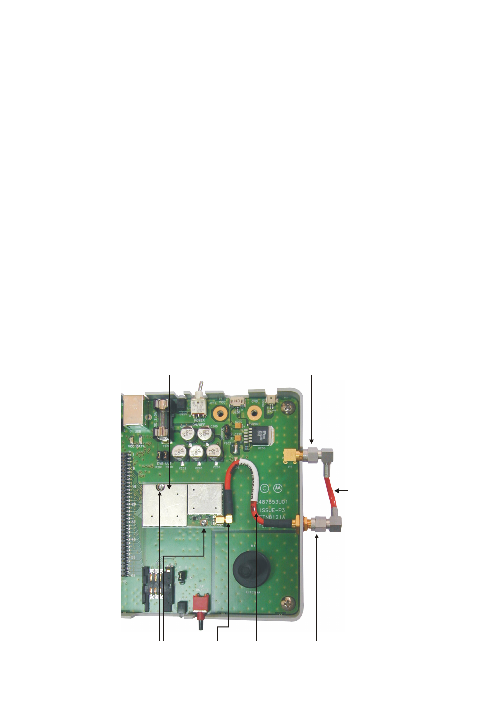
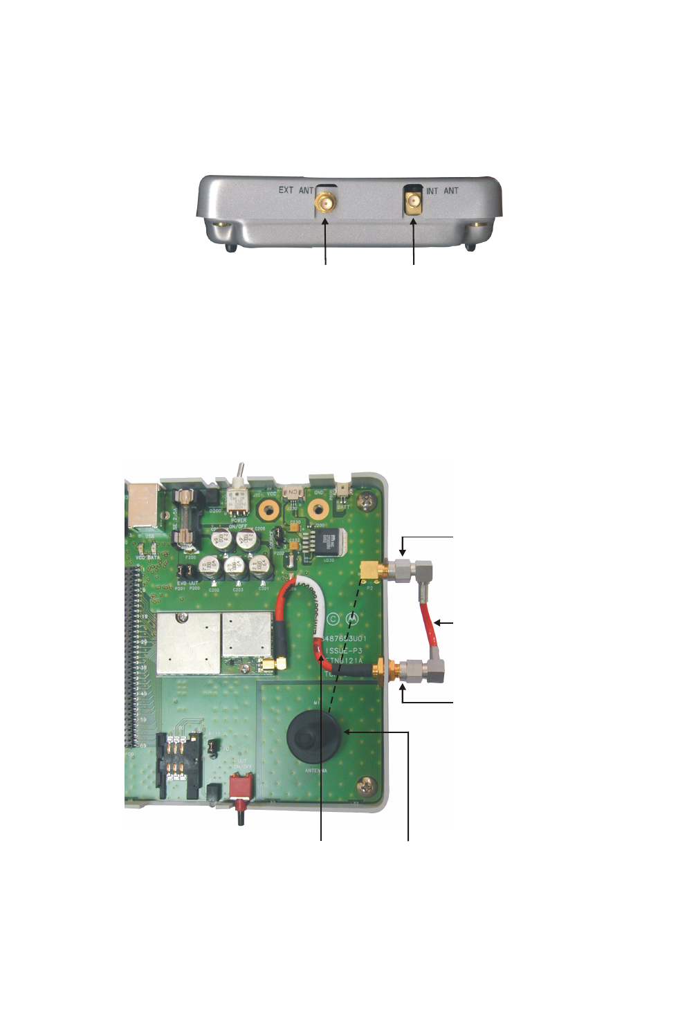
Attach the supplied antenna stub by screwing it in to its base, on top of the Developer's Kit.
The Developer's Kit arrives configured to operate with its on-board internal antenna. The EXT ANT and INT ANT antenna
connectors are connected together through an external RF cable, on the board's right side.
3.3.2.6 Power Up
You must turn on the Developer Board power and then turn on the g20.
• Turn on the Developer Board power by switching on the power switch (S200). The Developer Board power indicator LED
is lit.
• Turn on the g20 by pushing in the g20 on/off switch (S110), holding it in for about a second and then releasing it. You can
also turn on the g20 by pressing and holding the red function button on the keypad. (The red button also functions as the end-
call button.) The g20 on/off LED is lit and the display above the keypad shows text.
The Developer Board is now ready for use.
Speaker
Connector
Microphone
Connector
Headset
Connector
SIM Tra
y
16 98-08901C67-D
3.4 CONFIGURATION
After performing the initial setup in the previous chapter, you can use the Developer Board with the default setup. This section
describes how to change this setup in order to use different peripherals or to change the way the board operates.
3.4.1 Alternate Power Sources
Developer Board power can be supplied from an AC power adapter, external DC power source or battery. The same power
source is used for the g20 and the board peripherals.
You must connect the Developer Board to a power source, and then set the power source jumper (P202), if necessary.
There are two other jumpers that help control the power supply in the Developer Board:
•P201: Connects/disconnects the power from the Developer Board peripherals
•P200: Connects/disconnects the power from the g20
Figure 12. Power Supply Connectors, Jumpers and Switches
Each power supply option is described in the sections that follow.
Battery Connecto
r
Power Adapter
Connector
P202
(Power Source
Jumper)
DC Power
Connectors
P200
(g20 Power
Jumper)
P201
(Developer Board
Power Jumper)
98-08901C67-D 17
3.4.1.1 AC Adapter Operation
When using an AC adapter, the adapter is connected to the power adapter connector (J230). The adapter supplies a constant
4.5 V, which is regulated to a nominal 4.1 V on the Developer Board.
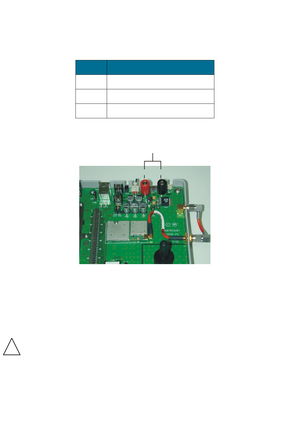
3.4.1.2 DC Power Source Operation
You can use an external DC power supply by connecting it to the VCC (J201) and GND (J200) connectors.
Figure 13. DC Power Connectors
The supplied DC input connectors must be attached to the Developer Board in order to use an external DC power source. Use
the red connector for VCC and the black one for GND. Connect the DC power source to these connectors using banana plugs,
alligator clips or wire.
The DC voltage applied through this connection should not exceed the recommended operational limits of 3 V to 4.2 V. In all
cases, the DC source input is protected from over voltage and reverse polarity, and includes a 2.5A protective fuse.
When using the DC power input connectors, the Developer Board cover must be removed.
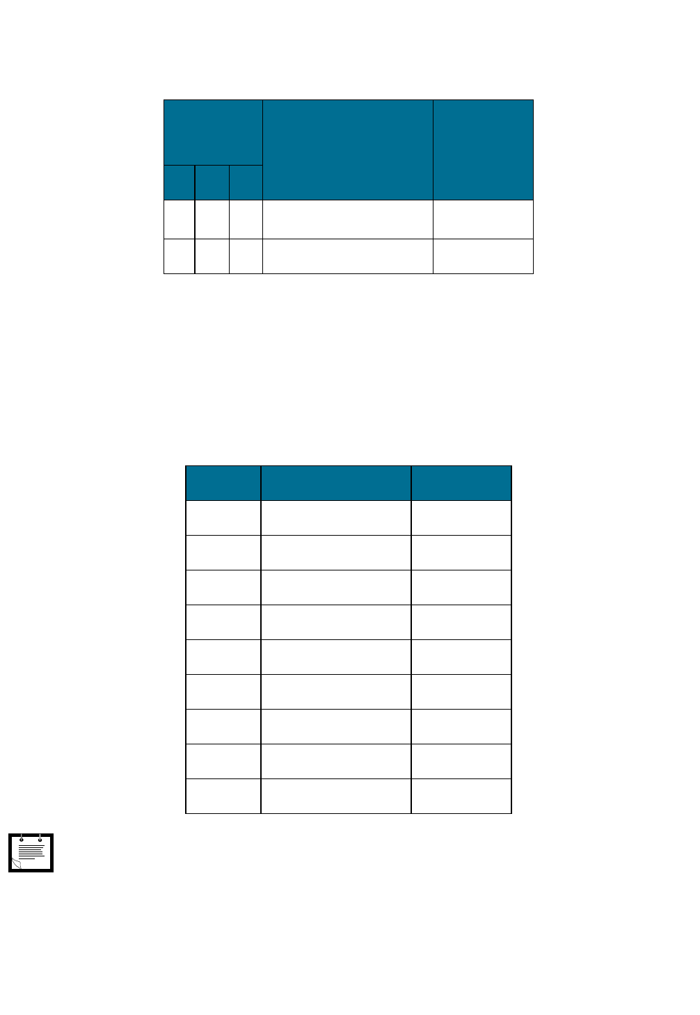
Table 4. Power Adapter Connector Pinout (J230)
Pin # Pin Name
1GND
2 Detection circuit
3VCC
!
Caution
It is recommended to remove jumper P202 when using the DC power source. The DC power source should not be
used when other sources are connected.
VCC GND
DC Power Connectors
18 98-08901C67-D
3.4.1.3 Battery Operation
The Developer Board supports a battery power supply. The battery used must be a 3.6V lithium-ion cell, corresponding to
Motorola part number 0189727L01. The battery is an optional accessory.
When using a battery as the main power source, the AC adapter input operates as a battery charger, which connects to an
on-board battery charging circuit.
3.4.1.4 Power Source Selection
The Developer Board AC adapter and battery power inputs include a selection jumper (P202) that diverts either the regulated
AC adapter power or the battery power to the board.
Jumpers are provided for disconnecting the power from the Developer Board and for disconnecting the power from the g20.
You may wish to remove the Developer Board power jumper and shut off the power to the board in order to diagnose a problem
that may be caused by the board. The g20 will continue to receive power..
Table 5. Battery Connector Pinout (P600)
Pin # Pin Name
1VCC
2GND
Table 6. Power Source Jumper (P202)
P202 Jumper
Position Selected Mode Power Source
1 2 3
•• Adapter AC Adapter
••Battery Li-Ion Battery
Adapter and battery disconnected DC power only
Table 7. Developer Board Power Jumper (P201)
P201
Jumper
Position Selected Mode
1 2
••Developer Board connected to
power source
Developer Board disconnected
from power source
98-08901C67-D 19
You may also want to remove the g20 power jumper and then connect an amperometer to the jumper’s two pins to measure the
current through the g20.
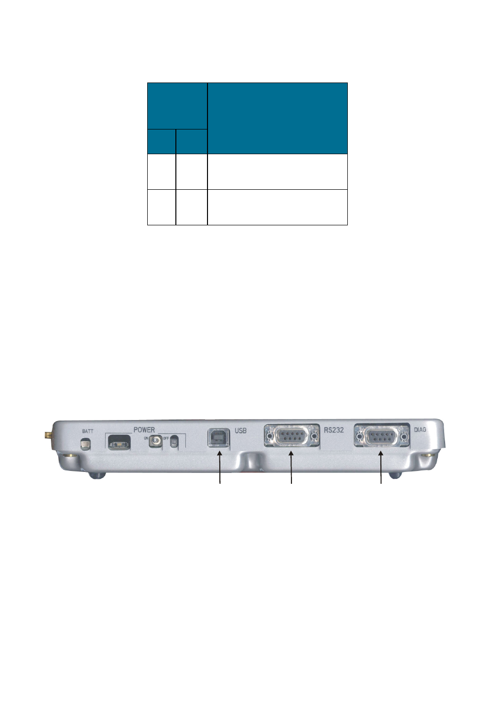
3.4.2 Communication Interfaces
The g20 Developer Board includes three serial interfaces:
• RS232
•USB
• Diagnostics
The RS232 and USB ports are multiplexed within the g20, and therefore cannot be operated simultaneously. The default
connection is RS232.
The USB and RS232 is not detected dynamically. The selected serial connection is determined by the USB cable connection at
power up. If the USB cable is connected (and the PC is on), then USB is selected. Otherwise, RS232 is selected.
The Diagnostics RS232 interface is used for debugging.
Figure 14. USB, RS232 and Diagnostics Connectors
Each of these serial interfaces is described in the sections that follow.
Table 8. g20 Power Jumper (P201)
P200
Jumper
Position Selected Mode
1 2
••g20 connected to power
source
g20 disconnected from power
source
USB
Connector
RS232-1
Connector
Diagnostics (RS232-2)
Connector
20 98-08901C67-D
3.4.2.1 RS232
The 9-pin, D-type RS232-1 serial port (J350) is the primary interface to the g20 UUT. The UUT RS232 signals are active-low
CMOS-level signals (0-2.7 V), which are converted by the Developer Board to standard RS232 levels for PC communications.
3.4.2.2 USB
The USB interface connector (J300) is a standard B-type USB device interface. The g20 USB signals are routed directly to this
connector. The Developer Board includes a USB driver circuit, similar to the g20’s internal USB circuit, for reference and
testing purposes only. For proper USB communications, the Developer Board’s USB driver should not be used.
Table 9. RS232-1 Connector Pinout (J350)
Pin # Description DTE I/O
1 DCD In
2RXD In
3TXD Out
4DTR Out
5 Ground
6DSR In
7RTS Out
8CTS In
9RI In
Note
The RS232-1 connector pin names are DTE-oriented.
Table 10. USB Connector Pinout (J300)
Pin # Description
1VCC
2D-
3D+
4 Ground
98-08901C67-D 21
3.4.2.3 Diagnostics
The 9-pin D-type Diagnostics serial port (J500) is connected to the g20 internal SPI bus. This interface is used to debug appli-
cations.
On the Developer Board, the g20 SPI interface is converted to standard RS232 signals for PC communications. The conversion
process uses the RS232 interface as a second slave on the internal g20 SPI bus, and communicates with it as such. SPI read and
write operations are performed normally, using the CS and IRQ signals provided by the conversion circuit. The IRQ signal is
connected to a g20 IRQ pin.
Table 11. USB Jumper (P300)
P300
Jumper
Position Selected Mode USB Source
1 2 3
•• g20 g20 driver
USB disconnected
Note
The RS232-2 connector pin names are DTE-oriented.
Table 12. Diagnostics Connector Pinout (J500)
Pin # Description DTE I/O
1 Unused
2RXD In
3TXD Out
4 Unused
5 Ground
6 Unused
7RTS Out
8CTS In
9 Unused
22 98-08901C67-D
3.4.3 Audio Interface
The Developer Board includes analog and digital audio interfaces. The audio interface contains a hands-free speaker and
microphone, a headset, and an alert transducer.
Figure 15. Audio Connectors and Jumper
3.4.3.1 Speaker
The differential speaker interface is designed as a hands-free speaker. The Developer Board uses an audio amplifier to amplify
the speaker audio output to desired levels. The speaker connector (J430) is labeled SPEAKER. The speaker output is 8 ohms
matched.
Table 13. Speaker Connector Pinout (J430)
Pin # Description
1 Not connected
2 Speaker positive output
3 Speaker negative output
4 Not connected
Audio Jum
p
er
Speaker
A
lert Transducer
Microphone
Headset
98-08901C67-D 23
3.4.3.2 Microphone
The microphone interface is designed as a hands-free microphone. The microphone connector (J460) is labeled MIC.
3.4.3.3 Audio Source Selection
Microphone and speaker audio can be routed through two different sources: the g20 audio amplifiers or the g20 digital audio
interface. The Developer Board includes a CODEC that converts the g20 digital audio data to analog audio signals.
The P420 jumper, labeled AUDIO, selects the speaker and microphone source, as indicated in Table 15. This enables you to test
the digital or analog audio channels.
Table 14. Microphone Connector Pinout (J460)
Pin # Description
1 Ground
2 Microphone audio-in
3 Ground
4 Ground
5 Ground
Table 15. Audio Jumper (P420)
P420 Jumper
Position Selected Mode USB Source
1 2 3
•• Digital audio CODEC audio I/O
••Analog audio g20 audio I/O
Audio disconnected
24 98-08901C67-D
3.4.3.4 Headset
The headset interface is designed as a portable phone audio interface, and is similar to a phone headset interface. The headset
connector (J440), labeled HEADSET, includes a speaker, microphone and a detection signal. The speaker and microphone
signals are directly connected to the g20 audio signals.
The purpose of the detection circuit is to switch the g20 headset audio paths on and off, whenever a headset connection is
detected. Headset detection is made whenever a headset plug is inserted into the jack. This action disables the g20 microphone
and speaker, and routes the audio signals to the headset.
3.4.3.5 Alert Transducer
The Developer Board includes an on-board transducer, labeled ALERT, for alert audio sounds (LS400). The transducer is
connected directly to the g20 differential alert outputs. The alert transducer sounds the g20 MIDI signals.
Table 16. Headset Connector Pinout (J440)
Pin # Description
1 Ground
2 Headset-detect switch
3 Speaker audio-out
4 Microphone audio-in
5 Ground
Table 17. Alert Transducer Pinout (LS400)
Pin # Description
1 Alert audio inverted output
2 Alert audio positive output
3 Alert audio inverted output
4 Alert audio inverted output
98-08901C67-D 25
3.4.4 Antenna
An antenna (internal or external) must be connected to the Developer Board for adequate GSM reception. You can connect the
g20 to either the on-board internal antenna or to an external antenna.
Two RF connectors on the side of Developer Board, labeled INT ANT and EXT ANT on the cover, are used for setting up the
antenna.
Figure 16. Antenna Connectors (external)
On the inside of the Developer Board, the EXT ANT connector is connected to the g20 and the INT ANT is connected to the
on-board internal antenna.
You must perform one of the following:
• To use the internal antenna, connect the EXT ANT and INT ANT connectors with the additional RF cable supplied in the
Developer’s Kit. This is the Developer Board’s default configuration. It arrives with the EXT ANT and INT ANT already
connected.
Figure 17. Antenna Connectors (internal)
• To use an external antenna, connect an external antenna or antenna application to the EXT ANT connector. (The connection
cable is not included.) You must first disconnect the external RF cable from the EXT ANT connector.
External
Antenna Input
Internal
Antenna Input
On-board
Internal Antenna
g20 RF Cable
Additional
RF Cable
EXT ANT
INT ANT
26 98-08901C67-D
3.4.5 Option Switches
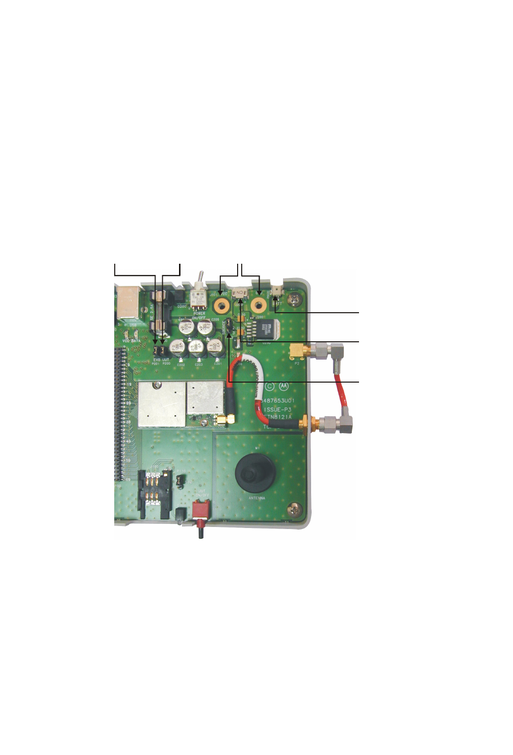
Figure 18 shows the Dip switches provided on the Developer Board, which are located on the S100 component.
Figure 18. Option Switches
The following Dip switches are provided:
3.4.5.1 Wakeup
The WAKEUP switch is connected to the g20’s internal wakeup interrupt module through the WAKEUP_IN_N signal. This
line should be in the off position to enter Sleep mode and in the on position to wake up.
Generally, your application wakes up the g20. In cases where the application is not ready for integration, you can force wakeup
of the g20 by turning on this Dip switch.
3.4.5.2 Ignition
The IGN switch activates the g20 ignition circuits through the IGN signal. You can use this switch to turn the g20 on and off.
3.4.5.3 LEDs Control
The Developer Board includes LED indicators for critical signals.
The LED switch enables you to turn off all the LEDs on the Developer Board, for example, to reduce power consumption. The
Developer Board power on/off LED and the g20 on/off LED are always active and cannot be disabled.
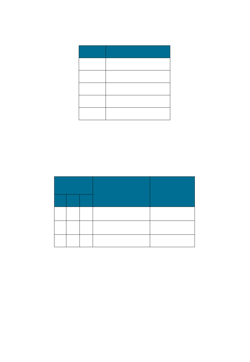
Table 18. Option Switches
Reference Description
WAKEUP g20 wakeup signal
IGN g20 ignition circuit
LEDS on/off switch for LEDs
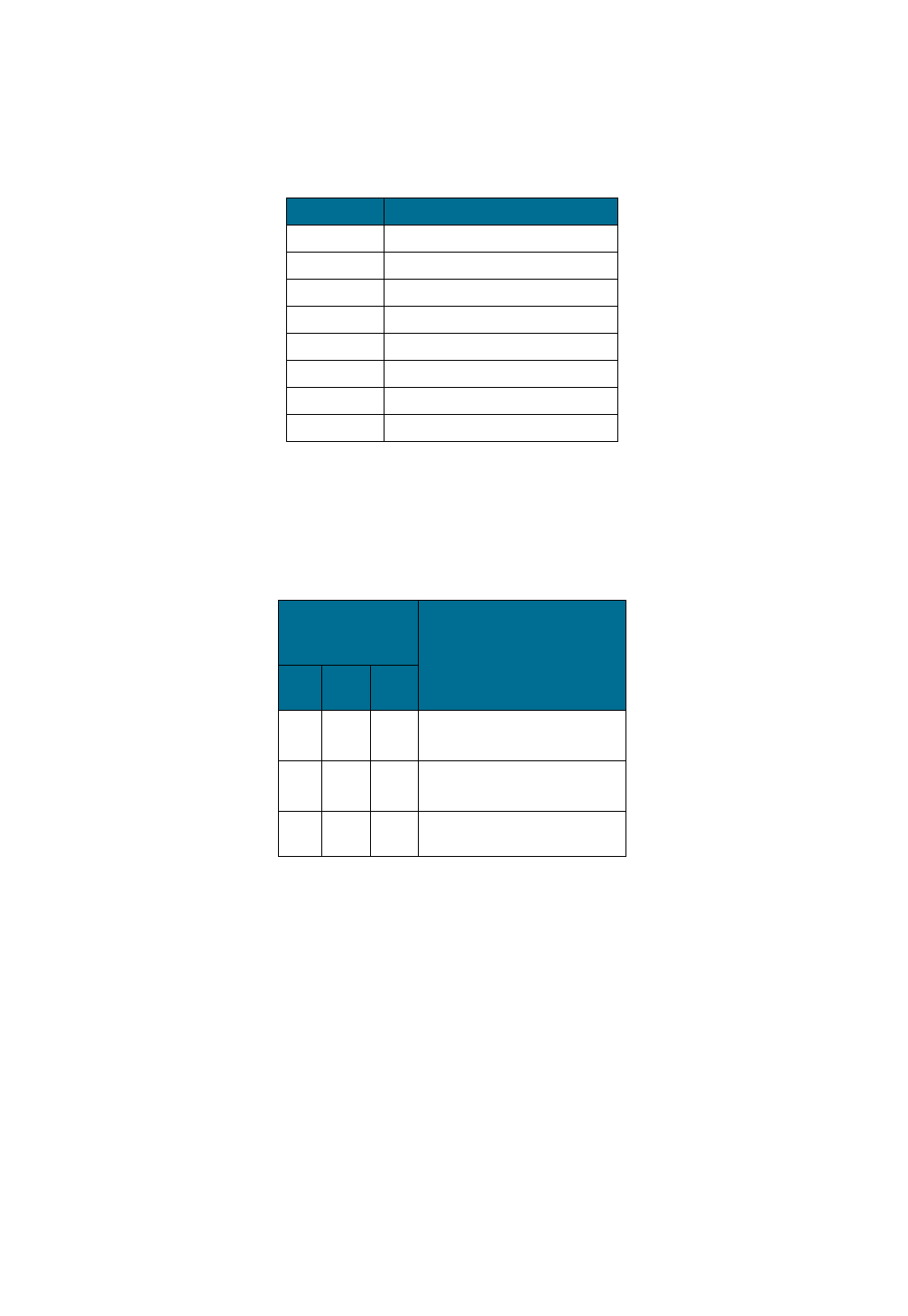
98-08901C67-D 27
3.4.6 SIM Card
The SIM card connector (J100) is external to the g20, but is connected directly to it, similar to an internal SIM. The g20 can
accept 1.8V and 3V SIM cards.
The g20 detects the presence of the SIM card through the SIM_PD signal. This signal is configured in the g20 as active-low.
The Developer Board is configured to support the g20's default active-low detection, but can also support active-high detection,
if necessary. Use the SIM card detect logic jumper (P110), labeled SIM, to select active-low or active-high SIM card detection
configurations.
Table 19. SIM Connector Pinout (J100)
Pin Description
1 Ground
2 Presence detect
3Clock
4Reset
5VCC
6 Serial data I/O
7 VPP
8 Ground
Table 20. SIM Card Detect Logic Jumper (P110)
P110 Jumper
Position Selected Mode
1 2 3
•• Active-low
••Active-high
Not active
28 98-08901C67-D
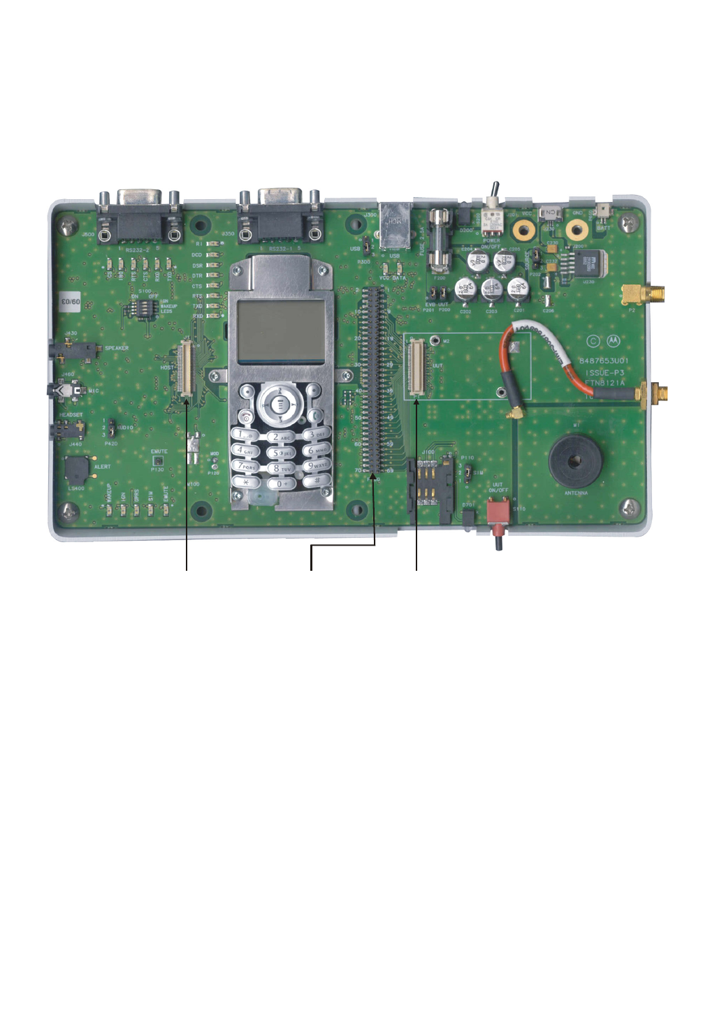
3.4.7 Host Connection
An external application may communicate with the g20 through the host connector (J1) and control some or all of the g20's
functions. The host connector enables you to integrate the g20 into an application without installing the g20 inside the product.
The host connector operates in parallel with the developer board peripherals and enables an external application to share g20
resources with the developer board. You may select any g20 function to control externally, through the host connector, and allow
the developer board to control other functions.
Figure 19. 70-pin Connectors
You can connect an external application to the g20 Developer Board using a host interconnect flex cable and connecting it to
the host connector (J1). Connect the other end of the cable to the external application. The cable is an optional accessory.
All pin numbers and functions of the host connector are identical to those of the g20 UUT (P1) and the g20 diagnostic connector
(P100). For more information on the pins of the host connector, refer to “UUT Interface Connector” on page 30.
The following are guidelines for using the host connector:
• When using an external SIM card through the host connector, the developer board SIM card jumper (P110) must be discon-
nected and the SIM card tray should be empty.
• When using any of the serial communication channels (USB, RS232, SPI) through the host connector, the developer board
serial connectors should not be used.
• When using the IGN or WAKEUP functions through the host connector, the functions should be switched off on the devel-
oper board Dip switches.
• When using the analog audio channels through the host connector, disconnect all audio devices from the developer board.
• When using the PCM digital audio through the host connector, it is recommended to place the audio selection jumper (P420)
to analog audio mode.
• When connecting an external application that provides the power to the g20 and the Developer Board, remove any other
power sources from the Developer Board.
g20 70-pin
Connector
70-pin
Host Connector
g20 70-pin
Header Connector
98-08901C67-D 29
3.5 COMPONENTS AND SPECIFICATIONS
3.5.1 Connectors Description
All the Developer Board connectors are marked by their reference number and by a pin-1 indicator. Table 21 describes the avail-
able connectors on the Developer Board.
Table 21. Connectors
Reference Connector Description
Internal Connectors (not visible when cover is on)
P1 g20 UUT g20 UUT (unit under test) connector
J1 Host Emulates the g20 connector for host systems
P100 Header Debug header connector (70-pin)
J201 VCC Developer Board DC power supply
J200 GND Developer Board common ground
External Connectors (visible when cover is on)
J300 USB USB B-type connector
J350 RS232-1 Primary RS232 to PC
J500 RS232-2 Secondary RS232 for debugging (Diagnostics)
J430 Speaker Hands-free system speaker jack
J460 Microphone Hands-free system microphone jack
J440 Headset Headset jack
P600 Battery Battery connector
J230 AC adapter/charger Wall-mount adapter connector
J100 SIM card SIM card socket with detection
P2 Antenna connector SMA connector for internal antenna
M1 RF Antenna Internal antenna
30 98-08901C67-D
3.5.1.1 UUT Interface Connector
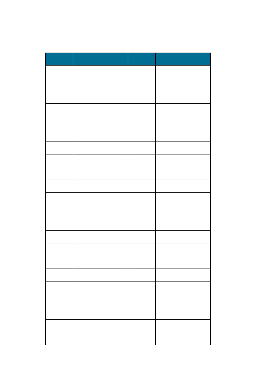
Table 22 lists the pin names and functions available for the g20 interface connectors. All pin numbers and functions are identical
to the g20 UUT (P1), host (J1) and g20 Diagnostic (P100) connectors on the Developer Board.
Table 22. g20 Connectors Pinout
Pin # Pin Name Pin # Pin Name
1GND 2GND
3GND 4GND
5VCC 6VCC
7VCC 8VCC
9 RTS_N 10 USB_VBUS
11 RXD_N 12 USB_D+
13 DSR_N 14 USB_D-
15 CTS_N 16 WAKEUP_IN_N
17 DCD_N 18 PCM_DIN
19 DTR_N 20 PCM_DOUT
21 TXD_N 22 PCM_CLK
23 RI_N 24 PCM_FS
25 RESET_N 26 WAKEUP_OUT_N
27 BL_SINK 28 KBC1_N
29 CHRG_DIS 30 KBC0_N
31 CHRG_SW 32 KBR0_N
33 CHRG_STATE 34 KBR1_N
35 CHRG_DET_N 36 KBR2_N
37 Not connected 38 KBR3_N
39 TX_EN_N 40 KBR4_N
41 ANT_DET 42 KBR5_N
43 VIB_OUT 44 SIM_RST_N
98-08901C67-D 31
45 CHRG_TYP 46 SIM_CLK
47 THERM 48 SIM_VCC
49 GPRS_DET_N 50 SIM_PD
51 IGN 52 SIM_DIO
53 ON_OFF_N 54 LCD_CS
55 HDST_INT_N 56 LCD_DATA
57 HDST_MIC 58 LCD_CLK
59 MIC_GND 60 LCD_RS
61 MIC 62 SPI_IRQ_N
63 ALRT_N 64 SPI_DIN
65 ALRT_P 66 SPI_CLK
67 SPKR_N 68 SPI_DOUT
69 SPKR_P 70 SPI_CS
Table 22. g20 Connectors Pinout (Continued)
Pin # Pin Name Pin # Pin Name
32 98-08901C67-D
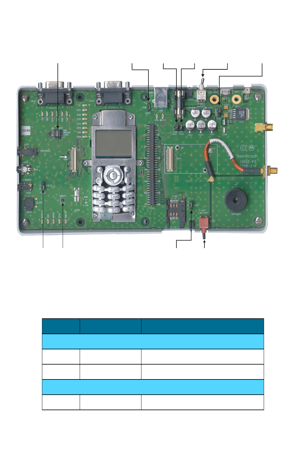
3.5.2 Switches and Jumpers
Figure 20 shows the jumpers and switches on the Developer Board.
Figure 20. Jumpers and Switches on Developer Board
Table 23 describes the available switches and jumpers on the Developer Board.
Table 23. Switches and Jumpers
Reference Switch/Jumper Description
Switches
S200 Board on/off Developer Board on/off switch
S110 g20 on/off g20 on/off pushbutton switch
Dip Switches
S100 Option switches Four switches for Developer Board options
P420
(Audio)
P130
(EMUTE)
P110
(SIM)
S110
(g20 On/Off
Pushbutton
)
Host
Connector
P200
(g20 Power)
S200
(Power On/Off
Switch)
P202
(Power Source)
S100
(Option Switches)
P201
(Developer
Board Power)
P300
(USB)
98-08901C67-D 33
Jumpers
P420 Audio Analog/digital audio-selection jumper
P201 EVB Peripheral power input jumper
P200 UUT g20 UUT power input jumper
P202 Source Power source selection jumper
P110 SIM SIM card detect logic selection jumper
P300 USB USB driver jumper (not used)
Table 23. Switches and Jumpers (Continued)
Reference Switch/Jumper Description
34 98-08901C67-D
3.5.3 LED Indicators
Figure 21 shows the LEDs on the Developer Board.
Figure 21. LEDs on Developer Board
Table 24 describes the LED indicators on the Developer Board. Each LED is marked on the board by the function it represents.
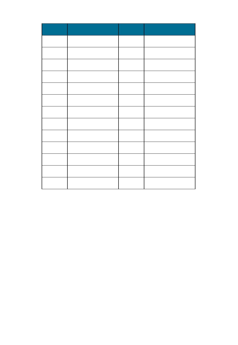
Table 24. LEDs
Group LED Reference Description
GPIO
WAKEUP D704 Wake-up in/out
IGN D702 Ignition input
GPRS D710 GPRS coverage indication
SIM D703 SIM card reset indication
EMUTE D708 Not used
Power
UUT D701 g20 on/off
PWR D200 Power
GPIO
LEDs
g20 On-Off
Host
Connector
SPI
LEDs
RS232-2
LEDs RS232-1
USB
LEDs
Developer
Board Power
98-08901C67-D 35
SPI
CS D741 SPI chip-select output
IRQ D744 SPI IRQ input
USB
VCC D760 USB VBUS
DATA D761 USB D+
RS232-1
RXD D722 DTE receive data
TXD D721 DTE transmit data
RTS D724 Request to send
CTS D723 Clear to send
DTR D725 Data terminal ready
DSR D726 Data set ready
DCD D727 Carrier detect
RI D728 Ring indicator
RS232-2
RXD D743 DTE receive data
TXD D742 DTE transmit data
CTS D744 Clear to send
RTS D745 Request to send
Table 24. LEDs
Group LED Reference Description
36 98-08901C67-D
3.5.4 MMI
The Developer Board includes a man-machine interface (MMI), complete with display and keypad. The MMI is intended for
initial operation and evaluation of the g20.
The keypad does not function on generic g20 sales models, a special flex should be requested in order to have the keypad func-
tioning.
For more information on MMI connections, refer to the schematics in “Schematics and Placement Diagrams” on page 55.
3.5.5 AC Adapter Detection Circuit
The g20 charger module includes a detection logic circuit for detecting charger presence and type. The detection circuit is inter-
nal to the g20 module. However, the Developer Board does contain the necessary routing from the g20 UUT to the AC adapter
connector.
Two g20 signals are used for this detection:
•CHRG_TYP: ADC signal for charger type detection
•CHRG_SW: Charger rate control
These detection signals are present to provide compatibility with the phone. They may be removed in future versions.
3.5.6 Electrical Specifications
Table 25 describes the electrical specifications of the Developer Board.
* When using DC power supply only.
** Depends on the active peripherals (LEDs, UART, USB, and so on) in use.
Table 25. Electrical Specifications
Parameter Units Min Typ Max
DC power supply V 3.0 3.6 4.2
Adapter power supply V 4.4 4.6 12
Battery power supply V 3.0 3.6 4.2
Off current*uA 3.6 42.6
On current mA 8.0 8.25 8.45
Active current, peripherals off mA 12.3 12.4 ---
Active current, peripherals on** mA 12.6 --- ---

98-08901C67-D 37
4. SERVICE SUPPORT
4.1 CUSTOMER ASSISTANCE
This section provides contact information for any possible queries that may arise, such as the following:
• Have questions?
• Having trouble getting the Developer Board set up?
• Technical questions?
• Configuration questions/problems?
• Technical operating problems?
• Need documentation?
The GSM/CDMA Data Module Customer Support Center is ready to assist you on integration issues.
A direct customer should use the following email address to contact customer assistance: n2cshd@motorola.com.
An indirect customer should send his requests to his distributor and not to Motorola help desk.
Every new call/problem report should be directed to the help desk email address noted above. It is recommended to report each
individual issue in a separate email. The following information is required when reporting a problem:
• Customer name and address
• Customer contact information for this request, including:
•Name
• Telephone
• Fax number
• Mobile number
• Email address
• Product name (g20)
• Software version of the unit (ATI3 command) or model number
• PCB version. This information is located on the PCB near the RF connector.
• Severity of the problem
• Problem description, including:
• Operator name
• Type of SIM card (for example, Test, Pre-paid, or 5v/3v/1.8v)
• Configuration of the setup (such as Developer Board, handset, host, connections, and so on)
• Detailed scenario from startup
• Log of all the commands and the responses, beginning from startup
Note
The support services provided by Motorola are subject to the agreement between the customer and Motorola and
may be at an additional charge to the customer. Motorola will inform the customer in advance of any such charge.

38 98-08901C67-D
• Answers to the following questions:
• Was the same scenario tested on the Developer Board and the PC to reproduce the problem?
• How many units do you have, and how many of them have this problem?
• How often does the problem recur?
In addition to the information requested above, send the following AT commands and the HyperTerminal log with the
responses:
AT+CMEE=2 // To get textual error message
AT+CPIN? // To get SIM card status
AT+CREG? // To see if the TXVR is registered to the network
AT+CSQ // To get the signal strength (RX level)
AT+CGSN // To read the IMEI number of the unit
ATI3 // To get the software version of the TXVR
AT\S // To get the setting of basic AT commands
AT+CMER=0,0,1,1 // To get messages and indicators from the handset display to the DTE
4.1.1 Motorola Workflow
The help desk uses the following workflow when responding to new calls:
1. Each new call is registered in the help desk data base.
2. The help desk immediately notifies the customer with the help desk system record number for each issue.
3. A champion is assigned to be responsible for the new call, from arrival to closing.
4. During this time, the champion updates the help desk system with the progress of the resolution process.
5. The champion is the contact to the customer and the engineering team, and coordinates activities that are required to solve
the problem.
4.1.2 Service Centers
Motorola Electronics Taiwan PCS
11F, No, 296, Sec. 4, Jen-Ai Road
Taipei, 106, Taiwan, R.O.C
Motorola GmbH
Am Sophienhof 10
D-24941 Flensburg
Germany

98-08901C67-D 39
Motorola Communications ISRAEL Ltd.
Service Operation
Attention: Shukrun Ofer
3 Krementsky Street
Tel Aviv, Israel 67899
Telephone: (972) 3 5658829
JNB Electronics Pty Ltd.
347 Settlement Road, Thomastown
VIC 3074
Australia
Field service should be coordinated with the Service Manager in Motorola using the following email address:
N2CSFS01@motorola.com
40 98-08901C67-D
4.2 TROUBLESHOOTING
The following table lists problems that may occur during board operation, and describes how to resolve them. If the problem
persists, please contact your Motorola representative.
Table 26. Troubleshooting
Problem Indication Action
Power
Developer board
does not power up
Power LED does not light Check the power source connection.
If using an external DC power source, verify that the supply
is within the limits of 3.0 V to 4.2 V.
Verify that the board power switch (S200) is on.
Check the source jumper (P202) position.
Verify that the EVB jumper (P201) is present.
Verify that the protective fuse is not burned out.
The g20 does not
power up
The g20 on/off LED doesn’t
light or lights for a short
period
Check the g20 connection to the Developer Board.
Verify that the UUT jumper (P200) is present.
Depress the g20 on/off pushbutton for a longer period.
The g20 on/off LED lights
up automatically when
power is applied
Verify that the IGN option switch is off.
The g20 on/off LED blinks Contact your Motorola representative.
Image freezes on the
display at start up
Contact your Motorola representative.
High current
consumption
The protective fuse
burns out
Check the polarity of the DC power inputs.
Verify that only one optional power source is connected.
GSM Reception
No GSM reception
available
The g20 unit searches
unsuccessfully for network
Verify that the g20 supports the GSM bands in your area.
If using an external DC power source, verify that the supply
is within the limits of 3.0 V to 4.2 V.
Fasten the g20 to the board with the supplied screws.
Check the MMCX RF cable connection to the g20.
Fasten the RF cable connections between the EXT ANT and
INT ANT connectors.
Fasten the onboard antenna stub into its base.
SIM card
The SIM card does
not operate
Insert SIM is displayed on
the board display
Verify that the SIM card operates at 3 V or 1.8 V.
Verify that the SIM card is inserted properly into its tray.
Check the SIM detect jumper (P110) setting.
98-08901C67-D 41
Serial Communications
The USB port does
not work with the PC
The PC does not recognize
connection
Check the USB jumper (P300) position.
Check the USB cable connection to the PC.
The RS232 port
does not work with
the PC
The PC does not
communicate
Verify that the USB cable is not plugged into the board.
Check the serial cable connection to the PC.
Verify that the PC port settings comply with the g20 defaults.
Incorrect RS232 LEDs
are lit
Contact your Motorola representative.
Data logger does
not operate
No activity in the application
window
Check the serial cable connection to the PC.
Verify that the PC port settings comply with the g20 defaults.
MMI
The display does
not operate
Blank screen, image
flickering, corrupt images
Contact your Motorola representative.
The display freezes Image freezes on the
display
Contact your Motorola representative.
The keypad does
not respond
No audio or visual response
to key press
Contact your Motorola representative, ask for a flex file
(configuration file), which enables the keypad.
Audio
The headset does
not work
No sound in the headset
earpiece
Verify that the headset is inserted correctly into the headset
(J440) audio connector.
Use only the supplied headset.
Check the g20 volume level.
No sound output from the
headset microphone
Verify that the headset is inserted correctly into the headset
(J440) audio connector.
Use only the supplied headset.
Digital audio does
not work
No sound from the speaker
or microphone
Verify that the g20 supports this feature.
Check the audio jumper (P420) position.
General
The LEDs do not
light
The LEDs are not lit Verify that the LEDs option switch is on.
The g20 does not
enter sleep mode
The g20 always active Verify that the WAKEUP option switch is off.
42 98-08901C67-D
*The additional accessories are not included in the Developer’s Kit. They are sold separately.
Additional Accessories*
The speaker does
not work
No sound from the speaker Verify that the speaker plug is inserted correctly into the
speaker (J430) audio connector.
Check the audio jumper (P420) position.
Verify that the headset is not plugged in and active.
Check the g20 volume level.
Use only the recommended accessory speaker.
The microphone
does not work
No sound from the
microphone
Verify that the microphone plug is inserted correctly into the
microphone (J460) audio connector.
Check the audio jumper (P420) position.
Verify that the headset is not plugged in and active.
Use only the recommended accessory microphone.
The Developer
Board does not
power up with a
battery
The power LED
doesn’t light
Check the battery connection.
Verify that the battery is not empty.
Verify that the board power switch (S200) is on.
Check the source jumper (P202) position.
Verify that the EVB jumper (P201) is present.
Verify that the protective fuse is not burned out.
Battery charging
does not work
No charging Verify that the g20 supports this feature.
Check the power adapter connection.
Check the source jumper (P202) position.
Some options do
not work with host
flex cable
Selective operation Verify that the proper jumper settings are implemented for
host flex operation.

98-08901C67-D 43
5. PARTS LIST
5.1 DEVELOPER BOARD PARTS LIST
The following table is a parts list for the g20 Developer’s Kit. Schematic diagrams for the kit are provided at the end of this
guide.
Table 27. Developer Board Parts List
REFERENCE
SYMBOL DESCRIPTION
Resistors
R321 47K 1%
R440 68 5%
R600, R905 75 5%
R330 100 5%
R723, R725, R745, R747 180 5%
R703 270 5%
R705, R707, R709, R718,
R727, R729, R731, R733,
R735,R737, R743, R749,
R751, R753, R763, R764
300 5%
R203 390 5%
R603 820 5%
R202, R604,
R781, R907
1000 5%
R602 1200 5%
R416 1500 5%
R412 2200 5%
R201 4700 5%
R179, R197, R200, R333,
R441, R525, R601, R607
10K 5%
R230, R231, R232 12K 5%
R332, R411, R418 20K 5%
R196, R320, R331, R370,
R504, R608, R609, R780,
R906
47K 5%
Ω
Ω
Ω
Ω
Ω
Ω
Ω
Ω
Ω
Ω
Ω
Ω
Ω
Ω
Ω
Ω
Ω
Ω

44 98-08901C67-D
R10, R107, R11, R116,
R117, R118, R119, R120,
R121, R122, R123, R124,
R125, R126, R127, R128,
R129, R130, R131, R132,
R133, R134, R135, R136,
R137, R138, R139, R140,
R141, R142, R143, R144,
R146, R148, R149, R15,
R151, R152, R153, R155,
R157, R159, R16, R170,
R172, R173, R174, R175,
R176, R181, R182, R183,
R184, R189, R190, R302,
R350, R402, R407, R408,
R409, R410, R413, R414,
R417, R419, R423, R427,
R460, R503, R511, R512,
R513, R514, R515, R516,
R517, R518, R519, R520,
R521, R522, R523, R524,
R606, R612, R615, R616,
R617, R700, R702, R704,
R706, R708, R711, R716,
R720, R722, R724, R726,
R728, R730, R732, R734,
R736, R740, R742, R744,
R746, R748, R750, R752,
R760, R761, R801, R802,
R803, R804, R805
0
R322 12.1K 1%
R430, R431, R433, R434 20.0K 1%
R221 100.0K 1%
R234 130.0K 1%
R211, R220, R241 150.0K 1%
R210, R240 200.0K 1%
R233 301K 1%
Capacitors
C4 1pF
C208 3.3pF
C207, C215, C217, C234 8.2pF
C442, C444, C447, C450,
C462, C472, C473
10pF
Table 27. Developer Board Parts List
REFERENCE
SYMBOL DESCRIPTION
Ω
Ω
Ω
Ω
Ω
Ω
Ω
Ω

98-08901C67-D 45
C148, C150, C151, C153,
C155, C157, C159, C191,
C192, C211, C221, C241,
C312, C401, C402, C403,
C404, C416, C417, C418,
C421, C422, C423, C424,
C425, C426, C427, C428,
C435, C436, C437, C438,
C439, C443, C445, C446,
C448, C449, C451, C452,
C461, C463, C464, C470,
C471, C474, C475, C502,
C781, C810, C811, C812,
C813, C814, C815, C816,
C817, C818
33pF
C125, C128, C131, C134,
C216, C218, C231, C511,
C512
39pF
C5 330uF
C414 10nF
C101, C107, C117, C119,
C120, C121, C122, C123,
C124, C126, C127, C129,
C132, C133, C136, C138,
C139, C140, C142, C144,
C146, C600
0.10uF
C430, C431, C433, C434 0.22uF
C361, C362, C363, C364,
C521, C522, C523, C524
0 .33uF
C310, C313 4.7uF
C440, C441 10.0uF
C172, C173, C180, C190,
C233, C300, C311, C350,
C360, C400, C410, C413,
C420, C432, C453, C500,
C513, C520, C700, C720,
C774, C780, C800
1.0uF
C230, C232 10uF
C210, C212, C220, C222,
C240, C242
10uF
C201, C202, C203, C204,
C205
1000uF
Table 27. Developer Board Parts List
REFERENCE
SYMBOL DESCRIPTION

46 98-08901C67-D
Inductors
C3 3.9nH
C1 12nH
R1 18nH
L440 33nH
Connectors
J430 Hosiden
HSJ1501-019010
J460 SMK LGK2009-0301
J350, J500 AMP 788797-1
P2 Huber-Suhner
85-SMA-50-0-1
J1 (Host) Molex 53748-0704
J300 Molex 67068-0001
J440 Hosiden
HSJ1805-019070
J230 Motorola P2K Power
Connector
P200, P201 Jumper 2pin
P110, P202, P300, P420 Jumper 3pin
P600 Hirose
DF13-2P-1.25H
P100 Samtec
TMMH-135-04-S-DV-TR
P1 (UUT) Molex 52991-0708
M1 Motorola Antenna Contact
Switches
S200 C&K ET01
S110 C&K EP11
J100 FCI 7111S1615A02
S100 Augat GDH04S
LEDs
D702, D703, D704, D710,
D721, D722, D723, D724,
D725, D726, D727, D728,
D741, D742, D743, D744,
D745, D746, D760, D761
Stanley BR1102W
D200, D701 Dialight 591-2001
Table 27. Developer Board Parts List
REFERENCE
SYMBOL DESCRIPTION

98-08901C67-D 47
Transistors
Q330 Siliconix SI1905DY
Q200, Q780 Siliconix SI4463DY
Q1000, Q720, Q740 Rohm UMC5NTL
Q110, Q310, Q320, Q370,
Q500, Q701, Q702, Q703,
Q760, Q761
Rohm DTC114YE
Q705, Q707, Q711, Q721,
Q722, Q723, Q724, Q725,
Q726, Q727, Q728, Q741,
Q742, Q743, Q744, Q745,
Q746
Rohm DTA114TE
Q610, Q620, U771 OnSemi MMBT3904
Q201 OnSemi MMBT3906
Q600 OnSemi MMJT9435
Diodes
VR200 OnSemi 1SMB5918B
D320, D600, D700 OnSemi MMBD6100
VR100, VR101, VR103,
VR104, VR105
Rohm UMZ6.8EN
Integrated Circuits
U510 Maxim MAX3100E
U210, U220, U240 Maxim MAX604
U230 Micrel MIC29302BU
U540 Toshiba TC7SZ126FU
U440 Toshiba TC7SH08FU
U370 Toshiba TC7SH32FU
U520 Maxim MAX3223
U340, U380, U530 Toshiba TC7S00FU
U330 Fairchild NC7SZ125P
U360 Maxim MAX3238E
U320 Microchip TC54VN2902E
U420 Motorola MC74HC4053
U410 Motorola MC145483
U300, U350, U400, U500 OnSemi MC74LCX244
U430 Texas Instruments
TPA6203A1
U600 National Semi. LM3652
U310 Philips ISP1104W
Fuses
F200 Schurter OGN-0031.8221
F600 AVX F0603C2R50FW
Table 27. Developer Board Parts List
REFERENCE
SYMBOL DESCRIPTION

48 98-08901C67-D
General
SH400 Motorola Shield
M2, M3, M4, M5, M6, M7,
M8, M9
Mac8 2SSA-3.0
Y510 NDK
CP12A-3.6864 MHz
LS400 Motorola Transducer
J200, J201 Motorola Hex Nut
Table 27. Developer Board Parts List
REFERENCE
SYMBOL DESCRIPTION

98-08901C67-D 49
5.2 DEVELOPER BOARD UNPLACED PARTS LIST
Table 28. Developer Board Unplaced Parts List
REFERENCE SYMBOL
Resistors
R185, R186, R187, R188, R191, R192, R198, R300,
R301, R310, R311, R312, R351, R352, R400, R401,
R415, R424, R425, R426, R465, R466, R480, R481,
R482, R483, R484, R485, R500, R501, R502, R510,
R594, R595, R596, R597, R611, R613, R614, R618,
R712, R713, R770, R771, R772, R773, R774, R790,
R800
Capacitors
C100, C102, C103, C104, C105, C106, C108, C109,
C110, C111, C112, C113, C114, C115, C116, C118,
C130, C135, C137, C141, C143, C145, C147, C149,
C152, C154, C156, C158, C160, C170, C171, C2,
C200, C206, C411, C412, C415, C460, C465, C466,
C503, C504, C505, C506, C507, C508, C509, C510,
C770, C771, C772, C773, C801
Connectors
P120, P130
Diodes
VR310, VR102
Integrated Circuits
U770
LEDs
D708, D770, D771
Transistors
Q190, Q708
General
DS800, M100

98-08901C67-D 51
6. INDEX
Numerics
70-pin Connectors 11, 13, 28
A
Abbreviations 3
AC Adapter 18
Adapter Detection Circuit 36
Connector Pins 17
Electrical Specifications 36
Voltage 17, 36
Accessories 10
Battery 18
Adapter Detection Circuit 36
Alert Transducer 11, 22, 24
Antenna 2, 14, 15
External 25
Internal 25
Audio 11, 15, 22
Amplifier 22
Analog 23
Digital 23
Headset 15, 22, 24
Jumpers 23
Microphone 15, 22, 23
Source Selection 23
Speaker 22
B
Battery 14, 18
Connector Pins 18
Electrical Specifications 36
Voltage 18, 36
Battery Charger 18
C
Communications 14, 19, 20
Configuration 16
Connectors
Description 29
Customer Assistance 37
D
DC External Power. See External DC Power
Debugging 11, 19
Developer Board 7
Board Number 9
Components 12
Configuration 16
Connectors Description 29
Electrical Specifications 36
ESD 1, 10
External Connectors 14
Features 11
Initial Setup 13
Overview 11
Power Jumpers 18
Power LED 26
Power Up 15
Safety 1, 10
Diagnostics 19
Connector 28
Dip Switches 26
Ignition 26
LEDs 26
Wakeup 26
Display and Keypad 11, 36
Display. See Display and Keypad
E
Electrical Specifications 36
External Connectors 14
External DC Power 14, 16, 17
Electrical Specifications 36
Voltage 17, 36
External Power Source
Jumpers 17

52 98-08901C67-D
G
g20
Connecting 13
Connecting to Antenna 14
Header Connection 11, 28, 29
On/Off LED 26
Power Jumpers 16, 18, 19
Power Switch 14
Versions 13
GND 17
GSM
Reception 25
H
Headset 15, 22, 24
Connector Pins 24
Host Connector 28
Flex Cable 28
I
Ignition 26
Initial Setup 13
IRQ Signals 21
J
Jumpers 11, 32
Audio 23
g20 Power 19
Power Source 16, 17, 18, 28
SIM Card 27
K
Keypad. See Display and Keypad
Kit Number 9
L
LEDs 11, 34
Dip Switch 26
g20 On/Off 15
g20 on/off 26
Power 15, 26
M
Microphone 15, 22
Connector Pins 23
MMCX Connector 14
O
OEM 1
Option Switches. See Dip Switches
Overview 7
P
Parts List 9, 43
Power Adapter 14
Power Supply 11, 14
AC Adapter 14, 16, 18, 36
Alternate Power Sources 16
Battery 14, 18
Battery Charger 18, 36
Developer Board Power Jumper 18
Electrical Specifications 36
External DC Power 14, 17
g20 Power Jumper 18
Jumpers 16, 17, 18, 28
Power Switch 26
VCC 17
Voltage 17
Power Switch 14
g20 14
Power Up 15
R
RF Cable 14, 15, 25
RS232 11, 14, 19, 20
Connector Pins 20
Voltage 20
S
Safety 1, 2, 10
Service Centers 38
SIM Card 11, 15, 27
Active-High 27
Active-Low 27
Connector Pins 27
Jumpers 27
Voltage 27
Spacers 13
Speaker 22
Connector Pins 22
Output 22
SPI 21, 28, 35
Support Center 37
Switches 11, 32


98-08901C67-D 55
7. SCHEMATICS AND
PLACEMENT DIAGRAMS
The following schematics and placement diagrams are provided on the pages that follow:
• Developer Board Top-Level Design
• Diagnostics
•Power
• Serial Interface
• Audio Interface
• Debug Interface
•Battery Charger
• LEDs
• Keypad and Display
• Developer Board Top Layout
• Developer Board Bottom Layout

*98-08901C67-D*
98-08901C67-D
MOTOROLA and the Stylized M Logo are registered in the US Patent & Trademark Office.
All other product or service names are the property of their respective owners.
©Copyright 2004 Motorola, Inc.
Java™ Technology and/or J2ME™ : Java and all other Java–based marks are trademarks or registered
trademarks of Sun Microsystems, Inc. in the U.S. and other countries.
UNIX® : UNIX is a registered trademark of The Open Group in the United States and other countries.