Motorola Mobility T56DB2 Dual Band GSM Development Module User Manual g20 Cellular Engine Module Description
Motorola Mobility LLC Dual Band GSM Development Module g20 Cellular Engine Module Description
Contents
- 1. Exhibit 8 Users Manual
- 2. Exhibit 8 a1 Users Manual per CRN22341
- 3. Exhibit 8 b1 Users Manual per CRN22341
Exhibit 8 Users Manual

Developer’s Guide
98-08901C66-O
© Motorola Communications Ltd., 2003
A subsidiary of Motorola Inc.
All rights reserved.
g20 Cellular Engine
Module Description
DRAFT 1 (31.3.03)

Developer’s Guide
98-08901C67-O
©
Motoro
l
a
C
ommun
i
cat
i
ons Lt
d
.,
2003
A subsidiary of Motorola Inc.
All rights reserved.
g20 Developer’s Kit
DRAFT 1 (31.3.03)

REVISION HISTORY
Revision Date Purpose
DRAFT 1 (31.3.03)

March 2003
© Motorola Inc., 2003 98-08901C67-O
g20
Developer’s Kit
CONTENTS
REVISION HISTORY ................................................................................................................................................................ii
PREFACE
1.1 SCOPE OF THIS MANUAL .................................................................................................................................................1
1.2 WHO SHOULD USE THIS MANUAL.................................................................................................................................1
1.3 DISCLAIMER ........................................................................................................................................................................1
1.4 REGULATORY REQUIREMENTS .....................................................................................................................................1
1.5 REGULATORY STATEMENT.............................................................................................................................................1
1.6 SAFETY .................................................................................................................................................................................2
1.6.1 User Operation ............................................................................................................................................................2
1.6.2 Antenna Installation ....................................................................................................................................................2
1.7 APPLICABLE DOCUMENTS ..............................................................................................................................................2
1.8 HOW THIS MANUAL IS ORGANIZED..............................................................................................................................2
INTRODUCTION
2.1 GENERAL DESCRIPTION...................................................................................................................................................3
2.2 TERMS AND ABBREVIATIONS ........................................................................................................................................3
2.3 SAFETY PRECAUTIONS.....................................................................................................................................................3
DEVELOPER BOARD AND INTERFACES DESCRIPTION
3.1 GENERAL..............................................................................................................................................................................5
3.1.1 Developer Board Features...........................................................................................................................................6
3.1.2 Developer Board Connectivity....................................................................................................................................7
3.1.3 Quick Start...................................................................................................................................................................8
3.2 COMMUNICATIONS INTERFACES ................................................................................................................................10
3.2.1 RS232........................................................................................................................................................................10
3.2.2 USB ...........................................................................................................................................................................11
3.2.3 SPI .............................................................................................................................................................................11
3.3 CONNECTORS DESCRIPTION.........................................................................................................................................12
3.3.1 UUT Interface Connector..........................................................................................................................................13
3.4 POWER CONNECTIONS ...................................................................................................................................................15
3.4.1 DC Power Source Operation .....................................................................................................................................15
DRAFT 1 (31.3.03)

iv 98-08901C67-O
3.4.2 AC Adapter Operation.............................................................................................................................................. 16
3.4.3 Battery Operation ..................................................................................................................................................... 16
3.4.4 Power Source Selection ............................................................................................................................................ 16
3.5 SWITCHES AND JUMPERS.............................................................................................................................................. 17
3.6 LED INDICATORS............................................................................................................................................................. 18
3.7 MMI ..................................................................................................................................................................................... 19
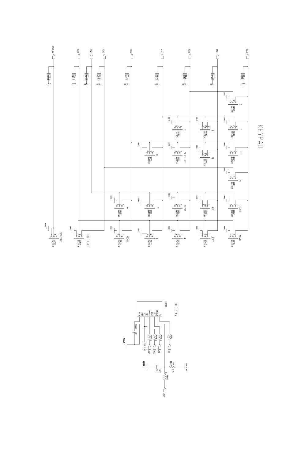
3.7.1 Display...................................................................................................................................................................... 19
3.7.2 Keypad...................................................................................................................................................................... 20
3.8 AUDIO INTERFACE .......................................................................................................................................................... 21
3.8.1 Speaker ..................................................................................................................................................................... 21
3.8.2 Microphone............................................................................................................................................................... 21
3.8.3 Audio Source Selection ............................................................................................................................................ 21
3.8.4 Headset ..................................................................................................................................................................... 22
3.8.5 Alert Speaker ............................................................................................................................................................ 23
3.9 DEVELOPER BOARD PERIPHERALS ............................................................................................................................ 23
3.9.1 SIM Card .................................................................................................................................................................. 23
3.9.2 Entertainment Mute .................................................................................................................................................. 24
3.9.3 LEDs Logic and Control........................................................................................................................................... 24
3.9.4 ADC Test Logic........................................................................................................................................................ 24
3.9.5 Ignition...................................................................................................................................................................... 25
3.9.6 Wakeup..................................................................................................................................................................... 25
3.9.7 AC Adapter Detection Circuit .................................................................................................................................. 25
3.10 ANTENNA CONFIGURATION....................................................................................................................................... 25
3.11 TEST POINTS ................................................................................................................................................................... 26
3.12 ELECTRICAL SPECIFICATIONS................................................................................................................................... 26
MECHANICAL DESCRIPTION
4.1 MECHANICAL REQUIREMENTS FOR MOUNTING THE G20 MODULE ................................................................. 27
SERVICE SUPPORT
5.1 WEB PAGES ....................................................................................................................................................................... 29
5.2 CUSTOMER ASSISTANCE............................................................................................................................................... 29
SCHEMATICS, PLACEMENT AND PARTS LIST
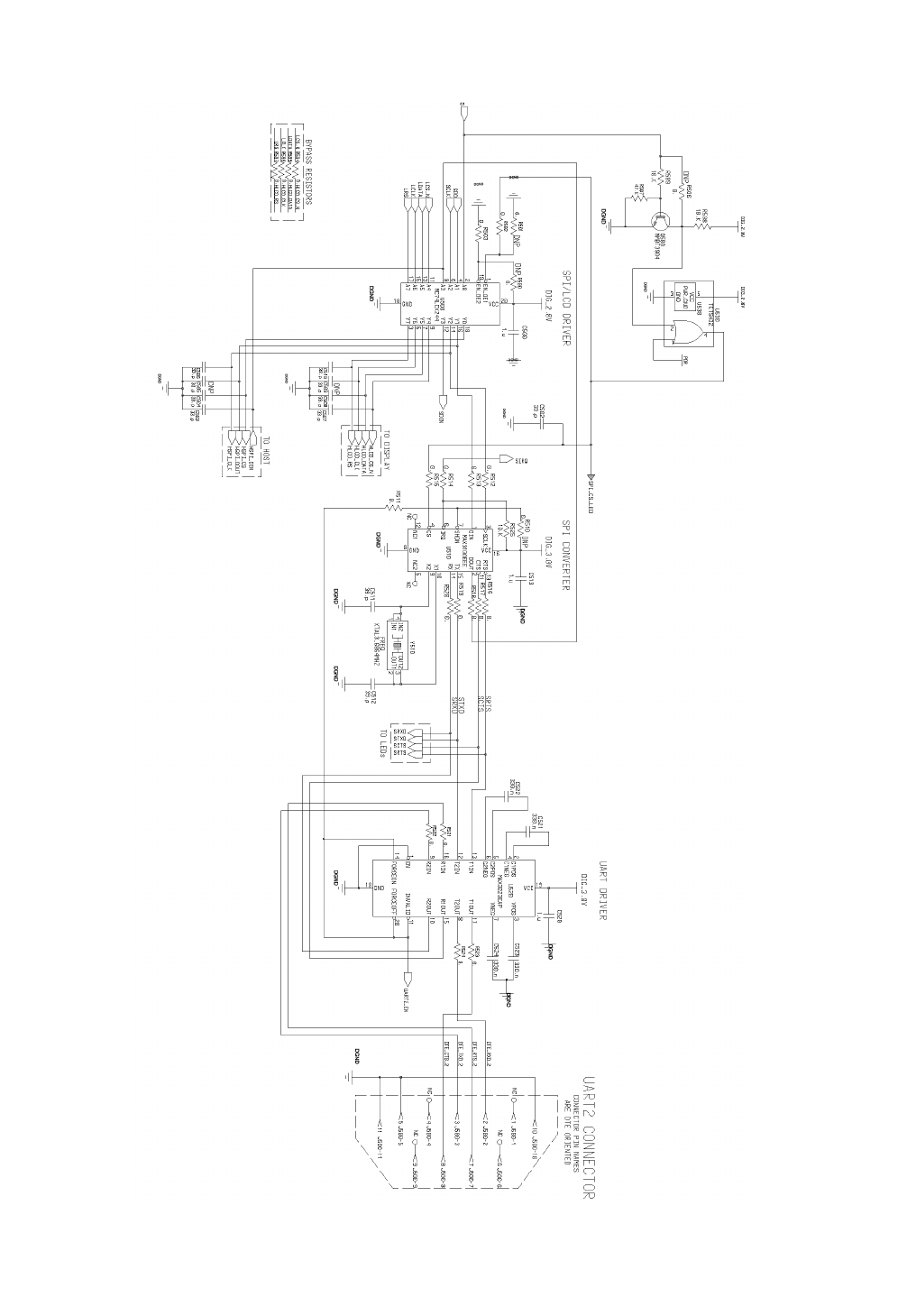
6.1 SCHEMATICS..................................................................................................................................................................... 31
6.2 DEVELOPERS BOARD PLACEMENT ............................................................................................................................ 41
6.3 DEVELOPER BOARD PARTS LIST................................................................................................................................. 43
ERRATA
7.1 SWITCH ASSIGNMENTS CORRECTION ....................................................................................................................... 49
INDEX
DRAFT 1 (31.3.03)

98-08901C67-O v
LIST OF FIGURES
Figure 1. Developer Board with Accessories ...............................................................................................................................5
Figure 2. Developer Board Components ......................................................................................................................................7
Figure 3. Mounting the g20 Module.............................................................................................................................................8
Figure 4. Attaching the RF Cable .................................................................................................................................................8
Figure 5. ADC Test Logic ..........................................................................................................................................................25
Figure 6. Mechanical Mounting Requirements ..........................................................................................................................27
Figure 7. .....................................................................................................................................................................................32
Figure 8. .....................................................................................................................................................................................33
Figure 9. .....................................................................................................................................................................................34
Figure 10. ...................................................................................................................................................................................35
Figure 11. ...................................................................................................................................................................................36
Figure 12. ...................................................................................................................................................................................37
Figure 13. ...................................................................................................................................................................................38
Figure 14. ...................................................................................................................................................................................39
Figure 15. ...................................................................................................................................................................................40
Figure 16. Developer Board Top Layout....................................................................................................................................41
Figure 17. Developer Board Bottom Layout ..............................................................................................................................42
Figure 18. S100 Options Switch Functions ................................................................................................................................49
DRAFT 1 (31.3.03)

vi 98-08901C67-O
LIST OF TABLES
Table 1. Terms and Abbreviations ............................................................................................................................................... 3
Table 2. RS232-1 Connector Pinout (J350) ............................................................................................................................... 10
Table 3. USB Connector Pinout (J3).......................................................................................................................................... 11
Table 4. USB Selection (P300 Jumper) ..................................................................................................................................... 11
Table 5. RS232-2 Connector Pinout (J500) ............................................................................................................................... 12
Table 6. Connectors.................................................................................................................................................................... 12
Table 7. g20 Connectors Pinout ................................................................................................................................................. 13
Table 8. J230 Connector Pinout ................................................................................................................................................. 16
Table 9. P600 Connector Pinout ................................................................................................................................................ 16
Table 10. Power Source (P202 Jumper)..................................................................................................................................... 16
Table 11. Switches and Jumpers ................................................................................................................................................ 17
Table 12. LED Indicators ........................................................................................................................................................... 18
Table 13. Display Connector Pinouts (DS800).......................................................................................................................... 19
Table 14. Keypad Functions...................................................................................................................................................... 20
Table 15. Speaker Connector Pinout (J430)............................................................................................................................... 21
Table 16. Microphone Connector Pinout (J460)........................................................................................................................ 21
Table 17. Audio Source (P420 Jumper) ..................................................................................................................................... 22
Table 18. Headset Connector Pinout (J440)............................................................................................................................... 22
Table 19. Alert Transducer Pinout (LS400)............................................................................................................................... 23
Table 20. SIM Connector Pinouts (J100)................................................................................................................................... 23
Table 21. SIM Detection Logic (P110 Jumper) ......................................................................................................................... 24
Table 22. Test Points.................................................................................................................................................................. 26
Table 23. Electrical Specifications............................................................................................................................................. 26
Table 24. Developer Board Parts List ........................................................................................................................................ 43
DRAFT 1 (31.3.03)

98-08901C64-O 1
1. PREFACE
1.1 SCOPE OF THIS MANUAL
This manual introduces the g20 Developer's Kit, and describes the technical details required by the data terminal equipment
(DTE) team to successfully integrate the Motorola g20 cellular engine into an original equipment manufacturer (OEM) wireless
host device. With the help of this manual, the DTE team can use the Developer's Kit to conduct a full series of test and evaluation
procedures on the g20, as well as perform application development.
We at Motorola want to make this guide as helpful as possible. Keep us informed of your comments and suggestions for
improvements.
You can reach us by email: GSM support-BSH015@email.mot.com.
1.2 WHO SHOULD USE THIS MANUAL
This manual is intended for all members of the DTE OEM integration team who will use the g20 Developer’s Kit, including
representatives from hardware, software and RF engineering disciplines.
1.3 DISCLAIMER
This guide provides advice and guidelines to OEM teams. Responsibility regarding how the information is used lies entirely
with the OEM. Statements indicating support provided by, or offered by, Motorola are subject to change at any time.
Motorola reserves the right to make any changes to this manual.
1.4 REGULATORY REQUIREMENTS
The Federal Communications Commission (FCC) requires application for certification of digital devices in accordance with
CFR Title 47, Part 2 and Part 15. This includes Electromagnetic Energy Exposure (EME) testing. As the g20 modem is not a
standalone transceiver but is an integrated module, the g20 cannot be tested by itself for EME certification. It is, however, the
integrator’s responsibility to have the completed device tested for EME certification.
1.5 REGULATORY STATEMENT
The following safety precautions must be observed during all phases of the operation, usage, service or repair of any cellular
terminal or mobile incorporating the g20 module. Manufacturers of the cellular terminal are advised to convey the following
safety information to users and operating personnel, and to incorporate these guidelines into all manuals supplied with the prod-
uct. Failure to comply with these precautions violates safety standards of design, manufacture and intended use of the product.
Motorola assumes no liability for customer failure to comply with these precautions.
1. The g20 must be operated at the voltages described in the technical documentation.
2. The g20 must not be mechanically nor electrically changed. Use of connectors should follow the guidance of the technical
documentation.
3. The g20 is designed the meet the EMC requirements of ETS 300 342.
DRAFT 1 (31.3.03)

Preface
2 98-08901C64-O
4. When integrating the g20 into a system, Motorola recommends testing the system to ETS300342-1.
5. The g20 meets the safety requirements of EN60950.
6. Systems using the g20 are subject to mandatory EMC testing under directive 89/336/EEC (see item 3 above). Other
directives, such as the LVD directive 73/23/EE, may also apply to a system using the g20 module.
1.6 SAFETY
1.6.1 User Operation
Do not operate your telephone when a person is within eight inches (20 centimeters) of the antenna. A person or object within
eight inches (20 centimeters) of the antenna could impair call quality and may cause the phone to operate at a higher power level
than necessary, as well as expose that person to RF energy in excess of that established by the FCC RF Exposure Guidelines.
IMPORTANT: The telephone must be installed in a manner that provides a minimum separation distance of 20 cm or more
between the antenna and persons in order to satisfy FCC RF exposure requirements for mobile transmitting devices.
IMPORTANT: To comply with the FCC RF exposure limits and satisfy the categorical exclusion requirements for mobile
transmitters, the requirements described in the section that follows must be met.
1.6.2 Antenna Installation
• A minimum separation distance of 20 cm must be maintained between the antenna and all persons.
• The effective radiated power of the transmitter must be less than 1.5 Watts ERP (2.45 Watts or 33.9 dBm EIRP). This requires
that the combination of antenna gain and feed line loss does not exceed 11 dBi.
1.7 APPLICABLE DOCUMENTS
g20 Cellular Engine Module Description: 9808901C66-O
g20 AT Commands: 9808901C68-O
1.8 HOW THIS MANUAL IS ORGANIZED
This manual contains the following chapters:
•Chapter 1 contains this Preface.
•Chapter 2 introduces the g20 Developer’s Kit and provides important safety instructions.
•Chapter 3 describes the Developer Board and its components in detail, including connectors, jumpers, DIP switches and
LED indicators. It also includes a set of Quick Start procedures for first-time use.
•Chapter 4 provides a mechanical description of the Developer Board.
•Chapter 5 provides contact information for Motorola Service Support and Customer Assistance.
•Chapter 6 includes schematic diagrams of the g20 Developer’s Kit as well as a complete parts list.
• Errata provides a correction to the Developer Board.
DRAFT 1 (31.3.03)

98-08901C64-O 3
2. INTRODUCTION
2.1 GENERAL DESCRIPTION
The g20 Developer’s Kit is intended for evaluating the g20 module, as well as for developing and testing software applications
for it.
2.2 TERMS AND ABBREVIATIONS
This section provides definitions for terms and acronyms used in this document.
2.3 SAFETY PRECAUTIONS
Most Developer Board circuits are not shielded. Be sure to take appropriate precautionary measures in order to avoid ESD while
handling the kit. ESD can damage the Developer Board and/or the g20 module attached to it.
Table 1. Terms and Abbreviations
Acronym/Term Definition/Description
ADC Analog to Digital Converter
CMOS Complementary Metal Oxide Semiconductor
CODEC Coder-Decoder
DTE Data Terminal Equipment (such as terminals, PCs and so on)
GPRS General Packet Radio Service
GSM Global System for Mobile Communications
IGN WHAT DOES THIS STAND FOR?
IRQ Interrupt Request
LED Light-Emitting Diode
MMCX Multimedia Communications Exchange
PCM Pulse Code Modulation
RF Radio Frequency
SIM Subscriber Identity Module
SPI Serial Peripheral Interface
UART Universal Asynchronous Receiver Transmitter
USB Universal Serial Bus
UUT Unit Under Test
DRAFT 1 (31.3.03)

Introduction
4 98-08901C64-O
DRAFT 1 (31.3.03)

98-08901C64-O 5
3. DEVELOPER BOARD AND
INTERFACES DESCRIPTION
3.1 GENERAL
The g20 Developer Board is designed to support the hardware and software development and validation of the g20 GSM/GPRS
data module. The Developer Board provides a peripheral platform to operate the g20 as a standalone product, and to easily
access the g20 interface connector signals.
The Developer Board has the following functions:
• Serves as a mounting platform for the g20 module
• Supplies the g20 module with supply voltage
• Provides standard communication interfaces (USB and RS232)
Kit Number: FTN8121A
Board Number: 8487653U01
Revision: P3
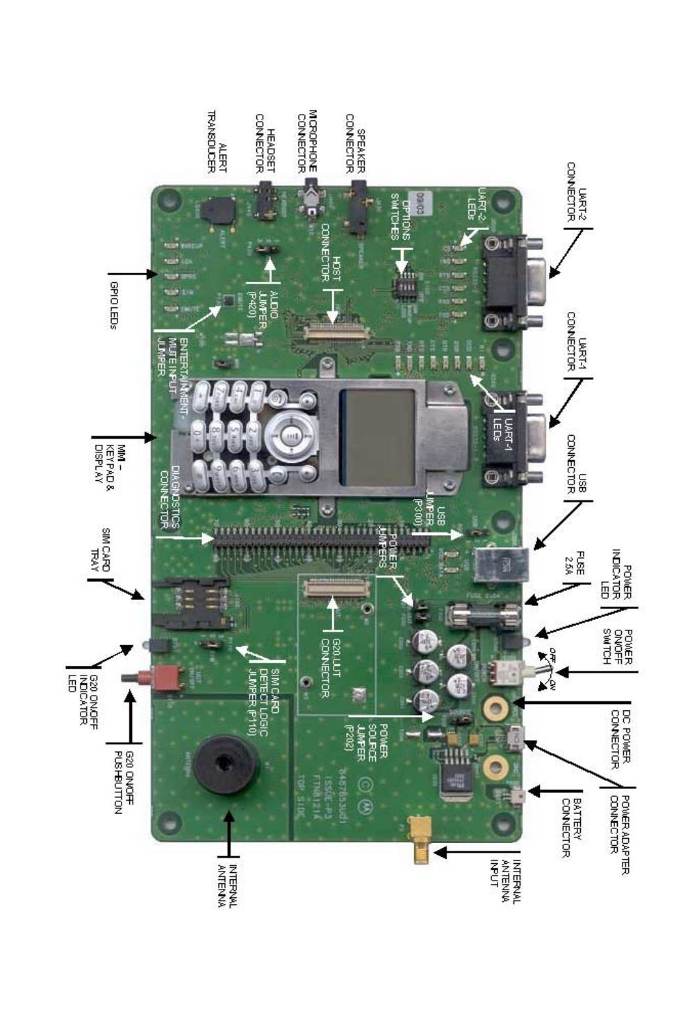
Figure 1 shows the Developer Board and some of its accessories with the g20 module attached to it: PLEASE PROVIDE
GRAPHIC.
Figure 1. Developer Board with Accessories
DRAFT 1 (31.3.03)

Developer Board and Interfaces Description
6 98-08901C64-O
3.1.1 Developer Board Features
The Developer Board provides the following features to facilitate software and hardware development:
• Output of all g20 connector signals to a large header connector for debugging
• Host-systems connector
• AC, battery and DC power supplies for board operation
• LED indicators for critical signals
• Display and keypad for phone operation
• USB and RS232 serial interfaces
• Secondary RS232 interface using the SPI bus
• Digital audio interface
• Analog audio interface for speaker, alert speaker, microphone and headset
• SIM card connector
• Switches and jumpers for controlling board operation
DRAFT 1 (31.3.03)
98-08901C64-O 7
Developer Board and Interfaces Description
3.1.2 Developer Board Connectivity
Figure 2 shows the Developer Board and its components:
Figure 2. Developer Board Components
DRAFT 1 (31.3.03)

Developer Board and Interfaces Description
8 98-08901C64-O
3.1.3 Quick Start
This section describes a series of Quick Start procedures for first-time use of the Developer Board.
3.1.3.1 g20 Connection
Open the top cover of the Developer Board and insert the g20 in its designated position. The g20 should connect to the 70-pin
connector, labeled UUT (P1), and its holes should be aligned with the spacers on the Developer Board.
Fasten the g20 to the Developer Board spacers using two M2x0.4x6 mm screws provided with the kit. PLEASE PROVIDE
GRAPHIC.
Figure 3. Mounting the g20 Module
3.1.3.2 Antenna Connection
Connect the on-board antenna cable to the g20 antenna connector. Connect the RF Out output to the Internal antenna input using
the supplied cable. PLEASE PROVIDE GRAPHIC.
Figure 4. Attaching the RF Cable
Note
While working, you can keep the box closed.
DRAFT 1 (31.3.03)

98-08901C64-O 9
Developer Board and Interfaces Description
3.1.3.3 Power Connection
The Developer Board can be powered using either a wall-mounted adapter, a DC power supply or a battery cell.
Connect the adapter to the wall outlet and to the Developer Board adapter connector (J230) labeled Adapter.
3.1.3.4 Serial Connection
The USB and RS232 serial interfaces are available for PC communications. If a PC connection is required, connect either an
RS232 cable with a male D-Type connector to the labeled UART1 connector, or a USB cable with a B-Type connector to the
labeled USB connector.
3.1.3.5 Audio Connection
The Developer Board has several available audio configurations:
• Hands-free audio using the speaker and microphone
• Digital PCM audio
• Personal headset audio
Connect the supplied headset to the headset connector (J440) labeled Headset.
3.1.3.6 SIM Card Connection
Insert a SIM card into the SIM tray (J100).
3.1.3.7 Default Switches and Jumper Settings
The Developer Board jumpers and switches are initially configured to comply with this Quick Start operation mode. If different
settings are necessary, refer to the relevant section for details about the required switch or jumper settings.
3.1.3.8 Operating the g20
After completing the initial setup, turn on the Developer Board power by switching the power switch (S200) to its on position,
and turn on the g20 by depressing the on/off switch (S110) or by depressing the on/off button on the keypad.
Note
Only the adapter option is covered in this section. See “Power Connections” on page 15., when using other power
methods.
Note
The power source selection jumper, labeled Source, must be in the correct position for adapter operation (pins 1-2
shorted).
Note
When using a USB interface, be sure the USB jumper (P300) position reflects the g20 version being used. See
“USB” on page 11..
Note
Only the headset audio option is covered in this section. See “Audio Interface” on page 21. when using other audio
options.
Note
When using a SIM card, be sure the SIM jumper (P110) position reflects the g20 version being used. See “SIM
Card” on page 23. for more details.
DRAFT 1 (31.3.03)
Developer Board and Interfaces Description
10 98-08901C64-O
3.2 COMMUNICATIONS INTERFACES
The g20 Developer Board includes three different serial interfaces:
•RS232
•USB
• SPI
The RS232 and USB ports are multiplexed within the g20, and therefore cannot be operated simultaneously. Their default
connection is RS232. The SPI interface is used for debugging.
Each of these serial interfaces is described in the sections that follow.
3.2.1 RS232
The RS232 serial port is the primary interface to the g20 UUT via the J350 connector. This port is denoted by the RS232-1
marking beside the 9-pin, D-type connector.
The UUT RS232 signals are active-low CMOS-level signals (0-2.7 V), which are converted by the Developer Board to standard
RS232 levels for PC communications.
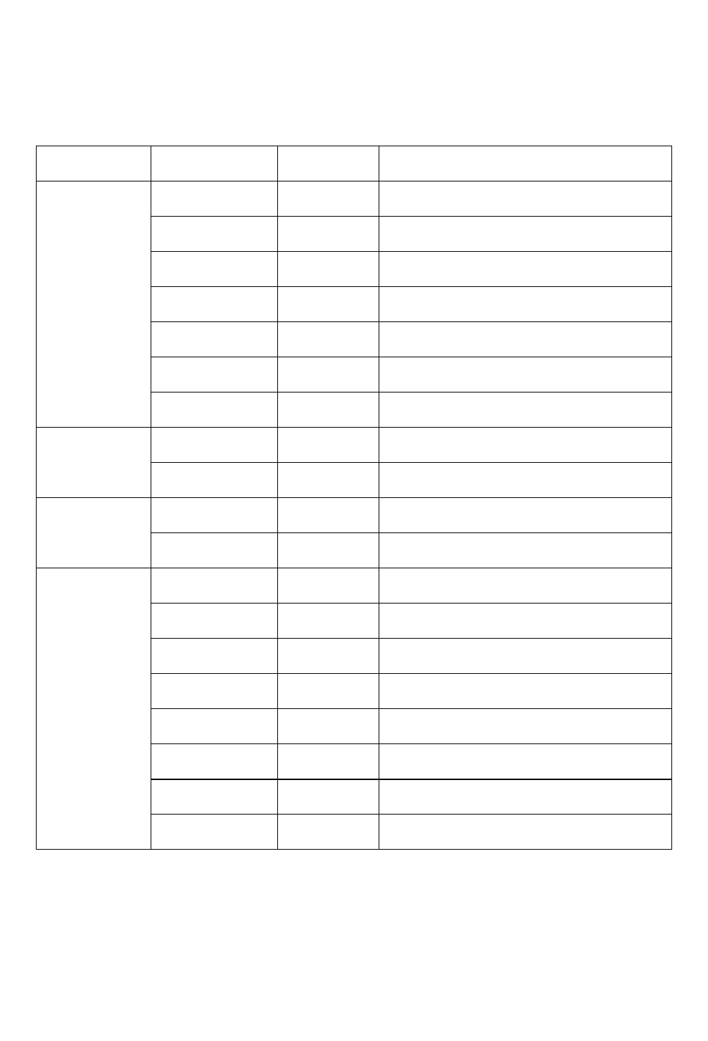
Table 2. RS232-1 Connector Pinout (J350)
Pin # Description DTE I/O
1 DCD In
2RXD In
3TXD Out
4DTR Out
5 Ground
6DSR In
7RTS Out
8CTS In
9RI In
Note
The RS232 connector pin names are DTE-oriented.
DRAFT 1 (31.3.03)
98-08901C64-O 11
Developer Board and Interfaces Description
3.2.2 USB
The USB interface operates according to the g20 UUT configuration. The Developer Board has a complete USB transceiver
circuit to support USB communications for g20 units that do not include a USB driver of their own. The Developer Board USB
interface can be overridden manually when using a g20 unit that does include its own USB driver interface.
The USB jumper (P300) located next to the USB connector selects between the Developer Board USB interface and the UUT
USB interface. By changing the jumper position, the USB_VBUS signal is diverted to the selected driver (in the g20 or on the
Developer Board) and operates it.
3.2.3 SPI
The Developer Board includes a secondary 4-wire RS232 interface, which is connected to the g20 internal SPI bus through the
J500 connector. This interface is used to debug applications. This port is denoted by the RS232-2 label next to the 9-pin D-type
connector.
Table 3. USB Connector Pinout (J3)
Pin # Description
1VCC
2D-
3D+
4Ground
Table 4. USB Selection (P300 Jumper)
P300
Jumper
Position
Selected Mode USB Source
12 3
•• g20 g20 driver
••EVB (Developer Board) EVB driver
USB disconnected
DRAFT 1 (31.3.03)
Developer Board and Interfaces Description
12 98-08901C64-O
On the Developer Board, the g20 SPI interface is converted to standard RS232 signals for PC communications. The conversion
process uses the RS232 interface as a second slave on the internal g20 SPI bus, and communicates with it as such. SPI read and
write operations are performed normally, using the CS and IRQ signals provided by the conversion circuit. The IRQ signal is
connected to a g20 IRQ pin.
3.3 CONNECTORS DESCRIPTION
All the Developer Board connectors are marked by their reference number and by a pin-1 indicator. Table 6 describes the avail-
able connectors on the Developer Board.
Note
The RS232 connector pin names are DTE-oriented.
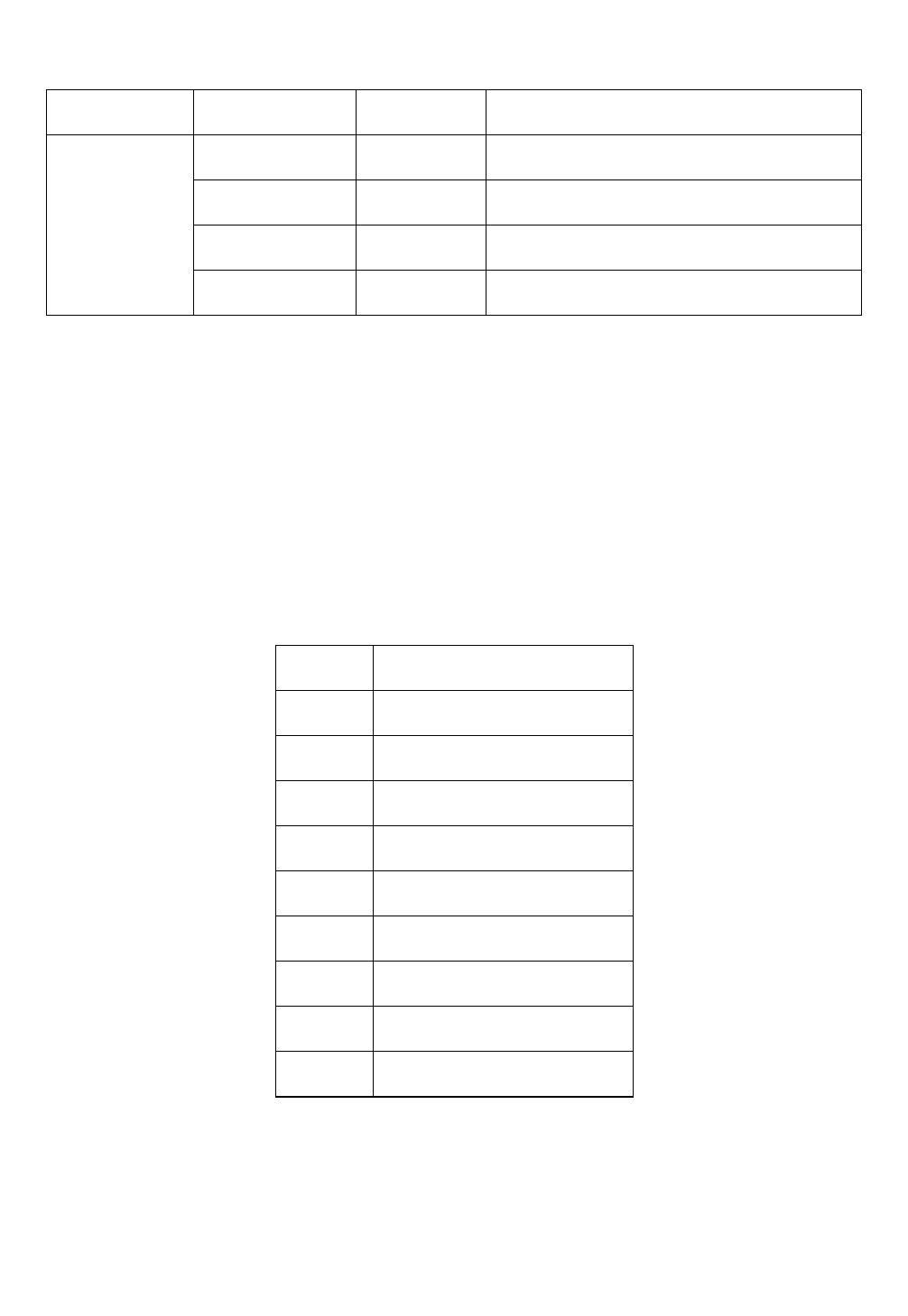
Table 5. RS232-2 Connector Pinout (J500)
Pin # Description DTE I/O
1Unused
2RXD In
3TXD Out
4Unused
5 Ground
6Unused
7RTS Out
8CTS In
9Unused
Table 6. Connectors
Reference Connector Description
P1 g20 UUT g20 UUT (unit under test) connector
J1 Host Emulates the g20 connector for host systems
P100 Diagnostics Debug header connector (70-pin)
J300 USB USB B-type connector
J350 RS232-1 Primary RS232 to PC
J500 RS232-2 Secondary RS232 for debugging (SPI)
DRAFT 1 (31.3.03)
98-08901C64-O 13
Developer Board and Interfaces Description
3.3.1 UUT Interface Connector
Table 7 lists the pin names and functions available for g20 interface connectors. All pin numbers and functions are identical for
the P1, J1 and P100 connectors on the Developer Board.
J430 Speaker Hands-free system speaker jack
J460 Microphone Hands-free system microphone jack
J440 Headset Headset jack
J201 VCC Developer Board DC power supply
J200 GND Developer Board common ground
P600 Battery Battery connector
J230 AC adapter/charger Wall-mount adapter connector (CE bus
compatible)
J100 SIM card SIM card socket with detection
P2 Antenna connector SMA connector for g20 antenna
M1 RF Antenna RF antenna
DS800 Display Display pads
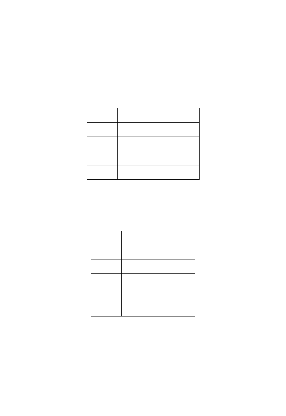
Table 7. g20 Connectors Pinout
Pin # Pin Name Pin # Pin Name
1 GND 2 GND
3 GND 4 GND
5 VCC 6 VCC
7 VCC 8 VCC
9 RTS_N 10 USB_DET
11 RXD_N 12 Not connected
13 DSR_N 14 Not connected
15 CTS_N 16 WAKEUP_IN_N
Table 6. Connectors (Continued)
Reference Connector Description
DRAFT 1 (31.3.03)

Developer Board and Interfaces Description
14 98-08901C64-O
17 DCD_N 18 PCM_DIN
19 DTR_N 20 PCM_DOUT
21 TXD_N 22 PCM_CLK
23 RI_N 24 PCM_FS
25 RESET_N 26 WAKEUP_OUT_N
27 BL_SINK 28 KBC1_N
29 CHRG_DIS 30 KBC0_N
31 CHRG_SW 32 KBR0_N
33 CHRG_STATE 34 KBR1_N
35 CHRG_DET_N 36 KBR2_N
37 ENT_MUTE 38 KBR3_N
39 TX_EN_N 40 KBR4_N
41 ANT_DET 42 KBR5_N
43 VIB_OUT 44 SIM_RST_N
45 CHRG_TYP 46 SIM_CLK
47 THERM 48 SIM_VCC
49 GPRS_DET_N 50 SIM_PD
51 IGN 52 SIM_DIO
53 ON_OFF_N 54 LCD_CS
55 HDST_INT_N 56 LCD_DATA
57 HDST_MIC 58 LCD_CLK
59 MIC_GND 60 LCD_RS
61 MIC 62 SPI_IRQ_N
63 ALRT_N 64 SPI_DIN
Table 7. g20 Connectors Pinout (Continued)
Pin # Pin Name Pin # Pin Name
DRAFT 1 (31.3.03)
98-08901C64-O 15
Developer Board and Interfaces Description
3.4 POWER CONNECTIONS
Developer Board power can be supplied from a DC power source, an AC power adapter or a battery. The same power source is
used for the UUT and the board peripherals.
The Developer Board includes three jumpers for controlling the power supply:
•P202: AC adapter or battery power source selection
•P201: Connects/disconnects the Developer Board peripherals from the power supply
•P200: Connects/disconnects the g20 from the power supply
Each power supply option is described in the sections that follow.
3.4.1 DC Power Source Operation
When using a DC power supply, the power source is applied to connectors J201 (VCC) and J200 (Ground). The DC voltage
applied through this connection should not exceed the recommended operational limits of 3V-4.2V. In all cases, the DC source
input is protected from over voltage and reverse polarity, and includes a 2.5A protective fuse.
The supplied DC input connectors must be attached to the Developer Board in order to use the DC power source. The two
connectors should be screwed into their appropriate positions (J201, labeled VCC, and J200, labeled GND). Use the red connec-
tor for VCC and the black one for GND. Connect the DC power source to these connectors using banana plugs, alligator clamps
or wire.
65 ALRT_P 66 SPI_CLK
67 SPKR_N 68 SPI_DOUT
69 SPKR_P 70 SPI_CS
!
Caution
It is recommended to remove jumper P202 when using the DC power source. In any case, the DC power source
should not be used when other sources are connected.
Table 7. g20 Connectors Pinout (Continued)
Pin # Pin Name Pin # Pin Name
DRAFT 1 (31.3.03)
Developer Board and Interfaces Description
16 98-08901C64-O
3.4.2 AC Adapter Operation
When using an AC adapter, the adapter is connected to J230. The adapter supplies a constant 4.5 V, which is regulated to a
nominal 4.1 V on the Developer Board.
3.4.3 Battery Operation
The Developer Board supports a battery power supply. The battery used must be a 3.6V lithium-ion cell, corresponding to
Motorola part number 0189727L01.
When using a battery as the main power source, the AC adapter input operates as a battery charger, which connects to an
on-board battery charging circuit.
3.4.4 Power Source Selection
The Developer Board AC adapter and battery power inputs include a selection jumper (P202) that diverts either the regulated
AC adapter power or the battery power to the board.
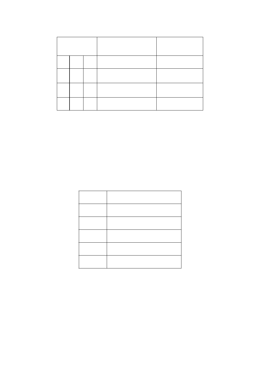
Table 8. J230 Connector Pinout
Pin # Pin Name
1GND
2 Detection circuit
3VCC
Table 9. P600 Connector Pinout
Pin # Pin Name
1VCC
2GND
Table 10. Power Source (P202 Jumper)
P202 Jumper
Position Selected Mode Power Source
12 3
•• Adapter AC Adapter
••Battery LiIon Battery
Adapter and battery disconnected DC power only
DRAFT 1 (31.3.03)
98-08901C64-O 17
Developer Board and Interfaces Description
3.5 SWITCHES AND JUMPERS
Table 11 describes the available switches and jumpers on the Developer Board.
Note
The DC power source input is independent of the other power inputs, and does not pass through this selection
jumper. Nevertheless, it is still recommended to disconnect the P202 jumper when using the DC source.
Table 11. Switches and Jumpers
Reference Switch/Jumper Description
S200 Board on/off Developer Board on/off switch
S110 g20 on/off g20 UUT on/off push button switch
S100 Options switch Four switches for Developer Board options
P420 Audio Analog/digital audio-selection jumper
P201 EVB Peripheral power input jumper
P200 UUT g20 UUT power input jumper
P202 Source Power source selection jumper
P110 SIM SIM card detect logic selection jumper
P300 USB USB driver source selection jumper
P130 EMUTE Entertainment mute connection point
DRAFT 1 (31.3.03)
Developer Board and Interfaces Description
18 98-08901C64-O
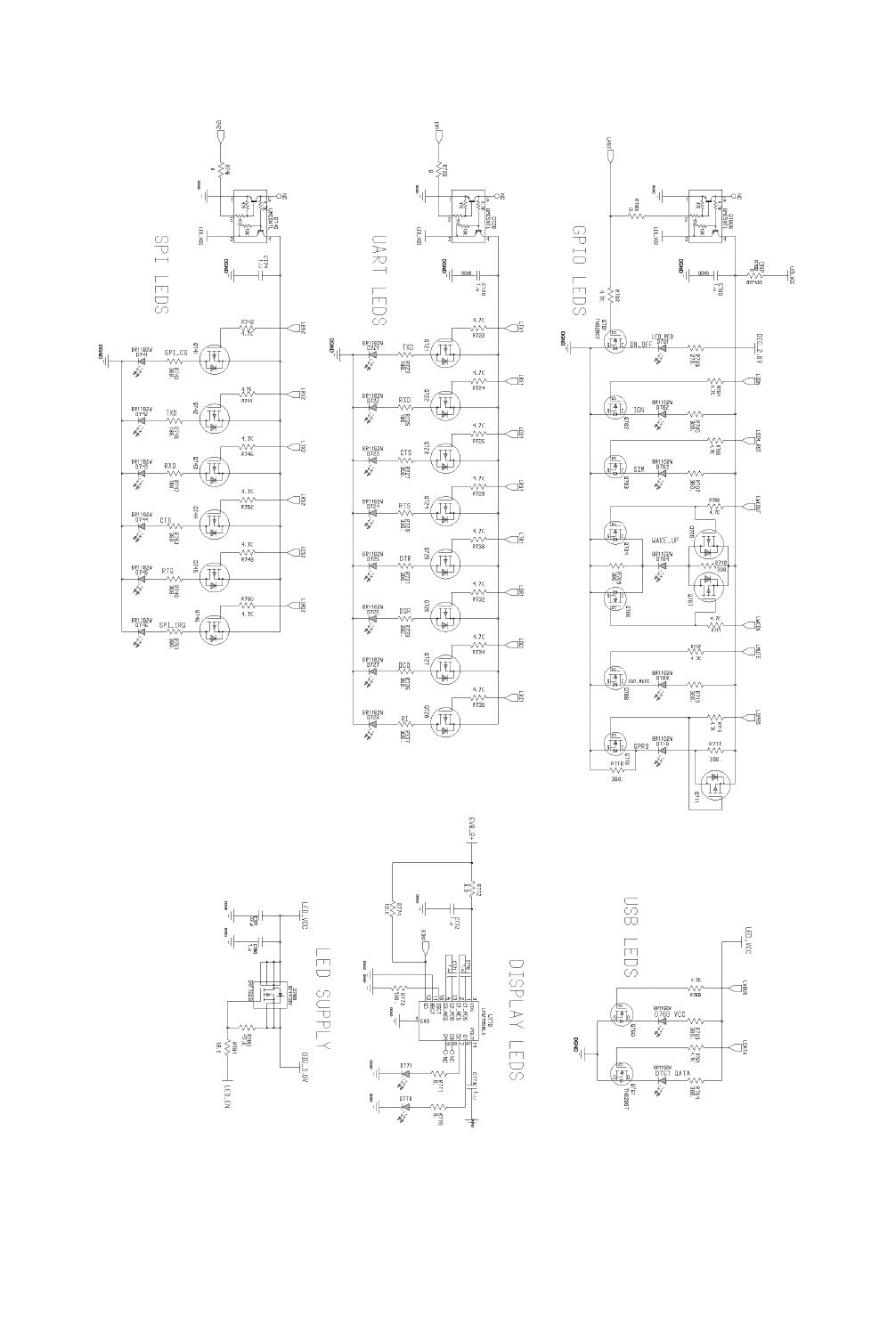
3.6 LED INDICATORS
Table 12 describes the LED indicators available on the Developer Board. Each LED is marked on the board by the function it
represents.
Table 12. LED Indicators
Group LED Reference Description
GPIO
WAKEUP D704 Wake-up in/out
IGN D702 Ignition input
GPRS D710 GPRS coverage indication
SIM D703 SIM card reset indication
UUT D701 g20 reset signal
PWR D200 Developer Board power indicator
EMUTE D708 Entertainment mute indicator
SPI
CS D741 SPI chip-select output
IRQ D745 SPI IRQ input
USB
VCC D760 USB VBUS
DATA D761 USB D+
RS232-1
RXD D722 DTE receive data
TXD D721 DTE transmit data
RTS D724 Request to send
CTS D723 Clear to send
DTR D725 Data terminal ready
DSR D726 Data set ready
DCD D727 Carrier detect
RI D728 Ring indicator
DRAFT 1 (31.3.03)
98-08901C64-O 19
Developer Board and Interfaces Description
3.7 MMI
The Developer Board includes a man-machine interface (MMI), complete with display and keypad. The signals from the display
and keypad are directly connected to the UUT interface.
3.7.1 Display
The grayscale display (DS800) is not a standalone component, and includes a complete assembly in which it is housed, along
with other necessary parts.
RS232-2
RXD D743 DTE receive data
TXD D742 DTE transmit data
CTS D744 Clear to send
RTS D745 Request to send
Table 13. Display Connector Pinouts (DS800)
Pin # Description
1Chip select
2Reset
3 Register select
4 Serial clock
5 Serial data
6 Supply
7 Supply
8Ground
9Vout
Table 12. LED Indicators (Continued)
Group LED Reference Description
DRAFT 1 (31.3.03)

Developer Board and Interfaces Description
20 98-08901C64-O
3.7.2 Keypad
Table 14 describes the Developer Board keypad layout.
Table 14. Keypad Functions
Pad Reference Function Alternate
S803 1 Punctuation
S802 2 ABC
S820 3 DEF
S801 4 GHI
S805 5 JKL
S804 6 MNO
S806 7 PQRS
S817 8 TUV
S811 9 WXYZ
S809 0 +
S810 Star (*)
S815 Pound (#)
S814 Send
S813 End On/Off
S819 Menu
S822 Right
S823 Left
S818 Up
S816 Down
S812 Soft Right
S808 Soft Left
DRAFT 1 (31.3.03)
98-08901C64-O 21
Developer Board and Interfaces Description
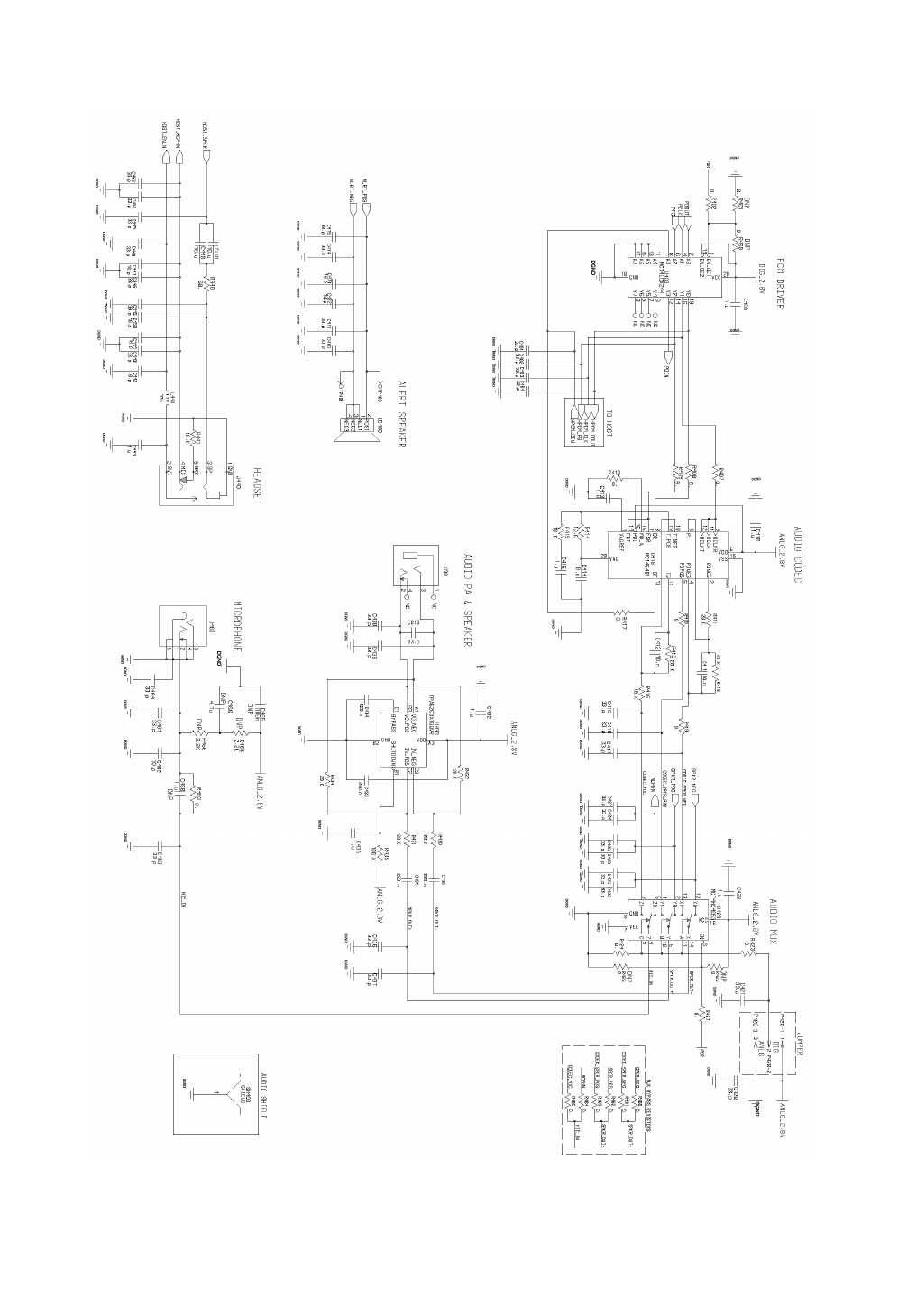
3.8 AUDIO INTERFACE
The Developer Board includes analog and digital audio interfaces. The audio interface contains a hands-free speaker and micro-
phone, a headset, and an alert speaker.
3.8.1 Speaker
The differential speaker interface is designed as a car-kit hands-free speaker. The Developer Board uses an audio amplifier to
amplify the speaker audio output to desired levels. The speaker connector (J430) is labeled SPEAKER. The speaker output is 8
ohms matched.
3.8.2 Microphone
The microphone interface is designed as a car-kit hands-free microphone. The microphone connector (J460) is labeled MIC.
3.8.3 Audio Source Selection
Microphone and speaker audio can be routed through two different sources: the g20 audio amplifiers or the g20 digital audio
interface. The Developer Board includes a CODEC that converts the g20 digital audio data to analog audio signals.
Table 15. Speaker Connector Pinout (J430)
Pin # Description
1 Not connected
2 Speaker positive output
3 Speaker negative output
4 Not connected
Table 16. Microphone Connector Pinout (J460)
Pin # Description
1Ground
2 Microphone audio-in
3Ground
4Ground
5Ground
DRAFT 1 (31.3.03)
Developer Board and Interfaces Description
22 98-08901C64-O
The P420 jumper selects the speaker and microphone source, as indicated in Table 17.
3.8.4 Headset
The headset interface is designed as a portable phone audio interface, and is similar to the headset interface. The headset connec-
tor (J440) includes a speaker, microphone and a detection signal. The speaker and microphone signals are directly connected to
the g20 audio signals.
The purpose of the detection circuit is to switch the g20 headset audio paths on and off, whenever a headset connection is
detected. Headset detection is made whenever a headset plug is inserted into the jack. This action disables the g20 microphone
and speaker, and routes the audio signals to the headset.
Table 17. Audio Source (P420 Jumper)
P420 Jumper
Position Selected Mode Audio Source
12 3
•• Digital audio CODEC audio I/O
••Analog audio G20 audio I/O
Audio disconnected
Table 18. Headset Connector Pinout (J440)
Pin # Description
1 Ground
2 Headset-detect switch
3 Speaker audio-out
4 Microphone audio-in
5 Ground
DRAFT 1 (31.3.03)
98-08901C64-O 23
Developer Board and Interfaces Description
3.8.5 Alert Speaker
The Developer Board includes an on-board transducer for alert audio sounds (LS400), which is labeled ALERT. The transducer
is connected directly to the g20 differential alert outputs. The alert transducer is similar to the alert speaker, which sounds the
g20 MIDI signals.
3.9 DEVELOPER BOARD PERIPHERALS
This section describes the connectors for peripheral devices that can be used with the Developer Board.
3.9.1 SIM Card
The SIM card connector (J100) is external to the UUT, but is connected directly to it, similar to an internal SIM. The UUT can
accept 1.8V and 3V SIM cards.
Table 19. Alert Transducer Pinout (LS400)
Pin # Description
1 Alert audio inverted output
2 Alert audio positive output
3 Alert audio inverted output
4 Alert audio inverted output
Table 20. SIM Connector Pinouts (J100)
Pin Description
1Ground
2 Presence detect
3Clock
4Reset
5VCC
6 Serial data I/O
7 VPP
8Ground
DRAFT 1 (31.3.03)
Developer Board and Interfaces Description
24 98-08901C64-O
The SIM card supports both active-high and active-low detection configurations. Jumper P110 is used to select between these
configurations.
3.9.2 Entertainment Mute
The Developer Board includes an entertainment-mute logic circuit that is responsible for muting a car radio whenever the phone
is in use (for example, incoming calls, dialing, and so on).
The entertainment-mute logic circuit includes an ENABLE input that is both a g20 signal and an open-collector MUTE output.
This circuit is connected to jumper P130 for host systems.
3.9.3 LEDs Logic and Control
The Developer Board includes LED indicators for critical signals. A 3.0V regulator powers the LEDs, and an on/off switch
controls their operation. The switch is located in the S100 switch array, and is labeled LED. Turning the switch on and off
enables or disables all LED activity, respectively.
The Developer Board power LED and the g20 on/off LED are always active and cannot be disabled.
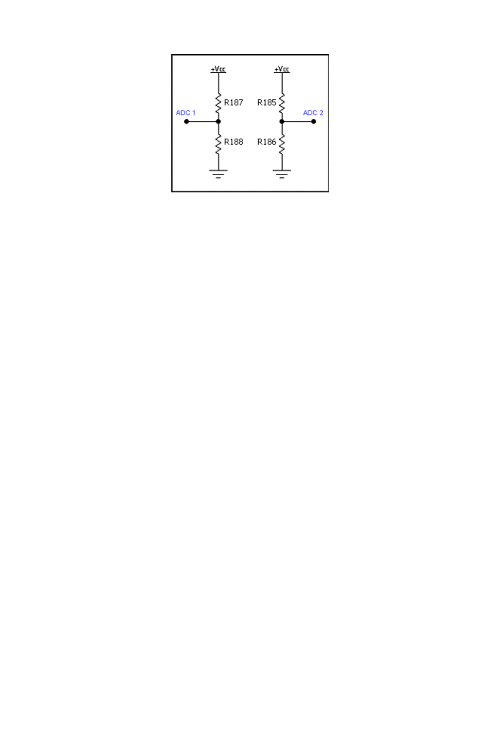
3.9.4 ADC Test Logic
The g20 has two ADC pins. The g20 charger and temperature monitor currently occupy these pins. The Developer Board
includes optional resistors for ADC testing. These resistors, two for each ADC signal, can be used to set a specific voltage across
the ADC signal.
Table 21. SIM Detection Logic (P110 Jumper)
P110 Jumper
Position Selected Mode
12 3
•• Active-low
••Active-high
Not active
Note
The entertainment-mute operation is not currently supported by the g20.
DRAFT 1 (31.3.03)
98-08901C64-O 25
Developer Board and Interfaces Description
The G20 has a 47K-ohm internal pull-up resistor at each ADC input, as shown in Figure 5.
Figure 5. ADC Test Logic
3.9.5 Ignition
The Developer Board contains an on/off switch that is connected to the g20 UUT ignition circuit. The switch is located in the
S100 switch array, and is labeled IGN. Turning the switch on applies the UUT supply on the Ignition input pin.
3.9.6 Wakeup
The Developer Board includes a wakeup switch that toggles the g20 WAKEUP_IN_N signal. The switch is located in the S100
switch array, and is labeled WAKEUP.
3.9.7 AC Adapter Detection Circuit
The g20 charger module includes a detection logic circuit for detecting charger presence and type. The detection circuit is inter-
nal to the g20 module. However, the Developer Board does contain the necessary routing from the g20 UUT to the AC adapter
connector.
Two g20 signals are used for this detection:
•AD1: ADC signal for charger type detection
•CHRG_SW: Charger rate control
These detection signals are present to provide compatibility with the phone. They may be removed in future versions.
3.10 ANTENNA CONFIGURATION
An antenna (internal or external) must be connected to the Developer Board for adequate GSM reception. You can connect the
g20 to either the on-board internal antenna or to an external antenna. Two RF connectors on the Developer Board, labeled INT
ANT and EXT ANT, are used for this purpose. The EXT ANT connector has an internal extension cable with MMCX termina-
tion, which must be connected to the g20 RF connector. The INT ANT connector is an on-board connection to the Developer
Board internal antenna.
When using the internal antenna option, the additional RF cable supplied in the Developer’s Kit must be connected between the
EXT ANT and INT ANT connectors. When using the external antenna option, an external antenna or antenna application must
be connected to the EXT OUT connector. (The connection cable is not included.)
DRAFT 1 (31.3.03)
Developer Board and Interfaces Description
26 98-08901C64-O
3.11 TEST POINTS
Table 22 describes the available test points on the Developer Board.
3.12 ELECTRICAL SPECIFICATIONS
Table 23 describes the electrical specifications OF the Developer Board.
* Depends on the active peripherals (LEDs, UART, USB, and so on) in use.
Table 22. Test Points
Reference Function
TP400 Alert speaker positive signal
TP401 Alert speaker inverted signal
Table 23. Electrical Specifications
Parameter Min Typ Max Units
DC power supply 3.0 3.6 4.2 V
Adapter power supply 4.4 4.6 12 V
Battery power supply 3.0 3.6 4.2 V
Off current --- 36 46 uA
On current 8.1 8.33 8.45 mA
Active current peripherals off 12.7 13 --- mA
Active current peripherals on*13.1 --- 190 mA
DRAFT 1 (31.3.03)
98-08901C64-O 27
4. MECHANICAL DESCRIPTION
4.1 MECHANICAL REQUIREMENTS FOR MOUNTING THE G20 MODULE
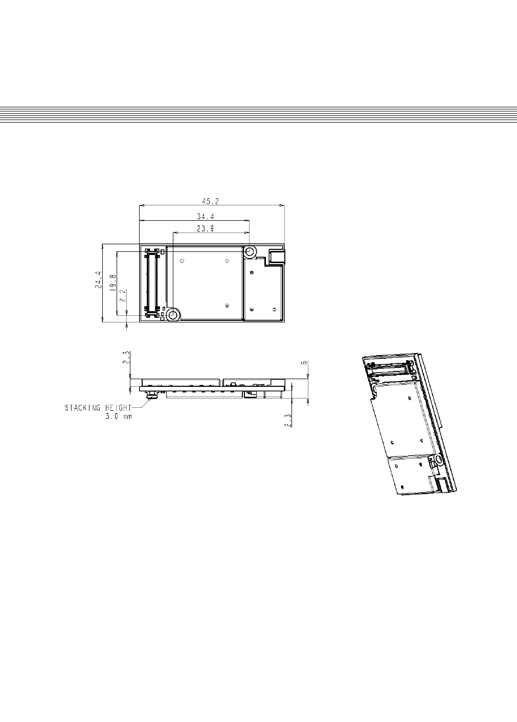
The size of the g20 module is 45.2 x 24.4 x 6 mm. Two 2.4 mmØ holes are provided to accommodate M2 screws or #1-64 UNC
2A machine screws. Torque to 2 inches per pound. Refer to Figure 6 below for mounting requirements:
Figure 6. Mechanical Mounting Requirements
DRAFT 1 (31.3.03)

Mechanical Description
28 98-08901C64-O
DRAFT 1 (31.3.03)

98-08901C64-O 29
5. SERVICE SUPPORT
5.1 WEB PAGES
PLEASE PROVIDE DETAILS FOR THIS SECTION.
5.2 CUSTOMER ASSISTANCE
For customer assistance, contact us as directed below:
Helpdesk email: n2cshd@motorola.com
Helpdesk telephone: +972-3-568-4040
DRAFT 1 (31.3.03)

Service Support
30 98-08901C64-O
DRAFT 1 (31.3.03)

98-08901C64-O 31
6. SCHEMATICS, PLACEMENT AND
PARTS LIST
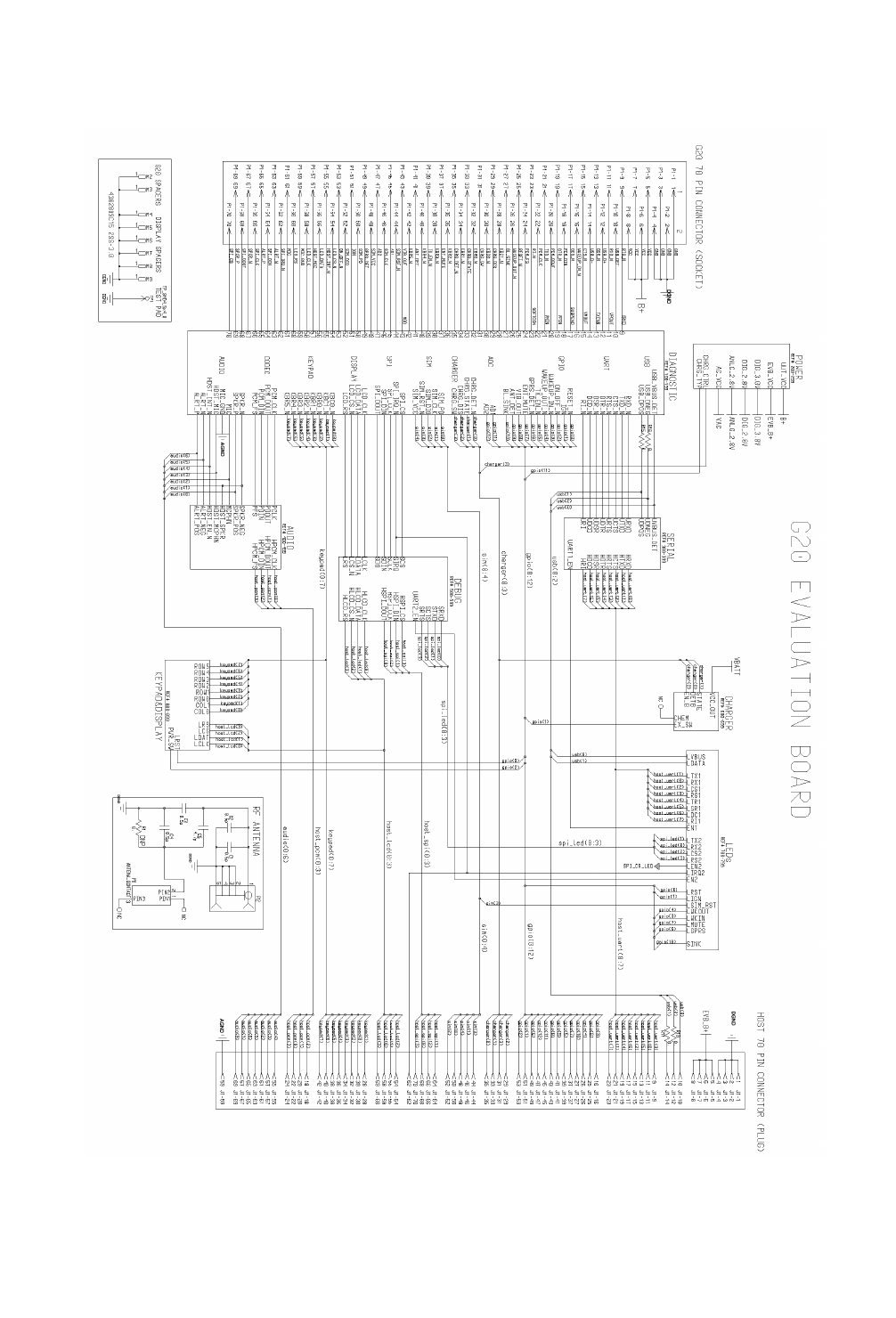
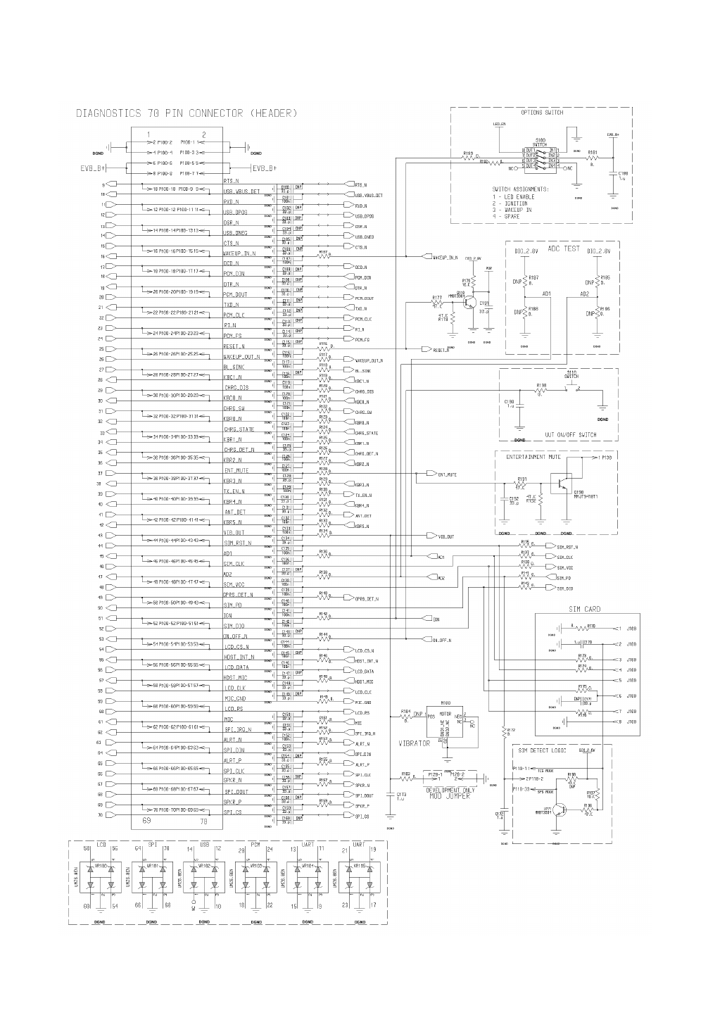
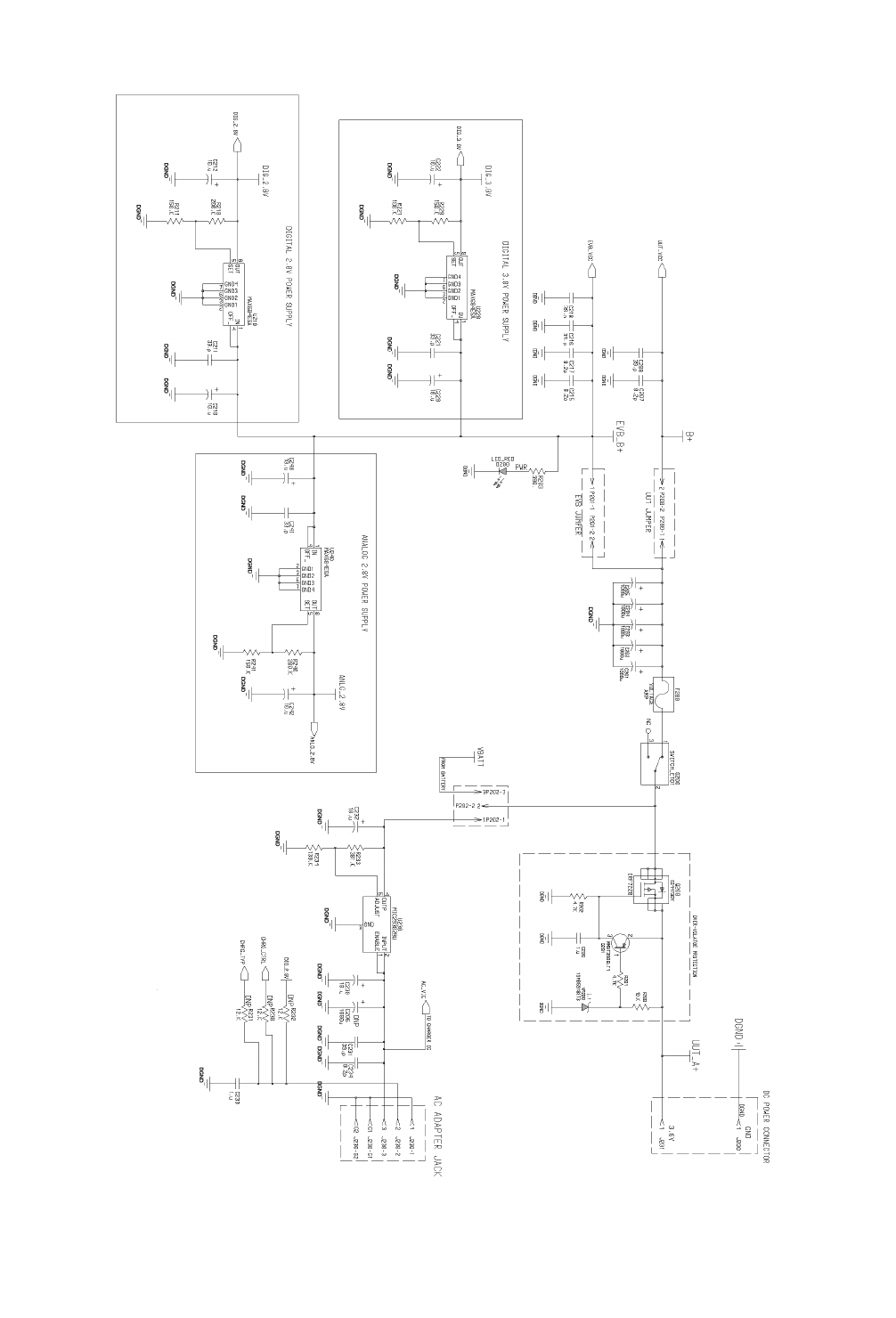
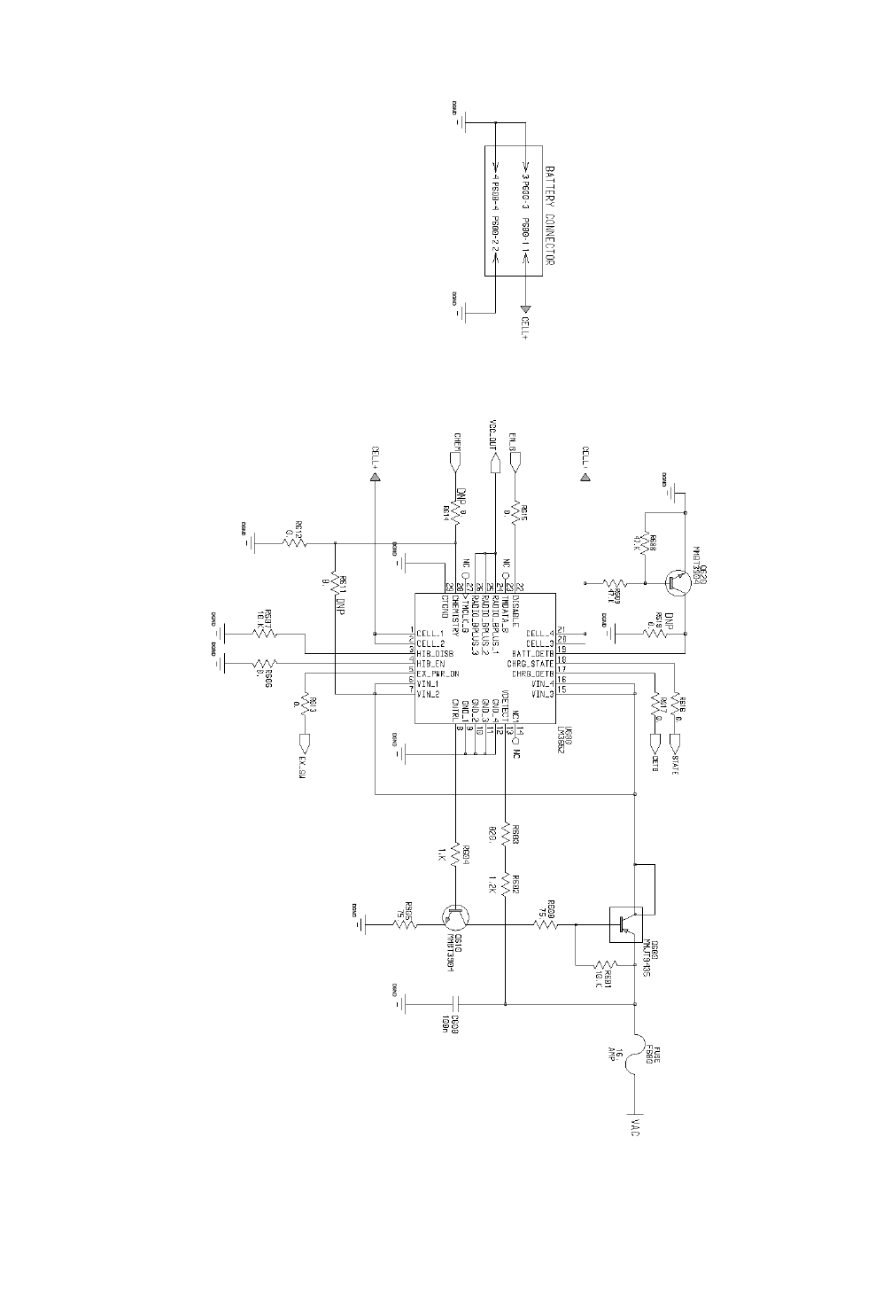
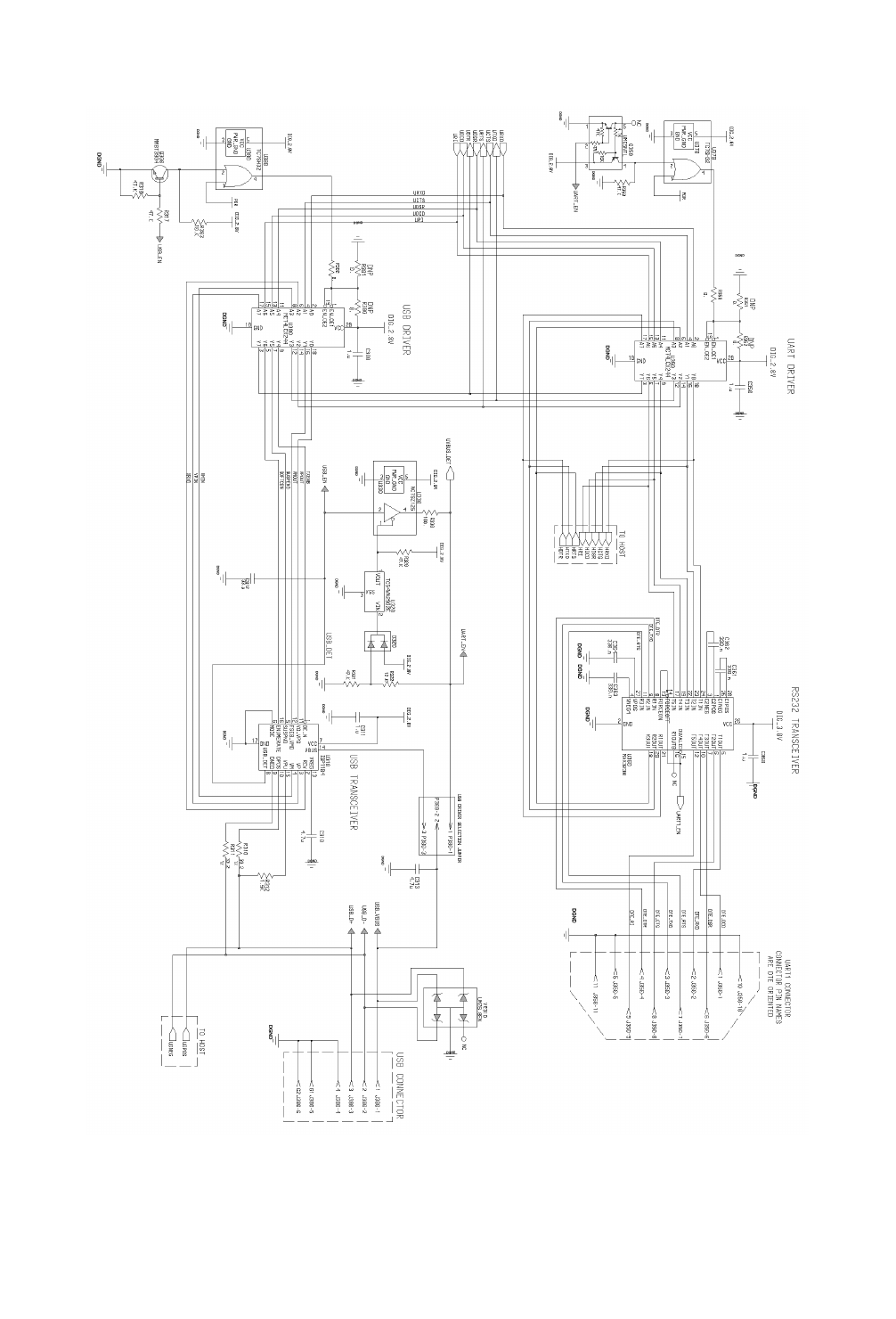
6.1 SCHEMATICS
This section presents the schematics for the g20 Developer Board.
PLEASE PROVIDE INFORMATION FOR FIGURE CAPTIONS.
DRAFT 1 (31.3.03)
Schematics, Placement and Parts List
32 98-08901C64-O
Figure 7.
DRAFT 1 (31.3.03)
98-08901C64-O 33
Schematics, Placement and Parts List
Figure 8.
DRAFT 1 (31.3.03)
Schematics, Placement and Parts List
34 98-08901C64-O
Figure 9.
DRAFT 1 (31.3.03)
98-08901C64-O 35
Schematics, Placement and Parts List
Figure 10.
DRAFT 1 (31.3.03)
Schematics, Placement and Parts List
36 98-08901C64-O
Figure 11.
DRAFT 1 (31.3.03)
98-08901C64-O 37
Schematics, Placement and Parts List
Figure 12.
DRAFT 1 (31.3.03)
Schematics, Placement and Parts List
38 98-08901C64-O
Figure 13.
DRAFT 1 (31.3.03)
98-08901C64-O 39
Schematics, Placement and Parts List
Figure 14.
DRAFT 1 (31.3.03)
Schematics, Placement and Parts List
40 98-08901C64-O
Figure 15.
DRAFT 1 (31.3.03)
98-08901C64-O 41
Schematics, Placement and Parts List
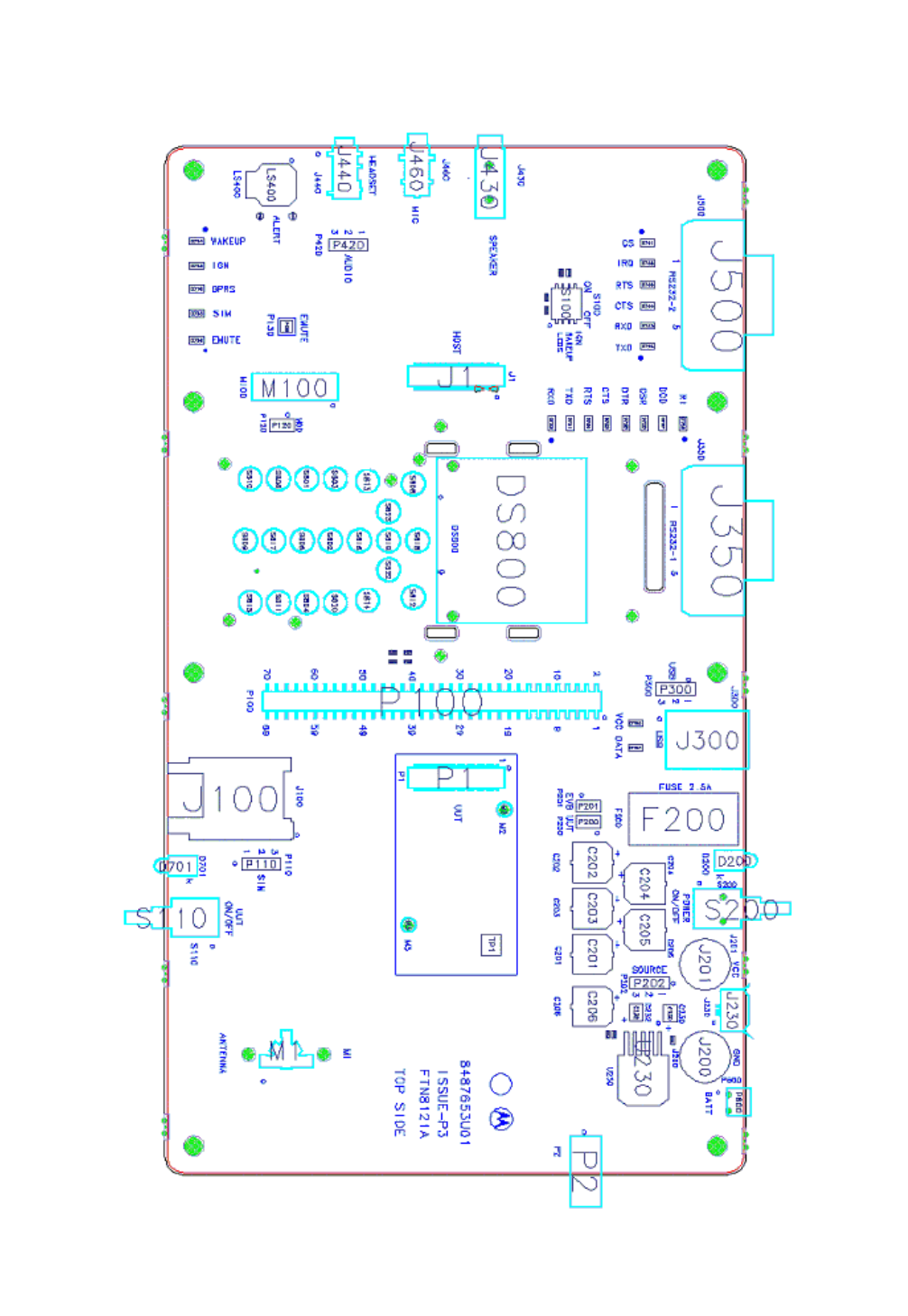
6.2 DEVELOPERS BOARD PLACEMENT
Figure 16 shows the top layout of the Developer Board:
Figure 16. Developer Board Top Layout
DRAFT 1 (31.3.03)
Schematics, Placement and Parts List
42 98-08901C64-O
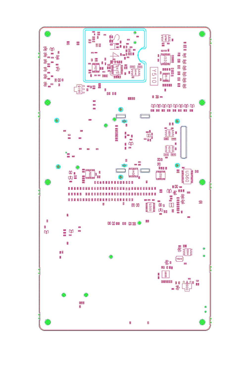
Figure 17 shows the bottom layout of the Developer Board:
Figure 17. Developer Board Bottom Layout
DRAFT 1 (31.3.03)

98-08901C64-O 43
Schematics, Placement and Parts List
6.3 DEVELOPER BOARD PARTS LIST
Table 24. Developer Board Parts List
REFERENCE
SYMBOL
MOTOROLA
PART NO. DESCRIPTION
Resistors
R440 0662057A21 RES, 68
R600 0662057A22 RES, 75
R330 0662057A25 RES, 100
R773 0662057A28 RES, 130
R723, R725,
R745, R747
0662057A31 RES, 180
R703 0662057A35 RES, 270
R705, R707,
R709-10,
R713,
R717-18,
R727, R729,
R731, R733,
R735, R737,
R743, R749,
R751, R753,
R763, R764
0662057A36 RES, 300
R203 0662057A39 RES, 390
R603 0662057A47 RES, 820
R604 0662057A49 RES, 1K
R602 0662057A51 RES, 1.2K
R312 0662057A53 RES, 1.5K
R465-66 0662057A57 RES, 2.2K
R201-2, R702,
R704, R706,
R708,
R711-12,
R716, R722,
R724, R726,
R728, R730,
R732, R734,
R736, R742,
R744, R746,
R748, R750,
R752,
R760-61,
R800
0662057A65 RES, 4.7K
R179, R197,
R200, R303,
R414-16,
R441, R508-9,
R525, R601,
R607, R774,
R781
0662057A73 RES, 10K
R230-32,
R322
0662057A75 RES, 12K
DRAFT 1 (31.3.03)

Schematics, Placement and Parts List
44 98-08901C64-O
R411-12,
R418
0662057A80 RES, 20 K
R177-78,
R191-92,
R196, R198,
R317-18,
R320-21,
R353, R507,
R608-9, R780
0662057A89 RES, 47 K
R435 0662057A97 RES, 100 K
R1, R10-11,
R15-16, R107,
R116-144,
R146,
R148-49,
R151-53,
R155, R157,
R159, R170,
R172-76,
R181-190,
R300-302,
R350-352,
R400-402,
R407-410,
R413, R417,
R419,
R423-27,
R460,
R480-85,
R500-503,
R506,
R510-524,
R594-97,
R606,
R611-618,
R700, R720,
R740,
R770-771,
R801-805
0662057B47 RES, 0
R790 0662057C01 RES, 0
R430-31,
R433-34
0662057P20 RES, 20K
R221 0662057P95 RES, 100K
R234 0662057P96 RES, 130K
R211, R220,
R241
0662057P97 RES, 150K
R210, R240 0662057P99 RES, 200K
R233 0662057T17 RES, 301K
R310-11 0662057T43 RES, 33.2
R772 0662057W13 RES, 3.3
Table 24. Developer Board Parts List (Continued)
REFERENCE
SYMBOL
MOTOROLA
PART NO. DESCRIPTION
DRAFT 1 (31.3.03)

98-08901C64-O 45
Schematics, Placement and Parts List
Fuses
F200 0904923K01 FUSE
F600 6586221J04 FUSE
Connectors
J430 0909032K01 CONN_J
J460 0909399T09 CONN_J
J350, J500 0909672B03 CONN_J
P2 0909908P02 CONN_J
J1 0987547V01 CONN_J
J300 0987583U01 CONN_J
J440 0987837L02 CONN_J
J230 0989601K01 CONN_J
Capacitors
C1, C2, C3,
C4
2113740F01 CAP, 0.5p
C5 2113740F19 CAP, 4.7p
C207, C215,
C217, C234
2113740F25 CAP, 8.2p
C442, C444,
C447, C450,
C462,
C472-473
2113740F27 CAP, 10p
C100,
C102-106,
C108-115,
C130, C137,
C143,
C147-151,
C153-160,
C171,
C191-192,
C211, C221,
C241, C312,
C401-404,
C416-418,
C421-428,
C436-439,
C443,
C445-446,
C448-449,
C451-2, C461,
C463-4,
C470-471,
C474-475,
C502-510,
C781,
C810-819
2113740F39 CAP, 33p
Table 24. Developer Board Parts List (Continued)
REFERENCE
SYMBOL
MOTOROLA
PART NO. DESCRIPTION
DRAFT 1 (31.3.03)

Schematics, Placement and Parts List
46 98-08901C64-O
C125, C128,
C131, C134,
C208, C216,
C218, C231,
C511-12
2113740F41 CAP, 39p
C411-412,
C414
2113741F49 CAP, 10n
C101, C107,
C116-124,
C126-127,
C129,
C132-133,
C135-136,
C138-142,
C144-146,
C152, C465,
C600
2113743E20 CAP, 100n
C430-431,
C433-434
2113743K16 CAP, 220n
C361-364,
C521-524
2113743K17 CAP, 330n
C310, C313,
C466
2113928C04 CAP, 4.7u
C440-441 2113928C12 CAP, 10u
C170,
C172-173,
C180, C190,
C200, C233,
C300, C311,
C350, C360,
C400, C410,
C413, C415,
C420, C432,
C435, C453,
C460, C500,
C513, C520,
C700, C720,
C770-774,
C780,
C800-801
2113928P04 CAP, 1u
C230, C232 2311049A57 CAPP, 10u
C210, C212,
C220, C222,
C240, C242
2311049A72 CAPP, 10u
C201-206 2387572V01 CAPP, 1000u
Inductors
L440 2409154M42 IDCTR, 33n
Shields
SH400 2604044K01 SHIELD
Table 24. Developer Board Parts List (Continued)
REFERENCE
SYMBOL
MOTOROLA
PART NO. DESCRIPTION
DRAFT 1 (31.3.03)

98-08901C64-O 47
Schematics, Placement and Parts List
Connectors
P130 2880001R01 CONN_P
P120,
P200-201
2880001R02 CONN_P
P110, P202,
P300, P420
2880001R03 CONN_P
P600 2886290J07 CONN_P
P100 2886397J02 CONN_P
P1 2887548V01 CONN_P
J201 2987604U01 CONN_J
J200 2987604U02 CONN_J
Contacts
M1 3903920K01 CONTACT
Switches
S200 4008241G06 SWITCH_ET01
S110 4008242G05 SWITCH
J100 4009060S03 SWITCH_CONTACT_BLOCK
S100 4080564C02 SWITCH
Spacers
M2, M3, M4,
M5, M6, M7,
M8, M9
4302809C15 SPACER
LEDs
D702-704,
D708, D710,
D721-8,
D741-746,
D760-761
4805729G44 BR1102W
D770-771 4870370A25 CL-260S-WA
D200, D701 4880304L02 LED_RED
Transistors
Q701-704,
Q706, Q708,
Q710,
Q760-761
4809579E16 TN0200T
Q705, Q707,
Q711,
Q721-728,
Q741-746
4809579E18 TP0101T
Q200, Q780 4809807C31 IRF7220
Q350, Q720,
Q740, Q1000
4809939C05 UMC5NTL
Table 24. Developer Board Parts List (Continued)
REFERENCE
SYMBOL
MOTOROLA
PART NO. DESCRIPTION
DRAFT 1 (31.3.03)

Schematics, Placement and Parts List
48 98-08901C64-O
Q110, Q300,
Q500, Q610,
Q620, U771
4813824A10 MMBT3904
Q201 4813824A17 MMBT3906
Q600 4813824B11 MMJT9435
Q190 4813824B13 MMJT9410T1
Diodes
VR200 4813831A14 SMB5918
D320 4813833C02 MMBD6100
VR100-105,
VR310
4886182U05 UMZ6.8EN
Integrated Circuits
U510 5102870C15 MAX3100EEE
U201, U220,
U240
5104187K10 MAX604ESA
U230 5104187K89 MIC29302BU
U370, U380,
U530
5105492X05 TC7SH32
U520 5108428S67 MAX3223EAP
U330 5109522E53 NC7SZ125
U360 5109781E76 MAX3238
U320 5109817F26 TC54VN2902E
U420 5113805B39 MC74HC4053
U410 5113811A56 MC145481
U300, U350,
U400, U500
5113837A07 MC74LCX244
U430 5186214J87 TPA6203A1GQVR
U600 5187970L09 LM3652
U310 5187970L15 ISP1104
U770 5187970L20 LM2795BLX
General
M100 5987772L02 MOTOR
Y510 4884450T02 XTAL3_6864MHZ
LS400 5087951K01 SPKR
Table 24. Developer Board Parts List (Continued)
REFERENCE
SYMBOL
MOTOROLA
PART NO. DESCRIPTION
DRAFT 1 (31.3.03)
98-08901C64-O 49
7. ERRATA
7.1 SWITCH ASSIGNMENTS CORRECTION
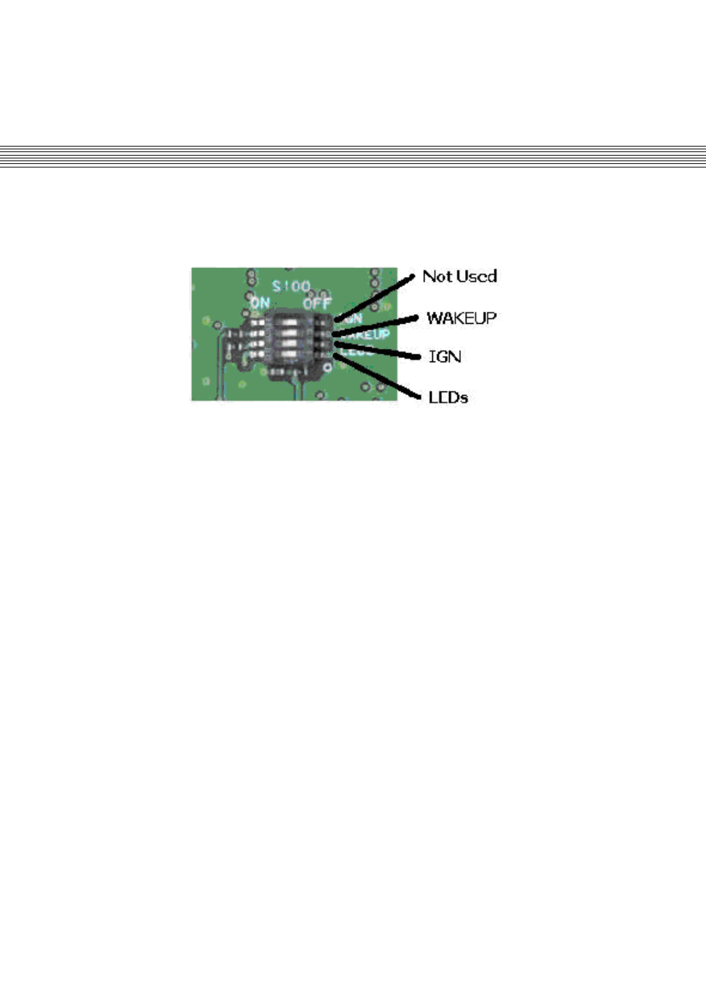
The S100 options switch on the Developer Board is labeled incorrectly. Figure 18 shows the correct function of each switch.
PLEASE PROVIDE A PICTURE WITHOUT CALLOUTS.
Figure 18. S100 Options Switch Functions
DRAFT 1 (31.3.03)

Errata
50 98-08901C64-O
DRAFT 1 (31.3.03)

98-08901C64-O 51
8. INDEX
DRAFT 1 (31.3.03)

Index
52 98-08901C64-O
DRAFT 1 (31.3.03)

REVISION HISTORY
Revision Date Purpose
DRAFT 1 (31.3.03)

March 2003
© Motorola Inc., 2003 98-08901C66-O
g20 Cellular Engine
Module Description
CONTENTS
REVISION HISTORY ................................................................................................................................................................ii
PREFACE
1.1 SCOPE OF THIS MANUAL .................................................................................................................................................1
1.2 WHO SHOULD USE THIS MANUAL.................................................................................................................................1
1.3 APPLICABLE DOCUMENTS ..............................................................................................................................................1
1.3.1 Documents...................................................................................................................................................................1
1.3.2 Standards.....................................................................................................................................................................1
1.4 HOW THIS MANUAL IS ORGANIZED..............................................................................................................................1
INTRODUCTION
2.1 GENERAL DESCRIPTION...................................................................................................................................................3
2.2 TERMS AND ABBREVIATIONS ........................................................................................................................................3
2.3 PRODUCT SPECIFICATIONS.............................................................................................................................................5
2.4 MODELS DESCRIPTION.....................................................................................................................................................7
2.5 REGULATORY APPROVALS.............................................................................................................................................7
2.6 REGULATORY STATEMENT.............................................................................................................................................7
2.7 SAFETY PRECAUTIONS.....................................................................................................................................................7
2.7.1 User Operation ............................................................................................................................................................7
2.7.2 Antenna Installation ....................................................................................................................................................8
HARDWARE DESCRIPTION
3.1 G20 BLOCK DIAGRAM DESCRIPTION AND OPERATION OVERVIEW ....................................................................9
3.1.1 g20 Block Diagram .....................................................................................................................................................9
3.1.2 Basic RS232 and Analog Audio Connectivity..........................................................................................................11
3.1.3 Basic RS232 and Digital Audio Connectivity...........................................................................................................11
3.1.4 Additional Recommended Connections....................................................................................................................12
3.1.5 G20 for Handset Configuration.................................................................................................................................13
3.2 POWER SUPPLY AND CURRENT CONSUMPTION .....................................................................................................13
3.2.1 Power Supply Design................................................................................................................................................13
3.2.2 G20 Current Consumption ........................................................................................................................................14
3.2.3 Turning the Unit On/Off ...........................................................................................................................................15
DRAFT 1 (31.3.03)

iv 98-08901C66-O
3.2.4 Sleep Mode Options ................................................................................................................................................. 16
3.3 COMMUNICATION INTERFACES.................................................................................................................................. 18
3.3.1 RS232 ....................................................................................................................................................................... 18
3.3.2 USB .......................................................................................................................................................................... 20
3.3.3 SIM........................................................................................................................................................................... 21
3.3.4 SPI ............................................................................................................................................................................ 22
3.3.5 Unique g20 Interfaces............................................................................................................................................... 22
3.4 AUDIO INTERFACES........................................................................................................................................................ 23
3.4.1 Analog Audio Interfaces........................................................................................................................................... 23
3.4.2 Digital Audio Interface............................................................................................................................................. 27
3.5 ANTENNA........................................................................................................................................................................... 28
3.5.1 Antenna Performance Recommendations ................................................................................................................ 28
3.6 CHARGER INTERFACE.................................................................................................................................................... 28
3.7 DISPLAY INTERFACE...................................................................................................................................................... 28
3.8 ESD PROTECTION ............................................................................................................................................................ 29
CONNECTOR PIN
ASSIGNMENTS
4.1 CONNECTORS ................................................................................................................................................................... 31
4.2 PIN ASSIGNMENTS .......................................................................................................................................................... 31
MECHANICAL DESCRIPTION
5.1 MECHANICAL DETAILS.................................................................................................................................................. 37
SERVICE SUPPORT
6.1 CUSTOMER ASSISTANCE............................................................................................................................................... 39
6.2 TESTING A STANDALONE UNIT................................................................................................................................... 39
6.3 TROUBLESHOOTING....................................................................................................................................................... 39
6.4 PROGRAMMING ............................................................................................................................................................... 39
INDEX
DRAFT 1 (31.3.03)

98-08901C66-O v
LIST OF FIGURES
Figure 1. g20 Block Diagram .......................................................................................................................................................9
Figure 2. Basic RS232 and Analog Audio Connectivity............................................................................................................11
Figure 3. Basic RS232 and Digital Audio Connectivity.............................................................................................................12
Figure 4. Additional g20 Connectivity .......................................................................................................................................12
Figure 5. g20 for Handset Configuration....................................................................................................................................13
Figure 6. VCC Signal During TX Periods..................................................................................................................................14
Figure 7. On/Off Signal Timing Diagram ..................................................................................................................................15
Figure 8. CTS Sleep Mode Timing.............................................................................................................................................16
Figure 9. DCE/DTE Connectivity ..............................................................................................................................................17
Figure 10. Waking Up the g20 when the DTE Wants to Send Data ..........................................................................................17
Figure 11. Waking Up the DTE when the g20 Wants to Send Data ..........................................................................................18
Figure 12. g20 RS232 Interface..................................................................................................................................................18
Figure 13. RS232 Connection.....................................................................................................................................................19
Figure 14. g20 USB Connection for g20 Models with a USB Driver........................................................................................20
Figure 15. g20 USB Connection for g20 Models without a USB Driver...................................................................................21
Figure 16. g20 SIM Connection .................................................................................................................................................21
Figure 17. TX_EN Transmission................................................................................................................................................22
Figure 18. Antenna-detect Circuit ..............................................................................................................................................23
Figure 19. GPRS-detect Coverage Indication.............................................................................................................................23
Figure 20. SPKR_N Output Configuration.................................................................................................................................24
Figure 21. Mechanical Mounting Requirements ........................................................................................................................37
DRAFT 1 (31.3.03)

vi 98-08901C66-O
LIST OF TABLES
Table 1. Terms and Abbreviations ............................................................................................................................................... 3
Table 2. Product Specifications.................................................................................................................................................... 5
Table 3. g20 Models..................................................................................................................................................................... 7
Table 4. g20 Current Consumption............................................................................................................................................ 14
Table 5. SPI Pinout..................................................................................................................................................................... 22
Table 6. SPKR_N Output when g20 Set to Maximum Volume Level and Headset Interrupt is Low....................................... 24
Table 7. SPKR_N Output when g20 Set to Maximum Volume Level and Headset Interrupt is Not Low................................ 25
Table 8. SPKR_N Output when a 500mV RMS Signal is Transmitted..................................................................................... 25
Table 9. SPKR_N Output when g20 is in Handset Mode.......................................................................................................... 26
Table 10. SPKR_N Output when g20 is in Headset Mode........................................................................................................ 26
Table 11. Alert Transducer Levels for the ALERT_P Signal.................................................................................................... 27
Table 12. Antenna Performance Recommendations.................................................................................................................. 28
Table 13. g20 Interface Connector Pin Assignments................................................................................................................. 31
DRAFT 1 (31.3.03)

98-08901C64-O 1
1. PREFACE
1.1 SCOPE OF THIS MANUAL
This manual introduces the g20 embedded module and describes the technical details required by the data terminal equipment
(DTE) team to successfully integrate the Motorola g20 cellular engine into an original equipment manufacturer (OEM) wireless
host device.
We at Motorola want to make this guide as helpful as possible. Keep us informed of your comments and suggestions for
improvements.
You can reach us by Email at: GSM support-BSH015@email.mot.com.
1.2 WHO SHOULD USE THIS MANUAL
This manual is intended for all members of the DTE OEM integration team who are responsible for integrating the c18 module
into the host OEM device, including representatives from hardware, software and RF engineering disciplines.
1.3 APPLICABLE DOCUMENTS
PLEASE PROVIDE DETAILS FOR THIS SECTION.
1.3.1 Documents
g20 Developer’s Kit - 9808901C67-O
g20 AT Commands - 9808901C68-O
1.3.2 Standards
PLEASE PROVIDE DETAILS FOR THIS SECTION.
1.4 HOW THIS MANUAL IS ORGANIZED
This manual contains the following chapters:
•Chapter 1 contains this Preface.
•Chapter 2 introduces the g20 unit and provides important safety instructions.
•Chapter 3 provides a detailed hardware description of the blocks and components comprising the g20.
•Chapter 4 describes the pin assignments for g20 connectors.
•Chapter 5 describes mechanical requirements for the g20 unit.
•Chapter 6 provides contact information for Motorola Service Support and Customer Assistance, as well as valuable
troubleshooting and programming information.
DRAFT 1 (31.3.03)

Preface
2 98-08901C64-O
DRAFT 1 (31.3.03)
98-08901C64-O 3
2. INTRODUCTION
2.1 GENERAL DESCRIPTION
The g20 is Motorola’s newest family of embedded cellular products. Motorola continues its tradition of excellence by
introducing this new cellular engine family for GSM/GPRS communications, consisting of the d10, the d15 and the g18.
The new module is similar to a condensed cellular phone core, and can be integrated in any system or product that needs to
transfer voice or data information. Thus, it significantly enhances the system’s capabilities, transforming it from a standalone,
isolated product to a powerful component connected to communication nets.
The new g20 is extremely small in dimensions, yet packed with a host of highly-advanced features designed to facilitate fast
and easy integration with OEM user products. It significantly shortens the development process for OEM developers, thanks to
its wide range of built-in applications, and minimizes the product’s time to market.
The g20 module is ideally suited for the automotive, telemetry, security, insurance and EPOS industries, for delivery and
handheld terminals, and for PDA markets.
2.2 TERMS AND ABBREVIATIONS
This section provides definitions for terms and acronyms used in this document.
Table 1. Terms and Abbreviations
Acronym/Term Definition/Description
AOC Automatic Output Control
BABT British Approval Board - Telecommunications
CSD Circuit-switched Data
DCE Data Communication Equipment (such as modems)
DCS Digital Cellular System (GSM in the 1800MHz band)
DOC Department of Communications (Canada)
DSP Digital Signal Processor
DTE Data Terminal Equipment (such as terminals, PCs and so on)
DTMF Dual-Tone Multi-Frequency
EGSM Extended Global System for Mobile Communications
EIRP Effective Isotropic Radiated Power
EMC WHAT DOES THIS STAND FOR?
EOTD Enhanced Observed Time Difference
EPOS Electronic Point of Sale
ERP Effective Radiated Power
ESD Electrostatic Discharge
FCC Federal Communications Commission (U.S.)
FTA Foreign Telecommunication Administration
DRAFT 1 (31.3.03)

Introduction
4 98-08901C64-O
GCF WHAT DOES THIS STAND FOR?
GPIO General Purpose Input/Output
GPRS General Packet Radio Service
GSM Global System for Mobile Communications
IC Integrated Circuit
LNA Low-noise Amplifier
MMCX Multimedia Communications Exchange
MO Mobile Originated
MT Mobile Terminated
OEM Original Equipment Manufacturer
PCB Printed Circuit Board
PCM Pulse Code Modulation
PCS Personal Communication System (also known as CDMA 1900)
PDA Personal Data Assistant
PDU Packet Data Unit
PLL Phase-locked Loop
PTCRB PCS-1900 Type Certification Review Board (GSM North America)
R&TTE Radio and Telecommunications Terminal Equipment
RMS Root Mean Square
RTS Request To Send
SAR Segmentation and Reassembly
SIM Subscriber Identity Module
SMS Short Message Service
SPI Serial Peripheral Interface
TDMA Time Division Multiple Access
UART Universal Asynchronous Receiver Transmitter
USB Universal Serial Bus
USSD Unstructured Supplementary Services Data
VCC Voltage Common Collector
VSWR Voltage Standing Wave Ratio
Table 1. Terms and Abbreviations (Continued)
Acronym/Term Definition/Description
DRAFT 1 (31.3.03)
98-08901C64-O 5
Introduction
2.3 PRODUCT SPECIFICATIONS
Table 2. Product Specifications
Product Features
Operating systems: EGSM: 900/1800 MHz
GSM: 850/1900 MHz
Physical Characteristics
Size: Size: 24.4 x 48.2 x 6.0 mm
Mounting: Two 2.2 mm holes
Weight: 11.9 grams
Environmental
Operational temperature: -20°C +60°C
Functional temperature: -20°C +70°C
Storage temperature: -40°C +85°C
Performance
Operating voltage: Voltage: 3.0 - 4.2 V
Current consumption: < 2.5 mA @ DRX9 (Idle mode)
Tx power: • 0.6 W, 850 MHz
• 2 W, 900 MHz
• 1 W, 1800/1900 MHz
Interfaces
Connectors: • Single 70-pin, board-to-board
•RF MMCX
SIM Card: • Local SIM connectivity
• 32K SIM
• 1.8/3.0 V
Serial: • RS232:
• BR from 300 bps to 115 Kbps
• Auto BR from 300 bps to 115 Kbps
•USB
• 12 Mbps USB specifications, Rev. 1.1
Data Features
GPRS: • Multi-slot class 8 (4 down; 1 up)
• Max BR 85.6 Kbps
• Class B GSM 07.10 multiplexing protocol
• Coding scheme CS1-CS4
CSD: Max BR 14.4 Kbps
SMS: • MO/MT Text and PDU modes
• Cell broadcast
FAX Class 1
Voice Features
Telephony
Digital audio
Differential analog audio lines
DRAFT 1 (31.3.03)

Introduction
6 98-08901C64-O
Voice Features (Continued)
Vocoders EFR/ER/FR/AMR
DTMF support
Audio control: echo cancellation, noise suppression, side tone and gain control
GSM Supplementary Service
USSD Phase II
Call forwarding
Call hold, waiting and multiparty
Call diverting
Missed-call indicator
AOC
Call barring
Character Set
UTF8
UCS2
Control/Status Indicators
GPRS coverage
Wakeup
Antenna detect
TX enable
Reset
Entertainment mute
Features over RS232
Embedded TCP/IP stack
STK Class II
User Application
Application Programming Interface (API)
12 GPIO lines
2 A/D lines
Emergency and Location
FCC E911 Phase II Location Mandate using EOTD
AT Command Set
GSM 07.05
GSM 07.07
Motorola proprietary AT commands
Accessories
Firmware data loader
Data logger
Developer Kit
Note
Specifications are subject to change without prior notice.
Table 2. Product Specifications (Continued)
DRAFT 1 (31.3.03)
98-08901C64-O 7
Introduction
2.4 MODELS DESCRIPTION
Table 3 lists the available g20 models.
2.5 REGULATORY APPROVALS
The following regulatory approvals apply for the g20 module:
•FTA, FCC, DOC, PTCRB
•R&TTE
•GCF
•EMC
•BABT
•QS9000 manufacturing
2.6 REGULATORY STATEMENT
WE NEED SOURCE MATERIAL FOR THIS SECTION.
2.7 SAFETY PRECAUTIONS
2.7.1 User Operation
Do not operate your telephone when a person is within 8 inches (20 centimeters) of the antenna. A person or object within 8
inches (20 centimeters) of the antenna could impair call quality and may cause the phone to operate at a higher power level than
necessary.
IMPORTANT: The telephone must be installed in a manner that provides a minimum separation distance of
20 cm or more between the antenna and persons to satisfy FCC RF exposure requirements for mobile transmitting devices.
IMPORTANT: To comply with the FCC RF exposure limits and satisfy the categorical exclusion requirements for mobile
transmitters, the following requirements must be met:
Table 3. g20 Models
Model Operating Bands Interface Connectors Serial Interface
F3001 GSM 850/1900 •70-pin 0.5 mm pitch
•MMCX RF connector RS232
F3002 EGSM 900/1800 •70-pin 0.5 mm pitch
•MMCX RF connector RS232
F3003 GSM 850/1900 •70-pin 0.5 mm pitch
•MMCX RF connector USB
F3004 EGSM 900/1800 •70-pin 0.5 mm pitch
•MMCX RF connector USB
DRAFT 1 (31.3.03)

Introduction
8 98-08901C64-O
2.7.2 Antenna Installation
•A minimum separation distance of 20 cm needs to be maintained between the antenna and all persons, otherwise a SAR test
will be required.
• The transmitter effective radiated power must be less than 1.5 Watts ERP (2.45 Watts or 33.9 dBm EIRP). This requires that
the combination of antenna gain and feed line loss does not exceed 11 dBi.
DRAFT 1 (31.3.03)
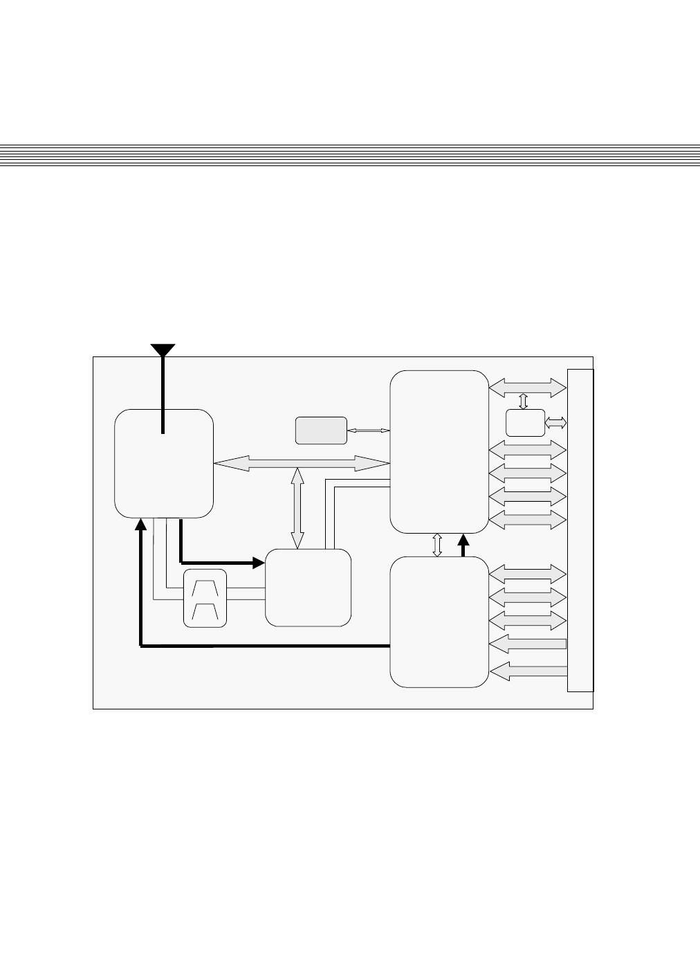
98-08901C64-O 9
3. HARDWARE DESCRIPTION
3.1 G20 BLOCK DIAGRAM DESCRIPTION AND OPERATION OVERVIEW
This chapter describes the basic blocks comprising the g20 module and the connectivity options for the module.
3.1.1 g20 Block Diagram
Figure 1 shows a block diagram for the g20 module:
Figure 1. g20 Block Diagram
The g20 consists of the following blocks:
•Power and Audio Management IC: This block is responsible for the power on/off process, analog audio drivers, internal
regulators, realtime clock activities, and the battery charging process. When an On command is received, this IC wakes up
the internal regulators and controls the reset process. This activity turns the unit on. When an Off command is received, this
IC sends the request to the main processor, which in turn shuts down the unit in an orderly fashion. During shutdown, the
unit is disconnected from the network, all tasks are terminated and the regulators are shut down. The on/off inputs (On/Off
and Ignition) are always on, even when the unit is off.
Transmitter
IC
Main
Processor
&
DSP
Memories
Power & Audio
Management IC
Receiver
IC
Control
Serial
USB
Driver
PCM
SIM
GPIO
SPI
ADC
Audio
Charger
Power
Interface Connector
G20
Ant
On/Off / IGN
DRAFT 1 (31.3.03)

Hardware Description
10 98-08901C64-O
•Main Processor and DSP: This block is responsible for all the main tasks in the unit. This block contains the following
components:
•Main processor
•DSP for controlling speech options
•UART
•USB block
•Digital audio driver
•SIM card
•Two SPI buses (one internal and one externally accessible)
•Main clock (26 MHz)
•Address/data buses
•RF PLL
•Controller to the RF ICs, which is the heart of the unit
This module provides the following connectivity:
•Address/data bus
•UART to the user connector
•USB via an optional USB driver to the user connector
•Digital audio (PCM) to the user connector
•SIM card interface
•SPI to the user connector
•SPI to control the RF ICs
•Control signals to the power amplifier IC
•Handshake with the Power and Audio Management IC
•General I/O to the user connector
•Receiver Block: This block is an RF block that contains all the receiver channels. It contains the following components:
•Front filters
•LNAs
•Mixers
•VCOs
•I/Q outputs
•Control signals
•Transmitter Block: This is an RF block that contains all the transmitter channels. It contains the following components:
•Power amplifiers
•Power control loop
•Antenna switch
•Harmonic filter
•Input buffers
•Control signals
•Antenna connection
DRAFT 1 (31.3.03)
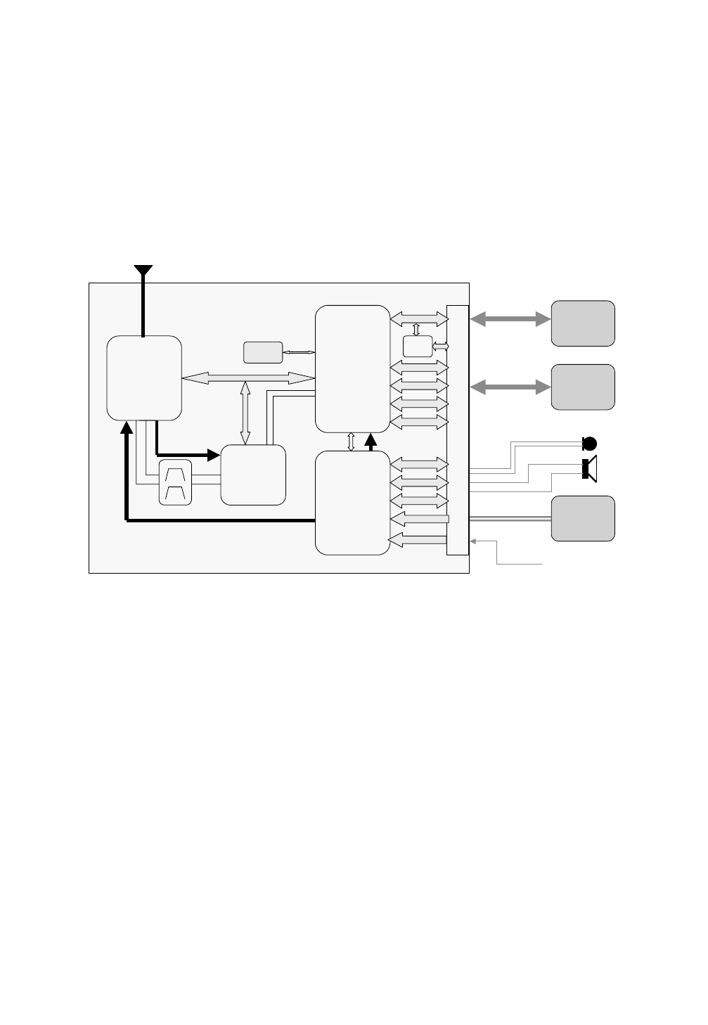
98-08901C64-O 11
Hardware Description
3.1.2 Basic RS232 and Analog Audio Connectivity
The following basic g20 connectivity requirements apply for UART (RS232) and analog audio connections (see Figure 2 for
reference):
•The RS232 is connected via eight pins to the g20.
•The SIM card is connected via five pins to the SIM driver of the g20.
•The microphone is connected via two pins to the g20 (Mic and Mic Ground).
•The Speaker is connected via two differential lines to the g20.
•The power supply is connected via eight pins (four VCC and four Ground) to the g20.
•The On/Off or Ignition pin is connected.
Figure 2. Basic RS232 and Analog Audio Connectivity
3.1.3 Basic RS232 and Digital Audio Connectivity
The following basic g20 connectivity requirements apply for UART (RS232) and digital audio connections (see Figure 3 for
reference):
•The RS232 is connected via eight pins to the g20.
•The SIM card socket is connected via five pins to the SIM driver of the g20.
•The DTE DSP is connected via five pins to the g20 (PCM).
•The power supply is connected via eight pins (four VCC and four Ground) to the g20.
•The On/Off or Ignition pin is connected.
DTE
UART
SIM
Socket
Transmitter
IC
Main
Processor
&
DSP
Memories
Power & Audio
Management IC
Receiver
IC
Control
Serial
USB
Driver
PCM
SIM
GPIO
SPI
ADC
Audio
Charger
Power
Interface Connector
G20
Ant
Power
Supply
Mic
SPKR
On/Off or
Ignition
On/Off - IGN
DRAFT 1 (31.3.03)
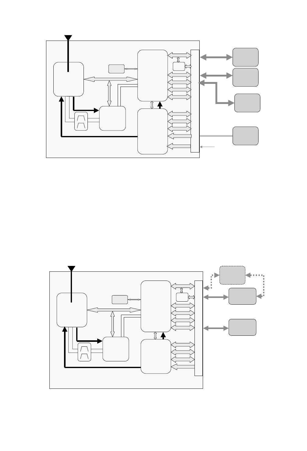
Hardware Description
12 98-08901C64-O
Figure 3. Basic RS232 and Digital Audio Connectivity
3.1.4 Additional Recommended Connections
Additional g20 connectivity options are described below (see Figure 4 for reference):
•A USB connector that is connected via three lines to the g20. In this case, when USB is used, the DTE UART should be in
tri-state (high impedance).
•A USB connector that is connected via a USB driver to the g20 (in g20 models without a USB driver). When USB is used,
the DTE UART should be in tri-state (high impedance).
•An SPI block that is connected via four pins to the g20 (for debug accessibility).
Figure 4. Additional g20 Connectivity
Transmitter
IC
Main
Processor
&
DSP
Memories
Power & Audio
Management IC
Receiver
IC
Control
Serial
USB
Driver
PCM
SIM
GPIO
SPI
ADC
Audio
Charger
Power
Interface Connector
G20
DTE
UART
SIM
Socket
Ant
Power
Supply
DTE
DSP
On/Off / IGN On/Off or IGN
Transmitter
IC
Main
Processor
&
DSP
Memories
Power & Audio
Management IC
Receiver
IC
Control
Serial
USB
Driver
PCM
SIM
GPIO
SPI
ADC
Audio
Charger
Power
Interface Connector
G20
USB
Driver
Ant
USB
Connector
SPI
Device
DRAFT 1 (31.3.03)
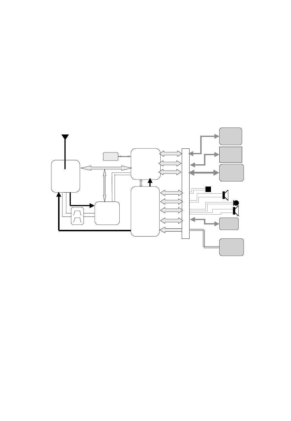
98-08901C64-O 13
Hardware Description
3.1.5 G20 for Handset Configuration
g20 connectivity when using the g20 as a cellular phone engine is described below (see Figure 5 for reference):
•The display is connected via five pins to the g20.
•The keypad is connected via eight pins to the g20.
•The SIM card socket is connected via five pins to the g20 SIM driver.
•The charger is connected via six pins (Interface to National LM3652) to the g20.
•The microphone is connected via two pins (Mic and Mic Ground) to the g20.
•The speaker is connected via two differential lines to the g20.
•The alert device is connected via two differential lines to the g20.
•The vibrator is connected via one pin to the g20.
•The battery is connected to the charger, and the charger is connected to the VCC and Ground pins.
Figure 5. g20 for Handset Configuration
3.2 POWER SUPPLY AND CURRENT CONSUMPTION
This section describes the following power-related considerations for the g20:
•Power supply design
•g20 current consumption
•Turning the unit on/off
•Sleep mode options
3.2.1 Power Supply Design
The following power supply design considerations apply to the g20:
•The g20 is designed to operate between 3.0 V to 4.2 V on the g20 input (after all losses). In order to reduce battery power
consumption, it is important to verify power supply line and regulator losses in the PCB.
•The g20 is a GSM/GPRS phone that transmits in 0.5 ms pulses every 4.6 ms. The peak current is approximately 2.0 A.
Transmitter
IC
Main
Processor
&
DSP
Memories
Power & Audio
Management IC
Receiver
IC
Control
Display
SIM
Audio
Charger
Power
Interface Connector
G20
Display
SIM
Socket
Ant
Battery
Mic
SPKR
Key Pad
Alert
Vibrator Alert
Vibrator
Key Pad
Charger
DRAFT 1 (31.3.03)
Hardware Description
14 98-08901C64-O
•When the power supply is lower than 2.85 V, the g20 software determines that the battery is low and disconnects the unit.
•When the voltage is greater than 4.25 V, the g20 software detects an over voltage condition and does not allow the unit to
establish a call.
•The VCC line typically drops during TX periods.
Figure 6. VCC Signal During TX Periods
To minimize the ∆, it is recommended to use lines that are as short as possible, and to place a 1000uF capacitor (or the maximum
possible) in the g20 VCC input. (When a battery is used, there is no need for a large capacitor.)
It is recommended to keep the ∆ less than 0.3 V.
3.2.1.1 Power Supply RF Filtering
It is recommended to add RF filtering to the DC lines.
Use 100nF, 39pF, 22pF or 8.2pF capacitors in parallel to the power supply lines (close to the g20 connector). MUST ALL
THESE CAPACITORS BE USED IN PARALLEL? OR SOME COMBINATION?
3.2.2 G20 Current Consumption
In order to design the power supply correctly and to calculate the battery life, you should take into account the current
consumption of the g20 when operating in different modes.
Note
The power supply should be able to drive at least 2.5 A.
Table 4. g20 Current Consumption
Mode Current Consumption (mA RMS)
g20 in Sleep mode (camped and
Sleep-mode enabled) < 2.5 mA, RMS @ DRX9, Typical 2.2 mA
< 4.5 mA, RMS @ DRX2, Typical 3.5 mA
g20 during search time < 40 mA, RMS, Typical 25 mA, RMS
g20 off < 100 uA – Typical 25 uA
g20 during a call
GSM 900 @ Power level #5 < 350 mA, Typical 270 mA
@ Power level #10, Typical 160 mA
@ Power level #19, Typical 135 mA
TX TX TX
Transmit
Periods
VCC
DRAFT 1 (31.3.03)
98-08901C64-O 15
Hardware Description
3.2.3 Turning the Unit On/Off
Two different mechanisms are available to turn the g20 on and off:
•On/Off signal (Pin 53)
•Ignition line (Pin 51)
3.2.3.1 On/Off Signal
After power is applied to the g20, the on/off signal is pulled high to the VCC by a 200kΩ resistor.
To turn the g20 on, the on/off signal should be pulled low for a minimum of 700 ms.
After the g20 is turned on, the line should be pulled low for a minimum of 1.1 seconds to turn it off. The unit can be turned off
only if at least seven seconds have elapsed since turning it on.
Figure 7 shows the timing diagram for the on/off signal.
Figure 7. On/Off Signal Timing Diagram
In Figure 7, the following timing requirements apply:
•T1 minimum = 0.7 seconds.
•T2 minimum = 7 seconds.
•T3 minimum = 1.1 seconds.
GSM 850 @ Power level #7 < 250 mA, Typical 185 mA
@ Power level #10, Typical 160 mA
@ Power level #19, Typical 135 mA
DCS 1800 @ Power level #0 < 300 mA, Typical 220 mA
@ Power level #10, Typical 160 mA
@ Power level #19, Typical 135 mA
PCS 1900 @ Power level #5 < 300 mA, Typical 240 mA
@ Power level #10, Typical 160 mA
@ Power level #19, Typical 135 mA
Note
DRX2/9 is the rate used by the base station to query the mobile station. The network operator sets this parameter.
Table 4. g20 Current Consumption (Continued)
Mode Current Consumption (mA RMS)
T1 T2 T3
DRAFT 1 (31.3.03)
Hardware Description
16 98-08901C64-O
3.2.3.2 Ignition Line
When the g20 ignition line is held at a high level, the g20 is turned on. When this line is pulled low, the g20 is turned off. In
order to protect the line from voltage bounces, the g20 is tuned off only if the line is held low for at least 500 ms.
The high input to the ignition line must be greater than 2.75 V. The line can tolerate up to 40 V.
After the g20 is turned on, the application should wait for DSR before sending data to the g20. The DSR becomes active low
eight seconds after the start of T1, or after the ignition line is pulled high. DSR is only valid with UART, and is not valid with
USB.
3.2.4 Sleep Mode Options
This section describes how the g20 can be awakened by the DTE and vice-versa.
The DCE (g20) and the DTE can incorporate a sleep mechanism in their application in order to conserve battery life.
Sleep mode enables the g20 to be awakened when the DTE wants to communicate with it. Conversely, it also enables the DTE
to be awakened by the g20 when the g20 wants to communicate with it.
3.2.4.1 General
•The g20 Sleep Mode option can be enabled or disabled using ATS24.
•Sleep mode is activated by sending ATS24 = n, where n = 1, 2, 3 or 4 seconds. (To disable Sleep mode, send ATS24=0.)
•The g20 drops the CTS (h/w Flow Control) when it is in Sleep mode.
•The g20 does not enter Sleep mode when data is present on TXD or RXD lines.
•At the end of the TXD (meaning, the TXD buffer is empty), the g20 waits n seconds (as defined in ATS24 = n) before enter-
ing Sleep mode.
•The DTE uses CTS to send data only when the g20 is awake. The DTE waits when the g20 is in Sleep mode.
•The DTE should drop RTS during the sleep period in order to prevent the loss of data sent by the g20.
Figure 8. CTS Sleep Mode Timing
DRAFT 1 (31.3.03)
98-08901C64-O 17
Hardware Description
3.2.4.2 DCE/DTE Connectivity
Figure 9 shows DCE/DTE connectivity:
Figure 9. DCE/DTE Connectivity
Waking Up the DCE:
The following apply when waking up the DCE:
•The Wake-up In line is used to awaken the g20. This input is routed into an Interrupt in the g20.
•Whenever the Wake-up In line is at logic “low”, the g20 remains in an awake state.
•When the DTE needs to send data, it should activate this line, wait 30 ms (the wake time required for the g20), and then start
sending the data.
•While the DTE is sending data, the wake-up line should remain low, so that the g20 does not enter Sleep mode.
Figure 10. Waking Up the g20 when the DTE Wants to Send Data
Waking Up the DTE:
The following apply when waking up the DTE:
•The g20 uses the Wake-up Out line to indicate to the DTE that data is present.
•The DTE should not enter Sleep mode when the Wake-up Out line is low.
•When the g20 has data to send to the DTE, it drops the Wake-up Out line to low.
•The g20 will send the Wake-up Out line #ms to low, as indicated by S10x in Figure 11.
DTE TXD
Wake up
In line
30 ms 30 ms 30 ms
DRAFT 1 (31.3.03)
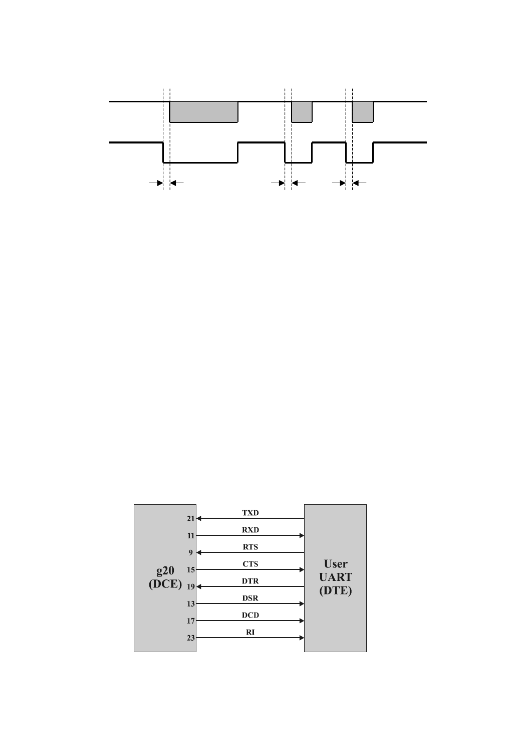
Hardware Description
18 98-08901C64-O
•While the g20 is sending data, the Wake-up Out line remains low.
•After the sending of data is completed, the g20 brings the Wake-up Out line to high.
•The DTE should keep RTS off during this sleep period in order to avoid sending data when it is not ready.
Figure 11. Waking Up the DTE when the g20 Wants to Send Data
3.3 COMMUNICATION INTERFACES
This section describes the following four interfaces that are available in the g20:
•RS232
•USB
•SIM
•SPI
3.3.1 RS232
The following apply when using
the RS2332 interface of the g20:
•The g20 supports full hard-
ware flow control (9 pins),
software flow control (Xon/
Xoff) and non-flow control.
•The g20 UART is connected directly to the interface connector.
•The g20 is a DCE device. Applicable line terminology is shown in Figure 12.
Figure 12. g20 RS232 Interface
RXD
Wake up Out
line
S10x ms S10x ms S10x ms
DRAFT 1 (31.3.03)
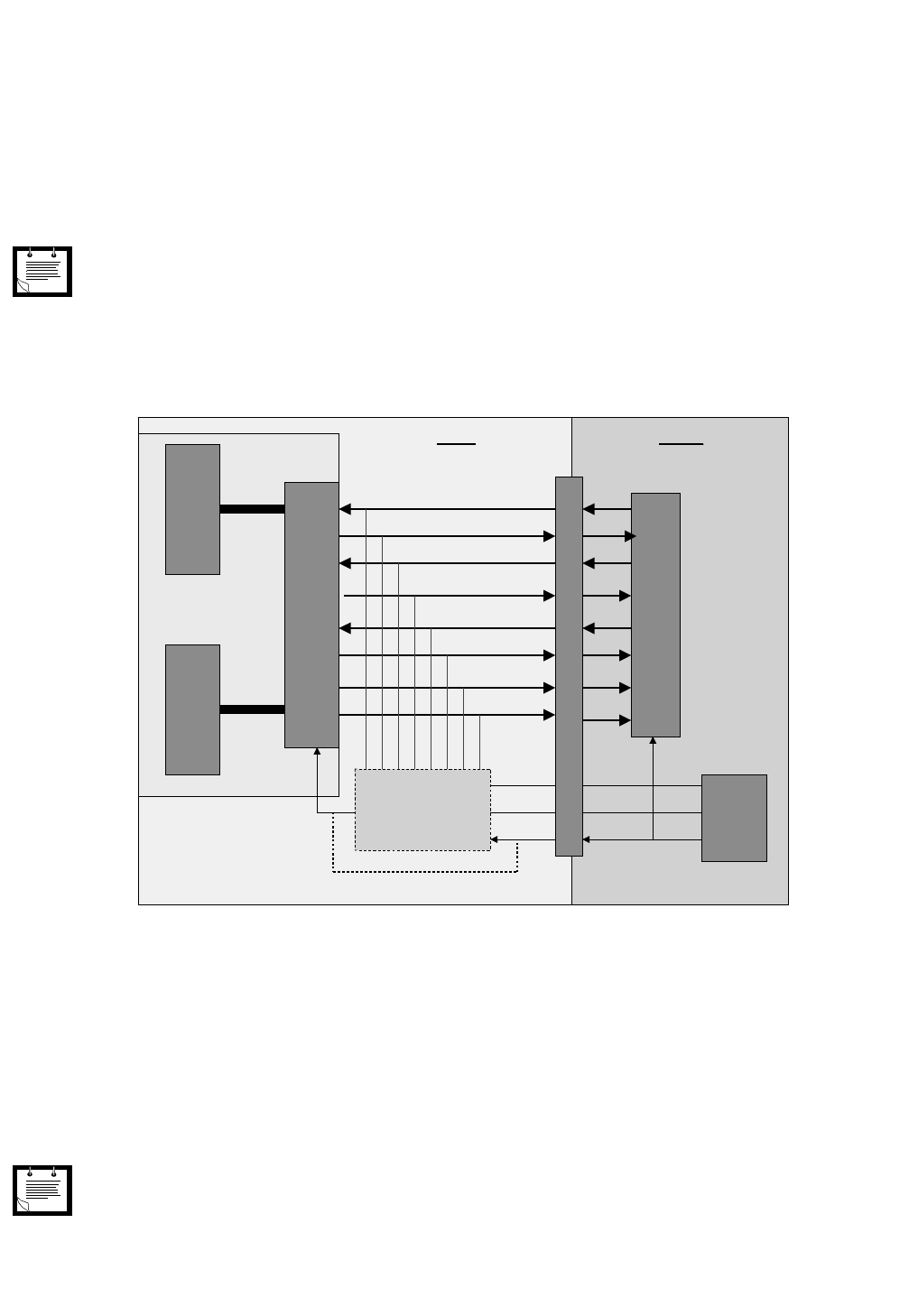
98-08901C64-O 19
Hardware Description
3.3.1.1 RS232 Levels
RS232 levels are as follows:
•Vih = 1.95 V minimum, 3.0 V maximum
•Vil = 0.8 V maximum
•Voh = 2.56 V minimum @ 100 uA
•Vol = 0.2 V maximum @ 100 uA
3.3.1.2 RS232 Connection
Figure 13 shows an RS232 connection diagram:
Figure 13. RS232 Connection
The following apply for g20 RS232 connections:
•The g20 can use both UART and USB connectors, but cannot use them both simultaneously.
•When USB is detected (by sensing the USB VBUS signal), the UART is disconnected from the g20 main processor pins and
USB functionality is added instead.
•The DTE should unload the RS232 lines when USB is used in order for the USB to function properly.
•RS232 signals are routed directly from the main processor to the connector.
Note
A buffer is required whenever DTE levels do not match g20 levels.
Note
In g20 models without a USB driver (F3001and F3002 models), RS232 signals can be used to connect an external
USB driver.
G20 Main
Processor
U
A
R
T
U
S
B
M
U
X
USB
Driver
D+
D-
USB VBUS
USB
Detect
TXD 21
RXD 11
RTS
CTS
DTR
DSR
DCD
RI
9
15
19
13
17
23
12
14
10
D
T
E
U
A
R
T
USB
connector
3 state
G20 DTE
DRAFT 1 (31.3.03)
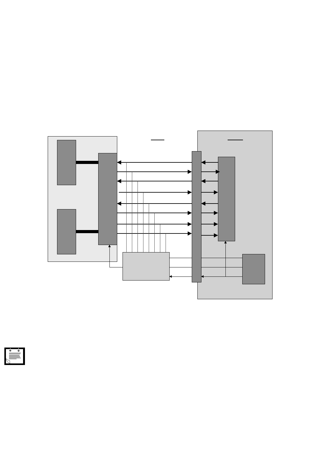
Hardware Description
20 98-08901C64-O
3.3.2 USB
The following apply for g20 USB connections:
•The g20 can use a USB port to communicate with a DTE device.
•The USB port is also used to load software into the g20. It is recommended to include connectivity to this port in the user
application.
•The g20 supports USB1.1 at a baud rate of 12 Mbps.
•The g20 supports two basic types, one with a USB driver (models F3003 and F3004), and one with the USB driver removed
(models F3001 and F3002).
3.3.2.1 USB Connection
Figure 14 shows g20 connection for g20 models with a USB driver:
Figure 14. g20 USB Connection for g20 Models with a USB Driver
As shown in Figure 14, the g20 USB is connected via three lines to the USB connector in the user application: D+, D- and USB
VBUS. When USB VBUS is applied, the g20 detects it and switches the main processor to USB mode.
Note
The DTE UART loads the USB driver/main processor lines. Therefore, the UART should be kept in tri-state.
G20 Main
Processor
U
A
R
T
U
S
B
M
U
X
USB
Driver
D+
D-
USB VBUS
USB
Detect
TXD 21
RXD 11
RTS
CTS
DTR
DSR
DCD
RI
9
15
19
13
17
23
12
14
10
D
T
E
U
A
R
T
USB
connector
3 state
G20 DTE
DRAFT 1 (31.3.03)
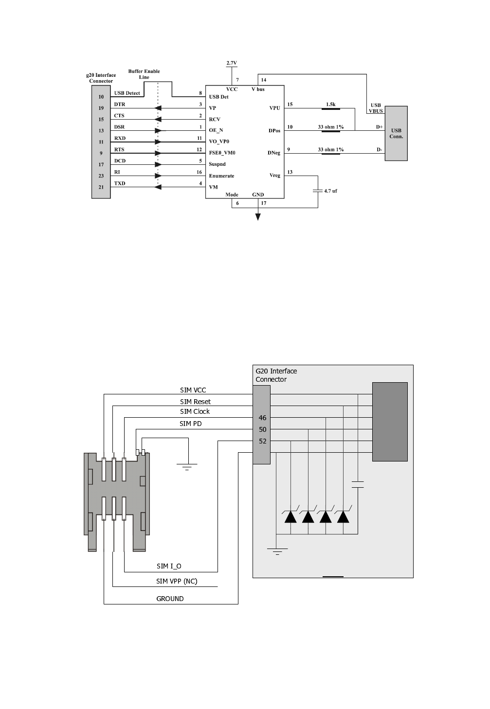
98-08901C64-O 21
Hardware Description
Figure 15 shows g20 USB connection for g20 models without a USB driver, using an external USB driver connection. The
circuit shown in this figure can be used by the user application in cases where a USB driver is needed.
Figure 15. g20 USB Connection for g20 Models without a USB Driver
3.3.3 SIM
The g20 includes a SIM card driver, however, it does not contain a SIM socket. SIM signals are routed to the interface connector
and include all the functionality required for SIM card operation.
3.3.3.1 SIM Connection
Figure 16 shows a g20 SIM connection:
Figure 16. g20 SIM Connection
48
44
1-4
SIM
Driver
6.8V Zeners
with low
Capacitance
For ESD protection
1uF
G20
DRAFT 1 (31.3.03)
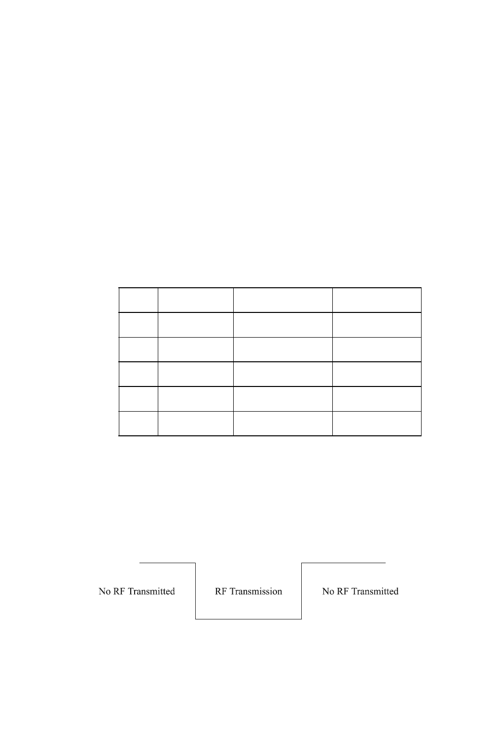
Hardware Description
22 98-08901C64-O
The following apply for g20 SIM connections:
•The g20 passes all SIM ETSI tests when an external socket is connected to the g20 with lines shorter than 10 cm.
•Longer connections require SIM testing to be performed in the user application.
•The g20 can work with 1.8 V or 3 V SIM cards.
•The g20 provides ESD protection for the SIM lines (6.8V Zener diodes with low capacitance), and for 1uF capacitors to the
SIM VCC.
•The SIM_PD (SIM Present Detect) signal is active when it is pulled low.
3.3.4 SPI
The SPI is a standard microprocessor bus used as a g20 debugging port. This port activates a debug option that enables logs to
be taken from the g20 while it is operating. It is recommended that this bus be accessible in the user application. In the g20
Developer’s Kit, the SPI is driven to an SPI/RS232 interface. The SPI is then converted and uses the RS232 port for debugging.
In the g20 Developer’s Kit, the SPI bus is converted to an RS232 protocol using a special interface circuit. It then uses the
standard RS232 port for debugging. Table 5 shows the pins available on the SPI bus.
3.3.4.1 SPI Connection
3.3.5 Unique g20 Interfaces
The g20 features certain unique functions (pins) that may be required by selected user applications, such as TX_EN, Antenna
Detect, GPRS Detect and Entertainment Mute. Each of these functions is described in the sections that follow.
3.3.5.1 Transmit Enable
This pin indicates when the g20 is transmitting RF in the antenna.
Figure 17. TX_EN Transmission
Table 5. SPI Pinout
Pin # Name Function Input/Output
70 SPI_CS SPI chip-select Output
62 SPI_IRQ SPI Interrupt Input
64 SPI_DIN SPI MISO input Input
68 SPI_DOUT SPI MOSI output Output
66 SPI_CLK SPI clock Output
DRAFT 1 (31.3.03)
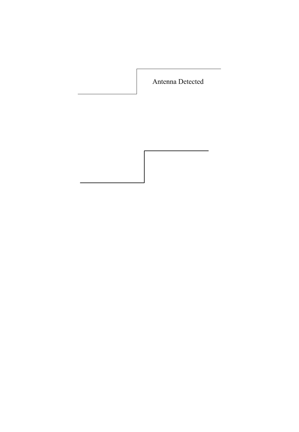
98-08901C64-O 23
Hardware Description
3.3.5.2 Antenna Detect
This pin indicates whether or not the antenna is inserted. This option was requested by a specific customer and was prepared
specifically for their board layout. Thus, this option is not supported by the basic g20 models.
The antenna-detect circuit detects whether the impedance of the antenna is 100 KΩ or lower. The antenna must have a resistance
to ground of less than 100 KΩ. in order to be detected.
Figure 18. Antenna-detect Circuit
3.3.5.3 GPRS-detect Coverage Indication
This pin indicates whether or not the g20 is located in an area with GPRS network coverage. This pin can be used to indicate
the GPRS coverage status before GPRS section activation has occurred, or before a switch to circuit-switched data is made.
Figure 19. GPRS-detect Coverage Indication
3.3.5.4 Entertainment Mute
This pin is reserved for future use. It will be dedicated to automotive applications in which there is a need to mute the entertain-
ment radio when there is a cellular call.
3.4 AUDIO INTERFACES
The g20 has an analog audio interface and a digital audio interface. Both of these interfaces are described in the sections that
follow.
3.4.1 Analog Audio Interfaces
The g20 supports microphone input, headset microphone input, differential speaker output, and a differential alert speaker.
3.4.1.1 Analog Input
The g20 has two analog inputs that are referenced to the microphone ground (pin 59):
•Headset microphone: Pin 57 is the headset microphone input. Input to this line can be directly from a headset microphone.
In order for the headset microphone to be active, the headset interrupt signal (pin 55) must be pulled low. The maximum
input to the g20 headset microphone before there is a distortion of the signal in the network is 12 mV RMS.
•Hands-free microphone: Pin 61 is the microphone input to the g20. The microphone is active when the headset interrupt
signal is not pulled low. The maximum input to the g20 microphone before there is a distortion of the signal in the network
is 32 mV RMS.
No GPRS Coverage GPRS Coverage
DRAFT 1 (31.3.03)
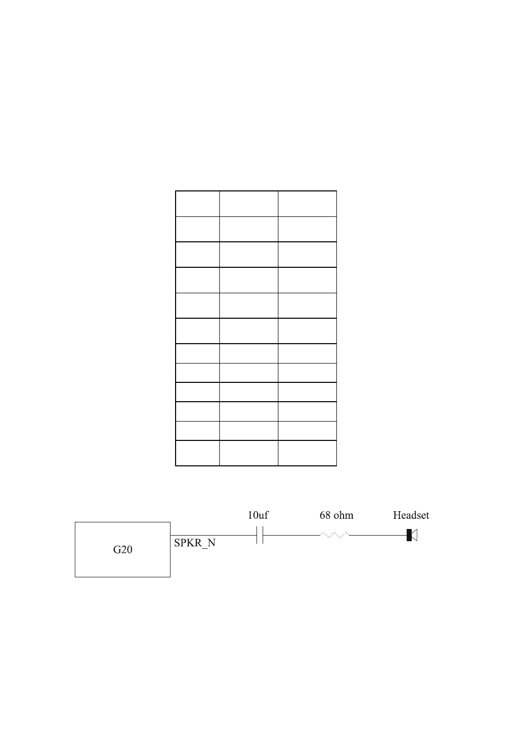
Hardware Description
24 98-08901C64-O
3.4.1.2 Analog Output
The g20 has a differential speaker output and an alert output:
•Speaker output: When headset mode is used, the headset speaker should be connected to the SPKR_N signal of the g20.
When a differential amplifier is used, both lines should be connected. An 8-ohm speaker can be connected directly to the
speaker lines.
•Alert: The g20 supports a direct connection for an alert transducer, in order to build a handset from the g20. All the sounds
that are transmitted to the alert can be routed to the speaker using the appropriate AT command.
Table 6 shows the SPKR_N output in headset mode for different network signal levels when the g20 is set to the maximum
volume level and the headset interrupt is pulled low.
The measurements shown in Table 6 apply in the following configuration:
Figure 20. SPKR_N Output Configuration
Table 6. SPKR_N Output when g20 Set to Maximum Volume Level and Headset Interrupt is Low
dBm0 mV RMS SPKR_N
3.14 1111.9 94
0 774.6 67
-5 435.6 38
-10 244.9 22
-15.5 130 12.5
-16 122.8 12
-17 109.4 11
-20 77.5 8.5
-25 43.6 6.5
-30 24.5 5.5
3000 250
DRAFT 1 (31.3.03)
98-08901C64-O 25
Hardware Description
Table 7 shows the output of the SPKR_N signal for different network signal levels when the g20 is set at the maximum volume
level and the headset interrupt is not pulled low.
Table 8 shows the SPKR_N output at different volume levels, when a 500mV RMS signal is transmitted from the network.
Table 7. SPKR_N Output when g20 Set to Maximum Volume Level and Headset Interrupt is Not Low
dBm0 mV RMS SPKR_N
3.14 1111.9 335
0 774.6 242
-5 435.6 134
-10 244.9 76
-15.5 130 41
-16 122.8 39
-17 109.4 34
-20 77.5 24
-25 43.6 14
-30 24.5 8
max 2900 900
Table 8. SPKR_N Output when a 500mV RMS Signal is Transmitted
Handset Volume SPKR_N
0 (lowest gain) 15
120
228
339
455
578
6110
7 (highest gain) 155
DRAFT 1 (31.3.03)
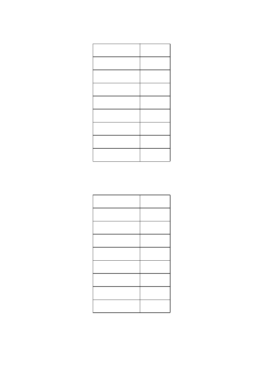
Hardware Description
26 98-08901C64-O
Table 9 shows the typical keypad tone levels generated by the g20. These measurements taken with the g20 in handset mode
(meaning the headset-detect signal is not pulled low).
Table 10 shows the keypad tone levels generated by the g20 when in headset mode (meaning the handset-detect signal is pulled
low).
Table 9. SPKR_N Output when g20 is in Handset Mode
Handset Volume SPKR_N
00
1122
2172
3244
4342
5482
6678
7954
Table 10. SPKR_N Output when g20 is in Headset Mode
Handset Volume SPKR_N
00
14
25.5
37.5
410.5
514
619.5
727.5
DRAFT 1 (31.3.03)
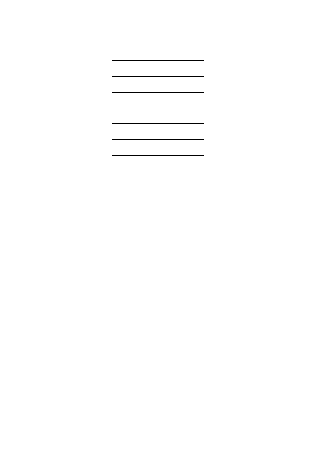
98-08901C64-O 27
Hardware Description
Table 11 shows the levels of the alert transducer measured on the ALERT_P signal at different ring volumes.
3.4.1.3 Audio Circuit Design Considerations
In order to design an audio circuit that produces clear audio, without being affected by the GSM transmission, the following
guidelines should be considered when designing the circuit:
•The audio input to the g20 should be referenced to the MIC_GND line of the g20.
•The microphone bias of the g20 for both the microphone and headset is 2.2 V. If a microphone with a different voltage is
used, the bias should be as clean as possible, and referenced to MIC_GND. Because most GSM buzz (217Hz TDMA noise)
is generated from the microphone path, if a different bias is created, it should be filtered to supply DC only.
•The MIC_GND and GND are connected inside the g20 and should not be connected to the application board.
•Keep the lines of the microphone inputs as short as possible. To filter the lines from RF emission, 39pF capacitors can be
used.
•The g20 GND should be connected on all four pins, with two mounting screws to the application ground.
•If possible, the RF cable ground from the g20 should be connected to the GND of the g20.
•The digital lines of the application should never be referenced to the MIC_GND.
3.4.2 Digital Audio Interface
The g20 digital audio interface is a full-duplex SAP (serial audio port) comprised of four signals:
•PCM_FS: This pin is used for frame sync output provided by the g20.
•PCM_CLK: This pin is used for the clock output provided by the g20.
•PCM_DIN: This pin is the serial input to the g20 SAP.
•PCM_DOUT: This pin is the serial output of the g20 SAP.
The following conditions apply to the digital audio interface of the g20:
•The g20 SAP works in network mode, with four slots in each frame. Each slot consists of 16-bit data.
•The frame sync rate is 8 KHz, and the clock rate is 512 KHz.
•The g20 is the master in the SAP network. Therefore, the connected DSP should be configured as the host.
Table 11. Alert Transducer Levels for the ALERT_P Signal
Handset Volume ALRT_P
0107
1153
2206
3305
4424
5600
6850
71200
DRAFT 1 (31.3.03)
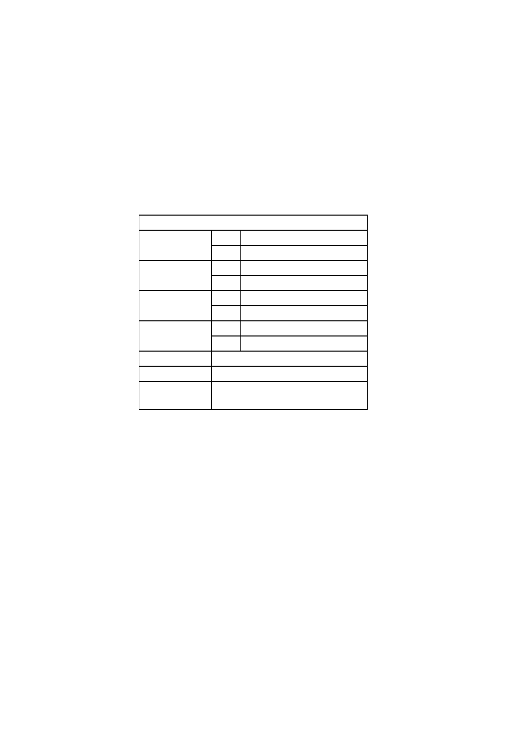
Hardware Description
28 98-08901C64-O
3.5 ANTENNA
The g20 has two models, one for North America Frequency bands (850/1900 MHz), and one for European Bands
(900/1800 MHz). The following connection requirements apply for the g20 antenna:
•The g20 is terminated with an MMCX connector, and with 50-ohm impedance in the relevant frequencies.
•The g20 can be connected to any antenna with 50-ohm impedance in the relevant frequency bands.
•The g20 is designed to work on VSWR, up to 3:1 The antenna should meet this requirement.
3.5.1 Antenna Performance Recommendations
Table 12 lists the performance recommendations for the g20 antenna.
3.6 CHARGER INTERFACE
g20 software supports charging circuitry for 3.6 V Lithium Ion batteries on some g20 models. The software interface is designed
to work with a charging IC from National Semiconductor, model LM3652. Refer to the schematics chapter in the g20
Developer’s Kit for more details about the design of the charging circuitry.
3.7 DISPLAY INTERFACE
The g20 supports a four-level gray-scale display with 96 x 65 pixels. The following five lines should be connected to the display:
•LCD_CS
•LCD_RS
•LCD_DATA
•LCD_CLK
•RESET_N
Use the BL_SINK line for backlighting (display and keypad) when using the display. The backlight sink can provide current up
to 100 mA, and can be used as an open drain output for more than 100 mA.
Table 12. Antenna Performance Recommendations
Frequencies:
GSM 850 TX 824 – 849 MHz
RX 869 – 893 MHz
GSM 900 TX 880 – 915 MHz
RX 925 – 960 MHz
DCS 1800 TX 1710 – 1785 MHz
RX 1805 – 1880 MHz
PCS 1900 TX 1850 - 1910 MHz
RX 1930 – 1990 MHz
Gain: 0 dBi (unity) gain or greater
Impedance: 50 Ohm
VSWR: Typical: 1.5:1
Worst case: 2.5:1
DRAFT 1 (31.3.03)

98-08901C64-O 29
Hardware Description
3.8 ESD PROTECTION
In general, the g20 does not include embedded ESD protection circuits. This type of protection should be implemented in the
customer application. Partial ESD protection is provided, as follows:
•SIM lines are protected up to 3 KV with 6.8 V Zener Diodes.
•VCC input is protected with a 2.2 uF capacitor.
•Ignition input is protected with a 100 nF capacitor.
DRAFT 1 (31.3.03)

Hardware Description
30 98-08901C64-O
DRAFT 1 (31.3.03)
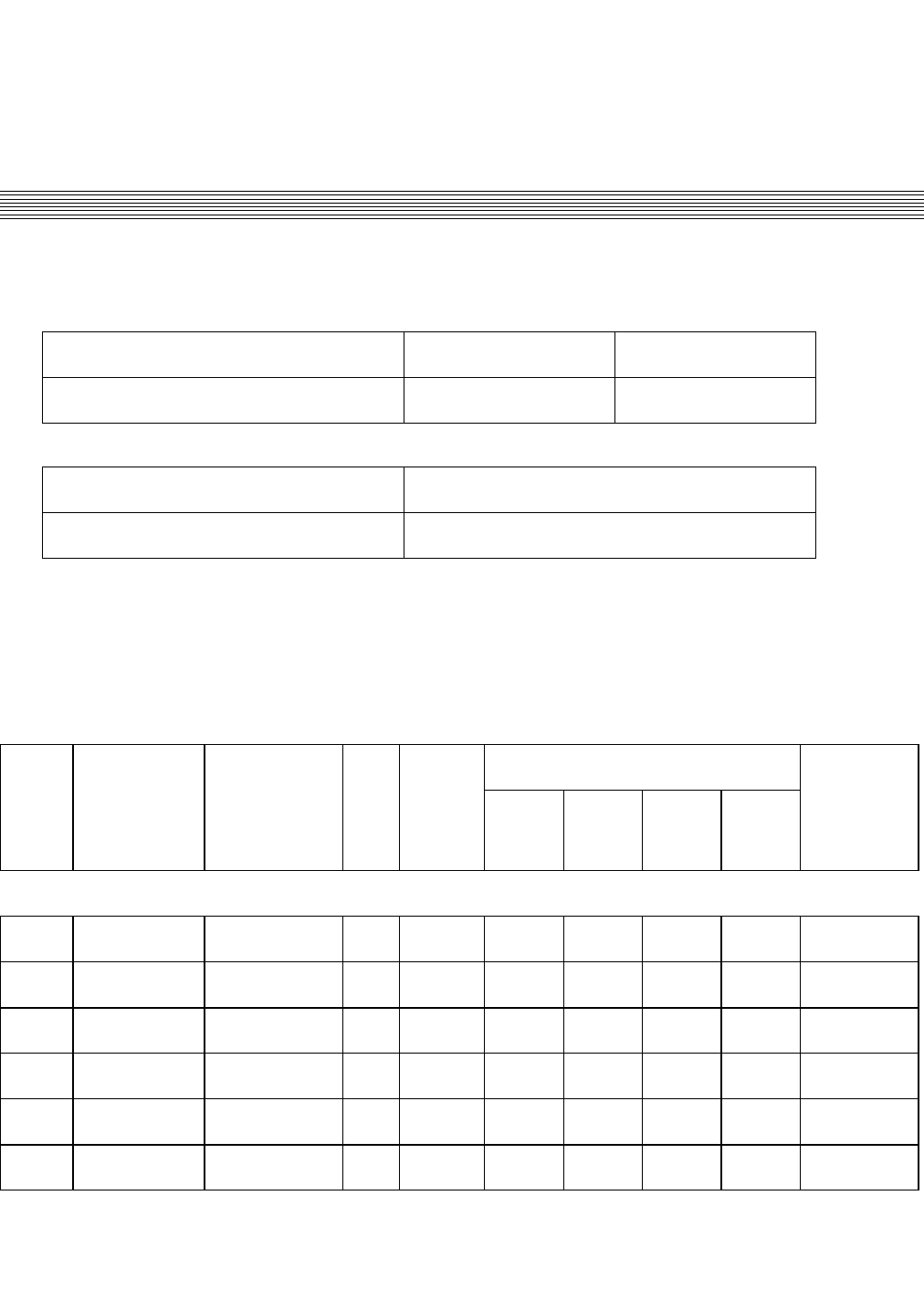
98-08901C64-O 31
4. CONNECTOR PIN
ASSIGNMENTS
4.1 CONNECTORS
The g20 has two connectors: the g20 interface connector and the g20 RF connector. Each is described below.
4.2 PIN ASSIGNMENTS
The g20 interface is provided via a 70-pin connector. Table 13 describes the pin assignments for the g20 interface connector.
g20 Interface Connector Mating Connector Stacking Height
70-pin, 0.5mm pitch, Molex 53748-0708 Molex 52991-0708 3.0 mm
g20 RF Connector Mating Connector
Standard MMCX female Standard MMCX male (connector for cable)
Table 13. g20 Interface Connector Pin Assignments
Pin # Signal Name Description I/O Signal
Level Models
with USB
Driver/
Alternate
Function
Min Typ Max Units
Power:
1 GND Ground GND
2 GND Ground GND
3 GND Ground GND
4 GND Ground GND
5 VCC Power supply I DC 3.0 3.6 4.2 V
6 VCC Power supply I DC 3.0 3.6 4.2 V
DRAFT 1 (31.3.03)
Connector Pin Assignments
32 98-08901C64-O
7 VCC Power supply I DC 3.0 3.6 4.2 V
8 VCC Power supply I DC 3.0 3.6 4.2 V
GPIO:
16 WAKEUP_IN Wakeup input I Logic 2.775 V
26 WAKEUP_
OUT Wakeup
output O Logic 2.775 V
25 RESET Reset signal
output O Logic 2.775 V
53 ON_OFF On/off switch I DC 3.0 3.6 4.2 V
51 IGN Ignition input I Logic 2.775 3.6 16 V
39 TX_EN GSM transmit
indicator O Logic 2.775 V
41 ANT_DET Antenna-
presence
detect O Logic 2.775 V
49 GPRS_DET GPRS
coverage
indicator O Logic 2.775 V
37 ENT_MUTE Entertainment
mute O Logic 2.775 V
UART:
21 TXD RS232 TXD I Logic 2.775 V USB VMIN
11 RXD RS232 RXD O Logic 2.775 V USB
VPOUT
9 RTS RS232 RTS I Logic 2.775 V USB XRXD
15 CTS RS232 CTS O Logic 2.775 V USB
VMOUT
19 DTR RS232 DTR I Logic 2.775 V USB VPIN
Table 13. g20 Interface Connector Pin Assignments (Continued)
Pin # Signal Name Description I/O Signal
Level Models
with USB
Driver/
Alternate
Function
Min Typ Max Units
DRAFT 1 (31.3.03)
98-08901C64-O 33
Connector Pin Assignments
13 DSR RS232 DSR O Logic 2.775 V USB
TXENB
17 DCD RS232 DCD O Logic 2.775 V USB
SUSPEND
23 RI RS232 RI O Logic 2.775 V USB
SOFTCON
USB:
10 USB_DET USB-
connection
detect I DC 4.4 5 5.25 V USB_
VBUS
12 Not
connected USB_D+
14 Not
connected USB_D-
SPI:
70 SPI_CS SPI chip-
select O Logic 2.775 V
62 SPI_IRQ SPI interrupt I Logic 2.775 V
64 SPI_DIN SPI MISO
input I Logic 2.775 V
68 SPI_DOUT SPI MOSI
output O Logic 2.775 V
66 SPI_CLK SPI clock O Logic 2.775 V
SIM Card:
50 SIM_PD SIM-
presence
detect I Logic 2.775 V
48 SIM_VCC SIM VCC O DC 1.8 3 V
44 SIM_RST SIM reset O Logic 1.8 3 V
Table 13. g20 Interface Connector Pin Assignments (Continued)
Pin # Signal Name Description I/O Signal
Level Models
with USB
Driver/
Alternate
Function
Min Typ Max Units
DRAFT 1 (31.3.03)
Connector Pin Assignments
34 98-08901C64-O
52 SIM_DIO SIM serial
data I/O Logic 1.8 3 V
46 SIM_CLK SIM clock O Logic 1.8 3 V
PCM Audio:
18 PCM_DIN Digital audio
receive I Logic 2.775 V
20 PCM_DOUT Digital audio
transmit O Logic 2.775 V
22 PCM_CLK Digital audio
clock O Logic 2.775 V
24 PCM_FS Digital audio
frame sync O Logic 2.775 V
Display:
54 LCD_CS Display chip-
select O Logic 2.775 V
60 LCD_RS Display
register-select O Logic 2.775 V
56 LCD_DATA Display serial
data O Logic 2.775 V
58 LCD_CLK Display serial
clock O Logic 2.775 V
Keypad:
30 KBC0 Keypad
column 0 I Logic 2.775 V
28 KBC1 Keypad
column 1 I Logic 2.775 V
32 KBR0 Keypad row 0 I Logic 2.775 V
34 KBR1 Keypad row 1 I Logic 2.775 V
36 KBR2 Keypad row 2 I Logic 2.775 V
Table 13. g20 Interface Connector Pin Assignments (Continued)
Pin # Signal Name Description I/O Signal
Level Models
with USB
Driver/
Alternate
Function
Min Typ Max Units
DRAFT 1 (31.3.03)
98-08901C64-O 35
Connector Pin Assignments
38 KBR3 Keypad row 3 I Logic 2.775 V
40 KBR4 Keypad row 4 I Logic 2.775 V
42 KBR5 Keypad row 5 I Logic 2.775 V
Audio:
67 SPKR_N Speaker
inverted OAudio V
69 SPKR_P Speaker O Audio V
63 ALRT_N Alert speaker
inverted OLogic V
65 ALRT_P Alert speaker O Audio V
61 MIC Microphone
input IAudio V
59 MIC_GND
Microphone
ground What
goes in I/O
column for
this pin?
GND V
57 HDST_MIC Headset
microphone IAudio V
55 HDST_INT Headset-
detect
interrupt I Logic 2.775 V
Charger:
35 CHRG_DET Charger-
presence
detect I Logic 2.775 V
33 CHRG_
STATE Charger rate
indicator I Logic 2.775 V
31 CHRG_SW Accessory
current control O Logic 2.775 V
Table 13. g20 Interface Connector Pin Assignments (Continued)
Pin # Signal Name Description I/O Signal
Level Models
with USB
Driver/
Alternate
Function
Min Typ Max Units
DRAFT 1 (31.3.03)
Connector Pin Assignments
36 98-08901C64-O
29 CHRG_DIS Charger
disable O Logic 2.775 V
ADC:
45 CHRG_TYP Accessory-
type detect I Logic 0 2.775 V
47 THERM Temperature
measurement I Logic 0 2.775 V
Miscellaneous:
27 BL_SINK Backlight
current sink IDC 80100mA
43 VIB_OUT Vibrator
regulator ODC 1.3 V
Table 13. g20 Interface Connector Pin Assignments (Continued)
Pin # Signal Name Description I/O Signal
Level Models
with USB
Driver/
Alternate
Function
Min Typ Max Units
DRAFT 1 (31.3.03)
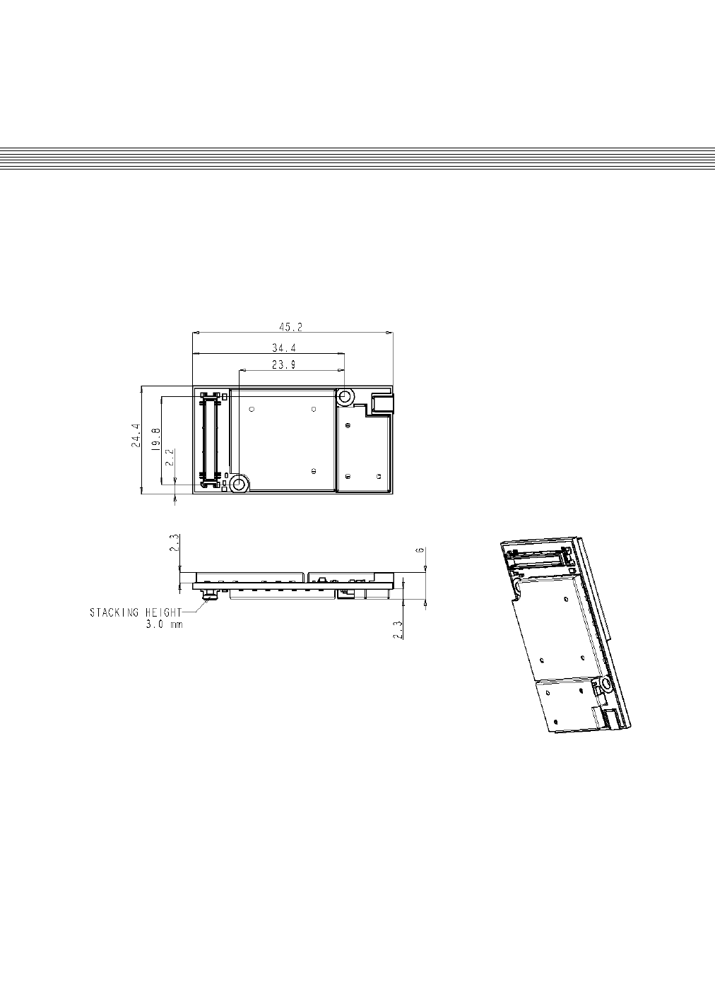
98-08901C64-O 37
5. MECHANICAL DESCRIPTION
5.1 MECHANICAL DETAILS
This section describes the mechanical details for the g20:
Size: 45.2x24.4x6 mm
Mounting: Two 2.4 mmØ holes are provided that accommodate M2 screws or #1-64 UNC 2A machine screws. Torque to
2 inches per pound. Refer to Figure 21 below for mounting requirements.
Figure 21. Mechanical Mounting Requirements
DRAFT 1 (31.3.03)

Mechanical Description
38 98-08901C64-O
DRAFT 1 (31.3.03)

98-08901C64-O 39
6. SERVICE SUPPORT
6.1 CUSTOMER ASSISTANCE
For customer assistance, contact us as directed below:
Helpdesk email: n2cshd@motorola.com
Helpdesk telephone: +972-3-568-4040
6.2 TESTING A STANDALONE UNIT
PLEASE PROVIDE DETAILS FOR THIS SECTION.
6.3 TROUBLESHOOTING
PLEASE PROVIDE DETAILS FOR THIS SECTION.
6.4 PROGRAMMING
PLEASE PROVIDE DETAILS FOR THIS SECTION.
DRAFT 1 (31.3.03)

Service Support
40 98-08901C64-O
DRAFT 1 (31.3.03)

98-08901C64-O 41
7. INDEX
DRAFT 1 (31.3.03)

Index
42 98-08901C64-O
DRAFT 1 (31.3.03)