Motorola Coldfire Mcf5281 Users Manual 5282UM
MCF5282 to the manual e9f134fe-e16d-4974-b62a-d3be4b7a3ce2
2015-01-23
: Motorola Motorola-Coldfire-Mcf5281-Users-Manual-271786 motorola-coldfire-mcf5281-users-manual-271786 motorola pdf
Open the PDF directly: View PDF ![]() .
.
Page Count: 816 [warning: Documents this large are best viewed by clicking the View PDF Link!]
- About This Book
- Chapter 1 Overview
- 1.1 MCF5282 Key Features
- Figure 1-1. MCF5282 Block Diagram
- 1.1.1 Version 2 ColdFire Core
- 1.1.2 System Control Module
- 1.1.3 External Interface Module (EIM)
- 1.1.4 Chip Select
- 1.1.5 Power Management
- 1.1.6 General Input/Output Ports
- 1.1.7 Interrupt Controllers (INTC0/INTC1)
- 1.1.8 SDRAM Controller
- 1.1.9 Test Access Port
- 1.1.10 UART Modules
- 1.1.11 DMA Timers (DTIM0-DTIM3)
- 1.1.12 General-Purpose Timers (GPTA/GPTB)
- 1.1.13 Periodic Interrupt Timers (PIT0-PIT3)
- 1.1.14 Software Watchdog Timer
- 1.1.15 Phase Locked Loop (PLL)
- 1.1.16 DMA Controller
- 1.1.17 Reset
- 1.2 MCF5282-Specific Features
- 1.1 MCF5282 Key Features
- Chapter 2 ColdFire Core
- 2.1 Processor Pipelines
- 2.2 Processor Register Description
- 2.2.1 User Programming Model
- 2.2.2 EMAC Programming Model
- 2.2.3 Supervisor Programming Model
- 2.3 Programming Model
- 2.4 Additions to the Instruction Set Architecture
- 2.5 Exception Processing Overview
- 2.6 Exception Stack Frame Definition
- 2.7 Processor Exceptions
- 2.7.1 Access Error Exception
- 2.7.2 Address Error Exception
- 2.7.3 Illegal Instruction Exception
- 2.7.4 Divide-By-Zero
- 2.7.5 Privilege Violation
- 2.7.6 Trace Exception
- 2.7.7 Unimplemented Line-A Opcode
- 2.7.8 Unimplemented Line-F Opcode
- 2.7.9 Debug Interrupt
- 2.7.10 RTE and Format Error Exception
- 2.7.11 TRAP Instruction Exception
- 2.7.12 Interrupt Exception
- 2.7.13 Fault-on-Fault Halt
- 2.7.14 Reset Exception
- 2.8 Instruction Execution Timing
- 2.9 Standard One Operand Instruction Execution Times
- 2.10 Standard Two Operand Instruction Execution Times
- 2.11 Miscellaneous Instruction Execution Times
- 2.12 EMAC Instruction Execution Times
- 2.13 Branch Instruction Execution Times
- 2.14 ColdFire Instruction Set Architecture Enhancements
- Chapter 3 Enhanced Multiply-Accumulate Unit (EMAC)
- Chapter 4 Cache
- Chapter 5 Static RAM (SRAM)
- Chapter 6 ColdFire Flash Module (CFM)
- 6.1 Features
- 6.2 Block Diagram
- 6.3 Memory Map
- Figure 6-2. CFM Array Memory Map
- 6.3.1 CFM Configuration Field
- 6.3.2 Flash Base Address Register (FLASHBAR)
- 6.3.3 CFM Registers
- 6.3.4 Register Descriptions
- 6.3.4.1 CFM Configuration Register (CFMCR)
- 6.3.4.2 CFM Clock Divider Register (CFMCLKD)
- 6.3.4.3 CFM Security Register (CFMSEC)
- 6.3.4.4 CFM Protection Register (CFMPROT)
- 6.3.4.5 CFM Supervisor Access Register (CFMSACC)
- 6.3.4.6 CFM Data Access Register (CFMDACC)
- 6.3.4.7 CFM User Status Register (CFMUSTAT)
- 6.3.4.8 CFM Command Register (CFMCMD)
- 6.4 CFM Operation
- 6.5 Flash Security Operation
- 6.6 Reset
- 6.7 Interrupts
- Chapter 7 Power Management
- 7.1 Features
- 7.2 Memory Map and Registers
- 7.3 Functional Description
- 7.3.1 Low-Power Modes
- 7.3.2 Peripheral Behavior in Low-Power Modes
- 7.3.2.1 ColdFire Core
- 7.3.2.2 Static Random-Access Memory (SRAM)
- 7.3.2.3 Flash
- 7.3.2.4 System Control Module (SCM)
- 7.3.2.5 SDRAM Controller (SDRAMC)
- 7.3.2.6 Chip Select Module
- 7.3.2.7 DMA Controller (DMAC0-DMA3)
- 7.3.2.8 UART Modules (UART0, UART1, and UART2)
- 7.3.2.9 I2C Module
- 7.3.2.10 Queued Serial Peripheral Interface (QSPI)
- 7.3.2.11 DMA Timers (DMAT0-DMAT3)
- 7.3.2.12 Interrupt Controllers (INTC0, INTC1)
- 7.3.2.13 Fast Ethernet Controller (FEC)
- 7.3.2.14 I/O Ports
- 7.3.2.15 Reset Controller
- 7.3.2.16 Chip Configuration Module
- 7.3.2.17 Clock Module
- 7.3.2.18 Edge Port
- 7.3.2.19 Watchdog Timer
- 7.3.2.20 Programmable Interrupt Timers (PIT0, PIT1, PIT2 and PIT3)
- 7.3.2.21 Queued Analog-to-Digital Converter (QADC)
- 7.3.2.22 General Purpose Timers (GPTA and GPTB)
- 7.3.2.23 FlexCAN
- 7.3.2.24 ColdFire Flash Module
- 7.3.2.25 BDM
- 7.3.2.26 JTAG
- 7.3.3 Summary of Peripheral State During Low-Power Modes
- Chapter 8 System Control Module (SCM)
- 8.1 Overview
- 8.2 Features
- 8.3 Memory Map and Register Definition
- 8.4 Register Descriptions
- 8.5 Internal Bus Arbitration
- 8.6 System Access Control Unit (SACU)
- Chapter 9 Clock Module
- 9.1 Features
- 9.2 Modes of Operation
- 9.3 Low-power Mode Operation
- 9.4 Block Diagram
- 9.5 Signal Descriptions
- 9.6 Memory Map and Registers
- 9.7 Functional Description
- 9.7.1 System Clock Modes
- 9.7.2 Clock Operation During Reset
- 9.7.3 System Clock Generation
- 9.7.4 PLL Operation
- Figure 9-5. Crystal Oscillator Example
- 9.7.4.1 Phase and Frequency Detector (PFD)
- 9.7.4.2 Charge Pump/Loop Filter
- 9.7.4.3 Voltage Control Output (VCO)
- 9.7.4.4 Multiplication Factor Divider (MFD)
- 9.7.4.5 PLL Lock Detection
- 9.7.4.6 PLL Loss of Lock Conditions
- 9.7.4.7 PLL Loss of Lock Reset
- 9.7.4.8 Loss of Clock Detection
- 9.7.4.9 Loss of Clock Reset
- 9.7.4.10 Alternate Clock Selection
- 9.7.4.11 Loss of Clock in Stop Mode
- Chapter 10 Interrupt Controller Modules
- 10.1 68K/ColdFire Interrupt Architecture Overview
- 10.2 Memory Map
- 10.3 Register Descriptions
- 10.3.1 Interrupt Pending Registers (IPRHn, IPRLn)
- 10.3.2 Interrupt Mask Register (IMRHn, IMRLn)
- 10.3.3 Interrupt Force Registers (INTFRCHn, INTFRCLn)
- 10.3.4 Interrupt Request Level Register (IRLRn)
- 10.3.5 Interrupt Acknowledge Level and Priority Register (IACKLPRn)
- 10.3.6 Interrupt Control Register (ICRnx, (x = 1, 2,..., 63))
- 10.3.7 Software and Level n IACK Registers (SWIACKR, L1IACK-L7IACK)
- 10.4 Prioritization Between Interrupt Controllers
- 10.5 Low-Power Wakeup Operation
- Chapter 11 Edge Port Module (EPORT)
- 11.1 Introduction
- 11.2 Low-Power Mode Operation
- 11.3 Interrupt/General-Purpose I/O Pin Descriptions
- 11.4 Memory Map and Registers
- Chapter 12 Chip Select Module
- 12.1 Overview
- 12.2 Chip Select Module Signals
- 12.3 Chip Select Operation
- 12.4 Chip Select Registers
- Chapter 13 External Interface Module (EIM)
- 13.1 Features
- 13.2 Bus and Control Signals
- 13.3 Bus Characteristics
- 13.4 Data Transfer Operation
- Figure 13-2. Connections for External Memory Port Sizes
- Figure 13-3. Chip-Select Module Output Timing Diagram
- 13.4.1 Bus Cycle Execution
- 13.4.2 Data Transfer Cycle States
- 13.4.3 Read Cycle
- 13.4.4 Write Cycle
- 13.4.5 Fast Termination Cycles
- 13.4.6 Back-to-Back Bus Cycles
- 13.4.7 Burst Cycles
- 13.5 Misaligned Operands
- Chapter 14 Signal Descriptions
- 14.1 Overview
- 14.2 MCF5282 External Signals
- 14.2.1 External Interface Module (EIM) Signals
- 14.2.1.1 Address Bus (A[23:0])
- 14.2.1.2 Data Bus (D[31:0])
- 14.2.1.3 Byte Strobes (BS[3:0])
- 14.2.1.4 Output Enable (OE)
- 14.2.1.5 Transfer Acknowledge (TA)
- 14.2.1.6 Transfer Error Acknowledge (TEA)
- 14.2.1.7 Read/Write (R/W)
- 14.2.1.8 Transfer Size(SIZ[1:0])
- 14.2.1.9 Transfer Start (TS)
- 14.2.1.10 Transfer In Progress (TIP)
- 14.2.1.11 Chip Selects (CS[6:0])
- 14.2.2 SDRAM Controller Signals
- 14.2.3 Clock and Reset Signals
- 14.2.4 Chip Configuration Signals
- 14.2.5 External Interrupt Signals
- 14.2.6 Ethernet Module Signals
- 14.2.6.1 Management Data (EMDIO)
- 14.2.6.2 Management Data Clock (EMDC)
- 14.2.6.3 Transmit Clock (ETXCLK)
- 14.2.6.4 Transmit Enable (ETXEN)
- 14.2.6.5 Transmit Data 0 (ETXD0)
- 14.2.6.6 Collision (ECOL)
- 14.2.6.7 Receive Clock (ERXCLK)
- 14.2.6.8 Receive Data Valid (ERXDV)
- 14.2.6.9 Receive Data 0 (ERXD0)
- 14.2.6.10 Carrier Receive Sense (ECRS)
- 14.2.6.11 Transmit Data 1-3 (ETXD[3:1])
- 14.2.6.12 Transmit Error (ETXER)
- 14.2.6.13 Receive Data 1-3 (ERXD[3:1])
- 14.2.6.14 Receive Error (ERXER)
- 14.2.7 Queued Serial Peripheral Interface (QSPI) Signals
- 14.2.8 FlexCAN Signals
- 14.2.9 I2C Signals
- 14.2.10 UART Module Signals
- 14.2.11 General Purpose Timer Signals
- 14.2.12 DMA Timer Signals
- 14.2.13 Analog-to-Digital Converter Signals
- 14.2.13.1 QADC Analog Input (AN0/ANW)
- 14.2.13.2 QADC Analog Input (AN1/ANX)
- 14.2.13.3 QADC Analog Input (AN2/ANY)
- 14.2.13.4 QADC Analog Input (AN3/ANZ)
- 14.2.13.5 QADC Analog Input (AN52/MA0)
- 14.2.13.6 QADC Analog Input (AN53/MA1)
- 14.2.13.7 QADC Analog Input (AN55/TRIG1)
- 14.2.13.8 QADC Analog Input (AN56/TRIG2)
- 14.2.14 Debug Support Signals
- 14.2.14.1 JTAG_EN
- 14.2.14.2 Development Serial Clock/Test Reset (DSCLK/TRST)
- 14.2.14.3 Breakpoint/Test Mode Select (BKPT/TMS)
- 14.2.14.4 Development Serial Input/Test Data (DSI/TDI)
- 14.2.14.5 Development Serial Output/Test Data (DSO/TDO)
- 14.2.14.6 Test Clock (TCLK)
- 14.2.14.7 Debug Data (DDATA[3:0])
- 14.2.14.8 Processor Status Outputs (PST[3:0])
- 14.2.15 Test Signals
- 14.2.16 Power and Reference Signals
- 14.2.16.1 QADC Analog Reference (VRH, VRL)
- 14.2.16.2 QADC Analog Supply (VDDA, VSSA)
- 14.2.16.3 PLL Analog Supply (VDDPLL, VSSPLL)
- 14.2.16.4 QADC Positive Supply (VDDH)
- 14.2.16.5 Power for Flash Erase/Program (VPP)
- 14.2.16.6 Power and Ground for Flash Array (VDDF, VSSF)
- 14.2.16.7 Standby Power (VSTBY)
- 14.2.16.8 Positive Supply (VDD)
- 14.2.16.9 Ground (VSS)
- 14.2.1 External Interface Module (EIM) Signals
- Chapter 15 Synchronous DRAM Controller Module
- 15.1 Overview
- 15.2 SDRAM Controller Operation
- Table 15-1. SDRAM Commands
- 15.2.1 DRAM Controller Signals
- 15.2.2 Memory Map for SDRAMC Registers
- 15.2.3 General Synchronous Operation Guidelines
- 15.2.3.1 Address Multiplexing
- Table 15-7. Generic Address Multiplexing Scheme
- Table 15-8. MCF5282 to SDRAM Interface (8-Bit Port, 9-Column Address Lines)
- Table 15-9. MCF5282 to SDRAM Interface (8-Bit Port,10-Column Address Lines)
- Table 15-10. MCF5282 to SDRAM Interface (8-Bit Port,11-Column Address Lines)
- Table 15-11. MCF5282 to SDRAM Interface (8-Bit Port,12-Column Address Lines)
- Table 15-12. MCF5282 to SDRAM Interface (8-Bit Port,13-Column Address Lines)
- Table 15-13. MCF5282 to SDRAM Interface (16-Bit Port, 8-Column Address Lines)
- Table 15-14. MCF5282 to SDRAM Interface (16-Bit Port, 9-Column Address Lines)
- Table 15-15. MCF5282 to SDRAM Interface (16-Bit Port, 10-Column Address Lines)
- Table 15-16. MCF5282 to SDRAM Interface (16-Bit Port, 11-Column Address Lines)
- Table 15-17. MCF5282 to SDRAM Interface (16-Bit Port, 12-Column Address Lines)
- Table 15-18. MCF5282 to SDRAM Interface (16-Bit Port, 13-Column-Address Lines)
- Table 15-19. MCF5282 to SDRAM Interface (32-Bit Port, 8-Column Address Lines)
- Table 15-20. MCF5282 to SDRAM Interface (32-Bit Port, 9-Column Address Lines)
- Table 15-21. MCF5282 to SDRAM Interface (32-Bit Port, 10-Column Address Lines)
- Table 15-22. MCF5282 to SDRAM Interface (32-Bit Port, 11-Column Address Lines)
- Table 15-23. MCF5282 to SDRAM Interface (32-Bit Port, 12-Column Address Lines)
- 15.2.3.2 SDRAM Byte Strobe Connections
- 15.2.3.3 Interfacing Example
- 15.2.3.4 Burst Page Mode
- 15.2.3.5 Auto-Refresh Operation
- 15.2.3.6 Self-Refresh Operation
- 15.2.3.1 Address Multiplexing
- 15.2.4 Initialization Sequence
- 15.3 SDRAM Example
- Chapter 16 DMA Controller Module
- 16.1 Overview
- 16.2 DMA Request Control (DMAREQC)
- 16.3 DMA Transfer Overview
- 16.4 DMA Controller Module Programming Model
- 16.5 DMA Controller Module Functional Description
- Chapter 17 Fast Ethernet Controller (FEC)
- 17.1 Overview
- 17.2 Modes of Operation
- 17.3 FEC Top-Level Functional Diagram
- 17.4 Functional Description
- 17.4.1 Initialization Sequence
- 17.4.2 User Initialization (Prior to Asserting ECR[ETHER_EN])
- 17.4.3 Microcontroller Initialization
- 17.4.4 User Initialization (After Asserting ECR[ETHER_EN])
- 17.4.5 Network Interface Options
- 17.4.6 FEC Frame Transmission
- 17.4.7 FEC Frame Reception
- 17.4.8 Ethernet Address Recognition
- 17.4.9 Hash Algorithm
- 17.4.10 Full Duplex Flow Control
- 17.4.11 Inter-Packet Gap (IPG) Time
- 17.4.12 Collision Handling
- 17.4.13 Internal and External Loopback
- 17.4.14 Ethernet Error-Handling Procedure
- 17.5 Programming Model
- 17.5.1 Top Level Module Memory Map
- 17.5.2 Detailed Memory Map (Control/Status Registers)
- 17.5.3 MIB Block Counters Memory Map
- 17.5.4 Registers
- 17.5.4.1 Ethernet Interrupt Event Register (EIR)
- 17.5.4.2 Interrupt Mask Register (EIMR)
- 17.5.4.3 Receive Descriptor Active Register (RDAR)
- 17.5.4.4 Transmit Descriptor Active Register (TDAR)
- 17.5.4.5 Ethernet Control Register (ECR)
- 17.5.4.6 MII Management Frame Register (MMFR)
- 17.5.4.7 MII Speed Control Register (MSCR)
- 17.5.4.8 MIB Control Register (MIBC)
- 17.5.4.9 Receive Control Register (RCR)
- 17.5.4.10 Transmit Control Register (TCR)
- 17.5.4.11 Physical Address Low Register (PALR)
- 17.5.4.12 Physical Address High Register (PAUR)
- 17.5.4.13 Opcode/Pause Duration Register (OPD)
- 17.5.4.14 Descriptor Individual Upper Address Register (IAUR)
- 17.5.4.15 Descriptor Individual Lower Address (IALR)
- 17.5.4.16 Descriptor Group Upper Address (GAUR)
- 17.5.4.17 Descriptor Group Lower Address (GALR)
- 17.5.4.18 FIFO Transmit FIFO Watermark Register (TFWR)
- 17.5.4.19 FIFO Receive Bound Register (FRBR)
- 17.5.4.20 FIFO Receive Start Register (FRSR)
- 17.5.4.21 Receive Descriptor Ring Start (ERDSR)
- 17.5.4.22 Transmit Buffer Descriptor Ring Start (ETSDR)
- 17.5.4.23 Receive Buffer Size Register (EMRBR)
- 17.6 Buffer Descriptors
- Chapter 18 Watchdog Timer Module
- Chapter 19 Programmable Interrupt Timer Modules (PIT0-PIT3)
- Chapter 20 General Purpose Timer Modules (GPTA and GPTB)
- 20.1 Features
- 20.2 Block Diagram
- 20.3 Low-Power Mode Operation
- 20.4 Signal Description
- 20.5 Memory Map and Registers
- Table 20-3. GPT Modules Memory Map (continued)
- 20.5.1 GPT Input Capture/Output Compare Select Register (GPTIOS)
- 20.5.2 GPT Compare Force Register (GPCFORC)
- 20.5.3 GPT Output Compare 3 Mask Register (GPTOC3M)
- 20.5.4 GPT Output Compare 3 Data Register (GPTOC3D)
- 20.5.5 GPT Counter Register (GPTCNT)
- 20.5.6 GPT System Control Register 1 (GPTSCR1)
- 20.5.7 GPT Toggle-On-Overflow Register (GPTTOV)
- 20.5.8 GPT Control Register 1 (GPTCTL1)
- 20.5.9 GPT Control Register 2 (GPTCTL2)
- 20.5.10 GPT Interrupt Enable Register (GPTIE)
- 20.5.11 GPT System Control Register 2 (GPTSCR2)
- 20.5.12 GPT Flag Register 1 (GPTFLG1)
- 20.5.13 GPT Flag Register 2 (GPTFLG2)
- 20.5.14 GPT Channel Registers (GPTCn)
- 20.5.15 Pulse Accumulator Control Register (GPTPACTL)
- 20.5.16 Pulse Accumulator Flag Register (GPTPAFLG)
- 20.5.17 Pulse Accumulator Counter Register (GPTPACNT)
- 20.5.18 GPT Port Data Register (GPTPORT)
- 20.5.19 GPT Port Data Direction Register (GPTDDR)
- 20.6 Functional Description
- 20.7 Reset
- 20.8 Interrupts
- Chapter 21 DMA Timers (DTIM0-DTIM3)
- 21.1 Overview
- 21.2 DMA Timer Programming Model
- 21.2.1 Prescaler
- 21.2.2 Capture Mode
- 21.2.3 Reference Compare
- 21.2.4 Output Mode
- 21.2.5 Memory Map
- 21.2.6 DMA Timer Mode Registers (DTMRn)
- 21.2.7 DMA Timer Extended Mode Registers (DTXMRn)
- 21.2.8 DMA Timer Event Registers (DTERn)
- 21.2.9 DMA Timer Reference Registers (DTRRn)
- 21.2.10 DMA Timer Capture Registers (DTCRn)
- 21.2.11 DMA Timer Counters (DTCNn)
- 21.3 Using the DMA Timer Modules
- Chapter 22 Queued Serial Peripheral Interface (QSPI) Module
- 22.1 Overview
- 22.2 Features
- 22.3 Module Description
- 22.4 Operation
- 22.5 Programming Model
- Chapter 23 UART Modules
- 23.1 Overview
- 23.2 Serial Module Overview
- 23.3 Register Descriptions
- Table 23-1. UART Module Memory Map (continued)
- 23.3.1 UART Mode Registers 1 (UMR1n)
- 23.3.2 UART Mode Register 2 (UMR2n)
- 23.3.3 UART Status Registers (USRn)
- 23.3.4 UART Clock Select Registers (UCSRn)
- 23.3.5 UART Command Registers (UCRn)
- 23.3.6 UART Receive Buffers (URBn)
- 23.3.7 UART Transmit Buffers (UTBn)
- 23.3.8 UART Input Port Change Registers (UIPCRn)
- 23.3.9 UART Auxiliary Control Register (UACRn)
- 23.3.10 UART Interrupt Status/Mask Registers (UISRn/UIMRn)
- 23.3.11 UART Baud Rate Generator Registers (UBG1n/UBG2n)
- 23.3.12 UART Input Port Register (UIPn)
- 23.3.13 UART Output Port Command Registers (UOP1n/UOP0n)
- 23.4 UART Module Signal Definitions
- 23.5 Operation
- Chapter 24 I2C Interface
- 24.1 Overview
- 24.2 Interface Features
- 24.3 I2C System Configuration
- 24.4 I2C Protocol
- 24.5 Programming Model
- 24.6 I2C Programming Examples
- Chapter 25 FlexCAN
- 25.1 Features
- 25.2 The CAN System
- 25.3 Message Buffers
- 25.3.1 Message Buffer Structure
- 25.3.2 Message Buffer Memory Map
- 25.4 Functional Overview
- 25.5 Programmer’s Model
- 25.5.1 CAN Module Configuration Register (CANMCR)
- 25.5.2 FlexCAN Control Register 0 (CANCTRL0)
- 25.5.3 FlexCAN Control Register 1 (CANCTRL1)
- 25.5.4 Prescaler Divide Register (PRESDIV)
- 25.5.5 FlexCAN Control Register 2 (CANCTRL2)
- 25.5.6 Free Running Timer (TIMER)
- 25.5.7 Rx Mask Registers
- 25.5.8 FlexCAN Error and Status Register (ESTAT)
- 25.5.9 Interrupt Mask Register (IMASK)
- 25.5.10 Interrupt Flag Register (IFLAG)
- 25.5.11 FlexCAN Receive Error Counter (RXECTR)
- 25.5.12 FlexCAN Transmit Error Counter (TXECTR)
- Chapter 26 General Purpose I/O Module
- 26.1 Introduction
- 26.2 External Signal Description
- 26.3 Memory Map/Register Definition
- 26.3.1 Register Overview
- 26.3.2 Register Descriptions
- 26.3.2.1 Port Output Data Registers (PORTn)
- 26.3.2.2 Port Data Direction Registers (DDRn)
- 26.3.2.3 Port Pin Data/Set Data Registers (PORTnP/SETn)
- 26.3.2.4 Port Clear Output Data Registers (CLRn)
- 26.3.2.5 Port B/C/D Pin Assignment Register (PBCDPAR)
- 26.3.2.6 Port E Pin Assignment Register (PEPAR)
- 26.3.2.7 Port F Pin Assignment Register (PFPAR)
- 26.3.2.8 Port J Pin Assignment Register (PJPAR)
- 26.3.2.9 Port SD Pin Assignment Register (PSDPAR)
- 26.3.2.10 Port AS Pin Assignment Register (PASPAR)
- 26.3.2.11 Port EH/EL Pin Assignment Register (PEHLPAR)
- 26.3.2.12 Port QS Pin Assignment Register (PQSPAR)
- 26.3.2.13 Port TC Pin Assignment Register (PTCPAR)
- 26.3.2.14 Port TD Pin Assignment Register (PTDPAR)
- 26.3.2.15 Port UA Pin Assignment Register (PUAPAR)
- 26.4 Functional Description
- 26.5 Initialization/Application Information
- Chapter 27 Queued Analog-to-Digital Converter (QADC)
- 27.1 Features
- 27.2 Block Diagram
- 27.3 Modes of Operation
- 27.4 Signals
- 27.5 Memory Map
- 27.6 Register Descriptions
- 27.6.1 QADC Module Configuration Register (QADCMCR)
- 27.6.2 QADC Test Register (QADCTEST)
- 27.6.3 Port Data Registers (PORTQA and PORTQB)
- 27.6.4 Port QA and QB Data Direction Register (DDRQA and DDRQB)
- 27.6.5 Control Registers
- 27.6.6 Status Registers
- 27.6.7 Conversion Command Word Table (CCW)
- 27.6.8 Result Registers
- 27.7 Functional Description
- 27.7.1 Result Coherency
- 27.7.2 External Multiplexing
- 27.7.3 Analog Subsystem
- 27.8 Digital Control Subsystem
- 27.8.1 Queue Priority Timing Examples
- 27.8.1.1 Queue Priority
- 27.8.1.2 Queue Priority Schemes
- Table 27-22. Trigger Events
- Table 27-23. Status Bits
- Figure 27-23. CCW Priority Situation 1
- Figure 27-24. CCW Priority Situation 2
- Figure 27-25. CCW Priority Situation 3
- Figure 27-26. CCW Priority Situation 4
- Figure 27-27. CCW Priority Situation 5
- Figure 27-28. CCW Priority Situation 6
- Figure 27-29. CCW Priority Situation 7
- Figure 27-30. CCW Priority Situation 8
- Figure 27-31. CCW Priority Situation 9
- Figure 27-32. CCW Priority Situation 10
- Figure 27-33. CCW Priority Situation 11
- Figure 27-34. CCW Freeze Situation 12
- Figure 27-35. CCW Freeze Situation 13
- Figure 27-36. CCW Freeze Situation 14
- Figure 27-37. . CCW Freeze Situation 15
- Figure 27-38. CCW Freeze Situation 16
- Figure 27-39. CCW Freeze Situation 17
- Figure 27-40. CCW Freeze Situation 18
- Figure 27-41. CCW Freeze Situation 19
- 27.8.2 Boundary Conditions
- 27.8.3 Scan Modes
- 27.8.4 Disabled Mode
- 27.8.5 Reserved Mode
- 27.8.6 Single-Scan Modes
- 27.8.7 Continuous-Scan Modes
- 27.8.8 QADC Clock (QCLK) Generation
- 27.8.9 Periodic/Interval Timer
- 27.8.10 Conversion Command Word Table
- 27.8.11 Result Word Table
- 27.8.1 Queue Priority Timing Examples
- 27.9 Signal Connection Considerations
- 27.10 Interrupts
- Chapter 28 Reset Controller Module
- Chapter 29 Debug Support
- 29.1 Overview
- 29.2 Signal Description
- 29.3 Real-Time Trace Support
- 29.4 Programming Model
- Figure 29-4. Debug Programming Model
- Table 29-3. BDM/Breakpoint Registers
- 29.4.1 Revision A Shared Debug Resources
- 29.4.2 Address Attribute Trigger Register (AATR)
- 29.4.3 Address Breakpoint Registers (ABLR, ABHR)
- 29.4.4 Configuration/Status Register (CSR)
- 29.4.5 Data Breakpoint/Mask Registers (DBR, DBMR)
- 29.4.6 Program Counter Breakpoint/Mask Registers (PBR, PBMR)
- 29.4.7 Trigger Definition Register (TDR)
- 29.5 Background Debug Mode (BDM)
- 29.5.1 CPU Halt
- 29.5.2 BDM Serial Interface
- 29.5.3 BDM Command Set
- Table 29-17. BDM Command Summary
- 29.5.3.1 ColdFire BDM Command Format
- 29.5.3.2 Command Sequence Diagrams
- 29.5.3.3 Command Set Descriptions
- Figure 29-17. rareg/rdreg Command Format
- Figure 29-18. rareg/rdreg Command Sequence
- Figure 29-19. wareg/wdreg Command Format
- Figure 29-20. wareg/wdreg Command Sequence
- Figure 29-21. read Command/Result Formats
- Figure 29-22. read Command Sequence
- Figure 29-23. write Command Format
- Figure 29-24. write Command Sequence
- Figure 29-25. dump Command/Result Formats
- Figure 29-26. dump Command Sequence
- Figure 29-27. fill Command Format
- Figure 29-28. fill Command Sequence
- Figure 29-29. go Command Format
- Figure 29-30. go Command Sequence
- Figure 29-31. nop Command Format
- Figure 29-32. nop Command Sequence
- Figure 29-33. rcreg Command/Result Formats
- Table 29-19. Control Register Map
- Figure 29-34. rcreg Command Sequence
- Figure 29-35. wcreg Command/Result Formats
- Figure 29-36. wcreg Command Sequence
- Figure 29-37. rdmreg Command/Result Formats
- Table 29-20. Definition of DRc Encoding-Read
- Figure 29-38. rdmreg Command Sequence
- Figure 29-39. wdmreg BDM Command Format
- Figure 29-40. wdmreg Command Sequence
- 29.6 Real-Time Debug Support
- 29.7 Processor Status, DDATA Definition
- 29.8 Motorola-Recommended BDM Pinout
- Chapter 30 Chip Configuration Module (CCM)
- 30.1 Features
- 30.2 Modes of Operation
- 30.3 Block Diagram
- 30.4 Signal Descriptions
- 30.5 Memory Map and Registers
- 30.6 Functional Description
- 30.7 Reset
- 30.8 Interrupts
- Chapter 31 IEEE 1149.1 Test Access Port (JTAG)
- Figure 31-1. JTAG Block Diagram
- 31.1 Features
- 31.2 Modes of Operation
- 31.3 External Signal Description
- 31.3.1 Detailed Signal Description
- Table 31-1. Signal Properties
- 31.3.1.1 JTAG_EN - JTAG Enable
- 31.3.1.2 TCLK - Test Clock Input
- 31.3.1.3 TMS/BKPT - Test Mode Select / Breakpoint
- 31.3.1.4 TDI/DSI - Test Data Input / Development Serial Input
- 31.3.1.5 TRST/DSCLK - Test Reset / Development Serial Clock
- 31.3.1.6 TDO/DSO - Test Data Output / Development Serial Output
- 31.3.1 Detailed Signal Description
- 31.4 Memory Map/Register Definition
- 31.5 Functional Description
- 31.5.1 JTAG Module
- 31.5.2 TAP Controller
- 31.5.3 JTAG Instructions
- Table 31-5. JTAG Instructions (continued)
- 31.5.3.1 External Test Instruction (EXTEST)
- 31.5.3.2 IDCODE Instruction
- 31.5.3.3 SAMPLE/PRELOAD Instruction
- 31.5.3.4 TEST_LEAKAGE Instruction
- 31.5.3.5 ENABLE_TEST_CTRL Instruction
- 31.5.3.6 HIGHZ Instruction
- 31.5.3.7 LOCKOUT_RECOVERY Instruction
- 31.5.3.8 CLAMP Instruction
- 31.5.3.9 BYPASS Instruction
- 31.6 Initialization/Application Information
- Chapter 32 Mechanical Data
- Chapter 33 Electrical Characteristics
- 33.1 Maximum Ratings
- 33.2 Thermal Characteristics
- 33.3 DC Electrical Specifications
- 33.4 Phase Lock Loop Electrical Specifications
- 33.5 QADC Electrical Characteristics
- 33.6 Flash Memory Characteristics
- 33.7 External Interface Timing Characteristics
- 33.8 Processor Bus Output Timing Specifications
- 33.9 General Purpose I/O Timing
- 33.10 Reset and Configuration Override Timing
- 33.11 I2C Input/Output Timing Specifications
- 33.12 Fast Ethernet AC Timing Specifications
- 33.13 DMA Timer Module AC Timing Specifications
- 33.14 QSPI Electrical Specifications
- 33.15 JTAG and Boundary Scan Timing
- 33.16 Debug AC Timing Specifications
- Appendix A Register Memory Map

MCF5282UM/D
Rev. 2
1/2004
MCF5282 ColdFire
®
Microcontroller User’s Manual
Devices Supported:
MCF5281

HOW TO REACH US:
USA/EUROPE/LOCATIONS NOT LISTED:
Motorola Literature Distribution;
P.O. Box 5405
Denver, Colorado 80217
1-800-521-6274 or 480-768-2130
JAPAN:
Motorola Japan Ltd.;
SPS, Technical Information Center,
3-20-1, Minami-Azabu Minato-ku,
Tokyo 106-8573 Japan
81-3-3440-3569
ASIA/PACIFIC:
Motorola Semiconductors H.K. Ltd.;
Silicon Harbour Centre
2 Dai King Street,
Tai Po Industrial Estate
Tai Po, N.T., Hong Kong
852-26668334
HOME PAGE:
http://motorola.com/semiconductors
Motorola and the Stylized M Logo are registered in the U.S. Patent and Trademark Office. digital
dna is a trademark of Motorola, Inc. All other product or service names are the property of their
respective owners. Motorola, Inc. is an Equal Opportunity/Affirmative Action Employer.
© Motorola, Inc. 2004
Information in this document is provided solely to enable system and software implementers to use
Motorola products. There are no express or implied copyright licenses granted hereunder to design
or fabricate any integrated circuits or integrated circuits based on the information in this document.
Motorola reserves the right to make changes without further notice to any products herein.
Motorola makes no warranty, representation or guarantee regarding the suitability of its products
for any particular purpose, nor does Motorola assume any liability arising out of the application or
use of any product or circuit, and specifically disclaims any and all liability, including without
limitation consequential or incidental damages. “Typical” parameters which may be provided in
Motorola data sheets and/or specifications can and do vary in different applications and actual
performance may vary over time. All operating parameters, including “Typicals” must be validated
for each customer application by customer’s technical experts. Motorola does not convey any
license under its patent rights nor the rights of others. Motorola products are not designed,
intended, or authorized for use as components in systems intended for surgical implant into the
body, or other applications intended to support or sustain life, or for any other application in which
the failure of the Motorola product could create a situation where personal injury or death may
occur. Should Buyer purchase or use Motorola products for any such unintended or unauthorized
application, Buyer shall indemnify and hold Motorola and its officers, employees, subsidiaries,
affiliates, and distributors harmless against all claims, costs, damages, and expenses, and
reasonable attorney fees arising out of, directly or indirectly, any claim of personal injury or death
associated with such unintended or unauthorized use, even if such claim alleges that Motorola was
negligent regarding the design or manufacture of the part.

Overview
ColdFire Core
Enhanced Multiply-Accumulate Unit (EMAC)
Cache
Static RAM (SRAM)
ColdFire Flash Module (CFM)
Power Management
System Control Module (SCM)
Clock Module
Interrupt Controller Modules
Edge Port Module (EPORT)
Chip Select Module
External Interface Module (EIM)
Synchronous DRAM Controller Module
DMA Controller Module
Fast Ethernet Controller (FEC)
Watchdog Timer Module
Programmable Interrupt Timer (PIT) Modules
General Purpose Timer (GPT) Modules
FlexCAN Module
General Purpose I/O Module
I2C Module
3
4
5
7
8
9
10
11
12
13
15
16
17
18
19
24
6
20
25
26
21
23
22
DMA Timers
Queued Serial Peripheral Interface Module (QSPI)
UART Modules
1
2
27
28
29
30
31
32
33
A
Chip Configuration Module (CCM)
Queued Analog-to-Digital Converter (QADC)
Reset Controller Module
Debug Support
IEEE 1149.1 Test Access Port (JTAG)
Mechanical Data
Electrical Characteristics
Appendix A: List of Memory Maps
IND
Index
Signal Descriptions 14

Overview
ColdFire Core
Enhanced Multiply-Accumulate Unit (EMAC)
Cache
Static RAM (SRAM)
ColdFire Flash Module (CFM)
Power Management
System Control Module (SCM)
Clock Module
Interrupt Controller Modules
Edge Port Module (EPORT)
Chip Select Module
External Interface Module (EIM)
Signal Descriptions
Synchronous DRAM Controller Module
DMA Controller Module
Fast Ethernet Controller (FEC)
Watchdog Timer Module
Programmable Interrupt Timer (PIT) Modules
General Purpose Timer (GPT) Modules
FlexCAN Module
General Purpose I/O Module
I2C Module
3
4
5
7
8
9
10
11
12
13
14
15
16
17
18
19
24
6
20
25
26
21
23
22
DMA Timers
Queued Serial Peripheral Interface Module (QSPI)
UART Modules
1
2
27
28
29
30
31
32
33
A
Chip Configuration Module (CCM)
Queued Analog-to-Digital Converter (QADC)
Reset Controller Module
Debug Support
IEEE 1149.1 Test Access Port (JTAG)
Mechanical Data
Electrical Characteristics
Appendix A: List of Memory Maps
IND Index

CONTENTS
Paragraph
Number Title Page
Number
MOTOROLA Contents v
Chapter 1
Overview
1.1 MCF5282 Key Features...................................................................................... 1-1
1.1.1 Version 2 ColdFire Core................................................................................. 1-8
1.1.2 System Control Module................................................................................ 1-10
1.1.3 External Interface Module (EIM) ................................................................. 1-10
1.1.4 Chip Select.................................................................................................... 1-11
1.1.5 Power Management ...................................................................................... 1-11
1.1.6 General Input/Output Ports........................................................................... 1-11
1.1.7 Interrupt Controllers (INTC0/INTC1).......................................................... 1-11
1.1.8 SDRAM Controller....................................................................................... 1-11
1.1.9 Test Access Port............................................................................................ 1-12
1.1.10 UART Modules............................................................................................. 1-12
1.1.11 DMA Timers (DTIM0-DTIM3) ................................................................... 1-13
1.1.12 General-Purpose Timers (GPTA/GPTB)...................................................... 1-13
1.1.13 Periodic Interrupt Timers (PIT0-PIT3)......................................................... 1-13
1.1.14 Software Watchdog Timer............................................................................ 1-14
1.1.15 Phase Locked Loop (PLL)............................................................................ 1-14
1.1.16 DMA Controller............................................................................................ 1-14
1.1.17 Reset.............................................................................................................. 1-14
1.2 MCF5282-Specific Features ............................................................................. 1-15
1.2.1 Fast Ethernet Controller (FEC)..................................................................... 1-15
1.2.2 FlexCAN....................................................................................................... 1-15
1.2.3 I2C Bus.......................................................................................................... 1-15
1.2.4 Queued Serial Peripheral Interface (QSPI)................................................... 1-15
1.2.5 Queued Analog-to-Digital Converter (QADC) ............................................ 1-15
Chapter 2
ColdFire Core
2.1 Processor Pipelines ............................................................................................. 2-1
2.2 Processor Register Description........................................................................... 2-2
2.2.1 User Programming Model .............................................................................. 2-2
2.2.2 EMAC Programming Model ......................................................................... 2-5
2.2.3 Supervisor Programming Model..................................................................... 2-5

vi MCF5282 User’s Manual MOTOROLA
CONTENTS
Paragraph
Number Title Page
Number
2.3 Programming Model ........................................................................................... 2-8
2.4 Additions to the Instruction Set Architecture ..................................................... 2-9
2.5 Exception Processing Overview ....................................................................... 2-10
2.6 Exception Stack Frame Definition.................................................................... 2-12
2.7 Processor Exceptions ........................................................................................ 2-13
2.7.1 Access Error Exception ................................................................................ 2-13
2.7.2 Address Error Exception............................................................................... 2-14
2.7.3 Illegal Instruction Exception......................................................................... 2-14
2.7.4 Divide-By-Zero............................................................................................. 2-14
2.7.5 Privilege Violation........................................................................................ 2-14
2.7.6 Trace Exception ............................................................................................ 2-14
2.7.7 Unimplemented Line-A Opcode................................................................... 2-15
2.7.8 Unimplemented Line-F Opcode ................................................................... 2-15
2.7.9 Debug Interrupt............................................................................................. 2-15
2.7.10 RTE and Format Error Exception................................................................. 2-16
2.7.11 TRAP Instruction Exception......................................................................... 2-16
2.7.12 Interrupt Exception ....................................................................................... 2-16
2.7.13 Fault-on-Fault Halt ....................................................................................... 2-16
2.7.14 Reset Exception ............................................................................................ 2-16
2.8 Instruction Execution Timing ........................................................................... 2-21
2.8.1 Timing Assumptions..................................................................................... 2-21
2.8.2 MOVE Instruction Execution Times ............................................................ 2-22
2.9 Standard One Operand Instruction Execution Times ....................................... 2-24
2.10 Standard Two Operand Instruction Execution Times....................................... 2-24
2.11 Miscellaneous Instruction Execution Times..................................................... 2-26
2.12 EMAC Instruction Execution Times ................................................................ 2-27
2.13 Branch Instruction Execution Times ................................................................ 2-28
2.14 ColdFire Instruction Set Architecture Enhancements ...................................... 2-28
Chapter 3
Enhanced Multiply-Accumulate Unit (EMAC)
3.1 Multiply-Accumulate Unit.................................................................................. 3-1
3.2 Introduction to the MAC..................................................................................... 3-2
3.3 General Operation............................................................................................... 3-3
3.4 Memory Map/Register Set.................................................................................. 3-6
3.4.1 MAC Status Register (MACSR) .................................................................... 3-6
3.4.2 Mask Register (MASK)................................................................................ 3-11
3.5 EMAC Instruction Set Summary...................................................................... 3-12
3.5.1 EMAC Instruction Execution Times ............................................................ 3-12
3.5.2 Data Representation...................................................................................... 3-13
3.5.3 MAC Opcodes .............................................................................................. 3-14

CONTENTS
Paragraph
Number Title Page
Number
MOTOROLA Contents vii
Chapter 4
Cache
4.1 Cache Features.................................................................................................... 4-1
4.2 Cache Physical Organization .............................................................................. 4-1
4.3 Cache Operation ................................................................................................. 4-3
4.3.1 Interaction with Other Modules...................................................................... 4-3
4.3.2 Memory Reference Attributes ........................................................................ 4-4
4.3.3 Cache Coherency and Invalidation................................................................. 4-4
4.3.4 Reset................................................................................................................ 4-5
4.3.5 Cache Miss Fetch Algorithm/Line Fills ......................................................... 4-5
4.4 Cache Programming Model ................................................................................ 4-7
4.4.1 Cache Registers Memory Map ....................................................................... 4-7
4.4.2 Cache Registers............................................................................................... 4-7
Chapter 5
Static RAM (SRAM)
5.1 SRAM Features................................................................................................... 5-1
5.2 SRAM Operation ................................................................................................ 5-1
5.3 SRAM Programming Model............................................................................... 5-1
5.3.1 SRAM Base Address Register (RAMBAR)................................................... 5-2
5.3.2 SRAM Initialization........................................................................................ 5-3
5.3.3 SRAM Initialization Code .............................................................................. 5-4
5.3.4 Power Management ........................................................................................ 5-4
Chapter 6
ColdFire Flash Module (CFM)
6.1 Features............................................................................................................... 6-1
6.2 Block Diagram.................................................................................................... 6-2
6.3 Memory Map ...................................................................................................... 6-4
6.3.1 CFM Configuration Field ............................................................................... 6-5
6.3.2 Flash Base Address Register (FLASHBAR).................................................. 6-5
6.3.3 CFM Registers ................................................................................................ 6-8
6.3.4 Register Descriptions...................................................................................... 6-9
6.4 CFM Operation ................................................................................................. 6-17
6.4.1 Read Operations............................................................................................ 6-17
6.4.2 Write Operations........................................................................................... 6-17
6.4.3 Program and Erase Operations ..................................................................... 6-17
6.4.4 Stop Mode..................................................................................................... 6-22
6.4.5 Master Mode................................................................................................. 6-23

viii MCF5282 User’s Manual MOTOROLA
CONTENTS
Paragraph
Number Title Page
Number
6.5 Flash Security Operation .................................................................................. 6-23
6.5.1 Back Door Access......................................................................................... 6-24
6.5.2 Erase Verify Check....................................................................................... 6-24
6.6 Reset.................................................................................................................. 6-24
6.7 Interrupts........................................................................................................... 6-25
Chapter 7
Power Management
7.1 Features............................................................................................................... 7-1
7.2 Memory Map and Registers................................................................................ 7-1
7.2.1 Programming Model....................................................................................... 7-1
7.2.2 Memory Map .................................................................................................. 7-2
7.2.3 Register Descriptions...................................................................................... 7-2
7.3 Functional Description........................................................................................ 7-5
7.3.1 Low-Power Modes.......................................................................................... 7-5
7.3.2 Peripheral Behavior in Low-Power Modes .................................................... 7-7
7.3.3 Summary of Peripheral State During Low-Power Modes............................ 7-16
Chapter 8
System Control Module (SCM)
8.1 Overview............................................................................................................. 8-1
8.2 Features............................................................................................................... 8-1
8.3 Memory Map and Register Definition................................................................ 8-2
8.4 Register Descriptions.......................................................................................... 8-3
8.4.1 Internal Peripheral System Base Address Register (IPSBAR)....................... 8-3
8.4.2 Memory Base Address Register (RAMBAR) ................................................ 8-4
8.4.3 Core Reset Status Register (CRSR)................................................................ 8-6
8.4.4 Core Watchdog Control Register (CWCR) .................................................... 8-6
8.4.5 Core Watchdog Service Register (CWSR)..................................................... 8-9
8.5 Internal Bus Arbitration ...................................................................................... 8-9
8.5.1 Overview....................................................................................................... 8-11
8.5.2 Arbitration Algorithms ................................................................................. 8-11
8.5.3 Bus Master Park Register (MPARK)............................................................ 8-12
8.6 System Access Control Unit (SACU)............................................................... 8-14
8.6.1 Overview....................................................................................................... 8-14
8.6.2 Features......................................................................................................... 8-14
8.6.3 Memory Map/Register Definition ................................................................ 8-15

CONTENTS
Paragraph
Number Title Page
Number
MOTOROLA Contents ix
Chapter 9
Clock Module
9.1 Features............................................................................................................... 9-1
9.2 Modes of Operation ............................................................................................ 9-1
9.2.1 Normal PLL Mode.......................................................................................... 9-1
9.2.2 1:1 PLL Mode................................................................................................. 9-2
9.2.3 External Clock Mode...................................................................................... 9-2
9.3 Low-power Mode Operation .............................................................................. 9-2
9.4 Block Diagram.................................................................................................... 9-3
9.5 Signal Descriptions ............................................................................................. 9-4
9.5.1 EXTAL ........................................................................................................... 9-4
9.5.2 XTAL.............................................................................................................. 9-5
9.5.3 CLKOUT ........................................................................................................ 9-5
9.5.4 CLKMOD[1:0] ............................................................................................... 9-5
9.5.5 RSTOUT......................................................................................................... 9-5
9.6 Memory Map and Registers................................................................................ 9-5
9.6.1 Module Memory Map..................................................................................... 9-5
9.6.2 Register Descriptions...................................................................................... 9-6
9.7 Functional Description...................................................................................... 9-10
9.7.1 System Clock Modes .................................................................................... 9-10
9.7.2 Clock Operation During Reset...................................................................... 9-11
9.7.3 System Clock Generation ............................................................................. 9-11
9.7.4 PLL Operation .............................................................................................. 9-12
Chapter 10
Interrupt Controller Modules
10.1 68K/ColdFire Interrupt Architecture Overview ............................................... 10-1
10.1.1 Interrupt Controller Theory of Operation ..................................................... 10-3
10.2 Memory Map .................................................................................................... 10-5
10.3 Register Descriptions........................................................................................ 10-6
10.3.1 Interrupt Pending Registers (IPRHn, IPRLn)............................................... 10-6
10.3.2 Interrupt Mask Register (IMRHn, IMRLn) .................................................. 10-8
10.3.3 Interrupt Force Registers (INTFRCHn, INTFRCLn)................................... 10-9
10.3.4 Interrupt Request Level Register (IRLRn) ................................................. 10-10
10.3.5 Interrupt Acknowledge Level and Priority Register (IACKLPRn) ............ 10-11
10.3.6 Interrupt Control Register (ICRnx, (x = 1, 2,..., 63)).................................. 10-11
10.3.7 Software and Level n IACK Registers (SWIACKR, L1IACK–L7IACK). 10-15
10.4 Prioritization Between Interrupt Controllers .................................................. 10-16
10.5 Low-Power Wakeup Operation ...................................................................... 10-17

xMCF5282 User’s Manual MOTOROLA
CONTENTS
Paragraph
Number Title Page
Number
Chapter 11
Edge Port Module (EPORT)
11.1 Introduction....................................................................................................... 11-1
11.2 Low-Power Mode Operation ............................................................................ 11-1
11.3 Interrupt/General-Purpose I/O Pin Descriptions............................................... 11-2
11.4 Memory Map and Registers.............................................................................. 11-3
11.4.1 Memory Map ................................................................................................ 11-3
11.4.2 Registers........................................................................................................ 11-3
Chapter 12
Chip Select Module
12.1 Overview........................................................................................................... 12-1
12.2 Chip Select Module Signals.............................................................................. 12-1
12.3 Chip Select Operation....................................................................................... 12-3
12.3.1 General Chip Select Operation ..................................................................... 12-3
12.4 Chip Select Registers ........................................................................................ 12-5
12.4.1 Chip Select Module Registers....................................................................... 12-6
Chapter 13
External Interface Module (EIM)
13.1 Features............................................................................................................. 13-1
13.2 Bus and Control Signals ................................................................................... 13-1
13.3 Bus Characteristics ........................................................................................... 13-2
13.4 Data Transfer Operation ................................................................................... 13-2
13.4.1 Bus Cycle Execution..................................................................................... 13-3
13.4.2 Data Transfer Cycle States ........................................................................... 13-5
13.4.3 Read Cycle.................................................................................................... 13-6
13.4.4 Write Cycle................................................................................................... 13-8
13.4.5 Fast Termination Cycles ............................................................................... 13-9
13.4.6 Back-to-Back Bus Cycles ........................................................................... 13-10
13.4.7 Burst Cycles................................................................................................ 13-10
13.5 Misaligned Operands ...................................................................................... 13-14
Chapter 14
Signal Descriptions
14.1 Overview........................................................................................................... 14-1
14.1.1 Single-Chip Mode....................................................................................... 14-17
14.1.2 External Boot Mode.................................................................................... 14-17

CONTENTS
Paragraph
Number Title Page
Number
MOTOROLA Contents xi
14.2 MCF5282 External Signals............................................................................. 14-18
14.2.1 External Interface Module (EIM) Signals .................................................. 14-18
14.2.2 SDRAM Controller Signals........................................................................ 14-21
14.2.3 Clock and Reset Signals ............................................................................. 14-22
14.2.4 Chip Configuration Signals ........................................................................ 14-22
14.2.5 External Interrupt Signals ........................................................................... 14-23
14.2.6 Ethernet Module Signals............................................................................. 14-23
14.2.7 Queued Serial Peripheral Interface (QSPI) Signals.................................... 14-25
14.2.8 FlexCAN Signals ........................................................................................ 14-26
14.2.9 I2C Signals .................................................................................................. 14-26
14.2.10 UART Module Signals ............................................................................... 14-26
14.2.11 General Purpose Timer Signals .................................................................. 14-27
14.2.12 DMA Timer Signals.................................................................................... 14-28
14.2.13 Analog-to-Digital Converter Signals.......................................................... 14-29
14.2.14 Debug Support Signals ............................................................................... 14-30
14.2.15 Test Signals................................................................................................. 14-32
14.2.16 Power and Reference Signals ..................................................................... 14-33
Chapter 15
Synchronous DRAM Controller Module
15.1 Overview........................................................................................................... 15-1
15.1.1 Definitions .................................................................................................... 15-1
15.1.2 Block Diagram and Major Components ....................................................... 15-2
15.2 SDRAM Controller Operation.......................................................................... 15-3
15.2.1 DRAM Controller Signals ............................................................................ 15-4
15.2.2 Memory Map for SDRAMC Registers......................................................... 15-4
15.2.3 General Synchronous Operation Guidelines................................................. 15-9
15.2.4 Initialization Sequence................................................................................ 15-17
15.3 SDRAM Example ........................................................................................... 15-19
15.3.1 SDRAM Interface Configuration................................................................ 15-20
15.3.2 DCR Initialization....................................................................................... 15-20
15.3.3 DACR Initialization.................................................................................... 15-21
15.3.4 DMR Initialization...................................................................................... 15-22
15.3.5 Mode Register Initialization ....................................................................... 15-23
15.3.6 Initialization Code....................................................................................... 15-24
Chapter 16
DMA Controller Module
16.1 Overview........................................................................................................... 16-1
16.1.1 DMA Module Features ................................................................................. 16-2

xii MCF5282 User’s Manual MOTOROLA
CONTENTS
Paragraph
Number Title Page
Number
16.2 DMA Request Control (DMAREQC) .............................................................. 16-3
16.3 DMA Transfer Overview.................................................................................. 16-4
16.4 DMA Controller Module Programming Model................................................ 16-5
16.4.1 Source Address Registers (SAR0–SAR3) .................................................... 16-6
16.4.2 Destination Address Registers (DAR0–DAR3) ........................................... 16-6
16.4.3 Byte Count Registers (BCR0–BCR3) .......................................................... 16-7
16.4.4 DMA Control Registers (DCR0–DCR3)...................................................... 16-8
16.4.5 DMA Status Registers (DSR0–DSR3) ....................................................... 16-10
16.5 DMA Controller Module Functional Description .......................................... 16-11
16.5.1 Transfer Requests (Cycle-Steal and Continuous Modes)........................... 16-11
16.5.2 Data Transfer Modes .................................................................................. 16-12
16.5.3 Channel Initialization and Startup .............................................................. 16-13
16.5.4 Data Transfer .............................................................................................. 16-14
16.5.5 Termination................................................................................................. 16-15
Chapter 17
Fast Ethernet Controller (FEC)
17.1 Overview........................................................................................................... 17-1
17.1.1 Features......................................................................................................... 17-1
17.2 Modes of Operation .......................................................................................... 17-2
17.2.1 Full and Half Duplex Operation ................................................................... 17-2
17.2.2 Interface Options........................................................................................... 17-2
17.2.3 Address Recognition Options ....................................................................... 17-3
17.2.4 Internal Loopback......................................................................................... 17-3
17.3 FEC Top-Level Functional Diagram ................................................................ 17-4
17.4 Functional Description...................................................................................... 17-5
17.4.1 Initialization Sequence.................................................................................. 17-6
17.4.2 User Initialization (Prior to Asserting ECR[ETHER_EN]).......................... 17-6
17.4.3 Microcontroller Initialization........................................................................ 17-7
17.4.4 User Initialization (After Asserting ECR[ETHER_EN]) ............................. 17-7
17.4.5 Network Interface Options............................................................................ 17-8
17.4.6 FEC Frame Transmission ............................................................................. 17-9
17.4.7 FEC Frame Reception................................................................................. 17-10
17.4.8 Ethernet Address Recognition .................................................................... 17-11
17.4.9 Hash Algorithm........................................................................................... 17-13
17.4.10 Full Duplex Flow Control........................................................................... 17-16
17.4.11 Inter-Packet Gap (IPG) Time...................................................................... 17-17
17.4.12 Collision Handling...................................................................................... 17-17
17.4.13 Internal and External Loopback.................................................................. 17-17
17.4.14 Ethernet Error-Handling Procedure............................................................ 17-18
17.5 Programming Model ....................................................................................... 17-20

CONTENTS
Paragraph
Number Title Page
Number
MOTOROLA Contents xiii
17.5.1 Top Level Module Memory Map ............................................................... 17-20
17.5.2 Detailed Memory Map (Control/Status Registers) ..................................... 17-20
17.5.3 MIB Block Counters Memory Map............................................................ 17-21
17.5.4 Registers...................................................................................................... 17-23
17.6 Buffer Descriptors........................................................................................... 17-45
17.6.1 Driver/DMA Operation with Buffer Descriptors........................................ 17-45
17.6.2 Ethernet Receive Buffer Descriptor (RxBD).............................................. 17-47
17.6.3 Ethernet Transmit Buffer Descriptor (TxBD) ............................................ 17-49
Chapter 18
Watchdog Timer Module
18.1 Introduction....................................................................................................... 18-1
18.2 Low-Power Mode Operation ............................................................................ 18-1
18.3 Block Diagram.................................................................................................. 18-2
18.4 Signals............................................................................................................... 18-2
18.5 Memory Map and Registers.............................................................................. 18-2
18.5.1 Memory Map ................................................................................................ 18-2
18.5.2 Registers........................................................................................................ 18-3
Chapter 19
Programmable Interrupt Timer Modules (PIT0–PIT3)
19.1 Overview........................................................................................................... 19-1
19.2 Block Diagram.................................................................................................. 19-1
19.3 Low-Power Mode Operation ............................................................................ 19-2
19.4 Signals............................................................................................................... 19-2
19.5 Memory Map and Registers.............................................................................. 19-3
19.5.1 Memory Map ................................................................................................ 19-3
19.5.2 Registers........................................................................................................ 19-3
19.6 Functional Description...................................................................................... 19-6
19.6.1 Set-and-Forget Timer Operation................................................................... 19-6
19.6.2 Free-Running Timer Operation .................................................................... 19-7
19.6.3 Timeout Specifications ................................................................................. 19-7
19.7 Interrupt Operation ........................................................................................... 19-8
Chapter 20
General Purpose Timer Modules
(GPTA and GPTB)
20.1 Features............................................................................................................. 20-1
20.2 Block Diagram.................................................................................................. 20-2

xiv MCF5282 User’s Manual MOTOROLA
CONTENTS
Paragraph
Number Title Page
Number
20.3 Low-Power Mode Operation ............................................................................ 20-3
20.4 Signal Description............................................................................................. 20-3
20.4.1 GPTn[2:0] ..................................................................................................... 20-3
20.4.2 GPTn3........................................................................................................... 20-4
20.4.3 SYNCn.......................................................................................................... 20-4
20.5 Memory Map and Registers.............................................................................. 20-4
20.5.1 GPT Input Capture/Output Compare Select Register (GPTIOS) ................. 20-5
20.5.2 GPT Compare Force Register (GPCFORC)................................................. 20-6
20.5.3 GPT Output Compare 3 Mask Register (GPTOC3M).................................. 20-6
20.5.4 GPT Output Compare 3 Data Register (GPTOC3D).................................... 20-7
20.5.5 GPT Counter Register (GPTCNT) ............................................................... 20-7
20.5.6 GPT System Control Register 1 (GPTSCR1)............................................... 20-8
20.5.7 GPT Toggle-On-Overflow Register (GPTTOV).......................................... 20-9
20.5.8 GPT Control Register 1 (GPTCTL1)............................................................ 20-9
20.5.9 GPT Control Register 2 (GPTCTL2).......................................................... 20-10
20.5.10 GPT Interrupt Enable Register (GPTIE) .................................................... 20-10
20.5.11 GPT System Control Register 2 (GPTSCR2)............................................. 20-11
20.5.12 GPT Flag Register 1 (GPTFLG1)............................................................... 20-12
20.5.13 GPT Flag Register 2 (GPTFLG2)............................................................... 20-12
20.5.14 GPT Channel Registers (GPTCn)............................................................... 20-13
20.5.15 Pulse Accumulator Control Register (GPTPACTL) .................................. 20-13
20.5.16 Pulse Accumulator Flag Register (GPTPAFLG)........................................ 20-14
20.5.17 Pulse Accumulator Counter Register (GPTPACNT) ................................. 20-15
20.5.18 GPT Port Data Register (GPTPORT)......................................................... 20-16
20.5.19 GPT Port Data Direction Register (GPTDDR)........................................... 20-16
20.6 Functional Description.................................................................................... 20-17
20.6.1 Prescaler...................................................................................................... 20-17
20.6.2 Input Capture .............................................................................................. 20-17
20.6.3 Output Compare.......................................................................................... 20-17
20.6.4 Pulse Accumulator...................................................................................... 20-18
20.6.5 Event Counter Mode................................................................................... 20-18
20.6.6 Gated Time Accumulation Mode ............................................................... 20-19
20.6.7 General-Purpose I/O Ports.......................................................................... 20-19
20.7 Reset................................................................................................................ 20-21
20.8 Interrupts......................................................................................................... 20-21
20.8.1 GPT Channel Interrupts (CnF) ................................................................... 20-22
20.8.2 Pulse Accumulator Overflow (PAOVF)..................................................... 20-22
20.8.3 Pulse Accumulator Input (PAIF) ................................................................ 20-22
20.8.4 Timer Overflow (TOF) ............................................................................... 20-22

CONTENTS
Paragraph
Number Title Page
Number
MOTOROLA Contents xv
Chapter 21
DMA Timers (DTIM0–DTIM3)
21.1 Overview........................................................................................................... 21-1
21.1.1 Key Features ................................................................................................. 21-2
21.2 DMA Timer Programming Model.................................................................... 21-2
21.2.1 Prescaler........................................................................................................ 21-2
21.2.2 Capture Mode ............................................................................................... 21-3
21.2.3 Reference Compare....................................................................................... 21-3
21.2.4 Output Mode................................................................................................. 21-3
21.2.5 Memory Map ................................................................................................ 21-3
21.2.6 DMA Timer Mode Registers (DTMRn)....................................................... 21-4
21.2.7 DMA Timer Extended Mode Registers (DTXMRn).................................... 21-5
21.2.8 DMA Timer Event Registers (DTERn)........................................................ 21-6
21.2.9 DMA Timer Reference Registers (DTRRn)................................................. 21-7
21.2.10 DMA Timer Capture Registers (DTCRn) .................................................... 21-7
21.2.11 DMA Timer Counters (DTCNn) .................................................................. 21-8
21.3 Using the DMA Timer Modules....................................................................... 21-8
21.3.1 Code Example............................................................................................... 21-9
21.3.2 Calculating Time-Out Values ..................................................................... 21-10
Chapter 22
Queued Serial Peripheral Interface
(QSPI) Module
22.1 Overview........................................................................................................... 22-1
22.2 Features............................................................................................................. 22-1
22.3 Module Description .......................................................................................... 22-1
22.3.1 Interface and Signals..................................................................................... 22-2
22.3.2 Internal Bus Interface.................................................................................... 22-3
22.4 Operation .......................................................................................................... 22-3
22.4.1 QSPI RAM.................................................................................................... 22-4
22.4.2 Baud Rate Selection...................................................................................... 22-6
22.4.3 Transfer Delays............................................................................................. 22-7
22.4.4 Transfer Length............................................................................................. 22-8
22.4.5 Data Transfer ................................................................................................ 22-8
22.5 Programming Model ......................................................................................... 22-9
22.5.1 QSPI Mode Register (QMR) ...................................................................... 22-10
22.5.2 QSPI Delay Register (QDLYR) ................................................................. 22-11
22.5.3 QSPI Wrap Register (QWR)....................................................................... 22-12
22.5.4 QSPI Interrupt Register (QIR).................................................................... 22-13
22.5.5 QSPI Address Register (QAR) ................................................................... 22-14

xvi MCF5282 User’s Manual MOTOROLA
CONTENTS
Paragraph
Number Title Page
Number
22.5.6 QSPI Data Register (QDR)......................................................................... 22-14
22.5.7 Command RAM Registers (QCR0–QCR15).............................................. 22-15
22.5.8 Programming Example ............................................................................... 22-16
Chapter 23
UART Modules
23.1 Overview........................................................................................................... 23-1
23.2 Serial Module Overview................................................................................... 23-2
23.3 Register Descriptions........................................................................................ 23-3
23.3.1 UART Mode Registers 1 (UMR1n).............................................................. 23-4
23.3.2 UART Mode Register 2 (UMR2n) ............................................................... 23-6
23.3.3 UART Status Registers (USRn) ................................................................... 23-7
23.3.4 UART Clock Select Registers (UCSRn) ...................................................... 23-8
23.3.5 UART Command Registers (UCRn) ............................................................ 23-9
23.3.6 UART Receive Buffers (URBn)................................................................. 23-11
23.3.7 UART Transmit Buffers (UTBn) ............................................................... 23-11
23.3.8 UART Input Port Change Registers (UIPCRn).......................................... 23-12
23.3.9 UART Auxiliary Control Register (UACRn)............................................. 23-13
23.3.10 UART Interrupt Status/Mask Registers (UISRn/UIMRn).......................... 23-13
23.3.11 UART Baud Rate Generator Registers (UBG1n/UBG2n) ......................... 23-14
23.3.12 UART Input Port Register (UIPn).............................................................. 23-15
23.3.13 UART Output Port Command Registers (UOP1n/UOP0n) ....................... 23-15
23.4 UART Module Signal Definitions.................................................................. 23-17
23.5 Operation ........................................................................................................ 23-18
23.5.1 Transmitter/Receiver Clock Source............................................................ 23-18
23.5.2 Transmitter and Receiver Operating Modes............................................... 23-20
23.5.3 Looping Modes........................................................................................... 23-25
23.5.4 Multidrop Mode.......................................................................................... 23-26
23.5.5 Bus Operation ............................................................................................. 23-28
23.5.6 Programming .............................................................................................. 23-28
Chapter 24
I2C Interface
24.1 Overview........................................................................................................... 24-1
24.2 Interface Features.............................................................................................. 24-1
24.3 I2C System Configuration................................................................................. 24-3
24.4 I2C Protocol ...................................................................................................... 24-3
24.4.1 Arbitration Procedure ................................................................................... 24-4
24.4.2 Clock Synchronization.................................................................................. 24-5
24.4.3 Handshaking ................................................................................................. 24-5

CONTENTS
Paragraph
Number Title Page
Number
MOTOROLA Contents xvii
24.4.4 Clock Stretching ........................................................................................... 24-5
24.5 Programming Model ......................................................................................... 24-6
24.5.1 I2C Address Register (I2ADR)..................................................................... 24-6
24.5.2 I2C Frequency Divider Register (I2FDR)..................................................... 24-7
24.5.3 I2C Control Register (I2CR)......................................................................... 24-8
24.5.4 I2C Status Register (I2SR)............................................................................ 24-9
24.5.5 I2C Data I/O Register (I2DR) ..................................................................... 24-10
24.6 I2C Programming Examples ........................................................................... 24-10
24.6.1 Initialization Sequence................................................................................ 24-10
24.6.2 Generation of START................................................................................. 24-11
24.6.3 Post-Transfer Software Response............................................................... 24-11
24.6.4 Generation of STOP.................................................................................... 24-12
24.6.5 Generation of Repeated START................................................................. 24-13
24.6.6 Slave Mode ................................................................................................. 24-13
24.6.7 Arbitration Lost........................................................................................... 24-14
Chapter 25
FlexCAN
25.1 Features............................................................................................................. 25-1
25.1.1 FlexCAN Memory Map................................................................................ 25-3
25.1.2 External Signals ............................................................................................ 25-3
25.2 The CAN System .............................................................................................. 25-4
25.3 Message Buffers ............................................................................................... 25-4
25.3.1 Message Buffer Structure ............................................................................. 25-4
25.3.2 Message Buffer Memory Map...................................................................... 25-7
25.4 Functional Overview......................................................................................... 25-8
25.4.1 Transmit Process........................................................................................... 25-9
25.4.2 Receive Process ............................................................................................ 25-9
25.4.3 Message Buffer Handling ........................................................................... 25-10
25.4.4 Remote Frames ........................................................................................... 25-12
25.4.5 Overload Frames......................................................................................... 25-13
25.4.6 Time Stamp................................................................................................. 25-13
25.4.7 Listen-Only Mode....................................................................................... 25-13
25.4.8 Bit Timing................................................................................................... 25-14
25.4.9 FlexCAN Error Counters............................................................................ 25-15
25.4.10 FlexCAN Initialization Sequence ............................................................... 25-16
25.4.11 Special Operating Modes............................................................................ 25-17
25.4.12 Interrupts..................................................................................................... 25-19
25.5 Programmer’s Model ...................................................................................... 25-20
25.5.1 CAN Module Configuration Register (CANMCR).................................... 25-20
25.5.2 FlexCAN Control Register 0 (CANCTRL0).............................................. 25-22

xviii MCF5282 User’s Manual MOTOROLA
CONTENTS
Paragraph
Number Title Page
Number
25.5.3 FlexCAN Control Register 1 (CANCTRL1).............................................. 25-23
25.5.4 Prescaler Divide Register (PRESDIV) ....................................................... 25-24
25.5.5 FlexCAN Control Register 2 (CANCTRL2).............................................. 25-25
25.5.6 Free Running Timer (TIMER).................................................................... 25-26
25.5.7 Rx Mask Registers...................................................................................... 25-26
25.5.8 FlexCAN Error and Status Register (ESTAT) ........................................... 25-28
25.5.9 Interrupt Mask Register (IMASK).............................................................. 25-30
25.5.10 Interrupt Flag Register (IFLAG)................................................................. 25-31
25.5.11 FlexCAN Receive Error Counter (RXECTR) ............................................ 25-32
25.5.12 FlexCAN Transmit Error Counter (TXECTR)........................................... 25-32
Chapter 26
General Purpose I/O Module
26.1 Introduction....................................................................................................... 26-1
26.1.1 Overview....................................................................................................... 26-3
26.1.2 Features......................................................................................................... 26-3
26.1.3 Modes of Operation ...................................................................................... 26-3
26.2 External Signal Description .............................................................................. 26-4
26.3 Memory Map/Register Definition .................................................................... 26-6
26.3.1 Register Overview ........................................................................................ 26-6
26.3.2 Register Descriptions.................................................................................... 26-8
26.4 Functional Description.................................................................................... 26-25
26.4.1 Overview..................................................................................................... 26-25
26.4.2 Port Digital I/O Timing .............................................................................. 26-25
26.5 Initialization/Application Information............................................................ 26-26
Chapter 27
Queued Analog-to-Digital Converter (QADC)
27.1 Features............................................................................................................. 27-1
27.2 Block Diagram.................................................................................................. 27-2
27.3 Modes of Operation .......................................................................................... 27-3
27.3.1 Debug Mode ................................................................................................. 27-3
27.3.2 Stop Mode..................................................................................................... 27-3
27.4 Signals............................................................................................................... 27-4
27.4.1 Port QA Signal Functions............................................................................. 27-4
27.4.2 Port QB Signal Functions ............................................................................. 27-5
27.4.3 External Trigger Input Signals...................................................................... 27-6
27.4.4 Multiplexed Address Output Signals............................................................ 27-6
27.4.5 Multiplexed Analog Input Signals................................................................ 27-6
27.4.6 Voltage Reference Signals............................................................................ 27-7

CONTENTS
Paragraph
Number Title Page
Number
MOTOROLA Contents xix
27.4.7 Dedicated Analog Supply Signals ................................................................ 27-7
27.4.8 Dedicated Digital I/O Port Supply Signal..................................................... 27-7
27.5 Memory Map .................................................................................................... 27-7
27.6 Register Descriptions........................................................................................ 27-8
27.6.1 QADC Module Configuration Register (QADCMCR)................................ 27-8
27.6.2 QADC Test Register (QADCTEST) ............................................................ 27-9
27.6.3 Port Data Registers (PORTQA and PORTQB) ............................................ 27-9
27.6.4 Port QA and QB Data Direction Register (DDRQA and DDRQB)........... 27-10
27.6.5 Control Registers ........................................................................................ 27-11
27.6.6 Status Registers........................................................................................... 27-19
27.6.7 Conversion Command Word Table (CCW) ............................................... 27-26
27.6.8 Result Registers .......................................................................................... 27-29
27.7 Functional Description.................................................................................... 27-31
27.7.1 Result Coherency........................................................................................ 27-31
27.7.2 External Multiplexing ................................................................................. 27-31
27.7.3 Analog Subsystem ...................................................................................... 27-34
27.8 Digital Control Subsystem.............................................................................. 27-37
27.8.1 Queue Priority Timing Examples ............................................................... 27-38
27.8.2 Boundary Conditions .................................................................................. 27-49
27.8.3 Scan Modes................................................................................................. 27-50
27.8.4 Disabled Mode............................................................................................ 27-50
27.8.5 Reserved Mode ........................................................................................... 27-50
27.8.6 Single-Scan Modes ..................................................................................... 27-50
27.8.7 Continuous-Scan Modes............................................................................. 27-54
27.8.8 QADC Clock (QCLK) Generation ............................................................. 27-57
27.8.9 Periodic/Interval Timer............................................................................... 27-58
27.8.10 Conversion Command Word Table ............................................................ 27-59
27.8.11 Result Word Table...................................................................................... 27-62
27.9 Signal Connection Considerations.................................................................. 27-62
27.9.1 Analog Reference Signals........................................................................... 27-63
27.9.2 Analog Power Signals................................................................................. 27-63
27.9.3 Conversion Timing Schemes...................................................................... 27-64
27.9.4 Analog Supply Filtering and Grounding .................................................... 27-67
27.9.5 Accommodating Positive/Negative Stress Conditions ............................... 27-69
27.9.6 Analog Input Considerations ...................................................................... 27-71
27.9.7 Analog Input Pins ....................................................................................... 27-73
27.10 Interrupts......................................................................................................... 27-75
27.10.1 Interrupt Operation ..................................................................................... 27-75
27.10.2 Interrupt Sources......................................................................................... 27-76

xx MCF5282 User’s Manual MOTOROLA
CONTENTS
Paragraph
Number Title Page
Number
Chapter 28
Reset Controller Module
28.1 Features............................................................................................................. 28-1
28.2 Block Diagram.................................................................................................. 28-2
28.3 Signals............................................................................................................... 28-2
28.3.1 RSTI............................................................................................................. 28-2
28.3.2 RSTO ........................................................................................................... 28-2
28.4 Memory Map and Registers.............................................................................. 28-3
28.4.1 Reset Control Register (RCR) ...................................................................... 28-3
28.4.2 Reset Status Register (RSR) ......................................................................... 28-4
28.5 Functional Description...................................................................................... 28-6
28.5.1 Reset Sources................................................................................................ 28-6
28.5.2 Reset Control Flow ....................................................................................... 28-8
28.5.3 Concurrent Resets....................................................................................... 28-10
Chapter 29
Debug Support
29.1 Overview........................................................................................................... 29-1
29.2 Signal Description............................................................................................. 29-2
29.3 Real-Time Trace Support.................................................................................. 29-3
29.3.1 Begin Execution of Taken Branch (PST = 0x5)........................................... 29-4
29.4 Programming Model ......................................................................................... 29-5
29.4.1 Revision A Shared Debug Resources ........................................................... 29-7
29.4.2 Address Attribute Trigger Register (AATR)................................................ 29-8
29.4.3 Address Breakpoint Registers (ABLR, ABHR) ........................................... 29-9
29.4.4 Configuration/Status Register (CSR) ......................................................... 29-10
29.4.5 Data Breakpoint/Mask Registers (DBR, DBMR)....................................... 29-12
29.4.6 Program Counter Breakpoint/Mask Registers (PBR, PBMR).................... 29-13
29.4.7 Trigger Definition Register (TDR)............................................................. 29-14
29.5 Background Debug Mode (BDM) .................................................................. 29-16
29.5.1 CPU Halt..................................................................................................... 29-16
29.5.2 BDM Serial Interface.................................................................................. 29-18
29.5.3 BDM Command Set ................................................................................... 29-20
29.6 Real-Time Debug Support .............................................................................. 29-37
29.6.1 Theory of Operation.................................................................................... 29-37
29.6.2 Concurrent BDM and Processor Operation................................................ 29-39
29.7 Processor Status, DDATA Definition............................................................. 29-40
29.7.1 User Instruction Set .................................................................................... 29-40
29.7.2 Supervisor Instruction Set........................................................................... 29-44
29.8 Motorola-Recommended BDM Pinout........................................................... 29-46

CONTENTS
Paragraph
Number Title Page
Number
MOTOROLA Contents xxi
Chapter 30
Chip Configuration Module (CCM)
30.1 Features............................................................................................................. 30-1
30.2 Modes of Operation .......................................................................................... 30-1
30.2.1 Master Mode................................................................................................. 30-2
30.2.2 Single-Chip Mode......................................................................................... 30-2
30.3 Block Diagram.................................................................................................. 30-2
30.4 Signal Descriptions ........................................................................................... 30-3
30.4.1 RCON ........................................................................................................... 30-3
30.4.2 CLKMOD[1:0] ............................................................................................. 30-3
30.4.3 D[26:24, 21, 19:16] (Reset Configuration Override) ................................... 30-3
30.5 Memory Map and Registers.............................................................................. 30-3
30.5.1 Programming Model..................................................................................... 30-3
30.5.2 Memory Map ................................................................................................ 30-4
30.5.3 Register Descriptions.................................................................................... 30-5
30.6 Functional Description...................................................................................... 30-8
30.6.1 Reset Configuration ...................................................................................... 30-8
30.6.2 Chip Mode Selection .................................................................................. 30-10
30.6.3 Boot Device Selection ................................................................................ 30-11
30.6.4 Output Pad Strength Configuration ............................................................ 30-11
30.6.5 Clock Mode Selection................................................................................. 30-11
30.6.6 Chip Select Configuration .......................................................................... 30-12
30.7 Reset................................................................................................................ 30-12
30.8 Interrupts......................................................................................................... 30-12
Chapter 31
IEEE 1149.1 Test Access Port (JTAG)
31.1 Features............................................................................................................. 31-2
31.2 Modes of Operation .......................................................................................... 31-3
31.3 External Signal Description .............................................................................. 31-3
31.3.1 Detailed Signal Description.......................................................................... 31-3
31.4 Memory Map/Register Definition .................................................................... 31-5
31.4.1 Memory Map ................................................................................................ 31-5
31.4.2 Register Descriptions.................................................................................... 31-5
31.5 Functional Description...................................................................................... 31-7
31.5.1 JTAG Module ............................................................................................... 31-7
31.5.2 TAP Controller ............................................................................................. 31-7
31.5.3 JTAG Instructions......................................................................................... 31-8
31.6 Initialization/Application Information............................................................ 31-11
31.6.1 Restrictions ................................................................................................. 31-11

xxii MCF5282 User’s Manual MOTOROLA
CONTENTS
Paragraph
Number Title Page
Number
31.6.2 Nonscan Chain Operation........................................................................... 31-12
Chapter 32
Mechanical Data
32.1 Pinout ................................................................................................................ 32-2
32.2 Ordering Information........................................................................................ 32-7
Chapter 33
Electrical Characteristics
33.1 Maximum Ratings............................................................................................. 33-1
33.2 Thermal Characteristics .................................................................................... 33-3
33.3 DC Electrical Specifications............................................................................. 33-4
33.4 Phase Lock Loop Electrical Specifications ...................................................... 33-6
33.5 QADC Electrical Characteristics ...................................................................... 33-7
33.6 Flash Memory Characteristics .......................................................................... 33-9
33.7 External Interface Timing Characteristics ...................................................... 33-10
33.8 Processor Bus Output Timing Specifications ................................................. 33-11
33.9 General Purpose I/O Timing........................................................................... 33-17
33.10 Reset and Configuration Override Timing ..................................................... 33-18
33.11 I2C Input/Output Timing Specifications......................................................... 33-19
33.12 Fast Ethernet AC Timing Specifications ........................................................ 33-20
33.12.1 MII Receive Signal Timing (ERXD[3:0], ERXDV, ERXER,
and ERXCLK) ........................................................................................ 33-21
33.12.2 MII Transmit Signal Timing (ETXD[3:0], ETXEN, ETXER, ETXCLK). 33-21
33.12.3 MII Async Inputs Signal Timing (ECRS and ECOL) ................................ 33-22
33.12.4 MII Serial Management Channel Timing (EMDIO and EMDC)............... 33-23
33.13 DMA Timer Module AC Timing Specifications............................................ 33-24
33.14 QSPI Electrical Specifications........................................................................ 33-24
33.15 JTAG and Boundary Scan Timing.................................................................. 33-25
33.16 Debug AC Timing Specifications................................................................... 33-27
Appendix A
Register Memory Map

ILLUSTRATIONS
Figure
Number Title Page
Number
MOTOROLA Illustrations xxiii
1-1 MCF5282 Block Diagram ............................................................................................ 1-7
2-1 ColdFire Processor Core Pipelines ............................................................................... 2-1
2-2 User Programming Model ............................................................................................ 2-4
2-3 Condition Code Register (CCR) ................................................................................... 2-4
2-4 EMAC Register Set ...................................................................................................... 2-5
2-5 Supervisor Programming Model................................................................................... 2-6
2-6 Status Register ..............................................................................................................2-6
2-7 Exception Stack Frame Form ..................................................................................... 2-12
2-8 D0 Hardware Configuration Info................................................................................ 2-17
2-9 D1 Hardware Configuration Info................................................................................ 2-19
3-1 Multiply-Accumulate Functionality Diagram .............................................................. 3-2
3-2 Infinite Impulse Response (IIR) Filter.......................................................................... 3-3
3-3 Four-Tap FIR Filter ...................................................................................................... 3-3
3-4 Fractional Alignment .................................................................................................... 3-4
3-5 Signed and Unsigned Integer Alignment...................................................................... 3-4
3-6 EMAC Register Set ...................................................................................................... 3-6
3-7 MAC Status Register (MACSR)................................................................................... 3-6
3-8 EMAC-Specific OEP Sequence Stall ......................................................................... 3-13
3-9 Two’s Complement, Signed Fractional Equation....................................................... 3-14
4-1 Cache Block Diagram................................................................................................... 4-3
4-2 Cache Control Register (CACR) .................................................................................. 4-8
4-3 Access Control Registers (ACR0, ACR1).................................................................. 4-11
5-1 SRAM Base Address Register (RAMBAR)................................................................. 5-2
6-1 CFM Block Diagram .................................................................................................... 6-3
6-2 CFM Array Memory Map............................................................................................. 6-4
6-3 Flash Base Address Register (FLASHBAR) ................................................................ 6-7
6-4 CFM Module Configuration Register (CFMCR) ......................................................... 6-9
6-5 CFM Clock Divider Register (CFMCLKD)............................................................... 6-10
6-6 CFM Security Register (CFMSEC)............................................................................ 6-11
6-7 CFM Protection Register (CFMPROT)...................................................................... 6-12
6-8 CFMPROT Protection Diagram ................................................................................. 6-13
6-9 CFM Supervisor Access Register (CFMSACC) ........................................................ 6-13
6-10 CFM Data Access Register (CFMDACC).................................................................. 6-14
6-11 CFM User Status Register (CFMUSTAT) ................................................................. 6-15
6-12 CFM Command Register (CFMCMD)....................................................................... 6-16
6-13 Example Program Algorithm...................................................................................... 6-21

ILLUSTRATIONS
Figure
Number Title Page
Number
xxiv MCF5282 User’s Manual MOTOROLA
7-1 Low-Power Interrupt Control Register (LPICR) ......................................................... 7-3
7-2 Low-Power Control Register (LPCR) ......................................................................... 7-4
8-1 IPS Base Address Register (IPSBAR).......................................................................... 8-4
8-2 Memory Base Address Register (RAMBAR) .............................................................. 8-5
8-3 Core Reset Status Register (CRSR)............................................................................. 8-6
8-4 Core Watchdog Control Register (CWCR) ................................................................. 8-8
8-5 Core Watchdog Service Register (CWSR).................................................................. 8-9
8-6 Arbiter Module Functions........................................................................................... 8-10
8-7 Default Bus Master Park Register (MPARK)............................................................. 8-12
8-8 Master Privilege Register (MPR) .............................................................................. 8-16
8-9 Peripheral Access Control Register (PACRn) ............................................................ 8-17
8-10 GPACR Register......................................................................................................... 8-18
9-1 Clock Module Block Diagram...................................................................................... 9-3
9-2 PLL Block Diagram...................................................................................................... 9-4
9-3 Synthesizer Control Register (SYNCR) ....................................................................... 9-6
9-4 Synthesizer Status Register (SYNSR) .......................................................................... 9-8
9-5 Crystal Oscillator Example......................................................................................... 9-12
9-6 Lock Detect Sequence ................................................................................................ 9-15
10-1 Interrupt Pending Register High (IPRHn) .................................................................. 10-7
10-2 Interrupt Pending Register Low (IPRLn) ................................................................... 10-7
10-3 Interrupt Mask Register High (IMRHn) ..................................................................... 10-8
10-4 Interrupt Mask Register Low (IMRLn) ...................................................................... 10-8
10-5 Interrupt Force Register High (INTFRCHn) .............................................................. 10-9
10-6 Interrupt Force Register Low (INTFRCLn) ............................................................. 10-10
10-7 Interrupt RequestLevel Register (IRLRn) ................................................................ 10-10
10-8 IACK Level and Priority Register (IACKLPRn) ..................................................... 10-11
10-9 Interrupt Control Register (ICRnx)........................................................................... 10-12
10-10 Software and Level n IACK Registers (SWIACKR, L1IACK–L7IACK)............... 10-16
11-1 EPORT Block Diagram .............................................................................................. 11-1
11-2 EPORT Pin Assignment Register (EPPAR)............................................................... 11-4
11-3 EPORT Data Direction Register (EPDDR) ................................................................ 11-4
11-4 EPORT Port Interrupt Enable Register (EPIER)........................................................ 11-5
11-5 EPORT Port Data Register (EPDR) ........................................................................... 11-5
11-6 EPORT Port Pin Data Register (EPPDR)................................................................... 11-6
11-7 EPORT Port Flag Register (EPFR) ............................................................................ 11-6
12-1 Connections for External Memory Port Sizes ............................................................ 12-4
12-2 Chip Select Address Registers (CSARn)................................................................... 12-6
12-3 Chip Select Mask Registers (CSMRn) ...................................................................... 12-7
12-4 Chip Select Control Registers (CSCRn)..................................................................... 12-8
13-1 Signal Relationship to CLKOUT for Non-DRAM Access ........................................ 13-2
13-2 Connections for External Memory Port Sizes ............................................................ 13-3
13-3 Chip-Select Module Output Timing Diagram ............................................................ 13-3

ILLUSTRATIONS
Figure
Number Title Page
Number
MOTOROLA Illustrations xxv
13-4 Data Transfer State Transition Diagram..................................................................... 13-5
13-5 Read Cycle Flowchart................................................................................................. 13-7
13-6 Basic Read Bus Cycle................................................................................................. 13-7
13-7 Write Cycle Flowchart................................................................................................ 13-8
13-8 Basic Write Bus Cycle................................................................................................ 13-8
13-9 Read Cycle with Fast Termination ............................................................................. 13-9
13-10 Write Cycle with Fast Termination ............................................................................ 13-9
13-11 Back-to-Back Bus Cycles ......................................................................................... 13-10
13-12 Line Read Burst (2-1-1-1), External Termination .................................................... 13-11
13-13 Line Read Burst (2-1-1-1), Internal Termination ..................................................... 13-12
13-14 Line Read Burst (3-2-2-2), External Termination .................................................... 13-12
13-15 Line Read Burst-Inhibited, Fast Termination, External Termination....................... 13-13
13-16 Line Write Burst (2-1-1-1), Internal/External Termination...................................... 13-13
13-17 Line Write Burst (3-2-2-2) with One Wait State ...................................................... 13-14
13-18 Line Write Burst-Inhibited........................................................................................ 13-14
13-19 Example of a Misaligned Longword Transfer (32-Bit Port) .................................... 13-15
13-20 Example of a Misaligned Word Transfer (32-Bit Port)............................................ 13-15
14-1 MCF5282 Block Diagram with Signal Interfaces ...................................................... 14-2
15-1 Synchronous DRAM Controller Block Diagram........................................................ 15-2
15-2 DRAM Control Register (DCR) ................................................................................. 15-5
15-3 DRAM Address and Control Register (DACRn) ....................................................... 15-6
15-4 DRAM Controller Mask Registers (DMRn) .............................................................. 15-8
15-5 Connections for External Memory Port Sizes .......................................................... 15-13
15-6 Burst Read SDRAM Access ..................................................................................... 15-14
15-7 Burst Write SDRAM Access .................................................................................... 15-15
15-8 Auto-Refresh Operation............................................................................................ 15-16
15-9 Self-Refresh Operation ............................................................................................. 15-17
15-10 Mode Register Set (mrs) Command ......................................................................... 15-19
15-11 Initialization Values for DCR ................................................................................... 15-20
15-12 SDRAM Configuration............................................................................................. 15-21
15-13 DACR Register Configuration.................................................................................. 15-21
15-14 DMR0 Register ......................................................................................................... 15-22
16-1 DMA Signal Diagram................................................................................................. 16-2
16-2 DMA Request Control Register (DMAREQC) .......................................................... 16-3
16-3 Dual-Address Transfer................................................................................................ 16-4
16-4 Source Address Registers (SARn).............................................................................. 16-6
16-5 Destination Address Registers (DARn)...................................................................... 16-6
16-6 Byte Count Registers (BCRn)—BCR24BIT = 1........................................................ 16-7
16-7 Byte Count Registers (BCRn)—BCR24BIT = 0........................................................ 16-7
16-8 DMA Control Registers (DCRn) ................................................................................ 16-8
16-9 DMA Status Registers (DSRn) ................................................................................ 16-10
17-1 FEC Block Diagram.................................................................................................... 17-4
17-2 Ethernet Address Recognition—Receive Block Decisions ...................................... 17-12

ILLUSTRATIONS
Figure
Number Title Page
Number
xxvi MCF5282 User’s Manual MOTOROLA
17-3 Ethernet Address Recognitionq—Microcode Decisions .......................................... 17-13
17-4 Ethernet Interrupt Event Register (EIR) ................................................................... 17-24
17-5 Interrupt Mask Register (EIMR)............................................................................... 17-26
17-6 Receive Descriptor Active Register (RDAR)........................................................... 17-27
17-7 Transmit Descriptor Active Register (TDAR).......................................................... 17-28
17-8 Ethernet Control Register (ECR)............................................................................. 17-28
17-9 MII Management Frame Register (MMFR) ............................................................. 17-29
17-10 MII Speed Control Register (MSCR) ....................................................................... 17-31
17-11 MIB Control Register (MIBC) ................................................................................. 17-32
17-12 Receive Control Register (RCR) .............................................................................. 17-33
17-13 Transmit Control Register (TCR) ............................................................................. 17-34
17-14 Physical Address Low Register (PALR) .................................................................. 17-36
17-15 Physical Address High Register (PAUR) ................................................................. 17-36
17-16 Opcode/Pause Duration Register (OPD) .................................................................. 17-37
17-17 Descriptor Individual Upper Address Register (IAUR) ........................................... 17-38
17-18 Descriptor Individual Lower Address Register (IALR) ........................................... 17-38
17-19 Descriptor Group Upper Address Register (GAUR)................................................ 17-39
17-20 Descriptor Group Lower Address Register (GALR)................................................ 17-40
17-21 FIFO Transmit FIFO Watermark Register (TFWR)................................................. 17-40
17-22 FIFO Receive Bound Register (FRBR) .................................................................... 17-41
17-23 FIFO Receive Start Register (FRSR)........................................................................ 17-42
17-24 Receive Descriptor Ring Start Register (ERDSR) ................................................... 17-43
17-25 Transmit Buffer Descriptor Ring Start Register (ETDSR)....................................... 17-43
17-26 Receive Buffer Size Register (EMRBR) .................................................................. 17-44
17-27 Receive Buffer Descriptor (RxBD) .......................................................................... 17-47
17-28 Transmit Buffer Descriptor (TxBD) ......................................................................... 17-50
18-1 Watchdog Timer Block Diagram................................................................................ 18-2
18-2 Watchdog Control Register (WCR)............................................................................ 18-3
18-3 Watchdog Modulus Register (WMR)......................................................................... 18-4
18-4 Watchdog Count Register (WCNTR)......................................................................... 18-5
18-5 Watchdog Service Register (WSR) ............................................................................ 18-6
19-1 PIT Block Diagram..................................................................................................... 19-1
19-2 PIT Control and Status Register (PCSR).................................................................... 19-4
19-3 PIT Modulus Register (PMR)..................................................................................... 19-6
19-4 PIT Count Register (PCNTR)..................................................................................... 19-6
19-5 Counter Reloading from the Modulus Latch .............................................................. 19-7
19-6 Counter in Free-Running Mode.................................................................................. 19-7
20-1 GPT Block Diagram ................................................................................................... 20-2
20-2 GPT Input Capture/Output Compare Select Register (GPTIOS) ............................... 20-5
20-3 GPT Input Compare Force Register (GPCFORC) ..................................................... 20-6
20-4 GPT Output Compare 3 Mask Register (GPTOC3M)................................................ 20-6
20-5 GPT Output Compare 3 Data Register (GPTOC3D).................................................. 20-7

ILLUSTRATIONS
Figure
Number Title Page
Number
MOTOROLA Illustrations xxvii
20-6 GPT Counter Register (GPTCNT) ............................................................................. 20-7
20-7 GPT System Control Register 1 (GPTSCR1)............................................................. 20-8
20-8 Fast Clear Flag Logic.................................................................................................. 20-9
20-9 GPT Toggle-On-Overflow Register (GPTTOV)........................................................ 20-9
20-10 GPT Control Register 1 (GPTCTL1).......................................................................... 20-9
20-11 GPT Control Register 2 (GPTCTL2)........................................................................ 20-10
20-12 GPT Interrupt Enable Register (GPTIE) .................................................................. 20-10
20-13 GPT System Control Register 2 (GPTSCR2)........................................................... 20-11
20-14 GPT Flag Register 1 (GPTFLG1)............................................................................. 20-12
20-15 GPT Flag Register 2 (GPTFLG2)............................................................................. 20-12
20-16 GPT Channel[0:3] Register (GPTCn)....................................................................... 20-13
20-17 Pulse Accumulator Control Register (GPTPACTL) ................................................ 20-13
20-18 Pulse Accumulator Flag Register (GPTPAFLG)...................................................... 20-14
20-19 Pulse Accumulator Counter Register (GPTPACNT) ............................................... 20-15
20-20 GPT Port Data Register (GPTPORT)....................................................................... 20-16
20-21 GPT Port Data Direction Register (GPTDDR)......................................................... 20-16
20-22 Channel 3 Output Compare/Pulse Accumulator Logic ............................................ 20-19
21-1 DMA Timer Block Diagram....................................................................................... 21-2
21-2 DTMRn Bit Definitions .............................................................................................. 21-4
21-3 DTXMRn Bit Definitions ........................................................................................... 21-5
21-4 DTERn Bit Definitions ............................................................................................... 21-6
21-5 DTRRn Bit Definitions............................................................................................... 21-7
21-6 DTCRn Bit Definitions............................................................................................... 21-8
21-7 DTCNn Bit Definitions............................................................................................... 21-8
22-1 QSPI Block Diagram .................................................................................................. 22-2
22-2 QSPI RAM Model ...................................................................................................... 22-5
22-3 QSPI Mode Register (QMR) .................................................................................... 22-10
22-4 QSPI Clocking and Data Transfer Example ............................................................. 22-11
22-5 QSPI Delay Register (QDLYR) ............................................................................... 22-11
22-6 QSPI Wrap Register (QWR)..................................................................................... 22-12
22-7 QSPI Interrupt Register (QIR).................................................................................. 22-13
22-8 QSPI Address Register ............................................................................................. 22-14
22-9 QSPI Data Register (QDR)....................................................................................... 22-14
22-10 Command RAM Registers (QCR0–QCR15)............................................................ 22-15
22-11 QSPI Timing ............................................................................................................. 22-16
23-1 Simplified Block Diagram .......................................................................................... 23-1
23-2 UART Mode Registers 1 (UMR1n)............................................................................ 23-4
23-3 UART Mode Register 2 (UMR2n) ............................................................................. 23-6
23-4 UART Status Register (USRn) ................................................................................... 23-7
23-5 UART Clock Select Register (UCSRn)...................................................................... 23-8
23-6 UART Command Register (UCRn)............................................................................ 23-9
23-7 UART Receive Buffer (URBn) ................................................................................ 23-11
23-8 UART Transmit Buffer (UTBn) ............................................................................... 23-12

ILLUSTRATIONS
Figure
Number Title Page
Number
xxviii MCF5282 User’s Manual MOTOROLA
23-9 UART Input Port Change Register (UIPCRn) ......................................................... 23-12
23-10 UART Auxiliary Control Register (UACRn)........................................................... 23-13
23-11 UART Interrupt Status/Mask Registers (UISRn/UIMRn)........................................ 23-13
23-12 UART Baud Rate Generator Register (UBG1n) ...................................................... 23-14
23-13 UART Baud Rate Generator Register (UBG2n) ...................................................... 23-14
23-14 UART Input Port Register (UIPn) ............................................................................ 23-15
23-15 UART Output Port Command Registers (UOP1n/UOP0n) ..................................... 23-15
23-16 UART Block Diagram Showing External and Internal Interface Signals ................ 23-17
23-17 UART/RS-232 Interface ........................................................................................... 23-18
23-18 Clocking Source Diagram......................................................................................... 23-19
23-19 Transmitter and Receiver Functional Diagram......................................................... 23-20
23-20 Transmitter Timing Diagram ................................................................................... 23-22
23-21 Receiver Timing ....................................................................................................... 23-23
23-22 Automatic Echo ........................................................................................................ 23-25
23-23 Local Loop-Back ...................................................................................................... 23-25
23-24 Remote Loop-Back ................................................................................................... 23-26
23-25 Multidrop Mode Timing Diagram ............................................................................ 23-27
23-26 UART Mode Programming Flowchart ..................................................................... 23-31
24-1 I2C Module Block Diagram ....................................................................................... 24-2
24-2 I2C Standard Communication Protocol...................................................................... 24-3
24-3 Repeated START........................................................................................................ 24-4
24-4 Synchronized Clock SCL............................................................................................ 24-5
24-5 I2C Address Register (I2ADR)................................................................................... 24-6
24-6 I2C Frequency Divider Register (I2FDR) ................................................................. 24-7
24-7 I2C Control Register (I2CR) ....................................................................................... 24-8
24-8 I2CR Status Register (I2SR) ...................................................................................... 24-9
24-9 I2C Data I/O Register (I2DR) .................................................................................. 24-10
24-10 Flow-Chart of Typical I2C Interrupt Routine........................................................... 24-15
25-1 FlexCAN Block Diagram and Pinout ........................................................................ 25-2
25-2 Typical CAN system................................................................................................... 25-4
25-3 Extended ID Message Buffer Structure ...................................................................... 25-5
25-4 Standard ID Message Buffer Structure....................................................................... 25-5
25-5 FlexCAN Memory Map.............................................................................................. 25-8
25-6 CAN Module Configuration Register (CANMCR).................................................. 25-20
25-7 FlexCAN Control Register 0 (CANCTRL0) ............................................................ 25-22
25-8 FlexCAN Control Register 1 (CANCTRL1) ............................................................ 25-23
25-9 Prescaler Divide Register (PRESDIV) ..................................................................... 25-24
25-10 FlexCAN Control Register 2 (CANCTRL2) ............................................................ 25-25
25-11 Free Running Timer (TIMER).................................................................................. 25-26
25-12 Rx Mask Registers (RXGMASK, RX14MASK, and RX15MASK) ....................... 25-27
25-13 FlexCAN Error and Status Register (ESTAT) ......................................................... 25-28
25-14 Interrupt Mask Register (IMASK)............................................................................ 25-30

ILLUSTRATIONS
Figure
Number Title Page
Number
MOTOROLA Illustrations xxix
25-15 Interrupt Flag Register (IFLAG)............................................................................... 25-31
25-16 FlexCAN Receive Error Counter (RXECTR) .......................................................... 25-32
25-17 FlexCAN Transmit Error Counter (TXECTR)......................................................... 25-32
26-1 MCF5282 Ports Module Block Diagram.................................................................... 26-2
26-2 Port Output Data Registers (8-bit) .............................................................................. 26-8
26-3 Port Output Data Register (7-bit)................................................................................ 26-8
26-4 Port Output Data Registers (6-bit) .............................................................................. 26-8
26-5 Port Output Data Registers (4-bit) .............................................................................. 26-9
26-6 Port Data Direction Registers (8-bit) .......................................................................... 26-9
26-7 Port Data Direction Register (7-bit).......................................................................... 26-10
26-8 Port Data Direction Registers (6-bit) ........................................................................ 26-10
26-9 Port Data Direction Registers (4-bit) ........................................................................ 26-10
26-10 Port Pin Data/Set Data Registers (8-bit) .................................................................. 26-11
26-11 Port Pin Data/Set Data Register (7-bit)..................................................................... 26-11
26-12 Port Pin Data/Set Data Registers (6-bit) ................................................................... 26-11
26-13 Port Pin Data/Set Data Registers (4-bit) ................................................................... 26-12
26-14 Port Clear Output Data Registers (8-bit) .................................................................. 26-12
26-15 Port Clear Output Data Register (7-bit).................................................................... 26-13
26-16 Port Clear Output Data Registers (6-bit) .................................................................. 26-13
26-17 Port Clear Output Data Registers (4-bit) .................................................................. 26-13
26-18 Port B/C/D Pin Assignment Register (PBCDPAR).................................................. 26-14
26-19 Port E Pin Assignment Register (PEPAR) ............................................................... 26-15
26-20 Port F Pin Assignment Register (PFPAR)................................................................ 26-17
26-21 Port J Pin Assignment Register (PJPAR) ................................................................ 26-18
26-22 Port SD Pin Assignment Register (PSDPAR) .......................................................... 26-19
26-23 Port AS Pin Assignment Register (PASPAR) .......................................................... 26-19
26-24 Port EH/EL Pin Assignment Register (PEHLPAR) ................................................ 26-20
26-25 Port QS Pin Assignment Register (PQSPAR) .......................................................... 26-21
26-26 Port TC Pin Assignment Register (PTCPAR) ......................................................... 26-22
26-27 Port TD Pin Assignment Register (PTDPAR)......................................................... 26-23
26-28 Port UA Pin Assignment Register (PUAPAR)........................................................ 26-24
26-29 Digital Input Timing ................................................................................................. 26-25
26-30 Digital Output Timing .............................................................................................. 26-26
27-1 QADC Block Diagram................................................................................................ 27-2
27-2 QADC Input and Output Signals ................................................................................ 27-5
27-3 QADC Module Configuration Register (QADCMCR) .............................................. 27-9
27-4 QADC Port QA Data Register (PORTQA) .............................................................. 27-10
27-5 QADC Port QB Data Register (PORTQB)............................................................... 27-10
27-6 QADC Port QA Data Direction Register (DDRQA)................................................ 27-11
27-7 Port QB Data Direction Register (DDRQB)............................................................. 27-11
27-8 QADC Control Register 0 (QACR0)........................................................................ 27-12
27-9 QADC Control Register 1 (QACR1)........................................................................ 27-14
27-10 QADC Control Register 2 (QACR2)........................................................................ 27-17

ILLUSTRATIONS
Figure
Number Title Page
Number
xxx MCF5282 User’s Manual MOTOROLA
27-11 QADC Status Register 0 (QASR0)........................................................................... 27-22
27-12 Queue Status Transition............................................................................................ 27-25
27-13 QADC Status Register 1 (QASR1)........................................................................... 27-26
27-14 Conversion Command Word Table (CCW) ............................................................. 27-27
27-15 Right-Justified Unsigned Result Register (RJURR)................................................. 27-29
27-16 Left-Justified Signed Result Register (LJSRR) ........................................................ 27-30
27-17 Left-Justified Unsigned Result Register (LJURR) ................................................... 27-31
27-18 External Multiplexing Configuration........................................................................ 27-33
27-19 QADC Analog Subsystem Block Diagram .............................................................. 27-35
27-20 Conversion Timing ................................................................................................... 27-36
27-21 Bypass Mode Conversion Timing ............................................................................ 27-36
27-22 QADC Queue Operation with Pause ........................................................................ 27-39
27-23 CCW Priority Situation 1.......................................................................................... 27-41
27-24 CCW Priority Situation 2.......................................................................................... 27-42
27-25 CCW Priority Situation 3.......................................................................................... 27-42
27-26 CCW Priority Situation 4.......................................................................................... 27-43
27-27 CCW Priority Situation 5.......................................................................................... 27-43
27-28 CCW Priority Situation 6.......................................................................................... 27-44
27-29 CCW Priority Situation 7.......................................................................................... 27-44
27-30 CCW Priority Situation 8.......................................................................................... 27-45
27-31 CCW Priority Situation 9.......................................................................................... 27-45
27-32 CCW Priority Situation 10........................................................................................ 27-46
27-33 CCW Priority Situation 11........................................................................................ 27-46
27-34 CCW Freeze Situation 12 ......................................................................................... 27-47
27-35 CCW Freeze Situation 13 ......................................................................................... 27-47
27-36 CCW Freeze Situation 14 ......................................................................................... 27-47
27-37 . CCW Freeze Situation 15 ....................................................................................... 27-47
27-38 CCW Freeze Situation 16 ......................................................................................... 27-48
27-39 CCW Freeze Situation 17 ......................................................................................... 27-48
27-40 CCW Freeze Situation 18 ......................................................................................... 27-48
27-41 CCW Freeze Situation 19 ......................................................................................... 27-48
27-42 QADC Clock Subsystem Functions ......................................................................... 27-58
27-43 QADC Conversion Queue Operation ....................................................................... 27-60
27-44 Equivalent Analog Input Circuitry ........................................................................... 27-63
27-45 Errors Resulting from Clipping ................................................................................ 27-64
27-46 External Positive Edge Trigger Mode Timing with Pause ....................................... 27-65
27-47 Gated Mode, Single Scan Timing............................................................................. 27-66
27-48 Gated Mode, Continuous Scan Timing..................................................................... 27-67
27-49 Star-Ground at the Point of Power Supply Origin.................................................... 27-68
27-50 Input Signal Subjected to Negative Stress................................................................ 27-69
27-51 Input Signal Subjected to Positive Stress ................................................................. 27-70
27-52 External Multiplexing of Analog Signal Sources ..................................................... 27-72

ILLUSTRATIONS
Figure
Number Title Page
Number
MOTOROLA Illustrations xxxi
27-53 Electrical Model of an A/D Input Signal .................................................................. 27-73
28-1 Reset Controller Block Diagram................................................................................. 28-2
28-2 Reset Control Register (RCR) .................................................................................... 28-3
28-3 Reset Status Register (RSR) ....................................................................................... 28-4
28-4 Reset Control Flow ..................................................................................................... 28-9
29-1 Processor/Debug Module Interface ............................................................................ 29-1
29-2 CLKOUT Timing ....................................................................................................... 29-2
29-3 Example JMP Instruction Output on PST/DDATA ................................................... 29-5
29-4 Debug Programming Model ....................................................................................... 29-6
29-5 Address Attribute Trigger Register (AATR) .............................................................. 29-8
29-6 Address Breakpoint Registers (ABLR, ABHR) ......................................................... 29-9
29-7 Configuration/Status Register (CSR)........................................................................ 29-10
29-8 Data Breakpoint/Mask Registers (DBR/DBMR) ..................................................... 29-12
29-9 Program Counter Breakpoint Register (PBR) .......................................................... 29-14
29-10 Program Counter Breakpoint Mask Register (PBMR) ............................................. 29-14
29-11 Trigger Definition Register (TDR) ........................................................................... 29-15
29-12 BDM Serial Interface Timing ................................................................................... 29-18
29-13 Receive BDM Packet................................................................................................ 29-19
29-14 Transmit BDM Packet .............................................................................................. 29-19
29-15 BDM Command Format ........................................................................................... 29-21
29-16 Command Sequence Diagram .................................................................................. 29-22
29-17 RAREG/RDREG Command Format ............................................................................. 29-23
29-18 RAREG/RDREG Command Sequence.......................................................................... 29-23
29-19 WAREG/WDREG Command Format............................................................................ 29-24
29-20 WAREG/WDREG Command Sequence........................................................................ 29-24
29-21 READ Command/Result Formats............................................................................... 29-25
29-22 READ Command Sequence........................................................................................ 29-25
29-23 WRITE Command Format .......................................................................................... 29-26
29-24 WRITE Command Sequence ...................................................................................... 29-27
29-25 DUMP Command/Result Formats ............................................................................. 29-28
29-26 DUMP Command Sequence ....................................................................................... 29-29
29-27 FILL Command Format ............................................................................................ 29-30
29-28 FILL Command Sequence.......................................................................................... 29-30
29-29 GO Command Format................................................................................................ 29-31
29-30 GO Command Sequence............................................................................................ 29-31
29-31 NOP Command Format.............................................................................................. 29-31
29-32 NOP Command Sequence .......................................................................................... 29-31
29-33 RCREG Command/Result Formats............................................................................. 29-32
29-34 RCREG Command Sequence...................................................................................... 29-33
29-35 WCREG Command/Result Formats............................................................................ 29-34
29-36 WCREG Command Sequence..................................................................................... 29-35
29-37 RDMREG Command/Result Formats......................................................................... 29-35
29-38 RDMREG Command Sequence................................................................................... 29-36

ILLUSTRATIONS
Figure
Number Title Page
Number
xxxii MCF5282 User’s Manual MOTOROLA
29-39 WDMREG BDM Command Format............................................................................ 29-36
29-40 WDMREG Command Sequence.................................................................................. 29-36
29-41 Recommended BDM Connector............................................................................... 29-46
30-1 Chip Configuration Module Block Diagram .............................................................. 30-2
30-2 Chip Configuration Register (CCR) ........................................................................... 30-5
30-3 Reset Configuration Register (RCON) ....................................................................... 30-6
30-4 Chip Identification Register (CIR) ............................................................................. 30-8
31-1 JTAG Block Diagram ................................................................................................. 31-2
31-2 IDCODE Register ....................................................................................................... 31-5
31-3 TAP Controller State Machine Flow .......................................................................... 31-8
32-1 MCF5282 Pinout (256 MAPBGA)............................................................................. 32-2
32-2 256 MAPBGA Package Dimensions.......................................................................... 32-7
33-1 General Input Timing Requirements ........................................................................ 33-11
33-2 Read/Write (Internally Terminated) Timing............................................................. 33-13
33-3 Read Bus Cycle Terminated by TA.......................................................................... 33-14
33-4 Read Bus Cycle Terminated by TEA ....................................................................... 33-15
33-5 SDRAM Read Cycle................................................................................................. 33-16
33-6 SDRAM Write Cycle................................................................................................ 33-17
33-7 GPIO Timing ............................................................................................................ 33-18
33-8 RSTI and Configuration Override Timing................................................................ 33-19
33-9 I2C Input/Output Timings......................................................................................... 33-20
33-10 MII Receive Signal Timing Diagram ....................................................................... 33-21
33-11 MII Transmit Signal Timing Diagram...................................................................... 33-22
33-12 MII Async Inputs Timing Diagram .......................................................................... 33-22
33-13 MII Serial Management Channel Timing Diagram.................................................. 33-23
33-14 QSPI Timing ............................................................................................................. 33-24
33-15 Test Clock Input Timing........................................................................................... 33-25
33-16 Boundary Scan (JTAG) Timing................................................................................ 33-26
33-17 Test Access Port Timing........................................................................................... 33-26
33-18 TRST Timing............................................................................................................ 33-26
33-19 BKPT Timing ........................................................................................................... 33-27
33-20 Real-Time Trace AC Timing.................................................................................... 33-28
33-21 BDM Serial Port AC Timing .................................................................................... 33-28

MOTOROLA Tabl es xxxiii
TABLES
Table
Number Title Page
Number
1-1 Cache Configuration ..................................................................................................... 1-8
2-1 CCR Field Descriptions ................................................................................................ 2-4
2-2 SR Field Descriptions ................................................................................................... 2-6
2-3 ColdFire CPU Registers................................................................................................ 2-8
2-4 ISA Revision A+ New Instructions ............................................................................ 2-10
2-5 Exception Vector Assignments................................................................................... 2-11
2-6 Format Field Encodings.............................................................................................. 2-12
2-7 Fault Status Encodings................................................................................................ 2-13
2-8 D0 Hardware Configuration Info Field Description................................................... 2-18
2-9 D1 Local Memory Hardware Configuration Information Field Description ............. 2-19
2-10 Misaligned Operand References................................................................................. 2-22
2-11 Move Byte and Word Execution Times ..................................................................... 2-23
2-12 Move Long Execution Times .................................................................................... 2-23
2-13 One Operand Instruction Execution Times ................................................................ 2-24
2-14 Two Operand Instruction Execution Times................................................................ 2-24
2-15 Miscellaneous Instruction Execution Times............................................................... 2-26
2-16 EMAC Instruction Execution Times .......................................................................... 2-27
2-17 General Branch Instruction Execution Times............................................................. 2-28
2-18 BRA, Bcc Instruction Execution Times ..................................................................... 2-28
3-1 MACSR Field Descriptions .......................................................................................... 3-7
3-2 Summary of S/U, F/I, and R/T Control Bits ................................................................. 3-8
3-3 EMAC Instruction Summary ...................................................................................... 3-12
4-1 Initial Fetch Offset vs. CLNF Bits................................................................................ 4-5
4-2 Instruction Cache Operation as Defined by CACR[31, 10] ......................................... 4-6
4-3 Memory Map of Cache Registers ................................................................................. 4-7
4-4 CACR Field Descriptions ............................................................................................. 4-8
4-5 Cache Configuration as Defined by CACR[31, 23, 22] ............................................. 4-10
4-6 Cache Invalidate All as Defined by CACR[23, 22, 21, 20]........................................ 4-10
4-7 External Fetch Size Based on Miss Address and CLNF ............................................ 4-11
4-8 ACR Field Descriptions.............................................................................................. 4-11
5-1 SRAM Base Address Register...................................................................................... 5-2
5-2 Typical RAMBAR Setting Examples........................................................................... 5-4
6-1 CFM Configuration Field ............................................................................................ 6-5
6-2 FLASHBAR Field Descriptions ................................................................................... 6-7
6-3 CFM Register Address Map ......................................................................................... 6-8
6-4 CFMCR Field Descriptions .......................................................................................... 6-9

xxxiv MCF5282 User’s Manual MOTOROLA
TABLES
Table
Number Title Page
Number
6-5 CFMCLKD Field Descriptions................................................................................... 6-10
6-6 CFMSEC Field Descriptions ...................................................................................... 6-11
6-7 CFMPROT Field Descriptions ................................................................................... 6-12
6-8 CFMSACC Field Descriptions ................................................................................... 6-14
6-9 CFMDACC Field Descriptions .................................................................................. 6-14
6-10 CFMUSTAT Field Descriptions................................................................................. 6-15
6-11 CFMCMD Field Descriptions .................................................................................... 6-16
6-12 CFMCMD User Mode Commands............................................................................. 6-16
6-13 Flash User Commands ................................................................................................ 6-20
6-14 CFM Interrupt Sources ............................................................................................... 6-25
7-1 Chip Configuration Module Memory Map................................................................... 7-2
7-2 LPICR Field Description .............................................................................................. 7-3
7-3 XLPM_IPL Settings ..................................................................................................... 7-4
7-4 LPCR Field Descriptions .............................................................................................. 7-4
7-5 Low-Power Modes........................................................................................................ 7-5
7-6 PLL/CLKOUT Stop Mode Operation .......................................................................... 7-5
7-7 CPU and Peripherals in Low-Power Modes ............................................................... 7-16
8-1 SCM Register Map ....................................................................................................... 8-2
8-2 IPSBAR Field Description............................................................................................ 8-4
8-3 RAMBAR Field Description ........................................................................................ 8-5
8-4 CRSR Field Descriptions.............................................................................................. 8-6
8-5 CWCR Field Description.............................................................................................. 8-8
8-6 Core Watchdog Timer Delay........................................................................................ 8-8
8-7 MPARK Field Description ......................................................................................... 8-13
8-8 SACU Register Memory Map .................................................................................... 8-15
8-9 MPR[n] Field Descriptions......................................................................................... 8-16
8-10 PACR Field Descriptions............................................................................................ 8-17
8-11 PACR ACCESSCTRL Bit Encodings........................................................................ 8-17
8-12 Peripheral Access Control Registers (PACRs)........................................................... 8-17
8-13 Grouped PeripheralAccess Control Register (GPACR) Field Descriptions............... 8-19
8-14 GPACR ACCESS_CTRL Bit Encodings ................................................................... 8-19
8-15 GPACR Address Space .............................................................................................. 8-20
9-1 Clock Module Operation in Low-power Modes........................................................... 9-2
9-2 Signal Properties .......................................................................................................... 9-4
9-3 Clock Module Memory Map ........................................................................................ 9-5
9-4 SYNCR Field Descriptions........................................................................................... 9-6
9-5 SYNSR Field Descriptions ........................................................................................... 9-9
9-6 System Clock Modes ................................................................................................. 9-10
9-7 Clock Out and Clock In Relationships ....................................................................... 9-11
9-8 Charge Pump Current and MFD in Normal Mode Operation .................................... 9-13
9-9 Loss of Clock Summary ............................................................................................. 9-16
9-10 Stop Mode Operation.................................................................................................. 9-17
10-1 Interrupt Priority Within a Level ................................................................................ 10-3

MOTOROLA Tabl es xxxv
TABLES
Table
Number Title Page
Number
10-2 Interrupt Controller Base Addresses........................................................................... 10-5
10-3 Interrupt Controller Memory Map.............................................................................. 10-5
10-4 IPRHn Field Descriptions........................................................................................... 10-7
10-5 IPRLn Field Descriptions ........................................................................................... 10-7
10-6 IMRHn Field Descriptions.......................................................................................... 10-8
10-8 INTFRCHn Field Descriptions................................................................................... 10-9
10-7 IMRLn Field Descriptions .......................................................................................... 10-9
10-9 INTFRCLn Field Descriptions ................................................................................. 10-10
10-10 IRQn Field Descriptions ........................................................................................... 10-10
10-11 IACKLPRn Field Descriptions................................................................................. 10-11
10-12 ICRnx Field Descriptions ......................................................................................... 10-12
10-13 Interrupt Source Assignment for INTC0 .................................................................. 10-12
10-14 Interrupt Source Assignment for INTC1 .................................................................. 10-15
10-15 SWIACK and L1IACK-L7IACK Field Descriptions............................................... 10-16
11-1 Edge Port Module Operation in Low-power Modes .................................................. 11-2
11-2 Edge Port Module Memory Map ................................................................................ 11-3
11-3 EPPAR Field Descriptions.......................................................................................... 11-4
11-4 EPDD Field Descriptions............................................................................................ 11-5
11-5 EPIER Field Descriptions........................................................................................... 11-5
11-6 EPDR Field Descriptions............................................................................................ 11-6
11-7 EPPDR Field Descriptions.......................................................................................... 11-6
11-8 EPFR Field Descriptions ............................................................................................ 11-7
12-1 Chip Select Module Signals........................................................................................ 12-1
12-2 Byte Enables/Byte Write Enable Signal Settings ....................................................... 12-2
12-3 Accesses by Matches in CSARs and DACRs............................................................. 12-4
12-4 D[19:18] External Boot Chip Select Configuration ................................................... 12-5
12-5 Chip Select Registers .................................................................................................. 12-5
12-6 CSARn Field Description ........................................................................................... 12-7
12-7 CSMRn Field Descriptions......................................................................................... 12-7
12-8 CSCRn Field Descriptions.......................................................................................... 12-9
13-1 ColdFire Bus Signal Summary .................................................................................. 13-1
13-2 Accesses by Matches in CSCRs and DACRs............................................................. 13-4
13-3 Bus Cycle States ........................................................................................................ 13-5
13-4 Allowable Line Access Patterns ............................................................................... 13-11
14-1 MCF5282 Signal Description .................................................................................... 14-3
14-2 MCF5282 Alphabetical Signal Index ......................................................................... 14-8
14-3 MCF5282 Signals and Pin Numbers Sorted by Function......................................... 14-11
14-4 Pin Reset States at Reset (Single-Chip Mode).......................................................... 14-17
14-5 Default Signal Functions After System Reset (External Boot Mode) ...................... 14-17
14-6 Transfer Size Encoding............................................................................................. 14-20
14-7 Processor Status Encoding........................................................................................ 14-32
15-1 SDRAM Commands ................................................................................................... 15-3
15-2 Synchronous DRAM Signal Connections .................................................................. 15-4

xxxvi MCF5282 User’s Manual MOTOROLA
TABLES
Table
Number Title Page
Number
15-3 DRAM Controller Registers ....................................................................................... 15-4
15-4 DCR Field Descriptions.............................................................................................. 15-5
15-5 DACRn Field Descriptions......................................................................................... 15-6
15-6 DMRn Field Descriptions........................................................................................... 15-8
15-7 Generic Address Multiplexing Scheme ...................................................................... 15-9
15-8 MCF5282 to SDRAM Interface (8-Bit Port, 9-Column Address Lines).................. 15-10
15-9 MCF5282 to SDRAM Interface (8-Bit Port,10-Column Address Lines)................. 15-10
15-10 MCF5282 to SDRAM Interface (8-Bit Port,11-Column Address Lines)................ 15-10
15-11 MCF5282 to SDRAM Interface (8-Bit Port,12-Column Address Lines)................ 15-10
15-12 MCF5282 to SDRAM Interface (8-Bit Port,13-Column Address Lines)................. 15-10
15-13 MCF5282 to SDRAM Interface (16-Bit Port, 8-Column Address Lines)................ 15-11
15-14 MCF5282 to SDRAM Interface (16-Bit Port, 9-Column Address Lines)............... 15-11
15-15 MCF5282 to SDRAM Interface (16-Bit Port, 10-Column Address Lines)............. 15-11
15-16 MCF5282 to SDRAM Interface (16-Bit Port, 11-Column Address Lines).............. 15-11
15-17 MCF5282 to SDRAM Interface (16-Bit Port, 12-Column Address Lines).............. 15-11
15-18 MCF5282 to SDRAM Interface (16-Bit Port, 13-Column-Address Lines) ............ 15-12
15-19 MCF5282 to SDRAM Interface (32-Bit Port, 8-Column Address Lines)................ 15-12
15-20 MCF5282 to SDRAM Interface (32-Bit Port, 9-Column Address Lines)................ 15-12
15-21 MCF5282 to SDRAM Interface (32-Bit Port, 10-Column Address Lines).............. 15-12
15-22 MCF5282 to SDRAM Interface (32-Bit Port, 11-Column Address Lines).............. 15-12
15-23 MCF5282 to SDRAM Interface (32-Bit Port, 12-Column Address Lines).............. 15-13
15-24 SDRAM Hardware Connections ............................................................................. 15-13
15-25 SDRAM Example Specifications ............................................................................ 15-19
15-26 SDRAM Hardware Connections ............................................................................. 15-20
15-27 DCR Initialization Values......................................................................................... 15-20
15-28 DACR Initialization Values...................................................................................... 15-21
15-29 DMR0 Initialization Values...................................................................................... 15-22
15-30 Mode Register Initialization .................................................................................... 15-23
15-31 Mode Register Mapping to MCF5282 A[31:0] ........................................................ 15-24
16-1 DMAREQC Field Description.................................................................................... 16-3
16-2 Memory Map for DMA Controller Module Registers................................................ 16-5
16-3 DCRn Field Descriptions............................................................................................ 16-8
16-4 DSRn Field Descriptions ......................................................................................... 16-10
17-1 ECR[ETHER_EN] De-Assertion Effect on FEC ....................................................... 17-6
17-2 User Initialization (Before ECR[ETHER_EN]) ......................................................... 17-6
17-3 FEC User Initialization (Before ECR[ETHER_EN])................................................. 17-7
17-4 Microcontroller Initialization...................................................................................... 17-7
17-5 MII Mode.................................................................................................................... 17-8
17-6 7-Wire Mode Configuration ....................................................................................... 17-8
17-7 Destination Address to 6-Bit Hash ........................................................................... 17-14
17-8 PAUSE Frame Field Specification ........................................................................... 17-16
17-9 Module Memory Map............................................................................................... 17-20
17-10 FEC Register Memory Map...................................................................................... 17-20

MOTOROLA Tabl es xxxvii
TABLES
Table
Number Title Page
Number
17-11 MIB Counters Memory Map .................................................................................... 17-22
17-12 EIR Field Descriptions.............................................................................................. 17-24
17-13 EIMR Field Descriptions .......................................................................................... 17-26
17-14 RDAR Field Descriptions......................................................................................... 17-27
17-15 TDAR Field Descriptions ......................................................................................... 17-28
17-16 ECR Field Descriptions ............................................................................................ 17-29
17-17 MMFR Field Descriptions ........................................................................................ 17-30
17-18 MSCR Field Descriptions......................................................................................... 17-31
17-19 Programming Examples for MSCR.......................................................................... 17-32
17-20 MIBC Field Descriptions.......................................................................................... 17-32
17-21 RCR Field Descriptions ............................................................................................ 17-33
17-22 TCR Field Descriptions ............................................................................................ 17-35
17-23 PALR Field Descriptions.......................................................................................... 17-36
17-24 PAUR Field Descriptions ......................................................................................... 17-37
17-25 OPD Field Descriptions ............................................................................................ 17-37
17-26 IAUR Field Descriptions .......................................................................................... 17-38
17-27 IALR Field Descriptions........................................................................................... 17-39
17-28 GAUR Field Descriptions......................................................................................... 17-39
17-29 GALR Field Descriptions ......................................................................................... 17-40
17-30 TFWR Field Descriptions......................................................................................... 17-41
17-31 FRBR Field Descriptions.......................................................................................... 17-41
17-32 FRSR Field Descriptions .......................................................................................... 17-42
17-33 ERDSR Field Descriptions ....................................................................................... 17-43
17-34 ETDSR Field Descriptions ....................................................................................... 17-44
17-35 EMRBR Field Descriptions ...................................................................................... 17-44
17-36 Receive Buffer Descriptor Field Definitions ............................................................ 17-48
17-37 Transmit Buffer Descriptor Field Definitions .......................................................... 17-50
18-1 Watchdog Module Operation in Low-power Modes .................................................. 18-1
18-2 Watchdog Timer Module Memory Map..................................................................... 18-3
18-3 WCR Field Descriptions............................................................................................. 18-4
18-4 WMR Field Descriptions ............................................................................................ 18-5
18-5 WCNTR Field Descriptions........................................................................................ 18-5
19-1 PIT Module Operation in Low-power Modes ............................................................ 19-2
19-2 Programmable Interrupt Timer Modules Memory Map ............................................. 19-3
19-3 PCSR Field Descriptions ............................................................................................ 19-4
19-4 PIT Interrupt Requests ................................................................................................ 19-8
20-1 Watchdog Module Operation in Low-power Modes .................................................. 20-3
20-2 Signal Properties ......................................................................................................... 20-3
20-3 GPT Modules Memory Map....................................................................................... 20-4
20-4 GPTIOS Field Descriptions ........................................................................................ 20-6
20-5 GPTCFORC Field Descriptions ................................................................................. 20-6
20-6 GPTOC3M Field Descriptions ................................................................................... 20-7
20-7 GPTOC3D Field Descriptions .................................................................................... 20-7

xxxviii MCF5282 User’s Manual MOTOROLA
TABLES
Table
Number Title Page
Number
20-8 GPTCNT Field Descriptions ...................................................................................... 20-8
20-9 GPTSCR1 Field Descriptions..................................................................................... 20-8
20-10 GPTTOV Field Description........................................................................................ 20-9
20-11 GPTCL1 Field Descriptions ..................................................................................... 20-10
20-12 GPTLCTL2 Field Descriptions ................................................................................ 20-10
20-13 GPTIE Field Descriptions......................................................................................... 20-11
20-14 GPTSCR2 Field Descriptions................................................................................... 20-11
20-15 GPTFLG1 Field Descriptions................................................................................... 20-12
20-16 GPTFLG2 Field Descriptions................................................................................... 20-12
20-17 GPTCn Field Descriptions........................................................................................ 20-13
20-18 GPTPACTL Field Descriptions................................................................................ 20-13
20-19 GPTPAFLG Field Descriptions................................................................................ 20-15
20-20 GPTPACR Field Descriptions .................................................................................. 20-15
20-21 GPTPORT Field Descriptions .................................................................................. 20-16
20-22 GPTDDR Field Descriptions .................................................................................... 20-16
20-23 GPT Settings and Pin Functions ............................................................................... 20-20
20-24 GPT Interrupt Requests ............................................................................................ 20-21
21-1 DMA Timer Module Memory Map........................................................................... 21-3
21-2 DTMRn Field Descriptions ........................................................................................ 21-5
21-3 DTXMRn Field Descriptions...................................................................................... 21-6
21-4 DTERn Field Descriptions.......................................................................................... 21-7
22-1 QSPI Input and Output Signals and Functions ........................................................... 22-3
22-2 QSPI_CLK Frequency as Function of System Clock and Baud Rate ........................ 22-7
22-3 QSPI Registers............................................................................................................ 22-9
22-4 QMR Field Descriptions........................................................................................... 22-10
22-5 QDLYR Field Descriptions ...................................................................................... 22-12
22-6 QWR Field Descriptions........................................................................................... 22-12
22-7 QIR Field Descriptions ............................................................................................. 22-13
22-8 QCR0–QCR15 Field Descriptions............................................................................ 22-15
23-1 UART Module Memory Map ..................................................................................... 23-3
23-2 UMR1n Field Descriptions......................................................................................... 23-5
23-3 UMR2n Field Descriptions......................................................................................... 23-6
23-4 USRn Field Descriptions ............................................................................................ 23-7
23-5 UCSRn Field Descriptions.......................................................................................... 23-9
23-6 UCRn Field Descriptions.......................................................................................... 23-10
23-7 UIPCRn Field Descriptions ...................................................................................... 23-12
23-8 UACRn Field Descriptions....................................................................................... 23-13
23-9 UISRn/UIMRn Field Descriptions ........................................................................... 23-14
23-10 UIPn Field Descriptions............................................................................................ 23-15
23-11 UOP1/UOP0 Field Descriptions............................................................................... 23-16
23-12 UART Module Signals ............................................................................................. 23-18
23-13 UART Interrupts ....................................................................................................... 23-29
23-14 UART DMA Requests.............................................................................................. 23-30

MOTOROLA Tabl es xxxix
TABLES
Table
Number Title Page
Number
23-15 UART Module Initialization Sequence .................................................................... 23-30
24-1 I2C Interface Memory Map ....................................................................................... 24-6
24-2 I2ADR Field Descriptions .......................................................................................... 24-6
24-3 I2FDR Field Descriptions........................................................................................... 24-7
24-4 I2CR Field Descriptions ............................................................................................. 24-8
24-5 I2SR Field Descriptions.............................................................................................. 24-9
25-1 FlexCAN Memory Map.............................................................................................. 25-3
25-2 Common Extended/Standard Format Frames............................................................. 25-6
25-3 Message Buffer Codes for Receive Buffers ............................................................... 25-6
25-4 Message Buffer Codes for Transmit Buffers.............................................................. 25-6
25-5 Extended Format Frames ............................................................................................ 25-7
25-6 Standard Format Frames............................................................................................. 25-7
25-7 Examples of System Clock/CAN Bit-Rate/S-Clock................................................. 25-14
25-8 CANMCR Field Descriptions................................................................................... 25-21
25-9 CANCTRL0 Field Descriptions ............................................................................... 25-23
25-10 Transmit Pin Configuration ...................................................................................... 25-23
25-11 CANCTRL1 Field Descriptions ............................................................................... 25-24
25-12 PRESDIV Field Descriptions ................................................................................... 25-25
25-13 CANCTRL2 Field Descriptions ............................................................................... 25-25
25-14 TIMER Field Descriptions........................................................................................ 25-26
25-15 Mask examples for Normal/Extended Messages...................................................... 25-26
25-16 RXGMASK, RX14MASK, and RX15MASK Field Descriptions ........................... 25-28
25-17 ESTAT Field Descriptions........................................................................................ 25-29
25-18 IMASK Field Descriptions ....................................................................................... 25-31
25-19 IFLAG Field Descriptions ........................................................................................ 25-31
25-20 RXECTR Field Descriptions .................................................................................... 25-32
25-21 TXECTR Field Descriptions .................................................................................... 25-32
26-1 MCF5282 Ports External Signals ............................................................................... 26-4
26-2 MCF5282 Ports Module Memory Map ...................................................................... 26-6
26-3 PORTn (8-bit, 7-bit, 6-bit, and 4-bit) Field Descriptions ........................................... 26-9
26-4 DDRn (8-bit, 6-bit, and 4-bit) Field Descriptions .................................................... 26-10
26-5 PORTnP/SETn (8-bit, 6-bit, and 4-bit) Field Descriptions ...................................... 26-12
26-6 CLRn (8-bit,7-bit, 6-bit, and 4-bit) Field Descriptions............................................. 26-13
26-7 PBCDPAR Field Descriptions.................................................................................. 26-14
26-8 Reset Values for PBCDPAR Bits ............................................................................. 26-14
26-9 PEPAR Field Descriptions........................................................................................ 26-15
26-10 Reset Values for PEPAR Bits and Fields ................................................................. 26-16
26-11 PFPAR Field Descriptions........................................................................................ 26-17
26-12 PJPAR Field Descriptions ........................................................................................ 26-18
26-13 PSDPAR Field Descriptions..................................................................................... 26-19
26-14 PASPAR Field Descriptions..................................................................................... 26-20
26-15 PEHLPAR Field Descriptions .................................................................................. 26-21
26-16 PQSPAR Field Description ...................................................................................... 26-21

xl MCF5282 User’s Manual MOTOROLA
TABLES
Table
Number Title Page
Number
26-17 PTCPAR Field Descriptions..................................................................................... 26-22
26-18 PTDPAR Field Descriptions..................................................................................... 26-23
26-19 PUAPAR Field Descriptions .................................................................................... 26-24
27-1 Multiplexed Analog Input Channels........................................................................... 27-7
27-2 QADC Memory Map .................................................................................................. 27-8
27-3 QADCMCR Field Descriptions.................................................................................. 27-9
27-4 QACR0 Field Descriptions....................................................................................... 27-12
27-5 Prescaler fSYS Divide-by Values............................................................................. 27-13
27-6 QACR1 Field Descriptions....................................................................................... 27-14
27-7 Queue 1 Operating Modes ........................................................................................ 27-15
27-8 QACR2 Field Descriptions....................................................................................... 27-18
27-9 Queue 2 Operating Modes ........................................................................................ 27-18
27-10 QASR0 Field Descriptions ....................................................................................... 27-23
27-11 CCW Pause Bit Response......................................................................................... 27-24
27-12 Queue Status ............................................................................................................. 27-24
27-13 QASR1 Field Descriptions ....................................................................................... 27-26
27-14 CCW Field Descriptions........................................................................................... 27-27
27-15 Input Sample Times .................................................................................................. 27-28
27-16 Non-Multiplexed Channel Assignments and Signal Designations........................... 27-28
27-17 Multiplexed Channel Assignments and Signal Designations ................................... 27-29
27-18 RJURR Field Descriptions........................................................................................ 27-30
27-19 LJSRR Field Descriptions ........................................................................................ 27-30
27-20 LJURR Field Descriptions........................................................................................ 27-31
27-21 Analog Input Channels ............................................................................................. 27-34
27-22 Trigger Events........................................................................................................... 27-40
27-23 Status Bits ................................................................................................................. 27-40
27-24 External Circuit Settling Time to 1/2 LSB ............................................................... 27-74
27-25 Error Resulting from Input Leakage (IOff) .............................................................. 27-75
27-26 QADC Status Flags and Interrupt Sources ............................................................... 27-76
28-1 Reset Controller Signal Properties............................................................................. 28-2
28-2 Reset Controller Memory Map ................................................................................... 28-3
28-3 RCR Field Descriptions .............................................................................................. 28-3
28-4 RSR Field Descriptions .............................................................................................. 28-5
28-5 Reset Source Summary............................................................................................... 28-6
29-1 Debug Module Signals................................................................................................ 29-2
29-2 Processor Status Encoding.......................................................................................... 29-3
29-3 BDM/Breakpoint Registers......................................................................................... 29-7
29-4 Rev. A Shared BDM/Breakpoint Hardware ............................................................... 29-7
29-5 AATR Field Descriptions ........................................................................................... 29-8
29-6 ABLR Field Description........................................................................................... 29-10
29-7 ABHR Field Description .......................................................................................... 29-10
29-8 CSR Field Descriptions ............................................................................................ 29-11
29-9 DBR Field Descriptions............................................................................................ 29-13

MOTOROLA Tabl es xli
TABLES
Table
Number Title Page
Number
29-10 DBMR Field Descriptions ........................................................................................ 29-13
29-11 Access Size and Operand Data Location.................................................................. 29-13
29-12 PBR Field Descriptions ............................................................................................ 29-14
29-13 PBMR Field Descriptions......................................................................................... 29-14
29-14 TDR Field Descriptions ............................................................................................ 29-15
29-15 Receive BDM Packet Field Description................................................................... 29-19
29-16 Transmit BDM Packet Field Description ................................................................. 29-19
29-17 BDM Command Summary ....................................................................................... 29-20
29-18 BDM Field Descriptions........................................................................................... 29-21
29-19 Control Register Map................................................................................................ 29-32
29-20 Definition of DRc Encoding—Read......................................................................... 29-36
29-21 DDATA[3:0]/CSR[BSTAT] Breakpoint Response.................................................. 29-37
29-22 PST/DDATA Specification for User-Mode Instructions.......................................... 29-40
29-23 PST/DDATA Specification for MAC Instructions................................................... 29-43
29-24 PST/DDATA Specification for Supervisor-Mode Instructions................................ 29-44
30-1 Signal Properties ........................................................................................................ 30-3
30-2 Write-Once Bits Read/Write Accessibility................................................................. 30-4
30-3 Chip Configuration Module Memory Map................................................................. 30-4
30-4 CCR Field Descriptions .............................................................................................. 30-5
30-5 RCON Field Descriptions........................................................................................... 30-6
30-6 RCSC Chip Select Configuration ............................................................................... 30-7
30-7 BOOTPS Port Size Configuration .............................................................................. 30-7
30-8 CIR Field Description................................................................................................. 30-8
30-9 Reset Configuration Pin States During Reset ............................................................. 30-9
30-10 Configuration During Reset....................................................................................... 30-9
30-11 Chip Configuration Mode Selection ......................................................................... 30-11
30-12 Output Pad Driver Strength Selection ...................................................................... 30-11
30-13 Clock Mode Selection............................................................................................... 30-12
31-1 Signal Properties ......................................................................................................... 31-3
31-2 Pin Function Selected ................................................................................................. 31-3
31-3 Signal State to the Disable Module............................................................................. 31-4
31-4 IDCODE Register Field Descriptions......................................................................... 31-6
31-5 JTAG Instructions....................................................................................................... 31-8
32-1 MCF5282 Signal Description by Pin Number............................................................ 32-3
32-2 Orderable Part Numbers ............................................................................................. 32-7
33-1 Absolute Maximum Ratings, ..................................................................................... 33-1
33-2 Thermal Characteristics .............................................................................................. 33-3
33-3 DC Electrical Specifications....................................................................................... 33-4
33-4 PLL Electrical Specifications ..................................................................................... 33-6
33-5 QADC Absolute Maximum Ratings........................................................................... 33-7
33-6 QADC Electrical Specifications (Operating) ............................................................ 33-7
33-7 QADC Conversion Specifications (Operating) .......................................................... 33-9
33-8 SGFM Flash Program and Erase Characteristics........................................................ 33-9

xlii MCF5282 User’s Manual MOTOROLA
TABLES
Table
Number Title Page
Number
33-9 SGFM Flash Module Life Characteristics ................................................................ 33-10
33-10 Processor Bus Input Timing Specifications.............................................................. 33-10
33-11 External Bus Output Timing Specifications ............................................................. 33-11
33-12 SDRAM Timing ....................................................................................................... 33-16
33-13 GPIO Timing, ........................................................................................................... 33-17
33-13 (VDD = 2.7 to 3.6 V, VSS = 0 V, VDDH = 5 V) ........................................................ 33-17
33-14 Reset and Configuration Override Timing ............................................................... 33-18
33-15 I2C Input Timing Specifications between SCL and SDA......................................... 33-19
33-16 I2C Output Timing Specifications between SCL and SDA..................................... 33-20
33-17 MII Receive Signal Timing ...................................................................................... 33-21
33-18 MII Transmit Signal Timing..................................................................................... 33-22
33-19 MII Async Inputs Signal Timing .............................................................................. 33-22
33-20 MII Serial Management Channel Timing................................................................. 33-23
33-21 Timer Module AC Timing Specifications ................................................................ 33-24
33-22 QSPI Modules AC Timing Specifications................................................................ 33-24
33-23 JTAG and Boundary Scan Timing............................................................................ 33-25
33-24 Debug AC Timing Specification .............................................................................. 33-27
A-1 CPU Space Register Memory Map.............................................................................. A-1
A-2 Module Memory Map Overview ................................................................................. A-2
A-3 Register Memory Map ................................................................................................. A-3

MOTOROLA About This Book xliii
About This Book
The primary objective of this user’s manual is to define the functionality of the MCF5282
processors for use by software and hardware developers.
The information in this book, except for changes to the Flash functionality, also applies to
the MCF5281.
The information in this book is subject to change without notice, as described in the
disclaimers on the title page. As with any technical documentation, it is the reader’s
responsibility to be sure he is using the most recent version of the documentation.
To locate any published errata or updates for this document, refer to the world-wide web at
http://www.motorola.com/coldfire.
Audience
This manual is intended for system software and hardware developers and applications
programmers who want to develop products with the MCF5282. It is assumed that the
reader understands operating systems, microprocessor system design, basic principles of
software and hardware, and basic details of the ColdFire® architecture.
Organization
Following is a summary and brief description of the major sections of this manual:
• Chapter 1, “Overview,” includes general descriptions of the modules and features
incorporated in the MCF5282, focussing in particular on new features.
• Chapter 2, “ColdFire Core,” provides an overview of the microprocessor core of the
MCF5282. The chapter describes the organization of the Version 2 (V2) ColdFire
processor core and an overview of the program-visible registers (the programming
model) as they are implemented on the MCF5282.
• Chapter 3, “Enhanced Multiply-Accumulate Unit (EMAC),” describes the
MCF5282 multiply/accumulate unit, which executes integer multiply,
multiply-accumulate, and miscellaneous register instructions. The EMAC is
integrated into the operand execution pipeline (OEP).

xliv MCF5282 User’s Manual MOTOROLA
Organization
• Chapter 4, “Cache,” describes the MCF5282 cache implementation, including
organization, configuration, and coherency. It describes cache operations and how
the cache interacts with other memory structures.
• Chapter 5, “Static RAM (SRAM),” describes the MCF5282 on-chip static RAM
(SRAM) implementation. It covers general operations, configuration, and
initialization. It also provides information and examples of how to minimize power
consumption when using the SRAM.
• Chapter 6, “ColdFire Flash Module (CFM)” describe the functionality of the
MCF5282 Flash memory.
• Chapter 7, “Power Management,” describes the low power operation of the
MCF5282 and peripheral behavior in low power modes.
• Chapter 8, “System Control Module (SCM),” describes the functionality of the
SCM, which provides the programming model for the System Access Control Unit
(SACU), the system bus arbiter, a 32-bit Core Watchdog Timer (CWT), and the
system control registers and logic.
• Chapter 9, “Clock Module,” describes the MCF5282’s different clocking methods.
It also describes clock module operation in low power modes.
• Chapter 10, “Interrupt Controller Modules,” describes operation of the interrupt
controller portion of the SCM. Includes descriptions of the registers in the interrupt
controller memory map and the interrupt priority scheme.
• Chapter 11, “Edge Port Module (EPORT),” describes EPORT module functionality,
including operation in low power mode.
• Chapter 12, “Chip Select Module,” describes the MCF5282 chip-select
implementation, including the operation and programming model, which includes
the chip-select address, mask, and control registers.
• Chapter 13, “External Interface Module (EIM),” describes data-transfer operations,
error conditions, bus arbitration, and reset operations.
• Chapter 14, “Signal Descriptions,” describes MCF5282 signals. It includes an
alphabetical listing of signals that characterizes each signal as an input or output,
defines its state at reset, and identifies whether a pull-up resistor should be used.
• Chapter 15, “Synchronous DRAM Controller Module,” describes the configuration
and operation of the SDRAM controller. It begins with a general description and
brief glossary, and includes a description of signals involved in DRAM operations.
The remainder of the chapter describes the programming model and signal timing,
as well as the command set required for synchronous operations.
• Chapter 16, “DMA Controller Module,” describes the MCF5282 Direct Memory
Access (DMA) controller module. It provides an overview of the module and
describes in detail its signals and registers. The latter sections of this chapter
describe operations, features, and supported data transfer modes in detail.

MOTOROLA About This Book xlv
Organization
• Chapter 17, “Fast Ethernet Controller (FEC),” provides a feature-set overview, a
functional block diagram, and transceiver connection information for both MII
(Media Independent Interface) and 7-wire serial interfaces. It also provides
describes operation and the programming model.
• Chapter 18, “Watchdog Timer Module,” describes Watchdog timer functionality,
including operation in low power mode.
• Chapter 19, “Programmable Interrupt Timer Modules (PIT0–PIT3),” describes the
functionality of the four PIT timers, including operation in low power mode.
• Chapter 20, “General Purpose Timer Modules (GPTA and GPTB),” describes the
functionality of the two general purpose timers, including operation in low power
mode.
• Chapter 21, “DMA Timers (DTIM0–DTIM3),” describes the configuration and
operation of the four DMA timer modules (DTIM0, DTIM1, DTIM2, and DTIM3).
These 32-bit timers provide input capture and reference compare capabilities with
optional signaling of events using interrupts or triggers. This chapter also provides
programming examples.
• Chapter 22, “Queued Serial Peripheral Interface (QSPI) Module,” provides a
feature-set overview and a description of operation, including details of the QSPI’s
internal storage organization. The chapter concludes with the programming model
and a timing diagram.
• Chapter 23, “UART Modules,” describes the use of the universal asynchronous
receiver/transmitters (UARTs) implemented on the MCF5282 and includes
programming examples.
• Chapter 24, “I2C Interface,” describes the MCF5282 I2C module, including I2C
protocol, clock synchronization, and I2C programming model registers. It also
provides extensive programming examples.
• Chapter 25, “FlexCAN,” describes the MCF5282 implementation of the controller
area network (CAN) protocol. This chapter describes FlexCAN module operation
and provides a programming model.
• Chapter 26, “General Purpose I/O Module,” describes the operation and
programming model of the general purpose I/O (GPIO) ports on the MCF5282.
• Chapter 30, “Chip Configuration Module (CCM),” describes CCM functionality,
detailing the two modes of chip operation: master mode and single-chip mode. This
chapter provides a description of signals used by the CCM and a programming
model.
• Chapter 27, “Queued Analog-to-Digital Converter (QADC),” describes the use of
the QADC module implemented on the MCF5282.
• Chapter 28, “Reset Controller Module,” describes the operation of the reset
controller module, detailing the different types of reset that can occur.

xlvi MCF5282 User’s Manual MOTOROLA
Suggested Reading
• Chapter 29, “Debug Support” describes the Revision A enhanced hardware debug
support in the MCF5282.
• Chapter 31, “IEEE 1149.1 Test Access Port (JTAG),” describes configuration and
operation of the MCF5282 Joint Test Action Group (JTAG) implementation. It
describes those items required by the IEEE 1149.1 standard and provides additional
information specific to the MCF5282. For internal details and sample applications,
see the IEEE 1149.1 document.
• Chapter 32, “Mechanical Data,” provides a functional pin listing and package
diagram for the MCF5282.
• Chapter 33, “Electrical Characteristics,” describes AC and DC electrical
specifications and thermal characteristics for the MCF5282. Because additional
speeds may have become available since the publication of this book, consult
Motorola’s ColdFire web page, http://www.motorola.com/coldfire, to confirm that
this is the latest information.
This manual includes the following appendix:
• Appendix A, “List of Memory Maps,” provides the entire address-map for
MCF5282 memory-mapped registers.
Suggested Reading
This section lists additional reading that provides background for the information in this
manual as well as general information about the ColdFire architecture.
General Information
The following documentation provides useful information about the ColdFire architecture
and computer architecture in general:
•ColdFire Programmers Reference Manual, R1.0 (MCF5200PRM/AD)
•Using Microprocessors and Microcomputers: The Motorola Family, William C.
Wray, Ross Bannatyne, Joseph D. Greenfield
• Computer Architecture: A Quantitative Approach, Second Edition, by John L.
Hennessy and David A. Patterson.
• Computer Organization and Design: The Hardware/Software Interface, Second
Edition, David A . Patterson and John L. Hennessy.
ColdFire Documentation
The ColdFire documentation is available from the sources listed on the back cover of this
manual. Document order numbers are included in parentheses for ease in ordering.
• User’s manuals—These books provide details about individual ColdFire
implementations and are intended to be used in conjunction with The ColdFire
Programmers Reference Manual. These include the following:

MOTOROLA About This Book xlvii
Conventions
—ColdFire MCF5102 User’s Manual (MCF5102UM/AD)
—ColdFire MCF5202 User’s Manual (MCF5202UM/AD)
—ColdFire MCF5204 User’s Manual (MCF5204UM/AD)
—ColdFire MCF5206 User’s Manual (MCF5206EUM/AD)
—ColdFire MCF5206E User’s Manual (MCF5206EUM/AD)
— ColdFire MCF5307 User’s Manual (MCF5307UM/AD)
— ColdFire MCF5407 User’s Manual (MCF5407UM/AD)
Additional literature on ColdFire implementations is being released as new processors
become available. For a current list of ColdFire documentation, refer to the World Wide
Web at http://www.motorola.com/ColdFire/.
Conventions
This document uses the following notational conventions:
MNEMONICS In text, instruction mnemonics are shown in uppercase.
mnemonics In code and tables, instruction mnemonics are shown in lowercase.
italics Italics indicate variable command parameters.
Book titles in text are set in italics.
0x0 Prefix to denote hexadecimal number
0b0 Prefix to denote binary number
REG[FIELD] Abbreviations for registers are shown in uppercase. Specific bits,
fields, or ranges appear in brackets. For example, RAMBAR[BA]
identifies the base address field in the RAM base address register.
nibble A 4-bit data unit
byte An 8-bit data unit
word A 16-bit data unit1
longword A 32-bit data unit
x In some contexts, such as signal encodings, x indicates a don’t care.
nUsed to express an undefined numerical value
~NOT logical operator
& AND logical operator
| OR logical operator
1The only exceptions to this appear in the discussion of serial communication modules that support vari-
able-length data transmission units. To simplify the discussion these units are referred to as words regardless
of length.

xlviii MCF5282 User’s Manual MOTOROLA
Acronyms and Abbreviations
Acronyms and Abbreviations
Table i lists acronyms and abbreviations used in this document.
Table i. Acronyms and Abbreviated Terms
Term Meaning
ADC Analog-to-digital conversion
ALU Arithmetic logic unit
BDM Background debug mode
BIST Built-in self test
BSDL Boundary-scan description language
CODEC Code/decode
DAC Digital-to-analog conversion
DMA Direct memory access
DSP Digital signal processing
EA Effective address
FIFO First-in, first-out
GPIO General-purpose I/O
I2C Inter-integrated circuit
IEEE Institute for Electrical and Electronics Engineers
IFP Instruction fetch pipeline
IPL Interrupt priority level
JEDEC Joint Electron Device Engineering Council
JTAG Joint Test Action Group
LIFO Last-in, first-out
LRU Least recently used
LSB Least-significant byte
lsb Least-significant bit
MAC Multiply accumulate unit, also Media access controller
MBAR Memory base address register
MSB Most-significant byte
msb Most-significant bit
Mux Multiplex
NOP No operation
OEP Operand execution pipeline
PC Program counter
PCLK Processor clock
PLIC Physical layer interface controller
PLL Phase-locked loop

MOTOROLA About This Book xlix
Terminology Conventions
Terminology Conventions
Table ii shows terminology conventions used throughout this document.
POR Power-on reset
PQFP Plastic quad flat pack
PWM Pulse width modulation
QSPI Queued serial peripheral interface
RISC Reduced instruction set computing
Rx Receive
SIM System integration module
SOF Start of frame
TAP Test access port
TTL Transistor transistor logic
Tx Transmit
UART Universal asynchronous/synchronous receiver transmitter
USB Universal serial bus
Table ii. Notational Conventions
Instruction Operand Syntax
Opcode Wildcard
cc Logical condition (example: NE for not equal)
Register Specifications
An Any address register n (example: A3 is address register 3)
Ay,Ax Source and destination address registers, respectively
Dn Any data register n (example: D5 is data register 5)
Dy,Dx Source and destination data registers, respectively
Rc Any control register (example VBR is the vector base register)
Rm MAC registers (ACC, MAC, MASK)
Rn Any address or data register
Rw Destination register w (used for MAC instructions only)
Ry,Rx Any source and destination registers, respectively
Xi Index register i (can be an address or data register: Ai, Di)
Table i. Acronyms and Abbreviated Terms (Continued)
Term Meaning

lMCF5282 User’s Manual MOTOROLA
Terminology Conventions
Register Names
ACC MAC accumulator register
CCR Condition code register (lower byte of SR)
MACSR MAC status register
MASK MAC mask register
PC Program counter
SR Status register
Port Name
DDATA Debug data port
PST Processor status port
Miscellaneous Operands
#<data> Immediate data following the 16-bit operation word of the instruction
<ea> Effective address
<ea>y,<ea>x Source and destination effective addresses, respectively
<label> Assembly language program label
<list> List of registers for MOVEM instruction (example: D3–D0)
<shift> Shift operation: shift left (<<), shift right (>>)
<size> Operand data size: byte (B), word (W), longword (L)
bc Both instruction and data caches
dc Data cache
ic Instruction cache
# <vector> Identifies the 4-bit vector number for trap instructions
<> identifies an indirect data address referencing memory
<xxx> identifies an absolute address referencing memory
dnSignal displacement value, n bits wide (example: d16 is a 16-bit displacement)
SF Scale factor (x1, x2, x4 for indexed addressing mode, <<1n>> for MAC operations)
Operations
+ Arithmetic addition or postincrement indicator
– Arithmetic subtraction or predecrement indicator
x Arithmetic multiplication
Table ii. Notational Conventions (Continued)
Instruction Operand Syntax

MOTOROLA About This Book li
Terminology Conventions
/ Arithmetic division
~ Invert; operand is logically complemented
& Logical AND
| Logical OR
^ Logical exclusive OR
<< Shift left (example: D0 << 3 is shift D0 left 3 bits)
>> Shift right (example: D0 >> 3 is shift D0 right 3 bits)
→Source operand is moved to destination operand
←→ Two operands are exchanged
sign-extended All bits of the upper portion are made equal to the high-order bit of the lower portion
If <condition>
then <operations>
else <operations>
Test the condition. If true, the operations after ‘then’ are performed. If the condition is false and the optional
‘else’ clause is present, the operations after ‘else’ are performed. If the condition is false and else is omitted,
the instruction performs no operation. Refer to the Bcc instruction description as an example.
Subfields and Qualifiers
{} Optional operation
() Identifies an indirect address
dnDisplacement value, n-bits wide (example: d16 is a 16-bit displacement)
Address Calculated effective address (pointer)
Bit Bit selection (example: Bit 3 of D0)
lsb Least significant bit (example: lsb of D0)
LSB Least significant byte
LSW Least significant word
msb Most significant bit
MSB Most significant byte
MSW Most significant word
Condition Code Register Bit Names
C Carry
N Negative
V Overflow
X Extend
ZZero
Table ii. Notational Conventions (Continued)
Instruction Operand Syntax

lii MCF5282 User’s Manual MOTOROLA
Revision History
Revision History
Table iii provides a revision history for this document.
Table iii. Revision History
Revision
Number
Date of
Release Substantive Changes Section/Page
0 11/2002 Preliminary release.
0.1 1/2003 Changed title from “MCF5282 ColdFire® Integrated Microprocessor User’s
Manual” to “MCF5282 ColdFire® Microcontroller User’s Manual.”
Title page
Added “This product incorporates SuperFlash® technology licensed from
SST.”
1.1/1-1
Changed equation in footnote to fsys = fref × 2(MFD + 2)/2 exp RFD; fref ×
2(MFD + 2) ≤ 80 MHz, fsys ≤ 66 MHz.
Table 9-4/9-6
Multiplied all PLL frequencies in table by 2. Table 9-4/9-6
Changed DTMRx to DTIMx. Figure 10-13/10-12
Changed bit numbers from 63–32 to 31–0. Figure 10-1/10-7
Changed bit numbers from 63–32 to 31–0. Figure 10-3/10-8
Changed bit numbers from 63–32 to 31–0. Figure 10-5/10-9
Added Section 14.2.4, “Chip Configuration Signals.” 14.2.4/14-22
Added Table 14-3. Table 14-3/14-11
Added “Unlike the MCF5272, the MCF5282 does not have an independent
SDRAM clock signal. For the MCF5282, the timing of the SDRAM
controller is controlled by the CLKOUT signal.”
15.2/15-3
Added Section 15.2.3.2, “SDRAM Byte Strobe Connections.” 15.2.3.2/15-13
Added “Note: Because the MCF5282 has 24 external address lines, the
maximum SDRAM address size is 128 Mbits.”
15.2.3.1/15-9
Changed reset value to 0010_0000_0000_0000. Figure 30-4/30-8
Changed “PSTCLK” references to “CLKOUT.” Chapter 29
Changed “TEA” to “TA.” Figure 29-41/29-46
Changed “RAS0” and “RAS1” to “SDRAM_CS0” and “SDRAM_CS1.” Figure 32-1/32-2
Added Table 32-1. Table 32-1/32-3
Changed max input high voltage to 5.25 V. Table 33-3/33-4
Changed “System Integration Module” to “System Control Module.” Appendix A
1 4/2003 Replaced Figure 6-1 with a more accurate block diagram. Figure 6-1/6-3
Enhanced discussion of Flash blocks. 6.2/6-2
Added “Note: Enabling Flash security will disable BDM
communications.”
6.3.4.3/6-10
Added “Note: When Flash security is enabled, the chip will boot in
single chip mode regardless of the external reset configuration.”
6.3.4.3/6-10

MOTOROLA About This Book liii
Revision History
Changed text in Step 1 to read “If fSYS ÷ 2 is greater than 12.8 MHz,
PRDIV8 = 1; otherwise PRDIV8 = 0.”
6.4.3.1/6-18
Changed equation in Step 2 to the following: 6.4.3.1/6-18
Changed equation in Step 3 to the following: 6.4.3.1/6-18
Changed equations in example to reflect revisions above. 6.4.3.1/6-18
Changed text to read “So, for fSYS = 66 MHz, writing 0x54 to CFMCLKD
will set FCLK to 196.43 kHz which is a valid frequency for the timing of
program and erase functions.”
6.4.3.1/6-18
Changed text to read “Consider the follwoing example for fSYS = 66 MHz.” 6.4.3.1/6-18
Added “Page erase verify” category. Table 6-12/6-16
Added “Page erase verify” category and description. Table 6-13/6-20
Added “Access error” row. Table 6-14/6-25
Moved information in Section 8.4.6, “DMA Request Control Register,” to
Section 16.2, “DMA Request Control (DMAREQC).”
Chapter 8 and
16.2/16-3
Changed offset for the copy of RAMBAR to “0x008.” Figure 8-2/8-5
Changed CWTIC to CWTIF. Table 8-5/8-8
Changed text to read “Setting MPARK[PRK_LAST] causes the arbitration
pointer to be parked on the highest priority master.”
8.5.2.1/8-11
Changed “÷ MFD (2–9)” to “÷ MFD (4–18).” Figure 9-2/9-4
Changed equation in “Normal PLL Clock Mode” row to the following:
fsys = fref × 2(MFD + 2)/2RFD
Table 9-7/9-11
Eliminated Section 12.4.1.4, “Code Example.” Chapter 12
In “Reset: CSCR0” row, changed “D7, D6, D5” to “—, D19, D18.” Figure 12-4/12-8
Replaced “SCKE” with “SCKE.” Table 14-1/14-3
Changed text to read “The transmit FIFO uses addresses from the start of the
FIFO to the location four bytes before the address programmed into the
FRSR.”
17.5.4.20/17-42
Added the following footnote: “The receive buffer pointer, which contains the
address of the associated data buffer, must always be evenly divisible by 16.
The buffer must reside in memory external to the FEC. This value is never
modified by the Ethernet controller.”
Table 17-36/17-48
Added the following footnote: “The transmit buffer pointer, which contains
the address of the associated data buffer, must always be evenly divisible by
4. The buffer must reside in memory external to the FEC. This value is never
modified by the Ethernet controller.”
Table 17-37/17-50
Table iii. Revision History
Revision
Number
Date of
Release Substantive Changes Section/Page
fSYS
2 x 200kHz x (1 + (PRDIV8 x 7))
DIV[5:0] =
fSYS
2 x (DIV[5:0] + 1) x (1 + (PRDIV8 x 7))
fCLK =

liv MCF5282 User’s Manual MOTOROLA
Revision History
Changed value in “Divide by” block to 8192. Figure 18-1/18-2
Multiplied all system clock divisor values in PRE field description by 2. Table 19-3/19-4
Changed equation in text to the following:
Timeout period = PRE[3:0] × (PM[15:0] + 1) × system clock ÷ 2
19.6.3/19-7
In “UISR Field” row, changed bit 6 to a reserved bit. Figure 23-12/23-14
Changed bit 6 to a reserved bit. Table 23-9/23-14
Changed equation in PRES_DIV field description to the following: Table 25-12/25-25
Added “Note: When Flash security is enabled, the chip will boot in
single chip mode regardless of the external reset configuration.”
30.6.2/30-10
Changed equation in QPR field description to the following: Table 27-4/27-12
Multiplied all fSYS divisor values in this table by 2. Table 27-5/27-13
Added “Note: Enabling Flash security will disable BDM communications.” 29.1/29-1
Replaced “SCKE” with “SCKE.” Figure 32-1/32-2
Replaced “PEL2” with “PEL6, ” “PNQ6” with “PNQ7,” “PNQ5” with
“PNQ6,” “PEL5” with “PEL1,” “PNQ4” with “PNQ5,” “PNQ3” with
“PNQ4,” “PNQ2” with “PNQ3,” “PNQ1” with “PNQ2,” “PNQ0” with
“PNQ1,” “PQS0” with “PQS1,” “PQS1” with “PQS0,” “PJ6” with “PJ7,”
“RAS0” with “SDRAM_CS0,” “RAS1” with “SDRAM_CS1,” and “SCKE”
with “SCKE.”
Table 32-1/32-3
Changed value for “ESD Target for Human Body Model” to “2000” and
“ESD Target for Machine Model” to “200.”
Table 33-1/33-1
Changed value in “Maximum number of guaranteed program/erase cycles
before failure” row to “10,000.”
Table 33-9/33-10
Changed the max value in specs B6a–B6c to “0.5tCYC + 10.” Table 33-11/33-11
Changed the min value in spec B7a to “0.5tCYC + 2” and reflected the change
in Figure 33-2, Figure 33-3, and Figure 33-4.
Table 33-11/33-11
Figure 33-2/33-13
Figure 33-3/33-14
Figure 33-4/33-15
Changed the min value in spec D8 to “2” and the max value to”'—”. Table 33-12/33-16
Changed the max value in spec G1a to “12.” Table 33-13/33-17
Added the following footnote: “Because of long delays associated with the
PQA/PQB pads, signals on the PQA/PQB pins will be updated on the
following edge of the clock.”
Table 33-13/33-17
Added timing diagrams and tables to Section 33.12, “Fast Ethernet AC
Timing Specifications.”
33.12/33-20
Changed the max value in spec 1 to “1/4.” Table 33-23/33-25
Table iii. Revision History
Revision
Number
Date of
Release Substantive Changes Section/Page
S-clock fSYS
2PRESDIV + 1()
------------------------------------------=
fQCLK =
fSYS
2(QPR[6:0] + 1)

MOTOROLA About This Book lv
Revision History
Changed the min value in spec 2 to “4.” Table 33-23/33-25
Changed the min value in spec 3 to “25.” Table 33-23/33-25
Changed the min value in spec 6 to “25.” Table 33-23/33-25
Changed the max value in spec 7 to “30.” Table 33-23/33-25
Changed the max value in spec 8 to “30.” Table 33-23/33-25
Changed the max value in spec 11 to “25.” Table 33-23/33-25
Changed the min value in spec D1 to “5.” Table 33-24/33-27
Changed the min value in spec D2 to “2.” Table 33-24/33-27
Changed offset for the copy of RAMBAR to “0x008.” Table A-3/A-3
2 1/2004 Added MCF5281 device to manual. The MCF5281 implements half the Flash
of the MCF5282.
Throughout Manual
Changed the description of real time debug support. It has only one
user-visible hardware breakpoint register.
1.1/1-1
Change the I field description to read: “Interrupt level mask. Defines the
current interrupt level. Interrupt requests are inhibited for all priority levels
less than or equal to the current level, except the edge-sensitive level 7
request, which cannot be masked.”
Table 2-2/2-6
Replaced the description of PRI1 and PRI2. Table 5-1/5-2
Added note to the SPV bit description, “The BDE bit in the second RAMBAR
register must also be set to allow dual port access to the SRAM. For more
information, see Section 8.4.2, ‘Memory Base Address Register
(RAMBAR).’”
Table 5-1/5-2
Replaced Figure 6-2, “CFM 512K Array Memory Map” and renamed it
“CFM Array Memory Map”
Figure 6-2/6-4
Change value for page erase verify command to 0x06. Table 6-12/6-16
Change value for page erase verify command to 0x06. Table 6-13/6-20
Add the following note to the BDE bit description: “The SPV bit in the CPU’s
RAMBAR must also be set to allow dual port access to the SRAM. For more
information, see Section 5.3.1, ‘SRAM Base Address Register (RAMBAR).’”
Table 8-3/8-5
Remove ÷ 2 from CLKGEN block. Figure 9-1/9-3
Add this text to the end of the first paragraph: “If a specific interrupt request is
completely unused, the ICRnx value can remain in its reset (and disabled)
state.”
10.3.6/10-11
Added the following note: “The wakeup mask level taken from LPICR[6:4] is
adjusted by hardware to allow a level 7 IRQ to generate a wakeup. That is, the
wakeup mask value used by the interrupt controller must be in the range of
0–6.”
10.5/10-17
Changed CSCRn to reflect that AA is set at reset. Figure 12-4/12-8
Removed final paragraph. The paragraph incorrectly states that the MCF5282
does not have a bus monitor.
13.5/13-14
Table iii. Revision History
Revision
Number
Date of
Release Substantive Changes Section/Page

lvi MCF5282 User’s Manual MOTOROLA
Revision History
Changed pull-up indications in the ‘Internal Pull-Up’ column. Table 14-3/14-11
Change encodings for bits 31–9 to:
0 The corresponding interrupt source is masked.
1 The corresponding interrupt source is not masked.
Table 17-13/17-26
Change PIT1–PIT4 to PIT0–PIT3 throughout chapter. When a timer is
referenced individually, PIT1 should be PIT0, PIT2 should be PIT1, PIT3
should be PIT2, and PIT4 should be PIT3. Other chapters in the user’s manual
use the correct nomenclature: PIT0–PIT3.
Chapter 19
Change timeout period equation to the equation below. 19.6.3/19-7
Change UISR bits 5–3 to reserved bits Figure 23-11/23-13
Change ‘I2CR = 0xA’ to ‘I2CR = 0xA0.’ 24.6.1/24-10
Changed ‘When interfacing to 16-bit ports, the port C and D pins and PJ[5:4]
(BS[1:0]) can be configured as general-purpose input/output (I/O)’
30.2.1/30-2
Added additional device number order information to Table 32-2 for
MCF5280 and MCF5281 at 66- and 80-MHz, and MCF5282 at 80 MHz.
Table 32-2/32-7
Delete references to ‘TA = TL to TH’. Chapter 33
Replace Vin row with the row below, in which the maximum value has been
changed to 6.0 V.
Table 33-1/33-1
Replace IDDA row with the row below, in which the maximum value in
normal operation has been changed to 5.0 mA.
Table 33-6/33-7
Replaced Figure 33-5, “SDRAM Read Cycle” Figure 33-5/33-16
Table iii. Revision History
Revision
Number
Date of
Release Substantive Changes Section/Page
Timeout period PRE[3:0] (PM[15:0] 1)+2××
system clock
-----------------------------------------------------------------------------=

MOTOROLA Chapter 1. Overview 1-1
Chapter 1
Overview
This chapter provides an overview of the MCF5282 microprocessor features, including the
major functional components.
1.1 MCF5282 Key Features
A block diagram of the MCF5282 is shown in Figure 1-1. The main features are as follows:
• Static Version 2 ColdFire variable-length RISC processor
— Static operation
— On-chip 32-bit address and data path
— Processor core and bus frequency up to 80 MHz
— Sixteen general-purpose 32-bit data and address registers
— ColdFire ISA_A with extensions to support the user stack pointer register, and
four new instructions for improved bit processing
— Enhanced Multiply-Accumulate (EMAC) unit with four 48-bit accumulators to
support 32-bit signal processing algorithms
— Illegal instruction decode that allows for 68K emulation support
• System debug support
— Real-time trace for determining dynamic execution path
— Background debug mode (BDM) for in-circuit debugging
— Real time debug support, with one user-visible hardware breakpoint register (PC
and address with optional data) that can be configured into a 1- or 2-level trigger
• On-chip memories
— 2-Kbyte cache, configurable as instruction-only, data-only, or split I-/D-cache
— 64-Kbyte dual-ported SRAM on CPU internal bus, accessible by core and
non-core bus masters (e.g., DMA, FEC) with standby power supply support
— 512 Kbytes of interleaved Flash memory supporting 2-1-1-1 accesses
(256 Kbytes on the MCF5281)
– This product incorporates SuperFlash® technology licensed from SST.

1-2 MCF5282 User’s Manual MOTOROLA
MCF5282 Key Features
• Power management
— Fully-static operation with processor sleep and whole chip stop modes
— Very rapid response to interrupts from the low-power sleep mode (wake-up
feature)
— Clock enable/disable for each peripheral when not used
• Fast Ethernet Controller (FEC)
— 10BaseT capability, half- or full-duplex
— 100BaseT capability, half- or limited-throughput full-duplex
— On-chip transmit and receive FIFOs
— Built-in dedicated DMA controller
— Memory-based flexible descriptor rings
— Media-independent interface (MII) to transceiver (PHY)
• FlexCAN 2.0B Module
— Includes all existing features of the Motorola TOUCAN module
— Full implementation of the CAN protocol specification version 2.0B
– Standard data and remote frames (up to 109 bits long)
– Extended data and remote frames (up to 127 bits long)
– 0–8 bytes data length
– Programmable bit rate up to 1 Mbit/sec
— Up to 16 message buffers (MBs)
– Configurable as receive (Rx) or transmit (Tx)
– Support standard and extended messages
— Unused message buffer (MB) space can be used as general-purpose RAM space
— Listen-only mode capability
— Content-related addressing
— No read/write semaphores
— Three programmable mask registers
– Global (for MBs 0-13)
– Special for MB14
– Special for MB15
— Programmable transmit-first scheme: lowest ID or lowest buffer number
— “Time stamp” based on 16-bit free-running timer
— Global network time, synchronized by a specific message
— Programmable I/O modes
— Maskable interrupts

MOTOROLA Chapter 1. Overview 1-3
MCF5282 Key Features
• Three universal asynchronous/synchronous receiver transmitters (UARTs)
— 16-bit divider for clock generation
— Interrupt control logic
— Maskable interrupts
— DMA support
— Data formats can be 5, 6, 7, or 8 bits with even, odd, or no parity
— Up to 2 stop bits in 1/16 increments
— Error-detection capabilities
— Modem support includes request-to-send (URTS) and clear-to-send (UCTS)
lines for two UARTs
— Transmit and receive FIFO buffers
•I
2C module
— Interchip bus interface for EEPROMs, LCD controllers, A/D converters, and
keypads
— Fully compatible with industry-standard I2C bus
— Master or slave modes support multiple masters
— Automatic interrupt generation with programmable level
• Queued serial peripheral interface (QSPI)
— Full-duplex, three-wire synchronous transfers
— Up to four chip selects available
— Master mode operation only
— Programmable master bit rates
— Up to 16 pre-programmed transfers
• Queued analog-to-digital converter (QADC)
— 8 direct, or up to 18 multiplexed, analog input channels
— 10-bit resolution +/- 2 counts accuracy
— Minimum 7 µS conversion time
— Internal sample and hold
— Programmable input sample time for various source impedances
— Two conversion command queues with a total of 64 entries
— Sub-queues possible using pause mechanism
— Queue complete and pause software interrupts available on both queues
— Queue pointers indicate current location for each queue

1-4 MCF5282 User’s Manual MOTOROLA
MCF5282 Key Features
— Automated queue modes initiated by:
– External edge trigger and gated trigger
– Periodic/interval timer, within QADC module [Queue 1 and 2]
– Software command
— Single-scan or continuous-scan of queues
— Output data readable in three formats:
– Right-justified unsigned
– Left-justified signed
– Left-justified unsigned
— Unused analog channels can be used as digital I/O
— Low pin-count configuration implemented
• Four 32-bit DMA timers
— 15-ns resolution at 66 MHz
— Programmable sources for clock input, including an external clock option
— Programmable prescaler
— Input-capture capability with programmable trigger edge on input pin
— Output-compare with programmable mode for the output pin
— Free run and restart modes
— Maskable interrupts on input capture or reference-compare
— DMA trigger capability on input capture or reference-compare
• Two 4-channel general purpose timers
— Four 16-bit input capture/output compare channels per timer
— 16-bit architecture
— Programmable prescaler
— Pulse widths variable from microseconds to seconds
— Single 16-bit pulse accumulator
— Toggle-on-overflow feature for pulse-width modulator (PWM) generation
— One dual-mode pulse accumulation channel per timer
• Four periodic interrupt timers (PITs)
— 16-bit counter
— Selectable as free running or count down
• Software watchdog timer
— 16-bit counter
— Low-power mode support

MOTOROLA Chapter 1. Overview 1-5
MCF5282 Key Features
• Phase locked loop (PLL)
— Crystal or external oscillator reference
— 2- to 10-MHz reference frequency for normal PLL mode
— 33- to 66-MHz oscillator reference frequency for 1:1 mode
— Low-power modes supported
— Separate clock output pin
• Two interrupt controllers
— Support for up to 63 interrupt sources per interrupt controller (a total of 126),
organized as follows:
– 56 fully-programmable interrupt sources
– 7 fixed-level interrupt sources
— Seven external interrupt signals
— Unique vector number for each interrupt source
— Ability to mask any individual interrupt source or all interrupt sources (global
mask-all)
— Support for hardware and software interrupt acknowledge (IACK) cycles
— Combinatorial path to provide wake-up from low-power modes
• DMA controller
— Four fully programmable channels
— Dual-address transfer support with 8-, 16- and 32-bit data capability along with
support for 16-byte (4 x 32-bit) burst transfers
— Source/destination address pointers that can increment or remain constant
— 24-bit byte transfer counter per channel
— Auto-alignment transfers supported for efficient block movement
— Bursting and cycle steal support
— Software-programmable connections between the 11 DMA requesters in the
UARTs (3), 32-bit timers (4) plus external logic (4) and the four DMA channels
• External bus interface
— Glueless connections to external memory devices (e.g., SRAM, Flash, ROM,
etc.)
— SDRAM controller supports 8-, 16-, and 32-bit wide memory devices
— Glueless interface to SRAM devices with or without byte strobe inputs
— Programmable wait state generator
— 32-bit bidirectional data bus
— 24-bit address bus

1-6 MCF5282 User’s Manual MOTOROLA
MCF5282 Key Features
— Up to seven chip selects available
— Byte/write enables (byte strobes)
— Ability to boot from internal Flash memory or external memories that are 8, 16,
or 32 bits wide
•Reset
— Separate reset in and reset out signals
— Seven sources of reset:
– Power-on reset (POR)
– External
– Software
– Watchdog
– Loss of clock
– Loss of lock
– Low-voltage detection (LVD)
— Status flag indication of source of last reset
• Chip integration module (CIM)
— System configuration during reset
— Support for single chip, master, and test modes
— Selects one of four clock modes
— Sets boot device and its data port width
— Configures output pad drive strength
— Unique part identification number and part revision number
• General purpose I/O interface
— Up to 142 bits of general purpose I/O
— Coherent 32-bit control
— Bit manipulation supported via set/clear functions
— Unused peripheral pins may be used as extra GPIO
• JTAG support for system-level board testing
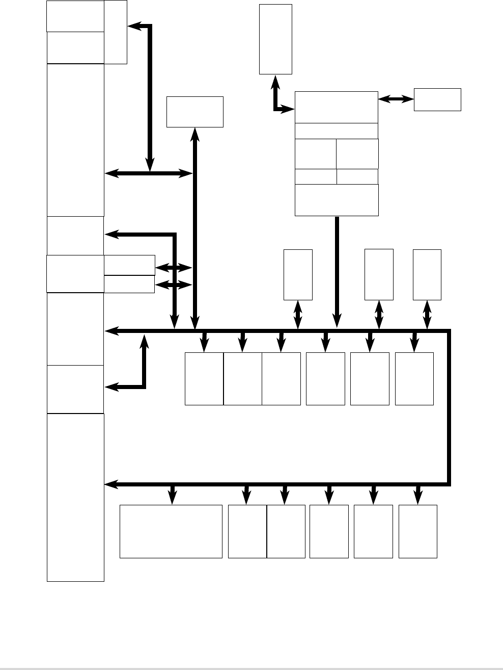
MOTOROLA Chapter 1. Overview 1-7
MCF5282 Key Features
Figure 1-1. MCF5282 Block Diagram
Interface
Chip
UART1
Serial
I/O
JTAG
Port
Selects
ColdFire V2 Core
EMAC
External
Test
Controller
I2C
Module
UART2
Serial
I/O
DMA
Timer
Modules
DRAM
Controller
2-Kbyte
D-Cache/I-Cache
Debug Module
DIV
Clock Module
Chip
Configuration
Reset
Controller
Power
(PLL)
Edgeport
Interrupt
Controller 0
Interrupt
Controller 1
FEC
UART0
Serial
I/O
DMA
Controller
Watchdog
Timer
General
Purpose
Timer A
General
Purpose
Timer B
QSPI FlexCANQADC
PIT
Timers
(PIT0–
(DTIM0–
DTIM3)
Management
Module
Ports
Module
PIT3)
Internal Bus
Arbiter
System
Control
Module (SCM)
Flash
Module
64K
SRAM

1-8 MCF5282 User’s Manual MOTOROLA
MCF5282 Key Features
1.1.1 Version 2 ColdFire Core
The processor core is comprised of two separate pipelines that are decoupled by an
instruction buffer. The two-stage instruction fetch pipeline (IFP) is responsible for
instruction-address generation and instruction fetch. The instruction buffer is a
first-in-first-out (FIFO) buffer that holds prefetched instructions awaiting execution in the
operand execution pipeline (OEP). The OEP includes two pipeline stages. The first stage
decodes instructions and selects operands (DSOC); the second stage (AGEX) performs
instruction execution and calculates operand effective addresses, if needed.
The V2 core implements the ColdFire instruction set architecture revision A with added
support for a separate user stack pointer register and four new instructions to assist in bit
processing. Additionally, the MCF5282 core includes the enhanced multiply-accumulate
unit (EMAC) for improved signal processing capabilities. The EMAC implements a
4-stage execution pipeline, optimized for 32 x 32 bit operations, with support for four 48-bit
accumulators. Supported operands include 16- and 32-bit signed and unsigned integers,
signed fractional operands, and a complete set of instructions to process these data types.
The EMAC provides superb support for execution of DSP operations within the context of
a single processor at a minimal hardware cost.
1.1.1.1 Cache
The 2-Kbyte cache can be configured into one of three possible organizations: a 2-Kbyte
instruction cache, a 2-Kbyte data cache or a split 1-Kbyte instruction/1-Kbyte data cache.
The configuration is software-programmable by control bits within the privileged cache
configuration register (CACR). In all configurations, the cache is a direct-mapped
single-cycle memory, organized as 128 lines, each containing 16 bytes of data. The
memories consist of a 128-entry tag array (containing addresses and control bits) and a
2-Kbyte data array, organized as 512 x 32 bits. The tag and data arrays are accessed in
parallel using the following address bits:
If the desired address is mapped into the cache memory, the output of the data array is
driven onto the ColdFire core's local data bus, completing the access in a single cycle. If
the data is not mapped into the tag memory, a cache miss occurs and the processor core
initiates a 16-byte line-sized fetch. The cache module includes a 16-byte line fill buffer used
Table 1-1. Cache Configuration
Configuration Tag Address Data Array Address
2 Kbyte I-Cache [10:4] [10:2]
2 Kbyte D-Cache [10:4] [10:2]
Split I-/D-Cache 0
Instruction Fetches
Operand Accesses
0, [9:4]
1, [9:4]
0, [9:2]
1, [9:2]

MOTOROLA Chapter 1. Overview 1-9
MCF5282 Key Features
as temporary storage during miss processing. For all data cache configurations, the memory
operates in write-through mode and all operand writes generate an external bus cycle.
1.1.1.2 SRAM
The SRAM module provides a general-purpose 64-Kbyte memory block that the ColdFire
core can access in a single cycle. The location of the memory block can be set to any
64-Kbyte boundary within the 4-Gbyte address space. The memory is ideal for storing
critical code or data structures, for use as the system stack, or for storing FEC data buffers.
Because the SRAM module is physically connected to the processor's high-speed local bus,
it can quickly service core-initiated accesses or memory-referencing commands from the
debug module.
The SRAM module is also accessible by non-core bus masters, for example the DMA
and/or the FEC. The dual-ported nature of the SRAM makes it ideal for implementing
applications with double-buffer schemes, where the processor and a DMA device operate
in alternate regions of the SRAM to maximize system performance. As an example, system
performance can be increased significantly if Ethernet packets are moved from the FEC
into the SRAM (rather than external memory) prior to any processing.
1.1.1.3 Flash
This product incorporates SuperFlash® technology licensed from SST. The ColdFire Flash
Module (CFM) is a non-volatile memory (NVM) module for integration with the processor
core. The CFM is constructed with eight banks of 32K x 16-bit Flash arrays to generate
512 Kbytes of 32-bit Flash memory
NOTE
The CFM on the MCF5281 is constructed with four banks of
32K x 16-bit Flash arrays to generate 256 Kbytes of 32-bit
Flash memory.
These arrays serve as electrically erasable and programmable, non-volatile program and
data memory. The Flash memory is ideal for program and data storage for single-chip
applications allowing for field reprogramming without requiring an external programming
voltage source. The CFM interfaces to the V2 ColdFire core through an optimized
read-only memory controller which supports interleaved accesses from the 2-cycle Flash
arrays. A “backdoor” mapping of the Flash memory is used for all program, erase, and
verify operations. It also provides a read datapath for non-core masters (for example,
DMA).
1.1.1.4 Debug Module
The ColdFire processor core debug interface is provided to support system debugging in
conjunction with low-cost debug and emulator development tools. Through a standard

1-10 MCF5282 User’s Manual MOTOROLA
MCF5282 Key Features
debug interface, users can access real-time trace and debug information. This allows the
processor and system to be debugged at full speed without the need for costly in-circuit
emulators. The debug interface is a superset of the BDM interface provided on Motorola’s
683xx family of parts.
The on-chip breakpoint resources include a total of 6 programmable registers—a set of
address registers (with two 32-bit registers), a set of data registers (with a 32-bit data
register plus a 32-bit data mask register), and one 32-bit PC register plus a 32-bit PC mask
register. These registers can be accessed through the dedicated debug serial communication
channel or from the processor’s supervisor mode programming model. The breakpoint
registers can be configured to generate triggers by combining the address, data, and PC
conditions in a variety of single or dual-level definitions. The trigger event can be
programmed to generate a processor halt or initiate a debug interrupt exception.
To support program trace, the Version 2 debug module provides processor status (PST[3:0])
and debug data (DDATA[3:0]) ports. These buses and the CLKOUT output provide
execution status, captured operand data, and branch target addresses defining the dynamic
execution path of the processor at the CPU’s clock rate.
1.1.2 System Control Module
This section details the functionality of the System Control Module (SCM) which provides
the programming model for the System Access Control Unit (SACU), the system bus
arbiter, a 32-bit Core Watchdog Timer (CWT), and the system control registers and logic.
Specifically, the system control includes the internal peripheral system base address
register (IPSBAR), the processor’s dual-port RAM base address register (RAMBAR), and
system control registers that include low-power and core watchdog timer control.
1.1.3 External Interface Module (EIM)
The external interface module handles the transfer of information between the internal core
and memory, peripherals, or other processing elements in the external address space.
Programmable chip-select outputs provide signals to enable external memory and
peripheral circuits, providing all handshaking and timing signals for automatic wait-state
insertion and data bus sizing.
Base memory address and block size are programmable, with some restrictions. For
example, the starting address must be on a boundary that is a multiple of the block size.
Each chip select can be configured to provide read and write enable signals suitable for use
with most popular static RAMs and peripherals. Data bus width (8-bit, 16-bit, or 32-bit) is
programmable on all chip selects, and further decoding is available for protection from user
mode access or read-only access.

MOTOROLA Chapter 1. Overview 1-11
MCF5282 Key Features
1.1.4 Chip Select
Programmable chip select outputs provide a glueless connection to external memory and
peripheral circuits, providing all handshaking and timing signals for automatic wait-state
insertion and data bus sizing.
1.1.5 Power Management
The MCF5282 incorporates several low-power modes of operation which are entered under
program control and exited by several external trigger events. An integrated Power-On
Reset (POR) circuit monitors the input supply and forces an MCU reset as the supply
voltage rises. The Low Voltage Detect (LVD) section monitors the supply voltage and is
configurable to force a reset or interrupt condition if it falls below the LVD trip point. The
RAM standby switch provides power to RAM when the supply voltage is higher than the
standby voltage. If the supply voltage to chip falls below the standby battery voltage, the
RAM is switched over to the standby supply.
1.1.6 General Input/Output Ports
All of the pins associated with the external bus interface may be used for several different
functions. Their primary function is to provide an external memory interface to access
off-chip resources. When not used for this function, all of the pins may be used as
general-purpose digital I/O pins. In some cases, the pin function is set by the operating
mode, and the alternate pin functions are not supported.
The digital I/O pins on the MCF5282 are grouped into 8-bit ports. Some ports do not use
all eight bits. Each port has registers that configure, monitor, and control the port pins.
1.1.7 Interrupt Controllers (INTC0/INTC1)
There are two interrupt controllers on the MCF5282, each of which can support up to 63
interrupt sources for a total of 126. Each interrupt controller is organized as 7 levels with 9
interrupt sources per level. Each interrupt source has a unique interrupt vector, and 56 of
the 63 sources of a given controller provide a programmable level [1-7] and priority within
the level.
1.1.8 SDRAM Controller
The SDRAM controller provides all required signals for glueless interfacing to a variety of
JEDEC-compliant SDRAM devices. SRAS/SCAS address multiplexing is software
configurable for different page sizes. To maintain refresh capability without conflicting
with concurrent accesses on the address and data buses, SRAS, SCAS, DRAMW,
SDRAM_CS[1:0], and SCKE are dedicated SDRAM signals.

1-12 MCF5282 User’s Manual MOTOROLA
MCF5282 Key Features
1.1.9 Test Access Port
The MCF5282 supports circuit board test strategies based on the Test Technology
Committee of IEEE and the Joint Test Action Group (JTAG). The test logic includes a test
access port (TAP) consisting of a 16-state controller, an instruction register, and three test
registers (a 1-bit bypass register, a 256-bit boundary-scan register, and a 32-bit ID register).
The boundary scan register links the device’s pins into one shift register. Test logic,
implemented using static logic design, is independent of the device system logic.
The MCF5282 implementation supports the following:
• Perform boundary-scan operations to test circuit board electrical continuity
• Sample MCF5282 system pins during operation and transparently shift out the result
in the boundary scan register
• Bypass the MCF5282 for a given circuit board test by effectively reducing the
boundary-scan register to a single bit
• Disable the output drive to pins during circuit-board testing
• Drive output pins to stable levels
1.1.10 UART Modules
The MCF5282 contains three full-duplex UARTs that function independently. The three
UARTs can be clocked by the system clock, eliminating the need for an external crystal.
Each UART has the following features:
• Each can be clocked by the system clock, eliminating a need for an external UART
clock
• Full-duplex asynchronous/synchronous receiver/transmitter channel
• Quadruple-buffered receiver
• Double-buffered transmitter
• Independently programmable receiver and transmitter clock sources
• Programmable data format:
— 5–8 data bits plus parity
— Odd, even, no parity, or force parity
— One, one-and-a-half, or two stop bits
• Each channel programmable to normal (full-duplex), automatic echo, local
loop-back, or remote loop-back mode
• Automatic wake-up mode for multidrop applications
• Four maskable interrupt conditions
• All three UARTs have DMA request capability

MOTOROLA Chapter 1. Overview 1-13
MCF5282 Key Features
• Parity, framing, and overrun error detection
• False-start bit detection
• Line-break detection and generation
• Detection of breaks originating in the middle of a character
• Start/end break interrupt/status
1.1.11 DMA Timers (DTIM0-DTIM3)
There are four independent, DMA-transfer-generating 32-bit timers (DTIM0, DTIM1,
DTIM2, DTIM3) on the MCF5282. Each timer module incorporates a 32-bit timer with a
separate register set for configuration and control. The timers can be configured to operate
from the system clock or from an external clock source using one of the DTINx signals. If
the system clock is selected, it can be divided by 16 or 1. The selected clock is further
divided by a user-programmable 8-bit prescaler which clocks the actual timer counter
register (TCRn). Each of these timers can be configured for input capture or reference
compare mode. By configuring the internal registers, each timer may be configured to
assert an external signal, generate an interrupt on a particular event, or cause a DMA
transfer.
1.1.12 General-Purpose Timers (GPTA/GPTB)
The two general-purpose timers (GPTA and GPTB) are 4-channel timer modules. Each
timer consists of a 16-bit programmable counter driven by a 7-stage programmable
prescaler. Each of the four channels for each timer can be configured for input capture or
output compare. Additionally, one of the channels, channel 3, can be configured as a pulse
accumulator.
A timer overflow function allows software to extend the timing capability of the system
beyond the 16-bit range of the counter. The input capture and output compare functions
allow simultaneous input waveform measurements and output waveform generation. The
input capture function can capture the time of a selected transition edge. The output
compare function can generate output waveforms and timer software delays. The 16-bit
pulse accumulator can operate as a simple event counter or a gated time accumulator.
1.1.13 Periodic Interrupt Timers (PIT0-PIT3)
The four periodic interrupt timers (PIT0, PIT1, PIT2, PIT3) are 16-bit timers that provide
precise interrupts at regular intervals with minimal processor intervention. Each timer can
either count down from the value written in its PIT modulus register, or it can be a
free-running down-counter.

1-14 MCF5282 User’s Manual MOTOROLA
MCF5282 Key Features
1.1.14 Software Watchdog Timer
The watchdog timer is a 16-bit timer that facilitates recovery from runaway code. The
watchdog counter is a free-running down-counter that generates a reset on underflow. To
prevent a reset, software must periodically restart the countdown.
1.1.15 Phase Locked Loop (PLL)
The clock module contains a crystal oscillator (OSC), phase-locked loop (PLL), reduced
frequency divider (RFD), status/control registers, and control logic. To improve noise
immunity, the PLL and OSC have their own power supply inputs, VDDPLL and VSSPLL.
All other circuits are powered by the normal supply pins, VDD and VSS.
1.1.16 DMA Controller
The Direct Memory Access (DMA) controller module provides an efficient way to move
blocks of data with minimal processor interaction. The DMA module provides four
channels (DMA0–DMA3) that allow byte, word, longword or 16-byte burst line transfers.
These transfers are triggered by software, explicitly setting a DCRn[START] bit or the
occurrence of a hardware event from one of the on-chip peripheral devices, such as a
capture event or an output reference event in a DMA timer (DTIMn) for each channel. The
DMA controller supports dual-address mode to on-chip devices.
1.1.17 Reset
The reset controller is provided to determine the cause of reset, assert the appropriate reset
signals to the system, and keep track of what caused the last reset. The power management
registers for the internal low-voltage detect (LVD) circuit are implemented in the reset
module. There are seven sources of reset:
• External
• Power-on reset (POR)
• Watchdog timer
• Phase-locked loop (PLL) loss of lock
• PLL loss of clock
• Software
• Low-voltage detection (LVD) reset
External reset on the RSTO pin is software-assertable independent of chip reset state. There
are also software-readable status flags indicating the cause of the last reset, and LVD
control and status bits for setup and use of LVD reset or interrupt.

MOTOROLA Chapter 1. Overview 1-15
MCF5282-Specific Features
1.2 MCF5282-Specific Features
1.2.1 Fast Ethernet Controller (FEC)
The MCF5282’s integrated Fast Ethernet Controller (FEC) performs the full set of IEEE
802.3/Ethernet CSMA/CD media access control and channel interface functions. The FEC
supports connection and functionality for the 10/100 Mbps 802.3 media independent
interface (MII). It requires an external transceiver (PHY) to complete the interface to the
media.
1.2.2 FlexCAN
The FlexCAN module is a communication controller implementing the CAN protocol. The
CAN protocol can be used as an industrial control serial data bus, meeting the specific
requirements of real-time processing, reliable operation in a harsh EMI environment,
cost-effectiveness, and required bandwidth. FlexCAN contains 16 message buffers.
1.2.3 I2C Bus
The I2C bus is a two-wire, bidirectional serial bus that provides a simple, efficient method
of data exchange, minimizing the interconnection between devices. This bus is suitable for
applications requiring occasional communications over a short distance between many
devices.
1.2.4 Queued Serial Peripheral Interface (QSPI)
The queued serial peripheral interface module provides a synchronous serial peripheral
interface with queued transfer capability. It allows up to 16 transfers to be queued at once,
eliminating CPU intervention between transfers.
1.2.5 Queued Analog-to-Digital Converter (QADC)
The QADC is a 10-bit, unipolar, successive approximation converter. A maximum of 8
analog input channels can be supported using internal multiplexing. A maximum of 18
input channels can be supported in the internal/external multiplexed mode.
The QADC consists of an analog front-end and a digital control subsystem. The analog
section includes input pins, an analog multiplexer, and sample and hold analog circuits. The
analog conversion is performed by the digital-to-analog converter (DAC) resistor-capacitor
array and a high-gain comparator.
The digital control section contains queue control logic to sequence the conversion process
and interrupt generation logic. Also included are the periodic/interval timer, control and

1-16 MCF5282 User’s Manual MOTOROLA
MCF5282-Specific Features
status registers, the 64-entry conversion command word (CCW) table, and the 64-entry
result table.
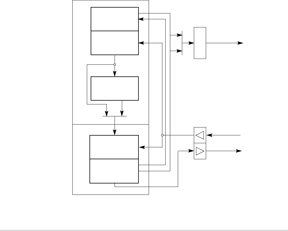
MOTOROLA Chapter 2. ColdFire Core 2-1
Chapter 2
ColdFire Core
This section describes the organization of the Version 2 (V2) ColdFire® processor core and
an overview of the program-visible registers. For detailed information on instructions, see
the ColdFire Family Programmer’s Reference Manual.
2.1 Processor Pipelines
Figure 2-1 is a block diagram showing the processor pipelines of a V2 ColdFire core.
Figure 2-1. ColdFire Processor Core Pipelines
Instruction
Instruction
FIFO
Decode & Select,
Address
read_data[31:0]
IAG
IC
IB
DSOC
AGEX
Address [31:0]
Instruction Buffer
Address
Generation
Fetch Cycle
Generation,
Execute
Operand Fetch
Operand
Execution
Pipeline
Instruction
Fetch
Pipeline
write_data[31:0]

2-2 MCF5282 User’s Manual MOTOROLA
Processor Register Description
The processor core is comprised of two separate pipelines that are decoupled by an
instruction buffer.
The Instruction Fetch Pipeline (IFP) is a two-stage pipeline for prefetching instructions.
The prefetched instruction stream is then gated into the two-stage Operand Execution
Pipeline (OEP), which decodes the instruction, fetches the required operands and then
executes the required function. Since the IFP and OEP pipelines are decoupled by an
instruction buffer which serves as a FIFO queue, the IFP is able to prefetch instructions in
advance of their actual use by the OEP thereby minimizing time stalled waiting for
instructions.
The Instruction Fetch Pipeline consists of two stages with an instruction buffer stage:
• Instruction Address Generation (IAG Cycle)
• Instruction Fetch Cycle (IC Cycle)
• Instruction Buffer (IB Cycle)
When the instruction buffer is empty, opcodes are loaded directly from the IC cycle into the
Operand Execution Pipeline. If the buffer is not empty, the IFP stores the contents of the
fetch cycle in the FIFO queue until it is required by the OEP. In the Version 2
implementation, the instruction buffer contains three 32-bit longwords of storage.
The Operand Execution Pipeline is implemented in a two-stage pipeline featuring a
traditional RISC datapath with a dual-read-ported register file (RGF) feeding an
arithmetic/logic unit. In this design, the pipeline stages have multiple functions:
• Decode & Select/Operand Cycle (DSOC Cycle)
• Address Generation/Execute Cycle (AGEX Cycle)
2.2 Processor Register Description
The following paragraphs describe the processor registers in the user and supervisor
programming models. The appropriate programming model is selected based on the
privilege level (user mode or supervisor mode) of the processor as defined by the S bit of
the status register (SR).
2.2.1 User Programming Model
Figure 2-2 illustrates the user programming model. The model is the same as the M68000
family microprocessors, consisting of the following registers:
• 16 general-purpose 32-bit registers (D0–D7, A0–A7)
• 32-bit program counter (PC)
• 8-bit condition code register (CCR)

MOTOROLA Chapter 2. ColdFire Core 2-3
Processor Register Description
2.2.1.1 Data Registers (D0–D7)
Registers D0–D7 are used as data registers for bit (1-bit), byte (8-bit), word (16-bit) and
longword (32-bit) operations; they can also be used as index registers.
2.2.1.2 Address Registers (A0–A6)
These registers can be used as software stack pointers, index registers, or base address
registers; they can also be used for word and longword operations.
2.2.1.3 Stack Pointer (A7)
Certain ColdFire implementations, including the MCF5282, support two unique stack
pointer (A7) registers—the supervisor stack pointer (SSP) and the user stack pointer (USP).
This support provides the required isolation between operating modes of the processor. The
SSP is described in Section 2.2.3.2, “Supervisor/User Stack Pointers (A7 and
OTHER_A7).”
A subroutine call saves the PC on the stack and the return restores it from the stack. Both
the PC and the SR are saved on the supervisor stack during the processing of exceptions
and interrupts. The return from exception (RTE) instruction restores the SR and PC values
from the supervisor stack.
2.2.1.4 Program Counter (PC)
The PC contains the address of the currently executing instruction. During instruction
execution and exception processing, the processor automatically increments the contents of
the PC or places a new value in the PC, as appropriate. For some addressing modes, the PC
is used as a base address for PC-relative operand addressing.
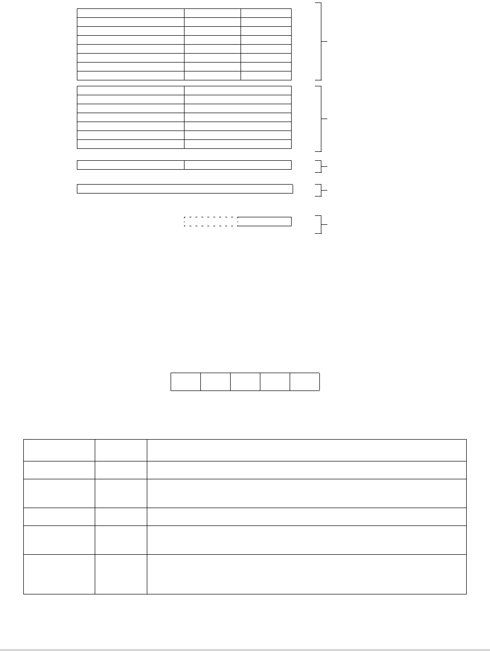
2-4 MCF5282 User’s Manual MOTOROLA
Processor Register Description
Figure 2-2. User Programming Model
2.2.1.5 Condition Code Register (CCR)
The CCR is the LSB of the processor status register (SR). Bits 4–0 act as indicator flags for
results generated by processor operations. Bit 4, the extend bit (X bit), is also used as an
input operand during multiprecision arithmetic computations.
43210
XNZVC
Figure 2-3. Condition Code Register (CCR)
Table 2-1. CCR Field Descriptions
Bits Name Description
4 X Extend condition code bit.
3 N Negative condition code bit. Set if the most significant bit of the result is set;
otherwise cleared.
2 Z Zero condition code bit. Set if the result equals zero; otherwise cleared.
1 V Overflow condition code bit. Set if an arithmetic overflow occurs implying that the
result cannot be represented in the operand size; otherwise cleared.
0 C Carry condition code bit. Set if a carry out of the operand msb occurs for an
addition, or if a borrow occurs in a subtraction; otherwise cleared
Set to the value of the C bit for arithmetic operations; otherwise not affected.
D0
D1
D2
D3
D4
D5
D6
D7
A0
A1
A2
A3
A4
A5
A6
A7
CCR
PC
15 7 0
15 031
DATA
REGISTERS
ADDRESS
REGISTERS
USERSTACK
POINTER
PROGRAM
COUNTER
CONDITION
CODE
REGISTER
7

MOTOROLA Chapter 2. ColdFire Core 2-5
Processor Register Description
2.2.2 EMAC Programming Model
The registers in the EMAC portion of the user programming model, are described in
Section Chapter 5, “Enhanced Multiply-Accumulate Unit (EMAC),” and include the
following registers:
• Four 48-bit accumulator registers partitioned as follows:
— Four 32-bit accumulators (ACC0–ACC3)
— Eight 8-bit accumulator extension bytes (two per accumulator). These are
grouped into two 32-bit values for load and store operations (ACCEXT01 and
ACCEXT23).
Accumulators and extension bytes can be loaded, copied, and stored, and results
from EMAC arithmetic operations generally affect the entire 48-bit destination.
• Eight 8-bit accumulator extensions (two per accumulator), packaged as two 32-bit
values for load and store operations (ACCext01 and ACCext23)
• One 16-bit mask register (MASK)
• One 32-bit status register (MACSR) including four indicator bits signaling product
or accumulation overflow (one for each accumulator: PAV0–PAV3)
These registers are shown in Figure 2-4.
Figure 2-4. EMAC Register Set
2.2.3 Supervisor Programming Model
Only system control software is intended to use the supervisor programming model to
implement restricted operating system functions, I/O control, and memory management.
All accesses that affect the control features of ColdFire processors are in the supervisor
programming model, which consists of registers available in user mode as well as the
following control registers:
• 16-bit status register (SR)
• 32-bit supervisor stack pointer (SSP)
• 32-bit vector base register (VBR)
• 32-bit cache control register (CACR)
31 0
MACSR MAC status register
ACC0 MAC accumulator 0
ACC1 MAC accumulator 1
ACC2 MAC accumulator 2
ACC3 MAC accumulator 3
ACCext01 Extensions for ACC0 and ACC1
ACCext23 Extensions for ACC2 and ACC3
MASK MAC mask register

2-6 MCF5282 User’s Manual MOTOROLA
Processor Register Description
• Two 32-bit access control registers (ACR0, ACR1)
• Two 32-bit memory base address registers (RAMBAR, FLASHBAR)
Figure 2-5. Supervisor Programming Model
The following paragraphs describe the supervisor programming model registers.
2.2.3.1 Status Register (SR)
The SR stores the processor status and includes the CCR, the interrupt priority mask, and
other control bits. In supervisor mode, software can access the entire SR. In user mode, only
the lower 8 bits are accessible (CCR). The control bits indicate the following states for the
processor: trace mode (T bit), supervisor or user mode (S bit), and master or interrupt state
(M bit). All defined bits in the SR have read/write access when in supervisor mode.
System Byte Condition Code Register (CCR)
151413121110 876543210
T0SM0 I 000XNZVC
Figure 2-6. Status Register
Table 2-2. SR Field Descriptions
Bits Name Description
15 T Trace enable. When set, the processor performs a trace exception after
every instruction.
14 — Reserved, should be cleared.
13 S Supervisor/user state. Denotes whether the processor is in supervisor
mode (S = 1) or user mode (S = 0).
SR
15 7 0
31
STATUS
(CCR)
OTHER_A7 SUPERVISOR A7
STACK POINTER
VBR VECTOR BASE
REGISTER
CACR CACHE
CONTROL
ACR0 ACCESS
CONTROL
ACR1 ACCESS
CONTROL
FLASHBAR FLASH BASE
ADDRESS REGISTER
RAMBAR RAM BASE
ADDRESS REGISTER

MOTOROLA Chapter 2. ColdFire Core 2-7
Processor Register Description
2.2.3.2 Supervisor/User Stack Pointers (A7 and OTHER_A7)
The MCF5282 architecture supports two independent stack pointer (A7) registers—the
supervisor stack pointer (SSP) and the user stack pointer (USP). The hardware
implementation of these two programmable-visible 32-bit registers does not identify one as
the SSP and the other as the USP. Instead, the hardware uses one 32-bit register as the active
A7 and the other as OTHER_A7. Thus, the register contents are a function of the processor
operation mode, as shown in the following:
if SR[S] = 1
then A7 = Supervisor Stack Pointer
OTHER_A7 = User Stack Pointer
else A7 = User Stack Pointer
OTHER_A7 = Supervisor Stack Pointer
The BDM programming model supports direct reads and writes to A7 and OTHER_A7. It
is the responsibility of the external development system to determine, based on the setting
of SR[S], the mapping of A7 and OTHER_A7 to the two program-visible definitions (SSP
and USP). This functionality is enabled by setting the enable user stack pointer bit,
CACR[EUSP]. If this bit is cleared, only the stack pointer (A7), defined for previous
ColdFire versions, is available. EUSP is zero at reset.
If EUSP is set, the appropriate stack pointer register (SSP or USP) is accessed as a function
of the processor’s operating mode. To support dual stack pointers, the following two
privileged M68000 instructions are added to the ColdFire instruction set architecture to
load/store the USP :
move.l Ay, USP; move to USP
move.l USP, Ax; move from USP
These instructions are described in the ColdFire Family Programmer’s Reference Manual.
12 M Master/interrupt state. This bit is cleared by an interrupt exception, and
can be set by software during execution of the RTE or move to SR
instructions.
11 — Reserved, should be cleared.
10–8 I Interrupt level mask. Defines the current interrupt level. Interrupt
requests are inhibited for all priority levels less than or equal to the
current level, except the edge-sensitive level 7 request, which cannot
be masked.
7–5 — Reserved, should be cleared.
4–0 CCR Refer to Table 2-1.
Table 2-2. SR Field Descriptions (continued)
Bits Name Description

2-8 MCF5282 User’s Manual MOTOROLA
Programming Model
2.2.3.3 Vector Base Register (VBR)
The VBR contains the base address of the exception vector table in memory. To access the
vector table, the displacement of an exception vector is added to the value in VBR. The
lower 20 bits of the VBR are not implemented by ColdFire processors; they are assumed to
be zero, forcing the table to be aligned on a 1 MByte boundary.
2.2.3.4 Cache Control Register (CACR)
The CACR controls operation of the instruction/data cache memories. It includes bits for
enabling, freezing, and invalidating cache contents. It also includes bits for defining the
default cache mode and write-protect fields. The CACR is described in Section 4.4.2.1,
“Cache Control Register (CACR).”
2.2.3.5 Access Control Registers (ACR0, ACR1)
The access control registers, ACR0 and ACR1, define attributes for two user-defined
memory regions. These attributes include the definition of cache mode, write protect, and
buffer write enables. The ACRs are described in Section 4.4.2.2, “Access Control Registers
(ACR0, ACR1).”
2.2.3.6 Memory Base Address Registers (RAMBAR, FLASHBAR)
Memory base address registers are used to specify the base address of the internal SRAM
and Flash modules and indicate the types of references mapped to each. Each base address
register includes a base address, write-protect bit, address space mask bits, and an enable
bit. For the MCF5282, FLASHBAR determines the base address of the on-chip Flash, and
RAMBAR determines the base address of the on-chip RAM. For more information, refer
to Section 5.3.1, “SRAM Base Address Register (RAMBAR)” and Section 6.3.2, “Flash
Base Address Register (FLASHBAR).”
2.3 Programming Model
Table 2-3 lists register names, the CPU space location, and whether the register is written
from the processor using the MOVEC instruction.
Table 2-3. ColdFire CPU Registers
Name CPU Space (Rc) Written with
MOVEC Register Name
Memory Management Control Registers
CACR 0x002 Yes Cache control register
ACR0, ACR1 0x004-0x005 Yes Access control registers 0 and 1
Processor General-Purpose Registers

MOTOROLA Chapter 2. ColdFire Core 2-9
Additions to the Instruction Set Architecture
2.4 Additions to the Instruction Set Architecture
The original ColdFire instruction set architecture (ISA) was derived from the
M68000-family opcodes based on extensive analysis of embedded application code. After
the initial ColdFire compilers were created, developers identified ISA additions that would
enhance both code density and overall performance. Additionally, as users implemented
ColdFire-based designs into a wide range of embedded systems, they identified frequently
used instruction sequences that could be improved by the creation of new instructions. This
observation was especially prevalent in development environments that made use of
substantial amounts of assembly language code.
Table 2-4 summarizes the new instructions added to Revision A+ ISA. For more details see
Section 2.14, “ColdFire Instruction Set Architecture Enhancements.”
D0-D7 0x(0,1)80-0x(0,1)87 No Data registers 0-7 (0 = load, 1 = store)
A0-A7 0x(0,1)88-0x(0,1)8F No Address registers 0-7 (0 = load, 1 = store)
A7 is user stack pointer
Processor Miscellaneous Registers
OTHER_A7 0x800 No Other stack pointer
VBR 0x801 Yes Vector base register
MACSR 0x804 No MAC status register
MASK 0x805 No MAC address mask register
ACC0-ACC3 0x806, 0x809,
0x80A, 0x80B
No MAC accumulators 0-3
ACCext01 0x807 No MAC accumulator 0, 1 extension bytes
ACCext23 0x808 No MAC accumulator 2, 3 extension bytes
SR 0x80E No Status register
PC 0x80F Yes Program counter
Local Memory Registers
FLASHBAR 0xC04 Yes Flash base address register
RAMBAR 0xC05 Yes SRAM base address register
Table 2-3. ColdFire CPU Registers (continued)
Name CPU Space (Rc) Written with
MOVEC Register Name

2-10 MCF5282 User’s Manual MOTOROLA
Exception Processing Overview
2.5 Exception Processing Overview
Exception processing for ColdFire processors is streamlined for performance. The
ColdFire processors differ from the M68000 family in that they include:
• A simplified exception vector table
• Reduced relocation capabilities using the vector base register
• A single exception stack frame format
• Use of a single self-aligning system stack
All ColdFire processors use an instruction restart exception model, but certain
microarchitectures (V2 and V3) require more software support to recover from certain
access errors. See Section 2.7.1, “Access Error Exception” for details.
Exception processing includes all actions from the detection of the fault condition to the
initiation of fetch for the first handler instruction. Exception processing is comprised of
four major steps
First, the processor makes an internal copy of the SR and then enters supervisor mode by
asserting the S bit and disabling trace mode by negating the T bit. The occurrence of an
interrupt exception also forces the M bit to be cleared and the interrupt priority mask to be
set to the level of the current interrupt request.
Second, the processor determines the exception vector number. For all faults except
interrupts, the processor performs this calculation based on the exception type. For
interrupts, the processor performs an interrupt-acknowledge (IACK) bus cycle to obtain the
vector number from the interrupt controller. The IACK cycle is mapped to a special
acknowledge address space with the interrupt level encoded in the address.
Table 2-4. ISA Revision A+ New Instructions
Instruction Description
BITREV The contents of the destination data register are bit-reversed; that
is, new Dx[31] = old Dx[0], new Dx[30] = old Dx[1], ..., new Dx[0]
= old Dx[31].
BYTEREV The contents of the destination data register are byte-reversed;
that is, new Dx[31:24] = old Dx[7:0], ..., new Dx[7:0] = old
Dx[31:24].
FF1 The data register, Dx, is scanned, beginning from the
most-significant bit (Dx[31]) and ending with the least-significant
bit (Dx[0]), searching for the first set bit. The data register is then
loaded with the offset count from bit 31 where the first set bit
appears.
STLDSR Pushes the contents of the Status Register onto the stack and
then reloads the Status Register with the immediate data value.

MOTOROLA Chapter 2. ColdFire Core 2-11
Exception Processing Overview
Third, the processor saves the current context by creating an exception stack frame on the
supervisor system stack. As a result, the exception stack frame is created at a 0-modulo-4
address on the top of the current system stack. Additionally, the processor uses a simplified
fixed-length stack frame for all exceptions. The exception type determines whether the
program counter placed in the exception stack frame defines the location of the faulting
instruction (fault) or the address of the next instruction to be executed (next).
Fourth, the processor calculates the address of the first instruction of the exception handler.
By definition, the exception vector table is aligned on a 1 Mbyte boundary. This instruction
address is generated by fetching an exception vector from the table located at the address
defined in the vector base register. The index into the exception table is calculated as (4 x
vector number). Once the exception vector has been fetched, the contents of the vector
determine the address of the first instruction of the desired handler. After the instruction
fetch for the first opcode of the handler has been initiated, exception processing terminates
and normal instruction processing continues in the handler.
All ColdFire processors support a 1024-byte vector table aligned on any 1 Mbyte address
boundary (see Table 2-5). The table contains 256 exception vectors; the first 64 are defined
by Motorola and the remaining 192 are user-defined interrupt vectors.
Table 2-5. Exception Vector Assignments
Vector
Number(S)
Vector
Offset (Hex)
Stacked
Program
Counter
Assignment
0 0x000 — Initial stack pointer
1 0x004 — Initial program counter
2 0x008 Fault Access error
3 0x00C Fault Address error
4 0x010 Fault Illegal instruction
5 0x014 Fault Divide by zero
6–7 0x018–0x01C — Reserved
8 0x020 Fault Privilege violation
9 0x024 Next Trace
10 0x028 Fault Unimplemented line-a opcode
11 0x02C Fault Unimplemented line-f opcode
12 0x030 Next Debug interrupt
13 0x034 — Reserved
14 0x038 Fault Format error
15–23 0x03C–0x05C — Reserved
24 0x060 Next Spurious interrupt
25–31 0x064-0x07C — Reserved
32–47 0x080–0x0BC Next Trap # 0-15 instructions
48–63 0x0C0–0x0FC — Reserved
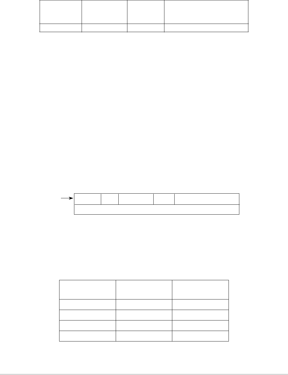
2-12 MCF5282 User’s Manual MOTOROLA
Exception Stack Frame Definition
All ColdFire processors inhibit interrupt sampling during the first instruction of all
exception handlers. This allows any handler to effectively disable interrupts, if necessary,
by raising the interrupt mask level contained in the status register. In addition, the V2 core
includes a new instruction (STLDSR) that stores the current interrupt mask level and loads
a value into the SR. This instruction is specifically intended for use as the first instruction
of an interrupt service routine which services multiple interrupt requests with different
interrupt levels. For more details see Section 2.14, “ColdFire Instruction Set Architecture
Enhancements.”
2.6 Exception Stack Frame Definition
The exception stack frame is shown in Figure 2-7. The first longword of the exception stack
frame contains the 16-bit format/vector word (F/V) and the 16-bit status register, and the
second longword contains the 32-bit program counter address.
Figure 2-7. Exception Stack Frame Form
The 16-bit format/vector word contains 3 unique fields:
• A 4-bit format field at the top of the system stack is always written with a value of
4, 5, 6, or 7 by the processor indicating a two-longword frame format. See Table 2-6.
64–255 0x100–0x3FC Next User-defined interrupts
“Fault” refers to the PC of the instruction that caused the exception; “Next” refers to the PC
of the next instruction that follows the instruction that caused the fault.
Table 2-6. Format Field Encodings
Original SSP @ Time
of Exception, Bits 1:0
SSP @ 1st Instruction
of Handler Format Field
00 Original SSP - 8 4
01 Original SSP - 9 5
10 Original SSP - 10 6
11 Original SSP - 11 7
Table 2-5. Exception Vector Assignments (continued)
Vector
Number(S)
Vector
Offset (Hex)
Stacked
Program
Counter
Assignment
FORMAT FS[3:2] VECTOR[7:0] FS[1:0] STATUS REGISTER
PROGRAM COUNTER[31:0]
SSP
+ 0X4
31 17 15 0
27 25

MOTOROLA Chapter 2. ColdFire Core 2-13
Processor Exceptions
• There is a 4-bit fault status field, FS[3:0], at the top of the system stack. This field is
defined for access and address errors only and written as zeros for all other types of
exceptions. See Table 2-7.
• The 8-bit vector number, vector[7:0], defines the exception type and is calculated by
the processor for all internal faults and represents the value supplied by the interrupt
controller in the case of an interrupt. Refer to Table 2-5.
2.7 Processor Exceptions
2.7.1 Access Error Exception
The exact processor response to an access error depends on the type of memory reference
being performed. For an instruction fetch, the processor postpones the error reporting until
the faulted reference is needed by an instruction for execution. Therefore, faults that occur
during instruction prefetches that are then followed by a change of instruction flow do not
generate an exception. When the processor attempts to execute an instruction with a faulted
opword and/or extension words, the access error is signaled and the instruction aborted. For
this type of exception, the programming model has not been altered by the instruction
generating the access error.
If the access error occurs on an operand read, the processor immediately aborts the current
instruction’s execution and initiates exception processing. In this situation, any address
register updates attributable to the auto-addressing modes, (for example, (An)+,-(An)),
have already been performed, so the programming model contains the updated An value.
In addition, if an access error occurs during the execution of a MOVEM instruction loading
from memory, any registers already updated before the fault occurs contain the operands
from memory.
Table 2-7. Fault Status Encodings
FS[3:0] Definition
00xx Reserved
0100 Error on instruction fetch
0101 Reserved
011x Reserved
1000 Error on operand write
1001 Attempted write to write-protected space
101x Reserved
1100 Error on operand read
1101 Reserved
111x Reserved

2-14 MCF5282 User’s Manual MOTOROLA
Processor Exceptions
The V2 ColdFire processor uses an imprecise reporting mechanism for access errors on
operand writes. Because the actual write cycle may be decoupled from the processor’s
issuing of the operation, the signaling of an access error appears to be decoupled from the
instruction that generated the write. Accordingly, the PC contained in the exception stack
frame merely represents the location in the program when the access error was signaled. All
programming model updates associated with the write instruction are completed. The NOP
instruction can collect access errors for writes. This instruction delays its execution until all
previous operations, including all pending write operations, are complete. If any previous
write terminates with an access error, it is guaranteed to be reported on the NOP instruction.
2.7.2 Address Error Exception
Any attempted execution transferring control to an odd instruction address (that is, if bit 0
of the target address is set) results in an address error exception.
Any attempted use of a word-sized index register (Xn.w) or a scale factor of 8 on an indexed
effective addressing mode generates an address error as does an attempted execution of a
full-format indexed addressing mode.
2.7.3 Illegal Instruction Exception
Any attempted execution of an illegal 16-bit opcode (except for line-A and line-F opcodes)
generates an illegal instruction exception (vector 4). Additionally, any attempted execution
of any non-MAC line-A and most line-F opcode generates their unique exception types,
vector numbers 10 and 11, respectively. The V2 core does not provide illegal instruction
detection on the extension words on any instruction, including MOVEC.
2.7.4 Divide-By-Zero
Attempting to divide by zero causes an exception (vector 5, offset = 0x014).
2.7.5 Privilege Violation
The attempted execution of a supervisor mode instruction while in user mode generates a
privilege violation exception. See the ColdFire Programmer’s Reference Manual for lists
of supervisor- and user-mode instructions.
2.7.6 Trace Exception
To aid in program development, all ColdFire processors provide an
instruction-by-instruction tracing capability. While in trace mode, indicated by the
assertion of the T-bit in the status register (SR[15] = 1), the completion of an instruction
execution (for all but the STOP instruction) signals a trace exception. This functionality
allows a debugger to monitor program execution.

MOTOROLA Chapter 2. ColdFire Core 2-15
Processor Exceptions
The STOP instruction has the following effects:
1. The instruction before the STOP executes and then generates a trace exception. In
the exception stack frame, the PC points to the STOP opcode.
2. When the trace handler is exited, the STOP instruction is executed, loading the SR
with the immediate operand from the instruction.
3. The processor then generates a trace exception. The PC in the exception stack
frame points to the instruction after the STOP, and the SR reflects the value loaded
in the previous step.
If the processor is not in trace mode and executes a STOP instruction where the immediate
operand sets SR[T], hardware loads the SR and generates a trace exception. The PC in the
exception stack frame points to the instruction after the STOP, and the SR reflects the value
loaded in step 2.
Because ColdFire processors do not support any hardware stacking of multiple exceptions,
it is the responsibility of the operating system to check for trace mode after processing other
exception types. As an example, consider the execution of a TRAP instruction while in
trace mode. The processor will initiate the TRAP exception and then pass control to the
corresponding handler. If the system requires that a trace exception be processed, it is the
responsibility of the TRAP exception handler to check for this condition (SR[15] in the
exception stack frame asserted) and pass control to the trace handler before returning from
the original exception.
2.7.7 Unimplemented Line-A Opcode
A line-A opcode is defined when bits 15-12 of the opword are 0b1010. This exception is
generated by the attempted execution of an undefined line-A opcode.
2.7.8 Unimplemented Line-F Opcode
A line-F opcode is defined when bits 15-12 of the opword are 0b1111. This exception is
generated by attempted execution of an undefined line-F opcode.
2.7.9 Debug Interrupt
This special type of program interrupt is discussed in detail in Chapter 29, “Debug
Support.” This exception is generated in response to a hardware breakpoint register trigger.
The processor does not generate an IACK cycle but rather calculates the vector number
internally (vector number 12).

2-16 MCF5282 User’s Manual MOTOROLA
Processor Exceptions
2.7.10 RTE and Format Error Exception
When an RTE instruction is executed, the processor first examines the 4-bit format field to
validate the frame type. For a ColdFire core, any attempted RTE execution where the
format is not equal to {4,5,6,7} generates a format error. The exception stack frame for the
format error is created without disturbing the original RTE frame and the stacked PC
pointing to the RTE instruction.
The selection of the format value provides some limited debug support for porting code
from M68000 applications. On M68000 family processors, the SR was located at the top of
the stack. On those processors, bit 30 of the longword addressed by the system stack pointer
is typically zero. Thus, if an RTE is attempted using this “old” format, it generates a format
error on a ColdFire processor.
If the format field defines a valid type, the processor: (1) reloads the SR operand, (2) fetches
the second longword operand, (3) adjusts the stack pointer by adding the format value to
the auto-incremented address after the fetch of the first longword, and then (4) transfers
control to the instruction address defined by the second longword operand within the stack
frame.
2.7.11 TRAP Instruction Exception
The TRAP #n instruction always forces an exception as part of its execution and is useful
for implementing system calls.
2.7.12 Interrupt Exception
Interrupt exception processing includes interrupt recognition and the fetch of the
appropriate vector from the interrupt controller using an IACK cycle. See Chapter 10,
“Interrupt Controller Modules” for details on the interrupt controller.
2.7.13 Fault-on-Fault Halt
If a ColdFire processor encounters any type of fault during the exception processing of
another fault, the processor immediately halts execution with the catastrophic
“fault-on-fault” condition. A reset is required to force the processor to exit this halted state.
2.7.14 Reset Exception
Asserting the reset input signal to the processor causes a reset exception. The reset
exception has the highest priority of any exception; it provides for system initialization and
recovery from catastrophic failure. Reset also aborts any processing in progress when the
reset input is recognized. Processing cannot be recovered.

MOTOROLA Chapter 2. ColdFire Core 2-17
Processor Exceptions
The reset exception places the processor in the supervisor mode by setting the S-bit and
disables tracing by clearing the T bit in the SR. This exception also clears the M-bit and sets
the processor’s interrupt priority mask in the SR to the highest level (level 7). Next, the
VBR is initialized to zero (0x00000000). The control registers specifying the operation of
any memories (e.g., cache and/or RAM modules) connected directly to the processor are
disabled.
NOTE
Other implementation-specific supervisor registers are also
affected. Refer to each of the modules in this user’s manual for
details on these registers.
Once the processor is granted the bus, it then performs two longword read bus cycles. The
first longword at address 0 is loaded into the stack pointer and the second longword at
address 4 is loaded into the program counter. After the initial instruction is fetched from
memory, program execution begins at the address in the PC. If an access error or address
error occurs before the first instruction is executed, the processor enters the fault-on-fault
halted state.
ColdFire processors load hardware configuration information into the D0 and D1
general-purpose registers after system reset. The hardware configuration information is
loaded immediately after the reset-in signal is negated. This allows an emulator to read out
the contents of these registers via BDM to determine the hardware configuration.
Information loaded into D0 defines the processor hardware configuration as shown in
Figure 2-8.
31 24 23 20 19 16
Field PF VER REV
Reset 1100_1111_0010_0000
R/W R
15 14 13 12 11 10 8 7 4 3 0
Field MAC DIV EMAC FPU MMU — ISA DEBUG
Reset 0110_0000_1000_0000
R/W R
Figure 2-8. D0 Hardware Configuration Info

2-18 MCF5282 User’s Manual MOTOROLA
Processor Exceptions
Information loaded into D1 defines the local memory hardware configuration as shown in
Figure 2-9.
Table 2-8. D0 Hardware Configuration Info Field Description
Bits Name Description
31–24 PF Processor family. This field is fixed to a hex value of 0xCF indicating a ColdFire core is present.
23–20 VER ColdFire core version number. This field is fixed to a hex value of 0x2 indicating a Version 2 ColdFire
core.
19–16 REV Processor revision number.
15 MAC MAC execute engine status. Indicates if optional MAC unit is present.
0 MAC execute engine not present in core. (This is the value used for MCF5282.)
1 MAC execute engine is present in core.
14 DIV Divide execute engine status. Indicates if optional hardware divide unit is present.
0 Divide execute engine not present in core.
1 Divide execute engine is present in core. (This is the value used for MCF5282.)
13 EMAC EMAC execute engine status. Indicates if optional enhanced MAC unit is present.
0 EMAC execute engine not present in core.
1 EMAC execute engine is present in core. (This is the value used for MCF5282.)
12 FPU FPU execute engine status. Indicates if optional FPU unit is present.
0 FPU execute engine not present in core. (This is the value used for MCF5282)
1 FPU execute engine is present in core.
11 MMU Virtual memory management unit status. Indicates if optional MMU unit is present.
0 MMU execute engine not present in core. (This is the value used for MCF5282)
1 MMU execute engine is present in core.
10–8 — Reserved.
7–4 ISA Instruction set architecture (ISA) revision number.
0000 ISA_A
0001 ISA_B
0010 ISA_C
1000 ISA_A+ (ISA_A with the addition of the BYTEREV, BITREV, FF1, and STLDSR instructions.
This is the value used for MCF5282.)
0x3-0xF Reserved.
3–0 DEBUG Debug module revision number.
0000 DEBUG_A (This is the value used for MCF5282)
0001 DEBUG_B
0010 DEBUG_C
0011 DEBUG_D
0100 DEBUG_E
0x5-0xF Reserved.

MOTOROLA Chapter 2. ColdFire Core 2-19
Processor Exceptions
31 30 29 28 27 24 23 20 19 16
Field CL ICA ICSIZ RAM0SIZ ROM0SIZ
Reset 0001_0011_1011_0000
R/W R
15 14 13 12 11 8 7 4 3 0
Field BUSW DCA DCSIZ RAM1SIZ ROM1SIZ
Reset 0001_0000_1000_0000
R/W R
Figure 2-9. D1 Hardware Configuration Info
Table 2-9. D1 Local Memory Hardware Configuration
Information Field Description
Bits Name Description
31–30 CL Cache line size. This field is fixed to a hex value of 0x0 indicating a 16-byte cache line size.
29–28 ICA Instruction cache associativity.
00 Four-way.
01 Direct mapped. (This is the value used for MCF5282)
27–24 ICSIZ Instruction cache size.
0000 No instruction cache.
0001 512B instruction cache.
0010 1KB instruction cache.
0011 2KB instruction cache. (This is the value used for MCF5282)
0100 4KB instruction cache.
0101 8KB instruction cache.
0110 16KB instruction cache.
0111 32KB instruction cache.
1000 64KB instruction cache.
0x9–0xF Reserved.

2-20 MCF5282 User’s Manual MOTOROLA
Processor Exceptions
23–20 RAM0SIZ RAM bank 0 size. The first RAM bank can be used for either SRAM or Flash. The first encodings
shown are used to indicate the size of a RAM bank, and the second set of encodings indicate the
size for a Flash bank. On the MCF5282, RAM0 is associated with the on-chip Flash, so these bits
use the Flash encodings.
RAM size encodings:
0x0–0x3 No RAM.
0100 4KB RAM.
0101 8KB RAM.
0110 16KB RAM.
0111 32KB RAM.
1000 64KB RAM.
1001 128KB RAM.
0xA–0xF Reserved.
Flash size encodings:
0x0–0x7 No Flash.
1000 64KB Flash.
1001 128KB Flash.
1010 256KB Flash.
1011 512KB Flash. (This is the value used for MCF5282)
0xC–0xF Reserved.
19–16 ROM0SIZ ROM bank 0 size.
0x0–0x3 No ROM. (This is the value used for MCF5282)
0100 4KB ROM.
0101 8KB ROM.
0110 16KB ROM.
0111 32KB ROM.
1000 64KB ROM.
1001 128KB ROM.
0xA–0xF Reserved.
15–14 BUSW Encoded bus data width.
00 32-bit data bus (only configuration currently in use).
13–12 DCA Data cache associativity.
00 Four-way.
01 Direct mapped. (This is the value used for MCF5282)
11–8 DCSIZ Data cache size.
0000 No data cache. (This is the value used for MCF5282)
0001 512B data cache.
0010 1KB data cache.
0011 2KB data cache.
0100 4KB data cache.
0101 8KB data cache.
0110 16KB data cache.
0111 32KB data cache.
1000 64KB data cache.
0x9–0xF Reserved.
Table 2-9. D1 Local Memory Hardware Configuration
Information Field Description (continued)
Bits Name Description

MOTOROLA Chapter 2. ColdFire Core 2-21
Instruction Execution Timing
2.8 Instruction Execution Timing
This section presents V2 processor instruction execution times in terms of processor core
clock cycles. The number of operand references for each instruction is enclosed in
parentheses following the number of processor clock cycles. Each timing entry is presented
as C(R/W) where:
•C is the number of processor clock cycles, including all applicable operand fetches
and writes, and all internal core cycles required to complete the instruction
execution.
• R/W is the number of operand reads (R) and writes (W) required by the instruction.
An operation performing a read-modify-write function is denoted as (1/1).
This section includes the assumptions concerning the timing values and the execution time
details.
2.8.1 Timing Assumptions
For the timing data presented in this section, the following assumptions apply:
1. The operand execution pipeline (OEP) is loaded with the opword and all required
extension words at the beginning of each instruction execution. This implies that the
OEP does not wait for the instruction fetch pipeline (IFP) to supply opwords and/or
extension words.
7–4 RAM1SIZ RAM bank 1size.
0x0–0x3 No RAM.
0100 4KB RAM.
0101 8KB RAM.
0110 16KB RAM.
0111 32KB RAM.
1000 64KB RAM. (This is the value used for MCF5282)
1001 128KB RAM.
0xA–0xF Reserved.
3–0 ROM1SIZ ROM bank 1size.
0x0–0x3 No ROM. (This is the value used for MCF5282)
0100 4KB ROM.
0101 8KB ROM.
0110 16KB ROM.
0111 32KB ROM.
1000 64KB ROM.
1001 128KB ROM.
0xA–0xF Reserved.
Table 2-9. D1 Local Memory Hardware Configuration
Information Field Description (continued)
Bits Name Description

2-22 MCF5282 User’s Manual MOTOROLA
Instruction Execution Timing
2. The OEP does not experience any sequence-related pipeline stalls. For V2 ColdFire
processors, the most common example of this type of stall involves consecutive
store operations, excluding the MOVEM instruction. For all STORE operations
(except MOVEM), certain hardware resources within the processor are marked as
“busy” for two processor clock cycles after the final DSOC cycle of the store
instruction. If a subsequent STORE instruction is encountered within this 2-cycle
window, it will be stalled until the resource again becomes available. Thus, the
maximum pipeline stall involving consecutive STORE operations is 2 cycles. The
MOVEM instruction uses a different set of resources and this stall does not apply.
3. The OEP completes all memory accesses without any stall conditions caused by the
memory itself. Thus, the timing details provided in this section assume that an
infinite zero-wait state memory is attached to the processor core.
4. All operand data accesses are aligned on the same byte boundary as the operand
size: that is, 16 bit operands aligned on 0-modulo-2 addresses and 32 bit operands
aligned on 0-modulo-4 addresses.
If the operand alignment fails these guidelines, it is misaligned. The processor core
decomposes the misaligned operand reference into a series of aligned accesses as shown in
Table 2-10.
2.8.2 MOVE Instruction Execution Times
The execution times for the MOVE.{B,W} instructions are shown in Table 2-11, while
Table 2-12 provides the timing for MOVE.L.
For all tables in this section, the execution time of any instruction using the PC-relative
effective addressing modes is the same for the comparable An-relative mode.
The nomenclature “xxx.wl” refers to both forms of absolute addressing, xxx.w and xxx.l.
Table 2-10. Misaligned Operand References
Address[1:0] Size Kbus
Operations
Additional
C(R/W)
X1 Word Byte, Byte 2(1/0) if read
1(0/1) if write
X1 Long Byte, Word, Byte 3(2/0) if read
2(0/2) if write
10 Long Word, Word 2(1/0) if read
1(0/1) if write

MOTOROLA Chapter 2. ColdFire Core 2-23
Instruction Execution Timing
Table 2-11. Move Byte and Word Execution Times
Source
Destination
Rx (Ax) (Ax)+ -(Ax) (d16,Ax) (d8,Ax,Xi) (xxx).wl
Dn 1(0/0) 1(0/1) 1(0/1) 1(0/1) 1(0/1) 2(0/1) 1(0/1)
An 1(0/0) 1(0/1) 1(0/1) 1(0/1) 1(0/1) 2(0/1) 1(0/1)
(An) 3(1/0) 3(1/1) 3(1/1) 3(1/1) 3(1/1) 4(1/1) 3(1/1)
(An)+ 3(1/0) 3(1/1) 3(1/1) 3(1/1) 3(1/1) 4(1/1) 3(1/1)
-(An) 3(1/0) 3(1/1) 3(1/1) 3(1/1) 3(1/1) 4(1/1) 3(1/1)
(d16,An) 3(1/0) 3(1/1) 3(1/1) 3(1/1) 3(1/1) — —
(d8,An,Xi) 4(1/0) 4(1/1) 4(1/1) 4(1/1) — — —
(xxx).w 3(1/0) 3(1/1) 3(1/1) 3(1/1) — — —
(xxx).l 3(1/0) 3(1/1) 3(1/1) 3(1/1) — — —
(d16,PC) 3(1/0) 3(1/1) 3(1/1) 3(1/1) 3(1/1) — —
(d8,PC,Xi) 4(1/0) 4(1/1) 4(1/1) 4(1/1) — — —
#<xxx> 1(0/0) 3(0/1) 3(0/1) 3(0/1) — — —
Table 2-12. Move Long Execution Times
Source
Destination
Rx (Ax) (Ax)+ -(Ax) (d16,Ax) (d8,Ax,Xi) (xxx).wl
Dn 1(0/0) 1(0/1) 1(0/1) 1(0/1) 1(0/1) 2(0/1) 1(0/1)
An 1(0/0) 1(0/1) 1(0/1) 1(0/1) 1(0/1) 2(0/1) 1(0/1)
(An) 2(1/0) 2(1/1) 2(1/1) 2(1/1) 2(1/1) 3(1/1) 2(1/1)
(An)+ 2(1/0) 2(1/1) 2(1/1) 2(1/1) 2(1/1) 3(1/1) 2(1/1)
-(An) 2(1/0) 2(1/1) 2(1/1) 2(1/1) 2(1/1) 3(1/1) 2(1/1)
(d16,An) 2(1/0) 2(1/1) 2(1/1) 2(1/1) 2(1/1) — —
(d8,An,Xi) 3(1/0) 3(1/1) 3(1/1) 3(1/1) — — —
(xxx).w 2(1/0) 2(1/1) 2(1/1) 2(1/1) — — —
(xxx).l 2(1/0) 2(1/1) 2(1/1) 2(1/1) — — —
(d16,PC) 2(1/0) 2(1/1) 2(1/1) 2(1/1) 2(1/1) — —
(d8,PC,Xi) 3(1/0) 3(1/1) 3(1/1) 3(1/1) — — —
#<xxx> 1(0/0) 2(0/1) 2(0/1) 2(0/1) — — —

2-24 MCF5282 User’s Manual MOTOROLA
Standard One Operand Instruction Execution Times
2.9 Standard One Operand Instruction
Execution Times
2.10 Standard Two Operand Instruction
Execution Times
Table 2-13. One Operand Instruction Execution Times
Opcode <EA>
Effective Address
Rn (An) (An)+ -(An) (d16,An) (d8,An,Xn*SF) xxx.wl #xxx
bitrevDx1(0/0)———— — ——
byterevDx1(0/0)———— — ——
clr.b <ea> 1(0/0) 1(0/1) 1(0/1) 1(0/1) 1(0/1) 2(0/1) 1(0/1) —
clr.w <ea> 1(0/0) 1(0/1) 1(0/1) 1(0/1) 1(0/1) 2(0/1) 1(0/1) —
clr.l <ea> 1(0/0) 1(0/1) 1(0/1) 1(0/1) 1(0/1) 2(0/1) 1(0/1) —
ext.wDx1(0/0)———— — ——
ext.lDx1(0/0)———— — ——
extb.lDx1(0/0)———— — ——
ff1Dx1(0/0)———— — ——
neg.lDx1(0/0)———— — ——
negx.l Dx 1(0/0) ———— — ——
not.lDx1(0/0)———— — ——
sccDx1(0/0)———— — ——
stldsr#imm————— — —5(0/1)
swapDx1(0/0)———— — ——
tst.b <ea> 1(0/0) 3(1/0) 3(1/0) 3(1/0) 3(1/0) 4(1/0) 3(1/0) 1(0/0)
tst.w <ea> 1(0/0) 3(1/0) 3(1/0) 3(1/0) 3(1/0) 4(1/0) 3(1/0) 1(0/0)
tst.l <ea> 1(0/0) 2(1/0) 2(1/0) 2(1/0) 2(1/0) 3(1/0) 2(1/0) 1(0/0)
Table 2-14. Two Operand Instruction Execution Times
Opcode <EA>
Effective Address
Rn (An) (An)+ -(An) (d16,An)
(d16,PC)
(d8,An,Xn*SF)
(d8,PC,Xn*SF) xxx.wl #xxx
add.l <ea>,Rx 1(0/0) 3(1/0) 3(1/0) 3(1/0) 3(1/0) 4(1/0) 3(1/0) 1(0/0)
add.l Dy,<ea> — 3(1/1) 3(1/1) 3(1/1) 3(1/1) 4(1/1) 3(1/1) —
addi.l #imm,Dx 1(0/0) — — — — — — —
addq.l #imm,<ea> 1(0/0) 3(1/1) 3(1/1) 3(1/1) 3(1/1) 4(1/1) 3(1/1) —
addx.l Dy,Dx 1(0/0) — — — — — — —

MOTOROLA Chapter 2. ColdFire Core 2-25
Standard Two Operand Instruction Execution Times
and.l <ea>,Rx 1(0/0) 3(1/0) 3(1/0) 3(1/0) 3(1/0) 4(1/0) 3(1/0) 1(0/0)
and.l Dy,<ea> — 3(1/1) 3(1/1) 3(1/1) 3(1/1) 4(1/1) 3(1/1) —
andi.l #imm,Dx 1(0/0) — — — — — — —
asl.l <ea>,Dx 1(0/0) — — — — — — 1(0/0)
asr.l <ea>,Dx 1(0/0) — — — — — — 1(0/0)
bchg Dy,<ea> 2(0/0) 4(1/1) 4(1/1) 4(1/1) 4(1/1) 5(1/1) 4(1/1) —
bchg #imm,<ea> 2(0/0) 4(1/1) 4(1/1) 4(1/1) 4(1/1) — — —
bclr Dy,<ea> 2(0/0) 4(1/1) 4(1/1) 4(1/1) 4(1/1) 5(1/1) 4(1/1) —
bclr #imm,<ea> 2(0/0) 4(1/1) 4(1/1) 4(1/1) 4(1/1) — — —
bset Dy,<ea> 2(0/0) 4(1/1) 41/1) 4(1/1) 4(1/1) 5(1/1) 4(1/1) —
bset #imm,<ea> 2(0/0) 4(1/1) 4(1/1) 4(1/1) 4(1/1) — — —
btst Dy,<ea> 2(0/0) 3(1/1) 3(1/1) 3(1/1) 3(1/1) 4(1/1) 3(1/1) —
btst #imm,<ea> 1(0/0) 3(1/1) 3(1/1) 3(1/1) 3(1/1) — — 1(0/0)
cmp.l <ea>,Rx 1(0/0) 3(1/0) 3(1/0) 3(1/0) 3(1/0) 4(1/0) 3(1/0) 1(0/0)
cmpi.l #imm,Dx 1(0/0) — — — — — — —
divs.w 1 <ea>,Dx 20(0/0) 23(1/0) 23(1/0) 23(1/0) 23(1/0) 24(1/0) 23(1/0) 20(0/0)
divu.w1<ea>,Dx 20(0/0) 23(1/0) 23(1/0) 23(1/0) 23(1/0) 24(1/0) 23(1/0) 20(0/0)
divs.l1<ea>,Dx ≤35(0/0) ≤38(1/0) ≤38(1/0) ≤38(1/0) ≤38(1/0) — — —
divu.l1<ea>,Dx ≤35(0/0) ≤38(1/0) ≤38(1/0) ≤38(1/0) ≤38(1/0) — — —
eor.l Dy,<ea> 1(0/0) 3(1/1) 3(1/1) 3(1/1) 3(1/1) 4(1/1) 3(1/1) —
eori.l #imm,Dx 1(0/0) — — — — — — —
lea <ea>,Ax — 1(0/0) — — 1(0/0) 2(0/0) 1(0/0) —
lsl.l <ea>,Dx 1(0/0) — — — — — — 1(0/0)
lsr.l <ea>,Dx 1(0/0) — — — — — — 1(0/0)
moveq #imm,Dx — — — — — — — 1(0/0)
muls.w <ea>y, Dx 4(0/0) 6(1/0) 6(1/0) 6(1/0) 6(1/0) 7(1/0) 6(1/0) 4(1/0)
mulu.w <ea>y, Dx 4(0/0) 6(1/0) 6(1/0) 6(1/0) 6(1/0) 7(1/0) 6(1/0) 4(1/0)
muls.l <ea>y, Dx 4(0/0) 6(1/0) 6(1/0) 6(1/0) 6(1/0) — — —
mulu.l <ea>y, Dx 4(0/0) 6(1/0) 6(1/0) 6(1/0) 6(1/0) — — —
or.l <ea>,Rx 1(0/0) 3(1/0) 3(1/0) 3(1/0) 3(1/0) 4(1/0) 3(1/0) 1(0/0)
or.l Dy,<ea> — 3(1/1) 3(1/1) 3(1/1) 3(1/1) 4(1/1) 3(1/1) —
ori.l #imm,Dx 1(0/0) — — — — — — —
rems.l1<ea>,Dx ≤35(0/0) ≤38(1/0) ≤38(1/0) ≤38(1/0) ≤38(1/0) — — —
remu.l1<ea>,Dx ≤35(0/0) ≤38(1/0) ≤38(1/0) ≤38(1/0) ≤38(1/0) — — —
sub.l <ea>,Rx 1(0/0) 3(1/0) 3(1/0) 3(1/0) 3(1/0) 4(1/0) 3(1/0) 1(0/0)
sub.l Dy,<ea> — 3(1/1) 3(1/1) 3(1/1) 3(1/1) 4(1/1) 3(1/1) —
Table 2-14. Two Operand Instruction Execution Times (continued)
Opcode <EA>
Effective Address
Rn (An) (An)+ -(An) (d16,An)
(d16,PC)
(d8,An,Xn*SF)
(d8,PC,Xn*SF) xxx.wl #xxx

2-26 MCF5282 User’s Manual MOTOROLA
Miscellaneous Instruction Execution Times
2.11 Miscellaneous Instruction Execution Times
subi.l #imm,Dx 1(0/0) — — — — — — —
subq.l #imm,<ea> 1(0/0) 3(1/1) 3(1/1) 3(1/1) 3(1/1) 4(1/1) 3(1/1) —
subx.l Dy,Dx 1(0/0) — — — — — — —
1For divide and remainder instructions the times listed represent the worst-case timing. Depending on the operand
values, the actual execution time may be less.
Table 2-15. Miscellaneous Instruction Execution Times
Opcode <EA>
Effective Address
Rn (An) (An)+ -(An) (d16,An) (d8,An,Xn*SF) xxx.wl #xxx
link.wAy,#imm2(0/1)———— — ——
move.w CCR,Dx 1(0/0) ———— — ——
move.w<ea>,CCR1(0/0)———— — —1(0/0)
move.wSR,Dx1(0/0)———— — ——
move.w<ea>,SR7(0/0)———— — —7(0/0)
2
movecRy,Rc9(0/1)———— — ——
movem.l <ea>,&list — 1+n(n/0) — — 1+n(n/0) — — —
movem.l &list,<ea> — 1+n(0/n) — — 1+n(0/n) — — —
nop 3(0/0)———— — ——
pea <ea> — 2(0/1) — — 2(0/1) 43(0/1) 52(0/1) —
pulse 1(0/0)———— — ——
stop#imm————— — —3(0/0)
3
trap#imm————— — —15(1/2)
trapf 1(0/0)———— — ——
trapf.w 1(0/0)———— — ——
trapf.l 1(0/0)———— — ——
unlkAx2(1/0)———— — ——
wddata <ea> — 3(1/0) 3(1/0) 3(1/0) 3(1/0) 4(1/0) 3(1/0) 3(1/0)
wdebug <ea> — 5(2/0) — — 5(2/0) — — —
1n is the number of registers moved by the MOVEM opcode.
2If a MOVE.W #imm,SR instruction is executed and imm[13] = 1, the execution time is 1(0/0).
3The execution time for STOP is the time required until the processor begins sampling continuously for interrupts.
4PEA execution times are the same for (d16,PC).
5 PEA execution times are the same for (d8,PC,Xn*SF).
Table 2-14. Two Operand Instruction Execution Times (continued)
Opcode <EA>
Effective Address
Rn (An) (An)+ -(An) (d16,An)
(d16,PC)
(d8,An,Xn*SF)
(d8,PC,Xn*SF) xxx.wl #xxx

MOTOROLA Chapter 2. ColdFire Core 2-27
EMAC Instruction Execution Times
2.12 EMAC Instruction Execution Times
Table 2-16. EMAC Instruction Execution Times
Opcode <EA>
Effective Address
Rn (An) (An)+ -(An) (d16,An) (d8,An,X
n*SF) xxx.wl #xxx
muls.w <ea>y, Dx 4(0/0) 6(1/0) 6(1/0) 6(1/0) 6(1/0) 7(1/0) 6(1/0) 4(1/0)
mulu.w <ea>y, Dx 4(0/0) 6(1/0) 6(1/0) 6(1/0) 6(1/0) 7(1/0) 6(1/0) 4(1/0)
muls.l <ea>y, Dx 4(0/0) 6(1/0) 6(1/0) 6(1/0) 6(1/0) — — —
mulu.l <ea>y, Dx 4(0/0) 6(1/0) 6(1/0) 6(1/0) 6(1/0) — — —
mac.w Ry, Rx, Raccx 1(0/0) — — — — — — —
mac.l Ry, Rx, Raccx 1(0/0) — — — — — — —
msac.w Ry, Rx, Raccx 1(0/0) — — — — — — —
msac.l Ry, Rx, Raccx 1(0/0) — — — — — — —
mac.w Ry, Rx, <ea>, Rw,
Raccx
— 2(1/0) 2(1/0) 2(1/0) 2(1/0) 1
1Effective address of (d16,PC) not supported
———
mac.l Ry, Rx, <ea>, Rw,
Raccx
— 2(1/0) 2(1/0) 2(1/0) 2(1/0)1———
msac.w Ry, Rx, <ea>, Rw — 2(1/0) 2(1/0) 2(1/0) 2(1/0)1———
msac.l Ry, Rx, <ea>, Rw,
Raccx
— 2(1/0) 2(1/0) 2(1/0) 2(1/0)1———
mov.l <ea>y, Raccx 1(0/0) — — — — — — 1(0/0)
mov.l Raccy,Raccx 1(0/0) — — — — — — —
mov.l <ea>y, MACSR 5(0/0) — — — — — — 5(0/0)
mov.l <ea>y, Rmask 4(0/0) — — — — — — 4(0/0)
mov.l <ea>y,Raccext01 1(0/0) — — — — — — 1(0/0)
mov.l <ea>y,Raccext23 1(0/0) — — — — — — 1(0/0)
mov.l Raccx,<ea>x 1(0/0) 2
2Storing an accumulator requires one additional processor clock cycle when saturation is enabled, or fractional
rounding is performed (MACSR[7:4] = 1---, -11-, --11)
———————
mov.l MACSR,<ea>x 1(0/0) — — — — — — —
mov.l Rmask, <ea>x 1(0/0) — — — — — — —
mov.l Raccext01,<ea.x 1(0/0) — — — — — — —
mov.l Raccext23,<ea>x 1(0/0) — — — — — — —

2-28 MCF5282 User’s Manual MOTOROLA
Branch Instruction Execution Times
NOTE
The execution times for moving the contents of the Racc,
Raccext[01,23], MACSR, or Rmask into a destination location
<ea>x shown in this table represent the best-case scenario
when the store instruction is executed and there are no load or
M{S}AC instructions in the EMAC execution pipeline. In
general, these store operations require only a single cycle for
execution, but if preceded immediately by a load, MAC, or
MSAC instruction, the depth of the EMAC pipeline is exposed
and the execution time is four cycles.
2.13 Branch Instruction Execution Times
2.14 ColdFire Instruction Set Architecture
Enhancements
This section describes the new opcodes implemented as part of the Revision A+
enhancements to the basic ColdFire ISA.
Table 2-17. General Branch Instruction Execution Times
Opcode <EA>
Effective Address
Rn (An) (An)+ -(An) (d16,An)
(d16,PC)
(d8,An,Xi*SF)
(d8,PC,Xi*SF) xxx.wl #xxx
bsr ————3(0/1)— ——
jmp <ea> — 3(0/0) — — 3(0/0) 4(0/0) 3(0/0) —
jsr <ea> — 3(0/1) — — 3(0/1) 4(0/1) 3(0/1) —
rte — — 10(2/0) — — — — —
rts — — 5(1/0) — — — — —
Table 2-18. BRA, Bcc Instruction Execution Times
Opcode Forward
Taken
Forward
Not Taken
Backward
Taken
Backward
Not Taken
bra 2(0/0) — 2(0/0) —
bcc 3(0/0) 1(0/0) 2(0/0) 3(0/0)

MOTOROLA Chapter 2. ColdFire Core 2-29
ColdFire Instruction Set Architecture Enhancements
BITREV Bit Reverse Register BITREV
(Supported Starting with ISA A+)
Operation: Bit Reversed Dx → Dx
Assembler Syntax: BITREV.L Dx
Attributes: Size = longword
The contents of the destination data register are bit-reversed; that is, new Dx[31] = old
Dx[0], new Dx[30] = old Dx[1], ..., new Dx[0] = old Dx[31].
Condition Codes: Not affected
Instruction Field:
• Register field—Specifies the destination data register, Dx.
Instruction
Format:
1514131211109876543210
0000000011000 Register, Dx
BITREV V2, V3 Core (ISA_A) V4 Core (ISA_B) V2 Core (ISA_A+)
Opcode present No No Yes

2-30 MCF5282 User’s Manual MOTOROLA
ColdFire Instruction Set Architecture Enhancements
BYTEREV Byte Reverse Register BYTEREV
(Supported Starting with ISA A+)
Operation: Byte Reversed Dx → Dx
Assembler Syntax: BYTEREV.L Dx
Attributes: Size = longword
The contents of the destination data register are byte-reversed as defined below:
Condition Codes: Not affected
Instruction Field:
• Register field—Specifies the destination data register, Dx.
Instruction
Format:
1514131211109876543210
0000001011000 Register, Dx
new Dx[31:24] = old Dx[7:0]
new Dx[23:16] = old Dx[15:8]
new Dx[15:8] = old Dx[23:16]
new Dx[7:0] = old Dx[31:24]
BYTEREV V2, V3 Core (ISA_A) V4 Core (ISA_B) V2 Core (ISA_A+)
Opcode present No No Yes
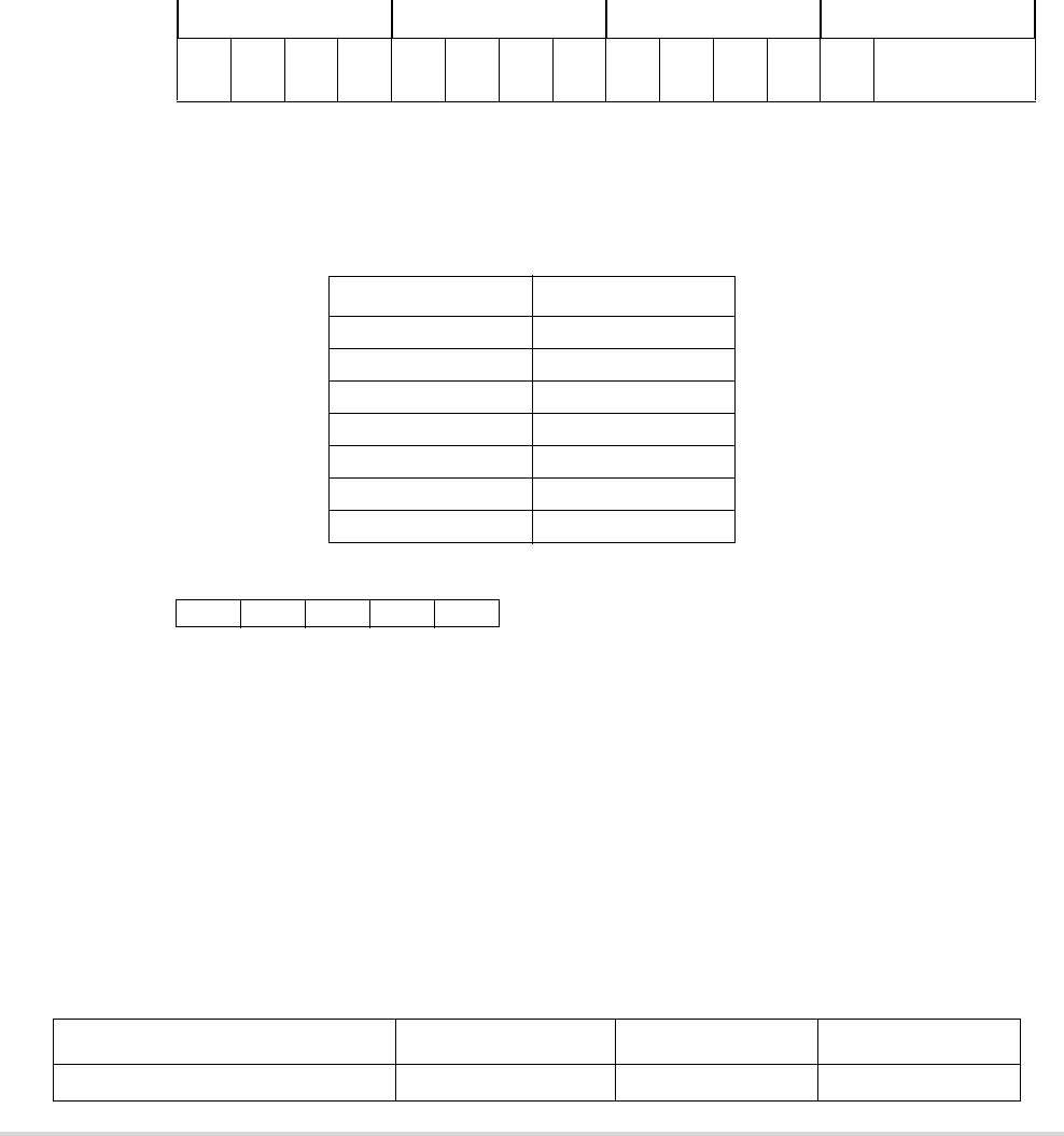
MOTOROLA Chapter 2. ColdFire Core 2-31
ColdFire Instruction Set Architecture Enhancements
FF1 Find First One in Register FF1
(Supported Starting with ISA A+)
Operation: Bit Offset of the First Logical One in Register → Destination
Assembler Syntax: FF1.L Dx
Attributes: Size = longword
The data register, Dx, is scanned, beginning from the most-significant bit (Dx[31]) and
ending with the least-significant bit (Dx[0]), searching for the first set bit. The data register
is then loaded with the offset count from bit 31 where the first set bit appears, as shown
below. If the source data is zero, then an offset of 32 is returned.
Instruction Field:
• Destination Register field—Specifies the destination data register, Dx.
Instruction
Format:
1514131211109876543210
0000010011000 Destination
Register, Dx
Old Dx[31:0] New Dx[31:0]
0b1---- . . . ---- 0x0000 0000
0b01--- . . . ---- 0x0000 0001
0b001-- . . . ---- 0x0000 0002
... ...
0b00000 . . . 0010 0x0000 001E
0b00000 . . . 0001 0x0000 001F
0b00000 . . . 0000 0x0000 0020
Condition
Codes:
X N Z V C X Not affected
N Set if the msb of the source operand is set; cleared
otherwise
Z Set if the source operand is zero; cleared otherwise
V Always cleared
C Always cleared
—∗∗00
FF1 V2, V3 Core (ISA_A) V4 Core (ISA_B) V2 Core (ISA_A+)
Opcode present No No Yes

2-32 MCF5282 User’s Manual MOTOROLA
ColdFire Instruction Set Architecture Enhancements
STRLDSR Store/Load Status Register STRLDSR
(Supported Starting with ISA A+)
Operation: If Supervisor State
Then SP - 4 → SP; zero-filled SR → (SP); immediate data → SR
Else TRAP
Assembler Syntax:STRLDSR #<data>
Attributes: Size = word
Description: Pushes the contents of the Status Register onto the stack and then reloads
the Status Register with the immediate data value. This instruction is intended for use as
the first instruction of an interrupt service routine shared across multiple interrupt request
levels. It allows the level of the just-taken interrupt request to be stored in memory (using
the SR[IML] field), and then masks interrupts by loading the SR[IML] field with 0x7 (if
desired). If execution is attempted with bit 13 of the immediate data cleared (attempting
to place the processor in user mode), a privilege violation exception is generated. The
opcode for STRLDSR is 0x40E7 46FC.
Instruction
Format:
1514131211109876543210
0100000011100111
0100011011111100
Immediate Data
Condition
Codes:
X N Z V C X Set to the value of bit 4 of the immediate operand
N Set to the value of bit 3 of the immediate operand
Z Set to the value of bit 2 of the immediate operand
V Set to the value of bit 1 of the immediate operand
C Set to the value of bit 0 of the immediate operand
∗∗∗∗∗
STRLDSR V2, V3 Core (ISA_A) V4 Core (ISA_B) V2 Core (ISA_A+)
Opcode present No No Yes

MOTOROLA Chapter 3. Enhanced Multiply-Accumulate Unit (EMAC) 3-1
Chapter 3
Enhanced Multiply-Accumulate Unit
(EMAC)
This chapter describes the functionality, microarchitecture, and performance of the
enhanced multiply-accumulate (EMAC) unit in the ColdFire family of processors.
3.1 Multiply-Accumulate Unit
The MAC design provides a set of DSP operations which can be used to improve the
performance of embedded code while supporting the integer multiply instructions of the
baseline ColdFire architecture.
The MAC provides functionality in three related areas:
• Signed and unsigned integer multiplies
• Multiply-accumulate operations supporting signed and unsigned integer operands as
well as signed, fixed-point, fractional operands
• Miscellaneous register operations
The ColdFire family supports two MAC implementations with different performance levels
and capabilities. The original MAC uses a three-stage execution pipeline optimized for
16-bit operands and featuring a 16x16 multiply array with a single 32-bit accumulator. The
EMAC features a four-stage pipeline optimized for 32-bit operands, with a fully pipelined
32x32 multiply array and four 48-bit accumulators.
The first ColdFire MAC supported signed and unsigned integer operands and was
optimized for 16x16 operations, such as those found in a variety of applications including
servo control and image compression. As ColdFire-based systems proliferated, the desire
for more precision on input operands increased. The result was an improved ColdFire MAC
with user-programmable control to optionally enable use of fractional input operands.
EMAC improvements target three primary areas:
• Improved performance of 32x32 multiply operations.
• Addition of three more accumulators to minimize MAC pipeline stalls caused by
exchanges between the accumulator and the pipeline’s general-purpose registers.
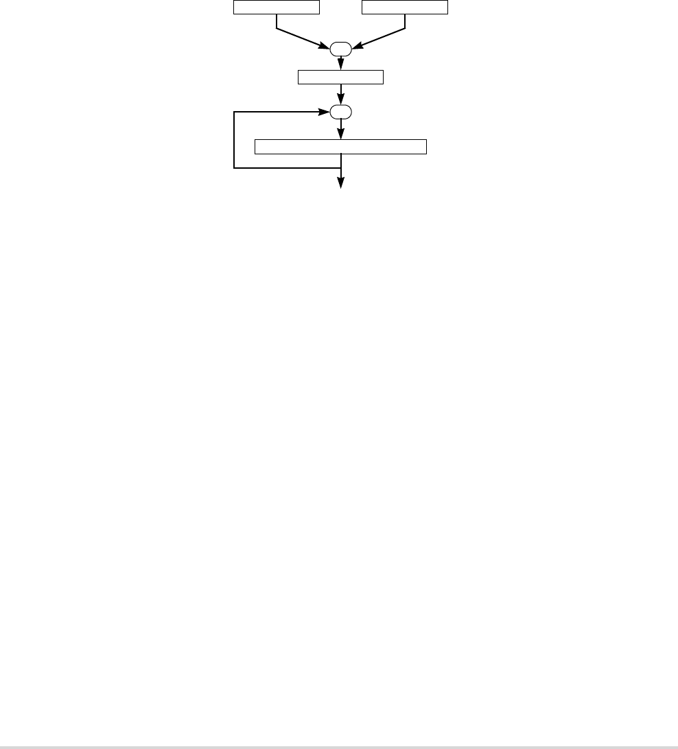
3-2 MCF5282 User’s Manual MOTOROLA
Introduction to the MAC
• A 48-bit accumulation data path to allow the use of a 40-bit product plus the addition
of 8 extension bits to increase the dynamic number range when implementing signal
processing algorithms.
The three areas of functionality are addressed in detail in following sections. The logic
required to support this functionality is contained in a MAC module, as shown in
Figure 3-1.
Figure 3-1. Multiply-Accumulate Functionality Diagram
3.2 Introduction to the MAC
The MAC is an extension of the basic multiplier found in most microprocessors. It is
typically implemented in hardware within an architecture and supports rapid execution of
signal processing algorithms in fewer cycles than comparable non-MAC architectures. For
example, small digital filters can tolerate some variance in an algorithm’s execution time,
but larger, more complicated algorithms such as orthogonal transforms may have more
demanding speed requirements beyond the scope of any processor architecture and may
require full DSP implementation.
To strike a balance between speed, size, and functionality, the ColdFire MAC is optimized
for a small set of operations that involve multiplication and cumulative additions.
Specifically, the multiplier array is optimized for single-cycle pipelined operations with a
possible accumulation after product generation. This functionality is common in many
signal processing applications. The ColdFire core architecture also has been modified to
allow an operand to be fetched in parallel with a multiply, increasing overall performance
for certain DSP operations.
Consider a typical filtering operation where the filter is defined as in Figure 3-2.
X
+/-
Operand Y Operand X
Shift 0,1,-1
Accumulator(s)

MOTOROLA Chapter 3. Enhanced Multiply-Accumulate Unit (EMAC) 3-3
General Operation
Figure 3-2. Infinite Impulse Response (IIR) Filter
Here, the output y(i) is determined by past output values and past input values. This is the
general form of an infinite impulse response (IIR) filter. A finite impulse response (FIR)
filter can be obtained by setting coefficients a(k) to zero. In either case, the operations
involved in computing such a filter are multiplies and product summing. To show this point,
reduce the above equation to a simple, four-tap FIR filter, shown in Figure 3-3, in which
the accumulated sum is a sum of past data values and coefficients.
Figure 3-3. Four-Tap FIR Filter
3.3 General Operation
The MAC speeds execution of ColdFire integer multiply instructions (MULS and MULU)
and provides additional functionality for multiply-accumulate operations. By executing
MULS and MULU in the MAC, execution times are minimized and deterministic
compared to the 2-bit/cycle algorithm with early termination that the OEP normally uses if
no MAC hardware is present.
The added MAC instructions to the ColdFire ISA provide for the multiplication of two
numbers, followed by the addition or subtraction of the product to or from the value in an
accumulator. Optionally, the product may be shifted left or right by 1 bit before addition or
subtraction. Hardware support for saturation arithmetic can be enabled to minimize
software overhead when dealing with potential overflow conditions. Multiply-accumulate
operations support 16- or 32-bit input operands of the following formats:
• Signed integers
• Unsigned integers
• Signed, fixed-point, fractional numbers
The EMAC is optimized for single-cycle, pipelined 32x32 multiplications. For word- and
longword-sized integer input operands, the low-order 40 bits of the product are formed and
used with the destination accumulator. For fractional operands, the entire 64-bit product is
calculated and either truncated or rounded to the most-significant 40-bit result using the
round-to-nearest (even) method before it is combined with the destination accumulator.
yi() a
k1=
N1–
∑
=k()yi k–() b
k0=
N1–
∑k()xi k–()+
yi() bk()xi k–()
k0=
3
∑b0()xi() b1()xi 1–()b2()xi 2–()b3()xi 3–()+++==
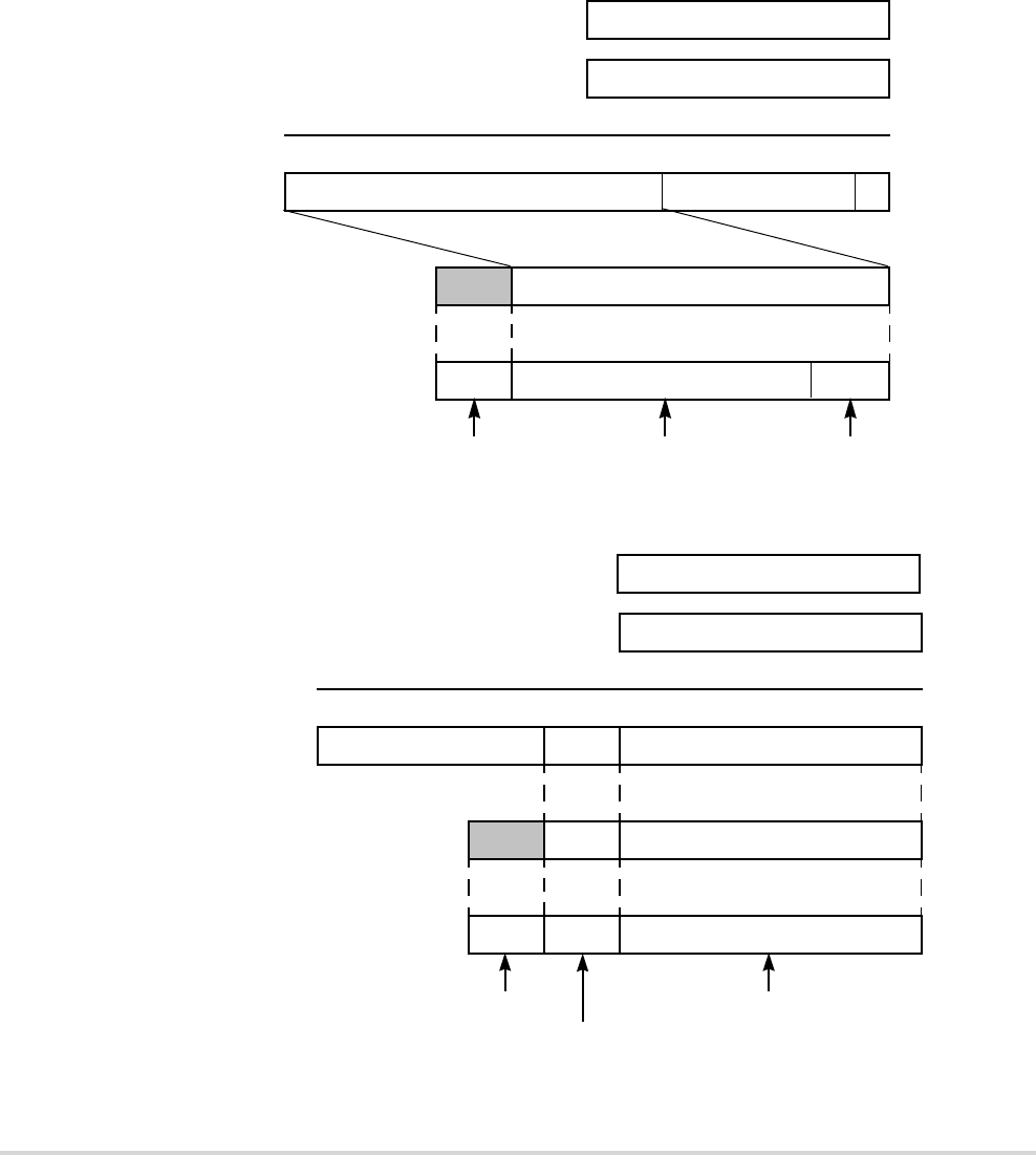
3-4 MCF5282 User’s Manual MOTOROLA
General Operation
For all operations, the resulting 40-bit product is extended to a 48-bit value (using
sign-extension for signed integer and fractional operands, zero-fill for unsigned integer
operands) before being combined with the 48-bit destination accumulator.
Figure 3-4 and Figure 3-5 show relative alignment of input operands, the full 64-bit
product, the resulting 40-bit product used for accumulation, and 48-bit accumulator
formats.
Figure 3-4. Fractional Alignment
Figure 3-5. Signed and Unsigned Integer Alignment
X
OperandY
OperandX
Product
Extended Product
Accumulator
32
8
Extension Byte Upper [7:0]
+
“0”
32
40 23
40
840 8
Accumulator [31:0] Extension Byte Lower [7:0]
X
OperandY
OperandX
Product
Extended Product
Accumulator
32
32
32
32
32
8
8
8
24
8
8
+
Extension Byte Upper [7:0]
Extension Byte Lower [7:0]
Accumulator [31:0]

MOTOROLA Chapter 3. Enhanced Multiply-Accumulate Unit (EMAC) 3-5
General Operation
Thus, the 48-bit accumulator definition is a function of the EMAC operating mode. Given
that each 48-bit accumulator is the concatenation of 16-bit accumulator extension register
(ACCextn) contents and 32-bit ACCn contents, the specific definitions are as follows:
if MACSR[6:5] == 00/* signed integer mode */
Complete Accumulator[47:0] = {ACCextn[15:0], ACCn[31:0]}
if MACSR[6:5] == -1/* signed fractional mode */
Complete Accumulator [47:0] = {ACCextn[15:8], ACCn[31:0], ACCextn[7:0]}
if MACSR[6:5] == 10/* unsigned integer mode */
Complete Accumulator[47:0] = {ACCextn[15:0], ACCn[31:0]}
The four accumulators are represented as an array, ACCn, where n selects the register.
Although the multiplier array is implemented in a four-stage pipeline, all arithmetic MAC
instructions have an effective issue rate of 1 cycle, regardless of input operand size or type.
All arithmetic operations use register-based input operands, and summed values are stored
internally in an accumulator. Thus, an additional move instruction is needed to store data in
a general-purpose register. One new feature found in EMAC instructions is the ability to
choose the upper or lower word of a register as a 16-bit input operand. This is useful in
filtering operations if one data register is loaded with the input data and another is loaded
with the coefficient. Two 16-bit multiply accumulates can be performed without fetching
additional operands between instructions by alternating the word choice during the
calculations.
The EMAC has four accumulator registers versus the MAC’s single accumulator. The
additional registers improve the performance of some algorithms by minimizing pipeline
stalls needed to store an accumulator value back to general-purpose registers. Many
algorithms require multiple calculations on a given data set. By applying different
accumulators to these calculations, it is often possible to store one accumulator without any
stalls while performing operations involving a different destination accumulator.
The need to move large amounts of data presents an obstacle to obtaining high throughput
rates in DSP engines. New and existing ColdFire instructions can accommodate these
requirements. A MOVEM instruction can move large blocks of data efficiently by
generating line-sized burst references. The ability to simultaneously load an operand from
memory into a register and execute a MAC instruction makes some DSP operations such
as filtering and convolution more manageable.
The programming model includes a 16-bit mask register (MASK), which can optionally be
used to generate an operand address during MAC + MOVE instructions. The application of
this register with auto-increment addressing mode supports efficient implementation of
circular data queues for memory operands.
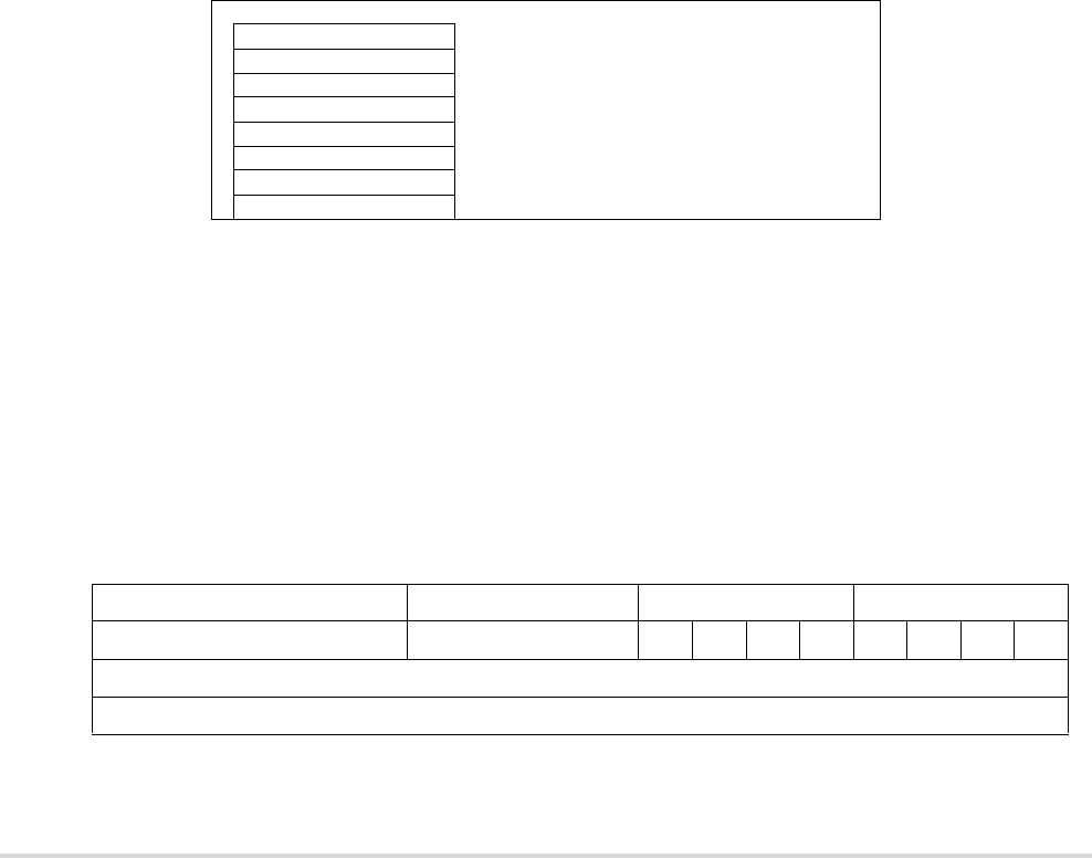
3-6 MCF5282 User’s Manual MOTOROLA
Memory Map/Register Set
The additional MAC status register (MACSR) contains a 4-bit operational mode field and
condition flags. Operational mode bits control whether operands are signed or unsigned and
whether they are treated as integers or fractions. These bits also control the
overflow/saturation mode and the way in which rounding is performed. Negative, zero, and
multiple overflow condition flags are also provided.
3.4 Memory Map/Register Set
The EMAC provides the following program-visible registers:
• Four 32-bit accumulators (ACCn = ACC0, ACC1, ACC2, and ACC3)
• Eight 8-bit accumulator extensions (two per accumulator), packaged as two 32-bit
values for load and store operations (ACCext01 and ACCext23)
• One 16-bit mask register (MASK)
• One 32-bit MAC status register (MACSR) including four indicator bits signaling
product or accumulation overflow (one for each accumulator: PAV0–PAV3)
These registers are shown in Figure 3-6.
Figure 3-6. EMAC Register Set
3.4.1 MAC Status Register (MACSR)
MACSR functionality is organized as follows:
• MACSR[11–8] contains one product/accumulation overflow flag per accumulator.
• MACSR[7–4] defines the operating configuration of the MAC unit.
• MACSR[3–0] contains indicator flags from the last MAC instruction execution.
Table 3-1 describes MACSR fields.
31 0
MACSR MAC status register
ACC0 MAC accumulator 0
ACC1 MAC accumulator 1
ACC2 MAC accumulator 2
ACC3 MAC accumulator 3
ACCext01 Extensions for ACC0 and ACC1
ACCext23 Extensions for ACC2 and ACC3
MASK MAC mask register
Bit31 12 11–8 76543210
Prod/acc overflow flags Operational Mode Flags
Field — PAVx OMC S/U F/I R/T N Z V EV
Reset 0000_0000_0000_0000_0000_0000_0000_0000
R/W R/W
Figure 3-7. MAC Status Register (MACSR)

MOTOROLA Chapter 3. Enhanced Multiply-Accumulate Unit (EMAC) 3-7
Memory Map/Register Set
Table 3-1. MACSR Field Descriptions
Bits Name Description
31–12 — Reserved, should be cleared.
11–8 PAVxProduct/accumulation overflow flags. Contains four flags, one per accumulator, that indicate if past
MAC or MSAC instructions generated an overflow during product calculation or the 48-bit
accumulation. When a MAC or MSAC instruction is executed, the PAVx flag associated with the
destination accumulator is used to form the general overflow flag, MACSR[V]. Once set, each flag
remains set until V is cleared by a MOV.L , MACSR instruction or the accumulator is loaded
directly.
7–4 Operational Mode Fields
7 OMC Overflow/saturation mode. Used to enable or disable saturation mode on overflow. If set, the
accumulator is set to the appropriate constant on any operation which overflows the accumulator.
Once saturated, the accumulator remains unaffected by any other MAC or MSAC instructions until
either the overflow bit is cleared or the accumulator is directly loaded.
6 S/U Signed/unsigned operations.
In integer mode:
S/U determines whether operations performed are signed or unsigned. It also determines the
accumulator value during saturation, if enabled.
0 Signed numbers. On overflow, if OMC is enabled, an accumulator saturates to the most positive
(0x7FFF_FFFF) or the most negative (0x8000_0000) number, depending on both the instruction
and the value of the product that overflowed.
1 Unsigned numbers. On overflow, if OMC is enabled, an accumulator saturates to the smallest
value (0x0000_0000) or the largest value (0xFFFF_FFFF), depending on the instruction.
In fractional mode:
S/U controls rounding while storing an accumulator to a general-purpose register.
0 Move accumulator without rounding to a 16-bit value. Accumulator is moved to a
general-purpose register as a 32-bit value.
1 The accumulator is rounded to a 16-bit value using the round-to-nearest (even) method when it
is moved to a general-purpose register. See Section 3.4.1.1.1, “Rounding.” The resulting 16-bit
value is stored in the lower word of the destination register. The upper word is zero-filled. The
accumulator value is not affected by this rounding procedure.
5 F/I Fractional/integer mode Determines whether input operands are treated as fractions or integers.
0 Integers can be represented in either signed or unsigned notation, depending on the value of S/U.
1 Fractions are represented in signed, fixed-point, two’s complement notation. Values range from
-1 to 1- 2-15 for 16-bit fractions and -1 to 1 - 2-31 for 32-bit fractions. See Section 3.5.2, “Data
Representation."
4 R/T Round/truncate mode. Controls the rounding procedure for MOV.L ACCx,Rx, or MSAC.L
instructions when operating in fractional mode.
0 Truncate. The product’s lsbs are dropped before it is combined with the accumulator.
Additionally, when a store accumulator instruction is executed (MOV.L ACCx,Rx), the 8 lsbs of
the 48-bit accumulator logic are simply truncated.
1 Round-to-nearest (even). The 64-bit product of two 32-bit, fractional operands is rounded to the
nearest 40-bit value. If the low-order 24 bits equal 0x80_0000, the upper 40 bits are rounded to
the nearest even (lsb = 0) value.See Section 3.4.1.1.1, “Rounding.” Additionally, when a store
accumulator instruction is executed (MOV.L ACCx,Rx), the lsbs of the 48-bit accumulator logic
are used to round the resulting 16- or 32-bit value. If MACSR[S/U] = 0 and MACSR[R/T] = 1,
the low-order 8 bits are used to round the resulting 32-bit fraction. If MACSR[S/U] = 1, the
low-order 24 bits are used to round the resulting 16-bit fraction.
3–0 Flags
3 N Negative. Set if the msb of the result is set, otherwise cleared. N is affected only by MAC, MSAC,
and load operations; it is not affected by MULS and MULU instructions.

3-8 MCF5282 User’s Manual MOTOROLA
Memory Map/Register Set
Table 3-2 summarizes the interaction of the MACSR[S/U,F/I,R/T] control bits.
3.4.1.1 Fractional Operation Mode
This section describes behavior when the fractional mode is used (MACSR[F/I] is set).
3.4.1.1.1 Rounding
When the processor is in fractional mode, there are two operations during which rounding
can occur.
• Execution of a store accumulator instruction (MOV.L ACCx,Rx). The lsbs of the
48-bit accumulator logic are used to round the resulting 16- or 32-bit value. If
MACSR[S/U] is cleared, the low-order 8 bits are used to round the resulting 32-bit
fraction. If MACSR[S/U] is set, the low-order 24 bits are used to round the resulting
16-bit fraction.
2 Z Zero. Set if the result equals zero, otherwise cleared. This bit is affected only by MAC, MSAC, and
load operations; it is not affected by MULS and MULU instructions.
1 V Overflow. Set if an arithmetic overflow occurs on a MAC or MSAC instruction indicating that the
result cannot be represented in the limited width of the EMAC. V is set only if a product overflow
occurs or the accumulation overflows the 48-bit structure. V is evaluated on each MAC or MSAC
operation and uses the appropriate PAVx flag in the next-state V evaluation.
0 EV Extension overflow. Signals that the last MAC or MSAC instruction overflowed the 32 lsbs in
integer mode or the 40 lsbs in fractional mode of the destination accumulator. However, the result is
still accurately represented in the combined 48-bit accumulator structure. Although an overflow has
occurred, the correct result, sign, and magnitude are contained in the 48-bit accumulator. Subsequent
MAC or MSAC operations may return the accumulator to a valid 32/40-bit result.
Table 3-2. Summary of S/U, F/I, and R/T Control Bits
S/U F/I R/T Operational Modes
0 0 x Signed, integer
0 1 0 Signed, fractional
Truncate on MAC.L and MSAC.L
No round on accumulator stores
0 1 1 Signed, fractional
Round on MAC.L and MSAC.L
Round-to-32-bits on accumulator stores
1 0 x Unsigned, integer
1 1 0 Signed, fractional
Truncate on MAC.L and MSAC.L
Round-to-16-bits on accumulator stores
1 1 1 Signed, fractional
Round on MAC.L and MSAC.L
Round-to-16-bits on accumulator stores
Table 3-1. MACSR Field Descriptions (continued)
Bits Name Description

MOTOROLA Chapter 3. Enhanced Multiply-Accumulate Unit (EMAC) 3-9
Memory Map/Register Set
• Execution of a MAC (or MSAC) instruction with 32-bit operands. If MACSR[R/T]
is zero, multiplying two 32-bit numbers creates a 64-bit product that is truncated to
the upper 40 bits; otherwise, it is rounded using round-to-nearest (even) method.
To understand the round-to-nearest-even method, consider the following example
involving the rounding of a 32-bit number, R0, to a 16-bit number. Using this method, the
32-bit number is rounded to the closest 16-bit number possible. Let the high-order 16 bits
of R0 be named R0.U and the low-order 16 bits be R0.L.
• If R0.L is less than 0x8000, the result is truncated to the value of R0.U.
• If R0.L is greater than 0x8000, the upper word is incremented (rounded up).
• If R0.L is 0x8000, R0 is half-way between two 16-bit numbers. In this case,
rounding is based on the lsb of R0.U, so the result is always even (lsb = 0).
— If the lsb of R0.U = 1 and R0.L = 0x8000, the number is rounded up.
— If the lsb of R0.U = 0 and R0.L =0x8000, the number is rounded down.
This method minimizes rounding bias and creates as statistically correct an answer as
possible.
The rounding algorithm is summarized in the following pseudocode:
if R0.L < 0x8000
then Result = R0.U
else if R0.L > 0x8000
then Result = R0.U + 1
else if lsb of R0.U = 0 /* R0.L = 0x8000 */
then Result = R0.U
else Result = R0.U + 1
The round-to-nearest-even technique is also known as convergent rounding.
3.4.1.1.2 Saving and Restoring the EMAC Programming Model
The presence of rounding logic in the output datapath of the EMAC requires that special
care be taken during the EMAC’s save/restore process. In particular, any result rounding
modes must be disabled during the save/restore process so the exact bit-wise contents of the
EMAC registers are accessed. Consider the following memory structure containing the
EMAC programming model:
struct macState {
int acc0;
int acc1;
int acc2;
int acc3;
int accext01;
int accext02;
int mask;
int macsr;
} macState;

3-10 MCF5282 User’s Manual MOTOROLA
Memory Map/Register Set
The following assembly language routine shows the proper sequence for a correct EMAC
state save. This code assumes all Dn and An registers are available for use and the memory
location of the state save is defined by A7.
EMAC_state_save:
move.l macsr,d7 ; save the macsr
clr.l d0 ; zero the register to ...
move.l d0,macsr ; disable rounding in the macsr
move.l acc0,d0 ; save the accumulators
move.l acc1,d1
move.l acc2,d2
move.l acc3,d3
move.l accext01,d4 ; save the accumulator extensions
move.l accext23,d5
move.l mask,d6 ; save the address mask
movem.l #0x00ff,(a7) ; move the state to memory
The following code performs the EMAC state restore:
EMAC_state_restore:
movem.l (a7),#0x00ff ; restore the state from memory
move.l #0,macsr ; disable rounding in the macsr
move.l d0,acc0 ; restore the accumulators
move.l d1,acc1
move.l d2,acc2
move.l d3,acc3
move.l d4,accext01 ; restore the accumulator extensions
move.l d5,accext23
move.l d6,mask ; restore the address mask
move.l d7,macsr ; restore the macsr
By executing this type of sequence, the exact state of the EMAC programming model can
be correctly saved and restored.
3.4.1.1.3 MULS/MULU
MULS and MULU are unaffected by fractional mode operation; operands are still assumed
to be integers.
3.4.1.1.4 Scale Factor in MAC or MSAC Instructions
The scale factor is ignored while the MAC is in fractional mode.
3.4.2 Mask Register (MASK)
The 32-bit MASK implements the low-order 16 bits to minimize the alignment
complications involved with loading and storing only 16 bits. When the MASK is loaded,
the low-order 16 bits of the source operand are actually loaded into the register. When it is
stored, the upper 16 bits are all forced to ones.

MOTOROLA Chapter 3. Enhanced Multiply-Accumulate Unit (EMAC) 3-11
Memory Map/Register Set
This register performs a simple AND with the operand address for MAC instructions. That
is, the processor calculates the normal operand address and, if enabled, that address is then
ANDed with {0xFFFF, MASK[15:0]} to form the final address. Therefore, with certain
MASK bits cleared, the operand address can be constrained to a certain memory region.
This is used primarily to implement circular queues in conjunction with the (An)+
addressing mode.
This feature minimizes the addressing support required for filtering, convolution, or any
routine that implements a data array as a circular queue. For MAC + MOVE operations, the
MASK contents can optionally be included in all memory effective address calculations.
The syntax is as follows:
MAC.sz Ry,RxSF,<ea>y&,Rw
The & operator enables the use of MASK and causes bit 5 of the extension word to be set.
The exact algorithm for the use of MASK is as follows:
if extension word, bit [5] = 1, the MASK bit, then
if <ea> = (An)
oa = An & {0xFFFF, MASK}
if <ea> = (An)+
oa = An
An = (An + 4) & {0xFFFF, MASK}
if <ea> =-(An)
oa = (An - 4) & {0xFFFF, MASK}
An = (An - 4) & {0xFFFF, MASK}
if <ea> = (d16,An)
oa = (An + se_d16) & {0xFFFF0x, MASK}
Here, oa is the calculated operand address and se_d16 is a sign-extended 16-bit
displacement. For auto-addressing modes of post-increment and pre-decrement, the
calculation of the updated An value is also shown.
Use of the post-increment addressing mode, {(An)+} with the MASK is suggested for
circular queue implementations.

3-12 MCF5282 User’s Manual MOTOROLA
EMAC Instruction Set Summary
3.5 EMAC Instruction Set Summary
Table 3-3 summarizes EMAC unit instructions.
3.5.1 EMAC Instruction Execution Times
The instruction execution times for the EMAC can be found in Section 2.12, “EMAC
Instruction Execution Times.”
The EMAC execution pipeline overlaps the AGEX stage of the OEP; that is, the first stage
of the EMAC pipeline is the last stage of the basic OEP. EMAC units are designed for
sustained, fully-pipelined operation on accumulator load, copy, and multiply-accumulate
instructions. However, instructions that store contents of the multiply-accumulate
programming model can generate OEP stalls that expose the EMAC execution pipeline
depth, as in the following:
mac.w Ry, Rx, Acc0
mov.l Acc0, Rz
Table 3-3. EMAC Instruction Summary
Command Mnemonic Description
Multiply Signed MULS <ea>y,Dx Multiplies two signed operands yielding a signed result
Multiply Unsigned MULU <ea>y,Dx Multiplies two unsigned operands yielding an unsigned result
Multiply Accumulate MAC Ry,RxSF,ACCx
MSAC Ry,RxSF,ACCx
Multiplies two operands and adds/subtracts the product to/from an
accumulator
Multiply Accumulate
with Load
MAC Ry,Rx,<ea>y,Rw,ACCx
MSAC Ry,Rx,<ea>y,Rw,ACCx
Multiplies two operands and combines the product to an
accumulator while loading a register with the memory operand
Load Accumulator MOV.L {Ry,#imm},ACCx Loads an accumulator with a 32-bit operand
Store Accumulator MOV.L ACCx,Rx Writes the contents of an accumulator to a CPU register
Copy Accumulator MOV.L ACCy,ACCx Copies a 48-bit accumulator
Load MACSR MOV.L {Ry,#imm},MACSR Writes a value to MACSR
Store MACSR MOV.L MACSR,Rx Write the contents of MACSR to a CPU register
Store MACSR to CCR MOV.L MACSR,CCR Write the contents of MACSR to the CCR
Load MAC Mask Reg MOV.L {Ry,#imm},MASK Writes a value to the MASK register
Store MAC Mask Reg MOV.L MASK,Rx Writes the contents of the MASK to a CPU register
Load AccExtensions01 MOV.L {Ry,#imm},ACCext01 Loads the accumulator 0,1 extension bytes with a 32-bit operand
Load AccExtensions23 MOV.L {Ry,#imm},ACCext23 Loads the accumulator 2,3 extension bytes with a 32-bit operand
Store AccExtensions01 MOV.L ACCext01,Rx Writes the contents of accumulator 0,1 extension bytes into a CPU
register
Store AccExtensions23 MOV.L ACCext23,Rx Writes the contents of accumulator 2,3 extension bytes into a CPU
register
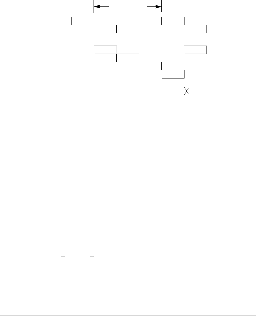
MOTOROLA Chapter 3. Enhanced Multiply-Accumulate Unit (EMAC) 3-13
EMAC Instruction Set Summary
The mov.l instruction that stores the accumulator to an integer register (Rz) stalls until the
program-visible copy of the accumulator is available. Figure 3-8 shows EMAC timing.
Figure 3-8. EMAC-Specific OEP Sequence Stall
In Figure 3-8, the OEP stalls the store-accumulator instruction for 3 cycles: the depth of the
EMAC pipeline minus 1. The minus 1 factor is needed because the OEP and EMAC
pipelines overlap by a cycle, the AGEX stage. As the store-accumulator instruction reaches
the AGEX stage where the operation is performed, the just-updated accumulator 0 value is
available.
As with change or use stalls between accumulators and general-purpose registers,
introducing intervening instructions that do not reference the busy register can reduce or
eliminate sequence-related store-MAC instruction stalls. In fact, a major benefit of the
EMAC is the addition of three accumulators to minimize stalls caused by exchanges
between the accumulator(s) and the general-purpose registers.
3.5.2 Data Representation
MACSR[S/U,F/I] selects one of the following three modes, where each mode defines a
unique operand type.
• Two’s complement signed integer: In this format, an N-bit operand value lies in the
range -2(N-1) < operand < 2(N-1) - 1. The binary point is right of the lsb.
• Unsigned integer: In this format, an N-bit operand value lies in the range 0 < operand
< 2N - 1. The binary point is right of the lsb.
• Two’s complement, signed fractional: In an N-bit number, the first bit is the sign bit.
The remaining bits signify the first N-1 bits after the binary point. Given an N-bit
number, aN-1aN-2aN-3... a2a1a0, its value is given by the equation in Figure 3-9.
DSOC
AGEX
mac
mac
EMAC EX1
EMAC EX2
EMAC EX3
EMAC EX4
mac
mac
mac
mac
mov
mov
mov
mov
Three-cycle
regBusy stall
Accumulator 0 old new

3-14 MCF5282 User’s Manual MOTOROLA
EMAC Instruction Set Summary
Figure 3-9. Two’s Complement, Signed Fractional Equation
This format can represent numbers in the range -1 < operand < 1 - 2(N-1).
For words and longwords, the largest negative number that can be represented is -1, whose
internal representation is 0x8000 and 0x8000_0000, respectively. The largest positive word
is 0x7FFF or (1 - 2-15); the most positive longword is 0x7FFF_FFFF or (1 - 2-31).
3.5.3 MAC Opcodes
MAC opcodes are described in the ColdFire Programmer’s Reference Manual.
Note the following:
• Unless otherwise noted, the value of MACSR[N,Z] is based on the result of the final
operation that involves the product and the accumulator.
• The overflow (V) flag is handled differently. It is set if the complete product cannot
be represented as a 40-bit value (this applies to 32x32 integer operations only) or if
the combination of the product with an accumulator cannot be represented in the
given number of bits. The EMAC design includes an additional
product/accumulation overflow bit for each accumulator that are treated as sticky
indicators and are used to calculate the V bit on each MAC or MSAC instruction.
See Section 3.4.1, “MAC Status Register (MACSR).”
• For the MAC design, the assembler syntax of the MAC (multiply and add to
accumulator) and MSAC (multiply and subtract from accumulator) instructions
does not include a reference to the single accumulator. For the EMAC, it is expected
that assemblers support this syntax and that no explicit reference to an accumulator
is interpreted as a reference to ACC0. These assemblers would also support syntaxes
where the destination accumulator is explicitly defined.
• The optional 1-bit shift of the product is specified using the notation {<< | >>} SF,
where <<1 indicates a left shift and >>1 indicates a right shift. The shift is performed
before the product is added to or subtracted from the accumulator. Without this
operator, the product is not shifted. If the EMAC is in fractional mode (MACSR[F/I]
is set), SF is ignored and no shift is performed. Because a product can overflow, the
following guidelines are implemented:
value 1 aN1–
⋅()–2
i1N–+()
ai⋅
i0=
N2–
∑
+=

MOTOROLA Chapter 3. Enhanced Multiply-Accumulate Unit (EMAC) 3-15
EMAC Instruction Set Summary
— For unsigned word and longword operations, a zero is shifted into the product on
right shifts.
— For signed, word operations, the sign bit is shifted into the product on right shifts
unless the product is zero. For signed, longword operations, the sign bit is shifted
into the product unless an overflow occurs or the product is zero, in which case
a zero is shifted in.
— For all left shifts, a zero is inserted into the lsb position.
The following pseudocode explains basic MAC or MSAC instruction functionality. This
example is presented as a case statement covering the three basic operating modes with
signed integers, unsigned integers, and signed fractionals. Throughout this example, a
comma-separated list in curly brackets, {}, indicates a concatenation operation.
switch (MACSR[6:5]) /* MACSR[S/U, F/I] */
{
case 0: /* signed integers */
if (MACSR.OMC == 0 || MACSR.PAVx == 0)
then {
MACSR.PAVx = 0
/* select the input operands */
if (sz == word)
then {if (U/Ly == 1)
then operandY[31:0] = {sign-extended Ry[31], Ry[31:16]}
else operandY[31:0] = {sign-extended Ry[15], Ry[15:0]}
if (U/Lx == 1)
then operandX[31:0] = {sign-extended Rx[31], Rx[31:16]}
else operandX[31:0] = {sign-extended Rx[15], Rx[15:0]}
}
else {operandY[31:0] = Ry[31:0]
operandX[31:0] = Rx[31:0]
}
/* perform the multiply */
product[63:0] = operandY[31:0] * operandX[31:0]
/* check for product overflow */
if ((product[63:39] != 0x0000_00_0) && (product[63:39] != 0xffff_ff_1))
then { /* product overflow */
MACSR.PAVx = 1
MACSR.V = 1
if (inst == MSAC && MACSR.OMC == 1)
then if (product[63] == 1)
then result[47:0] = 0x0000_7fff_ffff
else result[47:0] = 0xffff_8000_0000
else if (MACSR.OMC == 1)
then /* overflowed MAC,
saturationMode enabled */
if (product[63] == 1)
then result[47:0] = 0xffff_8000_000
0
else result[47:0] = 0x0000_7fff_fff

3-16 MCF5282 User’s Manual MOTOROLA
EMAC Instruction Set Summary
f
}
/* sign-extend to 48 bits before performing any scaling */
product[47:40] = {8{product[39]}} /* sign-extend */
/* scale product before combining with accumulator */
switch (SF) /* 2-bit scale factor */
{
case 0: /* no scaling specified */
break;
case 1: /* SF = “<< 1” */
product[40:0] = {product[39:0], 0}
break;
case 2: /* reserved encoding */
break;
case 3: /* SF = “>> 1” */
product[39:0] = {product[39], product[39:1]}
break;
}
if (MACSR.PAVx == 0)
then {if (inst == MSAC)
then result[47:0] = ACCx[47:0] - product[47:0]
else result[47:0] = ACCx[47:0] + product[47:0]
}
/* check for accumulation overflow */
if (accumulationOverflow == 1)
then {MACSR.PAVx = 1
MACSR.V = 1
if (MACSR.OMC == 1)
then /* accumulation overflow,
saturationMode enabled */
if (result[47] == 1)
then result[47:0] = 0x0000_7fff_ffff
else result[47:0] = 0xffff_8000_0000
}
/* transfer the result to the accumulator */
ACCx[47:0] = result[47:0]
}
MACSR.V = MACSR.PAVx
MACSR.N = ACCx[47]
if (ACCx[47:0] == 0x0000_0000_0000)
then MACSR.Z = 1
else MACSR.Z = 0
if ((ACCx[47:31] == 0x0000_0) || (ACCx[47:31] == 0xffff_1))
then MACSR.EV = 0
else MACSR.EV = 1
break;
case 1,3: /* signed fractionals */
if (MACSR.OMC == 0 || MACSR.PAVx == 0)
then {
MACSR.PAVx = 0

MOTOROLA Chapter 3. Enhanced Multiply-Accumulate Unit (EMAC) 3-17
EMAC Instruction Set Summary
if (sz == word)
then {if (U/Ly == 1)
then operandY[31:0] = {Ry[31:16], 0x0000}
else operandY[31:0] = {Ry[15:0], 0x0000}
if (U/Lx == 1)
then operandX[31:0] = {Rx[31:16], 0x0000}
else operandX[31:0] = {Rx[15:0], 0x0000}
}
else {operandY[31:0] = Ry[31:0]
operandX[31:0] = Rx[31:0]
}
/* perform the multiply */
product[63:0] = (operandY[31:0] * operandX[31:0]) << 1
/* check for product rounding */
if (MACSR.R/T == 1)
then { /* perform convergent rounding */
if (product[23:0] > 0x80_0000)
then product[63:24] = product[63:24] + 1
else if ((product[23:0] == 0x80_0000) && (product[24] == 1))
then product[63:24] = product[63:24] + 1
}
/* sign-extend to 48 bits and combine with accumulator */
/* check for the -1 * -1 overflow case */
if ((operandY[31:0] == 0x8000_0000) && (operandX[31:0] == 0x8000_0000))
then product[71:64] = 0x00 /* zero-fill */
else product[71:64] = {8{product[63]}} /* sign-extend */
if (inst == MSAC)
then result[47:0] = ACCx[47:0] - product[71:24]
else result[47:0] = ACCx[47:0] + product[71:24]
/* check for accumulation overflow */
if (accumulationOverflow == 1)
then {MACSR.PAVx = 1
MACSR.V = 1
if (MACSR.OMC == 1)
then /* accumulation overflow,
saturationMode enabled */
if (result[47] == 1)
then result[47:0] = 0x007f_ffff_ff00
else result[47:0] = 0xff80_0000_0000
}
/* transfer the result to the accumulator */
ACCx[47:0] = result[47:0]
}
MACSR.V = MACSR.PAVx
MACSR.N = ACCx[47]
if (ACCx[47:0] == 0x0000_0000_0000)
then MACSR.Z = 1
else MACSR.Z = 0
if ((ACCx[47:39] == 0x00_0) || (ACCx[47:39] == 0xff_1))
then MACSR.EV = 0
else MACSR.EV = 1
break;
case 2: /* unsigned integers */
if (MACSR.OMC == 0 || MACSR.PAVx == 0)

3-18 MCF5282 User’s Manual MOTOROLA
EMAC Instruction Set Summary
then {
MACSR.PAVx = 0
/* select the input operands */
if (sz == word)
then {if (U/Ly == 1)
then operandY[31:0] = {0x0000, Ry[31:16]}
else operandY[31:0] = {0x0000, Ry[15:0]}
if (U/Lx == 1)
then operandX[31:0] = {0x0000, Rx[31:16]}
else operandX[31:0] = {0x0000, Rx[15:0]}
}
else {operandY[31:0] = Ry[31:0]
operandX[31:0] = Rx[31:0]
}
/* perform the multiply */
product[63:0] = operandY[31:0] * operandX[31:0]
/* check for product overflow */
if (product[63:40] != 0x0000_00)
then { /* product overflow */
MACSR.PAVx = 1
MACSR.V = 1
if (inst == MSAC && MACSR.OMC == 1)
then result[47:0] = 0x0000_0000_0000
else if (MACSR.OMC == 1)
then /* overflowed MAC,
saturationMode enabled */
result[47:0] = 0xffff_ffff_ffff
}
/* zero-fill to 48 bits before performing any scaling */
product[47:40] = 0 /* zero-fill upper byte */
/* scale product before combining with accumulator */
switch (SF) /* 2-bit scale factor */
{
case 0: /* no scaling specified */
break;
case 1: /* SF = “<< 1” */
product[40:0] = {product[39:0], 0}
break;
case 2: /* reserved encoding */
break;
case 3: /* SF = “>> 1” */
product[39:0] = {0, product[39:1]}
break;
}
/* combine with accumulator */
if (MACSR.PAVx == 0)
then {if (inst == MSAC)
then result[47:0] = ACCx[47:0] - product[47:0]
else result[47:0] = ACCx[47:0] + product[47:0]

MOTOROLA Chapter 3. Enhanced Multiply-Accumulate Unit (EMAC) 3-19
EMAC Instruction Set Summary
}
/* check for accumulation overflow */
if (accumulationOverflow == 1)
then {MACSR.PAVx = 1
MACSR.V = 1
if (inst == MSAC && MACSR.OMC == 1)
then result[47:0] = 0x0000_0000_0000
else if (MACSR.OMC == 1)
then /* overflowed MAC,
saturationMode enabled */
result[47:0] = 0xffff_ffff_ffff
}
/* transfer the result to the accumulator */
ACCx[47:0] = result[47:0]
}
MACSR.V = MACSR.PAVx
MACSR.N = ACCx[47]
if (ACCx[47:0] == 0x0000_0000_0000)
then MACSR.Z = 1
else MACSR.Z = 0
if (ACCx[47:32] == 0x0000)
then MACSR.EV = 0
else MACSR.EV = 1
break;
}

3-20 MCF5282 User’s Manual MOTOROLA
EMAC Instruction Set Summary

MOTOROLA Chapter 4. Cache 4-1
Chapter 4
Cache
This chapter describes the MCF5282 cache operation.
4.1 Cache Features
• Configurable as instruction, data, or split instruction/data cache
• 2-Kbyte direct-mapped cache
• Single-cycle access on cache hits
• Physically located on the Coldfire core's high-speed local bus
• Nonblocking design to maximize performance
• Separate instruction and data 16-Byte line-fill buffers
• Configurable instruction cache miss-fetch algorithm
4.2 Cache Physical Organization
The cache is a direct-mapped single-cycle memory. It may be configured as an instruction
cache, a write-through data cache, or a split instruction/data cache. The cache storage is
organized as 128 lines, each containing 16 bytes. The memory storage consists of a
128-entry tag array (containing addresses and a valid bit), and a data array containing 2
Kbytes, organized as 512 x 32 bits.
Cache configuration is controlled by bits in the cache control register (CACR) that is
detailed later in this chapter. For the instruction or data-only configurations, only the
associated instruction or data line-fill buffer is used. For the split cache configuration,
one-half of the tag and storage arrays is used for an instruction cache and one-half is used
for a data cache. The split cache configuration uses both the instruction and the data line-fill
buffers. The core’s local bus is a unified bus used for both instruction and data fetches.
Therefore, the cache can have only one fetch, either instruction or data, active at one time.
For the instruction- or data-only configurations, the cache tag and storage arrays are
accessed in parallel: fetch address bits [10:4] addressing the tag array and fetch address bits
[10:2] addressing the storage array. For the split cache configuration, the cache tag and
storage arrays are accessed in parallel. The msb of the tag array address is set for instruction
fetches and cleared for operand fetches; fetch address bits [9:4] provide the rest of the tag

4-2 MCF5282 User’s Manual MOTOROLA
Cache Physical Organization
array address. The tag array outputs the address mapped to the given cache location along
with the valid bit for the line. This address field is compared to bits [31:11] for instruction-
or data-only configurations and to bits [31:10] for a split configuration of the fetch address
from the local bus to determine if a cache hit has occurred. If the desired address is mapped
into the cache memory, the output of the storage array is driven onto the ColdFire core's
local data bus, thereby completing the access in a single cycle.
The tag array maintains a single valid bit per line entry. Accordingly, only entire 16-byte
lines are loaded into the cache.
The cache also contains separate 16-byte instruction and data line-fill buffers that provide
temporary storage for the last line fetched in response to a cache miss. With each fetch, the
contents of the associated line fill buffer are examined. Thus, each fetch address examines
both the tag memory array and the associated line fill buffer to see if the desired address is
mapped into either hardware resource. A cache hit in either the memory array or the
associated line-fill buffer is serviced in a single cycle. Because the line fill buffer maintains
valid bits on a longword basis, hits in the buffer can be serviced immediately without
waiting for the entire line to be fetched.
If the referenced address is not contained in the memory array or the associated line-fill
buffer, the cache initiates the required external fetch operation. In most situations, this is a
16-byte line-sized burst reference.
The hardware implementation is a nonblocking design, meaning the ColdFire core's local
bus is released after the initial access of a miss. Thus, the cache or the SRAM module can
service subsequent requests while the remainder of the line is being fetched and loaded into
the fill buffer.
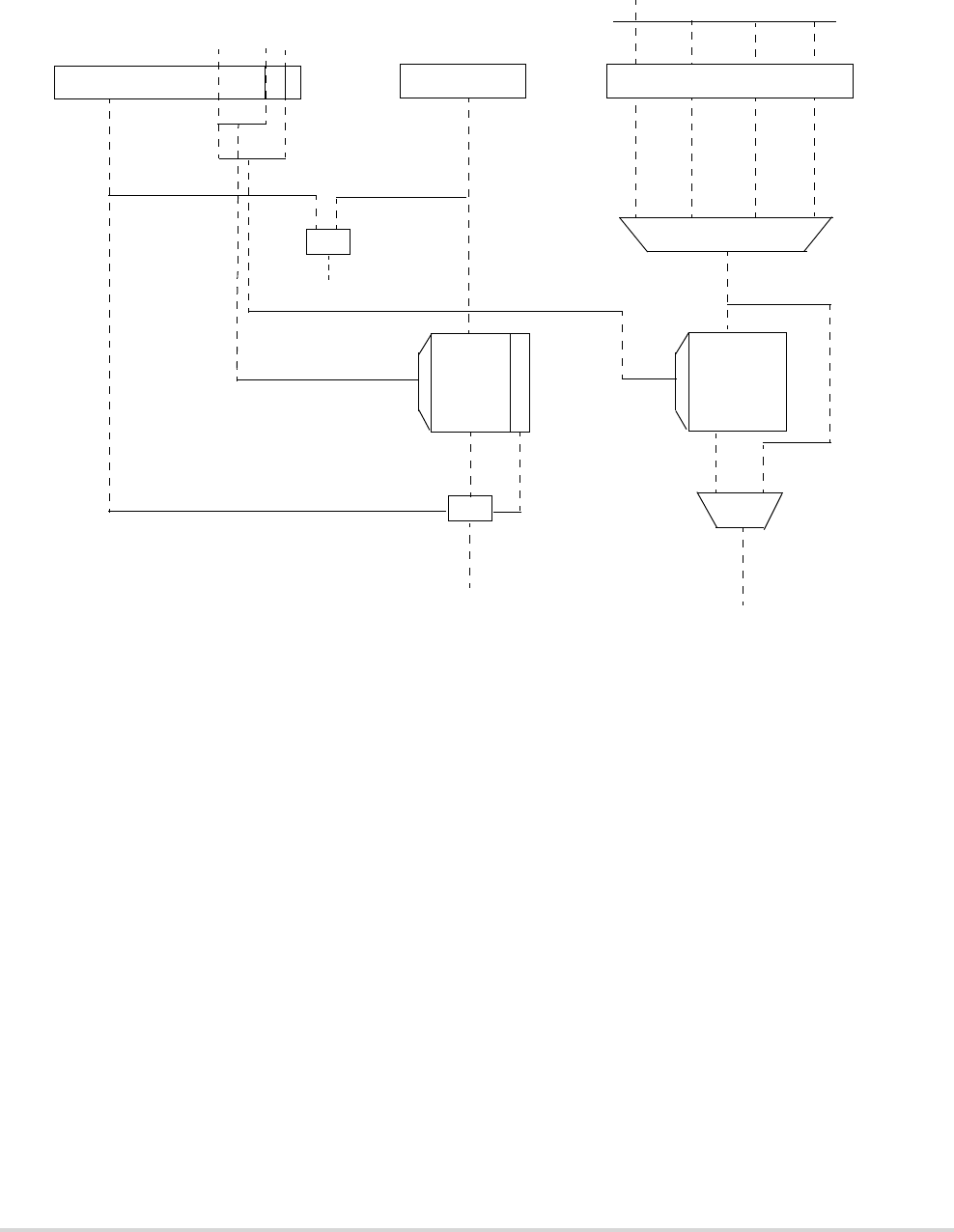
MOTOROLA Chapter 4. Cache 4-3
Cache Operation
Figure 4-1. Cache Block Diagram
4.3 Cache Operation
The cache is physically connected to the ColdFire core's local bus, allowing it to service all
fetches from the ColdFire core and certain memory fetches initiated by the debug module.
Typically, the debug module's memory references appear as supervisor data accesses but
the unit can be programmed to generate user-mode accesses and/or instruction fetches. The
cache processes any fetch access in the normal manner.
4.3.1 Interaction with Other Modules
Because both the cache and high-speed SRAM module are connected to the ColdFire core's
local data bus, certain user-defined configurations can result in simultaneous fetch
processing.
If the referenced address is mapped into the SRAM module, that module will service the
request in a single cycle. In this case, data accessed from the cache is simply discarded and
no external memory references are generated. If the address is not mapped into the SRAM
space, the cache handles the request in the normal fashion.
31 10 430
1
231 4
=
=
31 11 31 0
‘512
128
0
0
Local Address Bus
I or D Line Buffer
Address
External Data[31:0]
I or D Line Buffer Storage
MUX
DATA
MUX
Fill Hit
TAG
VA L I D
Local Data Bus
Tag Hit

4-4 MCF5282 User’s Manual MOTOROLA
Cache Operation
4.3.2 Memory Reference Attributes
For every memory reference the ColdFire core or the debug module generates, a set of
“effective attributes” is determined based on the address and the access control registers
(ACRs). This set of attributes includes the cacheable/noncacheable definition, the
precise/imprecise handling of operand write, and the write-protect capability.
In particular, each address is compared to the values programmed in the ACRs. If the
address matches one of the ACR values, the access attributes from that ACR are applied to
the reference. If the address does not match either ACR, then the default value defined in
the cache control register (CACR) is used. The specific algorithm is as follows:
if (address == ACR0_address including mask)
Effective Attributes = ACR0 attributes
else if (address == ACR1_address including mask)
Effective Attributes = ACR1 attributes
else Effective Attributes = CACR default attributes
4.3.3 Cache Coherency and Invalidation
The cache does not monitor ColdFire core data references for accesses to cached
instructions. Therefore, software must maintain instruction cache coherency by
invalidating the appropriate cache entries after modifying code segments if instructions are
cached.
The cache invalidation can be performed in several ways. For the instruction- or data-only
configurations, setting CACR[CINV] forces the entire cache to be marked as invalid. The
invalidation operation requires 128 cycles because the cache sequences through the entire
tag array, clearing a single location each cycle. For the split configuration, CACR[INVI]
and CACR[INVD] can be used in addition to CACR[CINV] to clear the entire cache, only
the instruction half, or only the data half. Any subsequent fetch accesses are postponed until
the invalidation sequence is complete.
The privileged CPUSHL instruction can invalidate a single cache line. When this
instruction is executed, the cache entry defined by bits [10:4] of the source address register
is invalidated, provided CACR[CPDI] is cleared. For the split data/instruction cache
configuration, software directly controls bit 10 which selects whether an instruction cache
or data cache line is being accessed.
These invalidation operations can be initiated from the ColdFire core or the debug module.

MOTOROLA Chapter 4. Cache 4-5
Cache Operation
4.3.4 Reset
A hardware reset clears the CACR and disables the cache. The contents of the tag array are
not affected by the reset. Accordingly, the system startup code must explicitly perform a
cache invalidation by setting CACR[24] before the cache can be enabled.
4.3.5 Cache Miss Fetch Algorithm/Line Fills
As discussed in Section 4.2, “Cache Physical Organization,” the cache hardware includes
a 16-byte line-fill buffer for providing temporary storage for the last fetched line.
With the cache enabled as defined by CACR[CENB], a cacheable fetch that misses in both
the tag memory and the line-fill buffer generates an external fetch. For data misses, the size
of the external fetch is always 16 bytes. For instruction misses, the size of the external fetch
is determined by the value contained in the 2-bit CLNF field of the CACR and the miss
address. Table 4-1 shows the relationship between the CLNF bits, the miss address, and the
size of the external fetch.
Depending on the runtime characteristics of the application and the memory response
speed, overall performance may be increased by programming the CLNF bits to values {00,
01}.
For all cases of a line-sized fetch, the critical longword defined by bits [3:2] of the miss
address is accessed first followed by the remaining three longwords that are accessed by
incrementing the longword address in a modulo-16 fashion as shown below:
if miss address[3:2] = 00
fetch sequence = {0x0, 0x4, 0x8, 0xC}
if miss address[3:2] = 01
fetch sequence = {0x4, 0x8, 0xC, 0x0}
if miss address[3:2] = 10
fetch sequence = {0x8, 0xC, 0x0, 0x4}
if miss address[3:2] = 11
fetch sequence = {0xC, 0x0, 0x4, 0x8}
Table 4-1. Initial Fetch Offset vs. CLNF Bits
CLNF[1:0]
Longword Address Bits
00 01 10 11
00 Line Line Line Longword
01 Line Line Longword Longword
1X Line Line Line Line

4-6 MCF5282 User’s Manual MOTOROLA
Cache Operation
Once an external fetch has been initiated and the data is loaded into the line-fill buffer, the
cache maintains a special “most-recently-used” indicator that tracks the contents of the
associated line-fill buffer versus its corresponding cache location. At the time of the miss,
the hardware indicator is set, marking the line-fill buffer as “most recently used.” If a
subsequent access occurs to the cache location defined by bits [10:4] (or bits [9:4] for split
configurations of the fill buffer address), the data in the cache memory array is now most
recently used, so the hardware indicator is cleared. In all cases, the indicator defines
whether the contents of the line-fill buffer or the memory data array are most recently used.
At the time of the next cache miss, the contents of the line-fill buffer are written into the
memory array if the entire line is present, and the line-fill buffer data is still most recently
used compared to the memory array.
Generally, longword references are used for sequential instruction fetches. If the processor
branches to an odd word address, a word-sized instruction fetch is generated.
For instruction fetches, the fill buffer can also be used as temporary storage for line-sized
bursts of non-cacheable references under control of CACR[CEIB]. With this bit set, a
noncacheable instruction fetch is processed as defined by Table 4-2. For this condition, the
line-fill buffer is loaded and subsequent references can hit in the buffer, but the data is never
loaded into the memory array.
Table 4-2 shows the relationship between CACR bits 31 and 10 and the type of instruction
fetch.
Table 4-2. Instruction Cache Operation as Defined by CACR[31, 10]
CACR[31] CACR[10] Type of Instruction Fetch Description
0 0 N/A Cache is completely disabled; all instruction fetches are
word or longword in size.
0 1 N/A All instruction fetches are word or longword in size
1 X Cacheable Fetch size is defined by Table 4-1 and contents of the
line-fill buffer can be written into the memory array
1 0 Noncacheable All instruction fetches are word or longword in size, and
not loaded into the line-fill buffer
1 1 Noncacheable Instruction fetch size is defined by Table 4-1 and loaded
into the line-fill buffer, but are never written into the
memory array.

MOTOROLA Chapter 4. Cache 4-7
Cache Programming Model
4.4 Cache Programming Model
Three supervisor registers define the operation of the cache and local bus controller: the
cache control register (CACR) and two access control registers (ACR0, ACR1).
4.4.1 Cache Registers Memory Map
Table 4-3 below shows the memory map of the cache and access control registers.
The following lists several keynotes regarding the programming model table:
• The CACR and ACRs can only be accessed in supervisor mode using the MOVEC
instruction with an Rc value of 0x002, 0x004 and 0x005, respectively.
• Addresses not assigned to the registers and undefined register bits are reserved for
future expansion. Write accesses to these reserved address spaces and reserved
register bits have no effect, and read accesses will return zeros.
• The reset value column indicates the register initial value at reset. Certain registers
may be uninitialized upon reset; that is, they may contain random values after reset.
• The access column indicates if the corresponding register allows both read/write
functionality (R/W), read-only functionality (R), or write-only functionality (W). If
a read access to a write-only register is attempted, zeros will be returned. If a write
access to a read-only register is attempted, the access will be ignored and no write
will occur.
4.4.2 Cache Registers
4.4.2.1 Cache Control Register (CACR)
The CACR controls the operation of the cache. The CACR provides a set of default
memory access attributes used when a reference address does not map into the spaces
defined by the ACRs.
The CACR is a 32-bit write-only supervisor control register. It is accessed in the CPU
address space via the MOVEC instruction with an Rc encoding of 0x002. The CACR can
be read when in background debug mode (BDM). At system reset, the entire register is
cleared.
Table 4-3. Memory Map of Cache Registers
Address Name Width Description Reset Value Access
MOVEC with 0x002 CACR 32 Cache Control Register 0x0000_0000 W
MOVEC with 0x004 ACR0 32 Access Control Register 0 0x0000_0000 W
MOVEC with 0x005 ACR1 32 Access Control Register 1 0x0000_0000 W

4-8 MCF5282 User’s Manual MOTOROLA
Cache Programming Model
31 30 29 28 27 26 25 24 23 22 21 20 19 16
Field CENB — CPD CFRZ — CINV DIDI DISD INVI INVD —
Reset 0000_0000_0000_0000
R/W W
15 11 10 9 8 7 6 5 4 3 2 1 0
Field — CEIB DCM DBWE — DWP EUSP — CLNF
Reset 0000_0000_0000_0000
R/W W
Figure 4-2. Cache Control Register (CACR)
Table 4-4. CACR Field Descriptions
Bits Name Description
31 CENB Cache enable. The memory array of the cache is enabled only if CENB is asserted. This bit, along with
the DISI (disable instruction caching) and DISD (disable data caching) bits, control the cache
configuration.
0 Cache disabled
1 Cache enabled
Table 4-5 describes cache configuration.
30–29 — Reserved, should be cleared.
28 CPDI Disable CPUSHL invalidation. When the privileged CPUSHL instruction is executed, the cache entry
defined by bits [10:4] of the address is invalidated if CPDI = 0. If CPDI = 1, no operation is performed.
0 Enable invalidation
1 Disable invalidation
27 CFRZ Cache freeze. This field allows the user to freeze the contents of the cache. When CFRZ is asserted line
fetches can be initiated and loaded into the line-fill buffer, but a valid cache entry can not be overwritten.
If a given cache location is invalid, the contents of the line-fill buffer can be written into the memory
array while CFRZ is asserted.
0 Normal Operation
1 Freeze valid cache lines
26–25 — Reserved, should be cleared.
24 CINV Cache invalidate. The cache invalidate operation is not a function of the CENB state (that is, this
operation is independent of the cache being enabled or disabled). Setting this bit forces the cache to
invalidate all, half, or none of the tag array entries depending on the state of the DISI, DISD, INVI, and
INVD bits. The invalidation process requires several cycles of overhead plus 128 machine cycles to
clear all tag array entries and 64 cycles to clear half of the tag array entries, with a single cache entry
cleared per machine cycle. The state of this bit is always read as a zero. After a hardware reset, the cache
must be invalidated before it is enabled.
0 No operation
1 Invalidate all cache locations
Table 4-6 describes how to set the cache invalidate all bit.
23 DISI Disable instruction caching. When set, this bit disables instruction caching. This bit, along with the
CENB (cache enable) and DISD (disable data caching) bits, control the cache configuration. See the
CENB definition for a detailed description.
0 Do not disable instruction caching
1 Disable instruction caching
Table 4-5 describes cache configuration and Table 4-6 describes how to set the cache invalidate all bit.

MOTOROLA Chapter 4. Cache 4-9
Cache Programming Model
22 DISD Disable data caching. When set, this bit disables data caching. This bit, along with the CENB (cache
enable) and DISI (disable instruction caching) bits, control the cache configuration. See the CENB
definition for a detailed description.
0 Do not disable data caching
1 Disable data caching
Table 4-5 describes cache configuration and Table 4-6 describes how to set the cache invalidate all bit.
21 INVI CINV instruction cache only. This bit can not be set unless the cache configuration is split (both DISI
and DISD cleared). For instruction or data cache configurations this bit is a don’t-care. For the split
cache configuration, this bit is part of the control for the invalidate all operation. See the CINV
definition for a detailed description
Table 4-6 describes how to set the cache invalidate all bit.
20 INVD CINV data cache only. This bit can not be set unless the cache configuration is split (both DISI and
DISD cleared). For instruction or data cache configurations this bit is a don’t-care. For the split cache
configuration, this bit is part of the control for the invalidate all operation. See the CINV definition for
a detailed description
Table 4-6 describes how to set the cache invalidate all bit.
19–11 — Reserved, should be cleared.
10 CEIB Cache enable noncacheable instruction bursting. Setting this bit enables the line-fill buffer to be loaded
with burst transfers under control of CLNF[1:0] for noncacheable accesses. Noncacheable accesses are
never written into the memory array.
0 Disable burst fetches on noncacheable accesses
1 Enable burst fetches on noncacheable accesses
9 DCM Default cache mode. This bit defines the default cache mode: 0 is cacheable, 1 is noncacheable. For
more information on the selection of the effective memory attributes, see Section 4.3.2, “Memory
Reference Attributes.
0 Caching enabled
1 Caching disabled
8 DBWE Default buffered write enable. This bit defines the default value for enabling buffered writes. If DBWE
= 0, the termination of an operand write cycle on the processor's local bus is delayed until the external
bus cycle is completed. If DBWE = 1, the write cycle on the local bus is terminated immediately and
the operation buffered in the bus controller. In this mode, operand write cycles are effectively decoupled
between the processor's local bus and the external bus. Generally, enabled buffered writes provide
higher system performance but recovery from access errors can be more difficult. For the ColdFire CPU,
reporting access errors on operand writes is always imprecise and enabling buffered writes further
decouples the write instruction and the signaling of the fault
0 Disable buffered writes
1 Enable buffered writes
7–6 — Reserved, should be cleared.
5 DWP Default write protection
0 Read and write accesses permitted
1 Only read accesses permitted
4 EUSP Enable user stack pointer. See Section 2.2.3.2, “Supervisor/User Stack Pointers (A7 and OTHER_A7)"
for more information on the dual stack pointer implementation.
0 Disable the processor’s use of the User Stack Pointer
1 Enable the processor’s use of the User Stack Pointer
Table 4-4. CACR Field Descriptions (continued)
Bits Name Description

4-10 MCF5282 User’s Manual MOTOROLA
Cache Programming Model
Table 4-5 shows the relationship between CACR bits 31, 23, and 22 and the cache
configuration.
Table 4-6 shows the relationship between CACR bits 23, 22, 21 and 20 and setting the
cache invalidate all bit.
3–2 — Reserved, should be cleared.
1–0 CLNF Cache line fill. These bits control the size of the memory request the cache issues to the bus controller
for different initial instruction line access offsets. See Table 4-7 for external fetch size based on miss
address and CLNF.
Table 4-5. Cache Configuration as Defined by CACR[31, 23, 22]
CACR[31] CACR[23] CACR[22] Configuration Description
0 x x N/A Cache is completely disabled
1 0 0 Split Instruction/
Data Cache
1 KByte direct-mapped instruction cache (uses lower half
of tag and storage arrays) and 1 KByte direct-mapped
write-through data cache (uses upper half of tag and storage
arrays)
1 0 1 Instruction Cache 2 KByte direct-mapped instruction cache (uses all of tag
and storage arrays)
1 1 0 Data Cache 2 KByte direct-mapped write-through data cache (uses all
of tag and storage arrays)
Table 4-6. Cache Invalidate All as Defined by CACR[23, 22, 21, 20]
CACR[23] CACR[22] CACR[21] CACR[20] Configuration Operation
0 0 0 0 Split Instruction/
Data Cache
Invalidate all entries in both 1 KByte instruction
cache and 1 KByte data cache
0 0 0 1 Split Instruction/
Data Cache
Invalidate only 1 KByte data cache
0 0 1 0 Split Instruction
Data Cache
Invalidate only 1 KByte instruction cache
0 0 1 1 Split Instruction/
Data Cache
No invalidate
1 0 x x Instruction Cache Invalidate 2 KByte instruction cache
0 1 x x Data Cache Invalidate 2 KByte data cache
Table 4-4. CACR Field Descriptions (continued)
Bits Name Description

MOTOROLA Chapter 4. Cache 4-11
Cache Programming Model
4.4.2.2 Access Control Registers (ACR0, ACR1)
The ACRs provide a definition of memory reference attributes for two memory regions
(one per ACR). This set of effective attributes is defined for every memory reference using
the ACRs or the set of default attributes contained in the CACR. The ACRs are examined
for every processor memory reference that is not mapped to the Flash or SRAM memories.
The ACRs are 32-bit write-only supervisor control register. They are accessed in the CPU
address space via the MOVEC instruction with an Rc encoding of 0x004 and 0x005. The
ACRs can be read when in background debug mode (BDM). At system reset, both registers
are cleared.
Table 4-7. External Fetch Size Based on Miss Address and CLNF
CLNF[1:0]
Longword Address Bits
00 01 10 11
00 Line Line Line Longword
01 Line Line Longword Longword
10 Line Line Line Line
11 Line Line Line Line
31 24 23 16
Field AB AM
Reset 0000_0000_0000_0000
R/W W
15 14 13 12 7 6 5 4321 0
Field EN SM — CM BUFW — WP —
Reset 0000_0000_0000_0000
R/W W
Figure 4-3. Access Control Registers (ACR0, ACR1)
Table 4-8. ACR Field Descriptions
Bits Name Description
31–24 AB Address base. This 8-bit field is compared to address bits [31:24] from the processor's local bus under
control of the ACR address mask. If the address matches, the attributes for the memory reference are
sourced from the given ACR.
22–16 AM Address mask. This 8-bit field can mask any bit of the AB field comparison. If a bit in the AM field is
set, then the corresponding bit of the address field comparison is ignored.
15 EN Enable. The EN bit defines the ACR enable. Hardware reset clears this bit, disabling the ACR.
0 ACR disabled
1 ACR enabled

4-12 MCF5282 User’s Manual MOTOROLA
Cache Programming Model
14–13 SM Supervisor mode. This two-bit field allows the given ACR to be applied to references based on
operating privilege mode of the ColdFire processor. The field uses the ACR for user references only,
supervisor references only, or all accesses.
00 Match if user mode
01 Match if supervisor mode
1x Match always—ignore user/supervisor mode
12–7 — Reserved, should be cleared.
6 CM Cache mode. This bit defines the cache mode: 0 is cacheable, 1 is noncacheable.
0 Caching enabled
1 Caching disabled
5 BWE Buffered write enable. This bit defines the value for enabling buffered writes. If BWE = 0, the
termination of an operand write cycle on the processor's local bus is delayed until the external bus cycle
is completed. If BWE = 1, the write cycle on the local bus is terminated immediately and the operation
is then buffered in the bus controller. In this mode, operand write cycles are effectively decoupled
between the processor's local bus and the external bus.
Generally, the enabling of buffered writes provides higher system performance but recovery from access
errors may be more difficult. For the V2 ColdFire CPU, the reporting of access errors on operand writes
is always imprecise, and enabling buffered writes simply decouples the write instruction from the
signaling of the fault even more.
0 Writes are not buffered.
1 Writes are buffered.
4–3 — Reserved, should be cleared.
2 WP Write protect. The WP bit defines the write-protection attribute. If the effective memory attributes for a
given access select the WP bit, an access error terminates any attempted write with this bit set.
0 Read and write accesses permitted
1 Only read accesses permitted
1–0 — Reserved, should be cleared.
Table 4-8. ACR Field Descriptions (continued)
Bits Name Description

MOTOROLA Chapter 5. Static RAM (SRAM) 5-1
Chapter 5
Static RAM (SRAM)
5.1 SRAM Features
• One 64-Kbyte SRAM
• Single-cycle access
• Physically located on processor's high-speed local bus
• Memory location programmable on any 0-modulo-64 Kbyte address
• Byte, word, longword address capabilities
5.2 SRAM Operation
The SRAM module provides a general-purpose memory block that the ColdFire processor
can access in a single cycle. The location of the memory block can be specified to any
0-modulo-64K address within the 4-GByte address space. The memory is ideal for storing
critical code or data structures or for use as the system stack. Because the SRAM module
is physically connected to the processor's high-speed local bus, it can service
processor-initiated access or memory-referencing commands from the debug module.
Depending on configuration information, instruction fetches may be sent to both the cache
and the SRAM block simultaneously. If the reference is mapped into the region defined by
the SRAM, the SRAM provides the data back to the processor, and the cache data
discarded. Accesses from the SRAM module are not cached.
The SRAM is dual-ported to provide DMA access. The SRAM is partitioned into two
physical memory arrays to allow simultaneous access to both arrays by the processor core
and another bus master. See Chapter 5, “System Control Module (SCM)” for more
information.
5.3 SRAM Programming Model
The SRAM programming model includes a description of the SRAM base address register
(RAMBAR), SRAM initialization, and power management.

5-2 MCF5282 User’s Manual MOTOROLA
SRAM Programming Model
5.3.1 SRAM Base Address Register (RAMBAR)
The configuration information in the SRAM base address register (RAMBAR) controls the
operation of the SRAM module.
• The RAMBAR holds the base address of the SRAM. The MOVEC instruction
provides write-only access to this register.
• The RAMBAR can be read or written from the debug module in a similar manner.
• All undefined bits in the register are reserved. These bits are ignored during writes
to the RAMBAR, and return zeroes when read from the debug module.
• The RAMBAR valid bit is cleared by reset, disabling the SRAM module. All other
bits are unaffected.
The RAMBAR contains several control fields. These fields are shown in Figure 5-1
31 30 29 28 27 26 25 24 23 22 21 20 19 18 17 16
Field BA31 BA30 BA29 BA28 BA27 BA26 BA25 BA24 BA23 BA22 BA21 BA20 BA19 BA18 BA17 BA16
Reset Undefined
R/W W
1514131211109876543210
Field — PRI1 PRI2 SPV WP — C/I SC SD UC UD V
Reset Undefined 0
R/W W
Address CPU + 0xC05
Figure 5-1. SRAM Base Address Register (RAMBAR)
Table 5-1. SRAM Base Address Register
Bits Name Description
31–16 BA Base address. Defines the 0-modulo-64K base address of the SRAM module. By
programming this field, the SRAM may be located on any 64-Kbyte boundary within the
processor’s 4-Gbyte address space.
15–12 — Reserved, should be cleared.
11–10 PRI1, PRI2 Priority bit. PRI1 determines if DMA or CPU has priority in upper 32k bank of memory. PRI2
determines if DMA or CPU has priority in lower 32k bank of memory. If bit is set, DMA has
priority. If bit is reset, CPU has priority. Priority is determined according to the following
table.
NOTE: The Motorola-recommended setting for the priority bits is 00.
PRI[1:2] Upper Bank
Priority
Lower Bank
Priority
00 DMA Accesses DMA Accesses
01 DMA Accesses CPU Accesses
10 CPU Accesses DMA Accesses
11 CPU Accesses CPU Accesses

MOTOROLA Chapter 5. Static RAM (SRAM) 5-3
SRAM Programming Model
5.3.2 SRAM Initialization
After a hardware reset, the contents of the SRAM module are undefined. The valid bit of
the RAMBAR is cleared, disabling the module. If the SRAM requires initialization with
instructions or data, the following steps should be performed:
1. Load the RAMBAR mapping the SRAM module to the desired location within the
address space.
2. Read the source data and write it to the SRAM. There are various instructions to
support this function, including memory-to-memory move instructions, or the
MOVEM opcode. The MOVEM instruction is optimized to generate line-sized
burst fetches on 0-modulo-16 addresses, so this opcode generally provides
maximum performance.
3. After the data has been loaded into the SRAM, it may be appropriate to load a
revised value into the RAMBAR with a new set of attributes. These attributes
consist of the write-protect and address space mask fields.
9 SPV Secondary port valid. Allows access by DMA
0 DMA access to memory is disabled.
1 DMA access to memory is enabled.
NOTE: The BDE bit in the second RAMBAR register must also be set to allow dual port
access to the SRAM. For more information, see Section 8.4.2, “Memory Base Address
Register (RAMBAR).”
8 WP Write protect. Allows only read accesses to the SRAM. When this bit is set, any attempted
write access will generate an access error exception to the ColdFire processor core.
0 Allows read and write accesses to the SRAM module
1 Allows only read accesses to the SRAM module
7–6 — Reserved, should be cleared.
5–1 C/I, SC, SD,
UC, UD
Address space masks (ASn)
These five bit fields allow certain types of accesses to be “masked,” or inhibited from
accessing the SRAM module. The address space mask bits are:
C/I = CPU space/interrupt acknowledge cycle mask
SC = Supervisor code address space mask
SD = Supervisor data address space mask
UC = User code address space mask
UD = User data address space mask
For each address space bit:
0 An access to the SRAM module can occur for this address space
1 Disable this address space from the SRAM module. If a reference using this address
space is made, it is inhibited from accessing the SRAM module, and is processed like
any other non-SRAM reference.
These bits are useful for power management as detailed in Section 5.3.4, “Power
Management.”
0 V Valid. A hardware reset clears this bit. When set, this bit enables the SRAM module;
otherwise, the module is disabled.
0 Contents of RAMBAR are not valid
1 Contents of RAMBAR are valid
Table 5-1. SRAM Base Address Register (continued)
Bits Name Description

5-4 MCF5282 User’s Manual MOTOROLA
SRAM Programming Model
The ColdFire processor or an external emulator using the debug module can perform these
initialization functions.
5.3.3 SRAM Initialization Code
The following code segment describes how to initialize the SRAM. The code sets the base
address of the SRAM at 0x20000000 and then initializes the SRAM to zeros.
RAMBASE EQU $20000000 ;set this variable to $20000000
RAMVALID EQU $00000001
move.l #RAMBASE+RAMVALID,D0 ;load RAMBASE + valid bit into D0.
movec.l D0, RAMBAR ;load RAMBAR and enable SRAM
The following loop initializes the entire SRAM to zero
lea.l RAMBASE,A0 ;load pointer to SRAM
move.l #16384,D0 ;load loop counter into D0
SRAM_INIT_LOOP:
clr.l (A0)+) ;clear 4 bytes of SRAM
subq.l #1,D0 ;decrement loop counter
bne.b SRAM_INIT_LOOP ;if done, then exit; else continue
looping
5.3.4 Power Management
As noted previously, depending on the configuration defined by the RAMBAR, instruction
fetch and operand read accesses may be sent to the SRAM and cache simultaneously. If the
access is mapped to the SRAM module, it sources the read data and the unified cache access
is discarded. If the SRAM is used only for data operands, asserting the ASn bits associated
with instruction fetches can decrease power dissipation. Additionally, if the SRAM
contains only instructions, masking operand accesses can reduce power dissipation.
Table 5-2 shows some examples of typical RAMBAR settings.
Table 5-2. Typical RAMBAR Setting Examples
Data Contained in SRAM RAMBAR[7:0]
Code Only 0x2B
Data Only 0x35
Both Code And Data 0x21

MOTOROLA Chapter 5. Static RAM (SRAM) 5-5
SRAM Programming Model

5-6 MCF5282 User’s Manual MOTOROLA
SRAM Programming Model

MOTOROLA Chapter 6. ColdFire Flash Module (CFM) 6-1
Chapter 6
ColdFire Flash Module (CFM)
The MCF5282 incorporates SuperFlash® technology licensed from SST. The ColdFire
Flash Module (CFM) is constructed with eight banks of 32K x 16-bit Flash to generate a
512-Kbyte, 32-bit wide electrically erasable and programmable read-only memory array.
The CFM is ideal for program and data storage for single-chip applications and allows for
field reprogramming without external high-voltage sources.
The voltage required to program and erase the Flash is generated internally by on-chip
charge pumps. Program and erase operations are performed under CPU control through a
command-driven interface to an internal state machine. All Flash physical blocks can be
programmed or erased at the same time; however, it is not possible to read from a Flash
physical block while the same block is being programmed or erased. The array used in the
MCF5282 makes it possible to program or erase one pair of Flash physical blocks under the
control of software routines executing out of another pair.
NOTE
The MCF5281 implements only 256 Kbytes of Flash; half that
of the MCF5282.
6.1 Features
Features of the CFM include:
• 512-Kbytes of Flash memory on the MCF5282 and 256-Kbytes of Flash memory on
the MCF5281
• Basic Flash access time of 2 clock cycles. Optimized processor Flash interface
reduces basic Flash access time through interleaving and speculative reads.
• Automated program and erase operation
• Concurrent verify, program, and erase of all array blocks
• Read-while-write capability
• Optional interrupt on command completion
• Flexible scheme for protection against accidental program or erase operations
• Access restriction controls for both supervisor/user and data/program space
operations

6-2 MCF5282 User’s Manual MOTOROLA
Block Diagram
• Security for single-chip applications
• Single power supply (system VDD) used for all module operations
• Auto-sense amplifier timeout for low-power, low-frequency read operations
NOTE
Enabling Flash security will disable BDM communications.
NOTE
When Flash security is enabled, the chip will boot in
single-chip mode regardless of the external reset configuration.
6.2 Block Diagram
The CFM module shown in Figure 6-1 contains the Flash physical blocks, the ColdFire
Flash bus and IP bus interfaces, Flash interface, register blocks, and the BIST engine.
Each 128-Kbyte Flash physical block is arranged as two 32,768-word (16 bits) memory
arrays. Each of these memory arrays is designated as xH or xL, where x represents one of
the four Flash physical blocks (0–3) and H/L represents the high or low 16 bits of each
longword of logical memory. Each of these words may be read as either individual bytes or
aligned words. Aligned longword access is provided by concatenating the outputs of the
each of the two memory arrays within the Flash physical block. Simple reads of bytes,
aligned words, and aligned longwords require two 66-MHz clock cycles, although the
processor’s Flash interface includes logic that reduces the effective access time through
two-way longword interleaving and speculative reads.
Flash physical blocks are interleaved on longword (4-byte) boundaries. Therefore, all Flash
program, erase, and verify commands operate on adjacent Flash physical blocks and are
initiated with a single aligned 32-bit write to the appropriate array location. Any other write
operation will cause a cycle termination transfer error. Page erase operates simultaneously
on two interleaving erase pages in adjacent Flash physical blocks. Each Flash physical
block is organized as 1024 rows of 128 bytes with a single erase page consisting of 8 rows
(1024 bytes). Since page erase operates simultaneously on two interleaving and adjacent
physical Flash blocks, each erase row is comprised of four 16-bit entries in each of two
memory arrays within each of two Flash physical blocks. The first row of Flash is made up
of 0H_0L_1H_1L [0] through 0H_0L_1H_1L [31], where each [n] represents four 16-bit
words from each memory array in each of two physical blocks, for a total of 256 bytes.
Since a single erase page consists of 8 rows of 256 bytes, or 2048 bytes, the first erase page
is physically located at 0H_0L_1H_1L [0] through 0H_0L_1H_1L [255]. Mass erase
operates simultaneously on two adjacent Flash physical blocks in their entirety and erases
a total of 256 Kbytes of Flash space. Therefore, it takes two mass erase operations, one on
mass erase block 0 and one on mass erase block 1, to erase the full 512K CFM Flash on the
MCF5282.
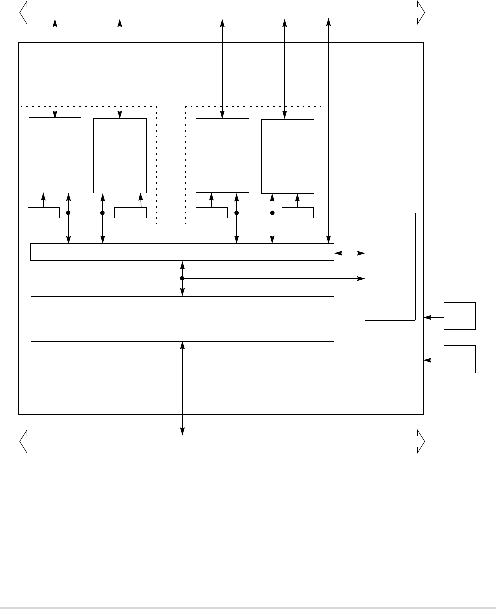
MOTOROLA Chapter 6. ColdFire Flash Module (CFM) 6-3
Block Diagram
An erased Flash bit reads 1 and a programmed Flash bit reads 0. The CFM features a sense
amplifier timeout (SATO) block that automatically reduces current consumption during
reads at low system clock frequencies.
Figure 6-1. CFM Block Diagram
Flash Interface
•
•
•
SATOSATOSATOSATO
BIST
Engine
Internal Bus
Memory Array
Backdoor Access
Flash Control Registers
Block 0H
32K x 16
Memory Array
Block 0L
32K x 16
Memory Array
Block 3H
32K x 16
Memory Array
Block 3L
32K x 16
Flash Physical
Block 0
Flash Physical
Block 3
Note:
Mass Erase Block 0 (256 Kbytes) = Flash Physical Block 0 and Flash Physical Block 1.
Mass Erase Block 1 (256 Kbytes) = Flash Physical Block 2 and Flash Physical Block 3 (MCF5282 only)
VDDF
VSSF
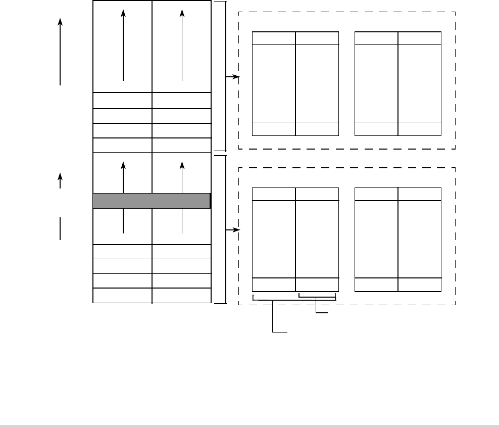
6-4 MCF5282 User’s Manual MOTOROLA
Memory Map
6.3 Memory Map
Figure 6-2 shows the memory map for the CFM array. The CFM array can reside anywhere
in the memory space of the MCU. The starting address of the array is determined by the
CFM array base address which must reside on a natural size boundary; that is, the CFM
array base address must be an integer multiple of the array size. The CFM register space
must reside on a 64 byte boundary as determined by the CFM register base address.
Figure 6-2 shows how multiple 32,768 by 16-bit Flash physical blocks interleave to form a
contiguous non-volatile memory space. Each pair of 32-bit blocks (even and odd)
interleave every 4 bytes to form a 256-Kbyte section of memory.
NOTE
The CFM on the MCF5281 is constructed with four banks of
32K x 16-bit Flash arrays to generate 256 Kbytes of 32-bit
Flash memory.
Figure 6-2. CFM Array Memory Map
0x0007 FFFF
0x0004 000C
0x0000 0000
0x0000 0004
0x0000 0008
0x0000 000C
0x0003 FFFF
0x0004 0000
0x0004 0004
0x0004 0008
3H[1] 3L[1]
2H[1] 2L[1]
3H[0] 3L[0]
2H[0] 2L[0]
1H[1] 1L[1]
0H[1] 0L[1]
1H[1] 1L[1]
0H[0] 0L[0]
Logical Block 1 (256 Kbytes)
Memory
Array 2H
2H[31] 2L[31]
Memory
Array 2L
2H[0] 2L[0]
Flash Physical Block 2 Flash Physical Block 3
3H[31] 3L[31]
3H[0] 3L[0]
Memory
Array 3H
Memory
Array 3L
Logical Block 0 (256 Kbytes)
Memory
Array 0H
0H[31] 0L[31]
Memory
Array 0L
0H[0] 0L[0]
Flash Physical Block 0 Flash Physical Block 1
1H[31] 1L[31]
1H[0] 1L[0]
Memory
Array 1H
Memory
Array 1L
Each memory array = 64 Kbytes
(16 bits wide × 32K)
Each physical block = 128 Kbytes
(32 bits wide × 32K)
Configuration Field
(0x0000_0400–
0x0000_0417)
1The MCF5281 supports only Logical Block 0.

MOTOROLA Chapter 6. ColdFire Flash Module (CFM) 6-5
Memory Map
The CFM module has hardware interlocks to protect data from accidental corruption. The
CFM memory array is logically divided into 16-Kbyte sectors for the purpose of data
protection and access control. A flexible scheme allows the protection of any combination
of logical sectors (see Section 6.3.4.4, “CFM Protection Register (CFMPROT)”). A similar
mechanism is available to control supervisor/user and program/data space access to these
sectors.
6.3.1 CFM Configuration Field
The CFM configuration field comprises 24 bytes of reserved array memory space that
determines the module protection and access restrictions out of reset. Data to secure the
Flash from unauthorized access is also stored in the CFM configuration field. Table 6-1
describes each byte used in this field.
6.3.2 Flash Base Address Register (FLASHBAR)
The configuration information in the Flash base address register (FLASHBAR) controls the
operation of the Flash module.
• The FLASHBAR holds the base address of the Flash. The MOVEC instruction
provides write-only access to this register.
• The FLASHBAR can be read or written from the debug module in a similar manner.
• All undefined bits in the register are reserved. These bits are ignored during writes
to the FLASHBAR, and return zeroes when read from the debug module.
• The back door enable bit, FLASHBAR[BDE], is cleared at reset, disabling back
door access to the Flash.
Table 6-1. CFM Configuration Field
Address Offset (from array base
address)
Size
in Bytes Description
0x0000_0400–0x0000_0407 8 Back door comparison key
0x0000_0408–0x0000_040B 4 Flash program/erase sector protection
Blocks 0H/0L (see Section 6.3.4.4, “CFM Protection Register (CFMPROT)”)
0x0000_040C–0x0000_040F 4 Flash supervisor/user space restrictions
Blocks 0H/0L (see Section 6.3.4.5, “CFM Supervisor Access Register
(CFMSACC)”)
0x0000_0410–0x0000_0413 4 Flash program/data space restrictions
Blocks 0H/0L (see Section 6.3.4.6, “CFM Data Access Register
(CFMDACC)”)
0x0000_0414–0x0000_0417 4 Flash security longword (see Section 6.3.4.3, “CFM Security Register
(CFMSEC)”)

6-6 MCF5282 User’s Manual MOTOROLA
Memory Map
• The FLASHBAR valid bit is programmed according to the chip mode selected at
reset (see Chapter 30, “Chip Configuration Module (CCM)” for more details). All
other bits are unaffected.
The FLASHBAR register contains several control fields. These fields are shown in
Figure 6-3
NOTE
The default value of the FLASHBAR is determined by the chip
configuration selected at reset (see Chapter 30, “Chip
Configuration Module (CCM)” for more information). If
external boot mode is used, then the FLASHBAR located in the
processor’s CPU space will be invalid and it must be initialized
with the valid bit set before the CPU (or modules) can access
the on-chip Flash.
NOTE
Flash accesses (reads/writes) by a bus master other than the
core, (DMA controller or Fast Ethernet Controller), or writes to
Flash by the core during programming must use the backdoor
Flash address of IPSBAR plus an offset of 0x0400_0000. For
example, for a DMA transfer from the first location of Flash
when IPSBAR is still at its default location of 0x4000_0000,
the source register would be loaded with 0x4400_0000.
Backdoor access to Flash for reads can be made by the bus
master, but it takes 2 cycles longer than a direct read of the
Flash if using its FLASHBAR address.
NOTE
The Flash is marked as valid on reset based on the RCON (reset
configuration) pin state. Flash space is valid on reset when
booting in single chip mode (RCON pin asserted and
D[26]/D[17]/D[16] set to 110), or when booting internally in
master mode (RCON asserted and D[26]/D[17]/D[16] are set
to 111 and D[18] and D[19] are set to 00). See Chapter 30,
“Chip Configuration Module (CCM)” for more details. When
the default reset configuration is not overriden, the MCF5282
will (by default) boot up in single chip mode and the Flash
space will be marked as valid at address 0x0. The Flash
configuration field is checked during the reset sequence to see
if the Flash is secured. If it is the part will always boot from
internal Flash, since it will be marked as valid, regardless of
what is done for chip configuration.

MOTOROLA Chapter 6. ColdFire Flash Module (CFM) 6-7
Memory Map
31 30 29 28 27 26 25 24 23 22 21 20 19 18 16
Field BA31 BA30 BA29 BA28 BA27 BA26 BA25 BA24 BA23 BA22 BA21 BA20 BA19 —
Reset 0000_0000_0000_0000
R/W R/W
15 9876543210
Field — WP — C/I SC SD UC UD V
Reset 0000_0001_0010_000 See
Note
R/W R/W R R/W R R/W
Address CPU + 0xC04
Note: The reset value for the valid bit is determined by the chip mode selected at reset (see Chapter 30, “Chip
Configuration Module (CCM)”).
Figure 6-3. Flash Base Address Register (FLASHBAR)
Table 6-2. FLASHBAR Field Descriptions
Bits Name Description
31–19 BA[31:18] Base address field. Defines the 0-modulo-512K base address of the Flash module. By
programming this field, the Flash may be located on any 512Kbyte boundary within the
processor’s four gigabyte address space.
18–9 — Reserved, should be cleared.
8 WP Write protect. Allows only read accesses to the Flash. When this bit is set, any attempted
write access will generate an access error exception to the ColdFire processor core.
0 Allows read and write accesses to the Flash module
1 Allows only read accesses to the Flash module
7–6 — Reserved, should be cleared.
5–1 C/I, SC, SD, UC,
UD
Address space masks (ASn).
These five bit fields allow certain types of accesses to be “masked,” or inhibited from
accessing the Flash module. The address space mask bits are:
C/I CPU space/interrupt acknowledge cycle mask
SC Supervisor code address space mask
SD Supervisor data address space mask
UC User code address space mask
UD User data address space mask
For each address space bit:
0 An access to the Flash module can occur for this address space
1 Disable this address space from the Flash module. If a reference using this address
space is made, it is inhibited from accessing the Flash module, and is processed like any
other non-Flash reference.
These bits are useful for power management as detailed in Section 5.3.4, “Power
Management.””
0 V Valid. When set, this bit enables the Flash module; otherwise, the module is disabled.
0 Contents of FLASHBAR are not valid
1 Contents of FLASHBAR are valid
6-8 MCF5282 User’s Manual MOTOROLA
Memory Map
6.3.3 CFM Registers
The CFM module also contains a set of control and status registers. The memory map for
these registers and their accessibility in supervisor and user modes is shown in Table 6-3.
6.3.4 Register Descriptions
The Flash registers are described in this subsection.
6.3.4.1 CFM Configuration Register (CFMCR)
The CFMCR is used to configure and control the operation of the CFM array.
Bits 10 -5 in the CFMCR register are readable and writable with restrictions.
Table 6-3. CFM Register Address Map
IPSBAR Offset Bits 31–24 Bits 23–16 Bits 15–8 Bits 7–0 Access 1
1S = Supervisor access only. User mode accesses to supervisor only addresses have no effect and result in a cycle
termination transfer error.
0x1D_0000 CFMMCR CFMCLKD Reserved 2
2Addresses not assigned to a register and undefined register bits are reserved for expansion. Write accesses to these reserved
address spaces and reserved register bits have no effect.
S
0x1D_0004 Reserved2S
0x1D_0008 CFMSEC S
0x1D_000C Reserved2S
0x1D_0010 CFMPROT S
0x1D_0014 CFMSACC S
0x1D_0018 CFMDACC S
0x1D_001C Reserved2S
0x1D_0020 CFMUSTAT Reserved2S
0x1D_0024 CFMCMD Reserved2S
15 11 10 9 8 7 6 5 4 0
Field — LOCK PVIE AEIE CBEIE CCIE KEYACC —
Reset 0000_0000_0000_0000
R/W R/W
Address IPSBAR + 0x1D_0000
Figure 6-4. CFM Module Configuration Register (CFMCR)

MOTOROLA Chapter 6. ColdFire Flash Module (CFM) 6-9
Memory Map
6.3.4.2 CFM Clock Divider Register (CFMCLKD)
The CFMCLKD is used to set the frequency of the clock used for timed events in program
and erase algorithms.
All bits in CFMCLKD are readable. Bit 7 is a read-only status bit, while bits 6–0 can only
be written once.
Table 6-4. CFMCR Field Descriptions
Bits Name Description
15–11 — Reserved, should be cleared.
10 LOCK Write lock control. The LOCK bit is always readable and is set once.
1 CFMPROT, CMFSACC, and CFMDACC register are write-locked.
0 CFMPROT, CMFSACC, and CFMDACC register are writable.
9 PVIE Protection violation interrupt enable. The PVIE bit is readable and writable. The PVIE bit
enables an interrupt in case the protection violation flag, PVIOL, is set.
1 An interrupt will be requested whenever the PVIOL flag is set.
0 PVIOL interrupts disabled.
8 AEIE Access error interrupt enable. The AEIE bit is readable and writable. The AEIE bit enables
an interrupt in case the access error flag, ACCERR, is set.
1 An interrupt will be requested whenever the ACCERR flag is set.
0 ACCERR interrupts disabled.
7 CBEIE Command buffer empty interrupt enable. The CBEIE bit is readable and writable. CBEIE
enables an interrupt request when the command buffer for the Flash physical blocks is
empty.
1 Request an interrupt whenever the CBEIF flag is set.
0 Command buffer empty interrupts disabled
6 CCIE Command complete interrupt enable. The CCIE bit is readable and writable. CCIE enables
an interrupt when the command executing for the Flash is complete.
1 Request an interrupt whenever the CCIF flag is set.
0 Command complete interrupts disabled
5 KEYACC Enable security key writing. The KEYACC bit is readable and only writable if the KEYEN
bit in the CFMSEC register is set.
1 Writes to the Flash array are interpreted as keys to open the back door.
0 Writes to the Flash array are interpreted as the start of a program, erase, or verify
sequence.
4–0 — Reserved, should be cleared.
765 0
Field DIVLD PRDIV8 DIV
Reset 0000_0000
R/W R R/W
Address IPSBAR + 0x1D_0002
Figure 6-5. CFM Clock Divider Register (CFMCLKD)

6-10 MCF5282 User’s Manual MOTOROLA
Memory Map
NOTE
CFMCLKD must be written with an appropriate value before
programming or erasing the Flash array. Refer to
Section 6.4.3.1, “Setting the CFMCLKD Register.”
6.3.4.3 CFM Security Register (CFMSEC)
The CFMSEC controls the Flash security features.
NOTE
Enabling Flash security will disable BDM communications.
NOTE
When Flash security is enabled, the chip will boot in
single-chip mode regardless of the external reset configuration.
Table 6-5. CFMCLKD Field Descriptions
Bits Name Description
7 DIVLD Clock divider loaded
1 CFMCLKD has been written since the last reset.
0 CFMCLKD has not been written.
6 PRDIV8 Enable prescaler divide by 8
1 Enables a prescaler that divides the CFM clock by 8 before it enters the CFMCLKD
divider.
0 The CFM clock is fed directly into the CFMCLKD divider.
5–0 DIV Clock divider field. The combination of PRDIV8 and DIV[5:0] effectively divides the CFM
input clock down to a frequency between 150 kHz and 200 kHz. The frequency range of the
CFM clock is 150 kHz to 102.4 MHz.
31 30 29 16
Field KEYEN SECSTAT —
Reset See Note
R/W R
15 0
Field SEC
Reset See Note
R/W R
Address IPSBAR + 0x1D_0008
Note: The SECSTAT bit reset value is determined by the security state of the Flash. All other bits in the register are loaded
at reset from the Flash Security longword stored at the array base address + 0x0000_0414.
Figure 6-6. CFM Security Register (CFMSEC)

MOTOROLA Chapter 6. ColdFire Flash Module (CFM) 6-11
Memory Map
The security features of the CFM are described in Section 6.5, “Flash Security Operation.”
Table 6-6. CFMSEC Field Descriptions
Bits Name Description
31 KEYEN Enable back door key to security
1 Back door to Flash is enabled.
0 Back door to Flash is disabled.
30 SECSTAT Flash security status
1 Flash security is enabled
0 Flash security is disabled
29–16 — Reserved. Should be cleared.
15–0 SEC[15:0] Security field. The SEC bits define the security state of the device; see below.
SEC[15:0] Description
0x4AC8 Flash secured 1
1The 0x4AC8 value was chosen because it represents the ColdFire Halt instruction,
making it unlikely that compiled code accidentally programmed at the security
longword in the Flash configuration field location would unintentionally secure the
device.
All other combinations Flash unsecured

6-12 MCF5282 User’s Manual MOTOROLA
Memory Map
6.3.4.4 CFM Protection Register (CFMPROT)
The CFMPROT specifies which Flash logical sectors are protected from program and erase
operations.
The CFMPROT register is always readable and only writeable when LOCK = 0. To change
which logical sectors are protected on a temporary basis, write CFMPROT with a new
value after the LOCK bit in CFMCR has been cleared. To change the value of CFMPROT
that will be loaded on reset, the protection byte in the Flash configuration field must first
be temporarily unprotected using the method just described before reprogramming the
protection bytes. Then the Flash Protection longword at offset 0x1D_0400 must be written
with the desired value.
The CFMPROT controls the protection of thirty-two 16-Kbyte Flash logical sectors in the
512-Kbyte Flash array. Figure 6-8 shows the association between each bit in the
CFMPROT and its corresponding logical sector.
31 16
Field PROT
Reset See Note
R/W R/W
15 0
Field PROT
Reset See Note
R/W R/W
Address IPSBAR + 0x1D_0010
Note: The CFMPROT register is loaded at reset from the Flash Program/Erase Sector Protection longword stored at the
array base address + 0x0000_0400.
Figure 6-7. CFM Protection Register (CFMPROT)
Table 6-7. CFMPROT Field Descriptions
Bits Name Description
31–0 PROT[31:0] Sector protection. Each Flash logical sector can be protected from program and erase
operations by setting its corresponding PROT bit.
1 Logical sector is protected.
0 Logical sector is not protected.
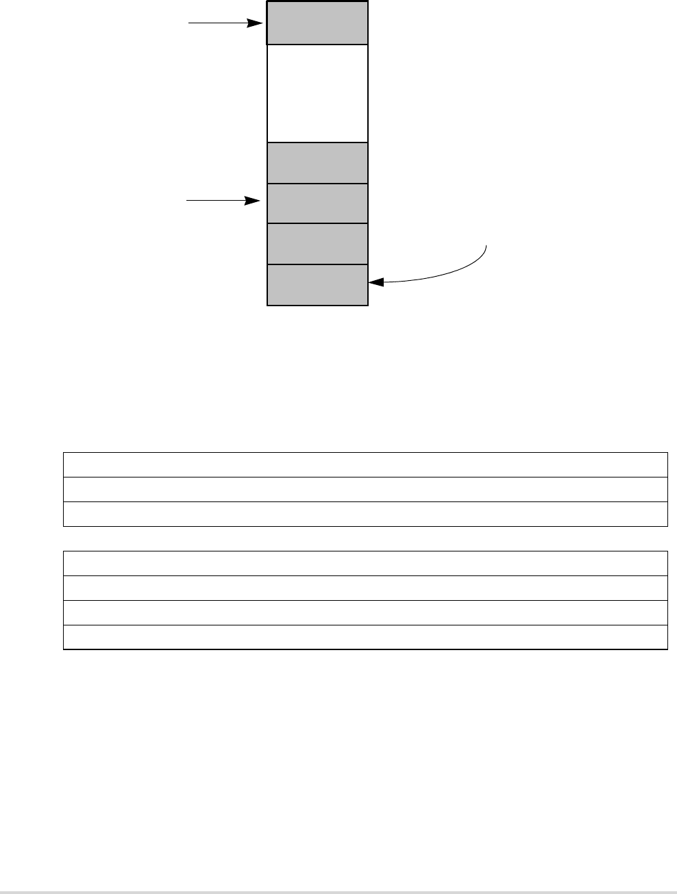
MOTOROLA Chapter 6. ColdFire Flash Module (CFM) 6-13
Memory Map
Figure 6-8. CFMPROT Protection Diagram
6.3.4.5 CFM Supervisor Access Register (CFMSACC)
The CFMSACC specifies the supervisor/user access permissions of Flash logical sectors.
31 16
Field SUPV
Reset See Note
R/W R/W
15 0
Field SUPV
Reset See Note
R/W R/W
Address IPSBAR + 0x1D_0014
Note: The CFMPROT register is loaded at reset from the Flash Supervisor/user Space Restrictions longword stored at the
array base address + 0x0000_040C.
Figure 6-9. CFM Supervisor Access Register (CFMSACC)
(ARRAY_BASE + 0x0000_0000)
}
16Kbyte Sector
(ARRAY_BASE + 0x0007_FFFF)
•
•
•
SECTOR 0
SECTOR 1
SECTOR 2
SECTOR 31
(ARRAY_BASE + 0x0000_4000)
(ARRAY_BASE + 0x0000_8000)
PROTECT[31]
PROTECT[2]
Protected Flash Logical Sectors
as defined by CFMPROT register
(ARRAY_BASE + 0x0007_C000)

6-14 MCF5282 User’s Manual MOTOROLA
Memory Map
6.3.4.6 CFM Data Access Register (CFMDACC)
The CFMDACC specifies the data/program access permissions of Flash logical sectors.
Table 6-8. CFMSACC Field Descriptions
Bits Name Description
31–0 SUPV[31:0] Supervisor address space assignment. The SUPV[31:0] bits are always readable and only
writable when LOCK = 0. Each Flash logical sector can be mapped into supervisor or
unrestricted address space. CFMSACC uses the same correspondence between logical
sectors and register bits as does CFMPROT. See Figure 6-8 for details.
When a logical sector is mapped into supervisor address space, only CPU supervisor
accesses will be allowed. A CPU user access to a location in supervisor address space will
result in a cycle termination transfer error. When a logical sector is mapped into unrestricted
address space both supervisor and user accesses are allowed.
1 Logical sector is mapped in supervisor address space.
0 Logical sector is mapped in unrestricted address space.
31 16
Field DATA
Reset See Note
R/W R/W
15 0
Field DATA
Reset See Note
R/W R/W
Address IPSBAR + 0x1D_0018
Note: The CFMPROT register is loaded at reset from the Flash Program/Data Space Restrictions longword stored at the
array base address + 0x0000_0410.
Figure 6-10. CFM Data Access Register (CFMDACC)
Table 6-9. CFMDACC Field Descriptions
Bits Name Description
31–0 DATA[31:0] Data address space assignment. The DATA[31:0] bits are always readable and only writable
when LOCK = 0. Each Flash logical sector can be mapped into data or both data and
program address space. CFMDACC uses the same correspondence between logical sectors
and register bits as does CFMPROT. See Figure 6-8 for details.
When a logical sector is mapped into data address space, only CPU data accesses will be
allowed. A CPU program access to a location in data address space will result in a cycle
termination transfer error. When an array sector is mapped into both data and program
address space both data and program accesses are allowed.
1 Logical sector is mapped in data address space.
0 Logical sector is mapped in data and program address space.

MOTOROLA Chapter 6. ColdFire Flash Module (CFM) 6-15
Memory Map
6.3.4.7 CFM User Status Register (CFMUSTAT)
The CFMUSTAT reports Flash state machine command status, array access errors,
protection violations, and blank check status.
NOTE
Only one CFMUSTAT bit should be cleared at a time.
765 1 0
Field CBEIF CCIF PVIOL ACCERR — BLANK —
Reset 1100_0000
R/W R/W R R/W
Address IPSBAR + 0x1D_0020
Figure 6-11. CFM User Status Register (CFMUSTAT)
Table 6-10. CFMUSTAT Field Descriptions
Bits Name Description
7 CBEIF Command buffer empty interrupt flag. The CBEIF flag indicates that the command buffer
for the interleaved Flash physical blocks is empty and that a new command sequence can be
started. Clear CBEIF by writing it to 1. Writing a 0 to CBEIF has no effect but can be used
to abort a command sequence. The CBEIF bit can trigger an interrupt request if the CBEIE
bit is set in CFMMCR. While CBEIF is clear, the CFMCMD register is not writable.
1 Command buffer is ready to accept a new command.
0 Command buffer is full.
6 CCIF Command complete interrupt flag. The CCIF flag indicates that no commands are pending
for the Flash physical blocks. CCIF is set and cleared automatically upon start and
completion of a command. Writing to CCIF has no effect. The CCIF bit can trigger an
interrupt request if the CCIE bit is set in CFMCR.
1 All commands are completed
0 Command in progress
5 PVIOL Protection violation flag. The PVIOL flag indicates an attempt was made to initiate a
program or erase operation in a Flash logical sector denoted as protected by CFMPROT.
Clear PVIOL by writing it to 1. Writing a 0 to PVIOL has no effect. While PVIOL is set in
any this register, it is not possible to launch another command.
1 A protection violation has occurred
0 No failure
4 ACCERR Access error flag. The ACCERR flag indicates an illegal access to the CFM array or
registers caused by a bad program or erase sequence. ACCERR is cleared by writing it to 1.
Writing a 0 to ACCERR has no effect. While ACCERR is set in this register, it is not
possible to launch another command. See Section 6.4.3.4, “Flash User Mode Illegal
Operations,” for details on what sets the ACCERR flag.
1 Access error has occurred
0 No failure
3 — Reserved, should be cleared.

6-16 MCF5282 User’s Manual MOTOROLA
Memory Map
6.3.4.8 CFM Command Register (CFMCMD)
The CFMCMD is the register to which Flash program, erase, and verify commands are
written.
CFMCMD is readable and writable in all modes. Writes to bit 7 have no effect and reads
return 0.
2 BLANK Erase Verified Flag. The BLANK flag indicates that the erase verify command (RDARY1)
has checked the two interleaved Flash physical blocks selected by BKSL[1:0] and found
them to be blank. Clear BLANK by writing it to 1. Writing a 0 has no effect.
1 Flash physical blocks verify as erased.
0 If an erase verify command has been requested, and the CCIF flag is set, then the selected
Flash physical blocks are not blank.
1–0 — Reserved, should be cleared.
76 0
Field — CMD
Reset 0000_0000
R/W R/W
Address IPSBAR + 0x1D_0024
Figure 6-12. CFM Command Register (CFMCMD)
Table 6-11. CFMCMD Field Descriptions
Bits Name Description
7 — Reserved, should be cleared.
6–0 CMD[6:0] Command. Valid Flash user mode commands are shown in Table 6-12. Writing a command
in user mode other than those listed in Table 6-12 will set the ACCERR flag in CFMUSTAT.
Table 6-12. CFMCMD User Mode Commands
Command Name Description
0x05 RDARY1 Erase verify (all 1s)
0x20 PGM Longword program
0x40 PGERS Page erase
0x41 MASERS Mass erase
0x06 PGERSVER Page erase verify
Table 6-10. CFMUSTAT Field Descriptions
Bits Name Description

MOTOROLA Chapter 6. ColdFire Flash Module (CFM) 6-17
CFM Operation
6.4 CFM Operation
The CFM registers, subject to the restrictions previously noted, can generally be read and
written (see Section 6.3.4, “Register Descriptions” for details). Reads of the CFM array
occur normally and writes behave according to the setting of the KEYACC bit in CFMCR.
Program, erase, and verify operations are initiated by the CPU. Special cases of user mode
apply when the CPU is in low-power or debug modes and when the MCU boots in master
mode or emulation mode.
6.4.1 Read Operations
A valid read operation occurs whenever a transfer request is initiated by the ColdFire core,
the address is equal to an address within the valid range of the CFM memory space, and the
read/write control indicates a read cycle.
In order to reduce power at low system clock frequencies, the sense amplifier timeout
(SATO) block minimizes the time during which the sense amplifiers are enabled for read
operations. The sense amplifier enable signals to the Flash timeout after approximately
50 ns.
6.4.2 Write Operations
A valid write operation occurs whenever a transfer request is initiated by the ColdFire core,
the address is equal to an address within the valid range of the CFM memory space, and the
read/write control indicates a write cycle.
The action taken on a valid CFM array write depends on the subsequent user command
issued as part of a valid command sequence. Only aligned 32-bit write operations are
allowed to the CFM array. Byte and word write operations will result in a cycle termination
transfer error.
6.4.3 Program and Erase Operations
Read and write operations are both used for the program and erase algorithms described in
this subsection. These algorithms are controlled by a state machine whose timebase is
derived from the CFM module clock via a programmable counter.
The command register and associated address and data buffers operate as a two stage FIFO
so that a new command along with the necessary address and data can be stored while the
previous command is still in progress. This pipelining speeds when programming more
than one longword on a specific row, as the charge pumps can be kept on in between two
programming commands, thus saving the overhead needed to set up the charge pumps.
Buffer empty and command completion are indicated by flags in the CFM user status
register. Interrupts will be requested if enabled.

6-18 MCF5282 User’s Manual MOTOROLA
CFM Operation
6.4.3.1 Setting the CFMCLKD Register
Prior to issuing any program or erase commands, CFMCLKD must be written to set the
Flash state machine clock (FCLK). The CFM module runs at the system clock
frequency ÷2, but FCLK must be divided down from this frequency to a frequency
between 150 kHz and 200 kHz. Use the following procedure to set the PRDIV8 and
DIV[5:0] bits in CFMCLKD:
1. If fSYS ÷ 2 is greater than 12.8 MHz, PRDIV8 = 1; otherwise PRDIV8 = 0.
2. Determine DIV[5:0] by using the following equation. Keep only the integer portion
of the result and discard any fraction. Do not round the result.
3. Thus the Flash state machine clock will be:
Consider the following example for fSYS = 66 MHz:
So, for fSYS = 66 MHz, writing 0x54 to CFMCLKD will set fCLK to 196.43 kHz which is
a valid frequency for the timing of program and erase operations.
fSYS
2 x 200kHz x (1 + (PRDIV8 x 7))
DIV[5:0] =
fSYS
2 x (DIV[5:0] + 1) x (1 + (PRDIV8 x 7))
fCLK =
fSYS
2 x 200kHz x (1 + (PRDIV8 x 7))
DIV[5:0] =
66 MHz
400 kHz x (1 + (1 x 7))
== 20
fSYS
2 x (DIV[5:0] + 1) x (1 + (PRDIV8 x 7))
fCLK =
66 MHz
2 x (20 + 1) x (1 + (1 x 7))
== 196.43 kHz

MOTOROLA Chapter 6. ColdFire Flash Module (CFM) 6-19
CFM Operation
WARNING
For proper program and erase operations, it is critical to set
fCLK between 150 kHz and 200 kHz. Array damage due to
overstress can occur when fCLK is less than 150 kHz.
Incomplete programming and erasure can occur when fCLK is
greater than 200 kHz.
NOTE
Command execution time increases proportionally with the
period of fCLK.
When CFMCLKD is written, the DIVLD bit is set automatically. If DIVLD is 0,
CFMCLKD has not been written since the last reset. Program and erase commands will not
execute if this register has not been written (see Section 6.4.3.4, “Flash User Mode Illegal
Operations”).
6.4.3.2 Program, Erase, and Verify Sequences
A command state machine is used to supervise the write sequencing of program, erase, and
verify commands. To prepare for a command, the CFMUSTAT[CBEIF] flag should be
tested to ensure that the address, data, and command buffers are empty. If CBEIF is set, the
command write sequence can be started.
This three-step command write sequence must be strictly followed. No intermediate writes
to the CFM module are permitted between these three steps. The command write sequence
is:
1. Write the 32-bit longword to be programmed to its location in the CFM array. The
address and data will be stored in internal buffers. All address bits are valid for
program commands. The value of the data written for verify and erase commands is
ignored. For mass erase or verify, the address can be any location in the CFM array.
For page erase, address bits [9:0] are ignored.
NOTE
The page erase command operates simultaneously on adjacent
erase pages in two interleaved Flash physical blocks. Thus, a
single erase page is effectively 2 Kbyte.
2. Write the program, erase, or verify command to CFMCMD, the command buffer.
See Section 6.4.3.3, “Flash Valid Commands.”
3. Launch the command by writing a 1 to the CBEIF flag. This clears CBEIF. When
command execution is complete, the Flash state machine sets the CCIF flag. The
CBEIF flag is also set again, indicating that the address, data, and command buffers
are ready for a new command sequence to begin.

6-20 MCF5282 User’s Manual MOTOROLA
CFM Operation
The Flash state machine flags errors in command write sequences by means of the
ACCERR and PVIOL flags in the CFMUSTAT register. An erroneous command write
sequence self-aborts and sets the appropriate flag. The ACCERR or PVIOL flags must be
cleared before commencing another command write sequence.
NOTE
By writing a 0 to CBEIF, a command sequence can be aborted
after the longword write to the CFM array or the command
write to the CFMCMD and before the command is launched.
The ACCERR flag will be set on aborted commands and must
be cleared before a new command write sequence.
A summary of the programming algorithm is shown in Figure 6-13. The flow is similar for
the erase and verify algorithms with the exceptions noted in step 1 above.
6.4.3.3 Flash Valid Commands
Table 6-13 summarizes the valid Flash user commands.
Table 6-13. Flash User Commands
CFMCMD Meaning Description
0x05 Erase
verify
Verify that all 256 Kbytes of Flash from two interleaving physical
blocks are erased. If both blocks are erased, the BLANK bit will be set
in the CFMUSTAT register upon command completion.
0x20 Program Program a 32-bit longword.
0x40 Page
erase
Erase 2 Kbyte of Flash. Two 1024-byte pages from interleaving
physical blocks are erased in this operation.
0x41 Mass
erase
Erase all 256 Kbytes of Flash from two interleaving physical blocks. A
mass erase is only possible when no PROTECT bits are set for that
block.
0x06 Page erase
verify
Verify that the two 1024-byte pages are erased. If both pages are erased,
the BLANK bit will be set in the CFMUSTAT register upon command
completion.
MOTOROLA Chapter 6. ColdFire Flash Module (CFM) 6-21
CFM Operation
Figure 6-13. Example Program Algorithm
WRITE CFMCLKD
READ CFMCLKD
DIVLD SET?
WRITE PROGRAM DATA
WRITE PROGRAM COMMAND 0x20
TO CFMCMD
WRITE 0x80 TO CLEAR CFMUSTAT
YES
NO
CBEIF BIT
YES
CLOCK REGISTER
WRITTEN CHECK
1.
2.
3.
CFMUSTAT ACCERR BIT
WRITE 0x10 TO CLEAR
NO
YES
NO
PROTECTION
VIOLATION CHECK
ACCESS
ERROR CHECK
READ CFMUSTAT
NO
NO
ADDRESS, DATA,
COMMAND BUFFER
EMPTY CHECK
NEXT WRITE?
YES
NO
TO ARRAY ADDRESS
CFMUSTAT PVIOL BIT
WRITE 0x20 TO CLEAR
YES
BIT POLLING
FOR COMMAND
COMPLETION CHECK
READ CFMUSTAT
YES
NOTE: COMMAND SEQUENCE
ABORTED BY WRITING 0x00
TO CFMUSTAT
NOTE: COMMAND SEQUENCE
ABORTED BY WRITING 0x00
TO CFMUSTAT
EXIT
READ CFMUSTAT
NO
START
YES
CBEIF
SET?
PVIOL
SET?
ACCERR
SET?
CBEIF
SET?
CCIF
SET?

6-22 MCF5282 User’s Manual MOTOROLA
CFM Operation
6.4.3.4 Flash User Mode Illegal Operations
The ACCERR flag will be set during a command write sequence if any of the illegal
operations below are performed. Such operations will cause the command sequence to
immediately abort.
1. Writing to the CFM array before initializing CFMCLKD.
2. Writing to the CFM array while in emulation mode.
3. Writing a byte or a word to the CFM array. Only 32-bit longword programming is
allowed.
4. Writing to the CFM array while CBEIF is not set.
5. Writing an invalid user command to the CFMCMD.
6. Writing to any CFM other than CFMCMD after writing a longword to the CFM
array.
7. Writing a second command to CFMCMD before executing the previously written
command.
8. Writing to any CFM register other than CFMUSTAT (to clear CBEIF) after writing
to the command register.
9. Entering stop mode while a program or erase command is in progress.
10. Aborting a command sequence by writing a 0 to CBEIF after the longword write to
the CFM array or after writing a command to CFMCMD and before launching it.
The PVIOL flag will be set during a command write sequence after the longword write to
the CFM array if any of the illegal operations below are performed. Such operations will
cause the command sequence to immediately abort.
1. Writing to an address in a protected area of the CFM array.
2. Writing a mass erase command to CFMCMD while any logical sector is protected
(see Section 6.3.4.4, “CFM Protection Register (CFMPROT)”).
If a Flash physical block is read during a program or erase operation on that block
(CFMUSTAT bit CCIF = 0), the read will return non-valid data and the ACCERR flag will
not be set.
6.4.4 Stop Mode
If a command is active (CCIF = 0) when the MCU enters stop mode, the command
sequence monitor performs the following:
1. The command in progress aborts
2. The Flash high voltage circuitry switches off and any pending command
(CBEIF = 0) does not executed when the MCU exits stop mode.

MOTOROLA Chapter 6. ColdFire Flash Module (CFM) 6-23
Flash Security Operation
3. The CCIF and ACCERR flags are set if a command is active when the MCU enters
stop mode.
NOTE
The state of any longword(s) being programmed or any erase
pages/physical blocks being erased is not guaranteed if the
MCU enters stop mode with a command in progress.
WARNING
Active commands are immediately aborted when the MCU
enters stop mode. Do not execute the STOP instruction during
program and erase operations.
6.4.5 Master Mode
If the MCU is booted in master mode with an external memory selected as the boot device,
the CFM will not respond to the first transfer request out of reset. This will allow the
external boot device to provide the reset vector and terminate the bus cycle.
6.5 Flash Security Operation
The CFM array provides security information to the integration module and the rest of the
MCU. A longword in the Flash configuration field stores this information. This longword
is read automatically after each reset and is stored in the CFMSEC register.
NOTE
Enabling Flash security will disable BDM communications.
NOTE
When Flash security is enabled, the chip will boot in single
chip mode regardless of the external reset configuration.
In user mode, security can be bypassed via a back door access scheme using an 8-byte long
key. Upon successful completion of the back door access sequence, the module output
signal and status bit indicating that the chip is secure are cleared.
The CFM may be unsecured via one of two methods:
1. Executing a back door access scheme.
2. Passing an erase verify check.

6-24 MCF5282 User’s Manual MOTOROLA
Reset
6.5.1 Back Door Access
If the KEYEN bit is set, security can be bypassed by:
1. Setting the KEYACC bit in the CFM configuration register (CFMMCR).
2. Writing the correct 8-byte back door comparison key to the CFM array at addresses
0x0000_0400 to 0x0000_0407. This operation must consist of two 32-bit writes to
address 0x0000_0400 and 0x0000_0404 in that order. The two back door write
cycles can be separated by any number of bus cycles.
3. Clearing the KEYACC bit.
4. If all 8 bytes written match the array contents at addresses 0x0000_0400 to
0x0000_0407, then security is bypassed until the next reset.
NOTE
The security of the Flash as defined by the Flash security
longword at address 0x0000_0414 is not changed by the back
door method of unsecuring the device. After the next reset the
device is again secured and the same back door key remains in
effect unless changed by program or erase operations. The back
door method of unsecuring the device has no effect on the
program and erase protections defined by the CFM protection
register (CFMPROT).
6.5.2 Erase Verify Check
Security can be disabled by verifying that the CFM array is blank. If required, the mass
erase command can be executed for each pair of Flash physical blocks that comprise the
array. The erase verify command must then be executed for all Flash physical blocks within
the array. The CFM will be unsecured if the erase verify command determines that the
entire array is blank. After the next reset, the security state of the CFM will be determined
by the Flash security longword, which, after being erased, will read 0xffff_ffff, thus
unsecuring the module.
6.6 Reset
The CFM array is not accessible for any operations via the address and data buses during
reset. If a reset occurs while any command is in progress that command will immediately
abort. The state of any longword being programmed or any erase pages/physical blocks
being erased is not guaranteed.

MOTOROLA Chapter 6. ColdFire Flash Module (CFM) 6-25
Interrupts
6.7 Interrupts
The CFM module can request an interrupt when all commands are completed or when the
address, data, and command buffers are empty. Table 6-14 shows the CFM interrupt
mechanism.
Table 6-14. CFM Interrupt Sources
Interrupt Source Interrupt Flag Local Enable
Command, data and address
buffers empty
CBEIF
(CFMUSTAT)
CBEIE
(CFMCR)
All commands are completed CCIF
(CFMUSTAT)
CCIE
(CFMCR)
Access error ACCERR
(CFMUSTAT)
AEIE
(CFMCR)

6-26 MCF5282 User’s Manual MOTOROLA
Interrupts

MOTOROLA Chapter 7. Power Management 7-1
Chapter 7
Power Management
The Power Management Module (PMM) controls the low-power operation on the
MCF5282.
7.1 Features
The following features support low-power operation.
• Four modes of operation:
— Run
— Wait
— Doze
—Stop
• Ability to shut down most peripherals independently
• Ability to shut down the external CLKOUT pin
7.2 Memory Map and Registers
This subsection provides a description of the memory map and registers.
7.2.1 Programming Model
The PMM programming model consists of one register:
• The low-power control register (LPCR) specifies the low-power mode entered when
the STOP instruction is issued, and controls clock activity in this low-power mode.

7-2 MCF5282 User’s Manual MOTOROLA
Memory Map and Registers
7.2.2 Memory Map
7.2.3 Register Descriptions
The following subsection describes the PMM registers.
7.2.3.1 Low-Power Interrupt Control Register (LPICR)
Implementation of low-power stop mode and exit from a low-power mode via an interrupt
require communication between the CPU and logic associated with the interrupt controller.
The LPICR is an 8-bit register that enables entry into low-power stop mode, and includes
the setting of the interrupt level needed to exit a low-power mode.
NOTE
The setting of the low-power mode select (LPMD) field in the
power management module’s low-power control register
(LPCR) determines which low-power mode the device enters
when a STOP instruction is issued.
If this field is set to enter stop mode, then the ENBSTOP bit in
the LPICR must also be set.
Following is the sequence of operations needed to enable this functionality:
1. The LPICR is programmed, setting the ENBSTOP bit (if stop mode is the desired
low-power mode) and loading the appropriate interrupt priority level.
2. At the appropriate time, the processor executes the privileged STOP instruction.
Once the processor has stopped execution, it asserts a specific Processor Status
(PST) encoding. Issuing the STOP instruction when the LPICR[ENBSTOP] bit is
set causes the SCM to enter stop mode.
Table 7-1. Chip Configuration Module Memory Map
IPSBAR Offset Bits 31–24 Bits 23–16 Bits 15–8 Bits 7–0 Access 1
1S = CPU supervisor mode access only. User mode accesses to supervisor only addresses have no effect and result in a cycle
termination transfer error.
0x0000_0010 Core Reset Status
Register (CRSR) 2
2The CRSR, CWCR, and CWSR are described in the System Integration Module. They are shown here only to warn against
accidental writes to these registers when accessing the LPICR.
Core Watchdog
Control Register
(CWCR)
Low-Power Interrupt
Control Register
(LPICR)
Core Watchdog
Service Register
(CWSR)
S
0x0011_0004 Chip Configuration Register (CCR) 3
3The CCR is described in the Chip Configuration Module. It is shown here only to warn against accidental writes to this register when
accessing the LPCR.
Reserved Low-Power Control
Register (LPCR)
S

MOTOROLA Chapter 7. Power Management 7-3
Memory Map and Registers
3. The entry into a low-power mode is processed by the low-power mode control
logic, and the appropriate clocks (usually those related to the high-speed processor
core) are disabled.
4. After entering the low-power mode, the interrupt controller enables a
combinational logic path which evaluates any unmasked interrupt requests. The
device waits for an event to generate an interrupt request with a priority level
greater than the value programmed in LPICR[XLPM_IPL[2:0]].
NOTE
Only fixed (external) interrupt can bring a device out of stop
mode. To exit from other low-power modes, such as doze or
wait, either fixed or programmable interrupts may be used;
however, the module generating the interrupt must be enabled
in that particular low-power mode.
5. Once an appropriately-high interrupt request level arrives, the interrupt controller
signals its presence, and the SIM responds by asserting the request to exit
low-power mode.
6. The low-power mode control logic senses the request signal and re-enables the
appropriate clocks.
7. With the processor clocks enabled, the core processes the pending interrupt request.
76 43 0
Field ENBSTOP XLPM_IPL[2:0] —
Reset 1/0 0 1/0 0 Undefined
R/W R/W
Address IPSBAR + 0x012
Figure 7-1. Low-Power Interrupt Control Register (LPICR)
Table 7-2. LPICR Field Description
Bits Name Description
7 ENBSTOP Enable low-power stop mode.
0 Low-power stop mode disabled
1 Low-power stop mode enabled. Once the core is stopped and the signal to enter stop mode is
asserted, processor clocks can be disabled.
6–4 XLPM_IPL[2:0] Exit low-power mode interrupt priority level. This field defines the interrupt priority level needed to
exit the low-power mode.Refer to Table 7-3.
3–0 — Reserved, should be cleared.

7-4 MCF5282 User’s Manual MOTOROLA
Memory Map and Registers
7.2.3.2 Low-Power Control Register (LPCR)
The LPCR controls chip operation and module operation during low-power modes.
Table 7-3. XLPM_IPL Settings
XLPM_IPL [2:0] Interrupts Level Needed to Exit Low-Power Mode
000 Any interrupt request exits low-power mode
001 Interrupt request levels [2-7] exit low-power mode
010 Interrupt request levels [3-7] exit low-power mode
011 Interrupt request levels [4-7] exit low-power mode
100 Interrupt request levels [5-7] exit low-power mode
101 Interrupt request levels [6-7] exit low-power mode
11x Interrupt request level [7] exits low-power mode
7 6543210
Field LPMD — STPMD — LVDSE —
Reset 0000_0010
R/W R/W
Address IPSBAR + 0x0011_0007
Figure 7-2. Low-Power Control Register (LPCR)
Table 7-4. LPCR Field Descriptions
Bits Name Description
7–6 LPMD Low-power mode select. Used to select the low-power mode the chip enters once
the ColdFire CPU executes the STOP instruction. These bits must be written prior
to instruction execution for them to take effect. The LPMD[1:0] bits are readable
and writable in all modes. Table 7-5 illustrates the four different power modes that
can be configured with the LPMD bit field.
5 — Reserved, should be cleared.
4–3 STPMD PLL/CLKOUT stop mode. Controls PLL and CLKOUT operation in stop mode as
shown in Table 7-6
2 — Reserved, should be cleared.
1 LVDSE LDV standby enable. Controls whether the PMM enters VREG Standby Mode
(LVD disabled) or VREG Pseudo-Standby (LVD enabled) mode when the PMM
receives a power down request. This bit has no effect if the RCR[LVDE] bit is a
logic 0.
1 VREG Pseudo-Standby mode (LVD enabled on power down request).
0 VREG Standby mode (LVD disabled on power down request).
0 — Reserved, should be cleared.

MOTOROLA Chapter 7. Power Management 7-5
Functional Description
NOTE
If LPCR[LPMD] is cleared, then the MCF5282 will stop
executing code upon issue of a STOP instruction. However, no
clocks will be disabled.
7.3 Functional Description
The functions and characteristics of the low-power modes, and how each module is affected
by, or affects, these modes are discussed in this section.
7.3.1 Low-Power Modes
The system enters a low-power mode by executing a STOP instruction. Which mode the
device actually enters (either stop, wait, or doze) depends on what is programmed in
LPCR[LPMD]. Entry into any of these modes idles the CPU with no cycles active, powers
down the system and stops all internal clocks appropriately. During stop mode, the system
clock is stopped low.
For entry into stop mode, the LPICR[ENBSTOP] bit must be set before a STOP instruction
is issued.
A wakeup event is required to exit a low-power mode and return to run mode. Wakeup
events consist of any of these conditions:
• Any type of reset
• Any valid, enabled interrupt request
Table 7-5. Low-Power Modes
LPMD[1:0] Mode
11 STOP
10 WAIT
01 DOZE
00 RUN
Table 7-6. PLL/CLKOUT Stop Mode Operation
STPMD[1:0]
Operation During Stop Mode
System Clocks CLKOUT PLL OSC PMM
00 Disabled Enabled Enabled Enabled Enabled
01 Disabled Disabled Enabled Enabled Enabled
10 Disabled Disabled Disabled Enabled Enabled
11 Disabled Disabled Disabled Disabled Low-Power Option

7-6 MCF5282 User’s Manual MOTOROLA
Functional Description
The latter method of exiting from low-power mode, by a valid and enabled interrupt
request, requires several things:
• An interrupt request whose priority is higher than the value programmed in the
XLPM_IPL field of the LPICR
• An interrupt request whose priority higher than the value programmed in the
interrupt priority mask (I) field of the core’s status register
• An interrupt request from a source which is not masked in the interrupt controller’s
interrupt mask register
• An interrupt request which has been enabled at the module of the interrupt’s origin
7.3.1.1 Run Mode
Run mode is the normal system operating mode. Current consumption in this mode is
related directly to the system clock frequency.
7.3.1.2 Wait Mode
Wait mode is intended to be used to stop only the CPU and memory clocks until a wakeup
event is detected. In this mode, peripherals may be programmed to continue operating and
can generate interrupts, which cause the CPU to exit from wait mode.
7.3.1.3 Doze Mode
Doze mode affects the CPU in the same manner as wait mode, except that each peripheral
defines individual operational characteristics in doze mode. Peripherals which continue to
run and have the capability of producing interrupts may cause the CPU to exit the doze
mode and return to run mode. Peripherals which are stopped will restart operation on exit
from doze mode as defined for each peripheral.
7.3.1.4 Stop Mode
Stop mode affects the CPU in the same manner as the wait and doze modes, except that all
clocks to the system are stopped and the peripherals cease operation.
Stop mode must be entered in a controlled manner to ensure that any current operation is
properly terminated. When exiting stop mode, most peripherals retain their pre-stop status
and resume operation.
The following subsections specify the operation of each module while in and when exiting
low-power modes.

MOTOROLA Chapter 7. Power Management 7-7
Functional Description
NOTE
Entering stop mode will disable the SDRAMC including the
refresh counter. If SDRAM is used, then code is required to
insure proper entry and exit from stop mode. See
Section 7.3.2.5, “SDRAM Controller (SDRAMC)” for more
information.
7.3.1.5 Peripheral Shut Down
Most peripherals may be disabled by software in order to cease internal clock generation
and remain in a static state. Each peripheral has its own specific disabling sequence (refer
to each peripheral description for further details). A peripheral may be disabled at any time
and will remain disabled during any low-power mode of operation.
7.3.2 Peripheral Behavior in Low-Power Modes
7.3.2.1 ColdFire Core
The ColdFire core is disabled during any low-power mode. No recovery time is required
when exiting any low-power mode.
7.3.2.2 Static Random-Access Memory (SRAM)
SRAM is disabled during any low-power mode. No recovery time is required when exiting
any low-power mode.
7.3.2.3 Flash
The Flash module is in a low-power state if not being accessed. No recovery time is
required after exit from any low-power mode.
7.3.2.4 System Control Module (SCM)
The SCM’s core Watchdog timer can bring the device out of all low-power modes except
stop mode. In stop mode, all clocks stop, and the core Watchdog does not operate.
When enabled, the core Watchdog can bring the device out of low-power mode in one of
two ways. If the core Watchdog reset/interrupt select (CSRI) bit is set, then a core Watchdog
timeout will cause a reset of the device. If the CSRI bit is cleared, then a core Watchdog
interrupt may be enabled and upon watchdog timeout, can bring the device out of
low-power mode. This system setup must meet the conditions specified in Section 7.3.1,
“Low-Power Modes” for the core Watchdog interrupt to bring the part out of low-power
mode.

7-8 MCF5282 User’s Manual MOTOROLA
Functional Description
7.3.2.5 SDRAM Controller (SDRAMC)
SDRAMC operation is unaffected by either the wait or doze modes; however, the
SDRAMC is disabled by stop mode. Since all clocks to the SDRAMC are disabled by stop
mode, the SDRAMC will not generate refresh cycles.
To prevent loss of data the SDRAM should be placed in self-refresh mode by setting
DCR[IS] before entering stop mode. The SDRAM self-refresh mode allows the SDRAM
to enter a low-power state where internal refresh operations are used to maintain the
integrity of the data stored in the SDRAM.
When stop mode is exited clearing the DCR[IS] bit will cause the SDRAM to exit the
self-refresh mode and allow bus cycles to the SDRAM to resume.
NOTE
The SDRAM is inaccessible while in the self-refresh mode.
Therefore, if stop mode is used the vector table and any
interrupt handlers that could wake the processor should not be
stored in or attempt to access SDRAM.
7.3.2.6 Chip Select Module
In wait and doze modes, the chip select module continues operation but does not generate
interrupts; therefore it cannot bring a device out of a low-power mode. This module is
stopped in stop mode.
7.3.2.7 DMA Controller (DMAC0–DMA3)
In wait and doze modes, the DMA controller is capable of bringing the device out of a
low-power mode by generating an interrupt either upon completion of a transfer or upon an
error condition. The completion of transfer interrupt is generated when DMA interrupts are
enabled by the setting of the DCR[INT] bit, and an interrupt is generated when the
DSR[DONE] bit is set. The interrupt upon error condition is generated when the DCR[INT]
bit is set, and an interrupt is generated when either the CE, BES or BED bit in the DSR
becomes set.
The DMA controller is stopped in stop mode and thus cannot cause an exit from this
low-power mode.
7.3.2.8 UART Modules (UART0, UART1, and UART2)
In wait and doze modes, the UART may generate an interrupt to exit the low-power modes.
• Clearing the transmit enable bit (TE) or the receiver enable bit (RE) disables UART
functions.
• The UARTs are unaffected by wait mode and may generate an interrupt to exit this
mode.

MOTOROLA Chapter 7. Power Management 7-9
Functional Description
In stop mode, the UARTs stop immediately and freeze their operation, register values, state
machines, and external pins. During this mode, the UART clocks are shut down. Coming
out of stop mode returns the UARTs to operation from the state prior to the low-power mode
entry.
7.3.2.9 I2C Module
When the I2C Module is enabled by the setting of the I2CR[IEN] bit and when the device
is not in stop mode, the I2C module is operable and may generate an interrupt to bring the
device out of a low-power mode. For an interrupt to occur, the I2CR[IIE] bit must be set to
enable interrupts, and the setting of the I2SR[IIF] generates the interrupt signal to the CPU
and interrupt controller. The setting of I2SR[IIF] signifies either the completion of one byte
transfer or the reception of a calling address matching its own specified address when in
slave receive mode.
In stop mode, the I2C Module stops immediately and freezes operation, register values, and
external pins. Upon exiting stop mode, the I2C resumes operation unless stop mode was
exited by reset.
7.3.2.10 Queued Serial Peripheral Interface (QSPI)
In wait and doze modes, the queued serial peripheral interface (QSPI) may generate an
interrupt to exit the low-power modes.
• Clearing the QSPI enable bit (SPE) disables the QSPI function.
• The QSPI is unaffected by wait mode and may generate an interrupt to exit this
mode.
In stop mode, the QSPI stops immediately and freezes operation, register values, state
machines, and external pins. During this mode, the QSPI clocks are shut down. Coming out
of stop mode returns the QSPI to operation from the state prior to the low-power mode
entry.
7.3.2.11 DMA Timers (DMAT0–DMAT3)
In wait and doze modes, the DMA timers may generate an interrupt to exit a low-power
mode. This interrupt can be generated when the DMA Timer is in either input capture mode
or reference compare mode.
In input capture mode, where the capture enable (CE) field of the timer mode register
(DTMR) has a non-zero value and the DMA enable (DMAEN) bit of the DMA timer
extended mode register (DTXMR) is cleared, an interrupt is issued upon a captured input.
In reference compare mode, where the output reference request interrupt enable (ORRI) bit
of DTMR is set and the DTXMR[DMAEN] bit is cleared, an interrupt is issued when the
timer counter reaches the reference value.

7-10 MCF5282 User’s Manual MOTOROLA
Functional Description
DMA timer operation is disabled in stop mode, but the DMA timer is unaffected by either
the wait or doze modes and may generate an interrupt to exit these modes. Upon exiting
stop mode, the timer will resume operation unless stop mode was exited by reset.
7.3.2.12 Interrupt Controllers (INTC0, INTC1)
The interrupt controller is not affected by any of the low-power modes. All logic between
the input sources and generating the interrupt to the processor will be combinational to
allow the ability to wake up the CPU processor during low-power stop mode when all
system clocks are stopped.
An interrupt request will cause the CPU to exit a low-power mode only if that interrupt’s
priority level is at or above the level programmed in the interrupt priority mask field of the
CPU’s status register (SR). The interrupt must also be enabled in the interrupt controller’s
interrupt mask register as well as at the module from which the interrupt request would
originate.
7.3.2.13 Fast Ethernet Controller (FEC)
In wait and doze modes, the FEC may generate an interrupt to exit the low-power modes.
• Clearing the ECNTRL[ETHER_EN] bit disables the FEC function.
• The FEC is unaffected by wait mode and may generate an interrupt to exit this mode.
In stop mode, the FEC stops immediately and freezes operation, register values, state
machines, and external pins. During this mode, the FEC clocks are shut down. Coming out
of stop mode returns the FEC to operation from the state prior to the low-power mode entry.
7.3.2.14 I/O Ports
The I/O ports are unaffected by entry into a low-power mode. These pins may impact
low-power current draw if they are configured as outputs and are sourcing current to an
external load. If low-power mode is exited by a reset, the state of the I/O pins will revert to
their default direction settings.
7.3.2.15 Reset Controller
A power-on reset (POR) will always cause a chip reset and exit from any low-power mode.
In wait and doze modes, asserting the external RSTI pin for at least four clocks will cause
an external reset that will reset the chip and exit any low-power modes.
In stop mode, the RSTI pin synchronization is disabled and asserting the external RSTI pin
will asynchronously generate an internal reset and exit any low-power modes. Registers
will lose current values and must be reconfigured from reset state if needed.

MOTOROLA Chapter 7. Power Management 7-11
Functional Description
If the phase lock loop (PLL) in the clock module is active and if the appropriate (LOCRE,
LOLRE) bits in the synthesizer control register are set, then any loss-of-clock or
loss-of-lock will reset the chip and exit any low-power modes.
If the watchdog timer is still enabled during wait or doze modes, then a watchdog timer
timeout may generate a reset to exit these low-power modes.
When the CPU is inactive, a software reset cannot be generated to exit any low-power
mode.
7.3.2.16 Chip Configuration Module
The Chip Configuration Module is unaffected by entry into a low-power mode. If
low-power mode is exited by a reset, chip configuration may be executed if configured to
do so.
7.3.2.17 Clock Module
In wait and doze modes, the clocks to the CPU, Flash, and SRAM will be stopped and the
system clocks to the peripherals are enabled. Each module may disable the module clocks
locally at the module level. In stop mode, all clocks to the system will be stopped.
During stop mode, there are several options for enabling/disabling the PLL and/or crystal
oscillator (OSC); each of these options requires a compromise between wakeup recovery
time and stop mode power. The PLL may be disabled during stop mode. A wakeup time of
up to 200 µs is required for the PLL to re-lock. The OSC may also be disabled during stop
mode. The time required for the OSC to restart is dependent upon the startup time of the
crystal used. Power consumption can be reduced in stop mode by disabling either or both
of these functions via the SYNCR[STMPD] bits.
The external CLKOUT signal may be enabled during low-power stop (if the PLL is still
enabled) to support systems using this signal as the clock source.
The system clocks may be enabled during wakeup from stop mode without waiting for the
PLL to lock. This eliminates the wakeup recovery time, but at the risk of sending a
potentially unstable clock to the system. It is recommended, if this option is used, that the
PLL frequency divider is set so that the targeted system frequency is no more than half the
maximum allowed. This will allow for any frequency overshoot of the PLL while still
keeping the system clock within specification.
In external clock mode, there are no wait times for the OSC startup or PLL lock.
During wakeup from stop mode, the Flash clock will always clock through 16 cycles before
the system clocks are enabled. This allows the Flash module time to recover from the
low-power mode. Thus, software may immediately continue to fetch instructions from the
Flash memory.

7-12 MCF5282 User’s Manual MOTOROLA
Functional Description
The external CLKOUT output pin may be disabled in the low state to lower power
consumption via the DISCLK bit in the SYNCR. The external CLKOUT pin function is
enabled by default at reset.
7.3.2.18 Edge Port
In wait and doze modes, the edge port continues to operate normally and may be configured
to generate interrupts (either an edge transition or low level on an external pin) to exit the
low-power modes.
In stop mode, there is no system clock available to perform the edge detect function. Thus,
only the level detect logic is active (if configured) to allow any low level on the external
interrupt pin to generate an interrupt (if enabled) to exit the stop mode.
7.3.2.19 Watchdog Timer
In stop mode (or in wait/doze mode, if so programmed), the watchdog ceases operation and
freezes at the current value. When exiting these modes, the watchdog resumes operation
from the stopped value. It is the responsibility of software to avoid erroneous operation.
When not stopped, the watchdog may generate a reset to exit the low-power modes.
7.3.2.20 Programmable Interrupt Timers (PIT0, PIT1, PIT2 and PIT3)
In stop mode (or in doze mode, if so programmed), the programmable interrupt timer (PIT)
ceases operation, and freezes at the current value. When exiting these modes, the PIT
resumes operation from the stopped value. It is the responsibility of software to avoid
erroneous operation.
When not stopped, the PIT may generate an interrupt to exit the low-power modes.
7.3.2.21 Queued Analog-to-Digital Converter (QADC)
Setting the queued analog-to-digital converter (QADC) stop bit (QSTOP) will disable the
QADC.
The QADC is unaffected by either wait or doze mode and may generate an interrupt to exit
these modes.
Low-power stop mode (or setting the QSTOP bit), immediately freezes operation, register
values, state machines, and external pins. This stops the clock signals to the digital
electronics of the module and eliminates the quiescent current draw of the analog
electronics. Any conversion sequences in progress are stopped. Exit from low-power stop
mode (or clearing the QSTOP bit), returns the QADC to operation from the state prior to
stop mode entry, but any conversions in progress are undefined and the QADC requires
recovery time to stabilize the analog circuits before new conversions can be performed.

MOTOROLA Chapter 7. Power Management 7-13
Functional Description
7.3.2.22 General Purpose Timers (GPTA and GPTB)
When not stopped, the General Purpose Timers may generate an interrupt to exit the
low-power modes.
Clearing the timer enable bit (TE) in the GPT system control register 1 (GPTSCR1) or the
pulse accumulator enable bit (PAE) in the GPT pulse accumulator control register
(GPTPACTL) disables timer functions. Timer and pulse accumulator registers are still
accessible by the CPU and BDM interface, but the remaining functions of the timer are
disabled.
The timer is unaffected by either the wait or doze modes and may generate an interrupt to
exit these modes.
In stop mode, the General Purpose Timers stop immediately and freeze their operation,
register values, state machines, and external pins. Upon exiting stop mode, the timer will
resume operation unless stop mode was exited by reset.
7.3.2.23 FlexCAN
When enabled, the FlexCAN module is capable of generating interrupts and bringing the
device out of a low-power mode. The module has 35 interrupt sources (32 sources due to
message buffers and 3 sources due to Bus-off, Error and Wake-up).
When in stop mode, a recessive to dominant transition on the CAN bus causes the
WAKE-INT bit in the error & status register to be set. This event can cause a CPU interrupt
if the WAKE-MASK bit in module configuration register (MCR) is set.
When setting stop mode in the FlexCAN (by setting the MCR[STOP] bit), the FlexCAN
checks for the CAN bus to be either idle or waits for the third bit of intermission and checks
to see if it is recessive. When this condition exists, the FlexCAN waits for all internal
activity other than in the CAN bus interface to complete and then the following occurs:
• The FlexCAN shuts down its clocks, stopping most of the internal circuits, to
achieve maximum possible power saving.
• The internal bus interface logic continues operation, enabling CPU to access the
MCR register.
• The FlexCAN ignores its Rx input pin, and drives its Tx pins as recessive.
• FlexCAN loses synchronization with the CAN bus, and STOP_ACK and
NOT_RDY bits in MCR register are set.
Exiting stop mode is done in one of the following ways:
• Reset the FlexCAN (either by hard reset or by asserting the SOFT_RST bit in MCR).
• Clearing the STOP bit in the MCR.

7-14 MCF5282 User’s Manual MOTOROLA
Functional Description
• Self-wake mechanism. If the SELF-WAKE bit in the MCR is set at the time the
FlexCAN enters stop mode, then upon detection of recessive to dominant transition
on the CAN bus, the FlexCAN resets the STOP bit in the MCR and resumes its
clocks.
Recommendations for, and features of, FlexCAN’s stop mode operation are as follows:
• Upon stop/self-wake mode entry, the FlexCAN tries to receive the frame that caused
it to wake; that is, it assumes that the dominant bit detected is a start-of-frame bit. It
does not arbitrate for the CAN bus then.
• Before asserting stop Mode, the CPU should disable all interrupts in the FlexCAN,
otherwise it may be interrupted while in stop mode upon a non-wake-up condition.
If desired, the WAKE-MASK bit should be set to enable the WAKE-INT.
• If stop mode is asserted while the FlexCAN is BUSOFF (see error and status
register), then the FlexCAN enters stop mode and stops counting the
synchronization sequence; it continues this count once stop mode is exited.
• The correct flow to enter stop mode with SELF-WAKE:
— assert SELF-WAKE at the same time as STOP.
— wait for STOP_ACK bit to be set.
• The correct flow to negate STOP with SELF-WAKE:
— negate SELF-WAKE at the same time as STOP.
— wait for STOP_ACK negation.
• SELF-WAKE should be set only when the MCR[STOP] bit is negated and the
FlexCAN is ready; that is, the NOT_RDY bit in the MCR is negated.
• If STOP and SELF_WAKE are set and if a recessive to dominant edge immediately
follows on the CAN bus, the STOP_ACK bit in the MCR may never be set, and the
STOP bit in the MCR is reset.
• If the user does not want to have old frames sent when the FlexCAN is awakened
(STOP with Self-Wake), the user should disable all Tx sources, including
remote-response, before stop mode entry.
• If halt mode is active at the time the STOP bit is set, then the FlexCAN assumes that
halt mode should be exited; hence it tries to synchronize to the CAN bus (11
consecutive recessive bits), and only then does it search for the correct conditions to
stop.
• Trying to stop the FlexCAN immediately after reset is allowed only after basic
initialization has been performed.
If stop with self-wake is activated, and the FlexCAN operates with single system clock per
time-quanta, then there are extreme cases in which FlexCAN's wake-up upon recessive to
dominant edge may not conform to the standard CAN protocol, in the sense that the
FlexCAN synchronization is shifted one time quanta from the required timing. This shift

MOTOROLA Chapter 7. Power Management 7-15
Functional Description
lasts until the next recessive to dominant edge, which re-synchronizes the FlexCAN back
to conform to the protocol. The same holds for auto-power save mode upon wake-up by
recessive to dominant edge.
The auto-power save mode in the FlexCAN is intended to enable NORMAL operation with
optimized power saving. Upon setting the AUTO POWER SAVE bit in the MCR register,
the FlexCAN looks for a set of conditions in which there is no need for clocks to run. If all
these conditions are met, then the FlexCAN stops its clocks, thus saving power. While its
clocks are stopped, if any of the conditions below is not met, the FlexCAN resumes its
clocks. It then continues to monitor the conditions and stops/resumes its clocks
appropriately.
The following are conditions for the automatic shut-off of FlexCAN clocks:
• No Rx/Tx frame in progress.
• No moving of Rx/Tx frames between SMB and MB and no Tx frame is pending for
transmission in any MB.
• No host access to the FlexCAN module.
• The FlexCAN is neither in halt mode (MCR bit 8), in stop mode (MCT bit 15), nor
in BUSOFF.
7.3.2.24 ColdFire Flash Module
The ColdFire Flash Control Module is capable of generating interrupts by the setting of the
CBEIF or CCIF bits in the CFMUSTAT. These interrupt sources, however, should not occur
when the device is in a low-power mode as long as no Flash operation was in progress when
the low-power mode was entered.
When performing a program or erase operation on the Flash, if a command is active (CCIF
= 0) when the MCU enters a low-power mode, the command sequence monitor will
perform the following:
1. The command in progress will be aborted.
2. The Flash high voltage circuitry will be switched off and any pending command
(CBEIF = 0) will not be executed when the MCU exits low-power mode.
3. The CCIF and ACCERR flags will be set if a command is active when the MCU
enters low-power mode.
NOTE
The state of any longword(s) being programmed, or any erase
pages/physical blocks being erased, is not guaranteed if the
MCU enters stop mode with a command in progress. Active
commands are immediately aborted when the MCU enters stop
mode. Do not execute the STOP instruction during program
and erase operations.

7-16 MCF5282 User’s Manual MOTOROLA
Functional Description
7.3.2.25 BDM
Entering halt mode via the BDM port (by asserting the external BKPT pin) will cause the
CPU to exit any low-power mode.
7.3.2.26 JTAG
The JTAG (Joint Test Action Group) controller logic is clocked using the TCLK input and
is not affected by the system clock. The JTAG cannot generate an event to cause the CPU
to exit any low-power mode. Toggling TCLK during any low-power mode will increase the
system current consumption.
7.3.3 Summary of Peripheral State During Low-Power Modes
The functionality of each of the peripherals and CPU during the various low-power modes
is summarized in Table 7-7. The status of each peripheral during a given mode refers to the
condition the peripheral automatically assumes when the STOP instruction is executed and
the LPCR[LPMD] field is set for the particular low-power mode. Individual peripherals
may be disabled by programming its dedicated control bits. The wakeup capability field
refers to the ability of an interrupt or reset by that peripheral to force the CPU into run
mode.
Table 7-7. CPU and Peripherals in Low-Power Modes
Module
Peripheral Status 1 / Wakeup Capability
Wait Mode Doze Mode Stop Mode
CPU Stopped No Stopped No Stopped No
SRAM Stopped No Stopped No Stopped No
Flash Stopped No Stopped No Stopped No
System Integration Module Enabled Yes 3Enabled Yes 3Stopped No
SDRAM Controller Enabled No Enabled No Stopped No
Chip Select Module Enabled No Enabled No Stopped No
DMA Controller Enabled Yes Enabled Yes Stopped No
UART0, UART1 and UART2 Enabled Yes2Enabled Yes2Stopped No
I2C Module Enabled Yes2Enabled Yes2Stopped No
QSPI Enabled Yes2Enabled Yes2Stopped No
DMA Timers Enabled Yes2Enabled Yes2Stopped No
Interrupt controller Enabled Yes 2 Enabled Yes2Enabled Yes2
Fast Ethernet Controller Enabled Yes2Enabled Yes2Stopped No
I/O Ports Enabled No Enabled No Enabled No
Reset Controller Enabled Yes 3 Enabled Yes3Enabled Yes3

MOTOROLA Chapter 7. Power Management 7-17
Functional Description
Chip Configuration Module Enabled No Enabled No Stopped No
Power Management Enabled No Enabled No Stopped No
Clock Module Enabled Yes2Enabled Yes2Program Yes2
Edge port Enabled Yes2Enabled Yes2Stopped Yes2
Watchdog timer Program Yes 3Program Yes 3Stopped No
Programmable Interrupt Timers Enabled Yes2Program Yes2Stopped No
QADC Enabled Yes2Program Yes2Stopped No
General Purpose Timers Enabled Yes2Enabled Yes2Stopped No
FlexCAN Enabled Yes2Enabled Yes2Stopped No
Flash Control Module Enabled Yes2Enabled Yes2Stopped No
BDM Enabled Yes 4 Enabled Yes4Enabled Yes4
JTAG Enabled No Enabled No Enabled No
1“Program” Indicates that the peripheral function during the low-power mode is dependent on programmable bits in the
peripheral register map.
2These modules can generate a interrupt which will exit a low-power mode. The CPU will begin to service the interrupt exception
after wakeup.
3These modules can generate a reset which will exit any low-power mode.
4The BDM logic is clocked by a separate TCLK clock. Entering halt mode via the BDM port exits any low-power mode. Upon exit
from halt mode, the previous low-power mode will be re-entered and changes made in halt mode will remain in effect.
Table 7-7. CPU and Peripherals in Low-Power Modes (continued)
Module
Peripheral Status 1 / Wakeup Capability
Wait Mode Doze Mode Stop Mode

7-18 MCF5282 User’s Manual MOTOROLA
Functional Description

MOTOROLA Chapter 8. System Control Module (SCM) 8-1
Chapter 8
System Control Module (SCM)
This section details the functionality of the System Control Module (SCM) which provides
the programming model for the System Access Control Unit (SACU), the system bus
arbiter, a 32-bit core watchdog timer (CWT), and the system control registers and logic.
Specifically, the system control includes the internal peripheral system (IPS) base address
register (IPSBAR), the processor’s dual-port RAM base address register (RAMBAR), and
system control registers that include the core watchdog timer control.
8.1 Overview
The SCM provides the control and status for a variety of functions including base
addressing and address space masking for both the IPS peripherals and resources (IPSBAR)
and the ColdFire core memory spaces (RAMBAR). The MCF5282 CPU core supports two
memory banks, one for the internal SRAM and the other for the internal Flash.
The SACU provides the mechanism needed to implement secure bus transactions to the
system address space.
The programming model for the system bus arbitration resides in the SCM. The SCM
sources the necessary control signals to the arbiter for bus master management.
The CWT provides a means of preventing system lockup due to uncontrolled software
loops via a special software service sequence. If periodic software servicing action does not
occur, the CWT times out with a programmed response (system reset or interrupt) to allow
recovery or corrective action to be taken.
8.2 Features
The SCM includes these distinctive features:
• IPS base address register (IPSBAR)
— Base address location for 1-Gbyte peripheral space
— User control bits
• Processor-local memory base address register (RAMBAR)
• System control registers
8-2 MCF5282 User’s Manual MOTOROLA
Memory Map and Register Definition
— Core reset status register (CRSR) indicates type of last reset
— Core watchdog control register (CWCR) for watchdog timer control
— Core watchdog service register (CWSR) to service watchdog timer
• System bus master arbitration programming model (MPARK)
• System access control unit (SACU) programming model
— Master privilege register (MPR)
— Peripheral access control registers (PACRs)
— Grouped peripheral access control registers (GPACR0, GPACR1)
8.3 Memory Map and Register Definition
The memory map for the SCM registers is shown in Table 8-1. All the registers in the SCM
are memory-mapped as offsets within the 1 Gbyte IPS address space and accesses are
controlled to these registers by the control definitions programmed into the SACU.
Table 8-1. SCM Register Map
IPSBAR
Offset [31:24] [23:16] [15:8] [7:0]
0x00_0000 IPSBAR
0x00_0004 —
0x00_0008 RAMBAR
0x00_000C —
0x00_0010 CRSR CWCR LPICR 1
1The LPICR is described in Chapter 7, “Power Management."
CWSR
0x00_0018 —
0x00_001C MPARK
0x00_0020 MPR —
0x00_0024 PACR0 PACR1 PACR2 PACR3
0x00_0028 PACR4 — PACR5 PACR6
0x00_002c PACR7 — PACR8 —
0x00_0030 GPACR0 GPACR1 — —
0x00_0034 — — — —
0x00_0038 — — — —
0x00_003C — — — —

MOTOROLA Chapter 8. System Control Module (SCM) 8-3
Register Descriptions
8.4 Register Descriptions
8.4.1 Internal Peripheral System Base Address Register
(IPSBAR)
The IPSBAR specifies the base address for the 1 Gbyte memory space associated with the
on-chip peripherals. At reset, the base address is loaded with a default location of
0x4000_0000 and marked as valid (IPSBAR[V]=1). If desired, the address space
associated with the internal modules can be moved by loading a different value into the
IPSBAR at a later time.
NOTE
Accessing reserved IPSBAR memory space could result in an
unterminated bus cycle that causes the core to hang. Only a
hard reset will allow the core to recover from this state.
Therefore, all bus accesses to IPSBAR space should fall within
a module’s memory map space.
If an address “hits” in overlapping memory regions, the following priority is used to
determine what memory is accessed:
1. IPSBAR
2. RAMBAR
3. Cache
4. SDRAM
5. Chip Selects
NOTE
This is the list of memory access priorities when viewed from
the processor core.
See Figure 8-1 and Table 8-2 for descriptions of the bits in IPSBAR.

8-4 MCF5282 User’s Manual MOTOROLA
Register Descriptions
8.4.2 Memory Base Address Register (RAMBAR)
The MCF5282 supports dual-ported local SRAM memory. This processor-local memory
can be accessed directly by the core and/or other system bus masters. Since this memory
provides single-cycle accesses at processor speed, it is ideal for applications where
double-buffer schemes can be used to maximize system-level performance. For example, a
DMA channel in a typical double-buffer (also known as a ping-pong scheme) application
may load data into one portion of the dual-ported SRAM while the processor is
manipulating data in another portion of the SRAM. Once the processor completes the data
calculations, it begins processing the just-loaded buffer while the DMA moves out the
just-calculated data from the other buffer, and reloads the next data block into the just-freed
memory region. The process repeats with the processor and the DMA “ping-ponging”
between alternate regions of the dual-ported SRAM.
The MCF5282 design implements the dual-ported SRAM in the memory space defined by
the RAMBAR register. There are two physical copies of the RAMBAR register: one
located in the processor core and accessible only via the privileged MOVEC instruction at
CPU space address 0xC05, and another located in the SCM at IPSBAR + 0x008. ColdFire
core accesses to this memory are controlled by the processor-local copy of the RAMBAR,
while module accesses are enabled by the SCM's RAMBAR.
31 30 29 16
Field BA31 BA30 —
Reset 0 1 —
R/W R/W
15 10
Field — V
Reset —
R/W R/W
Address IPSBAR + 0x000
Figure 8-1. IPS Base Address Register (IPSBAR)
Table 8-2. IPSBAR Field Description
Bits Name Description
31–30 BA Base address. Defines the base address of the 1-Gbyte internal peripheral space. This is the
starting address for the IPS registers when the valid bit is set.
29–1 — Reserved, should be cleared.
0 V Valid. Enables/disables the IPS Base address region. V is set at reset.
0 IPS Base address is not valid.
1 IPS Base address is valid.

MOTOROLA Chapter 8. System Control Module (SCM) 8-5
Register Descriptions
The physical base address programmed in both copies of the RAMBAR is typically the
same value; however, they can be programmed to different values. By definition, the base
address must be a 0-modulo-size value.
The SRAM modules are configured through the RAMBAR shown in Figure 8-2.
• RAMBAR specifies the base address of the SRAM.
• All undefined bits are reserved. These bits are ignored during writes to the
RAMBAR and return zeros when read.
• The back door enable bit, RAMBAR[BDE], is cleared at reset, disabling the module
access to the SRAM.
NOTE
The RAMBAR default value of 0x0000_0000 is invalid. The
RAMBAR located in the processor’s CPU space must be
initialized with the valid bit set before the CPU (or modules)
can access the on-chip SRAM (see Chapter 5, “Static RAM
(SRAM)” for more information.
31 30 29 28 27 26 25 24 23 22 21 20 19 18 17 16
Field BA31 BA30 BA29 BA28 BA27 BA26 BA25 BA24 BA23 BA22 BA21 BA20 BA19 BA18 BA17 BA16
Reset 0000_0000_0000_0000
R/W R/W
15 10 9 8 0
Field — BDE —
Reset 0000_0000_0000_0000
R/W R/W
Address IPSBAR + 0x008
Figure 8-2. Memory Base Address Register (RAMBAR)
Table 8-3. RAMBAR Field Description
Bits Name Description
31–16 BA Base address. Defines the memory module's base address on a 64-Kbyte boundary corresponding
to the physical array location within the 4 Gbyte address space supported by ColdFire.
15–10 — Reserved, should be cleared.
9 BDE Back door enable. Qualifies the module accesses to the memory.
0 Disables module accesses to the module.
1 Enables module accesses to the module.
NOTE: The SPV bit in the CPU’s RAMBAR must also be set to allow dual port access to the SRAM.
For more information, see Section 5.3.1, “SRAM Base Address Register (RAMBAR).”
8–0 — Reserved, should be cleared.
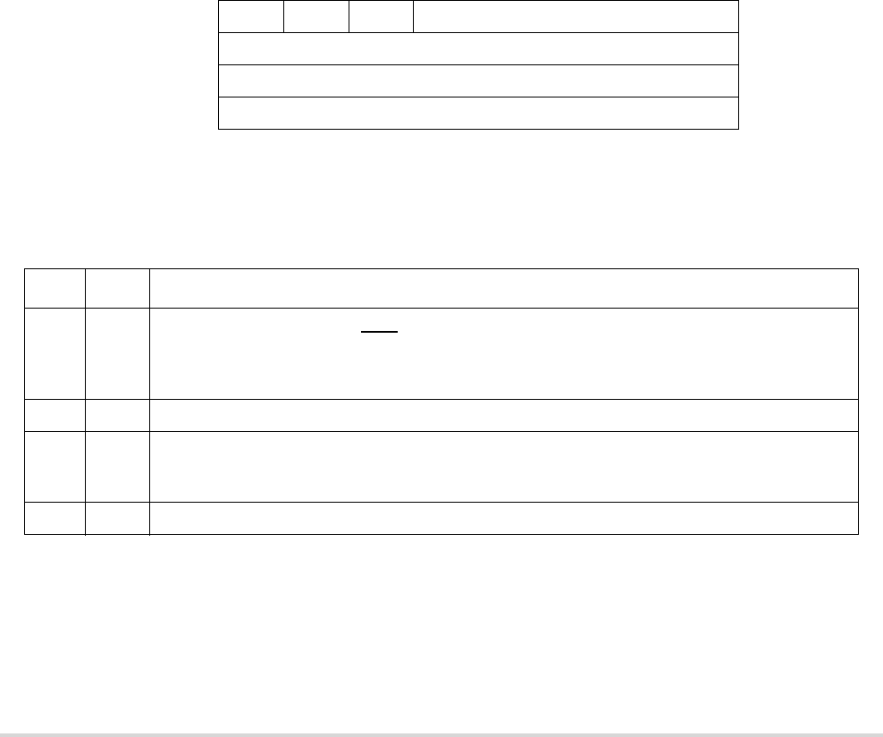
8-6 MCF5282 User’s Manual MOTOROLA
Register Descriptions
For details on the processor's view of the local SRAM memories, see Section 5.3.1,
“SRAM Base Address Register (RAMBAR).”
8.4.3 Core Reset Status Register (CRSR)
The CRSR contains a bit for two of the reset sources to the CPU. A bit set to 1 indicates the
last type of reset that occurred. The CRSR is updated by the control logic when the reset
is complete. Only one bit is set at any one time in the CRSR. The register reflects the cause
of the most recent reset. To clear a bit, a logic 1 must be written to the bit location; writing
a zero has no effect.
NOTE
The reset status register (RSR) in the reset controller module
(see Chapter 28, “Reset Controller Module”) provides
indication of all reset sources except the core watchdog timer.
8.4.4 Core Watchdog Control Register (CWCR)
The core watchdog timer prevents system lockup if the software becomes trapped in a loop
with no controlled exit. The core watchdog timer can be enabled or disabled through
CWCR[CWE]. By default it is disabled. If enabled, the watchdog timer requires the
7654 0
Field EXT — CWDR —
Reset See Note
R/W R/W
Address IPSBAR + 0x010
Note: The reset value of EXT and CWDR depend on the last reset
source. All other bits are initialized to zero.
Figure 8-3. Core Reset Status Register (CRSR)
Table 8-4. CRSR Field Descriptions
Bits Name Description
7 EXT External reset.
1 An external device driving RSTI caused the last reset. Assertion of reset by an external device
causes the processor core to initiate reset exception processing. All registers are forced to their
initial state.
6 — Reserved, should be cleared.
5 CWDR Core watchdog timer reset.
1 The last reset was caused by the core watchdog timer. If CWRI in the CWCR is set and the core
watchdog timer times out, a hard reset occurs.
4–0 — Reserved, should be cleared.

MOTOROLA Chapter 8. System Control Module (SCM) 8-7
Register Descriptions
periodic execution of a core watchdog servicing sequence. If this periodic servicing action
does not occur, the timer times out, resulting in a watchdog timer interrupt or a hardware
reset, as programmed, by CWCR[CWRI]. If the timer times out and the core watchdog
transfer acknowledge enable bit (CWCR[CWTA]) is set, a watchdog timer interrupt is
asserted. If a core watchdog timer interrupt acknowledge cycle has not occurred after
another timeout, CWT TA is asserted in an attempt to allow the interrupt acknowledge
cycle to proceed by terminating the bus cycle. The setting of CWCR[CWTAVAL] indicates
that the watchdog timer TA was asserted.
NOTE
The core watchdog timer is available to provide compatability
with the watchdog timer implemented on previous ColdFire
devices. However, there is a second watchdog timer available
on the MCF5282 that has new features. See Chapter 18,
“Watchdog Timer Module” for more information.
When the core watchdog timer times out and CWCR[CWRI] is programmed for a software
reset, an internal reset is asserted and CRSR[CWDR] is set. To prevent the core watchdog
timer from interrupting or resetting, the CWSR must be serviced by performing the
following sequence:
1. Write 0x55 to CWSR.
2. Write 0xAA to the CWSR.
Both writes must occur in order before the time-out, but any number of instructions can be
executed between the two writes. This order allows interrupts and exceptions to occur, if
necessary, between the two writes. Caution should be exercised when changing CWCR
values after the software watchdog timer has been enabled with the setting of
CWCR[CWE], because it is difficult to determine the state of the core watchdog timer
while it is running. The countdown value is constantly compared with the time-out period
specified by CWCR[CWT]. The following steps must be taken to change CWT:
1. Disable the core watchdog timer by clearing CWCR[CWE].
2. Reset the counter by writing 0x55 and then 0xAA to CWSR.
3. Update CWCR[CWT].
4. Re-enable the core watchdog timer by setting CWCR[CWE]. This step can be
performed in step 3.
The CWCR controls the software watchdog timer, time-out periods, and software watchdog
timer transfer acknowledge. The register can be read at any time, but can be written only if
the CWT is not pending. At system reset, the software watchdog timer is disabled.

8-8 MCF5282 User’s Manual MOTOROLA
Register Descriptions
765 32 1 0
Field CWE CWRI CWT[2:0] CWTA CWTAVAL CWTIC
Reset 0000_0000
R/W R/W
Address IPSBAR + 0x011
Figure 8-4. Core Watchdog Control Register (CWCR)
Table 8-5. CWCR Field Description
Bits Name Description
7 CWE Core watchdog enable.
0 SWT disabled.
1 SWT enabled.
6 CWRI Core watchdog reset/interrupt select.
0 If a time-out occurs, the CWT generates an interrupt to the processor core. The interrupt level for
the CWT is programmed in the interrupt control register 7 (ICR7) of INTC0.
1 A CWT time-out generates a soft reset to the entire device.
5–3 CWT[2:0] Core watchdog timing delay. These bits select the timeout period for the CWT as shown in Table 8-6.
At system reset, the CWT field is cleared signaling the minimum time-out period but the watchdog is
disabled (CWCR[CWE] = 0).
2 CWTA Core watchdog transfer acknowledge enable.
0 CWTA Transfer acknowledge disabled.
1 CWTA Transfer Acknowledge enabled. After one CWT time-out period of the unacknowledged
assertion of the CWT interrupt, the transfer acknowledge asserts, which allows CWT to terminate
a bus cycle and allow the interrupt acknowledge to occur.
1 CWTAVAL Core watchdog transfer acknowledge valid.
0 CWTA Transfer Acknowledge has not occurred.
1 CWTA Transfer Acknowledge has occurred. Write a 1 to clear this flag bit.
0 CWTIF Core watchdog timer interrupt flag.
0 CWT interrupt has not occurred
1 CWT interrupt has occurred. Write a 1 to clear the interrupt request.
Table 8-6. Core Watchdog Timer Delay
CWT [2:0] CWT Time-Out Period
000 29 Bus clock frequency
001 211 Bus clock frequency
010 213 Bus clock frequency
011 215 Bus clock frequency
100 219 Bus clock frequency
101 223 Bus clock frequency
110 227 Bus clock frequency
111 231 Bus clock frequency

MOTOROLA Chapter 8. System Control Module (SCM) 8-9
Internal Bus Arbitration
8.4.5 Core Watchdog Service Register (CWSR)
The software watchdog service sequence must be performed using the CWSR as a data
register to prevent a CWT time-out. The service sequence requires two writes to this data
register: first a write of 0x55 followed by a write of 0xAA. Both writes must be performed
in this order prior to the CWT time-out, but any number of instructions or accesses to the
CWSR can be executed between the two writes. If the CWT has already timed out, writing
to this register has no effect in negating the CWT interrupt. Figure 8-5 illustrates the
CWSR. At system reset, the contents of CWSR are uninitialized.
8.5 Internal Bus Arbitration
The internal bus arbitration is performed by the on-chip bus arbiter, which containing the
arbitration logic that controls which of up to four MBus masters (M0–M3 in Figure 8-6)
has access to the external buses. The function of the arbitration logic is described in this
section.
7 0
Field CWSR[7:0]
Reset Uninitialized
R/W R/W
Address IPSBAR + 0x013
Figure 8-5. Core Watchdog Service Register (CWSR)
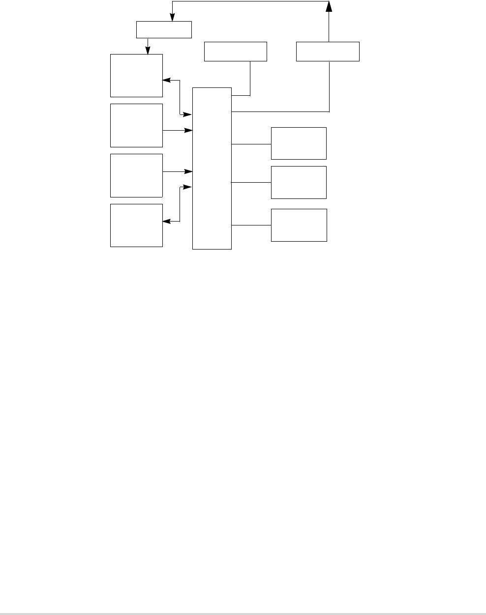
8-10 MCF5282 User’s Manual MOTOROLA
Internal Bus Arbitration
Figure 8-6. Arbiter Module Functions
SRAM1
MPARK RAMBAR
CPU
M0
DMA
M2
Internal
M1
Bus
Master
FEC
M3
EIM
Internal
MARB
Modules
SDRAMC
“back door” to SRAM and Flash

MOTOROLA Chapter 8. System Control Module (SCM) 8-11
Internal Bus Arbitration
8.5.1 Overview
The basic functionality is that of a 4-port, pipelined internal bus arbitration module with the
following attributes:
• The master pointed to by the current arbitration pointer may get on the bus with zero
latency if the address phase is available. All other requesters face at least a one cycle
arbitration pipeline delay in order to meet bus timing constraints on address phase
hold.
• If a requester will get an immediate address phase (that is, it is pointed to by the
current arbitration pointer and the bus address phase is available), it will be the
current bus master and is ignored by arbitration. All remaining requesting ports are
evaluated by the arbitration algorithm to determine the next-state arbitration pointer.
• There are two arbitration algorithms, fixed and round-robin. Fixed arbitration sets
the next-state arbitration pointer to the highest priority requester. Round-robin
arbitration sets the next-state arbitration pointer to the highest priority requester
(calculated by adding a requester's fixed priority to the current bus master’s fixed
priority and then taking this sum modulo the number of possible bus masters).
• The default priority is FEC (M3) > DMA (M2) > internal master (M1) > CPU (M0),
where M3 is the highest and M0 the lowest priority.
• There are two actions for an idle arbitration cycle, either leave the current arbitration
pointer as is or set it to the lowest priority requester.
• The anti-lock-out logic for the fixed priority scheme forces the arbitration algorithm
to round-robin if any requester has been held for longer than a specified cycle count.
8.5.2 Arbitration Algorithms
There are two modes of arbitration: fixed and round-robin. This section discusses the
differences between them.
8.5.2.1 Round-Robin Mode
Round-robin arbitration is the default mode after reset. This scheme cycles through the
sequence of masters as specified by MPARK[Mn_PRTY] bits. Upon completion of a
transfer, the master is given the lowest priority and the priority for all other masters is
increased by one.
M3 = 11 M2 =01 M1 = 10 M0 = 00
next +1 M3 = 00 M2 =10 M1 = 11 M0 = 01
next +2 M3 = 01 M2 =11 M1 = 00 M0 = 10
next +3 M3 = 10 M2 =00 M1 = 01 M0 = 11

8-12 MCF5282 User’s Manual MOTOROLA
Internal Bus Arbitration
If no masters are requesting, the arbitration unit must “park”, pointing at one of the masters.
There are two possibilities, park the arbitration unit on the last active master, or park
pointing to the highest priority master. Setting MPARK[PRK_LAST] causes the arbitration
pointer to be parked on the highest priority master. In round-robin mode, programming the
timeout enable and lockout bits MPARK[13,11:8] will have no effect on the arbitration.
8.5.2.2 Fixed Mode
In fixed arbitration the master with highest priority (as specified by the
MPARK[Mn_PRTY] bits) will win the bus. That master will relinquish the bus when all
transfers to that master are complete.
If MPARK[TIMEOUT] is set, a counter will increment for each master for every cycle it is
denied access. When a counter reaches the limit set by MPARK[LCKOUT_TIME], the
arbitration algorithm will be changed to round-robin arbitration mode until all locks are
cleared. The arbitration will then return to fixed mode and the highest priority master will
be granted the bus.
As in round-robin mode, if no masters are requesting, the arbitration pointer will park on
the highest priority master if MPARK[PRK_LAST] is set, or will park on the master which
last requested the bus if cleared.
8.5.3 Bus Master Park Register (MPARK)
The MPARK controls the operation of the system bus arbitration module. The platform bus
master connections are defined as:
• Master 3 (M3): Fast Ethernet Controller
• Master 2 (M2): 4-channel DMA
• Master 1 (M1): Internal Bus Master (not used in normal user operation)
• Master 0 (M0): V2 ColdFire Core
31 26 25 24 23 22 21 20 19 18 17 16
Field — M2_P_EN BCR24BIT M3_PRTY M2_PRTY M0_PRTY M1_PRTY
Reset 0011_0000_1110_0001
R/W R/W
15 14 13 12 11 8 7 0
Field — FIXED TIMEOUT PRKLAST LCKOUT_TIME —
Reset 0000_0000_0000_0000
R/W R/W
Address IPSBAR + 0x01C
Figure 8-7. Default Bus Master Park Register (MPARK)

MOTOROLA Chapter 8. System Control Module (SCM) 8-13
Internal Bus Arbitration
The initial state of the master priorities is M3 > M2 > M1 > M0. System software should
guarantee that the programmed Mn_PRTY fields are unique, otherwise the hardware
defaults to the initial-state priorities.
Table 8-7. MPARK Field Description
Bits Name Description
31–26 — Reserved, should be cleared.
25 M2_P_EN DMA bandwith control enable
0 disable the use of the DMA's bandwidth control to elevate the priority of its bus requests.
1 enable the use of the DMA's bandwidth control to elevate the priority of its bus requests.
24 BCR24BIT Enables the use of 24 bit byte count registers in the DMA module
0 DMA BCRs function as 16 bit counters.
1 DMA BCRs function as 24 bit counters.
23–22 M3_PRTY Master priority level for master 3 (Fast Ethernet Controller)
00 fourth (lowest) priority
01 third priority
10 second priority
11 first (highest) priority
21–20 M2_PRTY Master priority level for master 2 (DMA Controller)
00 fourth (lowest) priority
01 third priority
10 second priority
11 first (highest) priority
19–18 M0_PRTY Master priority level for master 0 (ColdFire Core)
00 fourth (lowest) priority
01 third priority
10 second priority
11 first (highest) priority
17–16 M1_PRTY Master priority level for master 1 (Not used in user mode)
00 fourth (lowest) priority
01 third priority
10 second priority
11 first (highest) priority
15 — Reserved, should be cleared.
14 FIXED Fixed or round robin arbitration
0 round robin arbitration
1 fixed arbitration
13 TIMEOUT Timeout Enable
0 disable count for when a master is locked out by other masters.
1 enable count for when a master is locked out by other masters and allow access when
LCKOUT_TIME is reached.
12 PRKLAST Park on the last active master or highest priority master if no masters are active
0 park on last active master
1 park on highest priority master
11–8 LCKOUT_TIME Lock-out Time. Lock-out time for a master being denied the bus.
The lock out time is defined as 2^ LCKOUT_TIME[3:0].
7–0 — Reserved, should be cleared.

8-14 MCF5282 User’s Manual MOTOROLA
System Access Control Unit (SACU)
NOTE
The M1_PRTY field should not be set for a priority higher than
third (default).
8.6 System Access Control Unit (SACU)
This section details the functionality of the System Access Control Unit (SACU) which
provides the mechanism needed to implement secure bus transactions to the address space
mapped to the internal modules.
8.6.1 Overview
The SACU supports the traditional model of two privilege levels: supervisor and user.
Typically, memory references with the supervisor attribute have total accessibility to all the
resources in the system, while user mode references cannot access system control and
configuration registers. In many systems, the operating system executes in supervisor
mode, while application software executes in user mode.
The SACU further partitions the access control functions into two parts: one control
register defines the privilege level associated with each bus master, and another set of
control registers define the access levels associated with the peripheral modules and the
memory space.
The SACU’s programming model is physically implemented as part of the System Control
Module (SCM) with the actual access control logic included as part of the arbitration
controller. Each bus transaction targeted for the IPS space is first checked to see if its
privilege rights allow access to the given memory space. If the privilege rights are correct,
the access proceeds on the bus. If the privilege rights are insufficient for the targeted
memory space, the transfer is immediately aborted and terminated with an exception, and
the targeted module not accessed.
8.6.2 Features
Each bus transfer can be classified by its privilege level and the reference type. The
complete set of access types includes:
• Supervisor instruction fetch
• Supervisor operand read
• Supervisor operand write
• User instruction fetch
• User operand read
• User operand write
Instruction fetch accesses are associated with the execute attribute.

MOTOROLA Chapter 8. System Control Module (SCM) 8-15
System Access Control Unit (SACU)
It should be noted that while the bus does not implement the concept of reference type (code
versus data) and only supports the user/supervisor privilege level, the reference type
attribute is supported by the system bus. Accordingly, the access checking associated with
both privilege level and reference type is performed in the IPS controller using the
attributes associated with the reference from the system bus.
The SACU partitions the access control mechanisms into three distinct functions:
• Master privilege register (MPR)
— Allows each bus master to be assigned a privilege level:
– Disable the master’s user/supervisor attribute and force to user mode access
– Enable the master’s user/supervisor attribute
— The reset state provides supervisor privilege to the processor core (bus master 0).
— Input signals allow the non-core bus masters to have their user/supervisor
attribute enabled at reset. This is intended to support the concept of a trusted bus
master, and also controls the ability of a bus master to modify the register state
of any of the SACU control registers; that is, only trusted masters can modify the
control registers.
• Peripheral access control registers (PACRs)
— Nine 8-bit registers control access to 17 of the on-chip peripheral modules.
— Provides read/write access rights, supervisor/user privilege levels
• Reset state provides supervisor-only read/write access to these modulesGrouped
peripheral access control registers (GPACR0, GPACR1)
— One single register (GPACR0) controls access to 14 of the on-chip peripheral
modules
— One register (GPACR1) controls access for IPS reads and writes to the Flash
module
— Provide read/write/execute access rights, supervisor/user privilege levels
— Reset state provides supervisor-only read/write access to each of these peripheral
spaces
8.6.3 Memory Map/Register Definition
The memory map for the SACU program-visible registers within the System Control
Module (SCM) is shown in Figure 8-8. The MPR, PACR, and GPACRs are 8 bits in width.
Table 8-8. SACU Register Memory Map
IPSBAR
Offset [31:28] [27:24] [23:20] [19:16] [15:12] [11:8] [7:4] [3:0]
0x020 MPR ——————
0x024 PACR0 PACR1 PACR2 PACR3

8-16 MCF5282 User’s Manual MOTOROLA
System Access Control Unit (SACU)
8.6.3.1 Master Privilege Register (MPR)
The MPR specifies the access privilege level associated with each bus master in the
platform. The register provides one bit per bus master, where bit 3 corresponds to master 3
(Fast Ethernet Controller), bit 2 to master 2 (DMA Controller), bit1 to master 1 (internal
bus master), and bit 0 to master 0 (ColdFire core).
Only trusted bus masters can modify the access control registers. If a non-trusted bus master
attempts to write any of the SACU control registers, the access is aborted with an error
termination and the registers remain unaffected.
The processor core is connected to bus master 0 and is always treated as a trusted bus
master. Accordingly, MPR[0] is forced to 1 at reset.
8.6.3.2 Peripheral Access Control Registers (PACR 0–PACR8)
Access to several on-chip peripherals is controlled by shared peripheral access control
registers. A single PACR defines the access level for each of the two modules. These
0x028 PACR4 — PACR5 PACR6
0x02c PACR7 — PACR8 —
0x030 GPACR0 GPACR1 — —
0x034 — — — —
0x038 — — — —
0x03C — — — —
7 0
Field — MPR[3:0]
Reset 0000_0011
R/W R/W
Address IPSBAR + 0x020
Figure 8-8. Master Privilege Register (MPR)
Table 8-9. MPR[n] Field Descriptions
Bits Name Description
7–4 — Reserved. Should be cleared.
3–0 MPR Each 1-bit field defines the access privilege level of the given bus master n.
0 All bus master accesses are in user mode.
1 All bus master accesses use the sourced user/supervisor attribute.
Table 8-8. SACU Register Memory Map (continued)
IPSBAR
Offset [31:28] [27:24] [23:20] [19:16] [15:12] [11:8] [7:4] [3:0]

MOTOROLA Chapter 8. System Control Module (SCM) 8-17
System Access Control Unit (SACU)
modules only support operand reads and writes. Each PACR follows the format illustrated
in Figure 8-9. For a list of PACRs and the modules that they control, refer to Table 8-12.
76 432 0
Field LOCK1 ACCESS_CTRL1 LOCK0 ACCESS_CTRL0
Reset 0000_0000
R/W R/W
Address IPSBAR + 0x24 + Offset
Figure 8-9. Peripheral Access Control Register (PACRn)
Table 8-10. PACR Field Descriptions
Bits Name Description
7 LOCK1 This bit, when set, prevents subsequent writes to ACCESSCTRL1. Any attempted
write to the PACR generates an error termination and the contents of the register are
not affected. Only a system reset clears this flag.
6–4 ACCESS_CTRL1 This 3-bit field defines the access control for the given platform peripheral.
The encodings for this field are shown in Table 8-11.
3 LOCK0 This bit, when set, prevents subsequent writes to ACCESSCTRL0. Any attempted
write to the PACR generates an error termination and the contents of the register are
not affected. Only a system reset clears this flag.
2–0 ACCESS_CTRL0 This 3-bit field defines the access control for the given platform peripheral.
The encodings for this field are shown in Table 8-11.
Table 8-11. PACR ACCESSCTRL Bit Encodings
Bits Supervisor Mode User Mode
000 Read/Write No Access
001 Read No Access
010 Read Read
011 Read No Access
100 Read/Write Read/Write
101 Read/Write Read
110 Read/Write Read/Write
111 No Access No Access
Table 8-12. Peripheral Access Control Registers (PACRs)
IPSBAR Offset Name
Modules Controlled
ACCESS_CTRL1 ACCESS_CTRL0
0x024 PACR0 SCM SDRAMC
0x025 PACR1 EIM DMA
0x026 PACR2 UART0 UART1
8-18 MCF5282 User’s Manual MOTOROLA
System Access Control Unit (SACU)
At reset, these on-chip modules are configured to have only supervisor read/write access
capabilities. If an instruction fetch access to any of these peripheral modules is attempted,
the IPS bus cycle is immediately terminated with an error.
8.6.3.3 Grouped Peripheral Access Control Registers
(GPACR0 and GPACR1)
The on-chip peripheral space starting at IPSBAR is subdivided into sixteen 64-Mbyte
regions. Each of the first two regions has a unique access control register associated with
it. The other fourteen regions are in reserved space; the access control registers for these
regions are not implemented. Bits [29:26] of the address select the specific GPACRn to be
used for a given reference within the IPS address space. These access control registers are
8 bits in width so that read, write, and execute attributes may be assigned to the given IPS
region.
NOTE
The access control for modules with memory space protected
by PACR0–PACR8 are determined by the PACR0–PACR8
settings. The access control is not affected by GPACR0, even
though the modules are mapped in its 64-Mbyte address space.
0x027 PACR3 UART2 —
0x028 PACR4 I2C QSPI
0x029 — — —
0x02a PACR5 DTIM0 DTIM1
0x02b PACR6 DTIM2 DTIM3
0x02c PACR7 INTC0 INTC1
0x02d — — —
0x02e PACR8 FEC0 —
76–43 0
Field LOCK —ACCESS_CTRL
Reset 0000_0000
Read/Write R/W R R/W
Address IPSBAR + 0x030, IPSBAR + 0x31
Figure 8-10. GPACR Register
Table 8-12. Peripheral Access Control Registers (PACRs) (continued)
IPSBAR Offset Name
Modules Controlled
ACCESS_CTRL1 ACCESS_CTRL0

MOTOROLA Chapter 8. System Control Module (SCM) 8-19
System Access Control Unit (SACU)
At reset, these on-chip modules are configured to have only supervisor read/write access
capabilities. Bit encodings for the ACCESS_CTRL field in the GPACR are shown in
Table 8-14. Table 8-15 shows the memory space protected by the GPACRs and the modules
mapped to these spaces.
Table 8-13. Grouped PeripheralAccess Control Register
(GPACR) Field Descriptions
Bits Name Description
7 LOCK This bit, once set, prevents subsequent writes to the GPACR. Any attempted write to the
GPACR generates an error termination and the contents of the register are not affected.
Only a system reset clears this flag.
6–4 — Reserved, should be cleared.
3–0 ACCESS_CTRL This 4-bit field defines the access control for the given memory region.
The encodings for this field are shown in Table 8-14.
Table 8-14. GPACR ACCESS_CTRL Bit Encodings
Bits Supervisor Mode User Mode
0000 Read / Write No Access
0001 Read No Access
0010 Read Read
0011 Read No Access
0100 Read / Write Read / Write
0101 Read / Write Read
0110 Read / Write Read / Write
0111 No Access No Access
1000 Read / Write / Execute No Access
1001 Read / Execute No Access
1010 Read / Execute Read / Execute
1011 Execute No Access
1100 Read / Write / Execute Read / Write / Execute
1101 Read / Write / Execute Read / Execute
1110 Read / Write Read
1111 Read / Write / Execute Execute

8-20 MCF5282 User’s Manual MOTOROLA
System Access Control Unit (SACU)
Table 8-15. GPACR Address Space
Register Space Protected
(IPSBAR Offset) Modules Protected
GPACR0 0x0000_0000–
0x03FF_FFFF
Ports, CCM, PMM, Reset controller, Clock,
EPORT, WDOG, PIT0–PIT3, QADC, GPTA, GPTB,
FlexCAN, CFM (Control)
GPACR1 0x0400_0000–
0x07FF_FFFF
CFM (Flash module’s backdoor access for
programming or access by a bus master other than
the core)

MOTOROLA Chapter 9. Clock Module 9-1
Chapter 9
Clock Module
The clock module allows the MCF5282 to be configured for one of several clocking
methods. Clocking modes include internal phase-locked loop (PLL) clocking with either an
external clock reference or an external crystal reference supported by an internal crystal
amplifier. The PLL can also be disabled and an external oscillator can be used to clock the
device directly. The clock module contains:
• Crystal amplifier and oscillator (OSC)
• Phase-locked loop (PLL)
• Reduced frequency divider (RFD)
• Status and control registers
• Control logic
9.1 Features
Features of the clock module include:
• 2- to 10-MHz reference crystal oscillator
• Support for low-power modes
• Separate clock out signal
9.2 Modes of Operation
The clock module can be operated in normal PLL mode (default), 1:1 PLL mode, or
external clock mode.
9.2.1 Normal PLL Mode
In normal PLL mode, the PLL is fully programmable. It can synthesize frequencies ranging
from 2x to 9x the reference frequency and has a post divider capable of reducing this
synthesized frequency without disturbing the PLL. The PLL reference can be either a
crystal oscillator or an external clock.

9-2 MCF5282 User’s Manual MOTOROLA
Low-power Mode Operation
9.2.2 1:1 PLL Mode
In 1:1 PLL mode, the PLL synthesizes a frequency equal to the external clock input
reference frequency. The post divider is not active.
9.2.3 External Clock Mode
In external clock mode, the PLL is bypassed, and the external clock is applied to EXTAL.
The resulting operating frequency is equal to the external clock frequency.
9.3 Low-power Mode Operation
This subsection describes the operation of the clock module in low-power and halted modes
of operation. Low-power modes are described in Chapter 7, “Power Management.”
Table 9-1 shows the clock module operation in low-power modes.
Table 9-1. Clock Module Operation in Low-power Modes
During wakeup from a low-power mode, the Flash clock always clocks through at least 16
cycles before the CPU clocks are enabled. This allows the Flash module time to recover
from the low-power mode, and software can immediately resume fetching instructions
from memory.
In wait and doze modes, the system clocks to the peripherals are enabled, and the clocks to
the CPU, Flash, and SRAM are stopped. Each module can disable its clock locally at the
module level.
In stop mode, all system clocks are disabled. There are several options for enabling or
disabling the PLL or crystal oscillator in stop mode, compromising between stop mode
current and wakeup recovery time. The PLL can be disabled in stop mode, but requires a
wakeup period before it can relock. The oscillator can also be disabled during stop mode,
but requires a wakeup period to restart.
When the PLL is enabled in stop mode (STPMD[1:0]), the external CLKOUT signal can
support systems using CLKOUT as the clock source.
Low-power Mode Clock Operation Mode Exit
Wait Clocks sent to peripheral modules only Exit not caused by clock module, but normal
clocking resumes upon mode exit
Doze Clocks sent to peripheral modules only Exit not caused by clock module, but normal
clocking resumes upon mode exit
Stop All system clocks disabled Exit not caused by clock module, but clock
sources are re-enabled and normal clocking
resumes upon mode exit
Halted Normal Exit not caused by clock module
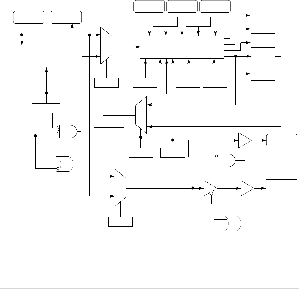
MOTOROLA Chapter 9. Clock Module 9-3
Block Diagram
There is also a fast wakeup option for quickly enabling the system clocks during stop
recovery. This eliminates the wakeup recovery time but at the risk of sending a potentially
unstable clock to the system. To prevent a non-locked PLL frequency overshoot when using
the fast wakeup option, change the RFD divisor to the current RFD value plus one before
entering stop mode.
In external clock mode, there are no wakeup periods for oscillator startup or PLL lock.
9.4 Block Diagram
Figure shows a block diagram of the entire clock module. The PLL block in this diagram
is expanded in detail in Figure 9-2.
.
Figure 9-1. Clock Module Block Diagram
CLKOUT
XTAL
EXTERNAL CLOCK
OSC
PLLREF
REFERENCE
CLOCK
PLL
MFD PLLMODE
LOCEN
CLKMOD[1:0] RSTOUT CLKOUT
LOCKS
LOCK
LOCS
RFD[2:0]
TO RESET
MODULE
LOLRE LOCRE
STPMD[1:0]
STOP MODE
PLLSEL DISCLK
PLL CLOCK OUT
SCALED PLL CLOCK OUT
INTERNAL CLOCK
PLLMODE
CLKGEN
STOP MODE
INTERNAL
CLOCKS
LOCK
FWKUP
EXTAL
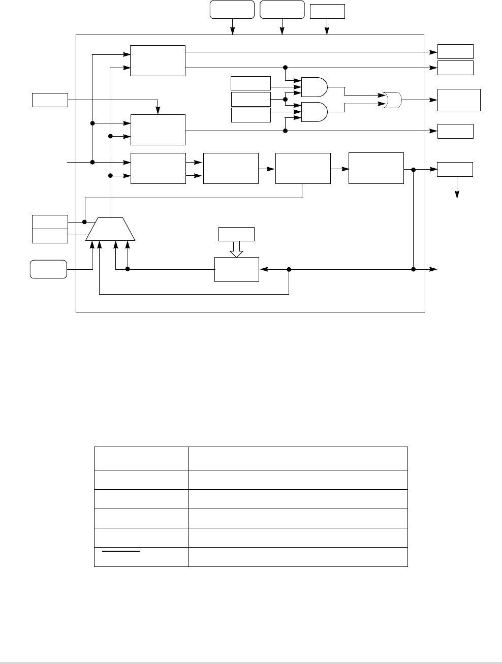
9-4 MCF5282 User’s Manual MOTOROLA
Signal Descriptions
Figure 9-2. PLL Block Diagram
9.5 Signal Descriptions
The clock module signals are summarized in Table 9-2 and a brief description follows. For
more detailed information, refer to Chapter 14, “Signal Descriptions.”
9.5.1 EXTAL
This input is driven by an external clock except when used as a connection to the external
crystal when using the internal oscillator.
Table 9-2. Signal Properties
Name Function
EXTAL Oscillator or clock input
XTAL Oscillator output
CLKOUT System clock output
CLKMOD[1:0] Clock mode select inputs
RSTOUT Reset signal from reset controller
STPMD
CLKMOD[1:0] RSTOUT
÷ MFD
(4–18)
LOCKS
LOCK
LOCS
TO RESET
MODULE
CLKOUT
PLLSEL
DISCLK MDF[2:0]
PHASE AND
FREQUENCY
DETECT
LOSS OF
CLOCK
DETECT
LOCK
DETECT
CHARGE
PUMP FILTER VCO RFD[2:0]
SCALED PLL
CLOCK OUT
PLL CLOCK
OUT
REFERENCE
CLOCK
LOCEN
LOLRE
PLLMODE
LOCRE

MOTOROLA Chapter 9. Clock Module 9-5
Memory Map and Registers
9.5.2 XTAL
This output is an internal oscillator connection to the external crystal.
9.5.3 CLKOUT
This output reflects the internal system clock.
9.5.4 CLKMOD[1:0]
These inputs are used to select the clock mode during chip configuration.
9.5.5 RSTOUT
The RSTOUT pin is asserted by one of the following:
• Internal system reset signal
• FRCRSTOUT bit in the reset control status register (RCR); see Section 28.4.1,
“Reset Control Register (RCR).”
9.6 Memory Map and Registers
The clock module programming model consists of these registers:
• Synthesizer control register (SYNCR), which defines clock operation
• Synthesizer status register (SYNSR), which reflects clock status
9.6.1 Module Memory Map
Table 9-3. Clock Module Memory Map
IPSBAR Offset Register Name Access 1
1S = CPU supervisor mode access only.
0x0012_0000 Synthesizer Control Register (SYNCR) S
0x0012_0002 Synthesizer Status Register (SYNSR) S

9-6 MCF5282 User’s Manual MOTOROLA
Memory Map and Registers
9.6.2 Register Descriptions
This subsection provides a description of the clock module registers.
9.6.2.1 Synthesizer Control Register (SYNCR)
15 14 13 12 11 10 9 8
Field LOLRE MFD2 MFD1 MFD0 LOCRE RFD2 RFD1 RFD0
Reset 0010_0001
R/W R/W
76 5 4 32 10
Field LOCEN DISCLK FWKUP — STPMD1 STPMD0 — —
Reset 0000_0000
R/W R/W R R/W R
Address IPSBAR + 0x0012_0000
Figure 9-3. Synthesizer Control Register (SYNCR)
Table 9-4. SYNCR Field Descriptions
Bit(s) Name Description
15 LOLRE Loss of lock reset enable. Determines how the system handles a loss of lock indication.
When operating in normal mode or 1:1 PLL mode, the PLL must be locked before
setting the LOLRE bit. Otherwise reset is immediately asserted. To prevent an
immediate reset, the LOLRE bit must be cleared before writing the MFD[2:0] bits or
entering stop mode with the PLL disabled.
1 Reset on loss of lock
0 No reset on loss of lock
Note: In external clock mode, the LOLRE bit has no effect.
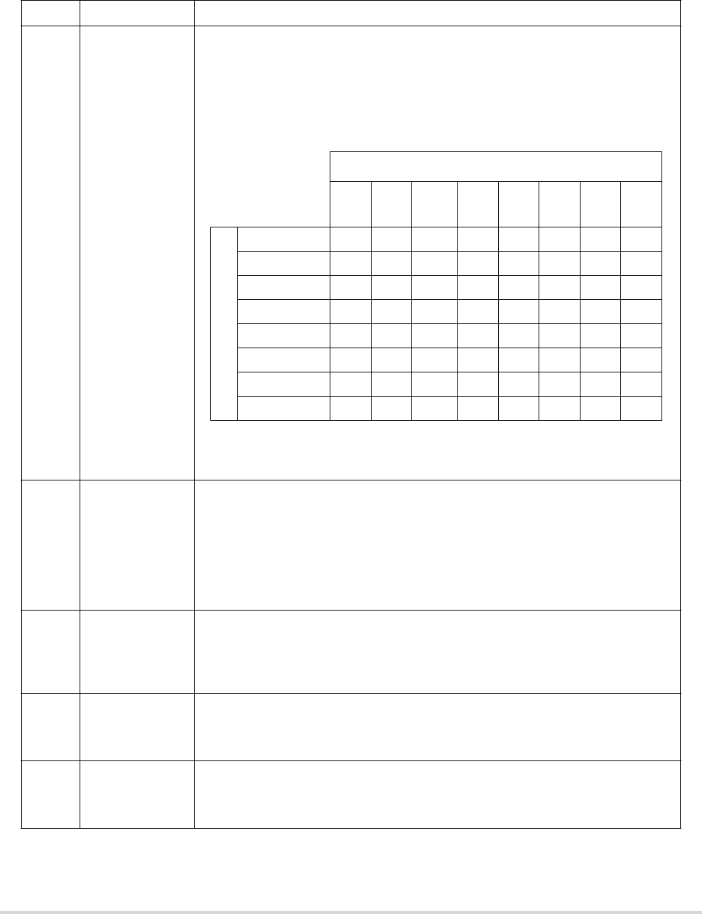
MOTOROLA Chapter 9. Clock Module 9-7
Memory Map and Registers
14–12 MFD Multiplication Factor Divider. Contain the binary value of the divider in the PLL
feedback loop. The MFD[2:0] value is the multiplication factor applied to the reference
frequency. When MFD[2:0] are changed or the PLL is disabled in stop mode, the PLL
loses lock. In 1:1 PLL mode, MFD[2:0] are ignored, and the multiplication factor is one.
Note: In external clock mode, the MFD[2:0] bits have no effect.
11 LOCRE Loss-of-clock reset enable. Determines how the system handles a loss-of-clock
condition. When the LOCEN bit is clear, LOCRE has no effect. If the LOCS flag in
SYNSR indicates a loss-of-clock condition, setting the LOCRE bit causes an
immediate reset. To prevent an immediate reset, the LOCRE bit must be cleared
before entering stop mode with the PLL disabled.
1 Reset on loss-of-clock
0 No reset on loss-of-clock
Note: In external clock mode, the LOCRE bit has no effect.
10–8 RFD Reduced frequency divider field. The binary value written to RFD[2:0] is the PLL
frequency divisor. See table in MFD bit description. Changing RFD[2:0] does not affect
the PLL or cause a relock delay. Changes in clock frequency are synchronized to the
next falling edge of the current system clock. To avoid surpassing the allowable system
operating frequency, write to RFD[2:0] only when the LOCK bit is set.
7 LOCEN Enables the loss-of-clock function. LOCEN does not affect the loss of lock function.
1 Loss-of-clock function enabled
0 Loss-of-clock function disabled
Note: In external clock mode, the LOCEN bit has no effect.
6 DISCLK Disable CLKOUT determines whether CLKOUT is driven. Setting the DISCLK bit holds
CLKOUT low.
1 CLKOUT disabled
0 CLKOUT enabled
Table 9-4. SYNCR Field Descriptions (continued)
Bit(s) Name Description
((
The following table illustrates the system frequency multiplier of the reference
frequency 1 in normal PLL mode.
1fsys = fref x 2(MFD + 2)/2 exp RFD; fref x 2(MFD + 2) ≤ 80 MHz, fsys ≤ 66.67 MHz
MFD[2:0]
000 2
(4x)
2MFD = 000 not valid for fref < 3 MHz
001
(6x)
010
(8x)(3)
011
(10x)
100
(12x)
101
(14x)
110
(16x)
111
(18x)
RFD[2:0]
000 (÷ 1) 4 6 8 1012141618
001 (÷ 2) 3
3Default value out of reset
23 4 56789
010 (÷ 4) 1 3/2 2 5/2 3 7/2 4 9/2
011 (÷ 8) 1/2 3/4 1 5/4 3/2 7/4 2 9/4
100 (÷ 16) 1/4 3/8 1/2 5/8 3/4 7/8 1 9/8
101 (÷ 32) 1/8 3/16 1/4 5/16 3/8 7/16 1/2 9/16
110 (÷ 64) 1/16 3/32 1/8 5/32 3/16 7/32 1/4 9/32
111 (÷ 128) 1/32 3/64 1/16 5/64 3/32 7/64 1/8 9/64
9-8 MCF5282 User’s Manual MOTOROLA
Memory Map and Registers
9.6.2.2 Synthesizer Status Register (SYNSR)
The SYNSR is a read-only register that can be read at any time. Writing to the SYNSR has
no effect and terminates the cycle normally.
5 FWKUP Fast wakeup determines when the system clocks are enabled during wakeup from
stop mode.
1 System clocks enabled on wakeup regardless of PLL lock status
0 System clocks enabled only when PLL is locked or operating normally
Note: When FWKUP = 0, if the PLL or oscillator is enabled and unintentionally lost in
stop mode, the PLL wakes up in self-clocked mode or reference clock mode
depending on the clock that was lost. In external clock mode, the FWKUP bit has no
effect on the wakeup sequence.
4 — Reserved, should be cleared.
3–2 STPMD Control PLL and CLKOUT operation in stop mode. The following table illustrates
STPMD operation in stop mode.
1–0 — Reserved, should be cleared.
76 5 4 32 10
Field PLLMODE PLLSEL PLLREF LOCKS LOCK LOCS —
Reset See note 1 See note 2 000
R/W R
Address IPSBAR + 0x0012_0002
Note: 1. Reset state determined during reset configuration.
2. See the LOCKS and LOCK bit descriptions.
Figure 9-4. Synthesizer Status Register (SYNSR)
Table 9-4. SYNCR Field Descriptions (continued)
Bit(s) Name Description
STPMD[1:0] Operation During Stop Mode
System
Clocks
PLL OSC CLKOUT
00 Disabled Enabled Enabled Enabled
01 Disabled Enabled Enabled Disabled
10 Disabled Disabled Enabled Disabled
11 Disabled Disabled Disabled Disabled

MOTOROLA Chapter 9. Clock Module 9-9
Memory Map and Registers
Table 9-5. SYNSR Field Descriptions
Bit(s) Name Description
7 PLLMODE Clock mode bit. The PLLMODE bit is configured at reset and reflects the clock mode
as shown in Table 9-6.
1 PLL clock mode
0 External clock mode
6 PLLSEL PLL select. Configured at reset and reflects the PLL mode as shown in Table 9-6.
1 Normal PLL mode
0 1:1 PLL mode
5 PLLREF PLL reference. Configured at reset and reflects the PLL reference source in normal
PLL mode as shown in Table 9-6.
1 Crystal clock reference
0 External clock reference
4 LOCKS Sticky indication of PLL lock status.
1 No unintentional PLL loss of lock since last system reset or MFD change
0 PLL loss of lock since last system reset or MFD change or currently not locked due
to exit from STOP with FWKUP set
The lock detect function sets the LOCKS bit when the PLL achieves lock after:
• A system reset
• A write to SYNCR that changes the MFD[2:0] bits
When the PLL loses lock, LOCKS is cleared. When the PLL relocks, LOCKS remains
cleared until one of the two listed events occurs.
In stop mode, if the PLL is intentionally disabled, then the LOCKS bit reflects the value
prior to entering stop mode. However, if FWKUP is set, then LOCKS is cleared until
the PLL regains lock. Once lock is regained, the LOCKS bit reflects the value prior to
entering stop mode. Furthermore, reading the LOCKS bit at the same time that the PLL
loses lock does not return the current loss of lock condition.
In external clock mode, LOCKS remains cleared after reset. In normal PLL mode and
1:1 PLL mode, LOCKS is set after reset.
3 LOCK Set when the PLL is locked. PLL lock occurs when the synthesized frequency is within
approximately 0.75 percent of the programmed frequency. The PLL loses lock when a
frequency deviation of greater than approximately 1.5 percent occurs. Reading the
LOCK flag at the same time that the PLL loses lock or acquires lock does not return
the current condition of the PLL. The power-on reset circuit uses the LOCK bit as a
condition for releasing reset.
If operating in external clock mode, LOCK remains cleared after reset.
1 PLL locked
0 PLL not locked

9-10 MCF5282 User’s Manual MOTOROLA
Functional Description
9.7 Functional Description
This subsection provides a functional description of the clock module.
9.7.1 System Clock Modes
The system clock source is determined during reset (see Table 30-10). The values of
CLKMOD[1:0] are latched during reset and are of no importance after reset is negated. If
CLKMOD1 or CLKMOD0 is changed during a reset other than power-on reset, the internal
clocks may glitch as the system clock source is changed between external clock mode and
PLL clock mode. Whenever CLKMOD1 or CLKMOD0 is changed in reset, an immediate
loss-of-lock condition occurs.
Table 9-7 shows the clockout frequency to clockin frequency relationships for the possible
system clock modes.
2 LOCS Sticky indication of whether a loss-of-clock condition has occurred at any time since
exiting reset in normal PLL and 1:1 PLL modes. LOCS = 0 when the system clocks are
operating normally. LOCS = 1 when system clocks have failed due to a reference
failure or PLL failure.
After entering stop mode with FWKUP set and the PLL and oscillator intentionally
disabled (STPMD[1:0] = 11), the PLL exits stop mode in the SCM while the oscillator
starts up. During this time, LOCS is temporarily set regardless of LOCEN. It is cleared
once the oscillator comes up and the PLL is attempting to lock.
If a read of the LOCS flag and a loss-of-clock condition occur simultaneously, the flag
does not reflect the current loss-of-clock condition.
A loss-of-clock condition can be detected only if LOCEN = 1 or the oscillator has not
yet returned from exit from stop mode with FWKUP = 1.
1 Loss-of-clock detected since exiting reset or oscillator not yet recovered from exit
from stop mode with FWKUP = 1
0 Loss-of-clock not detected since exiting reset
Note: The LOCS flag is always 0 in external clock mode.
1–0 — Reserved, should be cleared.
Table 9-6. System Clock Modes
PLLMODE:PLLSEL:PLLREF Clock Mode
000 External clock mode
100 1:1 PLL mode
110 Normal PLL mode with external clock reference
111 Normal PLL mode with crystal reference
Table 9-5. SYNSR Field Descriptions (continued)
Bit(s) Name Description

MOTOROLA Chapter 9. Clock Module 9-11
Functional Description
CAUTION
XTAL must be tied low in external clock mode when reset is
asserted. If it is not, clocks could be suspended indefinitely.
The external clock is divided by two internally to produce the system clocks.
9.7.2 Clock Operation During Reset
In external clock mode, the system is static and does not recognize reset until a clock is
applied to EXTAL.
In PLL mode, the PLL operates in self-clocked mode (SCM) during reset until the input
reference clock to the PLL begins operating within the limits given in the electrical
specifications.
If a PLL failure causes a reset, the system enters reset using the reference clock. Then the
system clock source changes to the PLL operating in SCM. If SCM is not functional, the
system becomes static. Alternately, if the LOCEN bit in SYNCR is cleared when the PLL
fails, the system becomes static. If external reset is asserted, the system cannot enter reset
unless the PLL is capable of operating in SCM.
9.7.3 System Clock Generation
In normal PLL clock mode, the default system frequency is two times the reference
frequency after reset. The RFD[2:0] and MFD[2:0] bits in the SYNCR select the frequency
multiplier.
When programming the PLL, do not exceed the maximum system clock frequency listed in
the electrical specifications. Use this procedure to accommodate the frequency overshoot
that occurs when the MFD bits are changed:
1. Determine the appropriate value for the MFD and RFD fields in the SYNCR. The
amount of jitter in the system clocks can be minimized by selecting the maximum
MFD factor that can be paired with an RFD factor to provide the required frequency.
2. Write a value of RFD (from step 1) + 1 to the RFD field of the SYNCR.
Table 9-7. Clock Out and Clock In Relationships
System Clock Mode PLL Options 1
1fref = input reference frequency
fsys = CLKOUT frequency
MFD ranges from 0 to 7.
RFD ranges from 0 to 7.
Normal PLL clock mode fsys = fref × 2(MFD + 2)/2RFD
1:1 PLL clock mode fsys = fref
External clock mode fsys = fref
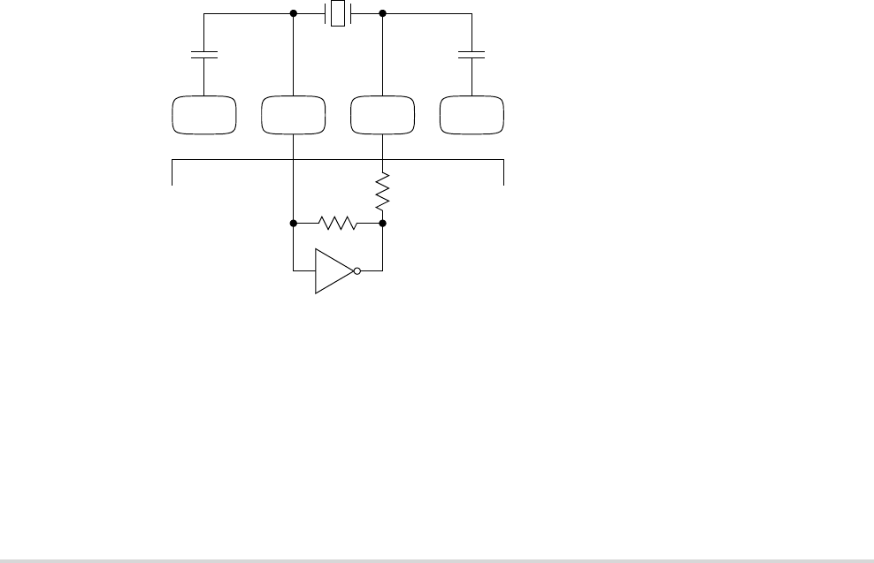
9-12 MCF5282 User’s Manual MOTOROLA
Functional Description
3. Write the MFD value from step 1 to the SYNCR.
4. Monitor the LOCK flag in SYNSR. When the PLL achieves lock, write the RFD
value from step 1 to the RFD field of the SYNCR. This changes the system clocks
frequency to the required frequency.
NOTE
Keep the maximum system clock frequency below the limit
given in the Electrical Characteristics.
9.7.4 PLL Operation
In PLL mode, the PLL synthesizes the system clocks. The PLL can multiply the reference
clock frequency by 2x to 9x, provided that the system clock frequency remains within the
range listed in electrical specifications. For example, if the reference frequency is 2 MHz,
the PLL can synthesize frequencies of 4 MHz to 18 MHz. In addition, the RFD can reduce
the system frequency by dividing the output of the PLL. The RFD is not in the feedback
loop of the PLL, so changing the RFD divisor does not affect PLL operation.
Figure 9-5 shows the external support circuitry for the crystal oscillator with example
component values. Actual component values depend on crystal specifications.
The following subsections describe each major block of the PLL. Refer to Figure to see
how these functional sub-blocks interact.
Figure 9-5. Crystal Oscillator Example
9.7.4.1 Phase and Frequency Detector (PFD)
The PFD is a dual-latch phase-frequency detector. It compares both the phase and
frequency of the reference and feedback clocks. The reference clock comes from either the
crystal oscillator or an external clock source.
VSS VSSSYN
EXTAL XTAL
RS
RF
C1 C2
ON-CHIP
8-MHz CRYSTAL CONFIGURATI
O
C1 = C2 = 16 pF
RF = 1 MΩ
RS = 470 Ω

MOTOROLA Chapter 9. Clock Module 9-13
Functional Description
The feedback clock comes from one of the following:
• CLKOUT in 1:1 PLL mode
• VCO output divided by two if CLKOUT is disabled in 1:1 PLL mode
• VCO output divided by the MFD in normal PLL mode
When the frequency of the feedback clock equals the frequency of the reference clock, the
PLL is frequency-locked. If the falling edge of the feedback clock lags the falling edge of
the reference clock, the PFD pulses the UP signal. If the falling edge of the feedback clock
leads the falling edge of the reference clock, the PFD pulses the DOWN signal. The width
of these pulses relative to the reference clock depends on how much the two clocks lead or
lag each other. Once phase lock is achieved, the PFD continues to pulse the UP and DOWN
signals for very short durations during each reference clock cycle. These short pulses
continually update the PLL and prevent the frequency drift phenomenon known as
dead-banding.
9.7.4.2 Charge Pump/Loop Filter
In 1:1 PLL mode, the charge pump uses a fixed current. In normal mode the current
magnitude of the charge pump varies with the MFD as shown in Table 9-8.
The UP and DOWN signals from the PFD control whether the charge pump applies or
removes charge, respectively, from the loop filter. The filter is integrated on the chip.
9.7.4.3 Voltage Control Output (VCO)
The voltage across the loop filter controls the frequency of the VCO output. The
frequency-to-voltage relationship (VCO gain) is positive, and the output frequency is four
times the target system frequency.
9.7.4.4 Multiplication Factor Divider (MFD)
When the PLL is not in 1:1 PLL mode, the MFD divides the output of the VCO and feeds
it back to the PFD. The PFD controls the VCO frequency via the charge pump and loop
filter such that the reference and feedback clocks have the same frequency and phase. Thus,
the frequency of the input to the MFD, which is also the output of the VCO, is the reference
frequency multiplied by the same amount that the MFD divides by. For example, if the
MFD divides the VCO frequency by six, the PLL is frequency locked when the VCO
Table 9-8. Charge Pump Current and MFD in Normal Mode Operation
Charge Pump Current MFD
1X 0 ≤ MFD < 2
2X 2 ≤ MFD < 6
4X 6 ≤ MFD

9-14 MCF5282 User’s Manual MOTOROLA
Functional Description
frequency is six times the reference frequency. The presence of the MFD in the loop allows
the PLL to perform frequency multiplication, or synthesis.
In 1:1 PLL mode, the MFD is bypassed, and the effective multiplication factor is one.
9.7.4.5 PLL Lock Detection
The lock detect logic monitors the reference frequency and the PLL feedback frequency to
determine when frequency lock is achieved. Phase lock is inferred by the frequency
relationship, but is not guaranteed. The LOCK flag in the SYNSR reflects the PLL lock
status. A sticky lock flag, LOCKS, is also provided.
The lock detect function uses two counters. One is clocked by the reference and the other
is clocked by the PLL feedback. When the reference counter has counted N cycles, its count
is compared to that of the feedback counter. If the feedback counter has also counted N
cycles, the process is repeated for N + K counts. Then, if the two counters still match, the
lock criteria is relaxed by 1/2 and the system is notified that the PLL has achieved
frequency lock.
After lock is detected, the lock circuit continues to monitor the reference and feedback
frequencies using the alternate count and compare process. If the counters do not match at
any comparison time, then the LOCK flag is cleared to indicate that the PLL has lost lock.
At this point, the lock criteria is tightened and the lock detect process is repeated.
The alternate count sequences prevent false lock detects due to frequency aliasing while the
PLL tries to lock. Alternating between tight and relaxed lock criteria prevents the lock
detect function from randomly toggling between locked and non-locked status due to phase
sensitivities. Figure 9-6 shows the sequence for detecting locked and non-locked
conditions.
In external clock mode, the PLL is disabled and cannot lock.
MOTOROLA Chapter 9. Clock Module 9-15
Functional Description
Figure 9-6. Lock Detect Sequence
9.7.4.6 PLL Loss of Lock Conditions
Once the PLL acquires lock after reset, the LOCK and LOCKS flags are set. If the MFD is
changed, or if an unexpected loss of lock condition occurs, the LOCK and LOCKS flags
are negated. While the PLL is in the non-locked condition, the system clocks continue to
be sourced from the PLL as the PLL attempts to relock. Consequently, during the relocking
process, the system clocks frequency is not well defined and may exceed the maximum
system frequency, violating the system clock timing specifications.
However, once the PLL has relocked, the LOCK flag is set. The LOCKS flag remains
cleared if the loss of lock is unexpected. The LOCKS flag is set when the loss of lock is
caused by changing MFD. If the PLL is intentionally disabled during stop mode, then after
exit from stop mode, the LOCKS flag reflects the value prior to entering stop mode once
lock is regained.
9.7.4.7 PLL Loss of Lock Reset
If the LOLRE bit in the SYNCR is set, a loss of lock condition asserts reset. Reset
reinitializes the LOCK and LOCKS flags. Therefore, software must read the LOL bit in the
reset status register (RSR) to determine if a loss of lock caused the reset. See Section 28.4.2,
“Reset Status Register (RSR).”
To exit reset in PLL mode, the reference must be present, and the PLL must achieve lock.
Count N
Reference Cycles
and Compare
Number of Feedback
Cycles Elapsed
Start
with Tight Lock
Criteria Reference Count
≠ Feedback Count
Loss of Lock Detected
Set Tight Lock Criteria
and Notify System of Loss
of Lock Condition
Count N + K
Reference Cycles
and Compare Number
of Feedback Cycles
Elapsed
Lock Detected.
Set Relaxed Lock
Condition and Notify
System of Lock
Condition
Reference Count
≠ Feedback Count
Reference Count =
Feedback Count = N
In Same Count/Compare Sequence
Reference Count =
Feedback Count = N + K
IN Same Count/Compare Sequence

9-16 MCF5282 User’s Manual MOTOROLA
Functional Description
In external clock mode, the PLL cannot lock. Therefore, a loss of lock condition cannot
occur, and the LOLRE bit has no effect.
9.7.4.8 Loss of Clock Detection
The LOCEN bit in the SYNCR enables the loss of clock detection circuit to monitor the
input clocks to the phase and frequency detector (PFD). When either the reference or
feedback clock frequency falls below the minimum frequency, the loss of clock circuit sets
the sticky LOCS flag in the SYNSR.
NOTE
In external clock mode, the loss of clock circuit is disabled.
9.7.4.9 Loss of Clock Reset
The clock module can assert a reset when a loss of clock or loss of lock occurs. When a
loss-of-clock condition is recognized, reset is asserted if the LOCRE bit in SYNCR is set.
The LOCS bit in SYNSR is cleared after reset. Therefore, the LOC bit must be read in RSR
to determine that a loss of clock condition occurred. LOCRE has no effect in external clock
mode.
To exit reset in PLL mode, the reference must be present, and the PLL must acquire lock.
Reset initializes the clock module registers to a known startup state as described in
Section 9.6, “Memory Map and Registers.”
9.7.4.10 Alternate Clock Selection
Depending on which clock source fails, the loss-of-clock circuit switches the system clocks
source to the remaining operational clock. The alternate clock source generates the system
clocks until reset is asserted. As Table 9-9 shows, if the reference fails, the PLL goes out of
lock and into self-clocked mode (SCM). The PLL remains in SCM until the next reset.
When the PLL is operating in SCM, the system frequency depends on the value in the RFD
field. The SCM system frequency stated in electrical specifications assumes that the RFD
has been programmed to binary 000. If the loss-of-clock condition is due to PLL failure,
the PLL reference becomes the system clocks source until the next reset, even if the PLL
regains and relocks.
Table 9-9. Loss of Clock Summary
Clock
Mode
System Clock Source
Before Failure
Reference Failure Alternate Clock
Selected by LOC Circuit 1 Until Reset
1The LOC circuit monitors the reference and feedback inputs to the PFD. See Figure 9-5.
PLL Failure Alternate Clock
Selected by LOC Circuit Until Reset
PLL PLL PLL self-clocked mode PLL reference
External External clock None NA

MOTOROLA Chapter 9. Clock Module 9-17
Functional Description
A special loss-of-clock condition occurs when both the reference and the PLL fail. The
failures may be simultaneous, or the PLL may fail first. In either case, the reference clock
failure takes priority and the PLL attempts to operate in SCM. If successful, the PLL
remains in SCM until the next reset. If the PLL cannot operate in SCM, the system remains
static until the next reset. Both the reference and the PLL must be functioning properly to
exit reset.
9.7.4.11 Loss of Clock in Stop Mode
Table 9-10 shows the resulting actions for a loss of clock in Stop Mode when the device is
being clocked by the various clocking methods.
Table 9-10. Stop Mode Operation (Sheet 1 of 5)
MODE
In
LOCEN
LOCRE
LOLRE
PLL
OSC
FWKUP
Expected
PLL
Action at
Stop
PLL Action
During Stop
MODE
Out
LOCKSS
LOCK
LOCS
Comments
EXT X X X X X X — — EXT 0 0 0
Lose reference
clock
Stuck ———
NRM 0 0 0 Off Off 0 Lose lock,
f.b. clock,
reference
clock
Regain NRM ‘LK 1 ‘LC
No regain Stuck — — —
NRM X 0 0 Off Off 1 Lose lock,
f.b. clock,
reference
clock
Regain clocks, but
don’t regain lock
SCM–>
unstable
NRM
0–>‘L
K
0–>1 1–>‘L
C
Block LOCS and
LOCKS until
clock and lock
respectively
regain; enter
SCM regardless
of LOCEN bit
until reference
regained
No reference clock
regain
SCM–> 0–> 0–> 1–> Block LOCS and
LOCKS until
clock and lock
respectively
regain; enter
SCM regardless
of LOCEN bit
No f.b. clock
regain
Stuck ———

9-18 MCF5282 User’s Manual MOTOROLA
Functional Description
NRM 0 0 0 Off On 0 Lose lock Regain NRM ‘LK 1 ‘LC Block LOCKS
from being
cleared
Lose reference
clock or no lock
regain
Stuck ———
Lose reference
clock,
regain
NRM ‘LK 1 ‘LC Block LOCKS
from being
cleared
NRM 0 0 0 Off On 1 Lose lock No lock regain Unstable
NRM
0–>‘L
K
0–>1 ‘LC Block LOCKS
until lock
regained
Lose reference
clock or no f.b.
clock regain
Stuck ———
Lose reference
clock, regain
Unstable
NRM
0–>‘L
K
0–>1 ‘LC LOCS not set
because
LOCEN = 0
NRM 0 0 0 On On 0 — — NRM ‘LK 1 ‘LC
Lose lock or clock Stuck — — —
Lose lock, regain NRM 0 1 ‘LC
Lose clock and
lock, regain
NRM 0 1 ‘LC LOCS not set
because
LOCEN = 0
NRM 0 0 0 On On 1 — — NRM ‘LK 1 ‘LC
Lose lock Unstable
NRM
0 0–>1 ‘LC
Lose lock, regain NRM 0 1 ‘LC
Lose clock Stuck — — —
Lose clock, regain
without lock
Unstable
NRM
0 0–>1 ‘LC
Lose clock, regain
with lock
NRM 0 1 ‘LC
NRM X X 1 Off X X Lose lock,
f.b. clock,
reference
clock
RESET RESET — — — Reset
immediately
NRM 0 0 1 On On X — — NRM ‘LK 1 ‘LC
Lose lock or clock RESET — — — Reset
immediately
Table 9-10. Stop Mode Operation (Sheet 2 of 5)
MODE
In
LOCEN
LOCRE
LOLRE
PLL
OSC
FWKUP
Expected
PLL
Action at
Stop
PLL Action
During Stop
MODE
Out
LOCKSS
LOCK
LOCS
Comments

MOTOROLA Chapter 9. Clock Module 9-19
Functional Description
NRM 1 0 0 Off Off 0 Lose lock,
f.b. clock,
reference
clock
Regain NRM ‘LK 1 ‘LC REF not entered
during stop;
SCM entered
during stop only
during oscillator
startup
No regain Stuck — — —
NRM 1 0 0 Off On 0 Lose lock,
f.b. clock
Regain NRM ‘LK 1 ‘LC REF mode not
entered during
stop
No f.b. clock or
lock regain
Stuck ———
Lose reference
clock
SCM 0 0 1 Wakeup without
lock
NRM 1 0 0 Off On 1 Lose lock,
f.b. clock
Regain f.b. clock Unstable
NRM
0–>‘L
K
0–>1 ‘LC REF mode not
entered during
stop
No f.b. clock
regain
Stuck ———
Lose reference
clock
SCM 0 0 1 Wakeup without
lock
NRM 1 0 0 On On 0 — — NRM ‘LK 1 ‘LC
Lose reference
clock
SCM 0 0 1 Wakeup without
lock
Lose f.b. clock REF 0 X 1 Wakeup without
lock
Lose lock Stuck — — —
Lose lock, regain NRM 0 1 ‘LC
NRM 1 0 0 On On 1 — — NRM ‘LK 1 ‘LC
Lose reference
clock
SCM 0 0 1 Wakeup without
lock
Lose f.b. clock REF 0 X 1 Wakeup without
lock
Lose lock Unstable
NRM
0 0–>1 ‘LC
NRM 1 0 1 On On X — — NRM ‘LK 1 ‘LC
Lose lock or clock RESET — — — Reset
immediately
Table 9-10. Stop Mode Operation (Sheet 3 of 5)
MODE
In
LOCEN
LOCRE
LOLRE
PLL
OSC
FWKUP
Expected
PLL
Action at
Stop
PLL Action
During Stop
MODE
Out
LOCKSS
LOCK
LOCS
Comments

9-20 MCF5282 User’s Manual MOTOROLA
Functional Description
NRM 1 1 X Off X X Lose lock,
f.b. clock,
reference
clock
RESET RESET — — — Reset
immediately
NRM 1 1 0 On On 0 — — NRM ‘LK 1 ‘LC
Lose clock RESET — — — Reset
immediately
Lose lock Stuck — — —
Lose lock, regain NRM 0 1 ‘LC
NRM 1 1 0 On On 1 — — NRM ‘LK 1 ‘LC
Lose clock RESET — — — Reset
immediately
Lose lock Unstable
NRM
0 0–>1 ‘LC
Lose lock, regain NRM 0 1 ‘LC
NRM 1 1 1 On On X — — NRM ‘LK 1 ‘LC
Lose clock or lock RESET — — — Reset
immediately
REF 1 0 0 X X X — — REF 0 X 1
Lose reference
clock
Stuck ———
SCM 100OffX 0PLL
disabled
Regain SCM SCM 0 0 1 Wakeup without
lock
SCM 100OffX 1PLL
disabled
Regain SCM SCM 0 0 1
SCM 1 0 0 On On 0 — — SCM 0 0 1 Wakeup without
lock
Lose reference
clock
SCM
Table 9-10. Stop Mode Operation (Sheet 4 of 5)
MODE
In
LOCEN
LOCRE
LOLRE
PLL
OSC
FWKUP
Expected
PLL
Action at
Stop
PLL Action
During Stop
MODE
Out
LOCKSS
LOCK
LOCS
Comments

MOTOROLA Chapter 9. Clock Module 9-21
Functional Description
SCM 1 0 0 OnOn1 — — SCM 0 0 1
Lose reference
clock
SCM
Note:
PLL = PLL enabled during STOP mode. PLL = On when STPMD[1:0] = 00 or 01
OSC = Oscillator enabled during STOP mode. Oscillator is on when STPMD[1:0] = 00, 01, or 10
MODES
NRM = normal PLL crystal clock reference or normal PLL external reference or PLL 1:1 mode. During PLL 1:1 or normal
external reference mode, the oscillator is never enabled. Therefore, during these modes, refer to the OSC = On case
regardless of STPMD values.
EXT=external clock mode
REF=PLL reference mode due to losing PLL clock or lock from NRM mode
SCM=PLL self-clocked mode due to losing reference clock from NRM mode
RESET= immediate reset
LOCKS
‘LK= expecting previous value of LOCKS before entering stop
0–>‘LK= current value is 0 until lock is regained which then will be the previous value before entering stop
0–> = current value is 0 until lock is regained but lock is never expected to regain
LOCS
‘LC=expecting previous value of LOCS before entering stop
1–>‘LC= current value is 1 until clock is regained which then will be the previous value before entering stop
1–> =current value is 1 until clock is regained but CLK is never expected to regain
Table 9-10. Stop Mode Operation (Sheet 5 of 5)
MODE
In
LOCEN
LOCRE
LOLRE
PLL
OSC
FWKUP
Expected
PLL
Action at
Stop
PLL Action
During Stop
MODE
Out
LOCKSS
LOCK
LOCS
Comments

9-22 MCF5282 User’s Manual MOTOROLA
Functional Description

MOTOROLA Chapter 10. Interrupt Controller Modules 10-1
Chapter 10
Interrupt Controller Modules
This section details the functionality for the MCF5282 interrupt controllers (INTC0,
INTC1). The general features of each of the interrupt controller include:
• 63 interrupt sources, organized as:
— 56 fully-programmable interrupt sources
— 7 fixed-level interrupt sources
• Each of the 63 sources has a unique interrupt control register (ICRnx) to define the
software-assigned levels and priorities within the level
• Unique vector number for each interrupt source
• Ability to mask any individual interrupt source, plus global mask-all capability
• Supports both hardware and software interrupt acknowledge cycles
• “Wake-up” signal from low-power stop modes
The 56 fully-programmable and seven fixed-level interrupt sources for each of the two
interrupt controllers on the MCF5282 handle the complete set of interrupt sources from all
of the modules on the device. This section describes how the interrupt sources are mapped
to the interrupt controller logic and how interrupts are serviced.
10.1 68K/ColdFire Interrupt Architecture Overview
Before continuing with the specifics of the MCF5282 interrupt controllers, a brief review
of the interrupt architecture of the 68K/ColdFire family is appropriate.
The interrupt architecture of ColdFire is exactly the same as the M68000 family, where
there is a 3-bit encoded interrupt priority level sent from the interrupt controller to the core,
providing 7 levels of interrupt requests. Level 7 represents the highest priority interrupt
level, while level 1 is the lowest priority. The processor samples for active interrupt
requests once per instruction by comparing the encoded priority level against a 3-bit
interrupt mask value (I) contained in bits 10:8 of the machine’s status register (SR). If the
priority level is greater than the SR[I] field at the sample point, the processor suspends
normal instruction execution and initiates interrupt exception processing. Level 7 interrupts
are treated as non-maskable and edge-sensitive within the processor, while levels 1-6 are
treated as level-sensitive and may be masked depending on the value of the SR[I] field. For

10-2 MCF5282 User’s Manual MOTOROLA
68K/ColdFire Interrupt Architecture Overview
correct operation, the ColdFire requires that, once asserted, the interrupt source remain
asserted until explicitly disabled by the interrupt service routine.
During the interrupt exception processing, the CPU enters supervisor mode, disables trace
mode and then fetches an 8-bit vector from the interrupt controller. This byte-sized operand
fetch is known as the interrupt acknowledge (IACK) cycle with the ColdFire
implementation using a special encoding of the transfer type and transfer modifier
attributes to distinguish this data fetch from a “normal” memory access. The fetched data
provides an index into the exception vector table which contains 256 addresses, each
pointing to the beginning of a specific exception service routine. In particular, vectors 64 -
255 of the exception vector table are reserved for user interrupt service routines. The first
64 exception vectors are reserved for the processor to handle reset, error conditions (access,
address), arithmetic faults, system calls, etc. Once the interrupt vector number has been
retrieved, the processor continues by creating a stack frame in memory. For ColdFire, all
exception stack frames are 2 longwords in length, and contain 32 bits of vector and status
register data, along with the 32-bit program counter value of the instruction that was
interrupted (see Section 2.6, “Exception Stack Frame Definition” for more information on
the stack frame format). After the exception stack frame is stored in memory, the processor
accesses the 32-bit pointer from the exception vector table using the vector number as the
offset, and then jumps to that address to begin execution of the service routine. After the
status register is stored in the exception stack frame, the SR[I] mask field is set to the level
of the interrupt being acknowledged, effectively masking that level and all lower values
while in the service routine. For many peripheral devices, the processing of the IACK cycle
directly negates the interrupt request, while other devices require that request to be
explicitly negated during the processing of the service routine.
For the MCF5282, the processing of the interrupt acknowledge cycle is fundamentally
different than previous 68K/ColdFire cores. In the new approach, all IACK cycles are
directly handled by the interrupt controller, so the requesting peripheral device is not
accessed during the IACK. As a result, the interrupt request must be explicitly cleared in
the peripheral during the interrupt service routine. For more information, see
Section 10.1.1.3, “Interrupt Vector Determination.”
Unlike the M68000 family, all ColdFire processors guarantee that the first instruction of the
service routine is executed before sampling for interrupts is resumed. By making this initial
instruction a load of the SR, interrupts can be safely disabled, if required.
During the execution of the service routine, the appropriate actions must be performed on
the peripheral to negate the interrupt request.
For more information on exception processing, see the ColdFire Programmer’s Reference
Manual at http://www.motorola.com/coldfire

MOTOROLA Chapter 10. Interrupt Controller Modules 10-3
68K/ColdFire Interrupt Architecture Overview
10.1.1 Interrupt Controller Theory of Operation
To support the interrupt architecture of the 68K/ColdFire programming model, the
combined 63 interrupt sources are organized as 7 levels, with each level supporting up to 9
prioritized requests. Consider the priority structure within a single interrupt level (from
highest to lowest priority) as shown in Table 10-1.
The level and priority is fully programmable for all sources except interrupt sources 1–7.
Interrupt source 1–7 (from the Edgeport module) are fixed at the corresponding level’s
midpoint priority. Thus, a maximum of 8 fully-programmable interrupt sources are mapped
into a single interrupt level. The “fixed” interrupt source is hardwired to the given level,
and represents the mid-point of the priority within the level. For the fully-programmable
interrupt sources, the 3-bit level and the 3-bit priority within the level are defined in the
8-bit interrupt control register (ICRnx).
The operation of the interrupt controller can be broadly partitioned into three activities:
• Recognition
• Prioritization
• Vector Determination during IACK
10.1.1.1 Interrupt Recognition
The interrupt controller continuously examines the request sources and the interrupt mask
register to determine if there are active requests. This is the recognition phase.
10.1.1.2 Interrupt Prioritization
As an active request is detected, it is translated into the programmed interrupt level, and the
resulting 7-bit decoded priority level (IRQ[7:1]) is driven out of the interrupt controller.
Table 10-1. Interrupt Priority Within a Level
ICR[2:0] Priority Interrupt
Sources
111 7 (Highest) 8-63
110 6 8-63
101 5 8-63
100 4 8-63
— Fixed Midpoint Priority 1-7
011 3 8-63
010 2 8-63
001 1 8-63
000 0 (Lowest) 8-63

10-4 MCF5282 User’s Manual MOTOROLA
68K/ColdFire Interrupt Architecture Overview
The decoded priority levels from all the interrupt controllers are logically summed together
and the highest enabled interrupt request is then encoded into a 3-bit priority level that is
sent to the processor core during this prioritization phase.
10.1.1.3 Interrupt Vector Determination
Once the core has sampled for pending interrupts and begun interrupt exception processing,
it generates an interrupt acknowledge cycle (IACK). The IACK transfer is treated as a
memory-mapped byte read by the processor, and routed to the appropriate interrupt
controller. Next, the interrupt controller extracts the level being acknowledged from
address bits[4:2], and then determines the highest priority interrupt request active for that
level, and returns the 8-bit interrupt vector for that request to complete the cycle. The 8-bit
interrupt vector is formed using the following algorithm:
For INTC0, vector_number = 64 + interrupt source number
For INTC1, vector_number = 128 + interrupt source number
Recall vector_numbers 0 - 63 are reserved for the ColdFire processor and its internal
exceptions. Thus, the following mapping of bit positions to vector numbers applies for the
INTC0:
if interrupt source 1 is active and acknowledged, then vector_number = 65
if interrupt source 2 is active and acknowledged, then vector_number = 66
...
if interrupt source 8 is active and acknowledged, then vector_number = 72
if interrupt source 9 is active and acknowledged, then vector_number = 73
...
if interrupt source 62 is active and acknowledged, then vector_number = 126
The net effect is a fixed mapping between the bit position within the source to the actual
interrupt vector number.
If there is no active interrupt source for the given level, a special “spurious interrupt” vector
(vector_number = 24) is returned and it is the responsibility of the service routine to handle
this error situation.
Note this protocol implies the interrupting peripheral is not accessed during the
acknowledge cycle since the interrupt controller completely services the acknowledge.
This means the interrupt source must be explicitly disabled in the interrupt service routine.
This design provides unique vector capability for all interrupt requests, regardless of the
“complexity” of the peripheral device.
Vector numbers 64-71, and 91-255 are unused.

MOTOROLA Chapter 10. Interrupt Controller Modules 10-5
Memory Map
10.2 Memory Map
The register programming model for the interrupt controllers is memory-mapped to a
256-byte space. In the following discussion, there are a number of program-visible registers
greater than 32 bits in size. For these control fields, the physical register is partitioned into
two 32-bit values: a register “high” (the upper longword) and a register “low” (the lower
longword). The nomenclature <reg_name>H and <reg_name>L is used to reference these
values.
The registers and their locations are defined in Table 10-3. The offsets listed start from the
base address for each interrupt controller. The base addresses for the interrupt controllers
are listed below:
Table 10-2. Interrupt Controller Base Addresses
Interrupt Controller Number Base Address
INTC0 IPSBAR + 0xC00
INTC1 IPSBAR + 0xD00
Global IACK Registers Space 1
1This address space only contains the SWIACK and L1ACK-L7IACK registers. See Section 10.3.7, “Software
and Level n IACK Registers (SWIACKR, L1IACK–L7IACK)" for more information
IPSBAR + 0xF00
Table 10-3. Interrupt Controller Memory Map
Module Offset Bits[31:24] Bits[23:16] Bits[15:8] Bits[7:0]
0x00 Interrupt Pending Register High (IPRH), [63:32]
0x04 Interrupt Pending Register Low (IPRL), [31:1]
0x08 Interrupt Mask Register High (IMRH), [63:32]
0x0c Interrupt Mask Register Low (IMRL), [31:0]
0x10 Interrupt Force Register High (INTFRCH), [63:32]
0x14 Interrupt Force Register Low (INTFRCL), [31:1]
0x18 IRLR[7:1] IACKLPR[7:0] Reserved
0x1c - 0x3c Reserved
0x40 Reserved ICR01 ICR02 ICR03
0x44 ICR04 ICR05 ICR06 ICR07
0x48 ICR08 ICR09 ICR10 ICR11
0x4c ICR12 ICR13 ICR14 ICR15
0x50 ICR16 ICR17 ICR18 ICR19
0x54 ICR20 ICR21 ICR22 ICR23
0x58 ICR24 ICR25 ICR26 ICR27
0x5C ICR28 ICR29 ICR30 ICR31

10-6 MCF5282 User’s Manual MOTOROLA
Register Descriptions
10.3 Register Descriptions
10.3.1 Interrupt Pending Registers (IPRHn, IPRLn)
The IPRHn and IPRLn registers, Figure 10-1 and Figure 10-2, are each 32 bits in size, and
provide a bit map for each interrupt request to indicate if there is an active request (1 =
active request, 0 = no request) for the given source. The state of the interrupt mask register
does not affect the IPRn. The IPRn is cleared by reset. The IPRn is a read-only register, so
any attempted write to this register is ignored. Bit 0 is not implemented and reads as a zero.
0x60 ICR32 ICR33 ICR34 ICR35
0x64 ICR36 ICR37 ICR38 ICR39
0x68 ICR40 ICR41 ICR42 ICR43
0x6C ICR44 ICR45 ICR46 ICR47
0x70 ICR48 ICR49 ICR50 ICR51
0x74 ICR52 ICR53 ICR54 ICR55
0x78 ICR56 ICR57 ICR58 ICR59
0x7C ICR60 ICR61 ICR62 ICR63
0x80-0xDC Reserved
0xE0 SWIACK Reserved
0xE4 L1IACK Reserved
0xE8 L2IACK Reserved
0xEC L3IACK Reserved
0xF0 L4IACK Reserved
0xF4 L5IACK Reserved
0xF8 L6IACK Reserved
0xFC L7IACK Reserved
Table 10-3. Interrupt Controller Memory Map (continued)
Module Offset Bits[31:24] Bits[23:16] Bits[15:8] Bits[7:0]

MOTOROLA Chapter 10. Interrupt Controller Modules 10-7
Register Descriptions
.
31 16
Field INT[63:48]
Reset 0000_0000_0000_0000
R/W R
15 0
Field INT[47:32]
Reset 0000_0000_0000_0000
R/W R
IPSBAR + 0xC00, 0xD00
Figure 10-1. Interrupt Pending Register High (IPRHn)
Table 10-4. IPRHn Field Descriptions
Bits Name Description
31–0 INT Interrupt pending. Each bit corresponds to an interrupt source. The corresponding IMRHn bit
determines whether an interrupt condition can generate an interrupt. At every system clock, the
IPRHn samples the signal generated by the interrupting source. The corresponding IPRHn bit
reflects the state of the interrupt signal even if the corresponding IMRHn bit is set.
0 The corresponding interrupt source does not have an interrupt pending
1 The corresponding interrupt source has an interrupt pending
31 16
Field INT[31:16]
Reset 0000_0000_0000_0000
R/W R
15 10
Field INT[16:1] —
Reset 0000_0000_0000_0000
R/W R
IPSBAR + 0xC04, 0xD04
Figure 10-2. Interrupt Pending Register Low (IPRLn)
Table 10-5. IPRLn Field Descriptions
Bits Name Description
31–1 INT Interrupt Pending. Each bit corresponds to an interrupt source. The corresponding IMRLn bit
determines whether an interrupt condition can generate an interrupt. At every system clock, the
IPRLn samples the signal generated by the interrupting source. The corresponding IPRLn bit reflects
the state of the interrupt signal even if the corresponding IMRLn bit is set.
0 The corresponding interrupt source does not have an interrupt pending
1 The corresponding interrupt source has an interrupt pending
0 — Reserved, should be cleared.

10-8 MCF5282 User’s Manual MOTOROLA
Register Descriptions
10.3.2 Interrupt Mask Register (IMRHn, IMRLn)
The IMRHn and IMRLn registers are each 32 bits in size and provide a bit map for each
interrupt to allow the request to be disabled (1 = disable the request, 0 = enable the request).
The IMRn is set to all ones by reset, disabling all interrupt requests. The IMRn can be read
and written. A write that sets bit 0 of the IMR forces the other 63 bits to be set, disabling
all interrupt sources, and providing a global mask-all capability.
.
.
31 16
Field INT_MASK[63:48]
Reset 1111_1111_1111_1111
R/W R/W
15 0
Field INT_MASK[47:32]
Reset 1111_1111_1111_1111
R/W R/W
IPSBAR + 0xC08, 0xD08
Figure 10-3. Interrupt Mask Register High (IMRHn)
Table 10-6. IMRHn Field Descriptions
Bits Name Description
31–0 INT_MASK Interrupt mask. Each bit corresponds to an interrupt source. The corresponding IMRHn bit
determines whether an interrupt condition can generate an interrupt. The corresponding
IPRHn bit reflects the state of the interrupt signal even if the corresponding IMRHn bit is set.
0 The corresponding interrupt source is not masked
1 The corresponding interrupt source is masked
31 16
Field INT_MASK[31:16]
Reset 1111_1111_1111_1111
R/W R/W
15 10
Field INT_MASK[16:1] MASKALL
Reset 1111_1111_1111_1111
R/W R/W
IPSBAR + 0xC0C, 0xD0C
Figure 10-4. Interrupt Mask Register Low (IMRLn)

MOTOROLA Chapter 10. Interrupt Controller Modules 10-9
Register Descriptions
10.3.3 Interrupt Force Registers (INTFRCHn, INTFRCLn)
The INTFRCHn and INTFRCLn registers are each 32 bits in size and provide a mechanism
to allow software generation of interrupts for each possible source for functional or debug
purposes. The system design may reserve one or more sources to allow software to
self-schedule interrupts by forcing one or more of these bits (1 = force request, 0 = negate
request) in the appropriate INTFRCn register. The assertion of an interrupt request via the
INTFRCn register is not affected by the interrupt mask register. The INTFRCn register is
cleared by reset.
Table 10-7. IMRLn Field Descriptions
Bits Name Description
31–1 INT_MASK Interrupt mask. Each bit corresponds to an interrupt source. The corresponding
IMRLn bit determines whether an interrupt condition can generate an interrupt.
The corresponding IPRLn bit reflects the state of the interrupt signal even if the
corresponding IMRLn bit is set.
0 The corresponding interrupt source is not masked
1 The corresponding interrupt source is masked
0 MASKALL Mask all interrupts. Setting this bit will force the other 63 bits of the IMRHn and
IMRLn to ones, disabling all interrupt sources, and providing a global mask-all
capability.
31 16
Field INTFRCH[63:48]
Reset 0000_0000_0000_0000
R/W R/W
15 0
Field INTFRCH[47:32]
Reset 0000_0000_0000_0000
R/W R/W
IPSBAR + 0xC10, 0xD10
Figure 10-5. Interrupt Force Register High (INTFRCHn)
Table 10-8. INTFRCHn Field Descriptions
Bits Name Description
31–0 INTFRC Interrupt force. Allows software generation of interrupts for each possible source for functional or
debug purposes.
0 No interrupt forced on corresponding interrupt source
1 Force an interrupt on the corresponding source

10-10 MCF5282 User’s Manual MOTOROLA
Register Descriptions
.
10.3.4 Interrupt Request Level Register (IRLRn)
This 7-bit register is updated each machine cycle and represents the current interrupt
requests for each interrupt level, where bit 7 corresponds to level 7, bit 6 to level 6, etc. This
register output is combined with similar outputs from INTC1 and eventually encoded into
the 3-bit priority interrupt level driven to the processor core.
31 16
Field INTFRCL[31:16]
Reset 0000_0000_0000_0000
R/W R
15 10
Field INTFRCL[16:1] —
Reset 0000_0000_0000_0000
R/W R
IPSBAR + 0xC14, 0xD14
Figure 10-6. Interrupt Force Register Low (INTFRCLn)
Table 10-9. INTFRCLn Field Descriptions
Bits Name Description
31–1 INTFRC Interrupt force. Allows software generation of interrupts for each possible source for functional or
debug purposes.
0 No interrupt forced on corresponding interrupt source
1 Force an interrupt on the corresponding source
0 — Reserved, should be cleared.
7 210
Field IRQ[7:1] —
Reset 0000_0000
R/W R
Address IPSBAR + 0xC18, 0xD18
Figure 10-7. Interrupt RequestLevel Register (IRLRn)
Table 10-10. IRQn Field Descriptions
Bits Name Description
7–1 IRQ Interrupt requests. Represents the prioritized active interrupts for each level.
0 There are no active interrupts at this level
1 There is an active interrupt at this level
0—Reserved

MOTOROLA Chapter 10. Interrupt Controller Modules 10-11
Register Descriptions
10.3.5 Interrupt Acknowledge Level and Priority
Register (IACKLPRn)
Each time an IACK is performed, the interrupt controller responds with the vector number
of the highest priority source within the level being acknowledged. In addition to providing
the vector number directly for the byte-sized IACK read, this 8-bit register is also loaded
with information about the interrupt level and priority being acknowledged. This register
provides the association between the acknowledged “physical” interrupt request number
and the programmed interrupt level/priority. The contents of this read-only register are
described in Figure 10-8 and Table 10-11.
10.3.6 Interrupt Control Register (ICRnx, (x = 1, 2,..., 63))
Each ICRnx specifies the interrupt level (1-7) and the priority within the level (0-7). All
ICRnx registers can be read, but only ICRn8 to ICRn63 can be written. It is software’s
responsibility to program the ICRnx registers with unique and non-overlapping level and
priority definitions. Failure to program the ICRnx registers in this manner can result in
undefined behavior. If a specific interrupt request is completely unused, the ICRnx value
can remain in its reset (and disabled) state.
76 43 0
Field — LEVEL PRI
Reset 0000_0000
R/W R
Address IPSBAR + 0xC19, 0xD19
Figure 10-8. IACK Level and Priority Register (IACKLPRn)
Table 10-11. IACKLPRn Field Descriptions
Bits Name Description
7—Reserved
6–4 LEVEL Interrupt level. Represents the interrupt level currently being acknowledged.
3–0 PRI Interrupt Priority. Represents the priority within the interrupt level of the interrupt currently being
acknowledged.
0 Priority 0
1 Priority 1
2 Priority 2
3 Priority 3
4 Priority 4
5 Priority 5
6 Priority 6
7 Priority 7
8 Mid-Point Priority associated with the fixed level interrupts only

10-12 MCF5282 User’s Manual MOTOROLA
Register Descriptions
10.3.6.1 Interrupt Sources
Table 10-13 and Table 10-14 list the interrupt sources for each interrupt request line for
INTC0 and INTC1.
765320
Field — IL IP
Reset 0000_0000
R/W R/W (Read only for ICRn1-ICRn7)
Address See Table 10-2 and Table 10-3 for register offsets
Figure 10-9. Interrupt Control Register (ICRnx)
Table 10-12. ICRnx Field Descriptions
Bits Name Description
7–6 — Reserved, should be cleared.
5–3 IL Interrupt level. Indicates the interrupt level assigned to each interrupt input.
2–0 IP Interrupt priority. Indicates the interrupt priority for internal modules within the interrupt-level
assignment. 000b represents the lowest priority and 111b represents the highest. For the fixed level
interrupt sources, the priority is fixed at the midpoint for the level, and the IP field will always read as
000b.
Table 10-13. Interrupt Source Assignment for INTC0
Source Module Flag Source Description Flag Clearing Mechanism
1 EPORT EPF1 Edge port flag 1 Write EPF1 = 1
2 EPF2 Edge port flag 2 Write EPF2 = 1
3 EPF3 Edge port flag 3 Write EPF3 = 1
4 EPF4 Edge port flag 4 Write EPF4 = 1
5 EPF5 Edge port flag 5 Write EPF5 = 1
6 EPF6 Edge port flag 6 Write EPF6 = 1
7 EPF7 Edge port flag 7 Write EPF7 = 1
8 SCM SWT1 Software watchdog timeout Cleared when service complete
9 DMA DONE DMA Channel 0 transfer complete Write DONE = 1
10 DONE DMA Channel 1 transfer complete Write DONE = 1
11 DONE DMA Channel 2 transfer complete Write DONE = 1
12 DONE DMA Channel 3 transfer complete Write DONE = 1
13 UART0 Multiple UART0 interrupt Cleared when service complete
14 UART1 Multiple UART1 interrupt Cleared when service complete
15 UART2 Multiple UART2 interrupt Cleared when service complete

MOTOROLA Chapter 10. Interrupt Controller Modules 10-13
Register Descriptions
16 Not used
17 I2CIIFI
2C interrupt Write IIF = 0
18 QSPI Multiple QSPI interrupt See QIR description
19 DTIM0 CAP/REF DTIM0 capture/reference event Write CAP = 1 or REF = 1
20 DTIM1 CAP/REF DTIM1 capture/reference event Write CAP = 1 or REF = 1
21 DTIM2 CAP/REF DTIM2 capture/reference event Write CAP = 1 or REF = 1
22 DTIM3 CAP/REF DTIM3 capture/reference event Write CAP = 1 or REF = 1
23 FEC X_INTF Transmit frame interrupt Write X_INTF = 1
24 X_INTB Transmit buffer interrupt Write X_INTB = 1
25 UN Transmit FIFO underrun Write UN = 1
26 RL Collision retry limit Write RL = 1
27 R_INTF Receive frame interrupt Write R_INTF = 1
28 R_INTB Receive buffer interrupt Write R_INTB = 1
29 MII MII interrupt Write MII = 1
30 LC Late collision Write LC = 1
31 HBERR Heartbeat error Write HBERR = 1
32 GRA Graceful stop complete Write GRA = 1
33 EBERR Ethernet bus error Write EBERR = 1
34 BABT Babbling transmit error Write BABT = 1
35 BABR Babbling receive error Write BABR = 1
36 PMM LVDF LVD Write LVDF = 1
37 QADC CF1 Queue 1 conversion complete Write CF1 = 0 after reading CF1 = 1
38 CF2 Queue 2 conversion complete Write CF2 = 0 after reading CF2 = 1
39 PF1 Queue 1 conversion pause Write PF1 = 0 after reading PF1 = 1
40 PF2 Queue 2 conversion pause Write PF2 = 0 after reading PF2 = 1
41 GPTA TOF Timer overflow Write TOF = 1 or access TIMCNTH/L if TFFCA = 1
42 PAIF Pulse accumulator input Write PAIF = 1 or access PAC if TFFCA = 1
43 PAOVF Pulse accumulator overflow Write PAOVF = 1 or access PAC if TFFCA = 1
44 C0F Timer channel 0 Write C0F = 1 or access IC/OC if TFFCA = 1
45 C1F Timer channel 1 Write C1F = 1 or access IC/OC if TFFCA = 1
46 C2F Timer channel 2 Write C2F = 1 or access IC/OC if TFFCA = 1
47 C3F Timer channel 3 Write C3F = 1 or access IC/OC if TFFCA = 1
Table 10-13. Interrupt Source Assignment for INTC0 (continued)
Source Module Flag Source Description Flag Clearing Mechanism

10-14 MCF5282 User’s Manual MOTOROLA
Register Descriptions
48 GPTB TOF Timer overflow Write TOF = 1 or access TIMCNTH/L if TFFCA = 1
49 PAIF Pulse accumulator input Write PAIF = 1 or access PAC if TFFCA = 1
50 PAOVF Pulse accumulator overflow Write PAOVF = 1 or access PAC if TFFCA = 1
51 C0F Timer channel 0 Write C0F = 1 or access IC/OC if TFFCA = 1
52 C1F Timer channel 1 Write C1F = 1 or access IC/OC if TFFCA = 1
53 C2F Timer channel 2 Write C2F = 1 or access IC/OC if TFFCA = 1
54 C3F Timer channel 3 Write C3F = 1 or access IC/OC if TFFCA = 1
55 PIT0 PIF PIT interrupt flag Write PIF = 1 of write PMR
56 PIT1 PIF PIT interrupt flag Write PIF = 1 of write PMR
57 PIT2 PIF PIT interrupt flag Write PIF = 1 of write PMR
58 PIT3 PIF PIT interrupt flag Write PIF = 1 of write PMR
59 CFM CBEIF SGFM buffer empty Write CBEIF = 1
60 CFM CCIF SGFM command complete Cleared automatically
61 CFM PVIF Protection violation Cleared automatically
62 CFM AEIF Access error Cleared automatically
63 Not Used
Table 10-13. Interrupt Source Assignment for INTC0 (continued)
Source Module Flag Source Description Flag Clearing Mechanism

MOTOROLA Chapter 10. Interrupt Controller Modules 10-15
Register Descriptions
10.3.7 Software and Level n IACK Registers (SWIACKR,
L1IACK–L7IACK)
The eight IACK registers can be explicitly addressed via the CPU, or implicitly addressed
via a processor-generated interrupt acknowledge cycle during exception processing. In
either case, the interrupt controller’s actions are very similar.
First, consider an IACK cycle to a specific level: that is, a level-n IACK. When this type of
IACK arrives in the interrupt controller, the controller examines all the currently-active
level n interrupt requests, determines the highest priority within the level, and then
responds with the unique vector number corresponding to that specific interrupt source.
The vector number is supplied as the data for the byte-sized IACK read cycle. In addition
to providing the vector number, the interrupt controller also loads the level and priority
number for the level into the IACKLPR register, where it may be retrieved later.
Table 10-14. Interrupt Source Assignment for INTC1
Source Module Flag Source Description Flag Clearing Mechanism
1-7 Not Used
8FLEX
CAN
BUF0I Message buffer 0 interrupt Write BUF0I = 1 after reading BUF0I = 1
9 BUF1I Message buffer 1 interrupt Write BUF1I = 1 after reading BUF1I = 1
10 BUF2I Message buffer 2 interrupt Write BUF2I = 1 after reading BUF2I = 1
11 BUF3I Message buffer 3 interrupt Write BUF3I = 1 after reading BUF3I = 1
12 BUF4I Message buffer 4 interrupt Write BUF4I = 1 after reading BUF4I = 1
13 BUF5I Message buffer 5 interrupt Write BUF5I = 1 after reading BUF5I = 1
14 BUF6I Message buffer 6 interrupt Write BUF6I = 1 after reading BUF6I = 1
15 BUF7I Message buffer 7 interrupt Write BUF7I = 1 after reading BUF7I = 1
16 BUF8I Message buffer 8 interrupt Write BUF8I = 1 after reading BUF8I = 1
17 BUF9I Message buffer 9 interrupt Write BUF9I = 1 after reading BUF9I = 1
18 BUF10I Message buffer 10 interrupt Write BUF10I = 1 after reading BUF10I = 1
19 BUF11I Message buffer 11 interrupt Write BUF11I = 1 after reading BUF11I = 1
20 BUF12I Message buffer 12 interrupt Write BUF12I = 1 after reading BUF12I = 1
21 BUF13I Message buffer 13 interrupt Write BUF13I = 1 after reading BUF13I = 1
22 BUF14I Message buffer 14 interrupt Write BUF14I = 1 after reading BUF14I = 1
23 BUF15I Message buffer 15 interrupt Write BUF15I = 1 after reading BUF15I = 1
24 ERR_INT Error interrupt Read error bits in ESR or write ERR_INT = 0
25 BOFF_INT Bus-off interrupt Write BOFF_INT = 0
26 WAKE_INT Wake-up interrupt Write WAKE_INT = 0
27-63 Not used

10-16 MCF5282 User’s Manual MOTOROLA
Prioritization Between Interrupt Controllers
This interrupt controller design also supports the concept of a software IACK. A software
IACK is a useful concept that allows an interrupt service routine to determine if there are
other pending interrupts so that the overhead associated with interrupt exception processing
(including machine state save/restore functions) can be minimized. In general, the software
IACK is performed near the end of an interrupt service routine, and if there are additional
active interrupt sources, the current interrupt service routine (ISR) passes control to the
appropriate service routine, but without taking another interrupt exception.
When the interrupt controller receives a software IACK read, it returns the vector number
associated with the highest level, highest priority unmasked interrupt source for that
interrupt controller. The IACKLPR register is also loaded as the software IACK is
performed. If there are no active sources, the interrupt controller returns an all-zero vector
as the operand. For this situation, the IACKLPR register is also cleared.
In addition to the software IACK registers within each interrupt controller, there are global
software IACK registers. A read from the global SWIACK will return the vector number
for the highest level and priority unmasked interrupt source from all interrupt controllers.
A read from one of the LnIACK registers will return the vector for the highest priority
unmasked interrupt within a level for all interrupt controllers.
10.4 Prioritization Between Interrupt Controllers
The interrupt controllers have a fixed priority, where INTC0 has the highest priority, and
INTC1 has the lowest priority. If both interrupt controllers have active interrupts at the
same level and priority, then the INTC0 interrupt will be serviced first. If INTC1 has an
active interrupt that has a higher level or priority than the highest INTC0 interrupt, then the
INTC1 interrupt will be serviced first.
76 43 0
Field VECTOR
Reset 0000_0000
R/W R
Address See Table 10-2 and Table 10-3 for register offsets
Figure 10-10. Software and Level n IACK Registers (SWIACKR, L1IACK–L7IACK)
Table 10-15. SWIACK and L1IACK-L7IACK Field Descriptions
Bits Name Description
7–0 VECTOR Vector number. A read from the SWIACK register returns the vector number associated with the
highest level, highest priority unmasked interrupt source. A read from one of the LnACK registers
returns the highest priority unmasked interrupt source within the level.

MOTOROLA Chapter 10. Interrupt Controller Modules 10-17
Low-Power Wakeup Operation
10.5 Low-Power Wakeup Operation
The System Control Module (SCM) contains an 8-bit low-power interrupt control register
(LPICR) used explicitly for controlling the low-power stop mode. This register must
explicitly be programmed by software to enter low-power mode.
Each interrupt controller provides a special combinatorial logic path to provide a special
wake-up signal to exit from the low-power stop mode. This special mode of operation
works as follows:
• First, LPICR[6:4] is loaded with the mask level that will be specified while the core
is in stop mode. LPICR[7] must be set to enable this mode of operation.
NOTE
The wakeup mask level taken from LPICR[6:4] is adjusted by
hardware to allow a level 7 IRQ to generate a wakeup. That is,
the wakeup mask value used by the interrupt controller must be
in the range of 0–6.
• Second, the processor executes a STOP instruction which places it in stop mode.
Once the processor is stopped, each interrupt controller enables a special logic path
which evaluates the incoming interrupt sources in a purely combinatorial path; that
is, there are no clocked storage elements. If an active interrupt request is asserted and
the resulting interrupt level is greater than the mask value contained in LPICR[6:4],
then each interrupt controller asserts the wake-up output signal, which is routed to
the SCM where it is combined with the wakeup signals from the other interrupt
controller and then to the PLL module to re-enable the device’s clock trees and
resume processing.

10-18 MCF5282 User’s Manual MOTOROLA
Low-Power Wakeup Operation
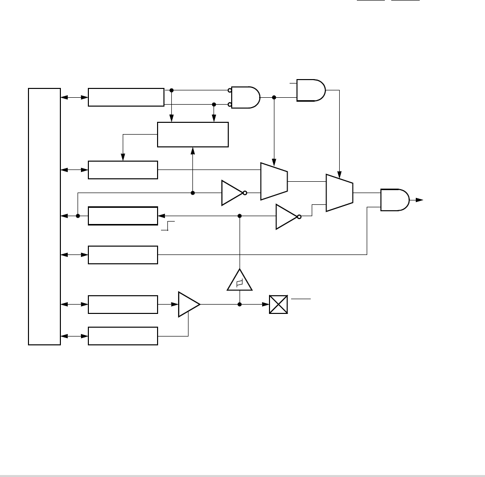
MOTOROLA Chapter 11. Edge Port Module (EPORT) 11-1
Chapter 11
Edge Port Module (EPORT)
11.1 Introduction
The edge port module (EPORT) has seven external interrupt pins, IRQ7–IRQ1. Each pin
can be configured individually as a level-sensitive interrupt pin, an edge-detecting interrupt
pin (rising edge, falling edge, or both), or a general-purpose input/output (I/O) pin. See
Figure 11-1.
Figure 11-1. EPORT Block Diagram
11.2 Low-Power Mode Operation
This section describes the operation of the EPORT module in low-power modes. For more
information on low-power modes, see Chapter 7, “Power Management.” Table 11-1 shows
EPORT module operation in low-power modes, and describes how this module may exit
from each mode.
IPBUS
Synchronizer
EPDR[n]
EPFR[n]
EPPAR[2n, 2n + 1]
EPIER[n]
Edge Detect
D0
Stop
Logic
EPPDR[n]
D1
QD0
D1
Q
Mode
EPDDR[n]
To Interrupt
Controller
IRQx PIN
Rising Edge
of System Clock

11-2 MCF5282 User’s Manual MOTOROLA
Interrupt/General-Purpose I/O Pin Descriptions
NOTE
The low-power interrupt control register (LPICR) in the
System Control Module specifies the interrupt level at or above
which is needed to bring the device out of a low-power mode.
Table 11-1. Edge Port Module Operation in Low-power Modes
In wait and doze modes, the EPORT module continues to operate as it does in run mode. It
may be configured to exit the low-power modes by generating an interrupt request on either
a selected edge or a low level on an external pin. In stop mode, there are no clocks available
to perform the edge-detect function. Only the level-detect logic is active (if configured) to
allow any low level on the external interrupt pin to generate an interrupt (if enabled) to exit
stop mode.
NOTE
The input pin synchronizer is bypassed for the level-detect
logic since no clocks are available.
11.3 Interrupt/General-Purpose I/O Pin Descriptions
All pins default to general-purpose input pins at reset. The pin value is synchronized to the
rising edge of CLKOUT when read from the EPORT pin data register (EPPDR). The values
used in the edge/level detect logic are also synchronized to the rising edge of CLKOUT.
These pins use Schmitt triggered input buffers which have built in hysteresis designed to
decrease the probability of generating false edge-triggered interrupts for slow rising and
falling input signals.
When a pin is configured as an output, it is driven to a state whose level is determined by
the corresponding bit in the EPORT data register (EPDR). All bits in the EPDR are high at
reset.
Low-power Mode EPORT Operation Mode Exit
Wait Normal Any IRQx Interrupt at or above level in LPICR
Doze Normal Any IRQx Interrupt at or above level in LPICR
Stop Level-sensing Only Any IRQx Interrupt set for level-sensing at or above
level in LPICR

MOTOROLA Chapter 11. Edge Port Module (EPORT) 11-3
Memory Map and Registers
11.4 Memory Map and Registers
This subsection describes the memory map and register structure.
11.4.1 Memory Map
Refer to Table 11-2 for a description of the EPORT memory map. The EPORT has an
IPSBAR offset for base address of 0x0013_0000.
11.4.2 Registers
The EPORT programming model consists of these registers:
• The EPORT pin assignment register (EPPAR) controls the function of each pin
individually.
• The EPORT data direction register (EPDDR) controls the direction of each one of
the pins individually.
• The EPORT interrupt enable register (EPIER) enables interrupt requests for each pin
individually.
• The EPORT data register (EPDR) holds the data to be driven to the pins.
• The EPORT pin data register (EPPDR) reflects the current state of the pins.
• The EPORT flag register (EPFR) individually latches EPORT edge events.
Table 11-2. Edge Port Module Memory Map
IPSBAR
Offset Bits 15–8 Bits 7–0 Access 1
1S = CPU supervisor mode access only. S/U = CPU supervisor or user mode access. User mode accesses to supervisor only
addresses have no effect and result in a cycle termination transfer error.
0x0013_0000 EPORT Pin Assignment Register (EPPAR) S
0x0013_0002 EPORT Data Direction Register (EPDDR) EPORT Interrupt Enable Register (EPIER) S
0x0013_0004 EPORT Data Register (EPDR) EPORT Pin Data Register (EPPDR) S/U
0x0013_0006 EPORT Flag Register (EPFR) Reserved 2
2Writing to reserved address locations has no effect, and reading returns 0s.
S/U
11-4 MCF5282 User’s Manual MOTOROLA
Memory Map and Registers
11.4.2.1 EPORT Pin Assignment Register (EPPAR)
11.4.2.2 EPORT Data Direction Register (EPDDR)
15 14 13 12 11 10 9 8 7 6 5 4 3 2 1 0
Field EPPA7 EPPA6 EPPA5 EPPA4 EPPA3 EPPA2 EPPA1 —
Reset 0000_0000_0000_0000
R/W R/W R
Address IPSBAR + 0x0013_0000, 0x0013_0001
Figure 11-2. EPORT Pin Assignment Register (EPPAR)
Table 11-3. EPPAR Field Descriptions
Bit(s) Name Description
15–2 EPPAx EPORT pin assignment select fields. The read/write EPPAx fields configure EPORT pins for
level detection and rising and/or falling edge detection.
Pins configured as level-sensitive are inverted so that a logic 0 on the external pin represents a
valid interrupt request. Level-sensitive interrupt inputs are not latched. To guarantee that a
level-sensitive interrupt request is acknowledged, the interrupt source must keep the signal
asserted until acknowledged by software. Level sensitivity must be selected to bring the device
out of stop mode with an IRQx interrupt.
Pins configured as edge-triggered are latched and need not remain asserted for interrupt
generation. A pin configured for edge detection can trigger an interrupt regardless of its
configuration as input or output.
Interrupt requests generated in the EPORT module can be masked by the interrupt controller
module. EPPAR functionality is independent of the selected pin direction.
Reset clears the EPPAx fields.
00 Pin IRQx level-sensitive
01 Pin IRQx rising edge triggered
10 Pin IRQx falling edge triggered
11 Pin IRQx both falling edge and rising edge triggered
1–0 — Reserved, should be cleared.
765 43210
Field EPDD7 EPDD6 EPDD5 EPDD4 EPDD3 EPDD2 EPDD1 —
Reset 0000_0000
R/W R/W R
Address IPSBAR + 0x0013_0002
Figure 11-3. EPORT Data Direction Register (EPDDR)

MOTOROLA Chapter 11. Edge Port Module (EPORT) 11-5
Memory Map and Registers
11.4.2.3 Edge Port Interrupt Enable Register (EPIER)
11.4.2.4 Edge Port Data Register (EPDR)
Table 11-4. EPDD Field Descriptions
Bit(s) Name Description
7–1 EPDDx Setting any bit in the EPDDR configures the corresponding pin as an output. Clearing any bit
in EPDDR configures the corresponding pin as an input. Pin direction is independent of the
level/edge detection configuration. Reset clears EPDD7-EPDD1.
To use an EPORT pin as an external interrupt request source, its corresponding bit in EPDDR
must be clear. Software can generate interrupt requests by programming the EPORT data
register when the EPDDR selects output.
1 Corresponding EPORT pin configured as output
0 Corresponding EPORT pin configured as input
0 — Reserved, should be cleared.
765 43210
Field EPIE7 EPIE6 EPIE5 EPIE4 EPIE3 EPIE2 EPIE1 —
Reset 0000_0000
R/W R/W R
Address IPSBAR + 0x0013_0003
Figure 11-4. EPORT Port Interrupt Enable Register (EPIER)
Table 11-5. EPIER Field Descriptions
Bit(s) Name Description
7–1 EPIEx Edge port interrupt enable bits enable EPORT interrupt requests. If a bit in EPIER is set,
EPORT generates an interrupt request when:
• The corresponding bit in the EPORT flag register (EPFR) is set or later becomes set.
• The corresponding pin level is low and the pin is configured for level-sensitive operation.
Clearing a bit in EPIER negates any interrupt request from the corresponding EPORT pin.
Reset clears EPIE7-EPIE1.
1 Interrupt requests from corresponding EPORT pin enabled
0 Interrupt requests from corresponding EPORT pin disabled
0 — Reserved, should be cleared.
765 43210
Field EPD7 EPD6 EPD5 EPD4 EPD3 EPD2 EPD1 —
Reset 1111_1111
R/W R/W R
Address IPSBAR + 0x0013_0004
Figure 11-5. EPORT Port Data Register (EPDR)

11-6 MCF5282 User’s Manual MOTOROLA
Memory Map and Registers
11.4.2.5 Edge Port Pin Data Register (EPPDR)
11.4.2.6 Edge Port Flag Register (EPFR)
Table 11-6. EPDR Field Descriptions
Bit(s) Name Description
7–1 EPDx Edge port data bits. Data written to EPDR is stored in an internal register; if any pin of the port
is configured as an output, the bit stored for that pin is driven onto the pin. Reading EDPR
returns the data stored in the register. Reset sets EPD7-EPD1.
0 — Reserved, should be cleared.
765 43210
Field EPPD7 EPPD6 EPPD5 EPPD4 EPPD3 EPPD2 EPPD1 —
Reset Current pin state 0
R/W R
Address IPSBAR + 0x0013_0005
Figure 11-6. EPORT Port Pin Data Register (EPPDR)
Table 11-7. EPPDR Field Descriptions
Bit(s) Name Description
7–1 EPPDx Edge port pin data bits. The read-only EPPDR reflects the current state of the EPORT pins
IRQ7–IRQ1. Writing to EPPDR has no effect, and the write cycle terminates normally. Reset
does not affect EPPDR.
0 — Reserved, should be cleared.
765 43210
Field EPF7 EPF6 EPF5 EPF4 EPF3 EPF2 EPF1 —
Reset 0000_0000
R/W R/W R
Address IPSBAR + 0x0013_0006
Figure 11-7. EPORT Port Flag Register (EPFR)

MOTOROLA Chapter 11. Edge Port Module (EPORT) 11-7
Memory Map and Registers
Table 11-8. EPFR Field Descriptions
Bit(s) Name Description
7–1 EPFx Edge port flag bits. When an EPORT pin is configured for edge triggering, its corresponding
read/write bit in EPFR indicates that the selected edge has been detected. Reset clears
EPF7-EPF1.
Bits in this register are set when the selected edge is detected on the corresponding pin. A bit
remains set until cleared by writing a 1 to it. Writing 0 has no effect. If a pin is configured as
level-sensitive (EPPARx = 00), pin transitions do not affect this register.
1 Selected edge for IRQx pin has been detected.
0 Selected edge for IRQx pin has not been detected.
0 — Reserved, should be cleared.

11-8 MCF5282 User’s Manual MOTOROLA
Memory Map and Registers

MOTOROLA Chapter 12. Chip Select Module 12-1
Chapter 12
Chip Select Module
This chapter describes the MCF5282 chip select module, including the operation and
programming model of the chip select registers, which include the chip select address,
mask, and control registers.
NOTE
Unless otherwise noted, in this chapter, “clock” refers to the
CLKOUT used for the bus.
12.1 Overview
The following list summarizes the key chip select features:
• Up to seven independent, user-programmable chip select signals (CS[6:0]) that can
interface with external SRAM, PROM, EPROM, EEPROM, Flash, and peripherals
• Address masking for 64-Kbyte to 4-Gbyte memory block sizes
12.2 Chip Select Module Signals
Table 12-1 lists signals used by the chip select module.
Table 12-1. Chip Select Module Signals
Signal Description
Chip Selects
(CS[6:0])
Each CSn can be independently programmed for an address location as well as for masking, port
size, read/write burst capability, wait-state generation, and internal/external termination. Only CS0 is
initialized at reset and may act as an external boot chip select to allow boot ROM to be at an external
address space. Port size for CS0 is configured by the logic levels of D[19:18] when RSTO negates
and RCON is asserted.
Output Enable
(OE)
Interfaces to memory or to peripheral devices and enables a read transfer. It is asserted and negated
on the falling edge of the clock. OE is asserted only when one of the chip selects matches for the
current address decode.
Byte Strobes
BS[3:0]
These signals are individually programmed through the byte-enable mode bit, CSCRn[BEM],
described in Section 12.4.1.3.
These generated signals provide byte data select signals, which are decoded from the transfer size,
A1, and A0 signals in addition to the programmed port size and burstability of the memory accessed,
as Table 12-2 shows.

12-2 MCF5282 User’s Manual MOTOROLA
Chip Select Module Signals
Table 12-2 shows the interaction of the byte-enable/byte-write enables with related signals.
Table 12-2. Byte Enables/Byte Write Enable Signal Settings
Transfer Size Port Size A1 A0
BS3BS2 BS1 BS0
D[31:24] D[23:16] D[15:8] D[7:0]
Byte8-bit000111
010111
100111
110111
16-bit000111
011011
100111
111011
32-bit000111
011011
101101
111110
Word8-bit000111
010111
100111
110111
16-bit000011
100011
32-bit000011
101100
Longword8-bit000111
010111
100111
110111
16-bit000011
100011
32-bit000000
Line8-bit000111
010111
100111
110111
16-bit000011
100011
32-bit000000

MOTOROLA Chapter 12. Chip Select Module 12-3
Chip Select Operation
12.3 Chip Select Operation
Each chip select has a dedicated set of registers for configuration and control.
• Chip select address registers (CSARn) control the base address of the chip select.
See Section 12.4.1.1.
• Chip select mask registers (CSMRn) provide 16-bit address masking and access
control. See Section 12.4.1.2.
• Chip select control registers (CSCRn) provide port size and burst capability
indication, wait-state generation, and automatic acknowledge generation features.
See Section 12.4.1.3.
CS0 is a global chip select after reset and provides relocatable boot ROM capability.
12.3.1 General Chip Select Operation
When a bus cycle is initiated, the MCF5282 first compares its address with the base address
and mask configurations programmed for chip selects 0–6 (configured in CSCR0–CSCR6)
and DRAM blocks 0 and 1 (configured in DACR0 and DACR1). If the driven address
matches a programmed chip select or DRAM block, the appropriate chip select is asserted
or the DRAM block is selected using the specifications programmed in the respective
configuration register. Otherwise, the following occurs:
• If the address and attributes do not match in CSAR or DACR, the MCF5282 runs an
external burst-inhibited bus cycle with a default of external termination on a 32-bit
port.
• Should an address and attribute match in multiple CSCRs, the matching chip select
signals are driven; however, the chip select signals are driven during an external
burst-inhibited bus cycle with external termination on a 32-bit port.
• If the address and attribute match both DACRs or a DACR and a CSAR, the
operation is undefined.
Table 12-3 shows the type of access as a function of match in the CSARs and DACRs.
12-4 MCF5282 User’s Manual MOTOROLA
Chip Select Operation
12.3.1.1 8-, 16-, and 32-Bit Port Sizing
Static bus sizing is programmable through the port size bits, CSCR[PS]. See
Section 12.4.1.3 for more information. Figure 12-1 shows the correspondence between the
data bus and the external byte strobe control lines (BS[3:0]). Note that all byte lanes are
driven, although the state of unused byte lanes is undefined.
Figure 12-1. Connections for External Memory Port Sizes
12.3.1.2 External Boot Chip Select Operation
CS0, the external boot chip select, allows address decoding for boot ROM before system
initialization. Its operation differs from other external chip select outputs after system reset.
After system reset, CS0 is asserted for every external access. No other chip select can be
used until the valid bit, CSMR0[V], is set, at which point CS0 functions as configured and
Table 12-3. Accesses by Matches in CSARs and DACRs
Number of CSCR Matches Number of DACR Matches Type of Access
00External
1 0 Defined by CSAR
Multiple 0 External, burst-inhibited, 32-bit
0 1 Defined by DACRs
1 1 Undefined
Multiple 1 Undefined
0 Multiple Undefined
1 Multiple Undefined
Multiple Multiple Undefined
Byte 0
8-bit port
16-bit port
32-bit port
Byte 1
Byte 2
Byte 3
Byte 0 Byte 1
Byte 2 Byte 3
Byte 0 Byte 1 Byte 2 Byte 3
D[31:24] D[23:16] D[15:8] D[7:0]
External
memory
memory
memory
data bus
BS3 BS2 BS1 BS0
Driven, undefined
Driven, undefined

MOTOROLA Chapter 12. Chip Select Module 12-5
Chip Select Registers
CS[6:1] can be used. At reset, the port size function of the external boot chip select is
determined by the logic levels of the inputs on D[19:18]. Table 12-4 and Table 12-4 list the
various reset encodings for the configuration signals multiplexed with D[19:18].
Provided the required address range is in the chip select address register (CSAR0), CS0 can
be programmed to continue decoding for a range of addresses after the CSMR0[V] is set,
after which the external boot chip select can be restored only by a system reset.
12.4 Chip Select Registers
Table 12-5 shows the chip select register memory map. Reading reserved locations returns
zeros.
Table 12-4. D[19:18] External Boot Chip Select Configuration
D[19:18] Boot Device/Data Port Size
00 Internal (32-bit)
01 External (16-bit)
10 External (8-bit)
11 External (32-bit)
Table 12-5. Chip Select Registers
IPSBAR
Offset [31:24] [23:16] [15:8] [7:0]
0x00_0080 Chip select address register—bank 0 (CSAR0)
[p. 12-6]
Reserved 1
0x00_0084 Chip select mask register—bank 0 (CSMR0) [p. 12-7]
0x00_0088 Reserved1Chip select control register—bank 0 (CSCR0)
[p. 12-8]
0x00_008C Chip select address register—bank 1 (CSAR1)
[p. 12-6]
Reserved1
0x00_0090 Chip select mask register—bank 1 (CSMR1) [p. 12-7]
0x00_0094 Reserved1Chip select control register—bank 1 (CSCR1)
[p. 12-8]
0x00_0098 Chip select address register—bank 2 (CSAR2)
[p. 12-6]
Reserved1
0x00_009C Chip select mask register—bank 2 (CSMR2) [p. 12-7]
0x00_00A0 Reserved1Chip select control register—bank 2 (CSCR2)
[p. 12-8]
0x00_00A4 Chip select address register—bank 3 (CSAR3)
[p. 12-6]
Reserved1
0x00_00A8 Chip select mask register—bank 3 (CSMR3) [p. 12-7]

12-6 MCF5282 User’s Manual MOTOROLA
Chip Select Registers
12.4.1 Chip Select Module Registers
The chip select module is programmed through the chip select address registers
(CSAR0–CSAR6), chip select mask registers (CSMR0–CSMR6), and the chip select
control registers (CSCR0–CSCR6).
12.4.1.1 Chip Select Address Registers (CSAR0–CSAR6)
The CSARs, Figure 12-2, specify the chip select base addresses.
Table 12-6 describes CSAR[BA].
0x00_00AC Reserved1Chip select control register—bank 3 (CSCR3)
[p. 12-8]
0x00_00B0 Chip select address register—bank 4 (CSAR4)
[p. 12-6]
Reserved1
0x00_00B4 Chip select mask register—bank 4 (CSMR4) [p. 12-7]
0x00_00B8 Reserved1Chip select control register—bank 4 (CSCR4)
[p. 12-8]
0x00_00BC Chip select address register—bank 5 (CSAR5)
[p. 12-6]
Reserved1
0x00_00C0 Chip select mask register—bank 5 (CSMR5) [p. 12-7]
0x00_00C4 Reserved1Chip select control register—bank 5 (CSCR5)
[p. 12-8]
0x00_00C8 Chip select address register—bank 6 (CSAR6)
[p. 12-6]
Reserved1
0x00_00CC Chip select mask register—bank 6 (CSMR6) [p. 12-7]
0x00_00D0 Reserved1Chip select control register—bank 6 (CSCR6)
[p. 12-8]
1Addresses not assigned to a register and undefined register bits are reserved for expansion. Write accesses to
these reserved address spaces and reserved register bits have no effect.
15 0
Field BA
Reset Uninitialized
R/W R/W
Address 0x080 (CSAR0); 0x08C (CSAR1); 0x098 (CSAR2); 0x0A4 (CSAR3);
0x0B0 (CSAR4); 0x0BC (CSAR5); 0x0C8 (CSAR6)
Figure 12-2. Chip Select Address Registers (CSARn)
Table 12-5. Chip Select Registers (continued)
IPSBAR
Offset [31:24] [23:16] [15:8] [7:0]
MOTOROLA Chapter 12. Chip Select Module 12-7
Chip Select Registers
12.4.1.2 Chip Select Mask Registers (CSMR0–CSMR6)
The CSMRs, Figure 12-3, are used to specify the address mask and allowable access types
for the respective chip selects.
.
Table 12-7 describes CSMR fields.
Table 12-6. CSARn Field Description
Bits Name Description
15–0 BA Base address. Defines the base address for memory dedicated to chip select CS[6:0]. BA is compared
to bits 31–16 on the internal address bus to determine if chip select memory is being accessed.
31 1615 9876543210
Field BAM — WP — AM C/I SC SD UC UD V
Reset Unitialized 0
R/W R/W
Addr 0x084 (CSMR0); 0x090 (CSMR1); 0x09C (CSMR2); 0x0A8 (CSMR3);
0x0B4 (CSMR4); 0x0C0 (CSMR5); 0x0CC (CSMR6)
Figure 12-3. Chip Select Mask Registers (CSMRn)
Table 12-7. CSMRn Field Descriptions
Bits Name Description
31–16 BAM Base address mask. Defines the chip select block by masking address bits. Setting a BAM bit causes
the corresponding CSAR bit to be ignored in the decode.
0 Corresponding address bit is used in chip select decode.
1 Corresponding address bit is a don’t care in chip select decode.
The block size for CS[6:0] is 2n where n = (number of bits set in respective CSMR[BAM]) + 16.
So, if CSAR0 = 0x0000 and CSMR0[BAM] = 0x0008, CS0 addresses a 128-Kbyte (217 byte) range
from 0x0000–0x1_FFFF.
Likewise, for CS0 to access 32 Mbytes (225 bytes) of address space starting at location 0x0000, and
for CS1 to access 16 Mbytes (224 bytes) of address space starting after the CS0 space, then CSAR0
= 0x0000, CSMR0[BAM] = 0x01FF, CSAR1 = 0x0200, and CSMR1[BAM] = 0x00FF.
8 WP Write protect. Controls write accesses to the address range in the corresponding CSAR. Attempting
to write to the range of addresses for which CSARn[WP] = 1 results in the appropriate chip select
not being selected. No exception occurs.
0 Both read and write accesses are allowed.
1 Only read accesses are allowed.
7 — Reserved, should be cleared.
6 AM Alternate master. When AM = 0 during a DMA access, SC, SD, UC, and UD are don’t cares in the
chip select decode.
12-8 MCF5282 User’s Manual MOTOROLA
Chip Select Registers
12.4.1.3 Chip Select Control Registers (CSCR0–CSCR6)
Each CSCR, shown in Figure 12-4, controls the auto-acknowledge, port size, burst
capability, and activation of each chip select. Note that to support the external boot chip
select, CS0, the CSCR0 reset values differ from the other CSCRs. CS0 allows address
decoding for boot ROM before system initialization.
Figure 12-4. Chip Select Control Registers (CSCRn)
Table 12-8 describes CSCRn fields.
5–1 C/I, SC,
SD, UC,
UD
Address space mask bits. These bits determine whether the specified accesses can occur to the
address space defined by the BAM for this chip select.
C/I CPU space and interrupt acknowledge cycle mask
SC Supervisor code address space mask
SD Supervisor data address space mask
UC User code address space mask
UD User data address space mask
0 The address space assigned to this chip select is available to the specified access type.
1 The address space assigned to this chip select is not available (masked) to the specified access
type. If this address space is accessed, chip select is not activated and a regular external bus
cycle occurs.
Note that if AM = 0, SC, SD, UC, and UD are ignored in the chip select decode on DMA access.
0 V Valid bit. Indicates whether the corresponding CSAR, CSMR, and CSCR contents are valid.
Programmed chip selects do not assert until V is set (except for CS0, which acts as the global chip
select). Reset clears each CSMRn[V].
0 Chip select invalid
1 Chip select valid
15 14 13 10 9 8 7 6 5 4 3 2 0
Field — WS — AA PS1 PS0 BEM BSTR BSTW —
Reset: CSCR0 — 11_11 — 1 D19 D18 — —
Reset: Other CSCRs Uninitialized
R/W R/W
Address 0x08A (CSCR0); 0x096 (CSCR1); 0x0A2 (CSCR2); 0x0AE (CSCR3);
0x0BA (CSCR4); 0x0C6 (CSCR5); 0x0D2 (CSCR6)
Table 12-7. CSMRn Field Descriptions (continued)
Bits Name Description
MOTOROLA Chapter 12. Chip Select Module 12-9
Chip Select Registers
Table 12-8. CSCRn Field Descriptions
Bits Name Description
15–14 — Reserved, should be cleared.
13–10 WS Wait states. The number of wait states inserted before an internal transfer acknowledge is generated
(WS = 0 inserts zero wait states, WS = 0xF inserts 15 wait states). If AA = 0, TA must be asserted by
the external system regardless of the number of wait states generated. In that case, the external
transfer acknowledge ends the cycle. An external TA supercedes the generation of an internal TA.
9 — Reserved, should be cleared.
8 AA Auto-acknowledge enable. Determines the assertion of the internal transfer acknowledge for accesses
specified by the chip select address.
0 No internal TA is asserted. Cycle is terminated externally.
1 Internal TA is asserted as specified by WS. Note that if AA = 1 for a corresponding CSn and the
external system asserts an external TA before the wait-state countdown asserts the internal TA, the
cycle is terminated. Burst cycles increment the address bus between each internal termination.
7–6 PS Port size. Specifies the width of the data associated with each chip select. It determines where data is
driven during write cycles and where data is sampled during read cycles. See Section 12.3.1.1.
00 32-bit port size. Valid data sampled and driven on D[31:0]
01 8-bit port size. Valid data sampled and driven on D[31:24]
1x 16-bit port size. Valid data sampled and driven on D[31:16]
5 BEM Byte enable mode. Specifies the byte enable operation. Certain SRAMs have byte enables that must
be asserted during reads as well as writes. BEM can be set in the relevant CSCR to provide the
appropriate mode of byte enable in support of these SRAMs.
0BS
is not asserted for read. BS is asserted for data write only.
1BS
is asserted for read and write accesses.
4 BSTR Burst read enable. Specifies whether burst reads are used for memory associated with each CSn.
0 Data exceeding the specified port size is broken into individual, port-sized non-burst reads. For
example, a longword read from an 8-bit port is broken into four 8-bit reads.
1 Enables data burst reads larger than the specified port size, including longword reads from 8- and
16-bit ports, word reads from 8-bit ports, and line reads from 8-, 16-, and 32-bit ports.
3 BSTW Burst write enable. Specifies whether burst writes are used for memory associated with each CSn.
0 Break data larger than the specified port size into individual port-sized, non-burst writes. For
example, a longword write to an 8-bit port takes four byte writes.
1 Enables burst write of data larger than the specified port size, including longword writes to 8 and
16-bit ports, word writes to 8-bit ports and line writes to 8-, 16-, and 32-bit ports.
2–0 — Reserved, should be cleared.

12-10 MCF5282 User’s Manual MOTOROLA
Chip Select Registers

MOTOROLA Chapter 13. External Interface Module (EIM) 13-1
Chapter 13
External Interface Module (EIM)
This chapter describes data-transfer operations, error conditions, and reset operations.
Chapter 15, “Synchronous DRAM Controller Module,” describes DRAM cycles.
NOTE:
Unless otherwise noted, in this chapter, “clock” refers to the
CLKOUT used for the bus.
13.1 Features
The following list summarizes bus operation features:
• Up to 24 bits of address and 32 bits of data
• Access 8-, 16-, and 32-bit data port sizes
• Generates byte, word, longword, and line-size transfers
• Burst and burst-inhibited transfer support
• Optional internal termination for external bus cycles
13.2 Bus and Control Signals
Table 13-1 summarizes MCF5282 bus signals described in Chapter 14, “Signal
Descriptions.”
Table 13-1. ColdFire Bus Signal Summary
Signal Name Description I/O CLKOUT Edge
A[23:0] Address bus O Rising
BS 1Byte selects O Falling
CS[6:0] 1Chip selects O Falling
D[31:0] Data bus I/O Rising
OE 1Output enable O Falling
R/W Read/write O Rising
SIZ[1:0] Transfer size O Rising
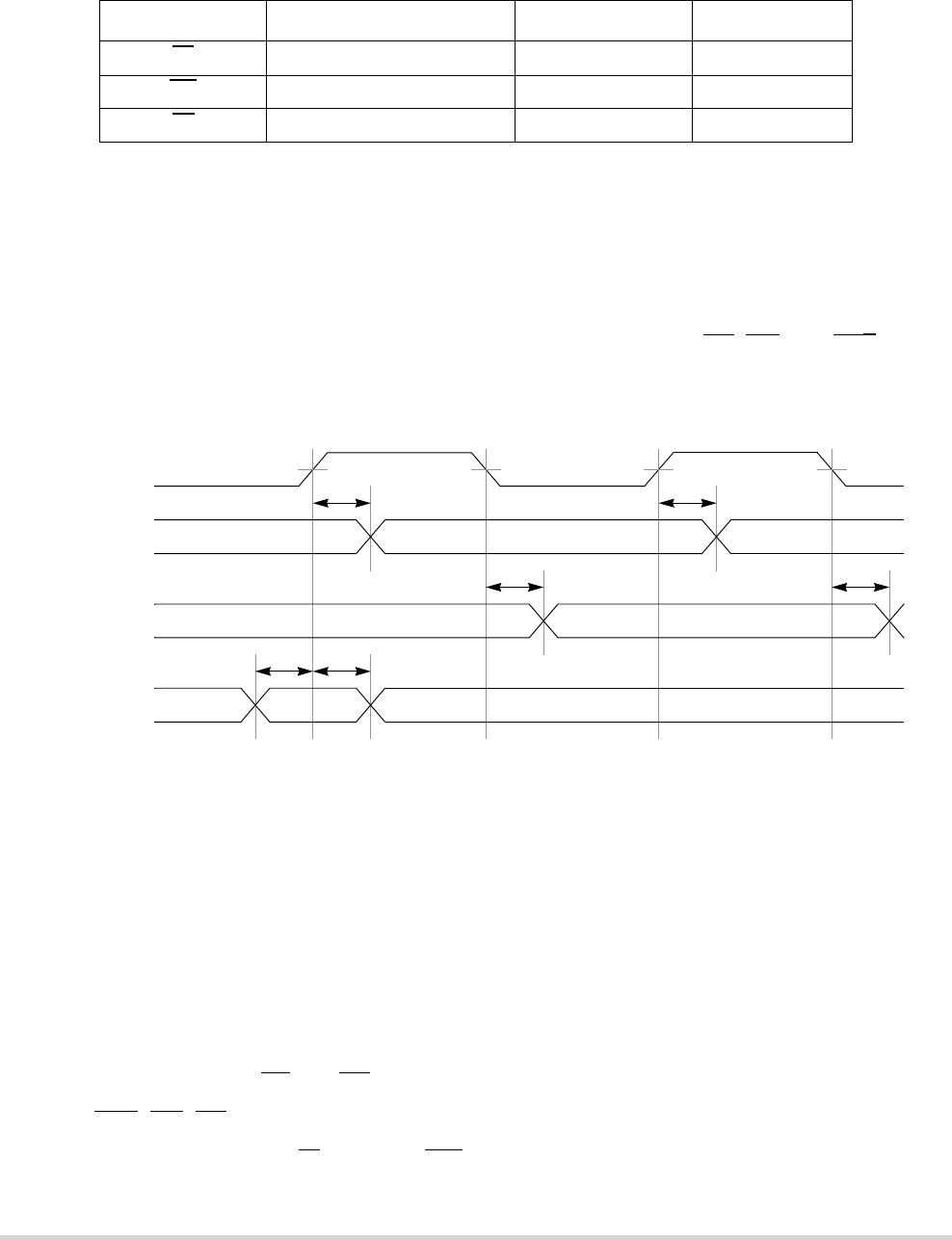
13-2 MCF5282 User’s Manual MOTOROLA
Bus Characteristics
13.3 Bus Characteristics
The MCF5282 uses its system clock to generate CLKOUT. Therefore, the external bus
operates at the same speed as the bus clock rate, where all bus operations are synchronous
to the rising edge of CLKOUT, and some of the bus control signals (BS, OE, and CSn,) are
synchronous to the falling edge, shown in Figure 13-1. Bus characteristics may differ
somewhat for interfacing with external DRAM.
Figure 13-1. Signal Relationship to CLKOUT for Non-DRAM Access
13.4 Data Transfer Operation
Data transfers between the MCF5282 and other devices involve the following signals:
• Address bus (A[23:0])
• Data bus (D[31:0])
• Control signals (TS and TA)
•CS
n, OE, BS
• Attribute signals (R/W, SIZ, and TIP)
TA Transfer acknowledge I Rising
TIP Transfer in progress O Rising
TS Transfer start O Rising
1These signals change after the falling edge. In the Electrical Specifications, these signals
are specified off of the rising edge because CLKIN is squared up internally.
Table 13-1. ColdFire Bus Signal Summary (Continued)
Signal Name Description I/O CLKOUT Edge
Rising-Edge
Signals
Falling-Edge
Signals
Inputs
tvo tho
tvo tho
tsi thi
CLKOUT
tvo = Propagation delay of signal relative to CLKOUT edge
tho = Output hold time relative to CLKOUT edge
tsi = Required input setup time relative to CLKOUT edge
thi = Required input hold time relative to CLKOUT edge
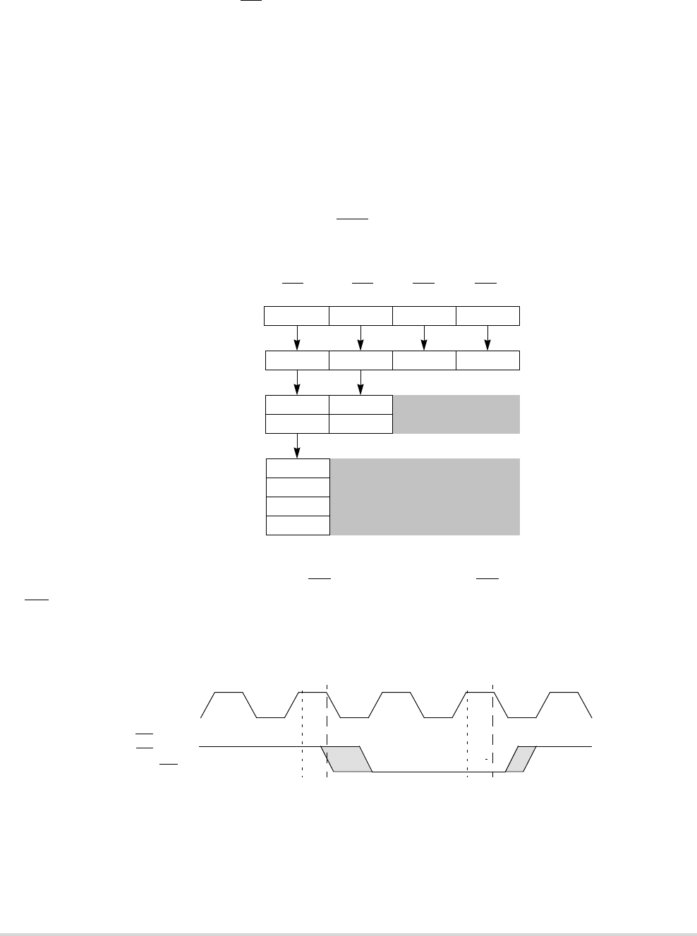
MOTOROLA Chapter 13. External Interface Module (EIM) 13-3
Data Transfer Operation
The address bus, write data, TS, and all attribute signals change on the rising edge of
CLKOUT. Read data is latched into the MCF5282 on the rising edge of CLKOUT.
The MCF5282 bus supports byte, word, and longword operand transfers and allows
accesses to 8-, 16-, and 32-bit data ports. Aspects of the transfer, such as the port size, the
number of wait states for the external slave being accessed, and whether internal transfer
termination is enabled, can be programmed in the chip-select control registers (CSCRs) and
the DRAM control registers (DACRs).
Figure 13-2 shows the byte lanes that external memory should be connected to and the
sequential transfers if a longword is transferred for three port sizes. For example, an 8-bit
memory should be connected to D[31:24] (BS3). A longword transfer takes four transfers
on D[31:24], starting with the MSB and going to the LSB.
Figure 13-2. Connections for External Memory Port Sizes
The timing relationship of chip selects (CS[7:0]), byte selects (BS[3:0]), and output enable
(OE) with respect to CLKOUT is similar in that all transitions occur during the low phase
of CLKOUT. However, due to differences in on-chip signal routing, signals may not assert
simultaneously.
Figure 13-3. Chip-Select Module Output Timing Diagram
13.4.1 Bus Cycle Execution
When a bus cycle is initiated, the MCF5282 first compares the address of that bus cycle
with the base address and mask configurations programmed for chip selects 0–7
Processor
Data Bus
Byte 0
8-Bit Port
16-Bit Port
32-Bit Port
Byte 1
Byte 2
Byte 3
Byte 0 Byte 1
Byte 2 Byte 3
Byte 0 Byte 1 Byte 2 Byte 3
D[31:24] D[23:16] D[15:8] D[7:0]
External
Memory
Memory
Memory
Byte Enable BS3 BS2 BS1 BS0
Driven with
indeterminate values
Driven with
indeterminate values
CS[7:0]
CLKOUT
BS[3:0]
OE
13-4 MCF5282 User’s Manual MOTOROLA
Data Transfer Operation
(configured in CSCR0–CSCR7) and DRAM block 0 and 1 address and control registers
(configured in DACR0 and DACR1). If the driven address compares with one of the
programmed chip selects or DRAM blocks, the appropriate chip select is asserted or the
DRAM block is selected using the specifications programmed by the user in the respective
configuration register. Otherwise, the following occurs:
• If the address and attributes do not match in CSCR or DACR, the MCF5282 runs an
external burst-inhibited bus cycle with a default of external termination on a 32-bit
port.
• Should an address and attribute match in multiple CSCRs, the matching chip-select
signals are driven; however, the MCF5282 runs an external burst-inhibited bus cycle
with external termination on a 32-bit port.
• Should an address and attribute match both DACRs or a DACR and a CSCR, the
operation is undefined.
Table 13-2 shows the type of access as a function of match in the CSCRs and DACRs.
Basic operation of the MCF5282 bus is a three-clock bus cycle.
1. During the first clock, the address, attributes, and TS are driven.
2. Data and TA are sampled during the second clock of a bus-read cycle. During a read,
the external device provides data and is sampled at the rising edge at the end of the
second bus clock. This data is concurrent with TA, which is also sampled at the
rising edge of the clock.
During a write, the ColdFire device drives data from the rising clock edge at the end
of the first clock to the rising clock edge at the end of the bus cycle. Wait states can
be added between the first and second clocks by delaying the assertion of TA. TA
can be configured to be generated internally through the CSCRs. If TA is not
generated internally, the system must provide it externally.
Table 13-2. Accesses by Matches in CSCRs and DACRs
Number of CSCR Matches Number of DACR Matches Type of Access
0 0 External
1 0 Defined by CSCR
Multiple 0 External, burst-inhibited, 32-bit
0 1 Defined by DACRs
1 1 Undefined
Multiple 1 Undefined
0 Multiple Undefined
1 Multiple Undefined
Multiple Multiple Undefined
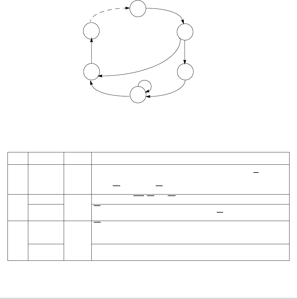
MOTOROLA Chapter 13. External Interface Module (EIM) 13-5
Data Transfer Operation
3. The last clock of the bus cycle uses what would be an idle clock between cycles to
provide hold time for address, attributes and write data. Figure 13-6 and Figure 13-8
show the basic read and write operations.
13.4.2 Data Transfer Cycle States
The data transfer operation in the MCF5282 is controlled by an on-chip state machine. Each
bus clock cycle is divided into two states. Even states occur when CLKOUT is high and
odd states occur when CLKOUT is low. The state transition diagram for basic and fast
termination read and write cycles are shown in Figure 13-4.
Figure 13-4. Data Transfer State Transition Diagram
Table 13-3 describes the states as they appear in subsequent timing diagrams.
Table 13-3. Bus Cycle States
State Cycle CLKOUT Description
S0 All High The read or write cycle is initiated in S0. On the rising edge of CLKOUT, the
MCF5282 places a valid address on the address bus and drives R/W high for a
read and low for a write, if it is not already in the appropriate state. The MCF5282
asserts TIP, SIZ[1:0], and TS on the rising edge of CLKOUT.
S1 All Low The appropriate CSn, BS, and OE signals assert on the CLKOUT falling edge.
Fast
Termination
TA must be asserted during S1. Data is made available by the external device
and is sampled on the rising edge of CLKOUT with TA asserted.
S2 Read/write
(skipped fast
termination)
High TS is negated on the rising edge of CLKOUT in S2.
Write The data bus is driven out of high impedance as data is placed on the bus on the
rising edge of CLKOUT.
S0
S3
S5
S4
S1
S2
Basic
Next Cycle
Wait
States
Read/Write
Fast
Termination
13-6 MCF5282 User’s Manual MOTOROLA
Data Transfer Operation
NOTE:
An external device has at most two CLKOUT cycles after the
start of S4 to three-state the data bus. This applies to basic read
cycles, fast termination cycles, and the last transfer of a burst.
13.4.3 Read Cycle
During a read cycle, the MCF5282 receives data from memory or from a peripheral device.
Figure 13-5 is a read cycle flowchart.
S3 Read/write
(skipped for
fast
termination)
Low The MCF5282 waits for TA assertion. If TA is not sampled as asserted before the
rising edge of CLKOUT at the end of the first clock cycle, the MCF5282 inserts
wait states (full clock cycles) until TA is sampled as asserted.
Read Data is made available by the external device on the falling edge of CLKOUT and
is sampled on the rising edge of CLKOUT with TA asserted.
S4 All High The external device should negate TA.
Read
(including
fast-terminat
ion)
The external device can stop driving data after the rising edge of CLKOUT.
However data could be driven through the end of S5.
S5 S5 Low CS, BS, and OE are negated on the CLKOUT falling edge of S5. The MCF5282
stops driving address lines and R/W on the rising edge of CLKOUT, terminating
the read or write cycle. At the same time, the MCF5282 negates TIP
, and SIZ[1:0]
on the rising edge of CLKOUT.
Note that the rising edge of CLKOUT may be the start of S0 for the next access
cycle.
Read The external device stops driving data between S4 and S5.
Write The data bus returns to high impedance on the rising edge of CLKOUT. The
rising edge of CLKOUT may be the start of S0 for the next access.
Table 13-3. Bus Cycle States (Continued)
State Cycle CLKOUT Description
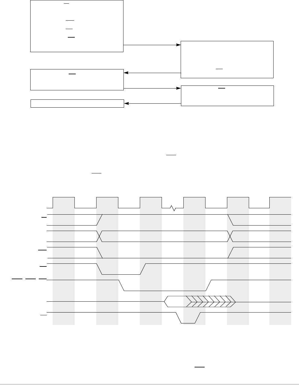
MOTOROLA Chapter 13. External Interface Module (EIM) 13-7
Data Transfer Operation
Figure 13-5. Read Cycle Flowchart
The read cycle timing diagram is shown in Figure 13-6.
NOTE:
In the following timing diagrams, TA waveforms apply for
chip selects programmed to enable either internal or external
termination. TA assertion should look the same in either case.
Figure 13-6. Basic Read Bus Cycle
Note the following characteristics of a basic read:
• In S3, data is made available by the external device on the falling edge of CLKOUT
and is sampled on the rising edge of CLKOUT with TA asserted.
System
1. Set R/W to read
2. Place address on A[31:0]
3. Assert TIP, and SIZ[1:0]
4. Assert TS
5. Negate TS
1. Decode address and select the
appropriate slave device.
2. Drive data on D[31:0]
3. Assert TA
1. Sample TA low and latch data
1. Negate TA.
2. Stop driving D[31:0]
1. Start next cycle
MCF5282
R/W
TIP
TS
D[31:0]
TA
Read
S0 S1 S2 S3 S4 S5
CLKOUT
CSn, BSn, OE
A[31:0], SIZ[1:0]
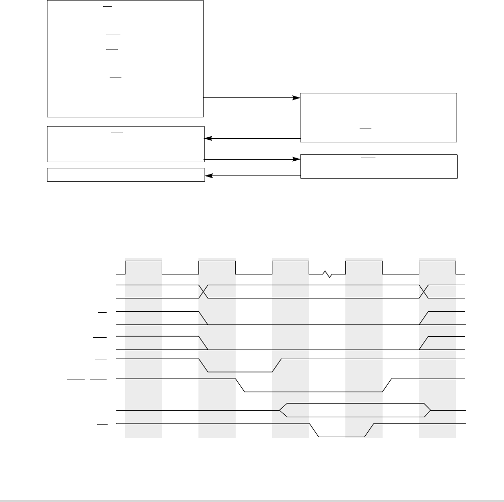
13-8 MCF5282 User’s Manual MOTOROLA
Data Transfer Operation
• In S4, the external device can stop driving data after the rising edge of CLKOUT.
However data could be driven up to S5.
• For a read cycle, the external device stops driving data between S4 and S5.
States are described in Table 13-3.
13.4.4 Write Cycle
During a write cycle, the MCF5282 sends data to the memory or to a peripheral device. The
write cycle flowchart is shown in Figure 13-7.
Figure 13-7. Write Cycle Flowchart
The write cycle timing diagram is shown in Figure 13-8.
Figure 13-8. Basic Write Bus Cycle
Table 13-3 describes the six states of a basic write cycle.
System
1. Set R/W to write
2. Place address on A[31:0]
3. Assert TIP and SIZ[1:0]
4. Assert TS
5. Place data on D[31:0]
6. Negate TS
1. Decode address
2. Store data on D[31:0]
3. Assert TA
1. Sample TA low
2. Stop driving data from D[31:0]
1. Negate TA
1. Start next cycle
MCF5282
R/W
TIP
TS
D[31:0]
TA
S0 S1 S2 S3 S4 S5
Write
CLKOUT
CSn, BSn
A[31:0], SIZ[1:0]
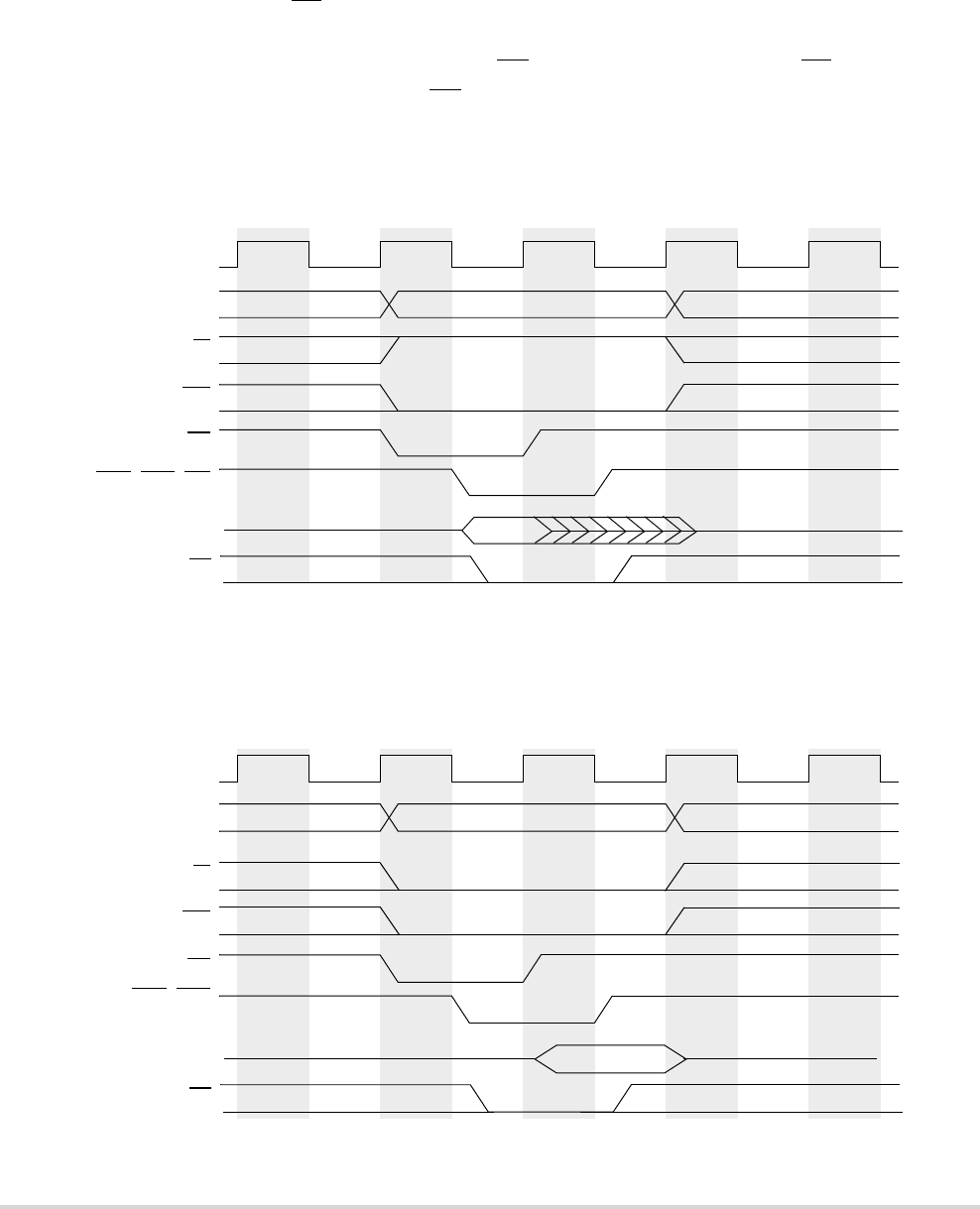
MOTOROLA Chapter 13. External Interface Module (EIM) 13-9
Data Transfer Operation
13.4.5 Fast Termination Cycles
Two clock cycle transfers are supported on the MCF5282 bus. In most cases, this is
impractical to use in a system because the termination must take place in the same
half-clock during which TS is asserted. As this is atypical, it is not referred to as the
zero-wait-state case but is called the fast-termination case. Fast termination cycles occur
when the external device or memory asserts TA less than one clock after TS is asserted.
This means that the MCF5282 samples TA on the rising edge of the second cycle of the bus
transfer. Figure 13-9 shows a read cycle with fast termination. Note that fast termination
cannot be used with internal termination.
Figure 13-9. Read Cycle with Fast Termination
Figure 13-10 shows a write cycle with fast termination.
Figure 13-10. Write Cycle with Fast Termination
R/W
TIP
TS
D[31:0]
TA
S0 S1 S4 S5
Read
CLKOUT
CSn, BSn, OE
A[31:0], SIZ[1:0]
R/W
TIP
TS
CSn, BSn
D[31:0]
TA
S0 S1 S4 S5
Write
CLKOUT
A[31:0], SIZ[1:0]
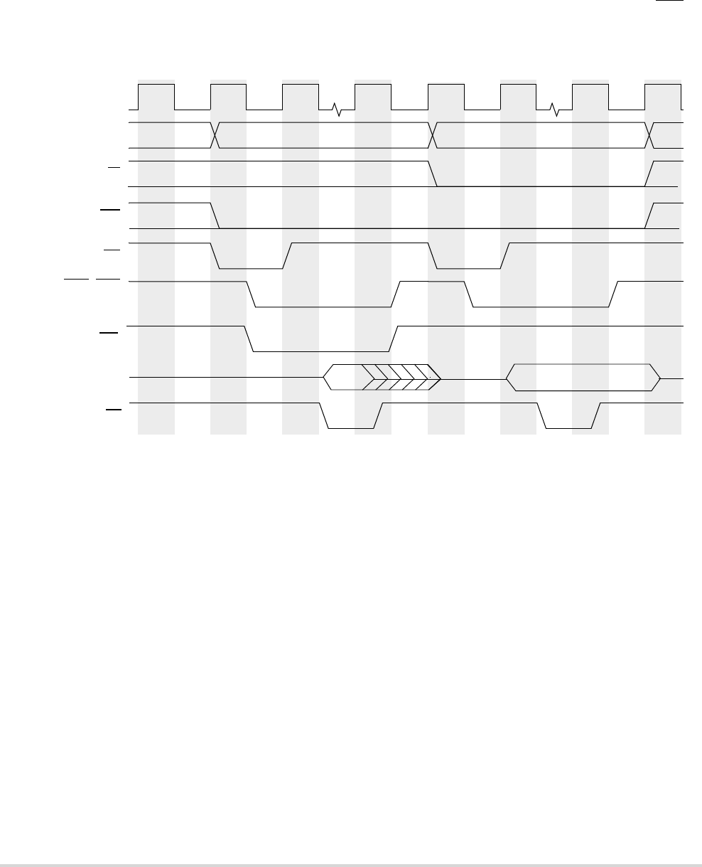
13-10 MCF5282 User’s Manual MOTOROLA
Data Transfer Operation
13.4.6 Back-to-Back Bus Cycles
The MCF5282 runs back-to-back bus cycles whenever possible. For example, when a
longword read is started on a word-size bus, the processor performs two back-to-back word
read accesses. Back-to-back accesses are distinguished by the continuous assertion of TIP
throughout the cycle. Figure 13-11 shows a read back-to-back with a write.
Figure 13-11. Back-to-Back Bus Cycles
Basic read and write cycles are used to show a back-to-back cycle, but there is no restriction
as to the type of operations to be placed back to back. The initiation of a back-to-back cycle
is not user definable.
13.4.7 Burst Cycles
The MCF5282 can be programmed to initiate burst cycles if its transfer size exceeds the
size of the port it is transferring to. For example, a word transfer to an 8-bit port would take
a 2-byte burst cycle. A line transfer to a 32-bit port would take a 4-longword burst cycle.
The MCF5282 bus can support 2-1-1-1 burst cycles to maximize cache performance and
optimize DMA transfers. A user can add wait states by delaying termination of the cycle.
The initiation of a burst cycle is encoded on the size pins. For burst transfers to smaller port
sizes, SIZ[1:0] indicates the size of the entire transfer. For example, if the MCF5282 writes
a longword to an 8-bit port, SIZ[1:0] = 00 for the first byte transfer and does not change.
The CSCRs can be used to enable bursting for reads, writes, or both. MCF5282 memory
space can be declared burst-inhibited for reads and writes by clearing the appropriate
R/W
TIP
TS
CSn, BSn
D[31:0]
TA
Read
S0 S1 S2 S3 S4 S5 S0 S1 S2 S3 S4 S5
Write
OE
CLKOUT
A[31:0], SIZ[1:0]
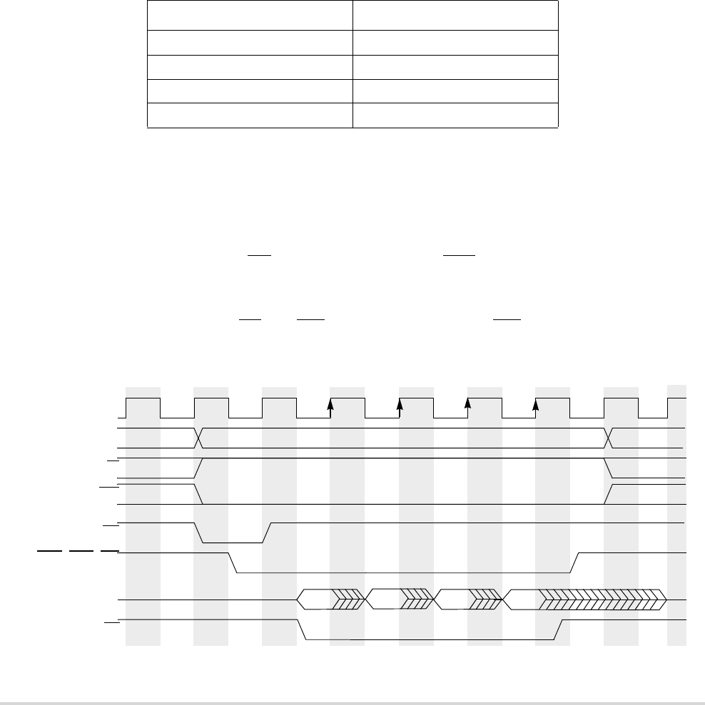
MOTOROLA Chapter 13. External Interface Module (EIM) 13-11
Data Transfer Operation
CSCRn[BSTR,BSTW]. A line access to a burst-inhibited region first accesses the
MCF5282 bus encoded as a line access. The SIZ[1:0] encoding does not exceed the
programmed port size. The address changes if internal termination is used but does not
change if external termination is used, as shown in Figure 13-12 and Figure 13-13.
13.4.7.1 Line Transfers
A line is a 16-byte-aligned, 16-byte value. Despite the alignment, a line access may not
begin on the aligned address; therefore, the bus interface supports line transfers on multiple
address boundaries. Table 13-4 shows allowable patterns for line accesses.
13.4.7.2 Line Read Bus Cycles
Figure 13-12 and Figure 13-13 show a line access read with zero wait states. The access
starts like a basic read bus cycle with the first data transfer sampled on the rising edge of
S4, but the next pipelined burst data is sampled a cycle later on the rising edge of S6. Each
subsequent pipelined data burst is single cycle until the last one, which can be held for up
to two CLKOUT cycles after TA is asserted. Note that CSn are asserted throughout the
burst transfer. This example shows the timing for external termination, which differs from
the internal termination example in Figure 13-13 only in that the address lines change only
at the beginning (assertion of TS and TIP) and end (negation of TIP) of the transfer.
Figure 13-12. Line Read Burst (2-1-1-1), External Termination
Table 13-4. Allowable Line Access Patterns
A[3:2] Longword Accesses
00 0–4–8–C
01 4–8–C–0
10 8–C–0–4
11 C–0–4–8
R/W
TIP
TS
CSn, BSn, OE
D[31:0]
TA
Read Read
S0 S1 S2 S3 S4 S5 S10S9S8S7S6 S11 S12 S13
Read Read
CLKOUT
A[31:0], SIZ[1:0]
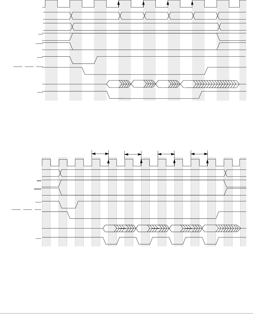
13-12 MCF5282 User’s Manual MOTOROLA
Data Transfer Operation
Figure 13-13 shows timing when internal termination is used.
Figure 13-13. Line Read Burst (2-1-1-1), Internal Termination
Figure 13-14 shows a line access read with one wait state programmed in CSCRn to give
the peripheral or memory more time to return read data. This figure follows the same
execution as a zero-wait state read burst with the exception of an added wait state.
.
Figure 13-14. Line Read Burst (3-2-2-2), External Termination
Figure 13-15 shows a burst-inhibited line read access with fast termination. The external
device executes a basic read cycle while determining that a line is being transferred. The
external device uses fast termination for subsequent transfers.
R/W
TIP
TS
CSn, BSn, OE
D[31:0]
TA
Read Read
S0 S1 S2 S3 S4 S5 S10S9S8S7S6 S11 S12 S13
Read Read
CLKOUT
A[31:0]
A[31:0], SIZ[1:0]
R/W
TIP
TS
CSn, BSn, OE
D[31:0]
TA
Read
S0 S1 S2 S3 S4 S5 S10
S9S8
S7
S6 S11S12
S13
WS WS WS WS
Read Read Read
CLKOUT
A[31:0], SIZ[1:0]
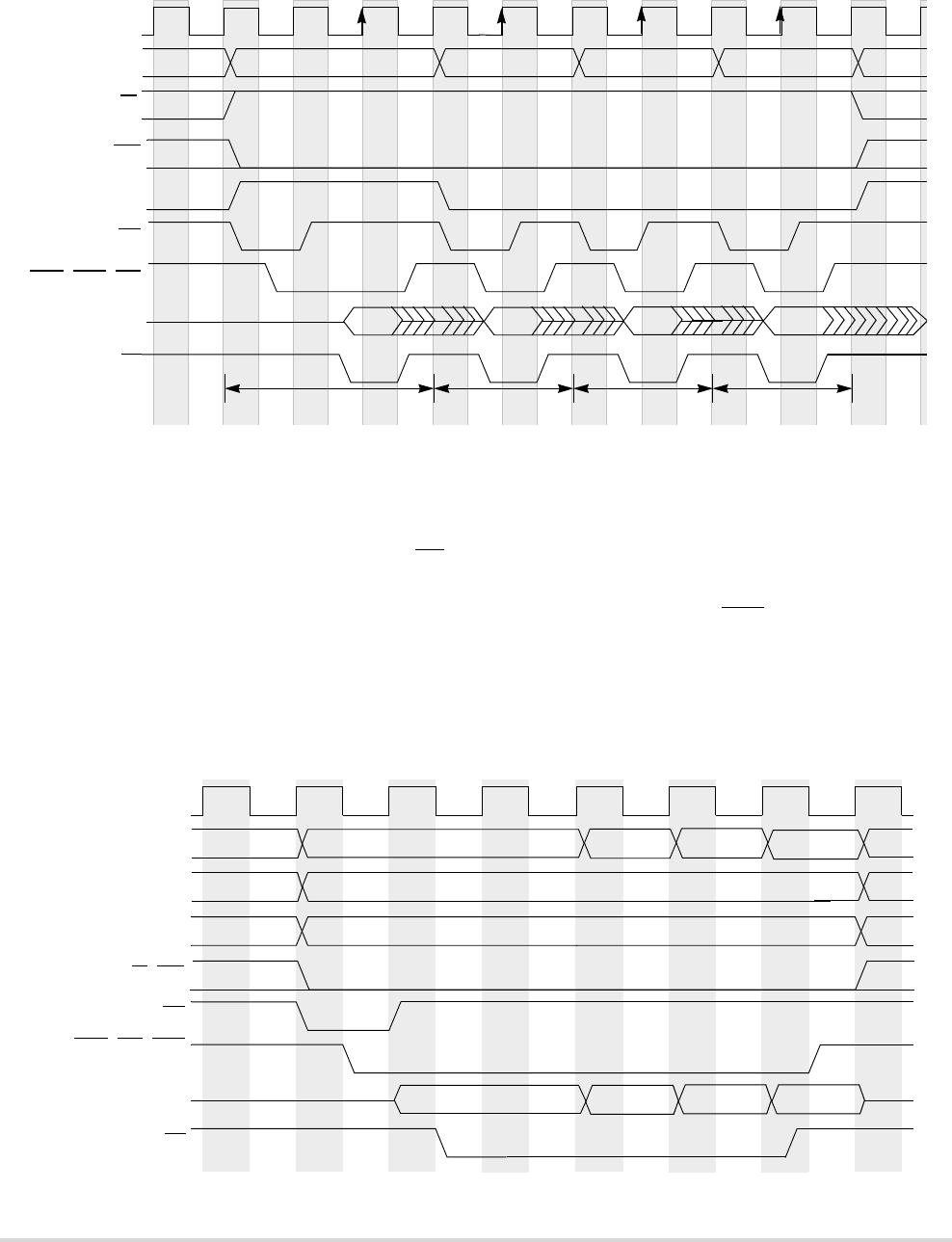
MOTOROLA Chapter 13. External Interface Module (EIM) 13-13
Data Transfer Operation
Figure 13-15. Line Read Burst-Inhibited, Fast Termination, External Termination
13.4.7.3 Line Write Bus Cycles
Figure 13-16 shows a line access write with zero wait states. It begins like a basic write bus
cycle with data driven one clock after TS. The next pipelined burst data is driven a cycle
after the write data is registered (on the rising edge of S6). Each subsequent burst takes a
single cycle. Note that as with the line read example in Figure 13-12, CSn remain asserted
throughout the burst transfer. This example shows the behavior of the address lines for both
internal and external termination. Note that when external termination is used, the address
lines change with SIZ[1:0].
Figure 13-16. Line Write Burst (2-1-1-1), Internal/External Termination
A[31:0]
R/W
TIP
SIZ[1:0]
TS
D[31:0]
TA
Line Longword
Basic Fast Fast Fast
A[3:2] = 00 A[3:2] = 01 A[3:2] = 10 A[3:2] = 11
S0 S1 S2 S3 S4 S5 S0 S1 S4 S5 S0 S1 S4 S5 S0 S1 S4 S5 S7S6
Read Read Read Read
CLKOUT
CSn, BSn, OE
A[31:0]
SIZ[1:0]
TS
CSn, OE, BSn
D[31:0]
TA
WriteWrite Write Write
S0 S1 S2 S3 S4 S5 S10S9S8S7S6 S11
CLKOUT
A[31:0]
Internal Termination
External Termination
R/W, TIP
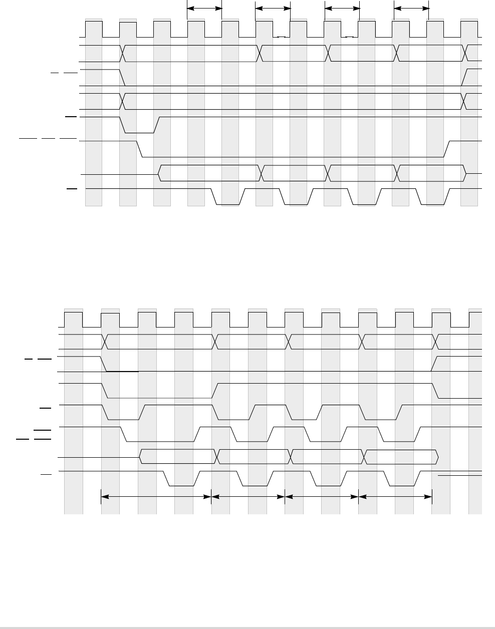
13-14 MCF5282 User’s Manual MOTOROLA
Misaligned Operands
Figure 13-17 shows a line burst write with one wait-state insertion.
Figure 13-17. Line Write Burst (3-2-2-2) with One Wait State
Figure 13-18 shows a burst-inhibited line write. The external device executes a basic write
cycle while determining that a line is being transferred. The external device uses fast
termination to end each subsequent transfer.
Figure 13-18. Line Write Burst-Inhibited
13.5 Misaligned Operands
Because operands can reside at any byte boundary, unlike opcodes, they are allowed to be
misaligned. A byte operand is properly aligned at any address, a word operand is
A[31:0]
R/W, TIP
TS
CSn, OE, BSn
D[31:0]
TA
Write Write Write Write
S0 S1 S2 S3 S4 S5 S10S9S8S7S6 S11
WS WS WS WS
CLKOUT
SIZ[1:0]
A[31:0]
R/W, TIP
SIZ[1:0]
TS
D[31:0]
TA
Line Longword
Basic Fast Fast Fast
A[3:2] = 00 A[3:2] = 01 A[3:2] = 10 A[3:2] = 11
Write Write Write Write
S0 S1 S2 S3 S4 S5 S0 S1 S4 S5 S0 S1 S4 S5 S0 S1 S4 S5
CLKOUT
CSn
OE, BSn

MOTOROLA Chapter 13. External Interface Module (EIM) 13-15
Misaligned Operands
misaligned at an odd address, and a longword is misaligned at an address not a multiple of
four. Although the MCF5282 enforces no alignment restrictions for data operands
(including program counter (PC) relative data addressing), additional bus cycles are
required for misaligned operands.
Instruction words and extension words (opcodes) must reside on word boundaries.
Attempting to prefetch a misaligned instruction word causes an address error exception.
The MCF5282 converts misaligned, cache-inhibited operand accesses to multiple aligned
accesses. Figure 13-19 shows the transfer of a longword operand from a byte address to a
32-bit port. In this example, SIZ[1:0] specify a byte transfer and a byte offset of 0x1. The
slave device supplies the byte and acknowledges the data transfer. When the MCF5282
starts the second cycle, SIZ[1:0] specify a word transfer with a byte offset of 0x2. The next
two bytes are transferred in this cycle. In the third cycle, byte 3 is transferred. The byte
offset is now 0x0, the port supplies the final byte, and the operation is complete.
Figure 13-19. Example of a Misaligned Longword Transfer (32-Bit Port)
If an operand is cacheable and is misaligned across a cache-line boundary, both lines are
loaded into the cache. The example in Figure 13-20 differs from that in Figure 13-19 in that
the operand is word-sized and the transfer takes only two bus cycles.
Figure 13-20. Example of a Misaligned Word Transfer (32-Bit Port)
Transfer 1
Transfer 2
Transfer 3
—
—
Byte 3
Byte 0
—
—
—
Byte 1
—
—
Byte 2
—
31 24 23 16 15 8 7 0
001
010
100
A[2
:
0]
Transfer 1
Transfer 2
—
Byte 1
—
—
—
—
Byte 0
—
31 24 23 16 15 8 7 0
001
100
A[2:0]

13-16 MCF5282 User’s Manual MOTOROLA
Misaligned Operands

MOTOROLA Chapter 14. Signal Descriptions 14-1
Chapter 14
Signal Descriptions
This chapter describes MCF5282 signals. It includes an alphabetical listing of signals that
characterizes each signal as an input or output, defines its state at reset, and identifies
whether a pull-up resistor should be used. Chapter 13, “External Interface Module (EIM),”
describes how these signals interact.
NOTE
The terms ‘assertion’ and ‘negation’ are used to avoid
confusion when dealing with a mixture of active-low and
active-high signals. The term ‘asserted’ indicates that a signal
is active, independent of the voltage level. The term ‘negated’
indicates that a signal is inactive.
Active-low signals, such as SRAS and TA, are indicated with
an overbar.
14.1 Overview
Figure 14-1 shows the block diagram of the MCF5282 with the signal interface.
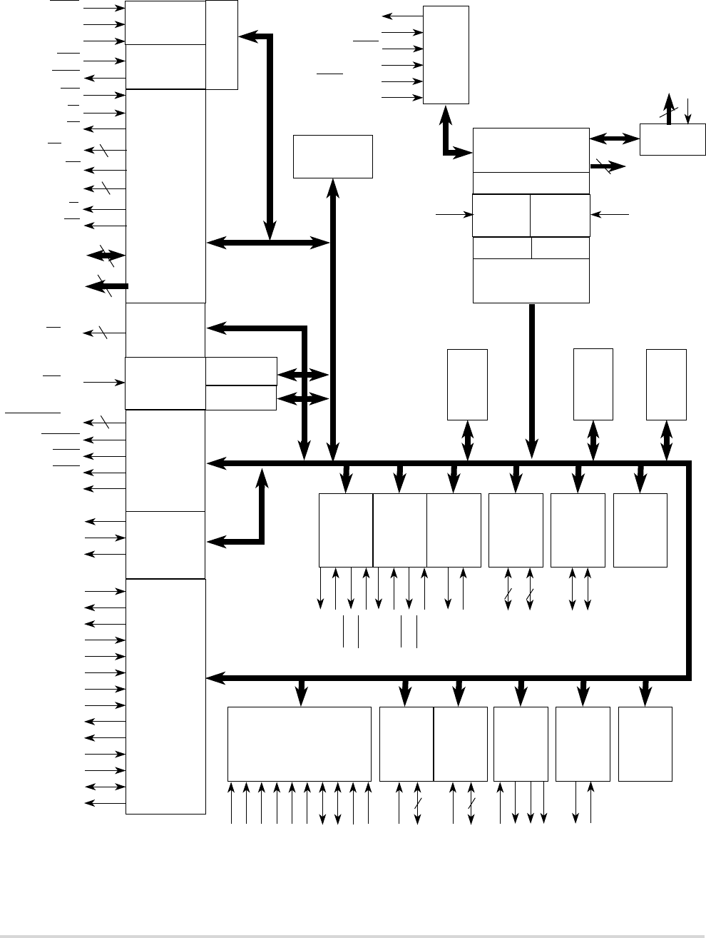
14-2 MCF5282 User’s Manual MOTOROLA
Overview
Figure 14-1. MCF5282 Block Diagram with Signal Interfaces
TDO/DSO
TDI/DSI
TMS/BKPT
TCLK
Interface
Chip
UART1
Serial
I/O
EXTAL
DTIN[3:0]
DTOUT[3:0]
TA
R/W
SIZ[1:0]
D[31:0]
A[23:0]
JTAG
Port
Selects
ColdFire V2 Core
EMAC
External
UTxD0
URxD0
URTS0
UCTS0
UTxD1
URxD1
URTS1
UCTS1
DRAMW
2
24
32
BS[3:0]
CS[6:0] 7
4
2
TEA
TRST/DSCLK
TEST
4
4
Tes t
Controller
OE
SRAS
SCAS
SCKE
TS
4
PST[3:0]
4
TIP
I2C
Module
SCL
SDA
UART2
Serial
I/O
DMA
Timer
Modules
DRAM
Controller
2-Kbyte
DDATA[3:0]
D-Cache/I-Cache
Debug Module
DIV
Clock Module
Chip
Configuration
Reset
Controller
Power
RCON
CLKMOD0
CLKMOD1
RSTI
RSTO
(PLL)
Edgeport
Interrupt
Controller 0
Interrupt
Controller 1
IRQ[7:1]
FEC
UART0
Serial
I/O
DMA
Controller
Watchdog
Timer
General
Purpose
Timer A
General
Purpose
Timer B
QSPI FlexCANQADC
PIT
Timers
(PIT0–
JTAG_EN
CLKOUT
XTAL
ETXCLK
ETXEN
ETXDO
ECOL
ERXCLK
ERXDV
ERXD0
ECRS
ETXD[3:1]
ETXER
ERXD[3:1]
ERXER
EMDIO
EMDC
UTxD2
URxD2
(DTIM0–
DTIM3)
VREFH
VREFL
AN0/ANW
AN1/ANX
AN2/ANY
AN3/ANZ
AN52/MA0
AN53/MA1
AN55/TRIG1
AN56/TRIG2
SYNCA
GPTA[3:0] 4
GPTB[3:0] 4
SYNCB
QSPI_DIN
QSPI_DOUT
QSPI_CLK
QSPI_CS[3:0]
CANTX
CANRX
Management
Module
Ports
Module
SDRAM_CS[1:0]
PIT3)
Internal Bus
Arbiter
System
Control
Module (SCM)
VDDF VSTBY
Flash
Module
64K
SRAM

MOTOROLA Chapter 14. Signal Descriptions 14-3
Overview
Table 14-1 lists the MCF5282 signals grouped by functionality.
NOTE:
The primary functionality of a pin is not necessarily its default
functionality. Pins that are muxed with GPIO will default to
their GPIO functionality.
Table 14-1. MCF5282 Signal Description
Signal Name Abbreviation Function I/O Page
External Memory Interface
Address A[23:0] Define the address of external byte,
word, longword, and 16-byte burst
accesses.
I/O 14-18
Data D[31:0] Data bus. Provide the general
purpose data path between the MCU
and all other devices.
I/O 14-18
Byte strobes BS[3:0] Define the byte lane of data on the
data bus.
I/O 14-19
Output enable OE Indicates when an external device can
drive data on the bus.
O 14-19
Transfer acknowledge TA Indicates that the external data
transfer is complete and should be
asserted for one clock.
I 14-19
Transfer error
acknowledge
TEA Indicates that an error condition exists
for the bus transfer.
I 14-19
Read/Write R/W Indicates the direction of the data
transfer on the bus.
I/O 14-19
Transfer size SIZ[1:0] Specify the data access size of the
current external bus reference.
O 14-19
Transfer start TS Asserted during the first CLKOUT
cycle of a transfer when address and
attributes are valid.
O 14-20
Transfer in progress TIP Asserted to indicate that a bus
transfer is in progress. Negated during
idle bus cycles.
O 14-20
Chip selects CS[6:0] Programmed for a base address
location and for masking addresses,
port size and burst capability
indication, wait state generation, and
internal/external termination.
O 14-20
SDRAM Controller Signals
SDRAM row
address strobe
SRAS SDRAM synchronous row address
strobe.
O 14-21
SDRAM column
address strobe
SCAS SDRAM synchronous column address
strobe.
O 14-21

14-4 MCF5282 User’s Manual MOTOROLA
Overview
SDRAM write enable DRAMW Asserted to signify that a DRAM write
cycle is underway. Negated to indicate
a read cycle.
O 14-21
SDRAM bank selects SDRAM_CS[1:0] Interface to the chip-select lines of the
SDRAMs within a memory block.
O 14-21
SDRAM clock enable SCKE SDRAM clock enable. O 14-21
Clock and Reset Signals
Reset in RSTI Asserted to enter reset exception
processing.
I 14-22
Reset out RSTO Automatically asserted with RSTI.
Negation indicates that the PLL has
regained its lock.
O 14-22
EXTAL EXTAL Driven by an external clock except
when used as a connection to the
external crystal.
I 14-22
XTAL XTAL Internal oscillator connection to the
external crystal.
O 14-22
Clock output CLKOUT Reflects the system clock. O 14-22
Chip Configuration Module
Clock mode CLKMOD[1:0] Clock mode select I 14-22
Reset configuration RCON Reset configuration select I 14-22
External Interrupt Signals
External interrupts IRQ[7:1] External interrupt sources. I 14-23
Ethernet Module Signals
Management data EMDIO Transfers control information between
the external PHY and the media
access controller.
I/O 14-23
Management data clock EMDC Provides a timing reference to the
PHY for data transfers on the EMDIO
signal.
O 14-23
Transmit clock ETXCLK Provides a timing reference for
ETXEN, ETXD[3:0], and ETXER.
I 14-23
Transmit enable ETXEN Indicates when valid nibbles are
present on the MII.
O 14-23
Transmit data 0 ETXD0 Serial output Ethernet data. O 14-23
Collision ECOL Asserted to indicate a collision. I 14-24
Receive clock ERXCLK Provides a timing reference for
ERXDV, ERXD[3:0], and ERXER.
I 14-24
Table 14-1. MCF5282 Signal Description (Continued)
Signal Name Abbreviation Function I/O Page

MOTOROLA Chapter 14. Signal Descriptions 14-5
Overview
Receive data valid ERXDV Asserted to indicate that the PHY has
valid nibbles present on the MII.
I 14-24
Receive data 0 ERXD0 Ethernet input data transferred from
the PHY to the media access
controller (when ERXDV is asserted).
I 14-24
Carrier receive sense ECRS Asserted to indicate that the transmit
or receive medium is not idle.
I 14-24
Transmit data ETXD[3:1] Contain the serial output Ethernet
data.
O 14-24
Transmit error ETXER Asserted (for one or more E_TXCLKs
while ETXEN is also asserted) to
cause the PHY to send one or more
illegal symbols.
O 14-24
Receive data ERXD[3:1] Contain the Ethernet input data
transferred from the PHY to the media
access controller (when ERXDV is
asserted in MII mode).
I 14-25
Receive error ERXER Indicates (when asserted with
ERXDV) that the PHY has detected
an error in the current frame.
I 14-25
Queued Serial Peripheral Interface (QSPI) Signals
QSPI synchronous
serial data output
QSPI_DOUT Provides serial data from the QSPI. O 14-25
QSPI synchronous
serial data input
QSPI_DIN Provides serial data to the QSPI. I 14-25
QSPI serial clock QSPI_CLK Provides the serial clock from the
QSPI.
O 14-25
QSPI chip selects QSPI_CS[3:0] Provide QSPI peripheral chip selects. O 14-25
FlexCAN Signals
FlexCAN transmit CANTX Controller area network transmit data. O 14-26
FlexCAN transmit CANRX Controller area network transmit data. I 14-26
I2C Signals
Serial clock SCL Clock signal for the I2C interface. I/O 14-26
Serial data SDA Data input/output for the I2C interface. I/O 14-26
UART Signals
Transmit serial
data output
UTXD[2:0] Transmitter serial data outputs. O 14-26
Receive serial
data input
URXD[2:0] Receiver serial data inputs. I 14-27
Table 14-1. MCF5282 Signal Description (Continued)
Signal Name Abbreviation Function I/O Page

14-6 MCF5282 User’s Manual MOTOROLA
Overview
Clear-to-send UCTS[1:0] Signals UART that it can begin data
transmission.
I 14-27
Request to send URTS[1:0] Automatic UART request to send
outputs.
O 14-27
General Purpose Timer Signals
GPTA GPTA[3:0] Provide the external interface to the
timer A functions.
I/O 14-27
GPTB GPTB[3:0] Provide the external interface to the
timer B functions.
I/O 14-27
External clock input SYNCA/SYNCB Clear the timer’s clock, providing a
means of synchronization to externally
clocked or timed events.
I 14-27
DMA Timer Signals
DMA timer input DTIN[3:0] Clock the event counter or provide a
trigger to timer value capture logic.
I/O 14-28
DMA timer output DTOUT[3:0] Pulse or toggle on timer events. I/O 14-28
Analog-to-Digital Converter (QADC) Signals
QADC analog input AN[0:3]/AN[W:Z] Direct analog input ANn, or
multiplexed input ANx.
I 14-29
QADC analog input AN[52:53]/MA[0:1] Direct analog input ANn, or
multiplexed output MAn. MAn selects
the output of the external multiplexer.
I/O 14-29
QADC analog input AN[55:56]/
TRIG[1:2]
Direct analog input ANn, or input
TRIGn. TRIGn causes one of the two
queues to execute.
I 14-30
Debug Support Signals
JTAG_EN JTAG_EN Selects between multiplexed debug
module and JTAG signals at reset.
I 14-30
Development serial
clock/Test reset
DSCLK/TRST Development serial clock for the serial
interface to debug module (DSCLK).
Asynchronously resets the internal
JTAG controller to the test logic reset
state (TRST).
I 14-30
Breakpoint/
Test mode select
BKPT/TMS Signals a hardware breakpoint in
debug mode (BKPT). Provides
information that determines JTAG test
operation mode (TMS).
I 14-31
Development serial
input/Test data
DSI/TDI Provides single-bit communication for
debug module commands (DSI).
Provides serial data port for loading
JTAG boundary scan, bypass, and
instruction registers (TDI).
I 14-31
Table 14-1. MCF5282 Signal Description (Continued)
Signal Name Abbreviation Function I/O Page

MOTOROLA Chapter 14. Signal Descriptions 14-7
Overview
Table 14-2 lists signals in alphabetical order by abbreviated name.
Development serial
output/Test data
DSO/TDO Provides single-bit communication for
debug module responses (DSO).
Provides serial data port for outputting
JTAG logic data (TDO).
O 14-31
Test clock TCLK JTAG test logic clock. I 14-31
Debug data DDATA[3:0] Display captured processor
addresses, data, and breakpoint
status.
O 14-32
Processor status
outputs
PST[3:0] Indicate core status. O 14-32
Test Signals
Test TEST Reserved, should be connected to
VSS.
I 14-32
Power and Reference Signals
QADC analog reference VRH, VRL High (VRH) and low (VRL) reference
potentials for the analog converter.
Ground 14-33
QADC analog supply VDDA, VSSA Isolate the QADC analog circuitry
from digital power supply noise.
I 14-33
PLL analog supply VDDPLL, VSSPLL Isolate the PLL analog circuitry from
digital power supply noise.
I 14-33
QADC positive supply VDDH Supplies positive power to the ESD
structures in the QADC pads.
I 14-33
Flash erase/program
power
VPP Used for Flash stress testing. I 14-33
Flash array power
and ground
VDDF, VSSF Supply power and ground to Flash
array.
I 14-33
Standby power VSTBY Provides standby voltage to RAM
array if VDD is lost.
I 14-33
Positive supply VDD Supplies positive power to the core
logic and I/O pads.
I 14-33
Ground VSS Negative supply. 14-33
Table 14-1. MCF5282 Signal Description (Continued)
Signal Name Abbreviation Function I/O Page

14-8 MCF5282 User’s Manual MOTOROLA
Overview
Table 14-2. MCF5282 Alphabetical Signal Index
Abbreviation Function I/O
A[23:0] Define the address of external byte, word, longword, and
16-byte burst accesses.
I/O
AN[0:3]/AN[W:Z] Direct analog input ANn, or multiplexed input ANx.I
AN[52:53]/MA[0:1] Direct analog input ANn, or multiplexed output MAn. MAn
selects the output of the external multiplexer.
I/O
AN[55:56]/
TRIG[1:2]
Direct analog input ANn, or input TRIGn. TRIGn causes one of
the two queues to execute.
I
Breakpoint/
Test mode select
Signals a hardware breakpoint in debug mode (BKPT).
Provides information that determines JTAG test operation
mode (TMS).
I
BS[3:0] Define the byte lane of data on the data bus. I/O
CANRX Controller area network transmit data. I
CANTX Controller area network transmit data. O
CLKMOD[1:0] Clock mode select I
CLKOUT Reflects the system clock. O
CS[6:0] Programmed for a base address location and for masking
addresses, port size and burst capability indication, wait state
generation, and internal/external termination.
O
D[31:0] Data bus. Provide the general purpose data path between the
MCU and all other devices.
I/O
DDATA[3:0] Display captured processor addresses, data, and breakpoint
status.
O
DSO/TDO Provides single-bit communication for debug module
responses (DSO). Provides serial data port for outputting JTAG
logic data (TDO).
O
DSI/TDI Development serial clock for the serial interface to debug
module (DSCLK). Asynchronously resets the internal JTAG
controller to the test logic reset state (TRST).
I
DSCLK/TRST Provides single-bit communication for debug module
commands (DSI). Provides serial data port for loading JTAG
boundary scan, bypass, and instruction registers (TDI).
I
DRAMW Asserted to signify that a DRAM write cycle is underway.
Negated to indicate a read cycle.
O
DTIN[3:0] Clock the event counter or provide a trigger to timer value
capture logic.
I/O
DTOUT[3:0] Pulse or toggle on timer events. I/O
ECOL Asserted to indicate a collision. I
ECRS Asserted to indicate that the transmit or receive medium is not
idle.
I
EMDC Provides a timing reference to the PHY for data transfers on
the EMDIO signal.
O

MOTOROLA Chapter 14. Signal Descriptions 14-9
Overview
EMDIO Transfers control information between the external PHY and
the media access controller.
I/O
ERXCLK Provides a timing reference for ERXDV, ERXD[3:0], and
ERXER.
I
ERXD[3:1] Contain the Ethernet input data transferred from the PHY to the
media access controller (when ERXDV is asserted in MII
mode).
I
ERXD0 Ethernet input data transferred from the PHY to the media
access controller (when ERXDV is asserted).
I
ERXDV Asserted to indicate that the PHY has valid nibbles present on
the MII.
I
ERXER Indicates (when asserted with ERXDV) that the PHY has
detected an error in the current frame.
I
ETXCLK Provides a timing reference for ETXEN, ETXD[3:0], and
ETXER.
I
ETXD[3:1] Contain the serial output Ethernet data. O
ETXD0 Serial output Ethernet data. O
ETXEN Indicates when valid nibbles are present on the MII. O
ETXER Asserted (for one or more E_TXCLKs while ETXEN is also
asserted) to cause the PHY to send one or more illegal
symbols.
O
EXTAL Driven by an external clock except when used as a connection
to the external crystal.
I
VDDF, VSSF Supply power and ground to Flash array. I
VPP Used for Flash stress testing. I
GPTA[3:0] Provide the external interface to the timer A functions. I/O
GPTB[3:0] Provide the external interface to the timer B functions. I/O
Ground Negative supply.
IRQ[7:1] External interrupt sources. I
JTAG_EN Selects between multiplexed debug module and JTAG signals
at reset.
I
OE Indicates when an external device can drive data on the bus. O
VDDPLL Isolate the PLL analog circuitry from digital power supply noise. I
VDD Supplies positive power to the core logic and I/O pads. I
PST[3:0] Indicate core status. O
VRH, VRL High (VRH) and low (VRL) reference potentials for the analog
converter.
I
VDDA, VSSA Isolate the QADC analog circuitry from digital power supply
noise.
I
Table 14-2. MCF5282 Alphabetical Signal Index (Continued)
Abbreviation Function I/O

14-10 MCF5282 User’s Manual MOTOROLA
Overview
QADC analog supply Supplies positive power to the ESD structures in the QADC
pads.
I
QSPI_CLK Provides the serial clock from the QSPI. O
QSPI_CS[3:0] Provide QSPI peripheral chip selects. O
QSPI_DIN Provides serial data to the QSPI. I
QSPI_DOUT Provides serial data from the QSPI. O
R/W Indicates the direction of the data transfer on the bus. I/O
RCON Reset configuration select. I
RSTI Asserted to enter reset exception processing. I
RSTO Automatically asserted with RSTI. Negation indicates that the
PLL has regained its lock.
O
SCAS SDRAM synchronous column address strobe. O
SCKE SDRAM clock enable. O
SCL Clock signal for the I2C interface. I/O
SDA Data input/output for the I2C interface. I/O
SDRAM_CS[1:0] Interface to the chip-select lines of the SDRAMs within a
memory block.
O
SIZ[1:0] Specify the data access size of the current external bus
reference.
O
SRAS SDRAM synchronous row address strobe. O
VSTBY Provides standby voltage to RAM array if VDD is lost. I
SYNCA/SYNCB Clear the timer’s clock, providing a means of synchronization
to externally clocked or timed events.
I
TA Indicates that the external data transfer is complete and should
be asserted for one CLKOUT cycle.
I
TEA Indicates that an error condition exists for the bus transfer. I
TEST Reserved, should be connected to VSS. I
TCK JTAG test logic clock. I
TIP Asserted to indicate that a bus transfer is in progress. Negated
during idle bus cycles.
O
TS Asserted during the first CLKOUT cycle of a transfer when
address and attributes are valid.
O
UCTS[1:0] Signals UART that it can begin data transmission. I
URTS[1:0] Automatic UART request to send outputs. O
URXD[2:0] Receiver serial data inputs. I
Table 14-2. MCF5282 Alphabetical Signal Index (Continued)
Abbreviation Function I/O
MOTOROLA Chapter 14. Signal Descriptions 14-11
Overview
UTXD[2:0] Transmitter serial data outputs. O
XTAL Internal oscillator connection to the external crystal. O
Table 14-3. MCF5282 Signals and Pin Numbers Sorted by Function
MAPBGA Pin
Pin Functions
Description Primary
I/O
Internal
Pull-up1
Primary2Secondary Tertiary
Reset
R11 RSTI — — Reset in IYes
P11 RSTO — — Reset out O —
Clock
T8 EXTAL — — External clock/crystal in I —
R8 XTAL — — Crystal drive O —
N7 CLKOUT — — Clock out O —
Chip Configuration/Mode Selection
R14 CLKMOD0 — — Clock mode select IYes
T14 CLKMOD1 — — Clock mode select IYes
T11 RCON — — Reset configuration enable IYes
H1 D26 PA2 —Chip mode I/O —
K2 D17 PB1 —Chip mode I/O —
K3 D16 PB0 —Chip mode I/O —
J4 D19 PB3 —Boot device/data port size I/O —
K1 D18 PB2 —Boot device/data port size I/O —
J2 D21 PB5 —Output pad drive strength I/O —
External Memory Interface and Ports
C6:B6:A5 A[23:21] PF[7:5] CS[6:4] Address bus O Yes
C4:B4:A4:B3:A3 A[20:16] PF[4:0] — Address bus O Yes
A2:B1:B2:C1:
C2:C3:D1:D2
A[15:8] PG[7:0] — Address bus O Yes
D3:D4:E1:E2:
E3:E4:F1:F2
A[7:0] PH[7:0] — Address bus O Yes
F3:G1:G2:G3:
G4:H1:H2:H3
D[31:24] PA[7:0] —Data bus I/O —
H4:J1:J2:J3:
J4:K1:K2:K3
D[23:16] PB[7:0] —Data bus I/O —
Table 14-2. MCF5282 Alphabetical Signal Index (Continued)
Abbreviation Function I/O
14-12 MCF5282 User’s Manual MOTOROLA
Overview
L1:L2:L3:L4:
M1:M2:M3:M4
D[15:8] PC[7:0] —Data bus I/O —
N1:N2:N3:P1:
N5:T6:R6:P6
D[7:0] PD[7:0] —Data bus I/O —
P14:T15:R15:R16 BS[3:0] PJ[7:4] — Byte strobe I/O Yes
N16 OE PE7 — Output enable I/O —
P16 TA PE6 —Transfer acknowledge I/O Yes
P15 TEA PE5 — Transfer error acknowledge I/O Yes
N15 R/W PE4 — Read/write I/O Yes
N14 SIZ1 PE3 SYNCA Transfer size I/O Yes3
M16 SIZ0 PE2 SYNCB Transfer size I/O Yes4
M15 TS PE1 SYNCA Transfer start I/O Yes
M14 TIP PE0 SYNCB Transfer in progress I/O Yes
Chip Selects
L16:L15:L14:L13 CS[3:0] PJ[3:0] — Chip selects 3-0 I/O Yes
C6:B6:A5 A[23:21] PF[7:5] CS[6:4] Chip selects 6-4 O Yes
SDRAM Controller
H15 SRAS PSD5 — SDRAM row address strobe I/O —
H16 SCAS PSD4 — SDRAM column
address strobe
I/O —
G15 DRAMW PSD3 — SDRAM write enable I/O —
H13:G16 SDRAM_CS[1:0] PSD[2:1] — SDRAM chip selects I/O —
H14 SCKE PSD0 — SDRAM clock enable I/O —
External Interrupts Port
B15:B16:C14:C15:
C16: D14:D15
IRQ[7:1] PNQ[7:1] —External interrupt request I/O —
Ethernet
C10 EMDIO PAS5 URXD2 Management channel
serial data
I/O —
B10 EMDC PAS4 UTXD2 Management channel clock I/O —
A8 ETXCLK PEH7 —MAC Transmit clock I/O —
D6 ETXEN PEH6 —MAC Transmit enable I/O —
D7 ETXD0 PEH5 —MAC Transmit data I/O —
Table 14-3. MCF5282 Signals and Pin Numbers Sorted by Function (Continued)
MAPBGA Pin
Pin Functions
Description Primary
I/O
Internal
Pull-up1
Primary2Secondary Tertiary

MOTOROLA Chapter 14. Signal Descriptions 14-13
Overview
B11 ECOL PEH4 —MAC Collision I/O —
A10 ERXCLK PEH3 —MAC Receive clock I/O —
C8 ERXDV PEH2 —MAC Receive enable I/O —
D9 ERXD0 PEH1 —MAC Receive data I/O —
A11 ECRS PEH0 —MAC Carrier sense I/O —
A7:B7:C7 ETXD[3:1] PEL[7:5] —MAC Transmit data I/O —
D10 ETXER PEL4 —MAC Transmit error I/O —
A9:B9:C9 ERXD[3:1] PEL[3:1] —MAC Receive data I/O —
B8 ERXER PEL0 —MAC Receive error I/O —
FlexCAN
D16 CANRX PAS3 URXD2 FlexCAN Receive data I/O —
E13 CANTX PAS2 UTXD2 FlexCAN Transmit data I/O —
I2C
E14 SDA PAS1 URXD2 I2C Serial data I/O Yes 5
E15 SCL PAS0 UTXD2 I2C Serial clock I/O Yes6
QSPI
F13 QSPI_DOUT PQS0 —QSPI data out I/O —
E16 QSPI_DIN PQS1 —QSPI data in I/O —
F14 QSPI_CLK PQS2 —QSPI clock I/O —
G14:G13:F16:F15 QSPI_CS[3:0] PQS[6:3] —QSPI chip select I/O —
Table 14-3. MCF5282 Signals and Pin Numbers Sorted by Function (Continued)
MAPBGA Pin
Pin Functions
Description Primary
I/O
Internal
Pull-up1
Primary2Secondary Tertiary
14-14 MCF5282 User’s Manual MOTOROLA
Overview
UARTs
R7 URXD1 PUA3 —U1 receive data I/O —
P7 UTXD1 PUA2 —U1 transmit data I/O —
N6 URXD0 PUA1 —U0 receive data I/O —
T7 UTXD0 PUA0 —U0 transmit data I/O —
C10 EMDIO PAS5 URXD2 U2 receive data I/O —
B10 EMDC PAS4 UTXD2 U2 transmit data I/O —
D16 CANRX PAS3 URXD2 U2 receive data I/O —
E13 CANTX PAS2 UTXD2 U2 transmit data I/O —
E14 SDA PAS1 URXD2 U2 receive data I/O Yes5
E15 SCL PAS0 UTXD2 U2 transmit data I/O Yes6
K16 DTIN3 PTC3 URTS1/
URTS0
U1/U0 Request to Send I/O —
K15 DTOUT3 PTC2 URTS1/
URTS0
U1/U0 Request to Send I/O —
K14 DTIN2 PTC1 UCTS1/
UCTS0
U1/U0 Clear to Send I/O —
K13 DTOUT2 PTC0 UCTS1/
UCTS0
U1/U0 Clear to Send I/O —
J16 DTIN1 PTD3 URTS1/
URTS0
U1/U0 Request to Send I/O —
J15 DTOUT1 PTD2 URTS1/
URTS0
U1/U0 Request to Send I/O —
J14 DTIN0 PTD1 UCTS1/
UCTS0
U1/U0 Clear to Send I/O —
J13 DTOUT0 PTD0 UCTS1/
UCTS0
U1/U0 Clear to Send I/O —
General Purpose Timers
T13:R13:P13:N13 GPTA[3:0] PTA[3:0] —Timer A IC/OC/PAI I/O Yes
T12:R12:P12:N12 GPTB[3:0] PTB[3:0] —Timer B IC/OC/PAI I/O Yes
N14 SIZ1 PE3 SYNCA Timer A synchronization input I/O Yes3
M16 SIZ0 PE2 SYNCB Timer B synchronization input I/O Yes4
M15 TS PE1 SYNCA Timer A synchronization input I/O Yes
M14 TIP PE0 SYNCB Timer B synchronization input I/O Yes
Table 14-3. MCF5282 Signals and Pin Numbers Sorted by Function (Continued)
MAPBGA Pin
Pin Functions
Description Primary
I/O
Internal
Pull-up1
Primary2Secondary Tertiary
MOTOROLA Chapter 14. Signal Descriptions 14-15
Overview
DMA Timers
K16 DTIN3 PTC3 URTS1/
URTS0
Timer 3 in I/O —
K15 DTOUT3 PTC2 URTS1/
URTS0
Timer 3 out I/O —
K14 DTIN2 PTC1 UCTS1/
UCTS0
Timer 2 in I/O —
K13 DTOUT2 PTC0 UCTS1/
UCTS0
Timer 2 out I/O —
J16 DTIN1 PTD3 URTS1/
URTS0
Timer 1 in I/O —
J15 DTOUT1 PTD2 URTS1/
URTS0
Timer 1 out I/O —
J14 DTIN0 PTD1 UCTS1/
UCTS0
Timer 0 in I/O —
J13 DTOUT0 PTD0 UCTS1/
UCTS0
Timer 0 out I/O —
Queued Analog-to-Digital Converter (QADC)
T3 AN0 PQB0 ANW Analog channel 0 I/O —
R2 AN1 PQB1 ANX Analog channel 1 I/O —
T2 AN2 PQB2 ANY Analog channel 2 I/O —
R1 AN3 PQB3 ANZ Analog channel 3 I/O —
R4 AN52 PQA0 MA0 Analog channel 52 I/O —
T4 AN53 PQA1 MA1 Analog channel 53 I/O —
P3 AN55 PQA3 ETRIG1 Analog channel 55 I/O —
R3 AN56 PQA4 ETRIG2 Analog channel 56 I/O —
P4 VRH — — High analog reference I —
T5 VRL — — Low analog reference I —
Debug and JTAG Test Port Control
R9 JTAG_EN — — JTAG Enable I —
P9 DSCLK TRST —Debug clock / TAP reset IYes7
T9 TCLK — — TAP clock IYes7
P10 BKPT TMS —Breakpoint/TAP test mode
select
IYes7
R10 DSI TDI —Debug data in / TAP data in IYes7
Table 14-3. MCF5282 Signals and Pin Numbers Sorted by Function (Continued)
MAPBGA Pin
Pin Functions
Description Primary
I/O
Internal
Pull-up1
Primary2Secondary Tertiary

14-16 MCF5282 User’s Manual MOTOROLA
Overview
14.1.1 Single-Chip Mode
In single-chip mode, signals default to GPIO inputs after a system reset. Table 14-4 is a
T10 DSO TDO —Debug data out / TAP data out O —
C12:D12:A13:B13 DDATA[3:0] PDD[7:4] —Debug data I/O —
C13:A14:B14:A15 PST[3:0] PDD[3:0] —Processor status data I/O —
Test
N10 TEST —Test mode pin I —
Power Supplies
R5 VDDA — — Analog positive supply I —
P5:T1 VSSA — — Analog ground I —
P2 VDDH — — ESD positive supply I —
N8 VDDPLL — — PLL positive supply I —
P8 VSSPLL — — PLL ground I —
A6:C11 VPP — — Flash (stress) programming
voltage
I —
A12:C5:D5:D11 VDDF — — Flash positive supply I —
B5:B12: VSSF — — Flash module ground I —
N11 VSTBY — — Standby power I —
E6-E11:F5:F7-F10:
F12:G5:G6:G11:
G12:H5:H6:H11:
H12:J5:J6:J11:J12:
K5:K6:K11:K12:L5:
L7-L10:L12:
M6-M11
VDD — — Positive supply I —
A1:A16:E5:E12:F6:
F11:G7-G10:H7-H10
:J7-J10:K7-K10:L6:
L11:M5:M12:T16
VSS — — Ground I —
1Pull-ups are not active when GPIO functions are selected for the pins.
2The primary functionality of a pin is not necessarily its default functionality. Pins that have GPIO functionality will
default to GPIO inputs.
3Pull-up is active only with the SYNCA function.
4Pull-up is active only with the SYNCB function.
5Pull-up is active only with the SDA function.
6Pull-up is active only with SCL function.
7Pull-up is active when JTAG_EN is driven high.
Table 14-3. MCF5282 Signals and Pin Numbers Sorted by Function (Continued)
MAPBGA Pin
Pin Functions
Description Primary
I/O
Internal
Pull-up1
Primary2Secondary Tertiary
MOTOROLA Chapter 14. Signal Descriptions 14-17
Overview
listing of signals that do not default to a GPIO function.
14.1.2 External Boot Mode
When booting from external memory, the address bus, data bus, and bus control signals will
default to their bus functionalities as shown in Table 14-5. As in single-chip mode, the
signals listed in Table 14-4 will operate as described above. All other signals will default to
GPIO inputs.
Table 14-4. Pin Reset States at Reset (Single-Chip Mode)
Signal Reset I/O
Clock and Reset Signals
RSTI —I
RSTO Low O
EXTAL —I
XTAL XTAL O
CLKOUT CLKOUT O
Debug Support Signals
JTAG_EN —I
DSCLK/TRST —I
BKPT/TMS —I
DSI/TDI —I
DSO/TDO High O
TCLK —I
DDATA[3:0] DDATA{3:0] O
PST[3:0] PST[3:0] O
Table 14-5. Default Signal Functions After System
Reset (External Boot Mode)
Signal Reset I/O
A[23:0] A[23:0] O
D[31:0] — I/O
BS[3:0] High O
OE High O
TA —I
TEA —I
R/W High O
SIZ[1:0] High O

14-18 MCF5282 User’s Manual MOTOROLA
MCF5282 External Signals
14.2 MCF5282 External Signals
The bus signals provide the external bus interface to the MCF5282.
14.2.1 External Interface Module (EIM) Signals
These signals are used for doing transactions on the external bus.
14.2.1.1 Address Bus (A[23:0])
The 24 dedicated address signals, A[23:0], define the address of external byte, word,
longword and 16-byte burst accesses. These three-state outputs are the 24 lsbs of the
internal 32-bit address bus. The address lines also serve as the SDRAM addressing,
providing multiplexed row and column address signals.
These pins are configured for GPIO ports F, G and H in single-chip mode. The A[23:21]
pins can also be configured for CS[6:4].
14.2.1.2 Data Bus (D[31:0])
These three-state bidirectional signals provide the general purpose data path between the
MCU and all other devices. Data is sampled by the MCF5282 on the rising CLKOUT edge.
The data bus port width and wait states are initially defined for the external boot chip select,
CS0, by D[19:18] during chip configuration at reset. The port width for each chip select and
SDRAM bank is programmable. The data bus uses a default configuration if none of the
chip selects or SDRAM bank match the address decode. The default configuration is a
32-bit port with external termination and burst-inhibited transfers. The data bus can transfer
byte, word, or longword data widths. All 32 data bus signals are driven during writes,
regardless of port width and operand size.
D[26:24, 21, 19:16] are used during chip configuration as inputs to configure the functions
as described in Chapter 30, “Chip Configuration Module (CCM).”
These pins are configured as GPIO ports A, B, C and D in single-chip mode.
14.2.1.3 Byte Strobes (BS[3:0])
The byte strobes (BS[3:0]) define the byte lane of data on the data bus. During accesses,
TS High O
TIP High O
CS[6:0] High O
Table 14-5. Default Signal Functions After System
Reset (External Boot Mode) (Continued)
Signal Reset I/O

MOTOROLA Chapter 14. Signal Descriptions 14-19
MCF5282 External Signals
these outputs act as the byte select signals that indicate valid data is to be latched or driven
onto a byte lane when driven low. For SRAM or Flash devices, the BS[3:0] outputs should
be connected to individual byte strobe signals. For SDRAM devices, the BS[3:0] should be
connected to individual SDRAM DQM signals. Note that most SDRAMs associate DQM3
with the MSB, in which case BS3 is connected to the SDRAM's DQM3 input.
These pins can also be configured as GPIO PJ[7:4].
14.2.1.4 Output Enable (OE)
This output signal indicates when an external device can drive data during external read
cycles.
This pin can also be configured as GPIO PE7.
14.2.1.5 Transfer Acknowledge (TA)
This signal indicates that the external data transfer is complete. During a read cycle, when
the processor recognizes TA, it latches the data and then terminates the bus cycle. During a
write cycle, when the processor recognizes TA, the bus cycle is terminated. If all bus cycles
support fast termination, TA can be tied low.
This pin can also be configured as GPIO PE6.
14.2.1.6 Transfer Error Acknowledge (TEA)
This signal indicates an error condition exists for the bus transfer. The bus cycle is
terminated and the CPU begins execution of the access error exception. This signal is an
input in master mode.
This pin can also be configured as GPIO PE5.
14.2.1.7 Read/Write (R/W)
This output signal indicates the direction of the data transfer on the bus. A logic 1 indicates
a read from a slave device and a logic 0 indicates a write to a slave device.
This pin can also be configured as GPIO PE4.
14.2.1.8 Transfer Size(SIZ[1:0])
When the device is in normal mode, static bus sizing lets the programmer change data bus
width between 8, 16, and 32 bits for each chip select. The SIZ[1:0] outputs specify the data
access size of the current external bus reference as shown in Table 14-6.

14-20 MCF5282 User’s Manual MOTOROLA
MCF5282 External Signals
Note that for misaligned transfers, SIZ[1:0] indicate the size of each transfer. For example,
if a longword access occurs at a misaligned offset of 0x1, a byte is transferred first (SIZ[1:0]
= 01), a word is next transferred at offset 0x2 (SIZ[1:0] = 10), then the final byte is
transferred at offset 0x4 (SIZ[1:0] = 01).
For aligned transfers larger than the port size, SIZ[1:0] behaves as follows:
• If bursting is used, SIZ[1:0] stays at the size of transfer.
• If bursting is inhibited, SIZ[1:0] first shows the size of the transfer and then shows
the port size.
For burst-inhibited transfers, SIZ[1:0] changes with each TS assertion to reflect the next
transfer size. For transfers to port sizes smaller than the transfer size, SIZ[1:0] indicates the
size of the entire transfer on the first access and the size of the current port transfer on
subsequent transfers. For example, for a longword write to an 8-bit port, SIZ[1:0] = 00 for
the first byte transfer and 01 for the next three.
These pins can also be configured as GPIO PE[3:2] or SYNCA, SYNCB.
14.2.1.9 Transfer Start (TS)
The MCF5282 asserts TS during the first CLKOUT cycle of a transfer when address and
attributes (TIP, R/W, and SIZ[1:0]) are valid. TS is negated in the following CLKOUT
cycle.
This pin can also be configured as GPIO PE1 or SYNCA.
14.2.1.10 Transfer In Progress (TIP)
The TIP output is asserted indicating a bus transfer is in progress. It is negated during idle
bus cycles. Note that TIP is held asserted on back-to-back cycles.
NOTE:
TIP is not asserted during SDRAM accesses.
This pin can also be configured as GPIO PE0 or SYNCB.
14.2.1.11 Chip Selects (CS[6:0])
Each chip select can be programmed for a base address location and for masking addresses,
Table 14-6. Transfer Size Encoding
SIZ[1:0] Transfer Size
00 Longword
01 Byte
10 Word
11 16-byte line

MOTOROLA Chapter 14. Signal Descriptions 14-21
MCF5282 External Signals
port size and burst-capability indication, wait-state generation, and internal/external
termination.
Reset clears all chip select programming; CS0 is the only chip select initialized out of reset.
CS0 is also unique because it can function at reset as a global chip select that allows boot
ROM to be selected at any defined address space. The port size for boot CS0 is set during
chip configuration by the levels on D[19:18] on the rising edge of RSTI, as described in
Chapter 30, “Chip Configuration Module (CCM).” The chip-select implementation is
described in Chapter 12, “Chip Select Module.”
These pins can also be configured as A[23:21] and GPIO PJ[3:0].
14.2.2 SDRAM Controller Signals
These signals are used for SDRAM accesses.
14.2.2.1 SDRAM Row Address Strobe (SRAS)
This output is the SDRAM synchronous row address strobe.
This pin is configured as GPIO PSD5 in single-chip mode.
14.2.2.2 SDRAM Column Address Strobe (SCAS)
This output is the SDRAM synchronous column address strobe.
This pin is configured as GPIO PSD4 in single-chip mode.
14.2.2.3 SDRAM Write Enable (DRAMW)
The DRAM write signal (DRAMW) is asserted to signify that a DRAM write cycle is
underway. A read cycle is indicated by the negation of DRAMW.
This pin is configured as GPIO PSD3 in single-chip mode.
14.2.2.4 SDRAM Bank Selects (SDRAM_CS[1:0])
These signals interface to the chip-select lines of the SDRAMs within a memory block.
Thus, there is one SDRAM_CS line for each memory block (the MCF5282 supports two
SDRAM memory blocks).
These pins is configured as GPIO PSD[2:1] in single-chip mode.
14.2.2.5 SDRAM Clock Enable (SCKE)
This output is the SDRAM clock enable.
This pin is configured as GPIO PSD0 in single-chip mode.

14-22 MCF5282 User’s Manual MOTOROLA
MCF5282 External Signals
14.2.3 Clock and Reset Signals
The clock and reset signals configure the MCF5282 and provide interface signals to the
external system.
14.2.3.1 Reset In (RSTI)
Asserting RSTI causes the MCF5282 to enter reset exception processing. When RSTI is
recognized the address bus, data bus, SIZ, R/W, AS, and TS are three-stated. RSTO is
asserted automatically when RSTI is asserted.
14.2.3.2 Reset Out (RSTO)
After RSTI is asserted, the PLL temporarily loses its lock, during which time RSTO is
asserted. When the PLL regains its lock, RSTO negates again. This signal can be used to
reset external devices.
14.2.3.3 EXTAL
This input is driven by an external clock except when used as a connection to the external
crystal when using the internal oscillator.
14.2.3.4 XTAL
This output is an internal oscillator connection to the external crystal.
14.2.3.5 Clock Output (CLKOUT)
The internal PLL generates CLKOUT. This output reflects the internal system clock.
14.2.4 Chip Configuration Signals
14.2.4.1 RCON
If the external RCON signal is asserted, then various chip functions, including the reset
configuration pin functions after reset, are configured according to the levels driven onto
the external data pins (see Section 30.6, “Functional Description”). The internal
configuration signals are driven to reflect the levels on the external configuration pins to
allow for module configuration.
14.2.4.2 CLKMOD[1:0]
The state of the CLKMOD[1:0] pins during reset determines the clock mode after reset.

MOTOROLA Chapter 14. Signal Descriptions 14-23
MCF5282 External Signals
14.2.5 External Interrupt Signals
14.2.5.1 External Interrupts (IRQ[7:1])
These inputs are the external interrupt sources. See Chapter 11, “Edge Port Module
(EPORT)” for more information on these interrupt sources and their corresponding
registers.
These pins are configured as GPIO PNQ[7:1] in single-chip mode.
14.2.6 Ethernet Module Signals
The following signals are used by the Ethernet module for data and clock signals.
14.2.6.1 Management Data (EMDIO)
The bidirectional EMDIO signal transfers control information between the external PHY
and the media-access controller. Data is synchronous to EMDC and applies to MII mode
operation. This signal is an input after reset. When the FEC is operated in 10 Mbps 7-wire
interface mode, this signal should be connected to VSS.
This pin can also be configured as GPIO PAS5 or URXD2.
14.2.6.2 Management Data Clock (EMDC)
EMDC is an output clock which provides a timing reference to the PHY for data transfers
on the EMDIO signal and applies to MII mode operation.
This pin can also be configured as GPIO PAS4 or UTXD2.
14.2.6.3 Transmit Clock (ETXCLK)
This is an input clock which provides a timing reference for ETXEN, ETXD[3:0] and
ETXER.
This pin can also be configured as GPIO PEH7.
14.2.6.4 Transmit Enable (ETXEN)
The transmit enable (ETXEN) output indicates when valid nibbles are present on the MII.
This signal is asserted with the first nibble of a preamble and is negated before the first
ETXCLK following the final nibble of the frame.
This pin can also be configured as GPIO PEH6.
14.2.6.5 Transmit Data 0 (ETXD0)
ETXD0 is the serial output Ethernet data and is only valid during the assertion of ETXEN.
This signal is used for 10 Mbps Ethernet data. This signal is also used for MII mode data
in conjunction with ETXD[3:1].

14-24 MCF5282 User’s Manual MOTOROLA
MCF5282 External Signals
This pin can also be configured as GPIO PEH5.
14.2.6.6 Collision (ECOL)
The ECOL input is asserted upon detection of a collision and remains asserted while the
collision persists. This signal is not defined for full-duplex mode.
This pin can also be configured as GPIO PEH4.
14.2.6.7 Receive Clock (ERXCLK)
The receive clock (ERXCLK) input provides a timing reference for ERXDV, ERXD[3:0],
and ERXER.
This pin can also be configured as GPIO PEH3.
14.2.6.8 Receive Data Valid (ERXDV)
Asserting the receive data valid (ERXDV) input indicates that the PHY has valid nibbles
present on the MII. ERXDV should remain asserted from the first recovered nibble of the
frame through to the last nibble. Assertion of ERXDV must start no later than the SFD and
exclude any EOF.
This pin can also be configured as GPIO PEH2.
14.2.6.9 Receive Data 0 (ERXD0)
ERXD0 is the Ethernet input data transferred from the PHY to the media-access controller
when ErXDV is asserted. This signal is used for 10 Mbps Ethernet data. This signal is also
used for MII mode Ethernet data in conjunction with ERXD[3:1]. This pin can also be
configured as GPIO PEH1.
14.2.6.10 Carrier Receive Sense (ECRS)
ECRS is an input signal which, when asserted, signals that transmit or receive medium is
not idle, and applies to MII mode operation.
This pin can also be configured as GPIO PEH0.
14.2.6.11 Transmit Data 1-3 (ETXD[3:1])
These pins contain the serial output Ethernet data and are valid only during assertion of
ETXEN in MII mode.
These pins can also be configured as GPIO PEL[7:5].
14.2.6.12 Transmit Error (ETXER)
When the ETXER output is asserted for one or more E_TXCLKs while ETXEN is also
asserted, the PHY sends one or more illegal symbols. ETXER has no effect at 10 Mbps or
when ETXEN is negated, and applies to MII mode operation.

MOTOROLA Chapter 14. Signal Descriptions 14-25
MCF5282 External Signals
These pins can also be configured as GPIO PEL4.
14.2.6.13 Receive Data 1–3 (ERXD[3:1])
These pins contain the Ethernet input data transferred from the PHY to the media-access
controller when ERXDV is asserted in MII mode operation.
These pins can also be configured as GPIO PEL[3:1].
14.2.6.14 Receive Error (ERXER)
ERXER is an input signal which when asserted along with ERXDV signals that the PHY
has detected an error in the current frame. When ERXDV is not asserted ERXER has no
effect, and applies to MII mode operation.
These pins can also be configured as GPIO PEL0.
14.2.7 Queued Serial Peripheral Interface (QSPI) Signals
14.2.7.1 QSPI Synchronous Serial Output (QSPI_DOUT)
The QSPI_DOUT output provides the serial data from the QSPI and can be programmed to
be driven on the rising or falling edge of QSPICLK. Each byte is sent msb first.
This pin can also be configured as GPIO PQS0.
14.2.7.2 QSPI Synchronous Serial Data Input (QSPI_DIN)
The QSPI_DIN input provides the serial data to the QSPI and can be programmed to be
sampled on the rising or falling edge of QSPICLK. Each byte is written to RAM lsb first.
This pin can also be configured as GPIO PQS1.
14.2.7.3 QSPI Serial Clock (QSPI_CLK)
The QSPI serial clock (QSPI_CLK) provides the serial clock from the QSPI. The polarity
and phase of QSPI_CLK are programmable. The output frequency is programmed
according to the following formula, in which n can be any value between 2 and 255:
QSPI_CLK = CLKOUT/(2n).
This pin can also be configured as GPIO PQS2.
14.2.7.4 QSPI Chip Selects (QSPI_CS[3:0])
The synchronous peripheral chip selects (QSPI_CS[3:0]) outputs provide QSPI peripheral
chip selects that can be programmed to be active high or low.
This pin can also be configured as GPIO PQS[6:3].

14-26 MCF5282 User’s Manual MOTOROLA
MCF5282 External Signals
14.2.8 FlexCAN Signals
14.2.8.1 FlexCAN Transmit (CANTX)
Controller Area Network Transmit data output.
This pin can also be configured as GPIO PAS2.
14.2.8.2 FlexCAN Receive (CANRX)
Controller Area Network Transmit data input.
This pin can also be configured as GPIO PAS3.
14.2.9 I2C Signals
The I2C module acts as a two-wire, bidirectional serial interface between the MCF5282 and
peripherals with an I2C interface (such as LCD controller, A-to-D converter, or D-to-A
converter). Devices connected to the I2C must have open-drain or open-collector outputs.
14.2.9.1 Serial Clock (SCL)
This bidirectional open-drain signal is the clock signal for the I2C interface. Either it is
driven by the I2C module when the bus is in the master mode or it becomes the clock input
when the I2C is in the slave mode.
This pin can also be configured as GPIO PAS0 or UTXD2.
14.2.9.2 Serial Data (SDA)
This bidirectional open-drain signal is the data input/output for the I2C interface.
This pin can also be configured as GPIO PAS1 or URXD2.
14.2.10 UART Module Signals
The signals in the following sections are used to transfer serial data between three UART
modules and external peripherals.
14.2.10.1 Transmit Serial Data Output (UTXD[2:0])
UTXD[2:0] are the transmitter serial data outputs for the UART modules. The output is
held high (mark condition) when the transmitter is disabled, idle, or in the local loopback
mode. Data is shifted out, lsb first, on this pin at the falling edge of the serial clock source.
The UTXD[1:0] pins can be configured as GPIO ports PUA2 and PUA0. The UTXD2
output is offered on 3 pins and is a secondary function of the EMDC/ GPIO port PAS4 pin,
CANTX/GPIO port PAS2 pin, and SCL/GPIO port PAS0 pin.

MOTOROLA Chapter 14. Signal Descriptions 14-27
MCF5282 External Signals
14.2.10.2 Receive Serial Data Input (URXD[2:0])
URXD[2:0] are the receiver serial data inputs for the UART modules. Data received on
these pins is sampled on the rising edge of the serial clock source lsb first. When the UART
clock is stopped for power-down mode, any transition on this pin restarts it.
The URXD[1:0] pins can be configured as GPIO ports PUA3 and PUA1. The URXD2
input is offered on 3 pins and is a secondary function of the EMDIO/GPIO port PAS5 pin,
CANRX/GPIO port PAS3 pin, and SDA/GPIO port PAS1 pin.
14.2.10.3 Clear-to-Send (UCTS[1:0])
The UCTS[1:0] signals are the clear-to-send (CTS) inputs, indicating to the UART modules
that they can begin data transmission.
The UCTS[1:0] inputs are each offered as secondary functions on four pins--DTIN2,
DTOUT2, DTIN0 and DTOUT0.
14.2.10.4 Request-to-Send (URTS[1:0])
The URTS[1:0] signals are automatic request to send outputs from the UART modules.
URTS[1:0] can also be configured to be asserted and negated as a function of the Rx FIFO
level.
The URTS[1:0] outputs are each offered as secondary functions on four pins: DTIN3,
DTOUT3, DTIN1 and DTOUT1.
14.2.11 General Purpose Timer Signals
These pins provide the external interface to the general purpose timer functions.
14.2.11.1 GPTA[3:0]
These pins provide the external interface to the timer A functions.
These pins can also be configured as GPIO PTA[3:0].
14.2.11.2 GPTB[3:0]
These pins provide the external interface to the timer B functions.
These pins can also be configured as GPIO PTB[3:0].
14.2.11.3 External Clock Input (SYNCA/SYNCB)
These pins are used to clear the clock for each of the two timers, and are provided as a
means of synchronization to externally clocked or timed events.

14-28 MCF5282 User’s Manual MOTOROLA
MCF5282 External Signals
14.2.12 DMA Timer Signals
This section describes the signals of the four DMA timer modules.
14.2.12.1 DMA Timer 0 Input (DTIN0)
The DMA timer 0 input (DTIN0) can be programmed to cause events to occur in DMA
timer 0. It can either clock the event counter or provide a trigger to the timer value capture
logic.
This pin can also be configured as GPIO PTD1, secondary function UCTS1, or secondary
function UCTS0.
14.2.12.2 DMA Timer 0 Output (DTOUT0)
The programmable DMA timer output (DTOUT0) pulse or toggle on various timer events.
This pin can also be configured as GPIO PTD0, secondary function UCTS1, or secondary
function UCTS0.
14.2.12.3 DMA Timer 1 Input (DTIN1)
The DMA timer 1 input (DTIN1) can be programmed to cause events to occur in DMA
timer 1. This can either clock the event counter or provide a trigger to the timer value
capture logic.
This pin can also be configured as GPIO PTD3, secondary function URTS1, or secondary
function URTS0.
14.2.12.4 DMA Timer 1 Output (DTOUT1)
The programmable DMA timer output (DTOUT1) pulse or toggle on various timer events.
This pin can also be configured as GPIO PTD2, secondary function URTS1, or secondary
function URTS0.
14.2.12.5 DMA Timer 2 Input (DTIN2)
The DMA timer 2 input (DTIN2) can be programmed to cause events to occur in DMA
timer 2. It can either clock the event counter or provide a trigger to the timer value capture
logic.
This pin can also be configured as GPIO PTC1, secondary function UCTS1, or secondary
function UCTS0.
14.2.12.6 DMA Timer 2 Output (DTOUT2)
The programmable DMA timer output (DTOUT2) pulse or toggle on various timer events.
This pin can also be configured as GPIO PTC0, secondary function UCTS1, or secondary
function UCTS0.

MOTOROLA Chapter 14. Signal Descriptions 14-29
MCF5282 External Signals
14.2.12.7 DMA Timer 3 Input (DTIN3)
The DMA timer 3 input (DTIN3) can be programmed as an input that causes events to
occur in DMA timer 3. This can either clock the event counter or provide a trigger to the
timer value capture logic. This pin can also be configured as GPIO PTC3, secondary
function URTS1, or secondary function URTS0.
14.2.12.8 DMA Timer 3 Output (DTOUT3)
The programmable DMA timer output (DTOUT0) pulse or toggle on various timer events.
This pin can also be configured as GPIO PTC2, secondary function URTS1, or secondary
function URTS0.
14.2.13 Analog-to-Digital Converter Signals
These pins provide the analog inputs to the QADC.
The PQA and PQB pins may also be used as general purpose digital I/O.
14.2.13.1 QADC Analog Input (AN0/ANW)
This PQB signal is the direct analog input AN0. When using external multiplexing this pin
can also be configured as multiplexed input ANW.
This pin can also be configured as GPIO PQB0.
14.2.13.2 QADC Analog Input (AN1/ANX)
This PQB signal is the direct analog input AN1. When using external multiplexing this pin
can also be configured as multiplexed input ANX.
This pin can also be configured as GPIO PQB1.
14.2.13.3 QADC Analog Input (AN2/ANY)
This PQB signal is the direct analog input AN2. When using external multiplexing this pin
can also be configured as multiplexed input ANY.
This pin can also be configured as GPIO PQB2.
14.2.13.4 QADC Analog Input (AN3/ANZ)
This PQB signal is the direct analog input AN3. When using external multiplexing this pin
can also be configured as multiplexed input ANZ.
This pin can also be configured as GPIO PQB3.
14.2.13.5 QADC Analog Input (AN52/MA0)
This PQA signal is the direct analog input AN52. When using external multiplexing this

14-30 MCF5282 User’s Manual MOTOROLA
MCF5282 External Signals
pin can also be configured as an output signal, MA0, to select the output of the external
multiplexer.
This pin can also be configured as GPIO PQA0.
14.2.13.6 QADC Analog Input (AN53/MA1)
This PQA signal is the direct analog input AN53. When using external multiplexing this
pin can also be configured as an output signal, MA1, to select the output of the external
multiplexer.
This pin can also be configured as GPIO PQA1.
14.2.13.7 QADC Analog Input (AN55/TRIG1)
This PQA signal is the direct analog input AN55. This pin can also be configured as an
input signal, TRIG1, to trigger the execution of one of the two queues.
This pin can also be configured as GPIO PQA3.
14.2.13.8 QADC Analog Input (AN56/TRIG2)
This PQA signal is the direct analog input AN56. This pin can also be configured as an
input signal, TRIG2, to trigger the execution of one of the two queues.
This pin can also be configured as GPIO PQA4.
14.2.14 Debug Support Signals
These signals are used as the interface to the on-chip JTAG controller and also to interface
to the BDM logic.
14.2.14.1 JTAG_EN
This input signal is used to select between multiplexed debug module and JTAG signals at
reset. If JTAG_EN is low, the part is in normal and background debug mode (BDM); if it
is high, it is in normal and JTAG mode.
14.2.14.2 Development Serial Clock/Test Reset (DSCLK/TRST)
Debug mode operation: DSCLK is selected. DSCLK is the development serial clock for the
serial interface to the debug module. The maximum DSCLK frequency is 1/5 CLKIN.
JTAG mode operation: TRST is selected. TRST asynchronously resets the internal JTAG
controller to the test logic reset state, causing the JTAG instruction register to choose the
bypass instruction. When this occurs, JTAG logic is benign and does not interfere with
normal MCF5282 functionality.
Although TRST is asynchronous, Motorola recommends that it makes an

MOTOROLA Chapter 14. Signal Descriptions 14-31
MCF5282 External Signals
asserted-to-negated transition only while TMS is held high. TRST has an internal pull-up
resistor so if it is not driven low, it defaults to a logic level of 1. If TRST is not used, it can
be tied to ground or, if TCK is clocked, to VDD. Tying TRST to ground places the JTAG
controller in test logic reset state immediately. Tying it to VDD causes the JTAG controller
(if TMS is a logic level of 1) to eventually enter test logic reset state after 5 TCK clocks.
14.2.14.3 Breakpoint/Test Mode Select (BKPT/TMS)
Debug mode operation: If JTAG_EN is low, BKPT is selected. BKPT signals a hardware
breakpoint to the processor in debug mode.
JTAG mode operation: TMS is selected. The TMS input provides information to determine
the JTAG test operation mode. The state of TMS and the internal 16-state JTAG controller
state machine at the rising edge of TCK determine whether the JTAG controller holds its
current state or advances to the next state. This directly controls whether JTAG data or
instruction operations occur. TMS has an internal pull-up resistor so that if it is not driven
low, it defaults to a logic level of 1. But if TMS is not used, it should be tied to VDD.
14.2.14.4 Development Serial Input/Test Data (DSI/TDI)
Debug mode operation: If JTAG_EN is low, DSI is selected. DSI provides the single-bit
communication for debug module commands.
JTAG mode operation: TDI is selected. TDI provides the serial data port for loading the
various JTAG boundary scan, bypass, and instruction registers. Shifting in data depends on
the state of the JTAG controller state machine and the instruction in the instruction register.
Shifts occur on the TCK rising edge. TDI has an internal pull-up resistor, so when not
driven low it defaults to high. But if TDI is not used, it should be tied to VDD.
14.2.14.5 Development Serial Output/Test Data (DSO/TDO)
Debug mode operation: DSO is selected. DSO provides single-bit communication for
debug module responses.
JTAG mode operation: TDO is selected. The TDO output provides the serial data port for
outputting data from JTAG logic. Shifting out data depends on the JTAG controller state
machine and the instruction in the instruction register. Data shifting occurs on the falling
edge of TCK. When TDO is not outputting test data, it is three-stated. TDO can be
three-stated to allow bused or parallel connections to other devices having JTAG.
14.2.14.6 Test Clock (TCLK)
TCK is the dedicated JTAG test logic clock independent of the MCF5282 processor clock.
Various JTAG operations occur on the rising or falling edge of TCK. Holding TCK high or
low for an indefinite period does not cause JTAG test logic to lose state information. If TCK
is not used, it must be tied to ground.

14-32 MCF5282 User’s Manual MOTOROLA
MCF5282 External Signals
14.2.14.7 Debug Data (DDATA[3:0])
Debug data signals (DDATA[3:0]) display captured processor addresses, data and
breakpoint status.
These pins can also be configured as GPIO PDD[7:4].
14.2.14.8 Processor Status Outputs (PST[3:0])
PST[3:0] outputs indicate core status, as shown below in Table 14-7. Debug mode timing
is synchronous with the processor clock; status is unrelated to the current bus transfer.
These pins can also be configured as GPIO PDD[3:0].
14.2.15 Test Signals
14.2.15.1 Test (TEST)
This input signal is reserved for factory testing only and should be connected to VSS to
prevent unintentional activation of test functions.
Table 14-7. Processor Status Encoding
PST[3:0] Definition
0000 Continue execution
0001 Begin execution of an instruction
0010 Reserved
0011 Entry into user mode
0100 Begin execution of PULSE and WDDATA
instruction
0101 Begin execution of taken branch
0110 Reserved
0111 Begin execution of RTE instruction
1000 Begin one-byte transfer on DDATA
1001 Begin two-byte transfer on DDATA
1010 Begin three-byte transfer on DDATA
1011 Begin four-byte transfer on DDATA
1100 Exception Processing
1101 Emulator-Mode Exception Processing
1110 Processor is stopped
1111 Processor is halted

MOTOROLA Chapter 14. Signal Descriptions 14-33
MCF5282 External Signals
14.2.16 Power and Reference Signals
These signals provide system power, ground and references to the device. Multiple pins are
provided for adequate current capability. All power supply pins must have adequate bypass
capacitance for high-frequency noise suppression.
14.2.16.1 QADC Analog Reference (VRH, VRL)
These signals serve as the high (VRH) and low (VRL) reference potentials for the analog
converter in the QADC.
14.2.16.2 QADC Analog Supply (VDDA, VSSA)
These are dedicated power supply signals to isolate the sensitive QADC analog circuitry
from the normal levels of noise present on the digital power supply.
14.2.16.3 PLL Analog Supply (VDDPLL, VSSPLL)
These are dedicated power supply signals to isolate the sensitive PLL analog circuitry from
the normal levels of noise present on the digital power supply.
14.2.16.4 QADC Positive Supply (VDDH)
This pin supplies positive power to the ESD structures in the QADC pads.
14.2.16.5 Power for Flash Erase/Program (VPP)
This pin is used for Flash stress testing and can be left unconnected in normal device
operation.
14.2.16.6 Power and Ground for Flash Array (VDDF, VSSF)
These signals supply a power and ground to the Flash array.
14.2.16.7 Standby Power (VSTBY)
This pin is used to provide standby voltage to the RAM array if VDD is lost.
14.2.16.8 Positive Supply (VDD)
This pin supplies positive power to the core logic and I/O pads.
14.2.16.9 Ground (VSS)
This pin is the negative supply (ground) to the chip.

14-34 MCF5282 User’s Manual MOTOROLA
MCF5282 External Signals

MOTOROLA Chapter 15. Synchronous DRAM Controller Module 15-1
Chapter 15
Synchronous DRAM Controller Module
This chapter describes configuration and operation of the synchronous DRAM (SDRAM)
controller. It begins with a general description and brief glossary, and includes a description
of signals involved in DRAM operations. The remainder of the chapter describes the
programming model and signal timing, as well as the command set required for
synchronous operations. It also includes extensive examples that the designer can follow to
better understand how to configure the DRAM controller for synchronous operations.
15.1 Overview
The synchronous DRAM controller module provides glueless integration of SDRAM with
the ColdFire product. The key features of the DRAM controller include the following:
• Support for two independent blocks of SDRAM
• Interface to standard SDRAM components
• Programmable SRAS, SCAS, and refresh timing
• Support for 8-, 16-, and 32-bit wide SDRAM blocks
15.1.1 Definitions
The following terminology is used in this chapter:
• SDRAM block: Any group of DRAM memories selected by one of the MCF5282
SRAS[1:0] signals. Thus, the MCF5282 can support two independent memory
blocks. The base address of each block is programmed in the DRAM address and
control registers (DACR0 and DACR1).
• SDRAM: RAMs that operate like asynchronous DRAMs but with a synchronous
clock, a pipelined, multiple-bank architecture, and a faster speed.
• SDRAM bank: An internal partition in an SDRAM device. For example, a 64-Mbit
SDRAM component might be configured as four 512K x 32 banks. Banks are
selected through the SDRAM component’s bank select lines.
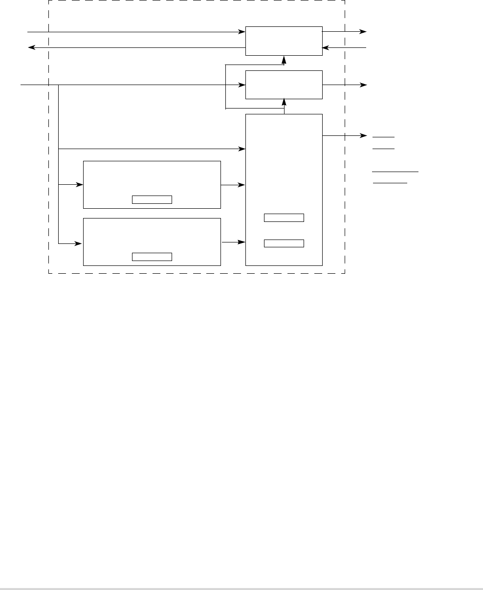
15-2 MCF5282 User’s Manual MOTOROLA
Overview
15.1.2 Block Diagram and Major Components
The basic components of the SDRAM controller are shown in Figure 15-1.
Figure 15-1. Synchronous DRAM Controller Block Diagram
The DRAM controller’s major components are as follows:
• DRAM address and control registers (DACR0 and DACR1)—The DRAM
controller consists of two configuration register units, one for each supported
memory block. DACR0 is accessed at IPSBAR + 0x048; DACR1 is accessed at
IPSBAR + 0x050. The register information is passed on to the hit logic.
• Control logic and state machine—Generates all SDRAM signals, taking hit
information and bus-cycle characteristic data from the block logic in order to
generate SDRAM accesses. Handles refresh requests from the refresh counter.
— DRAM control register (DCR)—Contains data to control refresh operation of the
DRAM controller. Both memory blocks are refreshed concurrently as controlled
by DCR[RC].
— Refresh counter—Determines when refresh should occur; controlled by the
value of DCR[RC]. It generates a refresh request to the control block.
• Hit logic—Compares address and attribute signals of a current SDRAM bus cycle
to both DACRs to determine if an SDRAM block is being accessed. Hits are passed
to the control logic along with characteristics of the bus cycle to be generated.
Memory Block 0 Hit Logic
DRAM Address/Control Register 0
(DACR0)
A[31:0]
Internal
Address
Control Logic
and
DRAMW
DRAM Controller Module
Refresh Counter
SCAS
SRAS
SCKE
State Machine
Multiplexing
DRAM Control
Register (DCR)
Bus
Memory Block 1 Hit Logic
DRAM Address/Control Register 1
(DACR1)
A[31:0]
SDRAM_CS[1:0]
BS[3:0]
Data
Generation
D[31:0] internal
Q[31:0] internal D[31:0]
D[31:0]

MOTOROLA Chapter 15. Synchronous DRAM Controller Module 15-3
SDRAM Controller Operation
• Address multiplexing—Multiplexes addresses to allow column and row addresses
to share pins. This allows glueless interface to SDRAMs.
• Data Generation—Controls the data input and data output transmission between the
on-platform and off-platform data buses.
15.2 SDRAM Controller Operation
By running synchronously with the system clock, SDRAM can (after an initial latency
period) be accessed on every clock; 5-1-1-1 is a typical MCF5282 burst rate to the
SDRAM. Unlike the MCF5272, the MCF5282 does not have an independent SDRAM
clock signal. For the MCF5282, the timing of the SDRAM controller is controlled by the
CLKOUT signal.
Note that because the MCF5282 cannot have more than one page open at a time, it does not
support interleaving.
SDRAM controllers are more sophisticated than asynchronous DRAM controllers. Not
only must they manage addresses and data, but they must send special commands for such
functions as precharge, read, write, burst, auto-refresh, and various combinations of these
functions. Table 15-1 lists common SDRAM commands.
SDRAMs operate differently than asynchronous DRAMs, particularly in the use of data
pipelines and commands to initiate special actions. Commands are issued to memory using
specific encodings on address and control pins. Soon after system reset, a command must
be sent to the SDRAM mode register to configure SDRAM operating parameters.
Table 15-1. SDRAM Commands
Command Definition
ACTV Activate. Executed before READ or WRITE executes; SDRAM registers and decodes row address.
MRS Mode register set.
NOP No-op. Does not affect SDRAM state machine; DRAM controller control signals negated; SRAS asserted.
PALL Precharge all. Precharges all internal banks of an SDRAM component; executed before new page is opened.
READ Read access. SDRAM registers column address and decodes that a read access is occurring.
REF Refresh. Refreshes internal bank rows of an SDRAM component.
SELF Self refresh. Refreshes internal bank rows of an SDRAM component when it is in low-power mode.
SELFX Exit self refresh. This command is sent to the DRAM controller when DCR[IS] is cleared.
WRITE Write access. SDRAM registers column address and decodes that a write access is occurring.
15-4 MCF5282 User’s Manual MOTOROLA
SDRAM Controller Operation
15.2.1 DRAM Controller Signals
Table 15-2 describes the behavior of DRAM signals in synchronous mode.
15.2.2 Memory Map for SDRAMC Registers
The DRAM controller registers memory map is shown in Table 15-3.
Table 15-2. Synchronous DRAM Signal Connections
Signal Description
SRAS Synchronous row address strobe. Indicates a valid SDRAM row address is present and can be latched by the SDRAM.
SRAS should be connected to the corresponding SDRAM SRAS.
SCAS Synchronous column address strobe. Indicates a valid column address is present and can be latched by the SDRAM.
SCAS should be connected to the corresponding SDRAM SCAS.
DRAMW DRAM read/write. Asserted for write operations and negated for read operations.
SDRAM_CS[1:0] Row address strobe. Select each memory block of SDRAMs connected to the MCF5282. One SDRAM_CS signal
selects one SDRAM block and connects to the corresponding CS signals.
SCKE Synchronous DRAM clock enable. Connected directly to the CKE (clock enable) signal of SDRAMs. Enables and
disables the clock internal to SDRAM. When CKE is low, memory can enter a power-down mode in which operations
are suspended or capable of entering self-refresh mode. SCKE functionality is controlled by DCR[COC]. For designs
using external multiplexing, setting COC allows SCKE to provide command-bit functionality.
BS[3:0] Column address strobe. BS[3:0] function as byte enables to the SDRAMs. They connect to the BS signals (or mask
qualifiers) of the SDRAMs.
Table 15-3. DRAM Controller Registers
IPSBAR
Offset [31:24] [23:16] [15:8] [7:0]
0x040 DRAM control register (DCR) [p. 15-5] —
0x044 —
0x048 DRAM address and control register 0 (DACR0) [p. 15-6]
0x04C DRAM mask register block 0 (DMR0) [p. 15-8]
0x050 DRAM address and control register 1 (DACR1) [p. 15-6]
0x054 DRAM mask register block 1 (DMR1) [p. 15-8]

MOTOROLA Chapter 15. Synchronous DRAM Controller Module 15-5
SDRAM Controller Operation
15.2.2.1 DRAM Control Register (DCR)
The DCR, shown in Figure 15-2, controls refresh logic.
Table 15-4 describes DCR fields.
15 14 13 12 11 10 9 8 0
Field — NAM COC IS RTIM RC
Reset Uninitialized
R/W R/W
Addr IPSBAR + 0x040
Figure 15-2. DRAM Control Register (DCR)
Table 15-4. DCR Field Descriptions
Bits Name Description
15-14 — Reserved, should be cleared.
13 NAM No address multiplexing. Some implementations require external multiplexing. For example, when linear
addressing is required, the SDRAM should not multiplex addresses on SDRAM accesses.
0 The SDRAM controller multiplexes the external address bus to provide column addresses.
1 The SDRAM controller does not multiplex the external address bus to provide column addresses.
12 COC Command on SDRAM clock enable (SCKE). Implementations that use external multiplexing (NAM = 1) must
support command information to be multiplexed onto the SDRAM address bus.
0 SCKE functions as a clock enable; self-refresh is initiated by the SDRAM controller through DCR[IS].
1 SCKE drives command information. Because SCKE is not a clock enable, self-refresh cannot be used (setting
DCR[IS]). Thus, external logic must be used if this functionality is desired. External multiplexing is also
responsible for putting the command information on the proper address bit.
11 IS Initiate self-refresh command.
0 Take no action or issue a SELFX command to exit self refresh.
1 If DCR[COC] = 0, the SDRAM controller sends a SELF command to both SDRAM blocks to put them in
low-power, self-refresh state where they remain until IS is cleared. When IS is cleared, the controller sends a
SELFX command for the SDRAMs to exit self-refresh. The refresh counter is suspended while the SDRAMs
are in self-refresh; the SDRAM controls the refresh period.
10–9 RTIM Refresh timing. Determines the timing operation of auto-refresh in the SDRAM controller. Specifically, it
determines the number of bus clocks inserted between a REF command and the next possible ACTV command.
This same timing is used for both memory blocks controlled by the SDRAM controller. This corresponds to tRC
in the SDRAM specifications.
00 3 clocks
01 6 clocks
1x 9 clocks
8–0 RC Refresh count. Controls refresh frequency. The number of bus clocks between refresh cycles is (RC + 1) x 16.
Refresh can range from 16–8192 bus clocks to accommodate both standard and low-power SDRAMs with bus
clock operation from less than 2 MHz to greater than 50 MHz.
The following example calculates RC for an auto-refresh period for 4096 rows to receive 64 ms of refresh every
15.625 µs for each row (1031 bus clocks at 66 MHz). This operation is the same as in asynchronous mode.
# of bus clocks = 1031 = (RC field + 1) x 16
RC = (1031 bus clocks/16) -1 = 63.44, which rounds to 63; therefore, RC = 0x3F.

15-6 MCF5282 User’s Manual MOTOROLA
SDRAM Controller Operation
15.2.2.2 DRAM Address and Control Registers (DACR0/DACR1)
The DACRn registers, shown in Figure 15-3, contain the base address compare value and
the control bits for memory blocks 0 and 1 of the SDRAM controller. Address and timing
are also controlled by bits in DACRn.
Table 15-5 describes DACRn fields.
31 18 17 16 15 14 13 12 11 10 9 8 7 6 5 4 3 2 0
Field BA — RE — CASL — CBM — IMRS PS IP —
Reset Uninitialized 0 Uninitialized 0 Uninitialized
R/W R/W
Address IPSBAR+0x048 (DACR0); 0x050 (DACR1)
Figure 15-3. DRAM Address and Control Register (DACRn)
Table 15-5. DACRn Field Descriptions
Bit Name Description
31–18 BA Base address register. With DCMR[BAM], determines the address range in which the associated DRAM block is
located. Each BA bit is compared with the corresponding address of the current bus cycle. If all unmasked bits
match, the address hits in the associated DRAM block. BA functions the same as in asynchronous operation.
17–16 — Reserved, should be cleared.
15 RE Refresh enable. Determines when the DRAM controller generates a refresh cycle to the DRAM block.
0 Do not refresh associated DRAM block
1 Refresh associated DRAM block
14 — Reserved, should be cleared.
13–12 CASL CAS latency. Affects the following SDRAM timing specifications. Timing nomenclature varies with
manufacturers. Refer to the SDRAM specification for the appropriate timing nomenclature:
Parameter
Number of Bus Clocks
CASL= 00 CASL = 01 CASL= 10 CASL= 11
tRCD—SRAS assertion to SCAS assertion 1 2 3 3
tCASL—SCAS assertion to data out 1 2 3 3
tRAS—ACTV command to precharge command 2 4 6 6
tRP—Precharge command to ACTV command 1 2 3 3
tRWL,tRDL—Last data input to precharge command 1 1 1 1
tEP—Last data out to precharge command 1 1 1 1
11 — Reserved, should be cleared.
MOTOROLA Chapter 15. Synchronous DRAM Controller Module 15-7
SDRAM Controller Operation
10–8 CBM Command and bank MUX [2:0]. Because different SDRAM configurations cause the command and bank select
lines to correspond to different addresses, these resources are programmable. CBM determines the addresses onto
which these functions are multiplexed.
This encoding and the address multiplexing scheme handle common SDRAM organizations. Bank select bits
include a base bit and all address bits above for SDRAMs with multiple bank select bits.
7 — Reserved, should be cleared.
6 IMRS Initiate mode register set (MRS) command. Setting IMRS generates a MRS command to the associated SDRAMs.
In initialization, IMRS should be set only after all DRAM controller registers are initialized and PALL and
REFRESH commands have been issued. After IMRS is set, the next access to an SDRAM block programs the
SDRAM’s mode register. Thus, the address of the access should be programmed to place the correct mode
information on the SDRAM address pins. Because the SDRAM does not register this information, it doesn’t
matter if the IMRS access is a read or a write or what, if any, data is put onto the data bus. The DRAM controller
clears IMRS after the MRS command finishes.
0 Take no action
1 Initiate MRS command
5–4 PS Port size. Indicates the port size of the associated block of SDRAM, which allows for dynamic sizing of
associated SDRAM accesses. PS functions the same in asynchronous operation.
00 32-bit port
01 8-bit port
1x 16-bit port
3 IP Initiate precharge all (PALL) command. The DRAM controller clears IP after the PALL command is finished.
Accesses via IP should be no wider than the port size programmed in PS.
0 Take no action.
1A
PALL command is sent to the associated SDRAM block. During initialization, this command is executed
after all DRAM controller registers are programmed. After IP is set, the next write to an appropriate SDRAM
address generates the PALL command to the SDRAM block.
2–0 — Reserved, should be cleared.
Table 15-5. DACRn Field Descriptions (continued)
Bit Name Description
CBM Command Bit Bank Select Bits
000 17 18 and up
001 18 19 and up
010 19 20 and up
011 20 21 and up
100 21 22 and up
101 22 23 and up
110 23 24 and up
111 24 25 and up

15-8 MCF5282 User’s Manual MOTOROLA
SDRAM Controller Operation
15.2.2.3 DRAM Controller Mask Registers (DMR0/DMR1)
The DMRn, Figure 15-4, includes mask bits for the base address and for address attributes.
Table 15-6 describes DMRn fields.
31 1817 9876543210
Field BAM — WP — C/I AM SC SD UC UD V
Reset Uninitialized 0
R/W R/W
Addr IPSBAR + 0x04C (DMR0), 0x054 (DMR1)
Figure 15-4. DRAM Controller Mask Registers (DMRn)
Table 15-6. DMRn Field Descriptions
Bits Name Description
31–18 BAM Base address mask. Masks the associated DACRn[BA]. Lets the DRAM controller connect to various DRAM
sizes. Mask bits need not be contiguous (see Section 15.3, “SDRAM Example.”)
0 The associated address bit is used in decoding the DRAM hit to a memory block.
1 The associated address bit is not used in the DRAM hit decode.
17–9 — Reserved, should be cleared.
8 WP Write protect. Determines whether the associated block of DRAM is write protected.
0 Allow write accesses
1 Ignore write accesses. The DRAM controller ignores write accesses to the memory block and an address
exception occurs. Write accesses to a write-protected DRAM region are compared in the chip select module for
a hit. If no hit occurs, an external bus cycle is generated. If this external bus cycle is not acknowledged, an access
exception occurs.
7 — Reserved, should be cleared.
6–1 AMxAddress modifier masks. Determine which accesses can occur in a given DRAM block.
0 Allow access type to hit in DRAM
1 Do not allow access type to hit in DRAM
Bit Associated Access Type Access Definition
C/I CPU space/interrupt acknowledge MOVEC instruction or interrupt acknowledge cycle
AM Alternate master DMA master
SC Supervisor code Any supervisor-only instruction access
SD Supervisor data Any data fetched during the instruction access
UC User code Any user instruction
UD User data Any user data
0 V Valid. Cleared at reset to ensure that the DRAM block is not erroneously decoded.
0 Do not decode DRAM accesses.
1 Registers controlling the DRAM block are initialized; DRAM accesses can be decoded.

MOTOROLA Chapter 15. Synchronous DRAM Controller Module 15-9
SDRAM Controller Operation
15.2.3 General Synchronous Operation Guidelines
To reduce system logic and to support a variety of SDRAM sizes, the DRAM controller
provides SDRAM control signals as well as a multiplexed row address and column address
to the SDRAM.
15.2.3.1 Address Multiplexing
Table 15-7 shows the generic address multiplexing scheme for SDRAM configurations. All
possible address connection configurations can be derived from this table.
NOTE
Because the MCF5282 has 24 extermal address lines, the
maximum SDRAM address size is 128 Mbits.
The following tables provide a more comprehensive, step-by-step way to determine the
correct address line connections for interfacing the MCF5282 to the SDRAM. To use the
tables, find the one that corresponds to the number of column address lines on the SDRAM
and to the port size as seen by the MCF5282, which is not necessarily the SDRAM port size.
For example, if two 1M x 16-bit SDRAMs together form a 1M x 32-bit memory, the port
size is 32 bits. Most SDRAMs likely have fewer address lines than are shown in the tables,
so follow only the connections shown until all SDRAM address lines are connected.
Table 15-7. Generic Address Multiplexing Scheme
Address Pin Row Address Column Address Notes Relating to Port Sizes
17 17 0 8-bit port only
16 16 1 8- and 16-bit ports only
15 15 2
14 14 3
13 13 4
12 12 5
11 11 6
10 10 7
99 8
17 17 16 32-bit port only
18 18 17 16-bit port only or 32-bit port with only 8 column address lines
19 19 18 16-bit port only when at least 9 column address lines are used
20 20 19
21 21 20
22 22 21
23 23 22

15-10 MCF5282 User’s Manual MOTOROLA
SDRAM Controller Operation
Table 15-8. MCF5282 to SDRAM Interface (8-Bit Port, 9-Column Address Lines)
MCF5282
Pins
A17 A16 A15 A14 A13 A12 A11 A10 A9 A18 A19 A20 A21 A22 A23
Row 17 16 15 14 13 12 11 10 9 18 19 20 21 22 23
Column 012345678
SDRAM
Pins
A0 A1 A2 A3 A4 A5 A6 A7 A8 A9 A10 A11 A12 A13 A14
Table 15-9. MCF5282 to SDRAM Interface (8-Bit Port,10-Column Address Lines)
MCF5282
Pins
A17 A16 A15 A14 A13 A12 A11 A10 A9 A19 A20 A21 A22 A23
Row 17 16 15 14 13 12 11 10 9 19 20 21 22 23
Column 01234567818
SDRAM
Pins
A0 A1 A2 A3 A4 A5 A6 A7 A8 A9 A10 A11 A12 A13
Table 15-10. MCF5282 to SDRAM Interface (8-Bit Port,11-Column Address Lines)
MCF5282
Pins
A17 A16 A15 A14 A13 A12 A11 A10 A9 A19 A21 A22 A23
Row 17 16 15 14 13 12 11 10 9 19 21 22 23
Column 0123456781820
SDRAM
Pins
A0 A1 A2 A3 A4 A5 A6 A7 A8 A9 A10 A11 A12
Table 15-11. MCF5282 to SDRAM Interface (8-Bit Port,12-Column Address Lines)
MCF5282
Pins
A17 A16 A15 A14 A13 A12 A11 A10 A9 A19 A21 A23
Row 17 16 15 14 13 12 11 10 9 19 21 23
Column 012345678182022
SDRAM
Pins
A0 A1 A2 A3 A4 A5 A6 A7 A8 A9 A10 A11
Table 15-12. MCF5282 to SDRAM Interface (8-Bit Port,13-Column Address Lines)
MCF5282
Pins
A17 A16 A15 A14 A13 A12 A11 A10 A9 A19 A21 A23
Row 17 16 15 14 13 12 11 10 9 19 21 23
Column 012345678182022
SDRAM
Pins
A0 A1 A2 A3 A4 A5 A6 A7 A8 A9 A10 A11

MOTOROLA Chapter 15. Synchronous DRAM Controller Module 15-11
SDRAM Controller Operation
Table 15-13. MCF5282 to SDRAM Interface (16-Bit Port, 8-Column Address Lines)
MCF5282
Pins
A16 A15 A14 A13 A12 A11 A10 A9 A17 A18 A19 A20 A21 A22 A23
Row 16 15 14 13 12 11 10 9 17 18 19 20 21 22 23
Column 12345678
SDRAM
Pins
A0 A1 A2 A3 A4 A5 A6 A7 A8 A9 A10 A11 A12 A13 A14
Table 15-14. MCF5282 to SDRAM Interface (16-Bit Port, 9-Column Address Lines)
MCF5282
Pins
A16 A15 A14 A13 A12 A11 A10 A9 A18 A19 A20 A21 A22 A23
Row 16 15 14 13 12 11 10 9 18 19 20 21 22 23
Column 1234567817
SDRAM
Pins
A0 A1 A2 A3 A4 A5 A6 A7 A8 A9 A10 A11 A12 A13
Table 15-15. MCF5282 to SDRAM Interface (16-Bit Port, 10-Column Address Lines)
MCF5282
Pins
A16 A15 A14 A13 A12 A11 A10 A9 A18 A20 A21 A22 A23
Row 16 15 14 13 12 11 10 9 18 20 21 22 23
Column 123456781719
SDRAM
Pins
A0 A1 A2 A3 A4 A5 A6 A7 A8 A9 A10 A11 A12
Table 15-16. MCF5282 to SDRAM Interface (16-Bit Port, 11-Column Address Lines)
MCF5282
Pins
A16 A15 A14 A13 A12 A11 A10 A9 A18 A20 A22 A23
Row 16 15 14 13 12 11 10 9 18 20 22 23
Column 12345678171921
SDRAM
Pins
A0 A1 A2 A3 A4 A5 A6 A7 A8 A9 A10 A11
Table 15-17. MCF5282 to SDRAM Interface (16-Bit Port, 12-Column Address Lines)
MCF5282
Pins A16 A15 A14 A13 A12 A11 A10 A9 A18 A20 A22
Row 16 15 14 13 12 11 10 9 18 20 22
Column 12345678171921
SDRAM
Pins A0 A1 A2 A3 A4 A5 A6 A7 A8 A9 A10

15-12 MCF5282 User’s Manual MOTOROLA
SDRAM Controller Operation
Table 15-18. MCF5282 to SDRAM Interface (16-Bit Port, 13-Column-Address Lines)
MCF5282
Pins
A16 A15 A14 A13 A12 A11 A10 A9 A18 A20 A22
Row 16 15 14 13 12 11 10 9 18 20 22
Column 12345678171921
SDRAM
Pins
A0 A1 A2 A3 A4 A5 A6 A7 A8 A9 A10
Table 15-19. MCF5282 to SDRAM Interface (32-Bit Port, 8-Column Address Lines)
MCF5282
Pins
A15 A14 A13 A12 A11 A10 A9 A17 A18 A19 A20 A21 A22 A23
Row 15 14 13 12 11 10 9 17 18 19 20 21 22 23
Column 234567816
SDRAM
Pins
A0 A1 A2 A3 A4 A5 A6 A7 A8 A9 A10 A11 A12 A13
Table 15-20. MCF5282 to SDRAM Interface (32-Bit Port, 9-Column Address Lines)
MCF5282
Pins
A15 A14 A13 A12 A11 A10 A9 A17 A19 A20 A21 A22 A23
Row 15 14 13 12 11 10 9 17 19 20 21 22 23
Column 23456781618
SDRAM
Pins
A0 A1 A2 A3 A4 A5 A6 A7 A8 A9 A10 A11 A12
Table 15-21. MCF5282 to SDRAM Interface (32-Bit Port, 10-Column Address Lines)
MCF5282
Pins
A15 A14 A13 A12 A11 A10 A9 A17 A19 A21 A22 A23
Row 15 14 13 12 11 10 9 17 19 21 22 23
Column 2345678161820
SDRAM
Pins
A0 A1 A2 A3 A4 A5 A6 A7 A8 A9 A10 A11
Table 15-22. MCF5282 to SDRAM Interface (32-Bit Port, 11-Column Address Lines)
MCF5282
Pins
A15 A14 A13 A12 A11 A10 A9 A17 A19 A21 A23
Row 15 14 13 12 11 10 9 17 19 21 23
Column 234567816182022
SDRAM
Pins
A0 A1 A2 A3 A4 A5 A6 A7 A8 A9 A10
MOTOROLA Chapter 15. Synchronous DRAM Controller Module 15-13
SDRAM Controller Operation
15.2.3.2 SDRAM Byte Strobe Connections
Figure 15-5 shows SDRAM connections for port sizes of 32, 16, or 8 bits.
Figure 15-5. Connections for External Memory Port Sizes
15.2.3.3 Interfacing Example
The tables in the previous section can be used to configure the interface in the following
example. To interface one 2M x 32-bit x 4 bank SDRAM component (8 columns) to the
MCF5282, the connections shown in Table 15-24 would be used.
15.2.3.4 Burst Page Mode
SDRAM can efficiently provide data when an SDRAM page is opened. As soon as SCAS
is issued, the SDRAM accepts a new address and asserts SCAS every CLKOUT for as long
as accesses occur in that page. In burst page mode, there are multiple read or write
operations for every ACTV command in the SDRAM if the requested transfer size exceeds
Table 15-23. MCF5282 to SDRAM Interface (32-Bit Port, 12-Column Address Lines)
MCF5282
Pins
A15 A14 A13 A12 A11 A10 A9 A17 A19 A21 A23
Row 15 14 13 12 11 10 9 17 19 21 23
Column 2 3 4 5 6 7 8 16 18 20 22
SDRAM
Pins
A0 A1 A2 A3 A4 A5 A6 A7 A8 A9 A10
Table 15-24. SDRAM Hardware Connections
SDRAM
Pins
A0 A1 A2 A3 A4 A5 A6 A7 A8 A9 A10 = CMD BA0 BA1
MCF5282
Pins
A15 A14 A13 A12 A11 A10 A9 A17 A18 A19 A20 A21 A22
Processor
Data Bus
Byte 0
8-Bit Port
16-Bit Port
32-Bit Port
Byte 1
Byte 2
Byte 3
Byte 0 Byte 1
Byte 2 Byte 3
Byte 0 Byte 1 Byte 2 Byte 3
D[31:24] D[23:16] D[15:8] D[7:0]
External
Memory
Memory
Memory
Byte Enable BS3 BS2 BS1 BS0
Driven with
indeterminate values
Driven with
indeterminate values
15-14 MCF5282 User’s Manual MOTOROLA
SDRAM Controller Operation
the port size of the associated SDRAM. The primary cycle of the transfer generates the
ACTV and READ or WRITE commands; secondary cycles generate only READ or WRITE
commands. As soon as the transfer completes, the PALL command is generated to prepare
for the next access.
Note that in synchronous operation, burst mode and address incrementing during burst
cycles are controlled by the MCF5282 DRAM controller. Thus, instead of the SDRAM
enabling its internal burst incrementing capability, the MCF5282 controls this function.
This means that the burst function that is enabled in the mode register of SDRAMs must be
disabled when interfacing to the MCF5282.
Figure 15-6 shows a burst read operation. In this example, DACR[CASL] = 01 for an
SRAS-to-SCAS delay (tRCD) of 2 system clock cycles. Because tRCD is equal to the read
CAS latency (SCAS assertion to data out), this value is also 2 system clock cycles. Notice
that NOPs are executed until the last data is read. A PALL command is executed one cycle
after the last data transfer.
Figure 15-6. Burst Read SDRAM Access
Figure 15-7 shows the burst write operation. In this example, DACR[CASL] = 01, which
creates an SRAS-to-SCAS delay (tRCD) of 2 system clock cycles. Note that data is available
upon SCAS assertion and a burst write cycle completes two cycles sooner than a burst read
cycle with the same tRCD. The next bus cycle is initiated sooner, but cannot begin an
SDRAM cycle until the precharge-to-ACTV delay completes.
A[31:0]
SRAS
SCAS
DRAMW
D[31:0]
tCASL = 2
ACTV READ NOPNOP
SDRAM_CS[0] or [1]
BS[3:0]
NOP PALL
Row Column Column Column Column
tRCD = 2
tEP
CLKOUT
READ READ READ
MOTOROLA Chapter 15. Synchronous DRAM Controller Module 15-15
SDRAM Controller Operation
Figure 15-7. Burst Write SDRAM Access
Accesses in synchronous burst page mode always cause the following sequence:
1. ACTV command
2. NOP commands to assure SRAS-to-SCAS delay (if CAS latency is 1, there are no
NOP commands).
3. Required number of READ or WRITE commands to service the transfer size with the
given port size.
4. Some transfers need more NOP commands to assure the ACTV-to-precharge delay.
5. PALL command
6. Required number of idle clocks inserted to assure precharge-to-ACTV delay.
15.2.3.5 Auto-Refresh Operation
The DRAM controller is equipped with a refresh counter and control. This logic is
responsible for providing timing and control to refresh the SDRAM without user
interaction. Once the refresh counter is set, and refresh is enabled, the counter counts to
zero. At this time, an internal refresh request flag is set and the counter begins counting
down again. The DRAM controller completes any active burst operation and then performs
a PALL operation. The DRAM controller then initiates a refresh cycle and clears the refresh
A[31:0]
SRAS
SCAS
DRAMW
D[31:0]
ACTV WRITE PALLNOP
S
DRAM_CS[0] or [1]
BS[3:0]
tCASL = 2
Row Column Column Column Column
tRP
tRWL
CLKOUT
NOP
WRITE WRITE WRITE
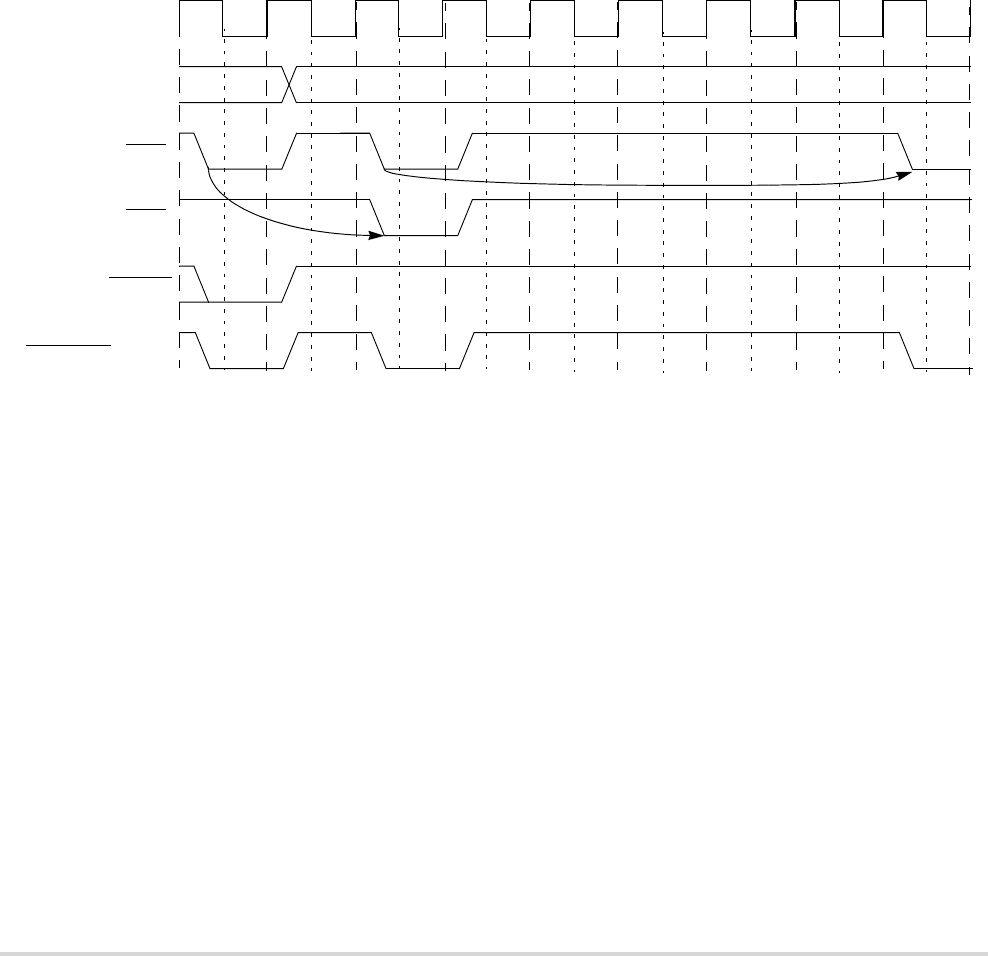
15-16 MCF5282 User’s Manual MOTOROLA
SDRAM Controller Operation
request flag. This refresh cycle includes a delay from any precharge to the auto-refresh
command, the auto-refresh command, and then a delay until any ACTV command is
allowed. Any SDRAM access initiated during the auto-refresh cycle is delayed until the
cycle is completed.
Figure 15-8 shows the auto-refresh timing. In this case, there is an SDRAM access when
the refresh request becomes active. The request is delayed by the precharge to ACTV delay
programmed into the active SDRAM bank by the CAS bits. The REF command is then
generated and the delay required by DCR[RTIM] is inserted before the next ACTV
command is generated. In this example, the next bus cycle is initiated, but does not generate
an SDRAM access until TRC is finished. Because both chip selects are active during the REF
command, it is passed to both blocks of external SDRAM.
Figure 15-8. Auto-Refresh Operation
15.2.3.6 Self-Refresh Operation
Self-refresh is a method of allowing the SDRAM to enter into a low-power state, while at
the same time to perform an internal refresh operation and to maintain the integrity of the
data stored in the SDRAM. The DRAM controller supports self-refresh with DCR[IS].
When IS is set, the SELF command is sent to the SDRAM. When IS is cleared, the SELFX
command is sent to the DRAM controller. Figure 15-9 shows the self-refresh operation.
A[31:0]
SRAS
SCAS
DRAMW
PALL
SDRAM_CS[0] or [1]
REF ACT
V
tRCD = 2
tRC = 6
CLKOUT
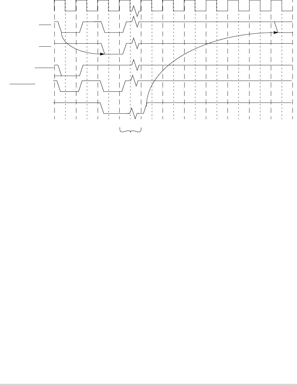
MOTOROLA Chapter 15. Synchronous DRAM Controller Module 15-17
SDRAM Controller Operation
Figure 15-9. Self-Refresh Operation
15.2.4 Initialization Sequence
Synchronous DRAMs have a prescribed initialization sequence. The DRAM controller
supports this sequence with the following procedure:
1. SDRAM control signals are reset to idle state. Wait the prescribed period after reset
before any action is taken on the SDRAMs. This is normally around 100 µs.
2. Initialize the DCR, DACR, and DMR in their operational configuration. Do not yet
enable PALL or REF commands.
3. Issue a PALL command to the SDRAMs by setting DACR[IP] and accessing a
SDRAM location. Wait the time (determined by tRP) before any other execution.
4. Enable refresh (set DACR[RE]) and wait for at least 8 refreshes to occur.
5. Before issuing the MRS command, determine if the DMR mask bits need to be
modified to allow the MRS to execute properly
6. Issue the MRS command by setting DACR[IMRS] and accessing a location in the
SDRAM. Note that mode register settings are driven on the SDRAM address bus,
so care must be taken to change DMR[BAM] if the mode register configuration
does not fall in the address range determined by the address mask bits. After the
mode register is set, DMR mask bits can be restored to their desired configuration.
SRAS
SCAS
DRAMW
PALL
SDRAM_CS[0] or [1]
SELF First
SCKE
Possible
ACTV
SELFX
Self-
Refresh
Active
tRCD = 2 tRC = 6
CLKOUT
(DCR[COC] = 0)

15-18 MCF5282 User’s Manual MOTOROLA
SDRAM Controller Operation
15.2.4.1 Mode Register Settings
It is possible to configure the operation of SDRAMs, namely their burst operation and CAS
latency, through the SDRAM component’s mode register. CAS latency is a function of the
speed of the SDRAM and the bus clock of the DRAM controller. The DRAM controller
operates at a CAS latency of 1, 2, or 3.
Although the MCF5282 DRAM controller supports bursting operations, it does not use the
bursting features of the SDRAMs. Because the MCF5282 can burst operand sizes of 1, 2,
4, or 16 bytes long, the concept of a fixed burst length in the SDRAMs mode register
becomes problematic. Therefore, the MCF5282 DRAM controller generates the burst
cycles rather than the SDRAM device. Because the MCF5282 generates a new address and
a READ or WRITE command for each transfer within the burst, the SDRAM mode register
should be set either not to burst or to a burst length of one. This allows bursting to be
controlled by the MCF5282.
The SDRAM mode register is written by setting the associated block’s DACR[IMRS].
First, the base address and mask registers must be set to the appropriate configuration to
allow the mode register to be set. Note that improperly set DMR mask bits may prevent
access to the mode register address. Thus, the user should determine the mapping of the
mode register address to the MCF5282 address bits to find out if an access is blocked. If the
DMR setting prohibits mode register access, the DMR should be reconfigured to enable the
access and then set to its necessary configuration after the MRS command executes.
The associated CBM bits should also be initialized. After DACR[IMRS] is set, the next
access to the SDRAM address space generates the MRS command to that SDRAM. The
address of the access should be selected to place the correct mode information on the
SDRAM address pins. The address is not multiplexed for the MRS command. The MRS
access can be a read or write. The important thing is that the address output of that access
needs the correct mode programming information on the correct address bits.
Figure 15-10 shows the MRS command, which occurs in the first clock of the bus cycle.
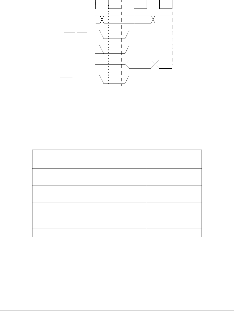
MOTOROLA Chapter 15. Synchronous DRAM Controller Module 15-19
SDRAM Example
Figure 15-10. Mode Register Set (MRS) Command
15.3 SDRAM Example
This example interfaces a 512K x 32-bit x 4 bank SDRAM component to a MCF5282
operating at 40 MHz. Table 15-25 lists design specifications for this example.
Table 15-25. SDRAM Example Specifications
Parameter Specification
Speed grade (-8E) 40 MHz (25-ns period)
10 rows, 8 columns
Two bank-select lines to access four internal banks
ACTV-to-read/write delay (tRCD) 20 ns (min.)
Period between auto-refresh and ACTV command (tRC) 70 ns
ACTV command to precharge command (tRAS) 48 ns (min.)
Precharge command to ACTV command (tRP) 20 ns (min.)
Last data input to PALL command (tRWL) 1 bus clock (25 ns)
Auto-refresh period for 4096 rows (tREF)64 mS
A[31:0]
SRAS, SCAS
DRAMW
D[31:0]
MRS
SD_CS[1] or [0]
CLKOUT

15-20 MCF5282 User’s Manual MOTOROLA
SDRAM Example
15.3.1 SDRAM Interface Configuration
To interface this component to the MCF5282 DRAM controller, use the connection table
that corresponds to a 32-bit port size with 8 columns (Table 15-24). Two pins select one of
four banks when the part is functional. Table 15-26 shows the proper hardware connections.
15.3.2 DCR Initialization
At power-up, the DCR has the following configuration if synchronous operation and
SDRAM address multiplexing are desired.
This configuration results in a value of 0x0026 for DCR, as shown in Table 15-27.
15.3.3 DACR Initialization
As shown in Figure 15-12, the SDRAM is programmed to access only the second
512-Kbyte block of each 1-Mbyte partition in the SDRAM (each 16 Mbytes). The starting
address of the SDRAM is 0xFF88_0000. Continuous page mode feature is used.
Table 15-26. SDRAM Hardware Connections
MCF5282
Pins
A15 A14 A13 A12 A11 A10 A9 A17 A18 A19 A20 A21 A22
SDRAM Pins A0 A1 A2 A3 A4 A5 A6 A7 A8 A9 A10 = CMD BA0 BA1
15 14 13 12 11 10 9 8 0
Field — — NAM COC IS RTIM RC
Setting 0000_0000_0010_0110
(hex) 0026
Figure 15-11. Initialization Values for DCR
Table 15-27. DCR Initialization Values
Bits Name Setting Description
15 — 0 Reserved.
14 — 0 Reserved.
13 NAM 0 Indicating SDRAM controller multiplexes address lines internally
12 COC 0 SCKE is used as clock enable instead of command bit because user is not multiplexing address lines
externally and requires external command feed.
11 IS 0 At power-up, allowing power self-refresh state is not appropriate because registers are being set up.
10–9 RTIM 00 Because tRC value is 70 ns, indicating a 3-clock refresh-to-ACTV timing.
8–0 RC 0x26 Specification indicates auto-refresh period for 4096 rows to be 64 mS or refresh every 15.625 µs for
each row, or 625 bus clocks at 40 MHz. Because DCR[RC] is incremented by 1 and multiplied by 16,
RC = (625 bus clocks/16) -1 = 38.06 = 0x38
MOTOROLA Chapter 15. Synchronous DRAM Controller Module 15-21
SDRAM Example
Figure 15-12. SDRAM Configuration
The DACRs should be programmed as shown in Figure 15-13.
This configuration results in a value of DACR0 = 0xFF88_0300, as described in
Table 15-28. DACR1 initialization is not needed because there is only one block.
Subsequently, DACR1[RE,IMRS,IP] should be cleared; everything else is a don’t care.
31 18 17 16
Field BA —
Setting 1111_1111_1000_10xx
(hex) F F 8 8
151413121110 876543210
Field RE — CASL — CBM — IMRS PS IP —
Setting 0000_x011_x000_0000
(hex) 0300
Figure 15-13. DACR Register Configuration
Table 15-28. DACR Initialization Values
Bits Name Setting Description
31–18 BA 1111_1111_
1000_10
Base address. So DACR0[31–16] = 0xFF88, placing the starting
address of the SDRAM accessible memory at 0xFF88_0000.
17–16 — Reserved. Don’t care.
15 RE 0 Keeps auto-refresh disabled because registers are being set up at this
time.
14 — Reserved. Don’t care.
13–12 CASL 00 Indicates a delay of data 1 cycle after SCAS is asserted
11 — Reserved. Don’t care.
10–8 CBM 011 Command bit is pin 20 and bank selects are 21 and up.
7 — Reserved. Don’t care.
6 IMRS 0 Indicates MRS command has not been initiated.
5–4 PS 00 32-bit port.
Bank 0
1 Mbyte
512 Kbyte
512 Kbyte
SDRAM Component Accessible
Memory
Bank 1
1 Mbyte
512 Kbyte
512 Kbyte
Bank 2
1 Mbyte
512 Kbyte
512 Kbyte
Bank 3
1 Mbyte
512 Kbyte
512 Kbyte

15-22 MCF5282 User’s Manual MOTOROLA
SDRAM Example
15.3.4 DMR Initialization
Again, in this example only the second 512-Kbyte block of each 1-Mbyte space is accessed
in each bank. In addition, the SDRAM component is mapped only to readable and writable
supervisor and user data. The DMRs have the following configuration.
With this configuration, the DMR0 = 0x0074_0075, as described in Table 15-29.
3 IP 0 Indicates precharge has not been initiated.
2–0 — Reserved. Don’t care.
31 18 17 16
Field BAM —
Setting 0000_0000_0111_01xx
(hex) 0 074
15 9876543210
Field — WP — C/I AM SC SD UC UD V
Setting xxxx_xxx0_x111_0101
(hex) 0075
Figure 15-14. DMR0 Register
Table 15-29. DMR0 Initialization Values
Bits Name Setting Description
31–18 BAM With bits 17 and 16 as don’t cares, BAM = 0x0074, which leaves bank select bits and upper 512K
select bits unmasked. Note that bits 22 and 21 are set because they are used as bank selects; bit 20 is
set because it controls the 1-Mbyte boundary address.
17–16 — Reserved. Don’t care.
15–9 — Reserved. Don’t care.
8 WP 0 Allow reads and writes
7 — Reserved. Don’t care.
6 C/I 1 Disable CPU space access.
5 AM 1 Disable alternate master access.
4 SC 1 Disable supervisor code accesses.
3 SD 0 Enable supervisor data accesses.
2 UC 1 Disable user code accesses.
1 UD 0 Enable user data accesses.
0 V 1 Enable accesses.
Table 15-28. DACR Initialization Values (continued)
Bits Name Setting Description
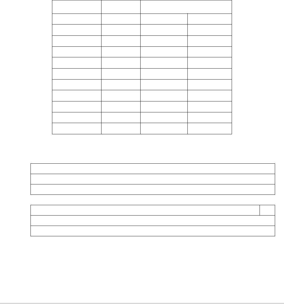
MOTOROLA Chapter 15. Synchronous DRAM Controller Module 15-23
SDRAM Example
15.3.5 Mode Register Initialization
When DACR[IMRS] is set, a bus cycle initializes the mode register. If the mode register
setting is read on A[10:0] of the SDRAM on the first bus cycle, the bit settings on the
corresponding MCF5282 address pins must be determined while being aware of masking
requirements.
Table 15-30 lists the desired initialization setting:
Next, this information is mapped to an address to determine the hexadecimal value.
Although A[31:20] corresponds to the address programmed in DACR0, according to how
DACR0 and DMR0 are initialized, bit 19 must be set to hit in the SDRAM. Thus, before
the mode register bit is set, DMR0[19] must be set to enable masking.
Table 15-30. Mode Register Initialization
MCF5282 Pins SDRAM Pins Mode Register Initialization
A20 A10 Reserved X
A19 A9 WB 0
A18 A8 Opmode 0
A17 A7 Opmode 0
A9 A6 CASL 0
A10 A5 CASL 0
A11 A4 CASL 1
A12 A3 BT 0
A13 A2 BL 0
A14 A1 BL 0
A15 A0 BL 0
31 30 29 28 27 26 25 24 23 22 21 20 19 18 17 16
Field
Setting xxxx_xxxx_xxxx_000x
(hex) 0000
1514131211109876543210
Field V
Setting 0000_100x_xxxx_xxxx
(hex) 0800
Table 15-31. Mode Register Mapping to MCF5282 A[31:0]

15-24 MCF5282 User’s Manual MOTOROLA
SDRAM Example
15.3.6 Initialization Code
The following assembly code initializes the SDRAM example.
Power-Up Sequence:
move.w #0x0026, d0//Initialize DCR
move.w d0, DCR
move.l #0xFF880300, d0 //Initialize DACR0
move.l d0, DACR0
move.l #0x00740075, d0//Initialize DMR0
move.l d0, DMR0
Precharge Sequence:
move.l #0xFF880308, d0//Set DACR0[IP]
move.l d0, DACR0
move.l #0xBEADDEED, d0//Write and value to memory location to init. precharge
move.l d0, 0xFF880000
Refresh Sequence:
move.l #0xFF888300, d0//Enable refresh bit in DACR0
move.l d0, DACR0
Mode Register Initialization Sequence:
move.l #0x00600075, d0//Mask bit 19 of address
move.l d0, DMR0
move.l #0xFF888340, d0//Enable DACR0[IMRS]; DACR0[RE] remains set
move.l d0, DACR0
move.l #0x00000000, d0//Access SDRAM address to initialize mode register
move.l d0, 0xFF800800

MOTOROLA Chapter 15. Synchronous DRAM Controller Module 15-25
SDRAM Example

15-26 MCF5282 User’s Manual MOTOROLA
SDRAM Example

MOTOROLA Chapter 16. DMA Controller Module 16-1
Chapter 16
DMA Controller Module
This chapter describes the MCF5282 Direct Memory Access (DMA) controller module. It
provides an overview of the module and describes in detail its signals and registers. The
latter sections of this chapter describe operations, features, and supported data transfer
modes in detail.
NOTE
The designation “n” is used throughout this section to refer to
registers or signals associated with one of the four identical
DMA channels: DMA0, DMA1, DMA2 or DMA3.
16.1 Overview
The DMA controller module provides an efficient way to move blocks of data with minimal
processor interaction. The DMA module, shown in Figure 16-1, provides four channels that
allow byte, word, longword, or 16-byte burst data transfers. Each channel has a dedicated
source address register (SARn), destination address register (DARn), byte count register
(BCRn), control register (DCRn), and status register (DSRn). Transfers are dual address to
on-chip devices, such as UART, SDRAM controller, and GPIOs.
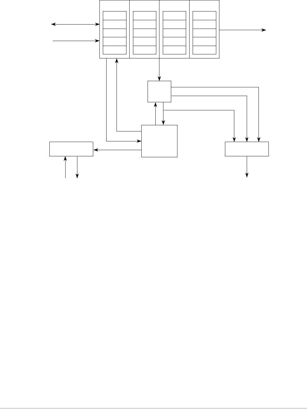
16-2 MCF5282 User’s Manual MOTOROLA
Overview
Figure 16-1. DMA Signal Diagram
NOTE
Throughout this chapter “external request” and DREQ are used
to refer to a DMA request from one of the on-chip UARTS or
DMA timers. For details on the connections associated with
DMA request inputs, see Section 16.2, “DMA Request Control
(DMAREQC).”
16.1.1 DMA Module Features
The DMA controller module features are as follows:
• Four independently programmable DMA controller channels
• Auto-alignment feature for source or destination accesses
• Dual-address transfers
• Channel arbitration on transfer boundaries
• Data transfers in 8-, 16-, 32-, or 128-bit blocks using a 16-byte buffer
• Continuous-mode or cycle-steal transfers
• Independent transfer widths for source and destination
• Independent source and destination address registers
MUX
Arbitration/
Bus Interface
Data Path
Control
Internal
External
ChannelChannel
MUX
Registered
Data Path
SAR0
DAR0
BCR0
DCR0
DSR0
Channel 0
Interrupts
SAR1
DAR1
BCR1
DCR1
DSR1
Channel 1
SAR2
DAR2
BCR2
DCR2
DSR2
Channel 2
SAR3
DAR3
BCR3
DCR3
DSR3
Channel 3
Bus
Requests
Attributes
Current Master Attributes
Write Data BusRead Data Bus
System Bus Address
System Bus Size
Channel
Enables
Requests
Bus Signals
Control
Control

MOTOROLA Chapter 16. DMA Controller Module 16-3
DMA Request Control (DMAREQC)
16.2 DMA Request Control (DMAREQC)
The DMAREQC register provides a software-controlled connection matrix for DMA
requests. It logically routes DMA requests from the DMA timers and UARTs to the four
channels of the DMA controller. Writing to this register determines the exact routing of the
DMA request to the four channels of the DMA modules. If DCRn[EEXT] is set and the
channel is idle, the assertion of the appropriate DREQn activates channel n.
31 20 19 16
Field — —
Reset 0000_0000_0000_0000
R/W R/W
15 12 11 8 7 4 3 0
Field DMAC3 DMAC2 DMAC1 DMAC0
Reset 0000_0000_0000_0000
R/W R/W
IPSBAR + 0x014
Figure 16-2. DMA Request Control Register (DMAREQC)
Table 16-1. DMAREQC Field Description
Bits Name Description
31–16 — Reserved. Should be cleared.
15–0 DMACnDMA Channel n. Each four bit field defines the logical connection between the DMA requestors and that DMA
channel. There are seven possible requesters (4 DMA Timers and 3 UARTs). Any request can be routed to any
of the DMA channels. Effectively, the DMAREQC provides a software-controlled routing matrix of the 7
DMA request signals to the 4 channels of the DMA module. DMAC3 controls DMA channel 3. DMAC2
controls DMA channel 2. DMAC1 controls DMA channel 1. DMAC0 controls DMA channel 0.
1000 UART0.
1001 UART1.
1010 UART2.
0100 DMA Timer 0.
0101 DMA Timer 1.
0110 DMA Timer 2.
0111 DMA Timer 3.
All other values are reserved and will not generate a DMA request.
16-4 MCF5282 User’s Manual MOTOROLA
DMA Transfer Overview
16.3 DMA Transfer Overview
The DMA module can transfer data faster than the ColdFire core. The term “direct memory
access” refers to a fast method of moving data within system memory (including memory
and peripheral devices) with minimal processor intervention, greatly improving overall
system performance. The DMA module consists of four independent, functionally
equivalent channels, so references to DMA in this chapter apply to any of the channels. It
is not possible to implicitly address all four channels at once.
The processor generates DMA requests internally by setting DCR[START]; the UART
modules and DMA timers can generate a DMA request by asserting internal DREQ signals.
The processor can program bus bandwidth for each channel. The channels support
cycle-steal and continuous transfer modes; see Section 16.5.1, “Transfer Requests
(Cycle-Steal and Continuous Modes).”
The DMA controller supports dual-address transfers. The DMA channels support up to 32
data bits.
• Dual-address transfers—A dual-address transfer consists of a read followed by a
write and is initiated by an internal request using the START bit or by asserting
DREQ. Two types of transfer can occur: a read from a source device or a write to a
destination device. See Figure 16-3 for more information.
Figure 16-3. Dual-Address Transfer
Any operation involving the DMA module follows the same three steps:
1. Channel initialization—Channel registers are loaded with control information,
address pointers, and a byte-transfer count.
2. Data transfer—The DMA accepts requests for operand transfers and provides
addressing and bus control for the transfers.
3. Channel termination—Occurs after the operation is finished, either successfully or
due to an error. The channel indicates the operation status in the channel’s DSR,
described in Section 16.4.5, “DMA Status Registers (DSR0–DSR3).”
DMADMA
Memory/
Peripheral
Memory/
Peripheral
Control and Data
Control and Data

MOTOROLA Chapter 16. DMA Controller Module 16-5
DMA Controller Module Programming Model
16.4 DMA Controller Module Programming Model
This section describes each internal register and its bit assignment. Note that modifying
DMA control registers during a DMA transfer can result in undefined operation. Table 16-2
shows the mapping of DMA controller registers. Note the differences for the byte count
registers depending on the value of MPARK[BCR24BIT]. See Section 8.5.3, “Bus Master
Park Register (MPARK)” for further information.
Table 16-2. Memory Map for DMA Controller Module Registers
DMA
Channel
IPSBAR
Offset [31:24] [23:16] [15:8] [7:0]
0 0x100 Source address register 0 (SAR0) [p. 16-6]
0x104 Destination address register 0 (DAR0) [p. 16-6]
0x108 DMA control register 0 (DCR0) [p. 16-8]
0x10C Byte count register 0 (BCR24BIT = 0) 1
1The DMA module originally supported a left-justified 16-bit byte count register (BCR). This function was later reimplemented as
a right-justified 24-bit BCR. The operation of the DMA and the interpretation of the BCR is controlled by the
MPARK[BCR24BIT]. See Section 8.5.3, “Bus Master Park Register (MPARK)" for more details.
Reserved
0x10C Reserved Byte count register 0 (BCR24BIT = 1) 1 (BCR0) [p. 16-7]
0x110 DMA status register 0
(DSR0) [p. 16-10]
Reserved
1 0x140 Source address register 1 (SAR1) [p. 16-6]
0x144 Destination address register 1 (DAR1) [p. 16-6]
0x148 DMA control register 1 (DCR1) [p. 16-8]
0x14C Byte count register 1 (BCR24BIT = 0) 1Reserved
0x14C Reserved Byte count register 1 (BCR24BIT = 1) 1 (BCR1) [p. 16-7]
0x150 DMA status register 1
(DSR1) [p. 16-10]
Reserved
2 0x180 Source address register 2 (SAR2) [p. 16-6]
0x184 Destination address register 2 (DAR2) [p. 16-6]
0x188 DMA control register 2 (DCR2) [p. 16-8]
0x18C Byte count register 2 (BCR24BIT = 0) 1Reserved
0x18C Reserved Byte count register 2 (BCR24BIT = 1) 1 (BCR2) [p. 16-7]
0x190 DMA status register 2
(DSR2) [p. 16-10]
Reserved
3 0x1C0 Source address register 3 (SAR3) [p. 16-6]
0x1C4 Destination address register 3 (DAR3) [p. 16-6]
0x1C8 DMA control register 3 (DCR3) [p. 16-8]
0x1CC Byte count register 3 (BCR24BIT = 0)1Reserved
0x1CC Reserved Byte count register 3 (BCR24BIT = 1)1 (BCR3) [p. 16-7]
0x1D0 DMA status register 3
(DSR3) [p. 16-10]
Reserved

16-6 MCF5282 User’s Manual MOTOROLA
DMA Controller Module Programming Model
16.4.1 Source Address Registers (SAR0–SAR3)
SARn, shown in Figure 16-4, contains the address from which the DMA controller requests
data.
NOTE
The backdoor enable bit must be set in both the core and SCM
in order to enable backdoor accesses from the DMA to SRAM.
See Section 8.4.2, “Memory Base Address Register
(RAMBAR)” for more details.
NOTE
Flash accesses (reads/writes) by a bus master other than the
core (DMA controller or Fast Ethernet Controller), or writes to
Flash by the core during programming, must use the backdoor
Flash address of IPSBAR plus an offset of 0x0400_0000. For
example, for a DMA transfer from the first Flash location when
IPSBAR is still at its default location of 0x4000_0000, the
source register would be loaded with 0x4400_0000. Backdoor
Flash read accesses can be made with the bus master, but it
takes two cycles longer than a direct read of the Flash when
using the FLASHBAR address.
16.4.2 Destination Address Registers (DAR0–DAR3)
DARn, shown in Figure 16-5, holds the address to which the DMA controller sends data.
Figure 16-5. Destination Address Registers (DARn)
31 0
Field SAR
Reset 0000_0000_0000_0000_0000_0000_0000_0000
R/W R/W
Address IPSBAR + 0x100, 0x140, 0x180, 0x1C0
Figure 16-4. Source Address Registers (SARn)
31 0
Field DAR
Reset 0000_0000_0000_0000_0000_0000_0000_0000
R/W R/W
Address IPSBAR + 0x104, 0x144, 0x184, 0x1C4

MOTOROLA Chapter 16. DMA Controller Module 16-7
DMA Controller Module Programming Model
NOTE
The DMA does not maintain coherency with the MCF5282
cache. Therefore, DMAs should not transfer data to cacheable
memory unless software is used to maintain the cache
coherency.
NOTE
The DMA should not be used to write data to the UART
transmit FIFO in cycle steal mode. When the UART interrupt
is used as a DMA request it does not negate fast enough to get
a single transfer. The UART transmit FIFO only has one entry
so the data from the second byte would be lost.
16.4.3 Byte Count Registers (BCR0–BCR3)
BCRn, shown in Figure 16-6 and Figure 16-7, hold the number of bytes yet to be
transferred for a given block. The offset within the memory map is based on the value of
MPARK[BCR24BIT]. BCRn decrements on the successful completion of the address
transfer of a write transfer. BCRn decrements by 1, 2, 4, or 16 for byte, word, longword, or
line accesses, respectively.
Figure 16-6 shows BCRn for BCR24BIT = 1.
Figure 16-6. Byte Count Registers (BCRn)—BCR24BIT = 1
Figure 16-7 shows BCRn for BCR24BIT = 0.
Figure 16-7. Byte Count Registers (BCRn)—BCR24BIT = 0
DSRn[DONE], shown in Figure 16-9, is set when the block transfer is complete.
31 24 23 0
Field — BCR
Reset — 0000_0000_0000_0000_0000_0000
R/W R/W
Address IPSBAR + 0x10C, 0x14C, 0x18C, 0x1CC
15 0
Field BCR
Reset 0000_0000_0000_0000
R/W R/W
Address IPSBAR + 0x10C, 0x14C, 0x18C, 0x1CC

16-8 MCF5282 User’s Manual MOTOROLA
DMA Controller Module Programming Model
When a transfer sequence is initiated and BCRn[BCR] is not a multiple of 16, 4, or 2 when
the DMA is configured for line, longword, or word transfers, respectively, DSRn[CE] is set
and no transfer occurs. See Section 16.4.5, “DMA Status Registers (DSR0–DSR3).”
16.4.4 DMA Control Registers (DCR0–DCR3)
DCRn, shown in Figure 16-8, is used for configuring the DMA controller module. Note
that DCRn[AT] is available only if MPARK[BCR24BIT] is set. See Section 8.5.3, “Bus
Master Park Register (MPARK)” for more information.
Table 16-3 describes DCRn fields.
31 30 29 28 27 25 24 23 22 21 20 19 18 17 16
Field INT EEXT CS AA BWC — — SINC SSIZE DINC DSIZE START
Reset 0000_0000_0000_0000
R/W R/W
15 14 0
Field AT 1
1Available only if BCR24BIT = 1, otherwise reserved.
—
Reset 0 N/A
R/W R/W
Address IPSBAR + 0x108, 0x148, 0x188, 0x1C8
Figure 16-8. DMA Control Registers (DCRn)
Table 16-3. DCRn Field Descriptions
Bits Name Description
31 INT Interrupt on completion of transfer. Determines whether an interrupt is generated by completing a transfer or by
the occurrence of an error condition.
0 No interrupt is generated.
1 Internal interrupt signal is enabled.
30 EEXT Enable external request. Care should be taken because a collision can occur between the START bit and DREQ
when EEXT = 1.
0 External request is ignored.
1 Enables external request to initiate transfer. The internal request (initiated by setting the START bit) is
always enabled.
29 CS Cycle steal.
0 DMA continuously makes read/write transfers until the BCR decrements to 0.
1 Forces a single read/write transfer per request. The request may be internal by setting the START bit, or
external by asserting DREQ.
28 AA Auto-align. AA and SIZE determine whether the source or destination is auto-aligned, that is, transfers are
optimized based on the address and size. See Section 16.5.4.1, “Auto-Alignment.”
0 Auto-align disabled
1 If SSIZE indicates a transfer no smaller than DSIZE, source accesses are auto-aligned; otherwise, destination
accesses are auto-aligned. Source alignment takes precedence over destination alignment. If auto-alignment
is enabled, the appropriate address register increments, regardless of DINC or SINC.

MOTOROLA Chapter 16. DMA Controller Module 16-9
DMA Controller Module Programming Model
27–25 BWC Bandwidth control. Indicates the number of bytes in a block transfer. When the byte count reaches a multiple
of the BWC value, the DMA releases the bus. For example, if BCR24BIT is 0, BWC is 001 (512 bytes or value
of 0x0200), and BCR is 0x1000, the bus is relinquished after BCR values of 0x0E00, 0x0C00, 0x0A00, 0x0800,
0x0600, 0x0400, and 0x0200. If BCR24BIT is 0, BWC is 110, and BCR is 33000, the bus is released after 232
bytes because the BCR is at 32768, a multiple of 16384.
24-23 — Reserved, should be cleared.
22 SINC Source increment. Controls whether a source address increments after each successful transfer.
0 No change to SAR after a successful transfer.
1 The SAR increments by 1, 2, 4, or 16, as determined by the transfer size.
21–20 SSIZE Source size. Determines the data size of the source bus cycle for the DMA control module.
00 Longword
01 Byte
10 Word
11 Line (16-byte burst)
19 DINC Destination increment. Controls whether a destination address increments after each successful transfer.
0 No change to the DAR after a successful transfer.
1 The DAR increments by 1, 2, 4, or 16, depending upon the size of the transfer.
18–17 DSIZE Destination size. Determines the data size of the destination bus cycle for the DMA controller.
00 Longword
01 Byte
10 Word
11 Line (16-byte burst)
16 START Start transfer.
0 DMA inactive
1 The DMA begins the transfer in accordance to the values in the control registers. START is cleared
automatically after one system clock and is always read as logic 0.
Table 16-3. DCRn Field Descriptions (continued)
Bits Name Description
Encoding BCR24BIT = 0 BCR24BIT = 1
000 DMA has priority and does not negate its request
until transfer completes.
001 512 16384
010 1024 32768
011 2048 65536
100 4096 131072
101 8192 262144
110 16384 524288
111 32768 1048576

16-10 MCF5282 User’s Manual MOTOROLA
DMA Controller Module Programming Model
16.4.5 DMA Status Registers (DSR0–DSR3)
In response to an event, the DMA controller writes to the appropriate DSRn bit,
Figure 16-9. Only a write to DSRn[DONE] results in action.
Table 16-4 describes DSRn fields.
15 AT AT is available only if MPARK[BCR24BIT] = 1.
DMA acknowledge type. Controls whether acknowledge information is provided for the entire transfer or only
the final transfer.
0 Entire transfer. DMA acknowledge information is displayed anytime the channel is selected as the result of
an external request.
1 Final transfer (when BCR reaches zero). For dual-address transfer, the acknowledge information is displayed
for both the read and write cycles.
14–0 — Reserved, should be cleared.
76543210
Field — CE BES BED — REQ BSY DONE
Reset 0000_0000
R/W R/W
Address IPSBAR + 0x110, 0x150, 0x190, 0x1D0
Figure 16-9. DMA Status Registers (DSRn)
Table 16-4. DSRn Field Descriptions
Bits Name Description
7 — Reserved, should be cleared.
6 CE Configuration error. Occurs when BCR, SAR, or DAR does not match the requested transfer size, or if BCR
= 0 when the DMA receives a start condition. CE is cleared at hardware reset or by writing a 1 to DSR[DONE].
0 No configuration error exists.
1 A configuration error has occurred.
5 BES Bus error on source
0 No bus error occurred.
1 The DMA channel terminated with a bus error during the read portion of a transfer.
4 BED Bus error on destination
0 No bus error occurred.
1 The DMA channel terminated with a bus error during the write portion of a transfer.
3 — Reserved, should be cleared.
2 REQ Request
0 No request is pending or the channel is currently active. Cleared when the channel is selected.
1 The DMA channel has a transfer remaining and the channel is not selected.
Table 16-3. DCRn Field Descriptions (continued)
Bits Name Description

MOTOROLA Chapter 16. DMA Controller Module 16-11
DMA Controller Module Functional Description
16.5 DMA Controller Module Functional Description
In the following discussion, the term “DMA request” implies that DCRn[START] or
DCRn[EEXT] is set, followed by assertion of DREQn. The START bit is cleared when the
channel begins an internal access.
Before initiating a dual-address access, the DMA module verifies that
DCRn[SSIZE,DSIZE] are consistent with the source and destination addresses. If they are
not consistent, the configuration error bit, DSRn[CE], is set. If misalignment is detected, no
transfer occurs, DSRn[CE] is set, and, depending on the DCR configuration, an interrupt
event is issued. Note that if the auto-align bit, DCRn[AA], is set, error checking is
performed on the appropriate registers.
A read/write transfer reads bytes from the source address and writes them to the destination
address. The number of bytes is the larger of the sizes specified by DCRn[SSIZE] and
DCRn[DSIZE]. See Section 16.4.4, “DMA Control Registers (DCR0–DCR3).”
Source and destination address registers (SARn and DARn) can be programmed in the
DCRn to increment at the completion of a successful transfer. BCRn decrements when an
address transfer write completes for a single-address access (DCRn[SAA] = 0) or when
SAA = 1.
16.5.1 Transfer Requests (Cycle-Steal and
Continuous Modes)
The DMA channel supports internal and external requests. A request is issued by setting
DCRn[START] or by asserting DREQn. Setting DCRn[EEXT] enables recognition of
external DMA requests. Selecting between cycle-steal and continuous modes minimizes
bus usage for either internal or external requests.
• Cycle-steal mode (DCRn[CS] = 1)—Only one complete transfer from source to
destination occurs for each request. If DCRn[EEXT] is set, a request can be either
internal or external. An internal request is selected by setting DCRn[START]. An
1BSYBusy
0 DMA channel is inactive. Cleared when the DMA has finished the last transaction.
1 BSY is set the first time the channel is enabled after a transfer is initiated.
0 DONE Transactions done. Set when all DMA controller transactions complete, as determined by transfer count or
error conditions. When BCR reaches zero, DONE is set when the final transfer completes successfully. DONE
can also be used to abort a transfer by resetting the status bits. When a transfer completes, software must clear
DONE before reprogramming the DMA.
0 Writing or reading a 0 has no effect.
1 DMA transfer completed. Writing a 1 to this bit clears all DMA status bits and can be used in an interrupt
handler to clear the DMA interrupt and error bits.
Table 16-4. DSRn Field Descriptions (continued)
Bits Name Description

16-12 MCF5282 User’s Manual MOTOROLA
DMA Controller Module Functional Description
external request is initiated by asserting DREQn while DCRn[EEXT] is set. Note
that multiple transfers will occur if DREQn is continuously asserted.
• Continuous mode (DCRn[CS] = 0)—After an internal or external request, the DMA
continuously transfers data until BCRn reaches zero or a multiple of DCRn[BWC]
or until DSRn[DONE] is set. If BCRn is a multiple of BWC, the DMA request signal
is negated until the bus cycle terminates to allow the internal arbiter to switch
masters. DCRn[BWC] = 000 specifies the maximum transfer rate; other values
specify a transfer rate limit.
The DMA performs the specified number of transfers, then relinquishes bus control.
The DMA negates its internal bus request on the last transfer before BCRn reaches
a multiple of the boundary specified in BWC. On completion, the DMA reasserts its
bus request to regain mastership at the earliest opportunity. The DMA loses bus
control for a minimum of one bus cycle.
16.5.2 Data Transfer Modes
Each channel supports dual-address transfers, described in the next section.
16.5.2.1 Dual-Address Transfers
Dual-address transfers consist of a source data read and a destination data write. The DMA
controller module begins a dual-address transfer sequence during a DMA request. If no
error condition exists, DSRn[REQ] is set.
• Dual-address read—The DMA controller drives the SARn value onto the internal
address bus. If DCRn[SINC] is set, the SARn increments by the appropriate number
of bytes upon a successful read cycle. When the appropriate number of read cycles
complete (multiple reads if the destination size is larger than the source), the DMA
initiates the write portion of the transfer.
If a termination error occurs, DSRn[BES,DONE] are set and DMA transactions
stop.
• Dual-address write—The DMA controller drives the DARn value onto the address
bus. If DCRn[DINC] is set, DARn increments by the appropriate number of bytes at
the completion of a successful write cycle. BCRn decrements by the appropriate
number of bytes. DSRn[DONE] is set when BCRn reaches zero. If the BCRn is
greater than zero, another read/write transfer is initiated. If the BCRn is a multiple
of DCRn[BWC], the DMA request signal is negated until termination of the bus
cycle to allow the internal arbiter to switch masters.
If a termination error occurs, DSRn[BES,DONE] are set and DMA transactions
stop.

MOTOROLA Chapter 16. DMA Controller Module 16-13
DMA Controller Module Functional Description
16.5.3 Channel Initialization and Startup
Before a block transfer starts, channel registers must be initialized with information
describing configuration, request-generation method, and the data block.
16.5.3.1 Channel Prioritization
The four DMA channels are prioritized in ascending order (channel 0 having highest
priority and channel 3 having the lowest) or in an order determined by DCRn[BWC]. If the
BWC encoding for a DMA channel is 000, that channel has priority only over the channel
immediately preceding it. For example, if DCR3[BWC] = 000, DMA channel 3 has priority
over DMA channel 2 (assuming DCR2[BWC] ≠ 000) but not over DMA channel 1.
If DCR0[BWC] = DCR1[BWC] = 000, DMA0 still has priority over DMA1. In this case,
DCR1[BWC] = 000 does not affect prioritization.
Simultaneous external requests are prioritized either in ascending order or in an order
determined by each channel’s DCRn[BWC] bits.
16.5.3.2 Programming the DMA Controller Module
Note the following general guidelines for programming the DMA:
• No mechanism exists within the DMA module itself to prevent writes to control
registers during DMA accesses.
• If the DCRn[BWC] value of sequential channels are equal, the channels are
prioritized in ascending order.
The SARn is loaded with the source (read) address. If the transfer is from a peripheral
device to memory, the source address is the location of the peripheral data register. If the
transfer is from memory to either a peripheral device or memory, the source address is the
starting address of the data block. This can be any aligned byte address.
The DARn should contain the destination (write) address. If the transfer is from a peripheral
device to memory, or from memory to memory, the DARn is loaded with the starting
address of the data block to be written. If the transfer is from memory to a peripheral device,
DARn is loaded with the address of the peripheral data register. This address can be any
aligned byte address.
SARn and DARn change after each cycle depending on DCRn[SSIZE,DSIZE,
SINC,DINC] and on the starting address. Increment values can be 1, 2, 4, or 16 for byte,
word, longword, or 16-byte line transfers, respectively. If the address register is
programmed to remain unchanged (no count), the register is not incremented after the data
transfer.

16-14 MCF5282 User’s Manual MOTOROLA
DMA Controller Module Functional Description
BCRn[BCR] must be loaded with the number of byte transfers to occur. It is decremented
by 1, 2, 4, or 16 at the end of each transfer, depending on the transfer size. DSRn[DONE]
must be cleared for channel startup.
As soon as the channel has been initialized, it is started by writing a one to DCRn[START]
or asserting DREQn, depending on the status of DCRn[EEXT]. Programming the channel
for internal requests causes the channel to request the bus and start transferring data
immediately. If the channel is programmed for external request, DREQn must be asserted
before the channel requests the bus.
Changes to DCRn are effective immediately while the channel is active. To avoid problems
with changing a DMA channel setup, write a one to DSRn[DONE] to stop the DMA
channel.
16.5.4 Data Transfer
This section describes auto-alignment and bandwidth control for DMA transfers.
16.5.4.1 Auto-Alignment
Auto-alignment allows block transfers to occur at the optimal size based on the address,
byte count, and programmed size. To use this feature, DCRn[AA] must be set. The source
is auto-aligned if DCRn[SSIZE] indicates a transfer size larger than DCRn[DSIZE]. Source
alignment takes precedence over the destination when the source and destination sizes are
equal. Otherwise, the destination is auto-aligned. The address register chosen for alignment
increments regardless of the increment value. Configuration error checking is performed on
registers not chosen for alignment.
If BCRn is greater than 16, the address determines transfer size. Bytes, words, or longwords
are transferred until the address is aligned to the programmed size boundary, at which time
accesses begin using the programmed size.
If BCRn is less than 16 at the start of a transfer, the number of bytes remaining dictates
transfer size. For example, AA = 1, SARn = 0x0001, BCRn = 0x00F0, SSIZE = 00
(longword), and DSIZE = 01 (byte). Because SSIZE > DSIZE, the source is auto-aligned.
Error checking is performed on destination registers. The access sequence is as follows:
1. Read byte from 0x0001—write 1 byte, increment SARn.
2. Read word from 0x0002—write 2 bytes, increment SARn.
3. Read longword from 0x0004—write 4 bytes, increment SARn.
4. Repeat longwords until SARn = 0x00F0.
5. Read byte from 0x00F0—write byte, increment SARn.
If DSIZE is another size, data writes are optimized to write the largest size allowed based
on the address, but not exceeding the configured size.

MOTOROLA Chapter 16. DMA Controller Module 16-15
DMA Controller Module Functional Description
16.5.4.2 Bandwidth Control
Bandwidth control makes it possible to force the DMA off the bus to allow access to
another device. DCRn[BWC] provides seven levels of block transfer sizes. If the BCRn
decrements to a multiple of the decode of the BWC, the DMA bus request negates until the
bus cycle terminates. If a request is pending, the arbiter may then pass bus mastership to
another device. If auto-alignment is enabled, DCRn[AA] = 1, the BCRn may skip over the
programmed boundary, in which case, the DMA bus request is not negated.
If BWC = 000, the request signal remains asserted until BCRn reaches zero. DMA has
priority over the core. Note that in this scheme, the arbiter can always force the DMA to
relinquish the bus. See Section 8.5.3, “Bus Master Park Register (MPARK).”
16.5.5 Termination
An unsuccessful transfer can terminate for one of the following reasons:
• Error conditions—When the MCF5282 encounters a read or write cycle that
terminates with an error condition, DSRn[BES] is set for a read and DSRn[BED] is
set for a write before the transfer is halted. If the error occurred in a write cycle, data
in the internal holding register is lost.
• Interrupts—If DCRn[INT] is set, the DMA drives the appropriate internal interrupt
signal. The processor can read DSRn to determine whether the transfer terminated
successfully or with an error. DSRn[DONE] is then written with a one to clear the
interrupt and the DONE and error bits.

16-16 MCF5282 User’s Manual MOTOROLA
DMA Controller Module Functional Description

MOTOROLA Chapter 17. Fast Ethernet Controller (FEC) 17-1
Chapter 17
Fast Ethernet Controller (FEC)
This chapter provides a feature-set overview, a functional block diagram, and transceiver
connection information for both the 10 and 100 Mbps MII (Media Independent Interface),
as well as the 7-wire serial interface. Additionally, detailed descriptions of operation and
the programming model are included.
17.1 Overview
The Ethernet Media Access Controller (MAC) is designed to support both 10 and 100 Mbps
Ethernet/IEEE 802.3 networks. An external transceiver interface and transceiver function
are required to complete the interface to the media. The FEC supports three different
standard MAC-PHY (physical) interfaces for connection to an external Ethernet
transceiver. The FEC supports the 10/100 Mbps MII and the 10 Mbps-only 7-wire
interface, which uses a subset of the MII pins.
17.1.1 Features
The FEC incorporates the following features:
• Support for three different Ethernet physical interfaces:
— 100-Mbps IEEE 802.3 MII
— 10-Mbps IEEE 802.3 MII
— 10-Mbps 7-wire interface (industry standard)
• IEEE 802.3 full duplex flow control
• Programmable max frame length supports IEEE 802.1 VLAN tags and priority
• Support for full-duplex operation (200Mbps throughput) with a minimum system
clock rate of 50MHz
• Support for half-duplex operation (100Mbps throughput) with a minimum system
clock rate of 25 MHz
• Retransmission from transmit FIFO following a collision (no processor bus
utilization)

17-2 MCF5282 User’s Manual MOTOROLA
Modes of Operation
• Automatic internal flushing of the receive FIFO for runts (collision fragments) and
address recognition rejects (no processor bus utilization)
• Address recognition
— Frames with broadcast address may be always accepted or always rejected
— Exact match for single 48-bit individual (unicast) address
— Hash (64-bit hash) check of individual (unicast) addresses
— Hash (64-bit hash) check of group (multicast) addresses
— Promiscuous mode
17.2 Modes of Operation
The primary operational modes are described in this section.
17.2.1 Full and Half Duplex Operation
Full duplex mode is intended for use on point to point links between switches or end node
to switch. Half duplex mode is used in connections between an end node and a repeater or
between repeaters. Selection of the duplex mode is controlled by TCR[FDEN].
When configured for full duplex mode, flow control may be enabled. Refer to the
TCR[RFC_PAUSE] and TCR[TFC_PAUSE] bits, the RCR[FCE] bit, and Section 17.4.10,
“Full Duplex Flow Control,” for more details.
17.2.2 Interface Options
The following interface options are supported. A detailed discussion of the interface
configurations is provided in Section 17.4.5, “Network Interface Options”.
17.2.2.1 10 Mbps and 100 Mbps MII Interface
MII is the Media Independent Interface defined by the IEEE 802.3 standard for 10/100
Mbps operation. The MAC-PHY interface may be configured to operate in MII mode by
asserting RCR[MII_MODE].
The speed of operation is determined by the ETXCLK and ERXCLK pins which are driven
by the external transceiver. The transceiver will either auto-negotiate the speed or it may be
controlled by software via the serial management interface (EMDC/EMDIO pins) to the
transceiver. Refer to the MMFR and MSCR register descriptions as well as the section on
the MII for a description of how to read and write registers in the transceiver via this
interface.

MOTOROLA Chapter 17. Fast Ethernet Controller (FEC) 17-3
Modes of Operation
17.2.2.2 10 Mpbs 7-Wire Interface Operation
The FEC supports a 7-wire interface as used by many 10 Mbps ethernet transceivers. The
RCR[MII_MODE] bit controls this functionality. If this bit is deasserted, the MII mode is
disabled and the 10 Mbps, 7-wire mode is enabled.
17.2.3 Address Recognition Options
The address options supported are promiscuous, broadcast reject, individual address (hash
or exact match), and multicast hash match. Address recognition options are discussed in
detail in Section 17.4.8, “Ethernet Address Recognition”.
17.2.4 Internal Loopback
Internal loopback mode is selected via RCR[LOOP]. Loopback mode is discussed in detail
in Section 17.4.13, “Internal and External Loopback”.
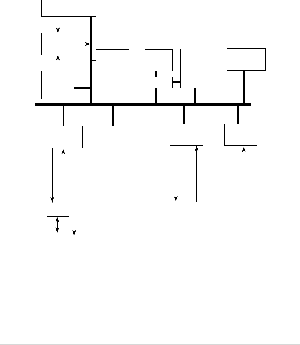
17-4 MCF5282 User’s Manual MOTOROLA
FEC Top-Level Functional Diagram
17.3 FEC Top-Level Functional Diagram
The block diagram of the FEC is shown below. The FEC is implemented with a
combination of hardware and microcode. The off-chip (Ethernet) interfaces are compliant
with industry and IEEE 802.3 standards.
Figure 17-1. FEC Block Diagram
The descriptor controller is a RISC-based controller that provides the following functions
in the FEC:
• Initialization (those internal registers not initialized by the user or hardware)
• High level control of the DMA channels (initiating DMA transfers)
• Interpreting buffer descriptors
• Address recognition for receive frames
• Random number generation for transmit collision backoff timer
SIF
CSR FIFO DMA
Descriptor
Controller
MII Receive
Transmit
Bus
Controller
Controller
EMDCEMDIO
ERXCLK
ERXDV
ERXD[3:0]
ERXER
ETCLKETXEN
ETXD[3:0]
ETXER
ECRS,ECOL
MIB
(RISC +
microcode)
I/O
PAD
MDO
MDEN MDI
Counters
MII/7-WIRE DATA
OPTION
RAM
RAM I/F
FEC Bus

MOTOROLA Chapter 17. Fast Ethernet Controller (FEC) 17-5
Functional Description
NOTE
DMA references in this section refer to the FEC’s DMA
engine. This DMA engine is for the transfer of FEC data only,
and is not related to the DMA controller described in
Chapter 16, “DMA Controller Module,” nor to the DMA
timers described in Chapter 21, “DMA Timers
(DTIM0–DTIM3).”
The RAM is the focal point of all data flow in the Fast Ethernet Controller and is divided
into transmit and receive FIFOs. The FIFO boundaries are programmable using the FRSR
register. User data flows to/from the DMA block from/to the receive/transmit FIFOs.
Transmit data flows from the transmit FIFO into the transmit block and receive data flows
from the receive block into the receive FIFO.
The user controls the FEC by writing, through the SIF (Slave Interface) module, into
control registers located in each block. The CSR (control and status register) block provides
global control (e.g. Ethernet reset and enable) and interrupt handling registers.
The MII block provides a serial channel for control/status communication with the external
physical layer device (transceiver). This serial channel consists of the EMDC (Management
Data Clock) and EMDIO (Management Data Input/Output) lines of the MII interface.
The DMA block provides multiple channels allowing transmit data, transmit descriptor,
receive data and receive descriptor accesses to run independently.
The Transmit and Receive blocks provide the Ethernet MAC functionality (with some
assist from microcode).
The Message Information Block (MIB) maintains counters for a variety of network events
and statistics. It is not necessary for operation of the FEC but provides valuable counters
for network management. The counters supported are the RMON (RFC 1757) Ethernet
Statistics group and some of the IEEE 802.3 counters. See Section 17.5.3, “MIB Block
Counters Memory Map” for more information.
17.4 Functional Description
This section describes the operation of the FEC, beginning with the hardware and software
initialization sequence, then the software (Ethernet driver) interface for transmitting and
receiving frames.
Following the software initialization and operation sections are sections providing a
detailed description of the functions of the FEC.

17-6 MCF5282 User’s Manual MOTOROLA
Functional Description
17.4.1 Initialization Sequence
This section describes which registers are reset due to hardware reset, which are reset by
the FEC RISC, and what locations the user must initialize prior to enabling the FEC.
17.4.1.1 Hardware Controlled Initialization
In the FEC, registers and control logic that generate interrupts are reset by hardware. A
hardware reset deasserts output signals and resets general configuration bits.
Other registers reset when the ECR[ETHER_EN] bit is cleared. ECR[ETHER_EN] is
deasserted by a hard reset or may be deasserted by software to halt operation. By
deasserting ECR[ETHER_EN], the configuration control registers such as the TCR and
RCR will not be reset, but the entire data path will be reset.
17.4.2 User Initialization (Prior to Asserting ECR[ETHER_EN])
The user needs to initialize portions the FEC prior to setting the ECR[ETHER_EN] bit. The
exact values will depend on the particular application. The sequence is not important.
Ethernet MAC registers requiring initialization are defined in Table 17-2.
Table 17-1. ECR[ETHER_EN] De-Assertion Effect on FEC
Register/Machine Reset Value
XMIT block Transmission is aborted (bad CRC
appended)
RECV block Receive activity is aborted
DMA block All DMA activity is terminated
RDAR Cleared
TDAR Cleared
Descriptor Controller block Halt operation
Table 17-2. User Initialization (Before ECR[ETHER_EN])
Description
Initialize EIMR
Clear EIR (write 0xFFFF_FFFF)
TFWR (optional)
IALR / IAUR
GAUR / GALR
PALR / PAUR (only needed for full duplex flow control)
OPD (only needed for full duplex flow control)
RCR
TCR

MOTOROLA Chapter 17. Fast Ethernet Controller (FEC) 17-7
Functional Description
FEC FIFO/DMA registers that require initialization are defined in Table 17-3.
17.4.3 Microcontroller Initialization
In the FEC, the descriptor control RISC initializes some registers after ECR[ETHER_EN]
is asserted. After the microcontroller initialization sequence is complete, the hardware is
ready for operation.
Table 17-4 shows microcontroller initialization operations.
17.4.4 User Initialization (After Asserting ECR[ETHER_EN])
After asserting ECR[ETHER_EN], the user can set up the buffer/frame descriptors and
write to the TDAR and RDAR. Refer to Section 17.6, “Buffer Descriptors” for more
details.
MSCR (optional)
Clear MIB_RAM (locations IPSBAR + 0x1200-0x12FC)
Table 17-3. FEC User Initialization (Before ECR[ETHER_EN])
Description
Initialize FRSR (optional)
Initialize EMRBR
Initialize ERDSR
Initialize ETDSR
Initialize (Empty) Transmit Descriptor ring
Initialize (Empty) Receive Descriptor ring
Table 17-4. Microcontroller Initialization
Description
Initialize BackOff Random Number Seed
Activate Receiver
Activate Transmitter
Clear Transmit FIFO
Clear Receive FIFO
Initialize Transmit Ring Pointer
Initialize Receive Ring Pointer
Initialize FIFO Count Registers
Table 17-2. User Initialization (Before ECR[ETHER_EN]) (continued)
Description

17-8 MCF5282 User’s Manual MOTOROLA
Functional Description
17.4.5 Network Interface Options
The FEC supports both an MII interface for 10/100 Mbps Ethernet and a 7-wire serial
interface for 10 Mbps Ethernet. The interface mode is selected by the RCR[MII_MODE]
bit. In MII mode (RCR[MII_MODE] = 1), there are 18 signals defined by the IEEE 802.3
standard and supported by the EMAC. These signals are shown in Table 17-5 below.
The 7-wire serial mode interface (RCR[MII_MODE] = 0) operates in what is generally
referred to as the “AMD” mode. 7-wire mode connections to the external transceiver are
shown in Table 17-6.
Table 17-5. MII Mode
Signal Description EMAC pin
Transmit Clock ETXCLK
Transmit Enable ETXEN
Transmit Data ETXD[3:0]
Transmit Error ETXER
Collision ECOL
Carrier Sense ECRS
Receive Clock ERXCLK
Receive Data Valid ERXDV
Receive Data ERXD[3:0]
Receive Error ERXER
Management Data Clock EMDC
Management Data
Input/Output
EMDIO
Table 17-6. 7-Wire Mode Configuration
SIGNAL DESCRIPTION EMAC PIN
Transmit Clock ETXCLK
Transmit Enable ETXEN
Transmit Data ETXD[0]
Collision ECOL
Receive Clock ERXCLK
Receive Data Valid ERXDV
Receive Data ERXD[0]

MOTOROLA Chapter 17. Fast Ethernet Controller (FEC) 17-9
Functional Description
17.4.6 FEC Frame Transmission
The Ethernet transmitter is designed to work with almost no intervention from software.
Once ECR[ETHER_EN] is asserted and data appears in the transmit FIFO, the Ethernet
MAC is able to transmit onto the network.
When the transmit FIFO fills to the watermark (defined by the TFWR), the MAC transmit
logic will assert ETXEN and start transmitting the preamble (PA) sequence, the start frame
delimiter (SFD), and then the frame information from the FIFO. However, the controller
defers the transmission if the network is busy (ECRS asserts). Before transmitting, the
controller waits for carrier sense to become inactive, then determines if carrier sense stays
inactive for 60 bit times. If so, the transmission begins after waiting an additional 36 bit
times (96 bit times after carrier sense originally became inactive). See Section 17.4.14.1,
“Transmission Errors” for more details.
If a collision occurs during transmission of the frame (half duplex mode), the Ethernet
controller follows the specified backoff procedures and attempts to retransmit the frame
until the retry limit is reached. The transmit FIFO stores at least the first 64 bytes of the
transmit frame, so that they do not have to be retrieved from system memory in case of a
collision. This improves bus utilization and latency in case immediate retransmission is
necessary.
When all the frame data has been transmitted, the FCS (Frame Check Sequence or 32-bit
Cyclic Redundancy Check, CRC) bytes are appended if the TC bit is set in the transmit
frame control word. If the ABC bit is set in the transmit frame control word, a bad CRC will
be appended to the frame data regardless of the TC bit value. Following the transmission
of the CRC, the Ethernet controller writes the frame status information to the MIB block.
Short frames are automatically padded by the transmit logic (if the TC bit in the transmit
buffer descriptor for the end of frame buffer = 1).
Both buffer (TXB) and frame (TFINT) interrupts may be generated as determined by the
settings in the EIMR.
The transmit error interrupts are HBERR, BABT, LATE_COL, COL_RETRY_LIM, and
XFIFO_UN. If the transmit frame length exceeds MAX_FL bytes the BABT interrupt will
be asserted, however the entire frame will be transmitted (no truncation).
To pause transmission, set the GTS (graceful transmit stop) bit in the TCR register. When
the TCR[GTS] is set, the FEC transmitter stops immediately if transmission is not in
progress; otherwise, it continues transmission until the current frame either finishes or
terminates with a collision. After the transmitter has stopped the GRA (graceful stop
complete) interrupt is asserted. If TCR[GTS] is cleared, the FEC resumes transmission with
the next frame.
The Ethernet controller transmits bytes least significant bit first.

17-10 MCF5282 User’s Manual MOTOROLA
Functional Description
17.4.7 FEC Frame Reception
The FEC receiver is designed to work with almost no intervention from the host and can
perform address recognition, CRC checking, short frame checking, and maximum frame
length checking.
When the driver enables the FEC receiver by asserting ECR[ETHER_EN], it will
immediately start processing receive frames. When ERXDV asserts, the receiver will first
check for a valid PA/SFD header. If the PA/SFD is valid, it will be stripped and the frame
will be processed by the receiver. If a valid PA/SFD is not found, the frame will be ignored.
In serial mode, the first 16 bit times of RX_D0 following assertion of ERXDV are ignored.
Following the first 16 bit times the data sequence is checked for alternating 1/0s. If a 11 or
00 data sequence is detected during bit times 17 to 21, the remainder of the frame is ignored.
After bit time 21, the data sequence is monitored for a valid SFD (11). If a 00 is detected,
the frame is rejected. When a 11 is detected, the PA/SFD sequence is complete.
In MII mode, the receiver checks for at least one byte matching the SFD. Zero or more PA
bytes may occur, but if a 00 bit sequence is detected prior to the SFD byte, the frame is
ignored.
After the first 6 bytes of the frame have been received, the FEC performs address
recognition on the frame.
Once a collision window (64 bytes) of data has been received and if address recognition has
not rejected the frame, the receive FIFO is signalled that the frame is “accepted” and may
be passed on to the DMA. If the frame is a runt (due to collision) or is rejected by address
recognition, the receive FIFO is notified to “reject” the frame. Thus, no collision fragments
are presented to the user except late collisions, which indicate serious LAN problems.
During reception, the Ethernet controller checks for various error conditions and once the
entire frame is written into the FIFO, a 32-bit frame status word is written into the FIFO.
This status word contains the M, BC, MC, LG, NO, CR, OV and TR status bits, and the
frame length. See Section 17.4.14.2, “Reception Errors” for more details.
Receive Buffer (RXB) and Frame Interrupts (RFINT) may be generated if enabled by the
EIMR register. A receive error interrupt is babbling receiver error (BABR). Receive frames
are not truncated if they exceed the max frame length (MAX_FL); however, the BABR
interrupt will occur and the LG bit in the Receive Buffer Descriptor (RxBD) will be set. See
Section 17.6.2, “Ethernet Receive Buffer Descriptor (RxBD)” for more details.
When the receive frame is complete, the FEC sets the L-bit in the RxBD, writes the other
frame status bits into the RxBD, and clears the E-bit. The Ethernet controller next generates
a maskable interrupt (RFINT bit in EIR, maskable by RFIEN bit in EIMR), indicating that
a frame has been received and is in memory. The Ethernet controller then waits for a new
frame.
The Ethernet controller receives serial data LSB first.

MOTOROLA Chapter 17. Fast Ethernet Controller (FEC) 17-11
Functional Description
17.4.8 Ethernet Address Recognition
The FEC filters the received frames based on destination address (DA) type — individual
(unicast), group (multicast), or broadcast (all-ones group address). The difference between
an individual address and a group address is determined by the I/G bit in the destination
address field. A flowchart for address recognition on received frames is illustrated in the
figures below.
Address recognition is accomplished through the use of the receive block and microcode
running on the microcontroller. The flowchart shown in Figure 17-2 illustrates the address
recognition decisions made by the receive block, while Figure 17-3 illustrates the decisions
made by the microcontroller.
If the DA is a broadcast address and broadcast reject (RCR[BC_REJ]) is deasserted, then
the frame will be accepted unconditionally, as shown in Figure 17-2. Otherwise, if the DA
is not a broadcast address, then the microcontroller runs the address recognition subroutine,
as shown in Figure 17-3.
If the DA is a group (multicast) address and flow control is disabled, then the
microcontroller will perform a group hash table lookup using the 64-entry hash table
programmed in GAUR and GALR. If a hash match occurs, the receiver accepts the frame.
If flow control is enabled, the microcontroller will do an exact address match check
between the DA and the designated PAUSE DA (01:80:C2:00:00:01). If the receive block
determines that the received frame is a valid PAUSE frame, then the frame will be rejected.
Note the receiver will detect a PAUSE frame with the DA field set to either the designated
PAUSE DA or the unicast physical address.
If the DA is the individual (unicast) address, the microcontroller performs an individual
exact match comparison between the DA and 48-bit physical address that the user programs
in the PALR and PAUR registers. If an exact match occurs, the frame is accepted;
otherwise, the microcontroller does an individual hash table lookup using the 64-entry hash
table programmed in registers, IAUR and IALR. In the case of an individual hash match,
the frame is accepted. Again, the receiver will accept or reject the frame based on PAUSE
frame detection, shown in Figure 17-2.
If neither a hash match (group or individual), nor an exact match (group or individual)
occur, then if promiscuous mode is enabled (RCR[PROM] = 1), then the frame will be
accepted and the MISS bit in the receive buffer descriptor is set; otherwise, the frame will
be rejected.
Similarly, if the DA is a broadcast address, broadcast reject (RCR[BC_REJ]) is asserted,
and promiscuous mode is enabled, then the frame will be accepted and the MISS bit in the
receive buffer descriptor is set; otherwise, the frame will be rejected.
In general, when a frame is rejected, it is flushed from the FIFO.
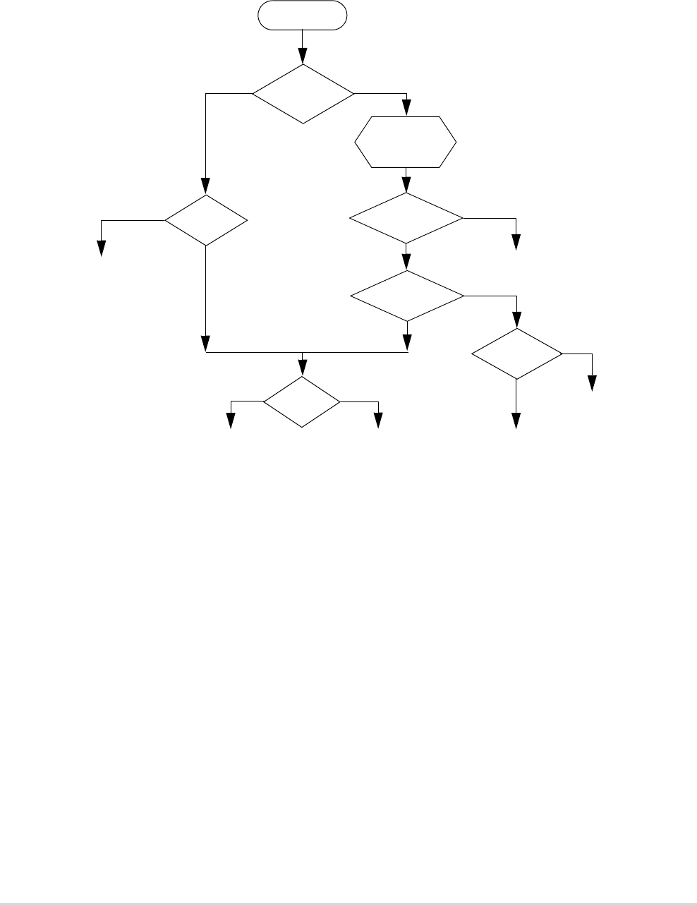
17-12 MCF5282 User’s Manual MOTOROLA
Functional Description
Figure 17-2. Ethernet Address Recognition—Receive Block Decisions
Accept/Reject
Broadcast Addr
?
?
PROM = 1
?
Receive
Address
True
NOTES:
BC_REJ - field in RCR register (BroadCast REJect)
False
True
False
BC_REJ = 1
?
Frame
Hash Match
?
Exact Match
?
Pause Frame
False
False
False
False
True
True
True
True
Receive Frame Receive Frame
Receive Frame Receive Frame
Reject Frame
Reject Frame
PROM - field in RCR register (PROMiscous mode)
Pause Frame - valid PAUSE frame received
Set BC bit in RCV BD Set MC bit in RCV BD if multicast
Set M (Miss) bit in Rcv BD
Set MC bit in Rcv BD if multicast
Set BC bit in Rcv BD if broadcast
Flush from FIFO
Flush from FIFO
Recognition
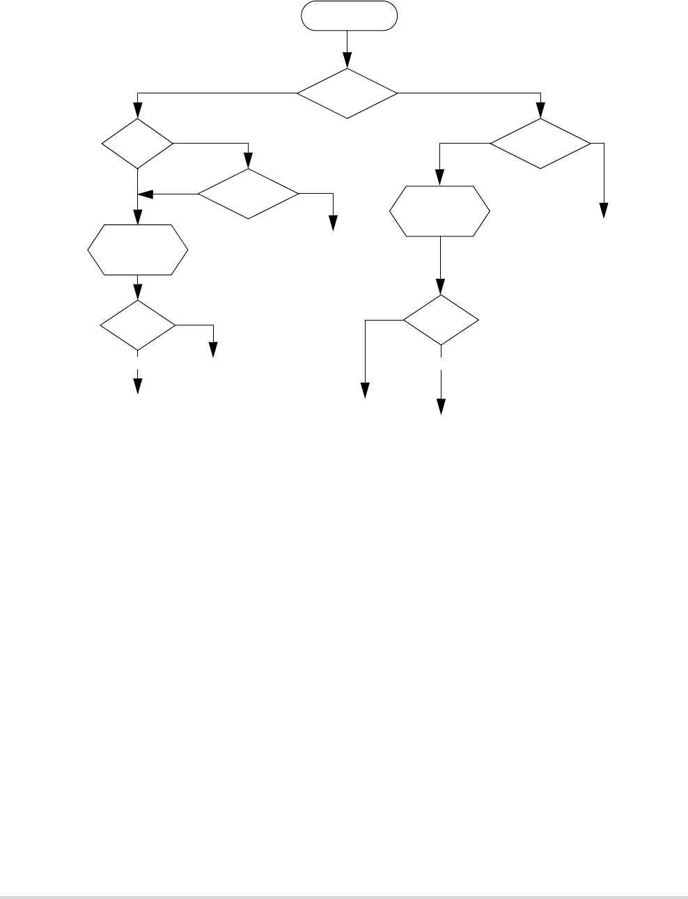
MOTOROLA Chapter 17. Fast Ethernet Controller (FEC) 17-13
Functional Description
Figure 17-3. Ethernet Address Recognitionq—Microcode Decisions
17.4.9 Hash Algorithm
The hash table algorithm used in the group and individual hash filtering operates as follows.
The 48-bit destination address is mapped into one of 64 bits, which are represented by 64
bits stored in GAUR, GALR (group address hash match) or IAUR, IALR (individual
address hash match). This mapping is performed by passing the 48-bit address through the
on-chip 32-bit CRC generator and selecting the 6 most significant bits of the CRC-encoded
result to generate a number between 0 and 63. The MSB of the CRC result selects GAUR
(MSB = 1) or GALR (MSB = 0). The least significant 5 bits of the hash result select the bit
within the selected register. If the CRC generator selects a bit that is set in the hash table,
the frame is accepted; otherwise, it is rejected.
For example, if eight group addresses are stored in the hash table and random group
addresses are received, the hash table prevents roughly 56/64 (or 87.5%) of the group
address frames from reaching memory. Those that do reach memory must be further filtered
by the processor to determine if they truly contain one of the eight desired addresses.
Receive Address
I/G Address
?
Exact Match
?
Hash Search
Group Table
Match
?
Hash Search
Individual Table
False
Match
?
False False
True True
True
NOTES:
FCE - field in RCR register (Flow Control Enable)
I/G - Individual/Group bit in Destination Address (least significant bit in first byte received in MAC frame)
Individual
Group
True
False
True
False
?
Pause Address
FCE
?
Recognition
Reject Frame
Flush from FIFO
Reject Frame
Flush from FIFO Receive Frame
Receive Frame
Receive Frame
Receive Frame

17-14 MCF5282 User’s Manual MOTOROLA
Functional Description
The effectiveness of the hash table declines as the number of addresses increases.
The hash table registers must be initialized by the user. The CRC32 polynomial to use in
computing the hash is:
A table of example Destination Addresses and corresponding hash values is included below
for reference.
Table 17-7. Destination Address to 6-Bit Hash
48-bit DA 6-bit Hash (in
hex)
Hash Decimal
Value
65:ff:ff:ff:ff:ff 0x0 0
55:ff:ff:ff:ff:ff 0x1 1
15:ff:ff:ff:ff:ff 0x2 2
35:ff:ff:ff:ff:ff 0x3 3
b5:ff:ff:ff:ff:ff 0x4 4
95:ff:ff:ff:ff:ff 0x5 5
d5:ff:ff:ff:ff:ff 0x6 6
f5:ff:ff:ff:ff:ff 0x7 7
db:ff:ff:ff:ff:ff 0x8 8
fb:ff:ff:ff:ff:ff 0x9 9
bb:ff:ff:ff:ff:ff 0xa 10
8b:ff:ff:ff:ff:ff 0xb 11
0b:ff:ff:ff:ff:ff 0xc 12
3b:ff:ff:ff:ff:ff 0xd 13
7b:ff:ff:ff:ff:ff 0xe 14
5b:ff:ff:ff:ff:ff 0xf 15
27:ff:ff:ff:ff:ff 0x10 16
07:ff:ff:ff:ff:ff 0x11 17
57:ff:ff:ff:ff:ff 0x12 18
77:ff:ff:ff:ff:ff 0x13 19
f7:ff:ff:ff:ff:ff 0x14 20
c7:ff:ff:ff:ff:ff 0x15 21
97:ff:ff:ff:ff:ff 0x16 22
a7:ff:ff:ff:ff:ff 0x17 23
X32 X26 X23 X22 X16 X12 X11 X10 X8X7X5X4X2X1++++++++++++++

MOTOROLA Chapter 17. Fast Ethernet Controller (FEC) 17-15
Functional Description
99:ff:ff:ff:ff:ff 0x18 24
b9:ff:ff:ff:ff:ff 0x19 25
f9:ff:ff:ff:ff:ff 0x1a 26
c9:ff:ff:ff:ff:ff 0x1b 27
59:ff:ff:ff:ff:ff 0x1c 28
79:ff:ff:ff:ff:ff 0x1d 29
29:ff:ff:ff:ff:ff 0x1e 30
19:ff:ff:ff:ff:ff 0x1f 31
d1:ff:ff:ff:ff:ff 0x20 32
f1:ff:ff:ff:ff:ff 0x21 33
b1:ff:ff:ff:ff:ff 0x22 34
91:ff:ff:ff:ff:ff 0x23 35
11:ff:ff:ff:ff:ff 0x24 36
31:ff:ff:ff:ff:ff 0x25 37
71:ff:ff:ff:ff:ff 0x26 38
51:ff:ff:ff:ff:ff 0x27 39
7f:ff:ff:ff:ff:ff 0x28 40
4f:ff:ff:ff:ff:ff 0x29 41
1f:ff:ff:ff:ff:ff 0x2a 42
3f:ff:ff:ff:ff:ff 0x2b 43
bf:ff:ff:ff:ff:ff 0x2c 44
9f:ff:ff:ff:ff:ff 0x2d 45
df:ff:ff:ff:ff:ff 0x2e 46
ef:ff:ff:ff:ff:ff 0x2f 47
93:ff:ff:ff:ff:ff 0x30 48
b3:ff:ff:ff:ff:ff 0x31 49
f3:ff:ff:ff:ff:ff 0x32 50
d3:ff:ff:ff:ff:ff 0x33 51
53:ff:ff:ff:ff:ff 0x34 52
73:ff:ff:ff:ff:ff 0x35 53
23:ff:ff:ff:ff:ff 0x36 54
13:ff:ff:ff:ff:ff 0x37 55
3d:ff:ff:ff:ff:ff 0x38 56
Table 17-7. Destination Address to 6-Bit Hash (continued)
48-bit DA 6-bit Hash (in
hex)
Hash Decimal
Value
17-16 MCF5282 User’s Manual MOTOROLA
Functional Description
17.4.10 Full Duplex Flow Control
Full-duplex flow control allows the user to transmit pause frames and to detect received
pause frames. Upon detection of a pause frame, MAC data frame transmission stops for a
given pause duration.
To enable pause frame detection, the FEC must operate in full-duplex mode (TCR[FDEN]
asserted) and flow control enable (RCR[FCE]) must be asserted. The FEC detects a pause
frame when the fields of the incoming frame match the pause frame specifications, as
shown in the table below. In addition, the receive status associated with the frame should
indicate that the frame is valid.
Pause frame detection is performed by the receiver and microcontroller modules. The
microcontroller runs an address recognition subroutine to detect the specified pause frame
destination address, while the receiver detects the type and opcode pause frame fields. On
detection of a pause frame, TCR[GTS] is asserted by the FEC internally. When
transmission has paused, the EIR[GRA] interrupt is asserted and the pause timer begins to
increment. Note that the pause timer makes use of the transmit backoff timer hardware,
which is used for tracking the appropriate collision backoff time in half-duplex mode. The
pause timer increments once every slot time, until OPD[PAUSE_DUR] slot times have
expired. On OPD[PAUSE_DUR] expiration, TCR[GTS] is deasserted allowing MAC data
frame transmission to resume. Note that the receive flow control pause
(TCR[RFC_PAUSE]) status bit is asserted while the transmitter is paused due to reception
of a pause frame.
0d:ff:ff:ff:ff:ff 0x39 57
5d:ff:ff:ff:ff:ff 0x3a 58
7d:ff:ff:ff:ff:ff 0x3b 59
fd:ff:ff:ff:ff:ff 0x3c 60
dd:ff:ff:ff:ff:ff 0x3d 61
9d:ff:ff:ff:ff:ff 0x3e 62
bd:ff:ff:ff:ff:ff 0x3f 63
Table 17-8. PAUSE Frame Field Specification
48-bit Destination Address 0x0180_c200_0001 or Physical Address
48-bit Source Address Any
16-bit Type 0x8808
16-bit Opcode 0x0001
16-bit PAUSE Duration 0x0000 to 0xFFFF
Table 17-7. Destination Address to 6-Bit Hash (continued)
48-bit DA 6-bit Hash (in
hex)
Hash Decimal
Value

MOTOROLA Chapter 17. Fast Ethernet Controller (FEC) 17-17
Functional Description
To transmit a pause frame, the FEC must operate in full-duplex mode and the user must
assert flow control pause (TCR[TFC_PAUSE]). On assertion of transmit flow control
pause (TCR[TFC_PAUSE]), the transmitter asserts TCR[GTS] internally. When the
transmission of data frames stops, the EIR[GRA] (graceful stop complete) interrupt asserts.
Following EIR[GRA] assertion, the pause frame is transmitted. On completion of pause
frame transmission, flow control pause (TCR[TFC_PAUSE]) and TCR[GTS] are
deasserted internally.
The user must specify the desired pause duration in the OPD register.
Note that when the transmitter is paused due to receiver/microcontroller pause frame
detection, transmit flow control pause (TCR[TFC_PAUSE]) still may be asserted and will
cause the transmission of a single pause frame. In this case, the EIR[GRA] interrupt will
not be asserted.
17.4.11 Inter-Packet Gap (IPG) Time
The minimum inter-packet gap time for back-to-back transmission is 96 bit times. After
completing a transmission or after the backoff algorithm completes, the transmitter waits
for carrier sense to be negated before starting its 96 bit time IPG counter. Frame
transmission may begin 96 bit times after carrier sense is negated if it stays negated for at
least 60 bit times. If carrier sense asserts during the last 36 bit times, it will be ignored and
a collision will occur.
The receiver receives back-to-back frames with a minimum spacing of at least 28 bit times.
If an inter-packet gap between receive frames is less than 28 bit times, the following frame
may be discarded by the receiver.
17.4.12 Collision Handling
If a collision occurs during frame transmission, the Ethernet controller will continue the
transmission for at least 32 bit times, transmitting a JAM pattern consisting of 32 ones. If
the collision occurs during the preamble sequence, the JAM pattern will be sent after the
end of the preamble sequence.
If a collision occurs within 512 bit times, the retry process is initiated. The transmitter waits
a random number of slot times. A slot time is 512 bit times. If a collision occurs after 512
bit times, then no retransmission is performed and the end of frame buffer is closed with a
Late Collision (LC) error indication.
17.4.13 Internal and External Loopback
Both internal and external loopback are supported by the Ethernet controller. In loopback
mode, both of the FIFOs are used and the FEC actually operates in a full-duplex fashion.

17-18 MCF5282 User’s Manual MOTOROLA
Functional Description
Both internal and external loopback are configured using combinations of the LOOP and
DRT bits in the RCR register and the FDEN bit in the TCR register.
For both internal and external loopback set FDEN = 1.
For internal loopback set RCR[LOOP] = 1 and RCR[DRT] = 0. ETXEN and ETXER will
not assert during internal loopback. During internal loopback, the transmit/receive data rate
is higher than in normal operation because the internal system clock is used by the transmit
and receive blocks instead of the clocks from the external transceiver. This will cause an
increase in the required system bus bandwidth for transmit and receive data being DMA’d
to/from external memory. It may be necessary to pace the frames on the transmit side and/or
limit the size of the frames to prevent transmit FIFO underrun and receive FIFO overflow.
For external loopback set RCR[LOOP] = 0, RCR[DRT] = 0 and configure the external
transceiver for loopback.
17.4.14 Ethernet Error-Handling Procedure
The Ethernet controller reports frame reception and transmission error conditions using the
FEC RxBDs, the EIR register, and the MIB block counters.
17.4.14.1 Transmission Errors
17.4.14.1.1 Transmitter Underrun
If this error occurs, the FEC sends 32 bits that ensure a CRC error and stops transmitting.
All remaining buffers for that frame are then flushed and closed. The UN bit is set in the
EIR. The FEC will then continue to the next transmit buffer descriptor and begin
transmitting the next frame.
The “UN” interrupt will be asserted if enabled in the EIMR register.
17.4.14.1.2 Retransmission Attempts Limit Expired
When this error occurs, the FEC terminates transmission. All remaining buffers for that
frame are flushed and closed, and the RL bit is set in the EIR. The FEC will then continue
to the next transmit buffer descriptor and begin transmitting the next frame.
The “RL” interrupt will be asserted if enabled in the EIMR register.
17.4.14.1.3 Late Collision
When a collision occurs after the slot time (512 bits starting at the Preamble), the FEC
terminates transmission. All remaining buffers for that frame are flushed and closed, and
the LC bit is set in the EIR register. The FEC will then continue to the next transmit buffer
descriptor and begin transmitting the next frame.
The “LC” interrupt will be asserted if enabled in the EIMR register.

MOTOROLA Chapter 17. Fast Ethernet Controller (FEC) 17-19
Functional Description
17.4.14.1.4 Heartbeat
Some transceivers have a self-test feature called “heartbeat” or “signal quality error.” To
signify a good self-test, the transceiver indicates a collision to the FEC within 4
microseconds after completion of a frame transmitted by the Ethernet controller. This
indication of a collision does not imply a real collision error on the network, but is rather
an indication that the transceiver still seems to be functioning properly. This is called the
heartbeat condition.
If the HBC bit is set in the TCR register and the heartbeat condition is not detected by the
FEC after a frame transmission, then a heartbeat error occurs. When this error occurs, the
FEC closes the buffer, sets the HB bit in the EIR register, and generates the HBERR
interrupt if it is enabled.
17.4.14.2 Reception Errors
17.4.14.2.1 Overrun Error
If the receive block has data to put into the receive FIFO and the receive FIFO is full, the
FEC sets the OV bit in the RxBD. All subsequent data in the frame will be discarded and
subsequent frames may also be discarded until the receive FIFO is serviced by the DMA
and space is made available. At this point the receive frame/status word is written into the
FIFO with the OV bit set. This frame must be discarded by the driver.
17.4.14.2.2 Non-Octet Error (Dribbling Bits)
The Ethernet controller handles up to seven dribbling bits when the receive frame
terminates past an non-octet aligned boundary. Dribbling bits are not used in the CRC
calculation. If there is a CRC error, then the frame non-octet aligned (NO) error is reported
in the RxBD. If there is no CRC error, then no error is reported.
17.4.14.2.3 CRC Error
When a CRC error occurs with no dribble bits, the FEC closes the buffer and sets the CR
bit in the RxBD. CRC checking cannot be disabled, but the CRC error can be ignored if
checking is not required.
17.4.14.2.4 Frame Length Violation
When the receive frame length exceeds MAX_FL bytes the BABR interrupt will be
generated, and the LG bit in the end of frame RxBD will be set. The frame is not truncated
unless the frame length exceeds 2047 bytes).
17-20 MCF5282 User’s Manual MOTOROLA
Programming Model
17.4.14.2.5 Truncation
When the receive frame length exceeds 2047 bytes the frame is truncated and the TR bit is
set in the receive BD.
17.5 Programming Model
This section gives an overview of the registers, followed by a description of the buffers.
The FEC is programmed by a combination of control/status registers (CSRs) and buffer
descriptors. The CSRs are used for mode control and to extract global status information.
The descriptors are used to pass data buffers and related buffer information between the
hardware and software.
17.5.1 Top Level Module Memory Map
The FEC implementation requires a 1-Kbyte memory map space. This is divided into 2
sections of 512 bytes each. The first is used for control/status registers. The second contains
event/statistic counters held in the MIB block. Table 17-9 defines the top level memory
map.
17.5.2 Detailed Memory Map (Control/Status Registers)
Table 17-10 shows the FEC register memory map with each register address, name, and a
brief description.
Table 17-9. Module Memory Map
Address Function
IPSBAR + 0x1000-11FF Control/Status Registers
IPSBAR + 0x1200-13FF MIB Block Counters
Table 17-10. FEC Register Memory Map
IPSBAR
Offset Name Width Description
0x1004 EIR 32 Interrupt Event Register
0x1008 EIMR 32 Interrupt Mask Register
0x1010 RDAR 32 Receive Descriptor Active Register
0x1014 TDAR 32 Transmit Descriptor Active Register
0x1024 ECR 32 Ethernet Control Register
0x1040 MDATA 32 MII Data Register
0x1044 MSCR 32 MII Speed Control Register
0x1064 MIBC 32 MIB Control/Status Register

MOTOROLA Chapter 17. Fast Ethernet Controller (FEC) 17-21
Programming Model
17.5.3 MIB Block Counters Memory Map
Table 17-11 defines the MIB Counters memory map which defines the locations in the MIB
RAM space where hardware maintained counters reside. These fall in the 0x1200-0x13FF
address offset range. The counters are divided into two groups.
RMON counters are included which cover the Ethernet Statistics counters defined in RFC
1757. In addition to the counters defined in the Ethernet Statistics group, a counter is
included to count truncated frames as the FEC only supports frame lengths up to 2047
bytes. The RMON counters are implemented independently for transmit and receive to
insure accurate network statistics when operating in full duplex mode.
IEEE counters are included which support the Mandatory and Recommended counter
packages defined in section 5 of ANSI/IEEE Std. 802.3 (1998 edition). The IEEE Basic
Package objects are supported by the FEC but do not require counters in the MIB block. In
addition, some of the recommended package objects which are supported do not require
MIB counters. Counters for transmit and receive full duplex flow control frames are
included as well.
0x1084 RCR 32 Receive Control Register
0x10C4 TCR 32 Transmit Control Register
0x10E4 PALR 32 Physical Address Low Register
0x10E8 PAUR 32 Physical Address High+ Type Field
0x10EC OPD 32 Opcode + Pause Duration
0x1118 IAUR 32 Upper 32 bits of Individual Hash Table
0x111C IALR 32 Lower 32 Bits of Individual Hash Table
0x1120 GAUR 32 Upper 32 bits of Group Hash Table
0x1124 GALR 32 Lower 32 bits of Group Hash Table
0x1144 TFWR 32 Transmit FIFO Watermark
0x114C FRBR 32 FIFO Receive Bound Register
0x1150 FRSR 32 FIFO Receive FIFO Start Registers
0x1180 ERDSR 32 Pointer to Receive Descriptor Ring
0x1184 ETDSR 32 Pointer to Transmit Descriptor Ring
0x1188 EMRBR 32 Maximum Receive Buffer Size
Table 17-10. FEC Register Memory Map (continued)
IPSBAR
Offset Name Width Description

17-22 MCF5282 User’s Manual MOTOROLA
Programming Model
Table 17-11. MIB Counters Memory Map
IPSBAR
Offset Mnemonic Description
0x1200 RMON_T_DROP Count of frames not counted correctly
0x1204 RMON_T_PACKETS RMON Tx packet count
0x1208 RMON_T_BC_PKT RMON Tx Broadcast Packets
0x120C RMON_T_MC_PKT RMON Tx Multicast Packets
0x1210 RMON_T_CRC_ALIGN RMON Tx Packets w CRC/Align error
0x1214 RMON_T_UNDERSIZE RMON Tx Packets < 64 bytes, good crc
0x1218 RMON_T_OVERSIZE RMON Tx Packets > MAX_FL bytes, good crc
0x121C RMON_T_FRAG RMON Tx Packets < 64 bytes, bad crc
0x1220 RMON_T_JAB RMON Tx Packets > MAX_FL bytes, bad crc
0x1224 RMON_T_COL RMON Tx collision count
0x1228 RMON_T_P64 RMON Tx 64 byte packets
0x122C RMON_T_P65TO127 RMON Tx 65 to 127 byte packets
0x1230 RMON_T_P128TO255 RMON Tx 128 to 255 byte packets
0x1234 RMON_T_P256TO511 RMON Tx 256 to 511 byte packets
0x1238 RMON_T_P512TO1023 RMON Tx 512 to 1023 byte packets
0x123C RMON_T_P1024TO2047 RMON Tx 1024 to 2047 byte packets
0x1240 RMON_T_P_GTE2048 RMON Tx packets w > 2048 bytes
0x1244 RMON_T_OCTETS RMON Tx Octets
0x1248 IEEE_T_DROP Count of frames not counted correctly
0x124C IEEE_T_FRAME_OK Frames Transmitted OK
0x1250 IEEE_T_1COL Frames Transmitted with Single Collision
0x1254 IEEE_T_MCOL Frames Transmitted with Multiple Collisions
0x1258 IEEE_T_DEF Frames Transmitted after Deferral Delay
0x125c IEEE_T_LCOL Frames Transmitted with Late Collision
0x1260 IEEE_T_EXCOL Frames Transmitted with Excessive Collisions
0x1264 IEEE_T_MACERR Frames Transmitted with Tx FIFO Underrun
0x1268 IEEE_T_CSERR Frames Transmitted with Carrier Sense Error
0x126C IEEE_T_SQE Frames Transmitted with SQE Error
0x1270 IEEE_T_FDXFC Flow Control Pause frames transmitted
0x1274 IEEE_T_OCTETS_OK Octet count for Frames Transmitted w/o Error
0x1284 RMON_R_PACKETS RMON Rx packet count
0x1288 RMON_R_BC_PKT RMON Rx Broadcast Packets
0x128C RMON_R_MC_PKT RMON Rx Multicast Packets

MOTOROLA Chapter 17. Fast Ethernet Controller (FEC) 17-23
Programming Model
17.5.4 Registers
The following sections describe each register in detail.
17.5.4.1 Ethernet Interrupt Event Register (EIR)
When an event occurs that sets a bit in the EIR, an interrupt will be generated if the
corresponding bit in the interrupt mask register (EIMR) is also set. The bit in the EIR is
cleared if a one is written to that bit position; writing zero has no effect. This register is
cleared upon hardware reset.
These interrupts can be divided into operational interrupts, transceiver/network error
interrupts, and internal error interrupts. Interrupts which may occur in normal operation are
GRA, TXF, TXB, RXF, RXB, and MII. Interrupts resulting from errors/problems detected
0x1290 RMON_R_CRC_ALIGN RMON Rx Packets w CRC/Align error
0x1294 RMON_R_UNDERSIZE RMON Rx Packets < 64 bytes, good crc
0x1298 RMON_R_OVERSIZE RMON Rx Packets > MAX_FL bytes, good crc
0x129C RMON_R_FRAG RMON Rx Packets < 64 bytes, bad crc
0x12A0 RMON_R_JAB RMON Rx Packets > MAX_FL bytes, bad crc
0x12A4 RMON_R_RESVD_0
0x12A8 RMON_R_P64 RMON Rx 64 byte packets
0x12AC RMON_R_P65TO127 RMON Rx 65 to 127 byte packets
0x12B0 RMON_R_P128TO255 RMON Rx 128 to 255 byte packets
0x12B4 RMON_R_P256TO511 RMON Rx 256 to 511 byte packets
0x12B8 RMON_R_P512TO1023 RMON Rx 512 to 1023 byte packets
0x12BC RMON_R_P1024TO2047 RMON Rx 1024 to 2047 byte packets
0x12C0 RMON_R_P_GTE2048 RMON Rx packets w > 2048 bytes
0x12C4 RMON_R_OCTETS RMON Rx Octets
0x12C8 IEEE_R_DROP Count of frames not counted correctly
0x12CC IEEE_R_FRAME_OK Frames Received OK
0x12D0 IEEE_R_CRC Frames Received with CRC Error
0x12D4 IEEE_R_ALIGN Frames Received with Alignment Error
0x12D8 IEEE_R_MACERR Receive Fifo Overflow count
0x12DC IEEE_R_FDXFC Flow Control Pause frames received
0x12E0 IEEE_R_OCTETS_OK Octet count for Frames Rcvd w/o Error
Table 17-11. MIB Counters Memory Map (continued)
IPSBAR
Offset Mnemonic Description

17-24 MCF5282 User’s Manual MOTOROLA
Programming Model
in the network or transceiver are HBERR, BABR, BABT, LC and RL. Interrupts resulting
from internal errors are HBERR and UN.
Some of the error interrupts are independently counted in the MIB block counters. Software
may choose to mask off these interrupts since these errors will be visible to network
management via the MIB counters.
• HBERR - IEEE_T_SQE
• BABR - RMON_R_OVERSIZE (good CRC), RMON_R_JAB (bad CRC)
• BABT - RMON_T_OVERSIZE (good CRC), RMON_T_JAB (bad CRC)
• LATE_COL - IEEE_T_LCOL
• COL_RETRY_LIM - IEEE_T_EXCOL
• XFIFO_UN - IEEE_T_MACERR
31 30 29 28 27 26 25 24 23 22 21 20 19 18 16
Field HBERR BABR BABT GRA TXF TXB RXF RXB MII EBERR LC RL UN —
Reset 0000_0000_0000_0000
R/W R/W
15 0
Field —
Reset 0000_0000_0000_0000
R/W R/W
Address IPSBAR + 0x1004
Figure 17-4. Ethernet Interrupt Event Register (EIR)
Table 17-12. EIR Field Descriptions
Bits Name Description
31 HBERR Heartbeat error. This interrupt indicates that HBC is set in the TCR
register and that the COL input was not asserted within the
Heartbeat window following a transmission.
30 BABR Babbling receive error. This bit indicates a frame was received with
length in excess of RCR[MAX_FL] bytes.
29 BABT Babbling transmit error. This bit indicates that the transmitted
frame length has exceeded RCR[MAX_FL] bytes. This condition is
usually caused by a frame that is too long being placed into the
transmit data buffer(s). Truncation does not occur.

MOTOROLA Chapter 17. Fast Ethernet Controller (FEC) 17-25
Programming Model
28 GRA Graceful stop complete. This interrupt will be asserted for one of
three reasons. Graceful stop means that the transmitter is put into
a pause state after completion of the frame currently being
transmitted.
1) A graceful stop, which was initiated by the setting of the
TCR[GTS] bit is now complete.
2) A graceful stop, which was initiated by the setting of the
TCR[TFC_PAUSE] bit is now complete.
3) A graceful stop, which was initiated by the reception of a valid
full duplex flow control “pause” frame is now complete. Refer to
the “Full Duplex Flow Control” section of the Functional
Description chapter.
27 TXF Transmit frame interrupt. This bit indicates that a frame has been
transmitted and that the last corresponding buffer descriptor has
been updated.
26 TXB Transmit buffer interrupt. This bit indicates that a transmit buffer
descriptor has been updated.
25 RXF Receive frame interrupt. This bit indicates that a frame has been
received and that the last corresponding buffer descriptor has been
updated.
24 RXB Receive buffer interrupt. This bit indicates that a receive buffer
descriptor has been updated that was not the last in the frame.
23 MII MII interrupt. This bit indicates that the MII has completed the data
transfer requested.
22 EBERR Ethernet bus error. This bit indicates that a system bus error
occurred when a DMA transaction was underway. When the
EBERR bit is set, ECR[ETHER_EN] will be cleared, halting frame
processing by the FEC. When this occurs software will need to
insure that the FIFO controller and DMA are also soft reset.
21 LC Late collison. This bit indicates that a collision occurred beyond the
collision window (slot time) in half duplex mode. The frame is
truncated with a bad CRC and the remainder of the frame is
discarded.
20 RL Collision retry limit. This bit indicates that a collision occurred on
each of 16 successive attempts to transmit the frame. The frame is
discarded without being transmitted and transmission of the next
frame will commence. Can only occur in half duplex mode.
19 UN Transmit FIFO underrun. This bit indicates that the transmit FIFO
became empty before the complete frame was transmitted. A bad
CRC is appended to the frame fragment and the remainder of the
frame is discarded.
18–0 — Reserved, should be cleared.
Table 17-12. EIR Field Descriptions (continued)
Bits Name Description

17-26 MCF5282 User’s Manual MOTOROLA
Programming Model
17.5.4.2 Interrupt Mask Register (EIMR)
The EIMR register controls which interrupt events are allowed to generate actual interrupts.
All implemented bits in this CSR are read/write. This register is cleared upon a hardware
reset. If the corresponding bits in both the EIR and EIMR registers are set, the interrupt will
be signalled to the CPU. The interrupt signal will remain asserted until a 1 is written to the
EIR bit (write 1 to clear) or a 0 is written to the EIMR bit.
17.5.4.3 Receive Descriptor Active Register (RDAR)
RDAR is a command register, written by the user, that indicates that the receive descriptor
ring has been updated (empty receive buffers have been produced by the driver with the
empty bit set).
Whenever the register is written, the RDAR bit is set. This is independent of the data
actually written by the user. When set, the FEC will poll the receive descriptor ring and
process receive frames (provided ECR[ETHER_EN] is also set). Once the FEC polls a
receive descriptor whose empty bit is not set, then the FEC will clear the RDAR bit and
cease receive descriptor ring polling until the user sets the bit again, signifying that
additional descriptors have been placed into the receive descriptor ring.
31 30 29 28 27 26 25 24 23 22 21 20 19 18 16
Field HBERR BABR BABT GRA TXF TXB RXF RXB MII EBERR LC RL UN —
Reset 0000_0000_0000_0000
R/W R/W
15 0
Field —
Reset 0000_0000_0000_0000
R/W R/W
Address IPSBAR + 0x1008
Figure 17-5. Interrupt Mask Register (EIMR)
Table 17-13. EIMR Field Descriptions
Bits Name Description
31–19 See Figure 17-5
and Table 17-12.
Interrupt mask. Each bit corresponds to an interrupt source defined
by the EIR register. The corresponding EIMR bit determines
whether an interrupt condition can generate an interrupt. At every
processor clock, the EIR samples the signal generated by the
interrupting source. The corresponding EIR bit reflects the state of
the interrupt signal even if the corresponding EIMR bit is set.
0 The corresponding interrupt source is masked.
1 The corresponding interrupt source is not masked.
18–0 — Reserved, should be cleared.

MOTOROLA Chapter 17. Fast Ethernet Controller (FEC) 17-27
Programming Model
The RDAR register is cleared at reset and when ECR[ETHER_EN] is cleared.
17.5.4.4 Transmit Descriptor Active Register (TDAR)
The TDAR is a command register which should be written by the user to indicate that the
transmit descriptor ring has been updated (transmit buffers have been produced by the
driver with the ready bit set in the buffer descriptor).
Whenever the register is written, the TDAR bit is set. This value is independent of the data
actually written by the user. When set, the FEC will poll the transmit descriptor ring and
process transmit frames (provided ECR[ETHER_EN] is also set). Once the FEC polls a
transmit descriptor whose ready bit is not set, then the FEC will clear the TDAR bit and
cease transmit descriptor ring polling until the user sets the bit again, signifying additional
descriptors have been placed into the transmit descriptor ring.
The TDAR register is cleared at reset, when ECR[ETHER_EN] is cleared, or when
ECR[RESET] is set.
31 25 24 23 16
Field — R_DES_ACTIVE —
Reset 0000_0000_0000_0000
R/W R/W
15 0
Field —
Reset 0000_0000_0000_0000
R/W R/W
Address IPSBAR + 0x1010
Figure 17-6. Receive Descriptor Active Register (RDAR)
Table 17-14. RDAR Field Descriptions
Bits Name Description
31–25 — Reserved, should be cleared.
24 R_DES_ACTIVE Set to one when this register is written, regardless of the value written.
Cleared by the FEC device whenever no additional “empty” descriptors
remain in the receive ring. Also cleared when ECR[ETHER_EN] is cleared.
23–0 — Reserved, should be cleared.

17-28 MCF5282 User’s Manual MOTOROLA
Programming Model
17.5.4.5 Ethernet Control Register (ECR)
ECR is a read/write user register, though both fields in this register may be altered by
hardware as well. The ECR is used to enable/disable the FEC.
31 25 24 23 16
Field — X_DES_ACTIVE —
Reset 0000_0000_0000_0000
R/W R/W
15 0
Field —
Reset 0000_0000_0000_0000
R/W R/W
Address IPSBAR + 0x1014
Figure 17-7. Transmit Descriptor Active Register (TDAR)
Table 17-15. TDAR Field Descriptions
Bits Name Description
31–25 — Reserved, should be cleared.
24 X_DES_ACTIVE Set to one when this register is written, regardless of the value written.
Cleared by the FEC device whenever no additional “ready” descriptors
remain in the transmit ring. Also cleared when ECR[ETHER_EN] is
cleared.
23–0 — Reserved, should be cleared.
31 16
Field —
Reset 1111_0000_0000_0000
R/W R/W
15 10
Field — ETHER_EN RESET
Reset 0000_0000_0000_0000
R/W R/W
Address IPSBAR + 0x1024
Figure 17-8. Ethernet Control Register (ECR)

MOTOROLA Chapter 17. Fast Ethernet Controller (FEC) 17-29
Programming Model
17.5.4.6 MII Management Frame Register (MMFR)
The MMFR is accessed by the user and does not reset to a defined value. The MMFR
register is used to communicate with the attached MII compatible PHY device(s),
providing read/write access to their MII registers. Performing a write to the MMFR will
cause a management frame to be sourced unless the MSCR has been programmed to 0. In
the case of writing to MMFR when MSCR = 0, if the MSCR register is then written to a
non-zero value, an MII frame will be generated with the data previously written to the
MMFR. This allows MMFR and MSCR to be programmed in either order if MSCR is
currently zero.
Table 17-16. ECR Field Descriptions
Bits Name Description
31-2 — Reserved.
1 ETHER_EN When this bit is set, the FEC is enabled, and reception and
transmission are possible. When this bit is cleared, reception is
immediately stopped and transmission is stopped after a bad CRC
is appended to any currently transmitted frame. The buffer
descriptor(s) for an aborted transmit frame are not updated after
clearing this bit. When ETHER_EN is deasserted, the DMA, buffer
descriptor, and FIFO control logic are reset, including the buffer
descriptor and FIFO pointers. The ETHER_EN bit is altered by
hardware under the following conditions:
• ECR[RESET] is set by software, in which case ETHER_EN will
be cleared
• An error condition causes the EIR[EBERR] bit to set, in which
case ETHER_EN will be cleared
0 RESET When this bit is set, the equivalent of a hardware reset is
performed but it is local to the FEC. ETHER_EN is cleared and all
other FEC registers take their reset values. Also, any
transmission/reception currently in progress is abruptly aborted.
This bit is automatically cleared by hardware during the reset
sequence. The reset sequence takes approximately 8 system
clock cycles after RESET is written with a 1.
31 30 29 28 27 23 22 18 17 16
Field ST OP PA RA TA
Reset Undefined
R/W R/W
15 0
Field DATA
Reset Undefined
R/W R/W
Address IPSBAR + 0x1040
Figure 17-9. MII Management Frame Register (MMFR)

17-30 MCF5282 User’s Manual MOTOROLA
Programming Model
To perform a read or write operation on the MII Management Interface, the MMFR register
must be written by the user. To generate a valid read or write management frame, the ST
field must be written with a 01 pattern, and the TA field must be written with a 10. If other
patterns are written to these fields, a frame will be generated but will not comply with the
IEEE 802.3 MII definition.
To generate an IEEE 802.3-compliant MII Management Interface write frame (write to a
PHY register), the user must write {01 01 PHYAD REGAD 10 DATA} to the MMFR
register. Writing this pattern will cause the control logic to shift out the data in the MMFR
register following a preamble generated by the control state machine. During this time the
contents of the MMFR register will be altered as the contents are serially shifted and will
be unpredictable if read by the user. Once the write management frame operation has
completed, the MII interrupt will be generated. At this time the contents of the MMFR
register will match the original value written.
To generate an MII Management Interface read frame (read a PHY register) the user must
write {01 10 PHYAD REGAD 10 XXXX} to the MMFR register (the content of the DATA
field is a don’t care). Writing this pattern will cause the control logic to shift out the data in
the MMFR register following a preamble generated by the control state machine. During
this time the contents of the MMFR register will be altered as the contents are serially
shifted, and will be unpredictable if read by the user. Once the read management frame
operation has completed, the MII interrupt will be generated. At this time the contents of
the MMFR register will match the original value written except for the DATA field whose
contents have been replaced by the value read from the PHY register.
Table 17-17. MMFR Field Descriptions
Bit Name Description
31–30 ST Start of frame delimiter. These bits must be programmed to 01
for a valid MII management frame.
29–28 OP Operation code. This field must be programmed to 10 (read) or
01 (write) to generate a valid MII management frame. A value
of 11 will produce “read” frame operation while a value of 00 will
produce “write” frame operation, but these frames will not be MII
compliant.
27–23 PA PHY address. This field specifies one of up to 32 attached PHY
devices.
22–18 RA Register address. This field specifies one of up to 32 registers
within the specified PHY device.
17–16 TA Turn around. This field must be programmed to 10 to generate
a valid MII management frame.
15–0 DATA Management frame data. This is the field for data to be written
to or read from the PHY register.

MOTOROLA Chapter 17. Fast Ethernet Controller (FEC) 17-31
Programming Model
If the MMFR register is written while frame generation is in progress, the frame contents
will be altered. Software should use the MII_STATUS register and/or the MII interrupt to
avoid writing to the MMFR register while frame generation is in progress.
17.5.4.7 MII Speed Control Register (MSCR)
The MSCR provides control of the MII clock (EMDC pin) frequency, allows a preamble
drop on the MII management frame, and provides observability (intended for
manufacturing test) of an internal counter used in generating the EMDC clock signal.
The MII_SPEED field must be programmed with a value to provide an EMDC frequency
of less than or equal to 2.5 MHz to be compliant with the IEEE 802.3 MII specification.
The MII_SPEED must be set to a non-zero value in order to source a read or write
management frame. After the management frame is complete the MSCR register may
optionally be set to zero to turn off the EMDC. The EMDC generated will have a 50% duty
cycle except when MII_SPEED is changed during operation (change will take effect
following either a rising or falling edge of EMDC).
31 16
Field —
Reset 0000_0000_0000_0000
R/W R/W
15 8 7 6 1 0
Field — DIS_PREAMBLE MII_SPEED —
Reset 0000_0000_0000_0000
R/W R/W
Address IPSBAR + 0x1044
Figure 17-10. MII Speed Control Register (MSCR)
Table 17-18. MSCR Field Descriptions
Bits Name Description
31–8 — Reserved, should be cleared.
7 DIS_PREAMBLE Asserting this bit will cause preamble (32 1’s) not to be prepended
to the MII management frame. The MII standard allows the preamble
to be dropped if the attached PHY device(s) does not require it.
6–1 MII_SPEED MII_SPEED controls the frequency of the MII management interface
clock (EMDC) relative to the system clock. A value of 0 in this field
will “turn off” the EMDC and leave it in low voltage state. Any
non-zero value will result in the EMDC frequency of
1/(MII_SPEED*2) of the system clock frequency.
0 — Reserved, should be cleared.
17-32 MCF5282 User’s Manual MOTOROLA
Programming Model
If the system clock is 25 MHz, programming this register to 0x0000_0005 will result in an
EMDC frequency of 25 MHz * 1/10 = 2.5 MHz. A table showing optimum values for
MII_SPEED as a function of system clock frequency is provided below.
17.5.4.8 MIB Control Register (MIBC)
The MIBC is a read/write register used to provide control of and to observe the state of the
MIB block. This register is accessed by user software if there is a need to disable the MIB
block operation. For example, in order to clear all MIB counters in RAM the user should
disable the MIB block, then clear all the MIB RAM locations, then enable the MIB block.
The MIB_DISABLE bit is reset to 1. See Table 17-11 for the locations of the MIB counters.
Table 17-19. Programming Examples for MSCR
System Clock Frequency MII_SPEED (field in reg) EMDC frequency
25 MHz 0x5 2.5 MHz
33 MHz 0x7 2.36 MHz
40 MHz 0x8 2.5 MHz
50 MHz 0xA 2.5 MHz
66 MHz 0xD 2.5 MHz
31 30 16
Field MIB_DISABLE MIB_IDLE —
Reset 1100_0000_000_000
R/W R/W
15 0
Field —
Reset 0000_0000_0000_0000
R/W R/W
Address IPSBAR + 0x1064
Figure 17-11. MIB Control Register (MIBC)
Table 17-20. MIBC Field Descriptions
Bits Name Description
31 MIB_DISABLE A read/write control bit. If set, the MIB logic will halt and not update
any MIB counters.
30 MIB_IDLE A read-only status bit. If set the MIB block is not currently updating
any MIB counters.
29–0 — Reserved.

MOTOROLA Chapter 17. Fast Ethernet Controller (FEC) 17-33
Programming Model
17.5.4.9 Receive Control Register (RCR)
The RCR is programmed by the user. The RCR controls the operational mode of the receive
block and should be written only when ECR[ETHER_EN] = 0 (initialization time).
31 27 26 16
Field — MAX_FL
Reset 0000_0101_1110_1110
R/W R/W
15 6 5 4 3 2 1 0
Field — FCE BC_REJ PROM MII_MODE DRT LOOP
Reset 0000_0000_0000_0001
R/W R/W
Address IPSBAR + 0x1084
Figure 17-12. Receive Control Register (RCR)
Table 17-21. RCR Field Descriptions
Bits Name Description
31–27 — Reserved, should be cleared.
26–16 MAX_FL Maximum frame length. Resets to decimal 1518. Length is
measured starting at DA and includes the CRC at the end of
the frame. Transmit frames longer than MAX_FL will cause
the BABT interrupt to occur. Receive Frames longer than
MAX_FL will cause the BABR interrupt to occur and will set
the LG bit in the end of frame receive buffer descriptor. The
recommended default value to be programmed by the user is
1518 or 1522 (if VLAN Tags are supported).
15–6 — Reserved, should be cleared.
5 FCE Flow control enable. If asserted, the receiver will detect
PAUSE frames. Upon PAUSE frame detection, the
transmitter will stop transmitting data frames for a given
duration.
4 BC_REJ Broadcast frame reject. If asserted, frames with DA
(destination address) = FF_FF_FF_FF_FF_FF will be
rejected unless the PROM bit is set. If both BC_REJ and
PROM = 1, then frames with broadcast DA will be accepted
and the M (MISS) bit will be set in the receive buffer
descriptor.
3 PROM Promiscuous mode. All frames are accepted regardless of
address matching.
2 MII_MODE Media independent interface mode. Selects external
interface mode. Setting this bit to one selects MII mode,
setting this bit equal to zero selects 7-wire mode (used only
for serial 10 Mbps). This bit controls the interface mode for
both transmit and receive blocks.

17-34 MCF5282 User’s Manual MOTOROLA
Programming Model
17.5.4.10 Transmit Control Register (TCR)
The TCR is read/write and is written by the user to configure the transmit block. This
register is cleared at system reset. Bits 2 and 1 should be modified only when
ECR[ETHER_EN] = 0.
1 DRT Disable receive on transmit.
0 Receive path operates independently of transmit (use for
full duplex or to monitor transmit activity in half duplex
mode).
1 Disable reception of frames while transmitting (normally
used for half duplex mode).
0 LOOP Internal loopback. If set, transmitted frames are looped back
internal to the device and the transmit output signals are not
asserted. The system clock is substituted for the ETXCLK
when LOOP is asserted. DRT must be set to zero when
asserting LOOP.
31 16
Field —
Reset 0000_0000_0000_0000
R/W R/W
15 5 4 3 2 1 0
Field — RFC_PAUSE TFC_PAUSE FDEN HBC GTS
Reset 0000_0000_0000_0000
R/W R/W R R/W
Address IPSBAR + 0x10C4
Figure 17-13. Transmit Control Register (TCR)
Table 17-21. RCR Field Descriptions (continued)
Bits Name Description

MOTOROLA Chapter 17. Fast Ethernet Controller (FEC) 17-35
Programming Model
17.5.4.11 Physical Address Low Register (PALR)
The PALR is written by the user. This register contains the lower 32 bits (bytes 0,1,2,3) of
the 48-bit address used in the address recognition process to compare with the DA
(Destination Address) field of receive frames with an individual DA. In addition, this
register is used in bytes 0 through 3 of the 6-byte source address field when transmitting
PAUSE frames. This register is not reset and must be initialized by the user.
Table 17-22. TCR Field Descriptions
Bits Name Description
31–5 — Reserved, should be cleared.
4 RFC_PAUSE Receive frame control pause. This read-only status bit will be
asserted when a full duplex flow control pause frame has been
received and the transmitter is paused for the duration defined in
this pause frame. This bit will automatically clear when the pause
duration is complete.
3 TFC_PAUSE Transmit frame control pause. Transmits a PAUSE frame when
asserted. When this bit is set, the MAC will stop transmission of
data frames after the current transmission is complete. At this
time, the GRA interrupt in the EIR register will be asserted. With
transmission of data frames stopped, the MAC will transmit a
MAC Control PAUSE frame. Next, the MAC will clear the
TFC_PAUSE bit and resume transmitting data frames. Note that
if the transmitter is paused due to user assertion of GTS or
reception of a PAUSE frame, the MAC may still transmit a MAC
Control PAUSE frame.
2 FDEN Full duplex enable. If set, frames are transmitted independent of
carrier sense and collision inputs. This bit should only be
modified when ETHER_EN is deasserted.
1 HBC Heartbeat control. If set, the heartbeat check is performed
following end of transmission and the HB bit in the status register
will be set if the collision input does not assert within the
heartbeat window. This bit should only be modified when
ETHER_EN is deasserted.
0 GTS Graceful transmit stop. When this bit is set, the MAC will stop
transmission after any frame that is currently being transmitted is
complete and the GRA interrupt in the EIR register will be
asserted. If frame transmission is not currently underway, the
GRA interrupt will be asserted immediately. Once transmission
has completed, a “restart” can be accomplished by clearing the
GTS bit. The next frame in the transmit FIFO will then be
transmitted. If an early collision occurs during transmission when
GTS = 1, transmission will stop after the collision. The frame will
be transmitted again once GTS is cleared. Note that there may
be old frames in the transmit FIFO that will be transmitted when
GTS is reasserted. To avoid this deassert ECR[ETHER_EN]
following the GRA interrupt.

17-36 MCF5282 User’s Manual MOTOROLA
Programming Model
17.5.4.12 Physical Address High Register (PAUR)
The PAUR is written by the user. This register contains the upper 16 bits (bytes 4 and 5) of
the 48-bit address used in the address recognition process to compare with the DA
(destination address) field of receive frames with an individual DA. In addition, this
register is used in bytes 4 and 5 of the 6-byte Source Address field when transmitting
PAUSE frames. Bits 15:0 of PAUR contain a constant type field (0x8808) used for
transmission of PAUSE frames. This register is not reset and bits 31:16 must be initialized
by the user.
31 16
Field PADDR1
Reset Uninitialized
R/W R/W
15 0
Field PADDR1
Reset Uninitialized
R/W R/W
Address IPSBAR + 0x10E4
Figure 17-14. Physical Address Low Register (PALR)
Table 17-23. PALR Field Descriptions
Bits Name Description
31–0 PADDR1 Bytes 0 (bits 31:24), 1 (bits 23:16), 2 (bits 15:8) and 3 (bits
7:0) of the 6-byte individual address to be used for exact
match, and the Source Address field in PAUSE frames.
31 16
Field PADDR2
Reset Uninitialized
R/W R/W
15 0
Field TYPE
Reset 1000_1000_0000_1000
R/W R
Address IPSBAR + 0x10E8
Figure 17-15. Physical Address High Register (PAUR)

MOTOROLA Chapter 17. Fast Ethernet Controller (FEC) 17-37
Programming Model
17.5.4.13 Opcode/Pause Duration Register (OPD)
The OPD is read/write accessible. This register contains the 16-bit opcode and 16-bit pause
duration fields used in transmission of a PAUSE frame. The opcode field is a constant
value, 0x0001. When another node detects a PAUSE frame, that node will pause
transmission for the duration specified in the pause duration field. This register is not reset
and must be initialized by the user.
17.5.4.14 Descriptor Individual Upper Address Register (IAUR)
The IAUR is written by the user. This register contains the upper 32 bits of the 64-bit
individual address hash table used in the address recognition process to check for possible
match with the DA field of receive frames with an individual DA. This register is not reset
and must be initialized by the user.
Table 17-24. PAUR Field Descriptions
BIts Name Description
31–16 PADDR2 Bytes 4 (bits 31:24) and 5 (bits 23:16) of the 6-byte individual
address to be used for exact match, and the Source Address
field in PAUSE frames.
15–0 TYPE Type field in PAUSE frames. These 16-bits are a constant
value of 0x8808.
31 16
Field OPCODE
Reset 0000_0000_0000_0001
R/W R
15 0
Field PAUSE_DUR
Reset Uninitialized
R/W R/W
Address IPSBAR + 0x10EC
Figure 17-16. Opcode/Pause Duration Register (OPD)
Table 17-25. OPD Field Descriptions
Bits Name Description
31–16 OPCODE Opcode field used in PAUSE frames.
These bits are a constant, 0x0001.
15–0 PAUSE_DUR Pause Duration field used in PAUSE frames.

17-38 MCF5282 User’s Manual MOTOROLA
Programming Model
17.5.4.15 Descriptor Individual Lower Address (IALR)
The IALR register is written by the user. This register contains the lower 32 bits of the
64-bit individual address hash table used in the address recognition process to check for
possible match with the DA field of receive frames with an individual DA. This register is
not reset and must be initialized by the user.
31 16
Field IADDR1
Reset Uninitialized
R/W R/W
15 0
Field IADDR1
Reset Uninitialized
R/W R/W
Address IPSBAR + 0x1118
Figure 17-17. Descriptor Individual Upper Address Register (IAUR)
Table 17-26. IAUR Field Descriptions
Bits Name Descriptions
31–0 IADDR1 The upper 32 bits of the 64-bit hash table used in the address
recognition process for receive frames with a unicast
address. Bit 31 of IADDR1 contains hash index bit 63. Bit 0
of IADDR1 contains hash index bit 32.
31 16
Field IADDR2
Reset Uninitialized
R/W R/W
15 0
Field IADDR2
Reset Uninitialized
R/W R/W
Address IPSBAR + 0x111C
Figure 17-18. Descriptor Individual Lower Address Register (IALR)

MOTOROLA Chapter 17. Fast Ethernet Controller (FEC) 17-39
Programming Model
17.5.4.16 Descriptor Group Upper Address (GAUR)
The GAUR is written by the user. This register contains the upper 32 bits of the 64-bit hash
table used in the address recognition process for receive frames with a multicast address.
This register must be initialized by the user.
17.5.4.17 Descriptor Group Lower Address (GALR)
The GALR register is written by the user. This register contains the lower 32 bits of the
64-bit hash table used in the address recognition process for receive frames with a multicast
address. This register must be initialized by the user.
Table 17-27. IALR Field Descriptions
Bits Name Description
31–0 IADDR2 The lower 32 bits of the 64-bit hash table used in the address
recognition process for receive frames with a unicast
address. Bit 31 of IADDR2 contains hash index bit 31. Bit 0
of IADDR2 contains hash index bit 0.
31 16
Field GADDR1
Reset Uninitialized
R/W R/W
15 0
Field GADDR1
Reset Uninitialized
R/W R/W
Address IPSBAR + 0x1120
Figure 17-19. Descriptor Group Upper Address Register (GAUR)
Table 17-28. GAUR Field Descriptions
Bits Name Description
31–0 GADDR1 The GADDR1 register contains the upper 32 bits of the 64-bit
hash table used in the address recognition process for
receive frames with a multicast address. Bit 31 of GADDR1
contains hash index bit 63. Bit 0 of GADDR1 contains hash
index bit 32.

17-40 MCF5282 User’s Manual MOTOROLA
Programming Model
17.5.4.18 FIFO Transmit FIFO Watermark Register (TFWR)
The TFWR is a 2-bit read/write register programmed by the user to control the amount of
data required in the transmit FIFO before transmission of a frame can begin. This allows
the user to minimize transmit latency (TFWR = 0x) or allow for larger bus access latency
(TFWR = 11) due to contention for the system bus. Setting the watermark to a high value
will minimize the risk of transmit FIFO underrun due to contention for the system bus. The
byte counts associated with the TFWR field may need to be modified to match a given
system requirement (worst case bus access latency by the transmit data DMA channel).
31 16
Field GADDR2
Reset Uninitialized
R/W R/W
15 0
Field GADDR2
Reset Uninitialized
R/W R/W
Address IPSBAR + 0x1124
Figure 17-20. Descriptor Group Lower Address Register (GALR)
Table 17-29. GALR Field Descriptions
Bits Name Description
31–0 GADDR2 The GADDR2 register contains the lower 32 bits of the 64-bit
hash table used in the address recognition process for
receive frames with a multicast address. Bit 31 of GADDR2
contains hash index bit 31. Bit 0 of GADDR2 contains hash
index bit 0.
31 16
Field —
Reset 0000_0000_0000_0000
R/W R/W
15 210
Field — X_WMRK
Reset 0000_0000_0000_0000
R/W R/W
Address IPSBAR + 0x1144
Figure 17-21. FIFO Transmit FIFO Watermark Register (TFWR)

MOTOROLA Chapter 17. Fast Ethernet Controller (FEC) 17-41
Programming Model
17.5.4.19 FIFO Receive Bound Register (FRBR)
The FRBR is an 8-bit register that the user can read to determine the upper address bound
of the FIFO RAM. Drivers can use this value, along with the FRSR to appropriately divide
the available FIFO RAM between the transmit and receive data paths.
Table 17-30. TFWR Field Descriptions
Bits Name Descriptions
31–2 — Reserved, should be cleared.
1–0 X_WMRK Number of bytes written to transmit FIFO before transmission
of a frame begins
0x 64 bytes written
10 128 bytes written
11 192 bytes written
31 16
Field —
Reset 0000_0000_0000_0000
R/W Read Only
15 10 9 2 1 0
Field — R_BOUND —
Reset 0000_0110_0000_0000
R/W Read Only
Address IPSBAR + 0x114C
Figure 17-22. FIFO Receive Bound Register (FRBR)
Table 17-31. FRBR Field Descriptions
Bits Name Descriptions
31–10 — Reserved, read as 0 (except bit 10, which is read as 1).
9–2 R_BOUND Read-only. Highest valid FIFO RAM address.
1–0 — Reserved, should be cleared.

17-42 MCF5282 User’s Manual MOTOROLA
Programming Model
17.5.4.20 FIFO Receive Start Register (FRSR)
The FRSR is an 8-bit register programmed by the user to indicate the starting address of the
receive FIFO. FRSR marks the boundary between the transmit and receive FIFOs. The
transmit FIFO uses addresses from the start of the FIFO to the location four bytes before
the address programmed into the FRSR. The receive FIFO uses addresses from FRSR to
FRBR inclusive.
The FRSR register is initialized by hardware at reset. FRSR only needs to be written to
change the default value.
17.5.4.21 Receive Descriptor Ring Start (ERDSR)
The ERDSR is written by the user. It provides a pointer to the start of the circular receive
buffer descriptor queue in external memory. This pointer must be 32-bit aligned; however,
it is recommended it be made 128-bit aligned (evenly divisible by 16).
This register is not reset and must be initialized by the user prior to operation.
31 16
Field —
Reset 0000_0000_0000_0000
R/W R
15 10 9 2 1 0
Field — R_FSTART —
Reset 0000_0101_0000_0000
R/W R
Address IPSBAR + 0x1150
Figure 17-23. FIFO Receive Start Register (FRSR)
Table 17-32. FRSR Field Descriptions
Bits Name Descriptions
31–10 — Reserved, read as 0 (except bit 10, which is read as 1).
9–2 R_FSTART Address of first receive FIFO location. Acts as delimiter
between receive and transmit FIFOs.
1–0 — Reserved, read as 0.
MOTOROLA Chapter 17. Fast Ethernet Controller (FEC) 17-43
Programming Model
17.5.4.22 Transmit Buffer Descriptor Ring Start (ETSDR)
The ETSDR is written by the user. It provides a pointer to the start of the circular transmit
buffer descriptor queue in external memory. This pointer must be 32-bit aligned; however,
it is recommended it be made 128-bit aligned (evenly divisible by 16). Bits 1 and 0 should
be written to 0 by the user. Non-zero values in these two bit positions are ignored by the
hardware.
This register is not reset and must be initialized by the user prior to operation.
31 16
Field R_DES_START
Reset Uninitialized
R/W R/W
15 210
Field R_DES_START —
Reset Uninitialized
R/W R/W
Address IPSBAR + 0x1180
Figure 17-24. Receive Descriptor Ring Start Register (ERDSR)
Table 17-33. ERDSR Field Descriptions
Bits Name Descriptions
31–2 R_DES_START Pointer to start of receive buffer descriptor queue.
1–0 — Reserved, should be cleared.
31 16
Field X_DES_START
Reset Uninitialized
R/W R/W
15 210
Field X_DES_START —
Reset Uninitialized
R/W R/W
Address IPSBAR + 0x1184
Figure 17-25. Transmit Buffer Descriptor Ring Start Register (ETDSR)

17-44 MCF5282 User’s Manual MOTOROLA
Programming Model
17.5.4.23 Receive Buffer Size Register (EMRBR)
The EMRBR is a 9-bit register programmed by the user. The EMRBR register dictates the
maximum size of all receive buffers. Note that because receive frames will be truncated at
2k-1 bytes, only bits 10–4 are used. This value should take into consideration that the
receive CRC is always written into the last receive buffer. To allow one maximum size
frame per buffer, EMRBR must be set to RCR[MAX_FL] or larger. The EMRBR must be
evenly divisible by 16. To insure this, bits 3-0 are forced low. To minimize bus utilization
(descriptor fetches) it is recommended that EMRBR be greater than or equal to 256 bytes.
The EMRBR register does not reset, and must be initialized by the user.
Table 17-34. ETDSR Field Descriptions
Bits Name Descriptions
31–2 X_DES_START Pointer to start of transmit buffer descriptor queue.
1–0 — Reserved, should be cleared.
31 16
Field —
Reset Uninitialized
R/W R/W
15 11 10 4 3 0
Field — R_BUF_SIZE —
Reset Uninitialized
R/W R/W
Address IPSBAR + 0x11B8
Figure 17-26. Receive Buffer Size Register (EMRBR)
Table 17-35. EMRBR Field Descriptions
Bits Name Descriptions
30–11 — Reserved, should be written to 0 by the host processor.
10–4 R_BUF_SIZE Receive buffer size.
3–0 — Reserved, should be written to 0 by the host processor.

MOTOROLA Chapter 17. Fast Ethernet Controller (FEC) 17-45
Buffer Descriptors
17.6 Buffer Descriptors
This section provides a description of the operation of the driver/DMA via the buffer
descriptors. It is followed by a detailed description of the receive and transmit descriptor
fields.
17.6.1 Driver/DMA Operation with Buffer Descriptors
The data for the FEC frames must reside in memory external to the FEC. The data for a
frame is placed in one or more buffers. Associated with each buffer is a buffer descriptor
(BD) which contains a starting address (pointer), data length, and status/control
information (which contains the current state for the buffer). To permit maximum user
flexibility, the BDs are also located in external memory and are read in by the FEC DMA
engine.
Software “produces” buffers by allocating/initializing memory and initializing buffer
descriptors. Setting the RxBD[E] or TxBD[R] bit “produces” the buffer. Software writing
to either the TDAR or RDAR tells the FEC that a buffer has been placed in external
memory for the transmit or receive data traffic, respectively. The hardware reads the BDs
and “consumes” the buffers after they have been produced. After the data DMA is complete
and the buffer descriptor status bits have been written by the DMA engine, the RxBD[E] or
TxBD[R] bit will be cleared by hardware to signal the buffer has been “consumed.”
Software may poll the BDs to detect when the buffers have been consumed or may rely on
the buffer/frame interrupts. These buffers may then be processed by the driver and returned
to the free list.
The ECR[ETHER_EN] signal operates as a reset to the BD/DMA logic. When
ECR[ETHER_EN] is deasserted the DMA engine BD pointers are reset to point to the
starting transmit and receive BDs. The buffer descriptors are not initialized by hardware
during reset. At least one transmit and receive buffer descriptor must be initialized by
software before the ECR[ETHER_EN] bit is set.
The buffer descriptors operate as two separate rings. ERDSR defines the starting address
for receive BDs and ETDSR defines the starting address for transmit BDs. The last buffer
descriptor in each ring is defined by the Wrap (W) bit. When set, W indicates that the next
descriptor in the ring is at the location pointed to by ERDSR and ETDSR for the receive
and transmit rings, respectively. Buffer descriptor rings must start on a 32-bit boundary;
however, it is recommended they are made 128-bit aligned.
17.6.1.1 Driver/DMA Operation with Transmit BDs
Typically a transmit frame will be divided between multiple buffers. An example is to have
an application payload in one buffer, TCP header in a 2nd buffer, IP header in a 3rd buffer,
Ethernet/IEEE 802.3 header in a 4th buffer. The Ethernet MAC does not prepend the
Ethernet header (destination address, source address, length/type field(s)), so this must be

17-46 MCF5282 User’s Manual MOTOROLA
Buffer Descriptors
provided by the driver in one of the transmit buffers. The Ethernet MAC can append the
Ethernet CRC to the frame. Whether the CRC is appended by the MAC or by the driver is
determined by the TC bit in the transmit BD which must be set by the driver.
The driver (TxBD software producer) should set up Tx BDs in such a way that a complete
transmit frame is given to the hardware at once. If a transmit frame consists of three buffers,
the BDs should be initialized with pointer, length and control (W, L, TC, ABC) and then
the TxBD[R] bits should be set = 1 in reverse order (3rd, 2nd, 1st BD) to insure that the
complete frame is ready in memory before the DMA begins. If the TxBDs are set up in
order, the DMA Controller could DMA the first BD before the 2nd was made available,
potentially causing a transmit FIFO underrun.
In the FEC, the DMA is notified by the driver that new transmit frame(s) are available by
writing to the TDAR register. When this register is written to (data value is not significant)
the FEC RISC will tell the DMA to read the next transmit BD in the ring. Once started, the
RISC + DMA will continue to read and interpret transmit BDs in order and DMA the
associated buffers, until a transmit BD is encountered with the R bit = 0. At this point the
FEC will poll this BD one more time. If the R bit = 0 the second time, then the RISC will
stop the transmit descriptor read process until software sets up another transmit frame and
writes to TDAR.
When the DMA of each transmit buffer is complete, the DMA writes back to the BD to
clear the R bit, indicating that the hardware consumer is finished with the buffer.
17.6.1.2 Driver/DMA Operation with Receive BDs
Unlike transmit, the length of the receive frame is unknown by the driver ahead of time.
Therefore the driver must set a variable to define the length of all receive buffers. In the
FEC, this variable is written to the EMRBR register.
The driver (RxBD software producer) should set up some number of “empty” buffers for
the Ethernet by initializing the address field and the E and W bits of the associated receive
BDs. The hardware (receive DMA) will consume these buffers by filling them with data as
frames are received and clearing the E bit and writing to the L (1 indicates last buffer in
frame) bit, the frame status bits (if L = 1) and the length field.
If a receive frame spans multiple receive buffers, the L bit is only set for the last buffer in
the frame. For non-last buffers, the length field in the receive BD will be written by the
DMA (at the same time the E bit is cleared) with the default receive buffer length value.
For end of frame buffers the receive BD will be written with L = 1 and information written
to the status bits (M, BC, MC, LG, NO, CR, OV, TR). Some of the status bits are error
indicators which, if set, indicate the receive frame should be discarded and not given to
higher layers. The frame status/length information is written into the receive FIFO
following the end of the frame (as a single 32-bit word) by the receive logic. The length

MOTOROLA Chapter 17. Fast Ethernet Controller (FEC) 17-47
Buffer Descriptors
field for the end of frame buffer will be written with the length of the entire frame, not just
the length of the last buffer.
For simplicity the driver may assign the default receive buffer length to be large enough to
contain an entire frame, keeping in mind that a malfunction on the network or out of spec
implementation could result in giant frames. Frames of 2k (2048) bytes or larger are
truncated by the FEC at 2047 bytes so software is guaranteed never to see a receive frame
larger than 2047 bytes.
Similar to transmit, the FEC will poll the receive descriptor ring after the driver sets up
receive BDs and writes to the RDAR register. As frames are received the FEC will fill
receive buffers and update the associated BDs, then read the next BD in the receive
descriptor ring. If the FEC reads a receive BD and finds the E bit = 0, it will poll this BD
once more. If the BD = 0 a second time the FEC will stop reading receive BDs until the
driver writes to RDAR.
17.6.2 Ethernet Receive Buffer Descriptor (RxBD)
In the RxBD, the user initializes the E and W bits in the first longword and the pointer in
second longword. When the buffer has been DMA’d, the Ethernet controller will modify
the E, L, M, BC, MC, LG, NO, CR, OV, and TR bits and write the length of the used portion
of the buffer in the first longword. The M, BC, MC, LG, NO, CR, OV and TR bits in the
first longword of the buffer descriptor are only modified by the Ethernet controller when
the L bit is set.
Figure 17-27. Receive Buffer Descriptor (RxBD)
Offset + 0
Offset + 2
Offset + 4
Offset + 6 Rx Data Buffer Pointer - A[15:0]
Data Length
TR
OVCR—NOLGMCBCM——LRO2WRO1E
0123456789101112131415
Rx Data Buffer Pointer - A[31:16]

17-48 MCF5282 User’s Manual MOTOROLA
Buffer Descriptors
Table 17-36. Receive Buffer Descriptor Field Definitions
Word Location Field Name Description
Offset + 0 Bit 15 E Empty. Written by the FEC (=0) and user (=1).
0 The data buffer associated with this BD has been filled with
received data, or data reception has been aborted due to an
error condition. The status and length fields have been
updated as required.
1 The data buffer associated with this BD is empty, or
reception is currently in progress.
Offset + 0 Bit 14 RO1 Receive software ownership.
This field is reserved for use by software. This read/write bit will
not be modified by hardware, nor will its value affect hardware.
Offset + 0 Bit 13 W Wrap. Written by user.
0 The next buffer descriptor is found in the consecutive
location
1 The next buffer descriptor is found at the location defined in
ERDSR.
Offset + 0 Bit 12 RO2 Receive software ownership.
This field is reserved for use by software. This read/write bit will
not be modified by hardware, nor will its value affect hardware.
Offset + 0 Bit 11 L Last in frame. Written by the FEC.
0 The buffer is not the last in a frame.
1 The buffer is the last in a frame.
Offset + 0 Bits 10–9 — Reserved.
Offset + 0 Bit 8 M Miss. Written by the FEC. This bit is set by the FEC for frames
that were accepted in promiscuous mode, but were flagged as
a “miss” by the internal address recognition. Thus, while in
promiscuous mode, the user can use the M-bit to quickly
determine whether the frame was destined to this station. This
bit is valid only if the L-bit is set and the PROM bit is set.
0 The frame was received because of an address recognition
hit.
1 The frame was received because of promiscuous mode.
Offset + 0 Bit 7 BC Will be set if the DA is broadcast (FF-FF-FF-FF-FF-FF).
Offset + 0 Bit 6 MC Will be set if the DA is multicast and not BC.
Offset + 0 Bit 5 LG Rx frame length violation. Written by the FEC. A frame length
greater than RCR[MAX_FL] was recognized. This bit is valid
only if the L-bit is set. The receive data is not altered in any way
unless the length exceeds 2047 bytes.
Offset + 0 Bit 4 NO Receive non-octet aligned frame. Written by the FEC. A frame
that contained a number of bits not divisible by 8 was received,
and the CRC check that occurred at the preceding byte
boundary generated an error. This bit is valid only if the L-bit is
set. If this bit is set the CR bit will not be set.
Offset + 0 Bit 3 — Reserved.
Offset + 0 Bit 2 CR Receive CRC error. Written by the FEC. This frame contains a
CRC error and is an integral number of octets in length. This bit
is valid only if the L-bit is set.

MOTOROLA Chapter 17. Fast Ethernet Controller (FEC) 17-49
Buffer Descriptors
NOTE
Whenever the software driver sets an E bit in one or more
receive descriptors, the driver should follow that with a write
to RDAR.
17.6.3 Ethernet Transmit Buffer Descriptor (TxBD)
Data is presented to the FEC for transmission by arranging it in buffers referenced by the
channel’s TxBDs. The Ethernet controller confirms transmission by clearing the ready bit
(R bit) when DMA of the buffer is complete. In the TxBD the user initializes the R, W, L,
and TC bits and the length (in bytes) in the first longword, and the buffer pointer in the
second longword.
The FEC will set the R bit = 0 in the first longword of the BD when the buffer has been
DMA’d. Status bits for the buffer/frame are not included in the transmit buffer descriptors.
Transmit frame status is indicated via individual interrupt bits (error conditions) and in
statistic counters in the MIB block. See Section 17.5.3, “MIB Block Counters Memory
Map” for more details.
Offset + 0 Bit 1 OV Overrun. Written by the FEC. A receive FIFO overrun occurred
during frame reception. If this bit is set, the other status bits, M,
LG, NO, CR, and CL lose their normal meaning and will be zero.
This bit is valid only if the L-bit is set.
Offset + 0 Bit 0 TR Will be set if the receive frame is truncated (frame length > 2047
bytes). If the TR bit is set the frame should be discarded and the
other error bits should be ignored as they may be incorrect.
Offset + 2 Bits [15:0] Data Length Data length. Written by the FEC. Data length is the number of
octets written by the FEC into this BD’s data buffer if L = 0 (the
value will be equal to EMRBR), or the length of the frame
including CRC if L = 1. It is written by the FEC once as the BD
is closed.
0ffset + 4 Bits [15:0] A[31:16] RX data buffer pointer, bits [31:16] 1
Offset + 6 Bits [15:0] A[15:0] RX data buffer pointer, bits [15:0]
1The receive buffer pointer, which contains the address of the associated data buffer, must always be evenly
divisible by 16. The buffer must reside in memory external to the FEC. This value is never modified by the
Ethernet controller.
Table 17-36. Receive Buffer Descriptor Field Definitions (continued)
Word Location Field Name Description

17-50 MCF5282 User’s Manual MOTOROLA
Buffer Descriptors
Figure 17-28. Transmit Buffer Descriptor (TxBD)
Table 17-37. Transmit Buffer Descriptor Field Definitions
Word Location Field Name Description
Offset + 0 Bit 15 R Ready. Written by the FEC and the user.
0 The data buffer associated with this BD is not ready for
transmission. The user is free to manipulate this BD or its
associated data buffer. The FEC clears this bit after the
buffer has been transmitted or after an error condition is
encountered.
1 The data buffer, which has been prepared for transmission
by the user, has not been transmitted or is currently being
transmitted. No fields of this BD may be written by the user
once this bit is set.
Offset + 0 Bit 14 TO1 Transmit software ownership. This field is reserved for software
use. This read/write bit will not be modified by hardware, nor will
its value affect hardware.
Offset + 0 Bit 13 W Wrap. Written by user.
0 The next buffer descriptor is found in the consecutive
location
1 The next buffer descriptor is found at the location defined in
ETDSR.
Offset + 0 BIt 12 TO2 Transmit software ownership. This field is reserved for use by
software. This read/write bit will not be modified by hardware,
nor will its value affect hardware.
Offset + 0 Bit 11 L Last in frame. Written by user.
0 The buffer is not the last in the transmit frame.
1 The buffer is the last in the transmit frame.
Offset + 0 Bit 10 TC Tx CRC. Written by user (only valid if L = 1).
0 End transmission immediately after the last data byte.
1 Transmit the CRC sequence after the last data byte.
Offset + 0 Bit 9 ABC Append bad CRC. Written by user (only valid if L = 1).
0 No effect
1 Transmit the CRC sequence inverted after the last data byte
(regardless of TC value).
Offset + 0 Bits [8:0] — Reserved.
Offset + 0
Offset + 2
Offset + 4
Offset + 6
Tx Data Buffer Pointer - A[15:0]
Data Length
TCLTO2WTO1RABC
Tx Data Buffer Pointer - A[31:16]
0123456789101112131415

MOTOROLA Chapter 17. Fast Ethernet Controller (FEC) 17-51
Buffer Descriptors
NOTE
Once the software driver has set up the buffers for a frame, it
should set up the corresponding BDs. The last step in setting up
the BDs for a transmit frame should be to set the R bit in the
first BD for the frame. The driver should follow that with a
write to TDAR which will trigger the FEC to poll the next BD
in the ring.
Offset + 2 Bits [15:0] Data Length Data Length, written by user.
Data length is the number of octets the FEC should transmit
from this BD’s data buffer. It is never modified by the FEC. Bits
[15:5] are used by the DMA engine, bits[4:0] are ignored.
Offset + 4 Bits [15:0] A[31:16] Tx data buffer pointer, bits [31:16] 1
Offset + 6 Bits [15:0] A[15:0] Tx data buffer pointer, bits [15:0].
1The transmit buffer pointer, which contains the address of the associated data buffer, must always be evenly
divisible by 4. The buffer must reside in memory external to the FEC. This value is never modified by the
Ethernet controller.
Table 17-37. Transmit Buffer Descriptor Field Definitions (continued)
Word Location Field Name Description

17-52 MCF5282 User’s Manual MOTOROLA
Buffer Descriptors

MOTOROLA Chapter 18. Watchdog Timer Module 18-1
Chapter 18
Watchdog Timer Module
18.1 Introduction
The watchdog timer is a 16-bit timer used to help software recover from runaway code. The
watchdog timer has a free-running down-counter (watchdog counter) that generates a reset
on underflow. To prevent a reset, software must periodically restart the countdown by
servicing the watchdog.
18.2 Low-Power Mode Operation
This subsection describes the operation of the watchdog module in low-power modes and
halted mode of operation. Low-power modes are described in Chapter 7, “Power
Management.” Table 3-1 shows the watchdog module operation in the low-power modes,
and shows how this module may facilitate exit from each mode.
Table 18-1. Watchdog Module Operation in Low-power Modes
In wait mode with the watchdog control register’s WAIT bit (WCR[WAIT]) set, watchdog
timer operation stops. In wait mode with the WCR[WAIT] bit cleared, the watchdog timer
continues to operate normally. In doze mode with the WCR[DOZE] bit set, the watchdog
timer module operation stops. In doze mode with the WCR[DOZE] bit cleared, the
watchdog timer continues to operate normally. Watchdog timer operation stops in stop
mode. When stop mode is exited, the watchdog timer continues to operate in its pre-stop
mode state.
Low-power Mode Watchdog Operation Mode Exit
Wait Normal if WCR[WAIT] cleared,
stopped otherwise
Upon Watchdog reset
Doze Normal if WCR[DOZE] cleared,
stopped otherwise
Upon Watchdog reset
Stop Stopped No
Halted Normal if WCR[HALTED] cleared,
stopped otherwise
Upon Watchdog reset
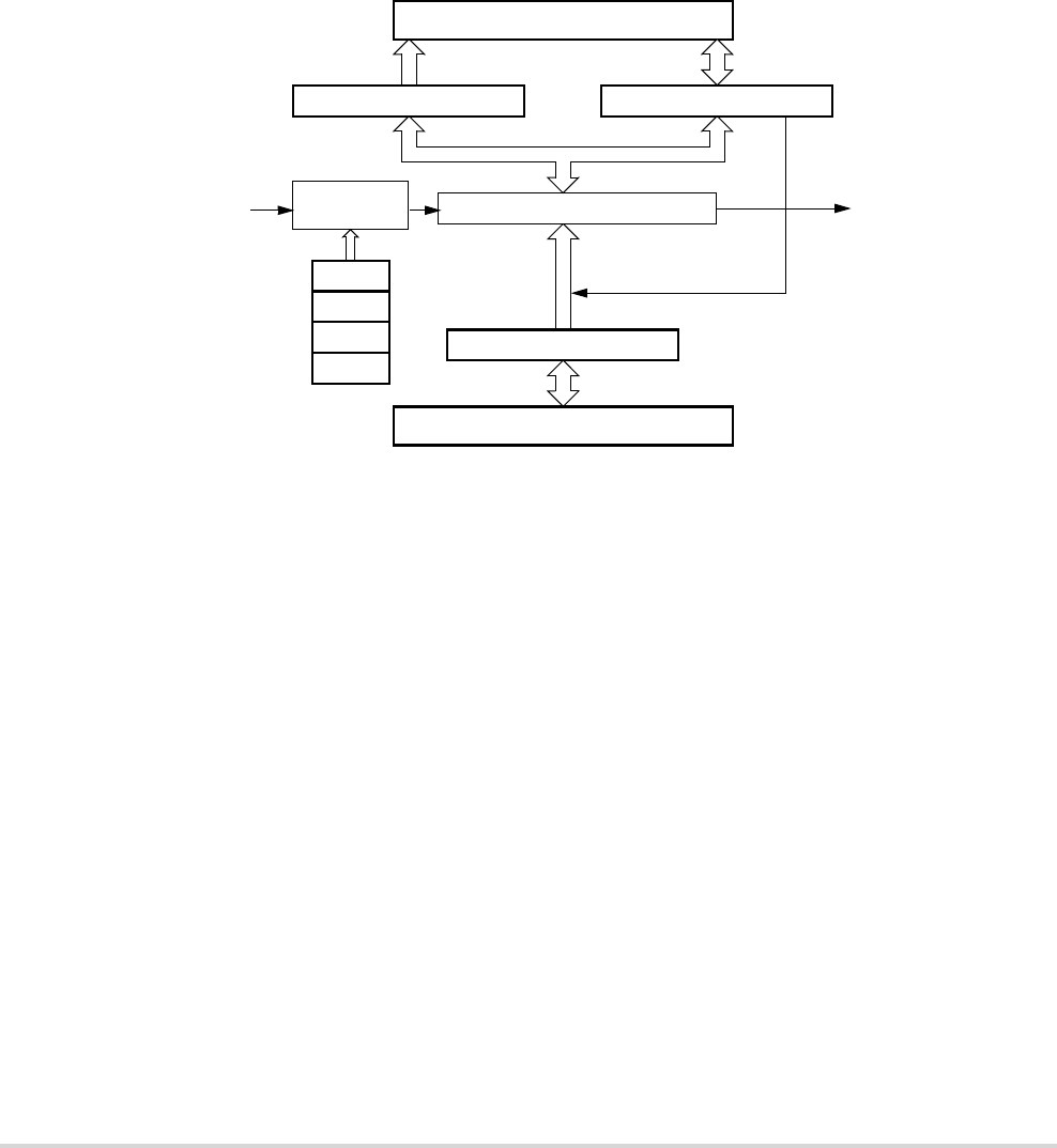
18-2 MCF5282 User’s Manual MOTOROLA
Block Diagram
In halted mode with the WCR[HALTED] bit set, watchdog timer module operation stops.
In halted mode with the WCR[HALTED] bit cleared, the watchdog timer continues to
operate normally. When halted mode is exited, watchdog timer operation continues from
the state it was in before entering halted mode, but any updates made in halted mode
remain.
18.3 Block Diagram
Figure 18-1. Watchdog Timer Block Diagram
18.4 Signals
The watchdog timer module has no off-chip signals.
18.5 Memory Map and Registers
This subsection describes the memory map and registers for the watchdog timer. The
watchdog timer has a IPSBAR offset for base address of 0x0014_0000.
18.5.1 Memory Map
Refer to Table 18-2 for an overview of the watchdog memory map.
16-bit WMR
16-bit Watchdog Counter
Count = 0
System Divide by Reset
Clock
IPBUS
8192
16-bit WCNTR 16-bit WSR
IPBUS
Load Counter
EN
WAI T
DOZE
HALTED

MOTOROLA Chapter 18. Watchdog Timer Module 18-3
Memory Map and Registers
18.5.2 Registers
The watchdog timer programming model consists of these registers:
• Watchdog control register (WCR), which configures watchdog timer operation
• Watchdog modulus register (WMR), which determines the timer modulus
reload value
• Watchdog count register (WCNTR), which provides visibility to the watchdog
counter value
• Watchdog service register (WSR), which requires a service sequence to
prevent reset
18.5.2.1 Watchdog Control Register (WCR)
The 16-bit WCR configures watchdog timer operation.
Table 18-2. Watchdog Timer Module Memory Map
IPSBAR Offset Bits 15–8 Bits 7–0 Access 1
1S = CPU supervisor mode access only. S/U = CPU supervisor or user mode access. User mode accesses
to supervisor only addresses have no effect and result in a cycle termination transfer error.
0x0014_0000 Watchdog Control Register (WCR) S
0x0014_0002 Watchdog Modulus Register (WMR) S
0x0014_0004 Watchdog Count Register (WCNTR) S/U
0x0014_0006 Watchdog Service Register (WSR) S/U
15 14 13 12 11 10 9 8
Field —
Reset 0000_0000
R/W R
765 4 3210
Field — WAIT DOZE HALTED EN
Reset 0000_1111
R/W R R/W
Address IPSBAR + 0x0014_0000, 0x0014_0001
Figure 18-2. Watchdog Control Register (WCR)

18-4 MCF5282 User’s Manual MOTOROLA
Memory Map and Registers
18.5.2.2 Watchdog Modulus Register (WMR)
Table 18-3. WCR Field Descriptions
Bit(s) Name Description
15–4 — Reserved, should be cleared.
3 WAIT Wait mode bit. Controls the function of the watchdog timer in wait mode. Once written, the
WAIT bit is not affected by further writes except in halted mode. Reset sets WAIT.
1 Watchdog timer stopped in wait mode
0 Watchdog timer not affected in wait mode
2 DOZE Doze mode bit. Controls the function of the watchdog timer in doze mode. Once written, the
DOZE bit is not affected by further writes except in halted mode. Reset sets DOZE.
1 Watchdog timer stopped in doze mode
0 Watchdog timer not affected in doze mode
1 HALTED Halted mode bit. Controls the function of the watchdog timer in halted mode. Once written, the
HALTED bit is not affected by further writes except in halted mode.
During halted mode, watchdog timer registers can be written and read normally. When halted
mode is exited, timer operation continues from the state it was in before entering halted mode,
but any updates made in halted mode remain. If a write-once register is written for the first time
in halted mode, the register is still writable when halted mode is exited.
1 Watchdog timer stopped in halted mode
0 Watchdog timer not affected in halted mode
Note: Changing the HALTED bit from 1 to 0 during halted mode starts the watchdog timer.
Changing the HALTED bit from 0 to 1 during halted mode stops the watchdog timer.
0 EN Watchdog enable bit. Enables the watchdog timer. Once written, the EN bit is not affected by
further writes except in halted mode. When the watchdog timer is disabled, the watchdog
counter and prescaler counter are held in a stopped state.
1 Watchdog timer enabled
0 Watchdog timer disabled
15 14 13 12 11 10 9 8
Field WM15 WM14 WM13 WM12 WM11 WM10 WM9 WM8
Reset 1111_1111
R/W R/W
765 4 3210
Field WM7 WM6 WM5 WM4 WM3 WM2 WM1 WM0
Reset 1111_1111
R/W R/W
Address IPSBAR + 0x0014_0002, 0x0014_0003
Figure 18-3. Watchdog Modulus Register (WMR)

MOTOROLA Chapter 18. Watchdog Timer Module 18-5
Memory Map and Registers
18.5.2.3 Watchdog Count Register (WCNTR)
18.5.2.4 Watchdog Service Register (WSR)
When the watchdog timer is enabled, writing 0x5555 and then 0xAAAA to WSR before
the watchdog counter times out prevents a reset. If WSR is not serviced before the timeout,
the watchdog timer sends a signal to the reset controller module that sets the RSR[WDR]
bit and asserts a system reset.
Both writes must occur in the order listed before the timeout, but any number of instructions
can be executed between the two writes. However, writing any value other than 0x5555 or
0xAAAA to WSR resets the servicing sequence, requiring both values to be written to keep
the watchdog timer from causing a reset.
Table 18-4. WMR Field Descriptions
Bit(s) Name Description
15–0 WM Watchdog modulus. Contains the modulus that is reloaded into the watchdog counter by a
service sequence. Once written, the WM[15:0] field is not affected by further writes except in
halted mode. Writing to WMR immediately loads the new modulus value into the watchdog
counter. The new value is also used at the next and all subsequent reloads. Reading WMR
returns the value in the modulus register.
Reset initializes the WM[15:0] field to 0xFFFF.
Note: The prescaler counter is reset anytime a new value is loaded into the watchdog counter
and also during reset.
15 14 13 12 11 10 9 8
Field WC15 WC14 WC13 WC12 WC11 WC10 WC9 WC8
Reset 1111_1111
R/W R
765 4 3210
Field WC7 WC6 WC5 WC4 WC3 WC2 WC1 WC0
Reset 1111_1111
R/W R
Address IPSBAR + x0014_0004, 0x0014_0005
Figure 18-4. Watchdog Count Register (WCNTR)
Table 18-5. WCNTR Field Descriptions
Bit(s) Name Description
15–0 WC Watchdog count field. Reflects the current value in the watchdog counter. Reading the 16-bit
WCNTR with two 8-bit reads is not guaranteed to return a coherent value. Writing to WCNTR
has no effect, and write cycles are terminated normally.

18-6 MCF5282 User’s Manual MOTOROLA
Memory Map and Registers
15 14 13 12 11 10 9 8
Field WS15 WS14 WS13 WS12 WS11 WS10 WS9 WS8
Reset 0000_0000
R/W R/W
765 4 3210
Field WS7 WS6 WS5 WS4 WS3 WS2 WS1 WS0
Reset 0000_0000
R/W R/W
Address IPSBAR + 0x0014_0006, 0x0014_0007
Figure 18-5. Watchdog Service Register (WSR)
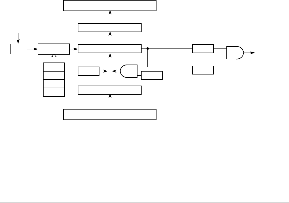
MOTOROLA Chapter 19. Programmable Interrupt Timer Modules (PIT0–PIT3) 19-1
Chapter 19
Programmable Interrupt Timer Modules
(PIT0–PIT3)
19.1 Overview
The programmable interrupt timer (PIT) is a 16-bit timer that provides precise interrupts at
regular intervals with minimal processor intervention. The timer can either count down
from the value written in the modulus register, or it can be a free-running down-counter.
This device has four programmable interrupt timers, PIT0–PIT3.
19.2 Block Diagram
Figure 19-1. PIT Block Diagram
16-bit PMR
16-bit PIT Counter COUNT = 0
System
Clock
IPBUS
16-bit PCNTR
IPBUS
EN OVW
DOZE
HALTED
Prescaler
PRE[3:0] RLD
PIF
PIE
Load
Counter
To Interrupt
Controller
Divide
by 2
19-2 MCF5282 User’s Manual MOTOROLA
Low-Power Mode Operation
19.3 Low-Power Mode Operation
This subsection describes the operation of the PIT modules in low-power modes and halted
mode of operation. Low-power modes are described in the Power Management Module.
Table 19-1 shows the PIT module operation in low-power modes, and how it can exit from
each mode.
NOTE
The low-power interrupt control register (LPICR) in the
System Control Module specifies the interrupt level at or above
which the device can be brought out of a low-power mode.
Table 19-1. PIT Module Operation in Low-power Modes
In wait mode, the PIT module continues to operate as in run mode and can be configured
to exit the low-power mode by generating an interrupt request. In doze mode with the
PCSR[DOZE] bit set, PIT module operation stops. In doze mode with the PCSR[DOZE]
bit cleared, doze mode does not affect PIT operation. When doze mode is exited, the PIT
continues to operate in the state it was in prior to doze mode. In stop mode, the system clock
is absent, and PIT module operation stops.
In halted mode with the PCSR[HALTED] bit set, PIT module operation stops. In halted
mode with the PCSR[HALTED] bit cleared, halted mode does not affect PIT operation.
When halted mode is exited, the PIT continues to operate in its pre-halted mode state, but
any updates made in halted mode remain.
19.4 Signals
The PIT module has no off-chip signals.
Low-power Mode PIT Operation Mode Exit
Wait Normal if PCR[WAIT] cleared,
stopped otherwise
Any IRQx Interrupt at or above level in LPICR
Doze Normal if PCR[DOZE] cleared,
stopped otherwise
Any IRQx Interrupt at or above level in LPICR
Stop Stopped No
Halted Normal if PCR[HALTED] cleared,
stopped otherwise
No. Any IRQx Interrupt will be serviced upon normal
exit from halted mode

MOTOROLA Chapter 19. Programmable Interrupt Timer Modules (PIT0–PIT3) 19-3
Memory Map and Registers
19.5 Memory Map and Registers
This subsection describes the memory map and register structure for PIT0–PIT3.
19.5.1 Memory Map
Refer to Table 19-2 for a description of the memory map.
This device has four programmable interrupt timers with the following IPSBAR offset for
base address locations for each timer.
PIT0: 0x0015_0000
PIT1: 0x0016_0000
PIT2: 0x0017_0000
PIT3: 0x0018_0000
19.5.2 Registers
The PIT programming model consists of these registers:
• The PIT control and status register (PCSR) configures the timer’s operation.
• The PIT modulus register (PMR) determines the timer modulus reload value.
• The PIT count register (PCNTR) provides visibility to the counter value.
Table 19-2. Programmable Interrupt Timer Modules Memory Map
IPSBAR Offset
for PITx
Address
Bits 15–8 Bits 7–0 Access 1
1S = CPU supervisor mode access only. S/U = CPU supervisor or user mode access. User mode accesses to supervisor
only addresses have no effect and result in a cycle termination transfer error.
0x001x_0000 PIT Control and Status Register (PCSR) S
0x001x_0002 PIT Modulus Register (PMR) S
0x001x_0004 PIT Count Register (PCNTR) S/U
0x001x_0006 Unimplemented 2
2Accesses to unimplemented address locations have no effect and result in a cycle termination transfer error.
—
19-4 MCF5282 User’s Manual MOTOROLA
Memory Map and Registers
19.5.2.1 PIT Control and Status Register (PCSR)
15 12 11 10 9 8
Field — PRE3 PRE2 PRE1 PRE0
Reset 0000_0000
R/W R R/W
765 4 3210
Field — DOZE HALTED OVW PIE PIF RLD EN
Reset 0000_0000
R/W R R/W
Address IPSBAR + 0x0015_0000 and 0x0015_0001 (PIT0); 0x0016_0000 and 0x0016_0001 (PIT1); 0x0017_0000
and 0x0017_0001 (PIT2); 0x0018_0000 and 0x0018_0001 (PIT3)
Figure 19-2. PIT Control and Status Register (PCSR)
Table 19-3. PCSR Field Descriptions
Bit(s) Name Description
15–12 — Reserved, should be cleared.
11–8 PRE Prescaler. The read/write prescaler bits select the system clock divisor to generate the PIT
clock. To accurately predict the timing of the next count, change the PRE[3:0] bits only when
the enable bit (EN) is clear. Changing the PRE[3:0] resets the prescaler counter. System reset
and the loading of a new value into the counter also reset the prescaler counter. Setting the EN
bit and writing to PRE[3:0] can be done in this same write cycle. Clearing the EN bit stops the
prescaler counter.
7—Reserved.
PRE System Clock Divisor PRE System Clock Divisor
0000 2 1000 512
0001 4 1001 1,024
0010 8 1010 2,048
0011 16 1011 4,096
0100 32 1100 8,192
0101 64 1101 16,384
0110 128 1110 32,768
0111 256 1111 65,536

MOTOROLA Chapter 19. Programmable Interrupt Timer Modules (PIT0–PIT3) 19-5
Memory Map and Registers
19.5.2.2 PIT Modulus Register (PMR)
The 16-bit read/write PMR contains the timer modulus value that is loaded into the PIT
counter when the count reaches 0x0000 and the PCSR[RLD] bit is set.
When the PCSR[OVW] bit is set, PMR is transparent, and the value written to PMR is
immediately loaded into the PIT counter. The prescaler counter is reset anytime a new value
is loaded into the PIT counter and also during reset. Reading the PMR returns the value
written in the modulus latch. Reset initializes PMR to 0xFFFF.
6 DOZE Doze mode bit. The read/write DOZE bit controls the function of the PIT in doze mode. Reset
clears DOZE.
0 PIT function not affected in doze mode
1 PIT function stopped in doze mode
When doze mode is exited, timer operation continues from the state it was in before entering
doze mode.
5 HALTED Halted mode bit. Controls the function of the PIT in halted mode. Reset clears HALTED.
During halted mode, register read and write accesses function normally. When halted mode is
exited, timer operation continues from the state it was in before entering halted mode, but any
updates made in halted mode remain.
0 PIT function not affected in halted mode
1 PIT function stopped in halted mode
Note: Changing the HALTED bit from 1 to 0 during halted mode starts the PIT timer. Likewise,
changing the HALTED bit from 0 to 1 during halted mode stops the PIT timer.
4 OVW Overwrite. Enables writing to PMR to immediately overwrite the value in the PIT counter.
0 Value in PMR replaces value in PIT counter when count reaches 0x0000.
1 Writing PMR immediately replaces value in PIT counter.
3 PIE PIT interrupt enable. This read/write bit enables the PIF flag to generate interrupt requests.
0 PIF interrupt requests disabled
1 PIF interrupt requests enabled
2 PIF PIT interrupt flag. This read/write bit is set when the PIT counter reaches 0x0000. Clear PIF by
writing a 1 to it or by writing to PMR. Writing 0 has no effect. Reset clears PIF.
0 PIT count has not reached 0x0000.
1 PIT count has reached 0x0000.
1 RLD Reload bit. The read/write reload bit enables loading the value of PMR into the PIT counter
when the count reaches 0x0000.
0 Counter rolls over to 0xFFFF on count of 0x0000
1 Counter reloaded from PMR on count of 0x0000
0 EN PIT enable bit. Enables PIT operation. When the PIT is disabled, the counter and prescaler are
held in a stopped state. This bit is read anytime, write anytime.
0 PIT disabled
1PIT enabled
Table 19-3. PCSR Field Descriptions (continued)
Bit(s) Name Description

19-6 MCF5282 User’s Manual MOTOROLA
Functional Description
19.5.2.3 PIT Count Register (PCNTR)
The 16-bit, read-only PCNTR contains the counter value. Reading the 16-bit counter with
two 8-bit reads is not guaranteed to be coherent. Writing to PCNTR has no effect, and write
cycles are terminated normally.
19.6 Functional Description
This subsection describes the PIT functional operation.
19.6.1 Set-and-Forget Timer Operation
This mode of operation is selected when the RLD bit in the PCSR register is set.
When the PIT counter reaches a count of 0x0000, the PIF flag is set in PCSR. The value in
the modulus register is loaded into the counter, and the counter begins decrementing toward
0x0000. If the PIE bit is set in PCSR, the PIF flag issues an interrupt request to the CPU.
15 14 13 12 11 10 9 8
Field PM15 PM14 PM13 PM12 PM11 PM10 PM9 PM8
Reset 1111_1111
R/W R/W
765 4 3210
Field PM7 PM6 PM5 PM4 PM3 PM2 PM1 PM0
Reset 1111_1111
R/W R/W
Address IPSBAR + 0x0015_0002 and 0x0015_0003 (PIT0); 0x0016_0002 and 0x0016_0003 (PIT1); 0x0017_0002
and 0x0017_0003 (PIT2); 0x0018_0002 and 0x0018_0003 (PIT3)
Figure 19-3. PIT Modulus Register (PMR)
15 14 13 12 11 10 9 8
Field PC15 PC14 PC13 PC12 PC11 PC10 PC9 PC8
Reset 1111_1111
R/W R
765 4 3210
Field PC7 PC6 PC5 PC4 PC3 PC2 PC1 PC0
Reset 1111_1111
R/W R
Address IPSBAR + 0x0015_0004 and 0x0015_0005 (PIT0), 0x0016_0004 and 0x0016_0005 (PIT1), 0x0017_0004
and 0x0017_0005 (PIT2), 0x0018_0004 and 0x0018_0005 (PIT3)
Figure 19-4. PIT Count Register (PCNTR)
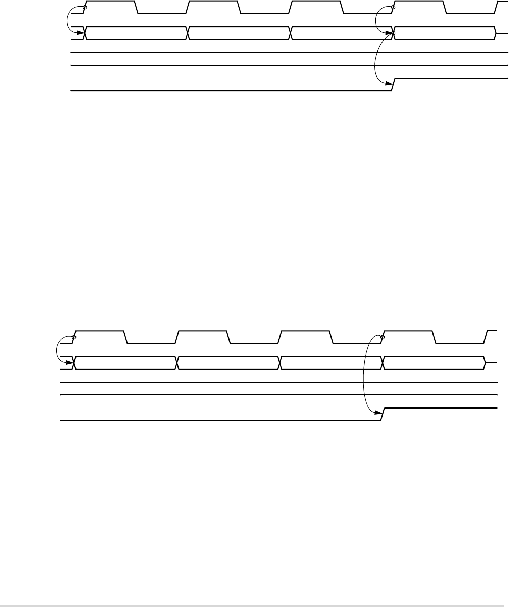
MOTOROLA Chapter 19. Programmable Interrupt Timer Modules (PIT0–PIT3) 19-7
Functional Description
When the OVW bit is set in PCSR, the counter can be directly initialized by writing to PMR
without having to wait for the count to reach 0x0000.
Figure 19-5. Counter Reloading from the Modulus Latch
19.6.2 Free-Running Timer Operation
This mode of operation is selected when the RLD bit in PCSR is clear. In this mode, the
counter rolls over from 0x0000 to 0xFFFF without reloading from the modulus latch and
continues to decrement.
When the counter reaches a count of 0x0000, the PIF flag is set in PCSR. If the PIE bit is
set in PCSR, the PIF flag issues an interrupt request to the CPU.
When the OVW bit is set in PCSR, the counter can be directly initialized by writing to PMR
without having to wait for the count to reach 0x0000.
Figure 19-6. Counter in Free-Running Mode
19.6.3 Timeout Specifications
The 16-bit PIT counter and prescaler supports different timeout periods. The prescaler
divides the system clock as selected by the PRE[3:0] bits in PCSR. The PM[15:0] bits in
PMR select the timeout period.
0x0002 0x0001 0x0000 0x0005
0x0005
PIT CLOCK
COUNTER
MODULUS
PIF
0x0002 0x0001 0x0000 0xFFFF
0x0005
PIT CLOCK
COUNTER
MODULUS
PIF
Timeout period PRE[3:0] (PM[15:0] 1)+2××
system clock
---------------------------------------------------------------------------=

19-8 MCF5282 User’s Manual MOTOROLA
Interrupt Operation
19.7 Interrupt Operation
Table 19-4 shows the interrupt request generated by the PIT.
The PIF flag is set when the PIT counter reaches 0x0000. The PIE bit enables the PIF flag
to generate interrupt requests. Clear PIF by writing a 1 to it or by writing to the PMR.
Table 19-4. PIT Interrupt Requests
Interrupt Request Flag Enable Bit
Timeout PIF PIE

MOTOROLA Chapter 20. General Purpose Timer Modules (GPTA and GPTB) 20-1
Chapter 20
General Purpose Timer Modules
(GPTA and GPTB)
The MCF5282 has two 4-channel general purpose timer modules (GPTA and GPTB). Each
consists of a 16-bit counter driven by a 7-stage programmable prescaler.
A timer overflow function allows software to extend the timing capability of the system
beyond the 16-bit range of the counter. Each of the four timer channels can be configured
for input capture, which can capture the time of a selected transition edge, or for output
compare, which can generate output waveforms and timer software delays. These functions
allow simultaneous input waveform measurements and output waveform generation.
Additionally, one of the channels, channel 3, can be configured as a 16-bit pulse
accumulator that can operate as a simple event counter or as a gated time accumulator. The
pulse accumulator uses the GPT channel 3 input/output pin in either event mode or gated
time accumulation mode.
20.1 Features
Features of the general-purpose timer include:
• Four 16-bit input capture/output compare channels
• 16-bit architecture
• Programmable prescaler
• Pulse widths variable from microseconds to seconds
• Single 16-bit pulse accumulator
• Toggle-on-overflow feature for pulse-width modulator (PWM) generation
• External timer clock input (SYNCA/SYNCB)
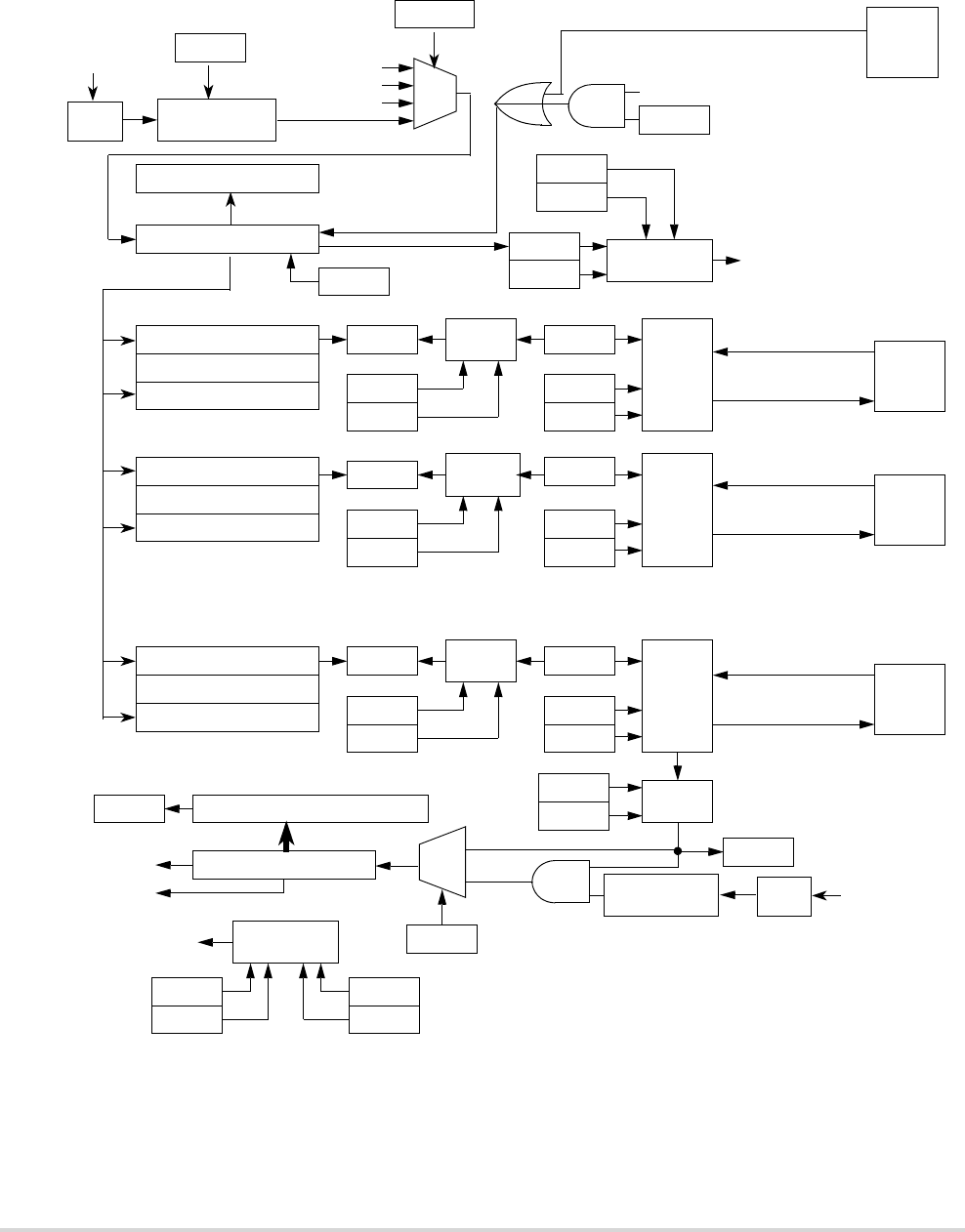
20-2 MCF5282 User’s Manual MOTOROLA
Block Diagram
20.2 Block Diagram
Figure 20-1. GPT Block Diagram
Prescaler
Channel 0
PT0
16-Bit Counter
System
LOGIC
PR[2:0]
Divide-by-64
GPTC0H:GPTC0L
EDGE
DETECT
GPTPACNTH:GPTPACNTL
PAOVF
PEDGE
PAOVI
PAMOD
PAE
16-Bit Comparator
GPTCNTH:GPTCNTL
16-Bit Latch
CHANNEL 1
GPTC1H:GPTC1L
16-Bit Comparator
16-Bit Latch
16-Bit Counter
Interrupt
Logic
TOF
TOI
C0F
C1F
Edge
Detect
PT1
LOGIC
Edge
Detect
CxF
Channel 2
Channel3
GPTC3H:GPTC3L
16-Bit Comparator
16-Bit Latch
C3F
PT3
LOGIC
Edge
Detect
IOS0
IOS1
IOS3
OM:OL0
TOV0
OM:OL1
TOV1
OM:OL3
TOV3
EDG1A
EDG1B
EDG3A
EDG3B
EDG0A
EDG0B
TCRE
Channel 3 Output Compare
PAIF
Clear Counter
PAIF
PAI
Interrupt
Logic
CxI
Interrupt
Request
Interrupt
Request
PAOVF
CH. 3 Compare
CH.3 Capture
CH. 1 Capture
MUX
CLK[1:0]
PACLK
PACLK/256
PACLK/65536
PACLK
PACLK/256
PACLK/65536
TE
Clock
CH. 1 Compare
CH. 0 Compare
CH. 0 Capture
PA Input
MUX
GPTx0
Pin
GPTx1
Pin
GPTx3
Pin
X
SYNCx
Pin
Divide
by 2
Divide
by 2
System
Clock
MOTOROLA Chapter 20. General Purpose Timer Modules (GPTA and GPTB) 20-3
Low-Power Mode Operation
20.3 Low-Power Mode Operation
This subsection describes the operation of the general purpose time module in low-power
modes and halted mode of operation. Low-power modes are described in the Power
Management Module. Table 3-1 shows the general purpose timer module operation in the
low-power modes, and shows how this module may facilitate exit from each mode.
Table 20-1. Watchdog Module Operation in Low-power Modes
General purpose timer operation stops in stop mode. When stop mode is exited, the general
purpose timer continues to operate in its pre-stop mode state.
20.4 Signal Description
Table 20-2 provides an overview of the signal properties.
NOTE
Throughout this section, an “n” in the pin name, as in “GPTn0,”
designates GPTA or GPTB.
20.4.1 GPTn[2:0]
The GPTn[2:0] pins are for channel 2–0 input capture and output compare functions. These
pins are available for general-purpose input/output (I/O) when not configured for timer
functions.
Low-power Mode Watchdog Operation Mode Exit
Wait Normal No
Doze Normal No
Stop Stopped No
Halted Normal No
Table 20-2. Signal Properties
Pin
Name
GPTPORT
Register Bit Function Reset State Pull-up
GPTn0PORTTn0GPTn channel 0 IC/OC pin Input Active
GPTn1PORTTn1GPTn channel 1 IC/OC pin Input Active
GPTn2PORTTn2GPTn channel 2 IC/OC pin Input Active
GPTn3PORTTn3GPTn channel 3 IC/OC or PA pin Input Active
SYNCnPORTE[3:0] 1
1SYNCA is available on either PORTE3 or PORTE1; SYNCB is available on either PORTE2 or
PORTE0.
GPTn counter synchronization Input Active

20-4 MCF5282 User’s Manual MOTOROLA
Memory Map and Registers
20.4.2 GPTn3
The GPTn3 pin is for channel 3 input capture and output compare functions or for the pulse
accumulator input. This pin is available for general-purpose I/O when not configured for
timer functions.
20.4.3 SYNCn
The SYNCn pin is for synchronization of the timer counter. It can be used to synchronize
the counter with externally-timed or clocked events. A high signal on this pin clears the
counter.
20.5 Memory Map and Registers
See Table 20-3 for a memory map of the two GPT modules. GPTA has a base address of
IPSBAR + 0x1A_0000. GPTB has a base address of IPSBAR + 0x1B_0000.
NOTE
Reading reserved or unimplemented locations returns zeroes.
Writing to reserved or unimplemented locations has no effect.
Table 20-3. GPT Modules Memory Map
IPSBAR Offset
Bits 7–0 Access 1
GPTA GPTB
0x1A_0000 0x1B_0000 GPT IC/OC Select Register (GPTIOS) S
0x1A_0001 0x1B_0001 GPT Compare Force Register (GPTCFORC) S
0x1A_0002 0x1B_0002 GPT Output Compare 3 Mask Register (GPTOC3M) S
0x1A_0003 0x1B_0003 GPT Output Compare 3 Data Register (GPTOC3D) S
0x1A_0004 0x1B_0004 GPT Counter Register (GPTCNT) S
0x1A_0006 0x1B_0006 GPT System Control Register 1 (GPTSCR1) S
0x1A_0007 0x1B_0007 Reserved 2 —
0x1A_0008 0x1B_0008 GPT Toggle-on-Overflow Register (GPTTOV) S
0x1A_0009 0x1B_0009 GPT Control Register 1 (GPTCTL1) S
0x1A_000A 0x1B_000a Reserved(2) —
0x1A_000B 0x1B_000b GPT Control Register 2 (GPTCTL2) S
0x1A_000C 0x1B_000c GPT Interrupt Enable Register (GPTIE) S
0x1A_000D 0x1B_000d GPT System Control Register 2 (GPTSCR2) S
0x1A_000E 0x1B_000e GPT Flag Register 1 (GPTFLG1) S
0x1A_000F 0x1B_000f GPT Flag Register 2 (GPTFLG2) S

MOTOROLA Chapter 20. General Purpose Timer Modules (GPTA and GPTB) 20-5
Memory Map and Registers
20.5.1 GPT Input Capture/Output Compare
Select Register (GPTIOS)
0x1A_0010 0x1B_0010 GPT Channel 0 Register High (GPTC0H) S
0x1A_0011 0x1Bb_0011 GPT Channel 0 Register Low (GPTC0L) S
0x1A_0012 0x1B_0012 GPT Channel 1 Register High (GPTC1H) S
0x1A_0013 0x1B_0013 GPT Channel 1 Register Low (GPTC1L) S
0x1A_0014 0x1B_0014 GPT Channel 2 Register High (GPTC2H) S
0x1A_0015 0x1B_0015 GPT Channel 2 Register Low (GPTC2L) S
0x1A_0016 0x1B_0016 GPT Channel 3 Register High (GPTC3H) S
0x1A_0017 0x1B_0017 GPT Channel 3 Register Low (GPTC3L) S
0x1A_0018 0x1B_0018 Pulse Accumulator Control Register (GPTPACTL) S
0x1A_0019 0x1B_0019 Pulse Accumulator Flag Register (GPTPAFLG) S
0x1A_001A 0x1B_001A Pulse Accumulator Counter Register High (GPTPACNTH) S
0x1A_001B 0x1B_001B Pulse Accumulator Counter Register Low (GPTPACNTL) S
0x1A_001C 0x1B_001C Reserved(2) —
0x1A_001D 0x1B_001D GPT Port Data Register (GPTPORT) S
0x1A_001E 0x1B_001E GPT Port Data Direction Register (GPTDDR) S
0x1A_001F 0x1B_001F GPT Test Register (GPTTST) S
1S = CPU supervisor mode access only.
2Writes have no effect, reads return 0s, and the access terminates without a transfer error exception.
7430
Field — IOS
Reset 0000_0000
R/W R/W
Address IPSBAR + 0x401A_0000, 0x401B_0000
Figure 20-2. GPT Input Capture/Output Compare Select Register (GPTIOS)
Table 20-3. GPT Modules Memory Map (continued)
IPSBAR Offset
Bits 7–0 Access 1
GPTA GPTB

20-6 MCF5282 User’s Manual MOTOROLA
Memory Map and Registers
20.5.2 GPT Compare Force Register (GPCFORC)
NOTE
A successful channel 3 output compare overrides any compare
on channels 2:0. For each OC3M bit that is set, the output
compare action reflects the corresponding OC3D bit.
20.5.3 GPT Output Compare 3 Mask Register (GPTOC3M)
Table 20-4. GPTIOS Field Descriptions
Bit(s) Name Description
7–4 — Reserved, should be cleared.
3–0 IOS I/O select. The IOS[3:0] bits enable input capture or output compare operation for the
corresponding timer channels. These bits are read anytime (always read 0x00), write
anytime.
1 Output compare enabled
0 Input capture enabled
7430
Field — FOC
Reset 0000_0000
R/W R/W
Address IPSBAR + 0x1A_00001, 0x1B_0001
Figure 20-3. GPT Input Compare Force Register (GPCFORC)
Table 20-5. GPTCFORC Field Descriptions
Bit(s) Name Description
7–4 — Reserved, should be cleared.
3–0 FOC Force output compare.Setting an FOC bit causes an immediate output compare on the
corresponding channel. Forcing an output compare does not set the output compare
flag. These bits are read anytime, write anytime.
1 Force output compare
0 No effect
7430
Field — OC3M
Reset 0000_0000
R/W R/W
Address IPSBAR + 0x1A_0002, 0x1B_0002
Figure 20-4. GPT Output Compare 3 Mask Register (GPTOC3M)

MOTOROLA Chapter 20. General Purpose Timer Modules (GPTA and GPTB) 20-7
Memory Map and Registers
20.5.4 GPT Output Compare 3 Data Register (GPTOC3D)
NOTE
A successful channel 3 output compare overrides any channel
2:0 compares. For each OC3M bit that is set, the output
compare action reflects the corresponding OC3D bit.
20.5.5 GPT Counter Register (GPTCNT)
Table 20-6. GPTOC3M Field Descriptions
Bit(s) Name Description
7–4 — Reserved, should be cleared.
3–0 OC3M Output compare 3 mask. Setting an OC3M bit configures the corresponding PORTTn
pin to be an output. OC3Mn makes the GPT port pin an output regardless of the data
direction bit when the pin is configured for output compare (IOSx = 1). The OC3Mn bits
do not change the state of the PORTTnDDR bits. These bits are read anytime, write
anytime.
1 Corresponding PORTTn pin configured as output
0 No effect
7430
Field — OC3D
Reset 0000_0000
R/W R/W
Address IPSBAR + 0x1A_0003, 0x1B_0003
Figure 20-5. GPT Output Compare 3 Data Register (GPTOC3D)
Table 20-7. GPTOC3D Field Descriptions
Bit(s) Name Description
7–4 — Reserved, should be cleared.
3–0 OC3D Output compare 3 data. When a successful channel 3 output compare occurs, these
bits transfer to the PORTTn data register if the corresponding OC3Mn bits are set.
These bits are read anytime, write anytime.
15 0
Field CNTR
Reset 0000_0000_0000_0000
R/W Read only
Address IPSBAR + 0x1A_0004, 0x1B_0004
Figure 20-6. GPT Counter Register (GPTCNT)

20-8 MCF5282 User’s Manual MOTOROLA
Memory Map and Registers
20.5.6 GPT System Control Register 1 (GPTSCR1)
Table 20-8. GPTCNT Field Descriptions
Bit(s) Name Description
15–0 CNTR Read-only field that provides the current count of the timer counter. To ensure coherent
reading of the timer counter, such that a timer rollover does not occur between two
back-to-back 8-bit reads, it is recommended that only word (16-bit) accesses be used.
A write to GPTCNT may have an extra cycle on the first count because the write is not
synchronized with the prescaler clock. The write occurs at least one cycle before the
synchronization of the prescaler clock.
These bits are read anytime. They should be written to only in test (special) mode;
writing to them has no effect in normal modes.
7 6543 0
Field GPTEN — TFFCA —
Reset 0000_0000
R/W R/W
Address IPSBAR + 0x1A_0006, 0x1B_0006
Figure 20-7. GPT System Control Register 1 (GPTSCR1)
Table 20-9. GPTSCR1 Field Descriptions
Bit(s) Name Description
7 GPTEN Enables the general purpose timer. When the timer is disabled, only the registers are
accessible. Clearing GPTEN reduces power consumption. These bits are read
anytime, write anytime.
1 GPT enabled
0 GPT and GPT counter disabled
6–5 — Reserved, should be cleared.
4 TFFCA Timer fast flag clear all. Enables fast clearing of the main timer interrupt flag registers
(GPTFLG1 and GPTFLG2) and the PA flag register (GPTPAFLG). TFFCA eliminates
the software overhead of a separate clear sequence. See Figure 20-8.
When TFFCA is set:
• An input capture read or a write to an output compare channel clears the
corresponding channel flag, CxF.
• Any access of the GPT count registers (GPTCNTH/L) clears the TOF flag.
• Any access of the PA counter registers (GPTPACNT) clears both the PAOVF and
PAIF flags in GPTPAFLG.
Writing logic 1s to the flags clears them only when TFFCA is clear.
1 Fast flag clearing
0 Normal flag clearing
3–0 — Reserved, should be cleared.
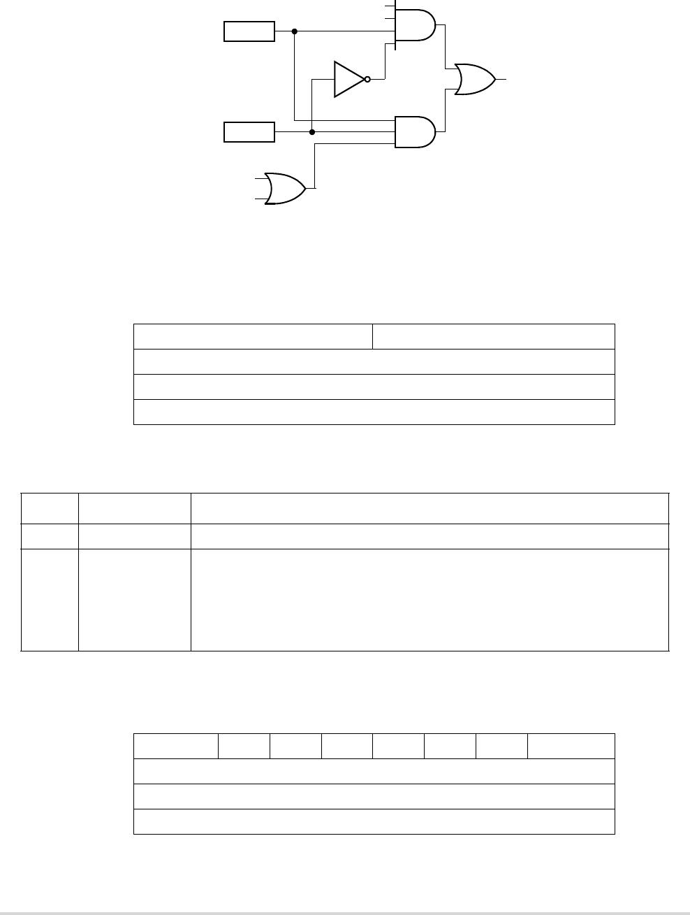
MOTOROLA Chapter 20. General Purpose Timer Modules (GPTA and GPTB) 20-9
Memory Map and Registers
Figure 20-8. Fast Clear Flag Logic
20.5.7 GPT Toggle-On-Overflow Register (GPTTOV)
20.5.8 GPT Control Register 1 (GPTCTL1)
7 6543 0
Field — TOV
Reset 0000_0000
R/W R/W
Address IPSBAR + 0x1A_0008, 0x1B_0008
Figure 20-9. GPT Toggle-On-Overflow Register (GPTTOV)
Table 20-10. GPTTOV Field Description
Bit(s) Name Description
7–4 — Reserved, should be cleared.
3–0 TOV Toggles the output compare pin on overflow for each channel. This feature only takes
effect when in output compare mode. When set, it takes precedence over forced output
compare but not channel 3 override events. These bits are read anytime, write
anytime.
1 Toggle output compare pin on overflow feature enabled
0 Toggle output compare pin on overflow feature disabled
7 654321 0
Field OM3 OL3 OM2 OL2 OM1 OL1 OM0 OL0
Reset 0000_0000
R/W R/W
Address IPSBAR + 0x1A_0009, 0x1B_0009
Figure 20-10. GPT Control Register 1 (GPTCTL1)
Clear
Write GPTCn Registers
Read GPTCn Registers
TFFCA
Data Bit n
Write GPTFLG1 Register
CnF
CnF Flag

20-10 MCF5282 User’s Manual MOTOROLA
Memory Map and Registers
20.5.9 GPT Control Register 2 (GPTCTL2)
20.5.10 GPT Interrupt Enable Register (GPTIE)
Table 20-11. GPTCL1 Field Descriptions
Bit(s) Name Description
7–0 OMx/OLx Output mode/output level. Selects the output action to be taken as a result of a
successful output compare on each channel. When either OMn or OLn is set and the
IOSn bit is set, the pin is an output regardless of the state of the corresponding DDR
bit. These bits are read anytime, write anytime.
00 GPT disconnected from output pin logic
01 Toggle OCn output line
10 Clear OCn output line
11 Set OCn line
Note: Channel 3 shares a pin with the pulse accumulator input pin. To use the PAI
input, clear both the OM3 and OL3 bits and clear the OC3M3 bit in the output compare
3 mask register.
7 654321 0
Field EDG3B EDG3A EDG2B EDG2A EDG1B EDG1A EDG0B EDG0A
Reset 0000_0000
R/W R/W
Address IPSBAR + 0x1A_000B, 0x1B_000B
Figure 20-11. GPT Control Register 2 (GPTCTL2)
Table 20-12. GPTLCTL2 Field Descriptions
Bit(s) Name Description
7–0 EDGn[B:A] Input capture edge control. Configures the input capture edge detector circuits for each
channel. These bits are read anytime, write anytime.
00 Input capture disabled
01 Input capture on rising edges only
10 Input capture on falling edges only
11 Input capture on any edge (rising or falling)
7 6543 0
Field — CI
Reset 0000_0000
R/W R/W
Address IPSBAR + 0x1A_000C, 0x1B_000C
Figure 20-12. GPT Interrupt Enable Register (GPTIE)

MOTOROLA Chapter 20. General Purpose Timer Modules (GPTA and GPTB) 20-11
Memory Map and Registers
20.5.11 GPT System Control Register 2 (GPTSCR2)
Table 20-13. GPTIE Field Descriptions
Bit(s) Name Description
7–4 — Reserved, should be cleared.
3–0 CnI Channel interrupt enable. Enables the C[3:0]F flags in GPT flag register 1 to generate
interrupt requests for each channel. These bits are read anytime, write anytime.
1 Corresponding channel interrupt requests enabled
0 Corresponding channel interrupt requests disabled
7 65432 0
Field TOI — PUPT RDPT TCRE PR
Reset 0000_0000
R/W R/W
Address IPSBAR + 0x1A_000D, 0x1B_000D
Figure 20-13. GPT System Control Register 2 (GPTSCR2)
Table 20-14. GPTSCR2 Field Descriptions
Bit(s) Name Description
7 TOI Enables timer overflow interrupt requests.
1 Overflow interrupt requests enabled
0 Overflow interrupt requests disabled
6 — Reserved, should be cleared.
5 PUPT Enables pull-up resistors on the GPT ports when the ports are configured as inputs.
1 Pull-up resistors enabled
0 Pull-up resistors disabled
4 RDPT GPT drive reduction. Reduces the output driver size.
1 Output drive reduction enabled
0 Output drive reduction disabled
3 TCRE Enables a counter reset after a channel 3 compare.
1 Counter reset enabled
0 Counter reset disabled
Note: When the GPT channel 3 registers contain 0x0000 and TCRE is set, the GPT
counter registers remain at 0x0000 all the time. When the GPT channel 3 registers
contain 0xFFFF and TCRE is set, TOF does not get set even though the GPT counter
registers go from 0xFFFF to 0x0000.
2–0 PRnPrescaler bits. Select the prescaler divisor for the GPT counter.
000 Prescaler divisor 1
001 Prescaler divisor 2
010 Prescaler divisor 4
011 Prescaler divisor 8
100 Prescaler divisor 16
101 Prescaler divisor 32
110 Prescaler divisor 64
111 Prescaler divisor 128
Note: The newly selected prescaled clock does not take effect until the next
synchronized edge of the prescaled clock when the clock count transitions to 0x0000.)

20-12 MCF5282 User’s Manual MOTOROLA
Memory Map and Registers
20.5.12 GPT Flag Register 1 (GPTFLG1)
20.5.13 GPT Flag Register 2 (GPTFLG2)
Note: When the fast flag clear all bit, GPTSCR1[TFFCA], is set, any access to the GPT counter registers clears GPT
flag register 2.
7 6543 0
Field — CF
Reset 0000_0000
R/W R/W
Address IPSBAR + 0x1A_000E, 0x1B_000E
Figure 20-14. GPT Flag Register 1 (GPTFLG1)
Table 20-15. GPTFLG1 Field Descriptions
Bit(s) Name Description
7–4 — Reserved, should be cleared.
3–0 CnF Channel flags. A channel flag is set when an input capture or output compare event
occurs. These bits are read anytime, write anytime (writing 1 clears the flag, writing 0
has no effect).
Note: When the fast flag clear all bit, GPTSCR1[TFFCA], is set, an input capture read
or an output compare write clears the corresponding channel flag. When a channel flag
is set, it does not inhibit subsequent output compares or input captures.
7 6543 0
Field TOF — CF
Reset 0000_0000
R/W R/W
Address IPSBAR + 0x1A_000F, 0x1B_000F
Figure 20-15. GPT Flag Register 2 (GPTFLG2)
Table 20-16. GPTFLG2 Field Descriptions
Bit(s) Name Description
7 TOF Timer overflow flag. Set when the GPT counter rolls over from 0xFFFF to 0x0000. If
the TOI bit in GPTSCR2 is also set, TOF generates an interrupt request. This bit is read
anytime, write anytime (writing 1 clears the flag, and writing 0 has no effect).
1 Timer overflow
0 No timer overflow
Note: When the GPT channel 3 registers contain 0xFFFF and TCRE is set, TOF does
not get set even though the GPT counter registers go from 0xFFFF to 0x0000. When
TOF is set, it does not inhibit subsequent overflow events.
6–4 — Reserved, should be cleared.
3–0 CnF Channel flags. A channel flag is set when an input capture or output compare event
occurs. These bits are read anytime, write anytime (writing 1 clears the flag, writing 0
has no effect).

MOTOROLA Chapter 20. General Purpose Timer Modules (GPTA and GPTB) 20-13
Memory Map and Registers
20.5.14 GPT Channel Registers (GPTCn)
20.5.15 Pulse Accumulator Control Register (GPTPACTL)
15 0
Field CCNT
Reset 0000_0000_0000_0000
R/W R/W
Address IPSBAR + 0x1A_0010, 0x1A_0012, 0x1A_0014, 0x1A_0016,
0x1B_0010, 0x1B_0012, 0x1B_0014, 0x1B_0016
Figure 20-16. GPT Channel[0:3] Register (GPTCn)
Table 20-17. GPTCn Field Descriptions
Bit(s) Name Description
15–0 CCNT When a channel is configured for input capture (IOSn = 0), the GPT channel registers
latch the value of the free-running counter when a defined transition occurs on the
corresponding input capture pin.
When a channel is configured for output compare (IOSn = 1), the GPT channel
registers contain the output compare value.
To ensure coherent reading of the GPT counter, such that a timer rollover does not
occur between back-to-back 8-bit reads, it is recommended that only word (16-bit)
accesses be used. These bits are read anytime, write anytime (for the output compare
channel); writing to the input capture channel has no effect.
7 6543 0
Field — PAE PAMOD PEDGE CLK PAOVI PAI
Reset 0000_0000
R/W R/W
Address IPSBAR + 0x1A_0018, 0x1B_0018
Figure 20-17. Pulse Accumulator Control Register (GPTPACTL)
Table 20-18. GPTPACTL Field Descriptions
Bit(s) Name Description
7 — Reserved, should be cleared.
6 PAE Enables the pulse accumulator.
1 Pulse accumulator enabled
0 Pulse accumulator disabled
Note: The pulse accumulator can operate in event mode even when the GPT enable
bit, GPTEN, is clear.
5 PAMOD Pulse accumulator mode. Selects event counter mode or gated time accumulation
mode.
1 Gated time accumulation mode
0 Event counter mode

20-14 MCF5282 User’s Manual MOTOROLA
Memory Map and Registers
20.5.16 Pulse Accumulator Flag Register (GPTPAFLG)
4 PEDGE Pulse accumulator edge. Selects falling or rising edges on the PAI pin to increment the
counter.
In event counter mode (PAMOD = 0):
1 Rising PAI edge increments counter
0 Falling PAI edge increments counter
In gated time accumulation mode (PAMOD = 1):
1 Low PAI input enables divide-by-64 clock to pulse accumulator and trailing rising
edge on PAI sets PAIF flag.
0 High PAI input enables divide-by-64 clock to pulse accumulator and trailing falling
edge on PAI sets PAIF flag.
Note: The timer prescaler generates the divide-by-64 clock. If the timer is not active,
there is no divide-by-64 clock.
To operate in gated time accumulation mode:
1. Apply logic 0 to RSTI pin.
2. Initialize registers for pulse accumulator mode test.
3. Apply appropriate level to PAI pin.
4. Enable GPT.
3–2 CLK Select the GPT counter input clock. Changing the CLK bits causes an immediate
change in the GPT counter clock input.
00 GPT prescaler clock (When PAE = 0, the GPT prescaler clock is always the GPT
counter clock.)
01 PACLK
10 PACLK/256
11 PACLK/65536
1 PAOVI Pulse accumulator overflow interrupt enable. Enables the PAOVF flag to generate
interrupt requests.
1 PAOVF interrupt requests enabled
0 PAOVF interrupt requests disabled
0 PAI Pulse accumulator input interrupt enable. Enables the PAIF flag to generate interrupt
requests.
1 PAIF interrupt requests enabled
0 PAIF interrupt requests disabled
7210
Field — PAOVF PAIF
Reset 0000_0000
R/W R/W
Address IPSBAR + 0x1A_0019, 0x1B_0019
Figure 20-18. Pulse Accumulator Flag Register (GPTPAFLG)
Table 20-18. GPTPACTL Field Descriptions (continued)
Bit(s) Name Description

MOTOROLA Chapter 20. General Purpose Timer Modules (GPTA and GPTB) 20-15
Memory Map and Registers
NOTE
When the fast flag clear all enable bit, GPTSCR1[TFFCA], is
set, any access to the pulse accumulator counter registers clears
all the flags in GPTPAFLG.
20.5.17 Pulse Accumulator Counter Register (GPTPACNT)
Table 20-19. GPTPAFLG Field Descriptions
Bit(s) Name Description
7–2 — Reserved, should be cleared.
1 PAOVF Pulse accumulator overflow flag. Set when the 16-bit pulse accumulator rolls over from
0xFFFF to 0x0000. If the GPTPACTL[PAOVI] bit is also set, PAOVF generates an
interrupt request. Clear PAOVF by writing a 1 to it. This bit is read anytime, write
anytime. (Writing 1 clears the flag; writing 0 has no effect.)
1 Pulse accumulator overflow
0 No pulse accumulator overflow
0 PAIF Pulse accumulator input flag. Set when the selected edge is detected at the PAI pin.
In event counter mode, the event edge sets PAIF. In gated time accumulation mode,
the trailing edge of the gate signal at the PAI pin sets PAIF. If the PAI bit in GPTPACTL
is also set, PAIF generates an interrupt request. Clear PAIF by writing a 1 to it.
1 Active PAI input
0 No active PAI input
15 0
Field PACNT
Reset 0000_0000_0000_0000
R/W R/W
Address IPSBAR + 0x1A_001A, 0x1B_001B
Figure 20-19. Pulse Accumulator Counter Register (GPTPACNT)
Table 20-20. GPTPACR Field Descriptions
Bit(s) Name Description
15–0 PACNT Contains the number of active input edges on the PAI pin since the last reset.
Note: Reading the pulse accumulator counter registers immediately after an active
edge on the PAI pin may miss the last count since the input first has to be synchronized
with the bus clock.
To ensure coherent reading of the PA counter, such that the counter does not
increment between back-to-back 8-bit reads, it is recommended that only word (16-bit)
accesses be used. These bits are read anytime, write anytime.

20-16 MCF5282 User’s Manual MOTOROLA
Memory Map and Registers
20.5.18 GPT Port Data Register (GPTPORT)
20.5.19 GPT Port Data Direction Register (GPTDDR)
7 6543 0
Field — PORTT
Reset 0000_0000
R/W R/W
Address IPSBAR + 0x1A_001D, 0x1B_001D
Figure 20-20. GPT Port Data Register (GPTPORT)
Table 20-21. GPTPORT Field Descriptions
Bit(s) Name Description
7–4 — Reserved, should be cleared.
3–0 PORTT GPT port input capture/output compare data. Data written to GPTPORT is buffered
and drives the pins only when they are configured as general-purpose outputs.
Reading an input (DDR bit = 0) reads the pin state; reading an output (DDR bit = 1)
reads the latched value. Writing to a pin configured as a GPT output does not change
the pin state. These bits are read anytime (read pin state when corresponding
PORTTn bit is 0, read pin driver state when corresponding GPTDDR bit is 1), write
anytime.
7 6543 0
Field — DDRT
GPT Function — IC/OC
Pulse Accumulator Function — PAI —
Reset 0000_0000
R/W R/W
Address IPSBAR + 0x1A_001E, 0x1B_001E
Figure 20-21. GPT Port Data Direction Register (GPTDDR)
Table 20-22. GPTDDR Field Descriptions
Bit(s) Name Description
7–4 — Reserved, should be cleared.
3–0 DDRT Control the port logic of PORTTn. Reset clears the PORTTn data direction register,
configuring all GPT port pins as inputs. These bits are read anytime, write anytime.
1 Corresponding pin configured as output
0 Corresponding pin configured as input

MOTOROLA Chapter 20. General Purpose Timer Modules (GPTA and GPTB) 20-17
Functional Description
20.6 Functional Description
The General Purpose Timer (GPT) module is a 16-bit, 4-channel timer with input capture
and output compare functions and a pulse accumulator.
20.6.1 Prescaler
The prescaler divides the module clock by 1, 2, 4, 8, 16, 32, 64, or 128. The PR[2:0] bits in
GPTSCR2 select the prescaler divisor.
20.6.2 Input Capture
Clearing an I/O select bit, IOSn, configures channel n as an input capture channel. The
input capture function captures the time at which an external event occurs. When an active
edge occurs on the pin of an input capture channel, the timer transfers the value in the GPT
counter into the GPT channel registers, GPTCn.
The minimum pulse width for the input capture input is greater than two module clocks.
The input capture function does not force data direction. The GPT port data direction
register controls the data direction of an input capture pin. Pin conditions such as rising or
falling edges can trigger an input capture only on a pin configured as an input.
An input capture on channel n sets the CnF flag. The CnI bit enables the CnF flag to
generate interrupt requests.
20.6.3 Output Compare
Setting an I/O select bit, IOSn, configures channel n as an output compare channel. The
output compare function can generate a periodic pulse with a programmable polarity,
duration, and frequency. When the GPT counter reaches the value in the channel registers
of an output compare channel, the timer can set, clear, or toggle the channel pin. An output
compare on channel n sets the CnF flag. The CnI bit enables the CnF flag to generate
interrupt requests.
The output mode and level bits, OMn and OLn, select, set, clear, or toggle on output
compare. Clearing both OMn and OLn disconnects the pin from the output logic.
Setting a force output compare bit, FOCn, causes an output compare on channel n. A forced
output compare does not set the channel flag.
A successful output compare on channel 3 overrides output compares on all other output
compare channels. A channel 3 output compare can cause bits in the output compare 3 data
register to transfer to the GPT port data register, depending on the output compare 3 mask
register. The output compare 3 mask register masks the bits in the output compare 3 data
register. The GPT counter reset enable bit, TCRE, enables channel 3 output compares to

20-18 MCF5282 User’s Manual MOTOROLA
Functional Description
reset the GPT counter. A channel 3 output compare can reset the GPT counter even if the
OC3/PAI pin is being used as the pulse accumulator input.
An output compare overrides the data direction bit of the output compare pin but does not
change the state of the data direction bit.
Writing to the PORTTn bit of an output compare pin does not affect the pin state. The value
written is stored in an internal latch. When the pin becomes available for general-purpose
output, the last value written to the bit appears at the pin.
20.6.4 Pulse Accumulator
The pulse accumulator (PA) is a 16-bit counter that can operate in two modes:
1. Event counter mode: counts edges of selected polarity on the pulse accumulator
input pin, PAI
2. Gated time accumulation mode: counts pulses from a divide-by-64 clock
The PA mode bit, PAMOD, selects the mode of operation.
The minimum pulse width for the PAI input is greater than two module clocks.
20.6.5 Event Counter Mode
Clearing the PAMOD bit configures the PA for event counter operation. An active edge on
the PAI pin increments the PA. The PA edge bit, PEDGE, selects falling edges or rising
edges to increment the PA.
An active edge on the PAI pin sets the PA input flag, PAIF. The PA input interrupt enable
bit, PAI, enables the PAIF flag to generate interrupt requests.
NOTE
The PAI input and GPT channel 3 use the same pin. To use the
PAI input, disconnect it from the output logic by clearing the
channel 3 output mode and output level bits, OM3 and OL3.
Also clear the channel 3 output compare 3 mask bit, OC3M3.
The PA counter register, GPTPACNT, reflects the number of active input edges on the PAI
pin since the last reset.
The PA overflow flag, PAOVF, is set when the PA rolls over from 0xFFFF to 0x0000. The
PA overflow interrupt enable bit, PAOVI, enables the PAOVF flag to generate interrupt
requests.
NOTE
The PA can operate in event counter mode even when the GPT
enable bit, GPTEN, is clear.
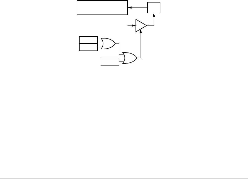
MOTOROLA Chapter 20. General Purpose Timer Modules (GPTA and GPTB) 20-19
Functional Description
20.6.6 Gated Time Accumulation Mode
Setting the PAMOD bit configures the PA for gated time accumulation operation. An active
level on the PAI pin enables a divide-by-64 clock to drive the PA. The PA edge bit, PEDGE,
selects low levels or high levels to enable the divide-by-64 clock.
The trailing edge of the active level at the PAI pin sets the PA input flag, PAIF. The PA input
interrupt enable bit, PAI, enables the PAIF flag to generate interrupt requests.
NOTE
The PAI input and GPT channel 3 use the same pin. To use the
PAI input, disconnect it from the output logic by clearing the
channel 3 output mode and output level bits, OM3 and OL3.
Also clear the channel 3 output compare mask bit, OC3M3.
The PA counter register, GPTPACNT, reflects the number of pulses from the divide-by-64
clock since the last reset.
NOTE
The GPT prescaler generates the divide-by-64 clock. If the
timer is not active, there is no divide-by-64 clock.
Figure 20-22. Channel 3 Output Compare/Pulse Accumulator Logic
20.6.7 General-Purpose I/O Ports
An I/O pin used by the timer defaults to general-purpose I/O unless an internal function
which uses that pin is enabled.
The PORTTn pins can be configured for either an input capture function or an output
compare function. The IOSn bits in the GPT IC/OC select register configure the PORTTn
pins as either input capture or output compare pins.
The PORTTn data direction register controls the data direction of an input capture pin.
External pin conditions trigger input captures on input capture pins configured as inputs.
PAD
OM3
OL3
CHANNEL 3 OUTPUT COMPARE
PULSE
ACCUMULATOR
OC3M3

20-20 MCF5282 User’s Manual MOTOROLA
Functional Description
To configure a pin for input capture:
1. Clear the pin’s IOS bit in GPTIOS.
2. Clear the pin’s DDR bit in PORTTnDDR.
3. Write to GPTCTL2 to select the input edge to detect.
PORTTnDDR does not affect the data direction of an output compare pin. The output
compare function overrides the data direction register but does not affect the state of the
data direction register.
To configure a pin for output compare:
1. Set the pin’s IOS bit in GPTIOS.
2. Write the output compare value to GPTCn.
3. Clear the pin’s DDR bit in PORTTnDDR.
4. Write to the OMn/OLn bits in GPTCTL1 to select the output action.
Table 20-23 shows how various timer settings affect pin functionality.
Table 20-23. GPT Settings and Pin Functions
GPTEN DDR 1 GPTIOS EDGx
[B:A]
OMx/
OLx 2 OC3Mx 3
Pin
Data
Dir.
Pin
Driven
by
Pin
Function Comments
00X
4 X X X In Ext. Digital input GPT disabled by GPTEN = 0
0 1 X X X X Out Data reg. Digital output GPT disabled by GPTEN = 0
1 0 0 (IC) 0 (IC
disable
d)
X 0 In Ext. Digital input Input capture disabled by EDGn
setting
1 1 0 0 X 0 Out Data reg. Digital output Input capture disabled by EDGn
setting
1 0 0 <> 0 X 0 In Ext. IC and
digital input
Normal settings for input capture
1 1 0 <> 0 X 0 Out Data reg. Digital output Input capture of data driven to output
pin by CPU
1 0 0 <> 0 X 1 In Ext. IC and
digital input
OC3M setting has no effect because
IOS = 0
1 1 0 <> 0 X 1 Out Data reg. Digital output OC3M setting has no effect because
IOS = 0; input capture of data driven
to output pin by CPU
101 (OC)X
(3) 0 5 0 In Ext. Digital input Output compare takes place but
does not affect the pin because of
the OMn/OLn setting
1 1 1 X 0 0 Out Data reg. Digital output Output compare takes place but
does not affect the pin because of
the OMn/OLn setting
1 0 1 X <> 0 0 Out OC action Output compare Pin readable only if DDR = 0(5)

MOTOROLA Chapter 20. General Purpose Timer Modules (GPTA and GPTB) 20-21
Reset
20.7 Reset
Reset initializes the GPT registers to a known startup state as described in Section 20.5,
“Memory Map and Registers.”
20.8 Interrupts
Table 20-24 lists the interrupt requests generated by the timer.
1 1 1 X <> 0 0 Out OC action Output compare Pin driven by OC action(5)
1 0 1 X X 1 Out OC action/
OC3Dn
Output compare
(ch 3)
Pin readable only if DDR = 0 6
1 1 1 X X 1 Out OC action/
OC3Dn
Output compare/
OC3Dn
(ch 3)
Pin driven by channel OC action and
OC3Dn via channel 3 OC(6)
1When DDR set the pin as input (0), reading the data register will return the state of the pin. When DDR set the pin as output (1),
reading the data register will return the content of the data latch. Pin conditions such as rising or falling edges can trigger an input
capture on a pin configured as an input.
2OMn/OLn bit pairs select the output action to be taken as a result of a successful output compare. When either OMn or OLn is
set and the IOSn bit is set, the pin is an output regardless of the state of the corresponding DDR bit.
3Setting an OC3M bit configures the corresponding PORTTn pin to be output. OC3Mn makes the PORTTn pin an output regardless
of the data direction bit when the pin is configured for output compare (IOSn = 1). The OC3Mn bits do not change the state of the
PORTTnDDR bits.
4X = Don’t care
5An output compare overrides the data direction bit of the output compare pin but does not change the state of the data direction
bit. Enabling output compare disables data register drive of the pin.
6A successful output compare on channel 3 causes an output value determined by OC3Dn value to temporarily override the output
compare pin state of any other output compare channel.The next OC action for the specific channel will still be output to the pin.
A channel 3 output compare can cause bits in the output compare 3 data register to transfer to the GPT port data register,
depending on the output compare 3 mask register.
Table 20-24. GPT Interrupt Requests
Interrupt Request Flag Enable Bit
Channel 3 IC/OC C3F C3I
Channel 2 IC/OC C2F C2I
Channel 1 IC/OC C1F C1I
Channel 0 IC/OC C0F C0I
PA overflow PAOVF PAOVI
PA input PAIF PAI
Timer overflow TOF TOI
Table 20-23. GPT Settings and Pin Functions (continued)

20-22 MCF5282 User’s Manual MOTOROLA
Interrupts
20.8.1 GPT Channel Interrupts (CnF)
A channel flag is set when an input capture or output compare event occurs. Clear a channel
flag by writing a 1 to it.
NOTE
When the fast flag clear all bit, GPTSCR1[TFFCA], is set, an
input capture read or an output compare write clears the
corresponding channel flag.
When a channel flag is set, it does not inhibit subsequent output
compares or input captures
20.8.2 Pulse Accumulator Overflow (PAOVF)
PAOVF is set when the 16-bit pulse accumulator rolls over from 0xFFFF to 0x0000. If the
PAOVI bit in GPTPACTL is also set, PAOVF generates an interrupt request. Clear PAOVF
by writing a 1 to this flag.
NOTE
When the fast flag clear all enable bit, GPTSCR1[TFFCA], is
set, any access to the pulse accumulator counter registers clears
all the flags in GPTPAFLG.
20.8.3 Pulse Accumulator Input (PAIF)
PAIF is set when the selected edge is detected at the PAI pin. In event counter mode, the
event edge sets PAIF. In gated time accumulation mode, the trailing edge of the gate signal
at the PAI pin sets PAIF. If the PAI bit in GPTPACTL is also set, PAIF generates an interrupt
request. Clear PAIF by writing a 1 to this flag.
NOTE
When the fast flag clear all enable bit, GPTSCR1[TFFCA], is
set, any access to the pulse accumulator counter registers clears
all the flags in GPTPAFLG.
20.8.4 Timer Overflow (TOF)
TOF is set when the GPT counter rolls over from 0xFFFF to 0x0000. If the GPTSCR2[TOI]
bit is also set, TOF generates an interrupt request. Clear TOF by writing a 1 to this flag.

MOTOROLA Chapter 20. General Purpose Timer Modules (GPTA and GPTB) 20-23
Interrupts
NOTE
When the GPT channel 3 registers contain 0xFFFF and TCRE
is set, TOF does not get set even though the GPT counter
registers go from 0xFFFF to 0x0000.
When the fast flag clear all bit, GPTSCR1[TFFCA], is set, any
access to the GPT counter registers clears GPT flag register 2.
When TOF is set, it does not inhibit future overflow events.

20-24 MCF5282 User’s Manual MOTOROLA
Interrupts

MOTOROLA Chapter 21. DMA Timers (DTIM0–DTIM3) 21-1
Chapter 21
DMA Timers (DTIM0–DTIM3)
This chapter describes the configuration and operation of the four Direct Memory Access
(DMA) timer modules (DTIM0, DTIM1, DTIM2, and DTIM3). These 32-bit timers
provide input capture and reference compare capabilities with optional signaling of events
using interrupts or triggers. Additionally, programming examples are included.
NOTE
The designation “n” is used throughout this section to refer to
registers or signals associated with one of the four identical
timer modules—DTIM0, DTIM1, DTIM2, or DTIM3.
21.1 Overview
Each DMA timer module has a separate register set for configuration and control. The
timers can be configured to operate from the system clock or from an external clocking
source using the DTINn signal. If the system clock is selected, it can be divided by 16 or 1.
The selected clock source is routed to an 8-bit programmable prescaler that clocks the
actual DMA timer counter register (DTCNn). Using the DTMRn, DTXMRn, DTCRn, and
DTRRn registers, the DMA timer may be configured to assert an output signal, generate an
interrupt, or initiate a DMA transfer on a particular event.
Figure 21-1 is a block diagram of one of the four identical timer modules.
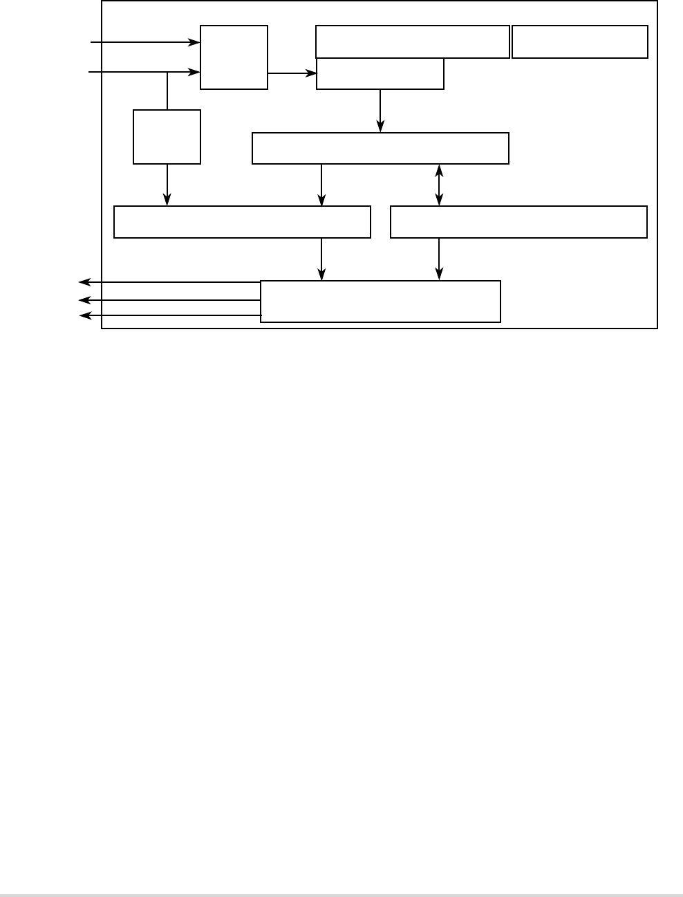
21-2 MCF5282 User’s Manual MOTOROLA
DMA Timer Programming Model
Figure 21-1. DMA Timer Block Diagram
21.1.1 Key Features
Each DMA timer module has the following features:
• Maximum timeout period of 266,521 seconds at 66 MHz (~74 hours)
• 15-ns resolution at 66 MHz
• Programmable sources for the clock input, including external clock
• Programmable prescaler
• Input-capture capability with programmable trigger edge on input pin
• Programmable mode for the output pin on reference compare
• Free run and restart modes
• Programmable interrupt or DMA request on input capture or reference-compare
21.2 DMA Timer Programming Model
The following features are programmable through the timer registers, shown in Table 21-1:
21.2.1 Prescaler
The prescaler clock input is selected from system clock (divided by 1 or 16) or from the
corresponding timer input, DTINn. DTINn is synchronized to the system clock. The
synchronization delay is between two and three system clocks. The corresponding
DMA Timer
Divider
DMA Timer Mode Register (DTMRn)
Prescaler Mode Bits
DMA Timer Counter Register (DTCNn)
31 0
DMA Timer Reference Register (DTRRn)
31 0
DMA Timer Capture Register (DTCRn)
31 0
DMA Timer Event Register (DTERn)
Capture
Detection
DTINn
DTOUTn
clock
(contains incrementing value)
(reference value for comparison with DTCN)(latches DTCN value when triggered by DTINn)
(indicates capture or when DTCN = DTRRn)
IRQn
Clock
Generator
System Clock
(÷1 or ÷16)DMA Timer Extended Mode
Register (DTXMRn)
DREQn
0
0
15 7
70

MOTOROLA Chapter 21. DMA Timers (DTIM0–DTIM3) 21-3
DMA Timer Programming Model
DTMRn[CLK] selects the clock input source. A programmable prescaler divides the clock
input by values from 1 to 256. The prescaler output is an input to the 32-bit counter,
DTCNn.
21.2.2 Capture Mode
Each DMA timer has a 32-bit timer capture register (DTCRn) that latches the counter value
when the corresponding input capture edge detector senses a defined DTINn transition. The
capture edge bits (DTMRn[CE]) select the type of transition that triggers the capture and
sets the timer event register capture event bit, DTERn[CAP]. If DTERn[CAP] is set and
DTXMRn[DMAEN] is one, a DMA request is asserted. If DTERn[CAP] is set and
DTXMRn[DMAEN] is zero, an interrupt is asserted.
21.2.3 Reference Compare
Each DMA timer can be configured to count up to a reference value, at which point
DTERn[REF] is set. If DTMRn[ORRI] is one and DTXMRn[DMAEN] is zero, an interrupt
is asserted. If DTMRn[ORRI] is one and DTXMRn[DMAEN] is one, a DMA request is
asserted. If the free run/restart bit DTMRn[FRR] is set, a new count starts. If it is clear, the
timer keeps running.
21.2.4 Output Mode
When a timer reaches the reference value selected by DTRR, it can send an output signal
on DTOUTn. DTOUTn can be an active-low pulse or a toggle of the current output as
selected by the TMRn[OM] bit.
21.2.5 Memory Map
The timer module registers, shown in Table 21-1, can be modified at any time.
Table 21-1. DMA Timer Module Memory Map
IPSBAR
Offset [31:24] [23:16] [15:8] [7:0]
0x400 DMA Timer0 Mode Register (DTMR0) DMA Timer0 Extended
Mode Register (DTXMR0)
DMA Timer0 Event
Register (DTER0)
0x404 DMA Timer0 Reference Register (DTRR0)
0x408 DMA Timer0 Capture Register (DTCR0)
0x40C DMA Timer0 Counter Register (DTCN0)
0x440 DMA Timer1 Mode Register (DTMR1) DMA Timer1 Extended
Mode Register (DTXMR1)
DMA Timer1 Event
Register (DTER1)
0x444 DMA Timer1 Reference Register (DTRR1)
21-4 MCF5282 User’s Manual MOTOROLA
DMA Timer Programming Model
21.2.6 DMA Timer Mode Registers (DTMRn)
DTMRs, shown in Figure 21-2, program the prescaler and various timer modes.
0x448 DMA Timer1 Capture Register (DTCR1)
0x44C DMA Timer1 Counter Register (DTCN1)
0x480 DMA Timer2 Mode Register (TMR2) DMA Timer2 Extended
Mode Register (DTXMR2)
DMA Timer2 Event
Register (DTER2)
0x484 DMA Timer2 Reference Register (DTRR2)
0x488 DMA Timer2 Capture Register (DTCR2)
0x48C DMA Timer2 Counter Register (DTCN2)
0x4C0 DMA Timer3 Mode Register (TMR3) DMA Timer3 Extended
Mode Register (DTXMR3)
DMA Timer3 Event
Register (DTER3)
0x4C4 DMA Timer3 Reference Register (DTRR3)
0x4C8 DMA Timer3 Capture Register (DTCR3)
0x4CC DMA Timer3 Counter Register (DTCN3)
15 8765 4 3210
Field PS CE OM ORRI FRR CLK RST
Reset 0000_0000_0000_0000
R/W R/W
Address IPSBAR + 0x400 (DTMR0); + 0x440 (DTMR1); + 0x480 (DTMR2); + 0x4C0 (DTMR3)
Figure 21-2. DTMRn Bit Definitions
Table 21-1. DMA Timer Module Memory Map (continued)
IPSBAR
Offset [31:24] [23:16] [15:8] [7:0]

MOTOROLA Chapter 21. DMA Timers (DTIM0–DTIM3) 21-5
DMA Timer Programming Model
Table 21-2 describes the DTMRn fields.
21.2.7 DMA Timer Extended Mode Registers (DTXMRn)
DTXMRs, shown in Figure 21-3, program DMA request and increment modes for the
timers.
Table 21-2. DTMRn Field Descriptions
Bits Name Description
15–8 PS Prescaler value. The prescaler is programmed to divide the clock input (system clock/(16 or 1) or clock on
DTINn) by values from 1 (PS = 0x00) to 256 (PS = 0xFF).
7–6 CE Capture edge.
00 Disable capture event output
01 Capture on rising edge only
10 Capture on falling edge only
11 Capture on any edge
5 OM Output mode.
0 Active-low pulse for one system clock cycle (15 ns at 66 MHz).
1 Toggle output.
4 ORRI Output reference request, interrupt enable. If ORRI is set when DTERn[REF] = 1, a DMA request or an interrupt
occurs, depending on the value of DTXMRn[DMAEN] (DMA request if =1, interrupt if =0).
0 Disable DMA request or interrupt for reference reached (does not affect DMA request or interrupt on capture
function).
1 Enable DMA request or interrupt upon reaching the reference value.
3 FRR Free run/restart
0 Free run. Timer count continues to increment after reaching the reference value.
1 Restart. Timer count is reset immediately after reaching the reference value.
2–1 CLK Input clock source for the timer
00 Stop count
01 System clock divided by 1
10 System clock divided by 16. Note that this clock source is not synchronized with the timer; thus successive
time-outs may vary slightly.
11 DTINn pin (falling edge)
0 RST Reset timer. Performs a software timer reset similar to an external reset, although other register values can still
be written while RST = 0. A transition of RST from 1 to 0 resets register values. The timer counter is not clocked
unless the timer is enabled.
0 Reset timer (software reset)
1 Enable timer
76 1 0
Field DMAEN — MODE16
Reset 0000_0000
R/W R/W
Address IPSBAR + 0x402 (DTXMR0); + 0x442 (DTXMR1); + 0x482 (DTXMR2); + 0x4C2
(DTXMR3)
Figure 21-3. DTXMRn Bit Definitions
21-6 MCF5282 User’s Manual MOTOROLA
DMA Timer Programming Model
Table 21-3 describes the DTXMRn fields.
21.2.8 DMA Timer Event Registers (DTERn)
DTERs, shown in Figure 21-4, reports capture or reference events by setting DTERn[CAP]
or DTERn[REF]. This reporting is done regardless of the corresponding DMA request or
interrupt enable values, DTXMRn[DMAEN] and DTMRn[ORRI,CE].
Writing a 1 to either DTERn[REF] or DTERn[CAP] clears it (writing a 0 does not affect
bit value); both bits can be cleared at the same time. If configured to generate an interrupt
request, the REF and CAP bits must be cleared early in the interrupt service routine so the
timer module can negate the IRQn request signal to the interrupt controller. If configured
to generate a DMA request, the processing of the DMA data transfer automatically clears
both the REF and CAP flags via the internal DMA ACK signal.
Table 21-3. DTXMRn Field Descriptions
Bits Name Description
7 DMAEN DMA request. Enables DMA request output on counter reference match or capture edge event.
0 DMA request disabled
1 DMA request enabled
6–1 — Reserved, should be cleared.
0 MODE16 Selects the increment mode for the timer. MODE16 = 1 is intended to exercise the upper bits of the 32-bit timer
in diagnostic software without requiring the timer to count through its entire dynamic range. This bit puts
the timer in a 16-bit mode in which only the upper 16 bits of the DTCN, DTRR, and DTCR are applicable
to the timer function.
0 Increment timer by 1
1 Increment timer by 65,537
7210
Field — REF CAP
Reset 0000_0000
R/W R/W (ones clear/zeros have no effect)
Address IPSBAR + 0x403 (DTER0); + 0x443 (DTER1); 0x483 (DTER2); + 0x4C3 (DTER3)
Figure 21-4. DTERn Bit Definitions

MOTOROLA Chapter 21. DMA Timers (DTIM0–DTIM3) 21-7
DMA Timer Programming Model
Table 21-4 describes the DTERn fields.
21.2.9 DMA Timer Reference Registers (DTRRn)
Each DTRRn, shown in Figure 21-5, contains the reference value compared with the
respective free-running timer counter (DTCNn) as part of the output-compare function. The
reference value is not matched until DTCNn equals DTRRn.
=
21.2.10 DMA Timer Capture Registers (DTCRn)
Each DTCRn, shown in Figure 21-6, latches the corresponding DTCNn value during a
capture operation when an edge occurs on DTINn, as programmed in DTMRn. The system
clock is assumed to be the clock source. DTINn cannot simultaneously function as a
clocking source and as an input capture pin. Indeterminate operation will result if DTINn
is set as the clock source when the input capture mode is used.
Table 21-4. DTERn Field Descriptions
Bits Name Description
7–2 — Reserved, should be cleared.
1 REF Output reference event. The counter value, DTCNn equals the reference value, DTRRn. Writing a one to REF
clears the event condition. Writing a zero has no effect.
If REF = 1 and DTMRn[ORRI], DTXMRn[DMAEN]
00 No DMA request or interrupt asserted
01 No DMA request or interrupt asserted
10 Assert an interrupt
11 Assert a DMA request
0 CAP Capture event. The counter value has been latched into DTCRn. Writing a one to CAP clears the event condition.
Writing a zero has no effect.
If CAP = 1 and DTMRn[CE], DTXMRn[DMAEN]
000 Disable capture event output
001 Disable capture event output
010 Capture on rising edge only and issue an interrupt
011 Capture on rising edge only and issue a DMA request
100 Capture on falling edge only and issue an interrupt
101 Capture on falling edge only and issue a DMA request
110 Capture on any edge and issue an interrupt
111 Capture on any edge and issue a DMA request
31 0
Field REF
Reset 1111_1111_1111_1111_1111_1111_1111_1111
R/W R/W
Address IPSBAR + 0x404 (DTRR0);+ 0x444 (DTRR1); + 0x484 (DTRR2); + 0x4C4 (DTRR3)
Figure 21-5. DTRRn Bit Definitions

21-8 MCF5282 User’s Manual MOTOROLA
Using the DMA Timer Modules
21.2.11 DMA Timer Counters (DTCNn)
The current value of the 32-bit DTCNs can be read at anytime without affecting counting.
Writing to DTCNn, shown in Figure 21-7, clears it. The timer counter increments on the
clock source rising edge (system clock ÷ 1, system clock ÷ 16, or DTINn).
21.3 Using the DMA Timer Modules
The general-purpose timer modules are typically used in the following manner, though this
is not necessarily the program order in which these actions must occur:
•The DTMRn and DTXMRn registers are configured for the desired function and
behavior.
— Count and compare to a reference value stored in the DTRRn register
— Capture the timer value on an edge detected on DTINn
— Configure DTOUTn output mode
— Increment counter by 1 or by 65,537 (16-bit mode)
— Enable/disable interrupt or DMA request on counter reference match or capture
edge
•The DTMRn[CLK] register is configured to select the clock source to be routed to
the prescaler.
— System clock (can be divided by 1 or 16)
— DTINn, the maximum value of DTINn is 1/5 of the system clock, as described
in the MCF5282MCF523x Electrical Characteristics.
31 0
Field CAP (32-bit capture counter value)
Reset 0000_0000_0000_0000_0000_0000_0000_0000
R/W R
Address IPSBAR + 0x408 (DTCR0); + 0x448 (DTCR1); + 0x488 (DTCR2); + 0x4C8 (DTCR3)
Figure 21-6. DTCRn Bit Definitions
31 0
Field 32-bit timer counter value count
Reset 0000_0000_0000_0000_0000_0000_0000_0000
R/W R/W (to reset)
Address IPSBAR + 0x40C (DTCN0); + 0x44C (DTCN1); + 0x48C (DTCN2); + 0x4CC (DTCN3)
Figure 21-7. DTCNn Bit Definitions

MOTOROLA Chapter 21. DMA Timers (DTIM0–DTIM3) 21-9
Using the DMA Timer Modules
NOTE
DTINn may not be configured as a clock source when the timer
capture mode is selected or indeterminate operation will result.
• The 8-bit DTMRn[PS] prescaler value is set
•Using DTMRn[RST] the counter is cleared and started
• Timer events are either handled with an interrupt service routine, a DMA request or
by a software polling mechanism
21.3.1 Code Example
The following code provides an example of how to initialize DMA Timer0 and how to use
the timer for counting time-out periods.
DTMR0 EQU IPSBARx+0x400;Timer0 mode register
DTMR1 EQU IPSBARx+0x440 ;Timer1 mode register
DTRR0 EQU IPSBARx+0x404 ;Timer0 reference register
DTRR1 EQU IPSBARx+0x444 ;Timer1 reference register
DTCR0 EQU IPSBARx+0x408 ;Timer0 capture register
DTCR1 EQU IPSBARx+0x448 ;Timer1 capture register
DTCN0 EQU IPSBARx+0x40C ;Timer0 counter register
DTCN1 EQU IPSBARx+0x44C ;Timer1 counter register
DTER0 EQU IPSBARx+0x403 ;Timer0 event register
DTER1 EQU IPSBARx+0x443 ;Timer1 event register
* TMR0 is defined as: *
*[PS] = 0xFF, divide clock by 256
*[CE] = 00 disable capture event output
*[OM] = 0 output=active-low pulse
*[ORRI] = 0, disable ref. match output
*[FRR] = 1, restart mode enabled
*[CLK] = 10, system clock/16
*[RST] = 0, timer0 disabled
move.w #0xFF0C,D0
move.w D0,TMR0
move.l #0x0000,D0;writing to the timer counter with any
move.l DO,TCN0 ;value resets it to zero
move.l #AFAF,DO ;set the timer0 reference to be
move.l #D0,TRR0 ;defined as 0xAFAF
The simple example below uses Timer0 to count time-out loops. A time-out occurs when
the reference value, 0xAFAF, is reached.
timer0_ex
clr.l DO
clr.l D1
clr.l D2

21-10 MCF5282 User’s Manual MOTOROLA
Using the DMA Timer Modules
move.l #0x0000,D0
move.l D0,TCN0 ;reset the counter to 0x0000
move.b #0x03,D0 ;writing ones to TER0[REF,CAP]
move.b D0,TER0 ;clears the event flags
move.w TMR0,D0 ;save the contents of TMR0 while setting
bset #0,D0 ;the 0 bit. This enables timer 0 and starts counting
move.w D0,TMR0 ;load the value back into the register, setting TMR0[RST]
T0_LOOP
move.b TER0,D1 ;load TER0 and see if
btst #1,D1 ;TER0[REF] has been set
beq T0_LOOP
addi.l #1,D2 ;Increment D2
cmp.l #5,D2 ;Did D2 reach 5? (i.e. timer ref has timed)
beq T0_FINISH ;If so, end timer0 example. Otherwise jump back.
move.b #0x02,D0 ;writing one to TER0[REF] clears the event flag
move.b D0,TER0
jmp T0_LOOP
T0_FINISH
HALT ;End processing. Example is finished
21.3.2 Calculating Time-Out Values
The formula below determines time-out periods for various reference values:
Time-out period = (1/clock frequency) x (1 or 16) x (DTMRn[PS] + 1) x (DTRRn[REF])
When calculating time-out periods, add 1 to the prescaler to simplify calculating, because
DTMRn[PS] = 0x00 yields a prescaler of 1 and DTMRn[PS] = 0xFF yields a prescaler of
256. For example, if a 66-MHz timer clock is divided by 16, DTMRn[PS] = 0x7F, and the
timer is referenced at 0xFBC5 (64,453 decimal), the time-out period is as follows:
Time-out period = [1/(66 x 106) x (16) x (127 + 1) x (64,453) = 2.00 s

MOTOROLA Chapter 22. Queued Serial Peripheral Interface (QSPI) Module 22-1
Chapter 22
Queued Serial Peripheral Interface
(QSPI) Module
This chapter describes the queued serial peripheral interface (QSPI) module. Following a
feature set overview is a description of operation including details of the QSPI’s internal
RAM organization. The chapter concludes with the programming model and a timing
diagram.
22.1 Overview
The queued serial peripheral interface module provides a serial peripheral interface with
queued transfer capability. It allows users to queue up to 16 transfers at once, eliminating
CPU intervention between transfers. Transfer RAM in the QSPI is indirectly accessible
using address and data registers.
22.2 Features
• Programmable queue to support up to 16 transfers without user intervention
• Supports transfer sizes of 8 to 16 bits in 1-bit increments
• Four peripheral chip-select lines for control of up to 15 devices
• Baud rates from 129.4 Kbps to 16.67 Mbps at 66 MHz
• Programmable delays before and after transfers
• Programmable QSPI clock phase and polarity
• Supports wraparound mode for continuous transfers
22.3 Module Description
The QSPI module communicates with the integrated ColdFire CPU using internal memory
mapped registers starting at IPSBAR + 0x340. See Section 22.5, “Programming Model.” A
block diagram of the QSPI module is shown in Figure 22-1.
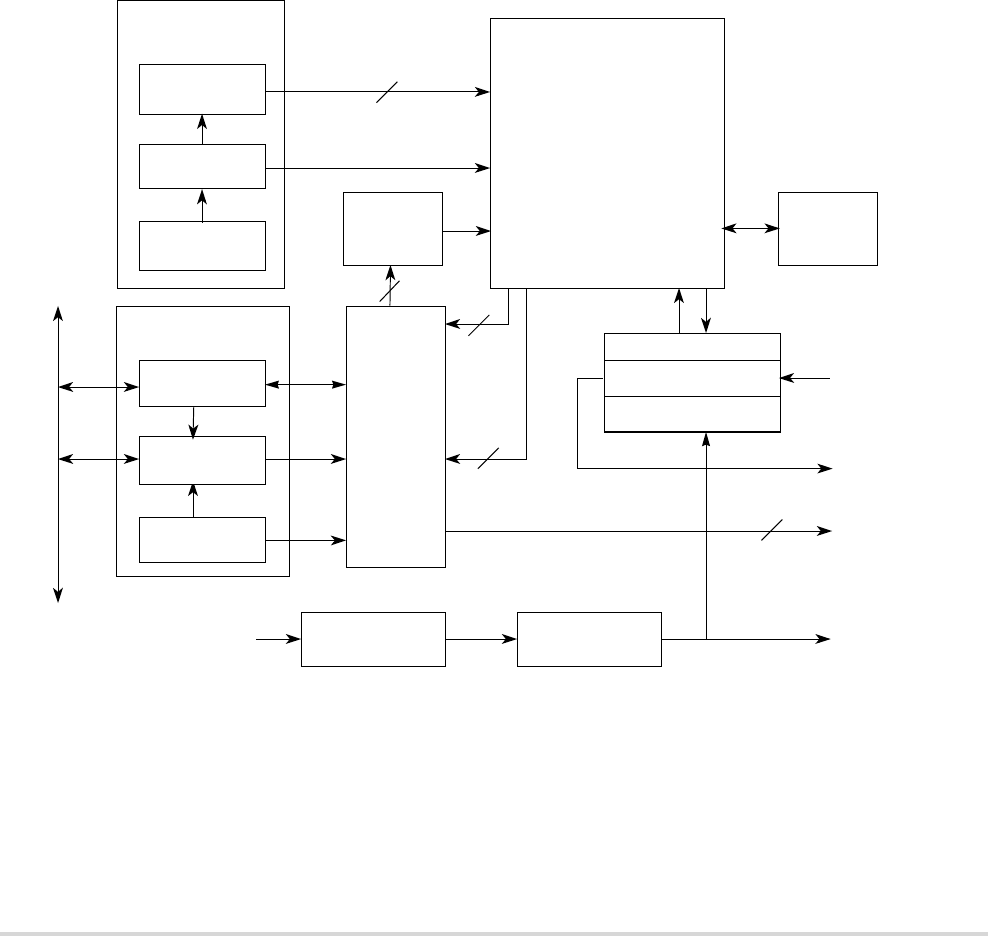
22-2 MCF5282 User’s Manual MOTOROLA
Module Description
22.3.1 Interface and Signals
The module provides access to as many as 15 devices with a total of seven signals:
QSPI_Dout, QSPI_Din, QSPI_CLK, QSPI_CS0, QSPI_CS1, QSPI_CS2, and QSPI_CS3.
Peripheral chip-select signals, QSPI_CS[3:0], are used to select an external device as the
source or destination for serial data transfer. Signals are asserted at a logic level
corresponding to the value of the QSPI_CS[3:0] bits in the command RAM whenever a
command in the queue is executed. More than one chip-select signal can be asserted
simultaneously.
Although QSPI_CS[3:0] will function as simple chip selects in most applications, up to 15
devices can be selected by decoding them with an external 4-to-16 decoder.
Figure 22-1. QSPI Block Diagram
Queue Control
Block
Queue
Pointer
System Clock
4
Done
Comparator
End Queue
Pointer
Status
Regs
Delay
Counter
Control Logic
Control
Regs
80-Byte
QSPI
RAM
Chip
Select
Command
Divide by 2 Baud Rate
Generator
msb lsb
Logic
Array
QSPI_CLK
QSPI_CS[3:0]
QSPI_Din
8
/16 Bit Shift Reg
.
Rx/Tx Data Reg.
QSPI_Dout
4
4
4
Internal Bus
4
QSPI
Address
Register
QSPI
Data
Register

MOTOROLA Chapter 22. Queued Serial Peripheral Interface (QSPI) Module 22-3
Operation
22.3.2 Internal Bus Interface
Because the QSPI module only operates in master mode, the master bit in the QSPI mode
register, QMR[MSTR], must be set for the QSPI to function properly. The QSPI can initiate
serial transfers but cannot respond to transfers initiated by other QSPI masters.
22.4 Operation
The QSPI uses a dedicated 80-Byte block of static RAM accessible both to the module and
the CPU to perform queued operations. The RAM is divided into three segments as follows:
• 16 command control bytes (command RAM)
• 16 transmit data words (transfer RAM)
• 16 receive data words (transfer RAM)
The RAM is organized so that 1 byte of command control data, 1 word of transmit data, and
1 word of receive data comprise 1 of the 16 queue entries (0x0–0xF).
NOTE
Throughout ColdFire documentation, “word” is used
consistently and exclusively to designate a 16-bit data unit. The
only exceptions to this appear in discussions of serial
communication modules such as QSPI that support
variable-length data units. To simplify these discussions the
functional unit is referred to as a ‘word’ regardless of length.
The user initiates QSPI operation by loading a queue of commands in command RAM,
writing transmit data into transmit RAM, and then enabling the QSPI data transfer. The
QSPI executes the queued commands and sets the completion flag in the QSPI interrupt
register (QIR[SPIF]) to signal their completion. As another option, QIR[SPIFE] can be
enabled to generate an interrupt.
The QSPI uses four queue pointers. The user can access three of them through fields in
QSPI wrap register (QWR):
• The new queue pointer, QWR[NEWQP], points to the first command in the queue.
• An internal queue pointer points to the command currently being executed.
Table 22-1. QSPI Input and Output Signals and Functions
Signal Name Hi-Z or Actively Driven Function
QSPI Data Output (QSPI_Dout) Configurable Serial data output from QSPI
QSPI Data Input (QSPI_Din) N/A Serial data input to QSPI
Serial Clock (QSPI_CLK) Actively driven Clock output from QSPI
Peripheral Chip Selects (QSPI_CS[3:0]) Actively driven Peripheral selects

22-4 MCF5282 User’s Manual MOTOROLA
Operation
• The completed queue pointer, QWR[CPTQP], points to the last command executed.
• The end queue pointer, QWR[ENDQP], points to the final command in the queue.
The internal pointer is initialized to the same value as QWR[NEWQP]. During normal
operation, the following sequence repeats:
1. The command pointed to by the internal pointer is executed.
2. The value in the internal pointer is copied into QWR[CPTQP].
3. The internal pointer is incremented.
Execution continues at the internal pointer address unless the QWR[NEWQP] value is
changed. After each command is executed, QWR[ENDQP] and QWR[CPTQP] are
compared. When a match occurs, QIR[SPIF] is set and the QSPI stops unless wraparound
mode is enabled. Setting QWR[WREN] enables wraparound mode.
QWR[NEWQP] is cleared at reset. When the QSPI is enabled, execution begins at address
0x0 unless another value has been written into QWR[NEWQP]. QWR[ENDQP] is cleared
at reset but is changed to show the last queue entry before the QSPI is enabled.
QWR[NEWQP] and QWR[ENDQP] can be written at any time. When the QWR[NEWQP]
value changes, the internal pointer value also changes unless a transfer is in progress, in
which case the transfer completes normally. Leaving QWR[NEWQP] and QWR[ENDQP]
set to 0x0 causes a single transfer to occur when the QSPI is enabled.
Data is transferred relative to QSPI_CLK which can be generated in any one of four
combinations of phase and polarity using QMR[CPHA,CPOL]. Data is transferred with the
most significant bit (msb) first. The number of bits transferred defaults to 8, but can be set
to any value between 8 and 16 by writing a value into the BITSE field of the command
RAM (QCR[BITSE]).
22.4.1 QSPI RAM
The QSPI contains an 80-Byte block of static RAM that can be accessed by both the user
and the QSPI. This RAM does not appear in the MCF5282 memory map because it can only
be accessed by the user indirectly through the QSPI address register (QAR) and the QSPI
data register (QDR). The RAM is divided into three segments with 16 addresses each:
• Receive data RAM, the initial destination for all incoming data
• Transmit data RAM, a buffer for all out-bound data
• Command RAM, where commands are loaded
The transmit and command RAM are user write-only. The receive RAM is user read-only.
Figure 22-2 shows the RAM configuration. The RAM contents are undefined immediately
after a reset.
The command and data RAM in the QSPI is indirectly accessible with QDR and QAR as
48 separate locations that comprise 16 words of transmit data, 16 words of receive data and

MOTOROLA Chapter 22. Queued Serial Peripheral Interface (QSPI) Module 22-5
Operation
16 bytes of commands.
A write to QDR causes data to be written to the RAM entry specified by QAR[ADDR] and
causes the value in QAR to increment. Correspondingly, a read at QDR returns the data in
the RAM at the address specified by QAR[ADDR]. This also causes QAR to increment. A
read access requires a single wait state.
22.4.1.1 Receive RAM
Data received by the QSPI is stored in the receive RAM segment located at 0x10 to 0x1F
in the QSPI RAM space. The user reads this segment to retrieve data from the QSPI. Data
words with less than 16 bits are stored in the least significant bits of the RAM. Unused bits
in a receive queue entry are set to zero upon completion of the individual queue entry.
QWR[CPTQP] shows which queue entries have been executed. The user can query this
field to determine which locations in receive RAM contain valid data.
Relative Address Register Function
0x00 QTR0 Transmit RAM
0x01 QTR1
..16 bits wide
..
..
0x0F QTR15
0x10 QRR0 Receive RAM
0x11 QRR1
..16 bits wide
..
..
0x1F QRR15
0x20 QCR0 Command RAM
0x21 QCR1
..8 bits wide
..
..
0x2F QCR15
Figure 22-2. QSPI RAM Model

22-6 MCF5282 User’s Manual MOTOROLA
Operation
22.4.1.2 Transmit RAM
Data to be transmitted by the QSPI is stored in the transmit RAM segment located at
addresses 0x0 to 0xF. The user normally writes 1 word into this segment for each queue
command to be executed. The user cannot read data in the transmit RAM.
Out-bound data must be written to transmit RAM in a right-justified format. The unused
bits are ignored. The QSPI copies the data to its data serializer (shift register) for
transmission. The data is transmitted most significant bit first and remains in transmit RAM
until overwritten by the user.
22.4.1.3 Command RAM
The CPU writes one byte of control information to this segment for each QSPI command
to be executed. Command RAM, referred to as QCR0–15, is write-only memory from a
user’s perspective.
Command RAM consists of 16 bytes with each byte divided into two fields. The peripheral
chip select field controls the QSPI_CS signal levels for the transfer. The command control
field provides transfer options.
A maximum of 16 commands can be in the queue. Queue execution proceeds from the
address in QWR[NEWQP] through the address in QWR[ENDQP].
The QSPI executes a queue of commands defined by the control bits in each command
RAM entry which sequence the following actions:
• Chip-select pins are activated
• Data is transmitted from transmit RAM and received into the receive RAM
• The synchronous transfer clock QSPI_CLK is generated
Before any data transfers begin, control data must be written to the command RAM, and
any out-bound data must be written to transmit RAM. Also, the queue pointers must be
initialized to the first and last entries in the command queue.
Data transfer is synchronized with the internally generated QSPI_CLK, whose phase and
polarity are controlled by QMR[CPHA] and QMR[CPOL]. These control bits determine
which QSPI_CLK edge is used to drive outgoing data and to latch incoming data.
22.4.2 Baud Rate Selection
The maximum QSPI clock frequency is one-fourth the clock frequency of the system clock.
Baud rate is selected by writing a value from 2–255 into QMR[BAUD]. The QSPI uses a
prescaler to derive the QSPI_CLK rate from the system clock divided by two.
A baud rate value of zero turns off the QSPI_CLK.

MOTOROLA Chapter 22. Queued Serial Peripheral Interface (QSPI) Module 22-7
Operation
The desired QSPI_CLK baud rate is related to the system clock and QMR[BAUD] by the
following expression:
QMR[BAUD] = fSYS / [2 ×(desired QSPI_CLK baud rate)]
22.4.3 Transfer Delays
The QSPI supports programmable delays for the QSPI_CS signals before and after a
transfer. The time between QSPI_CS assertion and the leading QSPI_CLK edge, and the
time between the end of one transfer and the beginning of the next, are both independently
programmable.
The chip select to clock delay enable bit in command RAM, QCR[DSCK], enables the
programmable delay period from QSPI_CS assertion until the leading edge of QSPI_CLK.
QDLYR[QCD] determines the period of delay before the leading edge of QSPI_CLK. The
following expression determines the actual delay before the QSPI_CLK leading edge:
QSPI_CS-to-QSPI_CLK delay = QDLYR[QCD]/fSYS
QDLYR[QCD] has a range of 1–127.
When QDLYR[QCD] or QCR[DSCK] equals zero, the standard delay of one-half the
QSPI_CLK period is used.
The command RAM delay after transmit enable bit, QCR[DT], enables the programmable
delay period from the negation of the QSPI_CS signals until the start of the next transfer.
The delay after transfer can be used to provide a peripheral deselect interval. A delay can
also be inserted between consecutive transfers to allow serial A/D converters to complete
conversion. There are two transfer delay options: the user can choose to delay a standard
period after serial transfer is complete or can specify a delay period. Writing a value to
QDLYR[DTL] specifies a delay period. QCR[DT] determines whether the standard delay
period (DT = 0) or the specified delay period (DT = 1) is used. The following expression is
used to calculate the delay:
Table 22-2. QSPI_CLK Frequency as Function of System Clock and Baud Rate
System Clock
QMR [BAUD] 66.67 MHz
2 16.5 MHz
4 8.25 MHz
8 4.125 MHz
16 2.063 MHz
32 1.031 MHz
255 129.4 kHz

22-8 MCF5282 User’s Manual MOTOROLA
Operation
Delay after transfer = 32 ×QDLYR[DTL] /fSYS (DT = 1)
where QDLYR[DTL] has a range of 1–255.
A zero value for DTL causes a delay-after-transfer value of 8192/fSYS.
Standard delay after transfer = 17/fSYS (DT = 0)
Adequate delay between transfers must be specified for long data streams because the QSPI
module requires time to load a transmit RAM entry for transfer. Receiving devices need at
least the standard delay between successive transfers. If the system clock is operating at a
slower rate, the delay between transfers must be increased proportionately.
22.4.4 Transfer Length
There are two transfer length options. The user can choose a default value of 8 bits or a
programmed value of 8 to 16 bits. The programmed value must be written into
QMR[BITS]. The command RAM bits per transfer enable field, QCR[BITSE], determines
whether the default value (BITSE = 0) or the BITS[3–0] value (BITSE = 1) is used.
QMR[BITS] gives the required number of bits to be transferred, with 0b0000 representing
16.
22.4.5 Data Transfer
Operation is initiated by setting QDLYR[SPE]. Shortly after QDLYR[SPE] is set, the QSPI
executes the command at the command RAM address pointed to by QWR[NEWQP]. Data
at the pointer address in transmit RAM is loaded into the data serializer and transmitted.
Data that is simultaneously received is stored at the pointer address in receive RAM.
When the proper number of bits has been transferred, the QSPI stores the working queue
pointer value in QWR[CPTQP], increments the working queue pointer, and loads the next
data for transfer from the transmit RAM. The command pointed to by the incremented
working queue pointer is executed next unless a new value has been written to
QWR[NEWQP]. If a new queue pointer value is written while a transfer is in progress, then
that transfer is completed normally.
When the CONT bit in the command RAM is set, the QSPI_CS signals are asserted
between transfers. When CONT is cleared, QSPI_CS[3:0] are negated between transfers.
The QSPI_CS signals are not high impedance.
When the QSPI reaches the end of the queue, it asserts the SPIF flag, QIR[SPIF]. If
QIR[SPIFE] is set, an interrupt request is generated when QIR[SPIF] is asserted. Then the
QSPI clears QDLYR[SPE] and stops, unless wraparound mode is enabled.
Wraparound mode is enabled by setting QWR[WREN]. The queue can wrap to pointer
address 0x0, or to the address specified by QWR[NEWQP], depending on the state of
QWR[WRTO].

MOTOROLA Chapter 22. Queued Serial Peripheral Interface (QSPI) Module 22-9
Programming Model
In wraparound mode, the QSPI cycles through the queue continuously, even while
requesting interrupt service. QDLYR[SPE] is not cleared when the last command in the
queue is executed. New receive data overwrites previously received data in the receive
RAM. Each time the end of the queue is reached, QIR[SPIFE] is set. QIR[SPIF] is not
automatically reset. If interrupt driven QSPI service is used, the service routine must clear
QIR[SPIF] to abort the current request. Additional interrupt requests during servicing can
be prevented by clearing QIR[SPIFE].
There are two recommended methods of exiting wraparound mode: clearing QWR[WREN]
or setting QWR[HALT]. Exiting wraparound mode by clearing QDLYR[SPE] is not
recommended because this may abort a serial transfer in progress. The QSPI sets SPIF,
clears QDLYR[SPE], and stops the first time it reaches the end of the queue after
QWR[WREN] is cleared. After QWR[HALT] is set, the QSPI finishes the current transfer,
then stops executing commands. After the QSPI stops, QDLYR[SPE] can be cleared.
22.5 Programming Model
Table 22-3 is the QSPI register memory map. Reading reserved locations returns zeros.
The programming model for the QSPI consists of six registers. They are the QSPI mode
register (QMR), QSPI delay register (QDLYR), QSPI wrap register (QWR), QSPI interrupt
register (QIR), QSPI address register (QAR), and the QSPI data register (QDR).
There are a total of 80 bytes of memory used for transmit, receive, and control data. This
memory is accessed indirectly using QAR and QDR.
Registers and RAM are written and read by the CPU.
Table 22-3. QSPI Registers
IPSBAR
Offset [31:24] [23:16] [15:8] [7:0]
0x340 QSPI Mode Register (QMR) [p. 22-10] Reserved 1
1Addresses not assigned to a register and undefined register bits are reserved for expansion. Write accesses to these reserved
address spaces and reserved register bits have no effect.
0x344 QSPI Delay Register (QDLYR) [p. 22-11] Reserved1
0x348 QSPI Wrap Register (QWR) [p. 22-12] Reserved1
0x34C QSPI Interrupt Register (QIR) [p. 22-13] Reserved1
0x350 QSPI Address Register (QAR) [p. 22-14] Reserved1
0x354 QSPI Data Register (QDR) [p. 22-14] Reserved1

22-10 MCF5282 User’s Manual MOTOROLA
Programming Model
22.5.1 QSPI Mode Register (QMR)
The QMR, shown in Figure 22-3, determines the basic operating modes of the QSPI
module. Parameters such as QSPI_CLK polarity and phase, baud rate, master mode
operation, and transfer size are determined by this register. The data output high impedance
enable, DOHIE, controls the operation of QSPI_Dout between data transfers. When
DOHIE is cleared, QSPI_Dout is actively driven between transfers. When DOHIE is set,
QSPI_Dout assumes a high impedance state.
NOTE
Because the QSPI does not operate in slave mode, the master
mode enable bit, QMR[MSTR], must be set for the QSPI
module to operate correctly.
Table 22-4 gives QMR field descriptions.
15 14 13 10 9 8 7 0
Field MSTR DOHIE BITS CPOL CPHA BAUD
Reset 0000_0001_0000_0100
R/W R/W
Address IPSBAR + 0x340
Figure 22-3. QSPI Mode Register (QMR)
Table 22-4. QMR Field Descriptions
Bits Name Description
15 MSTR Master mode enable.
0 Reserved, do not use.
1 The QSPI is in master mode. Must be set for the QSPI module to operate correctly.
14 DOHIE Data output high impedance enable. Selects QSPI_Dout mode of operation.
0 Default value after reset. QSPI_Dout is actively driven between transfers.
1 QSPI_Dout is high impedance between transfers.
13–10 BITS Transfer size. Determines the number of bits to be transferred for each entry in the queue.
Value Bits per transfer
0000 16
0001– 0111 Reserved
1000 8
1001 9
1010 10
1011 11
1100 12
1101 13
1110 14
1111 15
9 CPOL Clock polarity. Defines the clock polarity of QSPI_CLK.
0 The inactive state value of QSPI_CLK is logic level 0.
1 The inactive state value of QSPI_CLK is logic level 1.
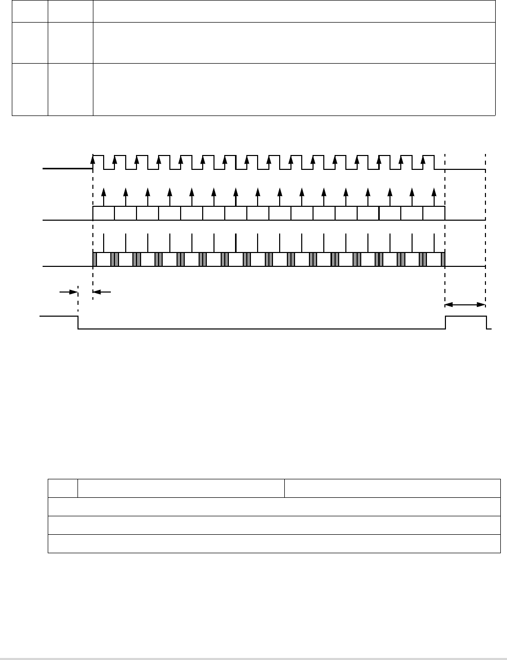
MOTOROLA Chapter 22. Queued Serial Peripheral Interface (QSPI) Module 22-11
Programming Model
Figure 22-4 shows an example of a QSPI clocking and data transfer.
Figure 22-4. QSPI Clocking and Data Transfer Example
22.5.2 QSPI Delay Register (QDLYR)
Figure 22-5 shows the QDLYR.
8 CPHA Clock phase. Defines the QSPI_CLK clock-phase.
0 Data captured on the leading edge of QSPI_CLK and changed on the following edge of QSPI_CLK.
1 Data changed on the leading edge of QSPI_CLK and captured on the following edge of QSPI_CLK.
7–0 BAUD Baud rate divider. The baud rate is selected by writing a value in the range 2–255. A value of zero disables
the QSPI. A value of 1 is an invalid setting. The desired QSPI_CLK baud rate is related to the system clock
and QMR[BAUD] by the following expression:
QMR[BAUD] = fSYS / [2 ×(desired QSPI_CLK baud rate)]
15 14 8 7 0
Field SPE QCD DTL
Reset 0000_0100_0000_0100
R/W R/W
Address IPSBAR + 0x344
Figure 22-5. QSPI Delay Register (QDLYR)
Table 22-4. QMR Field Descriptions (continued)
Bits Name Description
QSPI_CLK
QSPI_Dout
QSPI_Din
QSPI_CS
AB
QMR[CPOL] = 0
QMR[CPHA] = 1
QCR[CONT] = 0
Chip selects are active low
A = QDLYR[QCD]
B = QDLYR[DTL]
15 14 13 12 11 10 9 8 7 6 5 4 3 2 1 0
15 14 13 12 11 10 9 8 7 6 5 4 3 2 1 0
msb

22-12 MCF5282 User’s Manual MOTOROLA
Programming Model
Table 22-5 gives QDLYR field descriptions.
22.5.3 QSPI Wrap Register (QWR)
Table 22-6 gives QWR field descriptions.
Table 22-5. QDLYR Field Descriptions
Bits Name Description
15 SPE QSPI enable. When set, the QSPI initiates transfers in master mode by executing commands in the command
RAM. Automatically cleared by the QSPI when a transfer completes. The user can also clear this bit to abort
transfer unless QIR[ABRTL] is set. The recommended method for aborting transfers is to set QWR[HALT].
14–8 QCD QSPICLK delay. When the DSCK bit in the command RAM is set this field determines the length of the delay
from assertion of the chip selects to valid QSPI_CLK transition.
7–0 DTL Delay after transfer. When the DT bit in the command RAM is set this field determines the length of delay
after the serial transfer.
15 14 13 12 11 8 7 4 3 0
Field HALT WREN WRTO CSIV ENDQP CPTQP NEWQP
Reset 0000_0000_0000_0000
R/W R/W R R/W
Address IPSBAR + 0x348
Figure 22-6. QSPI Wrap Register (QWR)
Table 22-6. QWR Field Descriptions
Bits Name Description
15 HALT Halt transfers. Assertion of this bit causes the QSPI to stop execution of commands once it has completed
execution of the current command.
14 WREN Wraparound enable. Enables wraparound mode.
0 Execution stops after executing the command pointed to by QWR[ENDQP].
1 After executing command pointed to by QWR[ENDQP], wrap back to entry zero, or the entry pointed
to by QWR[NEWQP] and continue execution.
13 WRTO Wraparound location. Determines where the QSPI wraps to in wraparound mode.
0 Wrap to RAM entry zero.
1 Wrap to RAM entry pointed to by QWR[NEWQP].
12 CSIV QSPI_CS inactive level.
0 QSPI chip select outputs return to zero when not driven from the value in the current command RAM
entry during a transfer (that is, inactive state is 0, chip selects are active high).
1 QSPI chip select outputs return to one when not driven from the value in the current command RAM
entry during a transfer (that is, inactive state is 1, chip selects are active low).
11–8 ENDQP End of queue pointer. Points to the RAM entry that contains the last transfer description in the queue.
7–4 CPTQP Completed queue entry pointer. Points to the RAM entry that contains the last command to have been
completed. This field is read only.
3–0 NEWQP Start of queue pointer. This 4-bit field points to the first entry in the RAM to be executed on initiating a
transfer.

MOTOROLA Chapter 22. Queued Serial Peripheral Interface (QSPI) Module 22-13
Programming Model
22.5.4 QSPI Interrupt Register (QIR)
Figure 22-7 shows the QIR register.
Table 22-7 describes QIR fields.
15 14 13 12 11 10 9 8 7 4 3 2 1 0
Field WCEFB ABRTB — ABRT
L
WCEFE ABRTE — SPIFE — WCEF ABRT — SPIF
Reset 0000_0000_0000_0000
R/W R/W
Address IPSBAR + 0x34C
Figure 22-7. QSPI Interrupt Register (QIR)
Table 22-7. QIR Field Descriptions
BIts Name Description
15 WCEFB Write collision access error enable. A write collision occurs during a data transfer when the RAM
entry containing the command currently being executed is written to by the CPU with the QDR.
When this bit is asserted, the write access to QDR results in an access error.
14 ABRTB Abort access error enable. An abort occurs when QDLYR[SPE] is cleared during a transfer. When
set, an attempt to clear QDLYR[SPE] during a transfer results in an access error.
13 — Reserved, should be cleared.
12 ABRTL Abort lock-out. When set, QDLYR[SPE] cannot be cleared by writing to the QDLYR. QDLYR[SPE]
is only cleared by the QSPI when a transfer completes.
11 WCEFE Write collision interrupt enable. Interrupt enable for WCEF. Setting this bit enables the interrupt, and
clearing it disables the interrupt.
10 ABRTE Abort interrupt enable. Interrupt enable for ABRT flag. Setting this bit enables the interrupt, and
clearing it disables the interrupt.
9 — Reserved, should be cleared.
8 SPIFE QSPI finished interrupt enable. Interrupt enable for SPIF. Setting this bit enables the interrupt, and
clearing it disables the interrupt.
7–4 — Reserved, should be cleared.
3 WCEF Write collision error flag. Indicates that an attempt has been made to write to the RAM entry that is
currently being executed. Writing a 1 to this bit clears it and writing 0 has no effect.
2 ABRT Abort flag. Indicates that QDLYR[SPE] has been cleared by the user writing to the QDLYR rather
than by completion of the command queue by the QSPI. Writing a 1 to this bit clears it and writing
0 has no effect.
1 — Reserved, should be cleared.
0 SPIF QSPI finished flag. Asserted when the QSPI has completed all the commands in the queue. Set on
completion of the command pointed to by QWR[ENDQP], and on completion of the current
command after assertion of QWR[HALT]. In wraparound mode, this bit is set every time the
command pointed to by QWR[ENDQP] is completed. Writing a 1 to this bit clears it and writing 0
has no effect.

22-14 MCF5282 User’s Manual MOTOROLA
Programming Model
The command and data RAM in the QSPI are indirectly accessible with QDR and QAR as
48 separate locations that comprise 16 words of transmit data, 16 words of receive data, and
16 bytes of commands.
A write to QDR causes data to be written to the RAM entry specified by QAR[ADDR].
This also causes the value in QAR to increment.
Correspondingly, a read at QDR returns the data in the RAM at the address specified by
QAR[ADDR]. This also causes QAR to increment. A read access requires a single wait
state.
NOTE
The QAR does not wrap after the last queue entry within each
section of the RAM. The application software must handle
address range errors.
22.5.5 QSPI Address Register (QAR)
The QAR, shown in Figure 22-8, is used to specify the location in the QSPI RAM that read
and write operations affect.
22.5.6 QSPI Data Register (QDR)
The QDR, shown in Figure 22-9, is used to access QSPI RAM indirectly. The CPU reads
and writes all data from and to the QSPI RAM through this register.
15 65 0
Field — ADDR
Reset 0000_0000_0000_0000
R/W R/W
Address IPSBAR + 0x350
Figure 22-8. QSPI Address Register
15 0
Field DATA
Reset 0000_0000_0000_0000
R/W R/W
Address IPSBAR + 0x354
Figure 22-9. QSPI Data Register (QDR)

MOTOROLA Chapter 22. Queued Serial Peripheral Interface (QSPI) Module 22-15
Programming Model
22.5.7 Command RAM Registers (QCR0–QCR15)
The command RAM is accessed using the upper byte of QDR. The QSPI cannot modify
information in command RAM.
There are 16 bytes in the command RAM. Each byte is divided into two fields. The chip
select field enables external peripherals for transfer. The command field provides transfer
operations.
NOTE
The command RAM is accessed only using the most
significant byte of QDR and indirect addressing based on
QAR[ADDR].
Figure 22-10 shows the command RAM register.
Table 22-8 gives QCR field descriptions.
15 14 13 12 11 8 7 0
Field CONT BITSE DT DSCK QSPI_CS –
Reset Undefined
R/W Write Only
Address QAR[ADDR]
Figure 22-10. Command RAM Registers (QCR0–QCR15)
Table 22-8. QCR0–QCR15 Field Descriptions
Bits Name Description
15 CONT Continuous.
0 Chip selects return to inactive level defined by QWR[CSIV] when transfer is complete.
1 Chip selects remain asserted after the transfer of 16 words of data (see note below).
14 BITSE Bits per transfer enable.
0 Eight bits
1 Number of bits set in QMR[BITS]
13 DT Delay after transfer enable.
0 Default reset value.
1 The QSPI provides a variable delay at the end of serial transfer to facilitate interfacing with
peripherals that have a latency requirement. The delay between transfers is determined by
QDLYR[DTL].
12 DSCK Chip select to QSPI_CLK delay enable.
0 Chip select valid to QSPI_CLK transition is one-half QSPI_CLK period.
1 QDLYR[QCD] specifies the delay from QSPI_CS valid to QSPI_CLK.
11–8 QSPI_CS Peripheral chip selects. Used to select an external device for serial data transfer. More than one chip
select may be active at once, and more than one device can be connected to each chip select. Bits
11–8 map directly to QSPI_CS[3:0], respectively. If it is desired to use those bits as a chip select
value, then an external demultiplexor must be connected to the QSPI_CS[3:0] pins.
7–0 — Reserved, should be cleared.
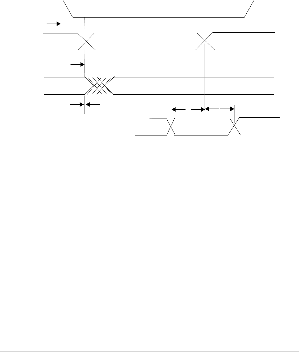
22-16 MCF5282 User’s Manual MOTOROLA
Programming Model
NOTE
In order to keep the chip selects asserted for all transfers, the
QWR[CSIV] bit must be set to control the level that the chip
selects return to after the first transfer.
Figure 22-11. QSPI Timing
22.5.8 Programming Example
The following steps are necessary to set up the QSPI 12-bit data transfers and a QSPI_CLK
of 4.125 MHz. The QSPI RAM is set up for a queue of 16 transfers. All four QSPI_CS
signals are used in this example.
1. Write the QMR with 0xB308 to set up 12-bit data words with the data shifted on the
falling clock edge, and a QSPI_CLK frequency of 4.125 MHz (assuming a 66-MHz
system clock).
2. Write QDLYR with the desired delays.
QSPICS[3:0]
QSPI_CLK
QSPI_DOUT
QSPI_DIN
QS1
QS1: QSPICS to QSPI_CLK
QS2: QSPI_CLK to QSPI_DOUT VALID
QS3: QSPI_CLK to QSPI_DOUT HOLD
QS4: QSPI_DIN to QSPI_CLK SETUP
QS2
QS3 QS4 QS5
QS5: QSPI_DIN to QSPI_CLK HOLD
1T1
0 ns
10 ns
10 ns
Min Max
20 ns
1 T1 is defined as the clock period in ns.

MOTOROLA Chapter 22. Queued Serial Peripheral Interface (QSPI) Module 22-17
Programming Model
3. Write QIR with 0xD00F to enable write collision, abort bus errors, and clear any
interrupts.
4. Write QAR with 0x0020 to select the first command RAM entry.
5. Write QDR with 0x7E00, 0x7E00, 0x7E00, 0x7E00, 0x7D00, 0x7D00, 0x7D00,
0x7D00, 0x7B00, 0x7B00, 0x7B00, 0x7B00, 0x7700, 0x7700, 0x7700, and
0x7700 to set up four transfers for each chip select. The chip selects are active low
in this example.
6. Write QAR with 0x0000 to select the first transmit RAM entry.
7. Write QDR with sixteen 12-bit words of data.
8. Write QWR with 0x0F00 to set up a queue beginning at entry 0 and ending at entry
15.
9. Set QDLYR[SPE] to enable the transfers.
10. Wait until the transfers are complete. QIR[SPIF] is set when the transfers are
complete.
11. Write QAR with 0x0010 to select the first receive RAM entry.
12. Read QDR to get the received data for each transfer.
13. Repeat steps 5 through 13 to do another transfer.

22-18 MCF5282 User’s Manual MOTOROLA
Programming Model
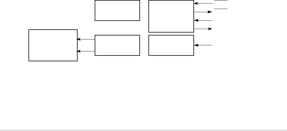
MOTOROLA Chapter 23. UART Modules 23-1
Chapter 23
UART Modules
This chapter describes the use of the universal asynchronous receiver/transmitters (UARTs)
implemented on the MCF5282 and includes programming examples.
NOTE
The designation “n” is used throughout this section to refer to
registers or signals associated with one of the three identical
UART modules: UART0, UART1, or UART2.
23.1 Overview
The MCF5282 contains three independent UARTs. Each UART can be clocked by the
system clock, eliminating the need for an external UART clock. As Figure 23-1 shows,
each UART module interfaces directly to the CPU and consists of the following:
• Serial communication channel
• Programmable clock generation
• Internal channel control logic
• Interrupt control logic
Figure 23-1. Simplified Block Diagram
NOTE
UART0 can be clocked by the DTIN0 pin. UART1 can be
clocked by the DTIN1 pin, and UART2 can be clocked by
DTIN2.
Serial
Interrupt Control
Logic
UCTS
URTS
URXD
UTXD
or
External clock (DTINn)
Internal Channel
Control Logic
Programmable
Clock
Communications
Channel
Generation
System Control
Module (SCM)
Interrupt
Controller
UART
System Clock

23-2 MCF5282 User’s Manual MOTOROLA
Serial Module Overview
The serial communication channel provides a full-duplex asynchronous/synchronous
receiver and transmitter deriving an operating frequency from the system clock or an
external clock using the timer pin. The transmitter converts parallel data from the CPU to
a serial bit stream, inserting appropriate start, stop, and parity bits. It outputs the resulting
stream on the channel transmitter serial data output (UTXDn). See Section 23.5.2.1,
“Transmitter.”
The receiver converts serial data from the channel receiver serial data input (URXDn) to
parallel format, checks for a start, stop, and parity bits, or break conditions, and transfers
the assembled character onto the bus during read operations. The receiver may be polled,
interrupt driven, or use DMA requests for servicing. See Section 23.5.2.2, “Receiver.”
23.2 Serial Module Overview
The MCF5282 contains three independent UART modules, whose features are as follows:
• Each can be clocked by the system clock, eliminating a need for an external
UART clock
• Full-duplex asynchronous/synchronous receiver/transmitter channel
• Quadruple-buffered receiver
• Double-buffered transmitter
• Independently programmable receiver and transmitter clock sources
• Programmable data format:
— 5–8 data bits plus parity
— Odd, even, no parity, or force parity
— One, one-and-a-half, or two stop bits
• Each channel programmable to normal (full-duplex), automatic echo, local
loop-back, or remote loop-back mode
• Automatic wake-up mode for multidrop applications
• Four maskable interrupt conditions
• All three UARTs have DMA request capability
• Parity, framing, and overrun error detection
• False-start bit detection
• Line-break detection and generation
• Detection of breaks originating in the middle of a character
• Start/end break interrupt/status

MOTOROLA Chapter 23. UART Modules 23-3
Register Descriptions
23.3 Register Descriptions
This section contains a detailed description of each register and its specific function.
Flowcharts in Section 23.5.6, “Programming,” describe basic UART module
programming. The operation of the UART module is controlled by writing control bytes
into the appropriate registers. Table 23-1 is a memory map for UART module registers.
Table 23-1. UART Module Memory Map
IPSBAR Offset
[31:24] [23:16] [15:8] [7:0]
UART0 UART1 UART2
0x200 0x240 0x280 UART mode registers 1—(UMR1n) [p. 23-4],
(UMR2n) [p. 23-6]
—
0x204 0x244 0x284 (Read) UART status registers—(USRn) [p. 23-7] —
(Write) UART clock select register1—(UCSRn)
[p. 23-8]
—
0x208 0x248 0x288 (Read) Do not access 2 —
(Write) UART command registers—(UCRn)
[p. 23-9]
—
0x20C 0x24C 0x28C (UART/Read) UART receive buffers—(URBn)
[p. 23-11]
—
(UART/Write) UART transmit buffers—(UTBn)
[p. 23-11]
—
0x210 0x250 0x290 (Read) UART input port change
registers—(UIPCRn) [p. 23-12]
—
(Write) UART auxiliary control
registers1—(UACRn) [p. 23-13]
—
0x214 0x254 0x294 (Read) UART interrupt status registers—(UISRn)
[p. 23-13]
—
(Write) UART interrupt mask
registers—(UIMRn) [p. 23-13]
—
0x218 0x258 0x298 (Read) Do not access2—
UART divider upper registers—(UBG1n)
[p. 23-14]
—
0x21C 0x25C 0x29C (Read) Do not access2—
UART divider lower registers—(UBG2n)
[p. 23-14]
—
0x234 0x274 0x2B4 (Read) UART input port registers—(UIPn)
[p. 23-15]
—
(Write) Do not access2—
0x238 0x278 0x2B8 (Read) Do not access2—
(Write) UART output port bit set command
registers—(UOP1n 3) [p. 23-15]
—

23-4 MCF5282 User’s Manual MOTOROLA
Register Descriptions
NOTE
UART registers are accessible only as bytes.
NOTE
Interrupt can mean either an interrupt request asserted to the
CPU or a DMA request.
23.3.1 UART Mode Registers 1 (UMR1n)
The UMR1n registers control configuration. UMR1n can be read or written when the mode
register pointer points to it, at RESET or after a RESET MODE REGISTER POINTER command
using UCRn[MISC]. After UMR1n is read or written, the pointer points to UMR2n.
0x23C 0x27C 0x2BC (Read) Do not access2—
(Write) UART output port bit reset command
registers—(UOP0n3) [p. 23-15]
—
1UMR1n, UMR2n, and UCSRn should be changed only after the receiver/transmitter is issued a software reset command. That is,
if channel operation is not disabled, undesirable results may occur.
2This address is for factory testing. Reading this location results in undesired effects and possible incorrect transmission or
reception of characters. Register contents may also be changed.
3Address-triggered commands
7 6 543210
Field RxRTS RxIRQ/FFULL ERR PM PT B/C
Reset 0000_0000
R/W R/W
Address IPSBAR + 0x200 (UART0), 0x240 (UART1), 0x280 (UART2). After UMR1n is read or written, the pointer points to
UMR2n.
Figure 23-2. UART Mode Registers 1 (UMR1n)
Table 23-1. UART Module Memory Map (continued)
IPSBAR Offset
[31:24] [23:16] [15:8] [7:0]
UART0 UART1 UART2
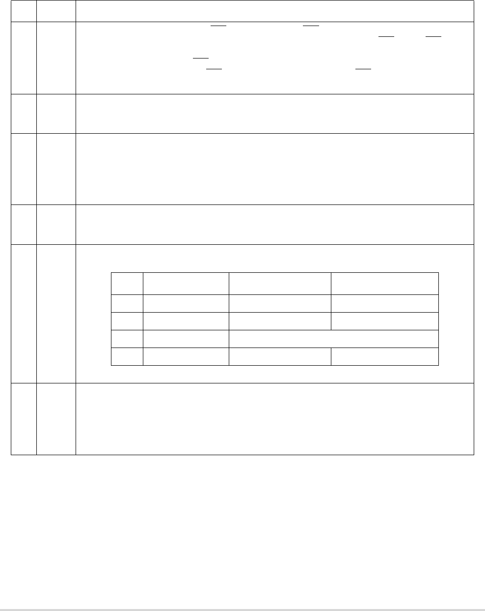
MOTOROLA Chapter 23. UART Modules 23-5
Register Descriptions
Table 23-2 describes UMR1n fields.
Table 23-2. UMR1n Field Descriptions
Bits Name Description
7 RxRTS Receiver request-to-send. Allows the RTS output to control the CTS input of the transmitting device to prevent
receiver overrun. If both the receiver and transmitter are incorrectly programmed for RTS control, RTS control
is disabled for both. Transmitter RTS control is configured in UMR2n[TxRTS].
0 The receiver has no effect on RTS.
1 When a valid start bit is received, RTS is negated if the UART's FIFO is full. RTS is reasserted when the FIFO
has an empty position available.
6 RxIRQ/
FFULL
Receiver interrupt select.
0 RxRDY is the source that generates IRQ or DMA request.
1 FFULL is the source that generates IRQ or DMA request.
5 ERR Error mode. Configures the FIFO status bits, USRn[RB,FE,PE].
0 Character mode. The USRn values reflect the status of the character at the top of the FIFO. ERR must be 0 for
correct A/D flag information when in multidrop mode.
1 Block mode. The USRn values are the logical OR of the status for all characters reaching the top of the FIFO
since the last RESET ERROR STATUS command for the channel was issued. See Section 23.3.5, “UART
Command Registers (UCRn).”
4–3 PM Parity mode. Selects the parity or multidrop mode for the channel. The parity bit is added to the transmitted
character, and the receiver performs a parity check on incoming data. The value of PM affects PT, as shown
below.
2 PT Parity type. PM and PT together select parity type (PM = 0x) or determine whether a data or address character is
transmitted (PM = 11).
PM Parity Mode Parity Type (PT= 0) Parity Type (PT= 1)
00 With parity Even parity Odd parity
01 Force parity Low parity High parity
10 No parity n/a
11 Multidrop mode Data character Address character
1–0 B/C Bits per character. Select the number of data bits per character to be sent. The values shown do not include start,
parity, or stop bits.
00 5 bits
01 6 bits
10 7 bits
11 8 bits

23-6 MCF5282 User’s Manual MOTOROLA
Register Descriptions
23.3.2 UART Mode Register 2 (UMR2n)
The UMR2n registers control UART module configuration. UMR2n can be read or written
when the mode register pointer points to it, which occurs after any access to UMR1n.
UMR2n accesses do not update the pointer.
Table 23-3 describes UMR2n fields.
76543 0
Field CM TxRTS TxCTS SB
Reset 0000_0000
R/W R/W
Address IPSBAR + 0x200 (UART0), 0x240 (UART1), 0x280 (UART2). After UMR1n is read or written, the pointer points to
UMR2n.
Figure 23-3. UART Mode Register 2 (UMR2n)
Table 23-3. UMR2n Field Descriptions
Bits Name Description
7–6 CM Channel mode. Selects a channel mode. Section 23.5.3, “Looping Modes,” describes individual modes.
00 Normal
01 Automatic echo
10 Local loop-back
11 Remote loop-back
5 TxRTS Transmitter ready-to-send. Controls negation of RTS to automatically terminate a message transmission.
Attempting to program a receiver and transmitter in the same channel for RTS control is not permitted and disables
RTS control for both.
0 The transmitter has no effect on RTS.
1 In applications where the transmitter is disabled after transmission completes, setting this bit automatically
clears UOP[RTS] one bit time after any characters in the channel transmitter shift and holding registers are
completely sent, including the programmed number of stop bits.
4 TxCTS Transmitter clear-to-send. If both TxCTS and TxRTS are enabled, TxCTS controls the operation of the transmitter.
0 CTS has no effect on the transmitter.
1 Enables clear-to-send operation. The transmitter checks the state of CTS each time it is ready to send a character.
If CTS is asserted, the character is sent; if it is negated, the channel TXD remains in the high state and
transmission is delayed until CTS is asserted. Changes in CTS as a character is being sent do not affect its
transmission.
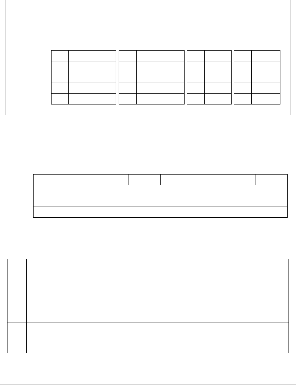
MOTOROLA Chapter 23. UART Modules 23-7
Register Descriptions
23.3.3 UART Status Registers (USRn)
The USRn registers, shown in Figure 23-4, show the status of the transmitter, the receiver,
and the FIFO.
Table 23-4 describes USRn fields.
3–0 SB Stop-bit length control. Selects the length of the stop bit appended to the transmitted character. Stop-bit lengths of
9/16th to 2 bits are programmable for 6–8 bit characters. Lengths of 1 1/16th to 2 bits are programmable for 5-bit
characters. In all cases, the receiver checks only for a high condition at the center of the first stop-bit position, that
is, one bit time after the last data bit or after the parity bit, if parity is enabled. If an external 1x clock is used for the
transmitter, clearing bit 3 selects one stop bit and setting bit 3 selects two stop bits for transmission.
SB 5 Bits 6–8 Bits SB 5 Bits 6–8 Bits SB 5–8 Bits SB 5–8 Bits
0000 1.063 0.563 0100 1.313 0.813 1000 1.563 1100 1.813
0001 1.125 0.625 0101 1.375 0.875 1001 1.625 1101 1.875
0010 1.188 0.688 0110 1.438 0.938 1010 1.688 1110 1.938
0011 1.250 0.750 0111 1.500 1.000 1011 1.750 1111 2.000
76543210
Field RB FE PE OE TxEMP TxRDY FFULL RxRDY
Reset 0000_0000
R/W Read only
Address IPSBAR + 0x204 (USR0), 0x244 (USR1), 0x284 (USR2)
Figure 23-4. UART Status Register (USRn)
Table 23-4. USRn Field Descriptions
Bits Name Description
7 RB Received break. The received break circuit detects breaks that originate in the middle of a received character.
However, a break in the middle of a character must persist until the end of the next detected character time.
0 No break was received.
1 An all-zero character of the programmed length was received without a stop bit. RB is valid only when
RxRDY = 1. Only a single FIFO position is occupied when a break is received. Further entries to the FIFO
are inhibited until RXD returns to the high state for at least one-half bit time, which is equal to two
successive edges of the UART clock. RB is valid only when RxRDY = 1.
6 FE Framing error.
0 No framing error occurred.
1 No stop bit was detected when the corresponding data character in the FIFO was received. The stop-bit
check occurs in the middle of the first stop-bit position. FE is valid only when RxRDY = 1.
Table 23-3. UMR2n Field Descriptions (continued)
Bits Name Description

23-8 MCF5282 User’s Manual MOTOROLA
Register Descriptions
23.3.4 UART Clock Select Registers (UCSRn)
The UCSRs select an external clock on the DTIN input (divided by 1 or 16) or a prescaled
system clock as the clocking source for the transmitter and receiver. See Section 23.5.1,
“Transmitter/Receiver Clock Source.” The transmitter and receiver can use different clock
sources. To use the system clock for both, set UCSRn to 0xDD.
Table 23-5 describes UCSRn fields.
5 PE Parity error. Valid only if RxRDY = 1.
0 No parity error occurred.
1 If UMR1n[PM] = 0x (with parity or force parity), the corresponding character in the FIFO was received with
incorrect parity. If UMR1n[PM] = 11 (multidrop), PE stores the received address or data (A/D) bit. PE is
valid only when RxRDY = 1.
4 OE Overrun error. Indicates whether an overrun occurs.
0 No overrun occurred.
1 One or more characters in the received data stream have been lost. OE is set upon receipt of a new character
when the FIFO is full and a character is already in the shift register waiting for an empty FIFO position.
When this occurs, the character in the receiver shift register and its break detect, framing error status, and
parity error, if any, are lost. OE is cleared by the RESET ERROR STATUS command in UCRn.
3 TxEMP Transmitter empty.
0 The transmit buffer is not empty. Either a character is being shifted out, or the transmitter is disabled. The
transmitter is enabled/disabled by programming UCRn[TC].
1 The transmitter has underrun (both the transmitter holding register and transmitter shift registers are empty).
This bit is set after transmission of the last stop bit of a character if there are no characters in the transmitter
holding register awaiting transmission.
2 TxRDY Transmitter ready.
0 The CPU loaded the transmitter holding register or the transmitter is disabled.
1 The transmitter holding register is empty and ready for a character. TxRDY is set when a character is sent
to the transmitter shift register or when the transmitter is first enabled. If the transmitter is disabled,
characters loaded into the transmitter holding register are not sent.
1 FFULL FIFO full.
0 The FIFO is not full but may hold up to two unread characters.
1 A character was received and the receiver FIFO is now full. Any characters received when the FIFO is full
are lost.
0 RxRDY Receiver ready.
0 The CPU has read the receive buffer and no characters remain in the FIFO after this read.
1 One or more characters were received and are waiting in the receive buffer FIFO.
7430
Field RCS TCS
Reset 0000_0000
R/W Write only
Address IPSBAR + 0x204 (UCSR0), 0x244 (UCSR1), 0x284 (UCSR2)
Figure 23-5. UART Clock Select Register (UCSRn)
Table 23-4. USRn Field Descriptions (continued)
Bits Name Description

MOTOROLA Chapter 23. UART Modules 23-9
Register Descriptions
23.3.5 UART Command Registers (UCRn)
The UCRs, shown in Figure 23-6, supply commands to the UART. Only multiple
commands that do not conflict can be specified in a single write to a UCRn. For example,
RESET TRANSMITTER and ENABLE TRANSMITTER cannot be specified in one command.
Table 23-6 describes UCRn fields and commands. Examples in Section 23.5.2,
“Transmitter and Receiver Operating Modes,” show how these commands are used.
Table 23-5. UCSRn Field Descriptions
Bits Name Description
7–4 RCS Receiver clock select. Selects the clock source for the receiver channel.
1101 Prescaled system clock
1110 DTIN divided by 16
1111 DTIN
3–0 TCS Transmitter clock select. Selects the clock source for the transmitter channel.
1101 Prescaled system clock
1110 DTIN divided by 16
1111 DTIN
76 43210
Field — MISC TC RC
Reset 0000_0000
R/W Write only
Address IPSBAR + 0x208(UCR0), 0x248(UCR1), 0x288(UCR2)
Figure 23-6. UART Command Register (UCRn)

23-10 MCF5282 User’s Manual MOTOROLA
Register Descriptions
Table 23-6. UCRn Field Descriptions
Bits Value Command Description
6–4 MISC Field (This field selects a single command.)
000 NO COMMAND —
001 RESET MODE
REGISTER POINTER
Causes the mode register pointer to point to UMR1n.
010 RESET RECEIVER Immediately disables the receiver, clears USRn[FFULL,RxRDY], and reinitializes the
receiver FIFO pointer. No other registers are altered. Because it places the receiver in a
known state, use this command instead of RECEIVER DISABLE when reconfiguring the
receiver.
011 RESET TRANSMITTER Disables the transmitter and clears USRn[TxEMP,TxRDY]. No other registers are altered.
Because it places the transmitter in a known state, use this command instead of
TRANSMITTER DISABLE when reconfiguring the transmitter.
100 RESET ERROR STATUS Clears USRn[RB,FE,PE,OE]. Also used in block mode to clear all error bits after a data
block is received.
101 RESET BREAK–
CHANGE INTERRUPT
Clears the delta break bit, UISRn[DB].
110 START BREAK Forces UTXD low. If the transmitter is empty, the break may be delayed up to one bit time.
If the transmitter is active, the break starts when character transmission completes. The
break is delayed until any character in the transmitter shift register is sent. Any character
in the transmitter holding register is sent after the break. The transmitter must be enabled
for the command to be accepted. This command ignores the state of CTS.
111 STOP BREAK Causes UTXD to go high (mark) within two bit times. Any characters in the transmit buffer
are sent.
3–2 TC Field (This field selects a single command)
00 NO ACTION TAKEN Causes the transmitter to stay in its current mode: if the transmitter is enabled, it remains
enabled; if the transmitter is disabled, it remains disabled.
01 TRANSMITTER
ENABLE
Enables operation of the channel’s transmitter. USRn[TxEMP,TxRDY] are set. If the
transmitter is already enabled, this command has no effect.
10 TRANSMITTER
DISABLE
Terminates transmitter operation and clears USRn[TxEMP,TxRDY]. If a character is being
sent when the transmitter is disabled, transmission completes before the transmitter
becomes inactive. If the transmitter is already disabled, the command has no effect.
11 — Reserved, do not use.

MOTOROLA Chapter 23. UART Modules 23-11
Register Descriptions
23.3.6 UART Receive Buffers (URBn)
The receive buffers contain one serial shift register and three receiver holding registers,
which act as a FIFO. RXD is connected to the serial shift register. The CPU reads from the
top of the stack while the receiver shifts and updates from the bottom when the shift register
is full (see Figure 23-19). RB contains the character in the receiver.
23.3.7 UART Transmit Buffers (UTBn)
The transmit buffers consist of the transmitter holding register and the transmitter shift
register. The holding register accepts characters from the bus master if channel’s
USRn[TxRDY] is set. A write to the transmit buffer clears USRn[TxRDY], inhibiting any
more characters until the shift register can accept more data. When the shift register is
empty, it checks if the holding register has a valid character to be sent (TxRDY = 0). If there
is a valid character, the shift register loads it and sets USRn[TxRDY] again. Writes to the
transmit buffer when the channel’s TxRDY = 0 and when the transmitter is disabled have
no effect on the transmit buffer.
1–0 RC (This field selects a single command)
00 NO ACTION TAKEN Causes the receiver to stay in its current mode. If the receiver is enabled, it remains
enabled; if disabled, it remains disabled.
01 RECEIVER ENABLE If the UART module is not in multidrop mode (UMR1n[PM] ≠ 11), RECEIVER ENABLE
enables the channel's receiver and forces it into search-for-start-bit state. If the receiver is
already enabled, this command has no effect.
10 RECEIVER DISABLE Disables the receiver immediately. Any character being received is lost. The command
does not affect receiver status bits or other control registers. If the UART module is
programmed for local loop-back or multidrop mode, the receiver operates even though this
command is selected. If the receiver is already disabled, the command has no effect.
11 — Reserved, do not use.
7 0
Field RB
Reset 1111_1111
R/W Read only
Address IPSBAR + 0x20C(URB0), 0x24C(URB1), 0x28C(URB2)
Figure 23-7. UART Receive Buffer (URBn)
Table 23-6. UCRn Field Descriptions (continued)
Bits Value Command Description
23-12 MCF5282 User’s Manual MOTOROLA
Register Descriptions
Figure 23-8 shows UTBn. TB contains the character in the transmit buffer.
23.3.8 UART Input Port Change Registers (UIPCRn)
The UIPCRs, shown in Figure 23-9, hold the current state and the change-of-state for CTS.
Table 23-7 describes UIPCRn fields.
7 0
Field TB
Reset 0000_0000
R/W Write only
Address IPSBAR + 0x20C(UTB0), 0x24C(UTB1), 0x28C(UTB2)
Figure 23-8. UART Transmit Buffer (UTBn)
7 543 10
Field — COS — CTS
Reset 0000 111 CTS
R/W Read only
Address IPSBAR + 0x210 (UIPCR0), 0x250 (UIPCR1), 0x290 (UIPCR2)
Figure 23-9. UART Input Port Change Register (UIPCRn)
Table 23-7. UIPCRn Field Descriptions
Bits Name Description
7–5 — Reserved, should be cleared.
4 COS Change of state (high-to-low or low-to-high transition).
0 No change-of-state since the CPU last read UIPCRn. Reading UIPCRn clears UISRn[COS].
1 A change-of-state longer than 25–50 µs occurred on the CTS input. UACRn can be programmed to
generate an interrupt to the CPU when a change of state is detected.
3–1 — Reserved, should be cleared.
0 CTS Current state of clear-to-send. Starting two serial clock periods after reset, CTS reflects the state of CTS. If
CTS is detected asserted at that time, COS is set, which initiates an interrupt if UACRn[IEC] is enabled.
0 The current state of the CTS input is asserted.
1 The current state of the CTS input is negated.

MOTOROLA Chapter 23. UART Modules 23-13
Register Descriptions
23.3.9 UART Auxiliary Control Register (UACRn)
The UACRs, shown in Figure 23-7, control the input enable.
Table 23-8 describes UACRn fields.
23.3.10 UART Interrupt Status/Mask Registers (UISRn/UIMRn)
The UISRs, shown in Figure 23-11, provide status for all potential interrupt sources. UISRn
contents are masked by UIMRn. If corresponding UISRn and UIMRn bits are set, the
internal interrupt output is asserted. If a UIMRn bit is cleared, the state of the corresponding
UISRn bit has no effect on the output.
NOTE
True status is provided in the UISRn regardless of UIMRn
settings. UISRn is cleared when the UART module is reset.
710
Field — IEC
Reset 0000_0000
R/W W
Address IPSBAR + 0x210 (UACR0), 0x250 (UACR1), 0x290 (UACR2)
Figure 23-10. UART Auxiliary Control Register (UACRn)
Table 23-8. UACRn Field Descriptions
Bits Name Description
7–1 — Reserved, should be cleared.
0 IEC Input enable control.
0 Setting the corresponding UIPCRn bit has no effect on UISRn[COS].
1 UISRn[COS] is set and an interrupt is generated when the UIPCRn[COS] is set by an external transition
on the CTS input (if UIMRn[COS] = 1).
76 32 1 0
UIMR
Field
COS — DB FFULL/RxRDY TxRDY
UISR
Field
COS — DB FFULL/RxRDY TxRDY
Reset 0000_0000
R/W Read only for status, write only for mask
Address IPSBAR + 0x214 (UISR0), 0x254 (UISR1), 0x294 (UISR2)
Figure 23-11. UART Interrupt Status/Mask Registers (UISRn/UIMRn)

23-14 MCF5282 User’s Manual MOTOROLA
Register Descriptions
Table 23-9 describes UISRn and UIMRn fields.
23.3.11 UART Baud Rate Generator Registers (UBG1n/UBG2n)
The UBG1n registers hold the MSB, and the UBG2n registers hold the LSB of the preload
value. UBG1n and UBG2n concatenate to provide a divider to the system clock for
transmitter/receiver operation, as described in Section 23.5.1.2.1, “System Clock Baud
Rates.”
Table 23-9. UISRn/UIMRn Field Descriptions
Bits Name Description
7 COS Change-of-state.
0UIPCRn[COS] is not selected.
1 Change-of-state occurred on CTS and was programmed in UACRn[IEC] to cause an interrupt.
6–3 — Reserved, should be cleared.
2 DB Delta break.
0 No new break-change condition to report. Section 23.3.5, “UART Command Registers (UCRn),”
describes the RESET BREAK-CHANGE INTERRUPT command.
1 The receiver detected the beginning or end of a received break.
1FFULL/
RxRDY
RxRDY (receiver ready) if UMR1n[FFULL/RxRDY] = 0; FIFO full (FFULL) if
UMR1n[FFULL/RxRDY] = 1. Duplicate of USRn[FFULL/RxRDY]. If FFULL is enabled for UART0
or UART1, DMA channels 2 or 3 are respectively interrupted when the FIFO is full.
0 TxRDY Transmitter ready. This bit is the duplication of USRn[TxRDY].
0 The transmitter holding register was loaded by the CPU or the transmitter is disabled. Characters
loaded into the transmitter holding register when TxRDY = 0 are not sent.
1 The transmitter holding register is empty and ready to be loaded with a character.
7 0
Field Divider MSB
Reset 0000_0000
R/W W
Address IPSBAR + 0x218 (UBG10), 0x258 (UBG11), 0x298 (UBG12)
Figure 23-12. UART Baud Rate Generator Register (UBG1n)
7 0
Field Divider LSB
Reset 0000_0000
R/W W
Address IPSBAR + 0x21C (UBG20), 0x25C (UBG21) 0x29C (UBG22)
Figure 23-13. UART Baud Rate Generator Register (UBG2n)

MOTOROLA Chapter 23. UART Modules 23-15
Register Descriptions
NOTE
The minimum value that can be loaded on the concatenation of
UBG1n with UBG2n is 0x0002. Both UBG1n and UBG2n are
write-only and cannot be read by the CPU.
23.3.12 UART Input Port Register (UIPn)
The UIPn registers, shown in Figure 23-14, show the current state of the CTS input.
Table 23-10 describes UIPn fields.
23.3.13 UART Output Port Command Registers (UOP1n/UOP0n)
The RTS output can be asserted by writing a 1 to UOP1n[RTS] and negated by writing a 1
to UOP0n[RTS]. See Figure 23-15.
Table 23-11 describes UOP1 and UOP0 fields.
710
Field — CTS
Reset 1111_1111
R/W R
Address IPSBAR + 0x234 (UIP0), 0x274 (UIP1), 0x2B4 (UIP2)
Figure 23-14. UART Input Port Register (UIPn)
Table 23-10. UIPn Field Descriptions
Bits Name Description
7–1 — Reserved, should be cleared.
0 CTS Current state of clear-to-send. The CTS value is latched and reflects the state of the input pin when UIPn
is read. Note: This bit has the same function and value as UIPCRn[RTS].
0 The current state of the CTS input is logic 0.
1 The current state of the CTS input is logic 1.
710
Field — RTS
Reset 0000_0000
R/W W
Addr UART0: IPSBAR + 0x238 (UOP1), 0x23C (UOP0); UART1 0x278 (UOP1), 0x27C (UOP0); UART2 0x2B8 (UOP1) 0x2BC
(UOP0)
Figure 23-15. UART Output Port Command Registers (UOP1n/UOP0n)

23-16 MCF5282 User’s Manual MOTOROLA
Register Descriptions
Table 23-11. UOP1/UOP0 Field Descriptions
Bits Name Description
7–1 — Reserved, should be cleared.
0 RTS Output port output. Controls assertion (UOP1)/negation (UOP0) of RTS output.
0 Not affected.
1 Asserts RTS with a write to UOP1. Negates RTS with a write to UOP0.
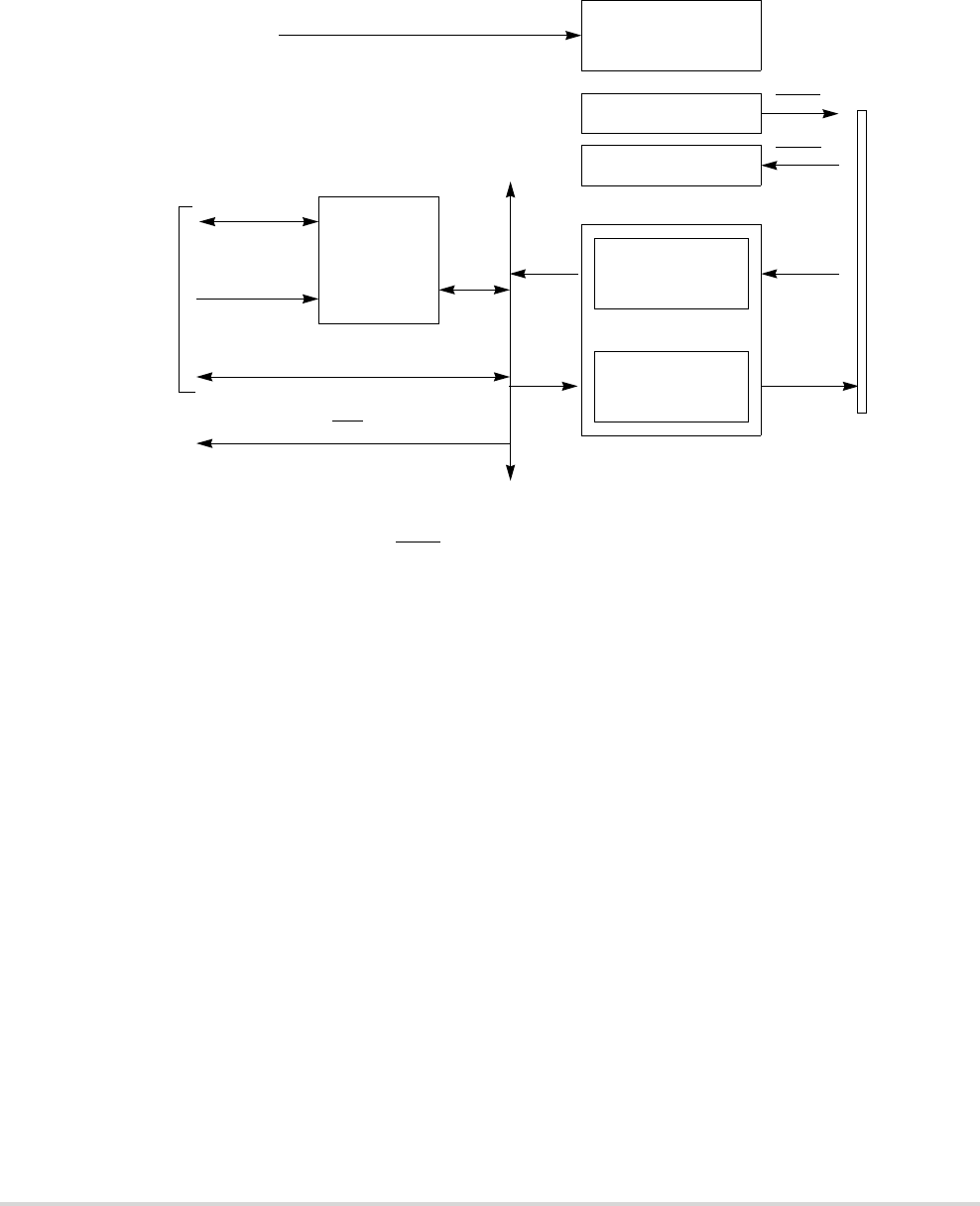
MOTOROLA Chapter 23. UART Modules 23-17
UART Module Signal Definitions
23.4 UART Module Signal Definitions
Figure 23-16 shows both the external and internal signal groups.
Figure 23-16. UART Block Diagram Showing External and Internal Interface Signals
An internal interrupt request signal (IRQ) is provided to notify the interrupt controller of an
interrupt condition. The output is the logical NOR of unmasked UISRn bits. The interrupt
level of a UART module is programmed in the interrupt controller.
The interrupt level and priority is programmed in the interrupt controller—ICR13 for
UART0, ICR14 for UART1, and ICR15 for UART2. See Section 10.3.6, “Interrupt Control
Register (ICRnx, (x = 1, 2,..., 63)).”
Note that the UARTs can also be configured to automatically transfer data by using the
DMA rather than interrupting the core. When the FIFO has data on the receive path, a DMA
request can be issued. For more information on generating DMA requests, refer to
Section 23.5.6.1.2, “Setting up the UART to Request DMA Service,” and Section 16.2,
“DMA Request Control (DMAREQC).”
Table 23-12 briefly describes the UART module signals.
NOTE
The terms ‘assertion’ and ‘negation’ are used to avoid
confusion between active-low and active-high signals.
‘Asserted’ indicates that a signal is active, independent of the
voltage level; ‘negated’ indicates that a signal is inactive.
Internal
Four-Character
Receive Buffer
Two-Character
Transmit Buffer
Input Port
Output Port
Interface
UART Module
Address Bus
Control
UCTS
URTS
URXD
UTXD
Control
Logic
or
Internal Bus
Data
to CPU
IRQ
To Interrupt
Controller
External
Interface
Signals
System Clock Clock Source
Generator
or DMA
External Clock (DTIN)
23-18 MCF5282 User’s Manual MOTOROLA
Operation
Figure 23-17 shows a signal configuration for a UART/RS-232 interface.
Figure 23-17. UART/RS-232 Interface
23.5 Operation
This section describes operation of the clock source generator, transmitter, and receiver.
23.5.1 Transmitter/Receiver Clock Source
The system clock serves as the basic timing reference for the clock source generator logic,
which consists of a clock generator and a programmable 16-bit divider dedicated to each
UART. The clock generator might not produce standard baud rates if the system clock is
used, so the 16-bit divider should be used.
23.5.1.1 Programmable Divider
As Figure 23-18 shows, the UARTn transmitter and receiver can use the following clock
sources:
• An external clock signal on the DTINn pin that can be divided by 16. When not
divided, DTINn provides a synchronous clock mode; when divided by 16, it is
asynchronous.
Table 23-12. UART Module Signals
Signal Description
Transmitter Serial
Data Output
(UTXDn)
UTXDn is held high (mark condition) when the transmitter is disabled, idle, or operating in the local
loop-back mode. Data is shifted out on UTXDn on the falling edge of the clock source, with the least
significant bit (lsb) sent first.
Receiver Serial
Data Input
(URXDn)
Data received on URXDn is sampled on the rising edge of the clock source, with the lsb received first.
Clear-to-
Send (UCTSn)
This input can generate an interrupt on a change of state.
Request-to-
Send (URTSn)
This output can be programmed to be negated or asserted automatically by either the receiver or the
transmitter. When connected to a transmitter’s UCTSn, URTSn can control serial data flow.
URTSn
DO2
DI1
UCTSn
UTXDn
URXDn
DI2
DO1
RS-232 TransceiverUART
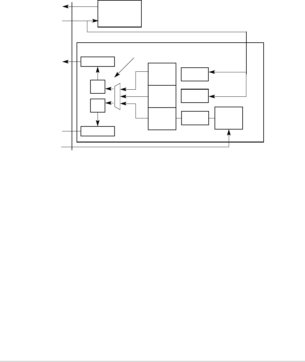
MOTOROLA Chapter 23. UART Modules 23-19
Operation
• The system clock supplies an asynchronous clock source that is divided by 32 and
then divided by the 16-bit value programmed in UBG1n and UBG2n. See
Section 23.3.11, “UART Baud Rate Generator Registers (UBG1n/UBG2n).”
The choice of DTIN or system clock is programmed in the UCSR.
Figure 23-18. Clocking Source Diagram
NOTE
If DTINn is a clocking source for either the timer or UART, that
timer module cannot use DTINn for timer capture.
23.5.1.2 Calculating Baud Rates
The following sections describe how to calculate baud rates.
23.5.1.2.1 System Clock Baud Rates
When the system clock is the UART clocking source, it goes through a divide-by-32
prescaler and then passes through the 16-bit divider of the concatenated UBG1n and
UBG2n registers. The baud-rate calculation is as follows:
Using a 66MHz system clock and letting baud rate = 9600, then
UART
On-Chip
DTIN
x1
Prescaler
x16
Prescaler
Clock
Generator
16-Bit
Divider
x32
Prescaler
DTIN
Clocking sources programmed in UCSR
Timer Module
DTOUTn
DTINn
UTXDn
URXDn
Tx
Rx
Rx Buffer
Tx Buffer
System
Clock
16-Bit
Divider
16-Bit
Divider
Baudrate SYSCLK
32 x divider[]
---------------------------------=
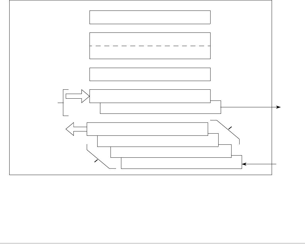
23-20 MCF5282 User’s Manual MOTOROLA
Operation
therefore UBG1n = 0x00 and UBG2n = 0xD6.
23.5.1.2.2 External Clock
An external source clock (DTINn) can be used as is or divided by 16.
23.5.2 Transmitter and Receiver Operating Modes
Figure 23-19 is a functional block diagram of the transmitter and receiver showing the
command and operating registers, which are described generally in the following sections
and described in detail in Section 23.3, “Register Descriptions.”
Figure 23-19. Transmitter and Receiver Functional Diagram
23.5.2.1 Transmitter
The transmitter is enabled through the UART command register (UCRn). When it is ready
to accept a character, the UART sets USRn[TxRDY]. The transmitter converts parallel data
Divider 66MHz
32 x 9600[]
---------------------------- 2 1 5 d e c i m a l()00D6 hexadecimal()== =
Baudrate Externalclockfrequency
16or1[]16bitdivider[]
----------------------------------------------------------------=
Receiver Shift Register
UART Command Register (UCRn)W
UART Status Register (USRn)R
Transmitter Shift Register
UART Mode Register 1 (UMR1n)R/W
UART Mode Register 2 (UMR2n)R/W
Transmitter Holding Register W
Receiver Holding Register 3
Receiver Holding Register 2
Receiver Holding Register 1 R
UART Receive
UART
Buffer (URBn)
(4 Registers)
UARTn
External
Interface
URXD
UTXD
Transmit Buffer
(UTBn)
(2 Registers)
FIFO

MOTOROLA Chapter 23. UART Modules 23-21
Operation
from the CPU to a serial bit stream on UTXDn. It automatically sends a start bit followed
by the programmed number of data bits, an optional parity bit, and the programmed number
of stop bits. The lsb is sent first. Data is shifted from the transmitter output on the falling
edge of the clock source.
After the stop bits are sent, if no new character is in the transmitter holding register, the
UTXDn output remains high (mark condition) and the transmitter empty bit,
USRn[TxEMP], is set. Transmission resumes and TxEMP is cleared when the CPU loads
a new character into the UART transmit buffer (UTBn). If the transmitter receives a disable
command, it continues until any character in the transmitter shift register is completely
sent.
If the transmitter is reset through a software command, operation stops immediately (see
Section 23.3.5, “UART Command Registers (UCRn)”). The transmitter is reenabled
through the UCRn to resume operation after a disable or software reset.
If the clear-to-send operation is enabled, UCTSn must be asserted for the character to be
transmitted. If UCTSn is negated in the middle of a transmission, the character in the shift
register is sent and UTXD remains in mark state until UCTSn is reasserted. If the
transmitter is forced to send a continuous low condition by issuing a SEND BREAK
command, the transmitter ignores the state of UCTSn.
If the transmitter is programmed to automatically negate URTSn when a message
transmission completes, URTSn must be asserted manually before a message is sent. In
applications in which the transmitter is disabled after transmission is complete and URTSn
is appropriately programmed, URTSn is negated one bit time after the character in the shift
register is completely transmitted. The transmitter must be manually reenabled by
reasserting URTSn before the next message is to be sent.
Figure 23-20 shows the functional timing information for the transmitter.
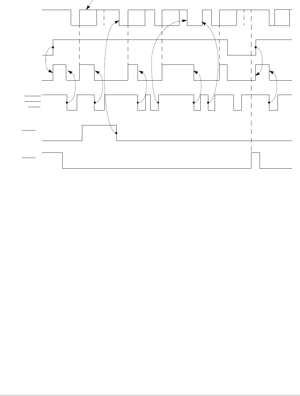
23-22 MCF5282 User’s Manual MOTOROLA
Operation
Figure 23-20. Transmitter Timing Diagram
23.5.2.2 Receiver
The receiver is enabled through its UCRn, as described in Section 23.3.5, “UART
Command Registers (UCRn).”
When the receiver detects a high-to-low (mark-to-space) transition of the start bit on
URXD, the state of URXD is sampled eight times on the edge of the bit time clock starting
one-half clock after the transition (asynchronous operation) or at the next rising edge of the
bit time clock (synchronous operation). If URXD is sampled high, the start bit is invalid
and the search for the valid start bit begins again.
If URXD is still low, a valid start bit is assumed and the receiver continues sampling the
input at one-bit time intervals, at the theoretical center of the bit, until the proper number
of data bits and parity, if any, is assembled and one stop bit is detected. Data on the URXD
input is sampled on the rising edge of the programmed clock source. The lsb is received
first. The data is then transferred to a receiver holding register and USRn[RxRDY] is set.
If the character is less than eight bits, the most significant unused bits in the receiver
holding register are cleared.
C1
1
C2 C3 Break C4 C6
UTXD
n
Transmitter
Enabled
U
SR
n
[TxRDY]
W
2
WWWWWWW
UCTS
n
3
URTS
n
4
Manually asserted
by
BIT
-
SET
command
Manually
asserted
Start
break
C5
not
transmitted
C6C4 Stop
break
C3C2C1
1
C1 in transmission
3
UMR2
n
[TxCTS] = 1
1
C
n
= transmit characters
2
W = write
4
UMR2
n
[TxRTS] = 1
internal
module
select
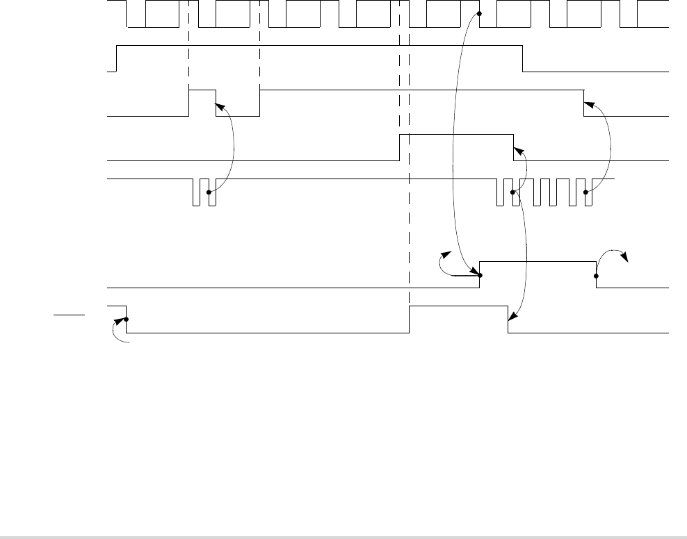
MOTOROLA Chapter 23. UART Modules 23-23
Operation
After the stop bit is detected, the receiver immediately looks for the next start bit. However,
if a non-zero character is received without a stop bit (framing error) and URXD remains
low for one-half of the bit period after the stop bit is sampled, the receiver operates as if a
new start bit were detected. Parity error, framing error, overrun error, and received break
conditions set the respective PE, FE, OE, RB error and break flags in the USRn at the
received character boundary and are valid only if USRn[RxRDY] is set.
If a break condition is detected (URXD is low for the entire character including the stop
bit), a character of all zeros is loaded into the receiver holding register and
USRn[RB,RxRDY] are set. URXD must return to a high condition for at least one-half bit
time before a search for the next start bit begins.
The receiver detects the beginning of a break in the middle of a character if the break
persists through the next character time. If the break begins in the middle of a character, the
receiver places the damaged character in the Rx FIFO stack and sets the corresponding
USRn error bits and USRn[RxRDY]. Then, if the break lasts until the next character time,
the receiver places an all-zero character into the Rx FIFO and sets USRn[RB,RxRDY].
Figure 23-21 shows receiver functional timing.
Figure 23-21. Receiver Timing
23.5.2.3 FIFO Stack
The FIFO stack is used in the UART’s receive buffer logic. The stack consists of three
receiver holding registers. The receive buffer consists of the FIFO and a receiver shift
register connected to the URXD (see Figure 23-19). Data is assembled in the receiver shift
C1 C2 C4 C6 C7 C8
C3 C5
C6, C7, and C8 will be lost
(C2)
Status
Data
(C3)
Status
Data
(C4)
Status
Data
C5 will
be lost
Reset by
command
UTXDn
Receiver
Enabled
USR
n
[RxRDY]
Overrun
URTSn4
internal
module
select
USR
n
[FFULL]
(C1)
Status
Data
USR
n
[OE]
Automatically asserted
when ready to receive
Manually asserted first time,
automatically negated if overrun occurs
UOP0[RTS] = 1

23-24 MCF5282 User’s Manual MOTOROLA
Operation
register and loaded into the top empty receiver holding register position of the FIFO. Thus,
data flowing from the receiver to the CPU is quadruple-buffered.
In addition to the data byte, three status bits, parity error (PE), framing error (FE), and
received break (RB), are appended to each data character in the FIFO; OE (overrun error)
is not appended. By programming the ERR bit in the channel’s mode register (UMR1n),
status is provided in character or block modes.
USRn[RxRDY] is set when at least one character is available to be read by the CPU. A read
of the receive buffer produces an output of data from the top of the FIFO stack. After the
read cycle, the data at the top of the FIFO stack and its associated status bits are popped and
the receiver shift register can add new data at the bottom of the stack. The FIFO-full status
bit (FFULL) is set if all three stack positions are filled with data. Either the RxRDY or
FFULL bit can be selected to cause an interrupt or DMA request.
The two error modes are selected by UMR1n[ERR] as follows:
• In character mode (UMR1n[ERR] = 0, status is given in the USRn for the character
at the top of the FIFO.
• In block mode, the USRn shows a logical OR of all characters reaching the top of
the FIFO stack since the last RESET ERROR STATUS command. Status is updated as
characters reach the top of the FIFO stack. Block mode offers a data-reception speed
advantage where the software overhead of error-checking each character cannot be
tolerated. However, errors are not detected until the check is performed at the end of
an entire message—the faulting character is not identified.
In either mode, reading the USRn does not affect the FIFO. The FIFO is popped only when
the receive buffer is read. The USRn should be read before reading the receive buffer. If all
three receiver holding registers are full, a new character is held in the receiver shift register
until space is available. However, if a second new character is received, the contents of the
the character in the receiver shift register is lost, the FIFOs are unaffected, and USRn[OE]
is set when the receiver detects the start bit of the new overrunning character.
To support flow control, the receiver can be programmed to automatically negate and assert
URTSn, in which case the receiver automatically negates URTSn when a valid start bit is
detected and the FIFO stack is full. The receiver asserts URTSn when a FIFO position
becomes available; therefore, overrun errors can be prevented by connecting URTSn to the
UCTSn input of the transmitting device.
NOTE
The receiver can still read characters in the FIFO stack if the
receiver is disabled. If the receiver is reset, the FIFO stack,
URTSn control, all receiver status bits, and interrupts, and
DMA requests are reset. No more characters are received until
the receiver is reenabled.
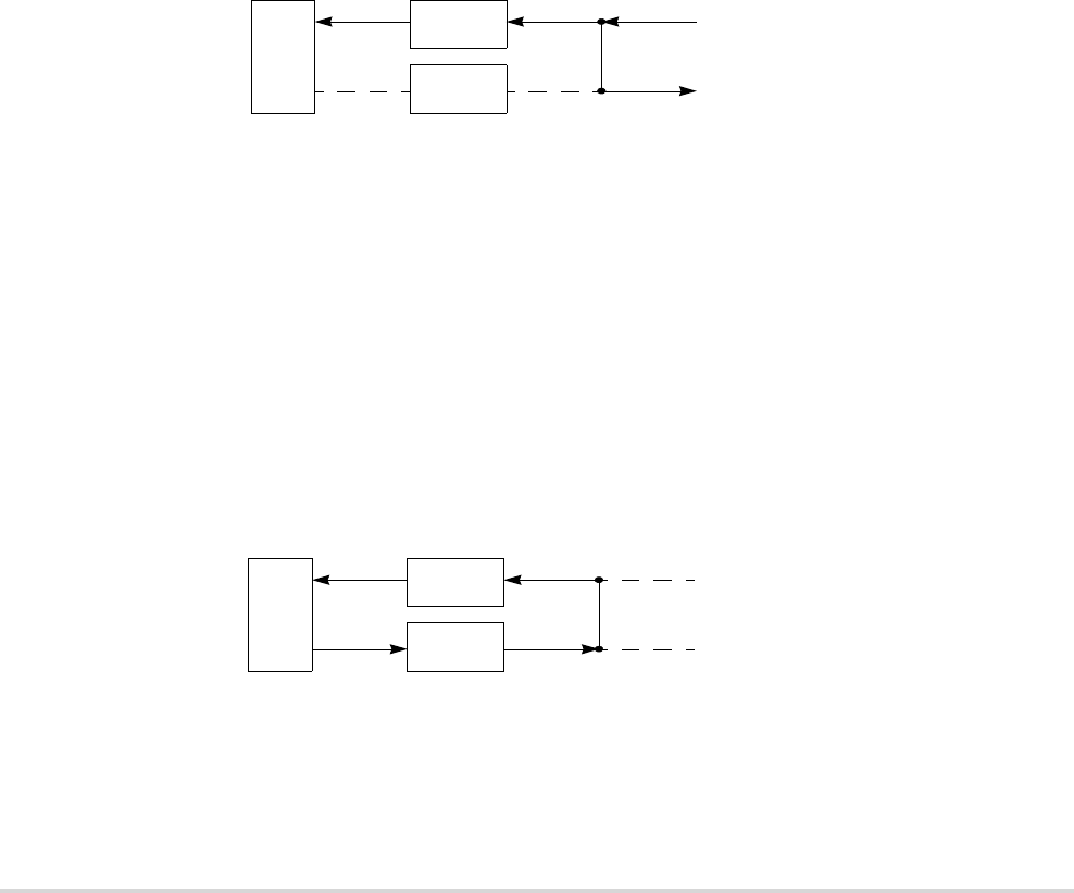
MOTOROLA Chapter 23. UART Modules 23-25
Operation
23.5.3 Looping Modes
The UART can be configured to operate in various looping modes as shown in
Figure 23-21. These modes are useful for local and remote system diagnostic functions.
The modes are described in the following paragraphs and in Section 23.3, “Register
Descriptions.”
The UART’s transmitter and receiver should be disabled when switching between modes.
The selected mode is activated immediately upon mode selection, regardless of whether a
character is being received or transmitted.
23.5.3.1 Automatic Echo Mode
In automatic echo mode, shown in Figure 23-22, the UART automatically resends received
data bit by bit. The local CPU-to-receiver communication continues normally, but the
CPU-to-transmitter link is disabled. In this mode, received data is clocked on the receiver
clock and re-sent on UTXD. The receiver must be enabled, but the transmitter need not be.
Figure 23-22. Automatic Echo
Because the transmitter is inactive, USRn[TxEMP,TxRDY] are inactive and data is sent as
it is received. Received parity is checked but is not recalculated for transmission. Character
framing is also checked, but stop bits are sent as they are received. A received break is
echoed as received until the next valid start bit is detected.
23.5.3.2 Local Loop-Back Mode
Figure 23-23 shows how UTXDn and URXDn are internally connected in local loop-back
mode. This mode is for testing the operation of a local UART module channel by sending
data to the transmitter and checking data assembled by the receiver to ensure proper
operations.
Figure 23-23. Local Loop-Back
Features of this local loop-back mode are as follows:
• Transmitter and CPU-to-receiver communications continue normally in this mode.
•URXDn input data is ignored
CPU
Disabled Disabled
URXDn Input
UTXDn Output
Tx
Rx
CPU
Disabled
Disabled URXDn Input
UTXDn Output
Tx
Rx
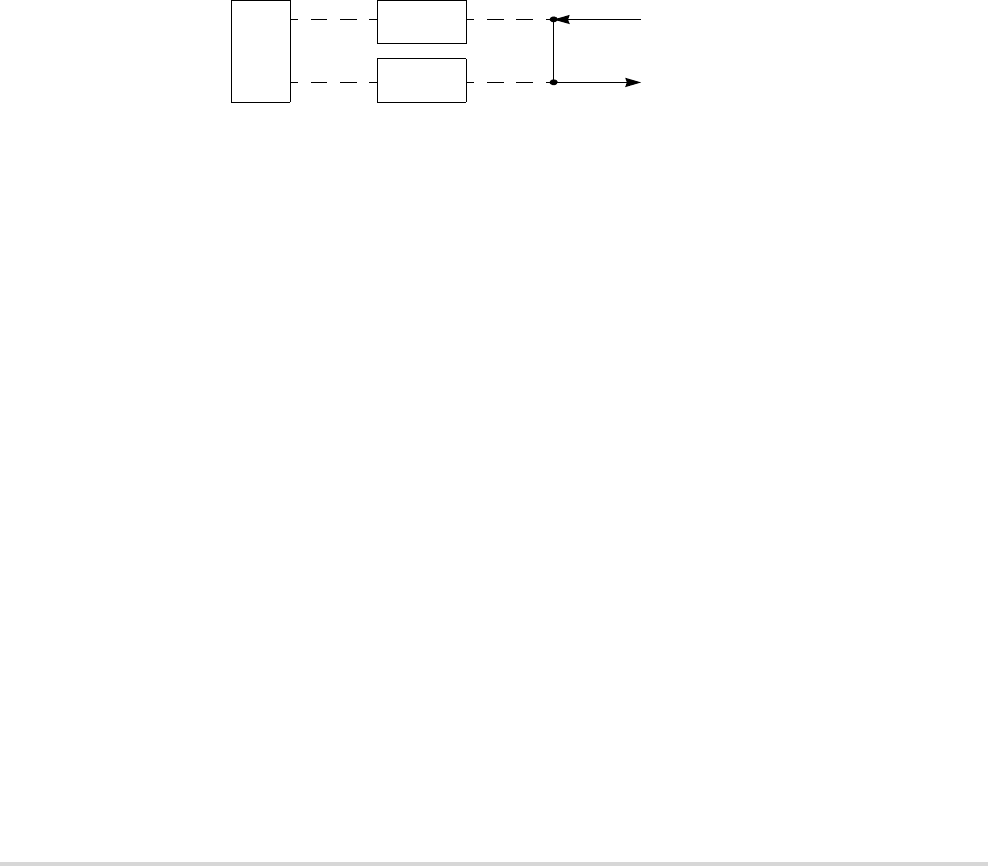
23-26 MCF5282 User’s Manual MOTOROLA
Operation
•UTXDn is held marking
• The receiver is clocked by the transmitter clock. The transmitter must be enabled,
but the receiver need not be.
23.5.3.3 Remote Loop-Back Mode
In remote loop-back mode, shown in Figure 23-24, the channel automatically transmits
received data bit by bit on the UTXDn output. The local CPU-to-transmitter link is
disabled. This mode is useful in testing receiver and transmitter operation of a remote
channel. For this mode, the transmitter uses the receiver clock.
Because the receiver is not active, received data cannot be read by the CPU and all status
conditions are inactive. Received parity is not checked and is not recalculated for
transmission. Stop bits are sent as they are received. A received break is echoed as received
until the next valid start bit is detected.
Figure 23-24. Remote Loop-Back
23.5.4 Multidrop Mode
Setting UMR1n[PM] programs the UART to operate in a wake-up mode for multidrop or
multiprocessor applications. In this mode, a master can transmit an address character
followed by a block of data characters targeted for one of up to 256 slave stations.
Although slave stations have their channel receivers disabled, they continuously monitor
the master’s data stream. When the master sends an address character, the slave receiver
channel notifies its respective CPU by setting USRn[RxRDY] and generating an interrupt
(if programmed to do so). Each slave station CPU then compares the received address to its
station address and enables its receiver if it wishes to receive the subsequent data characters
or block of data from the master station. Slave stations not addressed continue monitoring
the data stream. Data fields in the data stream are separated by an address character. After
a slave receives a block of data, its CPU disables the receiver and repeats the process.
Functional timing information for multidrop mode is shown in Figure 23-25.
CPU
Disabled
Disabled URXDn Input
UTXDn Input
Tx
Rx
Disabled
Disabled
MOTOROLA Chapter 23. UART Modules 23-27
Operation
Figure 23-25. Multidrop Mode Timing Diagram
A character sent from the master station consists of a start bit, a programmed number of
data bits, an address/data (A/D) bit flag, and a programmed number of stop bits. A/D = 1
indicates an address character; A/D = 0 indicates a data character. The polarity of A/D is
selected through UMR1n[PT]. UMR1n should be programmed before enabling the
transmitter and loading the corresponding data bits into the transmit buffer.
In multidrop mode, the receiver continuously monitors the received data stream, regardless
of whether it is enabled or disabled. If the receiver is disabled, it sets the RxRDY bit and
loads the character into the receiver holding register FIFO stack provided the received A/D
bit is a one (address tag). The character is discarded if the received A/D bit is zero (data
tag). If the receiver is enabled, all received characters are transferred to the CPU through
the receiver holding register stack during read operations.
In either case, the data bits are loaded into the data portion of the stack while the A/D bit is
loaded into the status portion of the stack normally used for a parity error (USRn[PE]).
Framing error, overrun error, and break detection operate normally. The A/D bit takes the
place of the parity bit; therefore, parity is neither calculated nor checked. Messages in this
mode may still contain error detection and correction information. One way to provide error
ADD1UTXDn
Transmitter
Enabled
USR
n
[TxRDY]
C0 ADD211
internal
module
select
A/D A/D A/D
ADD1URXDn
Receiver
Enabled
USR
n
[RxRDY]
C0 ADD211
internal
module
select
A/D A/D A/D
0
A/D
0
A/D
(C0)
Status Data
(ADD 2)
Status DataADD 1
Peripheral Station
Master Station
UMR1n[PM] = 11
UMR1n[PM] = 11
UMR1n[PT] = 1
ADD 1
UMR1n[PT] = 0
C0
UMR1n[PT] = 2
ADD 2
UMR1n[PM] = 11

23-28 MCF5282 User’s Manual MOTOROLA
Operation
detection, if 8-bit characters are not required, is to use software to calculate parity and
append it to the 5-, 6-, or 7-bit character.
23.5.5 Bus Operation
This section describes bus operation during read, write, and interrupt acknowledge cycles
to the UART module.
23.5.5.1 Read Cycles
The UART module responds to reads with byte data. Reserved registers return zeros.
23.5.5.2 Write Cycles
The UART module accepts write data as bytes. Write cycles to read-only or reserved
registers complete normally without exception processing, but data is ignored.
23.5.6 Programming
The software flowchart, Figure 23-26, consists of the following:
• UART module initialization—These routines consist of SINIT and CHCHK (sheets
1 and 2). Before SINIT is called at system initialization, the calling routine allocates
2 words on the system stack. On return to the calling routine, SINIT passes UART
status data on the stack. If SINIT finds no errors, the transmitter and receiver are
enabled. SINIT calls CHCHK to perform the checks. When called, SINIT places the
UART in local loop-back mode and checks for the following errors:
— Transmitter never ready
— Receiver never ready
— Parity error
— Incorrect character received
• I/O driver routine—This routine (sheets 4 and 5) consists of INCH, the terminal
input character routine which gets a character from the receiver, and OUTCH, which
sends a character to the transmitter.
• Interrupt handling—Consists of SIRQ (sheet 4), which is executed after the UART
module generates an interrupt caused by a change-in-break (beginning of a break).
SIRQ then clears the interrupt source, waits for the next change-in-break interrupt
(end of break), clears the interrupt source again, then returns from exception
processing to the system monitor.

MOTOROLA Chapter 23. UART Modules 23-29
Operation
23.5.6.1 Interrupt and DMA Request Initialization
23.5.6.1.1 Setting up the UART to Generate Core Interrupts
The list below gives the steps needed to properly initialize the UART to generate an
interrupt request to the core.
1. Initialize ICRx register in the interrupt controller (ICR13 for UART0, ICR14 for
UART1, and ICR15 for UART2)
2. Unmask appropriate bits in IMR in the interrupt controller (bits 13-15 for
UART0-UART2 respectively)
3. Verify DMAREQC (in SCM) does not assign UARTs to DMA channels
4. Initialize interrupts in the UART, see Table 23-13
23.5.6.1.2 Setting up the UART to Request DMA Service
The UART DMA request pin uses its interrupt pin to connect to the DMA. The user must
mask the UART interrupt in the interrupt control register when DMA requests are required.
The DMA should be configured for external requests (using the DMAREQC register) and
the source address set to the UART’s receive buffer (URB).
The UART may request DMA transfers on FIFO not empty or FIFO full. The user selects
the request source by setting bit 6 in the UART’s mode register 1 (UMR1). Setting UMR1
bit 6 = 0 allows DMA request on FIFO not empty, while setting UMR1 bit 6 = 1 allows
DMA requests on FIFO full. The user should then set bit 1 in the UART interrupt mask
register (UIMR[FFULL]).
In the case where DMA requests are set for UART FIFO full condition, once all the FIFO
stack positions are filled with data, the UART asserts its DMA request signal (via its
interrupt pin). Once the first data byte is read from the FIFO, the DMA request signal is
negated, and the FIFO stack is popped. However, the DMA may read the full contents of
the FIFO stack (if the DMA byte count register is set to 3 and the DMA control register is
not set for cycle steal).
Table 23-13. UART Interrupts
Register Bit Interrupt
UMR1x 6 RxIRQ
UIMRx 7 Change of State (COS)
UIMRx 2 Delta Break
UIMRx 1 RxFIFO Full
UIMRx 0 TxRDY

23-30 MCF5282 User’s Manual MOTOROLA
Operation
Although the UART receive buffer is quadruple-buffered, the receiver shift register is still
shifting its characters when the DMA request is ready to read its contents; therefore, the
maximum number of data bytes read during a UART DMA request transfer is three.
When the DMA is configured for cycle steal, only one character will be transferred on a
DMA request. This mode should be used for DMA requests on FIFO not empty. DMA
requests are negated when a data byte is read from the UART receive buffer.
The UART can be configured to request service from the DMA controller on a FIFO FULL
of RxRDY condition. The steps needed to intialize DMA requests from the UART are listed
below.
1. Mask appropriate bits in IMR (bits 13-15 for UART0-UART2 respectively)
2. Initialize DMAREQC to map UART DMA Request to a DMA channel
3. Initialize DMA request in UART, see Table 23-14
23.5.6.2 UART Module Initialization Sequence
Table 23-15 shows the UART module initialization sequence.
Table 23-14. UART DMA Requests
Register Bit Interrupt
UMR1x 6 RxIRQ.
0 DMA request on RxRDY
1 DMA request on FIFO full
UIMRx 1 RxFIFO full will enable DMA requests
Table 23-15. UART Module Initialization Sequence
Register Setting
UCRnReset the receiver and transmitter.
Reset the mode pointer (MISC[2–0] = 0b001).
UIVRnProgram the vector number for a UART module interrupt.
UIMRnEnable the preferred interrupt sources.
UACRnInitialize the input enable control (IEC bit).
UCSRnSelect the receiver and transmitter clock. Use timer as source if required.
UMR1nIf preferred, program operation of receiver ready-to-send (RxRTS bit).
Select receiver-ready or FIFO-full notification (RxRDY/FFULL bit).
Select character or block error mode (ERR bit).
Select parity mode and type (PM and PT bits).
Select number of bits per character (B/Cx bits).
UMR2nSelect the mode of operation (CMx bits).
If preferred, program operation of transmitter ready-to-send (TxRTS).
If preferred, program operation of clear-to-send (TxCTS bit).
Select stop-bit length (SBx bits).
UCR
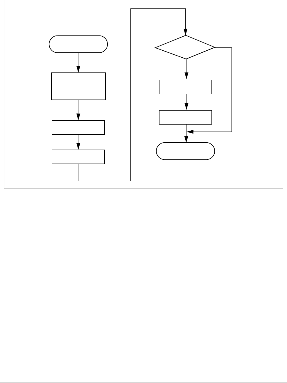
MOTOROLA Chapter 23. UART Modules 23-31
Operation
Figure 23-26. UART Mode Programming Flowchart (Sheet 1 of 5)
SERIAL MODULE
SINIT
INITIATE:
CHANNEL
INTERRUPTS
CHK1
CALL CHCHK
SAVE CHANNEL
STATUS
ENABLE
ANY
ERRORS
?
Y
N
ENABLE RECEIVER
ASSERT
REQUEST TO SEND
SINITR
RETURN
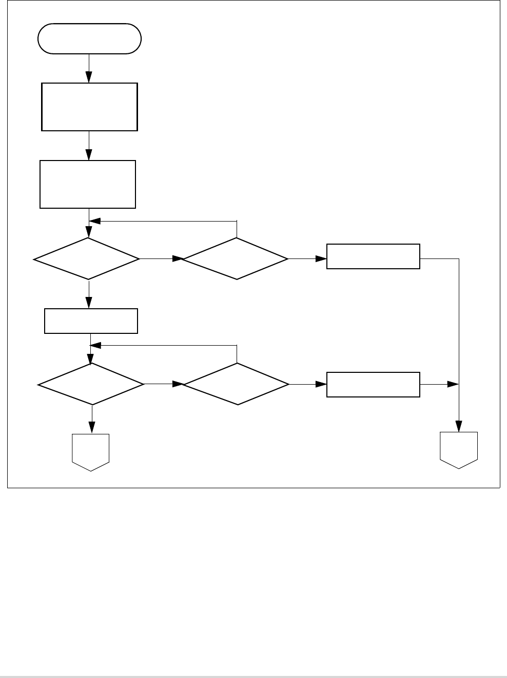
23-32 MCF5282 User’s Manual MOTOROLA
Operation
Figure 23-26. UART Mode Programming Flowchart (Sheet 2 of 5)
CHCHK
CHCHK
PLACE CHANNEL IN
LOCAL LOOPBACK
MODE
ENABLE
TRANSMITTER CLEAR
STATUS WORD
TxCHK
IS
TRANSMITTER
READY
?
Y
N
SNDCHR
RxCHK
SEND CHARACTER
TO TRANSMITTER
HAS
CHARACTER BEEN
RECEIVED
?
N
Y
A
WAI T E D
TOO LONG
?
N
N
WAI T ED
TOO LONG
?
Y
Y
SET TRANSMITTER-
NEVER-READY FLAG
SET RECEIVER-
NEVER-READY FLAG
B
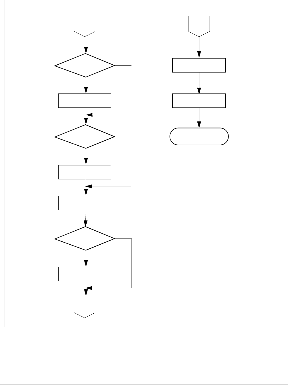
MOTOROLA Chapter 23. UART Modules 23-33
Operation
Figure 23-26. UART Mode Programming Flowchart (Sheet 3 of 5)
AB
B
FRCHK
HAVE
FRAMING ERROR
?
SET FRAMING
ERROR FLAG
PRCHK
HAVE
PARITY ERROR
?
SET PARITY
ERROR FLAG
GET CHARACTER
FROM RECEIVER
SAME AS
TRANSMITTED
CHARACTER
?
SET INCORRECT
CHARACTER FLAG
N
N
Y
CHRCHK
Y
N
DISABLE
TRANSMITTER
RSTCHN
RESTORE
TO ORIGINAL MODE
RETURN
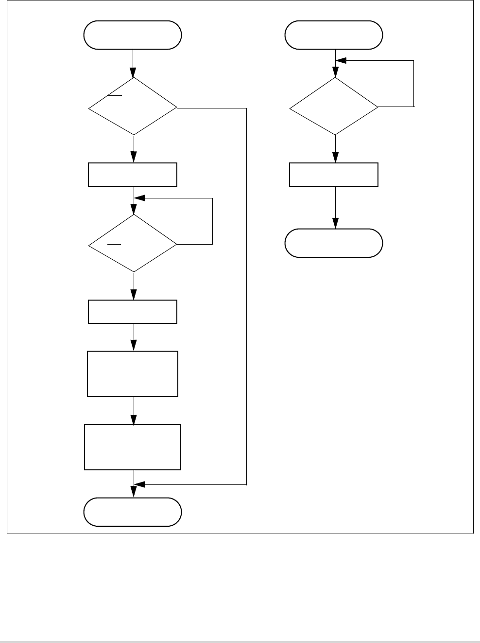
23-34 MCF5282 User’s Manual MOTOROLA
Operation
Figure 23-26. UART Mode Programming Flowchart (Sheet 4 of 5)
WAS
IRQ CAUSED
BY BEGINNING
OF A BREAK
?
SIRQ
ABRKI
N
CLEAR CHANGE-IN-
BREAK STATUS BIT
ABRKI1
N
HAS
END-OF-BREAK
IRQ ARRIVED
YET
?
Y
Y
CLEAR CHANGE-IN-
BREAK STATUS BIT
REMOVE BREAK
CHARACTER FROM
RECEIVER FIFO
REPLACE RETURN
ADDRESS ON SYSTEM
STACK AND MONITOR
WARM START ADDRESS
SIRQR
RTE
N
Y
DOES
CHANNEL A
RECEIVER HAVE A
CHARACTER
?
INCH
PLACE CHARACTER
IN D0
RETURN
MOTOROLA Chapter 23. UART Modules 23-35
Operation
Figure 23-26. UART Mode Programming Flowchart (Sheet 5 of 5)
OUTCH
IS
TRANSMITTER
READY
?
N
Y
SEND CHARACTER
TO TRANSMITTER
RETURN

23-36 MCF5282 User’s Manual MOTOROLA
Operation

MOTOROLA Chapter 24. I2C Interface 24-1
Chapter 24
I2C Interface
This chapter describes the MCF5282MCF523x I2C module, including I2C protocol, clock
synchronization, and I2C programming model registers. It also provides extensive
programming examples.
24.1 Overview
I2C is a two-wire, bidirectional serial bus that provides a simple, efficient method of data
exchange, minimizing the interconnection between devices. This bus is suitable for
applications that require occasional communication between many devices over a short
distance. The flexible I2C bus allows additional devices to be connected to the bus for
expansion and system development.
The I2C system is a true multiple-master bus; it uses arbitration and collision detection to
prevent data corruption in the event that multiple devices attempt to control the bus
simultaneously. This feature supports complex applications with multiprocessor control
and can be used for rapid testing and alignment of end products through external
connections to an assembly-line computer.
24.2 Interface Features
The I2C module has the following key features:
• Compatibility with I2C bus standard version 2.1
• Support for 3.3V tolerant devices
• Multiple-master operation
• Software-programmable for one of 50 different serial clock frequencies
• Software-selectable acknowledge bit
• Interrupt-driven, byte-by-byte data transfer
• Arbitration-lost interrupt with automatic mode switching from master to slave
• Calling address identification interrupt
• START and STOP signal generation/detection
• Repeated START signal generation
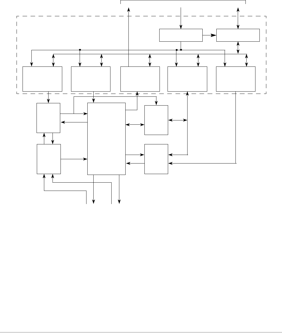
24-2 MCF5282 User’s Manual MOTOROLA
Interface Features
• Acknowledge bit generation/detection
• Bus-busy detection
Figure 24-1 is a block diagram of the I2C module.
Figure 24-1. I2C Module Block Diagram
Figure 24-1 shows the relationships of the I2C registers, listed below:
•I
2C address register (I2ADR)
•I
2C frequency divider register (I2FDR)
•I
2C control register (I2CR)
•I
2C status register (I2SR)
I2C data I/O register (I2DR)These registers are described in Section 24.5, “Programming
Model.”
Address
Compare
In/Out
Data
Shift
Start, Stop,
Input
Sync
Clock
Control
Registers and ColdFire Interface
Address Decode
I2C Address
Data MUX
SDASCL
AddressIRQ Data
and
Arbitration
Control
Register
Internal Bus
Register
(IADR)
I2C Frequency
Divider Register
(IFDR)
I2C Data
I/O Register
(I2DR)
I2C Status
Register
(I2SR)
I2C Control
Register
(I2CR)
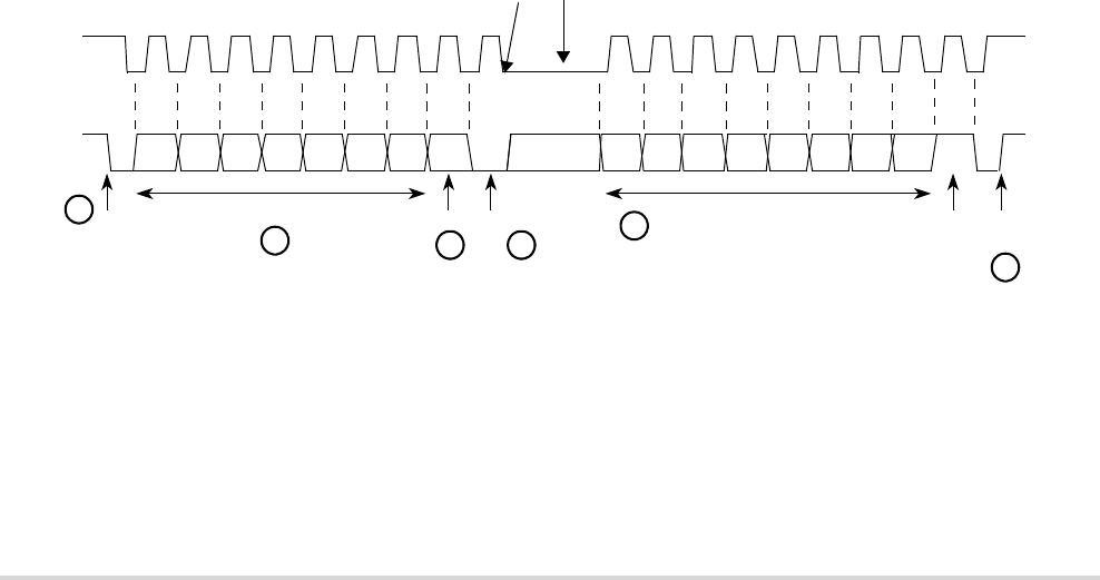
MOTOROLA Chapter 24. I2C Interface 24-3
I2C System Configuration
24.3 I2C System Configuration
The I2C module uses a serial data line (SDA) and a serial clock line (SCL) for data transfer.
For I2C compliance, all devices connected to these two signals must have open drain or
open collector outputs. The logic AND function is exercised on both lines with external
pull-up resistors.
Out of reset, the I2C default state is as a slave receiver. Thus, when not programmed to be
a master or responding to a slave transmit address, the I2C module should return to the
default slave receiver state. See Section 24.6.1, “Initialization Sequence,” for exceptions.
NOTE
The I2C module is designed to be compatible with the Philips
I2C bus protocol. For information on system configuration,
protocol, and restrictions, see The I2C Bus Specification,
Version 2.1.
24.4 I2C Protocol
Normally, a standard communication is composed of the following parts:
1. START signal—When no other device is bus master (both SCL and SDA lines are
at logic high), a device can initiate communication by sending a START signal (see
A in Figure 24-2). A START signal is defined as a high-to-low transition of SDA
while SCL is high. This signal denotes the beginning of a data transfer (each data
transfer can be several bytes long) and awakens all slaves.
Figure 24-2. I2C Standard Communication Protocol
2. Slave address transmission—The master sends the slave address in the first byte
after the START signal (B). After the seven-bit calling address, it sends the R/W bit
(C), which tells the slave data transfer direction.
Each slave must have a unique address. An I2C master must not transmit its own
slave address; it cannot be master and slave at the same time.
12345678 123456789 9
AD7 AD6 AD5 AD4 AD3 AD2 AD1 R/W XXX D7 D6 D5 D4 D3 D2 D1 D0
Calling Address R/W ACK
Bit
Data Byte No
ACK
Bit
STOP
Signal
lsbmsblsbmsb
SDA
SCL
START
Signal
A
BDC
E
F
SCL held low while
Interrupt is serviced
Interrupt bit set
(Byte complete)
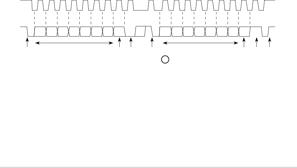
24-4 MCF5282 User’s Manual MOTOROLA
I2C Protocol
The slave whose address matches that sent by the master pulls SDA low at the ninth
serial clock (D) to return an acknowledge bit.
3. Data transfer—When successful slave addressing is achieved, the data transfer can
proceed (E) on a byte-by-byte basis in the direction specified by the R/W bit sent
by the calling master.
Data can be changed only while SCL is low and must be held stable while SCL is
high, as Figure 24-2 shows. SCL is pulsed once for each data bit, with the msb being
sent first. The receiving device must acknowledge each byte by pulling SDA low at
the ninth clock; therefore, a data byte transfer takes nine clock pulses.
If it does not acknowledge the master, the slave receiver must leave SDA high. The
master can then generate a STOP signal to abort the data transfer or generate a
START signal (repeated start, shown in Figure 24-3) to start a new calling sequence.
If the master receiver does not acknowledge the slave transmitter after a byte
transmission, it means end-of-data to the slave. The slave releases SDA for the
master to generate a STOP or START signal.
4. STOP signal—The master can terminate communication by generating a STOP
signal to free the bus. A STOP signal is defined as a low-to-high transition of SDA
while SCL is at logical high (F). Note that a master can generate a STOP even if the
slave has made an acknowledgment, at which point the slave must release the bus.
Instead of signaling a STOP, the master can repeat the START signal, followed by a calling
command, (A in Figure 24-3). A repeated START occurs when a START signal is
generated without first generating a STOP signal to end the communication.
Figure 24-3. Repeated START
The master uses a repeated START to communicate with another slave or with the same
slave in a different mode (transmit/receive mode) without releasing the bus.
24.4.1 Arbitration Procedure
If multiple devices simultaneously request the bus, the bus clock is determined by a
synchronization procedure in which the low period equals the longest clock-low period
among the devices and the high period equals the shortest. A data arbitration procedure
SCL 12345678 12 567834
AD7 AD6 AD5 AD4 AD3 AD2 AD1 R/W AD7 AD6 AD5 AD4 AD3 AD2 AD1 R/W
99
XX
New Calling Address R/W No
Stop
ACK
Bit
STOP
Signal
Repeated
START
Signal
ACK
Bit
R/W
Calling Address
START
SDA
msb lsb msb lsb
Signal
A
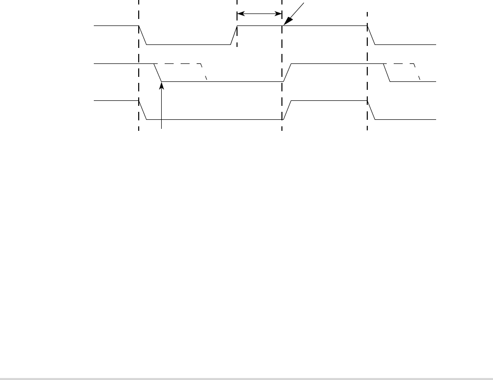
MOTOROLA Chapter 24. I2C Interface 24-5
I2C Protocol
determines the relative priority of competing devices. A device loses arbitration if it sends
logic high while another sends logic low; it immediately switches to slave-receive mode
and stops driving SDA. In this case, the transition from master to slave mode does not
generate a STOP condition. Meanwhile, hardware sets I2SR[IAL] to indicate loss of
arbitration.
24.4.2 Clock Synchronization
Since wire-AND logic is used, a high-to-low transition on SCL affects all devices
connected to the bus. Devices start counting their low period when the master drives SCL
low. When a device clock goes low, it holds SCL low until the clock high state is reached.
However, the low-to-high change in this device clock may not change the state of SCL if
another device clock is still in its low period. Therefore, the device with the longest low
period holds the synchronized clock SCL low. Devices with shorter low periods enter a high
wait state during this time (See Figure 24-4). When all devices involved have counted off
their low period, the synchronized clock SCL is released and pulled high. There is then no
difference between device clocks and the state of SCL, so all of the devices start counting
their high periods. The first device to complete its high period pulls SCL low again.
Figure 24-4. Synchronized Clock SCL
24.4.3 Handshaking
The clock synchronization mechanism can be used as a handshake in data transfers. Slave
devices can hold SCL low after completing one byte transfer (9 bits). In such a case, the
clock mechanism halts the bus clock and forces the master clock into wait states until the
slave releases SCL.
24.4.4 Clock Stretching
Slaves can use the clock synchronization mechanism to slow down the transfer bit rate.
After the master has driven SCL low, the slave can drive SCL low for the required period
and then release it. If the slave SCL low period is longer than the master SCL low period,
the resulting SCL bus signal low period is stretched.
Internal Counter Reset
SCL1
SCL2
SCL
Wait Start counting high period
24-6 MCF5282 User’s Manual MOTOROLA
Programming Model
24.5 Programming Model
Table 24-1 lists the configuration registers used in the I2C interface.
24.5.1 I2C Address Register (I2ADR)
The I2ADR holds the address the I2C responds to when addressed as a slave. Note that it is
not the address sent on the bus during the address transfer.
Table 24-2 describes I2ADR fields.
Table 24-1. I2C Interface Memory Map
IPSBAR
Offset [31:24] [23:16] [15:8] [7:0]
0x300 I2C Address Register (I2ADR) [p. 24-6] Reserved
0x304 I2C Frequency Divider Register (I2FDR) [p. 24-7] Reserved
0x308 I2C Control Register (I2CR) [p. 24-8] Reserved
0x30C I2C Status Register (I2SR) [p. 24-9] Reserved
0x310 I2C Data I/O Register (I2DR) [p. 24-10] Reserved
710
Field ADR —
Reset 0000_0000
R/W R/W
Address IPSBAR + 0x300
Figure 24-5. I2C Address Register (I2ADR)
Table 24-2. I2ADR Field Descriptions
Bits Name Description
7–1 ADR Slave address. Contains the specific slave address to be used by the I2C module. Slave mode is the default I2C
mode for an address match on the bus.
0 — Reserved, should be cleared.
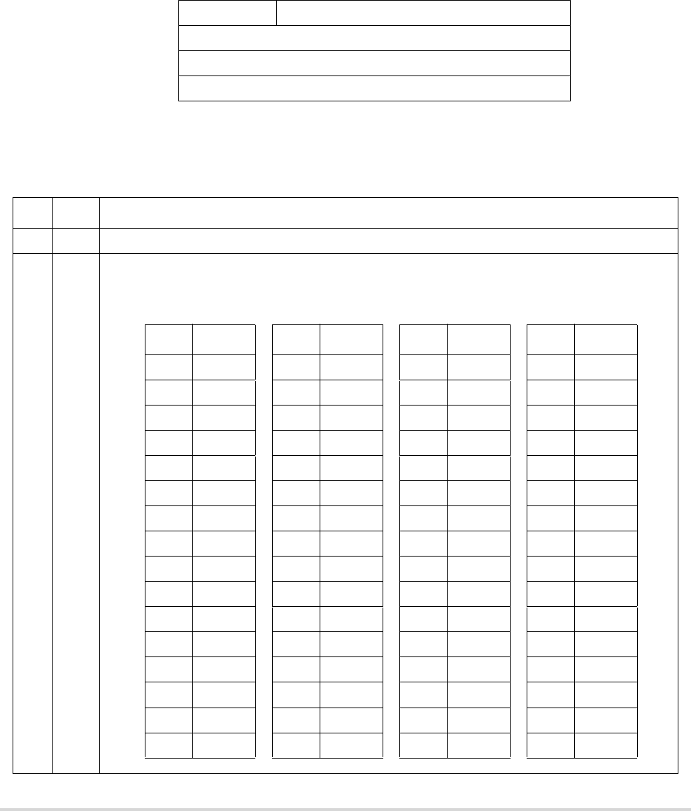
MOTOROLA Chapter 24. I2C Interface 24-7
Programming Model
24.5.2 I2C Frequency Divider Register (I2FDR)
The I2FDR, shown in Figure 24-6, provides a programmable prescaler to configure the I2C
clock for bit-rate selection.
Table 24-3 describes I2FDR[IC].
765 0
Field — IC
Reset 0000_0000
R/W R/W
Address IPSBAR + 0x304
Figure 24-6. I2C Frequency Divider Register (I2FDR)
Table 24-3. I2FDR Field Descriptions
Bits Name Description
7–6 — Reserved, should be cleared.
5–0 IC I2C clock rate. Prescales the clock for bit-rate selection. Due to potentially slow SCL and SDA rise and fall times,
bus signals are sampled at the prescaler frequency. The serial bit clock frequency is equal to the system clock
divided by the divider shown below.
IC Divider IC Divider IC Divider IC Divider
0x00 28 0x10 288 0x20 20 0x30 160
0x01 30 0x11 320 0x21 22 0x31 192
0x02 34 0x12 384 0x22 24 0x32 224
0x03 40 0x13 480 0x23 26 0x33 256
0x04 44 0x14 576 0x24 28 0x34 320
0x05 48 0x15 640 0x25 32 0x35 384
0x06 56 0x16 768 0x26 36 0x36 448
0x07 68 0x17 960 0x27 40 0x37 512
0x08 80 0x18 1152 0x28 48 0x38 640
0x09 88 0x19 1280 0x29 56 0x39 768
0x0A 104 0x1A 1536 0x2A 64 0x3A 896
0x0B 128 0x1B 1920 0x2B 72 0x3B 1024
0x0C 144 0x1C 2304 0x2C 80 0x3C 1280
0x0D 160 0x1D 2560 0x2D 96 0x3D 1536
0x0E 192 0x1E 3072 0x2E 112 0x3E 1792
0x0F 240 0x1F 3840 0x2F 128 0x3F 2048

24-8 MCF5282 User’s Manual MOTOROLA
Programming Model
24.5.3 I2C Control Register (I2CR)
The I2CR is used to enable the I2C module and the I2C interrupt. It also contains bits that
govern operation as a slave or a master.
Table 24-4 describes I2CR fields.
76543210
Field IEN IIEN MSTA MTX TXAK RSTA —
Reset 0000_0000
R/W R/W
Address IPSBAR + 0x308
Figure 24-7. I2C Control Register (I2CR)
Table 24-4. I2CR Field Descriptions
Bits Name Description
7IENI
2C enable. Controls the software reset of the entire I2C module. If the module is enabled in the middle of a byte
transfer, slave mode ignores the current bus transfer and starts operating when the next START condition is
detected. Master mode is not aware that the bus is busy; so initiating a start cycle may corrupt the current bus
cycle, ultimately causing either the current master or the I2C module to lose arbitration, after which bus
operation returns to normal.
0 The I2C module is disabled, but registers can still be accessed.
1 The I2C module is enabled. This bit must be set before any other I2CR bits have any effect.
6 IIEN I2C interrupt enable.
0 I2C module interrupts are disabled, but currently pending interrupt condition are not cleared.
1 I2C module interrupts are enabled. An I2C interrupt occurs if I2SR[IIF] is also set.
5 MSTA Master/slave mode select bit. If the master loses arbitration, MSTA is cleared without generating a STOP signal.
0 Slave mode. Changing MSTA from 1 to 0 generates a STOP and selects slave mode.
1 Master mode. Changing MSTA from 0 to 1 signals a START on the bus and selects master mode.
4 MTX Transmit/receive mode select bit. Selects the direction of master and slave transfers.
0 Receive
1 Transmit. When the MCF5282MCF523x is addressed as a slave, software should set MTX according to
I2SR[SRW]. In master mode, MTX should be set according to the type of transfer required. Therefore, when
the MCF5282MCF523x addresses a slave device, MTX is always 1.
3 TXAK Transmit acknowledge enable. Specifies the value driven onto SDA during acknowledge cycles for both master
and slave receivers. Note that writing TXAK applies only when the I2C bus is a receiver.
0 An acknowledge signal is sent to the bus at the ninth clock bit after receiving one byte of data.
1 No acknowledge signal response is sent (that is, acknowledge bit = 1).
2 RSTA Repeat start. Always read as 0. Attempting a repeat start without bus mastership causes loss of arbitration.
0 No repeat start
1 Generates a repeated START condition.
1–0 — Reserved, should be cleared.

MOTOROLA Chapter 24. I2C Interface 24-9
Programming Model
24.5.4 I2C Status Register (I2SR)
This I2SR contains bits that indicate transaction direction and status.
Table 24-5 describes I2SR fields.
76543210
Field ICF IAAS IBB IAL — SRW IIF RXAK
Reset 1000_0001
R/W R R/W RR/WR
Address IPSBAR + 0x30C
Figure 24-8. I2CR Status Register (I2SR)
Table 24-5. I2SR Field Descriptions
Bits Name Description
7 ICF Data transferring bit. While one byte of data is transferred, ICF is cleared.
0 Transfer in progress
1 Transfer complete. Set by the falling edge of the ninth clock of a byte transfer.
6IAAS I
2C addressed as a slave bit. The CPU is interrupted if I2CR[IIEN] is set. Next, the CPU must check SRW and
set its TX/RX mode accordingly. Writing to I2CR clears this bit.
0 Not addressed.
1 Addressed as a slave. Set when its own address (IADR) matches the calling address.
5 IBB I2C bus busy bit. Indicates the status of the bus.
0 Bus is idle. If a STOP signal is detected, IBB is cleared.
1 Bus is busy. When START is detected, IBB is set.
4 IAL Arbitration lost. Set by hardware in the following circumstances. (IAL must be cleared by software by writing
zero to it.)
• SDA sampled low when the master drives high during an address or data-transmit cycle.
• SDA sampled low when the master drives high during the acknowledge bit of a data-receive cycle.
• A start cycle is attempted when the bus is busy.
• A repeated start cycle is requested in slave mode.
• A stop condition is detected when the master did not request it.
3 — Reserved, should be cleared.
2 SRW Slave read/write. When IAAS is set, SRW indicates the value of the R/W command bit of the calling address
sent from the master. SRW is valid only when a complete transfer has occurred, no other transfers have been
initiated, and the I2C module is a slave and has an address match.
0 Slave receive, master writing to slave.
1 Slave transmit, master reading from slave.

24-10 MCF5282 User’s Manual MOTOROLA
I2C Programming Examples
24.5.5 I2C Data I/O Register (I2DR)
In master-receive mode, reading the I2DR, shown in Figure 24-9, allows a read to occur
and initiates next byte data receiving. In slave mode, the same function is available once
the I2C has received its slave address.
24.6 I2C Programming Examples
The following examples show programming for initialization, signaling START,
post-transfer software response, signalling STOP, and generating a repeated START.
24.6.1 Initialization Sequence
Before the interface can transfer serial data, registers must be initialized, as follows:
1. Set I2FDR[IC] to obtain SCL frequency from the system bus clock. See
Section 24.5.2, “I2C Frequency Divider Register (I2FDR).”
2. Update the I2ADR to define its slave address.
3. Set I2CR[IEN] to enable the I2C bus interface system.
4. Modify the I2CR to select or deselect master/slave mode, transmit/receive mode,
and interrupt-enable or not.
1IIFI
2C interrupt. Must be cleared by software by writing a zero to it in the interrupt routine.
0 No I2C interrupt pending
1 An interrupt is pending, which causes a processor interrupt request (if IIEN = 1). Set when one of the
following occurs:
• Complete one byte transfer (set at the falling edge of the ninth clock)
• Reception of a calling address that matches its own specific address in slave-receive mode
• Arbitration lost
0 RXAK Received acknowledge. The value of SDA during the acknowledge bit of a bus cycle.
0 An acknowledge signal was received after the completion of 8-bit data transmission on the bus
1 No acknowledge signal was detected at the ninth clock.
76543210
Field Data
Reset 0000_0000
R/W R/W
Address IPSBAR + 0x310
Figure 24-9. I2C Data I/O Register (I2DR)
Table 24-5. I2SR Field Descriptions (continued)
Bits Name Description

MOTOROLA Chapter 24. I2C Interface 24-11
I2C Programming Examples
NOTE
If I2SR[IBB] is set when the I2C bus module is enabled,
execute the following code sequence before proceeding with
normal initialization code. This issues a STOP command to the
slave device, placing it in idle state as if it were just
power-cycled on.
I2CR = 0x0
I2CR = 0xA0
dummy read of I2DR
I2SR = 0x0
I2CR = 0x0
24.6.2 Generation of START
After completion of the initialization procedure, serial data can be transmitted by selecting
the master transmitter mode. On a multiple-master bus system, I2SR[IBB] must be tested
to determine whether the serial bus is free. If the bus is free (IBB = 0), the START signal
and the first byte (the slave address) can be sent. The data written to the data register
comprises the address of the desired slave and the lsb indicates the transfer direction.
The free time between a STOP and the next START condition is built into the hardware that
generates the START cycle. Depending on the relative frequencies of the system clock and
the SCL period, it may be necessary to wait until the I2C is busy after writing the calling
address to the I2DR before proceeding with the following instructions.
The following example signals START and transmits the first byte of data (slave address):
CHFLAG MOVE.B I2SR,-(A0) ;Check I2SR[MBB]
BTST.B #5, (A0)+
BNE.S CHFLAG ;If I2SR[MBB] = 1, wait until it is clear
TXSTART MOVE.B I2CR,-(A0) ;Set transmit mode
BSET.B #4,(A0)
MOVE.B (A0)+, I2CR
MOVE.B I2CR, -(A0) ;Set master mode
BSET.B #5, (A0) ;Generate START condition
MOVE.B (A0)+, I2CR
MOVE.B CALLING,-(A0) ;Transmit the calling address, D0=R/W
MOVE.B (A0)+, I2DR
IFREE MOVE.B I2SR,-(A0) ;Check I2SR[MBB]
;If it is clear, wait until it is set.
BTST.B #5, (A0)+
BEQ.S IFREE;
24.6.3 Post-Transfer Software Response
Sending or receiving a byte sets the I2SR[ICF], which indicates one byte communication
is finished. I2SR[IIF] is also set. An interrupt is generated if the interrupt function is
enabled during initialization by setting I2CR[IIEN]. Software must first clear I2SR[IIF] in

24-12 MCF5282 User’s Manual MOTOROLA
I2C Programming Examples
the interrupt routine. I2SR[ICF] is cleared either by reading from I2DR in receive mode or
by writing to I2DR in transmit mode.
Software can service the I2C I/O in the main program by monitoring IIF if the interrupt
function is disabled. Polling should monitor IIF rather than ICF because that operation is
different when arbitration is lost.
When an interrupt occurs at the end of the address cycle, the master is always in transmit
mode; that is, the address is sent. If master receive mode is required I2CR[MTX] should be
toggled.
During slave-mode address cycles (I2SR[IAAS] = 1), I2SR[SRW] is read to determine the
direction of the next transfer. MTX is programmed accordingly. For slave-mode data cycles
(IAAS = 0), SRW is invalid. MTX should be read to determine the current transfer
direction.
The following is an example of a software response by a master transmitter in the interrupt
routine (see Figure 24-10).
I2SR LEA.L I2SR,-(A7) ;Load effective address
BCLR.B #1,(A7)+ ;Clear the IIF flag
MOVE.B I2CR,-(A7) ;Push the address on stack,
BTST.B #5,(A7)+ ;check the MSTA flag
BEQ.S SLAVE ;Branch if slave mode
MOVE.B I2CR,-(A7) ;Push the address on stack
BTST.B #4,(A7)+ ;check the mode flag
BEQ.S RECEIVE ;Branch if in receive mode
MOVE.B I2SR,-(A7) ;Push the address on stack,
BTST.B #0,(A7)+ ;check ACK from receiver
BNE.B END ;If no ACK, end of transmission
TRANSMIT MOVE.B DATABUF,-(A7) ;Stack data byte
MOVE.B (A7)+, I2DR ;Transmit next byte of data
24.6.4 Generation of STOP
A data transfer ends when the master signals a STOP, which can occur after all data is sent,
as in the following example.
MASTX MOVE.B I2SR, -(A7) ;If no ACK, branch to end
BTST.B #0,(A7)+
BNE.B END
MOVE.B TXCNT,D0 ;Get value from the transmitting counter
BEQ.S END ;If no more data, branch to end
MOVE.B DATABUF,-(A7) ;Transmit next byte of data
MOVE.B (A7)+,I2DR
MOVE.B TXCNT,D0 ;Decrease the TXCNT
SUBQ.L #1,D0
MOVE.B D0,TXCNT
BRA.S EMASTX;Exit
END LEA.L I2CR,-(A7) ;Generate a STOP condition
BCLR.B #5,(A7)+
EMASTX RTE ;Return from interrupt

MOTOROLA Chapter 24. I2C Interface 24-13
I2C Programming Examples
For a master receiver to terminate a data transfer, it must inform the slave transmitter by not
acknowledging the last data byte. This is done by setting I2CR[TXAK] before reading the
next-to-last byte. Before the last byte is read, a STOP signal must be generated, as in the
following example.
MASR MOVE.B RXCNT,D0 ;Decrease RXCNT
SUBQ.L #1,D0
MOVE.B D0,RXCNT
BEQ.S ENMASR ;Last byte to be read
MOVE.B RXCNT,D1 ;Check second-to-last byte to be read
EXTB.L D1
SUBI.L #1,D1;
BNE.S NXMAR ;Not last one or second last
LAMAR BSET.B #3,I2CR ;Disable ACK
BRA NXMAR
ENMASR BCLR.B #5,I2CR ;Last one, generate STOP signal
NXMAR MOVE.B I2DR,RXBUF ;Read data and store RTE
24.6.5 Generation of Repeated START
After the data transfer, if the master still wants the bus, it can signal another START
followed by another slave address without signalling a STOP, as in the following example.
RESTART MOVE.B I2CR,-(A7) ;Repeat START (RESTART)
BSET.B #2, (A7)
MOVE.B (A7)+, I2CR
MOVE.B CALLING,-(A7) ;Transmit the calling address, D0=R/W-
MOVE.B CALLING,-(A7)
MOVE.B (A7)+, I2DR
24.6.6 Slave Mode
In the slave interrupt service routine, software should poll the I2SR[IAAS] bit to determine
if the controller has received its slave address. If IAAS is set, software should set the
transmit/receive mode select bit (I2CR[MTX]) according to the I2SR[SRW]. Writing to the
I2CR clears the IAAS automatically. The only time IAAS is read as set is from the interrupt
at the end of the address cycle where an address match occurred; interrupts resulting from
subsequent data transfers will have IAAS cleared. A data transfer can now be initiated by
writing information to I2DR for slave transmits, or read from I2DR in slave-receive mode.
A dummy read of I2DR in slave/receive mode releases SCL, allowing the master to send
data.
In the slave transmitter routine, I2SR[RXAK] must be tested before sending the next byte
of data. Setting RXAK means an end-of-data signal from the master receiver, after which
software must switch it from transmitter to receiver mode. Reading I2DR then releases SCL
so that the master can generate a STOP signal.

24-14 MCF5282 User’s Manual MOTOROLA
I2C Programming Examples
24.6.7 Arbitration Lost
If several devices try to engage the bus at the same time, one becomes master. Hardware
immediately switches devices that lose arbitration to slave receive mode. Data output to
SDA stops, but SCL is still generated until the end of the byte during which arbitration is
lost. An interrupt occurs at the falling edge of the ninth clock of this transfer with
I2SR[IAL] = 1 and I2CR[MSTA] = 0.
If a device that is not a master tries to transmit or do a START, hardware inhibits the
transmission, clears MSTA without signalling a STOP, generates an interrupt to the CPU,
and sets IAL to indicate a failed attempt to engage the bus. When considering these cases,
the slave service routine should first test IAL and software should clear it if it is set.
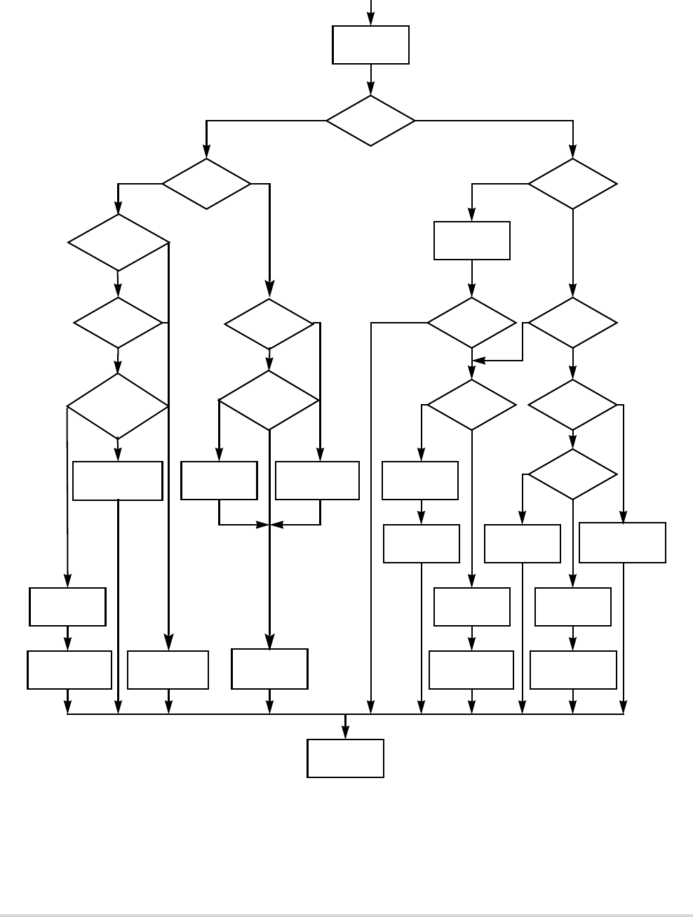
MOTOROLA Chapter 24. I2C Interface 24-15
I2C Programming Examples
Figure 24-10. Flow-Chart of Typical I2C Interrupt Routine
Clear
Master
Mode?
TX/Rx
?
Last Byte
Transmitted
?
RXAK= 0
?
End of
ADDR Cycle
(Master RX)
?
Write Next
Byte to I2DR
Switch to
Rx Mode
Dummy Read
from I2DR
Generate
STOP Signal
Read Data
from I2DR
And Store
Set TXAK =1 Generate
STOP Signal
2nd Last
Byte to be
Last
Byte to be
?
Arbitration
Lost?
Clear IAL
IAAS=1
?
IAAS=1
?
SRW=1
?Tx/Rx
?
Set TX
Mode
Write Data
to I2DR
Set RX
Mode
Dummy Read
from I2DR
ACK from
Receiver
?
Tx Next
Byte
Read Data
from I2DR
and Store
Switch to
Rx Mode
Dummy Read
from I2DR
RTE
YN
Y
Y
Y
Y
Y
Y
Y
Y
Y
N
N
N
N
N
N
N
N
N
Y
TX RX
RX
TX
(WRITE)
(Read)
N
IIF
Address
Cycle Data
Cycle
Read
Read?

24-16 MCF5282 User’s Manual MOTOROLA
I2C Programming Examples

MOTOROLA Chapter 25. FlexCAN 25-1
Chapter 25
FlexCAN
The FlexCAN module is a communication controller implementing the controller area
network (CAN) protocol, an asynchronous communications protocol used in automotive
and industrial control systems. It is a high speed (1 Mbit/sec), short distance, priority based
protocol which can communicate using a variety of mediums (for example, fiber optic cable
or an unshielded twisted pair of wires). The FlexCAN supports both the standard and
extended identifier (ID) message formats specified in the CAN protocol specification,
revision 2.0, part B.
The CAN protocol was primarily, but not only, designed to be used as a vehicle serial data
bus, meeting the specific requirements of this field: real-time processing, reliable operation
in the EMI environment of a vehicle, cost-effectiveness and required bandwidth. A general
working knowledge of the CAN protocol revision 2.0 is assumed in this document. For
details, refer to the CAN protocol revision 2.0 specification.
25.1 Features
• Based on and includes all existing Motorola TouCAN module features
• Motorola IP interface architecture
• Full implementation of the CAN protocol specification version 2.0
— Standard data and remote frames (up to 109 bits long)
— Extended data and remote frames (up to 127 bits long)
— 0–8 bytes data length
— Programmable bit rate up to 1Mbit/sec
• Up to 16 flexible message buffers of 0–8 bytes data length, each configurable as Rx
or Tx, all supporting standard and extended messages
• Listen-only mode capability
• Content-related addressing
• No read/write semaphores
• Three programmable mask registers: global (for MBs 0-13), special for MB14, and
special for MB15
• Programmable transmit-first scheme: lowest ID or lowest buffer number
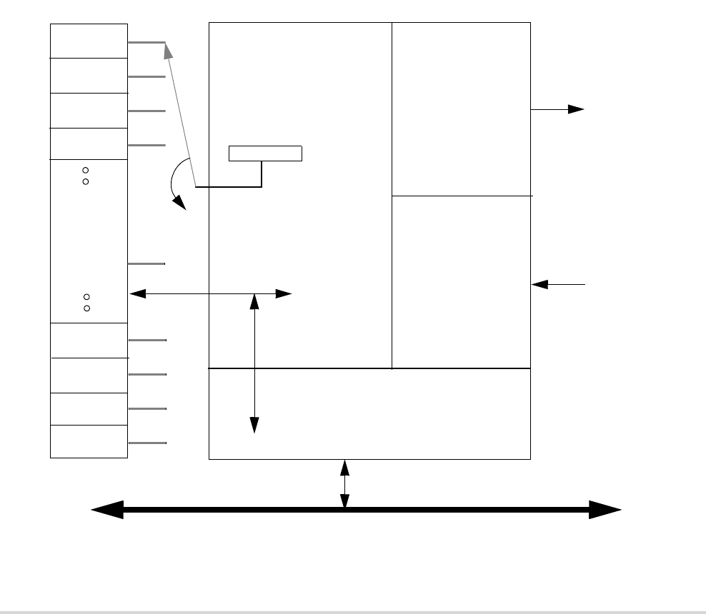
25-2 MCF5282 User’s Manual MOTOROLA
Features
• “Time Stamp”, based on 16-bit free-running timer
• Global network time, synchronized by a specific message
• Programmable I/O modes
• Maskable interrupts
• Independent of the transmission medium (external transceiver is assumed)
• Open network architecture
• Multimaster bus
• High immunity to EMI
• Short latency time for high-priority messages
• Low-power “sleep” mode, with programmable “wake up” on bus activity
A block diagram describing the various submodules of the FlexCAN module is shown in
Figure 25-1. Each submodule is described in detail in subsequent sections.
Figure 25-1. FlexCAN Block Diagram and Pinout
MB0
MB2
MB1
MB3
MB12
MB14
MB13
MB15
0.25k/0.5KB
RAM
Bus Interface Unit
MB #
(0-15)
Transmitter
Receiver
Control
CANTX
CANRX
Internal Bus

MOTOROLA Chapter 25. FlexCAN 25-3
Features
25.1.1 FlexCAN Memory Map
The FlexCAN module address space is split into 128 bytes starting at the base address, and
then an extra 256 bytes starting at the base address +128. The upper 256 are fully used for
the message buffer structures, as described in Section 25.3.2, “Message Buffer Memory
Map.” Out of the lower 128 bytes, only part is occupied by various registers.
Table 25-1. FlexCAN Memory Map
25.1.2 External Signals
The FlexCAN module/CAN transceiver is composed of two signals: CANTX, which is the
serial transmitted data, and CANRX, which is the serial received data.
IPSBAR
Offset [31:24] [23:16] [15:8] [7:0]
0x1C_0000 Module Configuration Register (MCR) Reserved
0x1C_0004 Reserved Control Register 0
(CANCTRL0)
Control Register 1
(CANCTRL1)
0x1C_0008 Prescaler Divider (PRESDIV) Control Register 2
(CANCTRL2)
Free Running Timer (TIMER)
0x1C_000C Reserved Reserved
0x1C_0010 Rx Global Mask (RXGMASK)
0x1C_0014 Rx Buffer 14 Mask (RX14MASK)
0x1C_0018 Rx Buffer 15 Mask (RX15MASK)
0x1C_0020 Error and Status (ESTAT) Interrupt Masks (IMASK)
0x1C_0024 Interrupt Flags (IFLAG) Rx Error Counter
(RXECTR)
Tx Error Counter
(TXECTR)
0x1C_0034–
0x1C_007F
Reserved Reserved
0x1C_0080–
0x1C_017F
Message Buffers 0–15
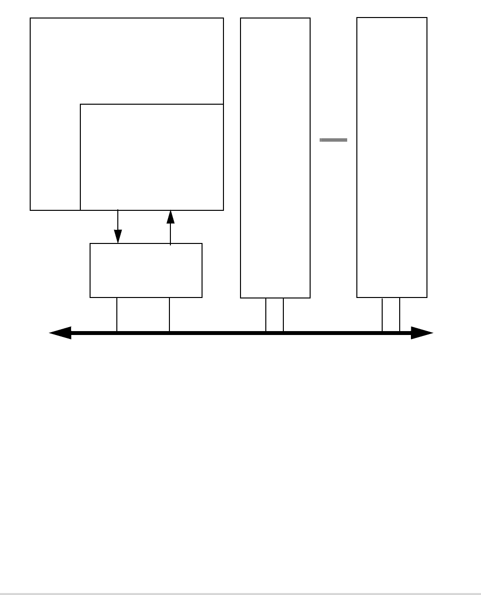
25-4 MCF5282 User’s Manual MOTOROLA
The CAN System
25.2 The CAN System
A typical CAN system is shown below in Figure 25-2.
Figure 25-2. Typical CAN system
Each CAN station is connected physically to the CAN bus through a transceiver. The
transceiver provides the transmit drive, waveshaping, and receive/compare functions
required for communicating on the CAN bus. It can also provide protection against damage
to the FlexCAN caused by a defective CAN bus or defective stations.
25.3 Message Buffers
25.3.1 Message Buffer Structure
Figure 25-3 shows the extended (29 bit) ID message buffer structure. Figure 25-4 displays
the standard (11 bit) ID message buffer structure.
CAN Bus
FlexCAN
CANRX
Transceiver
CAN Station 1 CAN Station 2 CAN Station n
CANTX
MCF5282

MOTOROLA Chapter 25. FlexCAN 25-5
Message Buffers
Figure 25-3. Extended ID Message Buffer Structure
Figure 25-4. Standard ID Message Buffer Structure
25.3.1.1 Common Fields for Extended and Standard Format Frames
Table 25-2 describes the message buffer fields that are common to both extended and
standard identifier format frames.
15–8 7–4 3–0
0x0 TIME STAMP CODE LENGTH CONTROL/STATUS
0x2 ID[28:18] SRR IDE ID[17-15] ID_HIGH
0x4 ID[14-0] RTR ID_LOW
0x6 DATA BYTE 0 DATA BYTE 1
0x8 DATA BYTE 2 DATA BYTE 3
0xA DATA BYTE 4 DATA BYTE 5
0xC DATA BYTE 6 DATA BYTE 7
0xE Reserved
15–8 7–4 3–0
0x0 TIME STAMP CODE LENGTH CONTROL/STATUS
0x2 ID[28:18] RTR 0000ID_HIGH
0x4 16-BIT TIME STAMP ID_LOW
0x6 DATA BYTE 0 DATA BYTE 1
0x8 DATA BYTE 2 DATA BYTE 3
0xA DATA BYTE 4 DATA BYTE 5
0xC DATA BYTE 6 DATA BYTE 7
0xE Reserved

25-6 MCF5282 User’s Manual MOTOROLA
Message Buffers
Table 25-2. Common Extended/Standard Format Frames
Field Description
Time Stamp Contains a copy of the high byte of the free running timer, which is captured at the beginning of the
identifier field of the frame on the CAN bus.
Code Refer to Table 25-3 and Table 25-4.
Rx Length Length (in bytes) of the Rx data stored in offset 0x6 through 0xD of the buffer. This field is written by
the FlexCAN module, copied from the data length code (DLC) field of the received frame.
Tx Length Length (in bytes) of the data to be transmitted, located in offset 0x6 through 0xD of the buffer. This
field is written by the CPU, and is used as the DLC field value. If remote transmission request (RTR))
= 1, the frame is a remote frame and will be transmitted without the data field, regardless of the value
in Tx length.
Data This field can store up to eight data bytes for a frame. For Rx frames, the data is stored as it is
received from the bus. For Tx frames, the CPU provides the data to be transmitted within the frame.
Reserved This word entry field (16 bits) should not be accessed by the CPU.
Table 25-3. Message Buffer Codes for Receive Buffers
Rx Code
Before Rx
New Frame
Description
Rx Code
After Rx
New Frame
Comment
0000 NOT ACTIVE — message buffer is not active. — —
0100 EMPTY — message buffer is active and empty. 0010 —
0010 FULL — message buffer is full.
0110
If a CPU read occurs before
the new frame, new receive
code is 0010.
0110 OVERRUN — second frame was received into a full
buffer before the CPU read the first one.
0101 1
1For transmit message buffers, upon read, the BUSY bit should be ignored.
BUSY — message buffer is now being filled with a new
receive frame. This condition will be cleared within 20
cycles.
0010 An empty buffer was filled.
001110110 A full buffer was filled.
011110110 An overrun buffer was filled.
Table 25-4. Message Buffer Codes for Transmit Buffers
RTR Initial Tx Code Description
Code After
Successful
Transmission
X 1000 Message buffer not ready for transmit. —
0 1100 Data frame to be transmitted once, unconditionally. 1000
1 1100 Remote frame to be transmitted once, and message buffer
becomes an Rx message buffer for data frames.
0100
0 1010 1
1When a matching remote request frame is detected, the code for such a message buffer is changed to be 1110.
Data frame to be transmitted only as a response to a remote
frame.
1010
0 1110 Data frame to be transmitted only once, unconditionally, and
then only as a response to remote frame.
1010

MOTOROLA Chapter 25. FlexCAN 25-7
Message Buffers
25.3.1.2 Fields for Extended Format Frames
Table 25-5 describes the message buffer fields used only for extended identifier format
frames.
25.3.1.3 Fields for Standard Format Frames
Table 25-6 describes the message buffer fields used only for standard identifier format
frames.
25.3.2 Message Buffer Memory Map
The message buffer memory map starts at an offset of 0x80 from the FlexCAN’s base
address (0x1C_0000). The 256-byte message buffer space is fully used by the 16 message
buffer structures.
Table 25-5. Extended Format Frames
Field Description
ID[28:18]/[17:15] Contains the 14 most significant bits of the extended identifier, located in the ID HIGH word of the
message buffer.
Substitute
Remote Request
(SRR)
Contains a fixed recessive bit, used only in extended format. Should be set to one by the user for
Tx buffers. It will be stored as received on the CAN bus for Rx buffers. This is a bit in the ID HIGH
word of the message buffer.
ID Extended (IDE) If extended format frame is used, this field should be set to one. If zero, standard format frame
should be used. This is a bit in the ID HIGH word of the message buffer.
ID[14:0] Bits [14:0] of the extended identifier, located in the ID LOW word of the message buffer.
Remote
Transmission
Request (RTR)
This bit is located in the least significant bit of the ID LOW word of the message buffer;
0 Data Frame
1 Remote Frame.
Table 25-6. Standard Format Frames
Field Description
ID[28:18] Contains bits [28:18] of the identifier, located in the ID HIGH word of the message buffer. The four
least significant bits in this register (corresponding to the IDE bit and ID[17:15] for an extended
identifier message) must all be written as logic zeros to ensure proper operation of the FlexCAN.
RTR Remote Transmission Request. This bit is located in the ID HIGH word of the message buffer.
0 data frame
1 remote frame.
If the FlexCAN transmits this bit as a one and receives it as a zero, an “arbitration loss” is
indicated. If the FlexCAN transmits this bit as a zero and receives it as a one, a bit error is
indicated.
If the FlexCAN transmits a value and receives a matching response, a successful bit transmission
is indicated.
16-Bit Time Stamp The 16-bit time stamp, located in the ID LOW word of the message buffer, is not needed for
standard format, and is used in a standard format buffer to store the 16-bit value of the
free-running timer. The timer value is captured at the beginning of the identifier field of the frame
on the CAN bus.

25-8 MCF5282 User’s Manual MOTOROLA
Functional Overview
Figure 25-5. FlexCAN Memory Map
25.4 Functional Overview
The FlexCAN module is flexible in that each one of its 16 message buffers (MBs) can be
assigned either as a transmit buffer or a receive buffer. Each MB, which is up to 8 bytes
long, is also assigned an interrupt flag bit that indicates successful completion of either
transmission or reception.
NOTE
Note that for both processes, the first CPU action in preparing
a MB should be to deactivate it by setting its code field to the
proper value. This requirement is mandatory to assure proper
operation.
ID_HIGH
ID_LOW
Control/Status
Reserved
8 bytes Data field
0x80-0x8F
0x82
0x84
0x86 Message Buffer 0
Message Buffer 1
Message Buffer 2
Message Buffer 15
0x8C
0x90
0xA0
0x170
Message Buffers
0x8E
0x17E
0x9E
0xAE
0xB0
0x16E
FlexCAN Base
Address Offset
Message Buffer 3
through
Message Buffer 14

MOTOROLA Chapter 25. FlexCAN 25-9
Functional Overview
25.4.1 Transmit Process
The CPU prepares or changes an MB for transmission by executing the following steps:
• Writing the Control/Status word to hold Tx MB inactive (code = 1000).
• Writing the ID_HIGH and ID_LOW words.
• Writing the Data bytes
• Writing the Control/Status word (active Code, Length)
NOTE
The first and last steps are mandatory!
Starting from the last step, this MB will participate in the internal arbitration process, which
takes place every time the CAN bus is sensed as free by the receiver or at the inter-frame
space, and there is at least one MB ready for transmission. This internal arbitration process
is intended to select the MB from which the next frame is transmitted.
When this process is over, and there is a ‘winner’ MB for transmission, the frame is
transferred to the serial message buffer (SMB) for transmission (Move Out).
While transmitting, the FlexCAN transmits up to eight data bytes, even if the DLC is bigger
in value.
At the end of the successful transmission, the value of the free-running timer (which was
captured at the beginning of the Identifier field on the CAN bus), is written into the “Time
Stamp” field in the MB, the Code field in the Control/Status word of the MB is updated and
a status flag is set in the IFLAG register.
25.4.2 Receive Process
The CPU prepares or changes an MB for frame reception by executing the following steps:
• Writing the control/status word to hold Rx MB inactive (code = 0000).
• Writing the ID_HIGH and ID_LOW words.
• Writing the control/status word to mark the Rx MB as active and empty.
NOTE
The first and last steps are mandatory!
Starting from the last step, this MB is an active receive buffer and will participate in the
internal matching process, which takes place every time the receiver receives an error-free
frame. In this process, all active receive buffers compare their ID value to the newly
received one, and if a match occurs, the frame is transferred (Move In) to the first (that is,
lowest entry) matching MB. The value of the free-running timer (which was captured at the
beginning of the Identifier field on the CAN bus) is written into the “Time Stamp” field in

25-10 MCF5282 User’s Manual MOTOROLA
Functional Overview
the MB, the ID field, data field (8 bytes at most) and the LENGTH field are stored, the Code
field is updated and a status flag is set in the IFLAG register.
The CPU should read a receive frame from its MB in the following way:
• Control/status word (mandatory—activates internal lock for this buffer).
• ID (Optional—needed only if a mask was used).
• Data field word(s).
• Free-running timer (Releases internal lock —optional).
The read of the free-running timer is not mandatory. If not executed, the MB remains
locked, unless the CPU starts the read process for another MB. Note that only a single MB
is locked at a time. The only mandatory CPU read operation is of the Control/Status word,
to assure data coherency. If the BUSY bit is set in the MB code, then the CPU should defer
until this bit is negated.
The CPU should synchronize to frame reception by the status flag for the specific MB (see
Section 25.5.10, “Interrupt Flag Register (IFLAG)”), and not by the control/status word
code field for that MB. This is because polling the control/status word may lock the MB
(see above), and the Code may change before the full frame is received into the MB.
Note that the received identifier field is always stored in the matching MB, thus the contents
of the identifier field in a MB may change if the match was due to mask.
25.4.2.1 Self-Received Frames
The FlexCAN receives self-transmitted frames if there exists a matching receive MB.
25.4.3 Message Buffer Handling
In order to maintain data coherency and proper FlexCAN operation, the CPU must obey the
rules listed in Section 25.4.1, “Transmit Process” and in Section 25.4.2, “Receive Process.”
Deactivation of a message buffer (MB) is a host action that causes that message buffer to
be excluded from FlexCAN transmit or receive processes. Any CPU write access to a
control/status word of MB structure deactivates that MB, thus excluding it from Rx/Tx
processes. Any form of CPU MB structure access within the FlexCAN (other than those
specified in Section 25.4.1, “Transmit Process” and in Section 25.4.2, “Receive Process”)
may cause the FlexCAN to behave in an unpredictable manner.
The match/arbitration processes are performed only during one period by the FlexCAN.
Once a winner or match is determined, there is no re-evaluation whatsoever, in order to
ensure that a receive frame is not lost. Two receive MBs or more that hold a matching ID
to a received frame do not assure reception in the FlexCAN if the user has deactivated the
matching MB after FlexCAN has scanned the second.

MOTOROLA Chapter 25. FlexCAN 25-11
Functional Overview
25.4.3.1 Serial Message Buffers (SMBs)
To allow double buffering of messages, the FlexCAN has two shadow buffers called serial
message buffers. These two buffers are used by the FlexCAN for buffering both received
messages and messages to be transmitted. Only one SMB is active at a time, and its function
depends upon the operation of the FlexCAN at that time. At no time does the user have
access to or visibility of these two buffers.
25.4.3.2 Transmit Message Buffer Deactivation
Any write access to the control/status word of a transmit message buffer during the process
of selecting a message buffer for transmission immediately deactivates that message buffer,
removing it from the transmission process.
If the user deactivates the transmit MB while a message is being transferred from a transmit
message buffer to a SMB the message will not be transmitted.
If the user deactivates the transmit message buffer after the message is transferred to the
SMB, the message will be transmitted, but no interrupt will be requested and the transmit
code will not be updated.
If a message buffer containing the lowest ID is deactivated while that message is
undergoing the internal arbitration process to determine which message should be sent, then
that message may not be transmitted.
25.4.3.3 Receive Message Buffer Deactivation
Any write access to the control/status word of a receive message buffer during the process
of selecting a message buffer for reception immediately deactivates that message buffer,
removing it from the reception process.
If a receive message buffer is deactivated while a message is being transferred into it, the
transfer is halted and no interrupt is requested. If this occurs, that receive message buffer
may contain mixed data from two different frames.
Data should never be written into a receive message buffer. If this is done while a message
is being transferred from an SMB, the control/status word will reflect a full or overrun
condition, but no interrupt will be requested.

25-12 MCF5282 User’s Manual MOTOROLA
Functional Overview
25.4.3.4 Locking and Releasing Message Buffers
The lock/release/busy mechanism is designed to guarantee data coherency during the
receive process. The following examples demonstrate how the lock/release/busy
mechanism will affect FlexCAN operation.
1. Reading a control/status word of a message buffer triggers a lock for that message
buffer. A new received message frame which matches the message buffer cannot be
written into this message buffer while it is locked.
2. To release a locked message buffer, the CPU either locks another message buffer
(by reading its control/status word) or globally releases any locked message buffer
(by reading the free-running timer).
3. If a receive frame with a matching ID is received during the time the message
buffer is locked, the receive frame will not be immediately transferred into that
message buffer, but will remain in the SMB. There is no indication when this
occurs.
4. When a locked message buffer is released, if a frame with a matching identifier
exists within the SMB, then this frame will be transferred to the matching message
buffer.
5. If two or more receive frames with matching IDs are received while a message
buffer with a matching ID is locked, the last received frame with that ID is kept
within the serial message buffer, while all preceding ones are lost. There is no
indication when this occurs.
6. If the user reads the control/status word of a receive message buffer while a frame
is being transferred from a serial message buffer, the BUSY code will be indicated.
The user should wait until this code is cleared before continuing to read from the
message buffer to ensure data coherency. In this situation, the read of the
control/status word will not lock the message buffer.
Polling the control/status word of a receive message buffer can lock it, preventing a
message from being transferred into that buffer. If the control/status word of a receive
message buffer is read, it should then be followed by a read of the control/status word of
another buffer, or by reading the free-running timer, to ensure that the locked buffer is
unlocked.
25.4.4 Remote Frames
The remote frame is a message frame which is transmitted to request a data frame. The
FlexCAN can be configured to transmit a data frame automatically in response to a remote
frame, or to transmit a remote frame and then wait for the responding data frame to be
received.
When transmitting a remote frame, the user initializes a message buffer as a transmit
message buffer with the RTR bit set to one. Once this remote frame is transmitted

MOTOROLA Chapter 25. FlexCAN 25-13
Functional Overview
successfully, the transmit message buffer automatically becomes a receive message buffer,
with the same ID as the remote frame which was transmitted.
When a remote frame is received by the FlexCAN, the remote frame ID is compared to the
IDs of all transmit message buffers programmed with a code of 1010. If there is an exact
matching ID, the data frame in that message buffer is transmitted. If the RTR bit in the
matching transmit message buffer is set, the FlexCAN will transmit a remote frame as a
response.
A received remote frame is not stored in a receive message buffer. It is only used to trigger
the automatic transmission of a frame in response. The mask registers are not used in
remote frame ID matching. All ID bits (except RTR) of the incoming received frame must
match for the remote frame to trigger a response transmission.
25.4.5 Overload Frames
Overload frame transmissions are not initiated by the FlexCAN unless certain conditions
are detected on the CAN bus. These conditions include:
• Detection of a dominant bit in the first or second bit of intermission.
• Detection of a dominant bit in the seventh (last) bit of the end-of-frame (EOF) field
in receive frames.
• Detection of a dominant bit in the eighth (last) bit of the error frame delimiter or
overload frame delimiter.
25.4.6 Time Stamp
The value of the free-running 16-bit timer is sampled at the beginning of the identifier field
on the CAN bus. For a message being received, the time stamp will be stored in the time
stamp entry of the receive message buffer at the time the message is written into that buffer.
For a message being transmitted, the time stamp entry will be written into the transmit
message buffer once the transmission has completed successfully.
The free-running timer can optionally be reset upon the reception of a frame into message
buffer 0. This feature allows network time synchronization to be performed.
25.4.7 Listen-Only Mode
In listen-only mode, the FlexCAN module is able to receive messages without giving an
acknowledgment. Whenever the module enters this mode the status of the Error Counters
is frozen and the FlexCAN module operates like in error passive mode. Since the module
does not influence the CAN bus in this mode the host device is capable of functioning like
a monitor or for automatic bit-rate detection.

25-14 MCF5282 User’s Manual MOTOROLA
Functional Overview
25.4.8 Bit Timing
The FlexCAN module uses three 8-bit registers to set up the bit timing parameters required
by the CAN protocol. Control registers 1 and 2 (CANCTRL1, CANCTRL2) contain the
PROPSEG, PSEG1, PSEG2, and the RJW fields which allow the user to configure the bit
timing parameters. The prescaler divide register (PRESDIV) allows the user to select the
ratio used to derive the S-clock from the system clock. The time quanta clock operates at
the S-clock frequency. Table 25-7 provides examples of system clock, CAN bit rate, and
S-clock bit timing parameters.
25.4.8.1 Configuring the FlexCAN Bit Timing
The following considerations must be observed when programming bit timing functions.
• If the programmed PRESDIV value results in a single system clock per one time
quantum, then the PSEG2 field in CANCTRL1 register should not be programmed
to zero.
• If the programmed PRESDIV value results in a single system clock per one time
quantum, then the information processing time (IPT) equals three time quanta,
otherwise it equals two time quanta. If PSEG2 equals two, then the FlexCAN
transmits one time quantum late relative to the scheduled sync segment.
• If the prescaler and bit timing control fields are programmed to values that result in
fewer than ten system clock periods per CAN bit time and the CAN bus loading is
100%, anytime the rising edge of a start-of-frame (SOF) symbol transmitted by
another node occurs during the third bit of the intermission between messages, the
FlexCAN may not be able to prepare a message buffer for transmission in time to
begin its own transmission and arbitrate against the message which transmitted the
early SOF.
• The FlexCAN bit time must be programmed to be greater than or equal to nine
system clocks, or correct operation is not guaranteed.
Table 25-7. Examples of System Clock/CAN Bit-Rate/S-Clock
System Clock
Freq (Mhz)
Can bit-rate
(Mhz)
Possible
S-Clock Freq
(Mhz)
Possible
number of
time-quanta/bit
Pre-Scaler
programed
value + 1
Comments
48 1 8,12,24 8,12,24 3,2,1
Min 8 time-quanta
Max 25 time-quanta
40 1 10,20 10,20 2,1
32 1 8,16 8,16 2,1
48 0.125 1,1.5,2,3 8,12,16,24 24,16,12,8
40 0.125 1,2,2.5 8,16,20 20,10,8
32 0.125 1,2 8,16 16,8

MOTOROLA Chapter 25. FlexCAN 25-15
Functional Overview
25.4.9 FlexCAN Error Counters
There are two error counters in the FlexCAN: transmit error counter (TXECTR), and
receive error counter (RXCTR). The rules for increasing and decreasing these counters are
described in the CAN protocol, and are fully implemented in the FlexCAN. Each counter
comprises the following:
• 8 bit up/down counter
• Increment by 8 (Rx_Err_Counter also by 1)
• Decrement by 1
• Avoid decrement when equal to zero
• Rx_Err_Counter preset to a value 119 ≤ x ≤ 127
• Value after reset = zero
• Detect values for Error Passive, Bus Off and Error Active transitions and for alerting
the host.
Both counters are read only (except for Test/Freeze/Halt modes).
The FlexCAN responds to any bus state as described in the protocol, e.g. transmit error
active or error passive flag, delay its transmission start time (Error Passive) and avoid any
influence on the bus when in Bus Off state. The following are the basic rules for FlexCAN
bus state transitions:
• If the value of TXCTR or RXCTR increases to be greater than or equal to 128, the
FCS field in the error status register is updated to reflect it (set Error Passive state).
• If the FlexCAN state is Error Passive, and either TXCTR counter or RXCTR then
decrements to a value less than or equal to 127 while the other already satisfies this
condition, the ESTAT[FCS] field is updated to reflect it (set Error Active state).
• If the value of the TXCTR increases to be greater than 255, the ESTAT[FCS] field
is updated to reflect it (set Bus Off state) and an interrupt may be issued. The value
of TXCTR is then reset to zero.
• If the FlexCAN state is Bus_Off, then TXCTR, together with an internal counter are
cascaded to count the 128 occurrences of 11 consecutive recessive bits on the bus.
Hence, TXCTR is reset to zero, and counts in a manner where the internal counter
counts 11 such bits and then wraps around while incrementing the TXCTR. When
TXCTR reaches the value of 128, ESTAT[FCS] is updated to be Error Active, and
both error counters are reset to zero. At any instance of dominant bit following a
stream of less than 11 consecutive recessive bits, the internal counter resets itself to
zero, but does NOT affect the TXCTR value.
• If during system start-up, only one node is operating, then its TXCTR increases with
each message it’s trying to transmit as a result of ACK_ERROR. A transition to bus
state Error Passive should be executed as described, while this device never enters
the Bus_Off state.

25-16 MCF5282 User’s Manual MOTOROLA
Functional Overview
• If the RXCTR increases to a value greater than 127, it is no longer incremented, even
if more errors are detected while being a receiver. At the next successful message
reception, the counter is set to a value between 119 and 127, in order to return to
Error Active state.
25.4.10 FlexCAN Initialization Sequence
Initialization of the FlexCAN includes the initial configuration of the message buffers and
configuration of the CAN communication parameters following a reset, as well as any
reconfiguration which may be required during operation. The following is a generic
initialization sequence for the FlexCAN:
1. Initialize all operation modes
a) Initialize the transmit and receive pin modes in control register 0
(CANCTRL0).
b) Initialize the bit timing parameters PROPSEG, PSEGS1, PSEG2, and RJW
in control registers 1 and 2 (CANCTRL[1:2]).
c) Select the S-clock rate by programming the PRESDIV register.
d) Select the internal arbitration mode (LBUF bit in CANCTRL1).
2. Initialize message buffers
a) The control/status word of all message buffers must be written either as an
active or inactive message buffer.
b) All other entries in each message buffer should be initialized as required.
3. Initialize mask registers for acceptance mask as needed
4. Initialize FlexCAN interrupt handler
a) Initialize the interrupt configuration register (CANICR) with a specific request
level and vector base address.
b) Set the required mask bits in the IMASK register (for all message buffer
interrupts), in CANCTRL0 (for bus off and error interrupts), and in CANMCR
for the WAKE interrupt.
5. Negate the HALT bit in the module configuration register
a) At this point, the FlexCAN will attempt to synchronize with the CAN bus.
NOTE
In both the transmit and receive processes, the first action in
preparing a message buffer should be to deactivate the buffer
by setting its code field to the proper value. This requirement is
mandatory to assure data coherency.

MOTOROLA Chapter 25. FlexCAN 25-17
Functional Overview
25.4.11 Special Operating Modes
25.4.11.1 Debug Mode
Debug mode is entered by setting the HALT bit in the CANMCR, or by assertion of the
BKPT line. In both cases, the FRZ bit in CANMCR must also be set to allow HALT or
BKPT to place the FlexCAN in debug mode.
Once entry into debug mode is requested, the FlexCAN waits until an intermission or idle
condition exists on the CAN bus, or until the FlexCAN enters the error passive or bus off
state. Once one of these conditions exists, the FlexCAN waits for the completion of all
internal activity. When this happens, the following events occur:
• The FlexCAN stops transmitting/receiving frames.
• The prescaler is disabled, thus halting all CAN bus communication.
• The FlexCAN ignores its Rx pins and drives its Tx pins as recessive.
• The FlexCAN loses synchronization with the CAN bus and the NOTRDY and
FRZACK bits in CANMCR are set.
• The CPU is allowed to read and write the error counter registers.
After engaging one of the mechanisms to place the FlexCAN in debug mode, the user must
wait for the FRZACK bit to be set before accessing any other registers in the FlexCAN,
otherwise unpredictable operation may occur.
To exit debug mode, the BKPT line must be negated or the HALT bit in CANMCR must be
cleared.
Once debug mode is exited, the FlexCAN will resynchronize with the CAN bus by waiting
for 11 consecutive recessive bits before beginning to participate in CAN bus
communication.
25.4.11.2 Low-Power Stop Mode for Power Saving
Before entering low-power stop mode, the FlexCAN will wait for the CAN bus to be in an
idle state, or for the third bit of intermission to be recessive. The FlexCAN then waits for
the completion of all internal activity (except in the CAN bus interface) to be complete.
Afterwards, the following events occur:
• The FlexCAN shuts down its clocks, stopping most internal circuits, thus achieving
maximum power savings.
• The bus interface unit continues to operate, allowing the CPU to access the module
configuration register.
• The FlexCAN ignores its Rx pins and drives its Tx pins as recessive.
• The FlexCAN loses synchronization with the CAN bus, and the STOPACK and
NOTRDY bits in the module configuration register are set.

25-18 MCF5282 User’s Manual MOTOROLA
Functional Overview
To exit low-power stop mode:
• Reset the FlexCAN either by asserting RSTI or by setting the SOFTRST bit
CANMCR.
• Clear the STOP bit in CANMCR.
• The FlexCAN module can optionally exit low-power stop mode via the self-wake
mechanism. If the SELFWAKE bit in CANMCR was set at the time the FlexCAN
entered stop mode, then upon detection of a recessive to dominant transition on the
CAN bus, the FlexCAN clears the STOP bit in CANMCR and its clocks begin
running.
When in low-power stop mode, a recessive to dominant transition on the CAN bus causes
the WAKEINT bit in the error and status register (ESTAT) to be set. This event can generate
an interrupt if the WAKEMSK bit in CANMCR is set.
Consider the following notes regarding low-power stop mode:
• When the self-wake mechanism activates, the FlexCAN tries to receive the frame
that woke it up. (It assumes that the dominant bit detected is a start-of-frame bit). It
will not arbitrate for the CAN bus at this time.
• The CPU should disable all interrupts in the FlexCAN before entering low-power
stop mode. Otherwise it may be interrupted while in STOP mode upon a non
wake-up condition; If desired, the WAKEMASK bit should be set to enable the
WAKEINT.
• If the STOP bit is set while the FlexCAN is in the bus off state, then the FlexCAN
will enter low-power stop mode and stop counting recessive bit times. The count
will continue when STOP is cleared.
• To place the FlexCAN in low-power stop mode with the self-wake mechanism
engaged, write to CANMCR with both STOP and SELFWAKE set, then wait for the
FlexCAN to set the STOPACK bit.
• To take the FlexCAN out of low-power stop mode when the self-wake mechanism
is enabled, write to CANMCR with both STOP and SELFWAKE clear, then wait for
the FlexCAN to clear the STOPACK bit.
• The SELFWAKE bit should not be set after the FlexCAN has already entered
low-power stop mode.
• If both STOP and SELFWAKE are set and a recessive to dominant edge
immediately occurs on the CAN bus, the FlexCAN may never set the STOPACK bit,
and the STOP bit will be cleared.
• To prevent old frames from being sent when the FlexCAN awakes from low-power
stop mode via the self-wake mechanism, disable all transmit sources, including
transmit buffers configured for remote request responses, before placing the
FlexCAN in low-power stop mode.

MOTOROLA Chapter 25. FlexCAN 25-19
Functional Overview
• If the FlexCAN is in debug mode when the STOP bit is set, the FlexCAN will
assume that debug mode should be exited. As a result, it will try to synchronize with
the CAN bus, and only then will it await the conditions required for entry into
low-power stop mode.
• Unlike other modules, the FlexCAN does not come out of reset in low-power stop
mode. The basic FlexCAN initialization procedure (see Section 25.4.10, “FlexCAN
Initialization Sequence”) should be executed before placing the module in
low-power stop mode.
• If the FlexCAN is in low-power stop mode with the self-wake mechanism engaged
and is operating with a single system clock per time quantum, there can be extreme
cases in which FlexCAN wake-up on recessive to dominant edge may not conform
to the CAN protocol. FlexCAN synchronization will be shifted one time quantum
from the wake-up event. This shift lasts until the next recessive to dominant edge,
which resynchronizes the FlexCAN to be in conformance with the CAN protocol.
The same holds true when the FlexCAN is in auto-power save mode and awakens
on a recessive to dominant edge.
25.4.11.3 Auto-Power Save Mode
Auto-power save mode enables normal operation with optimized power savings. Once the
auto-power save (APS) bit in CANMCR is set, the FlexCAN looks for a set of conditions
in which there is no need for its clocks to be running. If these conditions are met, the
FlexCAN stops its clocks, thus saving power. The following conditions will activate
auto-power save mode.
• No Rx/Tx frame in progress.
• No transfer of Rx/Tx frames to and from an SMB, and no Tx frame awaiting
transmission in any message buffer.
• No CPU access to the FlexCAN module.
• The FlexCAN is not in debug mode, low-power stop mode, or the bus off state.
While its clocks are stopped, if the FlexCAN senses that any one of the aforementioned
conditions is no longer true, it restarts its clocks. The FlexCAN then continues to monitor
these conditions and stops/restarts its clocks accordingly.
25.4.12 Interrupts
The module can generate up to 19 interrupt sources (16 interrupts due to message buffers
and 3 interrupts due to Bus-off, Error and Wake-up). Each one of the message buffers can
be an interrupt source, if its corresponding IMASK bit is set.
There is no distinction between Tx and Rx interrupts for a particular buffer, under the
assumption that the buffer is initialized for either transmission or reception, and thus its

25-20 MCF5282 User’s Manual MOTOROLA
Programmer’s Model
interrupt routine can be fixed at compilation time. Each of the buffers is assigned a bit in
the IFLAG register. The bit is set when the corresponding buffer completes a successful
transmission or reception, and cleared when the CPU reads the interrupt flag register
(IFLAG) while the associated bit is set, and then writes it back as ‘1’ (and no new event of
the same type occurs between the read and the write actions).
The other 3 interrupt sources (Bus-off, Error and Wake-up) act in the same way, and are
located in the Error & Status register. The Bus-off and Error interrupt mask bits are located
in the CANCTRL0 register, and the Wake-up interrupt mask bit is located in the CANMCR.
25.5 Programmer’s Model
This section describes the registers in the FlexCAN module.
NOTE
The FlexCAN has no hard-wired protection against invalid
bit/field programming within its registers. Specifically, no
protection is provided if the programming does not meet CAN
protocol requirements.
Programming the FlexCAN control registers is typically done during system initialization,
prior to the FlexCAN becoming synchronized with the CAN bus. The configuration
registers can be changed after synchronization by halting the FlexCAN module. This is
done when the user sets the HALT bit in the FlexCAN module configuration register
(CANMCR). The FlexCAN responds by setting the CANMCR[NOTRDY] bit.
Additionally, the control registers can be modified while the MCU is in background debug
mode.
25.5.1 CAN Module Configuration Register (CANMCR)
Table 25-8 describes the CANMCR fields.
15 14 13 12 11 10 9 8
Field STOP FRZ — HALT NOTRDY WAKEMSK SOFTRST FRZACK
Reset 0101_1001
R/W R/W
76543 0
Field SUPV SELFWAKE APS STOPACK —
Reset 1000_0000
R/W R/W
Address IPSBAR + 0x1C_0000
Figure 25-6. CAN Module Configuration Register (CANMCR)

MOTOROLA Chapter 25. FlexCAN 25-21
Programmer’s Model
Table 25-8. CANMCR Field Descriptions
Bits Name Description
15 STOP
Low-power stop mode enable. The STOP bit may only be set by the CPU. It may be cleared either
by the CPU or by the FlexCAN, if the SELFWAKE bit is set.
0 Enable FlexCAN clocks
1 Disable FlexCAN clocks
14 FRZ
FREEZE assertion response. When FRZ = 1, the FlexCAN can enter debug mode when the BKPT
line is asserted or the HALT bit is set. Clearing this bit field causes the FlexCAN to exit debug
mode. Refer to Section 25.4.11.1, “Debug Mode” for more information.
0 FlexCAN ignores the BKPT signal and the HALT bit in the module configuration register.
1 FlexCAN module enabled to enter debug mode.
13 — Reserved
12 HALT
Halt FlexCAN S-Clock. Setting the HALT bit has the same effect as assertion of the BKPT signal
on the FlexCAN without requiring that BKPT be asserted. This bit is set to one after reset. It should
be cleared after initializing the message buffers and control registers. FlexCAN message buffer
receive and transmit functions are inactive until this bit is cleared.
When HALT is set, write access to certain registers and bits that are normally read-only is allowed.
0 The FlexCAN operates normally
1 FlexCAN enters debug mode if FRZ = 1
11 NOTRDY
FlexCAN not ready. This bit indicates that the FlexCAN is either in low-power stop mode or debug
mode. This bit is read-only and is set only when the FlexCAN enters low-power stop mode or
debug mode. It is cleared once the FlexCAN exits either mode, either by synchronization to the
CAN bus or by the self-wake mechanism.
0 FlexCAN has exited low-power stop mode or debug mode.
1 FlexCAN is in low-power stop mode or debug mode.
10 WAKEMSK
Wakeup interrupt mask. The WAKEMSK bit enables wake-up interrupt requests.
0 Wake up interrupt is disabled.
1 Wake up interrupt is enabled.
9SOFTRST
Soft reset. When this bit is asserted, the FlexCAN resets its internal state machines (sequencer,
error counters, error flags, and timer) and the host interface registers (CANMCR, CANICR,
CANTCR, IMASK, and IFLAG).
The configuration registers that control the interface with the CAN bus are not changed (CAN-
CTRL[0:2] and PRESDIV). Message buffers and receive message masks are also not changed.
This allows SOFTRST to be used as a debug feature while the system is running.
Setting SOFTRST also clears the STOP bit in CANMCR.
After setting SOFTRST, allow one complete bus cycle to elapse for the internal FlexCAN circuitry
to completely reset before executing another access to CANMCR.
The FlexCAN clears this bit once the internal reset cycle is completed.
0 Soft reset cycle completed
1 Soft reset cycle initiated
8FRZACK
FlexCAN disable. When the FlexCAN enters debug mode, it sets the FRZACK bit. This bit should
be polled to determine if the FlexCAN has entered debug mode. When debug mode is exited, this
bit is negated once the FlexCAN prescaler is enabled. This is a read-only bit.
0 The FlexCAN has exited debug mode and the prescaler is enabled.
1 The FlexCAN has entered debug mode, and the prescaler is disabled.

25-22 MCF5282 User’s Manual MOTOROLA
Programmer’s Model
25.5.2 FlexCAN Control Register 0 (CANCTRL0)
Table 25-9 describes the CANCTRL0 fields.
7SUPV
Supervisor/user data space. The SUPV bit places the FlexCAN registers in either supervisor or
user data space.
0 Registers with access controlled by the SUPV bit are accessible in either user or supervisor
privilege mode.
1 Registers with access controlled by the SUPV bit are restricted to supervisor mode.
6SELF-
WAKE
Self wake enable. This bit allows the FlexCAN to wake up when bus activity is detected after the
STOP bit is set. If this bit is set when the FlexCAN enters low-power stop mode, the FlexCAN will
monitor the bus for a recessive to dominant transition. If a recessive to dominant transition is
detected, the FlexCAN immediately clears the STOP bit and restarts its clocks.
If a write to CANMCR with SELFWAKE set occurs at the same time a recessive-to-dominant edge
appears on the CAN bus, the bit will not be set, and the module clocks will not stop. The user
should verify that this bit has been set by reading CANMCR. Refer to Section 25.4.11.2,
“Low-Power Stop Mode for Power Saving” for more information on entry into and exit from
low-power stop mode.
0 Self wake disabled.
1 Self wake enabled.
5 APS
Auto-power save. The APS bit allows the FlexCAN to automatically shut off its clocks to save
power when it has no process to execute, and to automatically restart these clocks when it has a
task to execute without any CPU intervention.
0 Auto-power save mode disabled; clocks run normally.
1 Auto-power save mode enabled; clocks stop and restart as needed.
4 STOPACK
Stop acknowledge. When the FlexCAN is placed in low-power stop mode and shuts down its
clocks, it sets the STOPACK bit. This bit should be polled to determine if the FlexCAN has entered
low-power stop mode. When the FlexCAN exits low-power stop mode, the STOPACK bit is cleared
once the FlexCAN’s clocks are running.
0 The FlexCAN is not in low-power stop mode and its clocks are running.
1 The FlexCAN has entered low-power stop mode and its clocks are stopped
3–0 — Reserved, should be cleared.
76543210
Field BOFFMSK ERRMSK — RXMODE TXMODE
Reset 0000_0000
R/W R/W
Address IPSBAR + 0x1C_0006
Figure 25-7. FlexCAN Control Register 0 (CANCTRL0)
Table 25-8. CANMCR Field Descriptions (continued)
Bits Name Description
MOTOROLA Chapter 25. FlexCAN 25-23
Programmer’s Model
25.5.3 FlexCAN Control Register 1 (CANCTRL1)
Table 25-11 describes the CANCTRL1 fields.
Table 25-9. CANCTRL0 Field Descriptions
Bits Name Description
7BOFFMSK
Bus off interrupt mask. The BOFF MASK bit provides a mask for the bus off interrupt.
0 Bus off interrupt disabled.
1 Bus off interrupt enabled.
6 ERRMSK
Error interrupt mask. The ERRMSK bit provides a mask for the error interrupt.
0 Error interrupt disabled.
1 Error interrupt enabled.
5–3 — Reserved
2RXMODE
Receive pin configuration control. This bit determines the polarity of the CANRX pin.
0 A logical ‘0’ is interpreted as a dominant bit; a logical ‘1’ is interpreted as a recessive bit.
1 A logical ‘1’ is interpreted as a dominant bit; a logical ‘0’ is interpreted as a recessive bit.
1–0 TXMODE Transmit pin configuration control. This bit field controls the configuration of the CANTX pin. See
Table 25-10.
Table 25-10. Transmit Pin Configuration
TXMODE[1:0] Transmit Pin Configuration
00 Full CMOS 1; positive polarity (CANTX= 0 is a dominant level)
1Full CMOS drive indicates that both dominant and recessive levels are driven by the chip.
01 Full CMOS1; negative polarity (CANTX = 1 is a dominant level)
1X Open drain 2; positive polarity
2Open drain drive indicates that only a dominant level is driven by the chip. During a recessive
level, the CANTX pin is disabled (three stated), and the electrical level is achieved by external
pull-up/pull-down devices. The assertion of both Tx mode bits causes the polarity inversion to
be cancelled (open drain mode forces the polarity to be positive).
76543210
Field SAMP — TSYNC LBUF LOM PROPSEG
Reset 0000_0000
R/W R/W
Address IPSBAR + 0x1C_0007
Figure 25-8. FlexCAN Control Register 1 (CANCTRL1)

25-24 MCF5282 User’s Manual MOTOROLA
Programmer’s Model
25.5.4 Prescaler Divide Register (PRESDIV)
Table 25-12 describes the PRESDIV fields.
Table 25-11. CANCTRL1 Field Descriptions
Bits Name Description
7 SAMP
Sampling mode. The SAMP bit determines whether the FlexCAN module will sample each received
bit one time or three times to determine its value.
0 One sample, taken at the end of phase buffer segment 1, is used to determine the value of the
received bit.
1 Three samples are used to determine the value of the received bit. The samples are taken at the
normal sample point and at the two preceding periods of the S-clock.
6 — Reserved, should be cleared.
5 TSYNC
Timer synchronize mode. The TSYNC bit enables the mechanism that resets the free-running timer
each time a message is received in Message Buffer 0. This feature provides the means to synchro-
nize multiple FlexCAN stations with a special “SYNC” message (global network time).
0 Timer synchronization disabled.
1 Timer synchronization enabled.
Note: there can be a bit clock skew of four to five counts between different FlexCAN modules that
are using this feature on the same network.
4LBUF
Lowest buffer transmitted first. The LBUF bit defines the transmit-first scheme.
0 Message buffer with lowest ID is transmitted first.
1 Lowest numbered buffer is transmitted first.
3LOM
Listen Only Mode. In this mode the FlexCAN is able to receive messages without giving an acknowl-
edgment or being active on the bus.
0 Regular operation (listen only mode off).
1 Enable listen only mode.
2–0 PROPSEG
Propagation segment time. PROPSEG defines the length of the propagation segment in the bit
time. The valid programmed values are 0 to 7. The propagation segment time is calculated as
follows:
Propagation Segment Time = (PROPSEG + 1) Time Quanta
where
1 Time Quantum = 1 Serial Clock (S-Clock) Period
7 0
Field PRES_DIV
Reset 0000_0000
R/W R/W
Address IPSBAR + 0x1C_0008
Figure 25-9. Prescaler Divide Register (PRESDIV)

MOTOROLA Chapter 25. FlexCAN 25-25
Programmer’s Model
25.5.5 FlexCAN Control Register 2 (CANCTRL2)
Table 25-13 describes the CANCTRL2 fields.
Table 25-12. PRESDIV Field Descriptions
Bits Name Description
7–0 PRES_DIV Prescaler divide factor. PRESDIV determines the ratio between the system clock frequency and
the serial clock (S-clock). The S-clock is determined by the following calculation:
The reset value of PRESDIV is 0x00, which forces the S-clock to default to the same frequency
as the system clock. The valid programmed values are 0 through 255. See Section 25.4.8, “Bit
Timing” for more information.
765 32 0
Field RJW PSEG1 PSEG2
Reset 0000_0000
R/W R/W
Address IPSBAR + 0x1C_0009
Figure 25-10. FlexCAN Control Register 2 (CANCTRL2)
Table 25-13. CANCTRL2 Field Descriptions
Bits Name Description
7–6 RJW Resynchronization jump width. The RJW field defines the maximum number of time quanta a bit time
may be changed during resynchronization. The valid programmed values are 0 through 3.
The resynchronization jump width is calculated as follows:
Resynchronizaton Jump Width = (RJW + 1) Time Quanta
5–3 PSEG1 PSEG1[2:0] — Phase buffer segment 1. The PSEG1 field defines the length of phase buffer segment
1 in the bit time. The valid programmed values are 0 through 7.
The length of phase buffer segment 1 is calculated as follows:
Phase Buffer Segment 1 = (PSEG1 + 1) Time Quanta
2–0 PSEG2 PSEG2 — Phase Buffer Segment 2. The PSEG2 field defines the length of phase buffer segment 2 in
the bit time. The valid programmed values are 0 through 7.
The length of phase buffer segment 2 is calculated as follows:
Phase Buffer Segment 2 = (PSEG2 + 1) Time Quanta
S-clock
fsys
2 PRESDIV + 1()
---------------------------------------------=

25-26 MCF5282 User’s Manual MOTOROLA
Programmer’s Model
25.5.6 Free Running Timer (TIMER)
Table 25-14 describes the TIMER fields.
25.5.7 Rx Mask Registers
These registers are used as acceptance masks for received frame IDs. 3 masks are defined:
A global mask, used for Rx buffers 0-13, and 2 more separate masks for buffers 14 and 15.
Mask bit = 0: The corresponding incoming ID bit is “don’t care”.
Mask bit = 1: The corresponding ID bit is checked against the incoming ID bit, to see if a
match exists.
Note that these masks are used both for Standard and Extended ID formats. The value of
mask registers should NOT be changed while in normal operation, as locked frames which
matched a MB through a mask, may be transferred into the MB (upon release) but may no
longer match.
15 0
Field TIMER
Reset 0000_0000_0000_0000
R/W R/W
Address IPSBAR + 0x1C_000A
Figure 25-11. Free Running Timer (TIMER)
Table 25-14. TIMER Field Descriptions
Bits Name Description
15–0 TIMER The free running timer counter can be read and written by the CPU. The timer starts from zero after
reset, counts linearly to 0xFFFF, and wraps around.
The timer is clocked by the FlexCAN bit-clock. During a message, it increments by one for each bit that
is received or transmitted. When there is no message on the bus, it increments at the nominal bit rate.
The timer value is captured at the beginning of the identifier field of any frame on the CAN bus. The
captured value is written into the “time stamp” entry in a message buffer after a successful reception
or transmission of a message.
Table 25-15. Mask examples for Normal/Extended Messages
Base ID
ID28.................ID18
I
D
E
Extended ID
ID17......................................ID0 Match
MB2-Id 1 1 1 1 1 1 1 1 0 0 0 0
MB3-Id 1 1 1 1 1 1 1 1 0 0 0 1 0 1 0 1 0 1 0 1 0 1 0 1 0 1 0 1 0 1
MB4-Id 0 0 0 0 0 0 1 1 1 1 1 0
MB5-Id 0 0 0 0 0 0 1 1 1 0 1 1 0 1 0 1 0 1 0 1 0 1 0 1 0 1 0 1 0 1
MOTOROLA Chapter 25. FlexCAN 25-27
Programmer’s Model
25.5.7.1 Receive Mask Registers (RXGMASK, RX14MASK, RX15MASK)
The Rx global mask register (RXGMASK) is composed of 4 bytes. The mask bits are
applied to all Rx-Identifiers excluding Rx-buffers 14-15, that have their specific Rx-mask
registers (RX14MASK and RX15MASK).
MB14-Id 1 1 1 1 1 1 1 1 0 0 0 1 0 1 0 1 0 1 0 1 0 1 0 1 0 1 0 1 0 1
Rx_Global_Mas
k
1 1 1 1 1 1 1 1 1 1 0 1 1 1 1 1 1 1 0 0 0 0 0 0 0 0 0 0 1
Rx_Msg in 1 1 1 1 1 1 1 1 0 0 1 1 0 1 0 1 0 1 0 1 0 1 0 1 0 1 0 1 0 1 3 1
Rx_Msg in 1 1 1 1 1 1 1 1 0 0 1 0 2 2
Rx_Msg in 1 1 1 1 1 1 1 1 0 0 1 1 0 1 0 1 0 1 0 1 0 1 0 1 0 1 0 1 0 0 3
Rx_Msg in 0 1 1 1 1 1 1 1 0 0 0 0 4
Rx_Msg in 0 1 1 1 1 1 1 1 0 0 0 1 0 1 0 1 0 1 0 1 0 1 0 1 0 1 0 1 0 1 5
Rx_14_Mask 0 1 1 1 1 1 1 1 1 1 1 1 1 1 1 1 1 1 0 0 0 0 0 0 0 0 0 0 0
Rx_Msg in 1 0 1 1 1 1 1 1 0 0 0 1 0 1 0 1 0 1 0 1 0 1 0 1 0 1 0 1 0 1 6
Rx_Msg in 0 1 1 1 1 1 1 1 0 0 0 1 0 1 0 1 0 1 0 1 0 1 0 1 0 1 0 1 0 1 14 7
1Match for Extended Format (MB3).
2Match for Standard Format. (MB2).
3Un-Match for MB3 because of ID0.
4 Un-Match for MB2 because of ID28.
5Un-Match for MB3 because of ID28, Match for MB14.
6Un-Match for MB14 because of ID27.
7Match for MB14.
31 21 20 19 18 17 16
Field MID[28:18] — MID[17:15]
Reset 1111_1111_1110_1111
R/W R/W
15 10
Field MID[14:0] —
Reset 1111_1111_1111_1110
R/W R/W
Address IPSBAR + 0x1C_0010 (RXGMASK), 0x1C_0014 (RX14MASK), 0x1C_0018 (RX15MASK)
Figure 25-12. Rx Mask Registers (RXGMASK, RX14MASK, and RX15MASK)
Table 25-15. Mask examples for Normal/Extended Messages (continued)
Base ID
ID28.................ID18
I
D
E
Extended ID
ID17......................................ID0 Match

25-28 MCF5282 User’s Manual MOTOROLA
Programmer’s Model
25.5.8 FlexCAN Error and Status Register (ESTAT)
ESTAT reflects various error conditions, some general status of the device, and is the source
of three interrupts to the host. The reported error conditions (bits 15:10) are those occurred
since the last time the host read this register. The read action clears these bits to 0.
All the bits in this register are read only, except for BOFF_INT, WAKE_INT and
ERR_INT, which are interrupt sources and can be written by the host to ‘0’.
Section 25.4.12, “Interrupts.”
Table 25-17 describes the ESTAT fields.
Table 25-16. RXGMASK, RX14MASK, and RX15MASK Field Descriptions
Bits Name Description
31–21 MID Mask ID. MID[28:18] are used to mask standard or extended format frames.
0 corresponding incoming ID bit is “don’t care”.
1 corresponding ID bit is checked against the incoming ID bit, to see if a match exists.
20 — Reserved. The IDE bit of a received frame is always compared. Its location in the mask (bit 19) is
always 1, regardless of any CPU write to this bit.
19 — Reserved. The RTR/SRR bit of a received frame is never compared to the corresponding bit in the
MB ID field. Note, however, that remote request frames (RTR = 1) are never received into MBs. RTR
mask bits locations in the mask (bits 20 and 0) are always read as ’0’, regardless of any CPU write
to these bits.
18–1 MID Mask ID. MID[17:0] are only used to mask extended format frames.
0 corresponding incoming ID bit is “don’t care”.
1 corresponding ID bit is checked against the incoming ID bit, to see if a match exists.
0 — Reserved. The RTR/SRR bit of a received frame is never compared to the corresponding bit in the
MB ID field. Note, however, that remote request frames (RTR = 1) are never received into MBs. RTR
mask bits locations in the mask (bits 20 and 0) are always read as ’0’, regardless of any CPU write
to these bits.
15 14 13 12 11 10 9 8
Field BITERR ACKERR CRCERR FORMERR STUFFERR TXWARN RXWARN
Reset 0000_0000
R/W R
76543120
Field IDLE TX/RX FCS — BOFFINT ERRINT WAKEINT
Reset 0000_0000
R/W R R/W
Address IPSBAR + 0x1C_0020
Figure 25-13. FlexCAN Error and Status Register (ESTAT)

MOTOROLA Chapter 25. FlexCAN 25-29
Programmer’s Model
Table 25-17. ESTAT Field Descriptions
Bits Name Description
15–14 BITERR Transmit bit error. The BITERR[1:0] field is used to indicate when a transmit bit error occurs.
00 No transmit bit error
01 At least one bit sent as dominant was received as recessive
10 At least one bit sent as recessive was received as dominant
11 Reserved
NOTE: The transmit bit error field is not modified during the arbitration field or the ACK slot
bit time of a message, or by a transmitter that detects dominant bits while sending a passive
error frame.
13 ACKERR Acknowledge error. The ACKERR bit indicates whether an acknowledgment has been
correctly received for a transmitted message.
0 No ACK error was detected since the last read of this register.
1 An ACK error was detected since the last read of this register.
12 CRCERR Cyclic redundancy check error. The CRCERR bit indicates whether or not the CRC of the last
transmitted or received message was valid.
0 No CRC error was detected since the last read of this register.
1 A CRC error was detected since the last read of this register.
11 FORMERR Message format error. The FORMERR bit indicates whether or not the message format of the
last transmitted or received message was correct.
0 No format error was detected since the last read of this register.
1 A format error was detected since the last read of this register.
10 STUFERR Bit stuff error. The STUFFERR bit indicates whether or not the bit stuffing that occurred in the
last transmitted or received message was correct.
0 No bit stuffing error was detected since the last read of this register.
1 A bit stuffing error was detected since the last read of this register.
9 TXWARN Transmit error status flag. The TXWARN status flag reflects the status of the FlexCAN
transmit error counter.
0 Transmit error counter < 96.
1 Transmit error counter ≥ 96.
8 RXWARN Receiver error status flag. The RXWARN status flag reflects the status of the FlexCAN
receive error counter.
0 Receive error counter < 96.
1 Receive error counter ≥ 96.
7 IDLE Idle status. The IDLE bit indicates when there is activity on the CAN bus.
0 The CAN bus is not idle.
1 The CAN bus is idle.
6 TX/RX Transmit/receive status. The TX/RX bit indicates when the FlexCAN module is transmitting
or receiving a message. TX/RX has no meaning when IDLE = 1.
0 The FlexCAN is receiving a message if IDLE = 0.
1 The FlexCAN is transmitting a message if IDLE = 0.
5–4 FCS Fault confinement state. The FCS[1:0] field describes the state of the FlexCAN. If the
SOFTRST bit in CANMCR is asserted while the FlexCAN is in the bus off state, the error and
status register is reset, including FCS[1:0]. However, as soon as the FlexCAN exits reset,
FCS[1:0] bits will again reflect the bus off state. Refer to Section 25.5.11, “FlexCAN Receive
Error Counter (RXECTR)” for more information on entry into and exit from the various fault
confinement states.
00 Error active
01 Error passive
1X Reserved

25-30 MCF5282 User’s Manual MOTOROLA
Programmer’s Model
25.5.9 Interrupt Mask Register (IMASK)
IMASK contains one interrupt mask bit per buffer. It enables the CPU to determine which
buffer will generate an interrupt after a successful transmission/reception (that is, when the
corresponding IFLAG bit is set).
The interrupt mask register contains two 8-bit fields: bits 15-8 (IMASK_H) and bits 7-0
(IMASK_L). The register can be accessed by the master as a 16-bit register, or each byte
can be accessed individually using an 8-bit (byte) access cycle.
Table 25-18 describes the IMASK fields.
3 — Reserved, should be cleared.
2 BOFFINT Bus off interrupt. The BOFFINT bit is used to request an interrupt when the FlexCAN enters
the bus off state.
0 No bus off interrupt requested.
1 When the FlexCAN state changes to bus off, this bit is set, and if the BOFFMSK bit in
CANCTRL0 is set, an interrupt request is generated. This interrupt is not requested after
reset.
1 ERRINT Error interrupt. The ERRINT bit is used to request an interrupt when the FlexCAN detects a
transmit or receive error.
0 No error interrupt request.
1 If an event which causes one of the error bits in the error and status register to be set
occurs, the error interrupt bit is set. If the ERRMSK bit in CANCTRL0 is set, an interrupt
request is generated.
To clear this bit, first read it as a one, then write as a zero. Writing a one has no effect.
0 WAKEINT Wake interrupt. The WAKEINT bit indicates that bus activity has been detected while the
FlexCAN module is in low-power stop mode.
0 No wake interrupt requested.
1 When the FlexCAN is in low-power stop mode and a recessive to dominant transition is
detected on the CAN bus, this bit is set. If the WAKEMSK bit is set in CANMCR, an
interrupt request is generated.
15 14 13 12 11 10 9 8
Field BUF15M BUF14M BUF13M BUF12 BUF11M BUF10M BUF9M BUF8M
Reset 0000_0000
R/W R/W
76543 0
Field BUF7M BUF6M BUF5M BUF4M BUF3M BUF2M BUF1M BUF0M
Reset 0000_0000
R/W R/W
Address IPSBAR + 0x1C_0022
Figure 25-14. Interrupt Mask Register (IMASK)
Table 25-17. ESTAT Field Descriptions (continued)
Bits Name Description

MOTOROLA Chapter 25. FlexCAN 25-31
Programmer’s Model
25.5.10 Interrupt Flag Register (IFLAG)
IFLAG contains one interrupt flag bit per buffer. Each successful transmission/reception
sets the corresponding IFLAG bit and, if the corresponding IMASK bit is set, will generate
an interrupt.
This register contains two 8-bit fields: bits 15-8 (IFLAG_H) and bits 7-0 (IFLAG_L). The
register can be accessed by the master as a 16-bit register, or each byte can be accessed
individually using an 8-bit (byte) access cycle.
Table 25-19 describes the IFLAG fields.
Table 25-18. IMASK Field Descriptions
Bits Name Description
15–0 BUFnM IMASK contains one interrupt mask bit per buffer. It allows the CPU to designate which buffers will
generate interrupts after successful transmission/reception.
0 The interrupt for the corresponding buffer is disabled.
1 The interrupt for the corresponding buffer is enabled.
15 14 13 12 11 10 9 8
Field BUF15I BUF14I BUF13I BUF1I BUF11I BUF10I BUF9I BUF8I
Reset 0000_0000
R/W R/w
76543 0
Field BUF7I BUF6I BUF5I BUF4I BUF3I BUF2I BUF1I BUF0I
Reset 0000_0000
R/W R/W
Address IPSBAR + 0x1C_0024
Figure 25-15. Interrupt Flag Register (IFLAG)
Table 25-19. IFLAG Field Descriptions
Bits Name Description
15–0 BUFnI IFLAG contains one interrupt flag bit per buffer. Each successful transmission/reception sets the
corresponding IFLAG bit and, if the corresponding IMASK bit is set, an interrupt request will be
generated.
To clear an interrupt flag, first read the flag as a one, and then write it as a zero. Should a new flag
setting event occur between the time that the CPU reads the flag as a one and writes the flag as a
zero, the flag is not cleared. This register can be written to zeros only.
0 The interrupt for the corresponding buffer is disabled.
1 The interrupt for the corresponding buffer is enabled.

25-32 MCF5282 User’s Manual MOTOROLA
Programmer’s Model
25.5.11 FlexCAN Receive Error Counter (RXECTR)
Table 25-20 describes the RXECTR fields.
25.5.12 FlexCAN Transmit Error Counter (TXECTR)
Table 25-21 describes the TXECTR fields.
7 0
Field RXECTR
Reset 0000_0000
R/W R
Address IPSBAR + 0x1C_0026
Figure 25-16. FlexCAN Receive Error Counter (RXECTR)
Table 25-20. RXECTR Field Descriptions
Bits Name Description
7–0 RXECTR Receive error counter. Indicates the current receive error count as defined in the CAN protocol. See
Section 25.4.9, “FlexCAN Error Counters” for more details.
7 0
Field TXECTR
Reset 0000_0000
R/W R
Address IPSBAR + 0x1C_0028
Figure 25-17. FlexCAN Transmit Error Counter (TXECTR)
Table 25-21. TXECTR Field Descriptions
Bits Name Description
7–0 TXECTR Transmit error counter. Indicates the current transmit error count as defined in the CAN protocol. See
Section 25.4.9, “FlexCAN Error Counters” for more details.

MOTOROLA Chapter 26. General Purpose I/O Module 26-1
Chapter 26
General Purpose I/O Module
26.1 Introduction
Many of the pins associated with the external interface may be used for several different
functions. Their primary function is to provide an external memory interface to access
off-chip resources. When not used for their primary function, many of the pins may be used
as general-purpose digital I/O pins. In some cases, the pin function is set by the operating
mode, and the alternate pin functions are not supported.
The digital I/O pins on the MCF5282 are grouped into 8-bit ports. Some ports do not use
all eight bits. Each port has registers that configure, monitor, and control the port pins.
Figure 26-1 is a block diagram of the MCF5282 ports.
26-2 MCF5282 User’s Manual MOTOROLA
Introduction
1. Though ports NQ, QA, QB, TA, and TB are not part of the ports module, they are included here for comprehensiveness.
Figure 26-1. MCF5282 Ports Module Block Diagram
R/W / PE4
OE / PE7
SIZ0 / PE2 / SYNCB TA / PE6
TEA / PE5
D[7:0] / PD[7:0]
D[15:8] / PC[7:0]
D[23:16] / PB[7:0]
D[31:24] / PA[7:0]
BS[3:0] / PJ[7:4]
CS[3:0] / PJ[3:0]
PORT E
PORT D
PORT C
PORT B
PORT A
PORT J
TS / PE1 / SYNCA
TIP / PE0 / SYNCB
A[7:0] / PH[7:0]
A[15:8] / PG[7:0]
A[23:21] / PF[7:5] /
PORT H
PORT G
PORT F
DDATA[3:0] / PDD[7:4]
PST[3:0] / PDD[3:0]
ETXCLK / PEH[7]
ETXEN / PEH[6]
ETXD[0] / PEH[5]
ECOL / PEH[4]
ERXCLK / PEH[3]
ERXDV / PEH[2]
ERXD[0] / PEH[1]
ECRS / PEH[0]
ETXD[3] / PEL[7]
ETXD[2] / PEL[6]
ETXD[1] / PEL[5]
ETXER / PEL[4]
ERXD[3] / PEL[3]
ERXD[2] / PEL[2]
ERXD[1] / PEL[1]
ERXER / PEL[0]
EMDIO / PAS5 / URXD2
EMDC / PAS4 / UTXD2
CANRX / PAS3 / URXD2
CANTX / PAS2 / UTXD2
SDA / PAS1 / URXD2
SCL / PAS0 / UTXD2
QSPI_CLK / PQS2
QSPI_DIN / PQS1
QSPI_DOUT / PQS0
QSPI_CS[3:0] / PQS[6:3]
SRAS / PSD5
SCAS / PSD4
DRAMW / PSD3
SCKE / PSD0
SDRAM_CS[1:0] /
DTIN3 / PTC[3] / URTS1 / URTS0
DTIN2 / PTC[1] / UCTS1 / UCTS0
DTOUT2 / PTC[0] / UCTS1 / UCTS0
DTIN1 / PTD[3] / URTS1 / URTS0
DTOUT1 / PTD[2] / URTS1 / URTS0
DTIN0 / PTD[1] / UCTS1 / UCTS0
DTOUT0 / PTD[0] / UCTS1 / UCTS0
URXD1 / PUA[3]
UTXD1 / PUA[2]
URXD0 / PUA[1]
UTXD0 / PUA[0]
A[20:16] / PF[4:0]
SIZ1 / PE3 / SYNCA
PORT DD
PORT EH
PORT EL
PORT QB
1
PORT QA1
PORT NQ1
PORT AS
PORT TB
1
PORT TA1
PORT SD
PORT QS
PORT TC
PORT TD
PORT UA
DTOUT3 / PTC[2] / URTS1 / URTS0
CS[6:4] PSD[2:1]
AN3 / PQB3 / ANZ
AN2 / PQB2 / ANY
AN1 / PQB1 / ANX
AN0 / PQB0 / ANW
AN56 / PQA4 / ETRIG2
AN55 / PQA3 / ETRIG1
AN53 / PQA1 / MA1
AN52 / PQA0 / MA0
IRQ[7:1] / PNQ[7:1]
GPTA[3:0] / PTA[3:0]
GPTB[3:0] / PTB[3:0]

MOTOROLA Chapter 26. General Purpose I/O Module 26-3
Introduction
26.1.1 Overview
The MCF5282 ports module controls the configuration for various external pins, including
those used for:
• External bus accesses
• Chip selects
• Debug data
• Processor status
• Ethernet data and control
• FlexCAN transmit/receive data
•I
2C serial control
•QSPI
• SDRAM control
• 32-bit DMA timers
• UART transmit/receive
26.1.2 Features
The MCF5282 ports includes these distinctive features:
• Control of primary function use on all ports
• Digital I/O support for all ports
— Registers for storing output pin data
— Registers for controlling pin data direction
— Registers for reading current pin state
— Registers for setting and clearing output pin data registers
26.1.3 Modes of Operation
The operational modes for the MCF5282 ports are listed below. For more detailed
descriptions of each mode, refer to Section 26.4, “Functional Description.”
• Single-chip mode
All pins are configured as digital I/O by default, except for debug data pins
(DDATA[3:0]) and processor status pins (PST[3:0]).
• Master mode
Ports A and B function as the upper external data bus. Ports C and D can function as
the lower external data bus. Ports E–J are configured to support external memory.

26-4 MCF5282 User’s Manual MOTOROLA
External Signal Description
26.2 External Signal Description
The MCF5282 ports control the functionality of several external pins. These pins are listed
in Table 26-1.
Table 26-1. MCF5282 Ports External Signals
Primary
Function (Pin
Name) 1
GPIO
(Default
Function)
Alternate
Function 1
Alternate
Function 2 Description
D[31:0] 2 PA, PB, PC,
PD
— — External data bus / Ports A, B, C, D
OE1PE[7] — — Output enable for external reads / Port E[7]
TA1PE[6] — — Transfer acknowledge for external data transfer / Port E[6]
TEA1PE[5] — — Transfer error acknowledge for external data transfer / Port E[5]
R/W1PE[4] — — Read/Write indication for external data transfer / Port E[4]
SIZ11PE[3] SYNCA — Size of the external data transfer / Port E[3] / Timer A sync
SIZ01PE[2] SYNCB — Size of the external data transfer / Port E[3:2] / Timer B sync
TS1PE[1] SYNCA — Transfer start indication for external data transfer / Port E[1] / Timer A
sync
TIP1PE[0] SYNCB — Transfer in progress indication for external data transfer / Port E[0] /
Timer B sync
A[23:21]1PF[7:5] CS[6:4] — External address bus [23:21] / Port F[7:5] / Chip selects 6–4
A[20:0]1PF[4:0], PG,
PH
— — External address bus [20:0] / Ports F[4:0], G, H
BS[3:0]1PJ[7:4] — — Byte strobes for external data transfer / Port J[7:4] / SDRAM column
address strobes
CS[3:0]1PJ[3:0] — — Chip selects 3 - 0 / Port J[3:0]
DDATA[3:0] PDD[7:4] — — Debug data / Port DD[7:4]
PST[3:0] PDD[7:4] — — Processor status / Port DD[3:0]
ETXCLK PEH[7] — — Ethernet transmit clock / PEH[7]
ETXEN PEH[6] — — Ethernet transmit enable / PEH[6]
ETXD[0] PEH[5] — — Ethernet transmit data [0] / PEH[5]
ECOL PEH[4] — — Ethernet collision / PEH[4]
ERXCLK PEH[3] — — Ethernet receive clock / PEH[3]
ERXDV PEH[2] — — Ethernet receive data valid / PEH[2]
ERXD[0] PEH[1] — — Ethernet receive data [0] / PEH[1]
ECRS PEH[0] — — Ethernet carrier receive sense / PEH[0]
ETXD[3:1] PEL[7:5] — — Ethernet transmit data / Port EL[7:5]
ETXER PEL[4] — — Ethernet transmit error / Port EL[4]
ERXD[3:1] PEL[3:1] — — Ethernet receive data [3:1] / Port EL[3:1]

MOTOROLA Chapter 26. General Purpose I/O Module 26-5
External Signal Description
ERXER PEL[0] — — Ethernet receive error / Port EL[0]
EMDIO PAS[5] URXD2 — Ethernet management data control / Port AS[5] / URXD2
EMDC PAS[4] UTXD2 — Ethernet management data clock / Port AS[4] / UTXD2
CANRX PAS[3] URXD2 — FlexCAN receive data / Port AS[3] / URXD2
CANTX PAS[2] UTXD2 — FlexCAN transmit data / Port AS[2] / UTXD2
SDA PAS[1] URXD2 — I2C serial data / Port AS[1] / URXD2
SCL PAS[0] UTXD2 — I2C serial clock / Port AS[0] / UTXD2
IRQ[7:1] 3 PNQ[7:1] — — Edge Port external interrupt pins / Port NQ[7:1]
AN[56:55:53:52] 2 PQA
[4:3:1:0]
ETRIG[2:1],
MA[1:0]
— QADC analog inputs / Port QA[4:3:1:0] / external triggers / external
multiplex control
AN[3:0] 2 PQB[3:0] ANZ, ANY,
ANX, ANW
— QADC analog inputs / Port QB[3:0] / multiplexed analog inputs
QSPI_CS
[3:0]
PQS[6:3] — — QSPI synchronous peripheral chip selects / Port QS[3:6]
QSPI_CLK PQS[2] — — QSPI serial clock / Port QS[2]
QSPI_DIN PQS[1] — — QSPI serial data input / Port QS[1]
QSPI_DOUT PQS[0] — — QSPI serial data output / Port QS[0]
SRAS PSD[5] — — SDRAM synchronous row address strobe / Port SD[5]
SCAS PSD[4] — SDRAM synchronous column address strobe / Port SD[4]
DRAMW PSD[3] — — SDRAM write enable / Port SD[3]
SDRAM_CS[1:0] PSD[2:1] — — SDRAM row address strobes 1, 0 / Port SD[2:1]
SCKE PSD[0] — — SDRAM clock enable / Port SD[0]
GPTA[3:0] 2 PTA[3:0] — — General purpose timer A input/output / Port TA[3:0]
GPTB[3:0] 2 PTB[3:0] — — General purpose timer B input/output / Port TB[3:0]
DTIN3 PTC[3] URTS1 URTS0 DMA timer 3 input / Port TC[3] / UART1 request to send / UART0
request to send
DTOUT3 PTC[2] URTS1 URTS0 DMA timer 3 output / Port TC[2] / UART1 request to send / UART0
request to send
DTIN2 PTC[1] UCTS1 UCTS0 DMA timer 2 input / Port TC[1] / UART1 clear to send / UART0 clear
to send
DTOUT2 PTC[0] UCTS1 UCTS0 DMA timer 2 output / Port TC[0] / UART1 clear to send / UART0 clear
to send
DTIN1 PTD[3] URTS1 URTS0 DMA timer 1 input / Port TD[3] / UART1 request to send / UART0
request to send
DTOUT1 PTD[2] URTS1 URTS0 DMA timer 1 output / Port TD[3] / UART1 request to send / UART0
request to send
Table 26-1. MCF5282 Ports External Signals (continued)
Primary
Function (Pin
Name) 1
GPIO
(Default
Function)
Alternate
Function 1
Alternate
Function 2 Description
26-6 MCF5282 User’s Manual MOTOROLA
Memory Map/Register Definition
Refer to Chapter 14, “Signal Descriptions” for more detailed descriptions of these pins. The
function of the pins (primary function, GPIO, etc.) is determined by the various ports
registers and the mode of operation. Refer to Table 14-1 for detailed descriptions of pin
functions.
26.3 Memory Map/Register Definition
26.3.1 Register Overview
Table 26-2 summarizes all the registers in the MCF5282 ports address space.
DTIN0 PTD[1] UCTS1 UCTS0 DMA timer 0 input / Port TD[3] / UART1 clear to send / UART0 clear
to send
DTOUT0 PTD[0] UCTS1 UCTS0 DMA timer 0 output / Port TD[3] / UART1 clear to send / UART0 clear
to send
URXD1 PUA[3] — — UART1 receive serial data / Port UA[3]
UTXD1 PUA[2] — — UART1 transmit serial data / Port UA[2]
URXD0 PUA[1] — — UART0 receive serial data / Port UA[1]
UTXD0 PUA[0] — — UART0 transmit serial data / Port UA[0]
1The primary functionality of a pin is not necessarily the default function of the pin after reset. Pins that have muxed GPIO functionality
will default to GPIO inputs.
2Function available in master mode only
3Pins not actually part of Port Module, but included here for complete listing of available I/O ports. See separate section for description
of this port.
Table 26-2. MCF5282 Ports Module Memory Map
IPSBAR +
Offset 31–24 23–16 15–8 7–0 Access 1
Port Output Data Registers
0x10_0000 PORTA PORTB PORTC PORTD S/U
0x10_0004 PORTE PORTF PORTG PORTH S/U
0x10_0008 PORTJ PORTDD PORTEH PORTEL S/U
0x10_000C PORTAS PORTQS PORTSD PORTTC S/U
0x10_0010 PORTTD PORTUA Reserved 2 S/U
Table 26-1. MCF5282 Ports External Signals (continued)
Primary
Function (Pin
Name) 1
GPIO
(Default
Function)
Alternate
Function 1
Alternate
Function 2 Description

MOTOROLA Chapter 26. General Purpose I/O Module 26-7
Memory Map/Register Definition
Port Data Direction Registers
0x10_0014 DDRA DDRB DDRC DDRD S/U
0x10_0018 DDRE DDRF DDRG DDRH S/U
0x10_001C DDRJ DDRDD DDREH DDREL S/U
0x10_0020 DDRAS DDRQS DDRSD DDRTC S/U
0x10_0024 DDRTD DDRUA Reserved2S/U
Port Pin Data/Set Data Registers
0x10_0028 PORTAP/SETA PORTBP/SETB PORTCP/SETC PORTDP/SETD S/U
0x10_002C PORTEP/SETE PORTFP/SETF PORTGP/SETG PORTHP/SETH S/U
0x10_0030 PORTJP/SETJ PORTDDP/SETDD PORTEHP/SETEH PORTELP/SETEL S/U
0x10_0034 PORTASP/SETAS PORTQSP/SETQS PORTSDP/SETSD PORTTCP/SETTC S/U
0x10_0038 PORTTDP/SETTD PORTUAP/SETUA Reserved2S/U
Port Clear Output Data Registers
0x10_003C CLRA CLRB CLRC CLRD S/U
0x10_0040 CLRE CLRF CLRG CLRH S/U
0x10_0044 CLRJ CLRDD CLREH CLREL S/U
0x10_0048 CLRAS CLRQS CLRSD CLRTC S/U
0x10_004C CLRTD CLRUA Reserved2S/U
Port Pin Assignment Registers
0x10_0050 PBCDPAR PFPAR PEPAR S/U
0x10_0054 PJPAR PSDPAR PASPAR S/U
0x10_0058 PEHLPAR PQSPAR PTCPAR PTDPAR S/U
0x10_005C PUAPAR Reserved2S/U
0x10_0060–
$007C
Reserved2
1S/U = supervisor or user mode access. User mode accesses to supervisor-only addresses have no effect and cause a cycle termination transfer
error.
2Writing to reserved address locations has no effect and reading returns 0s.
Table 26-2. MCF5282 Ports Module Memory Map (continued)
IPSBAR +
Offset 31–24 23–16 15–8 7–0 Access 1

26-8 MCF5282 User’s Manual MOTOROLA
Memory Map/Register Definition
26.3.2 Register Descriptions
26.3.2.1 Port Output Data Registers (PORTn)
The PORTn registers store the data to be driven on the corresponding port n pins when the
pins are configured for digital output.
Most PORTn registers have a full 8-bit implementation, as shown in Figure 26-2. The
remaining PORTn registers use fewer than eight bits. Their bit definitions are shown in
Figure 26-3, Figure 26-4, and Figure 26-5.
At reset, all bits in the PORTn registers are set.
Reading a PORTn register returns the current values in the register, not the port n pin
values.
PORTn bits can be set by setting the PORTn register, or by setting the corresponding bits
in the PORTnP/SETn register. They can be cleared by clearing the PORTn register, or by
clearing the corresponding bits in the CLRn register.
76543210
Field PORTn7PORTn6PORTn5PORTn4PORTn3PORTn2PORTn1PORTn0
Reset 1111_1111
R/W: R/W
Address IPSBAR + 0x10_0000 (PORTA), 0x10_0001 (PORTB), 0x10_0002 (PORTC), 0x10_0003 (PORTD),
0x10_0004 (PORTE), 0x10_0005 (PORTF), 0x10_0006 (PORTG), 0x10_0007 (PORTH), 0x10_0008
(PORTJ), 0x10_0009 (PORTDD), 0x10_000A (PORTEH), 0x10_000B (PORTEL)
Figure 26-2. Port Output Data Registers (8-bit)
76543210
Field — PORTn6PORTn5PORTn4PORTn3PORTn2PORTn1PORTn0
Reset 0011_1111
R/W: R R/W
Address IPSBAR + 0x10_000D (PORTQS)
Figure 26-3. Port Output Data Register (7-bit)
76543210
Field — PORTn5PORTn4PORTn3PORTn2PORTn1PORTn0
Reset 0011_1111
R/W: R R/W
Address IPSBAR + 0x10_000C (PORTAS), 0x10_000E (PORTSD)
Figure 26-4. Port Output Data Registers (6-bit)

MOTOROLA Chapter 26. General Purpose I/O Module 26-9
Memory Map/Register Definition
PORTn bits are described in Table 26-3.
26.3.2.2 Port Data Direction Registers (DDRn)
The DDRs control the direction of the port n pin drivers when the pins are configured for
digital I/O.
Most DDRs have a full 8-bit implementation, as shown in Figure 26-6. The remaining
DDRs use fewer than eight bits. Their bit definitions are shown in Figure 26-7, Figure 26-8,
and Figure 26-9.
The DDRs are read/write. At reset, all bits in the DDRs are cleared.
Setting any bit in a DDRn register configures the corresponding port n pin as an output.
Clearing any bit in a DDRn register configures the corresponding pin as an input.
7 43210
Field — PORTn3PORTn2PORTn1PORTn0
Reset 0000_1111
R/W: R R/W
Address IPSBAR + 0x10_000F (PORTTC), 0x10_0010 (PORTTD), 0x10_0011 (PORTUA)
Figure 26-5. Port Output Data Registers (4-bit)
Table 26-3. PORTn (8-bit, 7-bit, 6-bit, and 4-bit) Field Descriptions
Register Bits Name Description
8-bit 7–0 PORTnx Port output data bits.
1 Drives 1 when the port n pin is a digital output
0 Drives 0 when the port n pin is a digital output
7-bit 6–0
6-bit 5–0
4-bit 3–0
7-bit 7 — Reserved, should be cleared.
6-bit 7–6
4-bit 7–4
76543210
Field DDRn7 DDRn6 DDRn5 DDRn4 DDRn3 DDRn2 DDRn1 DDRn0
Reset 0000_0000
R/W: R/W
Address IPSBAR + 0x10_0014 (DDRA), 0x10_0015 (DDRB), 0x10_0016 (DDRC), 0x10_0017 (DDRD), 0x10_0018
(DDRE), 0x10_0019 (DDRF), 0x10_001A (DDRG), 0x10_001B (DDRH),
0x10_001C (DDRJ), 0x10_001D (DDRDD), 0x10_001E (DDREH), 0x10_001F (DDREL)
Figure 26-6. Port Data Direction Registers (8-bit)
26-10 MCF5282 User’s Manual MOTOROLA
Memory Map/Register Definition
76 0
Field — DDRn6 DDRn5 DDRn4 DDRn3 DDRn2 DDRn1 DDRn0
Reset 0000_0000
R/W: R R/W
Address IPSBAR + 0x10_0021(DDRQS)
Figure 26-7. Port Data Direction Register (7-bit)
76543210
Field — DDRn5 DDRn4 DDRn3 DDRn2 DDRn1 DDRn0
Reset 0000_0000
R/W: R R/W
Address IPSBAR + 0x10_0020 (DDRAS), 0x10_0022 (DDRSD)
Figure 26-8. Port Data Direction Registers (6-bit)
7 43210
Field — DDRn3 DDRn2 DDRn1 DDRn0
Reset 0000_0000
R/W: R R/W
Address IPSBAR + 0x10_0023 (DDRTC), 0x10_0024 (DDRTD), 0x10_0025 (DDRUA)
Figure 26-9. Port Data Direction Registers (4-bit)
Table 26-4. DDRn (8-bit, 6-bit, and 4-bit) Field Descriptions
Register Bits Name Description
8-bit 7–0 DDRnx Port n data direction bits.
1Port n pin configured as an output
0Port n pin configured as an input
7-bit 6–0
6-bit 5–0
4-bit 3–0
7-bit 7 — Reserved, should be cleared.
6-bit 7–6
4-bit 7–4

MOTOROLA Chapter 26. General Purpose I/O Module 26-11
Memory Map/Register Definition
26.3.2.3 Port Pin Data/Set Data Registers (PORTnP/SETn)
The PORTnP/SETn registers reflect the current pin states and control the setting of output
pins when the pin is configured for digital I/O.
Most PORTn registers have a full 8-bit implementation, as shown in Figure 26-10. The
remaining PORTn registers use fewer than eight bits. Their bit definitions are shown in
Figure 26-11, Figure 26-12, and Figure 26-13.
The PORTnP/SETn registers are read/write. At reset, the bits in the PORTnP/SETn
registers are set to the current pin states.
Reading a PORTnP/SETn register returns the current state of the port n pins.
Setting a PORTnP/SETn register sets the corresponding bits in the PORTn register. Writing
0s has no effect.
7 6543210
Field PORTnP7/
SETn7
PORTnP6/
SETn6
PORTnP5/
SETn5
PORTnP4/
SETn4
PORTnP3/
SETn3
PORTnP2/
SETn2
PORTnP1/
SETn1
PORTnP0/
SETn0
Reset Current Pin State
R/W: R/W
Address IPSBAR + 0x10_0028 (PORTAP/SETA), 0x10_0029 (PORTBP/SETB), 0x10_002A (PORTCP/SETC),
0x10_002B (PORTDP/SETD), 0x10_002C (PORTEP/SETE), 0x10_002D (PORTFP/SETF), 0x10_002E
(PORTGP/SETG), 0x10_002F (PORTHP/SETH), 0x10_0030 (PORTJP/SETJ), 0x10_0031
(PORTDDP/SETDD), 0x10_0032 (PORTEHP/SETEH), 0x10_0033 (PORTELP/SETEL)
Figure 26-10. Port Pin Data/Set Data Registers (8-bit)
76 5 4 3 2 1 0
Field — PORTnP6/SE
Tn6
PORTnP5/SE
Tn5
PORTnP4/SE
Tn4
PORTnP3/SE
Tn3
PORTnP2/SE
Tn2
PORTnP1/SE
Tn1
PORTnP0/SE
Tn0
Reset 0 Current Pin State
R/W: — R/W
Address IPSBAR + 0x10_0035 (PORTQSP/SETQS)
Figure 26-11. Port Pin Data/Set Data Register (7-bit)
76543210
Field — PORTnP5/
SETn5
PORTnP4/
SETn4
PORTnP3/
SETn3
PORTnP2/
SETn2
PORTnP1/
SETn1
PORTnP0/
SETn0
Reset 00 Current Pin State
R/W: — R/W
Address IPSBAR + 0x10_0034 (PORTASP/SETAS), 0x10_0036 (PORTSDP/SETSD)
Figure 26-12. Port Pin Data/Set Data Registers (6-bit)

26-12 MCF5282 User’s Manual MOTOROLA
Memory Map/Register Definition
PORTnP/SETn bits are described in Table 26-5.
26.3.2.4 Port Clear Output Data Registers (CLRn)
Clearing a CLRn register clears the corresponding bits in the PORTn register. Setting it has
no effect. Reading the CLRn register returns 0s.
Most PORTn registers have a full 8-bit implementation, as shown in Figure 26-14. The
remaining PORTn registers use fewer than eight bits. Their bit definitions are shown in
Figure 26-15, Figure 26-16, and Figure 26-17.
The CLRn registers are read/write accessible.
7 43210
Field — PORTnP3/
SETn3
PORTnP2/
SETn2
PORTnP1/
SETn1
PORTnP0/
SETn0
Reset 0000 Current Pin State
R/W: — R/W
Address IPSBAR + 0x10_0037 (PORTTCP/SETTC), 0x10_0038 (PORTTDP/SETTD), 0x10_0039
(PORTUAP/SETUA)
Figure 26-13. Port Pin Data/Set Data Registers (4-bit)
Table 26-5. PORTnP/SETn (8-bit, 6-bit, and 4-bit) Field Descriptions
Register Bits Name Description
8-bit 7–0 PORTxnP/SETxnPort x Pin Data/Set Data Bits
1 Port x pin state is 1 (read); set corresponding PORTx bit
(write)
0 Port x pin state is 0 (read)
7-bit 6–0
6-bit 5–0
4-bit 3–0
7-bit 7 — Reserved, should be cleared.
6-bit 7–6
4-bit 7–4
76543210
Field CLRn7CLRn6CLRn5CLRn4CLRn3CLRn2CLRn1CLRn0
Reset 0000_0000
R/W: R/W
Address IPSBAR + 0x10_003C (CLRA), 0x10_003D (CLRB), 003E (CLRC), 0x10_003F (CLRD), 0x10_0040
(CLRE), 0x10_0041 (CLRF), 0x10_0042 (CLRG), 0x10_0043 (CLRH), 0x10_0044 (CLRJ), 0x10_0045
(CLRDD), 0x10_0046 (CLREH), 0x10_0047 (CLREL)
Figure 26-14. Port Clear Output Data Registers (8-bit)

MOTOROLA Chapter 26. General Purpose I/O Module 26-13
Memory Map/Register Definition
CLRn register bits are described in Table 26-6.
76543210
Field — CLRn6CLRn5CLRn4CLRn3CLRn2CLRn1CLRn0
Reset 0000_0000
R/W: R R/W
Address IPSBAR + 0x10_0049 (CLRQS)
Figure 26-15. Port Clear Output Data Register (7-bit)
76543210
Field — CLRn5CLRn4CLRn3CLRn2CLRn1CLRn0
Reset 0000_0000
R/W: R R/W
Address IPSBAR + 0x10_0048 (CLRAS), 0x10_004A (CLRSD)
Figure 26-16. Port Clear Output Data Registers (6-bit)
7 43210
Field — CLRn3CLRn2CLRn1CLRn0
Reset 0000_0000
R/W: R R/W
Address IPSBAR + 0x10_004B (CLRTC), 0x10_004C (CLRTD), 0x10_004D (CLRUA)
Figure 26-17. Port Clear Output Data Registers (4-bit)
Table 26-6. CLRn (8-bit,7-bit, 6-bit, and 4-bit) Field Descriptions
Register Bits Name Description
8-bit 7–0 CLRnx Port n clear output data register bits.
1 Never returned for reads; no effect for writes
0 Always returned for reads; clears corresponding PORTn bit
for writes
7-bit 6–0
6-bit 5–0
4-bit 3–0
7-bit 7 — Reserved, should be cleared.
6-bit 7–6
4-bit 7–4

26-14 MCF5282 User’s Manual MOTOROLA
Memory Map/Register Definition
26.3.2.5 Port B/C/D Pin Assignment Register (PBCDPAR)
The PBCDPAR controls the pin function of ports B, C, and D.
The PBCDPAR register is read/write.
765 0
Field PBPA PCDPA —
Reset See Note 1 1
1Reset state determined during reset configuration as shown in Table 26-8.
See Note 1 00_0000
R/W: R/W R/W R
Address IPSBAR + 0x10_0050
Figure 26-18. Port B/C/D Pin Assignment Register (PBCDPAR)
Table 26-7. PBCDPAR Field Descriptions
Bits Name Description
7 PBPA Port B pin assignment. Configures the port B pins for their primary function
(D[23:16]) or digital I/O.
1 Port B pins configured for primary function (D[23:16])
0 Port B pins configured for digital I/O
6 PCDPA Ports C,D pin assignment. Configures the port C and D pins for their primary
functions (D[15:8], D[7:0]) or digital I/O.
1 Port C,D pins configured for primary function (D[15:8], D[7:0])
0 Port C,D pins configured for digital I/O
5–0 — Reserved, should be cleared.
Table 26-8. Reset Values for PBCDPAR Bits
Mode of Operation
Port Size of
External Boot
Device 1
1Note if the port size of the external boot device is less than the port size of the
external SDRAM, the PBCDPAR register must be written after reset to enable
the primary function(s) on ports B,C, and D, before any SDRAM accesses are
attempted.
PBPA Reset
Valu e
PCDPA Reset
Valu e
Master mode 8-bit 0 0
16-bit 1 0
32-bit 1 1
Single chip mode N/A 0 0
MOTOROLA Chapter 26. General Purpose I/O Module 26-15
Memory Map/Register Definition
26.3.2.6 Port E Pin Assignment Register (PEPAR)
The PEPAR controls the pin function of port E.
The PEPAR register is read/write.
15 14 13 12 11 10 9 8
Field — PEPA7 — PEPA6 — PEPA5 — PEPA4
Reset 0 See Note 110See Note 1
10See Note 1
10See Note 1
1
R/W: R R/W R R/W R R/W R R/W
7 6 5 4 3210
Field — PEPA3 — PEPA2 PEPA1 PEPA0
Reset 0 See Note 1 1
1Reset state determined during reset configuration as shown in Table 26-10.
0See Note 1
1See Note 11See Note 11
R/W: R R/W R R/W R/W R/W
Address IPSBAR + 0x10_0052
Figure 26-19. Port E Pin Assignment Register (PEPAR)
Table 26-9. PEPAR Field Descriptions
Bits Name Description
14 PEPA7 Port E pin assignment 7.
This bit configures the port E7 pin for its primary function (OE) or digital
I/O.
1 Port E7 pin configured for primary function (OE)
0 Port E7 pin configured for digital I/O
12 PEPA6 Port E pin assignment 6.
This bit configures the port E6 pin for its primary function (TA) or digital
I/O.
1 Port E6 pin configured for primary function (TA)
0 Port E6 pin configured for digital I/O
10 PEPA5 Port E pin assignment 5.
This bit configures the port E5 pin for its primary function (TEA) or digital
I/O.
1 Port E5 pin configured for primary function (TEA)
0 Port E5 pin configured for digital I/O
8 PEPA4 Port E pin assignment 4.
This bit configures the port E4 pin for its primary function (R/W) or digital
I/O.
1 Port E4 pin configured for primary function (R/W)
0 Port E4 pin configured for digital I/O
26-16 MCF5282 User’s Manual MOTOROLA
Memory Map/Register Definition
The reset values for all bits and fields in PEPAR are shown in Table 26-10.
6 PEPA3 Port E pin assignment 3
This bit configures the port E3 pin for its alternate function (SYNCA) or
digital I/O.
1 Port E3 pin configured for alternate function (SYNCA)
0 Port E3 pin configured for digital I/O
NOTE: The SIZ1 primary function on the port E3 pin is enabled by the
SZEN bit in the CCR register. Please refer to the Chapter 30, “Chip
Configuration Module (CCM) for more information on chip configuration
and the SZEN bit.
4 PEPA2 Port E pin assignment 2
This bit configures the port E2 pin for its alternate function (SYNCB) or
digital I/O.
1 Port E2 pin configured for alternate function (SYNCB)
0 Port E2 pin configured for digital I/O
NOTE: The SIZ0 primary function on the port E2 pin is enabled by the
SZEN bit in the CCR register. Please refer to the Chapter 30, “Chip
Configuration Module (CCM),” for more information on chip
configuration and the SZEN bit.
3–2 PEPA1 Port E pin assignment 1.
This two-bit field in PEPAR[3:2] configures the port E1 pin for its primary
function (TS), alternate function (SYNCA), or digital I/O.
0x Port E1 pin configured for digital I/O
10 Port E1 pin configured for alternate function (SYNCA)
11 Port E1 pin configured for primary function (TS)
1-0 PEPA0 Port E pin assignment 0.
This two-bit field in PEPAR[1:0] configures the port E0 pin for its primary
function (TIP), alternate function (SYNCB), or digital I/O.
0x Port E0 pin configured for digital I/O
10 Port E0 pin configured for alternate function (SYNCB)
11 Port E0 pin configured for primary function (TIP)
Table 26-10. Reset Values for PEPAR Bits and Fields
Mode of
Operation
Reset Values for
PEPAn Bits (n =
2,3,4,5,6,7)
Reset Values for
PEPAn Fields
(n = 0,1)
Master mode 1 11
Single chip mode 0 00
Table 26-9. PEPAR Field Descriptions (continued)
Bits Name Description

MOTOROLA Chapter 26. General Purpose I/O Module 26-17
Memory Map/Register Definition
26.3.2.7 Port F Pin Assignment Register (PFPAR)
The PFPAR controls the pin function of port F[7:5].
7654 0
Field PFPA7 PFPA6 PFPA5 —
Reset See Note 1 1
1Reset state determined during reset configuration. PFPAn = 1 in master mode and 0 in all other modes.
0_0000
R/W: R/W R
Address IPSBAR + 0x10_0051
Figure 26-20. Port F Pin Assignment Register (PFPAR)
Table 26-11. PFPAR Field Descriptions
Bits Name Description
7 PFPA7 Port F pin assignment 1. The PFPA7 bit configures the port F7 pin for its primary
function (A23), alternate function (CS6), or digital I/O.
1 Port F7 pin configured for primary function (A23) or alternate function (CS6),
depending on the chip configuration.
0 Port F7 pin configured for digital I/O
Refer to Chapter 30, “Chip Configuration Module (CCM)” for more information
on reset configuration.
6 PFPA6 Port F pin assignment 6. The PFPA6 bit configures the port F6 pin for its primary
function (A22), alternate function (CS5), or digital I/O.
1 Port F6 pin configured for primary function (A22) or alternate function (CS5),
depending on the chip configuration.
0 Port F6 pin configured for digital I/O
Refer to Chapter 30, “Chip Configuration Module (CCM)” for more information
on reset configuration.
5 PFPA5 Port F pin assignment 5. The PFPAR bit configures the port F5 pin for its primary
function (A21), alternate function (CS4), or digital I/O.
1 Port F5 pin configured for primary function (A21) or alternate function (CS4),
depending on the chip configuration.
0 Port F5 pin configured for digital I/O
Refer to Chapter 30, “Chip Configuration Module (CCM)” for more information
on reset configuration.
4–0 — Reserved, should be cleared.
26-18 MCF5282 User’s Manual MOTOROLA
Memory Map/Register Definition
26.3.2.8 Port J Pin Assignment Register (PJPAR)
The PJPAR controls the pin function of port J.
76543210
Field PJPA7 PJPA6 PJPA5 PJPA4 PJPA3 PJPA2 PJPA1 PJPA0
Reset See Note 1 1
1Reset state determined during reset configuration. PJPAn = 1 in master mode and 0 in all other modes.
R/W: R/W
Address IPSBAR + 0x10_0054
Figure 26-21. Port J Pin Assignment Register (PJPAR)
Table 26-12. PJPAR Field Descriptions
Bits Name Description
7 PJPA7 Port J pin assignment 7. This bit configures the port J7 pin for its primary
function (BS3) or digital I/O.
1 Port J7 pin configured for its primary function (BS3)
0 Port J7 pin configured for digital I/O
6 PJPA6 Port J pin assignment 6. This bit configures the port J6 pin for its primary
function (BS2) or digital I/O.
1 Port J6 pin configured for its primary function (BS2)
0 Port J6 pin configured for digital I/O
5 PJPA5 Port J pin assignment 5. This bit configures the port J5 pin for its primary
function (BS1) or digital I/O.
1 Port J5 pin configured for its primary function (BS1)
0 Port J5 pin configured for digital I/O
4 PJPA4 Port J pin assignment 4. This bit configures the port J4 pin for its primary
function (BS0) or digital I/O.
1 Port J4 pin configured for its primary function (BS0)
0 Port J4 pin configured for digital I/O
3 PJPA3 Port J pin assignment 3. This bit configures the port J3 pin for its primary
function (CS3) or digital I/O.
1 Port J3 pin configured for its primary function (CS3)
0 Port J3 pin configured for digital I/O
2 PJPA2 Port J pin assignment 2. This bit configures the port J2 pin for its primary
function (CS2) or digital I/O.
1 Port J2 pin configured for its primary function (CS2)
0 Port J2 pin configured for digital I/O
1 PJPA1 Port J pin assignment 1. This bit configures the port J1 pin for its primary
function (CS1) or digital I/O.
1 Port J1 pin configured for its primary function (CS1)
0 Port J1 pin configured for digital I/O
0 PJPA0 Port J pin assignment 0. This bit configures the port J0 pin for its primary
function (CS0) or digital I/O.
1 Port J0 pin configured for its primary function (CS0)
0 Port J0 pin configured for digital I/O

MOTOROLA Chapter 26. General Purpose I/O Module 26-19
Memory Map/Register Definition
26.3.2.9 Port SD Pin Assignment Register (PSDPAR)
The PSDPAR controls the pin function of port SD.
26.3.2.10 Port AS Pin Assignment Register (PASPAR)
The PASPAR controls the pin function of port AS.
76 0
Field PSDPA —
Reset See Note 1 1
1Reset state determined during reset configuration. PJPAn = 1 in master mode and 0 in all other modes.
000_0000
R/W: R/W R
Address IPSBAR + 0x10_0055
Figure 26-22. Port SD Pin Assignment Register (PSDPAR)
Table 26-13. PSDPAR Field Descriptions
Bits Name Description
7 PSDPA Port SD pin assignment. This bit configures the port SD[5:0] pins for
their primary functions (SRAS, SCAS, DRAMW, SDRAM_CS[1:0],
SCKE) or digital I/O.
1 Port SD[5:0] pins configured for primary functions (SRAS, SCAS,
DRAMW, SDRAM_CS[1:0], SCKE)
0 Port SD[5:0] pin configured for digital I/O
6–0 — Reserved, should be cleared.
15 12 11 10 9 8
Field — PASPA5 PASPA4
Reset 0000_0000
R/W: R R/W
76543210
Field PASPA3 PASPA2 PASPA1 PASPA0
Reset 0000_0000
R/W: R/W
Address IPSBAR + 0x10_0056
Figure 26-23. Port AS Pin Assignment Register (PASPAR)

26-20 MCF5282 User’s Manual MOTOROLA
Memory Map/Register Definition
26.3.2.11 Port EH/EL Pin Assignment Register (PEHLPAR)
The PEHLPAR controls the pin function of ports EH and EL.
The PEHLPAR is read/write accessible.
Table 26-14. PASPAR Field Descriptions
Bits Name Description
15–12 — Reserved, should be cleared.
11–10 PASPA5 Port AS pin assignment 5. These bits configure the AS5 pin for its primary
function (EMDIO), alternate function (URXD2), or digital I/O.
0x Port AS5 pin configured for digital I/0
10 Port AS5 pin configured for alternate function (URXD2)
11 Port AS5 pin configured for primary function (EMDIO)
9-8 PASPA4 Port AS pin assignment 4. These bits configure the AS4 pin for its primary
function (EMDC), alternate function (UTXD2), or digital I/O.
0x Port AS4 pin configured for digital I/0
10 Port AS4 pin configured for alternate function (UTXD2)
11 Port AS4 pin configured for primary function (EMDC)
7-6 PASPA3 Port AS pin assignment 3. These bits configure the AS3 pin for its primary
function (CANRX), alternate function (URXD2), or digital I/O.
0x Port AS3 pin configured for digital I/0
10 Port AS3 pin configured for alternate function (URXD2)
11 Port AS3 pin configured for primary function (CANRX)
5-4 PASPA2 Port AS pin assignment 2. These bits configure the AS2 pin for its primary
function (CANTX), alternate function (UTXD2), or digital I/O.
0x Port AS2 pin configured for digital I/0
10 Port AS2 pin configured for alternate function (UTXD2)
11 Port AS2 pin configured for primary function (CANTX)
3-2 PASPA1 Port AS pin assignment 1. These bits configure the AS1 pin for its primary
function (SDA), alternate function (URXD2), or digital I/O.
0x Port AS1 pin configured for digital I/0
10 Port AS1 pin configured for alternate function (URXD2)
11 Port AS1 pin configured for primary function (SDA)
1-0 PASPA0 Port AS pin assignment 0. These bits configure the AS0 pin for its primary
function (SCL), alternate function (UTXD2), or digital I/O.
0x Port AS0 pin configured for digital I/0
10 Port AS0 pin configured for alternate function (UTXD2)
11 Port AS0 pin configured for primary function (SCL)
765 0
Field PEHPA PELPA —
Reset 0000_0000
R/W: R/W R
Address IPSBAR + 0x10_0058
Figure 26-24. Port EH/EL Pin Assignment Register (PEHLPAR)

MOTOROLA Chapter 26. General Purpose I/O Module 26-21
Memory Map/Register Definition
26.3.2.12 Port QS Pin Assignment Register (PQSPAR)
The PQSPAR controls the pin function of port QS.
Table 26-15. PEHLPAR Field Descriptions
Bits Name Description
7 PEHPA Port EH pin assignment. This bit configures the port EH pins for its primary
functions (ETXCLK, ETXEN, ETXD[0], ECOL, ERXCLK, ERXDV, ERXD[0],
ECRS) or digital I/O.
1 Port EH pins configured for primary functions (ETXCLK, ETXEN, ETXD[0],
ECOL, ERXCLK, ERXDV, ERXD[0], ECRS)
0 Port EH pins configured for digital I/O
6 PELPA Port EL pin assignment. This bit configures the port EL pins for their primary
functions (ETXD[3], ETXD[2], ETXD[1], ETXER, ERXD[3], ERXD[2],
ERXD[1], ERXER) or digital I/O.
1 Port EL pins configured for primary functions (ETXD[3], ETXD[2], ETXD[1],
ETXER, ERXD[3], ERXD[2], ERXD[1], ERXER)
0 Port EL pins configured for digital I/O
5–0 — Reserved, should be cleared.
7 6543210
Field — PQSPA6 PQSPA5 PQSPA4 PQSPA3 PQSPA2 PQSPA1 PQSPA0
Reset 0000_0000
R/W: R R/W
Address IPSBAR + 0x10_0059
Figure 26-25. Port QS Pin Assignment Register (PQSPAR)
Table 26-16. PQSPAR Field Description
Bits Name Description
7 — Reserved, should be cleared.
6 PQSPA6 Port QS pin assignment 6. This bit configures the port QS6 pin for its primary
function (QSPI_CS3) or digital I/O.
1 Port QS6 pin configured for primary function (QSPI_CS3)
0 Port QS6 pin configured for digital I/O
5 PQSPA5 Port QS pin assignment 5. This bit configures the port QS5 pin for its primary
function (QSPI_CS2) or digital I/O.
1 Port QS5 pin configured for primary function (QSPI_CS2)
0 Port QS5 pin configured for digital I/O
4 PQSPA4 Port QS pin assignment 4. This bit configures the port QS4 pin for its primary
function (QSPI_CS1) or digital I/O.
1 Port QS4 pin configured for primary function (QSPI_CS1)
0 Port QS4 pin configured for digital I/O
3 PQSPA3 Port QS pin assignment 3. This bit configures the port QS3 pin for its primary
function (QSPI_CS0) or digital I/O.
1 Port QS3 pin configured for primary function (QSPI_CS0)
0 Port QS3 pin configured for digital I/O

26-22 MCF5282 User’s Manual MOTOROLA
Memory Map/Register Definition
26.3.2.13 Port TC Pin Assignment Register (PTCPAR)
The PTCPAR controls the pin function of port TC.
2 PQSPA2 Port QS pin assignment 2. This bit configures the port QS2 pin for its primary
function (QSPI_CLK) or digital I/O.
1 Port QS2 pin configured for primary function (QSPI_CLK)
0 Port QS2 pin configured for digital I/O
1 PQSPA1 Port QS pin assignment 1. This bit configures the port QS1 pin for its primary
function (QSPI_DIN) or digital I/O.
1 Port QS1 pin configured for primary function (QSPI_DIN)
0 Port QS1 pin configured for digital I/O
0 PQSPA0 Port QS pin assignment 0. This bit configures the port QS0 pin for its primary
function (QSPI_DOUT) or digital I/O.
1 Port QS0 pin configured for primary function (QSPI_DOUT)
0 Port QS0 pin configured for digital I/O
7 6543210
Field PTCPA3 PTCPA2 PTCPA1 PTCPA0
Reset 0000_0000
R/W: R/W
Address IPSBAR + 0x10_005A
Figure 26-26. Port TC Pin Assignment Register (PTCPAR)
Table 26-17. PTCPAR Field Descriptions
Bits Name Description
7–6 PTCPA3 Port TC pin assignment 3. This field configures the port TC3 pin for
its primary function (DTIN3), alternate 1 function (URTS1),
alternate 2 function (URTS0) or digital I/O.
00 Port TC3 pin configured for digital I/O
01 Port TC3 pin configured for alternate 2 function (URTS0)
10 Port TC3 pin configured for alternate 1 function (URTS1)
11 Port TC3 pin configured for primary function (DTIN3)
5-4 PTCPA2 Port TC pin assignment 2. This field configures the port TC2 pin for
its primary function (DTOUT3), alternate 1 function (URTS1),
alternate 2 function (URTS0) or digital I/O.
00 Port TC2 pin configured for digital I/O
01 Port TC2 pin configured for alternate 2 function (URTS0)
10 Port TC2 pin configured for alternate 1 function (URTS1)
11 Port TC2 pin configured for primary function (DTOUT3)
Table 26-16. PQSPAR Field Description (continued)
Bits Name Description
MOTOROLA Chapter 26. General Purpose I/O Module 26-23
Memory Map/Register Definition
26.3.2.14 Port TD Pin Assignment Register (PTDPAR)
The PTDPAR controls the pin function of port TD.
3-2 PTCPA1 Port TC pin assignment 1. This field configures the port TC1 pin for
its primary function (DTIN2), alternate 1 function (UCTS1),
alternate 2 function (UCTS0) or digital I/O.
00 Port TC1 pin configured for digital I/O
01 Port TC1 pin configured for alternate 2 function (UCTS0)
10 Port TC1 pin configured for alternate 1 function (UCTS1)
11 Port TC1 pin configured for primary function (DTIN2)
1-0 PTCPA0 Port TC pin assignment 0. This field configures the port TC0 pin for
its primary function (DTOUT2), alternate 1 function (UCTS1),
alternate 2 function (UCTS0) or digital I/O.
00 Port TC0 pin configured for digital I/O
01 Port TC0 pin configured for alternate 2 function (UCTS0)
10 Port TC0 pin configured for alternate 1 function (UCTS1)
11 Port TC0 pin configured for primary function (DTOUT2)
7 6543210
Field PTDPA3 PTDPA2 PTDPA1 PTDPA0
Reset 0000_0000
R/W: R/W
Address IPSBAR + 0x10_005B
Figure 26-27. Port TD Pin Assignment Register (PTDPAR)
Table 26-18. PTDPAR Field Descriptions
Bits Name Description
7–6 PTDPA3 Port TD pin assignment 3. This field configures the port TD3 pin for its primary
function (DTIN1), alternate 1 function (URTS1), alternate 2 function (URTS0) or
digital I/O.
00 Port TD3 pin configured for digital I/O
01 Port TD3 pin configured for alternate 2 function (URTS0)
10 Port TD3 pin configured for alternate 1 function (URTS1)
11 Port TD3 pin configured for primary function (DTIN1)
5-4 PTDPA2 Port TD pin assignment 2. This field configures the port TD2 pin for its primary
function (DTOUT1), alternate 1 function (URTS1), alternate 2 function (URTS0)
or digital I/O.
00 Port TD2 pin configured for digital I/O
01 Port TD2 pin configured for alternate 2 function (URTS0)
10 Port TD2 pin configured for alternate 1 function (URTS1)
11 Port TD2 pin configured for primary function (DTOUT1)
Table 26-17. PTCPAR Field Descriptions (continued)
Bits Name Description

26-24 MCF5282 User’s Manual MOTOROLA
Memory Map/Register Definition
26.3.2.15 Port UA Pin Assignment Register (PUAPAR)
The PUAPAR controls the pin function of port UA.
3-2 PTDPA1 Port TD pin assignment 1. This field configures the port TD1 pin for its primary
function (DTIN0), alternate 1 function (UCTS1), alternate 2 function (UCTS0) or
digital I/O.
00 Port TD1 pin configured for digital I/O
01 Port TD1 pin configured for alternate 2 function (UCTS0)
10 Port TD1 pin configured for alternate 1 function (UCTS1)
11 Port TD1 pin configured for primary function (DTIN0)
1-0 PTDPA0 Port TD pin assignment 0. This field configures the port TD0 pin for its primary
function (DTOUT0), alternate 1 function (UCTS1), alternate 2 function (UCTS0)
or digital I/O.
00 Port TD0 pin configured for digital I/O
01 Port TD0 pin configured for alternate 2 function (UCTS0)
10 Port TD0 pin configured for alternate 1 function (UCTS1)
11 Port TD0 pin configured for primary function (DTOUT0)
7 43210
Field — PUAPA3 PUAPA2 PUAPA1 PUAPA0
Reset 0000_0000
R/W: R R/W
Address IPSBAR + 0x10_005C
Figure 26-28. Port UA Pin Assignment Register (PUAPAR)
Table 26-19. PUAPAR Field Descriptions
Bits Name Description
7–4 — Reserved, should be cleared.
3 PUAPA3 Port UA pin assignment 3. This bit configures the port UA3 pin for its
primary function (URXD1) or digital I/O.
1 Port UA3 pin configured for primary function (URXD1)
0 Port UA3 pin configured for digital I/O
2 PUAPA2 Port UA pin assignment 2. This bit configures the port UA2 pin for its
primary function (UTXD1) or digital I/O.
1 Port UA2 pin configured for primary function (UTXD1)
0 Port UA2 pin configured for digital I/O
1 PUAPA1 Port UA pin assignment 1. This bit configures the port UA1 pin for its
primary function (URXD0) or digital I/O.
1 Port UA1 pin configured for primary function (URXD0)
0 Port UA1 pin configured for digital I/O
0 PUAPA0 Port UA pin assignment 0. This bit configures the port UA0 pin for its
primary function (UTXD0) or digital I/O.
1 Port UA0 pin configured for primary function (UTXD0)
0 Port UA0 pin configured for digital I/O
Table 26-18. PTDPAR Field Descriptions (continued)
Bits Name Description
MOTOROLA Chapter 26. General Purpose I/O Module 26-25
Functional Description
26.4 Functional Description
26.4.1 Overview
The initial pin function is determined during reset configuration. The pin assignment
registers allow the user to select between digital I/O or another pin function after reset.
In single-chip mode, all pins are configured as digital I/O by default, except for debug data
pins (DDATA[3:0]) and processor status pins (PST[3:0]). These pins are configured for
their primary functions by default in all modes.
Every digital I/O pin is individually configurable as an input or an output via a data
direction register (DDRn).
Every port has an output data register (PORTn) and a pin data register (PORTnP/SETn) to
monitor and control the state of its pins. Data written to a PORTn register is stored and then
driven to the corresponding port n pins configured as outputs.
Reading a PORTn register returns the current state of the register regardless of the state of
the corresponding pins.
Reading a PORTnP/PSETn register returns the current state of the corresponding pins when
configured as digital I/O, regardless of whether the pins are inputs or outputs.
Every port has a PORTnP/SETn register and a clear register (CLRn) for setting or clearing
individual bits in the PORTn register.
In master mode, port A and B function as the upper external data bus, D[31:16]. When the
PCDPA bit is set, ports C and D function as the lower external data bus, D[15:0]. Ports E–J
are configured to support external memory functions.
The MCF5282 ports module does not generate interrupt requests.
26.4.2 Port Digital I/O Timing
Input data on all pins configured as digital I/O is synchronized to the rising edge of
CLKOUT, as shown in Figure 26-29.
Figure 26-29. Digital Input Timing
CLKOUT
PIN DATA
INPUT
REGISTER
PIN
26-26 MCF5282 User’s Manual MOTOROLA
Initialization/Application Information
Data written to the PORTn register of any pin configured as a digital output is immediately
driven to its respective pin, as shown in Figure 26-30.
Figure 26-30. Digital Output Timing
26.5 Initialization/Application Information
The initialization for the MCF5282 ports module is done during reset configuration. Some
of the registers are reset to a predetermined state, and others are reset according to which
mode of operation is chosen by reset configuration. Refer to Section 26.3, “Memory
Map/Register Definition,” for more details on reset and initialization.
CLKOUT
OUTPUT DATA
OUTPUT PIN
REGISTER

MOTOROLA Chapter 27. Queued Analog-to-Digital Converter (QADC) 27-1
Chapter 27
Queued Analog-to-Digital Converter (QADC)
The queued analog-to-digital converter (QADC) is a 10-bit, unipolar, successive
approximation converter. Up to eight analog input channels can be supported using internal
multiplexing. A maximum of 18 input channels can be supported in the expanded,
externally multiplexed mode.
The QADC consists of an analog front-end and a digital control subsystem. The analog
section includes input pins, an analog multiplexer, and sample and hold analog circuits.
The digital control section contains queue control logic to sequence the conversion process
and interrupt generation logic. Also included are the periodic/interval timer, control and
status registers, the conversion command word (CCW) table, random-access memory
(RAM), and the result table RAM.
The bus interface unit (BIU) provides access to registers that configure the QADC, control
the analog-to-digital converter and queue mechanism, and present formatted conversion
results.
27.1 Features
Features of the QADC module include:
• Internal sample and hold
• Up to eight analog input channels using internal multiplexing
• Up to four external analog multiplexers directly supported
• Up to 18 total input channels with internal and external multiplexing
• Programmable input sample time for various source impedances
• Two conversion command word (CCW) queues with a total of 64 entries for setting
conversion parameters of each A/D conversion
• Subqueues possible using pause mechanism
• Queue complete and pause interrupts available on both queues
• Queue pointers indicating current location for each queue
• Automated queue modes initiated by:
27-2 MCF5282 User’s Manual MOTOROLA
Block Diagram
— External edge trigger and gated trigger
— Periodic/interval timer, within QADC module (queues 1 and 2)
— Software command
• Single scan or continuous scan of queues
• 64 result registers
• Output data readable in three formats:
— Right-justified unsigned
— Left-justified signed
— Left-justified unsigned
• Unused analog channels can be used as discrete input/output pins.
27.2 Block Diagram
Figure 27-1. QADC Block Diagram
Digital
External
External
Reference
Analog Power
64-Entry Queue
Control
of 10-bit
Conversion
Command Words
IPBUS
Interface
10-bit
Analog-to-Digital
Converter
Analog Input MUX
and Digital
Signal Functions
64-Entry Table
of 10-bit
10-bit to 16-bit
Result Alignment
(18 with External MUXing)
MUX Address
Triggers Inputs
Inputs
(CCWs) Results
8 Analog Channels

MOTOROLA Chapter 27. Queued Analog-to-Digital Converter (QADC) 27-3
Modes of Operation
27.3 Modes of Operation
This subsection describes the two modes of operation in which the QADC does not perform
conversions in a regular fashion:
• Debug mode
• Stop mode
27.3.1 Debug Mode
The QDBG bit in the module configuration register (QADCMCR) governs behavior of the
QADC when the CPU enters background debug mode. When QDBG is clear, the QADC
operates normally and is unaffected by CPU background debug mode. See Section 27.6.1.
When QDBG is set and the CPU enters background debug mode, the QADC finishes any
conversion in progress and then freezes. This is QADC debug mode. Depending on when
debug mode is entered, the three possible queue freeze scenarios are:
• When a queue is not executing, the QADC freezes immediately.
• When a queue is executing, the QADC completes the current conversion and then
freezes.
• If during the execution of the current conversion, the queue operating mode for the
active queue is changed, or a queue 2 abort occurs, the QADC freezes immediately.
When the QADC enters debug mode while a queue is active, the current CCW location of
the queue pointer is saved.
Debug mode:
• Stops the analog clock
• Holds the periodic/interval timer in reset
• Prevents external trigger events from being captured
• Keeps all QADC registers and RAM accessible
Although the QADC saves a pointer to the next CCW in the current queue, software can
force the QADC to execute a different CCW by reconfiguring the QADC. When the QADC
exits debug mode, it looks at the queue operating modes, the current queue pointer, and any
pending trigger events to decide which CCW to execute.
27.3.2 Stop Mode
The QADC enters a low-power idle state whenever the QSTOP bit is set or the CPU enters
low-power stop mode.
QADC stop:
• Disables the analog-to-digital converter, effectively turning off the analog circuit

27-4 MCF5282 User’s Manual MOTOROLA
Signals
• Aborts the conversion sequence in progress
• Makes the data direction register (DDRQA), port data registers (PORTQA and
PORTQB), control registers (QACR2, QACR1, and QACR0) and the status
registers (QASR1 and QASR0) read-only. Only the module configuration register
(QADCMCR) remains writable.
• Makes the RAM inaccessible, so that valid data cannot be read from RAM (result
word table and CCW) or written to RAM (result word table and CCW)
• Resets QACR1, QACR2, QASR0, and QASR1
• Holds the QADC periodic/interval timer in reset
Because the bias currents to the analog circuit are turned off in stop mode, the QADC
requires some recovery time (tSR) to stabilize the analog circuits.
27.4 Signals
The QADC uses the external signals shown in Figure 27-2. There are eight channel/port
signals that can support up to 18 channels when external multiplexing is used (including
internal channels). All of the channel signals also have some general-purpose input or
input/output (GPIO) functionality. In addition, there are also two analog reference signals
and two analog submodule power signals.
The QADC has external trigger inputs and multiplexer outputs that are shared with some
of the analog input signals.
27.4.1 Port QA Signal Functions
The four port QA signals can be used as analog inputs or as a bidirectional 4-bit digital
input/output port.
27.4.1.1 Port QA Analog Input Signals
When used as analog inputs, the four port QA signals are referred to as AN[56:55, 53:52].
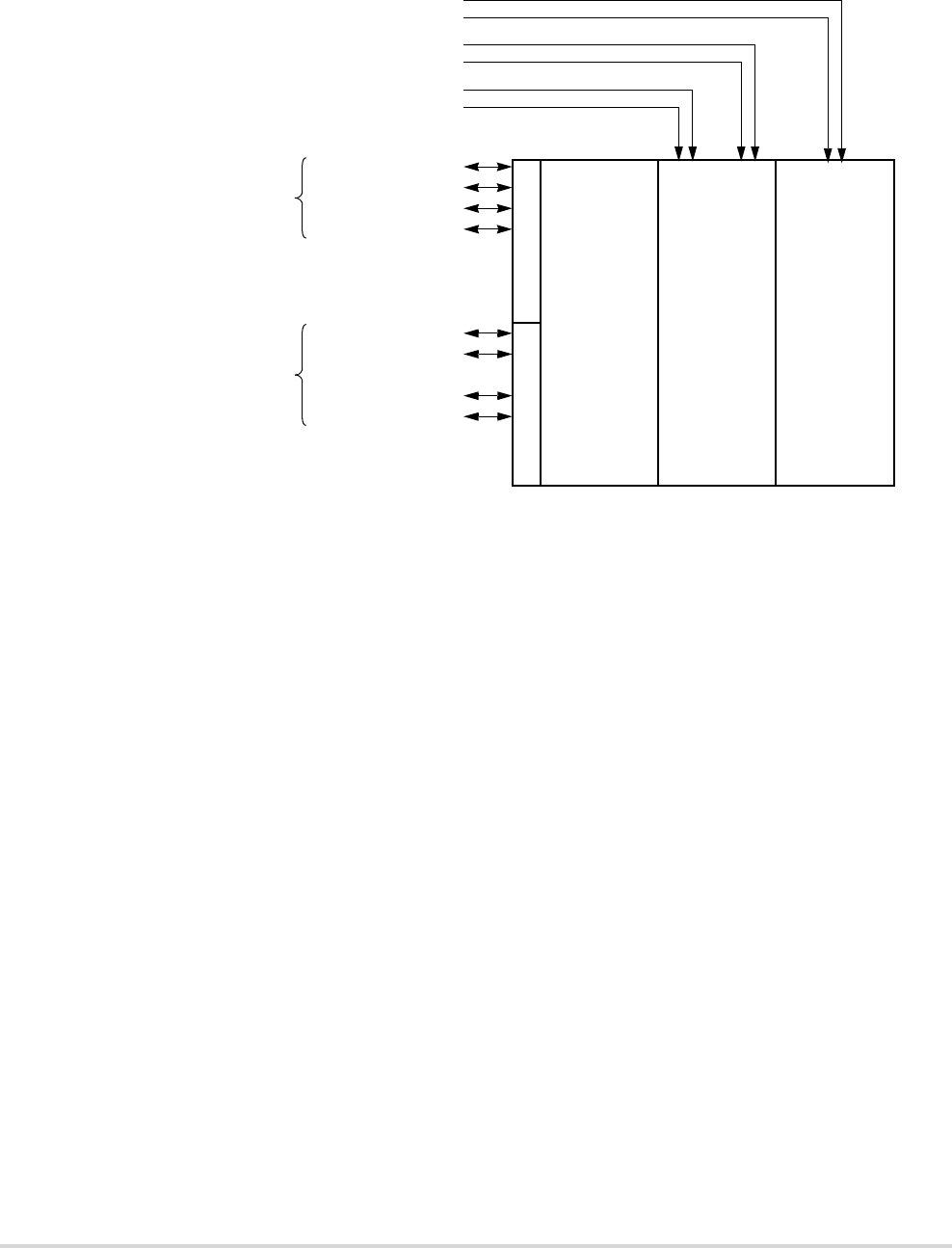
MOTOROLA Chapter 27. Queued Analog-to-Digital Converter (QADC) 27-5
Signals
Figure 27-2. QADC Input and Output Signals
27.4.1.2 Port QA Digital Input/Output Signals
Port QA signals are referred to as PQA[4:3, 1:0] when used as a bidirectional 4-bit digital
input/output port. These four signals may be used for general-purpose digital input or
digital output.
Port QA signals are connected to a digital input synchronizer during reads and may be used
as general-purpose digital inputs when the applied voltages meet high-voltage input (VIH)
and low-voltage input (VIL) requirements.
Each port QA signal is configured as an input or output by programming the port data
direction register (DDRQA). The digital input signal states are read from the port QA data
register (PORTQA) when DDRQA specifies that the signals are inputs. The digital data in
PORTQA is driven onto the port QA signals when the corresponding bits in DDRQA
specify output. See Section 27.6.4.
27.4.2 Port QB Signal Functions
The four port QB signals can be used as analog inputs or as a 4-bit digital I/O port.
27.4.2.1 Port QB Analog Input Signals
When used as analog inputs, the four port QB signals are referred to as AN[3:0].
AN52/MA0/PQA0
AN53/MA1/PQA1
AN55/ETRIG1/PQA3
AN56/ETRIG2/PQA4
AN0/ANW/PQB0
AN1/ANX/PQB1
AN2/ANY/PQB2
AN3/ANZ/PQB3
Digital
Analog
VSSI
Analog Power and Ground
Internal Digital Power
PORT QB
Converter
Results
and
Control
Analog
Mux and
Port QB Analog Inputs
External MUX Inputs
Digital Inputs
Port QA Analog Inputs
External Trigger Inputs
External MUX Address Outputs
VDDI
VSSA
VDDA
VRH
VRL
Analog References
Shared with Other Modules
Digital I/O
Port Logic
PORT QA

27-6 MCF5282 User’s Manual MOTOROLA
Signals
27.4.2.2 Port QB Digital I/O Signals
Port QB signals are referred to as PQB[3:0] when used as a 4-bit digital input/output port.
In addition to functioning as analog input signals, the port QB signals are also connected to
the input of a synchronizer during reads and may be used as general-purpose digital inputs
when the applied voltages meet VIH and VIL requirements.
Each port QB signal is configured as an input or output by programming the port data
direction register (DDRQB). The digital input signal states are read from the port QB data
register (PORTQB) when DDRQB specifies that the signals are inputs. The digital data in
PORTQB is driven onto the port QB signals when the corresponding bits in DDRQB
specify output. See Section 27.6.4.
27.4.3 External Trigger Input Signals
The QADC has two external trigger signals, ETRIG2 and ETRIG1. Each external trigger
input is associated with one of the scan queues, queue 1 or queue 2. The assignment of
ETRIG[2:1] to a queue is made by the TRG bit in QADC control register 0 (QACR0).
When TRG = 0, ETRIG1 triggers queue 1 and ETRIG2 triggers queue 2. When TRG = 1,
ETRIG1 triggers queue 2 and ETRIG2 triggers queue 1. See Section 27.6.5 “Control
Registers.”
27.4.4 Multiplexed Address Output Signals
In non-multiplexed mode, the QADC analog input signals are connected to an internal
multiplexer which routes the analog signals into the internal A/D converter.
In externally multiplexed mode, the QADC allows automatic channel selection through up
to four external 4-to-1 multiplexer chips. The QADC provides a 2-bit multiplexed address
output to the external multiplexer chips to allow selection of one of four inputs. The
multiplexed address output signals, MA1 and MA0, can be used as multiplexed address
output bits or as general-purpose I/O when external multiplexed mode is not being used.
MA[1:0] are used as the address inputs for up to four 4-channel multiplexer chips. Because
the MA[1:0] signals are digital outputs in multiplexed mode, the state of their
corresponding data direction bits in DDRQA is ignored.
27.4.5 Multiplexed Analog Input Signals
In external multiplexed mode, four of the port QB signals are redefined so that each
represent four analog input channels. See Table 27-1.

MOTOROLA Chapter 27. Queued Analog-to-Digital Converter (QADC) 27-7
Memory Map
27.4.6 Voltage Reference Signals
VRH and VRL are the dedicated input signals for the high and low reference voltages.
Separating the reference inputs from the power supply signals allows for additional external
filtering, which increases reference voltage precision and stability, and subsequently
contributes to a higher degree of conversion accuracy.
NOTE
VRH and VRL must be set to VDDA and VSSA potential,
respectively. For more information, refer to Section 27.9.
27.4.7 Dedicated Analog Supply Signals
The VDDA and VSSA signals supply power to the analog subsystems of the QADC module.
Dedicated power is required to isolate the sensitive analog circuitry from the normal levels
of noise present on the digital power supply.
27.4.8 Dedicated Digital I/O Port Supply Signal
VDDH provides 5-V power to the digital I/O functions of QADC port QA and port QB. This
allows those signals to tolerate 5 volts when configured as inputs and drive 5 volts when
configured as outputs.
27.5 Memory Map
The QADC occupies 1 Kbyte, or 512 half-word (16-bit) entries, of address space. Ten
half-word registers are control, port, and status registers, 64 half-word entries are the CCW
table, and 64 half-word entries are the result table which occupies 192 half-word address
locations because the result data is readable in three data alignment formats. Table 27-2 is
the QADC memory map.
Table 27-1. Multiplexed Analog Input Channels
Multiplexed
Analog Input Channels
ANW Even numbered channels from 0 to 6
ANX Odd numbered channels from 1 to 7
ANY Even numbered channels from 16 to 22
ANZ Odd numbered channels from 17 to 23

27-8 MCF5282 User’s Manual MOTOROLA
Register Descriptions
27.6 Register Descriptions
This subsection describes the QADC registers.
27.6.1 QADC Module Configuration Register (QADCMCR)
The QADCMCR contains bits that control QADC debug and stop modes and determine the
privilege level required to access most registers.
Table 27-2. QADC Memory Map
IPSBAR +
Offset MSB LSB Access 1
1S = CPU supervisor mode access only. S/U = CPU supervisor or user mode access. User mode accesses to supervisor only
addresses have no effect and result in a cycle termination transfer error.
0x19_0000 QADC Module Configuration Register (QADCMCR) S
0x19_0002 QADC Test Register (QADCTEST) 2
2Access results in the module generating an access termination transfer error if not in test mode.
S
0x19_0004 Reserved 3
3Read/writes have no effect and the access terminates with a transfer error exception.
—
0x19_0006 Port QA Data Register (PORTQA) Port QB Data Register (PORTQB) S/U
0x19_0008 Port QA Data Direction Register (DDRQA) Port QB Data Direction Register (DDRQB) S/U
0x19_000a QADC Control Register 0 (QACR0) S/U
0x19_000c QADC Control Register 1 (QACR1) S/U
0x19_000e QADC Control Register 2 (QACR2) S/U
0x19_0010 QADC Status Register 0 (QASR0) S/U
0x19_0012 QADC Status Register 1 (QASR1) S/U
0x19_0014–
0x19_01fe
Reserved(3) —
0x19_0200–
0x19_027e
Conversion Command Word Table (CCW) S/U
0x19_0280–
0x19_02fe
Right Justified, Unsigned Result Register (RJURR) S/U
0x19_0300–
0x19_037e
Left Justified, Signed Result Register (LJSRR) S/U
0x19_0380–
0x19_03fe
Left Justified, Unsigned Result Register (LJURR) S/U
15 14 13 8
Field QSTOP QDBG —
Reset 0000_0000
R/W: R/W R

MOTOROLA Chapter 27. Queued Analog-to-Digital Converter (QADC) 27-9
Register Descriptions
27.6.2 QADC Test Register (QADCTEST)
The QADCTEST is a reserved register. Attempts to access this register outside of factory
test mode will result in access privilege violation.
27.6.3 Port Data Registers (PORTQA and PORTQB)
QADC ports QA and QB are accessed through the 8-bit PORTQA and PORTQB.
Port QA signals are referred to as PQA[4:3, 1:0] when used as a bidirectional, 4-bit,
input/output port. Port QA can also be used for analog inputs (AN[56:55, 53:52]), external
trigger inputs (ETRIG[2:1]), and external multiplexer address outputs (MA[1:0]).
Port QB signals are referred to as PQB[3:0] when used as a 4-bit, digital input-only port.
Port QB can also be used for non-multiplexed (AN[3:0]) and multiplexed (ANZ, ANY,
ANX, ANW) analog inputs.
PORTQA and PORTQB are not initialized by reset.
76 0
Field SUPV —
Reset 1000_0000
R/W: R/W R
Address IPSBAR + 0x19_0000, 0x19_0001
Figure 27-3. QADC Module Configuration Register (QADCMCR)
Table 27-3. QADCMCR Field Descriptions
Bit(s) Name Description
15 QSTOP Stop enable.
1 Force QADC to idle state.
0 QADC operates normally.
14 QDBG Debug enable.
1 Finish any conversion in progress, then freeze in debug mode
0 QADC operates normally.
13–8 — Reserved, should be cleared.
7 SUPV Supervisor/unrestricted data space.
1 All QADC registers are accessible in supervisor mode only; user mode accesses have no
effect and result in a cycle termination error.
0 Only QADCMCR and QADCTEST require supervisor mode access; access to all other
QADC registers is unrestricted
6–0 — Reserved, should be cleared.

27-10 MCF5282 User’s Manual MOTOROLA
Register Descriptions
Note: The reset value for these fields is the current signal state if DDR is an input; otherwise, they are undefined.
27.6.4 Port QA and QB Data Direction Register
(DDRQA and DDRQB)
DDRQA and DDRQB are associated with port QA and QB digital I/O signals. Setting a bit
in these registers configures the corresponding signal as an output. Clearing a bit in these
registers configures the corresponding signal as an input. During QADC initialization, port
QA and QB signals that will be used as direct or multiplexed analog inputs must have their
corresponding data direction register bits cleared. When a port QA or QB signal that is
programmed as an output is selected for analog conversion, the voltage sampled is that of
the output digital driver as influenced by the load.
When the MUX (externally multiplexed) bit is set in QACR0, the data direction register
settings are ignored for the bits corresponding to PQA[1:0], and the two multiplexed
address (MA[1:0]) output signals. The MA[1:0] signals are forced to be digital outputs,
regardless of their data direction setting, and the multiplexed address outputs are driven.
The data returned during a port data register read is the value of the MA[1:0] signals,
regardless of their data direction setting.
Similarly, when the external trigger signals are assigned to port signals and external trigger
queue operating mode is selected, the data direction setting for the corresponding signals,
PQA3 and/or PQA4, is ignored. The port signals are forced to be digital inputs for ETRIG1
and/or ETRIG2. The data returned during a port data register read is the value of the
ETRIG[2:1] signals, regardless of their data direction setting.
76543210
Field — PQA4
(AN56)
(ETRIG2)
PQA3
(AN55)
(ETRIG1)
— PQA1
(AN53)
(MA1)
PQA0
(AN52)
(MA0)
Reset 000 See Note 0 See Note
R/W: R R/W R R/W
Address IPSBAR + 0x19_0006
Figure 27-4. QADC Port QA Data Register (PORTQA)
76543210
Field — PQB3
(AN3)
(ANZ)
PQB2
(AN2)
(ANY)
PQA1
(AN1)
(ANX)
PQA0
(AN0)
(ANW)
Reset 0000 See Note
R/W: R R/W
Address IPSBAR + 0x19_0007
Figure 27-5. QADC Port QB Data Register (PORTQB)

MOTOROLA Chapter 27. Queued Analog-to-Digital Converter (QADC) 27-11
Register Descriptions
NOTE
Use caution when mixing digital and analog inputs. They
should be isolated as much as possible. Rise and fall times
should be as large as possible to minimize ac coupling effects.
27.6.5 Control Registers
This subsection describes the QADC control registers.
27.6.5.1 QADC Control Register 0 (QACR0)
QACR0 establishes the QADC sampling clock (QCLK) with prescaler parameter fields and
defines whether external multiplexing is enabled. Typically, these bits are written once
when the QADC is initialized and not changed thereafter. The bits in this register are read
anytime, write anytime (except during stop mode).
76543210
Field — DDQA4 DDQA3 — DDQA1 DDQA0
Reset 0000_0000
R/W: R R/W R R/W
Address IPSBAR + 0x19_0008
Figure 27-6. QADC Port QA Data Direction Register (DDRQA)
76543210
Field — DDQB3 DDQB2 DDQB1 DDQB0
Reset 0000_0000
R/W R
Address IPSBAR + 0x19_0009
Figure 27-7. Port QB Data Direction Register (DDRQB)

27-12 MCF5282 User’s Manual MOTOROLA
Register Descriptions
15 14 13 12 11 8
Field MUX — TRG —
Reset 0000_0000
R/W: R/W R R/W R
7 6 5 4 3210
Field — QPR6 QPR5 QPR4 QPR3 QPR2 QPR1 QPR0
Reset 0001_0011
R/W: R R/W
Address IPSBAR + 0x19_000a, 0x19_000b
Figure 27-8. QADC Control Register 0 (QACR0)
Table 27-4. QACR0 Field Descriptions
Bit(s) Name Description
15 MUX Externally multiplexed mode. Configures the QADC for operation in externally multiplexed
mode, which affects the interpretation of the channel numbers and forces the MA[1:0] signals
to be outputs.
1 Externally multiplexed, up to 18 possible channels
0 Internally multiplexed, up to 8 possible channels
14–13 — Reserved, should be cleared.
12 TRG Trigger assignment. Determines the queue assignment of the ETRIG[2:1] signals.
1 ETRIG1 triggers queue 2; ETRIG2 triggers queue 1.
0 ETRIG1 triggers queue 1; ETRIG2 triggers queue 2.
11–7 — Reserved, should be cleared.
6–0 QPR Prescaler clock divider. Selects the system clock divisor to generate the QADC clock as
Table 27-5 shows. The resulting QADC clock rate can be given as:
where:
1 ≤ QPR[6:0] ≤ 127.
If QPR[6:0] = 0, then the QPR register field value is read as a 1 and the prescaler divisor is 2.
The prescaler should be selected so that the QADC clock rate is within the required fQCLK
range. See MCF5282 Electrical Characteristics.
fQCLK =
fSYS
2(QPR[6:0] + 1)

MOTOROLA Chapter 27. Queued Analog-to-Digital Converter (QADC) 27-13
Register Descriptions
Table 27-5. Prescaler fSYS Divide-by Values
QPR[6:0] fSYS
Divisor QPR[6:0] fSYS
Divisor QPR[6:0] fSYS
Divisor QPR[6:0] fSYS
Divisor
0000000 4 0100000 66 1000000 130 1100000 194
0000001 4 0100001 68 1000001 132 1100001 196
0000010 6 0100010 70 1000010 134 1100010 198
0000011 8 0100011 72 1000011 136 1100011 200
0000100 10 0100100 74 1000100 138 1100100 202
0000101 12 0100101 76 1000101 140 1100101 204
0000110 14 0100110 78 1000110 142 1100110 206
0000111 16 0100111 80 1000111 144 1100111 208
0001000 18 0101000 82 1001000 146 1101000 210
0001001 20 0101001 84 1001001 148 1101001 212
0001010 22 0101010 86 1001010 150 1101010 214
0001011 24 0101011 88 1001011 152 1101011 216
0001100 26 0101100 90 1001100 154 1101100 218
0001101 28 0101101 92 1001101 156 1101101 220
0001110 30 0101110 94 1001110 158 1101110 222
0001111 32 0101111 96 1001111 160 1101111 224
0010000 34 0110000 98 1010000 162 1110000 226
0010001 36 0110001 100 1010001 164 1110001 228
0010010 38 0110010 102 1010010 166 1110010 230
0010011 40 0110011 104 1010011 168 1110011 232
0010100 42 0110100 106 1010100 170 1110100 234
0010101 44 0110101 108 1010101 172 1110101 236
0010110 46 0110110 110 1010110 174 1110110 238
0010111 48 0110111 112 1010111 176 1110111 240
0011000 50 0111000 114 1011000 178 1111000 242
0011001 52 0111001 116 1011001 180 1111001 244
0011010 54 0111010 118 1011010 182 1111010 246
0011011 56 0111011 120 1011011 184 1111011 248
0011100 58 0111100 122 1011100 186 1111100 250
0011101 60 0111101 124 1011101 188 1111101 252
0011110 62 0111110 126 1011110 190 1111110 254
0011111 64 0111111 128 1011111 192 1111111 256

27-14 MCF5282 User’s Manual MOTOROLA
Register Descriptions
27.6.5.2 QADC Control Register 1 (QACR1)
QACR1 is the mode control register for queue 1. This register governs queue operating
mode and the use of completion and/or pause interrupts. Typically, these bits are written
once when the QADC is initialized and are not changed thereafter.
Stop mode resets this register.
15 14 13 12 11 10 9 8
Field CIE1 PIE1 SSE1 MQ112 MQ111 MQ110 MQ19 MQ18
Reset 0000_0000
R/W: R/W
7 0
Field —
Reset 0000_0000
R/W: R
Address IPSBAR + 0x19_000c, 0x19_000d
Figure 27-9. QADC Control Register 1 (QACR1)
Table 27-6. QACR1 Field Descriptions
Bit(s) Name Description
15 CIE1 Queue 1 completion interrupt enable. Enables an interrupt request upon completion of queue 1.
The interrupt request is initiated when the conversion is complete for the last CCW in queue 1.
1 Enable queue 1 completion interrupt.
0 Disable queue 1 completion interrupt.
14 PIE1 Queue 1 pause interrupt enable. Enables an interrupt request when queue 1 enters the pause
state. The interrupt request is initiated when conversion is complete for a CCW that has the
pause bit set.
1 Enable the queue 1 pause interrupt.
0 Disable the queue 1 pause interrupt.
13 SSE1 Queue 1 single-scan enable. Enables a single-scan of queue 1 after a trigger event occurs. SSE1
may be set during the same write cycle that sets the MQ1 bits for one of the single-scan queue
operating modes. The single-scan enable bit can be written to 1 or 0, but is always read as a 0,
unless the QADC is in test mode. The QADC clears SSE1 when the single-scan is complete.
1 Allow a trigger event to start queue 1 in a single-scan mode.
0 Trigger events are ignored for queue 1 single-scan modes.
12–8 MQ1nSelects the operating mode for queue 1. Table 27-7 shows the bits in the MQ1 field which
enable different queue 1 operating modes.
7–0 — Reserved, should be cleared.

MOTOROLA Chapter 27. Queued Analog-to-Digital Converter (QADC) 27-15
Register Descriptions
Table 27-7. Queue 1 Operating Modes
MQ1[12:8] Operating Mode
00000 Disabled mode, conversions do not occur
00001 Software-triggered single-scan mode (started with SSE1)
00010 External-trigger rising-edge single-scan mode
00011 External-trigger falling-edge single-scan mode
00100 Interval timer single-scan mode: time = QCLK period × 27
00101 Interval timer single-scan mode: time = QCLK period × 28
00110 Interval timer single-scan mode: time = QCLK period × 29
00111 Interval timer single-scan mode: time = QCLK period × 210
01000 Interval timer single-scan mode: time = QCLK period × 211
01001 Interval timer single-scan mode: time = QCLK period × 212
01010 Interval timer single-scan mode: time = QCLK period × 213
01011 Interval timer single-scan mode: time = QCLK period × 214
01100 Interval timer single-scan mode: time = QCLK period × 215
01101 Interval timer single-scan mode: time = QCLK period × 216
01110 Interval timer single-scan mode: time = QCLK period × 217
01111 Externally gated single-scan mode (started with SSE1)
10000 Reserved mode
10001 Software-triggered continuous-scan mode
10010 External-trigger rising-edge continuous-scan mode
10011 External-trigger falling-edge continuous-scan mode
10100 Periodic timer continuous-scan mode: time = QCLK period × 27
10101 Periodic timer continuous-scan mode: time = QCLK period × 28
10110 Periodic timer continuous-scan mode: time = QCLK period × 29
10111 Periodic timer continuous-scan mode: time = QCLK period × 210
11000 Periodic timer continuous-scan mode: time = QCLK period × 211
11001 Periodic timer continuous-scan mode: time = QCLK period × 212
11010 Periodic timer continuous-scan mode: time = QCLK period × 213
11011 Periodic timer continuous-scan mode: time = QCLK period × 214
11100 Periodic timer continuous-scan mode: time = QCLK period × 215
11101 Periodic timer continuous-scan mode: time = QCLK period × 216
11110 Periodic timer continuous-scan mode: time = QCLK period × 217
11111 Externally gated continuous-scan mode

27-16 MCF5282 User’s Manual MOTOROLA
Register Descriptions
27.6.5.3 QADC Control Register 2 (QACR2)
QACR2 is the mode control register for queue 2. This register governs queue operating
mode and the use of completion and/or pause interrupts. Typically, these bits are written
once when the QADC is initialized and not changed thereafter.
QACR2 also includes a resume feature that selects the resumption point for queue 2 after
its operation is suspended by a queue 1 trigger event. The primary reason for selecting
re-execution of the entire queue or subqueue is to guarantee that all samples are taken
consecutively in one scan (coherency).
When subqueues are not used, queue 2 execution restarts after suspension with the first
CCW in queue 2. When a pause has previously occurred in queue 2 execution, queue
execution restarts after suspension with the first CCW in the current subqueue.
A subqueue is considered to be a stand-alone sequence of conversions. Once a pause flag
has been set to report subqueue completion, that subqueue is not repeated until all CCWs
in queue 2 are executed.
For example, the RESUME bit can be used when the frequency of queue 1 trigger events
prohibit queue 2 completion. If the rate of queue 1 execution is too high, it is best for queue
2 execution to continue with the CCW that was being converted when queue 2 was
suspended. This allows queue 2 to eventually complete execution.
The beginning of queue 2 is defined by programming the BQ2 field in QACR2. BQ2 is
usually set before or at the same time as the queue operating mode for queue 2 is selected.
If BQ2[6:0] ≥ 64, queue 2 has no entries, the entire CCW table is dedicated to queue 1, and
CCW63 is the end-of-queue 1. If BQ2[6:0] is 0, the entire CCW table is dedicated to queue
2. A special case occurs when an operating mode is selected for queue 1 and a trigger event
occurs for queue 1 with BQ2 set to 0. Queue 1 execution starts momentarily, but is
terminated after CCW0 is read. No conversions occur.
The BQ2[6:0] pointer may be changed dynamically to alternate between queue 2 scan
sequences. A change in BQ2 after queue 2 has begun or when queue 2 has a trigger pending
does not affect queue 2 until it is started again. For example, two scan sequences could be
defined as follows: The first sequence starts at CCW10, with a pause after CCW11 and an
end of queue (EOQ) programmed in CCW15; the second sequence starts at CCW16, with
a pause after CCW17 and an EOQ programmed in CCW39.
With BQ2[6:0] set to CCW10 and the continuous-scan mode selected, queue execution
begins. When the pause is encountered in CCW11, an interrupt service routine can retarget
BQ2[6:0] to CCW16. When the end-of-queue is recognized in CCW15, an internal
retrigger event is generated and execution restarts at CCW16. When the pause software
interrupt occurs again, BQ2 can be changed back to CCW10. After the end-of-queue is
recognized in CCW39, an internal retrigger event is created and execution now restarts at
CCW10.

MOTOROLA Chapter 27. Queued Analog-to-Digital Converter (QADC) 27-17
Register Descriptions
If BQ2[6:0] is changed while queue 1 is active, the effect of BQ2[6:0] as an end-of-queue
indication for queue 1 is immediate. However, beware of the risk of losing the end-of-queue
1 when changing BQ2[6:0]. Using EOQ (channel 63) to end queue 1 is recommended.
NOTE
If BQ2[6:0] was assigned to the CCW that queue 1 is currently
working on, then that conversion is completed before the
change to BQ2[6:0] takes effect.
Each time a CCW is read for queue 1, the CCW location is compared with the current value
of the BQ2[6:0] pointer to detect a possible end-of-queue condition. For example, if
BQ2[6:0] is changed to CCW3 while queue 1 is converting CCW2, queue 1 is terminated
after the conversion is completed. However, if BQ2[6:0] is changed to CCW1 while queue
1 is converting CCW2, the QADC would not recognize a BQ2[6:0] end-of-queue condition
until queue 1 execution reached CCW1 again, presumably on the next pass through the
queue.
Stop mode resets this register (0x007f)
15 14 13 12 11 10 9 8
Field CIE2 PIE2 SSE2 MQ212 MQ211 MQ210 MQ29 MQ28
Reset 0000_0000
R/W: R/W
7 6 5 4 3210
Field RESUME BQ26 BQ25 BQ24 BQ23 BQ22 BQ21 BQ20
Reset 0111_1111
R/W: R/W
Address IPSBAR + 0x19_000e, 0x19_000f
Figure 27-10. QADC Control Register 2 (QACR2)

27-18 MCF5282 User’s Manual MOTOROLA
Register Descriptions
Table 27-8. QACR2 Field Descriptions
Bit(s) Name Description
15 CIE2 Queue 2 completion software interrupt enable. Enables an interrupt request upon completion of
queue 2. The interrupt request is initiated when the conversion is complete for the last CCW in
queue 2.
1 Enable queue 2 completion interrupt.
0 Disable queue 2 completion interrupt.
14 PIE2 Queue 2 pause interrupt enable. Enables an interrupt request when queue 2 enters the pause
state. The interrupt request is initiated when conversion is complete for a CCW that has the
pause bit set.
1 Enable the queue 2 pause interrupt.
0 Disable the queue 2 pause interrupt.
13 SSE2 Queue 2 single-scan enable. Enables a single-scan of queue 2 after a trigger event occurs. SSE2
may be set during the same write cycle that sets the MQ2 bits for one of the single-scan queue
operating modes. The single-scan enable bit can be written to 1 or 0, but is always read as a 0,
unless the QADC is in test mode. The QADC clears SSE2 when the single-scan is complete.
1 Allow a trigger event to start queue 2 in a single-scan mode.
0 Trigger events are ignored for queue 2 single-scan modes.
12–8 MQ2 Selects the operating mode for queue 2. Table 27-9 shows the bits in the MQ1 field which
enable different queue 2 operating modes.
7 RESUME Selects the resumption point for queue 2 after its operation is suspended due to a queue 1 trigger
event. If RESUME is changed during the execution of queue 2, the change is not recognized
until an end-of-queue condition is reached or the operating mode of queue 2 is changed.
1 After suspension, begin execution with the aborted CCW in queue 2.
0 After suspension, begin execution with the first CCW of queue 2 or the current subqueue of
queue 2.
6–0 BQ2 Beginning of queue 2. Denotes the CCW location where queue 2 begins. This allows the length
of queue 1 and queue 2 to vary. The BQ2 field also serves as an end-of-queue condition for
queue 1.
Table 27-9. Queue 2 Operating Modes
MQ2[12:8] Operating Modes
00000 Disabled mode, conversions do not occur
00001 Software triggered single-scan mode (started with SSE2)
00010 Externally triggered rising edge single-scan mode
00011 Externally triggered falling edge single-scan mode
00100 Interval timer single-scan mode: time = QCLK period x 27
00101 Interval timer single-scan mode: time = QCLK period x 28
00110 Interval timer single-scan mode: time = QCLK period x 29
00111 Interval timer single-scan mode: time = QCLK period x 210
01000 Interval timer single-scan mode: time = QCLK period x 211
01001 Interval timer single-scan mode: time = QCLK period x 212
01010 Interval timer single-scan mode: time = QCLK period x 213

MOTOROLA Chapter 27. Queued Analog-to-Digital Converter (QADC) 27-19
Register Descriptions
27.6.6 Status Registers
This subsection describes the QADC status registers.
27.6.6.1 QADC Status Register 0 (QASR0)
QASR0 contains information about the state of each queue and the current A/D conversion.
The bits in this register are read anytime. For flag bits (CF1, PF1, CF2, PF2, TOR1, TOR2),
writing a 1 has no effect; writing a 0 clears the bit. For QS[9:6] and CWP, writes have no
effect. Stop mode resets this register.
The end of a queue is identified in the following cases:
• When execution is complete on the CCW in the location prior to the one
pointed to by BQ2
01011 Interval timer single-scan mode: time = QCLK period x 214
01100 Interval timer single-scan mode: time = QCLK period x 215
01101 Interval timer single-scan mode: time = QCLK period x 216
01110 Interval timer single-scan mode: time = QCLK period x 217
01111 Reserved mode
10000 Reserved mode
10001 Software triggered continuous-scan mode
10010 Externally triggered rising edge continuous-scan mode
10011 Externally triggered falling edge continuous-scan mode
10100 Periodic timer continuous-scan mode: time = QCLK period x 27
10101 Periodic timer continuous-scan mode: time = QCLK period x 28
10110 Periodic timer continuous-scan mode: time = QCLK period x 29
10111 Periodic timer continuous-scan mode: time = QCLK period x 210
11000 Periodic timer continuous-scan mode: time = QCLK period x 211
11001 Periodic timer continuous-scan mode: time = QCLK period x 212
11010 Periodic timer continuous-scan mode: time = QCLK period x 213
11011 Periodic timer continuous-scan mode: time = QCLK period x 214
11100 Periodic timer continuous-scan mode: time = QCLK period x 215
11101 Periodic timer continuous-scan mode: time = QCLK period x 216
11110 Periodic timer continuous-scan mode: time = QCLK period x 217
11111 Reserved mode
Table 27-9. Queue 2 Operating Modes (continued)
MQ2[12:8] Operating Modes

27-20 MCF5282 User’s Manual MOTOROLA
Register Descriptions
• When the current CCW contains the end-of-queue code (channel 63) instead of a
valid channel number
• When the currently completed CCW is in the last location of the CCW RAM.
Once PFn is set, the queue enters the paused state and waits for a trigger event to allow
queue execution to continue. However, a special case occurs when the CCW with the pause
bit set is the last CCW in a queue; queue execution is complete. The queue status becomes
idle, not paused, and both the pause and completion flags are set.
Another special case occurs when the queue is operating in software-initiated single-scan
or continuous-scan mode and a CCW pause bit is set. The QADC will set PFn and will also
automatically generate a retrigger event that restarts execution after two QCLK cycles.
Pause mode is never entered.
In externally gated single-scan and continuous-scan mode, the behavior of PFn has been
redefined. When the gate closes before the end of the queue is reached, PFn is set to indicate
that an incomplete scan has occurred. In single-scan mode, a resultant interrupt can be used
to determine if the queue should be enabled again. In either externally gated mode, setting
PFn indicates that the results for the queue have not been collected during one scan
(coherently).
NOTE:
If a set CCW pause bit is encountered in either externally gated
mode, the pause flag will not set, and execution continues
without pausing. This has allowed for the modified behavior of
PF1 in the externally gated modes.
PFn is maintained by the QADC regardless of whether the
corresponding interrupt is enabled. PFn may be polled to
determine if the QADC has reached a pause in scanning a
queue.
A trigger event generated by a transition on the external trigger signal or by the
periodic/interval timer may be captured as a trigger overrun. TORn cannot be set when the
software-initiated single-scan mode or the software-initiated continuous-scan mode is
selected.
TORn is set when a trigger event is received while a queue is executing and before the scan
has completed or paused. TORn has no effect on queue execution.
After a trigger event has occurred for queue 1, and before the scan has completed or paused,
additional queue 1 trigger events are not retained. Such trigger events are considered
unexpected, and the QADC sets the TORn error status bit. An unexpected trigger event may
denote a system overrun situation.
In externally gated continuous-scan mode, the behavior of TORn has been redefined. In the
case that the queue reaches an end-of-queue condition for the second time during an open

MOTOROLA Chapter 27. Queued Analog-to-Digital Converter (QADC) 27-21
Register Descriptions
gate, TORn is set. This is considered an overrun condition. In this case, CF1 has been set
for the first end-of-queue condition and TORn sets for the second end-of-queue condition.
For TOR1 to set, CF2 must not be cleared before the second end-of-queue.
The QS field indicates the status of queue 1 and queue 2. Following are the five queue status
conditions:
• Idle
•Active
•Paused
• Suspended
• Trigger pending
The idle state occurs when a queue is disabled, when a queue is in a reserved mode, or when
a queue is in a valid queue operating mode awaiting a trigger event to initiate queue
execution. One or both queues may be in the idle state. When a queue is idle, CCWs are not
being executed for that queue, the queue is not in the pause state, and no trigger is pending.
A queue is in the active state when a valid queue operating mode is selected, when the
selected trigger event has occurred, or when the QADC is performing a conversion
specified by a CCW from that queue. Only one queue can be active at a time.
One or both queues can be in the paused state. A queue is paused when the previous CCW
executed from that queue had the pause bit set. The QADC does not execute any CCWs
from the paused queue until a trigger event occurs. Consequently, the QADC can service
queue 2 while queue 1 is paused.
Only queue 2 can be in the suspended state. When a trigger event occurs on queue 1 while
queue 2 is executing, the current queue 2 conversion is aborted and the queue 2 status is
reported as suspended. Queue 2 transitions back to the active state when queue 1 becomes
idle or paused.
A trigger pending state is required because both queues cannot be active at the same time.
The status of queue 2 is changed to trigger pending when a trigger event occurs for queue
2 while queue 1 is active. In the opposite case, when a trigger event occurs for queue 1 while
queue 2 is active, queue 2 is aborted and the status is reported as queue 1 active, queue 2
suspended. So due to the priority scheme, only queue 2 can be in the trigger pending state.
Two transition cases cause the queue 2 status to be trigger pending before queue 2 is shown
to be in the active state. When queue 1 is active and there is a trigger pending on queue 2,
after queue 1 completes or pauses, queue 2 continues to be in the trigger pending state for
a few clock cycles. The fleeting status conditions are:
• Queue 1 idle with queue 2 trigger pending
• Queue 1 paused with queue 2 trigger pending
Figure 27-12 displays the status conditions of the QS field as the QADC goes through the
transition from queue 1 active to queue 2 active.

27-22 MCF5282 User’s Manual MOTOROLA
Register Descriptions
When a queue enters the paused state, CWP points to the CCW with the pause bit set. While
in pause, the CWP value is maintained until a trigger event occurs on either queue. Usually,
the CWP is updated a few clock cycles before the queue status field shows that the queue
has become active. For example, a read of CWP may point to a CCW in queue 2, while the
queue status field shows queue 1 paused and queue 2 trigger pending.
When the QADC finishes a queue scan, the CWP points to the CCW where the
end-of-queue condition was detected. Therefore, when the end-of-queue condition is a
CCW with the EOQ code (channel 63), the CWP points to the CCW containing the EOQ.
When the last CCW in a queue is the last CCW table location (CCW63), and it does not
contain the EOQ code, the end-of-queue is detected when the following CCW is read, so
the CWP points to word CCW0.
Finally, when queue 1 operation is terminated after a CCW is read that is pointed to by BQ2,
the CWP points to the same CCW as BQ2.
15 14 13 12 11 10 9 8
Field CF1 PF1 CF2 PF2 TOR1 TOR2 QS9 QS8
Reset 0000_0000
R/W: R/W R
7 6 5 4 3210
Field QS7 QS6 CWP5 CWP4 CWP3 CWP2 CWP1 CWP0
Reset 0000_0000
R/W: R
Address IPSBAR + 0x19_0010, 0x19_0011
Figure 27-11. QADC Status Register 0 (QASR0)

MOTOROLA Chapter 27. Queued Analog-to-Digital Converter (QADC) 27-23
Register Descriptions
Table 27-10. QASR0 Field Descriptions
Bit(s) Name Description
15, 13 CFnQueue completion flag. Indicates that a queue scan has been completed. CF[1:2] is set by the
QADC when the input channel sample requested by the last CCW in the queue is converted,
and the result is stored in the result table.
When CFn is set and queue completion interrupts are enabled (QACRn[CIEn] = 1), the QADC
requests an interrupt. The interrupt request is cleared when a 0 is written to the CF1 bit after it
has been read as a 1. Once set, CF1 can be cleared only by a reset or by writing a 0 to it.
CF[1:2] is updated by the QADC regardless of whether the corresponding interrupt is enabled.
This allows polled recognition of the queue scan completion.
14, 12 PFnQueue pause flag. Indicates that a queue scan has reached a pause. PF[1:2] is set by the QADC
when the current queue 1 CCW has the pause bit set, the selected input channel has been
converted, and the result has been stored in the result table.
When PFn is set and interrupts are enabled (QACRn[PIEn] = 1), the QADC requests an
interrupt. The interrupt request is cleared when a 0 is written to PFn, after it has been read as a
1. Once set, PFn can be cleared only by reset or by writing a 0 to it.
PF1:
1 Queue 1 has reached a pause or gate closed before end-of-queue in gated mode.
0 Queue 1 has not reached a pause or gate has not closed before end-of-queue in gated mode.
PF2:
1 Queue 2 has reached a pause.
0 Queue 2 has not reached a pause.
See Table 27-11 for a summary of CCW pause bit response in all scan modes.
11–10 TORnQueue trigger overrun flag. Indicates that an unexpected trigger event has occurred for queue
1. TOR[1:2] can be set only while the queue is in the active state.
Once set, TOR[1:2] is cleared only by a reset or by writing a 0 to it.
1 At least one unexpected queue 1 trigger event has occurred or queue 1 reaches an
end-of-queue condition for the second time in externally gated continuous scan.
0 No unexpected queue 1 trigger events have occurred.
9–6 QS Queue status. Indicates the current condition of queue 1 and queue 2. The two most significant
bits are associated primarily with queue 1, and the remaining two bits are associated with queue
2. Because the priority scheme between the two queues causes the status to be interlinked, the
status bits must be considered as one 4-bit field. Table 27-12 shows the bits in the QS field and
how they denote the status of queue 1 and queue 2.
The queue status field is affected by QADC stop mode. Because all of the analog logic and
control registers are reset, the queue status field is reset to queue 1 idle, queue 2 idle.
During debug mode, the queue status field is not modified. The queue status field retains the
status it held prior to freezing. As a result, the queue status can show queue 1 active, queue 2
idle, even though neither queue is being executed during freeze.
5–0 CWP Command word pointer. Denotes which CCW is executing at present or was last completed.
CWP is a read-only field with a valid range of 0 to 63; write operations have no effect.
During stop mode, CWP is reset to 0 because the control registers and the analog logic are reset.
When debug mode is entered, CWP is not changed; it points to the last executed CCW.
Table 27-11. CCW Pause Bit Response
Scan Mode Queue Operation PF Asserts?
Externally triggered single-scan Pauses Yes
Externally triggered continuous-scan Pauses Yes
Interval timer trigger single-scan Pauses Yes

27-24 MCF5282 User’s Manual MOTOROLA
Register Descriptions
Interval timer continuous-scan Pauses Yes
Software-initiated single-scan Continues Yes
Software-initiated continuous-scan Continues Yes
Externally gated single-scan Continues No
Externally gated continuous-scan Continues No
Table 27-12. Queue Status
QS[9:6] Queue 1/Queue 2 States
0000 Queue 1 idle, queue 2 idle
0001 Queue 1 idle, queue 2 paused
0010 Queue 1 idle, queue 2 active
0011 Queue 1 idle, queue 2 trigger pending
0100 Queue 1 paused, queue 2 idle
0101 Queue 1 paused, queue 2 paused
0110 Queue 1 paused, queue 2 active
0111 Queue 1 paused, queue 2 trigger pending
1000 Queue 1 active, queue 2 idle
1001 Queue 1 active, queue 2 paused
1010 Queue 1 active, queue 2 suspended
1011 Queue 1 active, queue 2 trigger pending
1100 Reserved
1101 Reserved
1110 Reserved
1111 Reserved
Table 27-11. CCW Pause Bit Response (continued)
Scan Mode Queue Operation PF Asserts?
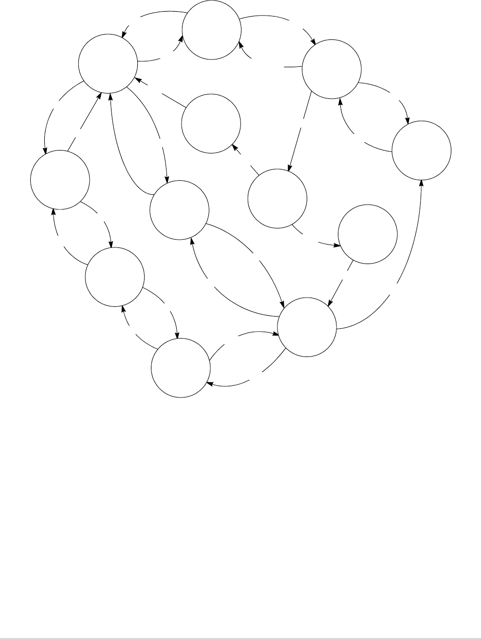
MOTOROLA Chapter 27. Queued Analog-to-Digital Converter (QADC) 27-25
Register Descriptions
Figure 27-12. Queue Status Transition
Q1 Idle/
Q2 Active
Q1 Idle/
Q2 Idle
Q1 Active/
Q2 Idle
Q1 Paused/
Q2 Idle
Q1 Active/
Q2 Suspended
Q1 Active/
Q2 Paused
Q1 Paused/
Q2 Active
Q1 Idle/
Q2 Paused
Q1 Paused/
Q2 Paused
Q1 Active/
Q2 Trigger
Pending
Q1 Paused/
Q2 Trigger
Pending
(Temporary)
Q2 Complete
Delayed Transition
Q1 Pause Bit Set
Q2 Trigger Event
Q1 Trigger Event
Q1 Pause Bit Set
Q1 Complete
Q1 Trigger Event
Q1 Complete
Delayed Transition
Q1 Complete
Q1 Pause Bit Set
Q1 Trigger Event
Q2 Complete
Q2 Pause Bit Set
Q2 Trigger Event
Q1 Trigger Event
Q1 Complete
Q1 Trigger Event
Q1 Pause Bit Set
Q2 Pause Bit Set
Q2 Trigger Event
Q1 Idle/
Q2 Trigger
Pending
(Temporary)
Q1 Trigger Event
Q2 Trigger Event

27-26 MCF5282 User’s Manual MOTOROLA
Register Descriptions
27.6.6.2 QADC Status Register 1 (QASR1)
Stop mode resets this register .
27.6.7 Conversion Command Word Table (CCW)
The CCW table is 64 half-word (128 byte) long RAM with 10 bits of each entry
implemented. The CCW table is written by the user and is not modified by the QADC. Each
CCW requests the conversion of one analog channel to a digital result. The CCW specifies
the analog channel number, the input sample time, and whether the queue is to pause after
15 14 13 12 11 10 9 8
Field — CWPQ15 CWPQ14 CWPQ13 CWPQ12 CWPQ11 CWPQ10
Reset 0011_1111
R/W: R
7 6 5 4 3210
Field — CWPQ25 CWPQ24 CWPQ23 CWPQ22 CWPQ21 CWPQ20
Reset 0011_1111
R/W: R
Address IPSBAR + 0x19_0012, 0x19_0013
Figure 27-13. QADC Status Register 1 (QASR1)
Table 27-13. QASR1 Field Descriptions
Bit(s) Name Description
15–14 — Reserved, should be cleared.
13–8 CWPQ1 Queue 1 command word pointer. Points to the last queue 1 CCW executed. This is a read-only
field with a valid range of 0 to 63; writes have no effect. CWPQ1 always points to the last
executed CCW in queue 1, regardless of which queue is active.
In contrast to CWP, CPWQ1 is updated when a conversion result is written. When the QADC
finishes a conversion in queue 1, both the result register is written and CWPQ1 is updated.
When queue 1 operation is terminated after a CCW is read that is pointed to by BQ2, CWP
points to BQ2 while CWPQ1 points to the last queue 1 CCW.
During stop mode, CWPQ1 is reset to 63, because the control registers and the analog logic are
reset. When debug mode is entered, CWPQ1 is not changed; it points to the last executed CCW
in queue 1.
7–6 — Reserved, should be cleared.
5–0 CWPQ Queue 2 command word pointer. Points to the last queue 2 CCW executed. This is a read-only
field with a valid range of 0 to 63; writes have no effect. CWPQ2 always points to the last
executed CCW in queue 2, regardless which queue is active.
In contrast to CWP, CPWQ2 is updated when a conversion result is written. When the QADC
finishes a conversion in queue 2, both the result register is written and CWPQ2 is updated.
During stop mode, CWPQ2 is reset to 63 because the control registers and the analog logic are
reset. When debug mode is entered, CWPQ2 is not changed; it points to the last executed CCW
in queue 2.

MOTOROLA Chapter 27. Queued Analog-to-Digital Converter (QADC) 27-27
Register Descriptions
the current CCW. The bits in this register are read anytime (except during stop mode), write
anytime (except during stop mode).
15 10 9 8
Field — P BYP
Reset 0000_00 Unaffected
R/W: R R/W
7 6 5 4 3210
Field IST1 IST0 CHAN5 CHAN4 CHAN3 CHAN2 CHAN1 CHAN0
Reset Undefined
R/W: R
Address IPSBAR + 0x19_0200, 0x19_027e
Figure 27-14. Conversion Command Word Table (CCW)
Table 27-14. CCW Field Descriptions
Bit(s) Name Description
15–10 — Reserved, should be cleared.
9 P Pause. Allows subqueues to be created within queue 1 and queue 2. The QADC performs the
conversion specified by the CCW with the pause bit set and then the queue enters the pause
state. Another trigger event causes execution to continue from the pause to the next CCW.
1 Enter pause state after execution of current CCW.
0 Do not enter pause state after execution of current CCW.
NOTE: The P bit does not cause the queue to pause in software-initiated modes or externally
gated modes.
8 BYP Sample amplifier bypass. Enables the amplifier bypass mode for a conversion and subsequently
changes the timing. The initial sample time is eliminated, reducing the potential conversion
time by two QCLKs. However, due to internal RC effects, a minimum final sample time of four
QCLKs must be allowed. When using this mode, the external circuit should be of low source
impedance. Loading effects of the external circuitry need to be considered because the benefits
of the sample amplifier are not present.
1 Amplifier bypass mode enabled
0 Amplifier bypass mode disabled
NOTE: BYP is maintained for software compatibility but has no functional benefit on this
version of the QADC.

27-28 MCF5282 User’s Manual MOTOROLA
Register Descriptions
7–6 IST Input sample time. Specifies the length of the sample window. The input sample time can be
varied, under software control, to accommodate various input channel source impedances.
Longer sample times permit more accurate A/D conversions of signals with higher source
impedances.
Table 27-15 shows the four selectable input sample times.
The programmable sample time can also be used to adjust queue execution time or sampling
rate by increasing the time interval between conversions.
5–0 CHAN Selects the input channel number. The CCW channel field is programmed with the channel
number corresponding to the analog input signal to be sampled and converted. The analog input
signal channel number assignments and the signal definitions vary depending on whether the
QADC multiplexed or non-multiplexed mode is used by the application. As far as queue
scanning operations are concerned, there is no distinction between an internally or externally
multiplexed analog input.
Table 27-16 shows the channel number assignments for non-multiplexed mode. Table 27-17
shows the channel number assignments for multiplexed mode.
Programming the channel field to channel 63 denotes the end of the queue. Channels 60 to 62
are special internal channels. When one of the special channels is selected, the sampling
amplifier is not used. The value of VRL, VRH, or (VRH–VRL)/2 is converted directly.
Programming any input sample time other than two has no benefit for the special internal
channels except to lengthen the overall conversion time.
Table 27-15. Input Sample Times
IST[1:0] Input Sample Times
00 Input sample time = QCLK period × 2
01 Input sample time = QCLK period × 4
10 Input sample time = QCLK period × 8
11 Input sample time = QCLK period × 16
Table 27-16. Non-Multiplexed Channel Assignments and Signal Designations
Non-Multiplexed Input Signals Channel Number 1
in CCW CHAN Field
1All channels not listed are reserved or unimplemented and return undefined results.
Port Signal Name Analog Signal Name Other
Functions Signal Type Binary Decimal
PQB0
PQB1
PQB2
PQB3
AN0
AN1
AN2
AN3
—
—
—
—
Input
Input
Input
Input
000000
000001
000010
000011
0
1
2
3
PQA0
PQA1
AN52
AN53
—
—
Input/Output
Input/Output
110100
110101
52
53
PQA3
PQA4
AN55
AN56
ETRIG1
ETRIG2
Input/Output
Input/Output
110111
111000
55
56
VRL
VRH
—
Low reference
High reference
—
—
—
(VRH–VRL)/2
Input
Input
—
111100
111101
111110
60
61
62
— — End-of-Queue Code — 111111 63
Table 27-14. CCW Field Descriptions (continued)
Bit(s) Name Description

MOTOROLA Chapter 27. Queued Analog-to-Digital Converter (QADC) 27-29
Register Descriptions
27.6.8 Result Registers
The result word table is a 64 half-word (128 byte) long by 10-bit wide RAM. An entry is
written by the QADC after completing an analog conversion specified by the corresponding
CCW table entry.
27.6.8.1 Right-Justified Unsigned Result Register (RJURR)
Table 27-17. Multiplexed Channel Assignments and Signal Designations
Multiplexed Input Signals Channel Number 1
in CCW CHAN Field
1All channels not listed are reserved or unimplemented and return undefined results.
Port Signal
Name
Analog
Signal Name
Other
Functions Signal Type Binary Decimal
PQB0
PQB1
PQB2
PQB3
ANW
ANX
ANY
ANZ
—
—
—
—
Input
Input
Input
Input
000XX0
000XX1
010XX0
010XX1
0, 2, 4, 6
1, 3, 5, 7
16, 18, 20, 22
17, 19, 21, 23
PQA0
PQA1
—
—
MA0
MA1
Output
Output
—52
53
PQA3
PQA4
AN55
AN56
ETRIG1
ETRIG2
Input/Output
Input/Output
110111
111000
55
56
VRL
VRH
—
Low Reference
High Reference
—
—
—
(VRH–VRL)/2
Input
Input
—
111100
111101
111110
60
61
62
— — End-of-Queue Code — 111111 63
15 10 9 8
Field — RESULT
Reset 0000_00 Undefined
R/W: R R/W
7 0
Field RESULT
Reset Undefined
R/W: R/W
Address IPSBAR + 0x19_0280, 0x19_02fe
Figure 27-15. Right-Justified Unsigned Result Register (RJURR)

27-30 MCF5282 User’s Manual MOTOROLA
Register Descriptions
27.6.8.2 Left-Justified Signed Result Register (LJSRR)
27.6.8.3 Left-Justified Unsigned Result Register (LJURR)
Table 27-18. RJURR Field Descriptions
Bit(s) Name Description
15–10 — Reserved, should be cleared.
9–0 RESULT The conversion result is unsigned, right-justified data.
15 14 8
Field S RESULT
Reset Undefined
R/W: R/W
7 0
Field RESULT
Reset Undefined
R/W: R/W
Address IPSBAR + 0x19_0300, 0x19_037e
Figure 27-16. Left-Justified Signed Result Register (LJSRR)
Table 27-19. LJSRR Field Descriptions
Bit(s) Name Description
15 S The left justified, signed format corresponds to a half-scale, offset binary, two’s complement
data format. Conversion values corresponding to 1/2 full scale, 0x0200, or higher are
interpreted as positive values and have a sign bit of 0. An unsigned, right justified conversion
of 0x0200 would be represented as 0x0000 in this signed register, where the sign = 0 and the
result = 0. For an unsigned, right justified conversion of 0x3FF (full range or VRH), the signed
equivalent in this register would be 0x7FC0, sign = 0 and result = 0x1FF. For an unsigned, right
justified conversion of 0x0000 (VRL), the signed equivalent in this register would be 0x8000,
sign = 1 and result = 0x000, a two’s complement value representing –512.
14–6 RESULT The conversion result is signed, left-justified data.
5–0 — Reserved, should be cleared.
15 8
Field RESULT
Reset Undefined
R/W: R/W

MOTOROLA Chapter 27. Queued Analog-to-Digital Converter (QADC) 27-31
Functional Description
27.7 Functional Description
This subsection provides a functional description of the QADC.
27.7.1 Result Coherency
The QADC supports byte and half-word reads and writes across a 16-bit data bus interface.
All conversion results are stored in half-word registers, and the QADC does not allow more
than one result register to be read at a time. For this reason, the QADC does not guarantee
read coherency.
Specifically, this means that while the QADC is operating, the data in the result registers
can change from one read to the next. Simply initiating a read of one result register will not
prevent another from being updated with a new conversion result.
Thus, to read any given number of result registers coherently, the queue or queues capable
of modifying these registers must be inactive. This can be guaranteed by system operating
conditions (such as, known completion of a software-initiated queue single-scan or no
possibility of an externally triggered/gated queue scan) or by simply disabling the queues
(writing MQ1 and/or MQ2 to 0).
27.7.2 External Multiplexing
External multiplexer chips concentrate a number of analog signals onto a few QADC
inputs. This is useful for applications that need to convert more analog signals than the
QADC converter can normally support. External multiplexing also puts the multiplexed
chip closer to the signal source. This minimizes the number of analog signals that need to
be shielded due to the proximity of noisy high speed digital signals at the microcontroller
chip.
765 0
Field RESULT —
Reset Undefined
R/W: R/W R
Address IPSBAR + 0x19_0380, 0x19_03fe
Figure 27-17. Left-Justified Unsigned Result Register (LJURR)
Table 27-20. LJURR Field Descriptions
Bit(s) Name Description
15–6 RESULT The conversion result is unsigned, left-justified data.
5–0 — Reserved, should be cleared.

27-32 MCF5282 User’s Manual MOTOROLA
Functional Description
For example, four 4-input multiplexer chips can be put at the connector where the analog
signals first arrive on the printed circuit board. As a result, only four analog signals need to
be shielded from noise as they approach the microcontroller chip, rather than having to
protect 16 analog signals. However, external multiplexer chips may introduce additional
noise and errors if not properly utilized. Therefore, it is necessary to maintain low “on”
resistance (the impedance of an analog switch when active within a multiplexed chip) and
insert a low pass filter (R/C) on the input side of the multiplexed chip.
27.7.2.1 External Multiplexing Operation
The QADC can use from one to four external multiplexer chips to expand the number of
analog signals that may be converted. Up to 16 analog channels can be converted through
external multiplexer selection. The externally multiplexed channels are automatically
selected from the channel field of the CCW, the same as internally multiplexed channels.
The QADC is configured for the externally multiplexed mode by setting the MUX bit in
control register 0 (QACR0).
Figure 27-18 shows the maximum configuration of four external multiplexer chips
connected to the QADC. The external multiplexer chips select one of four analog inputs and
connect it to one analog output, which becomes an input to the QADC. The QADC provides
two multiplexed address signals, MA[1:0], to select one of four inputs. These inputs are
connected to all four external multiplexer chips. The analog output of the four multiplexer
chips are each connected to separate QADC inputs (ANW, ANX, ANY, and ANZ) as shown
in Figure 27-18
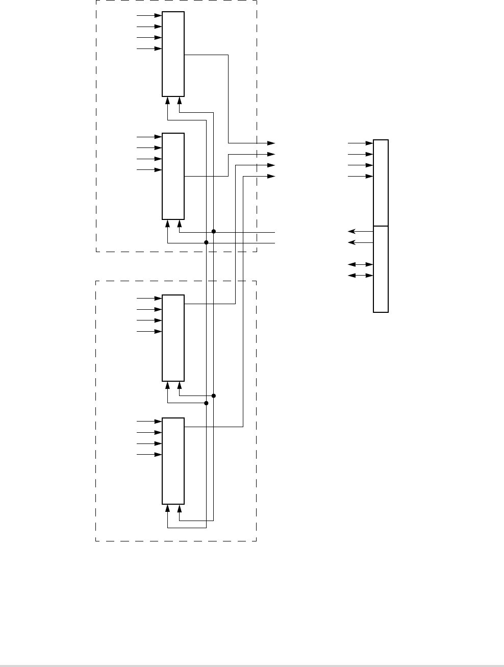
MOTOROLA Chapter 27. Queued Analog-to-Digital Converter (QADC) 27-33
Functional Description
Figure 27-18. External Multiplexing Configuration
When externally multiplexed mode is selected, the QADC automatically drives the MA
output signals from the channel number in each CCW. The QADC also converts the proper
input channel (ANW, ANX, ANY, and ANZ) by interpreting the CCW channel number. As
a result, up to 16 externally multiplexed channels appear to the conversion queues as
AN52/MA0/PQA0
AN53/MA1/PQA1
AN55/ETRIG1PQA3
AN56/ETRIG2/PQA4
AN0/ANW/PQB0
AN1/ANX/PQB1
AN2/ANY/PQB2
AN3/ANZ/PQB3
Port QBPort QA
AN0
AN2
AN4
AN6
AN1
AN3
AN5
AN7
AN16
AN18
AN20
AN22
AN17
AN19
AN21
AN23 MUX
MUX
MUX
MUX

27-34 MCF5282 User’s Manual MOTOROLA
Functional Description
directly connected signals. User software simply puts the channel number of externally
multiplexed channels into CCWs.
Figure 27-18 shows that the two MA signals may also be analog input signals. When
external multiplexing is selected, none of the MA signals can be used for analog or digital
inputs. They become multiplexed address outputs and are unaffected by DDRQA[1:0].
27.7.2.2 Module Version Options
The number of available analog channels varies, depending on whether external
multiplexing is used. A maximum of eight analog channels are supported by the internal
multiplexing circuitry of the converter. Table 27-21 shows the total number of analog input
channels supported with 0 to 4 external multiplexer chips.
27.7.3 Analog Subsystem
This section describes the QADC analog subsystem, which includes the front-end analog
multiplexer and analog-to-digital converter.
27.7.3.1 Analog-to-Digital Converter Operation
The analog subsystem consists of the path from the input signals to the A/D converter
block. Signals from the queue control logic are fed to the multiplexer and state machine.
The end-of-conversion (EOC) signal and the successive approximation register (SAR)
reflect the result of the conversion. Figure 27-19 shows a block diagram of the QADC
analog subsystem.
Table 27-21. Analog Input Channels
Number of Analog Input Channels Available
Directly Connected + External Multiplexed = Total Channels 1, 2
1The external trigger inputs are not shared with two analog input signals.
2When external multiplexing is used, two input channels are configured as multiplexed address outputs,
and for each external multiplexer chip, one input channel is a multiplexed analog input.
No External Mux One External Mux Two External
Muxes
Three External
Muxes
Four External
Muxes
8 5 + 4 = 9 4 + 8 = 12 3 + 12 = 15 2 + 16 = 18
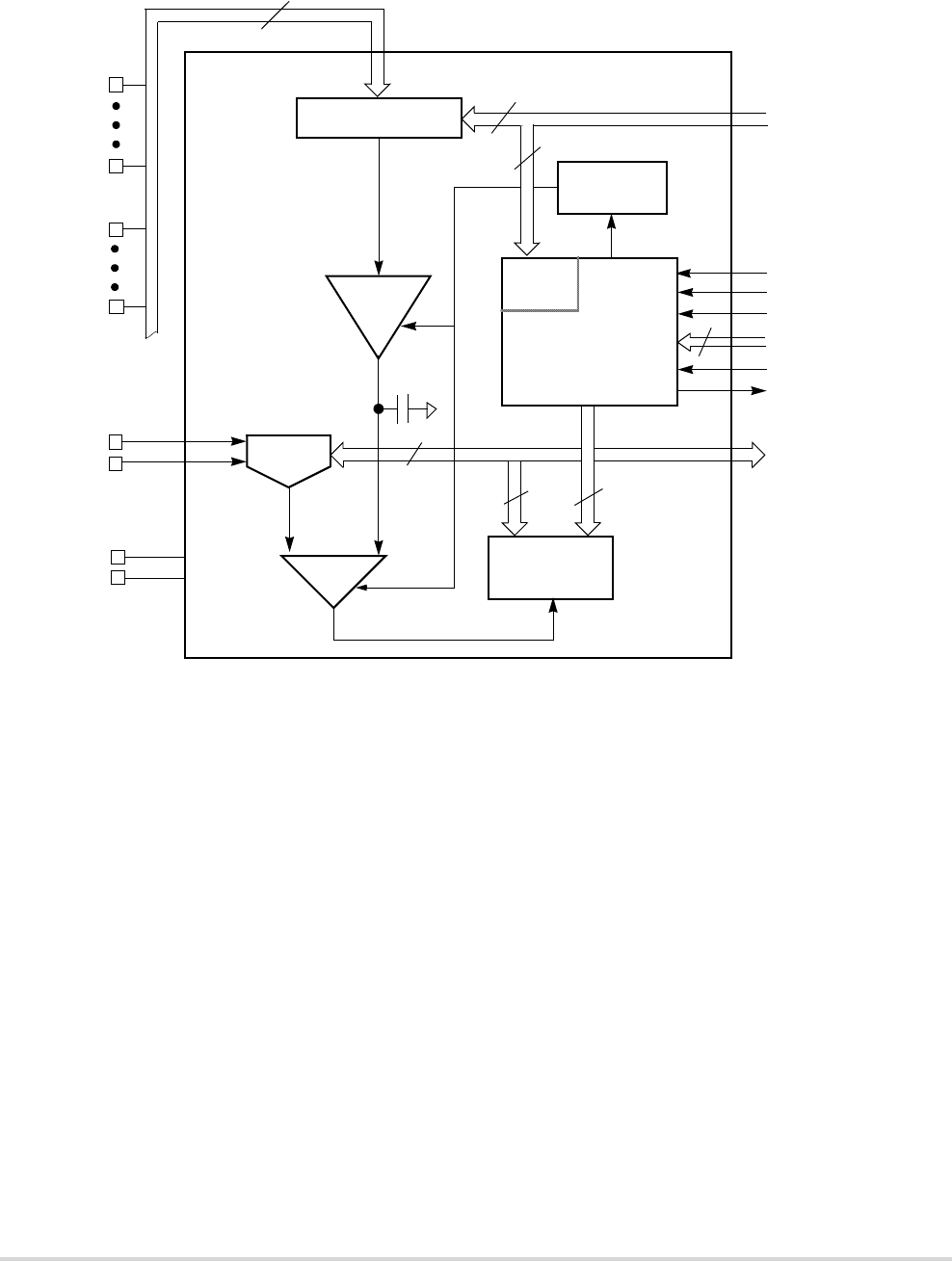
MOTOROLA Chapter 27. Queued Analog-to-Digital Converter (QADC) 27-35
Functional Description
Figure 27-19. QADC Analog Subsystem Block Diagram
27.7.3.2 Conversion Cycle Times
Total conversion time is made up of initial sample time, final sample time, and resolution
time. Initial sample time refers to the time during which the selected input channel is
coupled through the sample buffer amplifier to the sample capacitor. The sample buffer is
used to quickly reproduce its input signal on the sample capacitor and minimize charge
sharing errors. During the final sampling period the amplifier is bypassed, and the
multiplexer input charges the sample capacitor array directly for improved accuracy.
During the resolution period, the voltage in the sample capacitor is converted to a digital
value and stored in the SAR as shown in Figure 27-20.
Initial sample time is fixed at two QCLK cycles. Final sample time can be 2, 4, 8, or 16
QCLK cycles, depending on the value of the IST field in the CCW. Resolution time is 10
QCLK cycles.
A conversion requires a minimum of 14 QCLK cycles (7 µs with a 2.0-MHz QCLK). If the
maximum final sample time period of 16 QCLKs is selected, the total conversion time is
28 QCLKs or 14 µs (with a 2.0-MHz QCLK).
PQA4
PQA0
PQB3
PQB0
VDDA
VSSA
VRH
VRL
QCLK
Start Conv
End OF Conv
RST
STOP
SAR[9:0]
10-bit A/D Converter Input
Analog
Power
2
IST
Sample
Compar-
Successive
ator
Bias Circuit
Approximation
Register
Buffer
10
10
CHAN[5:0]
CSAMP
10
Chan. Decode & MUX
16:1
Signals From/to Queue Control Logic
16
State Machine & Logic
Power-
Down
Internal
Channel
Decode
SAR Timing
4
6
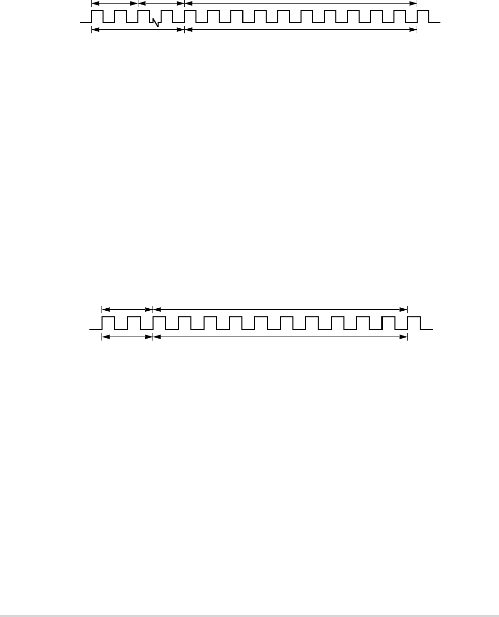
27-36 MCF5282 User’s Manual MOTOROLA
Functional Description
Figure 27-20. Conversion Timing
If the amplifier bypass mode is enabled for a conversion by setting the amplifier bypass
(BYP) field in the CCW, the timing changes to that shown in Figure 27-21. See
Section 27.6.7 for more information on the BYP field. The initial sample time is eliminated,
reducing the potential conversion time by two QCLKs. When using the bypass mode, the
external circuit should be of low source impedance (typically less than 10 kΩ). Also, the
loading effects on the external circuitry of the QADC need to be considered, because the
benefits of the sample amplifier are not present.
NOTE
Because of internal RC time constants, use of a two QCLK
sample time in bypass mode will cause serious errors when
operating the QADC at high frequencies.
Figure 27-21. Bypass Mode Conversion Timing
27.7.3.3 Channel Decode and Multiplexer
The internal multiplexer selects one of the eight analog input signals for conversion. The
selected input is connected to the sample buffer amplifier or to the sample capacitor. The
multiplexer also includes positive and negative stress protection circuitry, which prevents
deselected channels from affecting the selected channel when current is injected into the
deselected channels.
27.7.3.4 Sample Buffer
The sample buffer is used to raise the effective input impedance of the A/D converter, so
that external factors (higher bandwidth or higher impedance) are less critical to accuracy.
The input voltage is buffered onto the sample capacitor to reduce crosstalk between
channels.
Sample Time Successive Approximation Resolution Sequence
QCLK
Buffer
Sample
Time:
2 Cycles
Final
Sample
Time:
n Cycles
(2,4,8,16)
Resolution
Time:
10 Cycles
Sample Time Successive Approximation Resolution Sequence
QCLK
Sample
Time:
n CYCLES
(2,4,8,16)
Resolution
Time:
10 Cycles

MOTOROLA Chapter 27. Queued Analog-to-Digital Converter (QADC) 27-37
Digital Control Subsystem
27.7.3.5 Comparator
The comparator output feeds into the SAR, which accumulates the A/D conversion result
sequentially, beginning with the MSB.
27.7.3.6 Bias
The bias circuit is controlled by the STOP signal to power-up and power-down all the
analog circuits.
27.7.3.7 Successive Approximation Register (SAR)
The input of the SAR is connected to the comparator output. The SAR sequentially receives
the conversion value one bit at a time, starting with the MSB. After accumulating the 10
bits of the conversion result, the SAR data is transferred to the appropriate result location,
where it may be read by user software.
27.7.3.8 State Machine
The state machine generates all timing to perform an A/D conversion. An internal
start-conversion signal indicates to the A/D converter that the desired channel has been sent
to the MUX. CCW[IST[1:0]] denotes the desired sample time. CCW[BYP] determines
whether to bypass the sample amplifier. Once the end of conversion has been reached a
signal is sent to the queue control logic indicating that a result is available for storage in the
result RAM.
27.8 Digital Control Subsystem
The digital control subsystem includes the control logic to sequence the conversion activity,
the system clock and periodic/interval timer, control and status registers, the conversion
command word table RAM, and the result word table RAM.
The central element for control of QADC conversions is the 64-entry conversion command
word (CCW) table. Each CCW specifies the conversion of one input channel. Depending
on the application, one or two queues can be established in the CCW table. A queue is a
scan sequence of one or more input channels. By using a pause mechanism, subqueues can
be created in the two queues. Each queue can be operated using one of several different scan
modes. The scan modes for queue 1 and queue 2 are programmed in control registers
QACR1 and QACR2. Once a queue has been started by a trigger event (any of the ways to
cause the QADC to begin executing the CCWs in a queue or subqueue), the QADC
performs a sequence of conversions and places the results in the result word table.

27-38 MCF5282 User’s Manual MOTOROLA
Digital Control Subsystem
27.8.1 Queue Priority Timing Examples
This subsection describes the QADC priority scheme when trigger events on two queues
overlap or conflict.
27.8.1.1 Queue Priority
Queue 1 has priority over queue 2 execution. These cases show the conditions under which
queue 1 asserts its priority:
• When a queue is not active, a trigger event for queue 1 or queue 2 causes the
corresponding queue execution to begin.
• When queue 1 is active and a trigger event occurs for queue 2, queue 2 cannot begin
execution until queue 1 reaches completion or the paused state. The status register
records the trigger event by reporting the queue 2 status as trigger pending.
Additional trigger events for queue 2, which occur before execution can begin, are
flagged as trigger overruns.
• When queue 2 is active and a trigger event occurs for queue 1, the current queue 2
conversion is aborted. The status register reports the queue 2 status as suspended.
Any trigger events occurring for queue 2 while it is suspended are flagged as trigger
overruns. Once queue 1 reaches the completion or the paused state, queue 2 begins
executing again. The programming of the RESUME bit in QACR2 determines
which CCW is executed in queue 2.
• When simultaneous trigger events occur for queue 1 and queue 2, queue 1 begins
execution and the queue 2 status is changed to trigger pending.
• When subqueues are paused
The pause feature can be used to divide queue 1 and/or queue 2 into multiple subqueues. A
subqueue is defined by setting the pause bit in the last CCW of the subqueue.
Figure 27-22 shows the CCW format and an example of using pause to create subqueues.
Queue 1 is shown with four CCWs in each subqueue and queue 2 has two CCWs in each
subqueue.
The operating mode selected for queue 1 determines what type of trigger event causes the
execution of each of the subqueues within queue 1. Similarly, the operating mode for queue
2 determines the type of trigger event required to execute each of the subqueues within
queue 2.
For example, when the external trigger rising edge continuous-scan mode is selected for
queue 1, and there are six subqueues within queue 1, a separate rising edge is required on
the external trigger signal after every pause to begin the execution of each subqueue (refer
to Figure 27-22).
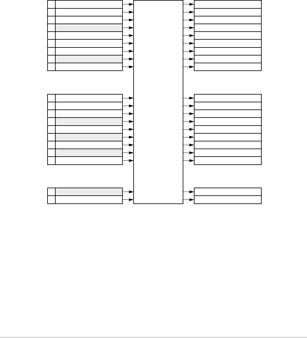
MOTOROLA Chapter 27. Queued Analog-to-Digital Converter (QADC) 27-39
Digital Control Subsystem
The choice of single-scan or continuous-scan applies to the full queue, and is not applied to
each subqueue. Once a subqueue is initiated, each CCW is executed sequentially until the
last CCW in the subqueue is executed and the pause state is entered. Execution can only
continue with the next CCW, which is the beginning of the next subqueue. A subqueue
cannot be executed a second time before the overall queue execution has been completed.
Figure 27-22. QADC Queue Operation with Pause
Trigger events which occur during the execution of a subqueue are ignored, but the trigger
overrun flag is set. When a continuous-scan mode is selected, a trigger event occurring after
the completion of the last subqueue (after the queue completion flag is set), causes the
execution to continue with the first subqueue, starting with the first CCW in the queue.
When the QADC encounters a CCW with the pause bit set, the queue enters the paused state
after completing the conversion specified in the CCW with the pause bit. The pause flag is
set in QASR0, and a pause interrupt may be requested. The status of the queue is shown to
be paused, indicating completion of a subqueue. The QADC then waits for another trigger
event to again begin execution of the next subqueue.
Beginning of Queue 1 00
Channel Select,
Sample, Hold,
A/D Conversion
Conversion Command
Result Word Table
0
Pause
Word (CCW) Table
0
0
1
0
0
0
1
0
Pause
00
P
0
Pause
0
0
1
0
1
0
1
0
Pause
P
End of Queue 1
Beginning of Queue 2
B
Q2
Pause
Pause
End of Queue 2
P
1
063 63
•
•
•
•
•
•
•
•
•
•
•
•

27-40 MCF5282 User’s Manual MOTOROLA
Digital Control Subsystem
27.8.1.2 Queue Priority Schemes
Because there are two conversion command queues and only one A/D converter, a priority
scheme determines which conversion occurs. Each queue has a variety of trigger events that
are intended to initiate conversions, and they can occur asynchronously in relation to each
other and other conversions in progress. For example, a queue can be idle awaiting a trigger
event; a trigger event can have occurred, but the first conversion has not started; a
conversion can be in progress; a pause condition can exist awaiting another trigger event to
continue the queue; and so on.
The following paragraphs and figures outline the prioritizing criteria used to determine
which conversion occurs in each overlap situation.
NOTE
Each situation in Figure 27-23 through Figure 27-33 is labeled
S1 through S19. In each diagram, time is shown increasing
from left to right. The execution of queue 1 and queue 2 (Q1
and Q2) is shown as a string of rectangles representing the
execution time of each CCW in the queue. In most of the
situations, there are four CCWs (labeled C1 to C4) in both
queue 1 and queue 2. In some of the situations, CCW C2 is
presumed to have the pause bit set, to show the similarities of
pause and end-of-queue as terminations of queue execution.
Trigger events are described in Table 27-22.
When a trigger event causes a CCW execution in progress to be aborted, the aborted
conversion is shown as a ragged end of a shortened CCW rectangle.
The situation diagrams also show when key status bits are set.
Table 27-23 describes the status bits.
Table 27-22. Trigger Events
Trigger Events
T1 Events that trigger queue 1 execution (external trigger, software-initiated single-scan enable
bit, or completion of the previous continuous loop)
T2 Events that trigger queue 2 execution (external trigger, software-initiated single-scan enable
bit, timer period/interval expired, or completion of the previous continuous loop)
Table 27-23. Status Bits
Bit Function
CF flag Set when the end of the queue is reached
PF flag Set when a queue completes execution up through a pause bit
Trigger overrun
error (TOR)
Set when a new trigger event occurs before the queue is finished servicing the
previous trigger event
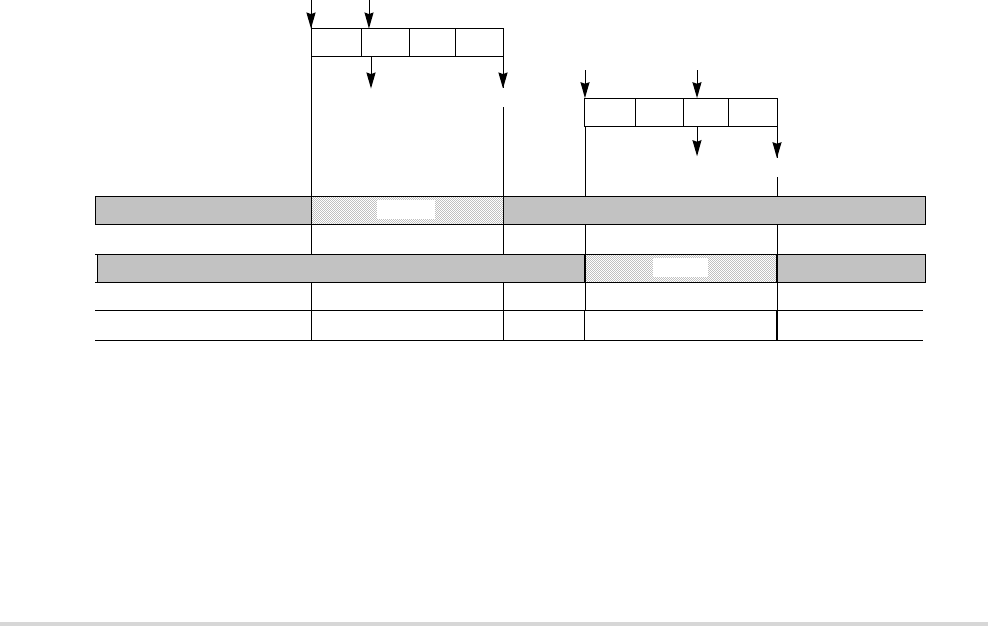
MOTOROLA Chapter 27. Queued Analog-to-Digital Converter (QADC) 27-41
Digital Control Subsystem
Below the queue execution flows are three sets of blocks that show the status information
that is made available to the user. The first two rows of status blocks show the condition of
each queue as:
• Idle
•Active
•Pause
• Suspended (queue 2 only)
• Trigger pending
The third row of status blocks shows the 4-bit QS status register field that encodes the
condition of the two queues. Two transition status cases, QS = 0011 and QS = 0111, are not
shown because they exist only very briefly between stable status conditions.
The first three examples in Figure 27-23 through Figure 27-25 (S1, S2, and S3) show what
happens when a new trigger event is recognized before the queue has completed servicing
the previous trigger event on the same queue.
In situation S1 (Figure 27-23), one trigger event is being recognized on each queue while
that queue is still working on the previously recognized trigger event. The trigger overrun
error status bit is set, and the premature trigger event is otherwise ignored. A trigger event
that occurs before the servicing of the previous trigger event is through does not disturb the
queue execution in progress.
Figure 27-23. CCW Priority Situation 1
In situation S2 (Figure 27-24), more than one trigger event is recognized before servicing
of a previous trigger event is complete. The trigger overrun bit is again set, but the
additional trigger events are otherwise ignored. After the queue is complete, the first newly
detected trigger event causes queue execution to begin again. When the trigger event rate
is high, a new trigger event can be seen very soon after completion of the previous queue,
Q1:
Q2:
QS:
IDLE
IDLE ACTIVE IDLE
0000 1000 0000 0010 0000
TOR1
T1 T1
Q1: C1 C2 C3 C4
CF1
C1 C2 C3 C4
TOR2
T2 T2
Q2:
CF2
IDLE
ACTIVE
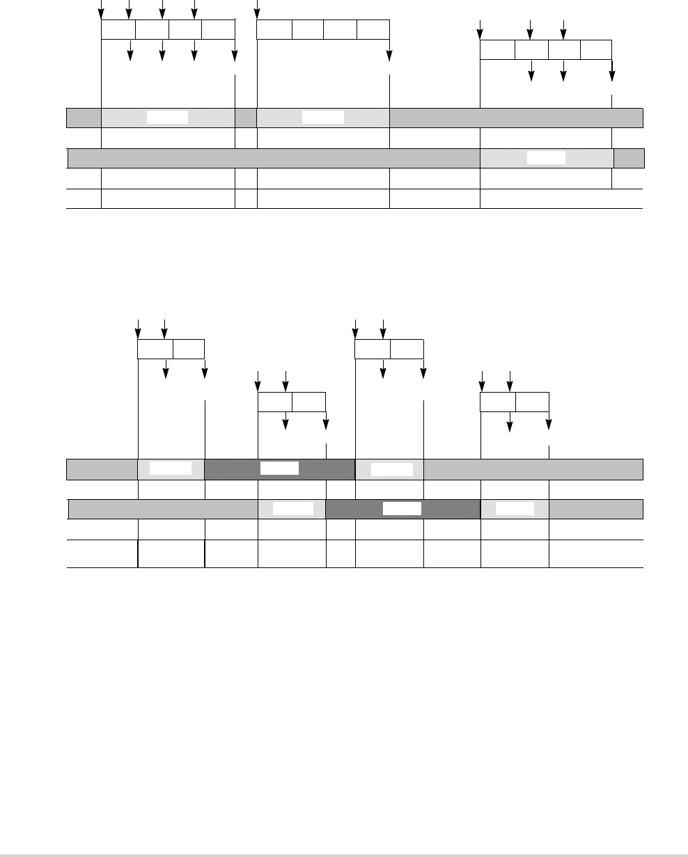
27-42 MCF5282 User’s Manual MOTOROLA
Digital Control Subsystem
leaving little time to retrieve the previous results. Also, when trigger events are occurring
at a high rate for queue 1, the lower priority queue 2 channels may not get serviced at all.
Figure 27-24. CCW Priority Situation 2
Situation S3 (Figure 27-25) shows that when the pause feature is used, the trigger overrun
error status bit is set the same way and that queue execution continues unchanged.
Figure 27-25. CCW Priority Situation 3
The next two situations consider trigger events that occur for the lower priority queue 2,
while queue 1 is actively being serviced.
Situation S4 (Figure 27-26) shows that a queue 2 trigger event is recognized while queue 1
is active is saved, and as soon as queue 1 is finished, queue 2 servicing begins.
T1
ACTIVE IDLE
Q1:
Q2:
QS:
IDLE ACTIVE
IDLE ACTIVE IDLE
1000 1000 0000 0010 0000
C1 C2 C3 C4
TOR2
T2 T2
Q2:
CF2
IDLE
C1 C2 C3 C4
T1
CF1
C1 C2 C3 C4
TOR1
T1
Q1:
CF1
TOR1
T1
TOR1
T1
TOR2
T2
PAUSE
Q1:
Q2:
QS:
IDLE ACTIVE
IDLE ACTIVE IDLE
1000 0110 0001 0010
ACTIVE
0000
IDLE
C1 C2
T1 T1
Q1:
TOR1 PF1
C1 C2
0000
Q2:
0100
TOR2 PF2
T2 T2
0101
C3 C4
T1 T1
TOR1 CF1
ACTIVE
PAUSE
1001
C3 C4
CF2
T2 T2
TOR2
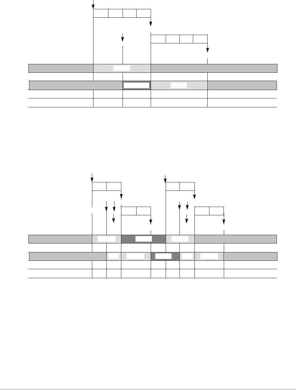
MOTOROLA Chapter 27. Queued Analog-to-Digital Converter (QADC) 27-43
Digital Control Subsystem
Figure 27-26. CCW Priority Situation 4
Situation S5 (Figure 27-27) shows that when multiple queue 2 trigger events are detected
while queue 1 is busy, the trigger overrun error bit is set, but queue 1 execution is not
disturbed. Situation S5 also shows that the effect of queue 2 trigger events during queue 1
execution is the same when the pause feature is used for either queue.
Figure 27-27. CCW Priority Situation 5
The remaining situations, S6 through S11, show the impact of a queue 1 trigger event
occurring during queue 2 execution. Because queue 1 has higher priority, the conversion
taking place in queue 2 is aborted so that there is no variable latency time in responding to
queue 1 trigger events.
In situation 6 (Figure 27-28), the conversion initiated by the second CCW in queue 2 is
aborted just before the conversion is complete, so that queue 1 execution can begin. Queue
2 is considered suspended. After queue 1 is finished, queue 2 starts over with the first CCW,
Q1:
Q2:
QS:
IDLE
IDLE ACTIVE IDLE
0000 1000 0010
ACTIVE
0000
C1 C2 C3 C4
T1
Q1:
CF1
Q2:
C1 C2 C3 C4
T2
CF2
IDLE
1011
TRIGGERED
Q1:
Q2:
QS:
IDLE
IDLE IDLE
0000 1000 0010
ACTIVE
0000
C1 C2
T1
Q1:
C1 C2
PF2
C3 C4
C3 C4
CF2
IDLE
1011
TRIG
Q2:
T2T2 PF1
PAUSE
ACTIVE PAUSE
TOR2
T2T2 CF1
TOR2
T1
ACTIVE
TRIG
0110
ACTIVE
ACTIVE
0101 1001 1011
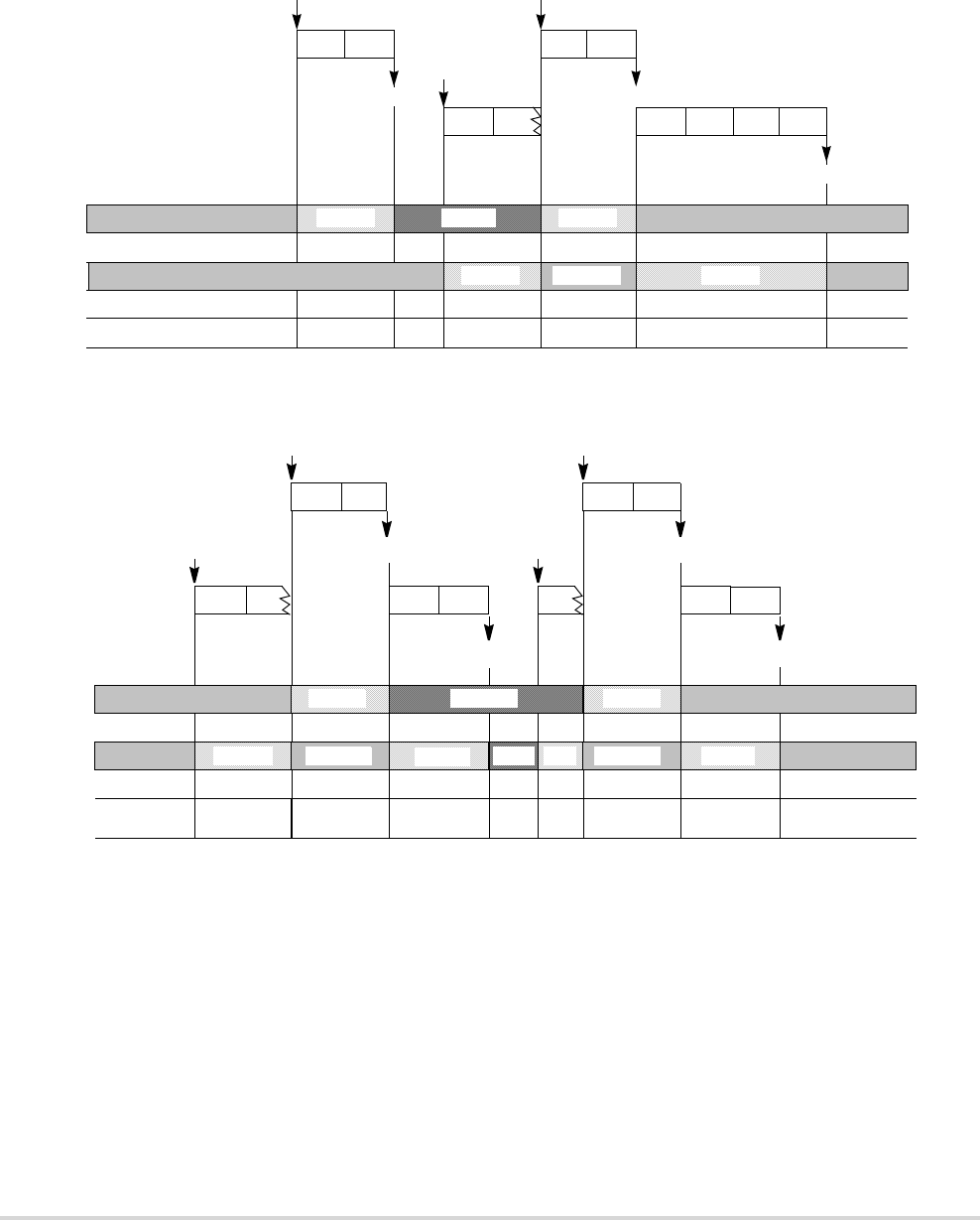
27-44 MCF5282 User’s Manual MOTOROLA
Digital Control Subsystem
when the RESUME control bit is set to 0. Situation S7 (Figure 27-29) shows that when
pause operation is not used with queue 2, queue 2 suspension works the same way.
Figure 27-28. CCW Priority Situation 6
.
Figure 27-29. CCW Priority Situation 7
Situations S8 and S9 (Figure 27-30 and Figure 27-31) repeat the same two situations with
the RESUME bit set to a 1. When the RESUME bit is set, following suspension, queue 2
resumes execution with the aborted CCW, not the first CCW, in the queue.
IDLE
Q1:
Q2:
QS
IDLE
IDLE
0000 1000
ACTIVE
C1 C2
T1
Q1:
C1
C3 C4
IDLE
Q2:
PF1
PAUSE
ACTIVE
CF1
T1
ACTIVE
SUSPEND
0100
ACTIVE
ACTIVE
0110 1010
C1 C2 C3 C4
CF2
T2
0010 0000
RESUME = 0
C2
T1
PAUSE
Q1:
Q2:
QS:
IDLE ACTIVE
IDLE ACTIVE IDLE
0010 0110 1010 0010
ACTIVE
0000
IDLE
Q1:
PF1
C1 C2
0000 1010
ACTIVE
0110
C1
Q2:
T2
C1
PF2
T1
C3 C4
CF1
C3
CF2
SUSPEND PAUSE SUSPEND
T2
C1 C3
C2
ACTIVE ACT
0101
C4
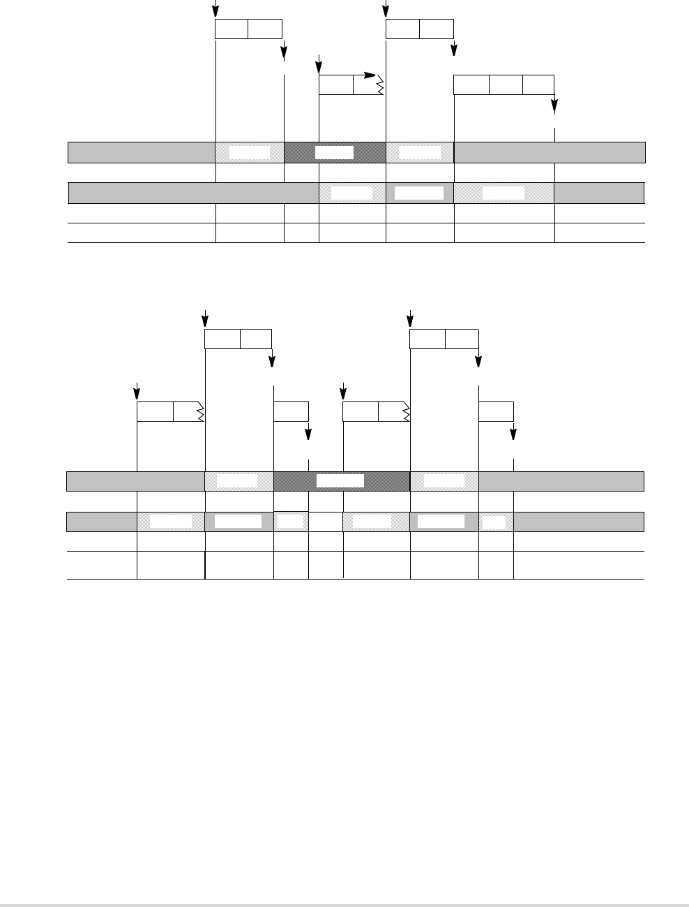
MOTOROLA Chapter 27. Queued Analog-to-Digital Converter (QADC) 27-45
Digital Control Subsystem
Figure 27-30. CCW Priority Situation 8
Figure 27-31. CCW Priority Situation 9
Situations S10 and S11 (Figure 27-32 and Figure 27-33) show that when an additional
trigger event is detected for queue 2 while the queue is suspended, the trigger overrun error
bit is set, the same as if queue 2 were being executed when a new trigger event occurs.
Trigger overrun on queue 2 thus allows the user to know that queue 1 is taking up so much
QADC time that queue 2 trigger events are being lost.
IDLE
Q1:
Q2:
QS:
IDLE
IDLE
0000 1000 0010
ACTIVE
C1 C2
T1
Q1:
C1
C3 C4
IDLE
Q2:
PF1
PAUSE
ACTIVE
CF1
T1
ACTIVE
SUSPEND
0100
ACTIVE
ACTIVE
0110 1010
C2 C3 C4
CF2
T2
0000
RESUME=1
C2
T1
PAUSE
Q1:
Q2:
QS:
IDLE ACTIVE
IDLE ACT IDLE
0010 0110 1010 0010
ACTIVE
0000
IDLE
Q1:
PF1
C1 C2
0000 1010 0101
ACTIVE
PAUSE
0110
C1
Q2:
T2
C2
PF2
T1
C3 C4
CF1
C4
CF2
SUSPEND ACT ACTIVE SUSPEND
T2
C3C1 RESUME=1
C2 C4
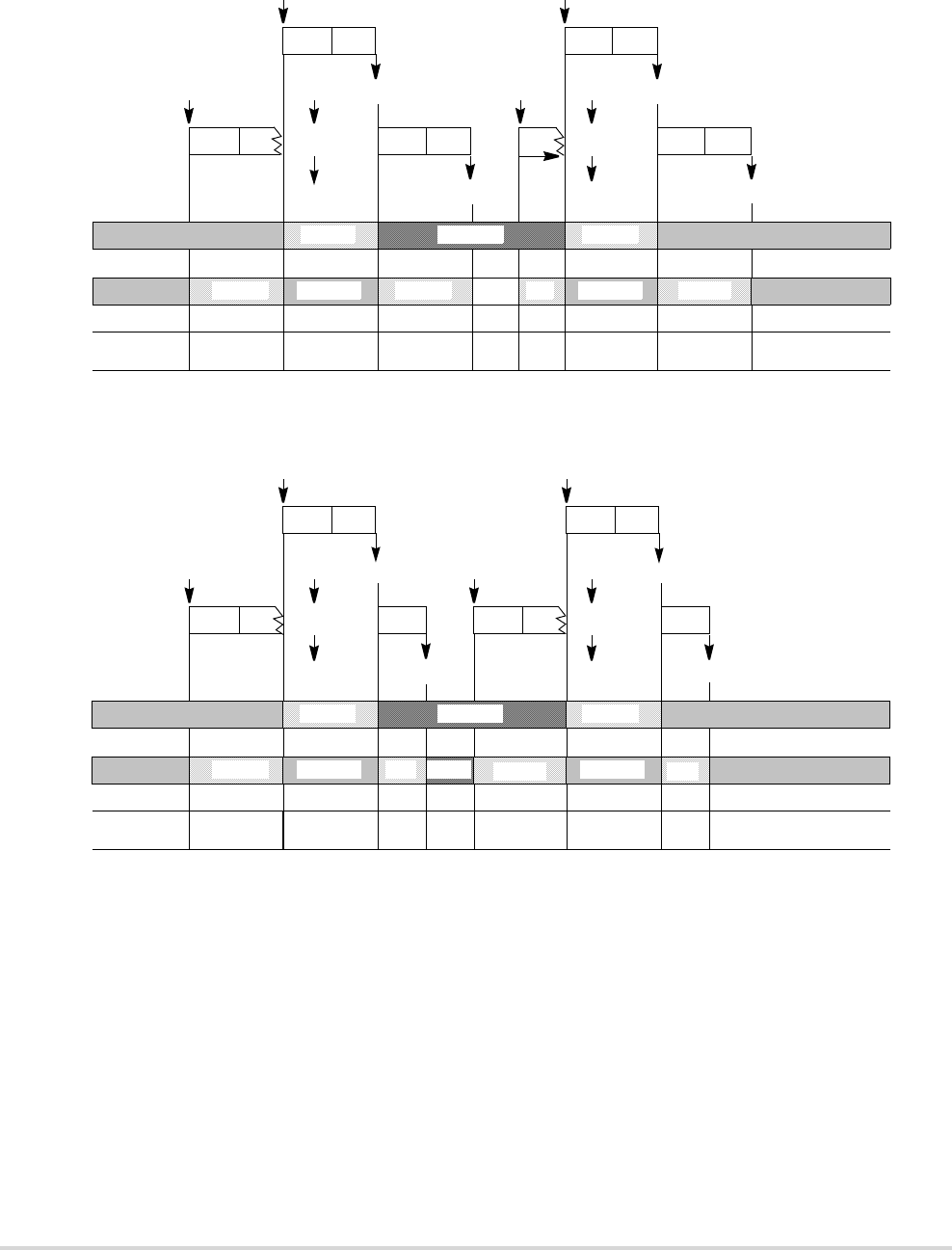
27-46 MCF5282 User’s Manual MOTOROLA
Digital Control Subsystem
Figure 27-32. CCW Priority Situation 10
Figure 27-33. CCW Priority Situation 11
The previous situations cover normal overlap conditions that arise with asynchronous
trigger events on the two queues. An additional conflict to consider is that the freeze
condition can arise while the QADC is actively executing CCWs. The conventional use for
the debug mode is for software/hardware debugging. When the CPU enters background
debug mode, peripheral modules can cease operation. When freeze is detected, the QADC
completes the conversion in progress, unlike the abort that occurs when queue 1 suspends
queue 2. After the freeze condition is removed, the QADC continues queue execution with
the next CCW in sequence.
Trigger events that occur during freeze are not captured. When a trigger event is pending
for queue 2 before freeze begins, that trigger event is remembered when the freeze is
T1 T1
PAUSE
Q1:
Q2:
QS:
IDLE ACTIVE
IDLE ACTIVE IDLE
0010 0110 1010 0010
ACTIVE
0000
IDLE
Q1:
PF1
C1 C2
0000 1010 0101
ACTIVE
PAU SE
0110
Q2:
T2
PF2
C1 C2
C3 C4
CF1
C3 C4
CF2
T2
C3
SUSPEND ACTIVE
C1
ACT SUSPEND
T2
TOR2
T2
TOR2
RESUME = 0
C2
T1 T1
C3 C4
CF1
PAUSE
Q1:
Q2:
QS:
IDLE ACTIVE
IDLE ACT IDLE
0010 0110 1010 0010
ACTIVE
0000
IDLE
Q1:
PF1
C1 C2
0000 1010 0101
ACTIVE
PAUSE
0110
Q2:
T2
SUSPEND ACT
C1
ACTIVE SUSPEND
T2
TOR2
T2
TOR2
C2
PF2
C4
CF2
T2
C3
C2 C4 RESUME = 1
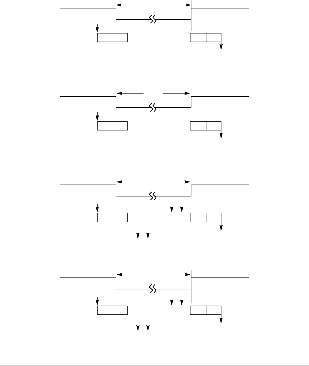
MOTOROLA Chapter 27. Queued Analog-to-Digital Converter (QADC) 27-47
Digital Control Subsystem
passed. Similarly, when freeze occurs while queue 2 is suspended, after freeze, queue 2
resumes execution as soon as queue 1 is finished.
Situations 12 through 19 (Figure 27-34 to Figure 27-41) show examples of all of the freeze
situations.
Figure 27-34. CCW Freeze Situation 12
Figure 27-35. CCW Freeze Situation 13
Figure 27-36. CCW Freeze Situation 14
Figure 27-37. . CCW Freeze Situation 15
C3 C4
CF1
C1 C2
T1
Q1:
FREEZE
C1 C2
T2
Q2:
CF2
C3 C4
FREEZE
C1 C2
T1
Q1:
CF1
C3 C4
FREEZE
T1 T1
T2 T2
TRIGGERS IGNORED
C1 C2
T2
Q2:
CF2
C3 C4
FREEZE
T2 T2
T1 T1
TRIGGERS IGNORED
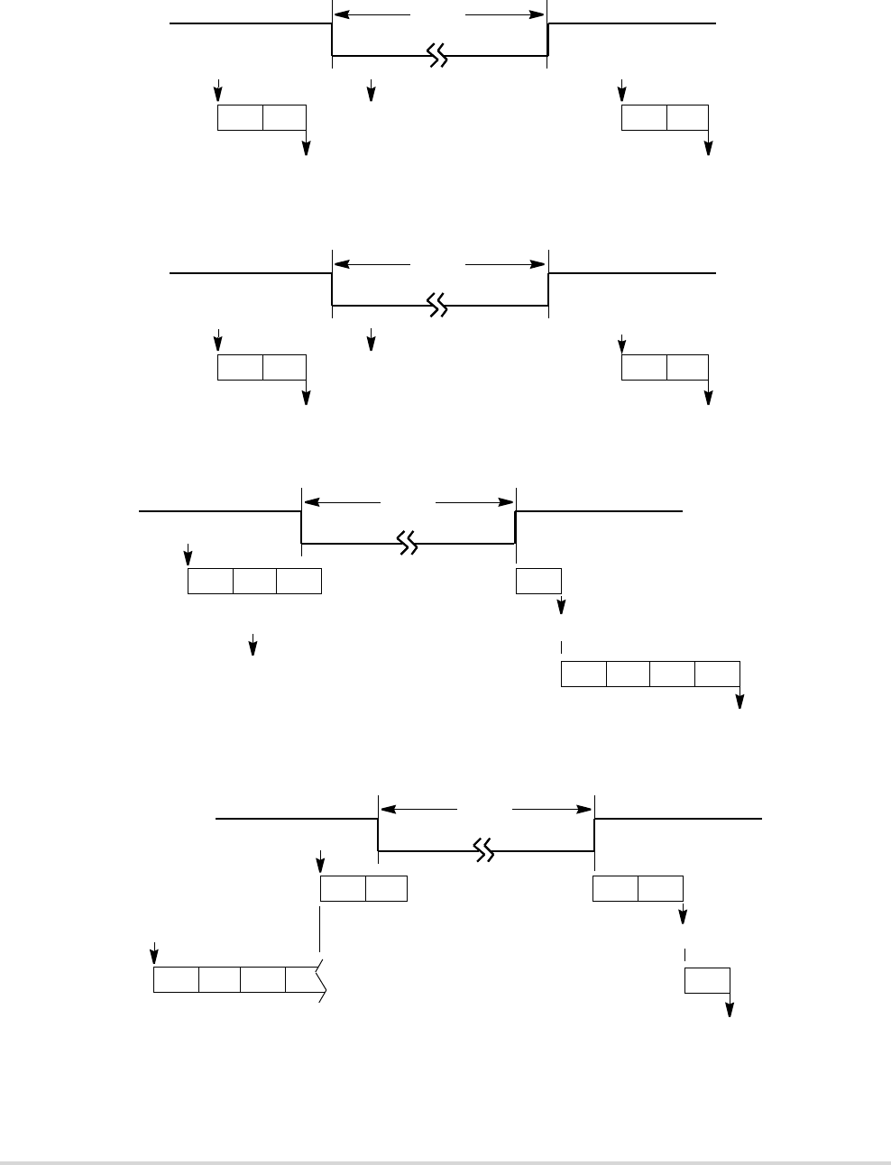
27-48 MCF5282 User’s Manual MOTOROLA
Digital Control Subsystem
Figure 27-38. CCW Freeze Situation 16
Figure 27-39. CCW Freeze Situation 17
Figure 27-40. CCW Freeze Situation 18
Figure 27-41. CCW Freeze Situation 19
C1 C2
T1
Q1:
CF1
C3 C4
FREEZE
T1 T1
PF1
TRIGGERS IGNORED
C1 C2
T2
Q2:
CF2
C3 C4
FREEZE
T2 T2
PF2
TRIGGERS IGNORED
C1 C2
T1
Q1:
CF1
C3 C4
FREEZE
T2
C1 C2
Q2: C3
CF2
C4
TRIGGER CAPTURED, RESPONSE DELAYED AFTER FREEZE
C1 C2
T1
Q1:
CF1
C4
FREEZE
CF2
C4
C1 C2
T2
Q2: C3
C3
C4

MOTOROLA Chapter 27. Queued Analog-to-Digital Converter (QADC) 27-49
Digital Control Subsystem
27.8.2 Boundary Conditions
The queue operation boundary conditions are:
• The first CCW in a queue specifies channel 63, the end-of-queue (EOQ) code. The
queue becomes active and the first CCW is read. The end-of-queue is recognized,
the completion flag is set, and the queue becomes idle. A conversion is not
performed.
• BQ2 (beginning of queue 2) is set at the end of the CCW table (63) and a trigger
event occurs on queue 2. The end-of-queue condition is recognized, a conversion is
performed, the completion flag is set, and the queue becomes idle.
• BQ2 is set to CCW0 and a trigger event occurs on queue 1. After reading CCW0,
the end-of-queue condition is recognized, the completion flag is set, and the queue
becomes idle. A conversion is not performed.
• BQ2 (beginning of queue 2) is set beyond the end of the CCW table (64–127) and a
trigger event occurs on queue 2. The end-of-queue condition is recognized
immediately, the completion flag is set, and the queue becomes idle. A conversion
is not performed.
NOTE
Multiple end-of-queue conditions may be recognized
simultaneously, although there is no change in QADC
behavior. For example, if BQ2 is set to CCW0, CCW0 contains
the EOQ code, and a trigger event occurs on queue 1, the
QADC reads CCW0 and detects both end-of-queue conditions.
The completion flag is set and queue 1 becomes idle.
Boundary conditions also exist for combinations of pause and end-of-queue. One case is
when a pause bit is in one CCW and an end-of-queue condition is in the next CCW. The
conversion specified by the CCW with the pause bit set completes normally. The pause flag
is set. However, because the end-of-queue condition is recognized, the completion flag is
also set and the queue status becomes idle, not paused. Examples of this situation include:
• The pause bit is set in CCW5 and the channel 63 (EOQ) code is in CCW6.
• The pause is in CCW63.
• During queue 1 operation, the pause bit is set in CCW20 and BQ2 points to CCW21.
Another pause and end-of-queue boundary condition occurs when the pause and an
end-of-queue condition occur in the same CCW. Both the pause and end-of-queue
conditions are recognized simultaneously. The end-of-queue condition has precedence so a
conversion is not performed for the CCW and the pause flag is not set. The QADC sets the
completion flag and the queue status becomes idle. Examples of this situation are:
• The pause bit is set in CCW10 and EOQ is programmed into CCW10.
• During queue 1 operation, the pause bit set in CCW32, which is also BQ2.

27-50 MCF5282 User’s Manual MOTOROLA
Digital Control Subsystem
27.8.3 Scan Modes
The QADC queuing mechanism allows application software to utilize different
requirements for automatically scanning input channels.
In single-scan mode, a single pass through a sequence of conversions defined by a queue is
performed. In continuous-scan mode, multiple passes through a sequence of conversions
defined by a queue are executed.
The possible modes are:
• Disabled mode and reserved mode
• Software-initiated single-scan mode
• Externally triggered single-scan mode
• Externally gated single-scan mode
• Interval timer single-scan mode
• Software-initiated continuous-scan mode
• Externally triggered continuous-scan mode
• Externally gated continuous-scan mode
• Periodic timer continuous-scan mode
The following paragraphs describe single-scan and continuous-scan operations.
27.8.4 Disabled Mode
When disabled mode is selected, the queue is not active. Trigger events cannot initiate
queue execution. When both queue 1 and queue 2 are disabled, there is no possibility of
encountering wait states when accessing CCW table and result RAM. When both queues
are disabled, it is safe to change the QCLK prescaler values.
27.8.5 Reserved Mode
Reserved mode is available for future mode definitions. When reserved mode is selected,
the queue is not active. The behavior is the same as disabled mode.
27.8.6 Single-Scan Modes
A single-scan queue operating mode is used to execute a single pass through a sequence of
conversions defined by a queue. By programming the MQ1 field in QACR1 or the MQ2
field in QACR2, these modes can be selected:
• Software-initiated single-scan mode
• Externally triggered single-scan mode

MOTOROLA Chapter 27. Queued Analog-to-Digital Converter (QADC) 27-51
Digital Control Subsystem
• Externally gated single-scan mode
• Interval timer single-scan mode
NOTE
Queue 2 cannot be programmed for externally gated
single-scan mode.
In all single-scan queue operating modes, queue execution is enabled by writing the
single-scan enable bit to a 1 in the queue’s control register. The single-scan enable bits,
SSE1 and SSE2, are provided for queue 1 and queue 2, respectively.
Until a queue’s single-scan enable bit is set, any trigger events for that queue are ignored.
The single-scan enable bit may be set to a 1 during the same write cycle that selects the
single-scan queue operating mode. The single-scan enable bit can be written only to 1, but
will always read 0. Once set, writing the single-scan enable bit to 0 has no effect. Only the
QADC can clear the single-scan enable bit. The completion flag, completion interrupt, or
queue status is used to determine when the queue has completed.
After the single-scan enable bit is set, a trigger event causes the QADC to begin execution
with the first CCW in the queue. The single-scan enable bit remains set until the queue is
completed. After the queue reaches completion, the QADC resets the single-scan enable bit
to 0. Writing the single-scan enable bit to a 1 or a 0 before the queue scan is complete has
no effect; however, if the queue operating mode is changed, the new queue operating mode
and the value of the single-scan enable bit are recognized immediately. The conversion in
progress is aborted, and the new queue operating mode takes effect.
In software-initiated single-scan mode, writing a 1 to the single-scan enable bit causes the
QADC to generate a trigger event internally, and queue execution begins immediately. In
the other single-scan queue operating modes, once the single-scan enable bit is written, the
selected trigger event must occur before the queue can start. The single-scan enable bit
allows the entire queue to be scanned once. A trigger overrun is captured if a trigger event
occurs during queue execution in an edge-sensitive external trigger mode or a
periodic/interval timer mode.
In the interval timer single-scan mode, the next expiration of the timer is the trigger event
for the queue. After queue execution is complete, the queue status is shown as idle. The
queue can be restarted by setting the single-scan enable bit to 1. Queue execution begins
with the first CCW in the queue.
27.8.6.1 Software-Initiated Single-Scan Mode
Software can initiate the execution of a scan sequence for queue 1 or 2 by selecting
software-initiated single-scan mode and writing the single-scan enable bit in QACR1 or
QACR2. A trigger event is generated internally and the QADC immediately begins

27-52 MCF5282 User’s Manual MOTOROLA
Digital Control Subsystem
execution of the first CCW in the queue. If a pause occurs, another trigger event is
generated internally, and then execution continues without pausing.
The QADC automatically performs the conversions in the queue until an end-of-queue
condition is encountered. The queue remains idle until the single-scan enable bit is again
set. While the time to internally generate and act on a trigger event is very short, the queue
status field can be read as momentarily indicating that the queue is paused. The trigger
overrun flag is never set while in software-initiated single-scan mode.
The software-initiated single-scan mode is useful when:
• Complete control of queue execution is required
• There is a need to easily alternate between several queue sequences
27.8.6.2 Externally Triggered Single-Scan Mode
The externally triggered single-scan mode is available on both queue 1 and queue 2. Both
rising and falling edge triggered modes are available. A scan must be enabled by setting the
single-scan enable bit for the queue.
The first external trigger edge causes the queue to be executed one time. Each CCW is read
and the indicated conversions are performed until an end-of-queue condition is
encountered. After the queue is completed, the QADC clears the single-scan enable bit. The
single-scan enable bit can be written again to allow another scan of the queue to be initiated
by the next external trigger edge.
The externally triggered single-scan mode is useful when the input trigger rate can exceed
the queue execution rate. Analog samples can be taken in sync with an external event, even
though application software does not require data taken from every edge. Externally
triggered single-scan mode can be enabled to get one set of data and, at a later time, be
enabled again for the next set of samples.
When a pause bit is encountered during externally triggered single-scan mode, another
trigger event is required for queue execution to continue. Software involvement is not
required for queue execution to continue from the paused state.
27.8.6.3 Externally Gated Single-Scan Mode
The QADC provides external gating for queue 1 only. When externally gated single-scan
mode is selected, the input level on the associated external trigger signal enables and
disables queue execution. The polarity of the external gate signal is fixed so that only a high
level opens the gate and a low level closes the gate. Once the gate is open, each CCW is
read and the indicated conversions are performed until the gate is closed. Queue scan must
be enabled by setting the single-scan enable bit for queue 1. If a pause is encountered, the
pause flag does not set, and execution continues without pausing.

MOTOROLA Chapter 27. Queued Analog-to-Digital Converter (QADC) 27-53
Digital Control Subsystem
While the gate is open, queue 1 executes one time. Each CCW is read and the indicated
conversions are performed until an end-of-queue condition is encountered. When queue 1
completes, the QADC sets the completion flag (CF1) and clears the single-scan enable bit.
Set the single-scan enable bit again to allow another scan of queue 1 to be initiated during
the next open gate.
If the gate closes before queue 1 completes execution, the current CCW completes,
execution of queue 1 stops, the single-scan enable bit is cleared, and the PF1 bit is set. The
CWPQ1 field can be read to determine the last valid conversion in the queue. The
single-scan enable bit must be set again and the PF1 bit should be cleared before another
scan of queue 1 is initiated during the next open gate. The start of queue 1 is always the first
CCW in the CCW table.
Because the gate level is only sampled after each conversion during queue execution,
closing the gate for a period less than a conversion time interval does not guarantee the
closure will be captured.
27.8.6.4 Interval Timer Single-Scan Mode
Both queues can use the periodic/interval timer in a single-scan queue operating mode. The
timer interval can range from 27 to 217 QCLK cycles in binary multiples. When the interval
timer single-scan mode is selected and the single-scan enable bit is set in QACR1 or
QACR2, the timer begins counting. When the time interval elapses, an internal trigger
event is generated to start the queue and the QADC begins execution with the first CCW.
The QADC automatically performs the conversions in the queue until a pause or an
end-of-queue condition is encountered. When a pause occurs, queue execution stops until
the timer interval elapses again, and queue execution continues. When queue execution
reaches an end-of-queue situation, the single-scan enable bit is cleared. Set the single-scan
enable bit again to allow another scan of the queue to be initiated by the interval timer.
The interval timer generates a trigger event whenever the time interval elapses. The trigger
event may cause queue execution to continue following a pause or may be considered a
trigger overrun. Once queue execution is completed, the single-scan enable bit must be set
again to allow the timer to count again.
Normally, only one queue is enabled for interval timer single-scan mode, and the timer will
reset at the end-of-queue. However, if both queues are enabled for either single-scan or
continuous interval timer mode, the end-of-queue condition will not reset the timer while
the other queue is active. In this case, the timer will reset when both queues have reached
end-of-queue. See Section 27.8.9 for a definition of interval timer reset conditions.
The interval timer single-scan mode can be used in applications that need coherent results.
For example:
• When it is necessary that all samples are guaranteed to be taken during the same scan
of the analog signals

27-54 MCF5282 User’s Manual MOTOROLA
Digital Control Subsystem
• When the interrupt rate in the periodic timer continuous-scan mode would be too
high
• In sensitive battery applications, where the interval timer single-scan mode uses less
power than the software-initiated continuous-scan mode
27.8.7 Continuous-Scan Modes
A continuous-scan queue operating mode is used to execute multiple passes through a
sequence of conversions defined by a queue. By programming the MQ1 field in QACR1 or
the MQ2 field in QACR2, these modes can be selected:
• Software-initiated continuous-scan mode
• Externally triggered continuous-scan mode
• Externally gated continuous-scan mode
• Periodic timer continuous-scan mode
NOTE
Queue 2 cannot be programmed for externally gated
continuous-scan mode.
When a queue is programmed for a continuous-scan mode, the single-scan enable bit in the
queue control register does not have any meaning or effect. As soon as the queue operating
mode is programmed, the selected trigger event can initiate queue execution.
In the case of software-initiated continuous-scan mode, the trigger event is generated
internally and queue execution begins immediately. In the other continuous-scan queue
operating modes, the selected trigger event must occur before the queue can start. A trigger
overrun is captured if a trigger event occurs during queue execution in the externally
triggered continuous-scan mode or the periodic timer continuous-scan mode.
After queue execution is complete, the queue status is shown as idle. Because the
continuous-scan queue operating modes allow the entire queue to be scanned multiple
times, software involvement is not needed for queue execution to continue from the idle
state. The next trigger event causes queue execution to begin again, starting with the first
CCW in the queue.

MOTOROLA Chapter 27. Queued Analog-to-Digital Converter (QADC) 27-55
Digital Control Subsystem
NOTE
In continuous-scan modes, all samples are guaranteed to be
taken during one pass through the queue (coherently), except
when a queue 1 trigger event halts queue 2 execution. The time
between consecutive conversions has been designed to be
consistent. However, for queues that end with a CCW
containing the EOQ code (channel 63), the time between the
last queue conversion and the first queue conversion requires
one additional CCW fetch cycle. Continuous samples are not
coherent at this boundary.
In addition, the time from trigger to first conversion cannot be
guaranteed, because it is a function of clock synchronization,
programmable trigger events, queue priorities, and so on.
27.8.7.1 Software-Initiated Continuous-Scan Mode
When software-initiated continuous-scan mode is selected, the trigger event is generated
automatically by the QADC. Queue execution begins immediately. If a pause is
encountered, another trigger event is generated internally, and execution continues without
pausing. When the end-of-queue is reached, another internal trigger event is generated and
queue execution restarts at the beginning of the queue.
While the time to internally generate and act on a trigger event is very short, the queue
status field can be read as momentarily indicating that the queue is idle. The trigger overrun
flag is never set while in software-initiated continuous-scan mode.
The software-initiated continuous-scan mode keeps the result registers updated more
frequently than any of the other queue operating modes. The result table can always be read
to get the latest converted value for each channel. The channels scanned are kept up to date
by the QADC without software involvement.
The software-initiated continuous-scan mode may be chosen for either queue, but is
normally used only with queue 2. When software-initiated continuous-scan mode is chosen
for queue 1, that queue operates continuously and queue 2, being lower in priority, never
gets executed. The short interval of time between a queue 1 completion and the subsequent
trigger event is not sufficient to allow queue 2 execution to begin.
The software-initiated continuous-scan mode is a useful choice with queue 2 for converting
channels that do not need to be synchronized to anything or for slow-to-change analog
channels. Interrupts are normally not used with the software-initiated continuous-scan
mode. Rather, the latest conversion results can be read from the result table at any time.
Once initiated, software action is not needed to sustain conversions of channel.

27-56 MCF5282 User’s Manual MOTOROLA
Digital Control Subsystem
27.8.7.2 Externally Triggered Continuous-Scan Mode
The QADC provides external trigger signals for both queues. When externally triggered
continuous-scan mode is selected, a transition on the associated external trigger signal
initiates queue execution. The polarity of the external trigger signal is programmable, so
that a mode which begins queue execution on the rising or falling edge can be selected.
Each CCW is read and the indicated conversions are performed until an end-of-queue
condition is encountered. When the next external trigger edge is detected, queue execution
begins again automatically. Software involvement is not needed between trigger events.
When a pause bit is encountered in externally triggered continuous-scan mode, another
trigger event is required for queue execution to continue. Software involvement is not
needed for queue execution to continue from the paused state.
Some applications need to synchronize the sampling of analog channels to external events.
There are cases when it is not possible to use software initiation of the queue scan sequence,
because interrupt response times vary. Externally triggered continuous-scan mode is useful
in these cases.
27.8.7.3 Externally Gated Continuous-Scan Mode
The QADC provides external gating for queue 1 only. When externally gated
continuous-scan mode is selected, the input level on the associated external trigger signal
enables and disables queue execution. The polarity of the external gate signal is fixed so
that a high level opens the gate and a low level closes the gate. Once the gate is open, each
CCW is read and the indicated conversions are performed until the gate is closed. When the
gate opens again, queue execution automatically restarts at the beginning of the queue.
Software involvement is not needed between trigger events. If a pause in a CCW is
encountered, the pause flag does not set, and execution continues without pausing.
The purpose of externally gated continuous-scan mode is to continuously collect digitized
samples while the gate is open and to have the most recent samples available. It is up to the
programmer to ensure that the gate is not opened so long that an end-of-queue is reached.
In the event that the queue completes before the gate closes, the CF1 flag will set, and the
queue will roll over to the beginning and continue conversions until the gate closes. If the
gate remains open and the CF1 flag is not cleared, when the queue completes a second time
the TOR1 flag will set and the queue will roll-over again. The queue will continue to
execute until the gate closes or the mode is disabled.
If the gate closes before queue 1 completes execution, the QADC stops and sets the PF1 bit
to indicate an incomplete queue. The CWPQ1 field can be read to determine the last valid
conversion in the queue. If the gate opens again, execution of queue 1 restarts. The start of
queue 1 is always the first CCW in the CCW table. The condition of the gate is only
sampled after each conversion during queue execution, so closing the gate for a period less
than a conversion time interval does not guarantee the closure will be captured.

MOTOROLA Chapter 27. Queued Analog-to-Digital Converter (QADC) 27-57
Digital Control Subsystem
27.8.7.4 Periodic Timer Continuous-Scan Mode
The QADC includes a dedicated periodic timer for initiating a scan sequence on queue 1
and/or queue 2. A programmable timer interval ranging from 27 to 217 times the QCLK
period in binary multiples can be selected. The QCLK period is prescaled down from the
MCU clock.
When a periodic timer continuous-scan mode is selected, the timer begins counting. After
the programmed interval elapses, the timer generated trigger event starts the appropriate
queue. The QADC automatically performs the conversions in the queue until an
end-of-queue condition or a pause is encountered. When a pause occurs, the QADC waits
for the periodic interval to expire again, then continues with the queue. Once EOQ has been
detected, the next trigger event causes queue execution to restart with the first CCW in the
queue.
The periodic timer generates a trigger event whenever the time interval elapses. The trigger
event may cause queue execution to continue following a pause or queue completion or
may be considered a trigger overrun. As with all continuous-scan queue operating modes,
software action is not needed between trigger events. Because both queues may be
triggered by the periodic/interval timer, see Section 27.8.9 for a summary of
periodic/interval timer reset conditions.
27.8.8 QADC Clock (QCLK) Generation
Figure 27-42 is a block diagram of the QCLK subsystem. The QCLK provides the timing
for the A/D converter state machine which controls the timing of the conversion. The
QCLK is also the input to a 17-stage binary divider which implements the periodic/interval
timer. To retain the specified analog conversion accuracy, the QCLK frequency (fQCLK)
must be within the tolerance specified in MCF5282 Electrical Characteristics.
Before using the QADC, the prescaler must be initialized with values that put the QCLK
within the specified range. Though most applications initialize the prescaler once and do
not change it, write operations to the prescaler fields are permitted.
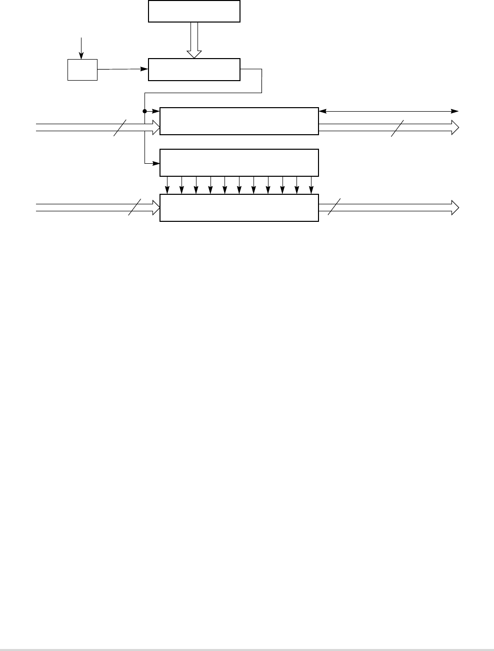
27-58 MCF5282 User’s Manual MOTOROLA
Digital Control Subsystem
Figure 27-42. QADC Clock Subsystem Functions
CAUTION
A change in the prescaler value while a conversion is in
progress is likely to corrupt the result. Therefore, any prescaler
write operation should be done only when both queues are in
the disabled modes.
To accommodate the wide range of the system clock frequency, QCLK is generated by a
programmable prescaler which divides the system clock. To allow the A/D conversion time
to be maximized across the spectrum of system clock frequencies, the QADC prescaler
permits the QCLK frequency to be software selectable. The frequency of QCLK is set with
the QPR field in QACR0.
27.8.9 Periodic/Interval Timer
The QADC periodic/interval timer can be used to generate trigger events at a
programmable interval, initiating execution of queue 1 and/or queue 2. The
periodic/interval timer stays reset under these conditions:
• Both queue 1 and queue 2 are programmed to any mode which does not use the
periodic/interval timer.
• System reset is asserted.
• Stop mode is enabled.
• Debug mode is enabled.
AT D C o nv e r t e r
State Machine
272829210 211 212 213 214 215 216 217
Periodic Timer/Interval Timer
Select
Binary Counter
Queue 1 and Queue 2 Timer
Mode Rate Selection
Input Sample Time
from CCW SAR
SAR Control
Periodic/Interval Trigger
Event for Q1 and Q2
Prescaler
System Clock
2
8
10
2
QPR[6:0]
Divide
by 2

MOTOROLA Chapter 27. Queued Analog-to-Digital Converter (QADC) 27-59
Digital Control Subsystem
NOTE
Interval timer single-scan mode does not start the
periodic/interval timer until the single-scan enable bit is set.
These conditions will cause a pulsed reset of the periodic/interval timer during use:
• A queue 1 operating mode change to a mode which uses the periodic/interval timer,
even if queue 2 is already using the timer
• A queue 2 operating mode change to a mode which uses the periodic/interval timer,
provided queue 1 is not in a mode which uses the periodic/interval timer
• Roll over of the timer
During stop mode, the periodic/interval timer is held in reset. Because stop mode causes
QACR1 and QACR2 to be reset to 0, a valid periodic or interval timer mode must be written
after leaving stop mode to release the timer from reset.
When QADC debug mode is entered and a periodic or interval timer mode is selected, the
timer counter is reset after the conversion in progress completes. When the periodic or
interval timer mode has been enabled (the timer is counting), but a trigger event has not
been issued, debug mode takes effect immediately, and the timer is held in reset. Removal
of the QADC debug condition restarts the counter from the beginning. Refer to
Section 27.3.1 for more information.
27.8.10 Conversion Command Word Table
The conversion command word (CCW) table is 64 half-word (128 byte) long RAM with 10
bits of each entry implemented. The CCW table is written by the user and is not modified
by the QADC. Each CCW requests the conversion of one analog channel to a digital result.
The CCW specifies the analog channel number, the input sample time, and whether the
queue is to pause after the current CCW. The 10 implemented bits of the CCW can be read
and written. The remaining six bits are unimplemented and read as 0s; write operations
have no effect. Each location in the CCW table corresponds to a location in the result word
table. When a conversion is completed for a CCW entry, the 10-bit result is written in the
corresponding result word entry.
The beginning of queue 1 is the first location in the CCW table. The first location of queue
2 is specified by the beginning of queue 2 pointer field (BQ2) in QACR2. To dedicate the
entire CCW table to queue 1, place queue 2 in disabled mode and write BQ2 to 64 or
greater. To dedicate the entire CCW table to queue 2, place queue 1 in disabled mode and
set BQ2 to the first location in the CCW table (CCW0).
Figure 27-43 illustrates the operation of the queue structure.
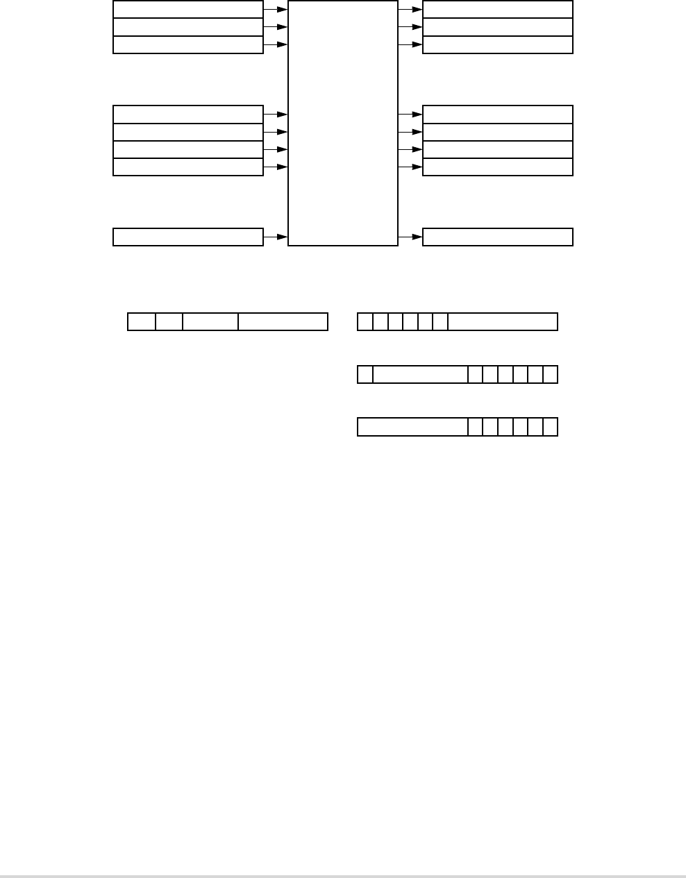
27-60 MCF5282 User’s Manual MOTOROLA
Digital Control Subsystem
Figure 27-43. QADC Conversion Queue Operation
To prepare the QADC for a scan sequence, write to the CCW table to specify the desired
channel conversions. The criteria for queue execution is established by selecting the queue
operating mode. The queue operating mode determines what type of trigger event starts
queue execution. A trigger event refers to any of the ways that cause the QADC to begin
executing the CCWs in a queue or subqueue. An external trigger is only one of the possible
trigger events.
A scan sequence may be initiated by:
• A software command
• Expiration of the periodic/interval timer
• An external trigger signal
• An external gated signal (queue 1 only)
The queue can be scanned in single pass or continuous fashion. When a single-scan mode
is selected, the scan must be engaged by setting the single-scan enable bit. When a
continuous-scan mode is selected, the queue remains active in the selected queue operating
mode after the QADC completes each queue scan sequence.
Beginning of Queue 1 00
Channel Select,
Sample, Hold,
A/D Conversion
Conversion Command
Result Word Table
Word (CCW) Table
00
End of Queue 1
Beginning of Queue 2
End of Queue 263 63
•
•
•
•
•
•
•
•
•
•
•
•
BYP
PIST CHAN
89 [7:6] [5:0]
P — Pause after Conversion
until Next Trigger
BYP — Bypass Buffer Amplifier
IST — Input Sample Time
CHAN — Channel Number and
End-of-Queue Code
10-bit Conversion Command
Word Format
0RESULT
[9:0]
10-bit Result, Readable in
Three 16-BIT Formats
00000
15 14 13 12 11 10
0
RESULT 00000
Right-Justified, Unsigned Result
Left-Justified, Unsigned Result
Left-Justified, Signed Result
0
RESULT 00000S
[5:0]
[5:0]
[15:6]
[15:6]

MOTOROLA Chapter 27. Queued Analog-to-Digital Converter (QADC) 27-61
Digital Control Subsystem
During queue execution, the QADC reads each CCW from the active queue and executes
conversions in three stages:
• Initial sample
• Final sample
• Resolution
During initial sample, a buffered version of the selected input channel is connected to the
sample capacitor at the input of the sample buffer amplifier.
During the final sample period, the sample buffer amplifier is bypassed, and the multiplexer
input charges the sample capacitor directly. Each CCW specifies a final input sample time
of 2, 4, 8, or 16 QCLK cycles. When an analog-to-digital conversion is complete, the result
is written to the corresponding location in the result word table. The QADC continues to
sequentially execute each CCW in the queue until the end of the queue is detected or a
pause bit is found in a CCW.
When the pause bit is set in the current CCW, the QADC stops execution of the queue until
a new trigger event occurs. The pause status flag bit is set, and an interrupt may optionally
be requested. After the trigger event occurs, the paused state ends, and the QADC continues
to execute each CCW in the queue until another pause is encountered or the end of the
queue is detected.
An end-of-queue condition occurs when:
• The CCW channel field is programmed with 63 to specify the end of the queue.
• The end-of-queue 1 is implied by the beginning of queue 2, which is specified by the
BQ2 field in QACR2.
• The physical end of the queue RAM space defines the end of either queue.
When any of the end-of-queue conditions is recognized, a queue completion flag is set, and
if enabled, an interrupt is requested. These situations prematurely terminate queue
execution:
• Queue 1 is higher in priority than queue 2. When a trigger event occurs on queue 1
during queue 2 execution, the execution of queue 2 is suspended by aborting the
execution of the CCW in progress, and queue 1 execution begins. When queue 1
execution is complete, queue 2 conversions restart with the first CCW entry in queue
2 or the first CCW of the queue 2 subqueue being executed when queue 2 was
suspended. Alternately, conversions can restart with the aborted queue 2 CCW entry.
The RESUME bit in QACR2 selects where queue 2 begins after suspension. By
choosing to re-execute all of the suspended queue 2 CCWs (RESUME = 0), all of
the samples are guaranteed to have been taken during the same scan pass. However,
a high trigger event rate for queue 1 can prevent completion of queue 2. If this
occurs, execution of queue 2 can begin with the aborted CCW entry (RESUME = 1).

27-62 MCF5282 User’s Manual MOTOROLA
Signal Connection Considerations
• Any conversion in progress for a queue is aborted when that queue’s operating mode
is changed to disabled. Putting a queue into the disabled mode does not power down
the converter.
• Changing a queue’s operating mode to another valid mode aborts any conversion in
progress. The queue restarts at its beginning once an appropriate trigger event
occurs.
• For low-power operation, the stop bit can be set to prepare the module for a loss of
clocks. The QADC aborts any conversion in progress when stop mode is entered.
• When the QADC debug bit is set and the CPU enters background debug mode, the
QADC freezes at the end of the conversion in progress. After leaving debug mode,
the QADC resumes queue execution beginning with the next CCW entry. Refer to
Section 27.3.1” for more information.
27.8.11 Result Word Table
The result word table is a 64 half-word (128 byte) long by 10-bit wide RAM. An entry is
written by the QADC after completing an analog conversion specified by the corresponding
CCW table entry. The result word table can be read or written, but in normal operation is
only read to obtain analog conversions from the QADC. Unimplemented bits read as 0s and
writes have no effect.
NOTE
Although the result RAM can be written, some write
operations, like bit manipulation, may not operate as expected
because the hardware cannot access a true 16-bit value.
While there is only one result word table, the half-word (16-bit) data can be accessed in
three different data formats:
• Right justified with 0s in the higher order unused bits
• Left justified with the most significant bit inverted to form a sign bit, and 0s in the
unused lower order bits
• Left justified with 0s in the lower order unused bits
The left justified, signed format corresponds to a half-scale, offset binary, two’s
complement data format. The address used to read the result table determines the data
alignment format. All write operations to the result word table are right justified.
27.9 Signal Connection Considerations
The QADC requires accurate, noise-free input signals for proper operation. This section
discusses the design of external circuitry to maximize QADC performance.
MOTOROLA Chapter 27. Queued Analog-to-Digital Converter (QADC) 27-63
Signal Connection Considerations
27.9.1 Analog Reference Signals
No A/D converter can be more accurate than its analog reference. Any noise in the
reference can result in at least that much error in a conversion. The reference for the QADC,
supplied by signals VRH and VRL, should be low-pass filtered from its source to obtain a
noise-free, clean signal. In many cases, simple capacitive bypassing may suffice. In
extreme cases, inductors or ferrite beads may be necessary if noise or RF energy is present.
External resistance may introduce error in this architecture under certain conditions. Any
series devices in the filter network should contain a minimum amount of DC resistance.
For accurate conversion results, the analog reference voltages must be within the limits
defined by VDDA and VSSA, as explained in this subsection.
27.9.2 Analog Power Signals
The analog supply signals (VDDA and VSSA) define the limits of the analog reference
voltages (VRH and VRL) and of the analog multiplexer inputs. Figure 27-44 is a diagram of
the analog input circuitry.
Figure 27-44. Equivalent Analog Input Circuitry
Because the sample amplifier is powered by VDDA and VSSA, it can accurately transfer
input signal levels up to but not exceeding VDDA and down to but not below VSSA. If the
input signal is outside of this range, the output from the sample amplifier is clipped.
In addition, VRH and VRL must be within the range defined by VDDA and VSSA. As long as
VRH is less than or equal to VDDA, and VRL is greater than or equal to VSSA, and the sample
amplifier has accurately transferred the input signal, resolution is ratiometric within the
limits defined by VRL and VRH. If VRH is greater than VDDA, the sample amplifier can
Sample
AMP
16 Channels Total
V
RL
VDDA VRH
S/H
Comparator
C
VSSA
27-64 MCF5282 User’s Manual MOTOROLA
Signal Connection Considerations
never transfer a full-scale value. If VRL is less than VSSA, the sample amplifier can never
transfer a 0 value.
Figure 27-45 shows the results of reference voltages outside the range defined by VDDA
and VSSA. At the top of the input signal range, VDDA is 10 mV lower than VRH. This results
in a maximum obtainable 10-bit conversion value 0x03fe. At the bottom of the signal range,
VSSA is 15 mV higher than VRL, resulting in a minimum obtainable 10-bit conversion value
of 0x0003.
Figure 27-45. Errors Resulting from Clipping
27.9.3 Conversion Timing Schemes
This section contains some conversion timing examples. Figure 27-46 shows the timing for
basic conversions where it is assumed that:
• Q1 begins with CCW0 and ends with CCW3.
• CCW0 has pause bit set.
• CCW1 does not have pause bit set.
• External trigger rising edge for Q1
• CCW4 = BQ2 and Q2 is disabled.
• Q1 RES shows relative result register updates.
0 .020 5.100 5.110
1
2
3
4
5
6
7
8
3FA
3FB
3FC
3FD
3FE
3FF
.010 .030 5.120 5.130
10-bit Result (Hexadecimal)
Inputs in Volts (VRH = 5.120 V, VRL = 0 V)
MOTOROLA Chapter 27. Queued Analog-to-Digital Converter (QADC) 27-65
Signal Connection Considerations
Recall that when QS = 0, both queues are disabled; when QS = 8, queue 1 is active and
queue 2 is idle; and when QS = 4; queue 1 is paused and queue 2 is disabled.
Figure 27-46. External Positive Edge Trigger Mode Timing with Pause
A time separator is provided between the triggers and the end of conversion (EOC). The
relationship to QCLK displayed is not guaranteed.
CWPQ1 and CWPQ2 typically lag CWP and only match CWP when the associated queue
is inactive. Another way to view CWPQ1 and CWPQ2 is that these registers update when
EOC triggers the write to the result register.
For the CCW with the pause bit set (CCW0), CWP does not increment until triggered. For
the CCW with the pause bit clear (CCW1), the CWP increments with the EOC.
The conversion results Q1 RESx show the result associated with CCWx, such that R0
represents the result associated with CCW0.
Figure 27-47 shows the timing for conversions in externally gated single-scan with same
assumptions in example 1 except:
• No pause bits set in any CCW
• Externally gated single scan mode for Q1
• Single scan enable bit (SSE1) is set.
When the gate closes and opens again, the conversions start with the first CCW in Q1.
R1
LAST
R0
CCW0 CCW1
CCW2CCW1
CONVERSION TIME
TIME BETWEEN
QCLK
TRIG1
EOC
QS
CWP
CWPQ1
Q1 RES
0
LAST
84 8
CCW0
TRIGGERS
= 14 QCLKS
CONVERSION TIME
= 14 QCLKS
27-66 MCF5282 User’s Manual MOTOROLA
Signal Connection Considerations
When the gate closes, the active conversion completes before the queue goes idle.
When Q1 completes, both the CF1 bit sets and the SSE bit clears.
In this mode, the PF1 bit sets to reflect that a gate closing occurred before the queue
completed.
Figure 27-48 shows the timing for conversions in externally gated continuous scan mode
with the same assumptions as in Figure 27-47.
At the end of Q1,the completion flag CF1 sets and the queue restarts. If the queue starts a
second time and completes, the trigger overrun flag TOR1 sets.
Figure 27-47. Gated Mode, Single Scan Timing
08 0 8 0
CCW3CCW2CCW1CCW0LAST CCW0 CCW1
R3R2R1R0LAST R0 R1
TRIG1 (GATE)
EOC
QS
CWP
CWPQ1
Q1 RES
SSE
CF1
PF1
LAST CCW0 CCW1 CCW1CCW0 CCW2 CCW3
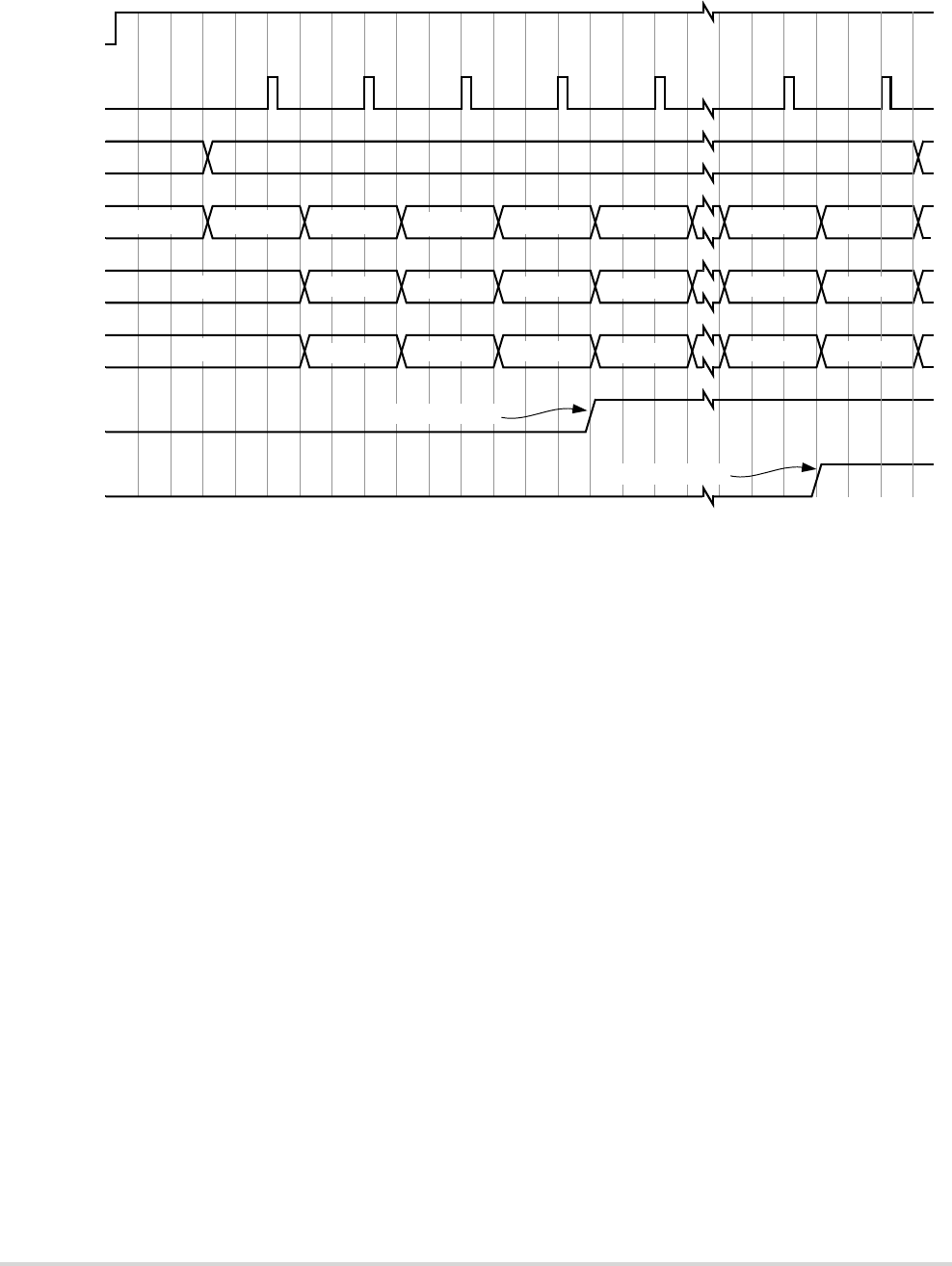
MOTOROLA Chapter 27. Queued Analog-to-Digital Converter (QADC) 27-67
Signal Connection Considerations
Figure 27-48. Gated Mode, Continuous Scan Timing
27.9.4 Analog Supply Filtering and Grounding
Two important factors influencing performance in analog integrated circuits are supply
filtering and grounding. Generally, digital circuits use bypass capacitors on every VDD/VSS
signal pair. This applies to analog subsystems and submodules also. Equally important as
bypassing is the distribution of power and ground.
Analog supplies should be isolated from digital supplies as much as possible. This necessity
stems from the higher performance requirements often associated with analog circuits.
Therefore, deriving an analog supply from a local digital supply is not recommended.
However, if for cost reasons digital and analog power are derived from a common regulator,
filtering of the analog power is recommended in addition to the bypassing of the supplies
already mentioned. For example, an RC low pass filter could be used to isolate the digital
and analog supplies when generated by a common regulator. If multiple high precision
analog circuits are locally employed (for example, two A/D converters), the analog supplies
should be isolated from each other as sharing supplies introduces the potential for
interference between analog circuits.
Grounding is the most important factor influencing analog circuit performance in mixed
signal systems (or in standalone analog systems). Close attention must be paid not to
introduce additional sources of noise into the analog circuitry. Common sources of noise
include ground loops, inductive coupling, and combining digital and analog grounds
together inappropriately.
EOC
QS
CWP
CSPQ1
Q1 RES
CF1
CCW0CCW3CCW0CCW3CCW2CCW1CCW0LAST
LAST
CCW0 CCW1 CCW2 CCW3
LAST
R0 R1 R2 R3 R2
CCW2
XX
08
Queue Restart
Queue Restart
TOR1
CCW3
R3
TRIG1 (GATE)
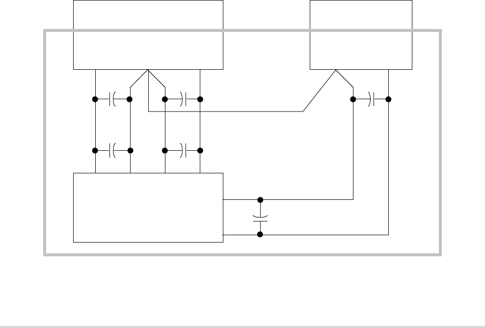
27-68 MCF5282 User’s Manual MOTOROLA
Signal Connection Considerations
The problem of how and when to combine digital and analog grounds arises from the large
transients which the digital ground must handle. If the digital ground is not able to handle
the large transients, the associated current can return to ground through the analog ground.
It is this excess current overflowing into the analog ground which causes performance
degradation by developing a differential voltage between the true analog ground and the
microcontroller’s ground pins. The end result is that the ground observed by the analog
circuit is no longer true ground and thus skews converter performance.
Two similar approaches to improving or eliminating the problems associated with
grounding excess transient currents involve star-point ground systems. One approach is to
star-point the different grounds at the power supply origin, thus keeping the ground
isolated. Refer to Figure 27-49.
Another approach is to star-point the different grounds near the analog ground signal on the
microcontroller by using small traces for connecting the non-analog grounds to the analog
ground. The small traces are meant only to accommodate dc differences, not ac transients.
NOTE
This star-point scheme still requires adequate grounding for
digital and analog subsystems in addition to the star-point
ground.
Figure 27-49. Star-Ground at the Point of Power Supply Origin
Other suggestions for PCB layout in which the QADC is employed include:
QADC
VRH
VRL
VSSA
VDDA
VDD
VSS
Analog Power Supply
+5 V
+5 V AGND
Digital Power Supply
+5 V
PGND
PCB
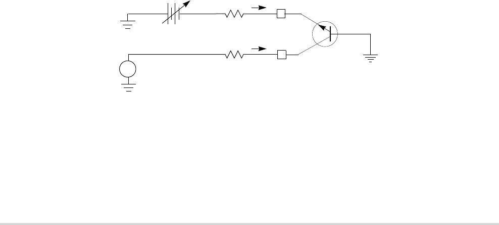
MOTOROLA Chapter 27. Queued Analog-to-Digital Converter (QADC) 27-69
Signal Connection Considerations
• Analog ground must be low impedance to all analog ground points in the circuit.
• Bypass capacitors should be as close to the power pins as possible.
• The analog ground should be isolated from the digital ground. This can be done by
cutting a separate ground plane for the analog ground.
• Non-minimum traces should be utilized for connecting bypass capacitors and filters
to their corresponding ground/power points.
• Minimum distance for trace runs when possible.
27.9.5 Accommodating Positive/Negative Stress Conditions
Positive or negative stress refers to conditions which exceed nominally defined operating
limits. Examples include applying a voltage exceeding the normal limit on an input (for
example, voltages outside of the suggested supply/reference ranges) or causing currents
into or out of the pin which exceed normal limits. QADC specific considerations are
voltages greater than VDDA or less than VSSA applied to an analog input which cause
excessive currents into or out of the input. Refer to MCF5282 Electrical Characteristics for
more information on exact magnitudes.
Either stress conditions can potentially disrupt conversion results on neighboring inputs.
Parasitic devices, associated with CMOS processes, can cause an immediate disruptive
influence on neighboring pins. Common examples of parasitic devices are diodes to
substrate and bipolar devices with the base terminal tied to substrate (VSS/VSSA ground).
Under stress conditions, current injected on an adjacent signal can cause errors on the
selected channel by developing a voltage drop across the selected channel’s impedances.
Figure 27-50 shows an active parasitic bipolar NPN transistor when an input signal is
subjected to negative stress conditions. Figure 27-51 shows positive stress conditions can
activate a similar PNP transistor.
Figure 27-50. Input Signal Subjected to Negative Stress
RSTRESS
RSELECTED
Adjacent
10 kΩ
Signal Under
Parasitic
Iinjn
IIN
+
Stress
VSTRESS
Device
Signal
VIN
ANn
ANn+1
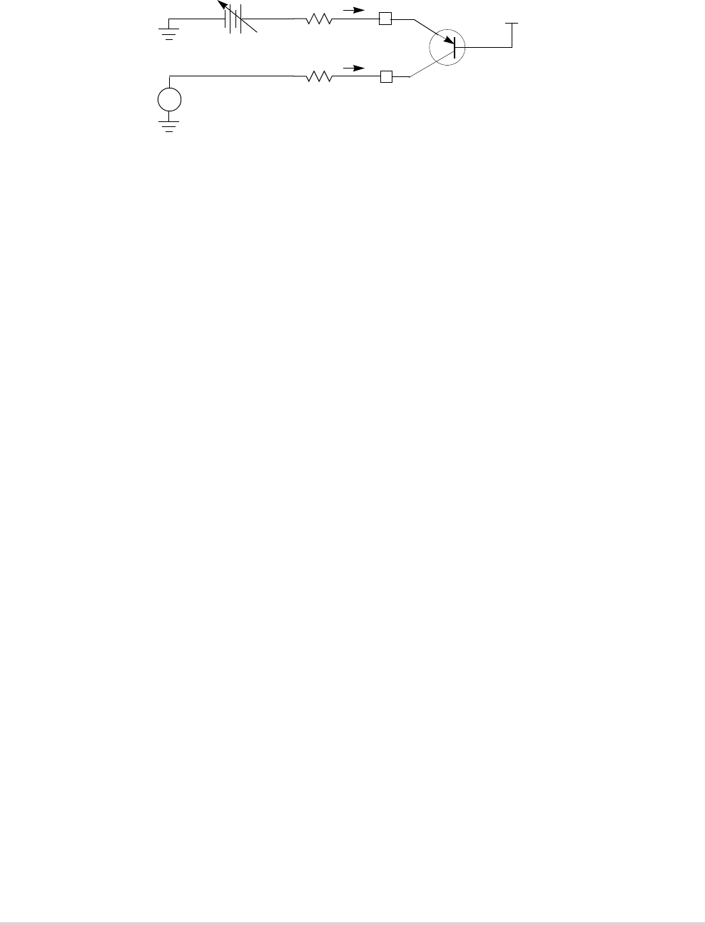
27-70 MCF5282 User’s Manual MOTOROLA
Signal Connection Considerations
Figure 27-51. Input Signal Subjected to Positive Stress
The current into the signal (IINJN or IINJP) under negative or positive stress is determined by
these equations:
Where:
VStress = Adjustable voltage source
VEB = Parasitic PNP emitter/base voltage
VBE= Parasitic NPN base/emitter voltage
RStress= Source impedance (10 kΩ resistor in Figure 27-50 and Figure 27-51 on stressed
channel)
RSelected = Source impedance on channel selected for conversion
The current into (IIn) the neighboring pin is determined by the KN (current coupling ratio)
of the parasitic bipolar transistor (KN ‹‹ 1). The IIn can be expressed by this equation:
IIn = – KN * IINJ
Where:
IINJ is either IINJN or IINJP
.
A method for minimizing the impact of stress conditions on the QADC is to strategically
allocate QADC inputs so that the lower accuracy inputs are adjacent to the inputs most
likely to see stress conditions.
Also, suitable source impedances should be selected to meet design goals and minimize the
effect of stress conditions.
RSTRESS
RSELECTED
Adjacent
10 kΩ
Signal Under
Parasitic
IinjP
IIN
+
Stress
VSTRESS
Device
Signal
VIN
VDDA
ANn
ANn+1
IINJN
VStress VBE
–()–
RStress
---------------------------------------------=
IINJP
VStress VEB
–V
DDA
–
RStress
-------------------------------------------------------------=

MOTOROLA Chapter 27. Queued Analog-to-Digital Converter (QADC) 27-71
Signal Connection Considerations
27.9.6 Analog Input Considerations
The source impedance of the analog signal to be measured and any intermediate filtering
should be considered whether external multiplexing is used or not. Figure 27-52 shows the
connection of eight typical analog signal sources to one QADC analog input signal through
a separate multiplexer chip. Also, an example of an analog signal source connected directly
to a QADC analog input channel is displayed.
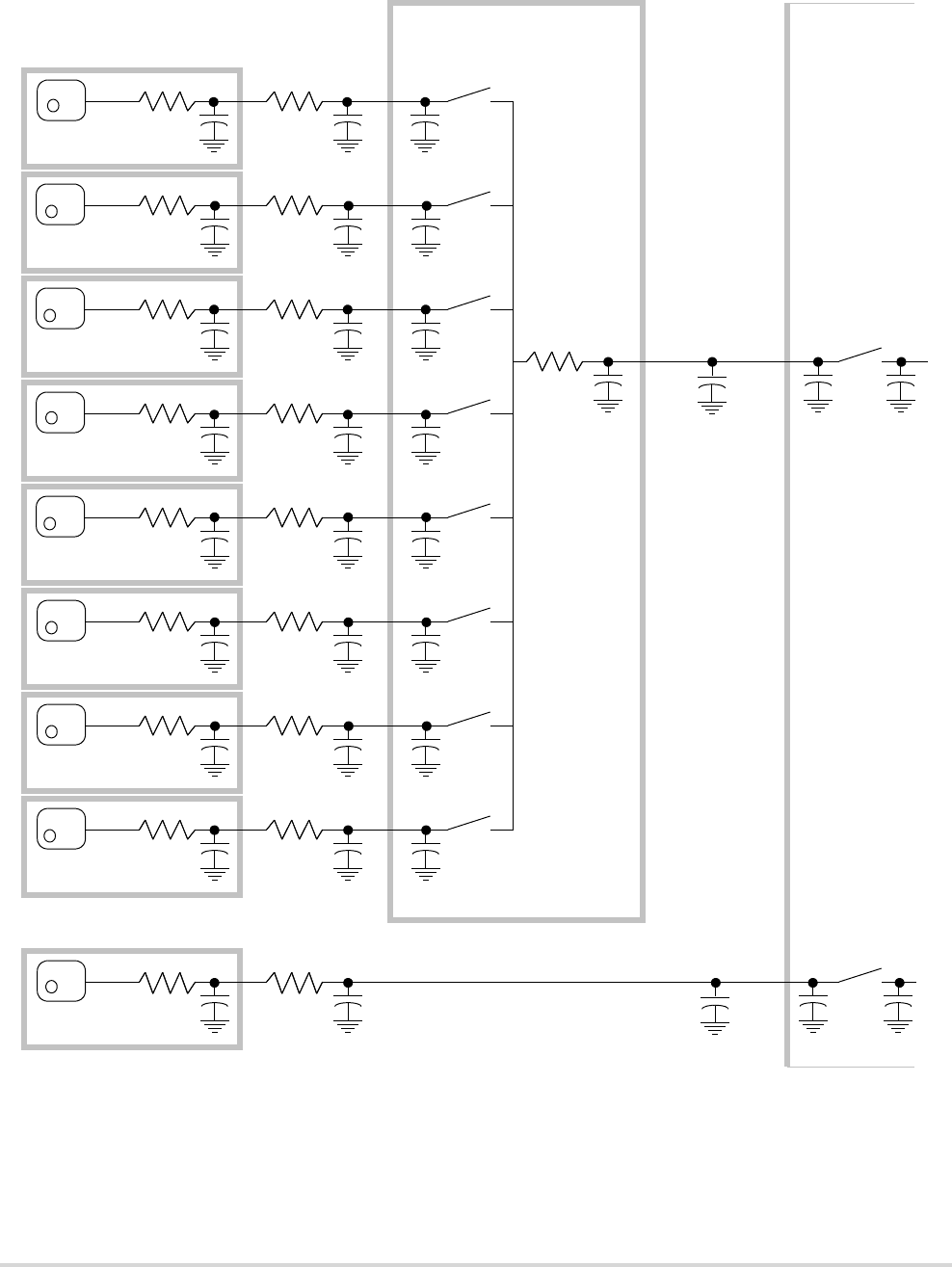
27-72 MCF5282 User’s Manual MOTOROLA
Signal Connection Considerations
Figure 27-52. External Multiplexing of Analog Signal Sources
CPCSAMP
CPCSAMP
CIn = CP + CSAMP
RMUXOUT
RSource2
Analog Signal Source
Filtering and
Interconnect
Typical MUX Chip
Interconnect QADC
~
CFilter
CSource
RFilter2
CMUXIN
0.01 µF1
CMUXOUT
(MC54HC4051, MC74HC4051,
MC54HC4052, MC74HC4052,
MC54HC4053, etc.)
RSource2
CFilter
CSource
RFilter2
CMUXIN
0.01 µF1
RSource2
CFilter
CSource
RFilter2
CMUXIN
0.01 µF1
RSource2
CFilter
CSource
RFilter2
CMUXIN
0.01 µF1
RSource2
CFilter
CSource
RFilter2
CMUXIN
0.01µF1
RSource2
CFilter
CSource
RFilter2
CMUXIN
0.01 µF1
RSource2
CFilter
CSource
RFilter2
CMUXIN
0.01 µF1
RSource2
CFilter
CSource
RFilter2
CMUXIN
0.01 µF1
CFilter
RFilter2
0.01 µF1
1. Typical Value
2. RFilter, Typically 10 kΩ–20 kΩ
Notes:
RSource2
CSource
CPCB
CPCB
~
~
~
~
~
~
~
~
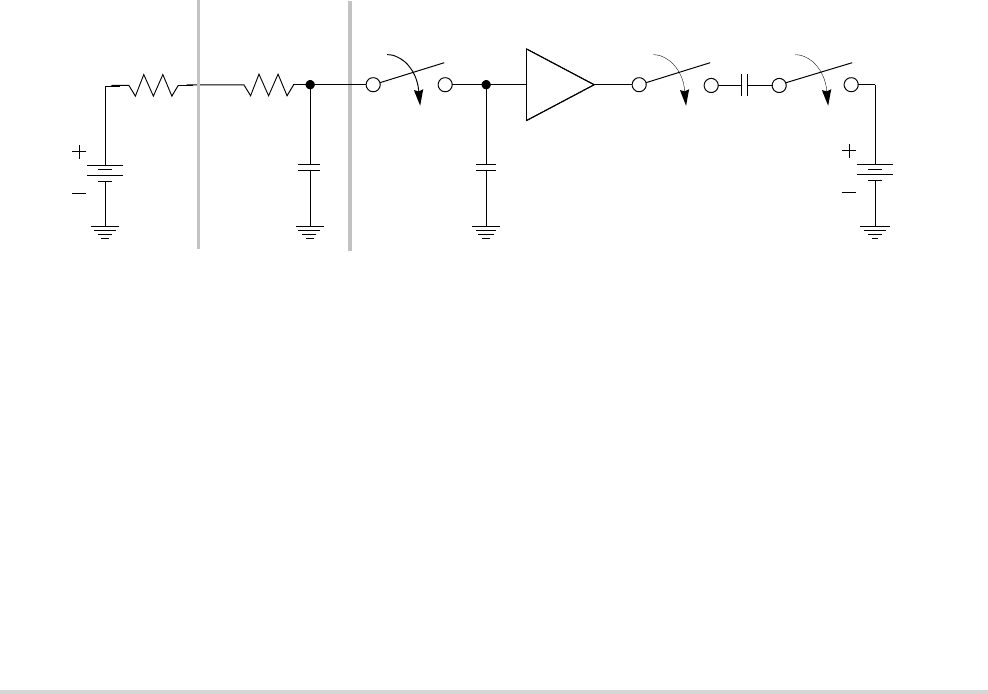
MOTOROLA Chapter 27. Queued Analog-to-Digital Converter (QADC) 27-73
Signal Connection Considerations
27.9.7 Analog Input Pins
Analog inputs should have low AC impedance at the pins. Low AC impedance can be
realized by placing a capacitor with good high frequency characteristics at the input signal
of the device. Ideally, that capacitor should be as large as possible (within the practical
range of capacitors that still have good high-frequency characteristics). This capacitor has
two effects:
• It helps attenuate any noise that may exist on the input.
• It sources charge during the sample period when the analog signal source is a
high-impedance source.
Series resistance can be used with the capacitor on an input signal to implement a simple
RC filter. The maximum level of filtering at the input pins is application dependent and is
based on the bandpass characteristics required to accurately track the dynamic
characteristics of an input. Simple RC filtering at the pin may be limited by the source
impedance of the transducer or circuit supplying the analog signal to be measured. (See
Section 27.9.7.2.”) In some cases, the size of the capacitor at the pin may be very small.
Figure 27-53 is a simplified model of an input channel. Refer to this model in the following
discussion of the interaction between the external circuitry and the circuitry inside the
QADC.
Figure 27-53. Electrical Model of an A/D Input Signal
In Figure 27-53, RF, RSRC, and CF comprise the external filter circuit. CP is the internal
parasitic capacitor. CSAMP is the capacitor array used to sample and hold the input voltage.
VI is an internal voltage source used to provide charge to CSAMP during sample phase.
The following paragraphs provide a simplified description of the interaction between the
QADC and the user's external circuitry. This circuitry is assumed to be a simple RC
low-pass filter passing a signal from a source to the QADC input signal. These paragraphs
make the following assumptions:
S1
AMP
RF
S3
CSAMP
VICP
CF
VSRC
Internal Circuit ModelExternal Filter
VSRC = Source Voltage = Internal Parasitic Capacitance
RF
CF
CP
CSAMP = Sample Capacitor
V
I
= Filter Impedance
= Filter Capacitor
= Internal Voltage Source During Sample and Hold
Source
RSRC
RSRC = Source Impedance
S2

27-74 MCF5282 User’s Manual MOTOROLA
Signal Connection Considerations
• The external capacitor is perfect (no leakage, no significant dielectric absorption
characteristics, etc.).
• All parasitic capacitance associated with the input signal is included in the value of
the external capacitor.
• Inductance is ignored.
• The “on” resistance of the internal switches is 0 ohms and the “off” resistance is
infinite.
27.9.7.1 Settling Time for the External Circuit
The values for RSRC, RF, and CF in the user's external circuitry determine the length of time
required to charge CF to the source voltage level (VSRC). At time t = 0, VSRC changes in
Figure 27-53 while S1 is open, disconnecting the internal circuitry from the external
circuitry. Assume that the initial voltage across CF is 0. As CF charges, the voltage across
it is determined by the equation, where t is the total charge time:
As t approaches infinity, VCF will equal VSRC. (This assumes no internal leakage.) With
10-bit resolution, 1/2 of a count is equal to 1/2048 full-scale value. Assuming worst case
(VSRC = full scale), Table 27-24 shows the required time for CF to charge to within 1/2 of
a count of the actual source voltage during 10-bit conversions. Table 27-24 is based on the
RC network in Figure 27-53.
NOTE
The following times are completely independent of the A/D
converter architecture (assuming the QADC is not affecting the
charging).
The external circuit described in Table 27-24 is a low-pass filter. Measurements of an AC
component of the external signal must take the characteristics of this filter into account.
Table 27-24. External Circuit Settling Time to 1/2 LSB
Filter Capacitor (CF)
Source Resistance (RF + RSRC)
100 Ω1 kΩ10 kΩ100 kΩ
1 µF 760 µs 7.6 ms 76 ms 760 ms
0.1 µF 76 µs 760 µs 7.6 ms 76 ms
0.01 µF7.6 µs 76 µs 760 µs7.6 ms
0.001 µF 760 ns 7.6 µs 76 µs 760 µs
100 pF 76 ns 760 ns 7.6 µs 76 µs
VCF = VSRC (1 –e–t/(RF + RSRC) CF)

MOTOROLA Chapter 27. Queued Analog-to-Digital Converter (QADC) 27-75
Interrupts
27.9.7.2 Error Resulting from Leakage
A series resistor limits the current to a signal; therefore, input leakage acting through a large
source impedance can degrade A/D accuracy. The maximum input leakage current is
specified in MCF5282 Electrical Specifications. Input leakage is greater at higher operating
temperatures. In the temperature range from 125°C to 50°C, the leakage current is halved
for every 8°C to 12°C reduction in temperature.
Assuming VRH–VRL = 5.12 V, 1 count (with 10-bit resolution) corresponds to 5 mV of
input voltage. A typical input leakage of 200 nA acting through 10 kΩ of external series
resistance results in an error of 0.4 count (2.0 mV). If the source impedance is 100 kΩ and
a typical leakage of 100 nA is present, an error of 2 counts (10 mV) is introduced.
In addition to internal junction leakage, external leakage (for example, if external clamping
diodes are used) and charge sharing effects with internal capacitors also contribute to the
total leakage current. Table 27-25 illustrates the effect of different levels of total leakage on
accuracy for different values of source impedance. The error is listed in terms of 10-bit
counts.
CAUTION
Leakage below 200 nA is obtainable only within a limited
temperature range.
27.10 Interrupts
The four interrupt lines are outputs of the module and have no priority or arbitration within
the module.
27.10.1 Interrupt Operation
QADC inputs can be monitored by polling or by using interrupts. When interrupts are not
needed, the completion flag and the pause flag for each queue can be monitored in the status
register (QASR0). In other words, flag bits can be polled to determine when new results are
available.
Table 27-26 shows the status flag and interrupt enable bits which correspond to queue 1 and
queue 2 activity.
Table 27-25. Error Resulting from Input Leakage (IOff)
Source Impedance
Leakage Value (10-Bit Conversions)
100 nA 200 nA 500 nA 1000 nA
1 kΩ— — 0.1 counts 0.2 counts
10 kΩ0.2 counts 0.4 counts 1 counts 2 counts
100 kΩ2 counts 4 count 10 counts 20 counts

27-76 MCF5282 User’s Manual MOTOROLA
Interrupts
If interrupts are enabled for an event, the QADC requests interrupt service when the event
occurs. Using interrupts does not require continuously polling the status flags to see if an
event has taken place; however, status flags must be cleared after an interrupt is serviced,
in order to remove the interrupt request
In both polled and interrupt-driven operating modes, status flags must be re-enabled after
an event occurs. Flags are re-enabled by clearing the appropriate QASR0 bits in a particular
sequence. QASR0 must first be read, then 0s must be written to the flags that are to be
cleared. If a new event occurs between the time that the register is read and the time that it
is written, the associated flag is not cleared.
27.10.2 Interrupt Sources
The QADC includes four sources of interrupt requests, each of which is separately enabled.
Each time the result is written for the last conversion command word (CCW) in a queue,
the completion flag for the corresponding queue is set, and when enabled, an interrupt is
requested. In the same way, each time the result is written for a CCW with the pause bit set,
the queue pause flag is set, and when enabled, an interrupt is requested. Refer to
Table 27-26.
The pause and complete interrupts for queue 1 and queue 2 have separate interrupt vector
levels, so that each source can be separately serviced.
Table 27-26. QADC Status Flags and Interrupt Sources
Queue Queue Activity Status
Flag
Interrupt
Enable Bit
Queue 1 Result written for last CCW in queue 1 CF1 CIE1
Result written for a CCW with pause bit set in queue 1 PF1 PIE1
Queue 2 Result written for last CCW in queue 2 CF2 CIE2
Result written for a CCW with pause bit set in queue 2 PF2 PIE2

MOTOROLA Chapter 28. Reset Controller Module 28-1
Chapter 28
Reset Controller Module
The reset controller is provided to determine the cause of reset, assert the appropriate reset
signals to the system, and then to keep a history of what caused the reset. The Low Voltage
Detection module, which generates low-voltage detect (LVD) interrupts and resets, is
implemented within the reset controller module.
28.1 Features
Module features include:
• Seven sources of reset:
— External
— Power-on reset (POR)
— Watchdog timer
— Phase locked-loop (PLL) loss of lock
— PLL loss of clock
— Software
—LVD reset
• Software-assertable RSTO pin independent of chip reset state
• Software-readable status flags indicating the cause of the last reset
• LVD control and status bits for setup and use of LVD reset or interrupt
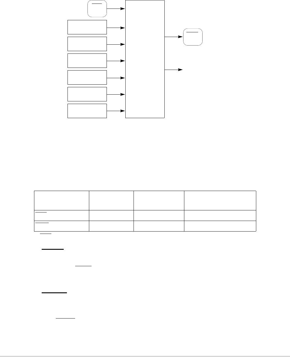
28-2 MCF5282 User’s Manual MOTOROLA
Block Diagram
28.2 Block Diagram
Figure 28-1 illustrates the reset controller and is explained in the following sections.
Figure 28-1. Reset Controller Block Diagram
28.3 Signals
Table 28-1 provides a summary of the reset controller signal properties. The signals are
described in the following paragraphs.
28.3.1 RSTI
Asserting the external RSTI for at least four rising CLKOUT edges causes the external reset
request to be recognized and latched.
28.3.2 RSTO
This active-low output signal is driven low when the internal reset controller module resets
the chip. When RSTO is active, the user can drive override options on the data bus.
Table 28-1. Reset Controller Signal Properties
Name Direction Input
Hysteresis
Input
Synchronization
RSTI IY Y
1
1RSTI is always synchronized except when in low-power stop mode.
RSTO O— —
Power-On
Reset
Watchdog
Timer Timeout
PLL
Loss of Clock
PLL
Loss of Lock
Software
Reset
LVD
Detect
RSTI
Pin
Reset
Controller
RSTO
Pin
To Internal Resets
MOTOROLA Chapter 28. Reset Controller Module 28-3
Memory Map and Registers
28.4 Memory Map and Registers
The reset controller programming model consists of these registers:
• Reset control register (RCR), which selects reset controller functions
• Reset status register (RSR), which reflects the state of the last reset source
See Table 28-2 for the memory map and the following paragraphs for a description of the
registers.
28.4.1 Reset Control Register (RCR)
The RCR allows software control for requesting a reset, for independently asserting the
external RSTO pin, and for controlling low-voltage detect (LVD) functions.
Table 28-2. Reset Controller Memory Map
IPSBAR Offset Bits 7:0 Access 1
1S/U = supervisor or user mode access.
0x11_0000 RCR S/U
0x11_0001 RSR S/U
0x11_0002 Reserved2—
0x11_0003 Reserved 2
2Writes to reserved address locations have no effect and reads return 0s.
—
7654 0
Field SOFTRST FRCRSTOUT — LVDF LVDIE LVDRE — LVDE
Reset 0000_0101
R/W R/W
Address IPSBAR + 0x11_0000
Figure 28-2. Reset Control Register (RCR)
Table 28-3. RCR Field Descriptions
Bit(s) Name Description
7 SOFTRST Allows software to request a reset. The reset caused by setting this bit clears this bit.
1 Software reset request
0 No software reset request
6 FRCRSTOUT Allows software to assert or negate the external RSTO pin.
1 Assert RSTO pin
0 Negate RSTO pin
CAUTION: External logic driving reset configuration data during reset needs to be considered
when asserting the RSTO pin when setting FRCRSTOUT.
5 — Reserved, should be cleared.

28-4 MCF5282 User’s Manual MOTOROLA
Memory Map and Registers
28.4.2 Reset Status Register (RSR)
The RSR contains a status bit for every reset source. When reset is entered, the cause of the
reset condition is latched along with a value of 0 for the other reset sources that were not
pending at the time of the reset condition. These values are then reflected in RSR. One or
more status bits may be set at the same time. The cause of any subsequent reset is also
recorded in the register, overwriting status from the previous reset condition.
RSR can be read at any time. Writing to RSR has no effect.
4 LVDF LVD flag. Indicates the low-voltage detect status if LVDE is set. Write a 1 to clear the LVDF bit.
1 Low voltage has been detected
0 Low voltage has not been detected
NOTE: The setting of this flag causes an LVD interrupt if LVDE and LVDIE bits are set and
LVDRE is cleared when the supply voltage VDD drops below VDD (minimum). The vector for
this interrupt is shared with INT0 of the EPORT module. Interrupt arbitration in the interrupt
service routine is necessary if both of these interrupts are enabled. Also, LVDF is not cleared
at reset, however it will always initialize to a zero since the part will not come out of reset while
in a low-power state (LVDE/LVDRE bits are enabled out of reset).
3 LVDIE LVD interrupt enable. Controls the LVD interrupt if LVDE is set. This bit has no effect if the
LVDE bit is a logic 0.
1 LVD interrupt enabled
0 LVD interrupt disabled
2 LVDRE LVD reset enable. Controls the LVD reset if LVDE is set. This bit has no effect if the LVDE bit
is a logic 0. LVD reset has priority over LVD interrupt, if both are enabled.
1 LVD reset enabled
0LVD reset disabled
1 — Reserved, should be cleared.
0 LVDE Controls whether the LVD is enabled.
1 LVD is enabled
0 LVD is disabled
76543210
Field — LVD SOFT WDR POR EXT LOC LOL
Reset Reset Dependent
R/W R
Address IPSBAR + 0x11_0001
Figure 28-3. Reset Status Register (RSR)
Table 28-3. RCR Field Descriptions (continued)
Bit(s) Name Description

MOTOROLA Chapter 28. Reset Controller Module 28-5
Memory Map and Registers
Table 28-4. RSR Field Descriptions
Bit(s) Name Description
7 — Reserved, should be cleared.
6 LVD Low voltage detect. Indicates that the last reset state was caused by an LVD reset.
1 Last reset state was caused by an LVD reset
0 Last reset state was not caused by an LVD reset
5 SOFT Software reset flag. Indicates that the last reset was caused by software.
1 Last reset caused by software
0 Last reset not caused by software
4 WDR Watchdog timer reset flag. Indicates that the last reset was caused by a watchdog timer timeout.
1 Last reset caused by watchdog timer timeout
0 Last reset not caused by watchdog timer timeout
3 POR Power-on reset flag. Indicates that the last reset was caused by a power-on reset.
1 Last reset caused by power-on reset
0 Last reset not caused by power-on reset
2 EXT External reset flag. Indicates that the last reset was caused by an external device asserting the
external RSTI pin.
1 Last reset state caused by external reset
0 Last reset not caused by external reset
1 LOC Loss-of-clock reset flag. Indicates that the last reset state was caused by a PLL loss of clock.
1 Last reset caused by loss of clock
0 Last reset not caused by loss of clock
0 LOL Loss-of-lock reset flag. Indicates that the last reset state was caused by a PLL loss of lock.
1 Last reset caused by a loss of lock
0 Last reset not caused by loss of lock

28-6 MCF5282 User’s Manual MOTOROLA
Functional Description
28.5 Functional Description
28.5.1 Reset Sources
Table 28-5 defines the sources of reset and the signals driven by the reset controller.
To protect data integrity, a synchronous reset source is not acted upon by the reset control
logic until the end of the current bus cycle. Reset is then asserted on the next rising edge of
the system clock after the cycle is terminated. Whenever the reset control logic must
synchronize reset to the end of the bus cycle, the internal bus monitor is automatically
enabled regardless of the BME bit state in the chip configuration register (CCR). Then, if
the current bus cycle is not terminated normally the bus monitor terminates the cycle based
on the length of time programmed in the BMT field of the CCR.
Internal byte, word, or longword writes are guaranteed to complete without data corruption
when a synchronous reset occurs. External writes, including longword writes to 16-bit
ports, are also guaranteed to complete.
Asynchronous reset sources usually indicate a catastrophic failure. Therefore, the reset
control logic does not wait for the current bus cycle to complete. Reset is asserted
immediately to the system.
28.5.1.1 Power-On Reset
At power up, the reset controller asserts RSTO. RSTO continues to be asserted until VDD
has reached a minimum acceptable level and, if PLL clock mode is selected, until the PLL
achieves phase lock. Then after approximately another 512 cycles, RSTO is negated and
the part begins operation.
Table 28-5. Reset Source Summary
Source Type
Power on Asynchronous
External RSTI pin (not stop mode) Synchronous
External RSTI pin (during stop mode) Asynchronous
Watchdog timer Synchronous
Loss of clock Asynchronous
Loss of lock Asynchronous
Software Synchronous
LVD reset Asynchronous

MOTOROLA Chapter 28. Reset Controller Module 28-7
Functional Description
28.5.1.2 External Reset
Asserting the external RSTI for at least four rising CLKOUT edges causes the external reset
request to be recognized and latched. The bus monitor is enabled and the current bus cycle
is completed. The reset controller asserts RSTO for approximately 512 cycles after RSTI is
negated and the PLL has acquired lock. The part then exits reset and begins operation.
In low-power stop mode, the system clocks are stopped. Asserting the external RSTI in stop
mode causes an external reset to be recognized.
28.5.1.3 Watchdog Timer Reset
A watchdog timer timeout causes timer reset request to be recognized and latched. The bus
monitor is enabled and the current bus cycle is completed. If the RSTI is negated and the
PLL has acquired lock, the reset controller asserts RSTO for approximately 512 cycles.
Then the part exits reset and begins operation.
28.5.1.4 Loss-of-Clock Reset
This reset condition occurs in PLL clock mode when the LOCRE bit in the SYNCR is set
and either the PLL reference or the PLL itself fails. The reset controller asserts RSTO for
approximately 512 cycles after the PLL has acquired lock. The part then exits reset and
begins operation.
28.5.1.5 Loss-of-Lock Reset
This reset condition occurs in PLL clock mode when the LOLRE bit in the SYNCR is set
and the PLL loses lock. The reset controller asserts RSTO for approximately 512 cycles
after the PLL has acquired lock. The part then exits reset and resumes operation.
28.5.1.6 Software Reset
A software reset occurs when the SOFTRST bit is set. If the RSTI is negated and the PLL
has acquired lock, the reset controller asserts RSTO for approximately 512 cycles. Then the
part exits reset and resumes operation.
28.5.1.7 LVD Reset
The LVD reset will occur when the supply input voltage, VDD, drops below VLVD
(minimum).

28-8 MCF5282 User’s Manual MOTOROLA
Functional Description
28.5.2 Reset Control Flow
The reset logic control flow is shown in Figure 28-4. In this figure, the control state boxes
have been numbered, and these numbers are referred to (within parentheses) in the flow
description that follows. All cycle counts given are approximate.
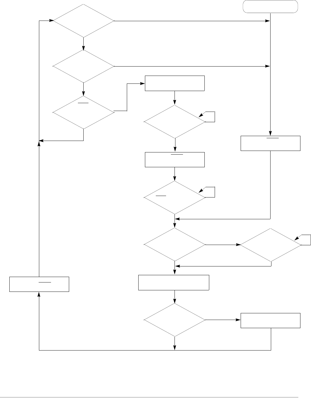
MOTOROLA Chapter 28. Reset Controller Module 28-9
Functional Description
Figure 28-4. Reset Control Flow
RSTI
PIN OR WD TIMEOUT
OR SW RESET?
LOSS OF CLOCK?
LOSS OF LOCK?
RSTI NEGATED?
PLL MODE?
BUS CYCLE
COMPLETE?
RCON ASSERTED?
PLL LOCKED?
ENABLE BUS MONITOR
ASSERT RSTO AND
LATCH RESET STATUS
WAIT 512 CLKOUT CYCLES
LATCH CONFIGURATION
NEGATE RSTO
POR OR LVD
ASSERT RSTO AND
LATCH RESET STATUS
N
N
N
Y
Y
Y
1
2
3
N
N
N
0
5
6
7
8
9
10
11
Y
Y
N
N
Y
Y
12
4
9A
11A
Y

28-10 MCF5282 User’s Manual MOTOROLA
Functional Description
28.5.2.1 Synchronous Reset Requests
In this discussion, the reference in parentheses refer to the state numbers in Figure 28-4. All
cycle counts given are approximate.
If the external RSTI signal is asserted by an external device for at least four rising
CLKOUT edges (3), if the watchdog timer times out, or if software requests a reset, the
reset control logic latches the reset request internally and enables the bus monitor (5). When
the current bus cycle is completed (6), RSTO is asserted (7). The reset control logic waits
until the RSTI signal is negated (8) and for the PLL to attain lock (9, 9A) before waiting
512 CLKOUT cycles (1). The reset control logic may latch the configuration according to
the RCON signal level (11, 11A) before negating RSTO (12).
If the external RSTI signal is asserted by an external device for at least four rising
CLKOUT edges during the 512 count (10) or during the wait for PLL lock (9A), the reset
flow switches to (8) and waits for the RSTI signal to be negated before continuing.
28.5.2.2 Internal Reset Request
If reset is asserted by an asynchronous internal reset source, such as loss of clock (1) or loss
of lock (2), the reset control logic asserts RSTO (4). The reset control logic waits for the
PLL to attain lock (9, 9A) before waiting 512 CLKOUT cycles (1). Then the reset control
logic may latch the configuration according to the RCON pin level (11, 11A) before
negating RSTO (12).
If loss of lock occurs during the 512 count (10), the reset flow switches to (9A) and waits
for the PLL to lock before continuing.
28.5.2.3 Power-On Reset/Low-Voltage Detect Reset
When the reset sequence is initiated by power-on reset (0), the same reset sequence is
followed as for the other asynchronous reset sources.
28.5.3 Concurrent Resets
This section describes the concurrent resets. As in the previous discussion references in
parentheses refer to the state numbers in Figure 28-4.
28.5.3.1 Reset Flow
If a power-on reset or low-voltage detect condition is detected during any reset sequence,
the reset sequence starts immediately (0).
If the external RSTI pin is asserted for at least four rising CLKOUT edges while waiting
for PLL lock or the 512 cycles, the external reset is recognized. Reset processing switches
to wait for the external RSTI pin to negate (8).

MOTOROLA Chapter 28. Reset Controller Module 28-11
Functional Description
If a loss-of-clock or loss-of-lock condition is detected while waiting for the current bus
cycle to complete (5, 6) for an external reset request, the cycle is terminated. The reset
status bits are latched (7) and reset processing waits for the external RSTI pin to negate (8).
If a loss-of-clock or loss-of-lock condition is detected during the 512 cycle wait, the reset
sequence continues after a PLL lock (9, 9A).
28.5.3.2 Reset Status Flags
For a POR reset, the POR and LVD bits in the RSR are set, and the SOFT, WDR, EXT,
LOC, and LOL bits are cleared even if another type of reset condition is detected during the
reset sequence for the POR.
If a loss-of-clock or loss-of-lock condition is detected while waiting for the current bus
cycle to complete (5, 6) for an external reset request, the EXT, SOFT, and/or WDR bits
along with the LOC and/or LOL bits are set.
If the RSR bits are latched (7) during the EXT, SOFT, and/or WDR reset sequence with no
other reset conditions detected, only the EXT, SOFT, and/or WDR bits are set.
If the RSR bits are latched (4) during the internal reset sequence with the RSTI pin not
asserted and no SOFT or WDR event, then the LOC and/or LOL bits are the only bits set.
For a LVD reset, the LVD bit in the RSR is set, and the SOFT, WDR, EXT, LOC, and LOL
bits are cleared to 0 even if another type of reset condition is detected during the reset
sequence for LVD.

28-12 MCF5282 User’s Manual MOTOROLA
Functional Description
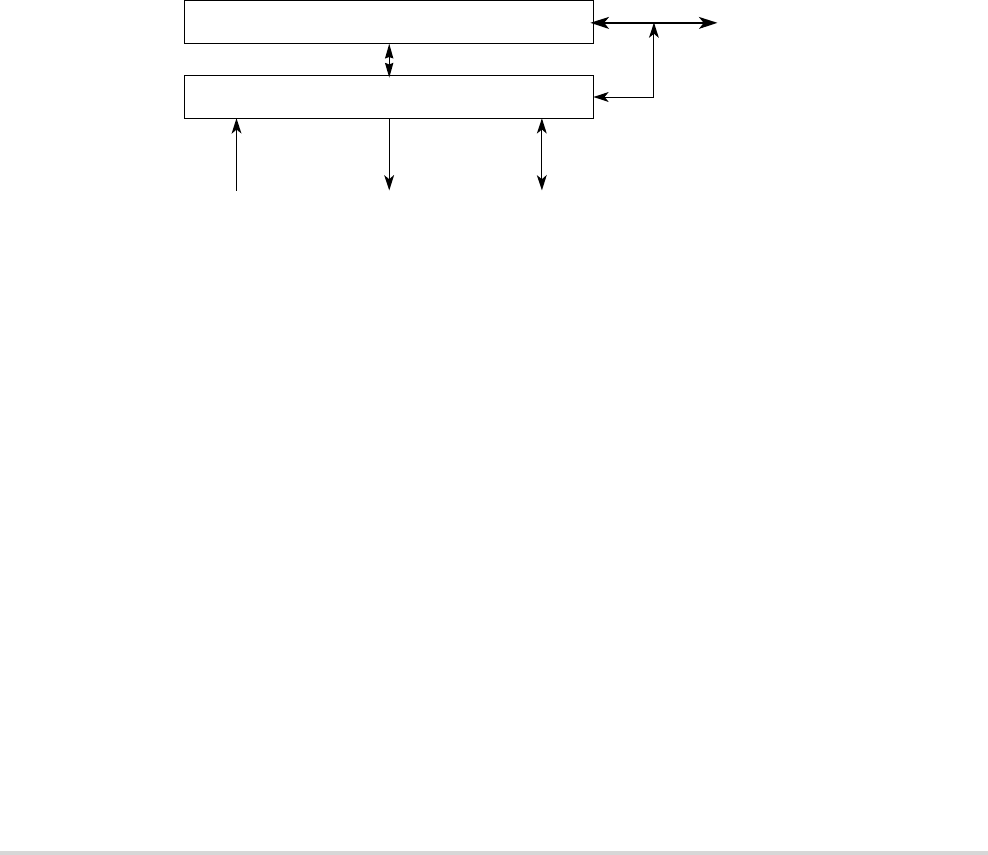
MOTOROLA Chapter 29. Debug Support 29-1
Chapter 29
Debug Support
This chapter describes the Revision A enhanced hardware debug support in the MCF5282.
29.1 Overview
The debug module is shown in Figure 29-1.
Figure 29-1. Processor/Debug Module Interface
Debug support is divided into three areas:
• Real-time trace support—The ability to determine the dynamic execution path
through an application is fundamental for debugging. The ColdFire solution
implements an 8-bit parallel output bus that reports processor execution status and
data to an external emulator system. See Section 29.3, “Real-Time Trace Support.”
• Background debug mode (BDM)—Provides low-level debugging in the ColdFire
processor complex. In BDM, the processor complex is halted and a variety of
commands can be sent to the processor to access memory and registers. The external
emulator uses a three-pin, serial, full-duplex channel. See Section 29.5,
“Background Debug Mode (BDM),” and Section 29.4, “Programming Model.”
• Real-time debug support—BDM requires the processor to be halted, which many
real-time embedded applications cannot do. Debug interrupts let real-time systems
execute a unique service routine that can quickly save the contents of key registers
and variables and return the system to normal operation. External development
ColdFire CPU Core
Debug Module
High-speed
Communication Port
DSCLK, DSI, DSO
Control
BKPT
local bus
Trace Port
PST[3:0], DDATA[3:0]
CLKOUT
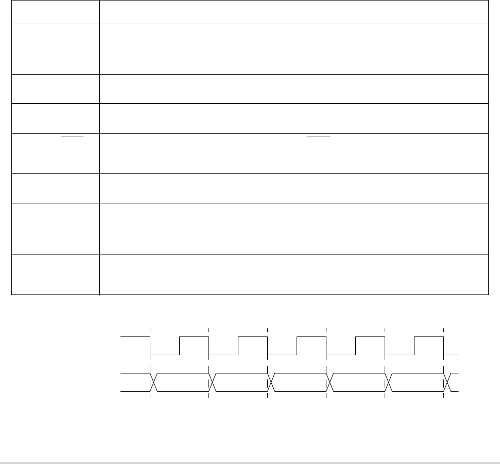
29-2 MCF5282 User’s Manual MOTOROLA
Signal Description
systems can access saved data because the hardware supports concurrent operation
of the processor and BDM-initiated commands. See Section 29.6, “Real-Time
Debug Support.”
NOTE
Enabling Flash security will disable BDM communications.
29.2 Signal Description
Table 29-1 describes debug module signals. All ColdFire debug signals are unidirectional
and related to a rising edge of the processor’s clock signal. The standard 26-pin debug
connector is shown in Section 29.8, “Motorola-Recommended BDM Pinout.”
Figure 29-2 shows CLKOUT timing with respect to PST and DDATA.
Figure 29-2. CLKOUT Timing
Table 29-1. Debug Module Signals
Signal Description
Development Serial
Clock (DSCLK)
Internally synchronized input. (The logic level on DSCLK is validated if it has the same value on two
consecutive rising CLKOUT edges.) Clocks the serial communication port to the debug module during
packet transfers. Maximum frequency is 1/5 the processor status clock (CLKOUT) speed. At the
synchronized rising edge of DSCLK, the data input on DSI is sampled and DSO changes state.
Development Serial
Input (DSI)
Internally synchronized input that provides data input for the serial communication port to the debug
module.
Development Serial
Output (DSO)
Provides serial output communication for debug module responses. DSO is registered internally.
Breakpoint (BKPT) Input used to request a manual breakpoint. Assertion of BKPT puts the processor into a halted state after
the current instruction completes. Halt status is reflected on processor status signals (PST[3:0]) as the
value 0xF.
CLKOUT See Figure 29-2. CLKOUT indicates when the development system should sample PST and DDATA
values.
Debug Data
(DDATA[3:0])
These output signals display the register breakpoint status as a default, or optionally, captured address
and operand values. The capturing of data values is controlled by the setting of the CSR. Additionally,
execution of the WDDATA instruction by the processor captures operands which are displayed on
DDATA. These signals are updated each processor cycle.
Processor Status
(PST[3:0])
These output signals report the processor status. Table 29-2 shows the encoding of these signals. These
outputs indicate the current status of the processor pipeline and, as a result, are not related to the current
bus transfer. The PST value is updated each processor cycle.
CLKOUT
PST or DDATA

MOTOROLA Chapter 29. Debug Support 29-3
Real-Time Trace Support
29.3 Real-Time Trace Support
Real-time trace, which defines the dynamic execution path, is a fundamental debug
function. The ColdFire solution is to include a parallel output port providing encoded
processor status and data to an external development system. This port is partitioned into
two 4-bit nibbles: one nibble allows the processor to transmit processor status, (PST), and
the other allows operand data to be displayed (debug data, DDATA). The processor status
may not be related to the current bus transfer.
External development systems can use PST outputs with an external image of the program
to completely track the dynamic execution path. This tracking is complicated by any
change in flow, especially when branch target address calculation is based on the contents
of a program-visible register (variant addressing). DDATA outputs can be configured to
display the target address of such instructions in sequential nibble increments across
multiple processor clock cycles, as described in Section 29.3.1, “Begin Execution of Taken
Branch (PST = 0x5).” Two 32-bit storage elements form a FIFO buffer connecting the
processor’s high-speed local bus to the external development system through PST[3:0] and
DDATA[3:0]. The buffer captures branch target addresses and certain data values for
eventual display on the DDATA port, one nibble at a time starting with the least significant
bit (lsb).
Execution speed is affected only when both storage elements contain valid data to be
dumped to the DDATA port. The core stalls until one FIFO entry is available.
Table 29-2 shows the encoding of these signals.
Table 29-2. Processor Status Encoding
PST[3:0]
Definition
Hex Binary
0x0 0000 Continue execution. Many instructions execute in one processor cycle. If an instruction requires more processor
clock cycles, subsequent clock cycles are indicated by driving PST outputs with this encoding.
0x1 0001 Begin execution of one instruction. For most instructions, this encoding signals the first processor clock cycle of
an instruction’s execution. Certain change-of-flow opcodes, plus the PULSE and WDDATA instructions,
generate different encodings.
0x2 0010 Reserved
0x3 0011 Entry into user-mode. Signaled after execution of the instruction that caused the ColdFire processor to enter user
mode.
0x4 0100 Begin execution of PULSE and WDDATA instructions. PULSE defines logic analyzer triggers for debug and/or
performance analysis. WDDATA lets the core write any operand (byte, word, or longword) directly to the
DDATA port, independent of debug module configuration. When WDDATA is executed, a value of 0x4 is
signaled on the PST port, followed by the appropriate marker, and then the data transfer on the DDATA port.
Transfer length depends on the WDDATA operand size.
0x5 0101 Begin execution of taken branch. For some opcodes, a branch target address may be displayed on DDATA
depending on the CSR settings. CSR also controls the number of address bytes displayed, indicated by the PST
marker value preceding the DDATA nibble that begins the data output. See Section 29.3.1, “Begin Execution of
Taken Branch (PST = 0x5).”
0x6 0110 Reserved

29-4 MCF5282 User’s Manual MOTOROLA
Real-Time Trace Support
29.3.1 Begin Execution of Taken Branch (PST = 0x5)
PST is 0x5 when a taken branch is executed. For some opcodes, a branch target address may
be displayed on DDATA depending on the CSR settings. CSR also controls the number of
address bytes displayed, which is indicated by the PST marker value immediately
preceding the DDATA nibble that begins the data output.
Bytes are displayed in least-to-most-significant order. The processor captures only those
target addresses associated with taken branches which use a variant addressing mode, that
is, RTE and RTS instructions, JMP and JSR instructions using address register indirect or
indexed addressing modes, and all exception vectors.
The simplest example of a branch instruction using a variant address is the compiled code
for a C language case statement. Typically, the evaluation of this statement uses the variable
of an expression as an index into a table of offsets, where each offset points to a unique case
within the structure. For such change-of-flow operations, the MCF5282 uses the debug pins
to output the following sequence of information on successive processor clock cycles:
1. Use PST (0x5) to identify that a taken branch was executed.
2. Using the PST pins, optionally signal the target address to be displayed sequentially
on the DDATA pins. Encodings 0x9–0xB identify the number of bytes displayed.
3. The new target address is optionally available on subsequent cycles using the
DDATA port. The number of bytes of the target address displayed on this port is
configurable (2, 3, or 4 bytes).
0x7 0111 Begin execution of return from exception (RTE) instruction.
0x8–
0xB
1000–1
011
Indicates the number of bytes to be displayed on the DDATA port on subsequent processor clock cycles. The
value is driven onto the PST port one CLKOUT cycle before the data is displayed on DDATA.
0x8 Begin 1-byte transfer on DDATA.
0x9 Begin 2-byte transfer on DDATA.
0xA Begin 3-byte transfer on DDATA.
0xB Begin 4-byte transfer on DDATA.
0xC 1100 Exception processing. Exceptions that enter emulation mode (debug interrupt or optionally trace) generate a
different encoding, as described below. Because the 0xC encoding defines a multiple-cycle mode, PST outputs
are driven with 0xC until exception processing completes.
0xD 1101 Entry into emulator mode. Displayed during emulation mode (debug interrupt or optionally trace). Because this
encoding defines a multiple-cycle mode, PST outputs are driven with 0xD until exception processing completes.
0xE 1110 Processor is stopped. Appears in multiple-cycle format when the MCF5282 executes a STOP instruction. The
ColdFire processor remains stopped until an interrupt occurs, thus PST outputs display 0xE until the stopped
mode is exited.
0xF 1111 Processor is halted. Because this encoding defines a multiple-cycle mode, the PST outputs display 0xF until the
processor is restarted or reset. (see Section 29.5.1, “CPU Halt”)
Table 29-2. Processor Status Encoding (continued)
PST[3:0]
Definition
Hex Binary

MOTOROLA Chapter 29. Debug Support 29-5
Programming Model
Another example of a variant branch instruction would be a JMP (A0) instruction.
Figure 29-3 shows the PST and DDATA outputs that indicate a JMP (A0) execution
(assuming the CSR was programmed to display the lower 2 bytes of an address).
Figure 29-3. Example JMP Instruction Output on PST/DDATA
PST 0x5 indicates a taken branch and the marker value 0x9 indicates a 2-byte address.
Thus, the subsequent 4 nibbles of DDATA display the lower 2 bytes of address register A0
in least-to-most-significant nibble order. The PST output after the JMP instruction
completes depends on the target instruction. The PST can continue with the next instruction
before the address has completely displayed on DDATA because of the DDATA FIFO. If
the FIFO is full and the next instruction has captured values to display on DDATA, the
pipeline stalls (PST = 0x0) until space is available in the FIFO.
29.4 Programming Model
In addition to the existing BDM commands that provide access to the processor’s registers
and the memory subsystem, the debug module contains 19 registers to support the required
functionality. These registers are also accessible from the processor’s supervisor
programming model by executing the WDEBUG instruction (write only). Thus, the
breakpoint hardware in the debug module can be written by the external development
system using the debug serial interface or by the operating system running on the processor
core. Software is responsible for guaranteeing that accesses to these resources are serialized
and logically consistent. Hardware provides a locking mechanism in the CSR to allow the
external development system to disable any attempted writes by the processor to the
breakpoint registers (setting CSR[IPW]). BDM commands must not be issued if the
MCF5282 is using the WDEBUG instruction to access debug module registers or the
resulting behavior is undefined.
These registers, shown in Figure 29-4, are treated as 32-bit quantities, regardless of the
number of implemented bits.
DDATA
CLKOUT
0x0 0x0 A[3:0]
0x5 0x9 default
PST
A[7:4] A[11:8] A[15:12]
default default default
29-6 MCF5282 User’s Manual MOTOROLA
Programming Model
Figure 29-4. Debug Programming Model
These registers are accessed through the BDM port by the commands, WDMREG and
RDMREG, described in Section 29.5.3.3, “Command Set Descriptions.” These commands
contain a 5-bit field, DRc, that specifies the register, as shown in Table 29-3.
PC breakpoint mask register
PC breakpoint register
Data breakpoint register
Data breakpoint mask register
Trigger definition register
Configuration/status register
Note: Each debug register is accessed as a 32-bit register; shaded fields above are not used (don’t care).
All debug control registers are writable from the external development system or the CPU via the WDEBUG
instruction. CSR is write-only from the programming model. It can be read or written through the BDM port using the
RDMREG and WDMREG commands.
Address attribute trigger register
Address low breakpoint register
Address high breakpoint register
31 15 7 0
31 15 0
31 15 0
31 15 0
31 15 0
31 15 0
AATR
ABLR
ABHR
CSR
DBR
DBMR
PBR
PBMR
TDR
PC breakpoint mask register
PC breakpoint register
Data breakpoint register
Data breakpoint mask register
Trigger definition register
Configuration/status register
BDM address attribute register
Note: Each debug register is accessed as a 32-bit register; shaded fields above are not used (don’t care).
All debug control registers are writable from the external development system or the CPU via the WDEBUG
instruction.
CSR is write-only from the programming model. It can be read or written through the BDM port using the RDMREG
and WDMREG commands.
Address attribute trigger register
Address low breakpoint register
Address high breakpoint register
31 15 7 0
31 15 7 0
31 15 0
31 15 0
31 15 0
31 15 0
31 15 0
31 15 0
AATR
ABLR
ABHR
BAAR
CSR
DBR
DBMR
PBR
PBMR
TDR

MOTOROLA Chapter 29. Debug Support 29-7
Programming Model
NOTE:
Debug control registers can be written by the external
development system or the CPU through the WDEBUG
instruction.
CSR is write-only from the programming model. It can be read
or written through the BDM port using the RDMREG and
WDMREG commands.
29.4.1 Revision A Shared Debug Resources
In the Revision A implementation of the debug module, certain hardware structures are
shared between BDM and breakpoint functionality as shown in Table 29-4.
Thus, loading a register to perform a specific function that shares hardware resources is
destructive to the shared function. For example, a BDM command to access memory
overwrites an address breakpoint in ABHR. A BDM write command overwrites the data
breakpoint in DBR.
Table 29-3. BDM/Breakpoint Registers
DRc[4–0] Register Name Abbreviation Initial State Page
0x00 Configuration/status register CSR 0x00010_0000 p. 29-10
0x01–0x05 Reserved — — —
0x06 Address attribute trigger register AATR 0x0000_0005 p. 29-8
0x07 Trigger definition register TDR 0x0000_0000 p. 29-14
0x08 Program counter breakpoint register PBR — p. 29-13
0x09 Program counter breakpoint mask register PBMR — p. 29-13
0x0A–0x0B Reserved — — —
0x0C Address breakpoint high register ABHR — p. 29-9
0x0D Address breakpoint low register ABLR — p. 29-9
0x0E Data breakpoint register DBR — p. 29-12
0x0F Data breakpoint mask register DBMR — p. 29-12
Table 29-4. Rev. A Shared BDM/Breakpoint Hardware
Register BDM Function Breakpoint Function
AATR Bus attributes for all memory commands Attributes for address breakpoint
ABHR Address for all memory commands Address for address breakpoint
DBR Data for all BDM write commands Data for data breakpoint

29-8 MCF5282 User’s Manual MOTOROLA
Programming Model
29.4.2 Address Attribute Trigger Register (AATR)
The AATR, shown in Figure 29-5, defines address attributes and a mask to be matched in
the trigger. The register value is compared with address attribute signals from the
processor’s local high-speed bus, as defined by the setting of the trigger definition register
(TDR).
Table 29-5 describes AATR fields.
15 14 13 12 11 10 8 7 6 5 4 3 2 0
Field RM SZM TTM TMM R SZ TT TM
Reset 0000_0000_0000_0101
R/W Write only. AATR is accessible in supervisor mode as debug control register 0x06 using the WDEBUG instruction
and through the BDM port using the WDMREG command.
DRc[4–0] 0x06
Figure 29-5. Address Attribute Trigger Register (AATR)
Table 29-5. AATR Field Descriptions
Bits Name Description
15 RM Read/write mask. Setting RM masks R in address comparisons.
14–13 SZM Size mask. Setting an SZM bit masks the corresponding SZ bit in address comparisons.
12–11 TTM Transfer type mask. Setting a TTM bit masks the corresponding TT bit in address comparisons.
10–8 TMM Transfer modifier mask. Setting a TMM bit masks the corresponding TM bit in address comparisons.
7 R Read/write. R is compared with the R/W signal of the processor’s local bus.
6–5 SZ Size. Compared to the processor’s local bus size signals.
00 Longword
01 Byte
10 Word
11 Reserved
4–3 TT Transfer type. Compared with the local bus transfer type signals.
00 Normal processor access
01 Reserved
10 Emulator mode access
11 Acknowledge/CPU space access
These bits also define the TT encoding for BDM memory commands. In this case, the 01 encoding indicates
an external or DMA access (for backward compatibility). These bits affect the TM bits.

MOTOROLA Chapter 29. Debug Support 29-9
Programming Model
29.4.3 Address Breakpoint Registers (ABLR, ABHR)
The ABLR and ABHR, shown in Figure 29-6, define regions in the processor’s data
address space that can be used as part of the trigger. These register values are compared
with the address for each transfer on the processor’s high-speed local bus. The trigger
definition register (TDR) identifies the trigger as one of three cases:
1. Identical to the value in ABLR
2. Inside the range bound by ABLR and ABHR inclusive
3. Outside that same range
2–0 TM Transfer modifier. Compared with the local bus transfer modifier signals, which give supplemental
information for each transfer type.
TT = 00 (normal mode):
000 Explicit cache line push
001 User data access
010 User code access
011 Reserved
100 Reserved
101 Supervisor data access
110 Supervisor code access
111 Reserved
TT = 10 (emulator mode):
0xx–100 Reserved
101 Emulator mode data access
110 Emulator mode code access
111 Reserved
TT = 11 (acknowledge/CPU space transfers):
000 CPU space access
001–111 Interrupt acknowledge levels 1–7
These bits also define the TM encoding for BDM memory commands (for backward compatibility).
31 0
Field Address
Reset —
R/W Write only. ABHR is accessible in supervisor mode as debug control register 0x0C using the WDEBUG instruction
and via the BDM port using the RDMREG and WDMREG commands.
ABLR is accessible in supervisor mode as debug control register 0x0D using the WDEBUG instruction and via the
BDM port using the WDMREG command.
DRc[4–0] 0x0D (ABLR); 0x0C (ABHR)
Figure 29-6. Address Breakpoint Registers (ABLR, ABHR)
Table 29-5. AATR Field Descriptions (continued)
Bits Name Description
29-10 MCF5282 User’s Manual MOTOROLA
Programming Model
Table 29-6 describes ABLR fields.
Table 29-7 describes ABHR fields.
29.4.4 Configuration/Status Register (CSR)
The CSR defines the debug configuration for the processor and memory subsystem and
contains status information from the breakpoint logic. CSR is write-only from the
programming model. It can be read from and written to through the BDM port. CSR is
accessible in supervisor mode as debug control register 0x00 using the WDEBUG
instruction and through the BDM port using the RDMREG and WDMREG commands.
Table 29-6. ABLR Field Description
Bits Name Description
31–0 Address Low address. Holds the 32-bit address marking the lower bound of the address breakpoint range.
Breakpoints for specific addresses are programmed into ABLR.
Table 29-7. ABHR Field Description
Bits Name Description
31–0 Address High address. Holds the 32-bit address marking the upper bound of the address breakpoint range.
31 28 27 26 25 24 23 20 19 17 16
Field BSTAT FOF TRG HAL
T
BKPT HRL — IPW
Reset 0000_0000_0000_0000
R/W1R—R/W
15 14 13 12 11 10 9 8 7 6 5 4 3 0
Field MAP TRC EMU DDC UHE BTB — NPL IPI SSM —
Reset 0000_0000_0000_0000
R/W R/W R/W R/W R/W R/W R/W R R/W R/W R/W —
DRc[4–0] 0000_0000_0000_0000
Figure 29-7. Configuration/Status Register (CSR)

MOTOROLA Chapter 29. Debug Support 29-11
Programming Model
Table 29-8 describes CSR fields.
Table 29-8. CSR Field Descriptions
Bit Name Description
31–28 BSTAT Breakpoint status. Provides read-only status information concerning hardware breakpoints. BSTAT is
cleared by a TDR write or by a CSR read when either a level-2 breakpoint is triggered or a level-1
breakpoint is triggered and the level-2 breakpoint is disabled.
0000 No breakpoints enabled
0001 Waiting for level-1 breakpoint
0010 Level-1 breakpoint triggered
0101 Waiting for level-2 breakpoint
0110 Level-2 breakpoint triggered
27 FOF Fault-on-fault. If FOF is set, a catastrophic halt occurred and forced entry into BDM. FOF is cleared
whenever CSR is read.
26 TRG Hardware breakpoint trigger. If TRG is set, a hardware breakpoint halted the processor core and forced entry
into BDM. Reset, the debug GO command, or reading CSR will clear TRG.
25 HALT Processor halt. If HALT is set, the processor executed a HALT and forced entry into BDM. Reset, the debug
GO command, or reading CSR will clear HALT.
24 BKPT Breakpoint assert. If BKPT is set, BKPT was asserted, forcing the processor into BDM. Reset, the debug GO
command, or reading CSR will clear BKPT.
23–20 HRL Hardware revision level. Indicates the level of debug module functionality. An emulator could use this
information to identify the level of functionality supported.
0000 Initial debug functionality (Revision A) (This is the only valid value for the MCF5282.)
19–17 — Reserved, should be cleared.
16 IPW Inhibit processor writes. Setting IPW inhibits processor-initiated writes to the debug module’s programming
model registers. IPW can be modified only by commands from the external development system.
15 MAP Force processor references in emulator mode.
0 All emulator-mode references are mapped into supervisor code and data spaces.
1 The processor maps all references while in emulator mode to a special address space, TT = 10, TM = 101
or 110.
14 TRC Force emulation mode on trace exception. If TRC = 1, the processor enters emulator mode when a trace
exception occurs. If TRC=0, the processor enters supervisor mode.
13 EMU Force emulation mode. If EMU = 1, the processor begins executing in emulator mode. See Section 29.6.1.1,
“Emulator Mode.”
12–11 DDC Debug data control. Controls operand data capture for DDATA, which displays the number of bytes defined
by the operand reference size before the actual data; byte displays 8 bits, word displays 16 bits, and long
displays 32 bits (one nibble at a time across multiple PSTCLK cycles). See Table 29-2.
00 No operand data is displayed.
01 Capture all write data.
10 Capture all read data.
11 Capture all read and write data.
10 UHE User halt enable. Selects the CPU privilege level required to execute the HALT instruction.
0 HALT is a supervisor-only instruction.
1 HALT is a supervisor/user instruction.
9–8 BTB Branch target bytes. Defines the number of bytes of branch target address DDATA displays.
00 0 bytes
01 Lower 2 bytes of the target address
10 Lower 3 bytes of the target address
11 Entire 4-byte target address
See Section 29.3.1, “Begin Execution of Taken Branch (PST = 0x5).”

29-12 MCF5282 User’s Manual MOTOROLA
Programming Model
29.4.5 Data Breakpoint/Mask Registers (DBR, DBMR)
The DBR, shown in Figure 29-8, specifies data patterns used as part of the trigger into
debug mode. DBR bits are masked by setting corresponding DBMR bits, as defined in
TDR.
7 — Reserved, should be cleared.
6 NPL Non-pipelined mode. Determines whether the core operates in pipelined or mode or not.
0 Pipelined mode
1 Nonpipelined mode. The processor effectively executes one instruction at a time with no overlap. This
adds at least 5 cycles to the execution time of each instruction. Given an average execution latency of 1.6
cycles/instruction, throughput in non-pipeline mode would be 6.6 cycles/instruction, approximately 25%
or less of pipelined performance.
Regardless of the NPL state, a triggered PC breakpoint is always reported before the triggering instruction
executes. In normal pipeline operation, the occurrence of an address and/or data breakpoint trigger is
imprecise. In non-pipeline mode, triggers are always reported before the next instruction begins execution
and trigger reporting can be considered precise.
5 IPI Ignore pending interrupts.
1 Core ignores any pending interrupt requests signalled while in single-instruction-step mode.
0 Core services any pending interrupt requests that were signalled while in single-step mode.
4 SSM Single-step mode. Setting SSM puts the processor in single-step mode.
0 Normal mode.
1 Single-step mode. The processor halts after execution of each instruction. While halted, any BDM
command can be executed. On receipt of the GO command, the processor executes the next instruction and
halts again. This process continues until SSM is cleared.
3–0 — Reserved, should be cleared.
31 0
Field Data (DBR); Mask (DBMR)
Reset Uninitialized
R/W DBR is accessible in supervisor mode as debug control register 0x0E, using the WDEBUG instruction and through the
BDM port using the RDMREG and WDMREG commands.
DBMR is accessible in supervisor mode as debug control register 0x0F,using the WDEBUG instruction and via the
BDM port using the WDMREG command.
DRc[4–0] 0x0E (DBR), 0x0F (DBMR)
Figure 29-8. Data Breakpoint/Mask Registers (DBR/DBMR)
Table 29-8. CSR Field Descriptions (continued)
Bit Name Description
MOTOROLA Chapter 29. Debug Support 29-13
Programming Model
Table 29-9 describes DBR fields.
Table 29-10 describes DBMR fields.
The DBR supports both aligned and misaligned references. Table 29-11 shows
relationships between processor address, access size, and location within the 32-bit data
bus.
29.4.6 Program Counter Breakpoint/Mask Registers
(PBR, PBMR)
The PBR defines an instruction address for use as part of the trigger. This register’s contents
are compared with the processor’s program counter register when TDR is configured
appropriately. PBR bits are masked by setting corresponding PBMR bits. Results are
compared with the processor’s program counter register, as defined in TDR. Figure 29-9
shows the PC breakpoint register.
Table 29-9. DBR Field Descriptions
Bits Name Description
31–0 Data Data breakpoint value. Contains the value to be compared with the data value from the processor’s local bus
as a breakpoint trigger.
Table 29-10. DBMR Field Descriptions
Bits Name Description
31–0 Mask Data breakpoint mask. The 32-bit mask for the data breakpoint trigger. Clearing a DBR bit allows the
corresponding DBR bit to be compared to the appropriate bit of the processor’s local data bus. Setting a
DBMR bit causes that bit to be ignored.
Table 29-11. Access Size and Operand Data Location
A[1:0] Access Size Operand Location
00 Byte D[31:24]
01 Byte D[23:16]
10 Byte D[15:8]
11 Byte D[7:0]
0x Word D[31:16]
1x Word D[15:0]
xx Longword D[31:0]

29-14 MCF5282 User’s Manual MOTOROLA
Programming Model
Table 29-12 describes PBR fields.
Figure 29-9 shows PBMR.
Table 29-13 describes PBMR fields.
29.4.7 Trigger Definition Register (TDR)
The TDR, shown in Table 29-11, configures the operation of the hardware breakpoint logic
that corresponds with the ABHR/ABLR/AATR, PBR/PBMR, and DBR/DBMR registers
within the debug module. The TDR controls the actions taken under the defined conditions.
Breakpoint logic may be configured as a one- or two-level trigger. TDR[31–16] define the
second-level trigger and bits 15–0 define the first-level trigger.
31 0
Field Program Counter
Reset —
R/W Write. PC breakpoint register is accessible in supervisor mode using the WDEBUG instruction and through the BDM
port using the RDMREG and WDMREG commands using values shown in Section 29.5.3.3, “Command Set
Descriptions.”
DRc[4–0] 0x08
Figure 29-9. Program Counter Breakpoint Register (PBR)
Table 29-12. PBR Field Descriptions
Bits Name Description
31–0 Address PC breakpoint address. The 32-bit address to be compared with the PC as a breakpoint trigger.
31 0
Field Mask
Reset —
R/W Write. PBMR is accessible in supervisor mode as debug control register 0x09 using the WDEBUG instruction and
via the BDM port using the wdmreg command.
DRc[4–0] 0x09
Figure 29-10. Program Counter Breakpoint Mask Register (PBMR)
Table 29-13. PBMR Field Descriptions
Bits Name Description
31–0 Mask PC breakpoint mask. A zero in a bit position causes the corresponding PBR bit to be compared to the
appropriate PC bit. Set PBMR bits cause PBR bits to be ignored.

MOTOROLA Chapter 29. Debug Support 29-15
Programming Model
NOTE:
The debug module has no hardware interlocks, so to prevent
spurious breakpoint triggers while the breakpoint registers are
being loaded, disable TDR (by clearing TDR[29,13])before
defining triggers.
A write to TDR clears the CSR trigger status bits, CSR[BSTAT].
Table 29-14 describes TDR fields.
31 30 29 28 27 26 25 24 23 22 21 20 19 18 17 16
Field TRC EBL EDLW EDWL EDWU EDLL EDLM EDUM EDUU DI EAI EAR EAL EPC PCI
Reset 0000_0000_0000_0000
151413 12 11 10 9 8 7 6 543210
Field LxT EBL EDLW EDWL EDWU EDLL EDLM EDUM EDUU DI EAI EAR EAL EPC PCI
Reset 0000_0000_0000_0000
R/W Write only. Accessible in supervisor mode as debug control register 0x07 using the WDEBUG instruction and through the
BDM port using the WDMREG command.
DRc[4–0] 0x07
Figure 29-11. Trigger Definition Register (TDR)
Table 29-14. TDR Field Descriptions
Bits Name Description
31–30 TRC Trigger response control. Determines how the processor responds to a completed trigger condition. The
trigger response is always displayed on DDATA.
00 Display on DDATA only
01 Processor halt
10 Debug interrupt
11 Reserved
15–14 LxT Level-x trigger. This is a Rev. B function only. The Level-x Trigger bit determines the logic operation for the
trigger between the PC_condition and the (Address_range & Data_condition) where the inclusion of a Data
condition is optional. The ColdFire debug architecture supports the creation of single or double-level triggers.
TDR[15]
0 Level-2 trigger = PC_condition & Address_range & Data_condition
1 Level-2 trigger = PC_condition | (Address_range & Data_condition)
TDR[14]
0 Level-1 trigger = PC_condition & Address_range & Data_condition
1 Level-1 trigger = PC_condition | (Address_range & Data_condition)
29/13 EBL Enable breakpoint. Global enable for the breakpoint trigger. Setting TDR[EBL] enables a breakpoint trigger.
Clearing it disables all breakpoints at that level.
Second-Level Trigger
First-Level Trigger

29-16 MCF5282 User’s Manual MOTOROLA
Background Debug Mode (BDM)
29.5 Background Debug Mode (BDM)
The ColdFire Family implements a low-level system debugger in the microprocessor
hardware. Communication with the development system is handled through a dedicated,
high-speed serial command interface. The ColdFire architecture implements the BDM
controller in a dedicated hardware module. Although some BDM operations, such as CPU
register accesses, require the CPU to be halted, other BDM commands, such as memory
accesses, can be executed while the processor is running.
29.5.1 CPU Halt
Although most BDM operations can occur in parallel with CPU operations, unrestricted
BDM operation requires the CPU to be halted. The sources that can cause the CPU to halt
are listed below in order of priority:
28–22/
12–6
EDxSetting an EDx bit enables the corresponding data breakpoint condition based on the size and placement on
the processor’s local data bus. Clearing all EDx bits disables data breakpoints.
28/12 EDLW Data longword. Entire processor’s local data bus.
27/11 EDWL Lower data word.
26/10 EDWU Upper data word.
25/9 EDLL Lower lower data byte. Low-order byte of the low-order word.
24/8 EDLM Lower middle data byte. High-order byte of the low-order word.
23/7 EDUM Upper middle data byte. Low-order byte of the high-order word.
22/6 EDUU Upper upper data byte. High-order byte of the high-order word.
21/5 DI Data breakpoint invert. Provides a way to invert the logical sense of all the data breakpoint comparators. This
can develop a trigger based on the occurrence of a data value other than the DBR contents.
20–18/
4–2
EAxEnable address bits. Setting an EA bit enables the corresponding address breakpoint. Clearing all three bits
disables the breakpoint.
20/4 EAI Enable address breakpoint inverted. Breakpoint is based outside the range between ABLR and
ABHR.
19/3 EAR Enable address breakpoint range. The breakpoint is based on the inclusive range defined by ABLR
and ABHR.
18/2 EAL Enable address breakpoint low. The breakpoint is based on the address in the ABLR.
17/1 EPC Enable PC breakpoint. If set, this bit enables the PC breakpoint.
16/0 PCI Breakpoint invert. If set, this bit allows execution outside a given region as defined by PBR and PBMR to
enable a trigger. If cleared, the PC breakpoint is defined within the region defined by PBR and PBMR.
Table 29-14. TDR Field Descriptions (continued)
Bits Name Description

MOTOROLA Chapter 29. Debug Support 29-17
Background Debug Mode (BDM)
1. A catastrophic fault-on-fault condition automatically halts the processor.
2. A hardware breakpoint can be configured to generate a pending halt condition
similar to the assertion of BKPT. This type of halt is always first made pending in
the processor. Next, the processor samples for pending halt and interrupt conditions
once per instruction. When a pending condition is asserted, the processor halts
execution at the next sample point. See Section 29.6.1, “Theory of Operation.”
3. The execution of a HALT instruction immediately suspends execution. Attempting
to execute HALT in user mode while CSR[UHE] = 0 generates a privilege violation
exception. If CSR[UHE] = 1, HALT can be executed in user mode. After HALT
executes, the processor can be restarted by serial shifting a GO command into the
debug module. Execution continues at the instruction after HALT.
4. The assertion of the BKPT input is treated as a pseudo-interrupt; that is, the halt
condition is postponed until the processor core samples for halts/interrupts. The
processor samples for these conditions once during the execution of each
instruction. If there is a pending halt condition at the sample time, the processor
suspends execution and enters the halted state.
The assertion of BKPT should be considered in the following two special cases:
• After the system reset signal is negated, the processor waits for 16 processor clock
cycles before beginning reset exception processing. If the BKPT input is asserted
within eight cycles after RSTI is negated, the processor enters the halt state,
signaling halt status (0xF) on the PST outputs. While the processor is in this state,
all resources accessible through the debug module can be referenced. This is the
only chance to force the processor into emulation mode through CSR[EMU].
After system initialization, the processor’s response to the GO command depends on
the set of BDM commands performed while it is halted for a breakpoint.
Specifically, if the PC register was loaded, the GO command causes the processor to
exit halted state and pass control to the instruction address in the PC, bypassing
normal reset exception processing. If the PC was not loaded, the GO command
causes the processor to exit halted state and continue reset exception processing.
• The ColdFire architecture also handles a special case of BKPT being asserted while
the processor is stopped by execution of the STOP instruction. For this case, the
processor exits the stopped mode and enters the halted state, at which point, all BDM
commands may be exercised. When restarted, the processor continues by executing
the next sequential instruction, that is, the instruction following the STOP opcode.
CSR[27–24] indicates the halt source, showing the highest priority source for multiple halt
conditions.
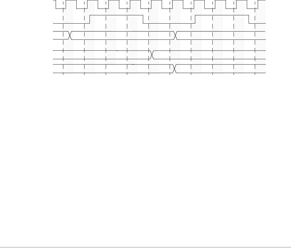
29-18 MCF5282 User’s Manual MOTOROLA
Background Debug Mode (BDM)
29.5.2 BDM Serial Interface
When the CPU is halted and PST reflects the halt status, the development system can send
unrestricted commands to the debug module. The debug module implements a synchronous
protocol using two inputs (DSCLK and DSI) and one output (DSO), where DSO is
specified as a delay relative to the rising edge of the processor clock. See Table 29-1. The
development system serves as the serial communication channel master and must generate
DSCLK.
The serial channel operates at a frequency from DC to 1/5 of the CLKOUT frequency. The
channel uses full-duplex mode, where data is sent and received simultaneously by both
master and slave devices. The transmission consists of 17-bit packets composed of a
status/control bit and a 16-bit data word. As shown in Figure 29-12, all state transitions are
enabled on a rising edge of CLKOUT when DSCLK is high; that is, DSI is sampled and
DSO is driven.
Figure 29-12. BDM Serial Interface Timing
DSCLK and DSI are synchronized inputs. DSCLK acts as a pseudo clock enable and is
sampled on the rising edge of the processor clock as well as the DSI. DSO is delayed from
the DSCLK-enabled CLK rising edge (registered after a BDM state machine state change).
All events in the debug module’s serial state machine are based on the processor clock
rising edge. DSCLK must also be sampled low (on a positive edge of CLK) between each
bit exchange. The MSB is transferred first. Because DSO changes state based on an
internally-recognized rising edge of DSCLK, DSDO cannot be used to indicate the start of
a serial transfer. The development system must count clock cycles in a given transfer.
C1–C4 are described as follows:
• C1—First synchronization cycle for DSI (DSCLK is high).
• C2—Second synchronization cycle for DSI (DSCLK is high).
• C3—BDM state machine changes state depending upon DSI and whether the entire
input data transfer has been transmitted.
• C4—DSO changes to next value.
CLKOUT
DSCLK
Next State
BDM State
Machine
DSO
DSI
Current State
Current Next
Past Current
C1 C2 C3 C4

MOTOROLA Chapter 29. Debug Support 29-19
Background Debug Mode (BDM)
NOTE:
A not-ready response can be ignored except during a
memory-referencing cycle. Otherwise, the debug module can
accept a new serial transfer after 32 processor clock periods.
29.5.2.1 Receive Packet Format
The basic receive packet, Figure 29-13, consists of 16 data bits and 1 status bit
.
Table 29-15 describes receive BDM packet fields.
29.5.2.2 Transmit Packet Format
The basic transmit packet, Figure 29-14, consists of 16 data bits and 1 control bit.
Table 29-16 describes transmit BDM packet fields.
16 15 0
S Data Field [15:0]
Figure 29-13. Receive BDM Packet
Table 29-15. Receive BDM Packet Field Description
Bits Name Description
16 S Status. Indicates the status of CPU-generated messages listed below. The not-ready response can be ignored
unless a memory-referencing cycle is in progress. Otherwise, the debug module can accept a new serial transfer
after 32 processor clock periods.
SData Message
0 xxxx Valid data transfer
0 0xFFFF Status OK
1 0x0000 Not ready with response; come again
1 0x0001 Error—Terminated bus cycle; data invalid
1 0xFFFF Illegal command
15–0 D Data. Contains the message to be sent from the debug module to the development system. The response
message is always a single word, with the data field encoded as shown above.
16 15 0
CD
Figure 29-14. Transmit BDM Packet
Table 29-16. Transmit BDM Packet Field Description
Bits Name Description
16 C Control. This bit is reserved. Command and data transfers initiated by the development system should clear C.
15–0 D Data bits 15–0. Contains the data to be sent from the development system to the debug module.

29-20 MCF5282 User’s Manual MOTOROLA
Background Debug Mode (BDM)
29.5.3 BDM Command Set
Table 29-17 summarizes the BDM command set. Subsequent paragraphs contain detailed
descriptions of each command. Issuing a BDM command when the processor is accessing
debug module registers using the WDEBUG instruction causes undefined behavior.
Unassigned command opcodes are reserved by Motorola. All unused command formats
within any revision level perform a NOP and return the illegal command response.
Table 29-17. BDM Command Summary
Command Mnemonic Description CPU
State 1
1General command effect and/or requirements on CPU operation:
- Halted. The CPU must be halted to perform this command.
- Steal. Command generates bus cycles that can be interleaved with bus accesses.
- Parallel. Command is executed in parallel with CPU activity.
Section Command
(Hex)
Read A/D
register
RAREG/
RDREG
Read the selected address or data register and return the
results through the serial interface.
Halted 29.5.3.3.1 0x218 {A/D,
Reg[2:0]}
Write A/D
register
WAREG/
WDREG
Write the data operand to the specified address or data
register.
Halted 29.5.3.3.2 0x208 {A/D,
Reg[2:0]}
Read memory
location
READ Read the data at the memory location specified by the
longword address.
Steal 29.5.3.3.3 0x1900—byte
0x1940—word
0x1980—lword
Write memory
location
WRITE Write the operand data to the memory location specified
by the longword address.
Steal 29.5.3.3.4 0x1800—byte
0x1840—word
0x1880—lword
Dump
memory block
DUMP Used with READ to dump large blocks of memory. An
initial READ is executed to set up the starting address of
the block and to retrieve the first result. A DUMP
command retrieves subsequent operands.
Steal 29.5.3.3.5 0x1D00—byte
0x1D40—word
0x1D80—lword
Fill memory
block
FILL Used with WRITE to fill large blocks of memory. An
initial WRITE is executed to set up the starting address of
the block and to supply the first operand. A FILL
command writes subsequent operands.
Steal 29.5.3.3.6 0x1C00—byte
0x1C40—word
0x1C80—lword
Resume
execution
GO The pipeline is flushed and refilled before resuming
instruction execution at the current PC.
Halted 29.5.3.3.7 0x0C00
No operation NOP Perform no operation; may be used as a null command. Parallel 29.5.3.3.8 0x0000
Read control
register
RCREG Read the system control register. Halted 29.5.3.3.9 0x2980
Write control
register
WCREG Write the operand data to the system control register. Halted 29.5.3.3.10 0x2880
Read debug
module
register
RDMREG Read the debug module register. Parallel 29.5.3.3.11 0x2D {0x4 2
DRc[4:0]}
20x4 is a three-bit field.
Write debug
module
register
WDMREG Write the operand data to the debug module register. Parallel 29.5.3.3.12 0x2C {0x42
DRc[4:0]}

MOTOROLA Chapter 29. Debug Support 29-21
Background Debug Mode (BDM)
29.5.3.1 ColdFire BDM Command Format
All ColdFire Family BDM commands include a 16-bit operation word followed by an
optional set of one or more extension words, as shown in Figure 29-15.
Table 29-18 describes BDM fields.
29.5.3.1.1 Extension Words as Required
Some commands require extension words for addresses and/or immediate data. Addresses
require two extension words because only absolute long addressing is permitted. Longword
accesses are forcibly longword-aligned and word accesses are forcibly word-aligned.
Immediate data can be 1 or 2 words long. Byte and word data each requires a single
extension word and longword data requires two extension words.
Operands and addresses are transferred most-significant word first. In the following
descriptions of the BDM command set, the optional set of extension words is defined as
address, data, or operand data.
15 1098765432 0
Operation 0 R/W Op Size 0 0 A/D Register
Extension Word(s)
Figure 29-15. BDM Command Format
Table 29-18. BDM Field Descriptions
Bit Name Description
15–10 Operation Specifies the command. These values are listed in Table 29-17.
9 0 Reserved, should be cleared.
8 R/W Direction of operand transfer.
0 Data is written to the CPU or to memory from the development system.
1 The transfer is from the CPU to the development system.
7–6 Op Size Operand data size for sized operations. Addresses are expressed as 32-bit absolute values. Note that a
command performing a byte-sized memory read leaves the upper 8 bits of the response data undefined.
Referenced data is returned in the lower 8 bits of the response.
Operand Size Bit Values
00 Byte 8 bits
01 Word 16 bits
10 Longword 32 bits
11 Reserved —
5–4 00 Reserved, should be cleared.
3 A/D Address/data. Determines whether the register field specifies a data or address register.
0 Indicates a data register.
1 Indicates an address register.
2–0 Register Contains the register number in commands that operate on processor registers.
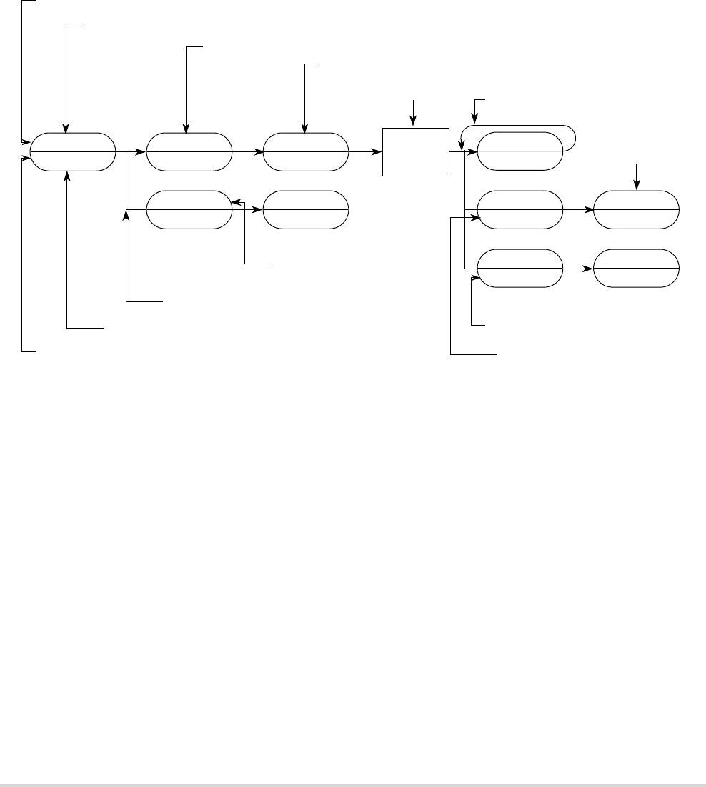
29-22 MCF5282 User’s Manual MOTOROLA
Background Debug Mode (BDM)
29.5.3.2 Command Sequence Diagrams
The command sequence diagram in Figure 29-16 shows serial bus traffic for commands.
Each bubble represents a 17-bit bus transfer. The top half of each bubble indicates the data
the development system sends to the debug module; the bottom half indicates the debug
module’s response to the previous development system commands. Command and result
transactions overlap to minimize latency.
Figure 29-16. Command Sequence Diagram
The sequence is as follows:
• In cycle 1, the development system command is issued (READ in this example). The
debug module responds with either the low-order results of the previous command
or a command complete status of the previous command, if no results are required.
• In cycle 2, the development system supplies the high-order 16 address bits. The
debug module returns a not-ready response unless the received command is decoded
as unimplemented, which is indicated by the illegal command encoding. If this
occurs, the development system should retransmit the command.
NOTE:
A not-ready response can be ignored except during a
memory-referencing cycle. Otherwise, the debug module can
accept a new serial transfer after 32 processor clock periods.
• In cycle 3, the development system supplies the low-order 16 address bits. The
debug module always returns a not-ready response.
XXX
’NOT READY’
READ (LONG)
???
MS ADDR
’NOT READY’
LS ADDR
’NOT READY’
NEXT CMD
’NOT READY’
NEXT CMD
’NOT READY’
NEXT CMD
LS RESULT
Commands transmitted to the debug module
Command code transmitted during this cycle
High-order 16 bits of memory address
Low-order 16 bits of memory address
Non-serial-related
Next
Command
Code
Sequence taken if operation
has not completed
activity
READ
MEMORY
LOCATION
XXX
BERR
XXX
MS RESULT
XXX
’ILLEGAL’
Responses from the debug module
Results from previous command
Sequence taken if illegal command
is received by debug module
Data used from this transfer
Sequence taken if bus error
occurs on memory access
High- and low-order 16 bits of result
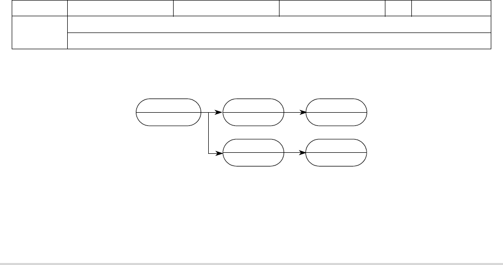
MOTOROLA Chapter 29. Debug Support 29-23
Background Debug Mode (BDM)
• At the completion of cycle 3, the debug module initiates a memory read operation.
Any serial transfers that begin during a memory access return a not-ready response.
• Results are returned in the two serial transfer cycles after the memory access
completes. For any command performing a byte-sized memory read operation, the
upper 8 bits of the response data are undefined and the referenced data is returned in
the lower 8 bits. The next command’s opcode is sent to the debug module during the
final transfer. If a memory or register access is terminated with a bus error, the error
status (S = 1, DATA = 0x0001) is returned instead of result data.
29.5.3.3 Command Set Descriptions
The following sections describe the commands summarized in Table 29-17.
NOTE:
The BDM status bit (S) is 0 for normally completed
commands; S = 1 for illegal commands, not-ready responses,
and transfers with bus-errors. Section 29.5.2, “BDM Serial
Interface,” describes the receive packet format.
Motorola reserves unassigned command opcodes for future expansion. Unused command
formats in any revision level perform a NOP and return an illegal command response.
29.5.3.3.1 Read A/D Register (RAREG/RDREG)
Read the selected address or data register and return the 32-bit result. A bus error response
is returned if the CPU core is not halted.
Command/Result Formats:
Command Sequence:
Figure 29-18. RAREG/RDREG Command Sequence
Operand Data: None
Result Data: The contents of the selected register are returned as a longword
value, most-significant word first.
15 12 11 8 7 4 3 2 0
Command 0x2 0x1 0x8 A/D Register
Result D[31:16]
D[15:0]
Figure 29-17. RAREG/RDREG Command Format
RAREG/RDREG
???
NEXT CMD
LS RESULT
NEXT CMD
’NOT READY’
XXX
BERR
XXX
MS RESULT
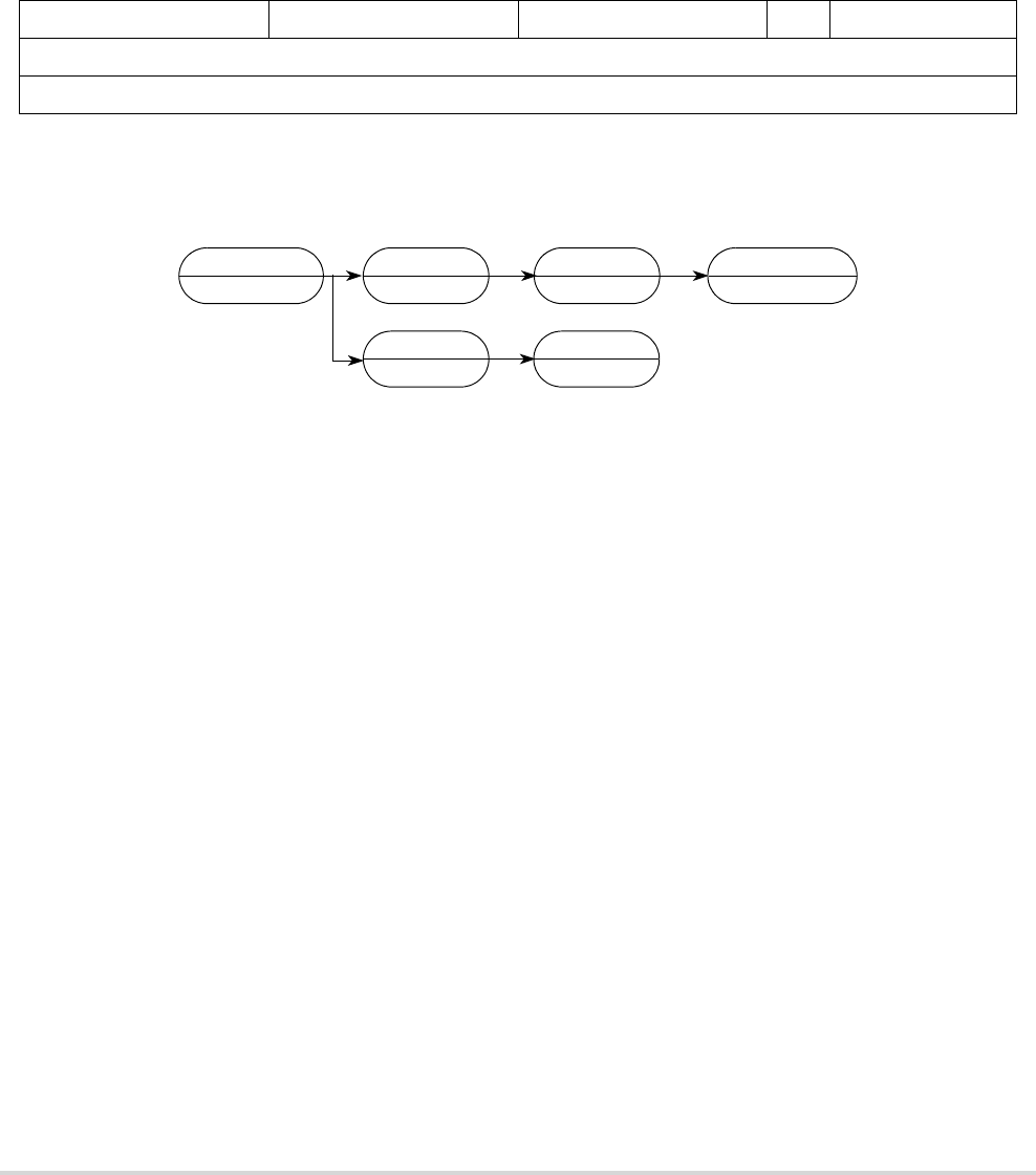
29-24 MCF5282 User’s Manual MOTOROLA
Background Debug Mode (BDM)
29.5.3.3.2 Write A/D Register (WAREG/WDREG)
The operand longword data is written to the specified address or data register. A write alters
all 32 register bits. A bus error response is returned if the CPU core is not halted.
Command Format:
Command Sequence
Figure 29-20. WAREG/WDREG Command Sequence
Operand Data Longword data is written into the specified address or data register.
The data is supplied most-significant word first.
Result Data Command complete status is indicated by returning 0xFFFF (with S
cleared) when the register write is complete.
29.5.3.3.3 Read Memory Location (READ)
Read data at the longword address. Address space is defined by BAAR[TT,TM]. Hardware
forces low-order address bits to zeros for word and longword accesses to ensure that word
addresses are word-aligned and longword addresses are longword-aligned.
15 1211 87 432 0
0x2 0x0 0x8 A/D Register
D[31:16]
D[15:0]
Figure 29-19. WAREG/WDREG Command Format
WAR E G / W D R E G
???
LS DATA
’NOT READY’
NEXT CMD
’NOT READY’
XXX
BERR
MS DATA
’NOT READY’
NEXT CMD
’CMD COMPLETE’
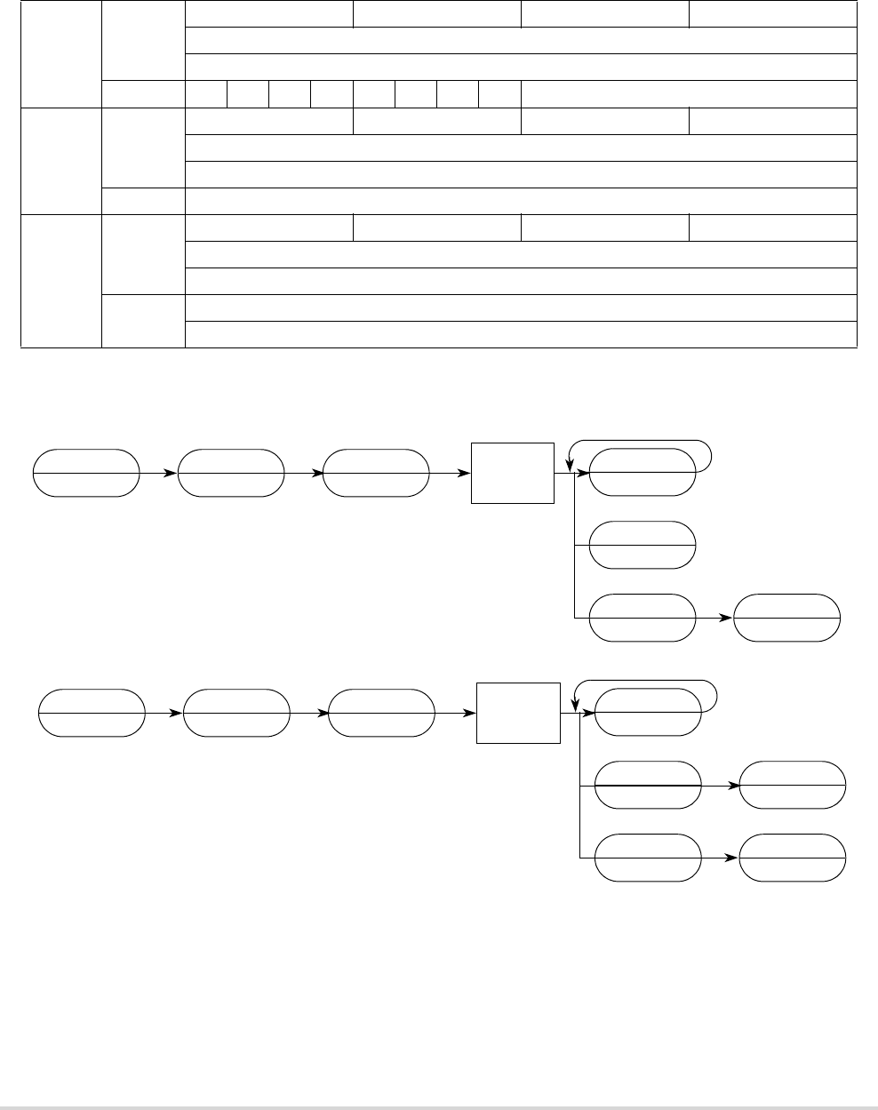
MOTOROLA Chapter 29. Debug Support 29-25
Background Debug Mode (BDM)
Command/Result Formats:
Command Sequence:
Figure 29-22. READ Command Sequence
Operand Data The only operand is the longword address of the requested location.
Result Data Word results return 16 bits of data; longword results return 32. Bytes
are returned in the LSB of a word result; the upper byte is undefined.
0x0001 (S = 1) is returned if a bus error occurs.
15 12 11 8 7 4 3 0
Byte Command 0x1 0x9 0x0 0x0
A[31:16]
A[15:0]
Result XXXXXXXX D[7:0]
Word Command 0x1 0x9 0x4 0x0
A[31:16]
A[15:0]
Result D[15:0]
Longword Command 0x1 0x9 0x8 0x0
A[31:16]
A[15:0]
Result D[31:16]
D[15:0]
Figure 29-21. READ Command/Result Formats
XXX
’NOT READY’
READ (LONG)
???
MS ADDR
’NOT READY’
LS ADDR
’NOT READY’
NEXT CMD
’NOT READY’
NEXT CMD
LS RESULT
READ
MEMORY
LOCATION
XXX
BERR
XXX
MS RESULT
XXX
’NOT READY’
READ (B/W)
???
MS ADDR
’NOT READY’
LS ADDR
’NOT READY’
NEXT CMD
’NOT READY’
READ
MEMORY
LOCATION
XXX
BERR
NEXT CMD
RESULT

29-26 MCF5282 User’s Manual MOTOROLA
Background Debug Mode (BDM)
29.5.3.3.4 Write Memory Location (WRITE)
Write data to the memory location specified by the longword address. The address space is
defined by BAAR[TT,TM]. Hardware forces low-order address bits to zeros for word and
longword accesses to ensure that word addresses are word-aligned and longword addresses
are longword-aligned.
Command Formats:
15 12 11 8 7 4 3 1
Byte 0x1 0x8 0x0 0x0
A[31:16]
A[15:0]
XXXXXXXX D[7:0]
Word 0x1 0x8 0x4 0x0
A[31:16]
A[15:0]
D[15:0]
Longword 0x1 0x8 0x8 0x0
A[31:16]
A[15:0]
D[31:16]
D[15:0]
Figure 29-23. WRITE Command Format
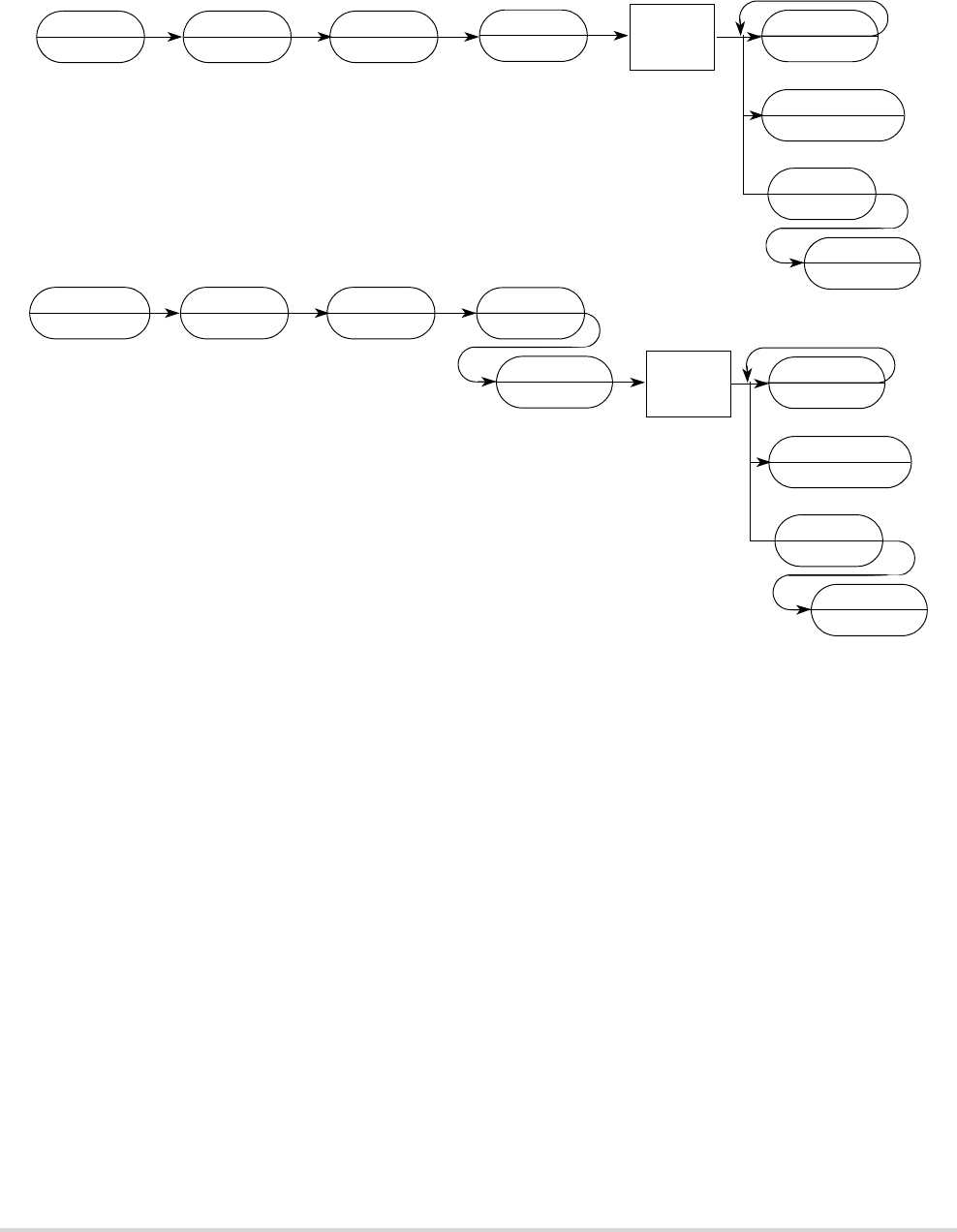
MOTOROLA Chapter 29. Debug Support 29-27
Background Debug Mode (BDM)
Command Sequence:
Figure 29-24. WRITE Command Sequence
Operand Data This two-operand instruction requires a longword absolute address
that specifies a location to which the data operand is to be written.
Byte data is sent as a 16-bit word, justified in the LSB; 16- and 32-bit
operands are sent as 16 and 32 bits, respectively
Result Data Command complete status is indicated by returning 0xFFFF (with S
cleared) when the register write is complete. A value of 0x0001 (with
S set) is returned if a bus error occurs.
29.5.3.3.5 Dump Memory Block (DUMP)
DUMP is used with the READ command to access large blocks of memory. An initial READ
is executed to set up the starting address of the block and to retrieve the first result. If an
initial READ is not executed before the first DUMP, an illegal command response is returned.
The DUMP command retrieves subsequent operands. The initial address is incremented by
the operand size (1, 2, or 4) and saved in a temporary register. Subsequent DUMP commands
use this address, perform the memory read, increment it by the current operand size, and
store the updated address in the temporary register.
XXX
’NOT READY’
WRITE (LONG)
???
MS ADDR
’NOT READY’
LS ADDR
’NOT READY’
WRITE
MEMORY
LOCATION
NEXT CMD
’CMD COMPLETE’
MS DATA
’NOT READY’
NEXT CMD
’NOT READY’
XXX
BERR
XXX
’NOT READY’
WRITE (B/W)
???
MS ADDR
’NOT READY’
LS ADDR
’NOT READY’
WRITE
MEMORY
LOCATION
NEXT CMD
’CMD COMPLETE’
DATA
’NOT READY’
NEXT CMD
’NOT READY’
XXX
BERR
LS DATA
’NOT READY’
29-28 MCF5282 User’s Manual MOTOROLA
Background Debug Mode (BDM)
NOTE:
DUMP does not check for a valid address; it is a valid command
only when preceded by NOP, READ, or another DUMP command.
Otherwise, an illegal command response is returned. NOP can
be used for intercommand padding without corrupting the
address pointer.
The size field is examined each time a DUMP command is processed, allowing the operand
size to be dynamically altered.
Command/Result Formats:
15 12 11 8 7 4 3 0
Byte Command 0x1 0xD 0x0 0x0
Result XXXXXXXX D[7:0]
Word Command 0x1 0xD 0x4 0x0
Result D[15:0]
Longword Command 0x1 0xD 0x8 0x0
Result D[31:16]
D[15:0]
Figure 29-25. DUMP Command/Result Formats
MOTOROLA Chapter 29. Debug Support 29-29
Background Debug Mode (BDM)
Command Sequence:
Figure 29-26. DUMP Command Sequence
Operand Data: None
Result Data: Requested data is returned as either a word or longword. Byte data is
returned in the least-significant byte of a word result. Word results
return 16 bits of significant data; longword results return 32 bits. A
value of 0x0001 (with S set) is returned if a bus error occurs.
29.5.3.3.6 Fill Memory Block (FILL)
A FILL command is used with the WRITE command to access large blocks of memory. An
initial WRITE is executed to set up the starting address of the block and to supply the first
operand. The FILL command writes subsequent operands. The initial address is incremented
by the operand size (1, 2, or 4) and saved in a temporary register after the memory write.
Subsequent FILL commands use this address, perform the write, increment it by the current
operand size, and store the updated address in the temporary register.
If an initial WRITE is not executed preceding the first FILL command, the illegal command
response is returned.
NOTE:
The FILL command does not check for a valid address—FILL is
a valid command only when preceded by another FILL, a NOP,
or a WRITE command. Otherwise, an illegal command response
is returned. The NOP command can be used for intercommand
padding without corrupting the address pointer.
XXX
’NOT READY’
DUMP (B/W)
???
XXX
’ILLEGAL’
NEXT CMD
’NOT READY’
NEXT CMD
’NOT READY’
READ
MEMORY
LOCATION
XXX
BERR
NEXT CMD
RESULT
XXX
’NOT READY’
DUMP (LONG)
???
XXX
’ILLEGAL’
NEXT CMD
’NOT READY’
NEXT CMD
’NOT READY’
READ
MEMORY
LOCATION
XXX
BERR
NEXT CMD
MS RESULT
NEXT CMD
LS RESULT
29-30 MCF5282 User’s Manual MOTOROLA
Background Debug Mode (BDM)
The size field is examined each time a FILL command is processed, allowing the operand
size to be altered dynamically.
Command Formats:
Command Sequence:
Figure 29-28. FILL Command Sequence
Operand Data: A single operand is data to be written to the memory location. Byte
data is sent as a 16-bit word, justified in the least-significant byte; 16-
and 32-bit operands are sent as 16 and 32 bits, respectively.
Result Data: Command complete status (0xFFFF) is returned when the register
write is complete. A value of 0x0001 (with S set) is returned if a bus
error occurs.
15 12 11 8 7 4 3 0
Byte 0x1 0xC 0x0 0x0
XXXXXXXX D[7:0]
Word 0x1 0xC 0x4 0x0
D[15:0]
Longword 0x1 0xC 0x8 0x0
D[31:16]
D[15:0]
Figure 29-27. FILL Command Format
XXX
’NOT READY’
FILL (B/W)
???
DATA
’NOT READY’
NEXT CMD
’NOT READY’
WRITE
MEMORY
LOCATION
XXX
BERR
NEXT CMD
’CMD COMPLETE’
XXX
’ILLEGAL’
NEXT CMD
’NOT READY’
XXX
’NOT READY’
FILL (LONG)
???
MS DATA
’NOT READY’
LS DATA
’NOT READY’
WRITE
MEMORY
LOCATION
XXX
BERR
NEXT CMD
’CMD COMPLETE’
XXX
’ILLEGAL’
NEXT CMD
’NOT READY’
NEXT CMD
’NOT READY’

MOTOROLA Chapter 29. Debug Support 29-31
Background Debug Mode (BDM)
29.5.3.3.7 Resume Execution (GO)
The pipeline is flushed and refilled before normal instruction execution resumes.
Prefetching begins at the current address in the PC and at the current privilege level. If any
register (such as the PC or SR) is altered by a BDM command while the processor is halted,
the updated value is used when prefetching resumes. If a GO command is issued and the
CPU is not halted, the command is ignored.
Command Sequence:
Figure 29-30. GO Command Sequence
Operand Data: None
Result Data: The command-complete response (0xFFFF) is returned during the
next shift operation.
29.5.3.3.8 No Operation (NOP)
NOP performs no operation and may be used as a null command where required.
Command Formats:
Command Sequence:
Figure 29-32. NOP Command Sequence
Operand Data: None
Result Data: The command-complete response, 0xFFFF (with S cleared), is
returned during the next shift operation.
15 12 11 8 7 4 3 0
0x0 0xC 0x0 0x0
Figure 29-29. GO Command Format
15 12 11 8 7 4 3 0
0x0 0x0 0x0 0x0
Figure 29-31. NOP Command Format
GO
???
NEXT CMD
’CMD COMPLETE’
NOP
???
NEXT CMD
’CMD COMPLETE’

29-32 MCF5282 User’s Manual MOTOROLA
Background Debug Mode (BDM)
29.5.3.3.9 Read Control Register (RCREG)
Reads the selected control register and returns the 32-bit result. Accesses to the
processor/memory control registers are always 32 bits wide, regardless of register width.
The second and third words of the command form a 32-bit address, which the debug
module uses to generate a special bus cycle to access the specified control register. The
12-bit Rc field is the same as that used by the MOVEC instruction.
Command/Result Formats:
Rc encoding:
15 12 11 8 7 4 3 0
Command 0x2 0x9 0x8 0x0
0x0 0x0 0x0 0x0
0x0 Rc
Result D[31:16]
D[15:0]
Figure 29-33. RCREG Command/Result Formats
Table 29-19. Control Register Map
Rc Register Definition
0x002 Cache Control Register (CACR)
0x004 Access Control Register (ACR0)
0x005 Access Control Register (ACR1)
0x800 Other Stack Pointer (OTHER_A7)
0x801 Vector Base Register (VBR)
0x804 MAC Status Register (MACSR)
0x805 MAC Mask Register (MASK)
0x806 MAC Accumulator 0 (ACC0)
0x807 MAC Accumulator 0,1 Extension Bytes (ACCEXT01)
0x808 MAC Accumulator 2,3 Extension Bytes (ACCEXT23)
0x809 MAC Accumulator 1 (ACC1)
0x80A MAC Accumulator 2 (ACC2)
0x80B MAC Accumulator 3 (ACC3)
0x80E Status Register (SR)
0x80F Program Register (PC)
0xC04 Flash Base Address Register 0 (FLASHBAR)
0xC05 RAM Base Address Register (RAMBAR)

MOTOROLA Chapter 29. Debug Support 29-33
Background Debug Mode (BDM)
Command Sequence:
Figure 29-34. RCREG Command Sequence
Operand Data: The only operand is the 32-bit Rc control register select field.
Result Data: Control register contents are returned as a longword,
most-significant word first. The implemented portion of registers
smaller than 32 bits is guaranteed correct; other bits are undefined.
BDM Accesses of the Stack Pointer Registers (A7: SSP, USP)
The V2 core of the MCF5282 supports two unique stack pointer (A7) registers: the
supervisor stack pointer (SSP) and the user stack pointer (USP). The hardware
implementation of these two programmable-visible 32-bit registers does not uniquely
identify one as the SSP and the other as the USP. Rather, the hardware uses one 32-bit
register as the currently-active A7 and the other register is named simply the “other_A7”.
Thus, the contents of the two hardware registers is a function of the operating mode of the
processor:
if SR[S] = 1
then A7 = Supervisor Stack Pointer
other_A7 = User Stack Pointer
else A7 = User Stack Pointer
other_A7 = Supervisor Stack Pointer
The BDM programming model supports reads and writes to the A7 and other_A7 registers
directly. It is the responsibility of the external development system to determine the
mapping of the two hardware registers (A7, other_A7) to the two program-visible
definitions (supervisor and user stack pointers), based on the Supervisor bit of the status
register.
BDM Accesses of the EMAC Registers
The presence of rounding logic in the output datapath of the EMAC requires that special
care be taken during any BDM-initiated reads and writes of its programming model. In
particular, it is necessary that any result rounding modes be disabled during the read/write
process so the exact bit-wise contents of the EMAC registers are accessed.
XXX
’NOT READY’
RCREG
???
MS ADDR
’NOT READY’
MS ADDR
’NOT READY’
NEXT CMD
’NOT READY’
READ
CONTROL
REGISTER
XXX
BERR
NEXT CMD
MS RESULT
NEXT CMD
LS RESULT

29-34 MCF5282 User’s Manual MOTOROLA
Background Debug Mode (BDM)
As an example, any BDM read of an accumulator register (ACCn) must be preceded by two
commands accessing the MAC status register. Specifically, the following BDM sequence
is required:
BdmReadACCn (
rcreg macsr; // read macsr contents & save
wcreg #0,macsr; // disable all rounding modes
rcreg accn; // read the desired accumulator
wcreg #saved_data,macsr;// restore the original macsr
)
Likewise, the following BDM sequence is needed to write an accumulator register:
BdmWriteACCn (
rcreg macsr; // read macsr contents & save
wcreg #0,macsr; // disable all rounding modes
wcreg #data,accn; // write the desired accumulator
wcreg #saved_data,macsr;// restore the original macsr
)
Additionally, it is required that writes to the accumulator extension registers be performed
after the corresponding accumulators are updated. This is needed since a write to any
accumulator alters the contents of the corresponding extension register.
For more information on saving and restoring the complete EMAC programming model,
see appropriate section of the EMAC specification.
29.5.3.3.10 Write Control Register (WCREG)
The operand (longword) data is written to the specified control register. The write alters all
32 register bits.
Command/Result Formats:
15 1211 87 43 0
Command 0x2 0x8 0x8 0x0
0x0 0x0 0x0 0x0
0x0 Rc
Result D[31:16]
D[15:0]
Figure 29-35. WCREG Command/Result Formats
MOTOROLA Chapter 29. Debug Support 29-35
Background Debug Mode (BDM)
Command Sequence:
Figure 29-36. WCREG Command Sequence
Operand Data: This instruction requires two longword operands. The first selects
the register to which the operand data is to be written; the second
contains the data.
Result Data: Successful write operations return 0xFFFF. Bus errors on the write
cycle are indicated by the setting of bit 16 in the status message and
by a data pattern of 0x0001.
29.5.3.3.11 Read Debug Module Register (RDMREG)
Read the selected debug module register and return the 32-bit result. The only valid register
selection for the RDMREG command is CSR (DRc = 0x00). Note that this read of the CSR
clears CSR[FOF, TRG, HALT, BKPT]; as well as the trigger status bits (CSR[BSTAT]) if
either a level-2 breakpoint has been triggered or a level-1 breakpoint has been triggered and
no level-2 breakpoint has been enabled.
Command/Result Formats:
Table 29-20 shows the definition of DRc encoding.
15 12 11 8 7 5 4 0
Command 0x2 0xD 100 DRc
Result D[31:16]
D[15:0]
Figure 29-37. RDMREG Command/Result Formats
XXX
’NOT READY’
WCREG
???
MS ADDR
’NOT READY’
MS ADDR
’NOT READY’
WRITE
CONTROL
REGISTER
NEXT CMD
’CMD COMPLETE’
MS DATA
’NOT READY’
NEXT CMD
’NOT READY’
XXX
BERR
LS DATA
’NOT READY’
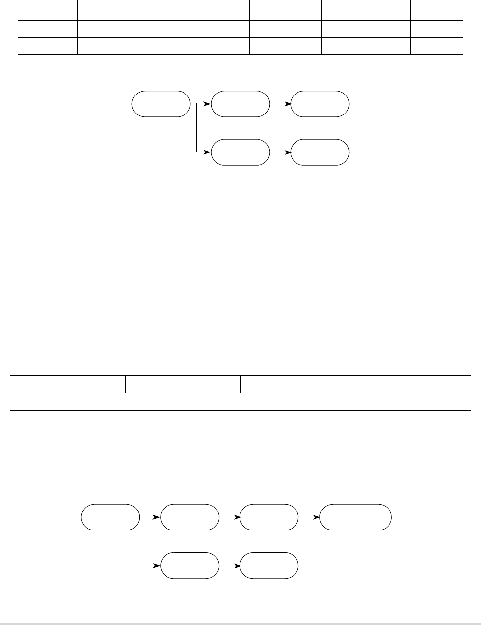
29-36 MCF5282 User’s Manual MOTOROLA
Background Debug Mode (BDM)
Command Sequence:
Figure 29-38. RDMREG Command Sequence
Operand Data: None
Result Data: The contents of the selected debug register are returned as a
longword value. The data is returned most-significant word first.
29.5.3.3.12 Write Debug Module Register (WDMREG)
The operand (longword) data is written to the specified debug module register. All 32 bits
of the register are altered by the write. DSCLK must be inactive while the debug module
register writes from the CPU accesses are performed using the WDEBUG instruction.
Command Format:
Table 29-3 shows the definition of the DRc write encoding.
Command Sequence:
Figure 29-40. WDMREG Command Sequence
Table 29-20. Definition of DRc Encoding—Read
DRc[4:0] Debug Register Definition Mnemonic Initial State Page
0x00 Configuration/Status CSR 0x0 p. 29-10
0x01–0x1F Reserved — — —
15 12 11 8 7 5 4 0
0x2 0xC 100 DRc
D[31:16]
D[15:0]
Figure 29-39. WDMREG BDM Command Format
RDMREG
???
XXX
MS RESULT
NEXT CMD
LS RESULT
XXX
’ILLEGAL’
NEXT CMD
’NOT READY’
WDMREG
???
MS DATA
’NOT READY’
LS DATA
’NOT READY’
XXX
’ILLEGAL’
NEXT CMD
’NOT READY’
NEXT CMD
’CMD COMPLETE’

MOTOROLA Chapter 29. Debug Support 29-37
Real-Time Debug Support
Operand Data: Longword data is written into the specified debug register. The data
is supplied most-significant word first.
Result Data: Command complete status (0xFFFF) is returned when register write
is complete.
29.6 Real-Time Debug Support
The ColdFire Family provides support debugging real-time applications. For these types of
embedded systems, the processor must continue to operate during debug. The foundation
of this area of debug support is that while the processor cannot be halted to allow
debugging, the system can generally tolerate small intrusions into the real-time operation.
The debug module provides three types of breakpoints—PC with mask, operand address
range, and data with mask. These breakpoints can be configured into one- or two-level
triggers with the exact trigger response also programmable. The debug module
programming model can be written from either the external development system using the
debug serial interface or from the processor’s supervisor programming model using the
WDEBUG instruction. Only CSR is readable using the external development system.
29.6.1 Theory of Operation
Breakpoint hardware can be configured to respond to triggers in several ways. The response
desired is programmed into TDR. As shown in Table 29-21, when a breakpoint is triggered,
an indication (CSR[BSTAT]) is provided on the DDATA output port when it is not
displaying captured processor status, operands, or branch addresses.
The breakpoint status is also posted in the CSR. Note that CSR[BSTAT] is cleared by a CSR
read when either a level-2 breakpoint is triggered or a level-1 breakpoint is triggered and a
level-2 breakpoint is not enabled. Status is also cleared by writing to TDR.
BDM instructions use the appropriate registers to load and configure breakpoints. As the
system operates, a breakpoint trigger generates the response defined in TDR.
PC breakpoints are treated in a precise manner—exception recognition and processing are
initiated before the excepting instruction is executed. All other breakpoint events are
Table 29-21. DDATA[3:0]/CSR[BSTAT] Breakpoint Response
DDATA[3:0]/CSR[BSTAT] 1
1Encodings not shown are reserved for future use.
Breakpoint Status
0000/0000 No breakpoints enabled
0010/0001 Waiting for level-1 breakpoint
0100/0010 Level-1 breakpoint triggered
1010/0101 Waiting for level-2 breakpoint
1100/0110 Level-2 breakpoint triggered

29-38 MCF5282 User’s Manual MOTOROLA
Real-Time Debug Support
recognized on the processor’s local bus, but are made pending to the processor and sampled
like other interrupt conditions. As a result, these interrupts are imprecise.
In systems that tolerate the processor being halted, a BDM-entry can be used. With
TDR[TRC] =01, a breakpoint trigger causes the core to halt (PST = 0xF).
If the processor core cannot be halted, the debug interrupt can be used. With this
configuration, TDR[TRC] = 10, the breakpoint trigger becomes a debug interrupt to the
processor, which is treated higher than the nonmaskable level-7 interrupt request. As with
all interrupts, it is made pending until the processor reaches a sample point, which occurs
once per instruction. Again, the hardware forces the PC breakpoint to occur before the
targeted instruction executes. This is possible because the PC breakpoint is enabled when
interrupt sampling occurs. For address and data breakpoints, reporting is considered
imprecise because several instructions may execute after the triggering address or data is
detected.
As soon as the debug interrupt is recognized, the processor aborts execution and initiates
exception processing. This event is signaled externally by the assertion of a unique PST
value (PST = 0xD) for multiple cycles. The core enters emulator mode when exception
processing begins. After the standard 8-byte exception stack is created, the processor
fetches a unique exception vector, 12, from the vector table.
Execution continues at the instruction address in the vector corresponding to the breakpoint
triggered. All interrupts are ignored while the processor is in emulator mode. The debug
interrupt handler can use supervisor instructions to save the necessary context such as the
state of all program-visible registers into a reserved memory area.
When debug interrupt operations complete, the RTE instruction executes and the processor
exits emulator mode. After the debug interrupt handler completes execution, the external
development system can use BDM commands to read the reserved memory locations.
If a hardware breakpoint such as a PC trigger is left unmodified by the debug interrupt
service routine, another debug interrupt is generated after the completion of the RTE
instruction.
29.6.1.1 Emulator Mode
Emulator mode is used to facilitate non-intrusive emulator functionality. This mode can be
entered in three different ways:
• Setting CSR[EMU] forces the processor into emulator mode. EMU is examined
only if RSTI is negated and the processor begins reset exception processing. It can
be set while the processor is halted before reset exception processing begins. See
Section 29.5.1, “CPU Halt.”
• A debug interrupt always puts the processor in emulation mode when debug
interrupt exception processing begins.

MOTOROLA Chapter 29. Debug Support 29-39
Real-Time Debug Support
• Setting CSR[TRC] forces the processor into emulation mode when trace exception
processing begins.
While operating in emulation mode, the processor exhibits the following properties:
• All interrupts are ignored, including level-7 interrupts.
• If CSR[MAP] = 1, all caching of memory and the SRAM module are disabled. All
memory accesses are forced into a specially mapped address space signaled by
TT = 0x2, TM = 0x5 or 0x6. This includes stack frame writes and the vector fetch
for the exception that forced entry into this mode.
The RTE instruction exits emulation mode. The processor status output port provides a
unique encoding for emulator mode entry (0xD) and exit (0x7).
29.6.2 Concurrent BDM and Processor Operation
The debug module supports concurrent operation of both the processor and most BDM
commands. BDM commands may be executed while the processor is running, except those
following operations that access processor/memory registers:
• Read/write address and data registers
• Read/write control registers
For BDM commands that access memory, the debug module requests the processor’s local
bus. The processor responds by stalling the instruction fetch pipeline and waiting for
current bus activity to complete before freeing the local bus for the debug module to
perform its access. After the debug module bus cycle, the processor reclaims the bus.
Breakpoint registers must be carefully configured in a development system if the processor
is executing. The debug module contains no hardware interlocks, so TDR should be
disabled while breakpoint registers are loaded, after which TDR can be written to define
the exact trigger. This prevents spurious breakpoint triggers.
Because there are no hardware interlocks in the debug unit, no BDM operations are allowed
while the CPU is writing the debug’s registers (DSCLK must be inactive).
Note that the debug module requires the use of the internal bus to perform BDM
commands. In Revision A, if the processor is executing a tight loop that is contained within
a single aligned longword, the processor may never grant the internal bus to the debug
module, for example:
align4
label1: nop
bra.b label1
or
align4
label2: bra.w label2
The processor grants the internal bus if these loops are forced across two longwords.

29-40 MCF5282 User’s Manual MOTOROLA
Processor Status, DDATA Definition
29.7 Processor Status, DDATA Definition
This section specifies the ColdFire processor and debug module’s generation of the
processor status (PST) and debug data (DDATA) output on an instruction basis. In general,
the PST/DDATA output for an instruction is defined as follows:
PST = 0x1, {PST = [0x89B], DDATA= operand}
where the {...} definition is optional operand information defined by the setting of the CSR.
The CSR provides capabilities to display operands based on reference type (read, write, or
both). A PST value {0x8, 0x9, or 0xB} identifies the size and presence of valid data to
follow on the DDATA output {1, 2, or 4 bytes}. Additionally, for certain change-of-flow
branch instructions, CSR[BTB] provides the capability to display the target instruction
address on the DDATA output {2, 3, or 4 bytes} using a PST value of {0x9, 0xA, or 0xB}.
29.7.1 User Instruction Set
Table 29-22 shows the PST/DDATA specification for user-mode instructions. Rn
represents any {Dn, An} register. In this definition, the ‘y’ suffix generally denotes the
source and ‘x’ denotes the destination operand. For a given instruction, the optional
operand data is displayed only for those effective addresses referencing memory. The ‘DD’
nomenclature refers to the DDATA outputs.
Table 29-22. PST/DDATA Specification for User-Mode Instructions
Instruction Operand Syntax PST/DDATA
add.l <ea>y,Rx PST = 0x1, {PST = 0xB, DD = source operand}
add.l Dy,<ea>x PST = 0x1, {PST = 0xB, DD = source}, {PST = 0xB, DD = destination}
addi.l #imm,Dx PST = 0x1
addq.l #imm,<ea>x PST = 0x1, {PST = 0xB, DD = source}, {PST = 0xB, DD = destination}
addx.l Dy,Dx PST = 0x1
and.l <ea>y,Dx PST = 0x1, {PST = 0xB, DD = source operand}
and.l Dy,<ea>x PST = 0x1, {PST = 0xB, DD = source}, {PST = 0xB, DD = destination}
andi.l #imm,Dx PST = 0x1
asl.l {Dy,#imm},Dx PST = 0x1
asr.l {Dy,#imm},Dx PST = 0x1
bitrev.l Dx PST = 0x1
byterev.l Dx PST = 0x1
bcc.{b,w} if taken, then PST = 0x5, else PST = 0x1
bchg #imm,<ea>x PST = 0x1, {PST = 0x8, DD = source}, {PST = 0x8, DD = destination}
bchg Dy,<ea>x PST = 0x1, {PST = 0x8, DD = source}, {PST = 0x8, DD = destination}

MOTOROLA Chapter 29. Debug Support 29-41
Processor Status, DDATA Definition
bclr #imm,<ea>x PST = 0x1, {PST = 0x8, DD = source}, {PST = 0x8, DD = destination}
bclr Dy,<ea>x PST = 0x1, {PST = 0x8, DD = source}, {PST = 0x8, DD = destination}
bra.{b,w} PST = 0x5
bset #imm,<ea>x PST = 0x1, {PST = 0x8, DD = source}, {PST = 0x8, DD = destination}
bset Dy,<ea>x PST = 0x1, {PST = 0x8, DD = source}, {PST = 0x8, DD = destination}
bsr.{b,w} PST = 0x5, {PST = 0xB, DD = destination operand}
btst #imm,<ea>x PST = 0x1, {PST = 0x8, DD = source operand}
btst Dy,<ea>x PST = 0x1, {PST = 0x8, DD = source operand}
clr.b <ea>x PST = 0x1, {PST = 0x8, DD = destination operand}
clr.l <ea>x PST = 0x1, {PST = 0xB, DD = destination operand}
clr.w <ea>x PST = 0x1, {PST = 0x9, DD = destination operand}
cmp.l <ea>y,Rx PST = 0x1, {PST = 0xB, DD = source operand}
cmpi.l #imm,Dx PST = 0x1
divs.l <ea>y,Dx PST = 0x1, {PST = 0xB, DD = source operand}
divs.w <ea>y,Dx PST = 0x1, {PST = 0x9, DD = source operand}
divu.l <ea>y,Dx PST = 0x1, {PST = 0xB, DD = source operand}
divu.w <ea>y,Dx PST = 0x1, {PST = 0x9, DD = source operand}
eor.l Dy,<ea>x PST = 0x1, {PST = 0xB, DD = source}, {PST = 0xB, DD = destination}
eori.l #imm,Dx PST = 0x1
ext.l Dx PST = 0x1
ext.w Dx PST = 0x1
extb.l Dx PST = 0x1
ff1.l Dx PST = 0x1
jmp <ea>x PST = 0x5, {PST = [0x9AB], DD = target address} 1
jsr <ea>x PST = 0x5, {PST = [0x9AB], DD = target address},
{PST = 0xB , DD = destination operand} 1
lea <ea>y,Ax PST = 0x1
link.w Ay,#imm PST = 0x1, {PST = 0xB, DD = destination operand}
lsl.l {Dy,#imm},Dx PST = 0x1
lsr.l {Dy,#imm},Dx PST = 0x1
move.b <ea>y,<ea>x PST = 0x1, {PST = 0x8, DD = source}, {PST = 0x8, DD = destination}
move.l <ea>y,<ea>x PST = 0x1, {PST = 0xB, DD = source}, {PST = 0xB, DD = destination}
move.w <ea>y,<ea>x PST = 0x1, {PST = 0x9, DD = source}, {PST = 0x9, DD = destination}
move.w CCR,Dx PST = 0x1
Table 29-22. PST/DDATA Specification for User-Mode Instructions (continued)
Instruction Operand Syntax PST/DDATA

29-42 MCF5282 User’s Manual MOTOROLA
Processor Status, DDATA Definition
move.w {Dy,#imm},CCR PST = 0x1
movem.l #list,<ea>x PST = 0x1, {PST = 0xB, DD = destination},... 2
movem.l <ea>y,#list PST = 0x1, {PST = 0xB, DD = source},... 2
moveq #imm,Dx PST = 0x1
muls.l <ea>y,Dx PST = 0x1, {PST = 0xB, DD = source operand}
muls.w <ea>y,Dx PST = 0x1, {PST = 0x9, DD = source operand}
mulu.l <ea>y,Dx PST = 0x1, {PST = 0xB, DD = source operand}
mulu.w <ea>y,Dx PST = 0x1, {PST = 0x9, DD = source operand}
neg.l Dx PST = 0x1
negx.l Dx PST = 0x1
nop PST = 0x1
not.l Dx PST = 0x1
or.l <ea>y,Dx PST = 0x1, {PST = 0xB, DD = source operand}
or.l Dy,<ea>x PST = 0x1, {PST = 0xB, DD = source}, {PST = 0xB, DD = destination}
ori.l #imm,Dx PST = 0x1
pea <ea>y PST = 0x1, {PST = 0xB, DD = destination operand}
pulse PST = 0x4
rems.l <ea>y,Dx:Dw PST = 0x1, {PST = 0xB, DD = source operand}
remu.l <ea>y,Dx:Dw PST = 0x1, {PST = 0xB, DD = source operand}
rts PST = 0x1, {PST = 0xB, DD = source operand},
PST = 0x5, {PST = [0x9AB], DD = target address}
scc Dx PST = 0x1
sub.l <ea>y,Rx PST = 0x1, {PST = 0xB, DD = source operand}
sub.l Dy,<ea>x PST = 0x1, {PST = 0xB, DD = source}, {PST = 0xB, DD = destination}
subi.l #imm,Dx PST = 0x1
subq.l #imm,<ea>x PST = 0x1, {PST = 0xB, DD = source}, {PST = 0xB, DD = destination}
subx.l Dy,Dx PST = 0x1
swap Dx PST = 0x1
trap #imm PST = 0x1 3
trapf PST = 0x1
tst.b <ea>x PST = 0x1, {PST = 0x8, DD = source operand}
tst.l <ea>x PST = 0x1, {PST = 0xB, DD = source operand}
tst.w <ea>x PST = 0x1, {PST = 0x9, DD = source operand}
unlk Ax PST = 0x1, {PST = 0xB, DD = destination operand}
Table 29-22. PST/DDATA Specification for User-Mode Instructions (continued)
Instruction Operand Syntax PST/DDATA

MOTOROLA Chapter 29. Debug Support 29-43
Processor Status, DDATA Definition
Exception Processing PST = 0xC, {PST = 0xB,DD = destination}, // stack frame
{PST = 0xB,DD = destination}, // stack frame
{PST = 0xB,DD = source}, // vector read
PST = 0x5, {PST = [0x9AB],DD = target} // handler PC
The PST/DDATA specification for the reset exception is shown below:
Exception Processing PST = 0xC,
PST = 0x5, {PST = [0x9AB],DD = target} // handler PC
The initial references at address 0 and 4 are never captured nor displayed since these
accesses are treated as instruction fetches.
For all types of exception processing, the PST = 0xC value is driven at all times, unless the
PST output is needed for one of the optional marker values or for the taken branch indicator
(0x5).
Table 29-23 shows the PST/DDATA specification for multiply-accumulate instructions.
wddata.b <ea>y PST = 0x4, {PST = 0x8, DD = source operand
wddata.l <ea>y PST = 0x4, {PST = 0xB, DD = source operand
wddata.w <ea>y PST = 0x4, {PST = 0x9, DD = source operand
1For JMP and JSR instructions, the optional target instruction address is displayed only for those effective address fields
defining variant addressing modes. This includes the following <ea>x values: (An), (d16,An), (d8,An,Xi), (d8,PC,Xi).
2For Move Multiple instructions (MOVEM), the processor automatically generates line-sized transfers if the operand
address reaches a 0-modulo-16 boundary and there are four or more registers to be transferred. For these line-sized
transfers, the operand data is never captured nor displayed, regardless of the CSR value.
The automatic line-sized burst transfers are provided to maximize performance during these sequential memory access
operations.
3During normal exception processing, the PST output is driven to a 0xC indicating the exception processing state. The
exception stack write operands, as well as the vector read and target address of the exception handler may also be
displayed.
Table 29-23. PST/DDATA Specification for MAC Instructions
Instruction Operand Syntax PST/DDATA
mac.l Ry,Rx,Accx PST = 0x1
mac.l RyRx,<ea>,Rw,Accx PST = 0x1, {PST = 0xB, DD = source operand}
mac.w Ry,Rx,Accx PST = 0x1
mac.w Ry,Rx,<ea>,Rw,Accx PST = 0x1, {PST = 0xB, DD = source operand}
move.l <ea>y,Accx PST = 0x1
move.l Accy,Accx PST = 0x1
move.l <ea>y,MACR PST = 0x1
move.l <ea>y,MASK PST = 0x1
move.l <ea>y,Accext01 PST = 0x1
move.l <ea>y,Accext23 PST = 0x1
Table 29-22. PST/DDATA Specification for User-Mode Instructions (continued)
Instruction Operand Syntax PST/DDATA

29-44 MCF5282 User’s Manual MOTOROLA
Processor Status, DDATA Definition
29.7.2 Supervisor Instruction Set
The supervisor instruction set has complete access to the user mode instructions plus the
opcodes shown below. The PST/DDATA specification for these opcodes is shown in
Table 29-24.
The move-to-SR, STLDSR, and RTE instructions include an optional PST = 0x3 value,
indicating an entry into user mode. Additionally, if the execution of a RTE instruction
returns the processor to emulator mode, a multiple-cycle status of 0xD is signaled.
Similar to the exception processing mode, the stopped state (PST = 0xE) and the halted
state (PST = 0xF) display this status throughout the entire time the ColdFire processor is in
the given mode.
move.l Accy,Rx PST = 0x1
move.l MACSR,CCR PST = 0x1
move.l MACSR,Rx PST = 0x1
move.l MASK,Rx PST = 0x1
move.l Accext01,Rx PST = 0x1
move.l Accext23,Rx PST = 0x1
msac.l Ry,Rx,Accx PST = 0x1
msac.l Ry,Rx,<ea>,Rw,Accx PST = 0x1, {PST = 0xB, DD = source operand}
msac.w Ry,Rx,Accx PST = 0x1
msac.w Ry,Rx,<ea>,Rw,Accx PST = 0x1, {PST = 0xB, DD = source operand}
Table 29-24. PST/DDATA Specification for Supervisor-Mode Instructions
Instruction Operand Syntax PST/DDATA
cpushl PST = 0x1
halt PST = 0x1,
PST = 0xF
move.w SR,Dx PST = 0x1
move.w {Dy,#imm},SR PST = 0x1, {PST = 0x3}
movec Ry,Rc PST = 0x1
rte PST = 0x7, {PST = 0xB, DD = source operand}, {PST = 3}, { PST =0xB,
DD =source operand},
PST = 0x5, {[PST = 0x9AB], DD = target address}
stldsr.w #imm PST = 0x1, {PST = 0xA, DD = destination operand, PST = 0x3}
stop #imm PST = 0x1,
PST = 0xE
wdebug <ea>y PST = 0x1, {PST = 0xB, DD = source, PST = 0xB, DD = source}
Table 29-23. PST/DDATA Specification for MAC Instructions (continued)
Instruction Operand Syntax PST/DDATA
MOTOROLA Chapter 29. Debug Support 29-45
Motorola-Recommended BDM Pinout
29.8 Motorola-Recommended BDM Pinout
The ColdFire BDM connector, Figure 29-41, is a 26-pin Berg connector arranged 2 x 13.
Figure 29-41. Recommended BDM Connector
1
3
5
7
9
11
13
15
17
19
21
23
25
2
4
6
8
10
12
14
16
18
20
22
24
26
Developer reserved 1
GND
GND
RESET
Pad-Voltage2
GND
PST2
PST0
DDATA2
DDATA0
Motorola reserved
GND
Core-Voltage
BKPT
DSCLK
Developer reserved 1
DSI
DSO
PST3
PST1
DDATA3
DDATA1
GND
Motorola reserved
CLKOUT
2Supplied by target
1Pins reserved for BDM developer use.
TA

29-46 MCF5282 User’s Manual MOTOROLA
Motorola-Recommended BDM Pinout

MOTOROLA Chapter 30. Chip Configuration Module (CCM) 30-1
Chapter 30
Chip Configuration Module (CCM)
The chip configuration module (CCM) controls the chip configuration and mode of
operation for the MCF5282.
30.1 Features
The CCM performs these operations.
• Selects the chip operating mode:
— Master mode
— Single-chip mode
• Selects external clock or phase-lock loop (PLL) mode with internal or external
reference
• Selects output pad drive strength
• Selects boot device and data port size
• Selects bus monitor configuration
• Selects low-power configuration
• Selects transfer size function of the external bus
• Selects processor status (PSTAT) and processor debug data (DDATA) functions
• Selects BDM or JTAG mode
30.2 Modes of Operation
The CCM configures the chip for two modes of operation:
• Master mode
• Single-chip mode
The operating mode is determined at reset and cannot be changed thereafter.

30-2 MCF5282 User’s Manual MOTOROLA
Block Diagram
30.2.1 Master Mode
In master mode, the central processor unit (CPU) can access external memories and
peripherals. The external bus consists of a 32-bit data bus and 24 address lines. The
available bus control signals include R/W, TS, TIP, TSIZ[1:0], TA, TEA, OE, and BS[3:0].
Up to seven chip selects can be programmed to select and control external devices and to
provide bus cycle termination. When interfacing to 16-bit ports, the port C and D pins and
PJ[5:4] (BS[1:0]) can be configured as general-purpose input/output (I/O), and when
interfacing to 8-bit ports, the ports B, C and D pins and PJ[7:5] (BS[3:1]) can be configured
as general purpose input/output (I/O).
30.2.2 Single-Chip Mode
In single-chip mode, all memory is internal to the chip. All external bus pins are configured
as general purpose I/O.
30.3 Block Diagram
Figure 30-1. Chip Configuration Module Block Diagram
Reset
Chip Mode
Selection
Boot Device / Port
Size Selection
Output Pad
Strength Selection
Clock Mode
Selection
Chip Select
Configuration
Configuration
Reset Configuration Register
Chip Configuration Register
Chip Identification Register
Chip Test Register

MOTOROLA Chapter 30. Chip Configuration Module (CCM) 30-3
Signal Descriptions
30.4 Signal Descriptions
Table 30-1 provides an overview of the CCM signals.
30.4.1 RCON
If the external RCON pin is asserted during reset, then various chip functions, including the
reset configuration pin functions after reset, are configured according to the levels driven
onto the external data pins. (see Section 30.6, “Functional Description”). The internal
configuration signals are driven to reflect the levels on the external configuration pins to
allow for module configuration.
30.4.2 CLKMOD[1:0]
The state of the CLKMOD[1:0] pins during reset determines the clock mode after reset.
30.4.3 D[26:24, 21, 19:16] (Reset Configuration Override)
If the external RCON pin is asserted during reset, then the states of these data pins during
reset determine the chip mode of operation, boot device, clock mode, and certain module
configurations after reset.
30.5 Memory Map and Registers
This subsection provides a description of the memory map and registers.
30.5.1 Programming Model
The CCM programming model consists of these registers:
• The chip configuration register (CCR) controls the main chip configuration.
• The reset configuration register (RCON) indicates the default chip configuration.
• The chip identification register (CIR) contains a unique part number.
Table 30-1. Signal Properties
Name Function Reset State
RCON Reset configuration select Internal weak
pull-up device
CLKMOD[1:0] Clock mode select —
D[26:24, 21, 19:16] Reset configuration override pins —
30-4 MCF5282 User’s Manual MOTOROLA
Memory Map and Registers
Some control register bits are implemented as write-once bits. These bits are always
readable, but once the bit has been written, additional writes have no effect, except during
debug and test operations.
Some write-once bits can be read and written while in debug mode. When debug mode is
exited, the chip configuration module resumes operation based on the current register
values. If a write to a write-once register bit occurs while in debug mode, the register bit
remains writable on exit from debug or test mode. Table 30-2 shows the accessibility of
write-once bits.
30.5.2 Memory Map
Table 30-2. Write-Once Bits Read/Write Accessibility
Configuration Read/Write Access
All configurations Read-always
Debug operation (all modes) Write-always
Master mode Write-once
Single-chip mode Write-once
Table 30-3. Chip Configuration Module Memory Map
IPSBAR Offset Bits 31–16 Bits 15–0 Access 1
1S = CPU supervisor mode access only. User mode accesses to supervisor only addresses have no effect and result in a cycle termination
transfer error.
0x0011_0004 Chip Configuration Register (CCR) Low-Power Control Register (LPCR) 2
2See Chapter 7, “Power Management,” for a description of the LPCR. It is shown here only to warn against accidental writes to this register.
S
0x0011_0008 Reset Configuration Register (RCON) Chip Identification Register (CIR) S
0x0011_000c Reserved 3
3Writing to reserved addresses with values other than 0 could put the device in a test mode; reading returns 0s.
S
0x0011_0010 Unimplemented 4
4Accessing an unimplemented address has no effect and causes a cycle termination transfer error.
NOTE
To safeguard against unintentionally activating test logic, write
0x0000 to the above reserved location during initialization
(immediately after reset) to lock out test features. Setting any bits in
the CCR may lead to unpredictable results.
—

MOTOROLA Chapter 30. Chip Configuration Module (CCM) 30-5
Memory Map and Registers
30.5.3 Register Descriptions
The following subsection describes the CCM registers.
30.5.3.1 Chip Configuration Register (CCR)
15 14 11 10 8 7 6 5 4 3 2 0
Field LOAD — MODE — SZEN PSTEN — BME BMT
Reset See Note
R/W R/W Read Only R/W
Address IPSBAR + 0x11_0004
Note: The reset value of the LOAD and MODE fields is determined during reset configuration. The SZEN is set for
master mode and cleared for all other configurations. The BME bit is set to enable the bus monitor and all other bits in
the register are cleared at reset.
Figure 30-2. Chip Configuration Register (CCR)
Table 30-4. CCR Field Descriptions
Bits Name Description
15 LOAD Pad driver load. The LOAD bit selects full or partial drive strength for selected pad output drivers. For
maximum capacitive load, set the LOAD bit to select full drive strength. For reduced power consumption
and reduced electromagnetic interference (EMI), clear the LOAD bit to select partial drive strength.
0 Default drive strength.
1 Full drive strength.
Table 30-2 shows the read/write accessibility of this write-once bit.
14–11 — Reserved, should be cleared.
10–8 MODE Chip configuration mode. This read-only field reflects the chip configuration mode.
000-101 Reserved.
110 Single-chip mode.
111 Master mode.
7 — Reserved, should be cleared.
6 SZEN SIZ[1:0] enable. This read/write bit enables the SIZ[1:0] function of the external pins.
0 SIZ[1:0] function disabled.
1 SIZ[1:0] function enabled.
5 PSTEN PST[3:0]/DDATA[3:0] enable. This read/write bit enables the Processor Status (PST) and Debug Data
(DDATA)n functions of the external pins.
0 PST/DDATA function disabled.
1 PST/DDATA function enabled.
4 — Reserved, should be cleared.

30-6 MCF5282 User’s Manual MOTOROLA
Memory Map and Registers
30.5.3.2 Reset Configuration Register (RCON)
At reset, RCON determines the default operation of certain chip functions. All default
functions defined by the RCON values can only be overridden during reset configuration
(see Section 30.6.1, “Reset Configuration”) if the external RCON pin is asserted. RCON is
a read-only register.
3 BME Bus monitor enable. This read/write bit enables the bus monitor to operate during external bus cycles.
0 Bus monitor disabled for external bus cycles.
1 Bus monitor enabled for external bus cycles.
Table 30-2 shows the read/write accessibility of this write-once bit.
2–0 BMT Bus monitor timing. This field selects the timeout period (in system clocks) for the bus monitor.
000 65536
001 32768
010 16384
011 8192
100 4096
101 2048
110 1024
111 512
Table 30-2 shows the read/write accessibility of this write-once bit.
15 10 9 8 7 6 5 4 3 2 1 0
Field — RCSC RPLLSEL RPLLREF RLOAD BOOTPS BOOTSEL — MODE
Reset 0000_0000_1110_0000
R/W R
Address IPSBAR + 0x11_0008
Figure 30-3. Reset Configuration Register (RCON)
Table 30-5. RCON Field Descriptions
Bits Name Description
15–10 — Reserved, should be cleared.
9–8 RCSC Chip select configuration. Reflects the default chip select configuration. The default function of the
chip select configuration can be overridden during reset configuration. See Table 30-6 for bit
encodings.
7 RPLLSEL PLL mode select. Reflects the default PLL mode.
0 1:1 PLL mode
1 Normal PLL mode (This is the value used for the MCF5282.)
The default PLL mode can be overridden during reset configuration. If the default is overridden, the
clock module’s SYNSR[PLLSEL] bit reflects the PLL mode.
Table 30-4. CCR Field Descriptions (continued)
Bits Name Description

MOTOROLA Chapter 30. Chip Configuration Module (CCM) 30-7
Memory Map and Registers
Table 30-6. RCSC Chip Select Configuration
Table 30-7. BOOTPS Port Size Configuration
6 RPLLREF PLL reference. Reflects the default PLL reference when the PLL is enabled in normal PLL mode.
0 External clock is PLL reference
1 Crystal oscillator is PLL reference (This is the value used for the MCF5282.)
The default PLL reference can be overridden during reset configuration. If the default is overridden,
the clock module’s SYNSR[PLLREF] reflects the PLL reference.
5 RLOAD Pad driver load. Reflects the default pad driver strength configuration.
0 Partial drive strength
1 Full drive strength (This is the value used for the MCF5282.)
4–3 BOOTPS Boot port size. Reflects the default selection for the boot port size if the boot device is configured to be
external. Table 30-7 shows the different port configurations for BOOTPS. The default function of the
boot port size can be overridden during reset configuration.
2 BOOTSEL Boot select. Reflects the default selection for the boot device.
0 Boot from internal boot device (This is the value used for the MCF5282.)
1 Boot from external boot device
1 — Reserved, should be cleared.
0 MODE Chip configuration mode. Reflects the default chip configuration mode.
0 Single-chip mode (This is the value used for the MCF5282.)
1 Master mode
The default mode can be overridden during reset configuration. If the default is overridden, the
CCR[MODE0] reflects the mode configuration.
RCSC Chip Select Configuration
00 1
1This is the value used for the MCF5282.
PF[7:5] = A[23:21]
01 PF[7] = CS6 / PF[6:5] = A[22:21]
10 PF[7:6] = CS6, CS5 / PF[5] = A[21]
11 PF[7:5] = CS6, CS5, CS4
BOOTPS[1:0] Boot Port Size
00 1
1This is the value used for the MCF5282.
Internal (32 bits)
01 16 bits
10 8 bits
11 32 bits
Table 30-5. RCON Field Descriptions (continued)
Bits Name Description

30-8 MCF5282 User’s Manual MOTOROLA
Functional Description
30.5.3.3 Chip Identification Register (CIR)
30.6 Functional Description
Six functions are defined within the chip configuration module:
1. Reset configuration
2. Chip mode selection
3. Boot device selection
4. Output pad strength configuration
5. Clock mode selections
6. Chip select configuration
These functions are described here.
30.6.1 Reset Configuration
During reset, the pins for the reset override functions are immediately configured to known
states. Table 30-9 shows the states of the external pins while in reset.
15 8 7 0
Field PIN PRN
Reset 0010_0000_0000_0000
R/W R
Address IPSBAR + 0x11_000a
Figure 30-4. Chip Identification Register (CIR)
Table 30-8. CIR Field Description
Bits Name Description
15–8 PIN Part identification number. Contains a unique identification number for the device.
7–0 PRN Part revision number. This number is increased by one for each new full-layer mask
set of this part. The revision numbers are assigned in chronological order.

MOTOROLA Chapter 30. Chip Configuration Module (CCM) 30-9
Functional Description
If the RCON pin is not asserted during reset, the chip configuration and the reset
configuration pin functions after reset are determined by RCON or fixed defaults,
regardless of the states of the external data pins. The internal configuration signals are
driven to levels specified by the RCON register’s reset state for default module
configuration.
If the RCON pin is asserted during reset, then various chip functions, including the reset
configuration pin functions after reset, are configured according to the levels driven onto
the external data pins. (See Table 30-10) The internal configuration signals are driven to
reflect the levels on the external configuration pins to allow for module configuration.
Table 30-9. Reset Configuration Pin States During Reset
Pin Pin
Function 1
1If the external RCON pin is not asserted during reset, pin functions are determined by the default
operation mode defined in the RCON register. If the external RCON pin is asserted, pin functions are
determined by the override values driven on the external data bus pins.
I/O Output
State
Input
State
D[26:24, 21, 19:16],
PA[2:0], PB[5, 3:0]
Digital I/O or primary
function
Input — Must be driven
by external logic
RCON RCON function for all
modes 2
2During reset, the external RCON pin assumes its RCON pin function, but this pin changes to the
function defined by the chip operation mode immediately after reset. See Table 30-10.
Input — Internal weak pull-up
device
CLKMOD1, CLKMOD0 Not affected Input — Must be driven by
external logic
Table 30-10. Configuration During Reset 1
Pin(s) Affected Default
Configuration
Override Pins
in Reset 2, 3 4 Function
D[31:0], R/W, TA, TEA,
TSIZ[1:0], TS, TIP, OE, A[23:0],
BS[3:0], CS[3:0]
RCON0 = 0 D[26,17:16] Chip Mode Selected
111 Master mode
110 Single-chip mode 5
100 or 0XX Reserved
CS0 RCON[4:3] = 00
RCON2 = 0
D[19:18] Boot Device
00 Internal with 32-bit port5
10 External with 8-bit port
01 External with 16-bit port
11 External with 32-bit port
All output pins RCON5 = 1 D21 Output Pad Drive Strength
0 Partial strength
1 Full strength5
30-10 MCF5282 User’s Manual MOTOROLA
Functional Description
30.6.2 Chip Mode Selection
The chip mode is selected during reset and reflected in the MODE field of the chip
configuration register (CCR). See Section 30.5.3.1, “Chip Configuration Register (CCR).”
Once reset is exited, the operating mode cannot be changed. Table 30-11 shows the mode
selection during reset configuration.
NOTE
When Flash security is enabled, the chip will boot in single
chip mode regardless of the external reset configuration.
Clock mode RCON[7:6] = 11 CLKMOD1,
CLKMOD0 Clock Mode
00 External clock mode (PLL disabled)
01 1:1 PLL mode
10 Normal PLL mode with external
clock reference
11 Normal PLL mode w/crystal reference5
A[23:21]/CS[6:4] RCON[9:8] = 00 D[25:24] Chip Select Configuration
00 PF[7:5] = A[23:21]5
10 PF[7] = CS6 / PF[6:5] = A[22:21]
01 PF[7:6] = CS6, CS5 / PF[5] = A[21]
11 PF[7:6] = CS6, CS5, CS4
1Modifying the default configurations is possible only if the external RCON pin is asserted.
2The D[31:27, 23:22, 20, 15:0] pins do not affect reset configuration.
3The external reset override circuitry drives the data bus pins with the override values while RSTO is asserted. It must stop driving the data
bus pins within one CLKOUT cycle after RSTO is negated. To prevent contention with the external reset override circuitry, the reset
override pins are forced to inputs during reset and do not become outputs until at least one CLKOUT cycle after RSTO is negated.
4RCON[0] has higher priority than RCON[3:2]. When RCON[0] is configured to boot the chip in single chip mode, the part will boot
internally with a 32-bit port overriding any configuration set by RCON[3:2].
5Default configuration
Table 30-10. Configuration During Reset 1 (continued)
Pin(s) Affected Default
Configuration
Override Pins
in Reset 2, 3 4 Function

MOTOROLA Chapter 30. Chip Configuration Module (CCM) 30-11
Functional Description
During reset, certain module configurations depend on whether emulation mode is active
as determined by the state of the internal emulation signal.
30.6.3 Boot Device Selection
During reset configuration, the CS0 chip select pin is optionally configured to select an
external boot device. In this case, the V (valid) bit in the CSMR0 register is ignored, and
CS0 is enabled after reset. CS0 is asserted for the initial boot fetch accessed from address
0x0000_0000 for the Stack Pointer and address 0x0000_0004 for the program counter
(PC). It is assumed that the reset vector loaded from address 0x0000_0004 causes the CPU
to start executing from external memory space decoded by CS0.
30.6.4 Output Pad Strength Configuration
Output pad strength is determined during reset configuration as shown in Table 30-12.
Once reset is exited, the output pad strength configuration can be changed by programming
the LOAD bit of the chip configuration register.
30.6.5 Clock Mode Selection
The clock mode is selected during reset and reflected in the PLLMODE, PLLSEL, and
PLLREF bits of SYNSR. Once reset is exited, the clock mode cannot be changed.
Table 30-13 summarizes clock mode selection during reset configuration.
Table 30-11. Chip Configuration Mode Selection 1
1Modifying the default configurations is possible only if the external RCON pin is asserted low.
Chip Configuration
Mode
CCR Register MODE Field
MODE2 MODE1 MODE0
Master mode D26 driven high D17 driven high D16 driven high
Single-chip mode D26 driven high D17 driven high D16 driven low
Reserved D26 driven high D17 driven low D16 driven high
Reserved D26 driven low D17 don’t care D16 don’t care
Table 30-12. Output Pad Driver Strength Selection 1
1Modifying the default configurations is possible only if the external RCON pin is asserted low.
Optional Pin Function Selection CCR Register LOAD Bit
Output pads configured for partial strength D21 driven low
Output pads configured for full strength D21 driven high

30-12 MCF5282 User’s Manual MOTOROLA
Reset
30.6.6 Chip Select Configuration
The chip select configuration (CS[6:4]) is selected during reset and reflected in the RCSC
field of the CCR. Once reset is exited, the chip select configuration cannot be changed.
Table 30-10 shows the different chip select configurations that can be implemented during
reset configuration.
30.7 Reset
Reset initializes CCM registers to a known startup state as described in Section 30.5,
“Memory Map and Registers.” The CCM controls chip configuration at reset as described
in Section 30.6, “Functional Description.”
30.8 Interrupts
The CCM does not generate interrupt requests.
Table 30-13. Clock Mode Selection 1
1Modifying the default configurations is possible only if the external RCON pin is asserted low.
Clock Mode
Synthesizer Status Register (SYNSR)
PLLSEL Bit PLLREF Bit PLLMOD
External clock mode; PLL disabled 0 0 0
1:1 PLL mode 0 0 1
Normal PLL mode; external clock reference 1 0 1
Normal PLL mode; crystal oscillator reference 1 1 1

MOTOROLA Chapter 31. IEEE 1149.1 Test Access Port (JTAG) 31-1
Chapter 31
IEEE 1149.1 Test Access Port (JTAG)
The Joint Test Action Group, or JTAG, is a dedicated user-accessible test logic, that
complies with the IEEE 1149.1 standard for boundary-scan testability, to help with system
diagnostic and manufacturing testing.
This architecture provides access to all data and chip control pins from the board-edge
connector through the standard four-pin test access port (TAP) and the JTAG reset pin,
TRST.
Figure 31-1 shows the block diagram of the JTAG module.
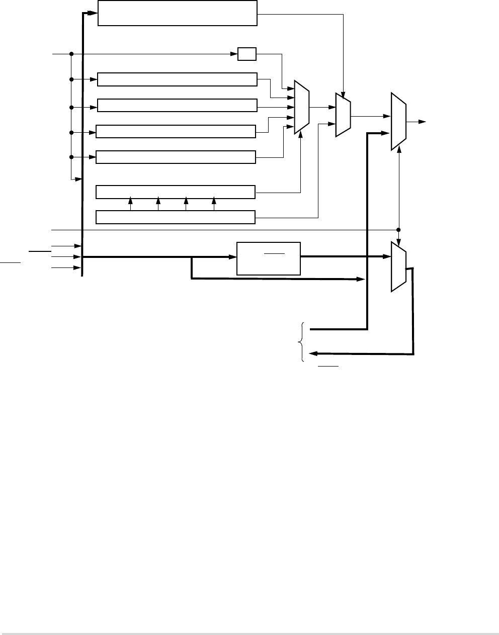
31-2 MCF5282 User’s Manual MOTOROLA
Features
Figure 31-1. JTAG Block Diagram
31.1 Features
The basic features of the JTAG module are the following:
• Performs boundary-scan operations to test circuit board electrical continuity
• Bypasses instruction to reduce the shift register path to a single cell
• Sets chip output pins to safety states while executing the bypass instruction
• Samples the system pins during operation and transparently shift out the result
• Selects between JTAG TAP controller and Background Debug Module (BDM)
using a dedicated JTAG_EN pin
4-BIT TAP INSTRUCTION REGISTER
30
1-BIT BYPASS REGISTER
148-BIT BOUNDARY SCAN REGISTER
32-BIT IDCODE REGISTER
TRST/DSCLK
TCLK
TMS/BKPT
031
0147
TAP CONTROLLER
TDI/DSI
1
0
TDO/DSO
JTAG Module
to Debug Module
7-BIT JTAG_CFM_CLKDIV REGISTER
0
6
3-BIT TEST_CTRL REGISTER
02
4-BIT TAP INSTRUCTION DECODER
1
0
Disable DSCLK
Force BKPT = 1
DSI = 0
JTAG_EN
DSO
DSI
BKPT
DSCLK
MOTOROLA Chapter 31. IEEE 1149.1 Test Access Port (JTAG) 31-3
Modes of Operation
31.2 Modes of Operation
The JTAG_EN pin can select between the following modes of operation:
• JTAG mode
• BDM - background debug mode (For more information, refer to Section 29.5,
“Background Debug Mode (BDM)).”
31.3 External Signal Description
The JTAG module has five input and one output external signals, as described in
Table 31-1.
31.3.1 Detailed Signal Description
31.3.1.1 JTAG_EN — JTAG Enable
The JTAG_EN pin selects between Debug module and JTAG. If JTAG_EN is low, the
Debug module is selected; if it is high, the JTAG is selected. Table 31-2 summarizes the pin
function selected depending upon JTAG_EN logic state.
When one module is selected, the inputs into the other module are disabled or forced to a
known logic level as shown in Table 31-3, in order to disable the corresponding module.
Table 31-1. Signal Properties
Name Direction Function Reset State Pull up
JTAG_EN Input JTAG/BDM selector input — —
TCLK Input JTAG Test clock input — Active
TMS/BKPT Input JTAG Test mode select / BDM Breakpoint — Active
TDI/DSI Input JTAG Test data input / BDM Development serial input — Active
TRST/DSCLK Input JTAG Test reset input / BDM Development serial clock — Active
TDO/DSO Output JTAG Test data output / BDM Development serial output Hi-Z / 0 —
Table 31-2. Pin Function Selected
JTAG_EN = 0 JTAG_EN = 1 Pin Name
Module selected BDM JTAG —
Pin Function —
BKPT
DSI
DSO
DSCLK
TCLK
TMS
TDI
TDO
TRST
TCLK
BKPT
DSI
DSO
DSCLK

31-4 MCF5282 User’s Manual MOTOROLA
External Signal Description
NOTE
The JTAG_EN does not support dynamic switching between
JTAG and BDM modes.
31.3.1.2 TCLK — Test Clock Input
The TCLK pin is a dedicated JTAG clock input to synchronize the test logic. Pulses on
TCLK shift data and instructions into the TDI pin on the rising edge and out of the TDO
pin on the falling edge. TCLK is independent of the processor clock. The TCLK pin has an
internal pull-up resistor and holding TCLK high or low for an indefinite period does not
cause JTAG test logic to lose state information.
31.3.1.3 TMS/BKPT — Test Mode Select / Breakpoint
The TMS pin is the test mode select input that sequences the TAP state machine. TMS is
sampled on the rising edge of TCLK. The TMS pin has an internal pull-up resistor.
The BKPT pin is used to request an external breakpoint. Assertion of BKPT puts the
processor into a halted state after the current instruction completes.
31.3.1.4 TDI/DSI — Test Data Input / Development Serial Input
The TDI pin is the LSB-first data and instruction input. TDI is sampled on the rising edge
of TCLK. The TDI pin has an internal pull-up resistor.
The DSI pin provides data input for the debug module serial communication port.
31.3.1.5 TRST/DSCLK — Test Reset / Development Serial Clock
The TRST pin is an active low asynchronous reset input with an internal pull-up resistor
that forces the TAP controller to the test-logic-reset state.
The DSCLK pin clocks the serial communication port to the debug module. Maximum
frequency is 1/5 the processor clock speed. At the rising edge of DSCLK, the data input on
DSI is sampled and DSO changes state.
Table 31-3. Signal State to the Disable Module
JTAG_EN = 0 JTAG_EN = 1
Disabling JTAG TRST = 0
TMS = 1
—
Disabling BDM — Disable DSCLK
DSI = 0
BKPT = 1

MOTOROLA Chapter 31. IEEE 1149.1 Test Access Port (JTAG) 31-5
Memory Map/Register Definition
31.3.1.6 TDO/DSO — Test Data Output / Development Serial Output
The TDO pin is the LSB-first data output. Data is clocked out of TDO on the falling edge
of TCLK. TDO is tri-stateable and is actively driven in the shift-IR and shift-DR controller
states.
The DSO pin provides serial output data in BDM mode.
31.4 Memory Map/Register Definition
31.4.1 Memory Map
The JTAG module registers are not memory mapped and are only accessible through the
TDO/DSO pin.
31.4.2 Register Descriptions
All registers are shift-in and parallel load.
31.4.2.1 Instruction Shift Register (IR)
The JTAG module uses a 4-bit shift register with no parity. The IR transfers its value to a
parallel hold register and applies an instruction on the falling edge of TCLK when the TAP
state machine is in the update-IR state. To load an instruction into the shift portion of the
IR, place the serial data on the TDI pin before each rising edge of TCLK. The MSB of the
IR is the bit closest to the TDI pin, and the LSB is the bit closest to the TDO pin.
31.4.2.2 IDCODE Register
The IDCODE is a read-only register; its value is chip dependent. For more information, see
Section 31.5.3.2, “IDCODE Instruction.”
31 28 27 22 21 16
Field PRN[[3:0] DC[5:0] PIN[9:0]
Reset PRN[3] PRN[2] PRN[1] PRN[0] 0111_01 PIN[9] PIN[8] PIN[7] PIN[6] PIN[5] PIN[4]
R/W Read only
15 12 11 10
Field PIN[9:0] JEDEC[10] ID
Reset 0000_0000_0000_0000
R/W Read only
Figure 31-2. IDCODE Register

31-6 MCF5282 User’s Manual MOTOROLA
Memory Map/Register Definition
31.4.2.3 Bypass Register
The bypass register is a single-bit shift register path from TDI to TDO when the BYPASS
instruction is selected.
31.4.2.4 JTAG_CFM_CLKDIV Register
The JTAG_CFM_CLKDIV register is a 7-bit clock divider for the CFM that is used with
the LOCKOUT_RECOVERY instruction. It controls the period of the clock used for timed
events in the CFM erase algorithm. The JTAG_CFM_CLKDIV register must be loaded
before the lockout sequence can begin.
31.4.2.5 TEST_CTRL Register
The TEST_CTRL register is a 3-bit shift register path from TDI to TDO when the
ENABLE_TEST_CTRL instruction is selected. The TEST_CTRL transfers its value to a
parallel hold register on the rising edge of TCLK when the TAP state machine is in the
update-DR state.
31.4.2.6 Boundary Scan Register
The boundary scan register is connected between TDI and TDO when the EXTEST or
SAMPLE/PRELOAD instruction is selected. It captures input pin data, forces fixed values
on output pins, and selects a logic value and direction for bidirectional pins or high
impedance for tri-stated pins.
The boundary scan register contains bits for bonded-out and non bonded-out signals
excluding JTAG signals, analog signals, power supplies, compliance enable pins, and clock
signals.
Table 31-4. IDCODE Register Field Descriptions
Bits Name Description
31–28 PRN Part revision number. Indicate the revision number of the project.
27–22 DC Design center.
21–12 PIN Part identification number. Indicate the device number.
11–1 JEDEC Joint electron device engineering council ID bits. Indicate the reduced JEDEC ID for Motorola.
0 ID IDCODE register ID. This bit is set to 1 to identify the register as the IDCODE register and not the
bypass register according to the IEEE standard 1149.1.

MOTOROLA Chapter 31. IEEE 1149.1 Test Access Port (JTAG) 31-7
Functional Description
31.5 Functional Description
31.5.1 JTAG Module
The JTAG module consists of a TAP controller state machine, which is responsible for
generating all control signals that execute the JTAG instructions and read/write data
registers.
31.5.2 TAP Controller
The TAP controller is a state machine that changes state based on the sequence of logical
values on the TMS pin. Figure 31-3 shows the machine’s states. The value shown next to
each state is the value of the TMS signal sampled on the rising edge of the TCLK signal.
Asserting the TRST signal asynchronously resets the TAP controller to the test-logic-reset
state. As Figure 31-3 shows, holding TMS at logic 1 while clocking TCLK through at least
five rising edges also causes the state machine to enter the test-logic-reset state, whatever
the initial state.
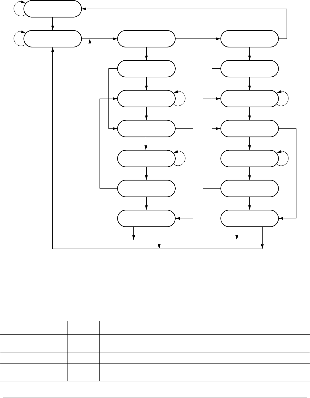
31-8 MCF5282 User’s Manual MOTOROLA
Functional Description
Figure 31-3. TAP Controller State Machine Flow
31.5.3 JTAG Instructions
Table 31-5 describes public and private instructions.
Table 31-5. JTAG Instructions
Instruction IR[3:0] Instruction Summary
EXTEST 0000 Selects boundary scan register while applying fixed values to output pins and asserting
functional reset
IDCODE 0001 Selects IDCODE register for shift
SAMPLE/PRELOAD 0010 Selects boundary scan register for shifting, sampling, and preloading without
disturbing functional operation
RUN-TEST/IDLE
TEST-LOGIC-RESET
1
1
SELECT DR-SCAN
CAPTURE-DR
EXIT1-DR
PAUSE-DR
UPDATE-DR
SELECT IR-SCAN
SHIFT-DR
EXIT2-DR
CAPTURE-IR
SHIFT-IR
EXIT1-IR
PAUSE-IR
EXIT2-IR
UPDATE-IR
0
0
1
1
0
0
0
1
1
10
0
0
1
1
0
0
1
1
0
1
0
1
10
1
1
0
0
1
0

MOTOROLA Chapter 31. IEEE 1149.1 Test Access Port (JTAG) 31-9
Functional Description
31.5.3.1 External Test Instruction (EXTEST)
The EXTEST instruction selects the boundary scan register. It forces all output pins and
bidirectional pins configured as outputs to the values preloaded with the
SAMPLE/PRELOAD instruction and held in the boundary scan update registers. EXTEST
can also configure the direction of bidirectional pins and establish high-impedance states
on some pins. EXTEST asserts internal reset for the MCU system logic to force a
predictable internal state while performing external boundary scan operations.
31.5.3.2 IDCODE Instruction
The IDCODE instruction selects the 32-bit IDCODE register for connection as a shift path
between the TDI and TDO pin. This instruction allows interrogation of the MCU to
determine its version number and other part identification data. The shift register LSB is
forced to logic 1 on the rising edge of TCLK following entry into the capture-DR
state.Therefore, the first bit to be shifted out after selecting the IDCODE register is always
a logic 1. The remaining 31 bits are also forced to fixed values on the rising edge of TCLK
following entry into the capture-DR state.
IDCODE is the default instruction placed into the instruction register when the TAP resets.
Thus, after a TAP reset, the IDCODE register is selected automatically.
31.5.3.3 SAMPLE/PRELOAD Instruction
The SAMPLE/PRELOAD instruction has two functions:
• SAMPLE - obtain a sample of the system data and control signals present at the
MCU input pins and just before the boundary scan cell at the output pins. This
sampling occurs on the rising edge of TCLK in the capture-DR state when the IR
TEST_LEAKAGE 1, 2 0101 Selects bypass register while tri-stating all output pins and assert to high the
jtag_leakage signal
ENABLE_TEST_CTRL 0110 Selects TEST_CTRL register
HIGHZ 1001 Selects bypass register while tri-stating all output pins and asserting functional reset
LOCKOUT_RECOVERY 1011 Allows for the erase of the TFM flash when the part is secure
CLAMP 1100 Selects bypass while applying fixed values to output pins and asserting functional
reset
BYPASS 1111 Selects bypass register for data operations
Reserved all others Decoded to select bypass register 3
1Instruction for manufacturing purposes only
2TRST pin assertion or power-on reset is required to exit this instruction.
3Motorola reserves the right to change the decoding of the unused opcodes in the future.
Table 31-5. JTAG Instructions (continued)
Instruction IR[3:0] Instruction Summary

31-10 MCF5282 User’s Manual MOTOROLA
Functional Description
contains the $2 opcode. The sampled data is accessible by shifting it through the
boundary scan register to the TDO output by using the shift-DR state. Both the data
capture and the shift operation are transparent to system operation.
NOTE
External synchronization is required to achieve meaningful
results because there is no internal synchronization between
TCLK and the system clock.
• PRELOAD - initialize the boundary scan register update cells before selecting
EXTEST or CLAMP. This is achieved by ignoring the data shifting out on the TDO
pin and shifting in initialization data. The update-DR state and the falling edge of
TCLK can then transfer this data to the update cells. The data is applied to the
external output pins by the EXTEST or CLAMP instruction.
31.5.3.4 TEST_LEAKAGE Instruction
The TEST_LEAKAGE instruction forces the jtag_leakage output signal to high. It is
intended to tri-state all output pad buffers and disable all of the part’s pad input buffers
except TEST and TRST. The jtag_leakage signal is asserted at the rising edge of TCLK
when the TAP controller transitions from update-IR to run-test/idle state. Once asserted, the
part disables the TCLK, TMS, and TDI inputs into JTAG and forces these JTAG inputs to
logic 1. The TAP controller remains in the run-test/idle state until the TRST input is
asserted (logic 0).
31.5.3.5 ENABLE_TEST_CTRL Instruction
The ENABLE_TEST_CTRL instruction selects a 3-bit shift register (TEST_CTRL) for
connection as a shift path between the TDI and TDO pin. When the user transitions the TAP
controller to the UPDATE_DR state, the register transfers its value to a parallel hold
register. It allows the control chip to test functions independent of the JTAG TAP controller
state.
31.5.3.6 HIGHZ Instruction
The HIGHZ instruction eliminates the need to backdrive the output pins during
circuit-board testing. HIGHZ turns off all output drivers, including the 2-state drivers, and
selects the bypass register. HIGHZ also asserts internal reset for the MCU system logic to
force a predictable internal state.
31.5.3.7 LOCKOUT_RECOVERY Instruction
If a user inadvertently enables security on a MCU, the LOCKOUT_RECOVERY
instruction allows the disabling of security by the complete erasure of the internal flash
contents including the configuration field. This does not compromise security as the entire

MOTOROLA Chapter 31. IEEE 1149.1 Test Access Port (JTAG) 31-11
Initialization/Application Information
contents of the user’s secured code stored in flash gets erased before security is disabled on
the MCU on the next reset or power-up sequence.
The LOCKOUT_RECOVERY instruction selects a 7-bit shift register for connection as a
shift path between the TDI pin and the TDO pin. When the user transitions the TAP
controller to the UPDATE-DR state, the 7-bit shift register is loaded into the 7-bit
JTAG_TFM_CLKDIV register and this value is output to the TFM’s clock divider circuit.
When the user transitions the TAP controller to the RUN-TEST/IDLE state, the erase signal
to the TFM asserts and the lockout sequence starts. The controller must remain in that state
until the erase sequence has completed. Once the lockout recovery sequence has completed,
the user must reset both the JTAG TAP controller and the MCU to return to normal
operation.
31.5.3.8 CLAMP Instruction
The CLAMP instruction selects the bypass register and asserts internal reset while
simultaneously forcing all output pins and bidirectional pins configured as outputs to the
fixed values that are preloaded and held in the boundary scan update register. CLAMP
enhances test efficiency by reducing the overall shift path to a single bit (the bypass
register) while conducting an EXTEST type of instruction through the boundary scan
register.
31.5.3.9 BYPASS Instruction
The BYPASS instruction selects the bypass register, creating a single-bit shift register path
from the TDI pin to the TDO pin. BYPASS enhances test efficiency by reducing the overall
shift path when a device other than the ColdFire processor is the device under test on a
board design with multiple chips on the overall boundary scan chain. The shift register LSB
is forced to logic 0 on the rising edge of TCLK after entry into the capture-DR state.
Therefore, the first bit shifted out after selecting the bypass register is always logic 0. This
differentiates parts that support an IDCODE register from parts that support only the bypass
register.
31.6 Initialization/Application Information
31.6.1 Restrictions
The test logic is a static logic design, and TCLK can be stopped in either a high or low state
without loss of data. However, the system clock is not synchronized to TCLK internally.
Any mixed operation using both the test logic and the system functional logic requires
external synchronization.

31-12 MCF5282 User’s Manual MOTOROLA
Initialization/Application Information
Using the EXTEST instruction requires a circuit-board test environment that avoids
device-destructive configurations in which MCU output drivers are enabled into actively
driven networks.
Low-power stop mode considerations:
• The TAP controller must be in the test-logic-reset state to either enter or remain in
the low-power stop mode. Leaving the test-logic-reset state negates the ability to
achieve low-power, but does not otherwise affect device functionality.
• The TCLK input is not blocked in low-power stop mode. To consume minimal
power, the TCLK input should be externally connected to VDD.
• The TMS, TDI, and TRST pins include on-chip pull-up resistors. For minimal
power consumption in low-power stop mode, these three pins should be either
connected to VDD or left unconnected.
31.6.2 Nonscan Chain Operation
Keeping the TAP controller in the test-logic-reset state ensures that the scan chain test logic
is transparent to the system logic. It is recommended that TMS, TDI, TCLK, and TRST be
pulled up. TRST could be connected to ground. However, since there is a pull-up on TRST,
some amount of current results. The internal power-on reset input initializes the TAP
controller to the test-logic-reset state on power-up without asserting TRST.

MOTOROLA Chapter 32. Mechanical Data 32-1
Chapter 32
Mechanical Data
This chapter contains drawings showing the pinout and the packaging and mechanical
characteristics of the MCF5282.

32-2 MCF5282 User’s Manual MOTOROLA
Pinout
32.1 Pinout
Figure 32-1 is a pinout for the MCF5282.
Figure 32-1. MCF5282 Pinout (256 MAPBGA)
Table 32-1 lists the MCF5282 signals in pin number order for the 256 MAPBGA package
123456 7 8 910111213 14 15 16
AVSS A15 A16 A18 A21 VPP ETXD3 ETXCLK ERXD3 ERXCLK ECRS VDDF DDATA1 PST2 PST0 VSS
BA14 A13 A17 A19 VSSF A22 ETXD2 ERXER ERXD2 EMDC ECOL VSSF DDATA0 PST1 IRQ7 IRQ6
CA12 A11 A10 A20 VDDF A23 ETXD1 ERXDV ERXD1 EMDIO VPP DDATA3 PST3 IRQ5 IRQ4 IRQ3
DA9 A8 A7 A6 VDDF ETXEN ETXD0 NC ERXD0 ETXER VDDF DDATA2 NC IRQ2 IRQ1 CANRX
EA5 A4 A3 A2 VSS VDD VDD VDD VDD VDD VDD VSS CANTX SDA SCL QSPI_
DIN
FA1 A0 D31 NC VDD VSS VDD VDD VDD VDD VSS VDD QSPI_
DOUT
QSPI_
CLK
QSPI_
CS0
QSPI_
CS1
GD30 D29 D28 D27 VDD VDD VSS VSS VSS VSS VDD VDD QSPI_
CS2
QSPI_
CS3 DRAMW SDRAM_
CS0
HD26 D25 D24 D23 VDD VDD VSS VSS VSS VSS VDD VDD SDRA_
CS1 SCKE SRAS SCAS
JD22 D21 D20 D19 VDD VDD VSS VSS VSS VSS VDD VDD DTOUT0 DTIN0 DTOUT1 DTIN1
KD18 D17 D16 NC VDD VDD VSS VSS VSS VSS VDD VDD DTOUT2 DTIN2 DTOUT3 DTIN3
LD15 D14 D13 D12 VDD VSS VDD VDD VDD VDD VSS VDD CS0 CS1 CS2 CS3
MD11 D10 D9 D8 VSS VDD VDD VDD VDD VDD VDD VSS NC TIP TS SIZ0
ND7 D6 D5 NC D3 URXD0 CLKOUT VDDPLL NC TEST VSTBY GPTB0 GPTA0 SIZ1 R/W OE
PD4 VDDH AN55 VRH VSSA D0 UTXD1 VSSPLL DSCLK BKPT RSTO GPTB1 GPTA1 BS3 TEA TA
RAN3 AN1 AN56 AN52 VDDA D1 URXD1 XTAL JTAG_E
NDSI RSTI GPTB2 GPTA2 CLKMOD0 BS1 BS0
TVSSA AN2 AN0 AN53 VRL D2 UTXD0 EXTAL TCLK DSO RCON GPTB3 GPTA3 CLKMOD1 BS2 VSS

MOTOROLA Chapter 32. Mechanical Data 32-3
Pinout
Table 32-1. MCF5282 Signal Description by Pin Number
MAPBGA Pin
Pin Functions
MAPBGA Pin
Pin Functions
Primary Secondary Tertiary Primary Secondary Tertiary
A1 VSS J1 D22 PB6
A2 A15 PG7 J2 D21 PB5
A3 A16 PF0 J3 D20 PB4
A4 A18 PF2 J4 D19 PB3
A5 A21 PF5 CS4 J5 VDD
A6 VPP J6 VDD
A7 ETXD3 PEL7 J7 VSS
A8 ETXCLK PEH7 J8 VSS
A9 ERXD3 PEL3 J9 VSS
A10 ERXCLK PEH3 J10 VSS
A11 ECRS PEH0 J11 VDD
A12 VDDF J12 VDD
A13
DDATA1 PDD5 J13 DTOUT0 PTD0 UCTS1/
UCTS0
A14 PST2 PDD2 J14 DTIN0 PTD1 UCTS1/UCTS0
A15 PST0 PDD0 J15 DTOUT1 PTD2 URTS1/URTS0
A16 VSS J16 DTIN1 PTD3 URTS1/URTS0
B1 A14 PG6 K1 D18 PB2
B2 A13 PG5 K2 D17 PB1
B3 A17 PF1 K3 D16 PB0
B4 A19 PF3 K4 NC1
B5 VSSF K5 VDD
B6 A22 PF6 CS5 K6 VDD
B7 ETXD2 PEL6 K7 VSS
B8 ERXER PEL0 K8 VSS
B9 ERXD2 PEL2 K9 VSS
B10 EMDC PAS4 UTXD2 K10 VSS
B11 ECOL PEH4 K11 VDD
B12 VSSF K12 VDD
B13 DDATA0 PDD4 K13 DTOUT2 PTC0 UCTS1/UCTS0
B14 PST1 PDD1 K14 DTIN2 PTC1 UCTS1/UCTS0
B15 IRQ7 PNQ7 K15 DTOUT3 PTC2 URTS1/URTS0
B16 IRQ6 PNQ6 K16 DTIN3 PTC3 URTS1/URTS0

32-4 MCF5282 User’s Manual MOTOROLA
Pinout
C1 A12 PG4 L1 D15 PC7
C2 A11 PG3 L2 D14 PC6
C3 A10 PG2 L3 D13 PC5
C4 A20 PF4 L4 D12 PC4
C5 VDDF L5 VDD
C6 A23 PF7 CS6 L6 VSS
C7 ETXD1 PEL5 L7 VDD
C8 ERXDV PEH2 L8 VDD
C9 ERXD1 PEL1 L9 VDD
C10 EMDIO PAS5 URXD2 L10 VDD
C11 VPP L11 VSS
C12 DDATA3 PDD7 L12 VDD
C13 PST3 PDD3 L13 CS0 PJ0
C14 IRQ5 PNQ5 L14 CS1 PJ1
C15 IRQ4 PNQ4 L15 CS2 PJ2
C16 IRQ3 PNQ3 L16 CS3 PJ3
D1 A9 PG1 M1 D11 PC3
D2 A8 PG0 M2 D10 PC2
D3 A7 PH7 M3 D9 PC1
D4 A6 PH6 M4 D8 PC0
D5 VDDF M5 VSS
D6 ETXEN PEH6 M6 VDD
D7 ETXD0 PEH5 M7 VDD
D8 NC M8 VDD
D9 ERXD0 PEH1 M9 VDD
D10 ETXER PEL4 M10 VDD
D11 VDDF M11 VDD
D12 DDATA2 PDD6 M12 VSS
D13 NC M13 NC
D14 IRQ2 PNQ2 M14 TIP PE0 SYNCB
D15 IRQ1 PNQ1 M15 TS PE1 SYNCA
D16 CANRX PAS3 URXD2 M16 SIZ0 PE2 SYNCB
E1 A5 PH5 N1 D7 PD7
Table 32-1. MCF5282 Signal Description by Pin Number (Continued)
MAPBGA Pin
Pin Functions
MAPBGA Pin
Pin Functions
Primary Secondary Tertiary Primary Secondary Tertiary

MOTOROLA Chapter 32. Mechanical Data 32-5
Pinout
E2 A4 PH4 N2 D6 PD6
E3 A3 PH3 N3 D5 PD5
E4 A2 PH2 N4 NC
E5 VSS N5 D3 PD3
E6 VDD N6 URXD0 PUA1
E7 VDD N7 CLKOUT
E8 VDD N8 VDDPLL
E9 VDD N9 NC
E10 VDD N10 TEST
E11 VDD N11 VSTBY
E12 VSS N12 GPTB0 PTB0
E13 CANTX PAS2 UTXD2 N13 GPTA0 PTA0
E14 SDA PAS1 URXD2 N14 SIZ1 PE3 SYNCA
E15 SCL PAS0 UTXD2 N15 R/W PE4
E16 QSPI_DIN PQS1 N16 OE PE7
F1 A1 PH1 P1 D4 PD4
F2 A0 PH0 P2 VDDH
F3 D31 PA7 P3 AN55 PQA3 ETRIG1
F4 NC P4 VRH
F5 VDD P5 VSSA
F6 VSS P6 D0 PD0
F7 VDD P7 UTXD1 PUA2
F8 VDD P8 VSSPLL
F9 VDD P9 DSCLK TRST
F10 VDD P10 BKPT TMS
F11 VSS P11 RSTO
F12 VDD P12 GPTB1 PTB1
F13 QSPI_DOUT PQS0 P13 GPTA1 PTA1
F14 QSPI_CLK PQS2 P14 BS3 PJ7
F15 QSPI_CS0 PQS3 P15 TEA PE5
F16 QSPI_CS1 PQS4 P16 TA PE6
G1 D30 PA6 R1 AN3 PQB3 ANZ
G2 D29 PA5 R2 AN1 PQB1 ANX
Table 32-1. MCF5282 Signal Description by Pin Number (Continued)
MAPBGA Pin
Pin Functions
MAPBGA Pin
Pin Functions
Primary Secondary Tertiary Primary Secondary Tertiary

32-6 MCF5282 User’s Manual MOTOROLA
Pinout
G3 D28 PA4 R3 AN56 PQA4 ETRIG2
G4 D27 PA3 R4 AN52 PQA0 MA0
G5 VDD R5 VDDA
G6 VDD R6 D1 PD1
G7 VSS R7 URXD1 PUA3
G8 VSS R8 XTAL
G9 VSS R9 JTAG_EN
G10 VSS R10 DSI TDI
G11 VDD R11 RSTI
G12 VDD R12 GPTB2 PTB2
G13 QSPI_CS2 PQS5 R13 GPTA2 PTA2
G14 QSPI_CS3 PQS6 R14 CLKMOD0
G15 DRAMW PSD3 R15 BS1 PJ5
G16 SDRAM_CS0 PSD1 R16 BS0 PJ4
H1 D26 PA2 T1 VSSA
H2 D25 PA1 T2 AN2 PQB2 ANY
H3 D24 PA0 T3 AN0 PQB0 ANW
H4 D23 PB7 T4 AN53 PQA1 MA1
H5 VDD T5 VRL
H6 VDD T6 D2 PD2
H7 VSS T7 UTXD0 PUA0
H8 VSS T8 EXTAL
H9 VSS T9 TCLK
H10 VSS T10 DSO TDO
H11 VDD T11 RCON
H12 VDD T12 GPTB3 PTB3
H13 SDRAM_CS1 PSD2 T13 GPTA3 PTA3
H14 SCKE PSD0 T14 CLKMOD1
H15 SRAS PSD5 T15 BS2 PJ6
H16 SCAS PSD4 T16 VSS
1No connect
Table 32-1. MCF5282 Signal Description by Pin Number (Continued)
MAPBGA Pin
Pin Functions
MAPBGA Pin
Pin Functions
Primary Secondary Tertiary Primary Secondary Tertiary
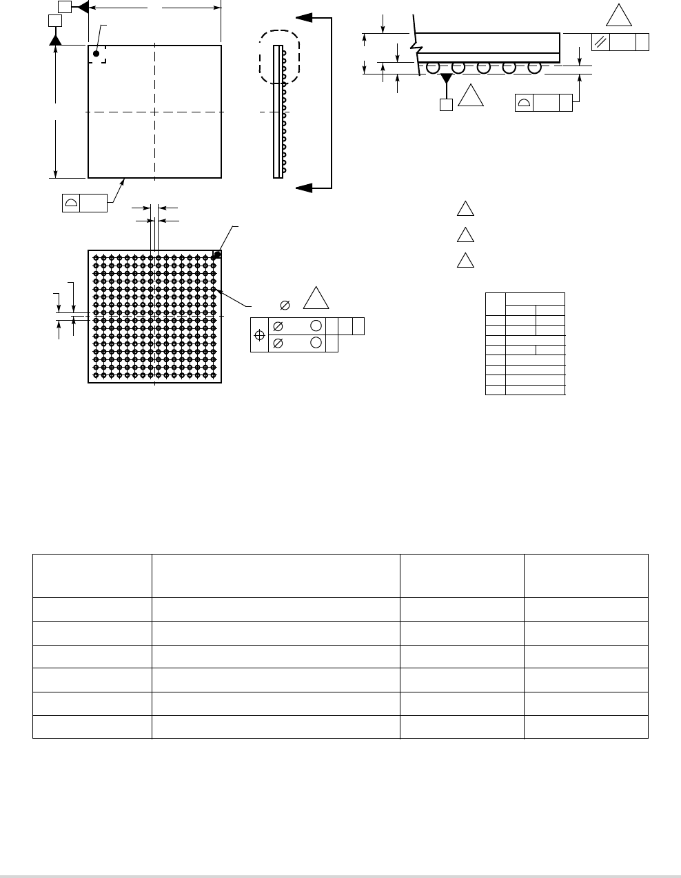
MOTOROLA Chapter 32. Mechanical Data 32-7
Ordering Information
Figure 32-2. 256 MAPBGA Package Dimensions
32.2 Ordering Information
Table 32-2. Orderable Part Numbers
Motorola Part
Number Description Speed Temperature
MCF5280CVF66 MCF5280 RISC Microprocessor, 256 MAPBGA 66.67 MHz -40° to +85° C
MCF5280CVF80 MCF5280 RISC Microprocessor, 256 MAPBGA 80 MHz -40° to +85° C
MCF5281CVF66 MCF5281 RISC Microprocessor, 256 MAPBGA 66.67 MHz -40° to +85° C
MCF5281CVF80 MCF5281 RISC Microprocessor, 256 MAPBGA 80 MHz -40° to +85° C
MCF5282CVF66 MCF5282 RISC Microprocessor, 256 MAPBGA 66.67 MHz -40° to +85° C
MCF5282CVF80 MCF5282 RISC Microprocessor, 256 MAPBGA 80 MHz -40° to +85° C
X
Y
D
E
LASER MARK FOR PIN A1
IDENTIFICATION IN
THIS AREA
0.20
METALIZED MARK FOR
PIN A1 IDENTIFICATION
IN THIS AREA
M
M
3
A
B
C
D
E
F
G
H
J
K
L
M
N
P
R
T
123456710111213141516
e15X
e15X
b256X
M
0.25 YZ
M
0.10
X
Z
S
DETAIL K
VIEW M-M
ROTATED 90 CLOCKWISE
°
S
A
ZZ
A2
A1
40.15
Z0.30
256X
5
K
NOTES:
1. DIMENSIONS ARE IN MILLIMETERS.
2. INTERPRET DIMENSIONS AND TOLERANCES
PER ASME Y14.5M, 1994.
3. DIMENSION b IS MEASURED AT THE
MAXIMUM SOLDER BALL DIAMETER,
PARALLEL TO DATUM PLANE Z.
4. DATUM Z (SEATING PLANE) IS DEFINED BY
THE SPHERICAL CROWNS OF THE SOLDER
BALLS.
5. PARALLELISM MEASUREMENT SHALL
DIM MIN MAX
MILLIMETERS
A1.25 1.60
A1 0.27 0.47
A2 1.16 REF
b0.40 0.60
D17.00 BSC
E17.00 BSC
e1.00 BSC
S0.50 BSC

32-8 MCF5282 User’s Manual MOTOROLA
Ordering Information

MOTOROLA Chapter 33. Electrical Characteristics 33-1
Chapter 33
Electrical Characteristics
This chapter contains electrical specification tables and reference timing diagrams for the
MCF5282 microcontroller unit. This section contains detailed information on power
considerations, DC/AC electrical characteristics, and AC timing specifications of
MCF5282.
The electrical specifications are preliminary and are from previous designs or design
simulations. These specifications may not be fully tested or guaranteed at this early stage
of the product life cycle; however, these specifications will be met for production silicon.
Finalized specifications will be published after complete characterization and device
qualifications have been completed.
NOTE:
The parameters specified in this MCU document supersede any
values found in the module specifications.
33.1 Maximum Ratings
Table 33-1. Absolute Maximum Ratings1, 2
Rating Symbol Value Unit
Supply Voltage VDD – 0.3 to +4.0 V
Clock Synthesizer Supply Voltage VDDPLL – 0.3 to +4.0 V
RAM Memory Standby Supply Voltage VSTBY – 0.3 to + 4.0 V
Flash Memory Supply Voltage VDDF – 0.3 to +4.0 V
Flash Memory Program / Erase Supply Voltage VPP – 0.3 to + 6.0 V
Analog Supply Voltage VDDA – 0.3 to +6.0 V
Analog Reference Supply Voltage VRH – 0.3 to +6.0 V
Analog ESD Protection Voltage VDDH – 0.3 to +6.0 V
Digital Input Voltage 3VIN – 0.3 to + 6.0 V
Analog Input Voltage VAIN – 0.3 to + 6.0 V
EXTAL pin voltage VEXTAL 0 to 3.3 V
XTAL pin voltage VXTAL 0 to 3.3 V

33-2 MCF5282 User’s Manual MOTOROLA
Maximum Ratings
Instantaneous Maximum Current
Single pin limit (applies to all pins) 3, 4, 5
ID25 mA
Operating Temperature Range (Packaged) TA– 40 to 85 °C
Storage Temperature Range Tstg – 65 to 150 °C
Maximum operating junction temperature Tj105 oC
ESD Target for Human Body Model6HBM 2000 V
1Functional operating conditions are given in DC Electrical Specifications. Absolute Maximum
Ratings are stress ratings only, and functional operation at the maxima is not guaranteed.
Stress beyond those listed may affect device reliability or cause permanent damage to the
device.
2This device contains circuitry protecting against damage due to high static voltage or
electrical fields; however, it is advised that normal precautions be taken to avoid application of
any voltages higher than maximum-rated voltages to this high-impedance circuit. Reliability of
operation is enhanced if unused inputs are tied to an appropriate logic voltage level (e.g.,
either VSS or VDD).
3Input must be current limited to the value specified. To determine the value of the required
current-limiting resistor, calculate resistance values for positive and negative clamp voltages,
then use the larger of the two values. 6.0V voltage excludes XTAL and EXTAL pads.
4All functional non-supply pins are internally clamped to VSS and VDD.
5Power supply must maintain regulation within operating VDD range during instantaneous and
operating maximum current conditions. If positive injection current (Vin > VDD) is greater than
IDD, the injection current may flow out of VDD and could result in external power supply going
out of regulation. Insure external VDD load will shunt current greater than maximum injection
current. This will be the greatest risk when the MCU is not consuming power (ex; no
clock).Power supply must maintain regulation within operating VDD range during
instantaneous and operating maximum current conditions.
6All ESD testing methodology is in conformity with CDF-AEC-Q100 Stress Test
Qualification for Automotive Grade Integrated Circuits.
Table 33-1. Absolute Maximum Ratings1, 2 (Continued)
Rating Symbol Value Unit

MOTOROLA Chapter 33. Electrical Characteristics 33-3
Thermal Characteristics
33.2 Thermal Characteristics
Table 33-2 lists thermal resistance values.
Table 33-2. Thermal Characteristics
Characteristic Symbol Value Unit
Junction to ambient, natural convection Four layer board (2s2p) θJMA 261,2
1θJMA and Ψjt parameters are simulated in accordance with EIA/JESD Standard 51-2 for natural convection.
Motorola recommends the use of θJA and power dissipation specifications in the system design to prevent device
junction temperatures from exceeding the rated specification. System designers should be aware that device
junction temperatures can be significantly influenced by board layout and surrounding devices. Conformance to
the device junction temperature specification can be verified by physical measurement in the customer’s system
using the Ψjt parameter, the device power dissipation, and the method described in EIA/JESD Standard 51-2.
2Per JEDEC JESD51-6 with the board horizontal.
°C/W
Junction to ambient (@200 ft/min) Four layer board (2s2p) θJMA 231,2 °C/W
Junction to board θJB 153
3Thermal resistance between the die and the printed circuit board per JEDEC JESD51-8. Board temperature is
measured on the top surface of the board near the package.
°C/W
Junction to case θJC 104
4Thermal resistance between the die and the case top surface as measured by the cold plate method (MIL
SPEC-883 Method 1012.1).
°C/W
Junction to top of package Natural convection Ψjt 21,5
5Thermal characterization parameter indicating the temperature difference between package top and the junction
temperature per JEDEC JESD51-2. When Greek letters are not available, the thermal characterization parameter
is written as Psi-JT.
°C/W
The average chip-junction temperature (TJ) in °C can be obtained from:
(1)
Where:
TA= Ambient Temperature, ×C
QJMA= Package Thermal Resistance, Junction-to-Ambient, ×C/W
PD= PINT + PI/O
PINT= IDD ¥ VDD, Watts - Chip Internal Power
PI/O= Power Dissipation on Input and Output Pins — User Determined
For most applications PI/O < PINT and can be neglected. An approximate relationship
between PD and TJ (if PI/O is neglected) is:
T
JTAPDΘJMA
×(
)
+=

33-4 MCF5282 User’s Manual MOTOROLA
DC Electrical Specifications
33.3 DC Electrical Specifications
(2)
Solving equations 1 and 2 for K gives:
K = PD × (TA + 273 × C) + QJMA × PD 2 (3)
where K is a constant pertaining to the particular part. K can be determined from equation
(3) by measuring PD (at equilibrium) for a known TA. Using this value of K, the values
of PD and TJ can be obtained by solving equations (1) and (2) iteratively for any value of
TA.
Table 33-3. DC Electrical Specifications1
(VSS = VSSPLL= VSSF = VSSA= 0 VDC)
Characteristic Symbol Min Max Unit
Input High Voltage VIH 0.7 x VDD 5.25 V
Input Low Voltage VIL VSS – 0.3 0.35 x VDD V
Input Hysteresis VHYS 0.06 x
VDD
—mV
Input Leakage Current
Vin = VDD or VSS, Input-only pins
Iin -1.0 1.0 µA
High Impedance (Off-State) Leakage Current
Vin = VDD or VSS, All input/output and output pins
IOZ -1.0 1.0 µA
Output High Voltage (All input/output and all output pins)
IOH = –2.0 mA
VOH VDD - 0.5 __ V
Output Low Voltage (All input/output and all output pins)
IOL = 2.0mA
VOL __ 0.5 V
Weak Internal Pull Up Device Current, tested at VIL Max. IAPU -10 -130 µA
Input Capacitance 2
All input-only pins
All input/output (three-state) pins
Cin
—
—
7
7
pF
Load Capacitance3
(50% Partial Drive)
(100% Full Drive)
CL25
50
pF
Supply Voltage (includes core modules and pads) VDD 2.7 3.6 V
RAM Memory Standby Supply Voltage
Normal Operation: VDD > VSTBY - 0.3 V
Standby Mode: VDD < VSTBY - 0.3 V
VSTBY
0.0
1.8
3.6
3.6
V
Flash Memory Supply Voltage
VDDF 2.7 3.6
V
PDKT
J273°C+()÷=

MOTOROLA Chapter 33. Electrical Characteristics 33-5
DC Electrical Specifications
Operating Supply Current 4
Master Mode
• 66 MHz
• 80 MHz
Single Chip Mode
WAIT
DOZE
STOP
IDD
—
—
—
—
—
—
200
240
150
15
10
1000
mA
mA
mA
mA
µA
Clock Synthesizer Supply Current
Normal Operation 8.25 MHz crystal, VCO on, Max fsys
STOP (OSC and PLL enabled)
STOP (OSC enable, PLL disabled)
STOP (OSC and PLL disabled)
IDDPLL
—
—
—
—
4
2
1
10
mA
mA
mA
µA
RAM Memory Standby Supply Current
Normal Operation: VDD > VSTBY - 0.3 V
Transient Condition: VSTBY - 0.3 V > VDD > VSS + 0.5 V
Standby Operation: VDD < VSS + 0.5 V
ISTBY
—
—
—
10
7
20
µA
mA
µA
Flash Memory Supply Current
Read
Program or Erase5
Idle
STOP
IDDF
—
—
—
—
30
64
20
10
mA
mA
mA
µA
Analog Supply Current
Normal Operation
Low-Power Stop
IDDA
—
—
5.0
10.0
mA
µµAµ
1Refer to Table 33-4 through Table 33-8 for additional PLLQADC, and Flash specifications.
2This parameter is characterized before qualification rather than 100% tested.
3Refer to the chip configuration section for more information. Drivers for the SDRAM pins are at 25pF
drive strength.Drivers for the QADC pins are at 50pF drive strength.
4Current measured at maximum system clock frequency, all modules active, and default drive
strength with matching load.
5Programming and erasing all 8 blocks of the Flash.
Table 33-3. DC Electrical Specifications1 (Continued)
(VSS = VSSPLL= VSSF = VSSA= 0 VDC)
Characteristic Symbol Min Max Unit

33-6 MCF5282 User’s Manual MOTOROLA
Phase Lock Loop Electrical Specifications
33.4 Phase Lock Loop Electrical Specifications
Table 33-4. PLL Electrical Specifications
(VDD and VDDPLL = 2.7 to 3.6 V, VSS = VSSPLL = 0 V)
Characteristic Symbol Min Max Unit
PLL Reference Frequency Range
Crystal reference
External reference
1:1 Mode
fref_crystal
fref_ext
fref_1:1
2
2
33.33
10.0
10.0
80
MHz
System Frequency 1
External Clock Mode
On-Chip PLL Frequency
1All internal registers retain data at 0 Hz.
fsys
0
fref / 32
80
80
MHz
Loss of Reference Frequency 2, 4
2“Loss of Reference Frequency” is the reference frequency detected internally, which transitions the PLL into
self clocked mode.
fLOR 100 1000 kHz
Self Clocked Mode Frequency 3, 4
3Self clocked mode frequency is the frequency that the PLL operates at when the reference frequency falls
below fLOR with default MFD/RFD settings.
fSCM 15MHz
Crystal Start-up Time 4, 5
4This parameter is characterized before qualification rather than 100% tested.
5Proper PC board layout procedures must be followed to achieve specifications.
tcst —10ms
EXTAL Input High Voltage
Crystal Mode
All other modes (1:1, Bypass, External)
VIHEXT
VDD- 1.0
2.0
VDD
VDD
V
EXTAL Input Low Voltage
Crystal Mode
All other modes (1:1, Bypass, External)
VILEXT
VSS
VSS
1.0
0.8
V
XTAL Output High Voltage
IOH = 1.0 mA
VOL
VDD- 1.0 —
V
XTAL Output Low Voltage
IOL = 1.0 mA
VOL
—0.5
V
XTAL Load Capacitance6
6Load Capacitance determined from crystal manufacturer specifications and will include circuit board parasitics.
——pF
PLL Lock Time4,7
7This specification applies to the period required for the PLL to relock after changing the MFD frequency control bits
in the synthesizer control register (SYNCR).
tlpll — 500 µs
Power-up To Lock Time 4, 5,8
With Crystal Reference
Without Crystal Reference
tlplk
—
—
10.5
500
ms
µs
1:1 Clock Skew (between CLKOUT and EXTAL) 9tskew -2 2 ns
Duty Cycle of reference 4 tdc 40 60 % fsys
Frequency un-LOCK Range fUL - 1.5 1.5 % fsys
Frequency LOCK Range fLCK - 0.75 0.75 % % fsys
CLKOUT Period Jitter 4, 5, 7, 10,11 , Measured at fSYS Max
Peak-to-peak Jitter (Clock edge to clock edge)
Long Term Jitter (Averaged over 2 ms interval)
Cjitter
—
—
10
.01
% fsys

MOTOROLA Chapter 33. Electrical Characteristics 33-7
QADC Electrical Characteristics
33.5 QADC Electrical Characteristics
8Assuming a reference is available at power up, lock time is measured from the time VDD and VDDPLL are valid
to RSTO negating. If the crystal oscillator is being used as the reference for the PLL, then the crystal start up
time must be added to the PLL lock time to determine the total start-up time.
9PLL is operating in 1:1 PLL mode.
10 Jitter is the average deviation from the programmed frequency measured over the specified interval at maximum
fsys. Measurements are made with the device powered by filtered supplies and clocked by a stable external clock
signal. Noise injected into the PLL circuitry via VDDPLL and VSSPLL and variation in crystal oscillator frequency
increase the Cjitter percentage for a given interval
11 Based on slow system clock of 40 MHz measured at fsys max.
Table 33-5. QADC Absolute Maximum Ratings
Parameter Symbol Min Max Unit
Analog Supply, with reference to VSSA VDDA –0.3 6.0 V
Internal Digital Supply 1, with reference to VSS
1For internal digital supply of VDD = 3.3V typical.
VDD –0.3 4.0 V
Reference Supply, with reference to VRL VRH –0.3 6.0 V
VSS Differential Voltage VSS – VSSA –0.1 0.1 V
VDD Differential Voltage 2
2Refers to allowed random sequencing of power supplies.
VDD – VDDA –6.0 4.0 V
VREF Differential Voltage VRH – VRL –0.3 6.0 V
VRH to VDDA Differential Voltage 3
3Refers to allowed random sequencing of power supplies.
VRH – VDDA –6.0 6.0 V
VRL to VSSA Differential Voltage VRL – VSSA –0.3 0.3 V
VDDH to VDDA Differential Voltage VDDH – VDDA –1.0 1.0 V
Maximum Input Current 4, 5, 6
4Transitions within the limit do not affect device reliability or cause permanent damage. Exceeding limit may cause
permanent conversion error on stressed channels and on unstressed channels.
5Input must be current limited to the value specified. To determine the value of the required current-limiting resistor,
calculate resistance values using VPOSCLAMP = VDDA + 0.3V and VNEGCLAMP = –0.3 V, then use the larger of the
calculated values.
6Condition applies to one pin at a time.
IMA –25 25 mA
Table 33-6. QADC Electrical Specifications (Operating) 1
(VDDH and VDDA = 5.0 Vdc ± 0.5V, VDD = 2.7-3.6V, VSS and VSSA = 0 Vdc, FQCLK = 2.0 MHz, TA within operating temperature range)
Parameter Symbol Min Max Unit
Analog Supply VDDA 3.3 5.5 V
VSS Differential Voltage VSS – VSSA -100 100 mV
Reference Voltage Low 2 VRL VSSA VSSA + 0.1 V
Reference Voltage High 2 VRH VDDA – 0.1 VDDA V
VREF Differential Voltage VRH – VRL 3.3 5.5 V

33-8 MCF5282 User’s Manual MOTOROLA
QADC Electrical Characteristics
Input Voltage VINDC VSSA–0.3 VDDA + 0.3 V
Input High Voltage, PQA and PQB VIH 0.7 (VDDA)V
DDA + 0.3 V
Input Low Voltage, PQA and PQB VIL VSSA – 0.3 0.4(VDDA)V
Input Hysteresis, PQA, PQB 3 VHYS 0.5 — V
Output High Voltage, PQA/PQB 3
IOH = TBD
VOH
VDDH-0.8 —
—
V
Analog Supply Current
Normal Operation 4
Low-Power Stop
IDDA
—
—
5.0
10.0
mA
µA
Reference Supply Current, DC
Reference Supply Current, Transient
IREF
IREF
—
—
250
2.0
µA
mA
Load Capacitance, PQA/PQB CL—50pF
Input Current, Channel Off 5 IOFF -200 200 nA
Total Input Capacitance 6
PQA Not Sampling
PQB Not Sampling
Incremental Capacitance added during sampling
CIN
—
—
—
15
10
5
pF
1QADC converter specifications are only guaranteed for VDDH and VDDA = 5.0V +/- 0.5V. VDDH and VDDA may be
powered down to 2.7V with only GPIO functions supported.
2To obtain full-scale, full-range results, VSSA ≤ VRL ≤ VINDC ≤ VRH ≤ VDDA
3Parameter applies to the following pins:
Port A: PQA[4:3]/AN[56:55]/ETRIG[2:1], PQA[1:0]/AN[53:52]/MA[1:0]
Port B: PQB[3:0]/AN[3:0]/AN[Z:W]
4Current measured at maximum system clock frequency with QADC active.
5Maximum leakage occurs at maximum operating temperature. Current decreases by approximately one-half for each 8
to 12° C, in the ambient temperature range of 50 to 125 °C.
6This parameter is characterized before qualification rather than 100% tested.
Table 33-6. QADC Electrical Specifications (Operating) 1 (Continued)
(VDDH and VDDA = 5.0 Vdc ± 0.5V, VDD = 2.7-3.6V, VSS and VSSA = 0 Vdc, FQCLK = 2.0 MHz, TA within operating temperature range)
Parameter Symbol Min Max Unit

MOTOROLA Chapter 33. Electrical Characteristics 33-9
Flash Memory Characteristics
33.6 Flash Memory Characteristics
The Flash memory characteristics are shown in Table 33-8 and Table 33-9.
Table 33-7. QADC Conversion Specifications (Operating)
(VDDH and VDDA = 5.0 Vdc ± 0.5V, VDD= 2.7-3.6V, VSS and VSSA= 0 Vdc, VRH – VRL = 5 Vdc ± 0.5V, TA within operating
temperature range, fsys = 16 MHz)
Num Parameter Symbol Min Max Unit
1 QADC Clock (QCLK) Frequency1
1Conversion characteristics vary with FQCLK rate. Reduced conversion accuracy occurs at max FQCLK rate. Using the
QADC pins as GPIO functions during conversions may result in degraded results. Best QADC conversion accuracy is
achieved at a frequency of 2 MHz.
FQCLK 0.5 2.1 MHz
2Conversion Cycles CC 14 28 QCLK
cycles
3
Conversion Time
FQCLK = 2.0 MHz1
Min = CCW/IST =%00
Max = CCW/IST =%11
TCONV 7.0 14.0 µs
4 Stop Mode Recovery Time TSR —10µs
5 Resolution2
2At VRH – VRL = 5.12 V, one count = 5 mV
—5—mV
6Absolute (total unadjusted) error 3, 4, 5
FQCLK = 2.0 MHz 2, 2 clock input sample time
3Accuracy tested and guaranteed at VRH – VRL = 5.0V ± 0.5V
4Current Coupling Ratio, K, is defined as the ratio of the output current, Iout, measured on the pin under test to the
injection current, Iinj, when both adjacent pins are overstressed with the specified injection current. K = Iout/Iinj. The
input voltage error on the channel under test is calculated as Verr = Iinj * K * RS.
5Performance expected with production silicon.
AE
-2 2 Counts
7Absolute (total unadjusted) error 3, 4, 5
FQCLK = 2.0 MHz 2, 2 clock input sample time
—
-3 3 Counts
Table 33-8. SGFM Flash Program and Erase Characteristics
(VDDF = 2.7 to 3.6 V, TA = TL to TH)1
1TL is defined to be –40°C and TH is defined to be 85°C
Parameter Symbol Min Typ Max Unit
System clock (read only) fsys(R) 0—80MHz
System clock (program/erase)2
2Refer to the Flash section for more information
fsys(P/E) 0.15 — 80 MHz

33-10 MCF5282 User’s Manual MOTOROLA
External Interface Timing Characteristics
33.7 External Interface Timing Characteristics
Table 33-10 lists processor bus input timings.
NOTE:
All processor bus timings are synchronous; that is, input
setup/hold and output delay with respect to the rising edge of a
reference clock. The reference clock is the CLKOUT output.
All other timing relationships can be derived from these values.
Table 33-9. SGFM Flash Module Life Characteristics
(VDDF = 2.7 to 3.6 V)
Parameter Symbol Value Unit
Maximum number of guaranteed program/erase cycles1 before failure
1A program/erase cycle is defined as switching the bits from 1 → 0 → 1.
P/E 10,0002
2Reprogramming of a Flash array block prior to erase is not required.
Cycles
Data retention at average operating temperature of 85°C Retention 10 Years
Table 33-10. Processor Bus Input Timing Specifications
Name Characteristic1
1Timing specifications have been indicated taking into account the full drive strength for the pads.
Symbol Min Max Unit
B0 CLKOUT tCYC 12.5 — ns
Control Inputs
B1a Control input valid to CLKOUT high2
2TEA and TA pins are being referred to as control inputs.
tCVCH 10 — ns
B1b BKPT valid to CLKOUT high3
3 Refer to figure A-19.
tBKVCH 10 — ns
B2a CLKOUT high to control inputs invalid2tCHCII 0—ns
B2b CLKOUT high to asynchronous control input BKPT invalid3tBKNCH 0—ns
Data Inputs
B4 Data input (D[31:0]) valid to CLKOUT high tDIVCH 6—ns
B5 CLKOUT high to data input (D[31:0]) invalid tCHDII 0—ns
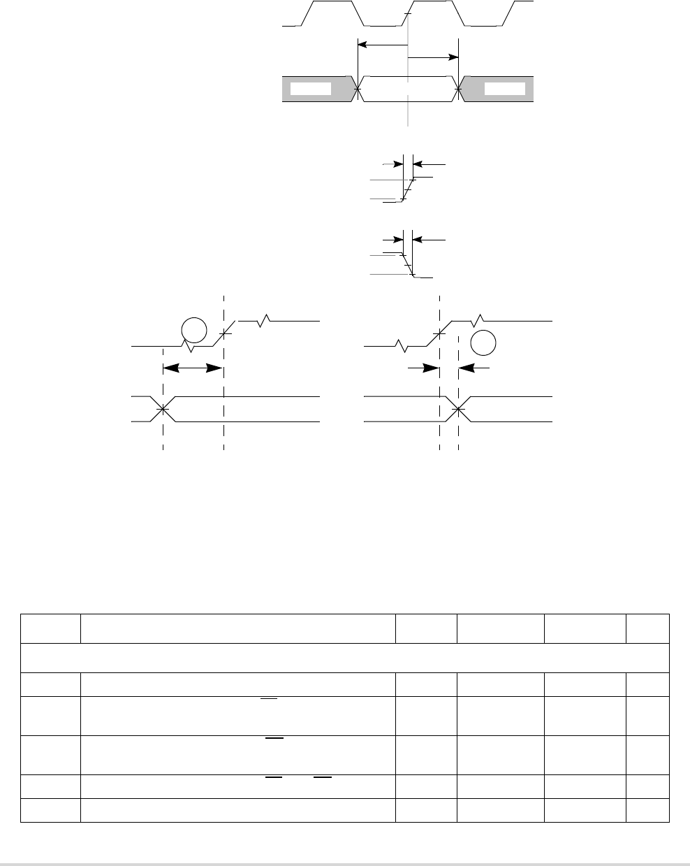
MOTOROLA Chapter 33. Electrical Characteristics 33-11
Processor Bus Output Timing Specifications
Timings listed in Table 33-10 are shown in Figure 33-1.
Figure 33-1. General Input Timing Requirements
33.8 Processor Bus Output Timing Specifications
Table 33-10 lists processor bus output timings.
Table 33-11. External Bus Output Timing Specifications
Name Characteristic Symbol Min Max Unit
Control Outputs
B6a CLKOUT high to chip selects valid 1tCHCV —0.5t
CYC +10 ns
B6b CLKOUT high to byte enables (BS[3:0]) valid2tCHBV —0.5t
CYC +10 ns
B6c CLKOUT high to output enable (OE) valid3tCHOV —0.5t
CYC +10 ns
B7 CLKOUT high to control output (BS[3:0], OE) invalid tCHCOI 0.5tCYC + 2 — ns
B7a CLKOUT high to chip selects invalid tCHCI 0.5tCYC + 2 — ns
Invalid Invalid
CLKOUT(66.67 MHz)
TSETUP THOLD
Input Setup And Hold
1.5V
trise = 1.5 ns
Vh = VIH
Vl = VIL
1.5V1.5V Valid
tfall = 1.5 ns
Vh = VIH
Vl = VIL
Input Rise Time
Input Fall Time
* The timings are also valid for inputs sampled on the negative clock edge.
Inputs
CLKOUT B4
B5
33-12 MCF5282 User’s Manual MOTOROLA
Processor Bus Output Timing Specifications
Read/write bus timings listed in Table 33-11 are shown in Figure 33-2, Figure 33-3, and
Figure 33-4.
Address and Attribute Outputs
B8 CLKOUT high to address (A[23:0]) and control (TS,
SIZ[1:0], TIP
, R/W) valid
tCHAV —10ns
B9 CLKOUT high to address (A[23:0]) and control (TS,
SIZ[1:0], TIP
, R/W) invalid
tCHAI 2—ns
Data Outputs
B11 CLKOUT high to data output (D[31:0]) valid tCHDOV —10ns
B12 CLKOUT high to data output (D[31:0]) invalid tCHDOI 2—ns
B13 CLKOUT high to data output (D[31:0]) high impedance tCHDOZ —6ns
1 CSn transitions after the falling edge of CLKOUT.
2 BS transitions after the falling edge of CLKOUT.
3 OE transitions after the falling edge of CLKOUT.
Table 33-11. External Bus Output Timing Specifications (Continued)
Name Characteristic Symbol Min Max Unit
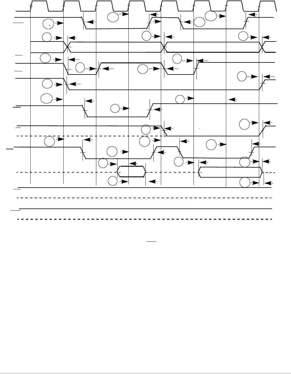
MOTOROLA Chapter 33. Electrical Characteristics 33-13
Processor Bus Output Timing Specifications
Figure 33-2. Read/Write (Internally Terminated) Timing
Figure 33-3 shows a bus cycle terminated by TA showing timings listed in Table 33-11.
CLKOUT
CSn
A[23:0]
R/W
BS[3:0]
D[31:0]
TA
(H)
(H)
S0
S2 S3
S1 S4 S5 S0 S1 S2 S3 S4 S5
TEA (H)
B6a
B8
B7a
B6c
B7
B6b
B7
B4
B5
B11 B12
B9
B9
B8
B6b
B13
OE
B0
B7
B9
TS
TIP
B8
B8
B9
B8
B9
SIZ[1:0]
B7a
B6a
B8
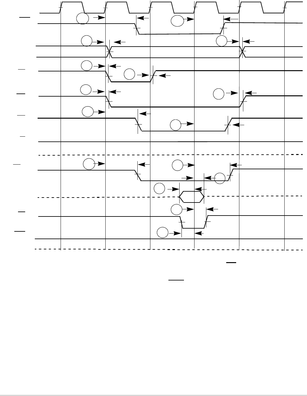
33-14 MCF5282 User’s Manual MOTOROLA
Processor Bus Output Timing Specifications
Figure 33-3. Read Bus Cycle Terminated by TA
Figure 33-4 shows a bus cycle terminated by TEA; it displays the timings listed in
Table 33-11.
CLKOUT
CSn
A[23:0]
OE
R/W
BS[3:0]
TA
(H)
S0 S2 S3
S1 S4 S5 S0 S1
TEA
(H)
B6a
B8
B7a
B9
B6c
B7
B6b B7
B2a
B1a
D[31:0]
B4
B5
B8
B9
TS
B9
TIP
B8
SIZ[1:0]
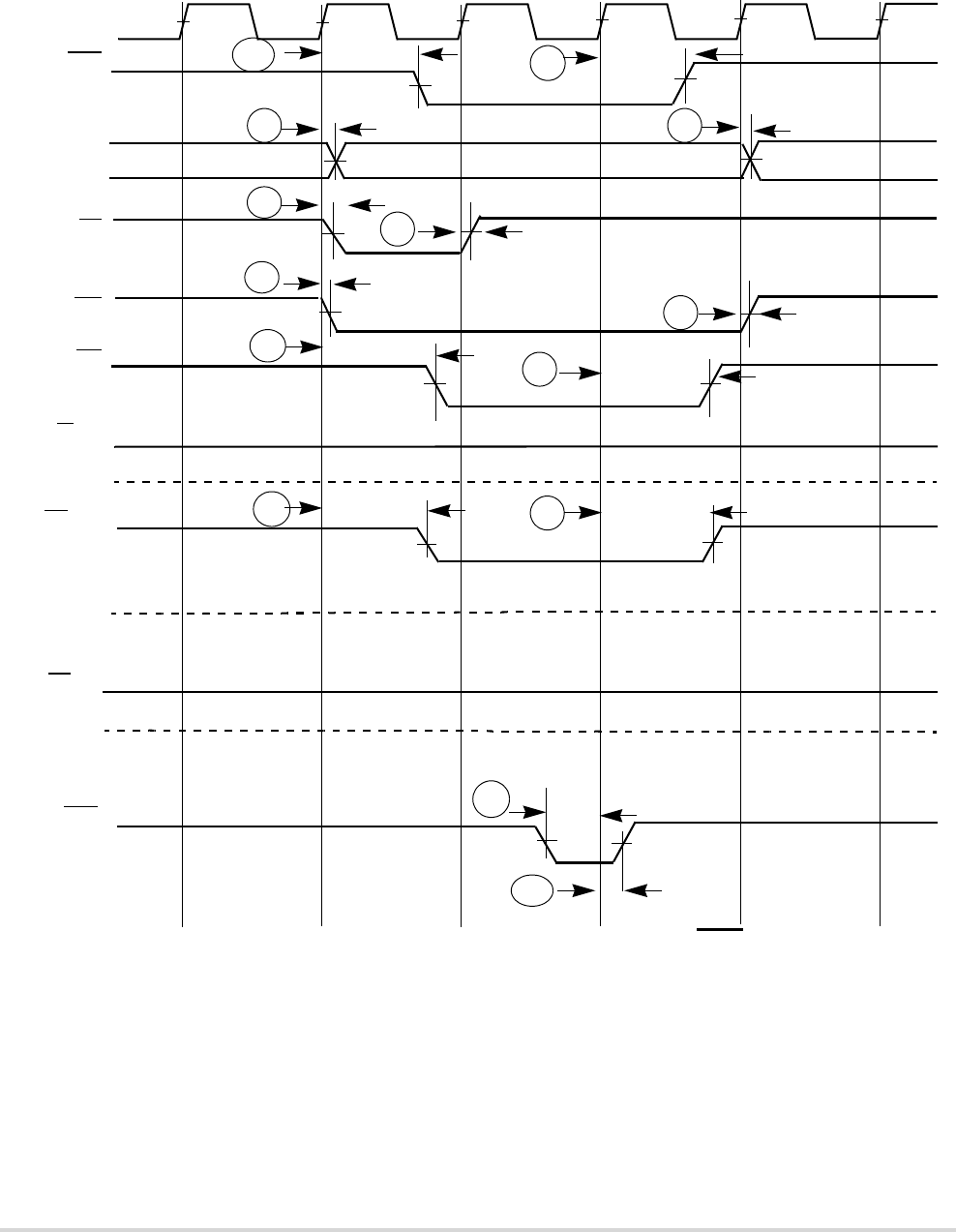
MOTOROLA Chapter 33. Electrical Characteristics 33-15
Processor Bus Output Timing Specifications
Figure 33-4. Read Bus Cycle Terminated by TEA
CLKOUT
CSn
A[23:0]
OE
R/W
BS[3:0]
TEA
(H)
S0
S2 S3
S1 S4 S5 S0 S1
TA
(H)
B6a
B8
B7a
B9
B6c
B7
B6b B7
B2a
B1a
D[31:0]
B8
B9
TS
B9
TIP
B8
SIZ[1:0]
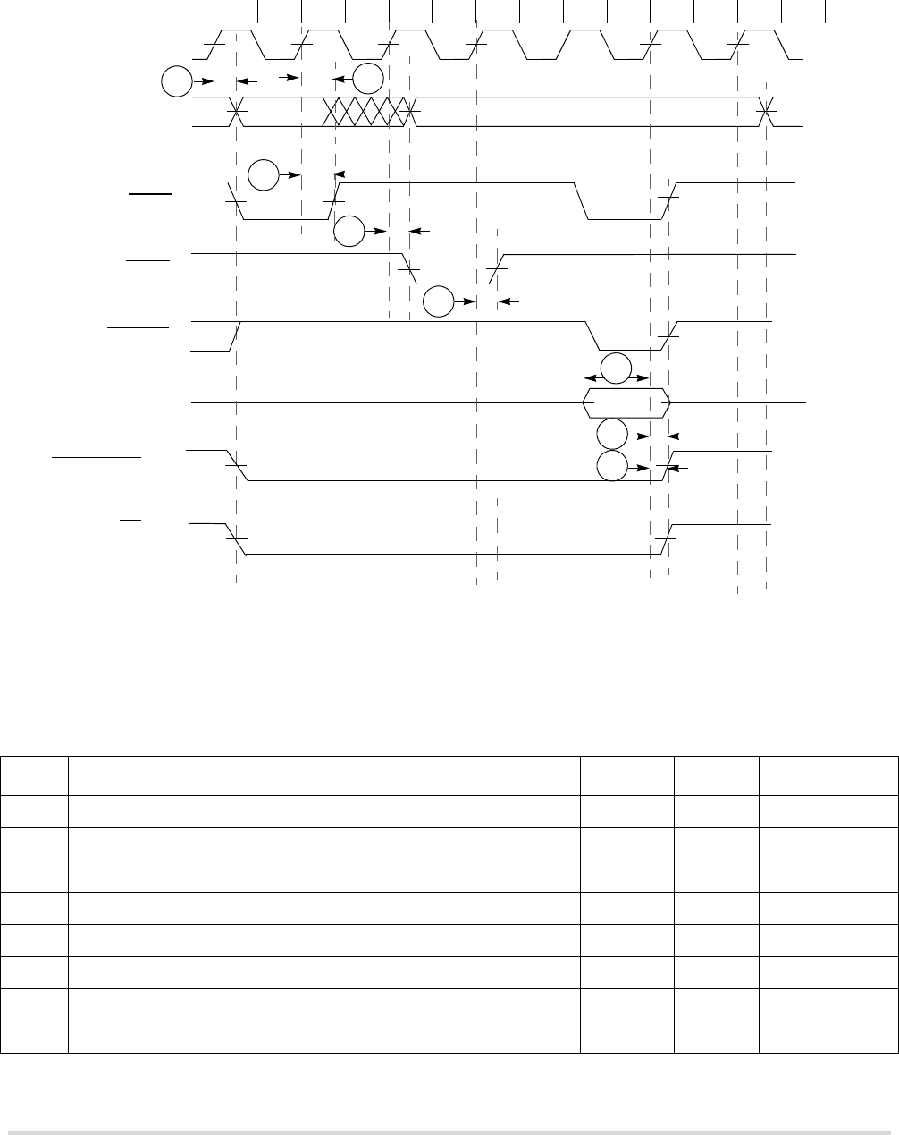
33-16 MCF5282 User’s Manual MOTOROLA
Processor Bus Output Timing Specifications
Figure 33-5 shows an SDRAM read cycle.
Figure 33-5. SDRAM Read Cycle
Table 33-12. SDRAM Timing
NUM Characteristic1
1All timing specifications are based on taking into account, a 25pF load on the SDRAM output pins.
Symbol Min Max Unit
D1 CLKOUT high to SDRAM address valid tCHDAV —10ns
D2 CLKOUT high to SDRAM control valid tCHDCV —10ns
D3 CLKOUT high to SDRAM address invalid tCHDAI 2—ns
D4 CLKOUT high to SDRAM control invalid tCHDCI 2—ns
D5 SDRAM data valid to CLKOUT high tDDVCH 6—ns
D6 CLKOUT high to SDRAM data invalid tCHDDI 1—ns
D72
2D7 and D8 are for write cycles only.
CLKOUT high to SDRAM data valid tCHDDVW —10ns
D82CLKOUT high to SDRAM data invalid tCHDDIW 2—ns
A[23:0]
SRAS
D[31:0]
ACTV NOP
SDRAM_CS[1:0]
READ
Column
CLKOUT
0
DRAMW
BS[3:0]
12345678910 11 12 13
D1
D2
D4
D6
D5
D4
1 DACR[CASL] = 2
SCAS 1
NOP
D4
Row
D3
PRE
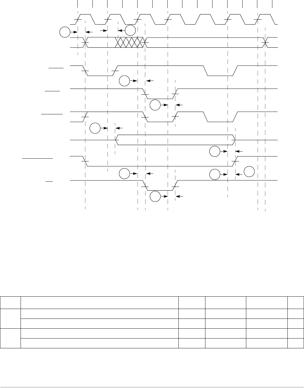
MOTOROLA Chapter 33. Electrical Characteristics 33-17
General Purpose I/O Timing
Figure 33-6 shows an SDRAM write cycle.
Figure 33-6. SDRAM Write Cycle
33.9 General Purpose I/O Timing
Table 33-13. GPIO Timing1, 2
(VDD = 2.7 to 3.6 V, VSS = 0 V, VDDH = 5 V)
NUM Characteristic Symbol Min Max Unit
G1
G2
CLKOUT High to GPIO Output Valid tCHPOV —12ns
CLKOUT High to GPIO Output Invalid tCHPOI 2—ns
G3
G4
GPIO Input Valid to CLKOUT High tPVCH 10 — ns
CLKOUT High to GPIO Input Invalid tCHPI 2—ns
A[23:0]
SRAS
SCAS1
D[31:0]
ACTV PALLNOP
SDRAM_CS[1:0]
WRITE
Row Column
CLKOUT
DRAMW
BS[3:0]
D1
D2
D4
D8
D4
012345678910 11 12
D7
NOP
1 DACR[CASL] = 2
D4
D3
D2
D4
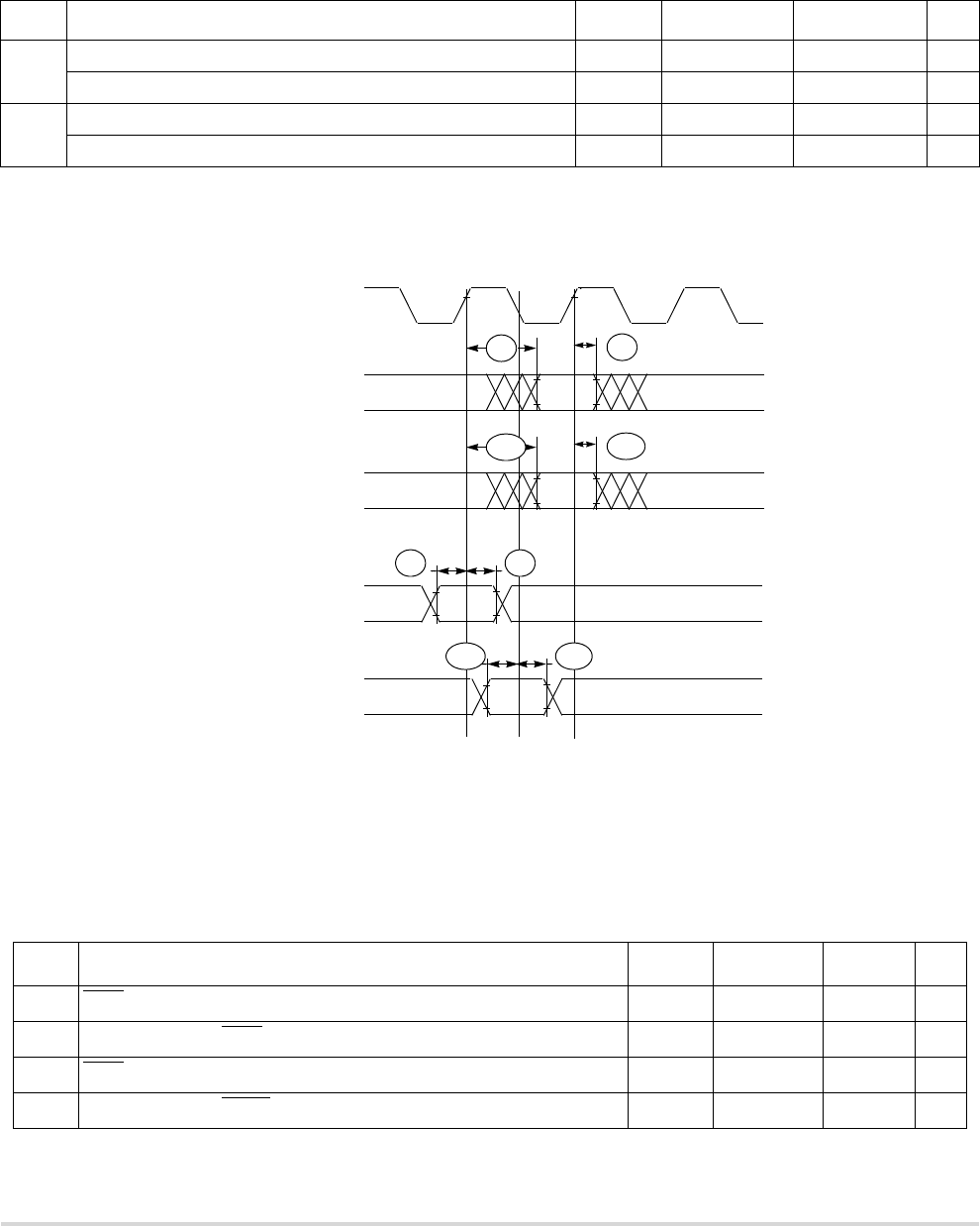
33-18 MCF5282 User’s Manual MOTOROLA
Reset and Configuration Override Timing
Figure 33-7. GPIO Timing
33.10 Reset and Configuration Override Timing
G1a
G2a
CLKOUT High to PQA/PQB Output Valid tCHPAOV —12ns
CLKOUT High to PQA/PQB Output Invalid tCHPAOI 2—ns
G3a
G4a
PQA/PQB Input Valid to CLKOUT Low tPAVCH 10 — ns
CLKOUT Low to PQA/PQB Input Invalid tCHPAI 2—ns
1GPIO pins include: Ports A-I, INT, SPI, SCI1/2 (including SCI functions), FlexCAN and Timer.
2Because of long delays associated with the PQA/PQB pads, signals on the PQA/PQB pins will be updated on the
following edge of the clock.
Table 33-14. Reset and Configuration Override Timing
(VDD = 2.7 to 3.6 V, VSS = 0 V)1
NUM Characteristic Symbol Min Max Unit
R1 RSTI Input valid to CLKOUT High tRVCH 10 — ns
R2 CLKOUT High to RSTI Input invalid tCHRI 2—ns
R3 RSTI Input valid Time 2tRIVT 5—t
CYC
R4 CLKOUT High to RSTO Valid tCHROV —12ns
Table 33-13. GPIO Timing1, 2 (Continued)
(VDD = 2.7 to 3.6 V, VSS = 0 V, VDDH = 5 V)
NUM Characteristic Symbol Min Max Unit
G1
CLKOUT
GPIO Outputs
G2
PQA/PQB Outputs
G2a
G3a G4a
PQA/PQB Inputs
G3 G4
GPIO Inputs
G1a
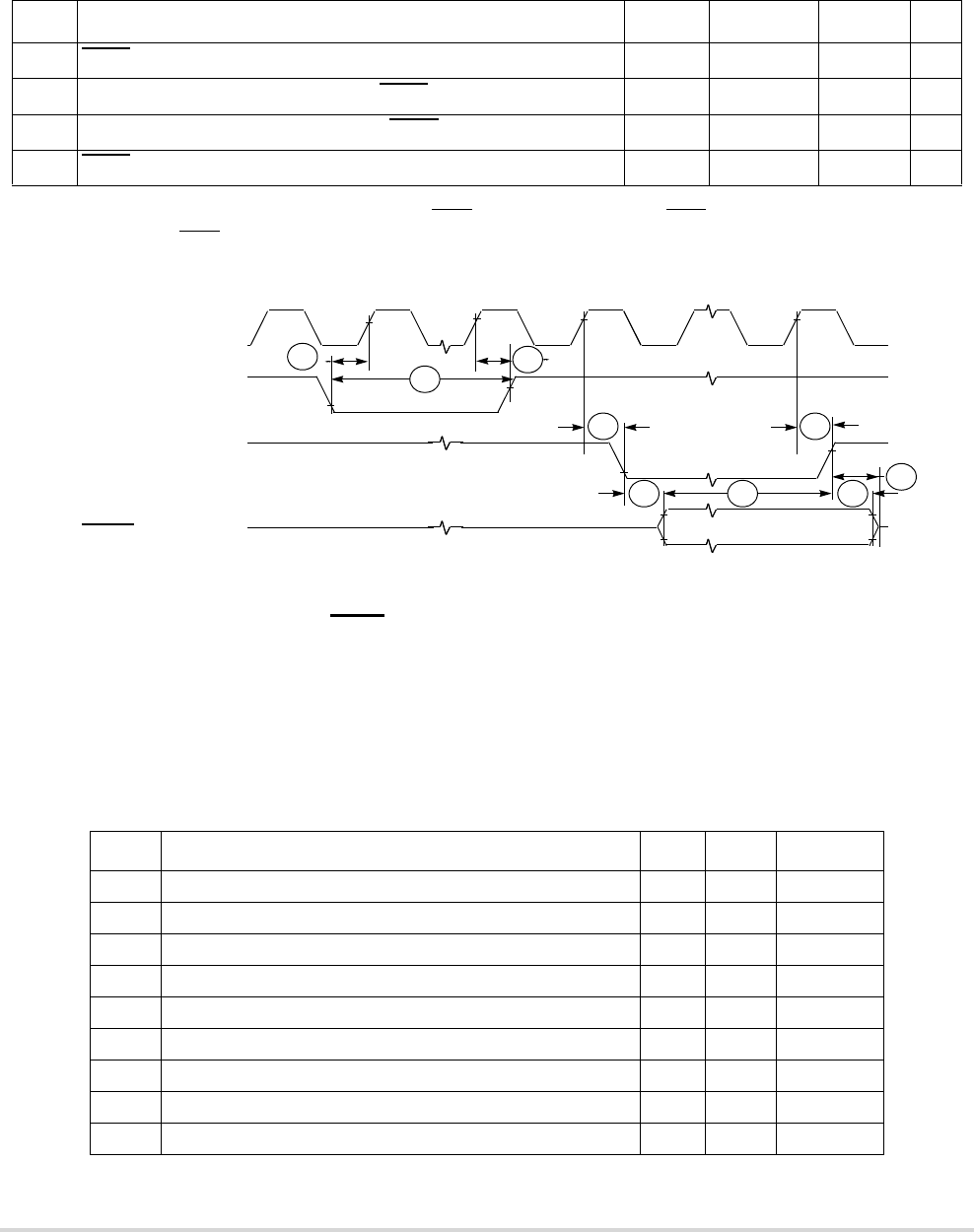
MOTOROLA Chapter 33. Electrical Characteristics 33-19
I2C Input/Output Timing Specifications
Figure 33-8. RSTI and Configuration Override Timing
33.11 I2C Input/Output Timing Specifications
Table 33-15 lists specifications for the I2C input timing parameters shown in Figure 33-9.
R5 RSTO valid to Config. Overrides valid tROVCV 0—ns
R6 Configuration Override Setup Time to RSTO invalid tCOS 20 — tCYC
R7 Configuration Override Hold Time after RSTO invalid tCOH 0—ns
R8 RSTO invalid to Configuration Override High Impedance tROICZ —1t
CYC
1All AC timing is shown with respect to 50% VDD levels unless otherwise noted.
2During low-power STOP, the synchronizers for the RSTI input are bypassed and RSTI is asserted asynchronously to
the system. Thus, RSTI must be held a minimum of 100 ns.
Table 33-15. I2C Input Timing Specifications between SCL and SDA
Num Characteristic Min Max Units
I1 Start condition hold time 2 — Bus clocks
I2 Clock low period 8 — Bus clocks
I3 SCL/SDA rise time (VIL = 0.5 V to VIH =2.4 V) — 1 mS
I4 Data hold time 0 — ns
I5 SCL/SDA fall time (VIH = 2.4 V to VIL = 0.5 V) — 1 mS
I6 Clock high time 4 — Bus clocks
I7 Data setup time 0 — ns
I8 Start condition setup time (for repeated start condition only) 2 — Bus clocks
I9 Stop condition setup time 2 — Bus clocks
Table 33-14. Reset and Configuration Override Timing (Continued)
(VDD = 2.7 to 3.6 V, VSS = 0 V)1
NUM Characteristic Symbol Min Max Unit
R1 R2
CLKOUT
RSTI
RSTO
R3
R4
R8
R7R6R5
Configuration Overrides:
R4
(RCON, Override pins)
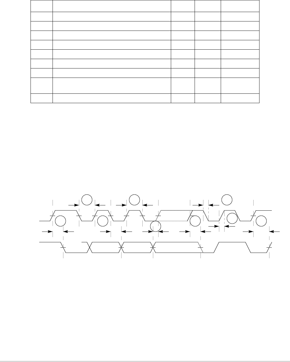
33-20 MCF5282 User’s Manual MOTOROLA
Fast Ethernet AC Timing Specifications
Table 33-16 lists specifications for the I2C output timing parameters shown in Figure 33-9.
Figure 33-9 shows timing for the values in Table 33-15 and Table 33-16.
Figure 33-9. I2C Input/Output Timings
33.12 Fast Ethernet AC Timing Specifications
MII signals use TTL signal levels compatible with devices operating at either 5.0 V or
3.3 V.
Table 33-16. I2C Output Timing Specifications between SCL and SDA
Num Characteristic Min Max Units
I11
1Note: Output numbers depend on the value programmed into the IFDR; an IFDR programmed
with the maximum frequency (IFDR = 0x20) results in minimum output timings as shown in
Table 33-16. The I2C interface is designed to scale the actual data transition time to move it to
the middle of the SCL low period. The actual position is affected by the prescale and division
values programmed into the IFDR; however, the numbers given in Table 33-16 are minimum
values.
Start condition hold time 6 — Bus clocks
I2 1 Clock low period 10 — Bus clocks
I3 2
2Because SCL and SDA are open-collector-type outputs, which the processor can only actively
drive low, the time SCL or SDA take to reach a high level depends on external signal
capacitance and pull-up resistor values.
SCL/SDA rise time (VIL = 0.5 V to VIH = 2.4 V) — — µS
I4 1Data hold time 7 — Bus clocks
I5 3
3Specified at a nominal 50-pF load.
SCL/SDA fall time (VIH = 2.4 V to VIL = 0.5 V) — 3 ns
I6 1Clock high time 10 — Bus clocks
I7 1Data setup time 2 — Bus clocks
I8 1Start condition setup time (for repeated start
condition only)
20 — Bus clocks
I9 1Stop condition setup time 10 — Bus clocks
I2 I6
I1 I4
I7
I8 I9
I5
I3
SCL
SDA
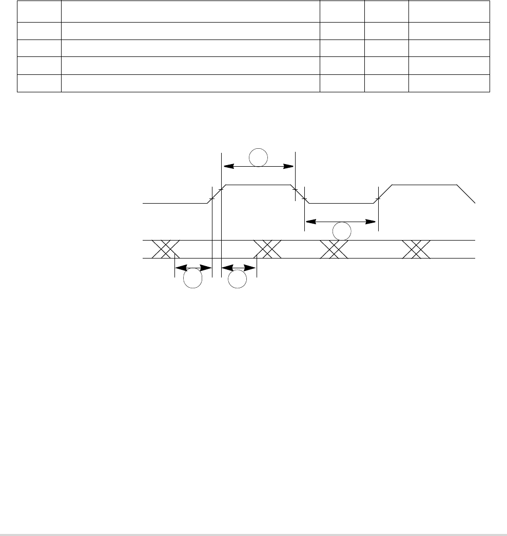
MOTOROLA Chapter 33. Electrical Characteristics 33-21
Fast Ethernet AC Timing Specifications
33.12.1 MII Receive Signal Timing (ERXD[3:0], ERXDV,
ERXER, and ERXCLK)
The receiver functions correctly up to a ERXCLK maximum frequency of 25 MHz +1%.
There is no minimum frequency requirement. In addition, the processor clock frequency
must exceed twice the ERXCLK frequency.
Table 33-17 lists MII receive channel timings.
Figure 33-10 shows MII receive signal timings listed in Table 33-17.
Figure 33-10. MII Receive Signal Timing Diagram
33.12.2 MII Transmit Signal Timing (ETXD[3:0], ETXEN,
ETXER, ETXCLK)
The transmitter functions correctly up to a ETXCLK maximum frequency of 25 MHz +1%.
There is no minimum frequency requirement. In addition, the processor clock frequency
must exceed twice the ETXCLK frequency.
The transmit outputs (ETXD[3:0], ETXEN, ETXER) can be programmed to transition
from either the rising or falling edge of ETXCLK, and the timing is the same in either case.
This options allows the use of non-compliant MII PHYs. Refer to the Ethernet chapter for
details of this option and how to enable it.
Table 33-17. MII Receive Signal Timing
Num Characteristic 1
1ERXDV, ERXCLK, and ERXD[0] have same timing in 10 Mbps 7-wire interface mode.
Min Max Unit
M1 ERXD[3:0], ERXDV, ERXER to ERXCLK setup 5 — ns
M2 ERXCLK to ERXD[3:0], ERXDV, ERXER hold 5 — ns
M3 ERXCLK pulse width high 35% 65% ERXCLK period
M4 ERXCLK pulse width low 35% 65% ERXCLK period
M1 M2
ERXCLK (input)
ERXD[3:0] (inputs)
ERXDV
ERXER
M3
M4
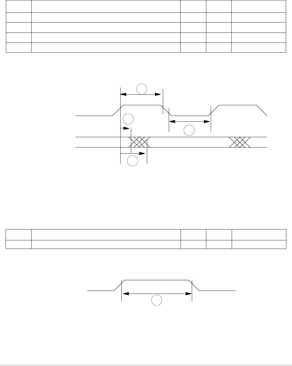
33-22 MCF5282 User’s Manual MOTOROLA
Fast Ethernet AC Timing Specifications
Table 33-18 lists MII transmit channel timings.
Figure 33-11 shows MII transmit signal timings listed in Table 33-18.
Figure 33-11. MII Transmit Signal Timing Diagram
33.12.3 MII Async Inputs Signal Timing (ECRS and ECOL)
Table 33-19 lists MII asynchronous inputs signal timing.
Figure 33-12 shows MII asynchronous input timings listed in Table 33-19.
Figure 33-12. MII Async Inputs Timing Diagram
Table 33-18. MII Transmit Signal Timing
Num Characteristic1
1ETXCLK, ETXD0, and ETXEN have the same timing in 10 Mbit 7-wire interface mode.
Min Max Unit
M5 ETXCLK to ETXD[3:0], ETXEN, ETXER invalid 5 — ns
M6 ETXCLK to ETXD[3:0], ETXEN, ETXER valid — 25 ns
M7 ETXCLK pulse width high 35% 65% ETXCLK period
M8 ETXCLK pulse width low 35% 65% ETXCLK period
Table 33-19. MII Async Inputs Signal Timing
Num Characteristic Min Max Unit
M91
1ECOL has the same timing in 10 Mbit 7-wire interface mode.
ECRS, ECOL minimum pulse width 1.5 — ETXCLK period
M6
ETXCLK (input)
ETXD[3:0] (outputs)
ETXEN
ETXER
M5
M7
M8
ECRS, ECOL
M9
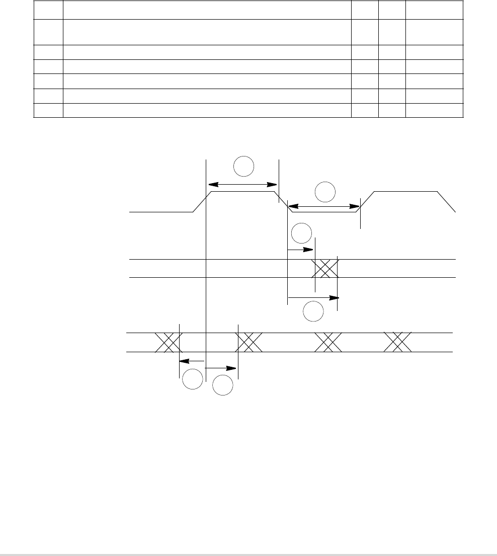
MOTOROLA Chapter 33. Electrical Characteristics 33-23
Fast Ethernet AC Timing Specifications
33.12.4 MII Serial Management Channel Timing
(EMDIO and EMDC)
The FEC functions correctly with a maximum MDC frequency of 2.5 MHz.
Table 33-20 lists MII serial management channel timings.
Figure 33-13 shows MII serial management channel timings listed in Table 33-20.
Figure 33-13. MII Serial Management Channel Timing Diagram
Table 33-20. MII Serial Management Channel Timing
Num Characteristic Min Max Unit
M10 EMDC falling edge to EMDIO output invalid (minimum propagation
delay)
0— ns
M11 EMDC falling edge to EMDIO output valid (max prop delay) — 25 ns
M12 EMDIO (input) to EMDC rising edge setup 10 — ns
M13 EMDIO (input) to EMDC rising edge hold 0 — ns
M14 EMDC pulse width high 40% 60% MDC period
M15 EMDC pulse width low 40% 60% MDC period
M11
EMDC (output)
EMDIO (output)
M12 M13
EMDIO (input)
M10
M14
M15
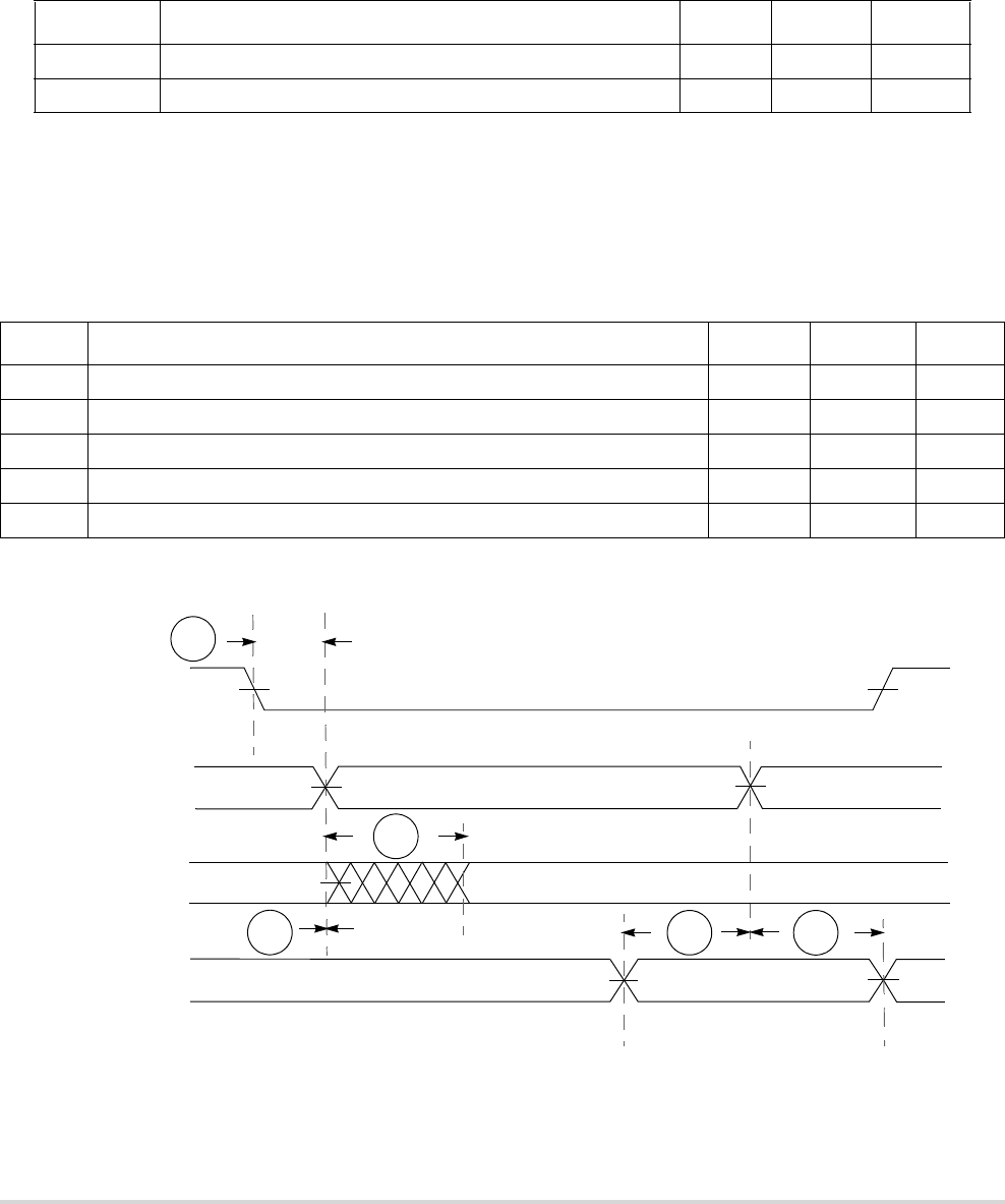
33-24 MCF5282 User’s Manual MOTOROLA
DMA Timer Module AC Timing Specifications
33.13 DMA Timer Module AC Timing Specifications
Table 33-21 lists timer module AC timings.
33.14 QSPI Electrical Specifications
Table 33-22 lists QSPI timings.
The values in Table 33-22 correspond to Figure 33-14.
Figure 33-14. QSPI Timing
Table 33-21. Timer Module AC Timing Specifications
Name Characteristic 1
1All timing references to CLKOUT are given to its rising edge when bit 3 of the SDRAM control register is 0.
Min Max Unit
T1 DTIN0 / DTIN1 / DTIN2 / DTIN3 cycle time 3 — tCYC
T2 DTIN0 / DTIN1 / DTIN2 / DTIN3 pulse width 1 — tCYC
Table 33-22. QSPI Modules AC Timing Specifications
Name Characteristic Min Max Unit
QS1 QSPI_CS[3:0] to QSPI_CLK 1 × tcyc 510 × tcyc ns
QS2 QSPI_CLK high to QSPI_DOUT valid. — 12 ns
QS3 QSPI_CLK high to QSPI_DOUT invalid. (Output hold) 2 — ns
QS4 QSPI_DIN to QSPI_CLK (Input setup) 10 — ns
QS5 QSPI_DIN to QSPI_CLK (Input hold) 10 — ns
QSPI_CS[3:0]
QSPI_CLK
QSPI_DOUT
QS5
QS1
QSPI_DIN
QS3 QS4
QS2
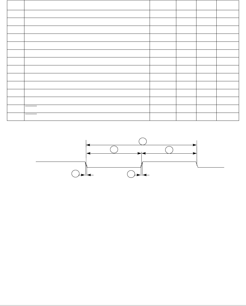
MOTOROLA Chapter 33. Electrical Characteristics 33-25
JTAG and Boundary Scan Timing
33.15 JTAG and Boundary Scan Timing
Figure 33-15. Test Clock Input Timing
Table 33-23. JTAG and Boundary Scan Timing
Num Characteristics1
1JTAG_EN is expected to be a static signal. Hence, it is not associated with any timing
Symbol Min Max Unit
1 TCLK Frequency of Operation fJCYC DC 1/4 fsys
2 TCLK Cycle Period tJCYC 4—t
CYC
3 TCLK Clock Pulse Width tJCW 25.0 — ns
4 TCLK Rise and Fall Times tJCRF 0.0 3.0 ns
5 Boundary Scan Input Data Setup Time to TCLK Rise tBSDST 5.0 — ns
6 Boundary Scan Input Data Hold Time after TCLK Rise tBSDHT 25.0 — ns
7 TCLK Low to Boundary Scan Output Data Valid tBSDV 0.0 30.0 ns
8 TCLK Low to Boundary Scan Output High Z tBSDZ 0.0 30.0 ns
9 TMS, TDI Input Data Setup Time to TCLK Rise tTAPBST 5.0 — ns
10 TMS, TDI Input Data Hold Time after TCLK Rise tTAPBHT 10.0 — ns
11 TCLK Low to TDO Data Valid tTDODV 0.0 25.0 ns
12 TCLK Low to TDO High Z tTDODZ 0.0 8.0 ns
13 TRST Assert Time tTRSTAT 100.0 — ns
14 TRST Setup Time (Negation) to TCLK High tTRSTST 10.0 — ns
TCLK
VIL
VIH
33
44
2
(input)
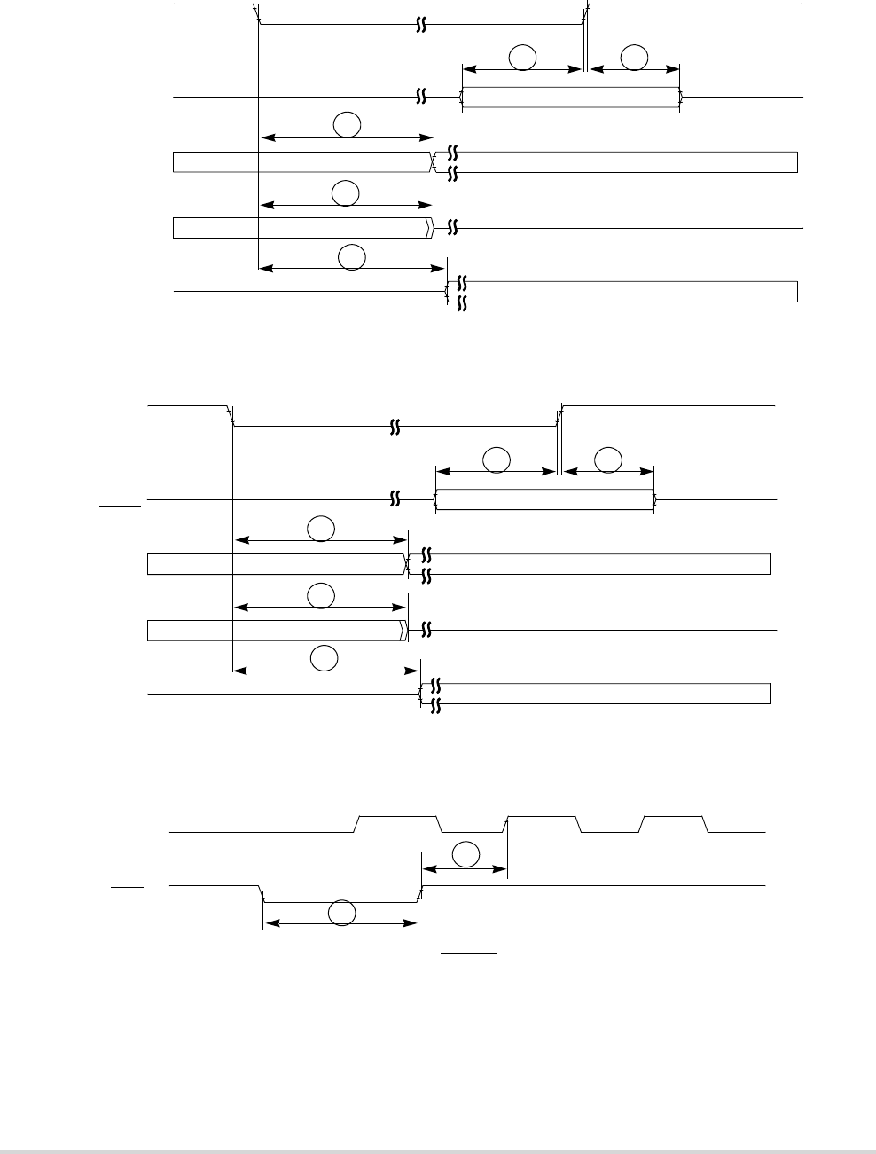
33-26 MCF5282 User’s Manual MOTOROLA
JTAG and Boundary Scan Timing
Figure 33-16. Boundary Scan (JTAG) Timing
Figure 33-17. Test Access Port Timing
Figure 33-18. TRST Timing
Input Data Valid
Output Data Valid
Output Data Valid
TCLK
Data Inputs
Data Outputs
Data Outputs
Data Outputs
VIL VIH
56
7
8
7
Input Data Valid
Output Data Valid
Output Data Valid
TCLK
TDI
TDO
TDO
TDO
TMS
VIL VIH
910
11
12
11
BKPT
TCLK
TRST
14
13
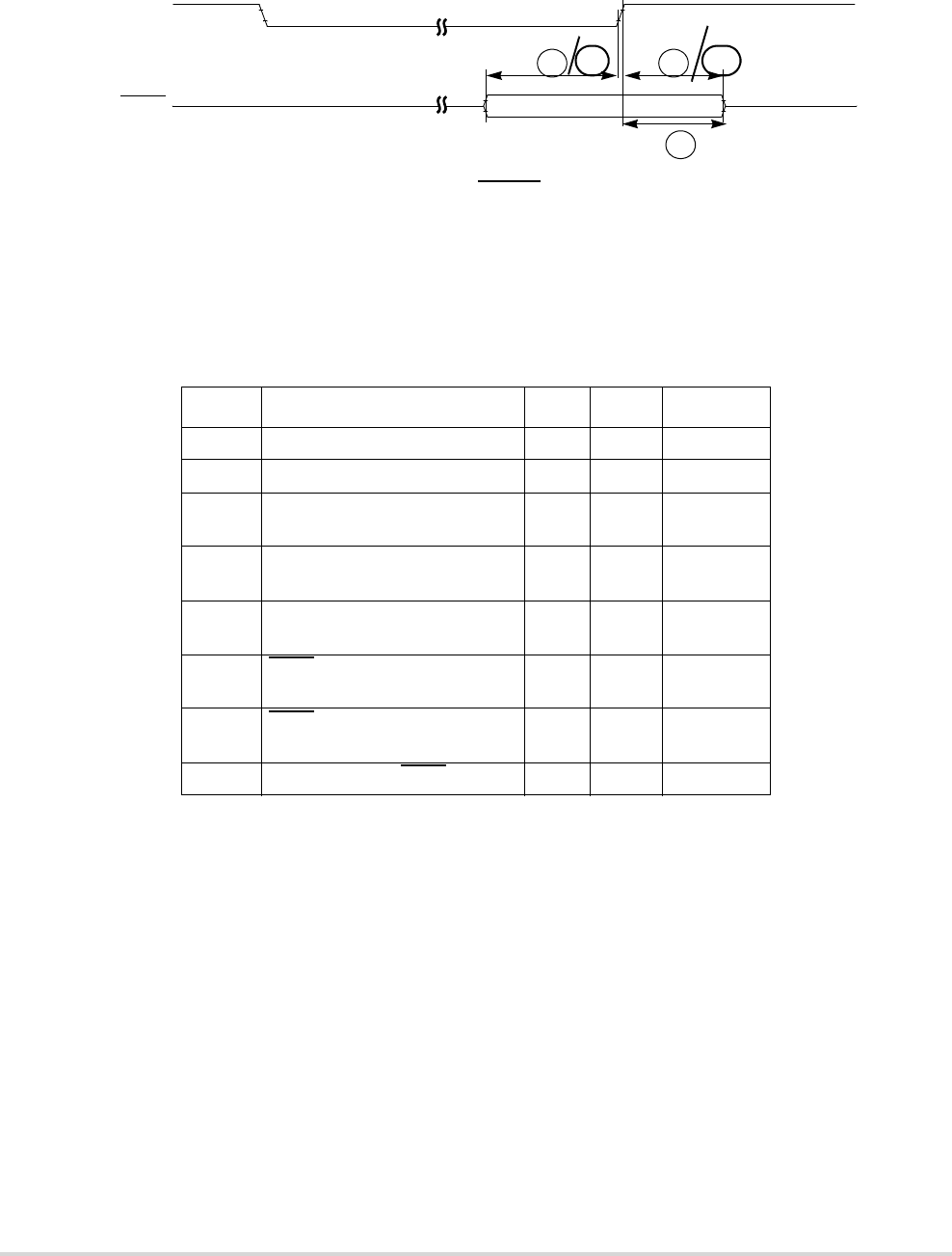
MOTOROLA Chapter 33. Electrical Characteristics 33-27
Debug AC Timing Specifications
Figure 33-19. BKPT Timing
33.16 Debug AC Timing Specifications
Table 33-24 lists specifications for the debug AC timing parameters shown in Figure 33-21.
Table 33-24. Debug AC Timing Specification
Num Characteristic Min Max Units
D1 PST, DDATA to TCLK setup 5 ns
D2 TCLK to PST, DDATA hold 2 ns
D3 DSI-to-DSCLK setup 1 CLKOUT
cycles
D4 1
1DSCLK and DSI are synchronized internally. D4 is measured from the
synchronized DSCLK input relative to the rising edge of CLKOUT.
DSCLK-to-DSO hold 4 CLKOUT
cycles
D5 DSCLK cycle time 5 CLKOUT
cycles
D6 BKPT input data setup time to
CLKOUT Rise
5.0 ns
D7 BKPT input data hold time to
CLKOUT Rise
2.0 ns
D8 CLKOUT high to BKPT high Z 0.0 10.0 ns
Input Data Valid
CLKOUT
BKPT
(Input)
VIL VIH
15 16
B1b
B2b
17
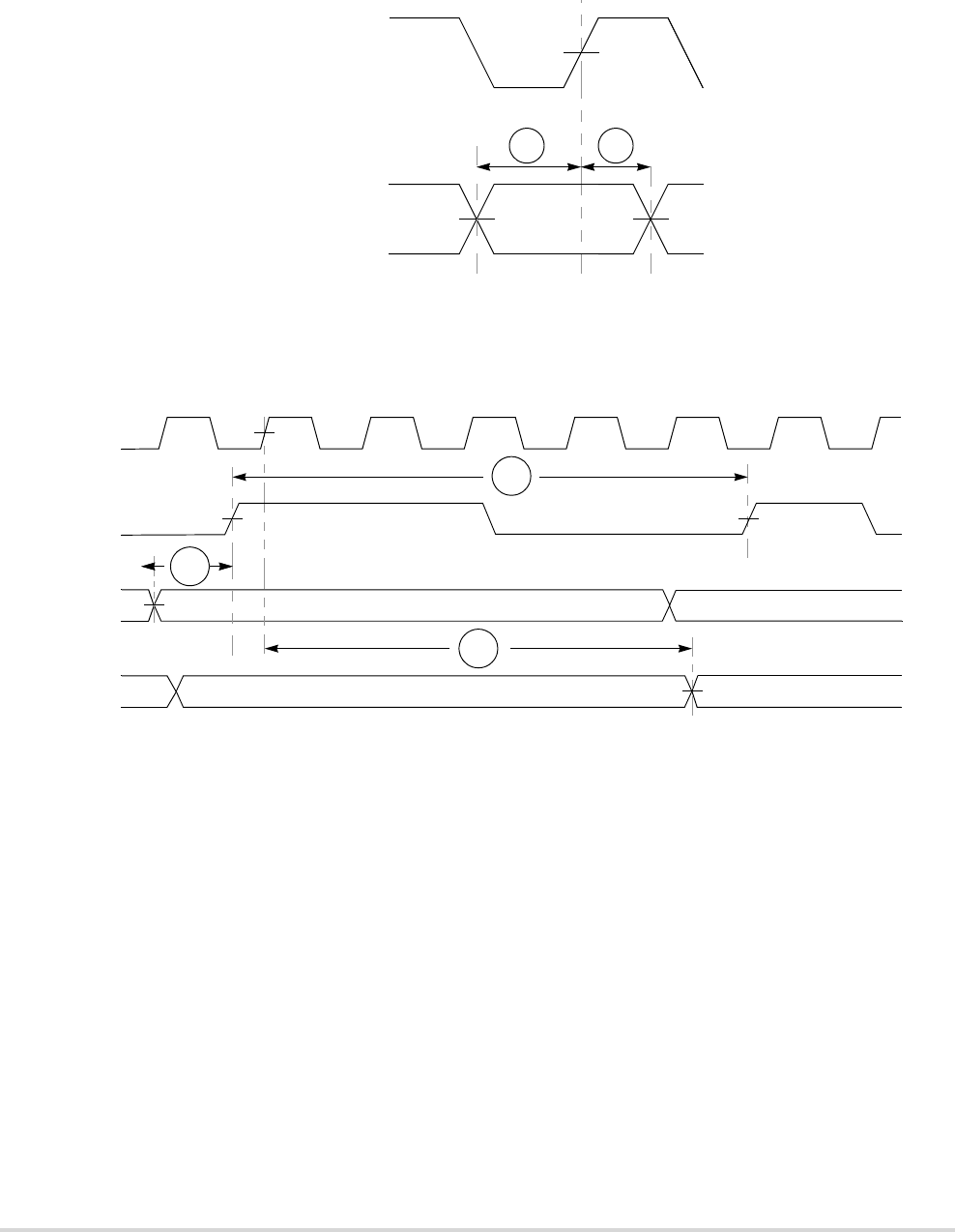
33-28 MCF5282 User’s Manual MOTOROLA
Debug AC Timing Specifications
Figure 33-20 shows real-time trace timing for the values in Table 33-24.
Figure 33-20. Real-Time Trace AC Timing
Figure 33-21 shows BDM serial port AC timing for the values in Table 33-24.
Figure 33-21. BDM Serial Port AC Timing
CLKOUT
PST[3:0]
D2D1
DDATA[3:0]
DSI
DSO
Current Next
CLKOUT
Past Current
DSCLK
D3
D4
D5

MOTOROLA Appendix A. Register Memory Map A-1
Appendix A
Register Memory Map
Table A-1 summarizes the address, name, and byte assignment for registers within the
MCF5282 CPU space. Table A-2 lists an overview of the memory map for the on-chip
modules, and Table A-3 is a detailed memory map including all of the registers for on-chip
modules.
Table A-1. CPU Space Register Memory Map
Address Name Mnemonic Size
CPU @ 0x002 Cache Control Register CACR 32
CPU @ 0x004 Access Control Register 0 ACR0 32
CPU @ 0x005 Access Control Register 1 ACR1 32
CPU @ 0x800 Other Stack Pointer OTHER_A7 32
CPU @ 0x801 Vector Base Register VBR 32
CPU @ 0x804 MAC Status Register MACSR 8
CPU @ 0x805 MAC Mask Register MASK 16
CPU @ 0x806 MAC Accumulator 0 ACC0 16
CPU @ 0x807 MAC Accumulator 0, 1 extension bytes ACCext01 16
CPU @ 0x808 MAC Accumulator 2, 3 extension bytes ACCext23 16
CPU @ 0x809 MAC Accumulator 1 ACC1 16
CPU @ 0x80A MAC Accumulator 2 ACC2 16
CPU @ 0x80B MAC Accumulator 3 ACC3 16
CPU @ 0x80E Status Register SR 16
CPU @ 0x80F Program Counter PC 32
CPU @ 0xC04 Flash Base Address Register FLASHBAR 32
CPU @ 0xC05 RAM Base Address Register RAMBAR 32

A-2 MCF5282 User’s Manual MOTOROLA
Table A-2. Module Memory Map Overview
Address Module Size
IPSBAR + 0x00_0000 System Control Module 64 bytes
IPSBAR + 0x00_0040 SDRAM Controller 64 bytes
IPSBAR + 0x00_0080 Chip Selects 128 bytes
IPSBAR + 0x00_0100 DMA (Channel 0) 64 bytes
IPSBAR + 0x00_0140 DMA (Channel 1) 64 bytes
IPSBAR + 0x00_0180 DMA (Channel 2) 64 bytes
IPSBAR + 0x00_01C0 DMA (Channel 3) 64 bytes
IPSBAR + 0x00_0200 UART0 64 bytes
IPSBAR + 0x00_0240 UART1 64 bytes
IPSBAR + 0x00_0280 UART2 64 bytes
IPSBAR + 0x00_0300 I2C 64 bytes
IPSBAR + 0x00_0340 QSPI 64 bytes
IPSBAR + 0x00_0400 DMA Timer 0 64 bytes
IPSBAR + 0x00_0440 DMA Timer 1 64 bytes
IPSBAR + 0x00_0480 DMA Timer 2 64 bytes
IPSBAR + 0x00_04C0 DMA Timer 3 64 bytes
IPSBAR + 0x00_0C00 Interrupt Controller 0 256 bytes
IPSBAR + 0x00_0D00 Interrupt Controller 1 256 bytes
IPSBAR + 0x00_0F00 Global Interrupt Acknowledge Cycles 256 bytes
IPSBAR + 0x00_1000 Fast Ethernet Controller (Registers and MIB RAM) 1 K
IPSBAR + 0x00_1400 Fast Ethernet Controller (FIFO Memory) 1K
IPSBAR + 0x10_0000 Ports 64K
IPSBAR + 0x11_0000 Reset Controller, Chip Configuration, and Power Management 64K
IPSBAR + 0x12_0000 Clock Module 64K
IPSBAR + 0x13_0000 Edge Port 64K
IPSBAR + 0x14_0000 Watchdog Timer 64K
IPSBAR + 0x15_0000 Programmable Interval Timer 0 64K
IPSBAR + 0x16_0000 Programmable Interval Timer 1 64K
IPSBAR + 0x17_0000 Programmable Interval Timer 2 64K
IPSBAR + 0x18_0000 Programmable Interval Timer 3 64K
IPSBAR + 0x19_0000 QADC 64K
IPSBAR + 0x1A_0000 General Purpose Timer A 64K
IPSBAR + 0x1B_0000 General Purpose Timer B 64K
IPSBAR + 0x1C_0000 FlexCAN 64K
IPSBAR + 0x1D_0000 CFM (Flash) Control Registers 64K
IPSBAR + 0x400_0000 CFM (Flash) Memory for IPS Reads and Writes 512K

MOTOROLA Appendix A. Register Memory Map A-3
Table A-3. Register Memory Map
Address Name Mnemonic Size
SCM Registers
IPSBAR + 0x000 Internal Peripheral System Base Address Register IPSBAR 32
IPSBAR + 0x008 Copy of RAMBAR RAMBAR 32
IPSBAR + 0x00C Reserved —
IPSBAR + 0x010 Core Reset Status Register CRSR 8
IPSBAR + 0x011 Core Watchdog Control Register CWCR 8
IPSBAR + 0x012 Low-Power Interrupt Control Register LPICR 8
IPSBAR + 0x013 Core Watchdog Service Register CWSR 8
IPSBAR + 0x014 DMA Request Control Register DMAREQC 32
IPSBAR + 0x01C Bus Master Park Register MPARK 32
IPSBAR + 0x020 Master Privilege Register MPR 32
IPSBAR + 0x024 Peripheral Access Control Register 0 PACR0 8
IPSBAR + 0x025 Peripheral Access Control Register 1 PACR1 8
IPSBAR + 0x026 Peripheral Access Control Register 2 PACR2 8
IPSBAR + 0x027 Peripheral Access Control Register 3 PACR3 8
IPSBAR + 0x028 Peripheral Access Control Register 4 PACR4 8
IPSBAR + 0x02A Peripheral Access Control Register 5 PACR5 8
IPSBAR + 0x02B Peripheral Access Control Register 6 PACR6 8
IPSBAR + 0x02C Peripheral Access Control Register 7 PACR7 8
IPSBAR + 0x02E Peripheral Access Control Register 8 PACR8 8
IPSBAR + 0x030 Grouped Peripheral Access Control Register 0 GPACR0 8
IPSBAR + 0x031 Grouped Peripheral Access Control Register 1 GPACR1 8
SDRAMC Registers
IPSBAR + 0x040 DRAM Control Register DCR 16
IPSBAR + 0x048 DRAM Address and Control Register 0 DACR0 32
IPSBAR + 0x04C DRAM Mask Register Block 0 DMR0 32
IPSBAR + 0x050 DRAM Address and Control Register 1 DACR1 32
IPSBAR + 0x054 DRAM Mask Register Block 1 DMR1 32
Chip Select Registers
IPSBAR + 0x080 Chip Select Address Register 0 CSAR0 16
IPSBAR + 0x084 Chip Select Mask Register 0 CSMR0 32
IPSBAR + 0x08A Chip Select Control Register 0 CSCR0 16
IPSBAR + 0x08C Chip Select Address Register 1 CSAR1 16
IPSBAR + 0x092 Chip Select Mask Register 1 CSMR1 32
IPSBAR + 0x094 Chip Select Control Register 1 CSCR1 16

A-4 MCF5282 User’s Manual MOTOROLA
IPSBAR + 0x098 Chip Select Address Register 2 CSAR2 16
IPSBAR + 0x09C Chip Select Mask Register 2 CSMR2 32
IPSBAR + 0x0A2 Chip Select Control Register 2 CSCR2 16
IPSBAR + 0x0A4 Chip Select Address Register 2 CSAR3 16
IPSBAR + 0x0A8 Chip Select Mask Register 3 CSMR3 32
IPSBAR + 0x0AE Chip Select Control Register 3 CSCR3 16
IPSBAR + 0x0B0 Chip Select Address Register 4 CSAR4 16
IPSBAR + 0x0B4 Chip Select Mask Register 4 CSMR4 32
IPSBAR + 0x0BA Chip Select Control Register 4 CSCR4 16
IPSBAR + 0x0BC Chip Select Address Register 5 CSAR5 16
IPSBAR + 0x0C0 Chip Select Mask Register 5 CSMR5 32
IPSBAR + 0x0C6 Chip Select Control Register 5 CSCR5 16
IPSBAR + 0x0C8 Chip Select Address Register 6 CSAR6 16
IPSBAR + 0x0CC Chip Select Mask Register 6 CSMR6 32
IPSBAR + 0x0D2 Chip Select Control Register 6 CSCR6 16
DMA Registers
IPSBAR + 0x100 Source Address Register 0 SAR0 32
IPSBAR + 0x104 Destination Address Register 0 DAR0 32
IPSBAR + 0x108 DMA Control Register 0 DCR0 32
IPSBAR + 0x10C Byte Count Register 0 BCR01 32
IPSBAR + 0x110 DMA Status Register 0 DSR0 8
IPSBAR + 0x140 Source Address Register 1 SAR1 32
IPSBAR + 0x144 Destination Address Register 1 DAR1 32
IPSBAR + 0x148 DMA Control Register 1 DCR1 32
IPSBAR + 0x14C Byte Count Register 1 BCR1132
IPSBAR + 0x150 DMA Status Register 1 DSR1 8
IPSBAR + 0x180 Source Address Register 2 SAR2 32
IPSBAR + 0x184 Destination Address Register 2 DAR2 32
IPSBAR + 0x188 DMA Control Register 2 DCR2 32
IPSBAR + 0x18C Byte Count Register 2 BCR2132
IPSBAR + 0x190 DMA Status Register 2 DSR2 8
IPSBAR + 0x1C0 Source Address Register 3 SAR3 32
IPSBAR + 0x1C4 Destination Address Register 3 DAR3 32
IPSBAR + 0x1C8 DMA Control Register 3 DCR3 32
IPSBAR + 0x1CC Byte Count Register 3 BCR3132
Table A-3. Register Memory Map (Continued)
Address Name Mnemonic Size

MOTOROLA Appendix A. Register Memory Map A-5
IPSBAR + 0x1D0 DMA Status Register 3 DSR3 8
UART Registers
IPSBAR + 0x200 UART Mode Register 02UMR10,
UMR20
8
IPSBAR + 0x204 (Read) UART Status Register 0 USR0 8
(Write) UART Clock Select Register 01UCSR0 8
IPSBAR + 0x208 (Read) Reserved 8
(Write) UART Command Register 0 UCR0 8
IPSBAR + 0x20C (Read) UART Receive Buffer 0 URB0 8
(Write) UART Transmit Buffer 0 UTB0 8
IPSBAR + 0x210 (Read) UART Input Port Change Register 0 UIPCR0 8
(Write) UART Auxiliary Control Register 01UACR0 8
IPSBAR + 0x214 (Read) UART Interrupt Status Register 0 UISR0 8
(Write) UART Interrupt Mask Register 0 UIMR0 8
IPSBAR + 0x218 (Read) Reserved38
UART Baud Rate Generator Register 10 UBG10 8
IPSBAR + 0x21C (Read) Reserved38
UART Baud Rate Generator Register 20 UBG20 8
IPSBAR + 0x234 (Read) UART Input Port Register 0 UIP0 8
(Write) Reserved38
IPSBAR + 0x238 (Read) Reserved38
(Write) UART Output Port Bit Set Command
Register 0
UOP10 8
IPSBAR + 0x23C (Read) Reserved38
(Write) UART Output Port Bit Reset Command
Register 0
UIP00 8
IPSBAR + 0x240 UART Mode Registers 12UMR11,
UMR21
8
IPSBAR + 0x244 (Read) UART Status Register 1 USR1 8
(Write) UART Clock Select Register 11UCSR1 8
IPSBAR + 0x248 (Read) Reserved38
(Write) UART Command Register 1 UCR1 8
IPSBAR + 0x24C (UART/Read) UART Receive Buffer 1 URB1 8
(UART/Write) UART Transmit Buffer 1 UTB1 8
IPSBAR + 0x250 (Read) UART Input Port Change Register 1 UIPCR1 8
(Write) UART Auxiliary Control Register 11UACR1 8
Table A-3. Register Memory Map (Continued)
Address Name Mnemonic Size

A-6 MCF5282 User’s Manual MOTOROLA
IPSBAR + 0x254 (Read) UART Interrupt Status Register 1 UISR1 8
(Write) UART Interrupt Mask Register 1 UIMR1 8
IPSBAR + 0x258 (Read) Reserved38
UART Baud Rate Generator Register 11 UBG11 8
IPSBAR + 0x25C (Read) Reserved38
UART Baud Rate Generator Register 21 UBG21 8
IPSBAR + 0x274 (Read) UART Input Port Register 1 UIP1 8
(Write) Reserved38
IPSBAR + 0x278 (Read) Reserved38
(Write) UART Output Port Bit Set Command
Register 1
UOP11 8
IPSBAR + 0x27C (Read) Reserved38
(Write) UART Output Port Bit Reset Command
Register 1
UIP01 8
IPSBAR + 0x280 UART Mode Register 22UMR12,
UMR22
8
IPSBAR + 0x284 (Read) UART Status Register 2 USR2 8
(Write) UART Clock Select Register 21UCSR2 8
IPSBAR + 0x288 (Read) Reserved38
(Write) UART Command Register 2 UCR2 8
IPSBAR + 0x28C (Read) UART Receive Buffer 2 URB2 8
(Write) UART Transmit Buffer 2 UTB2 8
IPSBAR + 0x290 (Read) UART Input Port Change Register 2 UIPCR2 8
(Write) UART Auxiliary Control Register 21UACR2 8
IPSBAR + 0x294 (Read) UART Interrupt Status Register 2 UISR2 8
(Write) UART Interrupt Mask Register 2 UIMR2 8
IPSBAR + 0x298 (Read) Reserved38
UART Baud Rate Generator Register 12 UBG12 8
IPSBAR + 0x29C (Read) Reserved38
UART Baud Rate Generator Register 22 UBG22 8
IPSBAR + 0x2B4 (Read) UART Input Port Register 2 UIP2 8
(Write) Reserved38
IPSBAR + 0x2B8 (Read) Reserved38
(Write) UART Output Port Bit Set Command
Register 2
UOP12 8
Table A-3. Register Memory Map (Continued)
Address Name Mnemonic Size

MOTOROLA Appendix A. Register Memory Map A-7
IPSBAR + 0x2BC (Read) Reserved38
(Write) UART Output Port Bit Reset Command
Register 2
UIP02 8
I2C Registers
IPSBAR + 0x300 I2C Address Register I2ADR 8
IPSBAR + 0x304 I2C Frequency Divider Register I2FDR 8
IPSBAR + 0x308 I2C Control Register I2CR 8
IPSBAR + 0x30C I2C Status Register I2SR 8
IPSBAR + 0x310 I2C Data I/O Register I2DR 8
QSPI Registers
IPSBAR + 0x340 QSPI Mode Register QMR 16
IPSBAR + 0x344 QSPI Delay Register QDLYR 16
IPSBAR + 0x348 QSPI Wrap Register QWR 16
IPSBAR + 0x34C QSPI Interrupt Register QIR 16
IPSBAR + 0x350 QSPI Address Register QAR 16
IPSBAR + 0x354 QSPI Data Register QDR 16
DMA Timer Registers
IPSBAR + 0x400 DMA Timer Mode Register 0 DTMR0 16
IPSBAR + 0x402 DMA Timer Extended Mode Register 0 DTXMR0 8
IPSBAR + 0x403 DMA Timer Event Register 0 DTER0 8
IPSBAR + 0x404 DMA Timer Reference Register 0 DTRR0 32
IPSBAR + 0x408 DMA Timer Capture Register 0 DTCR0 32
IPSBAR + 0x40C DMA Timer Counter Register 0 DTCN0 32
IPSBAR + 0x440 DMA Timer Mode Register 1 DTMR1 16
IPSBAR + 0x442 DMA Timer Extended Mode Register 1 DTXMR1 8
IPSBAR + 0x443 DMA Timer Event Register 1 DTER1 8
IPSBAR + 0x444 DMA Timer Reference Register 1 DTRR1 32
IPSBAR + 0x448 DMA Timer Capture Register 1 DTCR1 32
IPSBAR + 0x44C DMA Timer Counter Register 1 DTCN1 32
IPSBAR + 0x480 DMA Timer Mode Register 2 DTMR2 16
IPSBAR + 0x482 DMA Timer Extended Mode Register 2 DTXMR2 8
IPSBAR + 0x483 DMA Timer Event Register 2 DTER2 8
IPSBAR + 0x484 DMA Timer Reference Register 2 DTRR2 32
IPSBAR + 0x488 DMA Timer Capture Register 2 DTCR2 32
IPSBAR + 0x48C DMA Timer Counter Register 2 DTCN2 32
Table A-3. Register Memory Map (Continued)
Address Name Mnemonic Size

A-8 MCF5282 User’s Manual MOTOROLA
IPSBAR + 0x4C0 DMA Timer Mode Register 3 DTMR3 16
IPSBAR + 0x4C2 DMA Timer Extended Mode Register 3 DTXMR3 8
IPSBAR + 0x4C3 DMA Timer Event Register 3 DTER3 8
IPSBAR + 0x4C4 DMA Timer Reference Register 3 DTRR3 32
IPSBAR + 0x4C8 DMA Timer Capture Register 3 DTCR3 32
IPSBAR + 0x4CC DMA Timer Counter Register 3 DTCN3 32
Interrupt Controller 0
IPSBAR + 0xC00 Interrupt Pending Register High 0 IPRH0 32
IPSBAR + 0xC04 Interrupt Pending Register Low 0 IPRL0 32
IPSBAR + 0xC08 Interrupt Mask Register High 0 IMRH0 32
IPSBAR + 0xC0C Interrupt Mask Register Low 0 IMRL0 32
IPSBAR + 0xC10 Interrupt Force Register High 0 INTFRCH0 32
IPSBAR + 0xC14 Interrupt Force Register Low 0 INTFRCL0 32
IPSBAR + 0xC18 Interrupt Level Request Register 0 ILRR0 8
IPSBAR + 0XC19 Interrupt Acknowledge Level and Priority Register 0 IACKLPR0 8
IPSBAR + 0xC41 Interrupt Control Register 0-01 ICR001 8
IPSBAR + 0xC42 Interrupt Control Register 0-02 ICR002 8
IPSBAR + 0xC43 Interrupt Control Register 0-03 ICR003 8
IPSBAR + 0xC44 Interrupt Control Register 0-04 ICR004 8
IPSBAR + 0xC45 Interrupt Control Register 0-05 ICR005 8
IPSBAR + 0xC46 Interrupt Control Register 0-06 ICR006 8
IPSBAR + 0xC47 Interrupt Control Register 0-07 ICR007 8
IPSBAR + 0xC48 Interrupt Control Register 0-08 ICR008 8
IPSBAR + 0xC49 Interrupt Control Register 0-09 ICR009 8
IPSBAR + 0xC4A Interrupt Control Register 0-10 ICR010 8
IPSBAR + 0xC4B Interrupt Control Register 0-11 ICR011 8
IPSBAR + 0xC4C Interrupt Control Register 0-12 ICR012 8
IPSBAR + 0xC4D Interrupt Control Register 0-13 ICR013 8
IPSBAR + 0xC4E Interrupt Control Register 0-14 ICR014 8
IPSBAR + 0xC4F Interrupt Control Register 0-15 ICR015 8
IPSBAR + 0xC51 Interrupt Control Register 0-17 ICR017 8
IPSBAR + 0xC52 Interrupt Control Register 0-18 ICR018 8
IPSBAR +0xC53 Interrupt Control Register 0-19 ICR019 8
IPSBAR + 0xC54 Interrupt Control Register 0-20 ICR020 8
IPSBAR + 0xC55 Interrupt Control Register 0-21 ICR021 8
Table A-3. Register Memory Map (Continued)
Address Name Mnemonic Size

MOTOROLA Appendix A. Register Memory Map A-9
IPSBAR + 0xC56 Interrupt Control Register 0-22 ICR022 8
IPSBAR + 0xC57 Interrupt Control Register 0-23 ICR023 8
IPSBAR + 0xC58 Interrupt Control Register 0-24 ICR024 8
IPSBAR + 0xC59 Interrupt Control Register 0-25 ICR025 8
IPSBAR + 0xC5A Interrupt Control Register 0-26 ICR026 8
IPSBAR + 0xC5B Interrupt Control Register 0-27 ICR027 8
IPSBAR + 0xC5C Interrupt Control Register 0-28 ICR028 8
IPSBAR + 0xC5D Interrupt Control Register 0-29 ICR029 8
IPSBAR + 0xC5E Interrupt Control Register 0-30 ICR030 8
IPSBAR + 0xC5F Interrupt Control Register 0-31 ICR031 8
IPSBAR + 0xC60 Interrupt Control Register 0-32 ICR032 8
IPSBAR + 0xC61 Interrupt Control Register 0-33 ICR033 8
ISPBAR + 0xC62 Interrupt Control Register 0-34 ICR034 8
IPSBAR + 0xC63 Interrupt Control Register 0-35 ICR035 8
IPSBAR + 0xC64 Interrupt Control Register 0-36 ICR036 8
IPSBAR + 0xC65 Interrupt Control Register 0-37 ICR037 8
IPSBAR + 0xC66 Interrupt Control Register 0-38 ICR038 8
IPSBAR + 0xC67 Interrupt Control Register 0-39 ICR039 8
IPSBAR + 0xC68 Interrupt Control Register 0-40 ICR040 8
IPSBAR + 0xC69 Interrupt Control Register 0-41 ICR041 8
IPSBAR + 0xC6A Interrupt Control Register 0-42 ICR042 8
IPSBAR + 0xC6B Interrupt Control Register 0-43 ICR043 8
IPSBAR + 0xC6C Interrupt Control Register 0-44 ICR044 8
IPSBAR + 0xC6D Interrupt Control Register 0-45 ICR45 8
IPSBAR + 0xC6E Interrupt Control Register 0-46 ICR046 8
IPSBAR + 0xC6F Interrupt Control Register 0-47 ICR047 8
IPSBAR + 0xC70 Interrupt Control Register 0-48 ICR048 8
IPSBAR + 0xC71 Interrupt Control Register 0-49 ICR049 8
IPSBAR + 0xC72 Interrupt Control Register 0-50 ICR050 8
IPSBAR + 0xC73 Interrupt Control Register 0-51 ICR051 8
IPSBAR + 0xC74 Interrupt Control Register 0-52 ICR052 8
IPSBAR + 0xC75 Interrupt Control Register 0-53 ICR053 8
IPSBAR + 0xC76 Interrupt Control Register 0-54 ICR054 8
IPSBAR + 0xC77 Interrupt Control Register 0-55 ICR055 8
IPSBAR + 0xC78 Interrupt Control Register 0-56 ICR056 8
Table A-3. Register Memory Map (Continued)
Address Name Mnemonic Size

A-10 MCF5282 User’s Manual MOTOROLA
IPSBAR + 0xC79 Interrupt Control Register 0-57 ICR057 8
IPSBAR + 0xC7A Interrupt Control Register 0-58 ICR058 8
IPSBAR + 0xC7B Interrupt Control Register 0-59 ICR059 8
IPSBAR + 0xC7C Interrupt Control Register 0-60 ICR060 8
IPSBAR + 0xC7D Interrupt Control Register 0-61 ICR061 8
IPSBAR + 0xC7E Interrupt Control Register 0-62 ICR062 8
IPSBAR + 0xCE0 Software Interrupt Acknowledge Register 0 SWACKR0 8
IPSBAR + 0xCE4 Level 1 Interrupt Acknowledge Register 0 L1IACKR0 8
IPSBAR + 0xCE8 Level 2 Interrupt Acknowledge Register 0 L2IACKR0 8
IPSBAR + 0xCEC Level 3 Interrupt Acknowledge Register 0 L3IACKR0 8
IPSBAR + 0xCF0 Level 4 Interrupt Acknowledge Register 0 L4IACKR0 8
IPSBAR + 0xCF4 Level 5 Interrupt Acknowledge Register 0 L5IACKR0 8
IPSBAR + 0xCF8 Level 6 Interrupt Acknowledge Register 0 L6IACKR0 8
IPSBAR + 0xCFC Level 7 Interrupt Acknowledge Register 0 L7IACKR0 8
Interrupt Controller 1
IPSBAR + 0xD00 Interrupt Pending Register High 1 IPRH1 32
IPSBAR + 0xD04 Interrupt Pending Register Low 1 IPRL1 32
IPSBAR + 0xD08 Interrupt Mask Register High 1 IMRH1 32
IPSBAR + 0xD0C Interrupt Mask Register Low 1 IMRL1 32
IPSBAR + 0xD10 Interrupt Force Register High 1 INTFRCH1 32
IPSBAR + 0xD14 Interrupt Force Register Low 1 INTFRCL1 32
IPSBAR + 0xD18 Interrupt Level Request Register 1 ILRR1 8
IPSBAR + 0xD19 Interrupt Acknowledge Level and Priority Register 1 IACKLPR1 8
IPSBAR + 0xD48 Interrupt Control Register 1-08 ICR108 8
IPSBAR + 0xD49 Interrupt Control Register 1-09 ICR109 8
IPSBAR + 0xD4A Interrupt Control Register 1-10 ICR110 8
IPSBAR + 0xD4B Interrupt Control Register 1-11 ICR111 8
IPSBAR + 0xD4C Interrupt Control Register 1-12 ICR112 8
IPSBAR + 0xD4D Interrupt Control Register 1-13 ICR113 8
IPSBAR + 0xD4E Interrupt Control Register 1-14 ICR114 8
IPSBAR + 0xD4F Interrupt Control Register 1-15 ICR115 8
IPSBAR + 0xD50 Interrupt Control Register 1-16 ICR116 8
IPSBAR + 0xD51 Interrupt Control Register 1-17 ICR117 8
IPSBAR + 0xD52 Interrupt Control Register 1-18 ICR118 8
IPSBAR + 0xD53 Interrupt Control Register 1-19 ICR119 8
Table A-3. Register Memory Map (Continued)
Address Name Mnemonic Size

MOTOROLA Appendix A. Register Memory Map A-11
IPSBAR + 0xD54 Interrupt Control Register 1-20 ICR120 8
IPSBAR + 0xD55 Interrupt Control Register 1-21 ICR121 8
IPSBAR + 0xD56 Interrupt Control Register 1-22 ICR122 8
IPSBAR + 0xD57 Interrupt Control Register 1-23 ICR123 8
IPSBAR + 0xD58 Interrupt Control Register 1-24 ICR124 8
IPSBAR + 0xD59 Interrupt Control Register 1-25 ICR125 8
IPSBAR + 0xD5A Interrupt Control Register 1-26 ICR126 8
IPSBAR + 0xDE0 Software Interrupt Acknowledge Register 1 SWACKR1 8
IPSBAR + 0xDE4 Level 1 Interrupt Acknowledge Register 1 L1IACKR1 8
IPSBAR + 0xDE8 Level 2 Interrupt Acknowledge Register 1 L2IACKR1 8
IPSBAR + 0xDEC Level 3 Interrupt Acknowledge Register 1 L3IACKR1 8
IPSBAR + 0xDF0 Level 4 Interrupt Acknowledge Register 1 L4IACKR1 8
IPSBAR + 0xDF4 Level 5 Interrupt Acknowledge Register 1 L5IACKR1 8
IPSBAR + 0xDF8 Level 6 Interrupt Acknowledge Register 1 L6IACKR1 8
IPSBAR + 0xDFC Level 7 Interrupt Acknowledge Register 1 L7IACKR1 8
Global Interrupt Acknowledge Cycle Registers
IPSBAR + 0xFE0 Global Software Interrupt Acknowledge Register GSWACKR 8
IPSBAR + 0xFE4 Global Level 1 Interrupt Acknowledge Register GL1IACKR 8
IPSBAR + 0xFE8 Global Level 2 Interrupt Acknowledge Register GL2IACKR 8
IPSBAR + 0xFEC Global Level 3 Interrupt Acknowledge Register GL3IACKR 8
IPSBAR + 0xFF0 Global Level 4 Interrupt Acknowledge Register GL4IACKR 8
IPSBAR + 0xFF4 Global Level 5 Interrupt Acknowledge Register GL5IACKR 8
IPSBAR + 0xFF8 Global Level 6 Interrupt Acknowledge Register GL6IACKR 8
IPSBAR + 0xFFC Global Level 7 Interrupt Acknowledge Register GL7IACKR 8
FEC Registers
IPSBAR + 0x1004 Interrupt Event Register EIR 32
IPSBAR + 0x1008 Interrupt Mask Register EIMR 32
IPSBAR + 0x1010 Receive Descriptor Active Register RDAR 32
IPSBAR + 0x1014 Transmit Descriptor Active Register XDAR 32
IPSBAR + 0x1024 Ethernet Control Register ECR 32
IPSBAR + 0x1040 MII Data Register MDATA 32
IPSBAR + 0x1044 MII Speed Control Register MSCR 32
IPSBAR + 0x1064 MIB Control/Status Register MIBC 32
IPSBAR + 0x1084 Receive Control Register RCR 32
IPSBAR + 0x10C4 Transmit Control Register TCR 32
Table A-3. Register Memory Map (Continued)
Address Name Mnemonic Size

A-12 MCF5282 User’s Manual MOTOROLA
IPSBAR + 0x10E4 Physical Address Low PALR 32
IPSBAR + 0x10E8 Physical Address High+ Type Field PAUR 32
IPSBAR + 0x10EC Opcode + Pause Duration OPD 32
IPSBAR + 0x1118 Upper 32 bits of individual hash table IAUR 32
IPSBAR + 0x111C Lower 32 bits of individual hash table IALR 32
IPSBAR + 0x1120 Upper 32-bits of group hash table GAUR 32
IPSBAR + 0x1124 Lower 32-bits of group hash table GALR 32
IPSBAR + 0x1144 Transmit FIFO Watermark TFWR 32
IPSBAR + 0x114C FIFO Receive Bound Register FRBR 32
IPSBAR + 0x1150 FIFO Receive Start Address FRSR 32
IPSBAR + 0x1180 Pointer to Receive Descriptor Ring ERDSR 32
IPSBAR + 0x1184 Pointer to Transmit Descriptor Ring ETDSR 32
IPSBAR + 0x1188 Maximum Receive Buffer Size EMRBR 32
IPSBAR +
0x1200-0x13FF
RAM used to store management counters MIB_RAM 32
GPIO Registers
IPSBAR +
0x10_0000
Port A Output Data Register PORTA 8
IPSBAR +
0x10_0001
Port B Output Data Register PORTB 8
IPSBAR +
0x10_0002
Port C Output Data Register PORTC 8
IPSBAR +
0x10_0003
Port D Output Data Register PORTD 8
IPSBAR +
0x10_0004
Port E Output Data Register PORTE 8
IPSBAR +
0x10_0005
Port F Output Data Register PORTF 8
IPSBAR +
0x10_0006
Port G Output Data Register PORTG 8
IPSBAR +
0x10_0007
Port H Output Data Register PORTH 8
IPSBAR +
0x10_0008
Port J Output Data Register PORTJ 8
IPSBAR +
0x10_0009
Port DD Output Data Register PORTDD 8
IPSBAR +
0x10_000A
Port EH Output Data Register PORTEH 8
IPSBAR +
0x10_000B
Port EL Output Data Register PORTEL 8
Table A-3. Register Memory Map (Continued)
Address Name Mnemonic Size

MOTOROLA Appendix A. Register Memory Map A-13
IPSBAR +
0x10_000C
Port AS Output Data Register PORTAS 8
IPSBAR +
0x10_000D
Port QS Output Data Register PORTQS 8
IPSBAR +
0x10_000E
Port SD Output Data Register PORTSD 8
IPSBAR +
0x10_000F
Port TC Output Data Register PORTTC 8
IPSBAR +
0x10_0010
Port TD Output Data Register PORTTD 8
IPSBAR +
0x10_0011
Port UA Output Data Register PORTUA 8
IPSBAR +
0x10_0014
Port A Data Direction Register DDRA 8
IPSBAR +
0x10_0015
Port B Data Direction Register DDRB 8
IPSBAR +
0x10_0016
Port C Data Direction Register DDRC 8
IPSBAR +
0x10_0017
Port D Data Direction Register DDRD 8
IPSBAR +
0x10_0018
Port E Data Direction Register DDRE 8
IPSBAR +
0x10_0019
Port F Data Direction Register DDRF 8
IPSBAR +
0x10_001A
Port G Data Direction Register DDRG 8
IPSBAR +
0x10_001B
Port H Data Direction Register DDRH 8
IPSBAR +
0x10_001C
Port J Data Direction Register DDRJ 8
IPSBAR +
0x10_001D
Port DD Data Direction Register DDRDD 8
IPSBAR +
0x10_001E
Port EH Data Direction Register DDREH 8
IPSBAR +
0x10_001F
Port EL Data Direction Register DDREL 8
IPSBAR +
0x10_0020
Port AS Data Direction Register DDRAS 8
IPSBAR +
0x10_0021
Port QS Data Direction Register DDRQS 8
IPSBAR +
0x10_0022
Port SD Data Direction Register DDRSD 8
Table A-3. Register Memory Map (Continued)
Address Name Mnemonic Size

A-14 MCF5282 User’s Manual MOTOROLA
IPSBAR +
0x10_0023
Port TC Data Direction Register DDRTC 8
IPSBAR +
0x10_0024
Port TD Data Direction Register DDRTD 8
IPSBAR +
0x10_0025
Port UA Data Direction Register DDRUA 8
IPSBAR +
0x10_0028
Port A Pin Data/Set Data Register PORTAP/
SETA
8
IPSBAR +
0x10_0029
Port B Pin Data/Set Data Register PORTBP/
SETB
8
IPSBAR +
0x10_002A
Port C Pin Data/Set Data Register PORTCP/
SETC
8
IPSBAR +
0x10_002B
Port D Pin Data/Set Data Register PORTDP/
SETD
8
IPSBAR +
0x10_002C
Port E Pin Data/Set Data Register PORTEP/
SETE
8
IPSBAR +
0x10_002D
Port F Pin Data/Set Data Register PORTFP/
SETF
8
IPSBAR +
0x10_002E
Port G Pin Data/Set Data Register PORTGP/
SETG
8
IPSBAR +
0x10_002F
Port H Pin Data/Set Data Register PORTHP/
SETH
8
IPSBAR +
0x10_0030
Port J Pin Data/Set Data Register PORTJP/
SETJ
8
IPSBAR +
0x10_0031
Port DD Pin Data/Set Data Register PORTDDP/
SETDD
8
IPSBAR +
0x10_0032
Port EH Pin Data/Set Data Register PORTEHP/
SETEH
8
IPSBAR +
0x10_0033
Port EL Pin Data/Set Data Register PORTELP/
SETEL
8
IPSBAR +
0x10_0034
Port AS Pin Data/Set Data Register PORTASP/
SETAS
8
IPSBAR +
0x10_0035
Port QS Pin Data/Set Data Register PORTQSP/
SETQS
8
IPSBAR +
0x10_0036
Port SD Pin Data/Set Data Register PORTSDP/
SETSD
8
IPSBAR +
0x10_0037
Port TC Pin Data/Set Data Register PORTTCP/
SETTC
8
IPSBAR +
0x10_0038
Port TD Pin Data/Set Data Register PORTTDP/
SETTD
8
IPSBAR +
0x10_0039
Port UA Pin Data/Set Data Register PORTUAP/
SETUA
8
Table A-3. Register Memory Map (Continued)
Address Name Mnemonic Size

MOTOROLA Appendix A. Register Memory Map A-15
IPSBAR +
0x10_003C
Port A Clear Output Data Register CLRA 8
IPSBAR +
0x10_003D
Port B Clear Output Data Register CLRB 8
IPSBAR +
0x10_003E
Port C Clear Output Data Register CLRC 8
IPSBAR +
0x10_003F
Port D Clear Output Data Register CLRD 8
IPSBAR +
0x10_0040
Port E Clear Output Data Register CLRE 8
IPSBAR +
0x10_0041
Port F Clear Output Data Register CLRF 8
IPSBAR +
0x10_0042
Port G Clear Output Data Register CLRG 8
IPSBAR +
0x10_0043
Port H Clear Output Data Register CLRH 8
IPSBAR +
0x10_0044
Port J Clear Output Data Register CLRJ 8
IPSBAR +
0x10_0045
Port DD Clear Output Data Register CLRDD 8
IPSBAR +
0x10_0046
Port EH Clear Output Data Register CLREH 8
IPSBAR +
0x10_0047
Port EL Clear Output Data Register CLREL 8
IPSBAR +
0x10_0048
Port AS Clear Output Data Register CLRAS 8
IPSBAR +
0x10_0049
Port QS Clear Output Data Register CLRQS 8
IPSBAR +
0x10_004A
Port SD Clear Output Data Register CLRSD 8
IPSBAR +
0x10_004B
Port TC Clear Output Data Register CLRTC 8
IPSBAR +
0x10_004C
Port TD Clear Output Data Register CLRTD 8
IPSBAR +
0x10_004D
Port UA Clear Output Data Register CLRUA 8
IPSBAR +
0x10_0050
Port B, C, and D Pin Assignment Register PBCDPAR 8
IPSBAR +
0x10_0051
Port F Pin Assignment Register PFPAR 8
IPSBAR +
0x10_0052
Port E Pin Assignment Register PEPAR 16
Table A-3. Register Memory Map (Continued)
Address Name Mnemonic Size

A-16 MCF5282 User’s Manual MOTOROLA
IPSBAR +
0x10_0054
Port J Pin Assignment Register PJPAR 8
IPSBAR +
0x10_0055
Port SD Pin Assignment Register PSDPAR 8
IPSBAR +
0x10_0056
Port AS Pin Assignment Register PASPAR 16
IPSBAR +
0x10_0058
Port EH and EL Pin Assignment Register PEHLPAR 8
IPSBAR +
0x10_0059
Port QS Pin Assignment Register PQSPAR 8
IPSBAR +
0x10_005A
Port TC Pin Assignment Register PTCPAR 8
IPSBAR +
0x10_005B
Port TD Pin Assignment Register PTDPAR 8
IPSBAR +
0x10_005C
Port UA Pin Assignment Register PUAPAR 8
Reset Control, Chip Configuration, and Power Management Registers
IPSBAR +
0x11_0000
Reset Control Register RCR 8
IPSBAR +
0x11_0001
Reset Status Register RSR 8
IPSBAR +
0x11_0004
Chip Configuration Register CCR 16
IPSBAR +
0x11_0007
Low-Power Control Register LPCR 8
IPSBAR +
0x11_0008
Reset Configuration Register RCON 16
IPSBAR +
0x11_000A
Chip Identification Register CIR 16
Clock Module Registers
IPSBAR +
0x12_0000
Synthesizer Control Register SYNCR 16
IPSBAR +
0x12_0002
Synthesizer Status Register SYNSR 16
Edge Port Registers
IPSBAR +
0x13_0000
EPORT Pin Assignment Register EPPAR 16
IPSBAR +
0x13_0002
EPORT Data Direction Register EPDDR 8
IPSBAR +
0x13_0003
EPORT Interrupt Enable Register EPIER 8
Table A-3. Register Memory Map (Continued)
Address Name Mnemonic Size

MOTOROLA Appendix A. Register Memory Map A-17
0x0013_0004 EPORT Data Register EPDR 8
IPSBAR +
0x13_0005
EPORT Pin Data Register EPPDR 8
0x0013_0006 EPORT Flag Register EPFR 8
Watchdog Timer Registers
IPSBAR +
0x14_0000
Watchdog Control Register WCR 16
IPSBAR +
0x14_0002
Watchdog Modulus Register WMR 16
IPSBAR +
0x14_0004
Watchdog Count Register WCNTR 16
IPSBAR +
0x14_0006
Watchdog Service Register WSR 16
Programmable Interrupt Timer 0 Registers
IPSBAR +
0x15_0000
PIT Control and Status Register 0 PCSR 0 16
IPSBAR +
0x15_0002
PIT Modulus Register 0 PMR 0 16
IPSBAR +
0x15_0004
PIT Count Register 0 PCNTR 0 16
Programmable Interrupt Timer 1 Registers
IPSBAR +
0x16_0000
PIT Control and Status Register 1 PCSR 1 16
IPSBAR +
0x16_0002
PIT Modulus Register 1 PMR 1 16
IPSBAR +
0x16_0004
PIT Count Register 1 PCNTR 1 16
Programmable Interrupt Timer 2 Registers
IPSBAR +
0x17_0000
PIT Control and Status Register 2 PCSR 2 16
IPSBAR +
0x17_0002
PIT Modulus Register 2 PMR 2 16
IPSBAR +
0x17_0004
PIT Count Register 2 PCNTR 2 16
Programmable Interrupt Timer 3 Registers
IPSBAR +
0x18_0000
PIT Control and Status Register 3 PCSR 3 16
IPSBAR +
0x18_0002
PIT Modulus Register 3 PMR 3 16
Table A-3. Register Memory Map (Continued)
Address Name Mnemonic Size

A-18 MCF5282 User’s Manual MOTOROLA
IPSBAR +
0x18_0004
PIT Count Register 3 PCNTR 3 16
QADC Registers
0x19_0000 QADC Module Configuration Register QADCMCR 16
0x19_0006 Port QA Data Register PORTQA 8
IPSBAR +
0x19_0007
Port QB Data Register PORTQB 8
0x19_0008 Port QA Data Direction Register DDRQA 8
IPSBAR +
0x19_0009
Port QB Data Direction Register DDRQB 8
0x19_000A QADC Control Register 0 QACR0 16
0x19_000C QADC Control Register 1 QACR1 16
0x19_000E QADC Control Register 2 QACR2 16
0x19_0010 QADC Status Register 0 QASR0 16
0x19_0012 QADC Status Register 1 QASR1 16
0x19_0200–
0x19_027E
Conversion Command Word Table CCW0–
CCW63
64x16
0x19_0280–
0x19_02FE
Right Justified, Unsigned Result Register RJURR0–
RJURR63
64x16
0x19_0300–
0x19_037E
Left Justified, Signed Result Register LJSRR0–
LJSRR63
64x16
0x19_0380–
0x19_03FE
Left Justified, Unsigned Result Register LJURR0–
LJURR63
64x16
General Purpose Timer A Registers
IPSBAR +
0x1A_0000
GPTA IC/OC Select Register GPTAIOS 8
IPSABAR +
0x1A_0001
GPTA Compare Force Register GPTACFORC 8
IPSBAR +
0x1A_0002
GPTA Output Compare 3 Mask Register GPTAOC3M 8
IPSBAR +
0x1A_0003
GPTA Output Compare 3 Data Register GPTAOC3D 8
IPSBAR +
0x1A_0004
GPTA Counter Register GPTACNT 16
IPSBAR +
0x1A_0006
GPTA System Control Register 1 GPTASCR1 8
IPSBAR +
0x1A_0008
GPTA Toggle-on-Overflow Register GPTATOV 8
IPSBAR +
0x1A_0009
GPTA Control Register 1 GPTACTL1 8
Table A-3. Register Memory Map (Continued)
Address Name Mnemonic Size

MOTOROLA Appendix A. Register Memory Map A-19
IPSBAR +
0x1A_000B
GPTA Control Register 2 GPTACTL2 8
IPSBAR +
0x1A_000C
GPTA Interrupt Enable Register GPTAIE 8
IPSBAR +
0x1A_000D
GPTA System Control Register 2 GPTASCR2 8
IPSBAR +
0x1A_000E
GPTA Flag Register 1 GPTAFLG1 8
IPSBAR +
0x1A_000F
GPTA Flag Register 2 GPTAFLG2 8
IPSBAR +
0x1A_0010
GPTA Channel 0 Register GPTAC0 16
IPSBAR +
0x1A_0012
GPTA Channel 1 Register GPTAC1 16
IPSBAR +
0x1A_0014
GPTA Channel 2 Register GPTAC2 16
IPSBAR +
0x1A_0016
GPTA Channel 3 Register GPTAC3 16
IPSBAR +
0x1A_0018
Pulse Accumulator Control Register GPTAPACTL 8
IPSBAR +
0x1A_0019
Pulse Accumulator Flag Register GPTPAFLG 8
IPSBAR +
0x1A_001a
Pulse Accumulator Counter Register GPTAPACNT 8
IPSBAR +
0x1A_001D
GPTA Port Data Register GPTAPORT 8
IPSBAR +
0x1A_001E
GPTA Port Data Direction Register GPTADDR 8
General Purpose Timer B Registers
IPSBAR +
0x1B_0000
GPTB IC/OC Select Register GPTBIOS 8
IPSBAR +
0x1B_0001
GPTB Compare Force Register GPTBCFORC 8
IPSBAR +
0x1B_0002
GPTB Output Compare 3 Mask Register GPTBOC3M 8
IPSBAR +
0x1B_0003
GPTB Output Compare 3 Data Register GPTBOC3D 8
IPSBAR +
0x1B_0004
GPTB Counter Register GPTBCNT 16
IPSBAR +
0x1B_0006
GPTB System Control Register 1 GPTBSCR1 8
IPSBAR +
0x1B_0008
GPTB Toggle-on-Overflow Register GPTBTOV 8
Table A-3. Register Memory Map (Continued)
Address Name Mnemonic Size

A-20 MCF5282 User’s Manual MOTOROLA
IPSBAR +
0x1B_0009
GPTB Control Register 1 GPTBCTL1 8
IPSBAR +
0x1B_000B
GPTB Control Register 2 GPTBCTL2 8
IPSBAR +
0x1B_000C
GPTB Interrupt Enable Register GPTBIE 8
IPSBAR +
0x1B_000E
GPTB System Control Register 2 GPTBSCR2 8
IPSBAR +
0x1B_000E
GPTB Flag Register 1 GPTBFLG1 8
IPSBAR +
0x1B_000F
GPTB Flag Register 2 GPTBFLG2 8
IPSBAR +
0x1B_0010
GPTB Channel 0 Register GPTBC0 16
IPSBAR +
0x1B_0012
GPTB Channel 1 Register GPTBC1 16
IPSBAR +
0x1B_0014
GPTB Channel 2 Register GPTBC2 16
IPSBAR +
0x1B_0016
GPTB Channel 3 Register GPTBC3 16
IPSBAR +
0x1B_0018
Pulse Accumulator Control Register GPTBPACTL 8
IPSBAR +
0x1B_0019
Pulse Accumulator Flag Register GPTBPAFLG 8
IPSBAR +
0x1B_001A
Pulse Accumulator Counter Register GPTBPACNT 16
IPSBAR +
0x1B_001D
GPTB Port Data Register GPTBPORT 8
IPSBAR +
0x1B_001E
GPTB Port Data Direction Register GPTBDDR 8
FlexCAN Registers
IPSBAR +
0x1C_0000
Module Configuration Register CANMCR 16
IPSBAR +
0x1C_0006
Control Register 0 CANCTRL0 8
IPSBAR +
0x1C_0007
Control Register 1 CANCTRL1 8
IPSBAR +
0x1C_0008
Prescaler Divider PRESDIV 8
IPSBAR +
0x1C_0009
Control Register 2 CANCTRL2 8
IPSBAR +
0x1C_000A
Free Running TImer TIMER 16
Table A-3. Register Memory Map (Continued)
Address Name Mnemonic Size

MOTOROLA Appendix A. Register Memory Map A-21
IPSBAR +
0x1C_0010
Rx Global Mask RXGMASK 32
IPSBAR +
0x1C_0014
Rx Buffer 14 Mask RX14MASK 32
IPSBAR +
0x1C_0018
Rx Buffer 15 Mask RX15MASK 32
IPSBAR +
0x1C_0020
Error and Status ESR 16
IPSBAR +
0x1C_0022
Interrupt Masks IMASK 16
IPSBAR +
0x1C_0024
Interrupt Flags IFLAG 16
IPSBAR +
0x1C_0026
Rx Error Counters RXERRCNT 8
IPSBAR +
0x1C_0027
Tx Error Counter TXERRCNT 8
IPSBAR +
0x1C_0080
Message Buffer 0 - Message Buffer 15 MBUFF0–
MBUFF15
16x16bytes
Flash Registers
IPSBAR +
0x1D_0000
CFM Configuration Register CFMMCR 16
IPSBAR +
0x1D_0002
CFM Clock Divider Register CFMCLKD 8
IPSBAR +
0x1D_0008
CFM Security Register CFMSEC 32
IPSBAR +
0x1D_0010
CFM Protection Register CFMPROT 32
IPSBAR +
0x1D_0014
CFM Supervisor Access Register CFMSACC 32
IPSBAR +
0x1D_0018
CFM Data Access Register CFMDACC 32
IPSBAR +
0x1D_0020
CFM User Status Register CFMUSTAT 8
IPSBAR +
0x1D_0024
CFM Command Register CFMCMD 8
1The DMA module originally supported a left-justified 16-bit byte count register (BCR). This function was
later reimplemented as a right-justified 24-bit BCR. The operation of the DMA and the interpretation of
the BCR is controlled by the MPARK[BCR24BIT]. See Chapter Chapter 8, “System Control Module
(SCM)” for more details.
2UMR1n, UMR2n, and UCSRn should be changed only after the receiver/transmitter is issued a software
reset command. That is, if channel operation is not disabled, undesirable results may occur.
Table A-3. Register Memory Map (Continued)
Address Name Mnemonic Size

A-22 MCF5282 User’s Manual MOTOROLA

INDEX
MOTOROLA MCF5282 User’s Manual Index-1
A
A/D converter
bias, 27-37
block diagram, 27-35
channel decode, 27-36
comparator, 27-37
cycle times, 27-35
multiplexer, 27-36
operation, 27-34
sample buffer, 27-36
state machine, 27-37
successive approximation register (SAR), 27-37
Access error
on operand reads, 2-13
on operand writes, 2-14
Acknowledge error (ACKERR), 25-29
Address error exception, 2-14
Address variant, 29-4
Analog inputs, 27-73
Analog power signals, 27-63
Analog reference signals, 27-63
Analog supply
filtering, 27-67
grounding, 27-67
Async inputs signal timing, 33-22
Automatic echo, 23-25
B
Baud rate
calculating, 23-19
selection, 22-6
BDM
see debug
commands
DUMP, 29-27
FILL, 29-29
format, 29-21
GO, 29-31
NOP, 29-31
RAREG/RDREG, 29-23
RCREG, 29-32
RDMREG, 29-35
READ, 29-24
sequence diagrams, 29-22
summary, 29-20
WAREG/WDREG, 29-24
WCREG, 29-34
WDMREG, 29-36
WRITE, 29-26
CPU halt, 29-16
operation with processor, 29-39
packet format
receive, 29-19
transmit, 29-19
recommended pinout, 29-46
register accesses
EMAC, 29-33
stack pointer, 29-33
serial interface, 29-18
timing diagrams
BDM serial port AC timing, 33-28
real-time trace AC timing, 33-28
Bit error (BITERR), 25-29
Bit reverse register (BITREV) instruction, 2-29
Bit stuff error (STUFFERR), 25-29
Branch instruction execution timing, 2-28
Buffer descriptors
receive (RxBD), 17-47
driver/DMA operation, 17-46
Bus
access by matches in CSCR and DACR, 13-4
characteristics, 13-2
data transfer
back-to-back cycles, 13-10
burst cycles, 13-10
allowable line access patterns, 13-11
line read bus cycles, 13-11
line transfers, 13-11
line write bus cycles, 13-13
cycle execution, 13-3
cycle states, 13-5
fast termination cycle, 13-9
read cycle, 13-6
write cycle, 13-8
electrical characteristics
input timing specifications, 33-10
output timing specifications, 33-11
features, 13-1
internal
arbitration, 8-9
algorithms, 8-11
fixed mode, 8-12
overview, 8-11
round-robin mode, 8-11
MPARK, 8-12

INDEX
Index-2 MCF5282 User’s Manual MOTOROLA
operands, misaligned, 13-14
SACU, 8-14
Bus off interrupt (BOFFINT), 25-30
BUSY, 25-12
BYPASS instruction, 31-11
BYTEREV instruction, 2-30
C
Cache
block diagram, 4-3
coherency, 4-4
data, 4-1
features, 4-1
fill buffer, 4-2, 4-5
instruction, 4-1
invalidation, 4-4, 4-4
memory map, 4-7
memory reference attributes, 4-4
miss fetch algorithm, 4-5
programming model, 4-7
registers
access control 1–0 (ACRn), 2-8, 4-11
control (CACR), 2-8, 4-4, 4-7
reset, 4-5, 4-5
SRAM interaction, 4-3
Channel flags, 20-22
Chip configuration module
block diagram, 30-2
boot device selection, 30-11
chip mode selection, 30-10
chip select, 30-12
clock mode selection, 30-11
features, 30-1
interrupts, 30-12
memory map, 30-4
operation
low-power modes, 7-11
master mode, 30-2
output pad strength, 30-11
programming model, 30-3
registers
chip configuration (CCR), 30-5
chip identification (CIR), 30-8
reset configuration register (RCON), 30-6
reset configuration, 30-8
single-chip mode, 30-2
Chip select module
8-, 16-, and 32-bit port sizing, 12-4
memory map, 12-5
operation
external boot, 12-4
general, 12-3
low-power modes, 7-8
port sizing, 12-4
overview, 12-1
registers
address (CSARn), 12-6
control (CSCRn), 12-8
mask (CSMRn), 12-7
CLAMP, 31-11
Clock module
block diagram, 9-3
features, 9-1
memory map, 9-5
operation
1-1 PLL mode, 9-2
during reset, 9-11
external clock mode, 9-2
low-power modes, 7-11, 9-2
normal PLL mode, 9-1
PLL
charge pump/loop filter, 9-12, 9-13
lock detection, 9-14
loss-of-clock
alternate clock selection, 9-16
detection, 9-16
reset, 9-16
stop mode, 9-17
loss-of-lock
conditions, 9-15
reset, 9-15
multiplication factor divider (MFD), 9-13
operation, 9-12
phase and frequency detector (PFD), 9-12
voltage control output (VCO), 9-13
registers
synthesizer control (SYNCR), 9-6
synthesizer status (SYNSR), 9-8
system clock
generation, 9-11
modes, 9-10
ColdFire Flash module
block diagram, 6-2
configuration field, 6-5
electrical characteristics
module life, 33-10
program and erase, 33-9
features, 6-1
interrupts, 6-25
memory map, 6-4, 6-8
operation
low-power modes, 7-7, 7-15
master mode, 6-23
program and erase, 6-17, 6-19
reads, 6-17
setting CFMCLKD, 6-18
stop mode, 6-22
verify, 6-19

INDEX
MOTOROLA MCF5282 User’s Manual Index-3
writes, 6-17
registers
clock divider (CFMCLKD), 6-10
setting, 6-18
command (CFMCMD), 6-16
configuration (CFMCR), 6-9
data access (CFMDACC), 6-14
FLASHBAR, 2-8, 6-5
protection (CFMPROT), 6-12
security (CFMSEC), 6-10
supervisor access (CFMSACC), 6-13
user status (CFMUSTAT), 6-15
reset, 6-24
security
back door access, 6-24
erase verify check, 6-24
Collision handling, 17-17
Core
hardware configuration, 2-17
low-power modes, 7-7
pipelines, 2-1
programming model, 2-8
supervisor, 2-5
user, 2-2
registers
address (An), 2-3
condition code (CCR), 2-4, 2-4
data (Dn), 2-3
stack pointer (A7), 2-3, 2-7
status register (SR), 2-6
vector base (VBR), 2-8
CRC error, 17-19
Cyclic redundancy check error (CRCERR) bit, 25-29
D
DC characteristics, 33-4
Debug
see BDM
breakpoint
functions, 29-7
operation, 29-37
data, 29-40
electrical characteristics
AC timing specifications, 33-27
emulator mode, 29-38
interrupt, 29-38
low-power modes, 7-16
operation, 29-37
overview, 29-1
processor status, 29-3, 29-40
programming model, 29-5
registers
address attribute trigger (AATR), 29-8
address breakpoint (ABLR, ABHR), 29-9
configuration/status (CSR), 29-10
data breakpoint/mask (DBR, DBMR), 29-12
program counter breakpoint/mask (PBR,
PBMR), 29-13
trigger definition (TDR), 29-14
support, real-time, 29-37
taken branch, 29-4
trace, real-time, 29-3
Debug interrupt, 2-15, 29-38
Divide-by-zero exception, 2-14
DMA controller
channel prioritization, 16-13
data transfer
auto alignment, 16-14
bandwidth control, 16-15
dual-address, 16-12
overview, 16-4
requests, 16-11
termination, 16-15
functional description, 16-11
low-power modes, 7-8
overview, 16-1
programming, 16-13
registers
byte count (BCRn), 16-7
control (DCRn), 16-8
destination address (DARn), 16-6
request control (DMAREQC), 16-3
source address (SARn), 16-6
status (DSRn), 16-10
signal diagram, 16-2
DMA timers
code example, 21-9
electrical characteristics
AC timing specifications, 33-24
memory map, 21-3
operation
capture mode, 21-3
general, 21-8
low-power modes, 7-9
output mode, 21-3
overview, 21-1
prescaler, 21-2
programming model, 21-2
reference compare, 21-3
registers
capture (DTCRn), 21-7
counters (DTCNn), 21-8
event (DTERn), 21-6
mode (DTMRn), 21-4
reference (DTRRn), 21-7
time-out values, 21-10
Doze mode, 7-6

INDEX
Index-4 MCF5282 User’s Manual MOTOROLA
E
Electrical characteristics
bus
external output timing specifications, 33-11
processor input timing specifications, 33-10
ColdFire Flash module
module life characteristics, 33-10
program and erase characteristics, 33-9
DC specifications, 33-4
debug AC timing specifications, 33-27, 33-27
DMA timer AC timing specifications, 33-24
FEC AC timing specifications, 33-20
GPIO timing, 33-17
I2C input timing between SCL and SDA, 33-19
I2C input/output timing specifications, 33-19
I2C output timing between SCL and SDA, 33-20
JTAG and boundary scan timing, 33-25
maximum ratings, 33-1
MII async inputs signal timing, 33-22
MII receive signal timing, 33-21
MII serial management channel timing, 33-23
MII transmit signal timing, 33-21
PLL specifications, 33-6
QADC absolute maximum ratings, 33-7
QADC operating conversion specifications, 33-9
QADC operating electrical specifications, 33-7
QSPI AC timing specifications, 33-24
QSPI specifications, 33-24
reset and configuration override timing, 33-18
SDRAM timing, 33-16
thermal, 33-3
EMAC
data representation, 3-13
instruction set
execution times, 3-12
execution timing, 2-27
summary, 3-12
MAC, comparison, 3-1
memory map, 3-6
opcodes, 3-14
operation
fractional, 3-8
general, 3-3
programming model, 2-5
registers
BDM accesses, 29-33
mask (MASK), 3-11
status (MACSR), 3-6
ENABLE_TEST_CTRL instruction, 31-10
End-of-frame (EOF), 25-13
EPORT
low-power modes, 7-12, 11-1
memory map, 11-3
overview, 11-1
programming model, 7-1
registers
data direction (EPDDR), 11-4
flag (EPFR), 11-6
pin assignment (EPPAR), 11-4
pin data (EPPDR), 11-6
port data (EPDR), 11-5
port interrupt enable (EPIER), 11-5
Error counters, 25-15
Error interrupt (ERRINT) bit, 25-30
Ethernet
address recognition, 17-11
block diagram, 17-4
buffer descriptors
receive (RxBD), 17-47
driver/DMA operation, 17-46
collision handling, 17-17
electrical characteristics
MII receive signal timing, 33-21
MII serial management channel timing, 33-23
MII transmit signal timing, 33-21
error handling, 17-18
features, 17-1
frame reception, 17-10
frame transmission, 17-9
hash table
algorithm, 17-13
effectiveness, 17-14
initialization, 17-6
interface
10 Mbps 7-Wire, 17-3, 17-8
10 Mbps and 100 Mbps MII, 17-2, 17-8
interpacket gap time, 17-17
loopback, internal and external, 17-17
memory map
control/status registers, 17-20
MIB block counters, 17-21
operation
full duplex, 17-2, 17-16
half duplex, 17-2
low-power modes, 7-10
overview, 17-1
programming model, 17-20
reception errors
CRC, 17-19
frame length, 17-19
non-octet, 17-19
overrun, 17-19
truncation, 17-20
registers
control (ECR), 17-28
descriptor group upper/lower address
(GAUR/GALR), 17-39
descriptor individual upper/lower

INDEX
MOTOROLA MCF5282 User’s Manual Index-5
(IAUR/IALR), 17-38
descriptor individual upper/lower address
(IAUR/IALR), 17-37
FIFO receive bound (FRBR), 17-41
FIFO receive start (FRSR), 17-42
FIFO transmit FIFO watermark (TFWR), 17-40
interrupt event (EIR), 17-23
interrupt mask (EIMR), 17-26
MIB control (MIBC), 17-32
MII management frame (MMFR), 17-29
MII speed control (MSCR), 17-31
opcode/pause duration (OPD), 17-37
physical address low/high (PALR, PAUR), 17-35
receive buffer size (EMRBR), 17-44
receive control (RCR), 17-33
receive descriptor active (RDAR), 17-26
receive descriptor ring start (ERDSR), 17-42
transmit buffer descriptor ring start
(ETSDR), 17-43
transmit control (TCR), 17-34
transmit descriptor active (TDAR), 17-27
transmission errors
heartbeat, 17-19
late collision, 17-18
retransmission attempts limit expired, 17-18
transmitter underrun, 17-18
Exceptions
access error, 2-13
address error, 2-14
divide-by-zero, 2-14
exception stack frame, 2-12
format error, 2-16
illegal instruction, 2-14
overview, 2-10
privilege violation, 2-14
program counter, 2-3
reset, 2-16
trace, 2-14
TRAP instruction, 2-16
vector table, 2-11
External interface module (EIM), seebus
EXTEST instruction, 31-9
F
Fault confinement state (FCS), 25-29
Fault-on-fault halt, 2-16, 29-17
FEC, see Ethernet
FF1 instruction, 2-31
Fill buffer, 4-1
Flash, see ColdFire Flash module
FlexCAN
bit timing, 25-14
CAN system overview, 25-4
error counters, 25-15
features, 25-1
format frames, 25-5–25-7
IDLE bit, 25-29
initialization sequence, 25-16
interrupts, 25-19
memory map, 25-3
message buffers
BUSY, 25-6
EMPTY, 25-6
FULL, 25-6
handling, 25-10
locking and releasing, 25-12
receive deactivation, 25-11
serial message buffers, 25-11
transmit deactivation, 25-11
NOT ACTIVE, 25-6
overload frames, 25-13
OVERRUN, 25-6
receive
codes, 25-6
error status flag (RXWARN), 25-29
pin configuration control (RXMODE), 25-23
remote frames, 25-12
self-received frames, 25-10
status, 25-29
structure, 25-4
time stamp, 25-13
transmit
codes, 25-6
error status flag (TXWARN), 25-29
length, 25-6
pin configuration control (TXMODE), 25-23
NOTRDY bit, 25-20
operation
auto power save mode, 25-19
bit timing configuration, 25-14
debug mode, 25-17
listen-only mode, 25-13
low-power modes, 7-13, 25-17
overview, 25-1
receive process, 25-9
registers
bit timing, 25-14
control 0–2 (CANCTRLn), 25-22–25-25
error and status (ESTAT), 25-28
free running timer (TIMER), 25-26
interrupt flag (IFLAG), 25-31
interrupt mask (IMASK), 25-30
module configuration (CANMCR), 25-20
prescaler divide (PRESDIV), 25-24
receive error counter (RXECTR), 25-32
receive mask (RXGMASK, RXnMASK), 25-27
transmit error counter (TXECTR), 25-32
SAMP bit, 25-24
transmit process, 25-9

INDEX
Index-6 MCF5282 User’s Manual MOTOROLA
Format error exception, 2-16
Format value, 2-16
Frame length violation, Ethernet, 17-19
Frame reception, FlexCAN, 25-9
Frame transmission, FlexCAN, 25-9
G
General purpose timers
block diagram, 20-2
features, 20-1
functional description, 20-17
GPIO ports, 20-19
input capture, 20-17
interrupts
channel flags, 20-22
pulse accumulator input, 20-22
pulse accumulator overflow, 20-22
timer overflow, 20-22
low-power modes, 7-13
memory map, 20-4
operation
event counter mode, 20-18
gated time accumulation mode, 20-19
low-power modes, 20-3
output compare, 20-17
prescaler, 20-17
pulse accumulator
event counter mode, 20-18
gated time accumulation, 20-19
registers
channel (GPTCn), 20-13
compare force (GPCFORC), 20-6
control 1–2 (GPTCTLn), 20-9
counter (GPTCNT), 20-7
flag 1–2 (GPTFLGn), 20-12
input capture/output compare select
(GPTIOS), 20-5
interrupt enable (GPTIE), 20-10
output compare 3 data (GPTOC3D), 20-7
output compare 3 mask (GPTOC3M), 20-6
port data (PORTTn), 20-16
port data direction (GPTDDR), 20-16
pulse accumulator control (GPTPACTL), 20-13
pulse accumulator counter (GPTPACNT), 20-15
pulse accumulator flag (GPTPAFLG), 20-14
system control 1–2 (GPTSCRn), 20-8, 20-11
toggle-on-overflow (GPTTOV), 20-9
reset, 20-21
GPIO
block diagram, 26-2
electrical characteristics
timing, 33-17
features, 26-3
initialization, 26-26
memory map, 26-6
operation, 26-3
low-power modes, 7-10
overview, 26-1, 26-3
registers
port AS pin assignment (PASPAR), 26-19
port B/C/D pin assignment (PBCDPAR), 26-14
port clear output data (CLRn), 26-12
port data direction (DDRn), 26-9
port E pin assignment (PEPAR), 26-15
port EH/EL pin assignment (PEHLPAR), 26-20
port F pin assignment (PFPAR), 26-17
port J pin assignment (PJPAR), 26-18
port output data (PORTn), 26-8
port pin data/set data (PORTnP/SETn), 26-11
port QS pin assignment (PQSPAR), 26-21
port SD pin assignment (PSDPAR), 26-19
port TC pin assignment (PTCPAR), 26-22
port TD pin assignment (PTDPAR), 26-23
port UA pin assignment (PUAPAR), 26-24
timing diagrams, 33-18
digital input, 26-25
digital output, 26-26
H
Halt, fault-on-fault, 29-17
Hash table
algorithm, 17-13
effectiveness, 17-14
HIGHZ instruction, 31-10
I
I2C
arbitration procedure, 24-4
clock
stretching, 24-5
synchronization, 24-5
electrical characteristics
input timing between SCL and SDA, 33-19
output timing between SCL and SDA, 33-20
features, 24-1
handshaking, 24-5
lost arbitration, 24-14
operation
low-power modes, 7-9
slave mode, 24-13
overview, 24-1
programming
examples, 24-10
model, 24-6
protocol, 24-3
registers
address (I2ADR), 24-6

INDEX
MOTOROLA MCF5282 User’s Manual Index-7
control (I2CR), 24-8
data I/O (I2DR), 24-10
frequency divider (I2FDR), 24-7
status (I2SR), 24-9
software response, 24-11
START generation, 24-11
STOP generation, 24-12
system configuration, 24-3
timing diagrams
input/output timing, 33-20
IDCODE instruction, 31-9
Identifier (ID) bits, 25-7
IDLE bit, 25-29
Illegal instruction exception, 2-14
Information processing time (IPT), 25-14
Input capture, 20-17
Instructions
additions, 2-9
enhancements
BITREV, 2-29
BYTEREV, 2-30
FF1, 2-31
STRLDSR, 2-32
execution timing
branch, 2-28
EMAC, 2-27
miscellaneous, 2-26
MOVE, 2-22
one-operand, 2-24
two-operand, 2-24
JTAG
BYPASS, 31-11
CLAMP, 31-11
ENABLE_TEST_CTRL, 31-10
EXTEST, 31-9
HIGHZ, 31-10
IDCODE, 31-9
LOCKOUT_RECOVERY, 31-10
SAMPLE/PRELOAD, 31-9
TEST_LEAKAGE, 31-10
RTE, 2-16
Intermission, 25-13
Interrupt controller
features, 10-1
interrupts
ColdFire Flash module, 6-25
debug, 2-15, 29-38
FlexCAN, 25-19
overview, 10-1
prioritization, 10-3
priority mask (I) bit, 2-7
programmable interrupt timers, 19-8
QADC
operation, 27-75
sources, 27-76
recognition, 10-3
sources, 10-12
vector determination, 10-4
memory map, 10-5
operation
general, 10-3
low-power modes, 7-10
registers
(IACKLPRn), 10-11
interrupt control (ICRnx), 10-11
interrupt force high/low (INTFRCHn,
INTFRCLn), 10-9
interrupt pending high/low (IPRHn, IPRLn), 10-6
interrupt request level (IRLRn), 10-10
mask high/low (IMRHn, n), 10-8
Interrupt-acknowledge (IACK), 2-10
J
JTAG
block diagram, 31-2
electrical characteristics
boundary scan timing, 33-25
features, 31-2
initialization, 31-11
nonscan chain operation, 31-12
restrictions, 31-11
instructions
BYPASS, 31-11
CLAMP, 31-11
ENABLE_TEST_CTRL, 31-10
EXTEST, 31-9
HIGHZ, 31-10
IDCODE, 31-9
LOCKOUT_RECOVERY, 31-10
SAMPLE/PRELOAD, 31-9
TEST_LEAKAGE, 31-10
low-power modes, 7-16
memory map, 31-5
overview, 31-1
registers
boundary scan, 31-6
bypass, 31-6
IDCODE, 31-5
instruction shift (IR), 31-5
JTAG_CFM_CLKDIV, 31-6
TEST_CTRL, 31-6
TAP controller, 31-7
timing diagrams
BKPT timing, 33-27
boundary scan, 33-26
test access port, 33-26
test clock input, 33-25
TRST timing, 33-26

INDEX
Index-8 MCF5282 User’s Manual MOTOROLA
L
Listen-only mode, 25-13
Local loop-back, 23-25
LOCKOUT_RECOVERY instruction, 31-10
Loopback, internal and external, 17-17
Lowest buffer transmitted first (LBUF), 25-24
Low-power modes
doze, 7-6
peripheral behavior
chip configuration module, 7-11
chip select module, 7-8
clock module, 7-11
ColdFire Flash module, 7-7, 7-15
core, 7-7
debug, 7-16
DMA controller, 7-8
DMA timers, 7-9
EPORT, 7-12
Ethernet, 7-10
FlexCAN, 7-13
general purpose timers, 7-13
GPIO, 7-10
I2C, 7-9
interrupt controller, 7-10
JTAG, 7-16
modules, 7-8
programmable interrupt timers, 7-12
QADC, 7-12
QSPI, 7-9
reset controller, 7-10
SCM, 7-7
SDRAM controller, 7-8
SRAM, 7-7
watchdog timer, 7-12
run, 7-6
stop, 7-6
summary, 7-16
wait, 7-6
M
MAC, see EMAC
MAPGA package, 32-7
Memory map
chip configuration module, 30-4
clock module, 9-5
ColdFire Flash module, 6-4, 6-8
DMA timers, 21-3
EMAC, 3-6
EPORT, 11-3
FlexCAN, 25-3
general purpose timers, 20-4
GPIO, 26-6
interrupt controller, 10-5
JTAG, 31-5
power management, 7-2
programmable interrupt timers, 19-3
QADC, 27-7
reset controller, 28-3
SCM, 8-2, 8-15
SDRAM controller, 15-4
watchdog timer, 18-2
Message buffers
extended format frames, 25-5, 25-7
handling, 25-10
overload frames, 25-13
receive
codes, 25-6
deactivation, 25-11
error status flag (RXWARN), 25-29
pin configuration control (RXMODE), 25-23
remote frames, 25-12
self-received frames, 25-10
standard format frames, 25-5, 25-7
structure, 25-4
time stamp, 25-13
transmit
codes, 25-6
deactivation, 25-11
error status flag (TXWARN), 25-29
pin configuration control (TXMODE), 25-23
Message format error (FORMERR) bit, 25-29
MII
serial management channel timing, 33-23
transmit signal timing, 33-21
N
Non-octet error, 17-19
O
Opcodes, unimplemented lines (A, F), 2-15
Ordering information, 32-7
Output compare, 20-17
Overload frames, 25-13
Overrun error, 17-19
P
Pause frame, 17-16
Phase buffer segment 1, 2 (PSEGn) bits, 25-25
Physical address low register (PALR), 17-35
Pinout, 32-2
Pipeline block diagram, 2-1
PLL
charge pump/loop filter, 9-12, 9-13
electrical specifications, 33-6
lock detection, 9-14

INDEX
MOTOROLA MCF5282 User’s Manual Index-9
loss-of-clock
alternate clock selection, 9-16
detection, 9-16
reset, 9-16
stop mode, 9-17
loss-of-lock
conditions, 9-15
reset, 9-15
multiplication factor divider (MFD), 9-13
operation, 9-12
1-1 mode, 9-2
normal mode, 9-1
phase and frequency detector (PFD), 9-12
voltage control output (VCO), 9-13
Porting code, 2-16
Power management
features, 7-1
low-power modes, 7-5
doze, 7-6
peripheral behavior
chip configuration module, 7-11
chip select module, 7-8
clock module, 7-11
ColdFire Flash module, 7-7, 7-15
core, 7-7
debug, 7-16
DMA controller, 7-8
DMA timers, 7-9
EPORT, 7-12
Ethernet, 7-10
FlexCAN, 7-13
general purpose timers, 7-13
GPIO, 7-10
I2C, 7-9
interrupt controller, 7-10
JTAG, 7-16
programmable interrupt timers, 7-12
QADC, 7-12
QSPI, 7-9
reset controller, 7-10
SCM, 7-7
SDRAM controller, 7-8
SRAM, 7-7
UART modules, 7-8
watchdog timer, 7-12
run, 7-6
stop, 7-6
summary, 7-16
wait, 7-6
memory map, 7-2
programming model, 7-1
registers
low-power control (LPCR), 7-4
low-power interrupt control (LPICR), 7-2
Prescaler divide (PRESDIV) bits, 25-25
Privilege violation exception, 2-14
Processor status, 29-3, 29-40
Program counter, 2-3
Programmable interrupt timers
block diagram, 19-1
interrupts, 19-8
memory map, 19-3
operation
free-running, 19-7
low-power modes, 7-12, 19-2
set-and-forget, 19-6
overview, 19-1
registers
control and status (PCSR), 19-4
count (PCNTR), 19-6
modulus (PMR), 19-5
timeout, 19-7
Programming model, 2-2
cache, 4-7
chip configuration module, 30-3
debug, 29-5
EMAC, 2-5
EPORT, 7-1
Ethernet, 17-20
I2C, 24-6
power management, 7-1
QSPI, 22-9
Pulse accumulator
event counter mode, 20-18
gated time accumulation, 20-19
input interrupt, 20-22
overflow interrupt, 20-22
PULSE instruction, 29-3
Q
QADC
A/D converter
bias, 27-37
block diagram, 27-35
channel decode, 27-36
comparator, 27-37
cycle times, 27-35
multiplexer, 27-36
operation, 27-34
sample buffer, 27-36
state machine, 27-37
analog inputs, 27-73
analog subsystem, 27-34
analog supply
filtering, 27-67
grounding, 27-67
block diagram, 27-2
boundary conditions, 27-49
digital control subsystem, 27-37

INDEX
Index-10 MCF5282 User’s Manual MOTOROLA
electrical characteristics
absolute maximum ratings, 33-7
operating conversion specifications, 33-9
operating electrical specifications, 33-7
external multiplexing, 27-31
operation, 27-32
options, 27-34
features, 27-1
interrupts
operation, 27-75
sources, 27-76
leakage, 27-75
memory map, 27-7
operation
continuous-scan, 27-54
externally gated, 27-56
externally triggered, 27-56
periodic timer, 27-57
software-initiated, 27-55
debug mode, 27-3
disabled, 27-50
low-power modes, 7-12
reserved, 27-50
single-scan, 27-50
externally gated, 27-52
externally triggered, 27-52
interval timer, 27-53
software-initiated, 27-51
stop mode, 27-3
overview, 27-1
periodic/interval timer, 27-58
QCLK generation, 27-57
queue priority, 27-38, 27-40
registers
control 2–0 (QACRn), 27-11–27-16
conversion command word (CCW), 27-26, 27-59
left-justified signed result (LJSRR), 27-30
left-justified unsigned result (LJURR), 27-30
module configuration (QADCMCR), 27-8
port data (PORTQA and PORTQB), 27-9
port QA and QB data direction (DDRQA,
DDRQB), 27-10
result word table, 27-62
right-justified unsigned result (RJURR), 27-29
status 0–1 (QASRn), 27-19, 27-26
successive approximation (SAR), 27-37
test (QADCTEST), 27-9
result coherency, 27-31
stress conditions, 27-69
timing diagrams
conversion in gated mode, continuous scan, 27-67
conversion in gated mode, single scan, 27-66
conversion timing, 27-36
conversion timing, bypass mode, 27-36
QSPI
baud rate selection, 22-6
description, 22-1
electrical characteristics
AC timing specifications, 33-24
features, 22-1
interface, 22-2
operation
low-power modes, 7-9
master mode, 22-3
overview, 22-1
programming
example, 22-16
model, 22-9
RAM
command, 22-6
model, 22-4
receive, 22-5
transmit, 22-6
registers
address (QAR), 22-14
command RAM (QCRn), 22-15
data (QDR), 22-14
delay (QDLYR), 22-11
interrupt (QIR), 22-13
mode (QMR), 22-10
wrap (QWR), 22-12
timing diagram, 33-24
transfer
data, 22-8
delays, 22-7
length, 22-8
R
Registers
cache
access control 1–0 (ACRn), 2-8, 4-11
control (CACR), 2-8, 4-4, 4-7
chip configuration module
chip configuration (CCR), 30-5
chip identification (CIR), 30-8
reset configuration (RCON), 30-6
chip select module
address (CSARn), 12-6
control (CSCRn), 12-8
mask (CSMRn), 12-7
clock module
synthesizer control (SYNCR), 9-6
synthesizer status (SYNSR), 9-8
ColdFire Flash module
clock divider (CFMCLKD), 6-10
command (CFMCMD), 6-16
configuration (CFMCR), 6-9
data access (CFMDACC), 6-14

INDEX
MOTOROLA MCF5282 User’s Manual Index-11
FLASHBAR, 2-8, 6-5
protection (CFMPROT), 6-12
security (CFMSEC), 6-10
supervisor access (CFMSACC), 6-13
user status (CFMUSTAT), 6-15
core
address (An), 2-3
condition code (CCR), 2-4, 2-4
data (Dn), 2-3
stack pointer (A7), 2-3, 2-7
status register (SR), 2-6
vector base (VBR), 2-8
debug
address attribute trigger (AATR), 29-8
address breakpoint (ABLR, ABHR), 29-9
configuration/status (CSR), 29-10
data breakpoint/mask (DBR, DBMR), 29-12
program counter breakpoint/mask
(PBR/PBMR), 29-13
trigger definition (TDR), 29-14
DMA controller
byte count (BCRn), 16-7
control (DCRn), 16-8
destination address (DARn), 16-6
request control (DMAREQC), 16-3
source address (SARn), 16-6
status (DSRn), 16-10
DMA timers
capture (DTCRn), 21-7
counters (DTCNn), 21-8
event (DTERn), 21-6
mode (DTMRn), 21-4
reference (DTRRn), 21-7
EMAC
mask (MASK), 3-11
status (MACSR), 3-6
EPORT
data direction (EPDDR), 11-4
flag (EPFR), 11-6
pin assignment (EPPAR), 11-4
pin data (EPPDR), 11-6
port data (EPDR), 11-5
port interrupt enable (EPIER), 11-5
Ethernet
control (ECR), 17-28
descriptor group upper/lower address
(GAUR/GALR), 17-39
descriptor individual upper/lower
(IAUR/IALR), 17-38
descriptor individual upper/lower address
(IAUR/IALR), 17-37
FIFO receive bound (FRBR), 17-41
FIFO receive start (FRSR), 17-42
FIFO transmit FIFO watermark (TFWR), 17-40
interrupt event (EIR), 17-23
interrupt mask (EIMR), 17-26
MIB control (MIBC), 17-32
MII management frame (MMFR), 17-29
MII speed control (MSCR), 17-31
opcode/pause duration (OPD), 17-37
physical address low, 17-35
physical address low/high (PALR, PAUR), 17-35
receive buffer size (EMRBR), 17-44
receive control (RCR), 17-33
receive descriptor active (RDAR), 17-26
receive descriptor ring start (ERDSR), 17-42
registers
transmit buffer descriptor ring start
(ETSDR), 17-43
transmit control (TCR), 17-34
transmit descriptor active (TDAR), 17-27
FEC
physical address low, 17-35
FlexCAN
control 0–2 (CANCTRLn), 25-22–25-25
error and status (ESTAT), 25-28
free running timer (TIMER), 25-26
interrupt flag (IFLAG), 25-31
interrupt mask (IMASK), 25-30
module configuration (CANMCR), 25-20
prescaler divide (PRESDIV), 25-24
receive error counter (RXECTR), 25-32
receive mask (RXGMASK, RXnMASK), 25-27
transmit error counter (TXECTR), 25-32
general purpose timers
channel (GPTCn), 20-13
compare force (GPCFORC), 20-6
control 1–2 (GPTCTLn), 20-9
counter (GPTCNT), 20-7
flag 1–2 (GPTFLGn), 20-12
input capture/output compare select
(GPTIOS), 20-5
interrupt enable (GPTIE), 20-10
output compare 3 data (GPTOC3D), 20-7
output compare 3 mask (GPTOC3M), 20-6
port data (PORTTn), 20-16
port data direction (GPTDDR), 20-16
pulse accumulator control (GPTPACTL), 20-13
pulse accumulator counter (GPTPACNT), 20-15
pulse accumulator flag (GPTPAFLG), 20-14
system control 1–2 (GPTSCRn), 20-8, 20-11
toggle-on-overflow (GPTTOV), 20-9
GPIO
port AS pin assignment (PASPAR), 26-19
port B/C/D pin assignment (PBCDPAR), 26-14
port clear output data (CLRn), 26-12
port data direction (DDRn), 26-9
port E pin assignment (PEPAR), 26-15
port EH/EL pin assignment (PEHLPAR), 26-20
port F pin assignment (PFPAR), 26-17

INDEX
Index-12 MCF5282 User’s Manual MOTOROLA
port J pin assignment (PJPAR), 26-18
port output data (PORTn), 26-8
port pin data/set data (PORTnP/SETn), 26-11
port QS pin assignment (PQSPAR), 26-21
port SD pin assignment (PSDPAR), 26-19
port TC pin assignment (PTCPAR), 26-22
port TD pin assignment (PTDPAR), 26-23
port UA pin assignment (PUAPAR), 26-24
I2C
address (I2ADR), 24-6
control (I2CR), 24-8
data I/O (I2DR), 24-10
frequency divider (I2FDR), 24-7
status (I2SR), 24-9
interrupt controller
interrupt acknowledge level and priority
(IACKLPRn), 10-11
interrupt control (ICRnx), 10-11
interrupt force high/low (INTFRCHn,
INTFRCLn), 10-9
interrupt pending high/low (IPRHn, IPRLn), 10-6
interrupt request level (IRLRn), 10-10
mask high/low (IMRHn, n), 10-8
JTAG
boundary scan, 31-6
bypass, 31-6
IDCODE, 31-5
instruction shift (IR), 31-5
JTAG_CFM_CLKDIV, 31-6
TEST_CTRL, 31-6
power management
low-power control (LPCR), 7-4
low-power interrupt control (LPICR), 7-2
programmable interrupt timers
control and status (PCSR), 19-4
count (PCNTR), 19-6
modulus (PMR), 19-5
QADC
control 2–0 (QACRn), 27-11–27-16
conversion command word (CCW), 27-26, 27-59
left-justified signed (LJSRR), 27-30
left-justified unsigned (LJURR), 27-30
module configuration (QADCMCR), 27-8
port data (PORTQA and PORTQB), 27-9
port QA and QB data direction (DDRQA,
DDRQB), 27-10
result word table, 27-62
right-justified unsigned result (RJURR), 27-29
status 0–1 (QASRn), 27-19, 27-26
successive approximation (SAR), 27-37
test (QADCTEST), 27-9
QSPI
address (QAR), 22-14
command RAM (QCRn), 22-15
data (QDR), 22-14
delay (QDLYR), 22-11
interrupt (QIR), 22-13
mode (QMR), 22-10
wrap (QWR), 22-12
reset controller
control (RCR), 28-3
status (RSR), 28-4
SCM
bus master park (MPARK), 8-12
core reset status (CRSR), 8-6
core watchdog control (CWCR), 8-6
core watchdog service (CWSR), 8-9
grouped peripheral access control
(GPACRn), 8-18
IPSBAR, 8-3
master privilege (MPR), 8-16
peripheral access control (PACRn), 8-16
RAMBAR, 2-8, 2-8, 5-2, 8-4
SDRAM controller
address and control 1–0 (DACRn), 15-6
control (DCR), 15-5
mask (DMRn), 15-8
mode register
initialization, 15-23
settings, 15-18
UART modules
auxiliary control (UACRn), 23-13
baud rate generator (UBG1n/UBG2n), 23-14
clock select (UCSRn), 23-8
command (UCRn), 23-9
input port (UIPn), 23-15
input port change (UIPCRn), 23-12
interrupt status/mask (UISRn/UIMRn), 23-13
mode 2–1 (UMRnn), 23-4–23-6
output port command (UOP1n/UOP0n), 23-15
receive buffers (URBn), 23-11
status (USRn), 23-7
transmit buffers (UTBn), 23-11
watchdog timer
control (WCR), 18-3
count (WCNTR), 18-5
modulus (WMR), 18-4
service (WSR), 18-5
Remote frames, 25-12
Remote loop-back, 23-26
Reset controller
block diagram, 28-2
control flow, 28-8
electrical characteristics
reset and configuration override timing, 33-18
features, 28-1
low-power modes, 7-10
memory map, 28-3

INDEX
MOTOROLA MCF5282 User’s Manual Index-13
overview, 28-1
registers
control (RCR), 28-3
status (RSR), 28-4
requests
internal, 28-10
synchronous, 28-10
sources of reset, 28-6
external reset, 28-7
LDV reset, 28-7
loss-of-clock reset, 28-7
loss-of-lock reset, 28-7
power-on reset, 28-6
software reset, 28-7
watchdog timer reset, 28-7
status flags, 28-11
timing diagrams
RSTI and configuration override, 33-19
Reset exception, 2-16
RTE instruction, 2-16
Run mode, 7-6
Rx/Tx frames, 25-6
S
SACU
features, 8-14
overview, 8-14
SAMPLE/PRELOAD instructions, 31-9
Sampling mode (SAMP), 25-24
S-clock, 25-14
SCM
features, 8-1
low-power modes, 7-7
memory map, 8-2, 8-15
overview, 8-1
registers
bus master park (MPARK), 8-12
core reset status (CRSR), 8-6
core watchdog control (CWCR), 8-6
core watchdog service (CWSR), 8-9
grouped peripheral access control
(GPACRn), 8-18
IPSBAR, 8-3
master privilege (MPR), 8-16
peripheral access control (PACRn), 8-16
RAMBAR,2-8,2-8,5-2,8-4
SACU, 8-14
features, 8-14
overview, 8-14
SDRAM controller
auto-refresh, 15-15
block diagram, 15-2
burst page mode, 15-13
definitions, 15-1
example
DACR initialization, 15-21
DCR initialization, 15-20
DMR initialization, 15-22
initialization code, 15-24
interface configuration, 15-20
initialization, 15-17
interfacing, 15-13
memory map, 15-4
operation
general, 15-3
low-power modes, 7-8
synchronous
address multiplexing, 15-9
general guidelines, 15-9
overview, 15-1
registers
address and control 1–0 (DACRn), 15-6
control (DCR), 15-5
mask (DMRn), 15-8
mode register
initialization, 15-23
settings, 15-18
self-refresh, 15-16
timing diagrams
read cycle, 33-16
write cycle, 33-17
timing specifications, 33-16
Self-received frames, 25-10
Signals
block diagram, 14-2
bus
address bus (A23–0), 14-18
byte strobes (BS3–0), 14-19
chip select (CS6–0), 14-20
data (D31–0), 14-18
output enable (OE), 14-19
read/write (R/W), 14-19
summary, 13-1
transfer acknowledge (TA), 14-19
transfer error acknowledge (TEA), 14-19
transfer in progress (TIP), 14-20
transfer size (SIZ1–0), 14-19
transfer start (TS), 14-20
chip configuration
CLKMOD1–0, 9-5
chip configuration module
CLKMOD1–0, 14-22, 30-3
RCON,14-22,30-3
reset configuration override (D26–24, 21,
19–16), 30-3
chip select module
byte strobes (BS3–0), 12-1
chip select (CS6–0), 12-1
output enable (OE), 12-1

INDEX
Index-14 MCF5282 User’s Manual MOTOROLA
clock module
CLKMOD1–0, 9-5
clock output (CLKOUT), 9-5, 14-22
EXTAL, 9-4, 14-22
RSTOUTl, 9-5
XTAL, 9-5, 14-22
debug
breakpoint (BKPT), 29-2
breakpoint/test mode select (BKPT/TMS), 14-31
CLKOUT, 29-2
debug data (DDATA3–0), 14-32, 29-2
development serial clock (DSCLK), 29-2
development serial clock/test reset
(DSCLK/TRST), 14-30
development serial input (DSI), 29-2
development serial input/test data
(DSI/TDI), 14-31
development serial output (DSO), 29-2
development serial output/test data
(DSO/TDO), 14-31
JTAG_EN, 14-30
processor status (PST3–0), 29-2
processor status output (PST3–0), 14-32
test clock (TCLK), 14-31
description by pin, 32-3
DMA timers
timer 0 input (DTIN0), 14-28
timer 0 output (DTOUT0), 14-28
timer 1 input (DTIN1), 14-28
timer 1 output (DTOUT1), 14-28
timer 2 input (DTIN2), 14-28
timer 2 output (DTOUT2), 14-28
timer 3 input (DTIN3), 14-29
timer 3 output (DTOUT3), 14-29
Ethernet
carrier receive sense (ECRS), 14-24
collision (ECOL), 14-24
management data (EMDIO), 14-23
management data clock (EMDC), 14-23
receive clock (ERXCLK), 14-24
receive data 0 (ERXDO), 14-24
receive data 3–1 (ERXD3–1), 14-25
receive data valid (ERXDV), 14-24
receive error (ERXER), 14-25
transmit clock (EXTCLK), 14-23
transmit data 0 (ETXD0), 14-23
transmit data 1–3 (ETXD3–1), 14-24
transmit enable (ETXEN), 14-23
transmit error (ETXER), 14-24
external boot mode, 14-17
FlexCAN
receive (CANRX), 14-26
transmit (CANTX), 14-26
general purpose timers
external clock input (SYNCx), 14-27, 20-4
GPTB3–0, 14-27
GPTn2–0, 20-3
GPTn3, 20-4
GPTx3–0, 14-27
I2C
serial clock (SCL), 14-26
serial data (SDA), 14-26
interrupts
IRQ7–1, 14-23
JTAG
JTAG_EN, 31-3
TCLK, 31-4
test data input/development serial input
(TDI/DSI), 31-4
test data output/development serial output
(TDO/DSO), 31-5
test mode select/breakpoint (TMS/BKPT), 31-4
test reset/development serial clock
(TRST/DSCLK), 31-4
overview, 14-1
power and reference
VDD,14-33
VDDA, VSSA, 14-33
VDDF, VSSF,14-33
VDDH, 14-33
VDDPLL, VSSPLL,14-33
VPP,14-33
VRH, VRL, 14-33
VSS,14-33
VSTBY, 14-33
QADC
analog input (ANn/ANx), 14-29–14-30
analog power (VDDA, VSSA),27-63
analog reference (VRH, VRL), 27-63
dedicated digital I/O port supply (VDDH), 27-7
external trigger input (ETRIG2–1), 27-6
multiplexed address output (MA1–0), 27-6
multiplexed analog input (ANx), 27-6
port QA analog input (AN56–55, 53–52), 27-4
port QA digital input/output (PQA4–3, 1–0), 27-5
port QB analog input (AN3–0), 27-5
port QB digital I/O (PQB3–0), 27-6
QSPI
chip select (QSPI_CS3–0), 14-25
serial clock (QSPI_CLK), 14-25
summary, 22-2
synchronous serial data input (QSPI_DIN), 14-25
synchronous serial data output
(QSPI_DOUT), 14-25
reset controller
reset in (RSTI), 14-22, 28-2
reset out (RSTO), 28-2
SDRAM controller

INDEX
MOTOROLA MCF5282 User’s Manual Index-15
bank select (SDRAM_CS1–0), 14-21
clock enable (SCKE), 14-21
column address strobe (SCAS), 14-21
row address strobe (SRAS), 14-21
summary, 15-4
write enable (DRAMW), 14-21
single-chip mode, 14-17
TEST, 14-32
UART modules
clear-to-send (UCTS1–0), 14-27
receive serial data input (URXD2–0), 14-27
request-to-send (URTS1–0), 14-27
transmit serial data output (UTXD2–0), 14-26
SRAM
cache, interaction, 4-3
features, 5-1
initialization, 5-3
operation
low-power modes, 7-7
overview, 5-1
power management, 5-4
programming model, 5-1
timing diagrams
bus cycle terminated by TA,33-14
bus cycle terminated by TEA,33-15
Stack pointer registers
BDM accesses, 29-33
overview, 2-3
supervisor, 2-7
user, 2-7
Start-of-frame (SOF), 25-14
STOP instruction, 29-4, 29-17
Stop mode, 7-6
STRLDSR instruction, 2-32
STUFFERR, 25-29
Subroutine call, 2-3
Supervisor programming model, 2-5
System clock
generation, 9-11
modes, 9-10
T
TAP controller, 31-7
TEST_LEAKAGE, 31-10
Time quanta clock, 25-14
Time stamp, 25-6, 25-13
Timer overflow interrupt, 20-22
Timers
DMA, see DMA timers
general purpose, see general purpose timers
programmable interrupt, see programmable inter-
rupt timers
watchdog, see watchdog timer, 18-2
Timing diagrams
debug
BDM serial port AC timing, 33-28
real-time trace AC timing, 33-28
Ethernet
MII async input signal, 33-22
general input timing requirements, 33-11
GPIO, 33-18
digital input, 26-25
digital output, 26-26
I2C
input/output timing, 33-20
JTAG
BKPT timing, 33-27
boundary scan, 33-26
test access port, 33-26
test clock input timing, 33-25
TRST timing, 33-26
QADC
bypass mode conversion timing, 27-36
conversion in external positive edge trigger
mode, 27-65
conversion in gated mode, continuous scan, 27-67
conversion in gated mode, single scan, 27-66
conversion timing, 27-36
QSPI timing, 33-24
reset controller
RSTI and configuration override timing, 33-19
SDRAM controller
read cycle, 33-16
write cycle, 33-17
SRAM
bus cycle terminated by TA, 33-14
bus cycle terminated by TEA, 33-15
Trace exception, 2-14
Transmit bit error (BITERR), 25-29
TRAP instruction, 2-15
TRAP instruction exception, 2-16
Truncation, 17-20
U
UART modules
block diagram, 23-1
clock select registers (UCSRn), 23-8
clock source
baud rates, 23-19
divider, 23-18
external, 23-20
command registers (UCRn), 23-9
FIFO stack, 23-23
initialization, 23-30
input port change (UIPCRn), 23-12
memory map, 23-3
operation
looping modes

INDEX
Index-16 MCF5282 User’s Manual MOTOROLA
automatic echo, 23-25
local loop-back, 23-25
remote loop-back, 23-26
low-power modes, 7-8
multidrop mode, 23-26
receiver, 23-22
transmitter, 23-20
overview, 23-1
programming
core interrupts, 23-29
DMA service, 23-29
registers
auxiliary control (UACRn), 23-13
baud rate generator (UBG1n/UBG2n), 23-14
input port (UIPn), 23-15
interrupt status/mask (UISRn/UIMRn), 23-13
mode 2–1 (UMRnn), 23-4–23-6
output port command (UOP1n/UOP0n), 23-15
receive buffers (URBn), 23-11
status (USRn), 23-7
transmit buffers (UTBn), 23-11
User programming model, 2-2
V
Variant address, 29-4
W
Wait mode, 7-6
Wake interrupt (WAKEINT), 25-18, 25-30
Watchdog timer
block diagram, 18-2
memory map, 18-2
operation
low-power, 7-12, 18-1
overview, 18-1
registers
control (WCR), 18-3
count (WCNTR), 18-5
modulus (WMR), 18-4
service (WSR), 18-5
WDDATA execution, 29-3
