Motorola Barcode Reader Cpx8000 Users Manual Series CPX8216/8216T CompactPCI System Reference
CPX8216T to the manual c84dcecc-2b50-4038-8423-b3caad68e6a7
2015-01-23
: Motorola Motorola-Motorola-Barcode-Reader-Cpx8000-Users-Manual-271250 motorola-motorola-barcode-reader-cpx8000-users-manual-271250 motorola pdf
Open the PDF directly: View PDF ![]() .
.
Page Count: 193 [warning: Documents this large are best viewed by clicking the View PDF Link!]
- Contents
- List of Figures
- List of Tables
- About this Manual
- System Architecture
- PICMG Compliance
- System Domains
- System Layout
- Bus Access and Control
- The Hot Swap Controller/Bridge (HSC) Module
- Hot Swap Controller
- System Processor Configurations
- I/O Configurations
- Peripherals
- CPU Complex Architecture
- Chassis ID for CPX8216T
- Alarms and LEDs
- H.110 Telephony Bus
- Board Insertion and Extraction Features
- The Hot Swap Process
- Device Drivers
- CPU Modules
- CPX8540 Carrier Card
- PMC Modules
- Transition/Bridge Modules
- Overview
- CPX750HATM Transition Module
- Serial Ports 3 and 4 Default Configuration
- Serial Port Interface Jumper (J8 and J9)
- Connectors
- Backplane Connectors (J3/J4/J5)
- Asynchronous Serial Port Connectors (J10 and J11)
- Asynchronous/Synchronous Serial Port Connectors (J6 and J24)
- Parallel I/O Port Connector (J7)
- Keyboard/Mouse Connector (J16)
- USB Connectors (J19 and J18)
- EIDE Connector (J15)
- Floppy Port Connector (J17)
- +5Vdc Power Connector (J14)
- Speaker Output Connector (J13)
- PMC I/O Connectors
- Installing the Serial Interface Modules
- Port Configuration Diagrams
- CPV5350TM80 Transition Module
- Connectors
- Keyboard/Mouse PS2 Connector
- Ethernet Connectors
- Serial Port Connectors
- Video Connector
- Parallel Port Connector (J20)
- EIDE Headers (J5)
- Floppy Header (J9)
- Keyboard/Mouse/Power LED Header (J6)
- USB Headers (J12 and J19)
- SM Bus and LM78 Header (J1)
- Fan Tachometer Headers (J3 and J4)
- Indicator LED/Miscellaneous Header (J2)
- Connectors
- Subassembly Reference
- Chapter Overview
- Parts of the System
- CompactPCI Card Cage Reference
- Backplane Reference
- Power Supply Connectors (PS1, PS2, PS3)
- H.110 Power Connector (CPX8216T Only)
- Alarm Interface Connector (ALARM)
- Floppy Drive Connectors (FDA, FDB)
- IDE Drive Connectors (IDEA and IDEB)
- Peripheral Power Connectors (PWR1, PWR2, PWR3, PWR4)
- Peripheral Signal Connectors (SIG1, SIG2, SIG3, SIG4)
- CompactPCI Connectors (P1, P2, P3, P4, P5)— CPX8216 Standard Backplane
- CPU Transition Module Connectors (Transition Slots 7 and 9)
- Hot Swap Controller/Bridge Connectors (Transition Slots 8 and 10)
- H.110 Bus Connectors—CPX8216T System Only
- Primary (Front) Side I/O Connectors
- Secondary (Rear) Side I/O Connectors
- Secondary (Rear) Side CPU Transition Module Connectors
- Alarm Display Panel
- Alarm Display Panel Interface Connector (J4)
- Remote Alarm Connector (J1)
- Power Distribution Panel
- Power Supplies
- Specifications
- Related Documentation
CPX8000 Series CPX8216/CPX8216T
CompactPCI® System
Reference Manual
CPX8216A/RM4
August 2002 Edition
© Copyright 2002 Motorola Inc.
All rights reserved.
Printed in the United States of America.
Motorola® and the Motorola symbol are registered trademarks of Motorola, Inc.
PowerPC® and the PowerPC logo are registered trademarks of International Business
Machines Corporation (IBM) and are used by Motorola, Inc. under license from IBM.
CompactPCI® is a registered trademark of the PCI Industrial Computer Manufacturer’s
Group (PICMG).
All other product or service names mentioned in this document are trademarks or registered
trademarks of their respective holders.

Safety Summary
The following general safety precautions must be observed during all phases of operation, service, and repair of
this equipment. Failure to comply with these precautions or with specific warnings elsewhere in this manual
could result in personal injury or damage to the equipment.
The safety precautions listed below represent warnings of certain dangers of which Motorola is aware. You, as
the user of the product, should follow these warnings and all other safety precautions necessary for the safe
operation of the equipment in your operating environment.
Ground the Instrument.
To minimize shock hazard, the equipment chassis and enclosure must be connected to an electrical ground. If the
equipment is supplied with a three-conductor AC power cable, the power cable must be plugged into an approved
three-contact electrical outlet, with the grounding wire (green/yellow) reliably connected to an electrical ground
(safety ground) at the power outlet. The power jack and mating plug of the power cable meet International
Electrotechnical Commission (IEC) safety standards and local electrical regulatory codes.
Do Not Operate in an Explosive Atmosphere.
Do not operate the equipment in any explosive atmosphere such as in the presence of flammable gases or fumes.
Operation of any electrical equipment in such an environment could result in an explosion and cause injury or
damage.
Keep Away From Live Circuits Inside the Equipment.
Operating personnel must not remove equipment covers. Only Factory Authorized Service Personnel or other
qualified service personnel may remove equipment covers for internal subassembly or component replacement
or any internal adjustment. Service personnel should not replace components with power cable connected. Under
certain conditions, dangerous voltages may exist even with the power cable removed. To avoid injuries, such
personnel should always disconnect power and discharge circuits before touching components.
Use Caution When Exposing or Handling a CRT.
Breakage of a Cathode-Ray Tube (CRT) causes a high-velocity scattering of glass fragments (implosion). To
prevent CRT implosion, do not handle the CRT and avoid rough handling or jarring of the equipment. Handling
of a CRT should be done only by qualified service personnel using approved safety mask and gloves.
Do Not Substitute Parts or Modify Equipment.
Do not install substitute parts or perform any unauthorized modification of the equipment. Contact your local
Motorola representative for service and repair to ensure that all safety features are maintained.
Observe Warnings in Manual.
Warnings, such as the example below, precede potentially dangerous procedures throughout this manual.
Instructions contained in the warnings must be followed. You should also employ all other safety precautions
which you deem necessary for the operation of the equipment in your operating environment.
Warning
Warn i ng To prevent serious injury or death from dangerous voltages, use extreme
caution when handling, testing, and adjusting this equipment and its
components.

Flammability
All Motorola PWBs (printed wiring boards) are manufactured with a flammability rating
of 94V-0 by UL-recognized manufacturers.
CE Notice (European Community)
!
Warning
War ni n g This is a Class A product. In a domestic environment, this product may
cause radio interference, in which case the user may be required to take
adequate measures.
Motorola Computer Group products with the CE marking comply with the EMC Directive
(89/336/EEC). Compliance with this directive implies conformity to the following
European Norms:
EN55022 “Limits and Methods of Measurement of Radio Interference Characteristics
of Information Technology Equipment”; this product tested to Equipment Class A
EN55024 “Information technology equipment—Immunity characteristics—Limits and
methods of measurement”
This product also fulfills EN60950 (product safety) which is essentially the requirement for
the Low Voltage Directive (73/23/EEC).
AC configurations of this system also meet the requirements of the following European
standards:
EN61000-3-2 “Limits of Harmonic Current Emissions (equipment input current ≤ 16
A per phase)”
EN61000-3-3 “Limits of Voltage Fluctuations and Flicker in Low-Voltage Supply
Systems for Equipment with Rated Current ≤ 16 A”
In accordance with European Community directives, a “Declaration of Conformity” has
been made and is available on request. Please contact your sales representative.
This product is not a workstation per the European Ergonomic Standard.
Kein Bildschirmarbeitsplatz nach dem Europäischen Ergonomie Standard.
FCC Class A
This equipment has been tested and found to comply with the limits for a Class A digital
device, pursuant to Part 15 of the FCC Rules. These limits are designed to provide
reasonable protection against harmful interference when the equipment is operated in a
commercial environment. This equipment generates, uses, and can radiate radio frequency
energy and, if not installed and used in accordance with the instruction manual, may cause
harmful interference to radio communications. Operation of this equipment in a residential
area is likely to cause harmful interference in which case the user will be required to correct
the interference at his own expense.
Changes or modifications not expressly approved by Motorola Computer Group could void
the user’s authority to operate the equipment.
Use only shielded cables when connecting peripherals to assure that appropriate radio
frequency emissions compliance is maintained.
EMI Caution
!
Caution
Caution This equipment generates, uses and can radiate electromagnetic energy. It
may cause or be susceptible to electromagnetic interference (EMI) if not
installed and used with adequate EMI protection.
Notice
While reasonable efforts have been made to assure the accuracy of this document,
Motorola, Inc. assumes no liability resulting from any omissions in this document, or from
the use of the information obtained therein. Motorola reserves the right to revise this
document and to make changes from time to time in the content hereof without obligation
of Motorola to notify any person of such revision or changes.
Electronic versions of this material may be read online, downloaded for personal use, or
referenced in another document as a URL to the Motorola Computer Group Web site. The
text itself may not be published commercially in print or electronic form, edited, translated,
or otherwise altered without the permission of Motorola, Inc.
It is possible that this publication may contain reference to or information about Motorola
products (machines and programs), programming, or services that are not available in your
country. Such references or information must not be construed to mean that Motorola
intends to announce such Motorola products, programming, or services in your country.
Limited and Restricted Rights Legend
If the documentation contained herein is supplied, directly or indirectly, to the U.S.
Government, the following notice shall apply unless otherwise agreed to in writing by
Motorola, Inc.
Use, duplication, or disclosure by the Government is subject to restrictions as set forth in
subparagraph (b)(3) of the Rights in Technical Data clause at DFARS 252.227-7013 (Nov.
1995) and of the Rights in Noncommercial Computer Software and Documentation clause
at DFARS 252.227-7014 (Jun. 1995).
Motorola, Inc.
Computer Group
2900 South Diablo Way
Tempe, Arizona 85282

vii
About this Manual
Summary of Changes ................................................................................................xix
Systems Supported ....................................................................................................xxi
Overview ..................................................................................................................xxii
Comments and Suggestions .....................................................................................xxii
Conventions Used in This Manual ......................................................................... xxiii
CHAPTER 1 System Architecture
PICMG Compliance ................................................................................................. 1-1
System Domains ....................................................................................................... 1-1
System Layout .......................................................................................................... 1-2
CPX8216 ........................................................................................................... 1-2
CPX8216T (H.110) ........................................................................................... 1-4
Bus Access and Control ........................................................................................... 1-4
The Hot Swap Controller/Bridge (HSC) Module .................................................... 1-5
Hot Swap Controller ................................................................................................ 1-6
System Processor Configurations ............................................................................ 1-7
The Simplex Configuration ............................................................................... 1-7
The Active/Passive Configuration .................................................................... 1-8
The Active/Active or Load-Sharing Configuration .......................................... 1-9
I/O Configurations ................................................................................................. 1-10
Peripherals .............................................................................................................. 1-10
Power/Fan Modules ........................................................................................ 1-10
Drive Modules .................................................................................................1-11
CPU Complex Architecture ................................................................................... 1-12
The CPU Module ............................................................................................ 1-12
Switching Service to the Passive CPU ............................................................ 1-13
Chassis ID for CPX8216T ..................................................................................... 1-13
Alarms and LEDs ................................................................................................... 1-13
H.110 Telephony Bus ............................................................................................. 1-14
Board Insertion and Extraction Features ................................................................ 1-14
Staged Pins ...................................................................................................... 1-15
BD_SEL# ........................................................................................................ 1-15
ENUM# ........................................................................................................... 1-15
Contents

viii
Hot Swap Control Status Register (CSR) ........................................................ 1-16
The Hot Swap Process ............................................................................................ 1-16
Physical Connection Process ........................................................................... 1-17
Hardware Connection Process ......................................................................... 1-17
Software Connection Process .......................................................................... 1-18
Software Disconnection Process .....................................................................1-18
Typical Insertion and Extraction Processes ..................................................... 1-19
Device Drivers ........................................................................................................ 1-19
CHAPTER 2 CPU Modules
Overview .................................................................................................................. 2-1
CPX750HA ............................................................................................................... 2-1
Connectors and Jumper Settings ....................................................................... 2-4
Backplane Connectors (P5, P4, P3, P2, P1) ...............................................2-4
Front USB Connectors (J17 and J18) ......................................................... 2-4
10BaseT/100BaseTx Connector (J8) ......................................................... 2-4
COM1 Connector (J15) ..............................................................................2-5
Debug Connector (J19) ..............................................................................2-6
DRAM Mezzanine Connector (J10) ........................................................ 2-10
EIDE Compact FLASH Connector (J9) ...................................................2-14
Flash Bank Selection (J6) ......................................................................... 2-15
CPV5350 ................................................................................................................2-16
Connectors ....................................................................................................... 2-18
Transition Module ...........................................................................................2-19
DRAM Memory Configuration ....................................................................... 2-20
Keyboard/Mouse PS2 Connector ....................................................................2-20
Ethernet Connectors ........................................................................................ 2-21
Universal Serial Bus (USB) Connector ...........................................................2-21
Serial Port Connectors .....................................................................................2-22
Video Connector .............................................................................................. 2-22
CHAPTER 3 CPX8540 Carrier Card
Overview .................................................................................................................. 3-1
CPX8540 Carrier Card .............................................................................................3-1
Connector Pinouts ..................................................................................................... 3-4

ix
CHAPTER 4 PMC Modules
Overview .................................................................................................................. 4-1
SCSI-2 Controller PMC ........................................................................................... 4-1
Switch Settings .................................................................................................. 4-3
Connector Pin Assignments .............................................................................. 4-4
CHAPTER 5 Transition/Bridge Modules
Overview .................................................................................................................. 5-1
CPX750HATM Transition Module .......................................................................... 5-1
Serial Ports 3 and 4 Default Configuration ....................................................... 5-2
Serial Port Interface Jumper (J8 and J9) ........................................................... 5-4
Connectors ........................................................................................................ 5-4
Backplane Connectors (J3/J4/J5) ............................................................... 5-4
Asynchronous Serial Port Connectors (J10 and J11) ................................. 5-6
Asynchronous/Synchronous Serial Port Connectors (J6 and J24) ............. 5-7
Parallel I/O Port Connector (J7) ................................................................ 5-9
Keyboard/Mouse Connector (J16) ........................................................... 5-10
USB Connectors (J19 and J18) ................................................................ 5-10
EIDE Connector (J15) ............................................................................. 5-11
Floppy Port Connector (J17) .................................................................... 5-12
+5Vdc Power Connector (J14) ................................................................ 5-12
Speaker Output Connector (J13) .............................................................. 5-13
PMC I/O Connectors ............................................................................... 5-14
Installing the Serial Interface Modules ........................................................... 5-16
Port Configuration Diagrams .......................................................................... 5-18
COM1 and COM2 Asynchronous Serial Ports ........................................ 5-18
Asynchronous/Synchronous Serial Ports ................................................. 5-20
CPV5350TM80 Transition Module ....................................................................... 5-29
Connectors ...................................................................................................... 5-31
Keyboard/Mouse PS2 Connector ............................................................. 5-32
Ethernet Connectors ................................................................................. 5-33
Serial Port Connectors ............................................................................. 5-33
Video Connector ...................................................................................... 5-34
Parallel Port Connector (J20) ................................................................... 5-35
EIDE Headers (J5) ................................................................................... 5-36
Floppy Header (J9) .................................................................................. 5-38
Keyboard/Mouse/Power LED Header (J6) .............................................. 5-40
USB Headers (J12 and J19) ..................................................................... 5-41
SM Bus and LM78 Header (J1) ............................................................... 5-42
Fan Tachometer Headers (J3 and J4) ....................................................... 5-43

x
Indicator LED/Miscellaneous Header (J2) ............................................... 5-43
CHAPTER 6 Subassembly Reference
Chapter Overview ..................................................................................................... 6-1
Parts of the System ................................................................................................... 6-2
CompactPCI Card Cage Reference .......................................................................... 6-4
Backplane Reference ................................................................................................ 6-5
Power Supply Connectors (PS1, PS2, PS3) .............................................................6-6
H.110 Power Connector (CPX8216T Only) .............................................................6-7
Alarm Interface Connector (ALARM) .....................................................................6-8
Floppy Drive Connectors (FDA, FDB) .................................................................... 6-8
IDE Drive Connectors (IDEA and IDEB) ................................................................6-9
Peripheral Power Connectors (PWR1, PWR2, PWR3, PWR4) .............................6-10
Peripheral Signal Connectors (SIG1, SIG2, SIG3, SIG4) ...................................... 6-11
CompactPCI Connectors (P1, P2, P3, P4, P5)—CPX8216 Standard Backplane .. 6-11
Primary (Front) Side I/O Connectors (Slots 1-6 and 11-16) ........................... 6-11
Primary (Front) Side CPU Slot Connectors (7 and 9) .....................................6-17
Secondary (Rear) Side I/O Connectors ...........................................................6-26
CPU Transition Module Connectors
(Transition Slots 7 and 9) ....................................................................................... 6-27
Hot Swap Controller/Bridge Connectors (Transition Slots 8 and 10) ....................6-29
H.110 Bus Connectors—CPX8216T System Only ................................................6-37
Primary (Front) Side I/O Connectors .................................................................... 6-38
Primary (Front) Side (Slots 1-6 and 11-16) ....................................................6-38
Primary (Front) Side CPU Connectors ............................................................ 6-40
Primary (Front) Side HSC Connectors ............................................................ 6-40
Secondary (Rear) Side I/O Connectors ..................................................................6-50
Secondary (Rear) Side CPU Transition Module Connectors .................................6-50
Alarm Display Panel ............................................................................................... 6-51
Alarm Display Panel Interface Connector (J4) .......................................................6-53
Remote Alarm Connector (J1) ................................................................................ 6-53
Power Distribution Panel ........................................................................................ 6-54
AC Power Distribution Panel (CPX8216) ....................................................... 6-54
Dual Input DC Power Distribution Panel (CPX8216) ....................................6-55
Dual Breaker DC Power Distribution Panel (CPX8216) ................................6-55
H.110 DC Power Distribution Panel (CPX8216T) ......................................... 6-56
Power Supplies .......................................................................................................6-58

xi
APPENDIX A Specifications
Environmental Characteristics .................................................................................A-1
Power Supply Electrical Specifications ...................................................................A-2
APPENDIX B Related Documentation
Motorola Computer Group Documents ...................................................................B-1
Related Specifications ..............................................................................................B-2
URLs ........................................................................................................................B-4

xiii
Figure 1-1. CPX8216 Domains ............................................................................... 1-2
Figure 1-2. CPX8216 Standard System Layout ...................................................... 1-3
Figure 1-3. CPX8216T H.110 System Layout ........................................................ 1-4
Figure 1-4. CPX8216 I/O Bus Connectivity ........................................................... 1-5
Figure 1-5. The CPX8216T H.110 Bus ................................................................. 1-14
Figure 2-1. CPV5350 Component Side View ....................................................... 2-19
Figure 2-2. Keyboard/Mouse Connector Diagram ................................................ 2-20
Figure 3-1. PMC Modules to CPX8540 Carrier Card ............................................ 3-2
Figure 3-2. Installing a PMC Module ..................................................................... 3-3
Figure 5-1. CPX750HATM Transition Module ...................................................... 5-3
Figure 5-2. Serial Port Interface Jumper (J9) Settings ............................................ 5-4
Figure 5-3. DTE Port Configuration (COM1 and COM2) ................................... 5-19
Figure 5-4. EIA-232-D DCE Port Configuration (Ports 3 and 4) ......................... 5-21
Figure 5-5. EIA-232-D DTE Port Configuration (Ports 3 and 4) ......................... 5-22
Figure 5-6. EIA-530 DCE Port Configuration (Ports 3 and 4) ............................. 5-23
Figure 5-7. EIA-530 DTE Port Configuration (Ports 3 and 4) ............................. 5-24
Figure 5-8. V.35-DCE Port Configuration (Ports 3 and 4) .................................... 5-25
Figure 5-9. V.35-DTE Port Configuration (Ports 3 and 4) .................................... 5-26
Figure 5-10. X.21-DCE Port Configuration (Ports 3 and 4) ................................. 5-27
Figure 5-11. X.21-DTE Port Configuration (Ports 3 and 4) ................................. 5-28
Figure 5-12. Keyboard/Mouse Connector Diagram .............................................. 5-32
Figure 6-1. CPX8216 Front View ........................................................................... 6-2
Figure 6-2. CPX8216 Rear View ............................................................................ 6-3
Figure 6-3. Card Cage Rail Color Scheme—CPX8216 Standard System .............. 6-4
Figure 6-4. Card Cage Rail Color Scheme—CPX8216T H.110 System ................ 6-4
Figure 6-5. CPX8216 and CPX8216T Backplane—Primary Side ......................... 6-5
Figure 6-6. The CPX8216T H.110 Bus ................................................................. 6-37
Figure 6-7. Alarm Display Panel Block Diagram ................................................. 6-51
Figure 6-8. Alarm Display Panel—Front View .................................................... 6-52
Figure 6-9. AC Power Distribution Panel—Front View ....................................... 6-54
Figure 6-10. Dual Input DC Power Distribution Panel—Front View ................... 6-55
Figure 6-11. Dual Breaker DC Power Distribution Panel—Front View ............... 6-56
Figure 6-12. H.110 DC Power Distribution Panel ................................................ 6-57
List of Figures

xv
Table 2-1. CompactPCI Boards ............................................................................... 2-1
Table 2-2. USB 0 Connector J18 ............................................................................. 2-4
Table 2-3. USB 1 Connector J17 ............................................................................. 2-4
Table 2-4. 10BaseT/100BaseTx Connector J8 ........................................................ 2-5
Table 2-5. COM1 Connector J15 ............................................................................ 2-5
Table 2-6. Debug Connector (J19) .......................................................................... 2-6
Table 2-7. DRAM Mezzanine Connector (J10) .................................................... 2-10
Table 2-8. EIDE Compact FLASH Connector J9 ................................................. 2-14
Table 2-9. CPV5350 Front Panel Connectors, Board Headers and Components . 2-18
Table 2-10. Keyboard/Mouse P/S2 Connector Pin Assignments (J50) ................ 2-20
Table 2-11. Ethernet Connector Pin Assignments (J13 and J6) ............................ 2-21
Table 2-12. USB Connector Pin Assignments (J14) ............................................. 2-21
Table 2-13. Serial Port Connector Pin Assignments (J24 and J25) ...................... 2-22
Table 2-14. Video Connector Pin Assignments (J23) ........................................... 2-22
Table 3-1. CPCI J3 I/O Connector Pinout ............................................................... 3-4
Table 3-2. CPCI J5 I/O Connector Pinout ............................................................... 3-4
Table 3-3. PCI 32-bit Interface Connector P11/J11, P21/J21 ................................. 3-5
Table 3-4. PCI 32-bit Interface Connector P12/J12, P22/J22 ................................. 3-7
Table 3-5. PCI 64 bit PCI extension on PMC Connector J13, J23 ......................... 3-8
Table 3-6. User-Defined I/O PCI Interface Connector P14/J14, P24/J24 ............... 3-9
Table 4-1. PMC Switch Settings ............................................................................. 4-3
Table 4-2. PMC Pin Assignments ........................................................................... 4-4
Table 5-1. System Components ............................................................................... 5-1
Table 5-2. J3 User I/O Connector ............................................................................ 5-5
Table 5-3. J5 User I/O Connector ............................................................................ 5-6
Table 5-4. COM1 (J11) and COM2 (J10) ............................................................... 5-7
Table 5-5. Serial Port 3 (J6) .................................................................................... 5-7
Table 5-6. Serial Port 4 (J24) .................................................................................. 5-8
Table 5-7. Parallel I/O Connector (J7) .................................................................... 5-9
Table 5-8. Keyboard/Mouse Connector (J16) ....................................................... 5-10
Table 5-9. EIDE Connector (J15) ...........................................................................5-11
Table 5-10. Floppy Connector (J17) ..................................................................... 5-12
Table 5-11. +5Vdc Power Connector (J14) ........................................................... 5-13
Table 5-12. Speaker Output Connector (J13) ........................................................ 5-13
List of Tables

xvi
Table 5-13. PMC I/O Connector (J2) ....................................................................5-14
Table 5-14. PMC I/O Connector (J21) ..................................................................5-15
Table 5-15. Keyboard/Mouse P/S2 Connector Pin Assignments (J14) .................5-32
Table 5-16. Ethernet Connector Pin Assignments (J13 and J18) ..........................5-33
Table 5-17. Serial Port Connector Pin Assignments
(J21 and J10) ........................................................................................................... 5-33
Table 5-18. Video Connector Pin Assignments (J16) ............................................ 5-34
Table 5-19. Parallel Connector Pin Assignments (J20) ......................................... 5-35
Table 5-20. EIDE Header (J5) Pin Assignments ................................................... 5-36
Table 5-21. Floppy Header (J9) Pin Assignments ................................................. 5-38
Table 5-22. Keyboard/Mouse/Power LED Header (J6) Pin Assignments ............5-40
Table 5-23. USB Headers (J12 and J19) Pin Assignments .................................... 5-41
Table 5-24. SM Bus and LM78 Header (J1)Pin Assignments ..............................5-42
Table 5-25. Fan Tachometer Header (J3 and J4) Pin Assignments ....................... 5-43
Table 5-26. Indicator LED/Miscellaneous Header (J2) Pin Assignments .............5-43
Table 6-1. System Components ............................................................................... 6-1
Table 6-2. PS1, PS2, and PS3 Pin Assignments ...................................................... 6-6
Table 6-3. Fan Module Pin Assignments ................................................................6-7
Table 6-4. H.110 Power Connector ......................................................................... 6-7
Table 6-5. ALARM Connector Pin Assignments .................................................... 6-8
Table 6-6. FDA and FDB Pin Assignments ............................................................ 6-8
Table 6-7. IDEA and IDEB Pin Assignments ......................................................... 6-9
Table 6-8. PWR1, PWR2, PWR3, PWR4 Pin Assignments ................................. 6-10
Table 6-9. SIG1, SIG2, SIG3, SIG4 Pin Assignments .......................................... 6-11
Table 6-10. P5 Connector, I/O Slots 1-6 and 11-16
(User I/O) ................................................................................................................ 6-12
Table 6-11. P4 Connector, I/O Slots 1-6 and 11-16 (User I/O) ............................. 6-12
Table 6-12. P3 Connector, I/O Slots 1-6 and 11-16 (User I/O) ............................. 6-12
Table 6-13. P2 Connector, I/O Slots 1-6 and 11-16 (CPCI Bus) ...........................6-13
Table 6-14. P1 Connector, I/O Slots 1-6 and 11-16 (CPCI Bus) ...........................6-14
Table 6-15. P5 Connector, CPU Slots 7 and 9 .......................................................6-17
Table 6-16. P4 Connector, CPU Slots 7 and 9 .......................................................6-18
Table 6-17. P3 Connector, CPU Slots 7 and 9 .......................................................6-20
Table 6-18. P2 Connector, CPU Slot 7 (Domain A) ..............................................6-20
Table 6-19. P2 Connector, CPU Slot 9 (Domain B) ..............................................6-22
Table 6-20. P1 Connector, CPU Slots 7 and 9 .......................................................6-23
Table 6-21. P5 Connector, I/O Slots 1-6 and 11-16 (User I/O) ............................. 6-26
Table 6-22. P4 Connector, I/O Slots 1-6 and 11-16 (User I/O) ............................. 6-26
Table 6-23. P3 Connector, I/O Slots 1-6 and 11-16 (User I/O) ............................. 6-26

xvii
Table 6-24. P5 Connector, CPU Transition Module Slots .................................... 6-27
Table 6-25. P3 Connector, CPU Transition Slots 7 and 9 ..................................... 6-28
Table 6-26. P5 Connector, HSC/Bridge (Slots 8 and 10) ...................................... 6-29
Table 6-27. P4 Connector, HSC/Bridge (Slots 8 and 10) ...................................... 6-29
Table 6-28. P3 Connector, HSC Slots 8 and 10 .................................................... 6-31
Table 6-29. P2 Connector, HSC Slot 10 ................................................................ 6-32
Table 6-30. P2 Connector, HSC Slot 8 .................................................................. 6-34
Table 6-31. P1 Connector, HSC Slots 8 and 10 .................................................... 6-35
Table 6-32. P4 Connector, I/O Slots 1-6, 11-16 .................................................... 6-38
Table 6-33. P5 Connector, HSC/Bridge (Slots 8 and 10) ...................................... 6-40
Table 6-34. P4 Connector, HSC Slots 8 and 10 .................................................... 6-42
Table 6-35. P3 Connector, HSC Slots 8 and 10 .................................................... 6-44
Table 6-36. P2 Connector, HSC Slot 10 ................................................................ 6-45
Table 6-37. P2 Connector, HSC Slot 8 .................................................................. 6-47
Table 6-38. P1 Connector, HSC Slots 8 and 10 .................................................... 6-48
Table 6-39. P5 Connector, I/O Slots 1-6 and 11-16 (User I/O) ............................. 6-50
Table 6-40. P3 Connector, I/O Slots 1-6 and 11-16 (User I/O) ............................. 6-50
Table 6-41. Alarm LED Color and Description .................................................... 6-52
Table 6-42. Alarm Display Panel Interface Connector (J4) .................................. 6-53
Table 6-43. Remote Alarm Connector (J1) ........................................................... 6-53
Table 6-44. DC Analog Voltages for H.110 Bus ................................................... 6-57
Table A-1. Total Regulation (per Output) ...............................................................A-3
Table B-1. Related Specifications ...........................................................................B-2
xix
About this Manual
This manual is directed at the person who needs detailed configuration and
specification information for CompactPCI modules and system
subassemblies of the CPX8000 series computer system. Included is an
overview of the system architecture for the CPX8216 and CPX81216T
systems. It also presents the correct strapping and pin-out information for
the modules and subassemblies covered.
This manual does not provide installation, removal, or use procedures.
People requiring this type of information should refer to the CompactPCI
CPX8216 and CPX8216T System Installation and Use manual as listed in
Appendix B, Related Documentation.
Summary of Changes
This manual has been revised and replaced any previous editions. Below
is a history of the changes affecting this manual.
Date Change
July 2002 Updated PMC Module chapter, see Chapter 4, PMC
Modules.
Load sharing information added, see The Active/Active or
Load-Sharing Configuration on page 1-9
Domain ownership further defined, see Chapter 1, System
Architecture
Dual breaker DC power distribution panel information
added (with Smart cable), see Dual Breaker DC Power
Distribution Panel (CPX8216) on page 6-55.
April 2002 Section describing system domains and domain
ownership information added, see System Domains on
page 1-1.
Section describing hot swap controllers added, see Hot
Swap Controller on page 1-6.
xx
Power distribution information added, see Power
Distribution Panel on page 6-54.
August 2001 Details about assigning chassis IDs on the CPX8216T
system added. See Chassis ID for CPX8216T on page
1-13.
Updated model numbers, see Systems Supported in this
section.
April 2001 Added cautions regarding hot swap software and hot
swappable drives.
July 2000 Updated pin assignment tables for connector P2
(HSC and CPU slots.)
March 2000 DC Input voltage changed to -36Vdc to -72Vdc. Changed
URLs to reflect new Web sites.
November 1999 Added System Architecture chapter.
Added TNV branch circuit safety standards information.
Added the Index.
August 1999 Added information for the CPV5350 Intel CPU
Added information for the H.110 Backplane and Power
Distribution Panel for the CPX8216T system
May 1999 Replaced Figure 2-1 with corrected board illustration
January 1999 Original Document
Date Change
xxi
Systems Supported
This information in this manual applies to the modules and subassemblies
supported by the following systems:
Model Number Description
CPX8216SK24 CPX8216 Dual SCSI 466 MHz PowerPC Starter Kit,
256MB
CPX8216TSK24 CPX8216T Dual EIDE 700 MHz Pentium Starter Kit,
512MB
CPX8216SK25 CPX8216 Dual EIDE 700 MHz Pentium Starter Kit,
512MB
CPX8216TSK25 CPX8216T Dual EIDE 466 MHz PowerPC Starter
Kit, 256MB

xxii
Overview
This manual is divided into the following topics:
❏Chapter 1, System Architecture
❏Chapter 2, CPU Modules
❏Chapter 3, CPX8540 Carrier Card
❏Chapter 4, PMC Modules
❏Chapter 5, Transition/Bridge Modules
❏Chapter 6, Subassembly Reference
❏Appendix A, Specifications
❏Appendix B, Related Documentation
Comments and Suggestions
Motorola welcomes and appreciates your comments on its documentation.
We want to know what you think about our manuals and how we can make
them better. Mail comments to:
Motorola Computer Group
Reader Comments DW164
2900 S. Diablo Way
Tempe, Arizona 85282
You can also submit comments to the following e-mail address:
reader-comments@mcg.mot.com
In all your correspondence, please list your name, position, and company.
Be sure to include the title and part number of the manual and tell how you
used it. Then tell us your feelings about its strengths and weaknesses and
any recommendations for improvements.

xxiii
Conventions Used in This Manual
The following typographical conventions are used in this document:
bold
is used for user input that you type just as it appears; it is also used for
commands, options and arguments to commands, and names of
programs, directories and files.
italic
is used for names of variables to which you assign values. Italic is also
used for comments in screen displays and examples, and to introduce
new terms.
courier
is used for system output (for example, screen displays, reports),
examples, and system prompts.
<Enter>, <Return> or <CR>
represents the carriage return or Enter key.
Ctrl
represents the Control key. Execute control characters by pressing the
Ctrl key and the letter simultaneously, for example, Ctrl-d.

1-1
1
1System Architecture
PICMG Compliance
The CPX8216 system is designed to be fully compliant with the
CompactPCI Hot Swap Specification developed by the PCI Industrial
Computers Manufacturing Group (PICMG). With the proper software
support and testing, it should be possible to integrate all proprietary and
third-party I/O modules which are compatible with this specification.
Further, the system allows the use of I/O modules which are not hot
swappable, but the system must be powered off when such modules are
inserted and extracted.
The CPX8216 also features the ability to hot swap system and nonsystem
processor boards, a feature which is beyond the scope of the PICMG
specification. As part of its commitment to open standards, Motorola will
propose that the processor hot swap capabilities of the CPX8216 be added
to the Hot Swap Specification. At this point, however, there are no third-
party CPU modules which are compatible with the CPX8216 system.
System Domains
The high availability and high slot count of the CPX8216 systems is made
possible by implementing two host CPU slots and multiple CompactPCI
bus segments in a single chassis. These bus segments, along with other
system resources are grouped into two logical domains, A and B, which
can be controlled by either host-HSC pair regardless of the bus segment the
host sits on. Domain A includes CompactPCI bus segment A (slots 1 to 8),
the power supply/fan tray modules and alarm controls. In the CPX8216,
domain B consists of the CompactPCI bus segment B (slots 9 to 16). For
further information on domain control or ownership, see the section, Hot
Swap Controller on page 1-6.
1-2 Computer Group Literature Center Web Site
System Architecture
1
Figure 1-1. CPX8216 Domains
System Layout
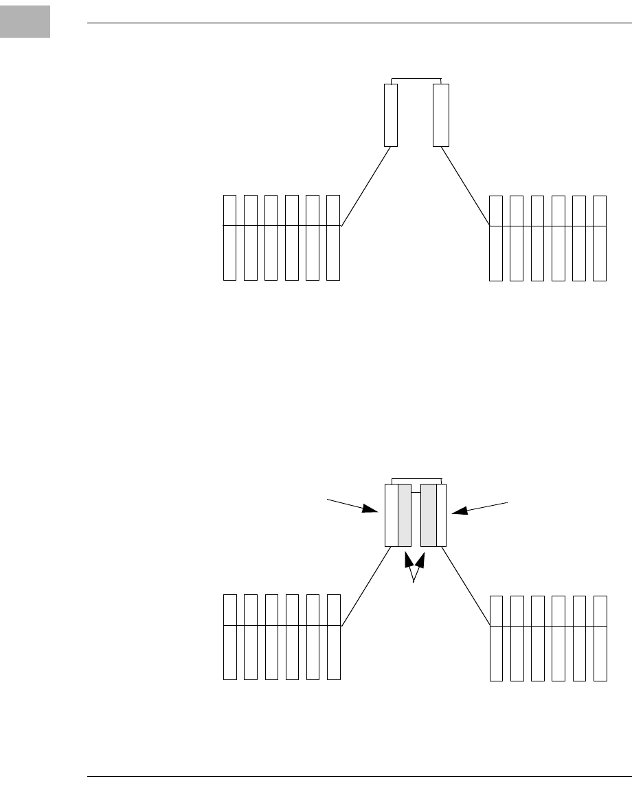
The CPX8216 is a 16-slot, high-availability CompactPCI system with two
separate 6-slot CompactPCI I/O domains and the capability to contain
redundant CPU modules and redundant Hot-Swap Controller (HSC)
modules. It is also possible to configure the system as a simplex, high I/O
system containing a single CPU-HSC pair. Even as a simplex system, the
CPX8216 still provides improved availability through redundant power
supplies and the control/monitoring capabilities of the HSC, as described
in The Hot Swap Controller/Bridge (HSC) Module on page 1-5.
CPX8216
The CPX8216 standard system consists of two 8-slot subsystems, or
domains, each with two slots for the host processor and six slots for
nonhost CompactPCI boards. The HSC board mounts in the rear of the
chassis, behind the secondary CPU slot. Figure 1-2 on page 1-3 provides a
diagram of this configuration.
Bus A Bus B
Alarm Controls
Power Supply/Fan Trays
Drive
Bays
Domain A Domain B Domain A/B
CPX8216
http://www.motorola.com/computer/literature 1-3
1
Figure 1-2. CPX8216 Standard System Layout
Each of the two independent I/O domains has its own system processor
slot. Each system processor has direct access to its local bus through an
onboard PCI-to-PCI (P2P) bridge. Each domain is also capable of
supporting a Hot Swap Controller (HSC) module that contains its own P2P
bridge. Thus, in a fully redundant configuration, there are two bridges that
have access to each of the I/O buses—one associated with the CPU and one
with the HSC. Only one of the bridges may be active at a time, however.
2450 9812
1234567 9 111213141516
Segment A
I/O Slots Segment B
I/O Slots
Front Card Locations
Rear Card Locations
Segment B
HSC Segment A
HSC
Segment B
Transition Slots
Segment B
CPU Transition Module
Compact PCI
Segment A Compact PCI Bus
Segment B
Segment A
CPU Transition Module
Segment B
Transition Slots
1-4 Computer Group Literature Center Web Site
System Architecture
1
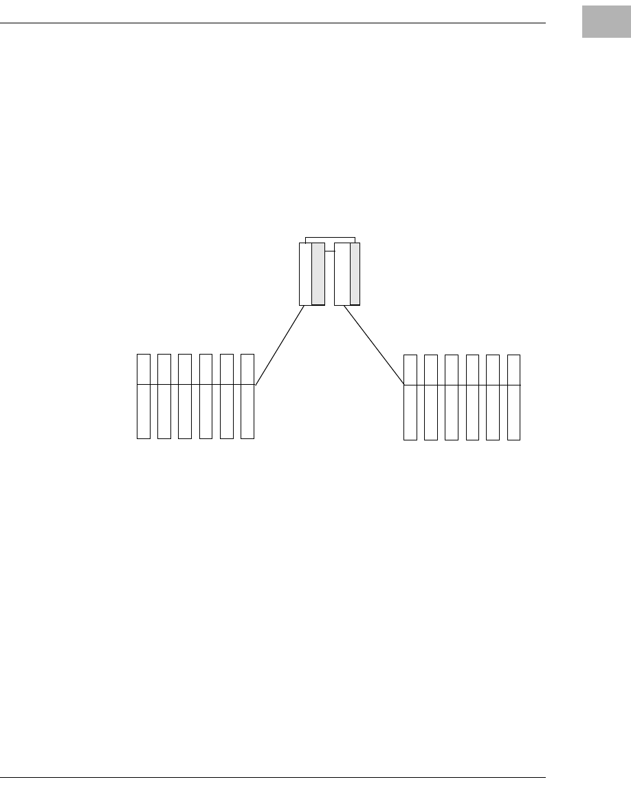
CPX8216T (H.110)
The CPX8216T H.110 system consists of two 8-slot subsystems, or
domains, each with one slot for the host processor, one slot for the front-
loaded HSC, and six slots for nonhost CompactPCI boards. Figure 1-3 on
page 1-4 provides a diagram of this configuration.
Figure 1-3. CPX8216T H.110 System Layout
Bus Access and Control
In the fully redundant configuration, the CPU in the left system slot, CPU
A, is associated with the HSC in the right HSC slot, HSC A (note that HSC
A actually sits on the Domain B bus). There is a local connection between
each CPU-HSC pair that allows the CPU in one domain to control the other
domain through its HSC. This architecture is illustrated in the following
figure.
1234567 9 111213141516
Segment A
I/O Slots Segment B
I/O Slots
Front Card Locations
Rear Card Locations
Segment B
HSC Segment A
HSC
Segment B
Transition Slots
Segment B
CPU Transition Module
Compact PCI
Segment A Compact PCI Bus
Segment B
Segment A
CPU Transition Module
Segment B
Transition Slots
810
CPU
ACPU
B
The Hot Swap Controller/Bridge (HSC) Module
http://www.motorola.com/computer/literature 1-5
1
Figure 1-4. CPX8216 I/O Bus Connectivity
In addition to providing bridges to the remote I/O buses, the HSC provides
the services necessary to hot swap CPU boards and nonhost processor
boards and also controls the system alarm panel, fans, and power supplies.
The Hot Swap Controller/Bridge (HSC) Module
The HSC module connects to the CPU module through a local PCI bus, as
illustrated in Figure 1-2 and Figure 1-3. The HSC module contains a PCI-
to-PCI bridge and also contains a Hot Swap Controller.
The functionality provided by the HSC is at the heart of the High
Availability CPX8216 System. Its primary functions include:
❏Providing a bridge between the two eight-slot CompactPCI buses
so that they can be managed by a single CPU module
❏Maintaining a Control Status Register which contains information
on the status of each system module
I/O
S
L
O
T
I/O
S
L
O
T
I/O
S
L
O
T
I/O
S
L
O
T
I/O
S
L
O
T
I/O
S
L
O
T
I/O
S
L
O
T
I/O
S
L
O
T
I/O
S
L
O
T
I/O
S
L
O
T
I/O
S
L
O
T
I/O
S
L
O
T
C
P
U
C
P
U
H
S
C
H
S
C
Special Backplane
Primary CompactPCI
Buses
I/O Domain A I/O Domain B
ABA
B
PCI Interconnects

1-6 Computer Group Literature Center Web Site
System Architecture
1
❏Controlling power and resets to each system module through
radial connections
❏Monitoring and controlling CPU boards, nonhost boards, and
peripherals, including power and fan sleds, board and system
LEDs, and alarms
Hot Swap Controller
Each of the nonhost slots in the system can be controlled from either HSC.
When an HSC has control over a domain it has control over the nonhost
boards in that domain. Each host processor/bridge pair is controlled as a
single item by the other processor/bridge pair. The bridge and the host
processor are linked together so that both must be present for power to be
applied. A host processor cannot be operated without its HSC.
With the CPX8216 architecture it is important that the system initializes to
a state that allows the host processors and HSCs to be in control of the
system. The default conditions are:
❏System processors and bridges are powered up (if present)
❏System processors and bridges are disconnected from their busses
❏HSCs are not in control of either domain
❏Nonhost boards are powered off
❏Peripheral bays are powered up (if present)
❏Fans and power supplies are powered on
Note System components such as fans and power supplies may be
controlled by either HSC but not both. Default control belongs to
Domain A and whichever HSC has control of Domain A has
control of the system functions.
If Domain A is not controlled, nonhost boards are powered-off
and all LED updates to the display panel and power supplies are
suspended. Also, monitoring of alarm inputs from the display
panel and power supplies are inhibited.

System Processor Configurations
http://www.motorola.com/computer/literature 1-7
1
Subsequent to the default, the system software must determine the
configuration of the system and then proceed to change it.
System Processor Configurations
The CPX8216 is a flexible system that allows for multiple configurations
of processor control, I/O redundancy, and peripheral configurations. The
following sections briefly touch on possible configurations.
As noted above, there are three possible processor/control configurations:
❏A simplex system containing a single CPU-HSC pair controlling
both I/O domains
❏An active/passive configuration similar to the simplex
configuration, but providing a warm backup for both the CPU and
the HSC
❏An active/active or load-sharing configuration in which each CPU
runs a single domain while also serving as a backup to the other
CPU.
Note H.110 traffic and HA Linux do not support a load-
sharing configuration.
The following sections give a general description of these configurations.
The Simplex Configuration
Because of the flexible nature of the CPX8216, it is possible to configure
it with different levels of redundancy and availability. For applications
which do not require the benefits of full high availability, it is possible to
configure the CPX8216 as a simplex, 16-slot system. This configuration
provides the benefits of redundant power supplies and the system
monitoring capabilities of the fully redundant configuration.
1-8 Computer Group Literature Center Web Site
System Architecture
1
The simplex configuration is illustrated in the following figure.
The Active/Passive Configuration
In the active/passive configuration, one CPU manages all twelve I/O slots,
much like in the simplex configuration. In addition, the second CPU serves
as a warm standby, ready to run the system in the event of a failure on the
active system.
The active/passive configuration is illustrated in the following figure.
I/O
S
L
O
T
I/O
S
L
O
T
I/O
S
L
O
T
I/O
S
L
O
T
I/O
S
L
O
T
I/O
S
L
O
T
I/O
S
L
O
T
I/O
S
L
O
T
I/O
S
L
O
T
I/O
S
L
O
T
I/O
S
L
O
T
I/O
S
L
O
T
C
P
U
H
S
C
I/O Domain A I/O Domain B
AA
I/O
S
L
O
T
I/O
S
L
O
T
I/O
S
L
O
T
I/O
S
L
O
T
I/O
S
L
O
T
I/O
S
L
O
T
I/O
S
L
O
T
I/O
S
L
O
T
I/O
S
L
O
T
I/O
S
L
O
T
I/O
S
L
O
T
I/O
S
L
O
T
C
P
U
C
P
U
H
S
C
H
S
C
I/O Domain A I/O Domain B
ABA
B
Active CPU Active HSC
Passive
CPU/HSC
The Active/Active or Load-Sharing Configuration
http://www.motorola.com/computer/literature 1-9
1
The Active/Active or Load-Sharing Configuration
In the load sharing configuration, each CPU manages six of the twelve I/O
slots, much like a dual 8-slot system with the added benefit of one CPU
being able to control all twelve I/O slots if the other CPU fails. It is
important in a load-sharing configuration to note that the total critical
activity does not exceed the capabilities of a single CPU, because either
one of the CPUs must be ready to take over the load carried by the other.
The active/active configuration is illustrated in the following figure.
Note H.110 traffic and HA Linux do not support a load-sharing
configuration.
I/O
S
L
O
T
I/O
S
L
O
T
I/O
S
L
O
T
I/O
S
L
O
T
I/O
S
L
O
T
I/O
S
L
O
T
I/O
S
L
O
T
I/O
S
L
O
T
I/O
S
L
O
T
I/O
S
L
O
T
I/O
S
L
O
T
I/O
S
L
O
T
C
P
U
C
P
U
H
S
C
H
S
C
I/O Domain A I/O Domain B
ABAB

1-10 Computer Group Literature Center Web Site
System Architecture
1
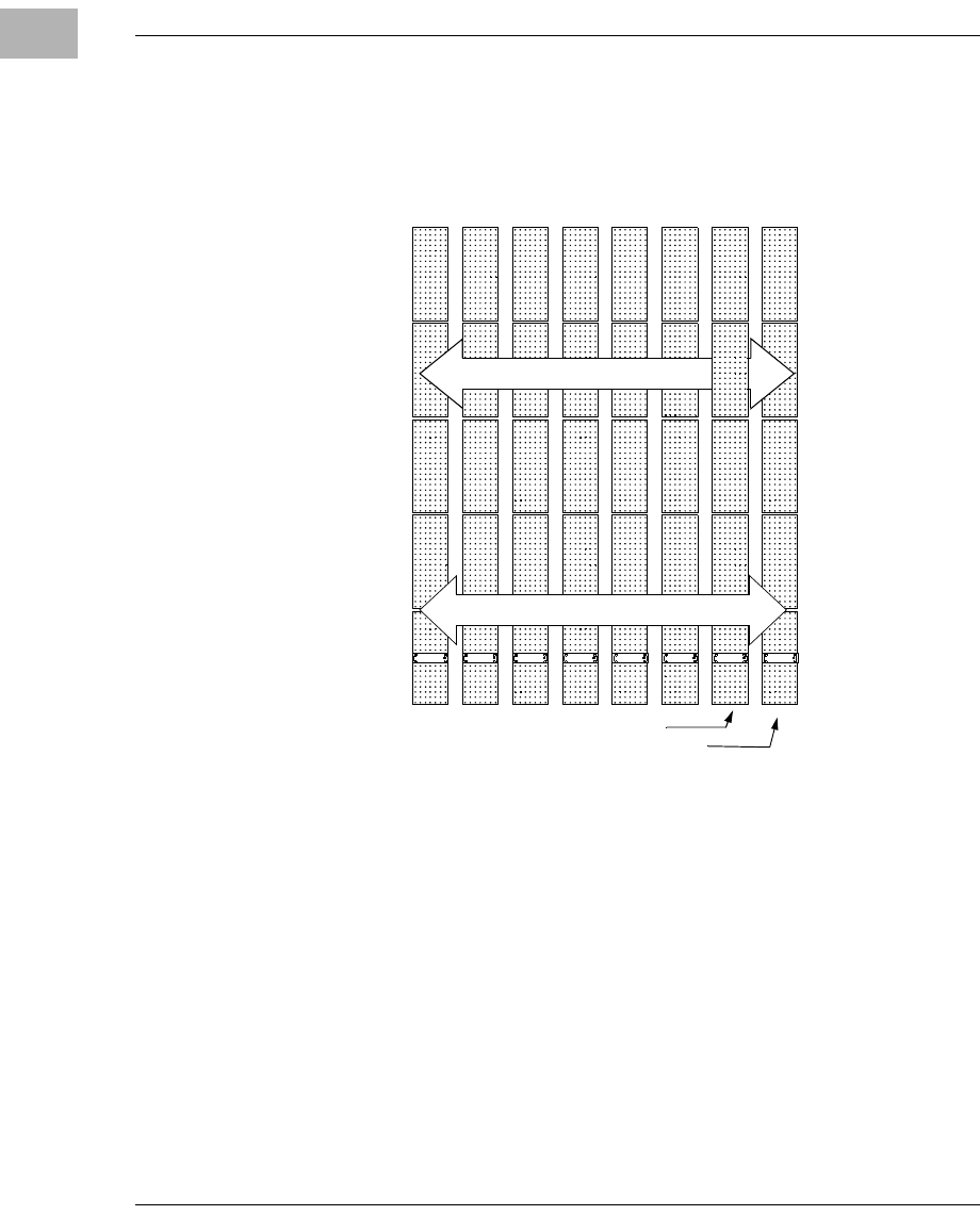
I/O Configurations
The CPX8216 contains two independent 8-slot CompactPCI buses. One
slot in each bus is dedicated to a system processor, and another is needed
for the HSC. This leaves six slots on each bus to support I/O devices or
nonsystem processors.
One possible configuration is to use the CPX8216 as a high I/O
CompactPCI system with redundant CPUs. With this configuration, it is
possible to run twelve independent I/O modules within a CPX8216
system. Applications requiring dense processing power could use all
twelve I/O slots to support nonsystem processors.
Such a system would be protected against a CPU or HSC fault, but it would
be vulnerable to data losses if any of the I/O modules or nonsystem
processor modules were to fail. In systems handling critical data, it is
possible to implement a 2N or an N+1 I/O redundancy strategy that allows
the level of service to be continued in the event that a module fails.
In the case of a 2N-redundant system, each I/O module or nonsystem
processor module is matched with an identical module on the other bus.
The paired modules can be configured in an active/passive arrangement or
a load-sharing arrangement in which each carries half of the load of a
single module. In an N+1 arrangement, multiple modules are backed up by
a single spare. For example, a single passive nonsystem processor module
can be used to back up five others.
Peripherals
Power/Fan Modules
The CPX8216 system requires a minimum of two power/fan sled modules
and a fan-only sled module to provide adequate power and cooling for a
fully loaded, nonredundant system. The system can contain a third power
supply/fan sled as part of an N+1 strategy, meaning that the system can
continue providing service if one of the modules fails. These modules are
hot swappable and available for DC and AC environments.

Drive Modules
http://www.motorola.com/computer/literature 1-11
1
The fans run at either high speed (default) or temperature controlled, which
can be changed using the operating system software via the API.
Drive Modules
The CPX8216 contains four hot-swappable peripheral bays, all of which
support both SCSI and EIDE protocols.
!
Caution
Caution The hot swapping of hard drives is supported when your system is
configured with the appropriate software support for hot swap and when
the drives are in a hot-swap drive carrier.
SCSI devices can be configured to be fully hot-swappable, and data can be
hot switched between two independent SCSI controllers. EIDE devices are
assigned to a single EIDE controller. They can be warm swapped, meaning
that a failed device can be replaced once the controller has been powered
off.
The rear of the CPX8216 chassis may be configured with either single or
double, fixed, floppy drives. Floppy drives are not hot-swappable.
For more information on installing both hot-swappable and non-hot-
swappable drives, refer to the Drive Removal and Installation chapter of
the CPX8216 and CPX8216T CompactPCI System Installation and Use
manual.
1-12 Computer Group Literature Center Web Site
System Architecture
1
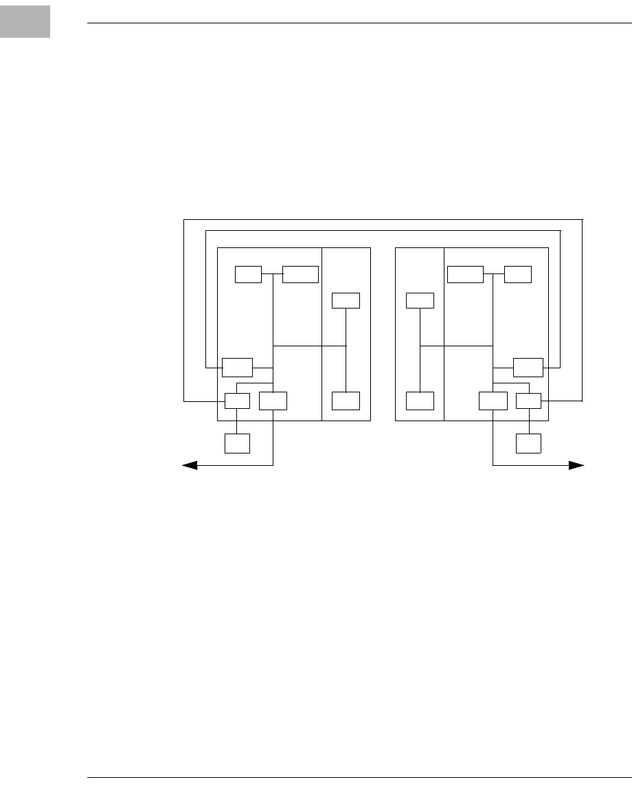
CPU Complex Architecture
The CPU complex in the CPX8216 contains two CPU modules and their
corresponding Hot Swap Controller (HSC) modules. The figure below
illustrates the architecture, including elements on the boards as well as
local connections between the CPU modules and the PCI-to-PCI (P2P)
connections to the local CompactPCI buses.
The CPU Module
In addition to the processor, RAM, etc., each CPU module contains one:
❏Up to two Ethernet controllers
❏Up to two serial communications links
❏P2P bridge to the local CompactPCI bus
❏Local PCI Bus connection to the HSC
HSC
P2P
RAM
Enet
ISA
IDE
Proc
P2P
HSC
P2P
RAM
Enet
ISA
IDE
Proc
P2P
Local Connections between CPU Modules
CompactPCI BusCompactPCI Bus
Link
Serial
Link
Serial

Switching Service to the Passive CPU
http://www.motorola.com/computer/literature 1-13
1
Switching Service to the Passive CPU
The switchover from one CPU to another is initiated by the passive CPU
when there is an indication that there is something wrong with the active
CPU--such as a failed heartbeat protocol. The passive side notifies the
active side that it is about to begin a switchover process. If the active side
agrees to the switchover, then the two sides coordinate the hand-off and no
bus signals, clocks, or devices should be corrupted. If the active system
fails to cooperate with the takeover attempt, then we must assume that bus
signals, clocks, and devices attached to the bus may be corrupted.
In a more extreme takeover, it is possible for the passive CPU to power-on
reset the active CPU and to take control that way.
Chassis ID for CPX8216T
A unique 5-bit chassis ID can be assigned for each CPX8216T system.
Hex values are on the rotary switches located on the HSC boards. A jumper
can be added to J14 to double the number of unique identifiers. This
feature should be used if more than 15 chassis are deployed in one location.
The HSC boards are shipped with no jumper as the default. For guidelines
on setting the chassis ID on your CPX8216T system, refer to the CPX8000
Series CPX8216 and CPX8216T CompactPCI System Installation and Use
manual.
Alarms and LEDs
In order to provide a uniform appearance, without depending on individual
board manufacturers, the CPX8216 contains a separate alarm display
panel, which runs across the top of the chassis. In addition to In
Service/Out of Service LED indicators for all sixteen slots, the alarm
display panel contains LEDs for system status (System in
Service/Component out of Service/System out of Service) and for the three
standard Telco levels (Critical/Major/Minor). The three Telco alarms are
also signalled through a dry contact relay.
1-14 Computer Group Literature Center Web Site
System Architecture
1
H.110 Telephony Bus
The CPX8216T supports an H.110 Computer Telephony Bus. The H.110
bus uses P4/J4 as defined in the PICMG specification for CompactPCI.
Figure 1-5. The CPX8216T H.110 Bus
Board Insertion and Extraction Features
The PICMG specification details software and hardware features, in order
to support hot swapping of I/O boards. Hardware features include:
❏Staged pins that control voltages when inserting or extracting
boards
❏BD_SEL#, HEALTHY#, and ENUM# signals
❏Hot swap control status register
2557 9906
P5
P4
P3
P2
P1
H. 110 Bus
CompactPCI Bus
System Slot
HSC Slot

Staged Pins
http://www.motorola.com/computer/literature 1-15
1
Staged Pins
The PICMG CompactPCI hot swap specification provides for three
separate pin lengths in order to control the insertion and extraction
voltages and to notify the system when boards are inserted or extracted.
The longest pins, which include VCC pins and GND pins, are the first to
mate during the insertion process and the last to break contact during
extraction. These pins are used to supply power to pre-charge the PCI
interface signals to a neutral state before they contact the bus. This pre-
charging serves to minimize the capacitive effects of the board as it makes
or breaks contact with the bus.
The medium-length pins carry PCI and other signal traffic.
The shortest pins are used to assert signals, including BD_SEL#. During
insertion, the BD_SEL# signal enables the board to attach to the local PCI
bus. On extraction, it causes the board to logically and electrically
disconnect from the PCI bus before the bus pins physically break contact
with the bus.
BD_SEL#
BD_SEL# is asserted by one of the pins that mate last on insertion and
break first on extraction. On insertion, the signal tells the board to connect
to the PCI bus. On extraction this pin breaks first, causing the board to
logically and electrically disconnect from the PCI bus before the PCI bus
pins physically break contact with the bus.
ENUM#
An ENUM interrupt is generated when a board is hot inserted into the
CPX8216 chassis, or when an operator trips the board microswitch by
raising its ejector handles. The signal informs the active CPU that the
status of a board has changed. The CPU then identifies the board by polling
the INSert and EXTract bits in all of the boards’ Control Status Registers.
1-16 Computer Group Literature Center Web Site
System Architecture
1
Hot Swap Control Status Register (CSR)
The CPX8216 supports hot swap CompactPCI cards with the standard
control status register defined by the PICMG Hot Swap Specification. The
register is visible in PCI configuration space and provides hot swap control
and status bits: INS and EXT. The INS signal is set when ENUM# is
asserted by a board being inserted into the system. The EXT signal is
asserted when ENUM# is asserted by an operator triggering the
microswitch in the board handles. The host also uses these bits to
acknowledge and de-assert ENUM#.
The Hot Swap Process
PICMG divided the complete hot swap process into physical, hardware
and software connection processes. These processes are formally broken
down further into a group of transitional states, which are illustrated in the
following figure.
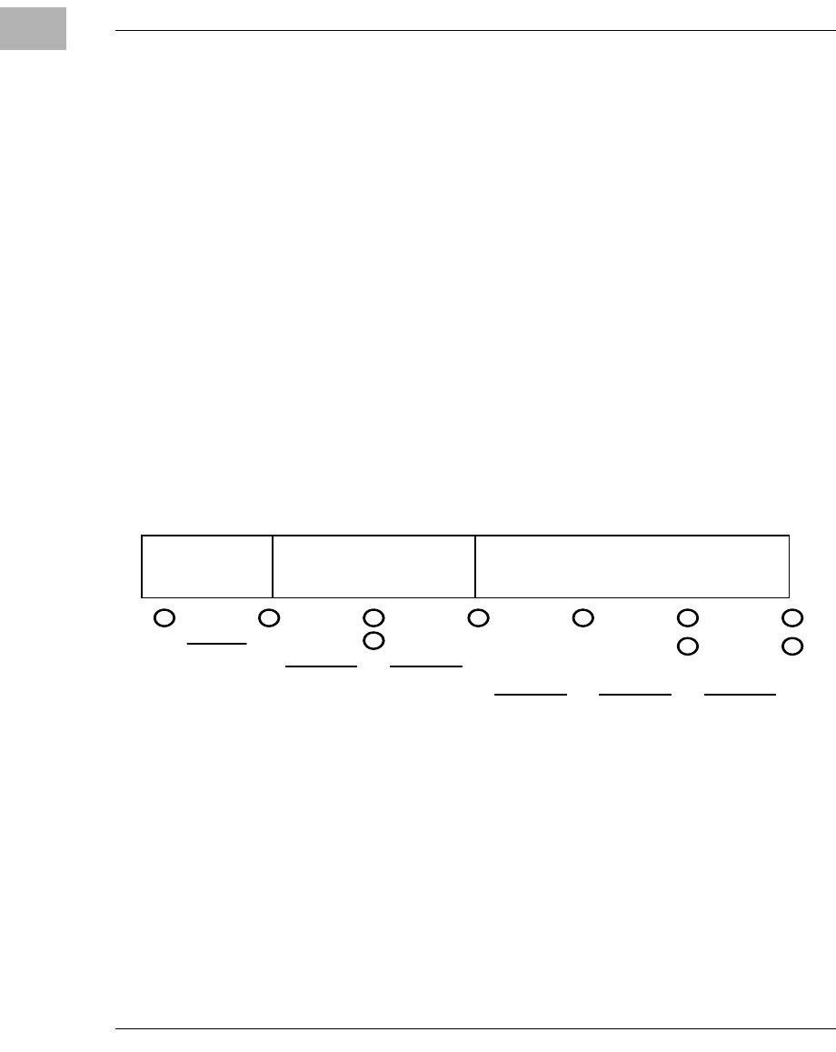
When inserting a board, it goes through all states from P0 to S3.
Conversely, a board transitions from S3 to P0 before being extracted.
During normal operation, no states are skipped. Extracting a board in a
software connection state other than S0 is likely to disrupt software enough
to crash the system, but the CompactPCI bus, from a purely electrical point
of view, will not be disrupted enough to cause logic levels to be violated.
Certain states are overlapping. For example, when the board is fully seated
(completed P1), but has not yet started the hardware connection process
P0 P1
H0 H1
S1
H2
S0 S2 S3
PHYSICAL
CONNECTION
STATES
HARDWARE
CONNECTION STATES SOFTWARE
CONNECTION
STATES
H1F
S2Q S3Q

Physical Connection Process
http://www.motorola.com/computer/literature 1-17
1
(H0), it said to be in the P1/H0 state. Similarly, one can speak of a board
being in the H2/S0 state.
Physical Connection Process
The physical connection process is the basic process of putting a board into
a live system, or physically removing the board. The process includes two
states:
❏P0 - The board is physically separate from the system
❏P1 - The board is fully seated, but not powered, and not active on
the PCI bus. All pins are connected.
Hardware Connection Process
The hardware connection process involves the electrical connection or
disconnection of the board. This process includes three states:
❏H0 - The board is not active on the PCI bus. This state is equivalent
to P1 above.
❏H1 - The board has powered up and is sufficiently initialized to
connect to the PCI bus.
❏H2 - The board is powered, and enabled for access by a PCI bus
transaction (normally by the host) in PCI configuration space only.
The board configuration space is not yet initialized.
When a newly inserted board has completed H2, the board is operable
from a hardware perspective. It has run its power up diagnostics, initialized
itself, loaded EEPROM data, etc. The blue LED is off in the H2 state,
indicating that the board should not be pulled out.

1-18 Computer Group Literature Center Web Site
System Architecture
1
Software Connection Process
The software connection process includes the tasks needed to configure
and load software. This process contains four states:
❏S0 - The Software Connection Process has not been initiated. The
board’s configuration space registers are accessible but not yet
initialized.
❏S1 - The board is configured by the system. The system has
initialized the board’s PCI configuration space registers with I/O
space, memory space, interrupts and PCI bus numbers. The board
is ready to be accessed by a device driver, but no drivers are loaded
at this time.
❏S2 - The necessary supporting software (drivers, etc.) have been
loaded. The board is ready for use by the OS and/or the
application, but no operations involving the board are active or
pending.
❏S3 - The board is active. Software operations are either active or
pending.
Software Disconnection Process
The software disconnection process defines two additional states which
are used when quiescing activity on a board in preparation for extraction:
❏S3Q - The software is completing current operations, but is not
allowed to start new ones. When current operations are completed,
the board transitions to S2.
❏S2Q - The board is quiesced. This is the same state as S2, except
that no new operations are allowed to be initiated.
The Software Disconnection Process proceeds as S3, S3Q, S2Q, S1, and
finally S0.

Typical Insertion and Extraction Processes
http://www.motorola.com/computer/literature 1-19
1
Typical Insertion and Extraction Processes
Many of the steps in the insertion and extraction processes are automated
by software. After the operator installs a board, it automatically advances
to P1. The hardware connection process proceeds automatically and
asserts the ENUM# signal to initiate the software connection process. The
host responds to the bussed ENUM# signal by reading the Hot Swap
Control Status Register of each board to find out which one is signaling an
insertion or extraction (INS or EXT bit asserted). Upon detecting an
insertion, the Host responds by adding software drivers to support the
newly inserted board.
Extraction is initiated when the operator opens the board ejector handle,
which activates a mechanical switch to assert ENUM#. The hot plug
system driver senses ENUM# and notifies software that board activity
must be quiesced and that software device drivers should be unloaded. The
application that is using the board is informed that the resource is no longer
available. When the board is ready for extraction, software informs the
operator by illuminating the blue LED. After extraction, all system
resources previously assigned to that board are made available for other
uses.
Device Drivers
In order to take full advantage of the high availability functions of the
CPX8216, and to support hot swap, board device drivers need to be
enhanced. Drivers need to cease all activity when the device is about to be
hot swapped, and they need to support initialization of the device without
support from the device firmware or BIOS.
Further, high availability device drivers need to be able to enter a standby
mode while bus control is being passed from one CPU to another. They
also provide diagnostic interfaces for run time fault detection and for pre-
initialization testing of newly inserted boards.
2-1
2
2CPU Modules
Overview
This chapter provides reference information for the CompactPCI system
controller/host CPU modules supported in the CPX8216 system.
The correct jumper setting and pin-out information is provided for each
module.
Note The CPX750HA is sometimes identified as an MCP750HA in
some chassis and firmware documentation, for packaging and
ordering purposes, but both numbers apply to the same board.
Your system may not contain all boards listed in this chapter, or
it may contain third-party boards that are not listed in this
chapter. For information about third-party boards, refer to the
board manufacturer’s documentation.
This chapter contains information for the following CompactPCI boards:
CPX750HA
The CPX750HA is a single-slot, single-board computer equipped with a
PowerPC™ 750 Series microprocessor. The processor implements a
backside cache controller and the board comes with 1MB of cache
memory.
Table 2-1. CompactPCI Boards
Part No. Description Slots
Occupied Page
CPX750HA PowerPC Hot Swappable CPU 1 2-1
CPV5350 Intel Hot Swappable CPU 1 2-16

2-2 Computer Group Literature Center Web Site
CPU Modules
2The CPX750HA offers many standard features desirable in a CompactPCI
computer system, such as:
❏PCI Bridge and Interrupt Controller
❏ECC Memory Controller chipset
❏5MB to 9MB of linear FLASH memory
❏IDE CompactFlash memory
❏16MB to 256MB of ECC-protected DRAM
❏Interface to a CompactPCI bus
❏Several I/O peripherals
The I/O peripheral interfaces present on the onboard PCI bus include:
❏One 10/100-BASE-T Ethernet interface
❏One USB host controller
❏One SA master/slave interface
❏One Fast EIDE interface
❏One PMC Slot
Functions provided from the ISA bus are two asynchronous and two
synchronous/asynchronous serial ports, keyboard, mouse, a floppy disk
controller, printer port, a real time clock, and NVRAM.
The CPX750HA interfaces to a CompactPCI bus using a DEC 21154 PCI-
to-PCI bridge device. This device provides a 64-bit primary and a 64-bit
secondary interface allowing full 64-bit data access between CompactPCI
bus devices and the host/PCI bridge. This bus is capable of driving seven
CompactPCI slots.
Another key feature of the CPX750HA is the PCI (Peripheral Component
Interconnect) bus. In addition to the onboard local bus peripherals, the PCI
bus supports an industry-standard mezzanine interface, IEEE P1386.1
PMC (PCI Mezzanine Card). PMC modules offer a variety of possibilities
for I/O expansion.
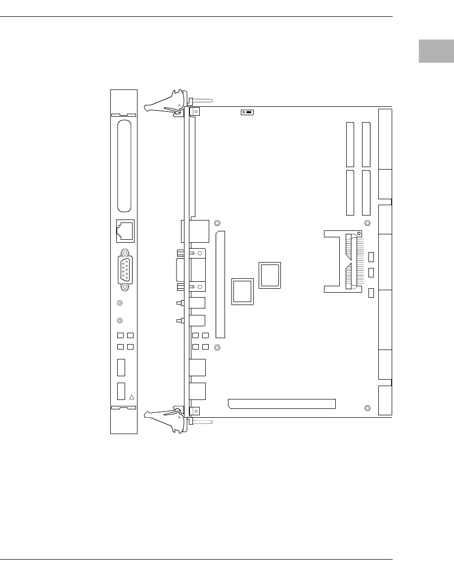
CPX750HA
http://www.motorola.com/computer/literature 2-3
2
The base board supports PMC I/O for the front panel or through backplane
connector J3 to a CPX750HATM transition module.
2213 9804
10/100 BASE T
1
J15
189
1902
1
J10
USB 1
CPI
ABT
BFL
RST
CPU
PCI MEZZANINE CARD
2
DS2
COM 1
4
1
XU2
CPCI
J11
49
50
3
J8
S2S1
1
DS1 DS3
DS4
J17 J18
4
1
15
69
82
71
1
2
J12
49
50
1
2
J13
49
50
1
2
J14
49
50
XU1
USB 0
J6
J5 J4 J3 J2 J1
J9
189
1902
1J19
F1 F2 F3
2-4 Computer Group Literature Center Web Site
CPU Modules
2Connectors and Jumper Settings
The next sections provide pinout information and jumper settings for the
CPX750HA board. Additional pinout assignments can be found in
Chapters 3 through 6.
Backplane Connectors (P5, P4, P3, P2, P1)
Refer to the backplane reference section for the backplane connector pin
assignments.
Front USB Connectors (J17 and J18)
Two USB Series A receptacles are located at the front panel of the
CPX750HA board. The pin assignments for these connectors are as
follows:
10BaseT/100BaseTx Connector (J8)
The 10BaseT/100BaseTx Connector is an RJ45 connector located on the
front panel of the CPX750HA board. The pin assignments for this
connector are as follows:
Table 2-2. USB 0 Connector J18
1UVCC0
2UDATA0N
3UDATA0P
4GND
Table 2-3. USB 1 Connector J17
1UVCC1
2UDATA1N
3UDATA1P
4GND
Connectors and Jumper Settings
http://www.motorola.com/computer/literature 2-5
2
COM1 Connector (J15)
A standard DB9 receptacle is located on the front panel of the CPX750HA
to provide the interface to the COM1 serial port. These COM1 signals are
also routed to J11 on the transition module. A terminal may be connected
to J15 or J11 on the transition module but not both at the same time. The
pin assignments for this connector is as follows:
Table 2-4. 10BaseT/100BaseTx Connector J8
1TD+
2TD-
3RD+
4AC Terminated
5AC Terminated
6RD-
7AC Terminated
8AC Terminated
Table 2-5. COM1 Connector J15
1DCD
2RXD
3TXD
4DTR
5GND
6DSR
7RTS
8CTS
9RI
2-6 Computer Group Literature Center Web Site
CPU Modules
2Debug Connector (J19)
A 190-pin connector (J19 on the CPX750HA base board) provides access
to the processor bus (MPU bus) and some bridge/memory controller
signals. It can be used for debugging purposes. The pin assignments are
listed in the following table.
Table 2-6. Debug Connector (J19)
1PA0 PA1 2
3PA2 PA3 4
5PA4 PA5 6
7PA6 PA7 8
9PA8 PA9 10
11 PA10 PA11 12
13 PA12 PA13 14
15 PA14 PA15 16
17 PA16 PA17 18
19 PA18 GND PA19 20
21 PA20 PA21 22
23 PA22 PA23 24
25 PA24 PA25 26
27 PA26 PA27 28
29 PA28 PA29 30
31 PA30 PA31 32
33 PA_PAR0 PA_PAR1 34
35 PA_PAR2 PA_PAR3 36
37 APE* RSRV* 38
39 PD0 PD1 40
41 PD2 PD3 42
Connectors and Jumper Settings
http://www.motorola.com/computer/literature 2-7
2
43 PD4 PD5 44
45 PD6 PD7 46
47 PD8 PD9 48
49 PD10 PD11 50
51 PD12 PD13 52
53 PD14 PD15 54
55 PD16 PD17 56
57 PD18 +5V PD19 58
59 PA20 PD21 60
61 PD22 PD23 62
63 PD24 PD25 64
65 PD26 PD27 66
67 PD28 PD29 68
69 PD30 PD31 70
71 PD32 PD33 72
73 PD34 PD35 74
75 PD36 PD37 76
77 PD38 PD39 78
79 PD40 PD41 80
81 PD42 PD43 82
83 PD44 PD45 84
85 PD46 PD47 86
87 PD48 PD49 88
89 PA50 PD51 90
91 PD52 PD53 92
93 PD54 PD55 94
Table 2-6. Debug Connector (J19) (continued)

2-8 Computer Group Literature Center Web Site
CPU Modules
2
95 PD56 GND PD57 96
97 PD58 PD59 98
99 PD60 PD61 100
101 PD62 PD63 102
103 PDPAR0 PDPAR1 104
105 PDPAR2 PDPAR3 106
107 PDPAR4 PDPAR5 108
109 PDPAR6 PDPAR7 110
111 No Connection No Connection 112
113 DPE* DBDIS* 114
115 TT0 TSIZ0 116
117 TT1 TSIZ1 118
119 TT2 TSIZ2 120
121 TT3 No Connection 122
123 TT4 No Connection 124
125 CI* No Connection 126
127 WT* No Connection 128
129 GLOBAL* No Connection 130
131 SHARED* DBWO* 132
133 AACK* +3.3V TS* 134
135 ARTY* XATS* 136
137 DRTY* TBST* 138
139 TA* No Connection 140
141 TEA* No Connection 142
143 No Connection DBG* 144
145 No Connection DBB* 146
Table 2-6. Debug Connector (J19) (continued)
Connectors and Jumper Settings
http://www.motorola.com/computer/literature 2-9
2
147 No Connection ABB* 148
149 TCLK_OUT MPUBG-0* 150
151 No Connection MPUBR0* 152
153 MPUBR1* IRQ0* 154
155 MPUBG1* MCHK* 156
157 WDT1TO* SMI* 158
159 WDT2TO* CKSTPI* 160
161 L2BR* CKSTPO* 162
163 L2BG* HALTED (N/C) 164
165 CLAIM* TLBISYNC* 166
167 No Connection TBEN 168
169 No Connection* No Connection 170
171 No Connection* GND No Connection 172
173 No Connection* No Connection 174
175 No Connection NAPRUN 176
177 SRST1* QREQ* 178
179 SRESET* QACK* 180
181 HRESET* CPUTDO 182
183 GND CPUTDI 184
185 CPUCLK1 CPUTCK 186
187 No Connection CPUTMS 188
189 No Connection CPUTRST* 190
Table 2-6. Debug Connector (J19) (continued)
2-10 Computer Group Literature Center Web Site
CPU Modules
2DRAM Mezzanine Connector (J10)
A 190-pin connector (J10 on the CPX750HA base board) supplies the
interface between the memory bus and the RAM300 DRAM mezzanine.
The pin assignments are listed in the following table.
Table 2-7. DRAM Mezzanine Connector (J10)
1A_RAS∗A_CAS∗2
3B_RAS∗B_CAS∗4
5C_RAS∗C_CAS∗6
7D_RAS∗D_CAS∗8
9OEL∗OEU∗10
11 WEL∗WEU∗12
13 ROMACS∗ROMBCS∗14
15 RAMAEN RAMBEN 16
17 RAMCEN EN5VPWR 18
19 RAL0 GND RAL1 20
21 RAL2 RAL3 22
23 RAL4 RAL5 24
25 RAL6 RAL7 26
27 RAL8 RAL9 28
29 RAL10 RAL11 30
31 RAL12 RAU0 32
33 RAU1 RAU2 34
35 RAU3 RAU4 36
37 RAU5 RAU6 38
39 RAU7 RAU8 40
41 RAU9 RAU10 42
43 RAU11 RAU12 44

Connectors and Jumper Settings
http://www.motorola.com/computer/literature 2-11
2
45 RDL0 RDL1 46
47 RDL2 RDL3 48
49 RDL4 RDL5 50
51 RDL6 RDL7 52
53 RDL8 RDL9 54
55 RDL10 RDL11 56
57RDL12+5VRDL1358
59 RDL14 RDL15 60
61 RDL16 RDL17 62
63 RDL18 RDL19 64
65 RDL20 RDL21 66
67 RDL22 RDL23 68
69 RDL24 RDL25 70
71 RDL26 RDL27 72
73 RDL28 RDL29 74
75 RDL30 RDL31 76
77 RDL32 RDL33 78
79 RDL34 RDL35 80
81 RDL36 RDL37 82
83 RDL38 RDL39 84
85 RDL40 RDL41 86
87 RDL42 RDL43 88
89 RDL44 RDL45 90
91 RDL46 RDL47 92
93 RDL48 RDL49 94
95 RDL50 GND RDL51 96
Table 2-7. DRAM Mezzanine Connector (J10) (continued)
2-12 Computer Group Literature Center Web Site
CPU Modules
2
97 RDL52 RDL53 98
99 RDL54 RDL55 100
101 RDL56 RDL57 102
103 RDL58 RDL59 104
105 RDL60 RDL61 106
107 RDL62 RDL63 108
109 CDL0 CDL1 110
111 CDL2 CDL3 112
113 CDL4 CDL5 114
115 CDL6 CDL7 116
117 No Connection No Connection 118
119 RDU0 RDU1 120
121 RDU2 RDU3 122
123 RDU4 RDU5 124
125 RDU6 RDU7 126
127 RDU8 RDU9 128
129 RDU10 RDU11 130
131 RDU12 RDU13 132
133 RDU14 +3.3V RDU15 134
135 RDU16 RDU17 136
137 RDU18 RDU19 138
139 RDU20 RDU21 140
141 RDU22 RDU23 142
143 RDU24 RDU25 144
145 RDU26 RDU27 146
147 RDU28 RDU29 148
Table 2-7. DRAM Mezzanine Connector (J10) (continued)
Connectors and Jumper Settings
http://www.motorola.com/computer/literature 2-13
2
149 RDU30 RDU31 150
151 RDU32 RDU33 152
153 RDU34 RDU35 154
155 RDU36 RDU37 156
157 RDU38 RDU39 158
159 RDU40 RDU41 160
161 RDU42 RDU43 162
163 RDU44 RDU45 164
165 RDU46 RDU47 166
167 RDU48 RDU49 168
169 RDU50 RDU51 170
171 RDU52 GND RDU53 172
173 RDU54 RDU55 174
175 RDU56 RDU57 176
177 RDU58 RDU59 178
179 RDU60 RDU61 180
181 RDU62 RDU63 182
183 CDU0 CDU1 184
185 CDU2 CDU3 186
187 CDU4 CDU5 188
189 CDU6 CDU7 190
Table 2-7. DRAM Mezzanine Connector (J10) (continued)
2-14 Computer Group Literature Center Web Site
CPU Modules
2EIDE Compact FLASH Connector (J9)
A 50-pin Compact FLASH card header connector provides the EIDE
interface to the Compact FLASH Memory Card. The pin assignments for
this connector are as follows:
Table 2-8. EIDE Compact FLASH Connector J9
1 GND DATA3 2
3 DATA4 DATA5 4
5 DATA6 DATA7 6
7 DCS1A_L GND 8
9 GND GND 10
11 GND GND 12
13 +5V GND 14
15 GND GND 16
17 GND DA2 18
19 DA1 DA0 20
21 DATA0 DATA1 22
23 DATA2 NO CONNECT 24
25 CD2_L CD1_L 26
27 DATA11 DATA12 28
29 DATA13 DATA14 30
31 DATA15 DCS3A_L 32
33 NO CONNECT DIORA_L 34
35 DIOWA_L NO CONNECT 36
37 INTRQA +5V 38
39 MASTER/SLAVE NO CONNECT 40
41 RST_L DIORDYA 42
43 NO CONNECT NO CONNECT 44
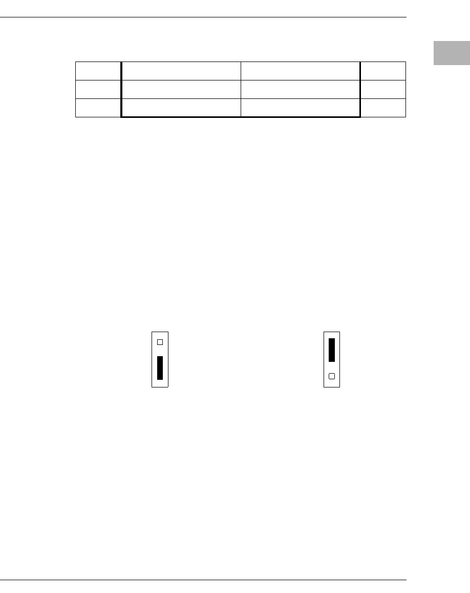
Connectors and Jumper Settings
http://www.motorola.com/computer/literature 2-15
2
Flash Bank Selection (J6)
The CPX750HA base board has provision for 1MB of 16-bit flash
memory. The RAM300 memory mezzanine accommodates 4MB or 8MB
of additional 64-bit flash memory.
The flash memory is organized in either one or two banks, each bank either
16- or 64-bits wide. Bank B contains the onboard debugger, PPCBug.
To enable flash bank A (4MB or 8MB of firmware resident on soldered-in
devices on the RAM300 mezzanine), place a jumper across header J6 pins
1 and 2. To enable flash bank B (1MB of firmware located in sockets on
the base board), place a jumper across header J6 pins 2 and 3.
45 NO CONNECT NO CONNECT 46
47 DATA8 DATA9 48
49 DATA10 GND 50
Table 2-8. EIDE Compact FLASH Connector J9
3
2
1
3
2
1
Flash Bank A Enabled (4MB/8MB, Soldered) Flash Bank B Enabled (1MB, Sockets)
J6J6
(Factory Configuration)

2-16 Computer Group Literature Center Web Site
CPU Modules
2CPV5350
The CPV5350 Single Board Computer (SBC) is a hot swap, CompactPCI
(Compact Peripheral Communication Interface) compliant computer with
high availability platform support. It is powered by a PICMG (PCI
Industrial Computer Manufacturers Group) compatible Pentium® II
Deschutes Mobile Module. The CPV5350’s 6U CompactPCI standard
form factor (160mm x 233mm x 61mm), 4HP (.8 inch) is designed for
installation into PICMG CompactPCI-compliant backplanes.
The CPV5350 provides:
❏Standard PC I/O
❏USB
❏PCI EIDE
❏3D AGP graphics
❏Dual fast Ethernet controllers
❏Optional onboard CompactFlash™ connector
The CPV5350’s front panel has connectors for:
❏Keyboard/mouse
❏Video
❏Two serial ports (COM1 and COM2)
❏Two Ethernet ports
❏Two USB ports
❏LED Indicator lights for watchdog alarm, speaker status, hard disk
drive activity, and power.
Refer to the following illustration for front panel connectors and LEDs on
the CPV5350.
2-18 Computer Group Literature Center Web Site
CPU Modules
2Connectors
The next table lists the connectors available to support devices on the
CPV5350. Figure 2-1 on page 2-19 shows the location of the connectors
described in the table.
Table 2-9. CPV5350 Front Panel Connectors, Board
Headers and Components
Connector Description
J1 Backplane connector
J2 Backplane connector
J3 Backplane connector
J4 Backplane connector
J5 Backplane connector
J6 Ethernet 2
J9 EIDE
J10 Reserved (in-circuit programming)
J12 Reserved (in-circuit emulator)
J13 Ethernet 1
J14 USB port 1
J16 Reset (connected to push-button on the front panel)
J21 Flash ROM
J23 Video connector
J24 COM1 (Serial Port 1)
J25 COM2 (Serial Port 2)
J50 Keyboard/Mouse
Transition Module
http://www.motorola.com/computer/literature 2-19
2
Figure 2-1. CPV5350 Component Side View
Transition Module
The CPV5350TM80 transition module provides backplane I/O through the
J3 and J5 connectors on the CPV5350 controller module.
When the identical function is available through the CPV5350’s front
panel and the rear transition module, you can use either the front or the
rear, not both.
J13 J6
J51
J12
21
12
J20
2
1
J17
1
8
J21
T1 T2
U55
U62
BT1
U25 U26
U50
U38
U11
J23
CRI
CR2 CR4
CR3
J14 J50
U34 U35
U30 U31
J24 J25
2475 99012475 9901
J1
J2
J3
J4
J5
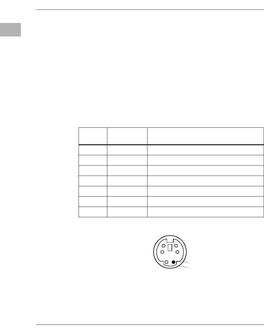
2-20 Computer Group Literature Center Web Site
CPU Modules
2DRAM Memory Configuration
The CPV5350 has one 168-pin DIMM site for memory expansion. The
DIMM sites accept industry standard PC100-compliant DIMM modules
(8, 16, 32, 64, 128, or 256MB) with or without ECC. You can use either
registered or unbuffered memory modules.
Keyboard/Mouse PS2 Connector
The keyboard/mouse connector (J50) uses a 6-pin, female PS/2 connector.
Figure 2-2. Keyboard/Mouse Connector Diagram
Table 2-10. Keyboard/Mouse P/S2 Connector Pin
Assignments (J50)
Pin
Number Signal
Mnemonic Signal Description
1 KBDDAT Keyboard Data
2 AUXDAT Auxiliary Data
3 GND Ground
4 KBDVCC Keyboard Power (current limited to .75 Amp)
5 KBDCLK Keyboard Clock
6 AUXCLK Auxiliary Clock
7 CGND Common Ground
2489 9902
6
4
2
5
3
1
7
Ethernet Connectors
http://www.motorola.com/computer/literature 2-21
2
Ethernet Connectors
Ethernet 1 (J13) and Ethernet 2 (J6) use standard RJ-45 connectors.
Universal Serial Bus (USB) Connector
USB Port 1 and Port 2 (J14) use a 2 x 4 pin USB connector.
Table 2-11. Ethernet Connector Pin Assignments (J13 and
J6)
Pin
Number Signal Mnemonic Signal Description
1 TX+ Differential transmit lines
2 TX- Differential transmit lines
3 RX+ Differential receive lines
4-- --
5-- --
6 RX- Differential receive lines
7-- --
8-- --
Table 2-12. USB Connector Pin Assignments (J14)
Pin
Number Signal Mnemonic Signal Description
1 +5V Current limited USB power
2 DATA+ USB serial communication differential
3 DATA- USB serial communication differential
4 GND USB port common
2-22 Computer Group Literature Center Web Site
CPU Modules
2Serial Port Connectors
COM 1 (Serial Port 1) (J24) and COM 2 (Serial Port 2) (J25) use 2 x 9-pin
D-sub connectors.
Video Connector
The video connector (J23) uses a 15-pin high density D-sub connector.
Table 2-13. Serial Port Connector Pin Assignments (J24
and J25)
Pin
Number Signal
Mnemonic Signal Description
1 DCD- data set has detected the data carrier
2 RX Receives serial data input from communication
link
3 TX Sends serial output to communication link
4 DTR- data set is ready to establish a communication link
5 GND Ground
6 DSR- data set is ready to establish a communication link
7 RTS- indicates to data set that UART is ready to
exchange data
8 CTS- data set is ready to exchange data
9 RI- modem has received a telephone ringing signal
Table 2-14. Video Connector Pin Assignments (J23)
Pin
Number Signal Mnemonic Signal Description
1 RED Red signal
2 GREEN Green signal
3 BLUE Blue signal
Video Connector
http://www.motorola.com/computer/literature 2-23
2
4 NC Not connected
5 DACVSS Video return
6 DACVSS Video return
7 DACVSS Video return
8 DACVSS Video return
9 NC Not connected
10 DACVSS Video return
11 NC Not connected
12 DDCDAT Display data channel data signal for
DDC2 support
13 HSYNC Horizontal synchronization
14 VSYNC Vertical synchronization
15 DDCCLK Display data channel clock signal for
DDC2 support
Table 2-14. Video Connector Pin Assignments (J23)
Pin
Number Signal Mnemonic Signal Description

3-1
3
3CPX8540 Carrier Card
Overview
This chapter provides reference information for the CPX8540 carrier card.
The CPV8540 is a 64-bit, 6U, single-width (4HP) CompactPCI® card that
provides front access to PMC modules with both front and rear I/O
connectivity. Rear I/O connections via J3 and J5 allow its use in both
standard CompactPCI backplanes and CompactPCI backplanes with the
H.110 CT bus. The correct jumper settings and pin-out information is
provided for each connector on the carrier card.
This chapter does not include the system controller/host modules. For
information about the system controller/host, refer to Chapter 2, CPU
Modules.
CPX8540 Carrier Card
The CPX8540 carrier card provides connectivity to a wide variety of
video, ATM, analog, serial, and many other functions. The board supports
one double-width or two single-width PMC mezzanine modules.
Once connected, the PMC modules are accessed via front panel
connections of the carrier card. In addition, I/O lines are brought out to the
carrier card’s rear 2mm pin and socket connectors, allowing rear panel
connections in systems such as the CPX8216T chassis.
Key features of the CPX8540 are:
❏Supports standard (IEEEP1386.1) PMC mezzanine modules
❏Holds one double-width or two single-width modules
❏All PMC I/O brought out to the front panel and to rear connectors
❏Single CompactPCI load via DEC 21154 bridge
❏Supports 5.0 or 3.3 Volt PMC modules
❏Supports Plug and Play

3-2 Computer Group Literature Center Web Site
CPX8540 Carrier Card
3
The CPX8540 reports itself to the system as a bridge chip with the PMC
functions behind it.
The following two figures provide overviews of the card.
Figure 3-1. PMC Modules to CPX8540 Carrier Card
PMC2
PMC1
Bridge
J5
J3
J2
J1
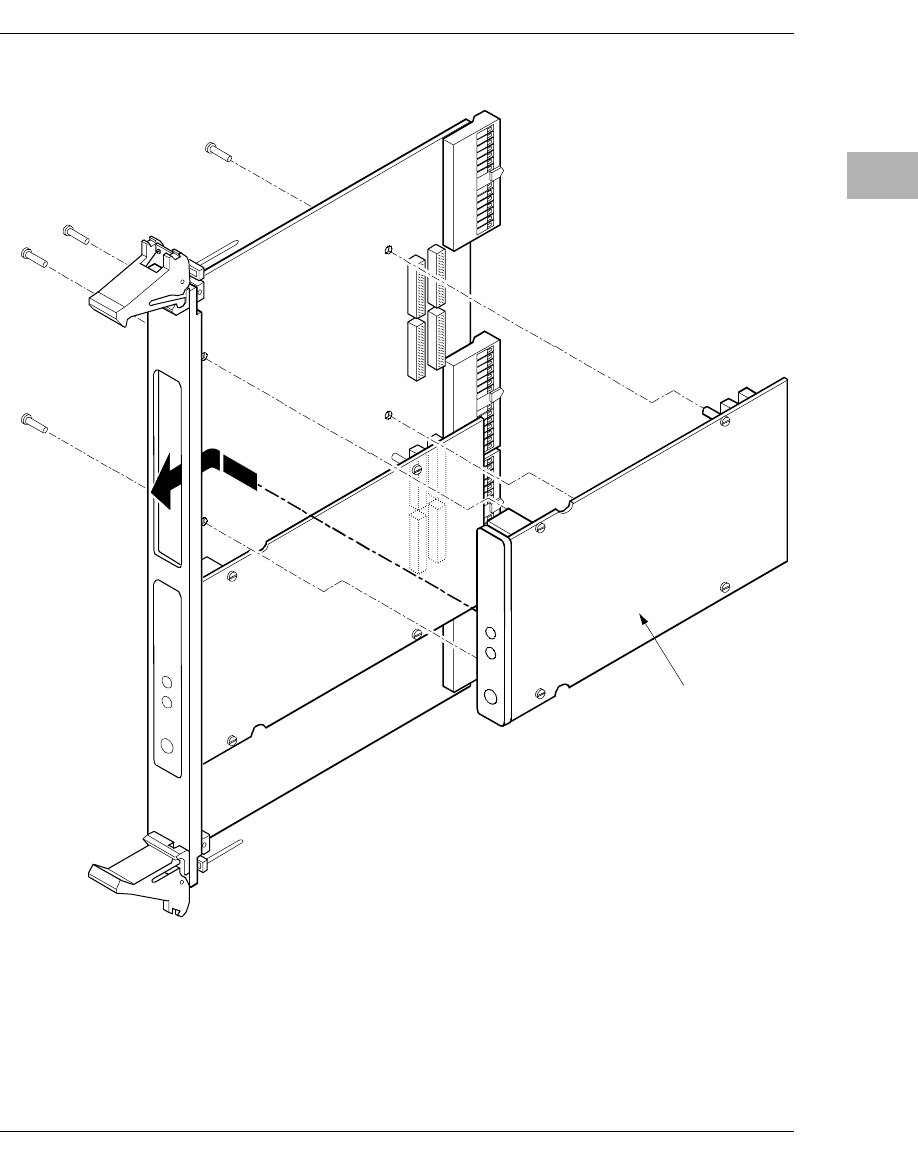
3-4 Computer Group Literature Center Web Site
CPX8540 Carrier Card
3
Connector Pinouts
The tables in this section provide the connector pinout information for the
rear connectors on the carrier card.
Table 3-1. CPCI J3 I/O Connector Pinout
ROW A ROW B ROW C ROW D ROW E
14 +3.3V +3.3V +3.3V +5V +5V 14
13 PMC1IO5 PMC1IO4 PMC1IO3 PMC1IO2 PMC1IO1 13
12 PMC1IO10 PMC1IO9 PMC1IO8 PMC1IO7 PMC1IO6 12
11 PMC1IO15 PMC1IO14 PMC1IO13 PMC1IO12 PMC1IO11 11
10 PMC1IO20 PMC1IO19 PMC1IO18 PMC1IO17 PMC1IO16 10
9 PMC1IO25 PMC1IO24 PMC1IO23 PMC1IO22 PMC1IO21 9
8 PMC1IO30 PMC1IO29 PMC1IO28 PMC1IO27 PMC1IO26 8
7 PMC1IO35 PMC1IO34 PMC1IO33 PMC1IO32 PMC1IO31 7
6 PMC1IO40 PMC1IO39 PMC1IO38 PMC1IO37 PMC1IO36 6
5 PMC1IO45 PMC1IO44 PMC1IO43 PMC1IO42 PMC1IO41 5
4 PMC1IO50 PMC1IO49 PMC1IO48 PMC1IO47 PMC1IO46 4
3 PMC1IO55 PMC1IO54 PMC1IO53 PMC1IO52 PMC1IO51 3
2 PMC1IO60 PMC1IO59 PMC1IO58 PMC1IO57 PMC1IO56 2
1 V(I/O) PMC1IO64 PMC1IO63 PMC1IO62 PMC1IO61 1
NOTE: PMC1IO* signals are those connected to the lower PMC slot, or slot 1.
Table 3-2. CPCI J5 I/O Connector Pinout
ROW A ROW B ROW C ROW D ROW E
13 PMC2IO5 PMC2IO4 PMC2IO3 PMC2IO2 PMC2IO1 13
12 PMC2IO10 PMC2IO9 PMC2IO8 PMC2IO7 PMC2IO6 12
11 PMC2IO15 PMC2IO14 PMC2IO13 PMC2IO12 PMC2IO11 11
Connector Pinouts
http://www.motorola.com/computer/literature 3-5
3
10 PMC2IO20 PMC2IO19 PMC2IO18 PMC2IO17 PMC2IO16 10
9 PMC2IO25 PMC2IO24 PMC2IO23 PMC2IO22 PMC2IO21 9
8 PMC2IO30 PMC2IO29 PMC2IO28 PMC2IO27 PMC2IO26 8
7 PMC2IO35 PMC2IO34 PMC2IO33 PMC2IO32 PMC2IO31 7
6 PMC2IO40 PMC2IO39 PMC2IO38 PMC2IO37 PMC2IO36 6
5 PMC2IO45 PMC2IO44 PMC2IO43 PMC2IO42 PMC2IO41 5
4 PMC2IO50 PMC2IO49 PMC2IO48 PMC2IO47 PMC2IO46 4
3 PMC2IO55 PMC2IO54 PMC2IO53 PMC2IO52 PMC2IO51 3
2 PMC2IO60 PMC2IO59 PMC2IO58 PMC2IO57 PMC2IO56 2
1 V(I/O) PMC2IO64 PMC2IO63 PMC2IO62 PMC2IO61 1
NOTE: PMC2IO* signals are those connected to the upper PMC slot, or slot 2.
Table 3-3. PCI 32-bit Interface Connector P11/J11, P21/J21
Pin# Signal Name Signal Name Pin #
1 TCK -12V 2
3 GND INTA# 4
5INTB# INTC# 6
7 BUSMODE1# +5V 8
9 INTD# PCI-RSVD* 10
11 GND PCI-RSVD* 12
13 CLK GND 14
15 GND GNT# 16
17 REQ# +5V 18
19 V (I/O) AD[31] 20
21 AD[28] AD[27] 22
23 AD[25] GND 24
Table 3-2. CPCI J5 I/O Connector Pinout (continued)
3-6 Computer Group Literature Center Web Site
CPX8540 Carrier Card
325 GND C/BE[3]# 26
27 AD[22] AD[21] 28
29 AD[19] +5V 30
31 V (I/O) AD[17] 32
33 FRAME# GND 34
35 GND IRDY# 36
37 DEVSEL# +5V 38
39 GND LOCK# 40
41 SDONE# SBO# 42
43 PAR GND 44
45 V (I/O) AD[15] 46
47 AD[12] AD[11] 48
49 AD[09] +5V 50
51 GND C/BE[0]# 52
53 AD[06] AD[05] 54
55 AD[04] GND 56
57 V (I/O) AD[03] 58
59 AD[02] AD[01] 60
61 AD[00] +5V 62
63 GND REQ64# 64
Table 3-3. PCI 32-bit Interface Connector P11/J11, P21/J21 (continued)
Pin# Signal Name Signal Name Pin #
Connector Pinouts
http://www.motorola.com/computer/literature 3-7
3
Table 3-4. PCI 32-bit Interface Connector P12/J12, P22/J22
Pin# Signal Name Signal Name Pin #
1+12V TRST# 2
3TMS TDO 4
5 TDI GND 6
7 GND PCI-RSVD* 8
9 PCI-RSVD* PCI-RSVD* 10
11 BUSMODE2# +3.3V 12
13 RST# BUSMODE3# 14
15 +3.3V BUSMODE4# 16
17 PCI-RSVD* GND 18
19 AD[30] AD[29] 20
21 GND AD[26] 22
23 AD[24] +3.3V 24
25 IDSEL AD[23] 26
27 +3.3V AD[20] 28
29 AD[18] GND 30
31 AD[16] C/BE[2]# 32
33 GND PMC-RSVD 34
35 TRDY# +3.3V 36
37 GND STOP# 38
39 PERR# GND 40
41 +3.3V SERR# 42
43 C/BE[1]# GND 44
45 AD[14] AD[13] 46
47 GND AD[10] 48
49 AD[08] +3.3V 50
3-8 Computer Group Literature Center Web Site
CPX8540 Carrier Card
351 AD[07] PMC-RSVD 52
53 +3.3V PMC-RSVD 54
55 PMC-RSVD GND 56
57 PMC-RSVD PMC-RSVD 58
59 GND PMC-RSVD 60
61 ACK64# +3.3V 62
63 GND PMC-RSVD 64
Table 3-5. PCI 64 bit PCI extension on PMC Connector J13, J23
Pin# Signal Name Signal Name Pin #
1 - GND 2
3 GND C/BE7# 4
5 C/BE6# C/BE5# 6
7 C/BE4# GND 8
9 V(I/O) PAR64 10
11 AD63 AD62 12
13 AD61 GND 14
15 GND AD60 16
17 AD59 AD58 18
19 AD57 GND 20
21 V(I/O) AD56 22
23 AD55 AD54 24
25 AD53 GND 26
27 GND AD52 28
29 AD51 AD50 30
Table 3-4. PCI 32-bit Interface Connector P12/J12, P22/J22 (continued)
Pin# Signal Name Signal Name Pin #

Connector Pinouts
http://www.motorola.com/computer/literature 3-9
3
31 AD49 GND 32
33 GND AD48 34
35 AD47 AD46 36
37 AD45 GND 38
39 V(I/O) AD44 40
41 AD43 AD42 42
43 AD41 GND 44
45 GND AD40 46
47 AD39 AD38 48
49 AD37 GND 50
51 GND AD36 52
53 AD35 AD34 54
55 AD33 GND 56
57 V(I/O) AD32 58
59--60
61 - GND 62
63 GND - 64
Table 3-6. User-Defined I/O PCI Interface Connector P14/J14, P24/J24
Pin# Signal Name
1-64 I/O
Table 3-5. PCI 64 bit PCI extension on PMC Connector J13, J23
Pin# Signal Name Signal Name Pin #

4-1
4
4PMC Modules
Overview
This chapter provides reference information for the PMC module
supported in the CPX8216 system.
SCSI-2 Controller PMC
The SCSI-2 controller provides fast and wide, single-ended, SCSI-2
(Small Computer System Interface-2) high throughput connectivity for
host carrier boards equipped with PMC (PCI Mezzanine Card)
connections.
The PMC adapter is a plug-and-play device with systems that are
compliant with the PCI Local Bus Specification (revision 2.0).
This controller has the following capabilities:
❏Single-wide PMC module
❏32-bit wide PCI bus support
❏128Kb onboard flash memory
❏20 Mbps Fast and Wide SCSI-2
❏Single-ended SCSI-2 interfaces
❏Front and rear User I/O
❏68-pin front panel connector
❏64-pin JN4/PN4 rear connector
❏+3.3V and +5V signaling
❏Compliance to PCI local bus specification (Revision 2.0)
4-2 Computer Group Literature Center Web Site
PMC Modules
4
The following figure shows the PMC150 component layout and front
panel.
4118 0702
PN2
S1
U13U14U15
JP40
U1
U5
U31
PN4
PN1
Switch Settings
http://www.motorola.com/computer/literature 4-3
4
Switch Settings
Use this table as a guideline for configuring the 6-position dip switch on
your PMC.
Terminators - The SCSI bus (cable) must be properly terminated at each
end of the bus. The first and last device on the bus should be the only
devices that are set to terminate the bus.
Terminator Power - The SCSI terminators require adequate voltage to
properly terminate the SCSI bus. All SCSI host adapters on the bus should
be set to supply terminator power; and where possible, be located at the
end of the bus and serve as bus terminators.The terminator resistors must
be present on the first and last device on the bus only.
For further information on this PMC, visit the Technobox, Inc. web site at
http://www.technobox.com.
Table 4-1. PMC Switch Settings
Switch On Function Off Function Default
1 Use INTA No Use INTA On
2 Use INTB No Use INTB Off
3 Use INTC No Use INTC Off
4 Use INTD No Use INTD Off
5 TERM Enable TERM Disable On
6 Little Endian Big Endian On
Configure the Big/Little endian mode to your appropriate application for proper
software operation.
Make sure only one INTx line switch is in the ON position.
Enable TERM ENAB is On only if this SCSI controller is physically at the end
of the SCSI bus. If the SCSI controller is in any other position on the bus, TERM
ENAB must be in the OFF mode.

4-4 Computer Group Literature Center Web Site
PMC Modules
4
Connector Pin Assignments
The table below provides the connector pin assignments for the SCSI
connector on the PMC adapter. The connector uses a 68-pin Euro-style
SCSI cable, either shielded for external or internal cabinet applications or
non-shielded for internal cabinet applications only. For rear I/O, a 64-pin
conductor cable is used. The pin assignments are also provided in the
following table.
Table 4-2. PMC Pin Assignments
Signal
name
68-Pin
Connector
Number
64-Pin
Conductor
Cable
Number
68-Pin
Connector
Number Signal
name
Ground
Ground
Ground
Ground
Ground
Ground
Ground
Ground
Ground
Ground
Ground
1
2
3
4
5
6
7
8
9
10
11
1
3
5
7
9
11
13
15
17
19
21
2
4
6
8
10
12
14
16
18
20
22
35
36
37
38
39
40
41
42
43
44
45
-DB(12)
-DB(13)
-DB(14)
-DB(15)
-DB(P1)
-DB(0)
-DB(1)
-DB(2)
-DB(3)
-DB(4)
-DB(5)
Ground
Ground
Ground
Ground
Ground
TERMPWR
TERMPWR
Reserved
Ground
Ground
Ground
Ground
12
13
14
15
16
17
18
19
20
21
22
23
23
25
27
29
31
33
N/C
N/C
35
37
39
41
24
26
28
30
32
34
N/C
N/C
36
38
40
42
46
47
48
49
50
51
52
53
54
55
56
57
-DB(6)
-DB(7)
-DB(P)
Ground
Ground
TERMPWR
TERMPWR
Reserved
Ground
-ATN
Ground
-BSY
Connector Pin Assignments
http://www.motorola.com/computer/literature 4-5
4
Ground
Ground
Ground
Ground
Ground
Ground
Ground
Ground
Ground
Ground
Ground
24
25
26
27
28
29
30
31
32
33
34
43
45
47
49
51
53
55
57
59
61
63
44
46
48
50
52
54
56
58
60
62
64
58
59
60
61
62
63
64
65
66
67
68
-ACK
-RST
-MSG
-SEL
-C/D
-REQ
-I/O
-DB(8)
-DB(9)
-DB(10)
-DB(11)
Table 4-2. PMC Pin Assignments (continued)
Signal
name
68-Pin
Connector
Number
64-Pin
Conductor
Cable
Number
68-Pin
Connector
Number Signal
name
5-1
5
5Transition/Bridge Modules
Overview
This chapter provides reference information for the various transition and
bridge modules supported in the CPX8216 system.
The correct jumper setting and pin-out information is provided for each
module.
Note The CPX750HATM is also used with the MCP750HA in some
chassis configurations.
Your system may not contain all boards listed in this chapter, or
it may contain third-party boards that are not listed in this
chapter. For information about third-party boards, refer to the
board manufacturer’s documentation.
The following table lists the modules covered in this chapter:
CPX750HATM Transition Module
The CPX750HATM transition module provides the interface between the
standard Parallel Port, EIDE port, floppy port, keyboard/mouse port, Serial
Port connectors, and the CPX750HA CompactPCI Single Board Computer
module.
Table 5-1. System Components
Topic: Page:
CPX750HATM Transition Module 5-1
CPV5350TM80 Transition Module 5-29

5-2 Computer Group Literature Center Web Site
Transition/Bridge Modules
5
The CPX750HATM transition module includes:
❏Industry-standard connectors for these interfaces:
– Two asynchronous RJ-45 serial ports (DTE)
– Two asynchronous/synchronous HD-26 serial ports, labeled
Serial 3 and Serial 4 on the face plate, which can be configured
for EIA-232-D, EIA-530, V.35, or X.21 interfaces (DCE or
DTE) through the installation of Motorola’s Serial Interface
Modules (SIMs)
– One parallel port (IEEE Standard 1284-I compliant)
– One combination keyboard/mouse port
❏Two 60-pin Serial Interface Module (SIM) connectors for
configuring the asynchronous/synchronous serial ports
❏One 40-pin header for EIDE port
❏One 34-pin header for floppy port
❏Two 64-pin headers for PMCIO (1 ground pin provided with each
PMCIO signal)
Figure 5-1 on page 5-3 shows the CPX750HATM transition module
component layout and the front panel. See Connectors on page 5-4 for a
list of the front panel port connectors.
Serial Ports 3 and 4 Default Configuration
The CPX750HATM serial ports 3 and 4 are factory configured as follows:
❏Serial Port 3: DTE (with SIMM 01-W3877B01A installed)
❏Serial Port 4: DCE (with SIMM 01-W3876B01A installed)
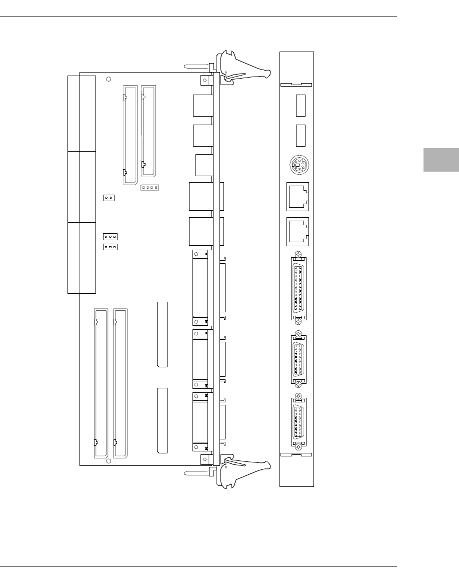
Serial Ports 3 and 4 Default Configuration
http://www.motorola.com/computer/literature 5-3
5
Figure 5-1. CPX750HATM Transition Module
2214 9804
COM 1
1
USB 1 SERIAL 4
2
41
J1 59
60
J11 J18 J19
41
82
71
USB 0
J14
J8
2
1
64
63
J21 J9 J13
2
1
1
2J23 59
60
2
1
64
63
J2
3
1
3
1
2
1
40
39
J15
2
1
34
33
J17
J10
82
71
J7
17 1
34 18
J24
13 1
26 14 J6
13 1
26 14
COM 2 SERIAL 3PARALLEL
KB/MS
J16
J3 J5
J4
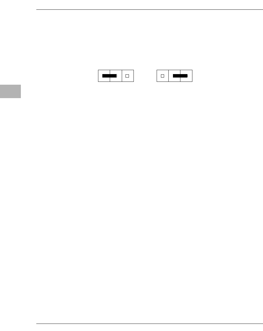
5-4 Computer Group Literature Center Web Site
Transition/Bridge Modules
5
Serial Port Interface Jumper (J8 and J9)
J8 (for serial port 3) and J9 (for serial port 4) set the serial ports to either
DTE or DCE communication. For more information about configuring the
serial port, see Installing the Serial Interface Modules on page 5-16.
Figure 5-2. Serial Port Interface Jumper (J9) Settings
Connectors
Refer to Figure 5-1 on page 5-3 for the location of the following connectors
Backplane Connectors (J3/J4/J5)
I/O signals and power are provided to the CPX750HATM from the
CPX750 through CompactPCI connectors J3 and J5. The J4 connector is
for physical alignment purposes only and has no functional pin
connections or assignments.
Connector J3 is a 95-pin AMP Z-pack 2mm hard metric type B connector.
This connector routes the I/O signals for the PMC I/O and serial channels.
The pin assignments for J3 are as follows (outer row F is assigned and used
as ground pins but is not shown in the table):
Connector J4 is a 110-pin 2mm hard metric type A connector. This
connector is placed on the board for alignment purposes only. The keying
tabs on the type A connector assist with alignment of pins in the backplane
connector during insertion of the boards. No signals are connected to J4
except the row F ground pins.
Connector J5 is a 110-pin AMP Z-pack 2mm hard metric type B connector.
This connector routes the I/O signals for the IDE (secondary port), the
keyboard, the mouse, the two USB ports, and the printer ports. The pin
11650 9610
123 123
DCE
DTE
Connectors
http://www.motorola.com/computer/literature 5-5
5
assignments for J5 are as follows (the outer row F is assigned and used as
ground pins but is not shown in the table):
Table 5-2 and Table 5-3 provide the pin assignments and signal mnemonics
for connectors J3 and J5 (J4 is not shown)
Table 5-2. J3 User I/O Connector
ROW A ROW B ROW C ROW D ROW E
19 Reserved +12V -12V RXD3 RXD4 19
18 Reserved GND RXC3 GND RXC4 18
17 Reserved MXCLK MXDI MXSYNC_L MXDO 17
16 Reserved GND TXC3 GND TXC4 16
15 Reserved Reserved Reserved TXD3 TXD4 15
14 +3.3V +3.3V +3.3V +5V +5V 14
13 PMCIO5 PMCIO4 PMCIO3 PMCIO2 PMCIO1 13
12 PMCIO10 PMCIO9 PMCIO8 PMCIO7 PMCIO6 12
11 PMCIO15 PMCIO14 PMCIO13 PMCIO12 PMCIO11 11
10 PMCIO20 PMCIO19 PMCIO18 PMCIO17 PMCIO16 10
9PMCIO25 PMCIO24 PMCIO23 PMCIO22 PMCIO21 9
8PMCIO30 PMCIO29 PMCIO28 PMCIO27 PMCIO26 8
7PMCIO35 PMCIO34 PMCIO33 PMCIO32 PMCIO31 7
6PMCIO40 PMCIO39 PMCIO38 PMCIO37 PMCIO36 6
5PMCIO45 PMCIO44 PMCIO43 PMCIO42 PMCIO41 5
4PMCIO50 PMCIO49 PMCIO48 PMCIO47 PMCIO46 4
3PMCIO55 PMCIO54 PMCIO53 PMCIO52 PMCIO51 3
2PMCIO60 PMCIO59 PMCIO58 PMCIO57 PMCIO56 2
1VIO PMCIO64 PMCIO63 PMCIO62 PMCIO61 1
Row F is assigned and used as ground pins but is not shown in the table
5-6 Computer Group Literature Center Web Site
Transition/Bridge Modules
5
Asynchronous Serial Port Connectors (J10 and J11)
The interface for the asynchronous serial ports, COM1 and COM2, is
provided with two RJ-45 connectors, J11 and J10. The connector shields
Table 5-3. J5 User I/O Connector
ROW A ROW B ROW C ROW D ROW E
22 Reserved GND Reserved +5V SPKROC_L 22
21 KBDDAT KBDCLK KBAUXVCC AUXDAT AUXCLK 21
20 Reserved Reserved Reserved GND Reserved 20
19 STB_L GND UVCC0 Reserved Reserved 19
18 AFD_L Reserved Reserved GND UVCC1 18
17 PD2 INIT_L PD1 ERR_L PD0 17
16 PD6 PD5 PD4 PD3 SLIN_L 16
15 SLCT PE BUSY ACK_L PD7 15
14 RTSa CTSa RIa GND DTRa 14
13 DCDa +5V RXDa DSRa TXDa 13
12 RTSb CTSb RIb +5V DTRb 12
11 DCDb GND RXDb DSRb TXDb 11
10 TR0_L WPROT_L RDATA_L HDSEL_L DSKCHG_L 10
9MTR1_L DIR_L STEP_L WDATA_L WGATE_L 9
8Reserved INDEX_L MTR0_L DS1_L DS0_L 8
7CS1FX_L CS3FX_L DA1 Reserved Reserved 7
6Reserved GND Reserved DA0 DA2 6
5DMARQ IORDY DIOW_L DMACK_L DIOR_L 5
4DD14 DD0 GND DD15 INTRQ 4
3DD3 DD12 DD2 DD13 DD1 3
2DD9 DD5 DD10 DD4 DD11 2
1RESET_L DRESET_L DD7 DD8 DD6 1
Row F is assigned and used as ground pins but is not shown in the table
Connectors
http://www.motorola.com/computer/literature 5-7
5
for these ports are tied to chassis ground. The pin assignments and signal
mnemonics for these connectors are listed in the next table.
Asynchronous/Synchronous Serial Port Connectors (J6 and J24)
The interface for the asynchronous/synchronous serial ports 3 and 4 is
provided by two HD-26 connectors, J6 and J24. The connector shields for
these ports are tied to chassis ground.
The pin assignments and signal mnemonics for Serial Port 3 are listed in
Table 5-5, and the pin assignments and signal mnemonics for Serial Port 4
are listed in Table 5-6.
Table 5-4. COM1 (J11) and COM2 (J10)
Pin Signal
1DCD
2RTS
3 GND
4TXD
5RXD
6 GND
7CTS
8DTR
Table 5-5. Serial Port 3 (J6)
Pin Signal Signal Pin
1 No Connect SP3_P14 14
2 TXD3 TXCI3 15
3 RXD3 SP3_P16 16
4RTS3 RXCI3 17
5 CTS3 LLB3 18
5-8 Computer Group Literature Center Web Site
Transition/Bridge Modules
5
6 DSR3 SP3_P19 19
7 GND DTR3 20
8DCD3 RLB3 21
9 SP3_P9 RI3 22
10 SP3_P10 SP3_P23 23
11 SP3_P11 TXCO3 24
12 SP3_P12 TM3 25
13 SP3_P13 SP3_P26 26
Table 5-5. Serial Port 3 (J6) (continued)
Pin Signal Signal Pin
Table 5-6. Serial Port 4 (J24)
Pin Signal Signal Pin
1 No Connect SP4_P14 14
2 TXD4 TXCI4 15
3 RXD4 SP4_P16 16
4RTS4 RXCI4 17
5 CTS4 LLB4 18
6 DSR4 SP4_P19 19
7 GND DTR4 20
8DCD4 RLB4 21
9 SP4_P9 RI4 22
10 SP4_P10 SP4_P23 23
11 SP4_P11 TXCO4 24
12 SP4_P12 TM4 25
13 SP4_P13 SP4_P26 26
Connectors
http://www.motorola.com/computer/literature 5-9
5
Parallel I/O Port Connector (J7)
The interface for the parallel port is a standard IEEE P1284-C, 36-pin
connector, J7. The functionality of each signal depends on the mode of
operation of this bidirectional Parallel Peripheral Interface. Refer to the
IEEE P1284 D2.00 Standard for a complete description of each signal
function. The connector shield is tied to chassis ground.
The pin assignments and signal mnemonics for this connector are listed in
the next table.
Table 5-7. Parallel I/O Connector (J7)
Pin Signal Signal Pin
1 PRBSY GND 19
2 PRSEL GND 20
3 PRACK_ GND 21
4 PRFAULT_ GND 22
5 PRPE GND 23
6 PRD0 GND 24
7 PRD1 GND 25
8 PRD2 GND 26
9 PRD3 GND 27
10 PRD4 GND 28
11 PRD5 GND 29
12 PRD6 GND 30
13 PRD7 GND 31
14 PRINIT_ GND 32
15 PRSTB_ GND 33
16 SELIN_ GND 34
17 AUTOFD_ GND 35
18 Pull-up No Connect 36
5-10 Computer Group Literature Center Web Site
Transition/Bridge Modules
5
Keyboard/Mouse Connector (J16)
The Keyboard/Mouse interface is provided by a 6-pin circular DIN
connector. To use the keyboard function only, a keyboard may be
connected directly to this connector. To use both the keyboard and the
mouse functions, use the Y-adapter cable provided with the
CPX750HATM. Refer to the following table for pin assignments.
USB Connectors (J19 and J18)
The standard version of the CPX750 routes the USB port signals only to
the CPX750 front panel USB connectors J18 and J17. Therefore the USB
port connectors (J19 and J18) on the CPX750HATM are not active. The
USB ports can be routed to the CPX750HATM using an alternate build
option of the CPX750. Contact your local Motorola Sales office for details.
Table 5-8. Keyboard/Mouse Connector (J16)
Pin Signal
1KBD DAT
2MSDAT
3 GND
4 +5Vdc Fused
5 KBDCLK
6MSCLK
Connectors
http://www.motorola.com/computer/literature 5-11
5
EIDE Connector (J15)
The CPX750HATM provides a 40-pin header (J15) to interface to the
CPX750 secondary EIDE port. The pin assignments and signal mnemonics
for this connector are listed in the next table.
Table 5-9. EIDE Connector (J15)
Pin Signal Signal Pin
1 DRESET_L GND 2
3 DD7 DD8 4
5 DD6 DD9 6
7 DD5 DD10 8
9 DD4 DD11 10
11 DD3 DD12 12
13 DD2 DD13 14
15 DD1 DD14 16
17 DD0 DD15 18
19 GND No Connect 20
21 DMARQ GND 22
23 DIOW_L GND 24
25 DIOR_L GND 26
27 IORDY No Connect 28
29 DMACK_L GND 30
31 INTRQ No Connect 32
33 DA1 No Connect 34
35 DA0 DA2 36
37 CS1FX_L CS3FX_L 38
39 No Connect GND 40
5-12 Computer Group Literature Center Web Site
Transition/Bridge Modules
5
Floppy Port Connector (J17)
The CPX750HATM provides a 34-pin header (J17) to interface to a floppy
disk drive. The pin assignments and signal mnemonics for this connector
are listed in the next table.
+5Vdc Power Connector (J14)
The CPX750HATM has a 4-pin header that can be used to provide +5Vdc
power to offboard devices. This power is derived from the fused +5Vdc
power on the CPX750. Any external device powered from this connector
Table 5-10. Floppy Connector (J17)
Pin Signal Signal Pin
1 GND No Connect 2
3 GND No Connect 4
5 GND No Connect 6
7 No Connect INDEX_L 8
9 GND MTR0_L 10
11 GND DS1_L 12
13 No Connect DS0_L 14
15 GND MTR1_L 16
17 No Connect DIR_L 18
19 GND STEP_L 20
21 GND WDATA_L 22
23 GND WGATE_L 24
25 GND TR0_L 26
27 GND WPROT_L 28
29 GND RDATA_L 30
31 GND HDSEL_L 32
33 GND DSKCHG_L 34
Connectors
http://www.motorola.com/computer/literature 5-13
5
must not draw more than 200mA. The pin assignments are listed in the
following table.
Speaker Output Connector (J13)
The 2-pin header (J13) provides connection to an external speaker from the
CPX750 PCB Counter 2 output. The speaker driver, located on the
CPX750 PCB, consists of a 500 mA (max) current sink transistor in series
with a 33 ohm resistor. The pin assignments are listed in the following
table.
Table 5-11. +5Vdc Power Connector (J14)
Pin Signal
1 +5Vdc
2 GND
3 GND
4 No Connect
Table 5-12. Speaker Output Connector (J13)
Pin Signal
1 GND
2 SPKROC_L
5-14 Computer Group Literature Center Web Site
Transition/Bridge Modules
5
PMC I/O Connectors
The PMC I/O connectors consist of two 64-pin header connectors J2 and
J21. The pin assignments and signal mnemonics for these connectors are
listed below.
Table 5-13. PMC I/O Connector (J2)
Pin Signal Signal Pin
1 GND PMCIO1 2
3 GND PMCIO2 4
5 GND PMCIO3 6
7 GND PMCIO4 8
9 GND PMCIO5 10
11 GND PMCIO6 12
13 GND PMCIO7 14
15 GND PMCIO8 16
17 GND PMCIO9 18
19 GND PMCIO10 20
21 GND PMCIO11 22
23 GND PMCIO12 24
25 GND PMCIO13 26
27 GND PMCIO14 28
29 GND PMCIO15 30
31 GND PMCIO16 32
33 GND PMCIO17 34
35 GND PMCIO18 36
37 GND PMCIO19 38
39 GND PMCIO20 40
41 GND PMCIO21 42
Connectors
http://www.motorola.com/computer/literature 5-15
5
43 GND PMCIO22 44
45 GND PMCIO23 46
47 GND PMCIO24 48
49 GND PMCIO25 50
51 GND PMCIO26 52
53 GND PMCIO27 54
55 GND PMCIO28 56
57 GND PMCIO29 58
59 GND PMCIO30 60
61 GND PMCIO31 62
63 GND PMCIO32 64
Table 5-13. PMC I/O Connector (J2) (continued)
Pin Signal Signal Pin
Table 5-14. PMC I/O Connector (J21)
Pin Signal Signal Pin
1 GND PMCIO33 2
3 GND PMCIO34 4
5 GND PMCIO35 6
7 GND PMCIO36 8
9 GND PMCIO37 10
11 GND PMCIO38 12
13 GND PMCIO39 14
15 GND PMCIO40 16
17 GND PMCIO41 18
19 GND PMCIO42 20
21 GND PMCIO43 22
5-16 Computer Group Literature Center Web Site
Transition/Bridge Modules
5
Installing the Serial Interface Modules
Configure the serial ports 3 and 4 for the required interface by installing
the appropriate SIM.
23 GND PMCIO44 24
25 GND PMCIO45 26
27 GND PMCIO46 28
29 GND PMCIO47 30
31 GND PMCIO48 32
33 GND PMCIO49 34
35 GND PMCIO50 36
37 GND PMCIO51 38
39 GND PMCIO52 40
41 GND PMCIO53 42
43 GND PMCIO54 44
45 GND PMCIO55 46
47 GND PMCIO56 48
49 GND PMCIO57 50
51 GND PMCIO58 52
53 GND PMCIO59 54
55 GND PMCIO60 56
57 GND PMCIO61 58
59 GND PMCIO62 60
61 GND PMCIO63 62
63 GND PMCIO64 64
Table 5-14. PMC I/O Connector (J21) (continued)
Pin Signal Signal Pin
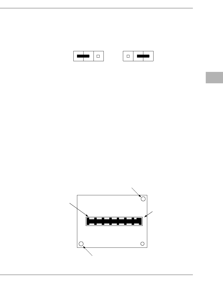
Installing the Serial Interface Modules
http://www.motorola.com/computer/literature 5-17
5
Prior to installing the SIMs, set the jumpers on header J8 (for Serial Port
3) and header J9 (for Serial Port 4) for either DCE or DTE. Set the jumper
to position 1-2 if the SIM is for a DTE interface. Set the jumper to position
2-3 if the SIM is for a DCE interface.
You must set the jumpers and install the SIMs prior to installing the
CPX750HATM transition module in the system chassis.
The SIMs plug into connector J23 (for Serial Port 3) or J1 (for Serial Port
4) on the CPX750HATM transition module.
Install the SIMs on the CPX750HATM transition module per the following
procedure:
1. Align the SIM so that P1 on the SIM lines up with the appropriate SIM
connector (J23 for Serial Port 3 or J1 for Serial Port 4) on the transition
module. Note the position of the alignment key on P1. See the next
figure.
2. Place the SIM onto the transition module SIM connector, making sure
that the mounting holes also line up with the standoffs on the transition
module.
123 123
DCE
DTE
Mounting Hole
Mounting Hole
Alignment
P1
Key
11637 9610

5-18 Computer Group Literature Center Web Site
Transition/Bridge Modules
5
3. Gently press the top of the SIM to seat it on the transition module SIM
connector. If the SIM does not seat with gentle pressure, re-check the
alignment of the connectors.
Note Do not force the SIM onto the transition module.
4. Secure the SIM to the transition module standoffs with the two
Phillips-head screws provided. Do not over tighten the screws.
Port Configuration Diagrams
The following sections describe the configurations for COM1 and COM2
asynchronous serial ports.
COM1 and COM2 Asynchronous Serial Ports
The asynchronous serial port (COM1 and COM2) configuration is shown
in Figure 5-3 on page 5-19.
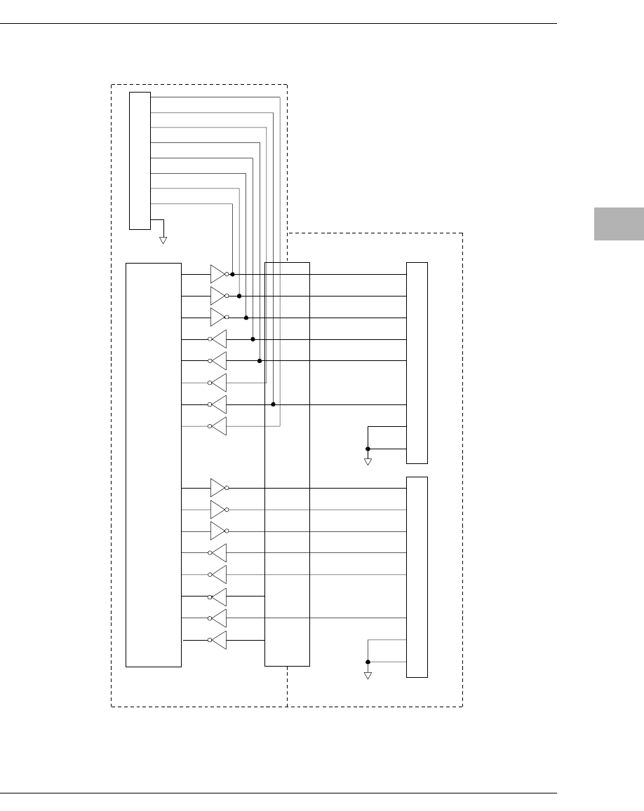
Port Configuration Diagrams
http://www.motorola.com/computer/literature 5-19
5
Figure 5-3. DTE Port Configuration (COM1 and COM2)
CPX750
2105 9710
4
2
5
7
8
1
3
6
COM1
COM2
4
2
5
7
8
1
3
6
9
1
8
2
6
4
7
3
5
COM1
(Front
Panel)
SOUT1
RTS1#
DTR1#
SIN1
RI1#
CTS1#
DSR1#
DCD1#
PC87307
SOUT2
RTS2#
DTR2#
SIN2
RI2#
CTS2#
DSR2#
DCD2
J5
J15
TXD
RTS
DTR
RXD
CTS
DCD
TXD
RTS
DTR
RXD
CTS
DCD
(J11)
(J10)
GND
GND
Transition Module
CPX750HATM

5-20 Computer Group Literature Center Web Site
Transition/Bridge Modules
5
Asynchronous/Synchronous Serial Ports
The asynchronous/synchronous serial port (Port 3 and Port 4) interface
configuration diagrams are on the following pages.
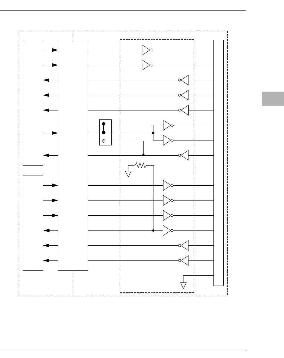
Port Configuration Diagrams
http://www.motorola.com/computer/literature 5-21
5
Figure 5-4. EIA-232-D DCE Port Configuration (Ports 3 and 4)
TXD
RTS#
RXD
CTS#
RTXC
TRXC
EIA-232-D DCE SIM
DSR#
DTR#
LLB#
RLB#
DCD#
RI#
TM#
8
25
22
21
20
18
7
3
5
2
15
4
17
24
6
Z85230 SCC
Z8536 CIO
DB25
J3/MX
RXD
CTS#
TXD
RTS#
DTR#
TXC
RXC#
ETXC
DCD#
TM#
RI#
DSR#
RL
LL
GND
J8, J9
3
2
1
2106 971
Transition Module
CPX750HATM
CPX750
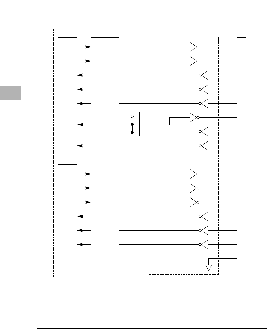
5-22 Computer Group Literature Center Web Site
Transition/Bridge Modules
5
Figure 5-5. EIA-232-D DTE Port Configuration (Ports 3 and 4)
TXD
RTS#
RXD
CTS#
RTXC
TRXC
EIA-232-D DTE SIM
DSR#
DTR#
LLB#
RLB#
DCD#
RI#
TM#
20
18
21
22
8
25
7
2
4
3
24
5
15
17
6
Z85230 SCC
Z8536 CIO
DB25
J3/MX
TXD
RTS#
RXD
CTS#
DCD#
ETXC
TXC#
RXC
DTR
LL
RL
DSR#
RI#
TM#
GND#
J8, J9
3
2
1
2107 971
Transition Module
CPX750HATM
CPX750
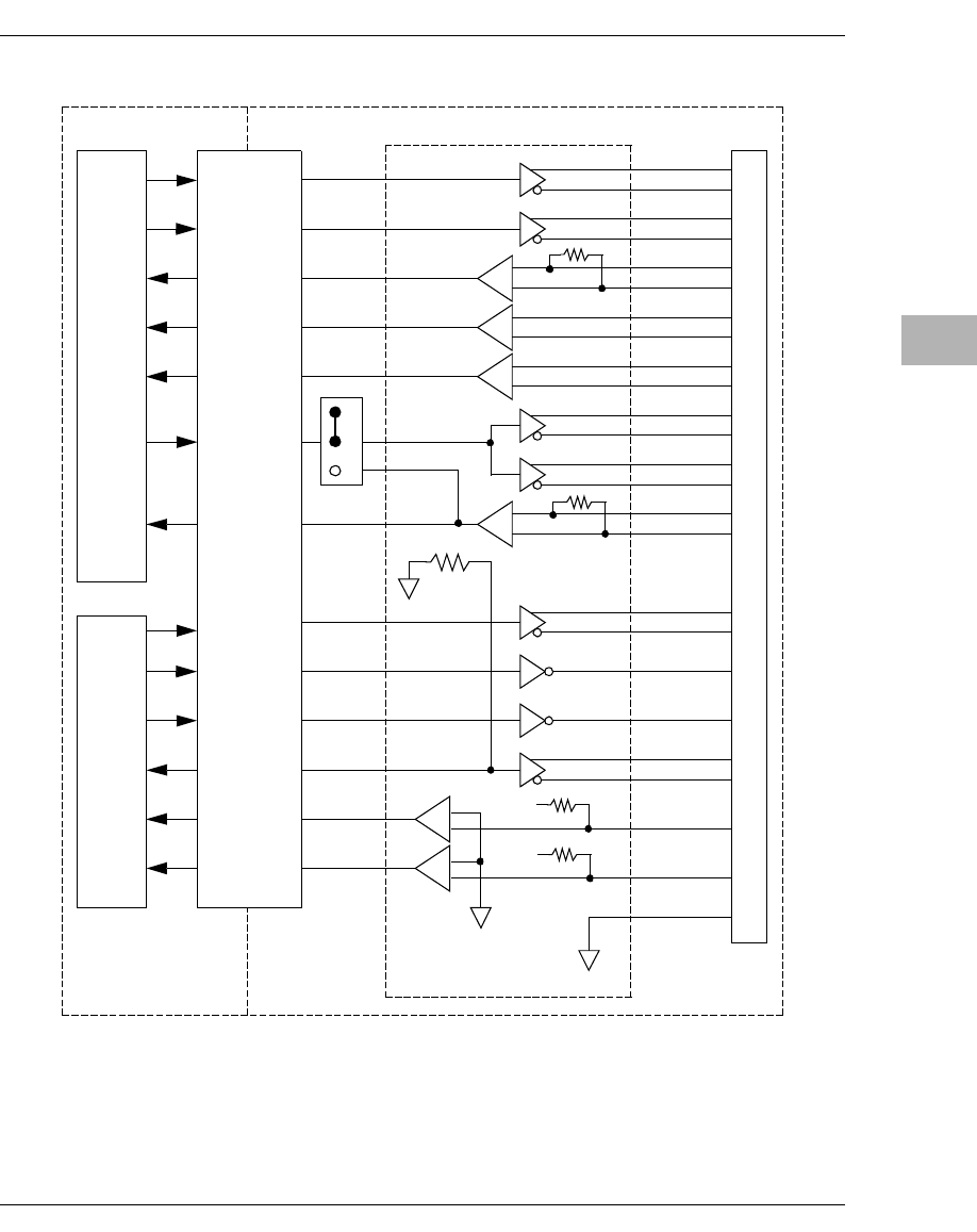
Port Configuration Diagrams
http://www.motorola.com/computer/literature 5-23
5
Figure 5-6. EIA-530 DCE Port Configuration (Ports 3 and 4)
Z85230 SCC
Z8536 CIO
DB25
TXD
RTS_
RXD
CTS_
RTXC
TRXC
DSR_
DTR_
LL_
RL_
DCD_
RI_
TM_
+
-
+
-
+
-
+
-
+
-
-V
-V
RXDB
CTSB
TXDB
RTSB
DTRB
TXCB
RXCB
ETXCB
DCDB
TM
RI
DSRB
RL
LL
GND
RXDA
CTSA
TXDA
RTSA
DTRA
TXCA
RXCA
ETXCA
DCDA
DSRA
J3/MX
20
15
17
25
26
21
18
7
3
5
2
16
13
14
4
19
23
12
9
24
11
8
10
6
22
20
15
17
+
-
2108 971
0
EIA-530-D DCE SIM
J8, J9
3
2
1
Transition Module
CPX750HATM
CPX750
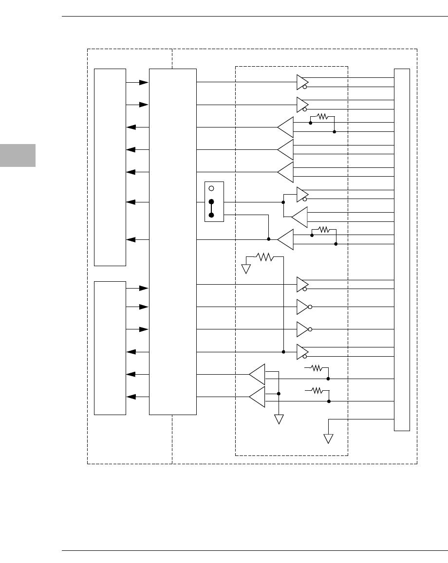
5-24 Computer Group Literature Center Web Site
Transition/Bridge Modules
5
Figure 5-7. EIA-530 DTE Port Configuration (Ports 3 and 4)
Z85230 SCC
Z8536 CIO
DB25
TXD
RTS_
RXD
CTS_
RTXC
TRXC
DSR_
DTR_
LL_
RL_
DCD_
RI_
TM_
+
-
+
-
+
-
+
-
+
-
-V
-V
TXDB
RTSB
RXDB
CTSB
DTRB
ETXCB
TXCB
RXCB
DTRB
LL
RL
DSRB
(R)
TM
GND
TXDA
RTSA
RXDA
CTSA
DTRA
ETXCA
TXCA
RTXCA
DTRA
DSRA
J3/MX
20
15
17
18
21
26
25
7
2
4
3
14
19
16
5
13
10
11
12
17
9
20
23
6
22
8
24
15
+
-
2109 9710
EIA-530-D DTE SIM
J8, J9
3
2
1+
-
Transition Module
CPX750HATM
CPX750
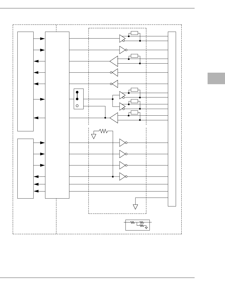
Port Configuration Diagrams
http://www.motorola.com/computer/literature 5-25
5
Figure 5-8. V.35-DCE Port Configuration (Ports 3 and 4)
Z85230 SCC
Z8536 CIO
DB25
V.35-DCE SIM
TXD
RTS_
RXD
DCD_
RTXC
TRXC
DSR_
DTR_
LL_
RL_
CTS_
RI_
TM_
+
-
+
-
RXDB
TXDB
TXCB
RXCB
ETXCB
TM
RI
RL
LL
GND
RXDA
TXDA
TXCA
RXCA
ETXCA
J3/MX
15
17
25
22
21
18
7
3
2
16
14
12
9
24
11
15
17
Term = V.35 Termination Network
CTS 5
Term
Term
Term
RTS 4
DTR 20
DSR 6
DCD 8
2110 971
J8, J9
3
2
1
Term
Term
Transition Module
CPX750HATM
CPX750
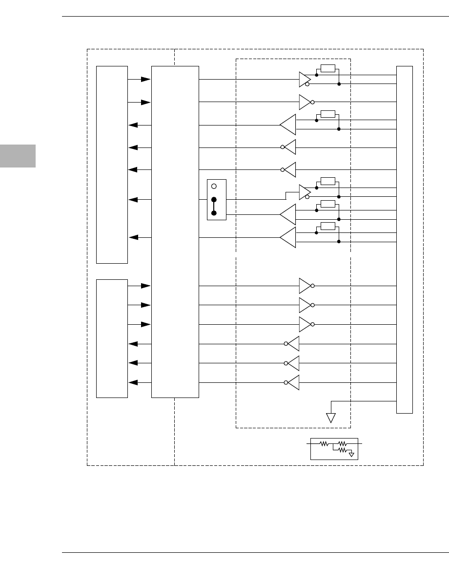
5-26 Computer Group Literature Center Web Site
Transition/Bridge Modules
5
Figure 5-9. V.35-DTE Port Configuration (Ports 3 and 4)
Z85230 SCC
Z8536 CIO
DB25
TXD
RTS_
RXD
CTS_
RTXC
TRXC
DSR_
DTR_
LL_
RL_
DCD_
RI_
TM_
+
-
+
-
TXDB
RXDB
ETXCB
TXCB
RXCB
LL
RL
RI
TM
GND
TXDA
RXDA
ETXCA
TXCA
RXCA
15
17
18
21
22
25
7
2
3
14
16
11
12
17
9
24
15
RTS 4
CTS 5
DCD 8
DSR 6
DTR 20
+
-
J3/MX
V.35-DCE SIM
Term = V.35 Termination Network
2111 971
Term
Term
Term
J8, J9
3
2
1
Term
Term
Transition Module
CPX750HATM
CPX750
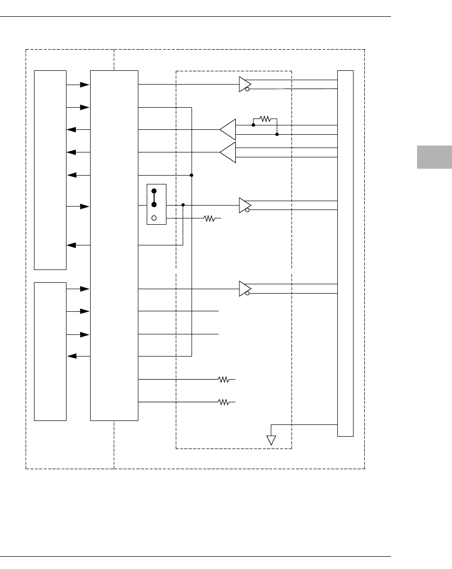
Port Configuration Diagrams
http://www.motorola.com/computer/literature 5-27
5
Figure 5-10. X.21-DCE Port Configuration (Ports 3 and 4)
Z85230 SCC
Z8536 CIO
DB25
X.21 DCE SIM
TXD
RTS_
RXD
CTS_
RTXC
TRXC
DSR_
DTR_
LL_
RL_
DCD_
RI_
TM_
+
-
+
-
RXDB
TXDB
CTRLB
SETB
INDB
GND
RXDA
TXDA
CTRLA
SETA
INDA
J3/MX
17
7
3
2
16
14
24
11
12
17
9
15
+V
+V
+V
NC
NC
2112 971
J8, J9
3
2
1
Transition Module
CPX750HATM
CPX750

5-28 Computer Group Literature Center Web Site
Transition/Bridge Modules
5
Figure 5-11. X.21-DTE Port Configuration (Ports 3 and 4)
Z85230 SCC
Z8536 CIO
DB25
X.21 DTE SIM
TXD
RTS_
RXD
CTS_
RTXC
TRXC
DSR_
DTR_
LL_
RL_
DCD_
RI_
TM_
+
-
+
-
TXDB
RXDB
INDB
SETB
GND
TXDA
RXDA
INDLA
SETA
J3/MX
7
2
3
14
16
17
9
12
+V
+V
NC
NC
Transition Module
J8, J9
3
2
1
CPX750HATM
CPX750
CTRLB
CTRLA
+
-
NC
11
24
15

CPV5350TM80 Transition Module
http://www.motorola.com/computer/literature 5-29
5
CPV5350TM80 Transition Module
The CPV5350TM80 transition module provides rear I/O connectivity for
the CPV5350 CPU controller module.
The CPV5350TM80 provides rear panel connections for:
❏Two Ethernet ports
❏Two serial ports
❏Two Universal Serial Bus ports
❏One parallel port
❏One video port
❏One keyboard/mouse port
❏On-board headers for keyboard/mouse/power LED
❏On-board headers for a speaker and reset
❏On-board EIDE header (supports up to four devices), floppy
drives,
When the identical function is available through the CPV5350 controller’s
front panel and the CPV5350TM80 transition module’s panel, you can use
either the front or the rear connector, but not both.
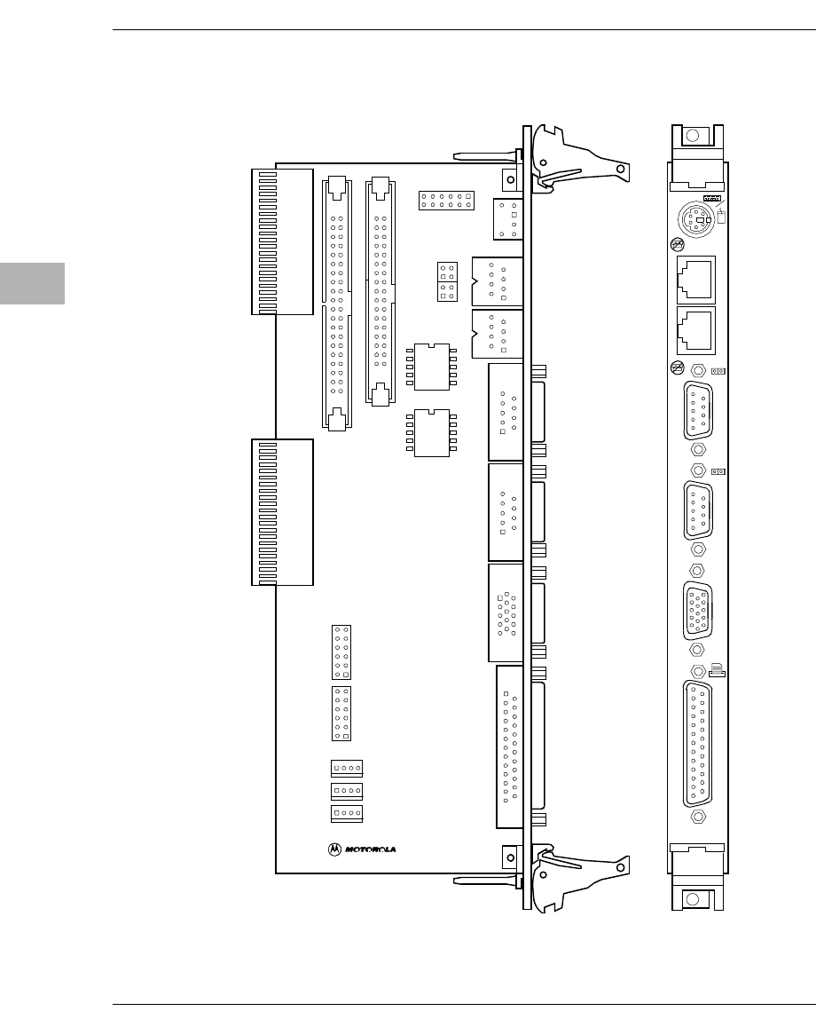
5-30 Computer Group Literature Center Web Site
Transition/Bridge Modules
5
The next figure shows the CPV5350TM80 front panel and on-board
connectors and jumpers.
2493 9902
BTI
GND
GND
INTRUDER
BYPASS
VCC
GND
SMDATA
SMALT
GND
VCC
SMCLK
GND
VCC
VCC
VCC
VCC
VCC
PBRRESET
SIDE
ALARM
SPKR
SCSI
PIDE
J2
J1
J3
J4
J7
J20
J16
J10
J21
J18
J13
J19
J12
J5
J9
KBDCLK
GND
KVCC
MCLK
KBDDAT
MDAT
PWR
GND
GND
GND
J6
T2
T1
CPV5350TM
V
I
D
E
O
E
T
H
E
R
N
E
T
1
2
2
1
P
A
R
A
L
L
E
L
J14

Connectors
http://www.motorola.com/computer/literature 5-31
5
Connectors
The following table lists the connectors available to support devices on the
CPV5350. The figure on the preceding page shows the location of the
connectors described in the table.
Connector Description
J1 SM Bus and LM78 connector
J2 EIDE indicator lights, push-button reset, alarm indicator,
and speaker connector
J3 Fan tachometer connector
J4 Fan tachometer connector
J5 EIDE connector
J6 Keyboard/Mouse, power LED connector
J7 Miscellaneous Power
J9 Floppy Connector
J10 COM 2
J12 USB port
J13 Ethernet 1
J14 Keyboard/Mouse
J16 Video Connector
J18 Ethernet 2
J19 USB Port
J20 Parallel port connector
J21 COM1
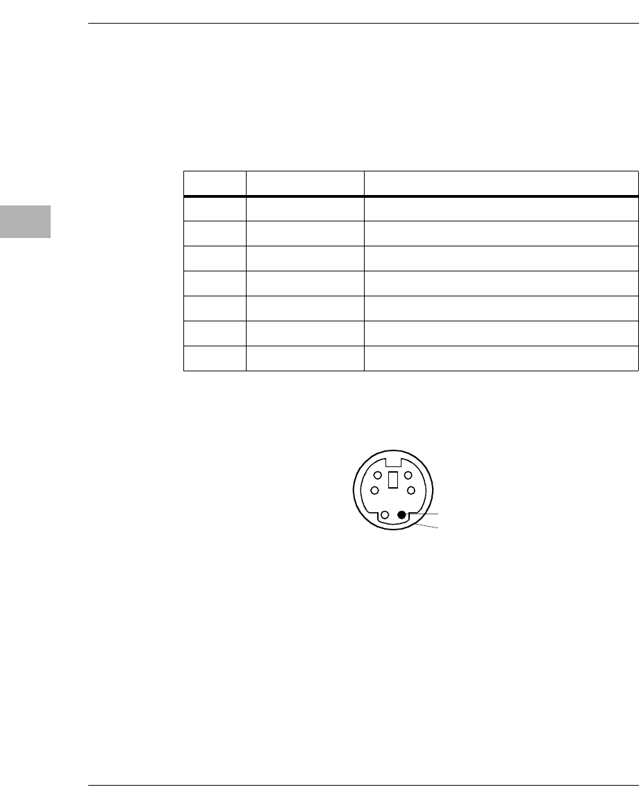
5-32 Computer Group Literature Center Web Site
Transition/Bridge Modules
5
Keyboard/Mouse PS2 Connector
The keyboard/mouse connector (J14) uses a 6-pin, female PS/2 connector.
Figure 5-12. Keyboard/Mouse Connector Diagram
Table 5-15. Keyboard/Mouse P/S2 Connector Pin
Assignments (J14)
Pin Signal Mnemonic Signal Description
1 KBDDAT Keyboard Data
2 AUXDAT Auxiliary Data
3 GND Ground
4 KBDVCC Keyboard Power (current limited to .75 Amp)
5 KBDCLK Keyboard Clock
6 AUXCLK Auxiliary Clock
7 CGND Common Ground
2489 9902
6
4
2
5
3
1
7
Connectors
http://www.motorola.com/computer/literature 5-33
5
Ethernet Connectors
Ethernet 1 (J13) and Ethernet 2 (J18) use standard RJ-45 connectors.
Serial Port Connectors
COM 1 (Serial Port 1, J21) and COM 2 (Serial Port 2, J10) use 2 x 9-pin
D-sub connectors.
Table 5-16. Ethernet Connector Pin Assignments (J13 and
J18)
Pin Signal Mnemonic Signal Description
1 TX+ Differential transmit lines
2 TX- Differential transmit lines
3 RX+ Differential receive lines
4-- --
5-- --
6 RX- Differential receive lines
7-- --
8-- --
Table 5-17. Serial Port Connector Pin Assignments
(J21 and J10)
Pin Signal
Mnemonic Signal Description
1 DCD- Data set has detected the data carrier
2 RX Receives serial data input from communication link
3 TX Sends serial output to communication link
4 DTR- Data set is ready to establish a communication link
5 GND Ground
5-34 Computer Group Literature Center Web Site
Transition/Bridge Modules
5
Video Connector
The video connector (J16) uses a 15-pin high density D-sub connector.
6 DSR- Data set is ready to establish a communication link
7 RTS- Indicates to data set that UART is ready to exchange data
8 CTS- Data set is ready to exchange data
9 RI- Modem has received a telephone ringing signal
Table 5-17. Serial Port Connector Pin Assignments
(J21 and J10) (continued)
Pin Signal
Mnemonic Signal Description
Table 5-18. Video Connector Pin Assignments (J16)
Pin Signal
Mnemonic Signal Description
1 RED Red signal
2 GREEN Green signal
3 BLUE Blue signal
4 NC Not connected
5 DACVSS Video return
6 DACVSS Video return
7 DACVSS Video return
8 DACVSS Video return
9 NC Not connected
10 DACVSS Video return
11 NC Not connected
Connectors
http://www.motorola.com/computer/literature 5-35
5
Parallel Port Connector (J20)
The parallel port (J20) uses a 25-pin, D-sub connector.
12 DDCDAT Display data channel data signal for DDC2 support
13 HSYNC Horizontal synchronization
14 VSYNC Vertical synchronization
15 DDCCLK Display data channel clock signal for DDC2 support
Table 5-18. Video Connector Pin Assignments (J16)
Pin Signal
Mnemonic Signal Description
Table 5-19. Parallel Connector Pin Assignments (J20)
Pin Signal Mnemonic Signal Description
1 STROBE- Data at parallel port is valid
2 D0 Parallel data lines
3 D1 Parallel data line
4 D2 Parallel data line
5 D3 Parallel data line
6 D4 Parallel data line
7 D5 Parallel data line
8 D6 Parallel data line
9 D7 Parallel data line
10 ACK- Acknowledge data retrieval
11 BUSY Printer cannot accept more data
12 PE Printer out of paper
13 SELECT Set high when selected
14 AFD- Causes printer to add a line feed
5-36 Computer Group Literature Center Web Site
Transition/Bridge Modules
5
EIDE Headers (J5)
15 ERR- Set low when an error is detected
16 INIT- Initializes the printer
17 SLIN- Selects the printer
18 GND Ground
19 GND Ground
20 GND Ground
21 GND Ground
22 GND Ground
23 GND Ground
24 GND Ground
25 GND Ground
Table 5-19. Parallel Connector Pin Assignments (J20)
Pin Signal Mnemonic Signal Description
Table 5-20. EIDE Header (J5) Pin Assignments
Pin Signal
Mnemonic Signal
Description Pin Signal
Mnemonic Signal
Description
1 Reset Reset signal
to drive
2 GND Ground
3 DD7 Drive data
line
4 DD8 Drive data
line
5 DD6 Drive data
line
6 DD9 Drive data
line
7 DD5 Drive data
line
8 DD10 Drive data
line
Connectors
http://www.motorola.com/computer/literature 5-37
5
9 DD4 Drive data
line
10 DD11 Drive data
line
11 DD3 Drive data
line
12 DD12 Drive data
line
13 DD2 Drive data
line
14 DD13 Drive data
line
15 DD1 Drive data
line
16 DD14 Drive data
line
17 DD0 Drive data
line
18 DD15 Drive data
line
19 GND Ground 20 - -
21 DMARQ Drive DMA
request
22 GND Ground
23 IOW Drive I/O
write
24 GND Ground
25 IOR Drive I/O
read
26 GND Ground
27 IORDY Drive is ready
for I/O cycles
28 CSEL Cable select
29 DMACK Drive DMA
acknowledge
30 GND Ground
31 INTRQ Drive
interrupt
request
32 IOCS16 16 bit
register is
decoded
Table 5-20. EIDE Header (J5) Pin Assignments
Pin Signal
Mnemonic Signal
Description Pin Signal
Mnemonic Signal
Description

5-38 Computer Group Literature Center Web Site
Transition/Bridge Modules
5
Floppy Header (J9)
33 DA1 Drive register
and data port
address lines
34 PDIAG Output from
drive 1 and
monitored
by drive 0
35 DA0 Drive register
and data port
address lines
36 DA2 Drive
register and
data port
address lines
37 CS1 Chip select
drive 0, also
command
register block
select
38 CS3 Chip select
drive 1, also
command
register
block select
39 DASP Drive active
slave present
40 GND Ground
Table 5-20. EIDE Header (J5) Pin Assignments
Pin Signal
Mnemonic Signal
Description Pin Signal
Mnemonic Signal
Description
Table 5-21. Floppy Header (J9) Pin Assignments
Pin Signal
Mnemonic Signal
Description Pin Signal
Mnemonic Signal
Description
1 GND Drive
common
2 DRVDENS0 Disk density
select
communication
3- - 4- -
5 GND Drive
common
6 DRVDENS1 Disk density
select
communication
7 GND Drive
common
8 INDEX Beginning of a
track
Connectors
http://www.motorola.com/computer/literature 5-39
5
9 GND Drive
common
10 MTR0 Motor enable
output
11 GND Drive
common
12 DS1 Drive select 1
13 GND Drive
common
14 DS0 Drive select 0
15 GND Drive
common
16 MTR1 Motor enable
output
17 GND Drive
common
18 DIR Controls
direction of the
floppy disk drive
head during seek
operation
19 GND Drive
common
20 STEP Supplies step
pulses to move
head during seek
operations
21 GND Drive
common
22 WDATA Writes serial data
to disk drive
23 GND Drive
common
24 WGATE Enables head of
disk drive to
write to disk
25 GND Drive
common
26 TR0 Head of floppy
disk drive is at
track 0
Table 5-21. Floppy Header (J9) Pin Assignments
Pin Signal
Mnemonic Signal
Description Pin Signal
Mnemonic Signal
Description
5-40 Computer Group Literature Center Web Site
Transition/Bridge Modules
5
Keyboard/Mouse/Power LED Header (J6)
The table below shows the pin assignments for the keyboard, mouse, and
power LED header.
27 GND Drive
common
28 WPROT Disk is write
protected
29 GND Drive
common
30 RDATA Raw read data
from disk drive
31 GND Drive
common
32 HDSEL Determines the
side of the floppy
disk being
accessed
33 GND Drive
common
34 DSKCHG Notifies disk
drive controller
that the drive
door is open
Table 5-21. Floppy Header (J9) Pin Assignments
Pin Signal
Mnemonic Signal
Description Pin Signal
Mnemonic Signal
Description
Table 5-22. Keyboard/Mouse/Power LED Header (J6) Pin
Assignments
Pin Signal
Mnemonic Signal
Description Pin Signal
Mnemonic Signal
Description
1PWRLEDPower LED
Indicator
2 KBDCLK Clock for
keyboard
3 GND Ground 4 KBDDAT Data line for
keyboard
Connectors
http://www.motorola.com/computer/literature 5-41
5
USB Headers (J12 and J19)
5 GND Ground 6 AUXDAT Data line for
mouse
7- - 8GND Ground
9 GND Ground 10 KBDVCC Keyboard
power (.75A)
11 - - 12 AUXCLK Clock for
mouse
Table 5-22. Keyboard/Mouse/Power LED Header (J6) Pin
Assignments (continued)
Pin Signal
Mnemonic Signal
Description Pin Signal
Mnemonic Signal
Description
Table 5-23. USB Headers (J12 and J19) Pin Assignments
Pin Signal Mnemonic Signal Description
1 +5V Current limited USB power
2 DATA- USB serial communications differential pair
3 DATA+ USB serial communications differential pair
4 GND USB Port common
5-42 Computer Group Literature Center Web Site
Transition/Bridge Modules
5
SM Bus and LM78 Header (J1)
Table 5-24. SM Bus and LM78 Header (J1)Pin
Assignments
Pin Signal
Mnemonic Signal
Description Pin Signal
Mnemonic Signal
Description
1OPEN- Chassis
intrusion
signal
2 GND Ground
3 GND Ground 4 SMBALERT- SM bus
interrupt
signal
5 GND Ground 6 SMBDATA SM bus data
strobe signal
7VCC SM bus
power
8 SMBCLK SM bus
clock signal
9 BYPASS Power
switch
bypass signal
10 VCC SM bus
power
11 BT1- Board
temperature
interrupt
signal
12 GND Ground
Connectors
http://www.motorola.com/computer/literature 5-43
5
Fan Tachometer Headers (J3 and J4)
Refer to the next table for pin assignments and signal descriptions for the
Fan Tachometer headers (J3 and J4) on the CPV5350 Transition Module.
Indicator LED/Miscellaneous Header (J2)
Table 5-25. Fan Tachometer Header (J3 and J4) Pin
Assignments
Pin Signal Mnemonic Signal Description
1 VCC SM bus power
2 TACH Tachometer input for fan
3 GND Ground
4 +12V 12 volt power
Table 5-26. Indicator LED/Miscellaneous Header (J2) Pin
Assignments
Pin Signal
Mnemonic Signal Description Pin Signal
Mnemonic Signal
Description
1 VCC +5V power (limited
to .75A total)
2 SPEAKER Speaker
output
3 VCC +5V power (limited
to .75A total)
4ALARMAlarm
indicator
LED
5-44 Computer Group Literature Center Web Site
Transition/Bridge Modules
5
5 VCC +5V power (limited
to .75A total)
6 EIDE_LED Secondary
channel
EIDE
activity LED
7 VCC +5V power (limited
to .75A total)
8- -
9 VCC +5V power (limited
to .75A total)
10 - -
11 GND Ground 12 PBRESET- Push button
reset
Table 5-26. Indicator LED/Miscellaneous Header (J2) Pin
Assignments (continued)
Pin Signal
Mnemonic Signal Description Pin Signal
Mnemonic Signal
Description
6-1
6
6Subassembly Reference
Chapter Overview
This chapter provides reference information for the various subassemblies
of the CPX8216 and CPX8216T system. It covers only those items
associated with the system enclosure. For information about CompactPCI
board components, refer to the appropriate chapter in this manual.
The following table lists the system components covered in this chapter:
Table 6-1. System Components
Topic: Page:
Parts of the System 6-2
CompactPCI Card Cage Reference 6-4
Backplane Reference 6-5
Alarm Display Panel 6-51
Power Distribution Panel 6-54
Power Supplies 6-58
6-2 Computer Group Literature Center Web Site
Subassembly Reference
6
Parts of the System
Figure 6-1. CPX8216 Front View
12345678910 11 12 13 14 15 16
MI NOR MAJOR CRI TI CA L
TELCO
SYSTEM COMPONENT
SYSTEM IN SERVICE OUT OF SER VICE ALARM
CONNECTIONSTATUS
STATUS
12
43
ESD BONDING
POINT
TBD
1
IN OUT OF
SERVICE
SERVICE
2
IN OUT OF
SERVICE
SERVICE
3
IN OUT OF
SERVICE
SERVICE
123456789101112 13 14 15 16
Alarm Board Front Peripheral Bay
Power Supplies
Cable
Pass-Thru
CompactPCI
Cardcage
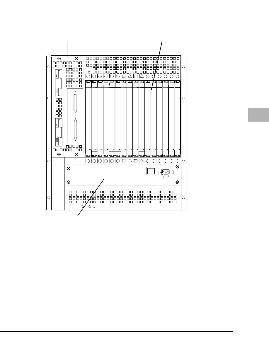
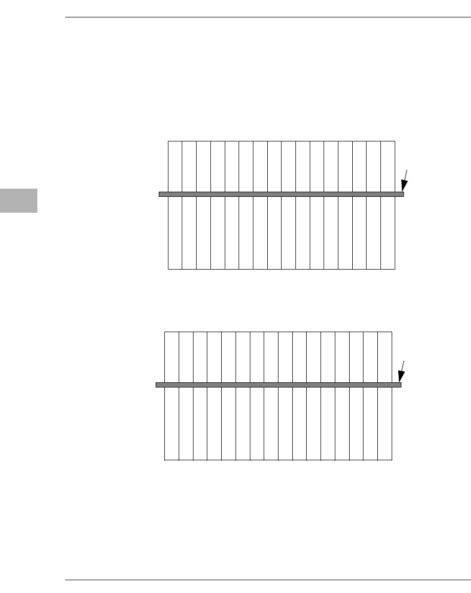
6-4 Computer Group Literature Center Web Site
Subassembly Reference
6
CompactPCI Card Cage Reference
Industry standard CompactPCI cardguides are used for the front controller
boards and rear transition boards. The CPU slot is identified with red guide
rails, the I/O slots with black rails, and the Hot Swap Controller/Bridge
slots with tan rails (see Figure 6-3 and Figure 6-4 on page 6-4).
Figure 6-3. Card Cage Rail Color Scheme—CPX8216 Standard System
Figure 6-4. Card Cage Rail Color Scheme—CPX8216T H.110 System
Each slot, both controller and transition, has one ESD cardguide clip and
one ESD alignment pin clip. All clips are located on the bottom cardguide
only.
I/O Slot (Black)
CPU (Red)
None
123
4
5
678910 11 12 13 14 15 16
Bridge (Tan)
None
I/O Slot (Black)
I/O Slot (Black)
I/O Slot (Black)
I/O Slot (Black)
I/O Slot (Black)
I/O Slot (Black)
I/O Slot (Black)
I/O Slot (Black)
I/O Slot (Black)
I/O Slot (Black)
I/O Slot (Black)
I/O Trns (Black)
I/O Trns (Black)
I/O Trns (Black)
I/O Trns (Black)
I/O Trns (Black)
I/O Trns (Black)
I/O Trns (Black)
I/O Trns (Black)
I/O Trns (Black)
I/O Trns (Black)
I/O Trns (Black)
I/O Trns (Black)
CPU (Red) CPU Trns (Red)
CPU Trns (Red)
Bridge (Tan)
Front Slots
Rear Slots
Backplane
I/O Slot (Black)
CPU (Red)
H.110 Bridge (Tan)
123
4
5
678910 11 12 13 14 15 16
I/O Slot (Black)
I/O Slot (Black)
I/O Slot (Black)
I/O Slot (Black)
I/O Slot (Black)
I/O Slot (Black)
I/O Slot (Black)
I/O Slot (Black)
I/O Slot (Black)
I/O Slot (Black)
I/O Slot (Black)
I/O Trns (Black)
I/O Trns (Black)
I/O Trns (Black)
I/O Trns (Black)
I/O Trns (Black)
I/O Trns (Black)
I/O Trns (Black)
I/O Trns (Black)
I/O Trns (Black)
I/O Trns (Black)
I/O Trns (Black)
I/O Trns (Black)
CPU (Red) CPU Trns (Red)
CPU Trns (Red)
None
Front Slots
Rear Slots
Backplane
None
H.110 Bridge (Tan)
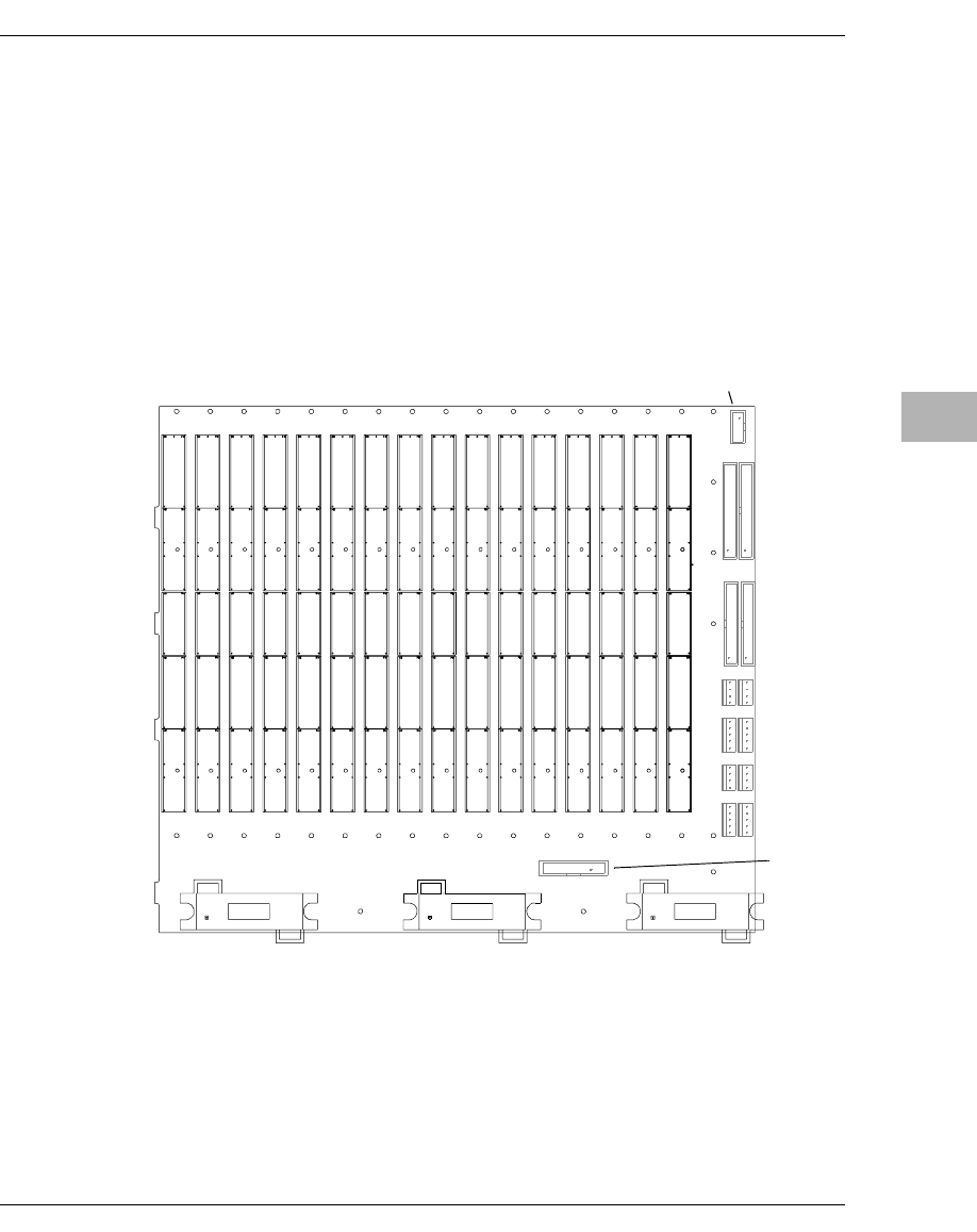
Backplane Reference
http://www.motorola.com/computer/literature 6-5
6
Backplane Reference
The backplane provides the interconnect for all 16-slot, 6U CompactPCI
bus, N+1 power distribution, alarm signal distribution, and IDE device
signal/status distribution.
All sixteen CompactPCI slots accept any standard 6U CompactPCI board
or transition module which meet IEEE 1101.1, IEEE 1101.10, and
IEEE1101.11 specifications. The slots are 64-bit, 33 MHz PCI compliant.
Figure 6-5. CPX8216 and CPX8216T Backplane—Primary Side
P1
P2
P3
P4
P5
PRIMARY SIDE
FDA
IDEA
PWR1
PWR4
PWR2
FDB
IDEB
PWR3 SIG1
SIG2
SIG3
SIG4
PS1 PS2 PS3
ALARM
Secondary Side
Alarm, Floppy, IDE
PWR, and SIG Connectors
H.110 BAT
and Ring
Voltages on
Secondary
Side
(CPX8216T
Only)
6-6 Computer Group Literature Center Web Site
Subassembly Reference
6
Power Supply Connectors (PS1, PS2, PS3)
The three power supply connectors, PS1, PS2, and PS3, are located on the
primary side of the backplane.
Note The shaded pins are high current pins. Present[n]# is grounded
on the backplane.
Table 6-2. PS1, PS2, and PS3 Pin Assignments
Pin Signal Signal Pin
1GND Present[n]# 16
2GND -12Vdc 17
3+3.3Vdc A_DOUT# 18
4+3.3Vdc PS[n]_DIN# 19
5 +S5Vdc -12Vdc 20
6-S5Vdc N/C 21
7+5_Share N/C 22
8+S3.3Vdc N/C 23
9-S3.3Vdc N/C 24
10 +3.3_Share N/C 25
11 +12Vdc +5Vdc 26
12 +12Vdc +5Vdc 27
13 +12Vdc GND 28
14 A_CLK GND 29
15 PS[n]_FRAME#
H.110 Power Connector (CPX8216T Only)
http://www.motorola.com/computer/literature 6-7
6
H.110 Power Connector (CPX8216T Only)
H.110 BAT and Ring voltages are supplied to the backplane directly from
the Power Distribution Panel. This section applies to CPX8216T systems
only.
Table 6-3. Fan Module Pin Assignments
Pin Signal Color Pin Signal Color
1N/C 6N/C
2 +12V_System In Grey 7 +12V_System Out Brown
3 +12V_Fan Red 8 +12V_Fan_Rtn Black
4 Tach Blue 9 Speed Ctl Yellow
5N/C 10N/C
Table 6-4. H.110 Power Connector
Pin Signal
1-Vbat
2Vbat RTN
3-SELVbat
4SELVbat RTN
5VRG
6VRG RTN

6-8 Computer Group Literature Center Web Site
Subassembly Reference
6
Alarm Interface Connector (ALARM)
The alarm interface connector is located on the secondary side of the
backplane. Alarm signals are routed through the backplane to the ALARM
connector. The alarm board attaches to this connector by ribbon cable.
Floppy Drive Connectors (FDA, FDB)
The backplane supports two standard IDE floppy drives. The floppy drive
connectors, FDA and FDB, are located on the secondary side of the
backplane. FDA is controlled by domain A, and FDB is controlled by
domain B.
Table 6-5. ALARM Connector Pin Assignments
Pin Signal Pin Signal
1 ALM_A_CLK 2 GND
3 ALM_B_CLK 4 GND
5 ALM_A_DOUT# 6 ALM_A_5V
7 ALM_B_DOUT# 8 ALM_B_5V
9 ALM_A_FRAME# 10 ALM_B_FRAME#
11 ALM_A_DIN# 12
Table 6-6. FDA and FDB Pin Assignments
Pin Signal Signal Pin
1 GND Not Connected 2
3 GND Not Connected 4
5 Key (pin missing) Not Connected 6
7 GND F_[n]_INDEX# 8
9 GND F_[n]_MTRO# 10
11 GND F_[n]_DS1# 12
IDE Drive Connectors (IDEA and IDEB)
http://www.motorola.com/computer/literature 6-9
6
IDE Drive Connectors (IDEA and IDEB)
The two IDE drive connectors are located on the secondary side of the
backplane. IDEA is controlled by Domain A; IDEB by Domain B.
13 GND F_[n]_DS0# 14
15 GND F_[n]_MTR1# 16
17 GND F_[n]_DIR# 18
19 GND F_[n]_STEP# 20
21 GND F_[n]_WDATA# 22
23 GND F_[n]_WGATE# 24
25 GND F_[n]_TR0# 26
27 GND F_[n]_WPROT# 28
29 GND F_[n]_RDATA# 30
31 GND F_[n]_HDSEL# 32
33 GND F_[n]_DSKCHG# 34
Table 6-6. FDA and FDB Pin Assignments (continued)
Pin Signal Signal Pin
Table 6-7. IDEA and IDEB Pin Assignments
Pin Signal Signal Pin
1 IDE_[n]_RST# GND 2
3 IDE_[n]_D7 IDE_[n]_D8 4
5 IDE_[n]_D6 IDE_[n]_D9 6
7 IDE_[n]_D5 IDE_[n]_D10 8
9 IDE_[n]_D4 IDE_[n]_D11 10
11 IDE_[n]_D3 IDE_[n]_D12 12
13 IDE_[n]_D2 IDE_[n]_D13 14
6-10 Computer Group Literature Center Web Site
Subassembly Reference
6
Peripheral Power Connectors (PWR1, PWR2,
PWR3, PWR4)
The four peripheral power connectors are located on the secondary side of
the CPX8216 backplane. All four connectors have the same pin-out and
can be used interchangeably.
15 IDE_[n]_D1 IDE_[n]_D13 16
17 IDE_[n]_D0 IDE_[n]_D15 18
19 GND Key (pin missing) 20
21 IDE_[n]_DMARQ GND 22
23 IDE_[n]_DIOW# GND 24
25 IDE_[n]_DIOR# GND 26
27 IDE_[n]_IORDY No Connect 28
29 IDE_[n]_DMACK# GND 30
31 IDE_[n]_INTRQ IDE_[n]_IOCS16# 32
33 IDE_[n]_DA1 IDE_[n]_PDIAG# 34
35 IDE_[n]_DA0 IDE_[n]_DA2 36
37 IDE_[n]_CS1FX# IDE_[n]_CS3FX# 38
39 IDE_[n]_DASP GND 40
Table 6-7. IDEA and IDEB Pin Assignments (continued)
Pin Signal Signal Pin
Table 6-8. PWR1, PWR2, PWR3, PWR4 Pin Assignments
Pin Signal
1+5 Volts
2 Ground
Peripheral Signal Connectors (SIG1, SIG2, SIG3, SIG4)
http://www.motorola.com/computer/literature 6-11
6
Peripheral Signal Connectors (SIG1, SIG2,
SIG3, SIG4)
The four peripheral signal connectors are located on the secondary side of
the CPX8216 backplane. All four connectors have the same pin-out. The
connectors map to different locations in the Hot Swap Controller
peripheral registers, and cannot be used interchangeably.
CompactPCI Connectors (P1, P2, P3, P4, P5)—
CPX8216 Standard Backplane
Primary (Front) Side I/O Connectors (Slots 1-6 and 11-16)
In the front I/O slots (system slots 1-6 and 11-16), connectors P3, P4, and
P5 are reserved for user I/O.
3 Ground
4 +12 Volts
Table 6-8. PWR1, PWR2, PWR3, PWR4 Pin Assignments
Pin Signal
Table 6-9. SIG1, SIG2, SIG3, SIG4 Pin Assignments
Pin Signal
1 Per[n]_Pwr_ON#
2Per[n]_LED1#
3Per[n]_LED2#
4 Per[n]_PSNT_A#
5 Per[n]_PSNT_B#
6-12 Computer Group Literature Center Web Site
Subassembly Reference
6
Connectors P1 and P2 carry the CompactPCI bus (bus A for slots 1-6, bus
B for slots 11-16).
Table 6-10. P5 Connector, I/O Slots 1-6 and 11-16
(User I/O)
POS Row Z Row A Row B Row C Row D Row E Row F
22-1 GND I/O I/O I/O I/O I/O GND
All I/O pins pass through the backplane to the transition module, they do not make any connection
to the backplane.
Table 6-11. P4 Connector, I/O Slots 1-6 and 11-16 (User I/O)
POS Row Z Row A Row B Row C Row D Row E Row F
25-15 GND I/O I/O I/O I/O I/O GND
14
KEY AREA
13
12
11-1 GND I/O I/O I/O I/O I/O GND
All I/O pins pass through the backplane to the transition module, they do not make any connection
to the backplane.
Table 6-12. P3 Connector, I/O Slots 1-6 and 11-16 (User I/O)
POS Row Z Row A Row B Row C Row D Row E Row F
19-1 GND I/O I/O I/O I/O I/O GND
All I/O pins pass through the backplane to the transition module, they do not make any connection
to the backplane.
Primary (Front) Side I/O Connectors (Slots 1-6 and 11-16)
http://www.motorola.com/computer/literature 6-13
6
Table 6-13. P2 Connector, I/O Slots 1-6 and 11-16 (CPCI Bus)
POS Row
Z Row A Row B Row C Row D Row E Row
F
22 GND GA4 GA3 GA2 GA1 GA0 GND
21 GND GND RSV RSV RSV GND
20 GND GND RSV GND RSV GND
19 GND GND GND RSV RSV RSV GND
18 GND _BRSVP2
A18
_BRSVP2B
18
_BRSVP2
C18
GND _BRSVP2E18 GND
17 GND _BRSVP2
A17
GND GND
16 GND _BRSVP2
A16
_BRSVP2B
16
_BRSVP2E16 GND
15 GND _BRSVP2
A15
GND GND
14 GND _AD[35] _AD[34] _AD[33] GND _AD[32] GND
13 GND _AD[38] GND VIO _AD[37] _AD[36] GND
12 GND _AD[42] _AD[41] _AD[40] GND _AD[39] GND
11 GND _AD[45] GND VIO _AD[44] _AD[43] GND
10 GND _AD[49] _AD[48] _AD[47] GND _AD[46] GND
9 GND _AD[52] GND VIO _AD[51] _AD[50] GND
8 GND _AD[56] _AD[55] _AD[54] GND _AD[53] GND
7 GND _AD[59] GND VIO _AD[58] _AD[57] GND
Signals beginning with an underscore (_) are prefixed with the bus name:
*For boards located in slots 1-6 (Domain A), the signal name is prefixed with PCI_A (for
example, PCI_A_AD[49]).
*For boards located in slots 11-16 (Domain B), the signal name is prefixed with PCI_B (for
example, PCI_B_AD[49]).
Signals RSV are not connected.
Signals beginning with _BRSV are bussed, but not used.
6-14 Computer Group Literature Center Web Site
Subassembly Reference
6
6 GND _AD[63] _AD[62] _AD[61] GND _AD[60] GND
5 GND _C/BE[5]# GND VIO C/BE[4]# _PAR64 GND
4 GND VIO _BRSVP2B
4
_C/BE[7]# GND _C/BE[6] GND
3 GND GND GND
2 GND GND
1 GND GND GND
Table 6-14. P1 Connector, I/O Slots 1-6 and 11-16 (CPCI Bus)
POS Row
Z Row A Row B Row C Row D Row E Row
F
25 GND 5V _REQ64# A_ENUM# 3.3V 5V GND
24 GND _AD[1] 5V VIO _AD[0] _ACK64# GND
Signals beginning with an underscore (_) are prefixed with the bus name:
*For boards located in slots 1-6 (Domain A), the signal name is prefixed with PCI_A (for
example, PCI_A_AD[49]).
*For boards located in slots 11-16 (Domain B), the signal name is prefixed with PCI_B (for
example, PCI_B_AD[49]).
Signals RSV are not connected.
Signals beginning with _BRSV are bussed, but not used.
Signal A_ENUM# in Domain A (slots 1-6), B_ENUM# in Domain B (Slots 11-16).
Table 6-13. P2 Connector, I/O Slots 1-6 and 11-16 (CPCI Bus)
POS Row
Z Row A Row B Row C Row D Row E Row
F
Signals beginning with an underscore (_) are prefixed with the bus name:
*For boards located in slots 1-6 (Domain A), the signal name is prefixed with PCI_A (for
example, PCI_A_AD[49]).
*For boards located in slots 11-16 (Domain B), the signal name is prefixed with PCI_B (for
example, PCI_B_AD[49]).
Signals RSV are not connected.
Signals beginning with _BRSV are bussed, but not used.
Primary (Front) Side I/O Connectors (Slots 1-6 and 11-16)
http://www.motorola.com/computer/literature 6-15
6
23 GND 3.3V _AD[4] _AD[3] 5V _AD[2] GND
22 GND _AD[7] GND 3.3V _AD[6] _AD[5] GND
21 GND 3.3V _AD[9] _AD[8] _M66EN _C/BE[0]# GND
20 GND _AD[12] GND VIO _AD[11] _AD[10] GND
19 GND 3.3V _AD[15] _AD[14] GND _AD[13] GND
18 GND _SERR# GND 3.3V _PAR _C/BE[1] GND
17 GND 3.3V _SDONE _SBO# GND _PERR# GND
16 GND _DEVSEL# GND VIO _STOP# _LOCK# GND
15 GND 3.3V _FRAME# _IRDY# BD_SEL[n]# _TRDY# GND
14-
12 KEY AREA
11 GND _AD[18} _AD[17] _AD[16] GND _C/BE[2]# GND
10 GND _AD[21] GND 3.3V _AD[20] _AD[19] GND
9 GND _C/BE[3] _IDSEL _AD[23] GND _AD[22] GND
8 GND _AD[26] GND VIO _AD[25] _AD[24] GND
7 GND _AD[30] _AD[29] _AD[28] GND _AD[27] GND
6 GND REQ[N]# GND 3.3V CLK[N] _AD[31] GND
5 GND _BRSVP1A
5
_BRSVP1B
5
RST[N]# GND GNT[N]# GND
Table 6-14. P1 Connector, I/O Slots 1-6 and 11-16 (CPCI Bus)
POS Row
Z Row A Row B Row C Row D Row E Row
F
Signals beginning with an underscore (_) are prefixed with the bus name:
*For boards located in slots 1-6 (Domain A), the signal name is prefixed with PCI_A (for
example, PCI_A_AD[49]).
*For boards located in slots 11-16 (Domain B), the signal name is prefixed with PCI_B (for
example, PCI_B_AD[49]).
Signals RSV are not connected.
Signals beginning with _BRSV are bussed, but not used.
Signal A_ENUM# in Domain A (slots 1-6), B_ENUM# in Domain B (Slots 11-16).
6-16 Computer Group Literature Center Web Site
Subassembly Reference
6
4 GND _BRSVP1A
4
HLTY[N]# VIO _INTP _INTS GND
3 GND _INTA# _INTB# _INTC# 5V _INTD# GND
2 GND TCK 5V TMS TDO TDI GND
1 GND 5V -12V TRST# +12V 5V GND
Table 6-14. P1 Connector, I/O Slots 1-6 and 11-16 (CPCI Bus)
POS Row
Z Row A Row B Row C Row D Row E Row
F
Signals beginning with an underscore (_) are prefixed with the bus name:
*For boards located in slots 1-6 (Domain A), the signal name is prefixed with PCI_A (for
example, PCI_A_AD[49]).
*For boards located in slots 11-16 (Domain B), the signal name is prefixed with PCI_B (for
example, PCI_B_AD[49]).
Signals RSV are not connected.
Signals beginning with _BRSV are bussed, but not used.
Signal A_ENUM# in Domain A (slots 1-6), B_ENUM# in Domain B (Slots 11-16).
Primary (Front) Side CPU Slot Connectors (7 and 9)
http://www.motorola.com/computer/literature 6-17
6
Primary (Front) Side CPU Slot Connectors (7 and 9)
Table 6-15. P5 Connector, CPU Slots 7 and 9
POS Row
Z Row A Row B Row C Row D Row E Row
F
22 GND I/O I/O I/O I/O I/O GND
21 GND I/O I/O I/O I/O I/O GND
20 GND I/O I/O I/O I/O I/O GND
19 GND I/O I/O I/O I/O I/O GND
18 GND I/O I/O I/O I/O I/O GND
17 GND I/O I/O I/O I/O I/O GND
16 GND I/O I/O I/O I/O I/O GND
15 GND I/O I/O I/O I/O I/O GND
14 GND I/O I/O I/O I/O I/O GND
13 GND I/O I/O I/O I/O I/O GND
12 GND I/O I/O I/O I/O I/O GND
11 GND I/O I/O I/O I/O I/O GND
10 GND _TR0# _WPROT# _RDATA# _HDSEL# _DSKCHG
#
GND
9 GND _MTR1# _DIR# _STEP# _WDATA# _WGATE# GND
8 GND _RSV1# _INDEX# _MTR0# _DS1# A_DS0# GND
7 GND _CS1FX# _CS3FX# _DA1 _DASP#_RSV0# GND
Signals in bold text are prefixed with IDE_A if the board resides in slot 7 or IDE_B if the board
resides in slot 9.
Signals in shaded cells are prefixed with F_A if the board resides in slot 7 or F_B if the board
resides in slot 9.
All I/O pins pass through the backplane to the transition module; they do not make any connection
to the backplane.
6-18 Computer Group Literature Center Web Site
Subassembly Reference
6
6 GND _IOCS16# I/O _PDIAG# _DA0 _DA2 GND
5GND_DMARQ _IORDY _DIOW# _DMACK# _DIOR# GND
4GND_D14 _D0 I/O _D15 _INTRQ GND
3GND_D3 _D12 _D2 _D13 _D1 GND
2GND_D9 _D5 _D10 _D4 _D11 GND
1GNDI/O _RST# _D7 _D8 _D6 GND
Table 6-16. P4 Connector, CPU Slots 7 and 9
POS Row Z Row A Row B Row C Row D Row E Row F
25 GND _AD36 _AD35 _AD34 _AD33 _AD32 GND
24 GND _AD40 _AD39 _AD38 GND _AD37 GND
23 GND _AD45 _AD44 _AD43 _AD42 _AD41 GND
22 GND _AD49 _+3.3 _AD48 _AD47 _AD46 GND
21 GND _AD53 _AD52 _AD51 GND _AD50 GND
The _+5 and _+3 in the shaded cells are provided by the CPU board; they are not connected to the
system power plane. These signals are prefixed with CPUA if the board resides in slot 7 or CPU
B if the board resides in slot 8 (for example, CPUA_+5).
Signals beginning with an underscore (_) are prefixed with the local PCI bus name:
*For boards located in slot 7 (Domain A), the signal name is prefixed with L_PCI_A (for example,
L_PCI_A_AD17).
*For boards located in slot 9 (Domain B), the signal name is prefixed with L_PCI_B (for example,
L_PCI_B_AD17).
Table 6-15. P5 Connector, CPU Slots 7 and 9 (continued)
POS Row
Z Row A Row B Row C Row D Row E Row
F
Signals in bold text are prefixed with IDE_A if the board resides in slot 7 or IDE_B if the board
resides in slot 9.
Signals in shaded cells are prefixed with F_A if the board resides in slot 7 or F_B if the board
resides in slot 9.
All I/O pins pass through the backplane to the transition module; they do not make any connection
to the backplane.
Primary (Front) Side CPU Slot Connectors (7 and 9)
http://www.motorola.com/computer/literature 6-19
6
20 GND _AD57 _+3.3 _AD56 _AD55 _AD54 GND
19 GND _AD61 _AD60 _AD59 GND _AD58 GND
18 GND _CBE4# _+3.3 _PAR64 _AD63 _AD62 GND
17 GND _REQ64# _CBE7# _CBE6# GND _CBE5# GND
16 GND _AD2 _+3.3 _AD1 _AD0 _ACK64# GND
15 GND _AD6 _AD5 _AD4 GND _AD3 GND
14-
12 KEY AREA
11 GND _AD9 _AD8 _CBE0# GND _AD7 GND
10 GND _AD13 _+5 _AD12 _AD11 _AD10 GND
9 GND _PAR _CBE1# _AD15 GND _AD14 GND
8 GND _STOP# _+5 _LOCK# _PERR# _SERR# GND
7 GND _FRAME# _IRDY# _TRDY# GND _DEVSEL
#
GND
6 GND _AD18 _+5 _AD17 _AD16 CBE2# GND
5 GND _AD21 _CLK _AD20 GND _AD19 GND
4 GND _CBE3# _+5 _IDSEL _AD23 _AD22 GND
3 GND _AD28 _AD27 _AD26 _AD25 _AD24 GND
2 GND _GNT# _REQ# _AD31 _AD30 _AD29 GND
1 GND _INTA# _INTB# _INTC# _INTD# _RST# GND
Table 6-16. P4 Connector, CPU Slots 7 and 9 (continued)
POS Row Z Row A Row B Row C Row D Row E Row F
The _+5 and _+3 in the shaded cells are provided by the CPU board; they are not connected to the
system power plane. These signals are prefixed with CPUA if the board resides in slot 7 or CPU
B if the board resides in slot 8 (for example, CPUA_+5).
Signals beginning with an underscore (_) are prefixed with the local PCI bus name:
*For boards located in slot 7 (Domain A), the signal name is prefixed with L_PCI_A (for example,
L_PCI_A_AD17).
*For boards located in slot 9 (Domain B), the signal name is prefixed with L_PCI_B (for example,
L_PCI_B_AD17).
6-20 Computer Group Literature Center Web Site
Subassembly Reference
6
Table 6-17. P3 Connector, CPU Slots 7 and 9
POS Row Z Row A Row B Row C Row D Row E Row F
19 GND I/O I/O I/O I/O I/O GND
18 GND HS_REQ_ I/O I/O I/O I/O GND
17 GND HS_GNT_ I/O I/O I/O I/O GND
16 GND HS_FLT_ I/O I/O I/O I/O GND
15 GND HS_EJ_ I/O I/O I/O I/O GND
14-1 GND I/O I/O I/O I/O I/O GND
All I/O pins pass through the backplane to the transition module; they do not make any
connection to the backplane.
If the CPU is mounted in slot 7, the HS signals will end with A (for example, HS_REQ_A).
If the CPU is mounted in slot 9, the HS signals will end with B (for example, HS_REQ_B).
Table 6-18. P2 Connector, CPU Slot 7 (Domain A)
POS Row Z Row A Row B Row C Row D Row E Row F
22 GND GA4 GA3 GA2 GA1 GA0 GND
21 GND CLK6 GND RSV RSV RSV GND
20 GND CLK5 GND RSV GND RSV GND
19 GND GND GND RSV RSV RSV GND
18 GND _BRSVP2
A18
_BRSVP2
B18
_BRSVP2
C18
GND _BRSVP2
E18
GND
17 GND _BRSVP2
A17
GND _PRST# _REQ6# GNT6# GND
16 GND _BRSVP2
A16
_BRSVP2
B16
_DEG# GND _BRSVP2
E16
GND
Signals beginning with an underscore (_) are prefixed with the bus name PCI_A (for example,
PCI_A_AD[49]).
Signals RSV are not connected.
Signals beginning with _BRSV are bussed, but not used.
Primary (Front) Side CPU Slot Connectors (7 and 9)
http://www.motorola.com/computer/literature 6-21
6
15 GND _BRSVP2
A15
GND _FAL# REQ5# GNT5# GND
14 GND _AD[35] _AD[34] _AD[33] GND _AD[32] GND
13 GND _AD[38] GND VIO _AD[37] _AD[36] GND
12 GND _AD[42] _AD[41] _AD[40] GND _AD[39] GND
11 GND _AD[45] GND VIO _AD[44] _AD[43] GND
10 GND _AD[49] _AD[48] _AD[47] GND _AD[46] GND
9 GND _AD[52] GND VIO _AD[51] _AD[50] GND
8 GND _AD[56] _AD[55] _AD[54] GND _AD[53] GND
7 GND _AD[59] GND VIO _AD[58] _AD[57] GND
6 GND _AD[63] _AD[62] _AD[61] GND _AD[60] GND
5 GND _C/BE[5]# GND VIO C/BE[4]# _PAR64 GND
4 GND VIO _BRSVP2
B4
_C/BE[7]# GND _C/BE[6] GND
3 GND CLK4 GND GNT3# REQ4# GNT4# GND
2 GND CLK2 CLK3 _SYSEN# GNT2# REQ3# GND
1 GND CLK1 GND REQ1# GNT1# REQ2# GND
Table 6-18. P2 Connector, CPU Slot 7 (Domain A) (continued)
POS Row Z Row A Row B Row C Row D Row E Row F
Signals beginning with an underscore (_) are prefixed with the bus name PCI_A (for example,
PCI_A_AD[49]).
Signals RSV are not connected.
Signals beginning with _BRSV are bussed, but not used.
6-22 Computer Group Literature Center Web Site
Subassembly Reference
6
Table 6-19. P2 Connector, CPU Slot 9 (Domain B)
POS Row Z Row A Row B Row C Row D Row E Row F
22 GND GA4 GA3 GA2 GA1 GA0 GND
21 GND CLK16 GND RSV RSV RSV GND
20 GND CLK15 GND RSV GND RSV GND
19 GND GND GND RSV RSV RSV GND
18 GND _BRSVP2
A18
_BRSVP2
B18
_BRSVP2
C18
GND _BRSVP2
E18
GND
17 GND _BRSVP2
A17
GND _PRST# _REQ16# GNT16# GND
16 GND _BRSVP2
A16
_BRSVP2
B16
_DEG# GND _BRSVP2
E16
GND
15 GND _BRSVP2
A15
GND _FAL# REQ15# GNT15# GND
14 GND _AD[35] _AD[34] _AD[33] GND _AD[32] GND
13 GND _AD[38] GND VIO _AD[37] _AD[36] GND
12 GND _AD[42] _AD[41] _AD[40] GND _AD[39] GND
11 GND _AD[45] GND VIO _AD[44] _AD[43] GND
10 GND _AD[49] _AD[48] _AD[47] GND _AD[46] GND
9 GND _AD[52] GND VIO _AD[51] _AD[50] GND
8 GND _AD[56] _AD[55] _AD[54] GND _AD[53] GND
7 GND _AD[59] GND VIO _AD[58] _AD[57] GND
6 GND _AD[63] _AD[62] _AD[61] GND _AD[60] GND
5 GND _C/BE[5]# GND VIO C/BE[4]# _PAR64 GND
4 GND VIO _BRSVP2
B4
_C/BE[7]# GND _C/BE[6] GND
Signals beginning with an underscore (_) are prefixed with the bus name PCI_B (for example,
PCI_B_AD[49]).
Signals RSV are not connected.
Signals beginning with _BRSV are bussed, but not used.
Primary (Front) Side CPU Slot Connectors (7 and 9)
http://www.motorola.com/computer/literature 6-23
6
3 GND CLK14 GND GNT13# REQ14# GNT14# GND
2 GND CLK12 CLK13 _SYSEN# GNT12# REQ13# GND
1 GND CLK11 GND REQ11# GNT11# REQ12# GND
Table 6-20. P1 Connector, CPU Slots 7 and 9
POS Row Z Row A Row B Row C Row D Row E Row F
25 GND 5V _REQ64
#
A_ENU
M#
3.3V 5V GND
24 GND _AD[1] 5V VIO _AD[0] _ACK64
#
GND
23 GND 3.3V _AD[4] _AD[3] 5V _AD[2] GND
22 GND _AD[7] GND 3.3V _AD[6] _AD[5] GND
21 GND 3.3V _AD[9] _AD[8] _M66EN _C/BE[0]
#
GND
20 GND _AD[12] GND VIO _AD[11] _AD[10] GND
19 GND 3.3V _AD[15] _AD[14] GND _AD[13] GND
Signals beginning with an underscore (_) are prefixed with the bus name:
*For boards located in slot 7 (Domain A), the signal name is prefixed with PCI_A (for example,
PCI_A_AD[49]).
*For boards located in slot 9 (Domain B), the signal name is prefixed with PCI_B (for example,
PCI_B_AD[49]).
Shaded cell A_ENUM# applies to Domain A; Domain B signal B_ENUM#.
Signals RSV are not connected.
Signals beginning with _BRSV are bussed, but not used.
Signals enclosed in parentheses () are not used
Table 6-19. P2 Connector, CPU Slot 9 (Domain B) (continued)
POS Row Z Row A Row B Row C Row D Row E Row F
Signals beginning with an underscore (_) are prefixed with the bus name PCI_B (for example,
PCI_B_AD[49]).
Signals RSV are not connected.
Signals beginning with _BRSV are bussed, but not used.
6-24 Computer Group Literature Center Web Site
Subassembly Reference
6
18 GND _SERR# GND 3.3V _PAR _C/BE[1] GND
17 GND 3.3V _SDONE _SBO# GND _PERR# GND
16 GND _DEVSE
L#
GND VIO _STOP# _LOCK# GND
15 GND 3.3V _FRAME
#
_IRDY# BD_SEL
[n]#
_TRDY# GND
14-12 KEY AREA
11 GND _AD[18} _AD[17] _AD[16] GND _C/BE[2]
#
GND
10 GND _AD[21] GND 3.3V _AD[20] _AD[19] GND
9 GND _C/BE[3] _IDSEL _AD[23] GND _AD[22] GND
8 GND _AD[26] GND VIO _AD[25] _AD[24] GND
7 GND _AD[30] _AD[29] _AD[28] GND _AD[27] GND
6 GND (REQ#) GND 3.3V (CLK) _AD[31] GND
5 GND _BRSVP
1A5
_BRSVP
1B5
RST[N]# GND (GNT#) GND
4 GND _BRSVP
1A4
HLTY[N]
#
VIO _INTP _INTS GND
3 GND _INTA# _INTB# _INTC# 5V _INTD# GND
Table 6-20. P1 Connector, CPU Slots 7 and 9 (continued)
POS Row Z Row A Row B Row C Row D Row E Row F
Signals beginning with an underscore (_) are prefixed with the bus name:
*For boards located in slot 7 (Domain A), the signal name is prefixed with PCI_A (for example,
PCI_A_AD[49]).
*For boards located in slot 9 (Domain B), the signal name is prefixed with PCI_B (for example,
PCI_B_AD[49]).
Shaded cell A_ENUM# applies to Domain A; Domain B signal B_ENUM#.
Signals RSV are not connected.
Signals beginning with _BRSV are bussed, but not used.
Signals enclosed in parentheses () are not used
Primary (Front) Side CPU Slot Connectors (7 and 9)
http://www.motorola.com/computer/literature 6-25
6
2 GND TCK 5V TMS TDO TDI GND
1 GND 5V -12V TRST# +12V 5V GND
Table 6-20. P1 Connector, CPU Slots 7 and 9 (continued)
POS Row Z Row A Row B Row C Row D Row E Row F
Signals beginning with an underscore (_) are prefixed with the bus name:
*For boards located in slot 7 (Domain A), the signal name is prefixed with PCI_A (for example,
PCI_A_AD[49]).
*For boards located in slot 9 (Domain B), the signal name is prefixed with PCI_B (for example,
PCI_B_AD[49]).
Shaded cell A_ENUM# applies to Domain A; Domain B signal B_ENUM#.
Signals RSV are not connected.
Signals beginning with _BRSV are bussed, but not used.
Signals enclosed in parentheses () are not used
6-26 Computer Group Literature Center Web Site
Subassembly Reference
6
Secondary (Rear) Side I/O Connectors
Note I/O slot connectors P2 and P1 do not connect through to the
transition module.
Table 6-21. P5 Connector, I/O Slots 1-6 and 11-16 (User
I/O)
POS Row Z Row A Row B Row C Row D Row E Row F
22-1 GND I/O I/O I/O I/O I/O GND
All I/O pins pass through the backplane to the transition module, they do not
make any connection to the backplane.
Table 6-22. P4 Connector, I/O Slots 1-6 and 11-16 (User
I/O)
POS Row Z Row A Row B Row C Row D Row E Row F
25-15 GND I/O I/O I/O I/O I/O GND
14
KEY AREA
13
12
11-1 GND I/O I/O I/O I/O I/O GND
All I/O pins pass through the backplane to the transition module, they do not
make any connection to the backplane.
Table 6-23. P3 Connector, I/O Slots 1-6 and 11-16 (User
I/O)
POS Row Z Row A Row B Row C Row D Row E Row F
19-1 GND I/O I/O I/O I/O I/O GND
All I/O pins pass through the backplane to the transition module, they do not
make any connection to the backplane.
CPU Transition Module Connectors (Transition Slots 7 and 9)
http://www.motorola.com/computer/literature 6-27
6
CPU Transition Module Connectors
(Transition Slots 7 and 9)
Note CPU transition module connectors P4, P2, and P1 are not
connected.
Table 6-24. P5 Connector, CPU Transition Module Slots
POS Row
Z Row A Row B Row C Row D Row E Row
F
22 GND I/O I/O I/O I/O I/O GND
21 GND I/O I/O I/O I/O I/O GND
20 GND I/O I/O I/O I/O I/O GND
19 GND I/O I/O I/O I/O I/O GND
18 GND I/O I/O I/O I/O I/O GND
17 GND I/O I/O I/O I/O I/O GND
16 GND I/O I/O I/O I/O I/O GND
15 GND I/O I/O I/O I/O I/O GND
14 GND I/O I/O I/O I/O I/O GND
13 GND I/O I/O I/O I/O I/O GND
12 GND I/O I/O I/O I/O I/O GND
11 GND I/O I/O I/O I/O I/O GND
10 GND RSVD RSVD RSVD RSVD RSVD GND
9 GND RSVD RSVD RSVD RSVD RSVD GND
8 GND RSVD RSVD RSVD RSVD RSVD GND
7 GND RSVD RSVD RSVD RSVD RSVD GND
All I/O pins pass through the backplane; they do not make any connection to the
backplane.
All RSVD pins are internally connected and pass through. They are reserved for
the IDE and Floppy drive signals; the transition module should avoid
connections to these pins.

6-28 Computer Group Literature Center Web Site
Subassembly Reference
6
6 GND RSVD I/O RSVD RSVD RSVD GND
5 GND RSVD RSVD RSVD RSVD RSVD GND
4 GND RSVD RSVD I/O RSVD RSVD GND
3 GND RSVD RSVD RSVD RSVD RSVD GND
2 GND RSVD RSVD RSVD RSVD RSVD GND
1 GND I/O RSVD RSVD RSVD RSVD GND
Table 6-25. P3 Connector, CPU Transition Slots 7 and 9
POS Row
ZRow A Row BRow
CRow
DRow
ERow
F
19 GND I/O I/O I/O I/O I/O GND
18 GND RSVD I/O I/O I/O I/O GND
17 GND RSVD I/O I/O I/O I/O GND
16 GND RSVD I/O I/O I/O I/O GND
15 GND RSVD I/O I/O I/O I/O GND
14-1 GND I/O I/O I/O I/O I/O GND
All I/O pins pass through the backplane, they do not make any connection to the
backplane.
All RSVD pins are internally connected and pass through. They are reserved for
the IDE and Floppy drive signals; the transition module should avoid
connections to these pins.
Table 6-24. P5 Connector, CPU Transition Module Slots
POS Row
Z Row A Row B Row C Row D Row E Row
F
All I/O pins pass through the backplane; they do not make any connection to the
backplane.
All RSVD pins are internally connected and pass through. They are reserved for
the IDE and Floppy drive signals; the transition module should avoid
connections to these pins.
Hot Swap Controller/Bridge Connectors (Transition Slots 8 and 10)
http://www.motorola.com/computer/literature 6-29
6
Hot Swap Controller/Bridge Connectors
(Transition Slots 8 and 10)
The Hot Swap Controller/Bridge for Domain A resides in transition
module slot 10. The Hot Swap Controller/Bridge for Domain B resides in
transition module slot 8.
Table 6-26. P5 Connector, HSC/Bridge (Slots 8 and 10)
POS Row Z Row A Row B Row C Row D Row E Row F
22-1 GND RSVD RSVD RSVD RSVD RSVD GND
Connector P5 is reserved for future use.
Table 6-27. P4 Connector, HSC/Bridge (Slots 8 and 10)
POS Row
Z Row A Row B Row C Row D Row E Row
F
25 GND _AD36 _AD35 _AD34 _AD33 _AD32 GND
24 GND _AD40 _AD39 _AD38 _GND _AD37 GND
23 GND _AD45 _AD44 _AD43 _AD42 _AD41 GND
22 GND _AD49 _+3.3 _AD48 _AD47 _AD46 GND
21 GND _AD53 _AD52 _AD51 _GND _AD50 GND
20 GND _AD57 _+3.3 _AD56 _AD55 _AD54 GND
19 GND _AD61 _AD60 _AD59 _GND _AD58 GND
18 GND _CBE4# _+3.3 _PAR64 _AD63 _AD62 GND
The _GND, _+5 and _+3 in the shaded cells are provided by the CPU board; they are not
connected to the system power plane. These signals are prefixed with CPUA if the board resides
in slot 10 or CPUB if the board resides in slot 8 (for example, CPUA_+5).
Unshaded signals beginning with an underscore (_) are prefixed with the local PCI bus name:
*For boards located in slot 10 (Domain A), the signal name is prefixed with L_PCI_A (for
example, L_PCI_A_AD17).
*For boards located in slot 8 (Domain B), the signal name is prefixed with L_PCI_B (for
example, L_PCI_B_AD17).
6-30 Computer Group Literature Center Web Site
Subassembly Reference
6
17 GND _REQ64# _CBE7# _CBE6# _GND _CBE5# GND
16 GND _AD2 _+3.3 _AD1 _AD0 _ACK64# GND
15 GND _AD6 _AD5 _AD4 _GND _AD3 GND
14-12 KEY AREA
11 GND _AD9 _AD8 _CBE0# _GND _AD7 GND
10 GND _AD13 _+5 _AD12 _AD11 _AD10 GND
9 GND _PAR _CBE1# _AD15 _GND _AD14 GND
8 GND _STOP# _+5 _LOCK# _PERR# _SERR# GND
7 GND _FRAME# _IRDY# _TRDY# _GND _DEVSEL
#
GND
6 GND _AD18 _+5 _AD17 _AD16 CBE2# GND
5 GND _AD21 _CLK _AD20 _GND _AD19 GND
4 GND _CBE3# _+5 _IDSEL _AD23 _AD22 GND
3 GND _AD28 _AD27 _AD26 _AD25 _AD24 GND
2 GND _GNT# _REQ# _AD31 _AD30 _AD29 GND
1 GND _INTA# _INTB# _INTC# _INTD# _RST# GND
Table 6-27. P4 Connector, HSC/Bridge (Slots 8 and 10) (continued)
POS Row
Z Row A Row B Row C Row D Row E Row
F
The _GND, _+5 and _+3 in the shaded cells are provided by the CPU board; they are not
connected to the system power plane. These signals are prefixed with CPUA if the board resides
in slot 10 or CPUB if the board resides in slot 8 (for example, CPUA_+5).
Unshaded signals beginning with an underscore (_) are prefixed with the local PCI bus name:
*For boards located in slot 10 (Domain A), the signal name is prefixed with L_PCI_A (for
example, L_PCI_A_AD17).
*For boards located in slot 8 (Domain B), the signal name is prefixed with L_PCI_B (for
example, L_PCI_B_AD17).
Hot Swap Controller/Bridge Connectors (Transition Slots 8 and 10)
http://www.motorola.com/computer/literature 6-31
6
Table 6-28. P3 Connector, HSC Slots 8 and 10
POS Row Z Row A Row B Row C Row D Row E Row F
19 GND A/B# ALM_B_5
V
INT_HSC_
2
Per3_Pwr_
ON#
Per1_Pwr_
ON#
GND
18 GND HS_REQ_
B
HS_REQ_
A
INT_HSC_
1
Per3_LED1
#
Per1_LED1
#
GND
17 GND HS_GNT_
B
HS_GNT_
A
INT_HSC_
4
Per3_LED2
#
Per1_LED2
#
GND
16 GND HS_FLT_B HS_FLT_A INT_HSC_
3
Per3_PSN
T_B#
Per1_PSN
T_B#
GND
15 GND HS_EJ_B HS_EJ_A INT_HSC_
6
Per4_Pwr_
ON#
Per2_Pwr_
ON#
GND
14 GND INT_HSC_
8
INT_HSC_
7
INT_HSC_
5
Per4_LED1
#
Per2_LED1
#
GND
13 GND A_CLK A_DOUT# PS_1_DIN
#
Per4_LED2
#
Per2_LED2
#
GND
12 GND B_CLK B_DOUT# PS_2_DIN
#
Per4_PSN
T_B#
Per2_PSN
T_B#
GND
11 GND ALM_A_F
RAME#
PS_1_FRA
ME#
PS_3_DIN
#
ALM_A_D
IN#
GND
10 GND ALM_B_F
RAME#
PS_2_FRA
ME#
PS_3_FRA
ME#
B_ENUM# GND
9 GND RST3# RST6# HLTY10# RST16# RST13# GND
8 GND RST2# RST5# HLTY9# RST15# RST12# GND
7 GND RST1# RST4# HLTY8# RST14# RST11# GND
6 GND BD_SEL6# HLTY6# HLTY7# HLTY16# BD_SEL16
#
GND
A/B# GND Domain B (slot 8).
ALM_B_5V in Domain B (slot 8); ALM_A_5V in Domain A (slot 10).
B_ENUM# in Domain B (slot 8); A_ENUM in Domain A (slot 10).
BD_SEL7# in Domain B, BD_SEL9# in Domain A.
6-32 Computer Group Literature Center Web Site
Subassembly Reference
6
5 GND BD_SEL5# HLTY5# BD_SEL7# HLTY15# BD_SEL15
#
GND
4 GND BD_SEL4# HLTY4# RST10# HLTY14# BD_SEL14
#
GND
3 GND BD_SEL3# HLTY3# RST9# HLTY13# BD_SEL13
#
GND
2 GND BD_SEL2# HLTY2# RST8# HLTY12# BD_SEL12
#
GND
1 GND BD_SEL1# HLTY1# RST7# HLTY11# BD_SEL11
#
GND
Table 6-29. P2 Connector, HSC Slot 10
POS Row Z Row A Row B Row C Row D Row E Row F
22 GND GA4 GA3 GA2 GA1 GA0 GND
21 GND CLK6 GND RSV RSV RSV GND
20 GND CLK5 GND RSV GND RSV GND
19 GND GND GND RSV RSV RSV GND
18 GND _BRSVP2
A18
_BRSVP2
B18
_BRSVP2
C18
GND _BRSVP2
E18
GND
17 GND _BRSVP2
A17
GND (_PRST#) _REQ6# GNT6# GND
Signals beginning with an underscore (_) are prefixed with the bus name PCI_B (for example,
PCI_B_AD[49]).
Signals in parentheses are not used.
Table 6-28. P3 Connector, HSC Slots 8 and 10 (continued)
POS Row Z Row A Row B Row C Row D Row E Row F
A/B# GND Domain B (slot 8).
ALM_B_5V in Domain B (slot 8); ALM_A_5V in Domain A (slot 10).
B_ENUM# in Domain B (slot 8); A_ENUM in Domain A (slot 10).
BD_SEL7# in Domain B, BD_SEL9# in Domain A.
Hot Swap Controller/Bridge Connectors (Transition Slots 8 and 10)
http://www.motorola.com/computer/literature 6-33
6
16 GND _BRSVP2
A16
_BRSVP2
B16
(_DEG#) GND _BRSVP2
E16
GND
15 GND _BRSVP2
A15
GND (_FAL#) REQ5# GNT5# GND
14 GND _AD[35] _AD[34] _AD[33] GND _AD[32] GND
13 GND _AD[38] GND VIO _AD[37] _AD[36] GND
12 GND _AD[42] _AD[41] _AD[40] GND _AD[39] GND
11 GND _AD[45] GND VIO _AD[44] _AD[43] GND
10 GND _AD[49] _AD[48] _AD[47] GND _AD[46] GND
9 GND _AD[52] GND VIO _AD[51] _AD[50] GND
8 GND _AD[56] _AD[55] _AD[54] GND _AD[53] GND
7 GND _AD[59] GND VIO _AD[58] _AD[57] GND
6 GND _AD[63] _AD[62] _AD[61] GND _AD[60] GND
5 GND _C/BE[5]# GND VIO C/BE[4]# _PAR64 GND
4 GND VIO _BRSVP2
B4
_C/BE[7]# GND _C/BE[6] GND
3 GND CLK4 GND GNT3# REQ4# GNT4# GND
2 GND CLK2 CLK3 _SYSEN# GNT2# REQ3# GND
1 GND CLK1 GND REQ1# GNT1# REQ2# GND
Table 6-29. P2 Connector, HSC Slot 10 (continued)
POS Row Z Row A Row B Row C Row D Row E Row F
Signals beginning with an underscore (_) are prefixed with the bus name PCI_B (for example,
PCI_B_AD[49]).
Signals in parentheses are not used.

6-34 Computer Group Literature Center Web Site
Subassembly Reference
6
Table 6-30. P2 Connector, HSC Slot 8
POS Row Z Row A Row B Row C Row D Row E Row F
22 GND GA4 GA3 GA2 GA1 GA0 GND
21 GND CLK16 GND RSV RSV RSV GND
20 GND CLK15 GND RSV GND RSV GND
19 GND GND GND RSV RSV RSV GND
18 GND _BRSVP2
A18
_BRSVP2
B18
_BRSVP2
C18
GND _BRSVP2
E18
GND
17 GND _BRSVP2
A17
GND (_PRST#) _REQ16# GNT16# GND
16 GND _BRSVP2
A16
_BRSVP2
B16
(_DEG#) GND _BRSVP2
E16
GND
15 GND _BRSVP2
A15
GND (_FAL#) REQ15# GNT15# GND
14 GND _AD[35] _AD[34] _AD[33] GND _AD[32] GND
13 GND _AD[38] GND VIO _AD[37] _AD[36] GND
12 GND _AD[42] _AD[41] _AD[40] GND _AD[39] GND
11 GND _AD[45] GND VIO _AD[44] _AD[43] GND
10 GND _AD[49] _AD[48] _AD[47] GND _AD[46] GND
9 GND _AD[52] GND VIO _AD[51] _AD[50] GND
8 GND _AD[56] _AD[55] _AD[54] GND _AD[53] GND
7 GND _AD[59] GND VIO _AD[58] _AD[57] GND
6 GND _AD[63] _AD[62] _AD[61] GND _AD[60] GND
5 GND _C/BE[5]# GND VIO C/BE[4]# _PAR64 GND
4 GND VIO _BRSVP2
B4
_C/BE[7]# GND _C/BE[6] GND
3 GND CLK14 GND GNT13# REQ14# GNT14# GND
Signals beginning with an underscore (_) are prefixed with the bus name PCI_A (for example,
PCI_A_AD[49]).
Signals in parentheses are not used.
Hot Swap Controller/Bridge Connectors (Transition Slots 8 and 10)
http://www.motorola.com/computer/literature 6-35
6
2 GND CLK12 CLK13 _SYSEN# GNT12# REQ13# GND
1 GND CLK11 GND REQ11# GNT11# REQ12# GND
Table 6-31. P1 Connector, HSC Slots 8 and 10
POS Row Z Row A Row B Row C Row D Row E Row F
25 GND 5V _REQ64# A_ENUM# 3.3V 5V GND
24 GND _AD[1] 5V VIO _AD[0] _ACK64# GND
23 GND 3.3V _AD[4] _AD[3] 5V _AD[2] GND
22 GND _AD[7] GND 3.3V _AD[6] _AD[5] GND
21 GND 3.3V _AD[9] _AD[8] _M66EN _C/BE[0]# GND
20 GND _AD[12] GND VIO _AD[11] _AD[10] GND
19 GND 3.3V _AD[15] _AD[14] GND _AD[13] GND
18 GND _SERR# GND 3.3V _PAR _C/BE[1] GND
17 GND 3.3V _SDONE _SBO# GND _PERR# GND
16 GND _DEVSEL
#
GND VIO _STOP# _LOCK# GND
15 GND 3.3V _FRAME# _IRDY# BD_SEL[n
]#
_TRDY# GND
14-
12 KEY AREA
11 GND _AD[18} _AD[17] _AD[16] GND _C/BE[2]# GND
10 GND _AD[21] GND 3.3V _AD[20] _AD[19] GND
9 GND _C/BE[3] _IDSEL _AD[23] GND _AD[22] GND
A_ENUM# in Domain A (slot 10); B_ENUM# in Domain B (slot 8).
Table 6-30. P2 Connector, HSC Slot 8 (continued)
POS Row Z Row A Row B Row C Row D Row E Row F
Signals beginning with an underscore (_) are prefixed with the bus name PCI_A (for example,
PCI_A_AD[49]).
Signals in parentheses are not used.
6-36 Computer Group Literature Center Web Site
Subassembly Reference
6
8 GND _AD[26] GND VIO _AD[25] _AD[24] GND
7 GND _AD[30] _AD[29] _AD[28] GND _AD[27] GND
6 GND REQ[N]# GND 3.3V CLK[N] _AD[31] GND
5 GND _BRSVP1
A5
_BRSVP1
B5
RST[N]# GND GNT[N]# GND
4 GND _BRSVP1
A4
HLTY[N]# VIO _INTP _INTS GND
3 GND _INTA# _INTB# _INTC# 5V _INTD# GND
2 GND TCK 5V TMS TDO TDI GND
1 GND 5V -12V TRST# +12V 5V GND
Table 6-31. P1 Connector, HSC Slots 8 and 10 (continued)
POS Row Z Row A Row B Row C Row D Row E Row F
A_ENUM# in Domain A (slot 10); B_ENUM# in Domain B (slot 8).
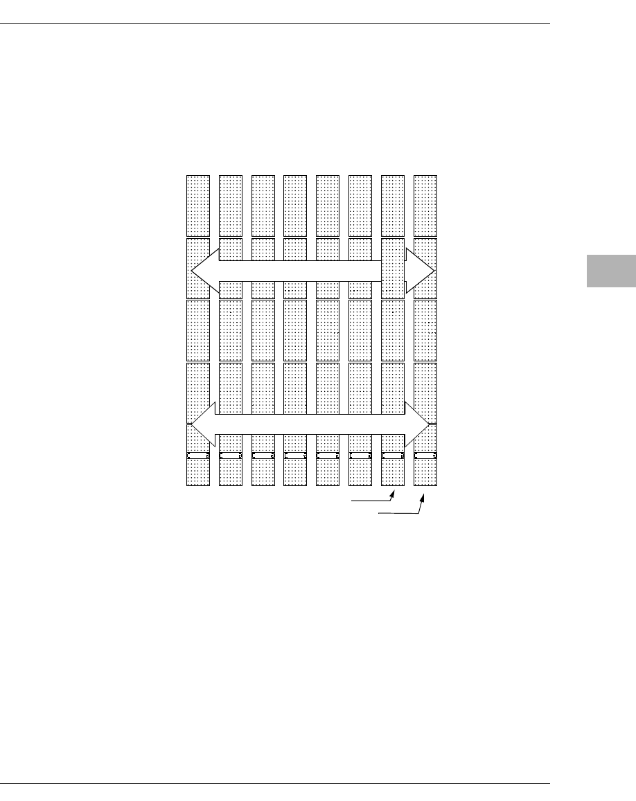
H.110 Bus Connectors—CPX8216T System Only
http://www.motorola.com/computer/literature 6-37
6
H.110 Bus Connectors—CPX8216T System
Only
On each domain, the H.110 bus passes through connector P4 across the I/O
and HSC slots. It does not connect to the CPU slot (see Figure 6-6).
Figure 6-6. The CPX8216T H.110 Bus 2557 9906
P5
P4
P3
P2
P1
H. 110 Bus
CompactPCI Bus
System Slot
HSC Slot
6-38 Computer Group Literature Center Web Site
Subassembly Reference
6
Primary (Front) Side I/O Connectors
The tables in the next few sections provide pin assignments for all I/O,
HSC and CPU slots. For further connector pinouts, refer to the table below.
Primary (Front) Side (Slots 1-6 and 11-16)
The I/O connectors for slots 1-6 and 11-16, except for the P4 connector,
which carries the H.110 bus, use the same pinouts as the standard
CPX8216 backplane.
Pinout Information for
Connector: See:
P5 Table 6-10 on page 6-12
P4 Table 6-32 on page 6-38
P3 Table 6-12 on page 6-12
P2 Table 6-13 on page 6-13
P1 Table 6-14 on page 6-14
Table 6-32. P4 Connector, I/O Slots 1-6, 11-16
POS Row
Z Row A Row B Row C Row D Row E Row
F
25 NP SGA4 SGA3 SGA2 SGA1 SGA0 FG
24 NP GA4 GA3 GA2 GA1 GA0 FG
23 NP +12V CT_RST[n]# CT_EN[n]# -12V CT_MC FG
22 NP PSF0# RSVD RSVD RSVD RSVD FG
NP=Not Populated. P4 implements the full H.110 Bus connections, which requires P4 to use
depopulated connectors.
CT_RST1# through CT_RST6# are routed radially to the bridge slots.
CT_EN1# is connected to BD_SEL1# on the backplane, and so forth.
[n]=n is the slot number.
Refer to the H.110 specifications for line terminations.
Primary (Front) Side (Slots 1-6 and 11-16)
http://www.motorola.com/computer/literature 6-39
6
21 NP -SELVbat PSF1# RSVD RSVD SELVbat RTN FG
20 NP NP NP NP NP NP NP
19 NP NP NP NP NP NP NP
18 NP VRG NP NP NP VRG RTN NP
17 NP NP NP NP NP NP NP
16 NP NP NP NP NP NP NP
15 NP -Vbat NP NP NP Vbat RTN NP
14-12 KEY AREA
11 NP CT_D29 CT_D30 CT_D31 V(I/O) CT_FRAME_A# GND
10 NP CT_D27 +3.3V CT_D28 +5V CT_FRAME_B# GND
9 NP CT_D24 CT_D25 CT_D26 GND FR_COMP# GND
8 NP CT_D21 CT_D22 CT_D23 +5V CT_C8_A GND
7 NP CT_D19 +5V CT_D23 GND CT_C8_A GND
6 NP CT_D16 CT_D17 CT_D18 GND CT_NETREF_1 GND
5 NP CT_D13 CT_D14 CT_D15 +3.3V CT_NETREF_2 GND
4 NP CT_D11 +5V CT_D12 +3.3V SCLK GND
3 NP CT_D8 CT_D9 CT_D10 GND SCLK-D GND
2 NP CT_D4 CT_D5 CT_D6 CT_D7 GND GND
1 NP CT_D0 +3.3V CT_D1 CT_D2 CT_D3 GND
Table 6-32. P4 Connector, I/O Slots 1-6, 11-16 (continued)
POS Row
Z Row A Row B Row C Row D Row E Row
F
NP=Not Populated. P4 implements the full H.110 Bus connections, which requires P4 to use
depopulated connectors.
CT_RST1# through CT_RST6# are routed radially to the bridge slots.
CT_EN1# is connected to BD_SEL1# on the backplane, and so forth.
[n]=n is the slot number.
Refer to the H.110 specifications for line terminations.
6-40 Computer Group Literature Center Web Site
Subassembly Reference
6
Primary (Front) Side CPU Connectors
The CPU connectors on the CPX8216T H.110 backplane use the same
pinouts as the CPX8216 standard backplane.
Primary (Front) Side HSC Connectors
The HSC/Bridge slot is unique. All five connectors (P5 through P1) use
standard tails, and none of the connectors pass through to the rear.
For Pinout Information
for Connector: See:
P5 Table 6-15 on page 6-17
P4 Table 6-16 on page 6-18
P3 Table 6-17 on page 6-20
P2-Domain A Table 6-18 on page 6-20
P2-Domain B Table 6-19 on page 6-22
P1 Table 6-20 on page 6-23
Table 6-33. P5 Connector, HSC/Bridge (Slots 8 and 10)
POS Row Z Row A Row B Row C Row D Row E Row F
25 GND _AD36 _AD35 _AD34 _AD33 _AD32 GND
24 GND _AD40 _AD39 _AD38 _GND _AD37 GND
23 GND _AD45 _AD44 _AD43 _AD42 _AD41 GND
22 GND _AD49 _+3.3 _AD48 _AD47 _AD46 GND
The _GND, _+5 and _+3 in the shaded cells are provided by the CPU board; they are not
connected to the system power plane. These signals are prefixed with CPUA if the board resides
in slot 10 or CPUB if the board resides in slot 8 (for example, CPUA_+5).
Unshaded signals beginning with an underscore (_) are prefixed with the local PCI bus name:
*For boards located in slot 10 (Domain A), the signal name is prefixed with L_PCI_A (for
example, L_PCI_A_AD17).
*For boards located in slot 8 (Domain B), the signal name is prefixed with L_PCI_B (for example,
L_PCI_B_AD17).
Primary (Front) Side HSC Connectors
http://www.motorola.com/computer/literature 6-41
6
21 GND _AD53 _AD52 _AD51 _GND _AD50 GND
20 GND _AD57 _+3.3 _AD56 _AD55 _AD54 GND
19 GND _AD61 _AD60 _AD59 _GND _AD58 GND
18 GND _CBE4# _+3.3 _PAR64 _AD63 _AD62 GND
17 GND _REQ64# _CBE7# _CBE6# _GND _CBE5# GND
16 GND _AD2 _+3.3 _AD1 _AD0 _ACK64# GND
15 GND _AD6 _AD5 _AD4 _GND _AD3 GND
14-
12 KEY AREA
11 GND _AD9 _AD8 _CBE0# _GND _AD7 GND
10 GND _AD13 _+5 _AD12 _AD11 _AD10 GND
9 GND _PAR _CBE1# _AD15 _GND _AD14 GND
8 GND _STOP# _+5 _LOCK# _PERR# _SERR# GND
7 GND _FRAME# _IRDY# _TRDY# _GND _DEVSEL
#
GND
6 GND _AD18 _+5 _AD17 _AD16 CBE2# GND
5 GND _AD21 _CLK _AD20 _GND _AD19 GND
4 GND _CBE3# _+5 _IDSEL _AD23 _AD22 GND
3 GND _AD28 _AD27 _AD26 _AD25 _AD24 GND
Table 6-33. P5 Connector, HSC/Bridge (Slots 8 and 10) (continued)
POS Row Z Row A Row B Row C Row D Row E Row F
The _GND, _+5 and _+3 in the shaded cells are provided by the CPU board; they are not
connected to the system power plane. These signals are prefixed with CPUA if the board resides
in slot 10 or CPUB if the board resides in slot 8 (for example, CPUA_+5).
Unshaded signals beginning with an underscore (_) are prefixed with the local PCI bus name:
*For boards located in slot 10 (Domain A), the signal name is prefixed with L_PCI_A (for
example, L_PCI_A_AD17).
*For boards located in slot 8 (Domain B), the signal name is prefixed with L_PCI_B (for example,
L_PCI_B_AD17).
6-42 Computer Group Literature Center Web Site
Subassembly Reference
6
2 GND _GNT# _REQ# _AD31 _AD30 _AD29 GND
1 GND _INTA# _INTB# _INTC# _INTD# _RST# GND
Table 6-34. P4 Connector, HSC Slots 8 and 10
POS Row
Z Row A Row B Row C Row D Row E Row
F
25 NP SGA4 SGA3 SGA2 SGA1 SGA0 FG
24 NP GA4 GA3 GA2 GA1 GA0 FG
23 NP +12V CT_RST[n]# CT_EN[n]# -12V CT_MC FG
22 NP PSF0# RSVD RSVD RSVD RSVD FG
21 NP -SELVbat PSF1# RSVD RSVD SELVbat RTN FG
20 NP NP NP NP NP NP NP
19 NP NP NP NP NP NP NP
18 NP VRG NP NP NP VRG RTN NP
NP=Not Populated. P4 implements the full H.110 Bus connections, which requires P4 to use
depopulated connectors.
CT_RST1# through CT_RST6# are routed radially to the bridge slots.
CT_EN1# is connected to BD_SEL1# on the backplane, and so forth.
[n]=n is the slot number.
Refer to the H.110 specifications for line terminations.
Table 6-33. P5 Connector, HSC/Bridge (Slots 8 and 10) (continued)
POS Row Z Row A Row B Row C Row D Row E Row F
The _GND, _+5 and _+3 in the shaded cells are provided by the CPU board; they are not
connected to the system power plane. These signals are prefixed with CPUA if the board resides
in slot 10 or CPUB if the board resides in slot 8 (for example, CPUA_+5).
Unshaded signals beginning with an underscore (_) are prefixed with the local PCI bus name:
*For boards located in slot 10 (Domain A), the signal name is prefixed with L_PCI_A (for
example, L_PCI_A_AD17).
*For boards located in slot 8 (Domain B), the signal name is prefixed with L_PCI_B (for example,
L_PCI_B_AD17).
Primary (Front) Side HSC Connectors
http://www.motorola.com/computer/literature 6-43
6
17 NP NP NP NP NP NP NP
16 NP NP NP NP NP NP NP
15 NP -Vbat NP NP NP Vbat RTN NP
14-
12 KEY AREA
11 NP CT_D29 CT_D30 CT_D31 V(I/O) CT_FRAME_A# GND
10 NP CT_D27 +3.3V CT_D28 +5V CT_FRAME_B# GND
9 NP CT_D24 CT_D25 CT_D26 GND FR_COMP# GND
8 NP CT_D21 CT_D22 CT_D23 +5V CT_C8_A GND
7 NP CT_D19 +5V CT_D23 GND CT_C8_A GND
6 NP CT_D16 CT_D17 CT_D18 GND CT_NETREF_1 GND
5 NP CT_D13 CT_D14 CT_D15 +3.3V CT_NETREF_2 GND
4 NP CT_D11 +5V CT_D12 +3.3V SCLK GND
3 NP CT_D8 CT_D9 CT_D10 GND SCLK-D GND
2 NP CT_D4 CT_D5 CT_D6 CT_D7 GND GND
1 NP CT_D0 +3.3V CT_D1 CT_D2 CT_D3 GND
Table 6-34. P4 Connector, HSC Slots 8 and 10 (continued)
POS Row
Z Row A Row B Row C Row D Row E Row
F
NP=Not Populated. P4 implements the full H.110 Bus connections, which requires P4 to use
depopulated connectors.
CT_RST1# through CT_RST6# are routed radially to the bridge slots.
CT_EN1# is connected to BD_SEL1# on the backplane, and so forth.
[n]=n is the slot number.
Refer to the H.110 specifications for line terminations.
6-44 Computer Group Literature Center Web Site
Subassembly Reference
6
Table 6-35. P3 Connector, HSC Slots 8 and 10
POS Row
Z Row A Row B Row C Row D Row E Row
F
19 GND A/B# ALM_B_5
V
INT_HSC_
2
Per3_Pwr_
ON#
Per1_Pwr_
ON#
GND
18 GND HS_REQ_B HS_REQ_A INT_HSC_
1
Per3_LED1
#
Per1_LED1
#
GND
17 GND HS_GNT_B HS_GNT_
A
INT_HSC_
4
Per3_LED2
#
Per1_LED2
#
GND
16 GND HS_FLT_B HS_FLT_A INT_HSC_
3
Per3_PSNT
_B#
Per1_PSNT
_B#
GND
15 GND HS_EJ_B HS_EJ_A INT_HSC_
6
Per4_Pwr_
ON#
Per2_Pwr_
ON#
GND
14 GND INT_HSC_
8
INT_HSC_
7
INT_HSC_
5
Per4_LED1
#
Per2_LED1
#
GND
13 GND A_CLK A_DOUT# PS_1_DIN# Per4_LED2
#
Per2_LED2
#
GND
12 GND B_CLK B_DOUT# PS_2_DIN# Per4_PSNT
_B#
Per2_PSNT
_B#
GND
11 GND ALM_A_F
RAME#
PS_1_FRA
ME#
PS_3_DIN# ALM_A_DI
N#
GND
10 GND ALM_B_F
RAME#
PS_2_FRA
ME#
PS_3_FRA
ME#
B_ENUM# GND
9 GND RST3# RST6# HLTY10# RST16# RST13# GND
8 GND RST2# RST5# HLTY9# RST15# RST12# GND
7 GND RST1# RST4# HLTY8# RST14# RST11# GND
6 GND BD_SEL6# HLTY6# HLTY7# HLTY16# BD_SEL16
#
GND
A/B# GND Domain B (slot 8).
ALM_B_5V in Domain B (slot 8); ALM_A_5V in Domain A (slot 10).
B_ENUM# in Domain B (slot 8); A_ENUM in Domain A (slot 10).
BD_SEL7# in Domain B, BD_SEL9# in Domain A.
Primary (Front) Side HSC Connectors
http://www.motorola.com/computer/literature 6-45
6
5 GND BD_SEL5# HLTY5# BD_SEL7# HLTY15# BD_SEL15
#
GND
4 GND BD_SEL4# HLTY4# RST10# HLTY14# BD_SEL14
#
GND
3 GND BD_SEL3# HLTY3# RST9# HLTY13# BD_SEL13
#
GND
2 GND BD_SEL2# HLTY2# RST8# HLTY12# BD_SEL12
#
GND
1 GND BD_SEL1# HLTY1# RST7# HLTY11# BD_SEL11
#
GND
Table 6-36. P2 Connector, HSC Slot 10
POS Row Z Row A Row B Row C Row D Row E Row F
22 GND GA4 GA3 GA2 GA1 GA0 GND
21 GND CLK6 GND RSV RSV RSV GND
20 GND CLK5 GND RSV GND RSV GND
19 GND GND GND RSV RSV RSV GND
18 GND _BRSVP2
A18
_BRSVP2
B18
_BRSVP2
C18
GND _BRSVP2
E18
GND
17 GND _BRSVP2
A17
GND (_PRST#) _REQ6# GNT6# GND
Signals beginning with an underscore (_) are prefixed with the bus name PCI_B (for example,
PCI_B_AD[49]).
Signals in parentheses are not used.
Table 6-35. P3 Connector, HSC Slots 8 and 10 (continued)
POS Row
Z Row A Row B Row C Row D Row E Row
F
A/B# GND Domain B (slot 8).
ALM_B_5V in Domain B (slot 8); ALM_A_5V in Domain A (slot 10).
B_ENUM# in Domain B (slot 8); A_ENUM in Domain A (slot 10).
BD_SEL7# in Domain B, BD_SEL9# in Domain A.
6-46 Computer Group Literature Center Web Site
Subassembly Reference
6
16 GND _BRSVP2
A16
_BRSVP2
B16
(_DEG#) GND _BRSVP2
E16
GND
15 GND _BRSVP2
A15
GND (_FAL#) REQ5# GNT5# GND
14 GND _AD[35] _AD[34] _AD[33] GND _AD[32] GND
13 GND _AD[38] GND VIO _AD[37] _AD[36] GND
12 GND _AD[42] _AD[41] _AD[40] GND _AD[39] GND
11 GND _AD[45] GND VIO _AD[44] _AD[43] GND
10 GND _AD[49] _AD[48] _AD[47] GND _AD[46] GND
9 GND _AD[52] GND VIO _AD[51] _AD[50] GND
8 GND _AD[56] _AD[55] _AD[54] GND _AD[53] GND
7 GND _AD[59] GND VIO _AD[58] _AD[57] GND
6 GND _AD[63] _AD[62] _AD[61] GND _AD[60] GND
5 GND _C/BE[5]# GND VIO C/BE[4]# _PAR64 GND
4 GND VIO _BRSVP2
B4
_C/BE[7]# GND _C/BE[6] GND
3 GND CLK4 GND GNT3# REQ4# GNT4# GND
2 GND CLK2 CLK3 _SYSEN# GNT2# REQ3# GND
1 GND CLK1 GND REQ1# GNT1# REQ2# GND
Table 6-36. P2 Connector, HSC Slot 10 (continued)
POS Row Z Row A Row B Row C Row D Row E Row F
Signals beginning with an underscore (_) are prefixed with the bus name PCI_B (for example,
PCI_B_AD[49]).
Signals in parentheses are not used.
Primary (Front) Side HSC Connectors
http://www.motorola.com/computer/literature 6-47
6
Table 6-37. P2 Connector, HSC Slot 8
POS Row Z Row A Row B Row C Row D Row E Row F
22 GND GA4 GA3 GA2 GA1 GA0 GND
21 GND CLK16 GND RSV RSV RSV GND
20 GND CLK15 GND RSV GND RSV GND
19 GND GND GND RSV RSV RSV GND
18 GND _BRSVP2
A18
_BRSVP2
B18
_BRSVP2
C18
GND _BRSVP2
E18
GND
17 GND _BRSVP2
A17
GND (_PRST#) _REQ16# GNT16# GND
16 GND _BRSVP2
A16
_BRSVP2
B16
(_DEG#) GND _BRSVP2
E16
GND
15 GND _BRSVP2
A15
GND (_FAL#) REQ15# GNT15# GND
14 GND _AD[35] _AD[34] _AD[33] GND _AD[32] GND
13 GND _AD[38] GND VIO _AD[37] _AD[36] GND
12 GND _AD[42] _AD[41] _AD[40] GND _AD[39] GND
11 GND _AD[45] GND VIO _AD[44] _AD[43] GND
10 GND _AD[49] _AD[48] _AD[47] GND _AD[46] GND
9 GND _AD[52] GND VIO _AD[51] _AD[50] GND
8 GND _AD[56] _AD[55] _AD[54] GND _AD[53] GND
7 GND _AD[59] GND VIO _AD[58] _AD[57] GND
6 GND _AD[63] _AD[62] _AD[61] GND _AD[60] GND
5 GND _C/BE[5]# GND VIO C/BE[4]# _PAR64 GND
4 GND VIO _BRSVP2
B4
_C/BE[7]# GND _C/BE[6] GND
3 GND CLK14 GND GNT13# REQ14# GNT14# GND
Signals beginning with an underscore (_) are prefixed with the bus name PCI_A (for example,
PCI_A_AD[49]).
Signals in parentheses are not used.
6-48 Computer Group Literature Center Web Site
Subassembly Reference
6
2 GND CLK12 CLK13 _SYSEN# GNT12# REQ13# GND
1 GND CLK11 GND REQ11# GNT11# REQ12# GND
Table 6-38. P1 Connector, HSC Slots 8 and 10
POS Row
Z Row A Row B Row C Row D Row E Row
F
25 GND 5V _REQ64# A_ENUM
#
3.3V 5V GND
24 GND _AD[1] 5V VIO _AD[0] _ACK64# GND
23 GND 3.3V _AD[4] _AD[3] 5V _AD[2] GND
22 GND _AD[7] GND 3.3V _AD[6] _AD[5] GND
21 GND 3.3V _AD[9] _AD[8] _M66EN _C/BE[0]
#
GND
20 GND _AD[12] GND VIO _AD[11] _AD[10] GND
19 GND 3.3V _AD[15] _AD[14] GND _AD[13] GND
18 GND _SERR# GND 3.3V _PAR _C/BE[1] GND
17 GND 3.3V _SDONE _SBO# GND _PERR# GND
16 GND _DEVSEL# GND VIO _STOP# _LOCK# GND
15 GND 3.3V _FRAME# _IRDY# BD_SEL[n]# _TRDY# GND
14-
12 KEY AREA
11 GND _AD[18} _AD[17] _AD[16] GND _C/BE[2]
#
GND
A_ENUM# in Domain A (slot 10); B_ENUM# in Domain B (slot 8).
Table 6-37. P2 Connector, HSC Slot 8 (continued)
POS Row Z Row A Row B Row C Row D Row E Row F
Signals beginning with an underscore (_) are prefixed with the bus name PCI_A (for example,
PCI_A_AD[49]).
Signals in parentheses are not used.
Primary (Front) Side HSC Connectors
http://www.motorola.com/computer/literature 6-49
6
10 GND _AD[21] GND 3.3V _AD[20] _AD[19] GND
9 GND _C/BE[3] _IDSEL _AD[23] GND _AD[22] GND
8 GND _AD[26] GND VIO _AD[25] _AD[24] GND
7 GND _AD[30] _AD[29] _AD[28] GND _AD[27] GND
6 GND REQ[N]# GND 3.3V CLK[N] _AD[31] GND
5 GND _BRSVP1A5 _BRSVP1B5 RST[N]# GND GNT[N]# GND
4 GND _BRSVP1A4 HLTY[N]# VIO _INTP _INTS GND
3 GND _INTA# _INTB# _INTC# 5V _INTD# GND
2 GND TCK 5V TMS TDO TDI GND
1 GND 5V -12V TRST# +12V 5V GND
Table 6-38. P1 Connector, HSC Slots 8 and 10 (continued)
POS Row
Z Row A Row B Row C Row D Row E Row
F
A_ENUM# in Domain A (slot 10); B_ENUM# in Domain B (slot 8).
6-50 Computer Group Literature Center Web Site
Subassembly Reference
6
Secondary (Rear) Side I/O Connectors
Note I/O slot connectors P4, P2, and P1 do not connect through to the
transition module.
Secondary (Rear) Side CPU Transition Module
Connectors
The CPU transition module connectors use the same pinouts as the
connectors in the CPX8216 standard backplane.
Note CPU connectors P4, P2, and P1 do not pass through the
backplane.
Table 6-39. P5 Connector, I/O Slots 1-6 and 11-16 (User
I/O)
POS Row Z Row A Row B Row C Row D Row E Row F
22-1 GND I/O I/O I/O I/O I/O GND
All I/O pins pass through the backplane to the transition module, they do not
make any connection to the backplane.
Table 6-40. P3 Connector, I/O Slots 1-6 and 11-16 (User
I/O)
POS Row Z Row A Row B Row C Row D Row E Row F
19-1 GND I/O I/O I/O I/O I/O GND
All I/O pins pass through the backplane to the transition module, they do not
make any connection to the backplane.
For Pinout Information
for Connector: See:
P5 Table 6-24 on page 6-27
P3 Table 6-25 on page 6-28
Alarm Display Panel
http://www.motorola.com/computer/literature 6-51
6
Alarm Display Panel
The alarm display panel provides the system LEDs and remote alarm
functions for the CPX8216 and the CPX8216T. It is powered and
controlled from each of the two Hot Swap Controllers within the system
(see Figure 6-7).
Figure 6-7. Alarm Display Panel Block Diagram
The alarm display panel features three system status LEDs, three Telco
alarm status LEDs, three slot status LEDs for each slot, and an RJ-45
connector for Telco alarm status output to an external interface (see Figure
6-8). Normally, only two of the three slot status LEDs are visible—the
third is covered by the panel’s overlay.
o
oo
o o o
oo
Alarm PLD
Domain A
Logic
Uncommitted
HSC IFC Conn
Domain B
Logic
Digital Inputs
Slot 15 LEDs
REG
GND
POR
PWR A
PWR B
Slot 11 LEDs
Slot 6 LEDs
Slot 2 LEDs
Slot 1 LEDs
Telco
Data B
Frame B
Clock B
System LEDs
Clock A
POWER
Frame A
DIN A
DOUT A
Relay
LEDs
System Alarm Conn
o
o
o
o
o
o
6-52 Computer Group Literature Center Web Site
Subassembly Reference
6
Figure 6-8. Alarm Display Panel—Front View
The alarm display panel LEDs are controlled by bits in the Hot Swap
Controller’s register, which are set by the system software. This allows full
user customization of alarm event reporting. The next table provides the
color and standard nomenclature for the LEDs on the alarm panel.
123456789101112 13 14 15 16
MINOR MAJOR CRI TICAL
TELCO
SYSTEM COMPONENT
SYSTEM
IN SERVICE OUT OF SERVICE
ALARM
CONNECTI ONSTATUS
STATUS
COMPONENT
Table 6-41. Alarm LED Color and Description
Alarm LED Color Description
Controller Board Slot
Status
Green In Service
Yellow N/A (or Out of Service)
Red Out of Service
System Status
Green System In Service
Yellow Component Out of Service
Red System Out of Service
Telco Status
Yellow Minor
Red Major
Red Critical
Alarm Display Panel Interface Connector (J4)
http://www.motorola.com/computer/literature 6-53
6
Alarm Display Panel Interface Connector (J4)
Connector J4 receives system alarm signals from the backplane connector
ALARM.
Remote Alarm Connector (J1)
The RJ-45 remote alarm connector (J1) provides standard telco alarm
signals to remote alarm equipment. The connector also has a jacket shield
to protective earth ground through two separate pins (E1 and E2).
Table 6-42. Alarm Display Panel Interface Connector (J4)
Pin Signal Pin Signal
1 ALM_A_CLK 2 GND
3 ALM_B_CLK 4 GND
5 ALM_A_DOUT# 6 ALM_A_5V
7 ALM_B_DOUT# 8 ALM_B_5V
9 ALM_A_FRAME# 10 ALM_B_FRAME#
11 ALM_A_DIN# 12
13 14
Table 6-43. Remote Alarm Connector (J1)
PinSignalSignalPin
1 Critical Alarm Minor Alarm 5
2 Critical Alarm Return Minor Alarm Return 6
3 Major Alarm Rack Alarm 7
4 Major Alarm Return Rack Alarm Return 8
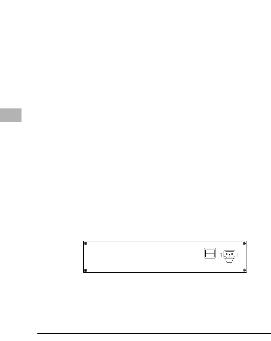
6-54 Computer Group Literature Center Web Site
Subassembly Reference
6
Power Distribution Panel
The power distribution panel, located in the rear of the chassis below the
transition module cardcage, distributes the AC or DC input power to the
system’s power supplies.
There are three versions of the power distribution panel:
❏AC (CPX8216)
❏Dual Input DC (CPX8216)
❏Dual Breaker DC (CPX8216)
❏H.110 DC (CPX8216T)
The CPX8216T can be configured with AC or DC power, however only
the DC version has the dual input option and the H.110 bus analog voltage
inputs.The H.110 bus on P4/J4 operates without the analog voltages
present, but if analog cards are being used (for example, line or trunk
cards) the analog voltages are required.
If the system requires the analog H.110 bus, voltages need to use the dual
DC power distribution panel. If the system requires an AC configuration,
a special AC power distribution panel must be used. Contact your
Motorola sales representative for information.
AC Power Distribution Panel (CPX8216)
The AC version of the panel is shown in the figure below.
Figure 6-9. AC Power Distribution Panel—Front View
l
0
90-260 VAC

Dual Input DC Power Distribution Panel (CPX8216)
http://www.motorola.com/computer/literature 6-55
6
Dual Input DC Power Distribution Panel (CPX8216)
The dual input DC version allows redundant input power supplies for full
high-availability applications. It is recommended that each input source be
independent of the other.
Figure 6-10. Dual Input DC Power Distribution Panel—Front View
Use 12 AWG or larger wire with a #10 ring terminal to connect the DC
power source to the system.
Dual Breaker DC Power Distribution Panel (CPX8216)
The dual breaker 48VDC version also allows redundant input power
supplies for full high-availability applications. It is recommended that each
input source be independent of the other. This power distribution panel has
two 30A push/pull circuit breakers and is designed for use with a Smart
cable that includes breakers and additional circuitry that detect the failure
of a single input DC power supply.
2572 9907
-48 VDC
-48 VDC RTN
-48 VDC
-48 VDC RTN
ON ON
Ring Terminal
WIDTH
STUD SIZE: #10
WIDTH: .490 inch (12.446 mm) or smaller
WIRE GAGE: 12AWG or bigger
6-56 Computer Group Literature Center Web Site
Subassembly Reference
6
Figure 6-11. Dual Breaker DC Power Distribution Panel—Front View
The dual breaker DC power distribution panel is available without the two
30A circuit breakers, provided that circuit breaker protection is provided
elsewhere and there is allowance for a rating of 30A for each feed.
Use either a standard Smart cable or the optional right-angle Smart cable
(for limited space requirements) to connect the DC power source to the
system. Cable length is 10 feet.
H.110 DC Power Distribution Panel (CPX8216T)
The H.110 DC power distribution panel provides dual DC input for system
power as well six additional power input connectors for the H.110 BAT
and Ring Voltages. The H.110 DC power distribution panel is only
compatible with the CPX8216T system.
!
Caution
Ca ution The six H.110 power inputs must only be attached to approved Telephone
Network Voltage (TNV) branch circuits. TNV branch circuits must
comply with all requirements called for in these safety standards: IEC
950/EN60 950, UL #1950, and CSA #950. Attaching those inputs to non-
TNV-approved power sources will cause the system to fail compliance
with safety regulations and may cause damage to the system backplane and
system components.
Part Number Cable Description
30-W2750E01A Standard Smart cable
30-W2750E03A Right-angle Smart cable
H.110 DC Power Distribution Panel (CPX8216T)
http://www.motorola.com/computer/literature 6-57
6
Figure 6-12. H.110 DC Power Distribution Panel
The analog voltages on the H.110 bus are:
Use 12 AWG or larger wire with a #10 ring terminal to connect the DC
system power source to the system. Use 12 AWG or larger wire with a #6
ring terminal to connect the DC TNV voltages to the H.110 power
connectors.
2573 9907
-48 VDC
-48 VDC
-48 VDC
-48 VDC
ON ON
RTN
-VBAT
VBAT RTN
VRG
VRG RTN
-SEL VBAT
SEL VBAT RTN
RTN
System Power
Terminal Blocks
H.110 BAT and
Ring Voltage
Terminal Block
Table 6-44. DC Analog Voltages for H.110 Bus
Description Voltage Inputs
Battery -48V DC
Return Nominal 48V, range of 40V to 72V
Ringing 90 VAC nominal
SELV 24V DC nominal, range of <60V
Ring Terminal - System Power
WIDTH
STUD SIZE: #10
WIDTH: .490 inch (12.446 mm) or smaller
WIRE GAGE: 12AWG or bigger
Ring Terminal - H.110 Power
STUD SIZE: #6
WIRE GAGE: 12AWG or bigger

Power Supplies
http://www.motorola.com/computer/literature 6-58
6
Power Supplies
The AC and DC power supplies are mounted on a sled along with the
replaceable cooling fans and are discussed in the CPX8000 Series
CPX8216 and CPX8216T System Installation and Use manual.
For the power coupling to the backplane, refer to the information in Power
Supply Connectors (PS1, PS2, PS3) on page 6-6. For the electrical
specification for the power supply, refer to Power Supply Electrical
Specifications on page A-2.

A
A-1
ASpecifications
Environmental Characteristics
ENVIRONMENTAL CHARACTERISTICS
Temperature
Operating: 0º to 50º C (32º to 122º F) continuous duty with linear current derating
between +50º C to +60º C (122º to 140º F) to 50% maximum rated power
Storage and Transit: -25º TO +85º C (-13º to 185º F)
Maximum Altitude
Operating: Linear current derating to 85% between 8,000 feet and 12,000 feet
Storage and Transit: 30,000 feet
Shock No degradation at 25g shock of 11ms duration at 1/2 sine wave in three
planes.
Vibration No degradation at sine 10 to 100 to 10Hz to 2g 10min/decade three planes.
Meets NEBS Bellcore TR-NWT-000063, Zone 4 Earthquake Vibration
Acoustic Noise Maximum sound level 70dbA (measured at 1 meter from the power supply
at all points around it using a sound-level meter meeting ANSI Standard
S1.4-1983, General Purpose Sound-Level Meter)
Cooling The power supply meets all specifications when cooled by the fan in its
subenclosure within the restriction of the system enclosure.

A-2 Computer Group Literature Center Web Site
Specifications
A
Power Supply Electrical Specifications
AC Input AC Voltage: 90 Vac to 132 Vac or 190 Vac to 260 Vac (autoranging)
AC Frequency: 47 Hz to 63 Hz
Power Factor: Minimum 0.98 at full load and nominal line
Turn-on Surge Current: 20 Amps at +/- 2A for one line cycle
Efficiency: -72% typical at full load and nominal line, including output Oring diodes
Input Current: Measured 6.0A maximum at 115 Vac, 3A maximum at 230 Vac at
475 watts
DC Input DC Voltage: -36 Vdc to -72 Vdc (autoranging)
Turn-on Threshold: -38.5 Vdc to -41Vdc
Turn-on Surge Current: 20 Amps at -36 Vdc maximum in less than 4 msec.
Efficiency: 70% minimum at full load and nominal line, including output Oring
diodes
Input Current: Measured 13A @ -48 Vdc at 475W
Output All measurements are made at the output connector of the power supply. The power
supply is used in an N+1 power system. Each voltage output supports power sharing.
Minimum Load Operation: None
Total Regulation: Total regulation is any combination of line, load and cross
regulation, actual set point (as a deviation from the nominal set point), warm up, and
temperature that results in an output voltage that deviates from the nominal set point.
Table A-1 provides the total regulation for each output:
Power Supply Electrical Specifications
http://www.motorola.com/computer/literature A-3
A
Table A-1. Total Regulation (per Output)
Output
Number Voltage Set Point at Load Maximum
Current Loads Total
Regulation
V1 +5.0V +5.06Vdc@20A
+/- 5 mV
40A 0 to 40A ±3%
V2 +3.3V +3.36Vdc@20A
+/- 5 mV
40A 0 to 40A ±3%
V3 +12.0V +12.1Vdc@4A
+/- 24 mV
10.4A cont.
(11.5A peak
for max. 5
sec.)
0 to 10.4A ±5%
V4 -12.0V -12.1Vdc@2A
+/- 12 mV
4A 0 to 4A ±5%
Output Power 400 Watts total continuous maximum from all outputs. Any mix of
outputs totaling 400W is acceptable.
DC Output Voltage
Adjustment No output adjustments.
Output Noise Total periodic and random deviation (PARD) noise found on outputs of
the power module shall be, as measured at the backplane:
-From 0 to 30 MHz bandwidth for ripple <50 mV
-From 0 to 100 MHz bandwidth for spikes <75 mV
Overload Protection All DC outputs have a method to protect the power supply from overloads
and shorts. When one output is overloaded, then all outputs are turned off.
Cycling the AC or DC input off then on will cause the power supply to
attempt recovery.
Output to Output Short
Protection The power supply provides protection when any output is shorted to any
other output. A short is considered to be any interconnection that results
in any output deviating from its regulation range by more than 0.7 Volts.
Cycling the AC or DC input off then on will cause the power supply to
attempt recovery.

A-4 Computer Group Literature Center Web Site
Specifications
A
Overshoot Overshoot does not exceed 2.0% of any output voltage under the
following conditions: power failure, enabled, disabled, and AC input
cycled on/off. Overshoot is the phenomena where the magnitude of
voltage of an output temporarily exceeds its final or stabilized value.
Load Change Transient
Response Any DC voltage returns to 1% within 2mS in response to a 25% change
in the load. The +5V output does not vary more than 3% in response to a
25% change in load. The 12V output does not go out of regulation during
a 0.5A change in the +12V load.
Proper Operation
During Dynamic Loads The power supply operates properly when subjected to a 10% delta
dynamic load with a 50% duty cycle at all frequencies from zero to 2
MHz, or 2 times the switching frequency of the power supply, whichever
is greater.
Undershoot and Reverse
Voltage With respect to its normal zero reference voltage, no output voltage,
under any normal condition, become of a polarity opposite to its normal
operation polarity (excluding applying an external reverse voltage).
Output Risetime The +5V output will have a monotonic rise from 2V to 4.75V. The +5V
output will transition from +2V to +4.75V in less than 50mS when loaded
to 37.5A or less.
The +5V output will always be above +3.3V output.
The +3.3V output will transition from +2V to 13.3V in less than 50mS.
The skew in risetime between +5V and +3.3V outputs will be less than 50
mS.
The +12V output will transition from +2V to +10.8V in less than 50 mS.
The above conditions will be over the complete input range and load
range, from minimum to maximum load with a capacitive load.
Holdover Storage Output voltage stays within regulation limits for at least 20 msec. from
the last peak of the line voltage cycle after input power is removed. The
power supply does not latch off during an AC line loss condition that is
less than the hold up time.

Power Supply Electrical Specifications
http://www.motorola.com/computer/literature A-5
A
Over Voltage Protection A Single Fault condition is the failure of any one device within the power
supply. The condition includes both the shorting of any output and the
failure of any one device within the power supply.
Under any single fault condition:
The +5V outputs limit voltage at 6.4Vdc maximum.
The +3.3V output limits voltage at 4.2Vdc maximum
The ±12V outputs do not exceed ±15.0Vdc, respectively.
Control Signals ENABLE POWER# (Input to Power Supply):
Turns on and off the power supply outputs. When the Enable Power#
signal is low, the power supply will be ON. When the Enable Power#
signal is high or open, the power supply will be OFF.
POWER GOOD# (Output from Power Supply):
This signal is low when the power supply output voltages are good. The
signal is high when the power supply voltages are bad. The voltage is
good when it is within ±5% of the set voltage.
B-1
B
BRelated Documentation
Motorola Computer Group Documents
The Motorola publications listed below are referenced in this manual. You
can obtain paper or electronic copies of Motorola Computer Group
publications by:
❏Contacting your local Motorola sales office
❏Visiting MCG’s World Wide Web literature site,
http://www.motorola.com/computer/literature
❏To locate and view the most up-to-date product information in
PDF or HTML format, visit
http://www.motorola.com/computer/literature.
Document Title Motorola
Publication Number
Compact PCI CPX8216 and CPX8216T System Installation and
Use
CPX8216A/IH
MCP750HA Hot Swap CompactPCI Single Board Computer
Installation and Use
MCP750HA/IH
MCP750 CompactPCI Single Board Computer Installation and
Use
MCP750A/IH
MCP750 Single Board Computer Programmer’s Reference Guide MCP750A/PG
PPCBug Firmware Package User’s Guide PPCBUGA1/UM, and
PPCBUGA2/UM
B-2 Computer Group Literature Center Web Site
Related Documentation
B
Related Specifications
For additional information, refer to the following table for related
specifications. For your convenience, a source for the listed document is
also provided. It is important to note that in many cases, the information is
preliminary and the revision levels of the documents are subject to change
without notice.
TMCP700 Transition Module Installation and Use TMCP700A/IH
CPV5350 CompactPCI Single Board Computer and Transition
Module installation and Reference
CPV5350A/IH
CPV8540 CompactPCI Hot Swap Carrier Card User Manual
(Single PMC)
CPV8540A/UM
CPV8540 CompactPCI Hot Swap Carrier Card User Manual (Dual
PMC)
CPV8540B/UM
Document Title Motorola
Publication Number
Table B-1. Related Specifications
Document Title and Source Publication
Number
Electronic Industries Alliance http://www.eia.org/
Interface Between Data Terminal Equipment and Data Circuit-
Terminating Equipment Employing Serial Binary Data Interchange;
Electronic Industries Alliance;
http://global.ihs.com/index.cfm (for publications)
TIA/EIA-232
Standard
IEEE http://standards.ieee.org/catalog/
Related Specifications
http://www.motorola.com/computer/literature B-3
B
Versatile Backplane Bus: VMEbus
Institute of Electrical and Electronics Engineers, Inc.
OR
Microprocessor system bus for 1 to 4 byte data
Bureau Central de la Commission Electrotechnique Internationale
3, rue de Varembé
Geneva, Switzerland
ANSI/IEEE
Standard 1014-1987
IEEE Standard for Compact Embedded PC Modules IEEE P996.1
IEEE - Common Mezzanine Card Specification (CMC)
Institute of Electrical and Electronics Engineers, Inc.
P1386 Draft 2.0
IEEE - PCI Mezzanine Card Specification (PMC)
Institute of Electrical and Electronics Engineers, Inc.
P1386.1 Draft 2.0
Bidirectional Parallel Port Interface Specification
Institute of Electrical and Electronics Engineers, Inc.
IEEE Standard 1284
PCI Industrial Manufacturers Group (PICMG) http://www.picmg.com/
Compact PCI Specification CPCI Rev. 2.1
Dated 9/2/97
PCI-to-PCI Bridge Specification
PCI-ISA Specification
Rev. 1.02
Rev. 2.0
CompactPCI Hot Swap Specification
PCI Industrial Computers Manufacturers Group (PICMG)
PIMCG 2.1 R1.0
PCI Special Interest Group (PCI SIG) http://www.pcisig.com/
Peripheral Component Interconnect (PCI) Local Bus Specification,
Revision 2.0, 2.1, 2.2
PCI Special Interest Group;
PCI Local Bus
Specification
Table B-1. Related Specifications (continued)
Document Title and Source Publication
Number

B-4 Computer Group Literature Center Web Site
Related Documentation
BURLs
The following URLs (uniform resource locators) may provide helpful
sources of additional information about this product, related services, and
development tools. Please note that, while these URLs have been verified,
they are subject to change without notice.
❏Motorola Computer Group, http://www.motorola.com/computer
❏Motorola Computer Group OEM Services,
http://www.motorola.com/computer/support
❏Technobox Inc.,
http://www.technobox.com

IN-1
A
AC power input A-2
acoustic noise A-1
adapters, PMC 4-1
alarm board. See alarm display panel
alarm display panel 1-13, 6-51 to 6-53
alarm interface connector 6-8
altitude, operating A-1
B
backplane
connectors 6-6
reference 6-5
board insertion, features 1-14
branch circuits, TNV 6-56
bridge connector slots 6-29
bus access in CPX8216T 1-4
bus connectors, H.110 6-37
bus segments 1-1
bus, PCI 2-2
C
cables
DC power cable 6-55
card cage reference 6-4
carrier card
diagram 3-2
features 3-1
chassis ID 1-13
circuit breakers 6-56
COM connectors (CPV5350) 2-22
COM connectors (CPV5350TM80) 5-33
COM connectors (CPX750A) 2-5
COM connectors (CPX750HATM) 5-6
Compact Flash connector 2-14
CompactPCI board standards 6-5
CompactPCI connectors 6-11 to 6-35
CompactPCI Hot Swap specification 1-1
conditions for HSC control 1-6
configurations
active/active 1-9
I/O 1-10
processor 1-7
simplex 1-7
configuring ports 5-18, 5-28
connectors (CPV5350)
COM 2-22
Ethernet 2-21
keyboard/mouse 2-20
USB 2-21
video 2-22
connectors (CPV5350TM80)
COM1/COM2 5-33
Ethernet 5-33
parallel port 5-35
serial port 5-33
video 5-34
connectors (CPX750HA)
COM 2-5
debug 2-6
DRAM mezzanine 2-10
EIDE compact flash 2-14
Ethernet 2-4
USB 2-4
connectors (CPX750HATM)
backplane 5-4
COM 5-6
floppy port 5-12
I/O 5-5, 5-6
keyboard/mouse 5-10
parallel port 5-9
serial port 5-6, 5-7
transition module 5-4
Index

IN-2 Computer Group Literature Center Web Site
I
N
D
E
X
USB 5-10
connectors (CPX8216)
alarm 6-8
alarm display panel 6-53
CPU slot 6-17
fan module 6-7
floppy drive 6-8
HSC/bridge 6-29
I/O 6-11
I/O slot 6-26
IDE drive 6-9
power 6-10
power supply 6-6
signal 6-11
transition module 6-27
connectors (CPX8216T)
bus, H.110 6-37
CPU 6-40
fan module 6-7
HSC 6-40, 6-48
I/O 6-38, 6-50
power 6-7
transition module 6-50
connectors (CPX8540)
32-bit PCI 3-5, 3-7
64-bit (PMC) 3-8
I/O 3-4
controller, SCSI-2 4-1
conventions used in the manual xxiii
cooling A-1
CPU connectors, H.110 6-40
CPU module, features 1-12
CPU service switchover 1-13
CPU slot connectors 6-17
CPV5350
board connectors 2-18
component layout 2-19
Ethernet connector 2-21
features 2-16
indicator lights 2-16
keyboard/mouse connector 2-20
memory DIMM 2-20
memory expansion 2-20
CPV5350TM80
board headers 5-31
connectors 5-31
EIDE headers 5-36
Ethernet connector 5-33
fan tach header 5-43
features 5-29
floppy header 5-38
indicator LED header 5-43
keyboard/mouse/power LED
header 5-40
parallel port connectors 5-35
serial port connectors 5-33
SM Bus/LM78header 5-42
USB header 5-41
video connectors 5-34
CPX750HA
bus capacity 2-2
COM connector 2-5
debug connector 2-6
DRAM mezzanine connector 2-10
EIDE compact flash connector 2-14
Ethernet connectors 2-4
features 2-1
I/O peripherals 2-2
PCI bus 2-2
USB connectors 2-4
CPX750HATM
backplane connectors 5-4
configuring ports 5-18 to 5-28
connectors 5-4
EIDE connector 5-11
features 5-1
I/O connectors 5-4, 5-5
jumper settings 5-4
keyboard/mouse connector 5-10
parallel port connector 5-9
PMC I/O connector 5-14
power connector 5-12
serial port configuration 5-2
serial port connectors 5-7

http://www.motorola.com/computer/literature IN-3
I
N
D
E
X
SIMs 5-16
speaker connector 5-13
USB connectors 5-10
CPX8216
bus access 1-4
CPU modules 1-12
hot swap controller 1-12
standard system 1-2
subsystems 1-2
system description 1-1
CPX8216T
bus connectors, H.110 6-37 to 6-50
chassis ID 1-13
H.110 system 1-2
power connector
ring voltage 6-7
power distribution panel, DC 6-56
telephony bus 1-14
CPX8540
carrier card 3-1
features 3-1
installing PMC modules 3-2
D
DC power input A-2
debugging 2-6
default conditions 1-6
device drivers 1-19
domain control 1-1, 1-4, 1-6
domains, HSC 6-29
domains, IDE drive 6-9
DRAM memory 2-20
DRAM mezzanine connector 2-10
dual HSC 1-6
dual system 1-9
E
EIDE connector 5-11
electrical specifications, power supply A-2
environmental specifications A-1
ESD clips 6-4
Ethernet connectors 2-4
Ethernet connectors (CPV5350) 2-21
F
fan module 6-7
flash memory 2-15
floppy drive connectors 6-8
floppy port connector 5-12
front panel, CPV5350 2-16
front panel, CPX750HATM 5-6
G
grounding 5-9, 6-6
H
H.110
BAT and Ring Voltages 6-56
I/O connectors, secondary 6-50
power connector 6-7
power distribution panel 6-56
transition module connectors 6-50
H.110 bus analog voltage 6-54, 6-57
headers
EIDE 5-36
fan tach 5-43
floppy 5-38
indicator LED 5-43
keyboard/mouse/power LED 5-40
SM Bus/LM78 5-42
USB 5-41
hot swap controller 1-6
connector 6-29
connector, H.110 6-40, 6-48
functions 1-5
system software 1-7
hot swap features
control status register 1-14
signals 1-14
staged pins 1-14
hot swap process 1-16 to 1-19
HSC. See hot swap controller

IN-4 Computer Group Literature Center Web Site
I
N
D
E
X
I
I/O connectors, H.110 6-38
I/O connectors, primary 6-11
I/O connectors, secondary 6-26
I/O devices 1-10
I/O interfaces, PCI bus 2-2
I/O slots 6-4
IDE drive connectors 6-9
initialization state 1-6
installing
fan module 6-7
PMC modules 3-2
SIMs 5-16
ISA bus functions 2-2
J
J10 connector 2-10
J11 connector 2-5
J15 connector 2-5
J17 connector 2-4
J18 connector 2-4
J19 connector 2-6
J8 connector 2-4
J9 connector 2-14
jumper settings
Flash selection 2-15
SCSI-2 4-3
serial port 5-4
SIMs 5-16
L
LED indicator lights 2-16
LEDs, description 6-52
load sharing restrictions 1-7, 1-9
load-sharing configuration 1-9
logical system domains 1-1
M
manual conventions xxiii
memory banks 2-15
memory expansion 2-20
modules
HSC 1-5
PMC 3-1
MPMC150
features 4-1
pin assignments 4-4
switch settings 4-3
MPU processor bus 2-6
O
output power A-3
P
parallel port signals 5-9
PCI bus 2-2
I/O interfaces 2-2
peripherals, using in system 1-11
pin assignments
alarm connector 6-8
CPX750HA
EIDE compact flash 2-14
I/O slots H.110 6-38
pin assignments (CPV5350)
Ethernet 2-21
keyboard/mouse 2-20
serial port 2-22
USB 2-21
video 2-22
pin assignments (CPV5350TM80)
EIDE 5-36
Ethernet 5-33
fan tach 5-43
floppy header 5-38
indicator LED 5-43
keyboard/mouse/power LED 5-40
parallel port 5-35
serial port 5-33
SM BUS/LM78 5-42
USB 5-41
video 5-34
pin assignments (CPX750HA)
COM1 2-5
debug 2-6

http://www.motorola.com/computer/literature IN-5
I
N
D
E
X
DRAM mezzanine 2-10
Ethernet 2-5
USB 2-4
pin assignments (CPX750HATM)
COM1/COM2 5-6
EIDE connector 5-11
floppy port 5-12
I/O connector 5-5, 5-6
keyboard/mouse 5-10
parallel port 5-9
PMC I/O connector 5-14
power connector 5-12
serial port 5-7
speaker connector 5-13
pin assignments (CPX8216)
alarm display panel connector 6-53
CPU slots 6-17
fan module 6-7
floppy connector 6-8
HSC/bridge 6-29
I/O 6-11
I/O slots 6-26
IDE drive 6-9
power connector 6-10
signal connectors 6-11
transition module slots 6-27
pin assignments (CPX8216T)
fan module 6-7
H.110 power connector 6-7
HSC 6-40 to 6-48
I/O connectors 6-50
pin assignments (CPX8540) 3-4 to 3-9
I/O 3-4
PCI 32-bit 3-5, 3-7
PCI 64-bit 3-8
pin assignments (MPMC150) 4-4
PMC adapter pin assignments 4-4
PMC carrier card
expansion 2-2
features 3-1
I/O connector 5-14
PMC module
adding 3-2
features 4-1
port configurations 5-18, 5-28
port signals 5-9
power
approved sources 6-56
distribution 6-54
dual breaker distribution panel 6-55
dual input distribution panel 6-55
output A-3
power connectors 5-12, 6-10
power distribution panel, 48 VDC 6-55
power distribution panel, AC 6-54
power distribution panel, DC dual 6-55
power distribution panel, DC, H.110 6-56
power supplies, electrical specifications A-2
power supplies, in simplex configuration 1-7
power supply connectors 6-6
R
rear panel, CPV5350TM80 5-29
remote I/O bus 1-5
replaceable fan module 6-7
restrictions, load sharing 1-7, 1-9
S
safety standards 6-56
SCSI-2 controller 4-1
SCSI-2 jumpering 4-3
selecting flash banks 2-15
serial interface modules (SIMs) 5-16
serial port
(CPV5350) 2-22
(CPX750HATM) 5-2
CPV5350TM80 5-33
signals 5-7
service switchover 1-13
setting the chassis ID 1-13
shock A-1
signal connectors 6-11
simplex configuration, power supplies 1-7
smart cable 6-55, 6-56

IN-6 Computer Group Literature Center Web Site
I
N
D
E
X
software and the HSC 1-7
speaker connector 5-13
specifications
electrical A-2
environmental A-1
status indicators 2-16
status LEDs 1-13, 6-51
switch settings
MPMC150 4-3
PMC Adapter 4-3
system
active/active configuration 1-9
architecture 1-4
configurations 1-4
device drivers 1-19
EIDE devices 1-11
peripherals 1-10
SCSI devices 1-11
simplex configuration 1-7
slots 6-4
status LEDs 1-13, 6-51
system domains, description 1-1
T
Telephone Network Voltage (TNV) 6-56
telephony bus, H.110 1-14
temperature, operating A-1
termination, SCSI bus 4-3
terminator power 4-3
transition module (CPV5350TM80) 5-29
transition module (CPX750HATM) 5-1, 5-4
transition module connectors,
(CPX8216T) 6-50
transition slot connectors 6-27
typeface, meaning of xxiii
U
URLs (uniform resource locators) B-4
USB connectors (CPV5350) 2-21
USB connectors (CPX750HA) 2-4
USB connectors (CPX750HATM) 5-10
V
vibration A-1
video connector 2-22
