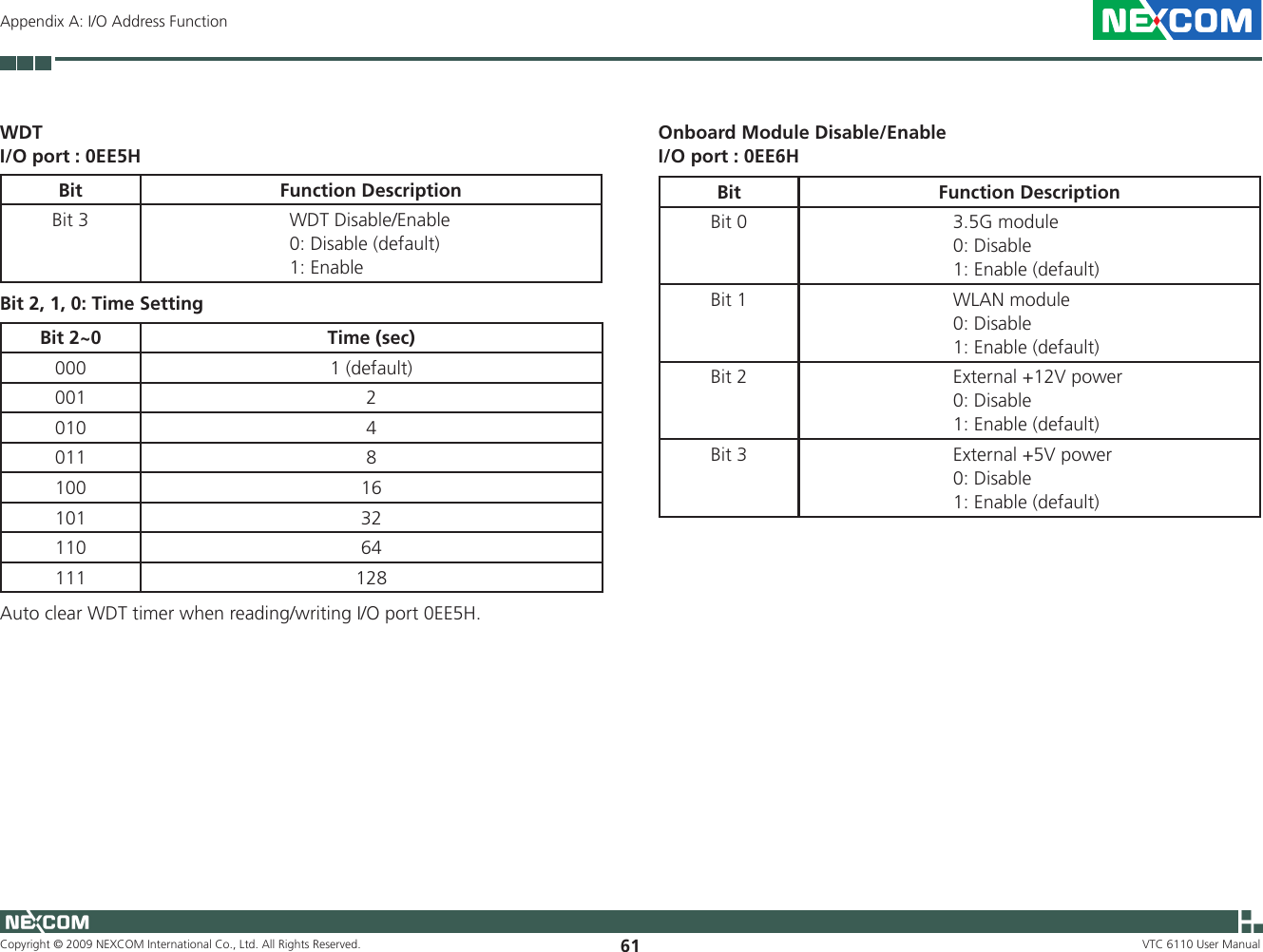
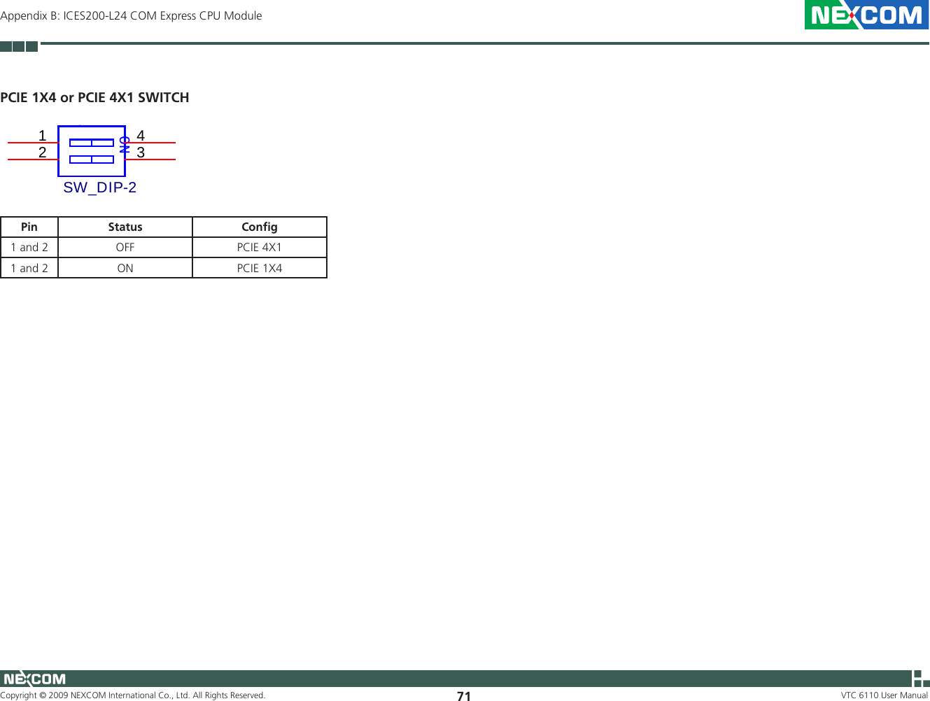
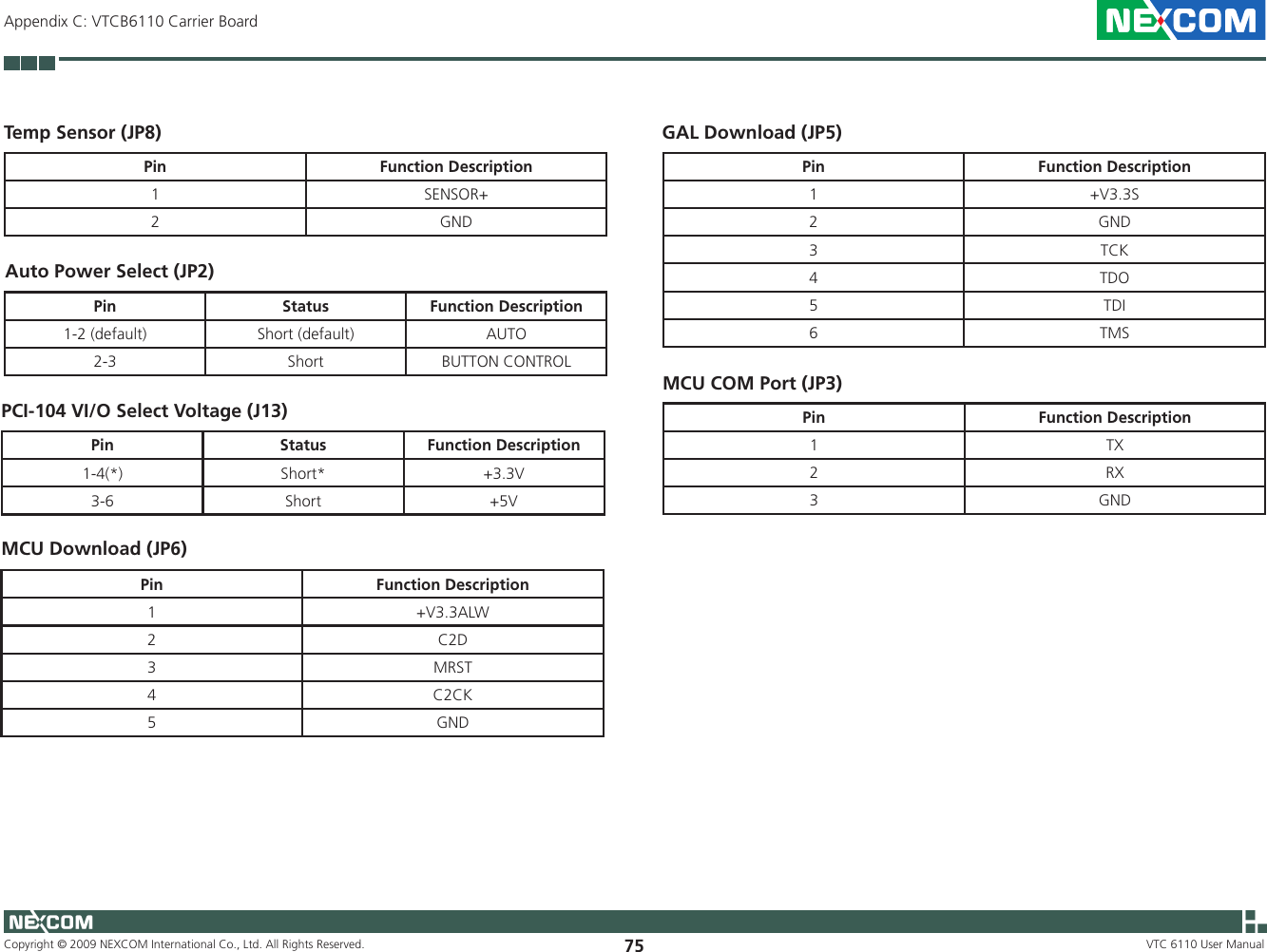
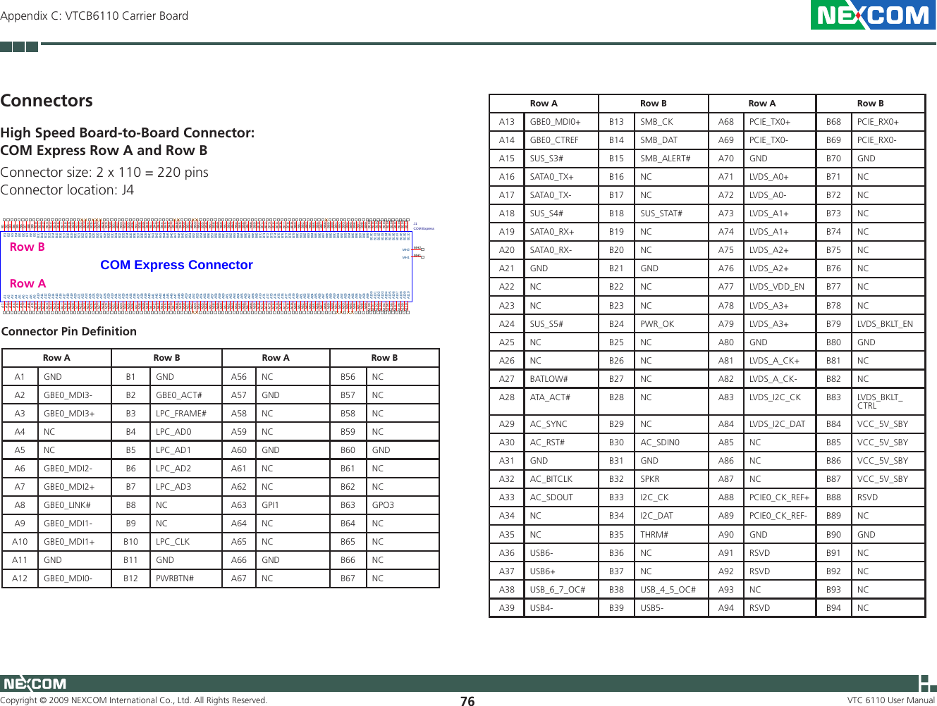
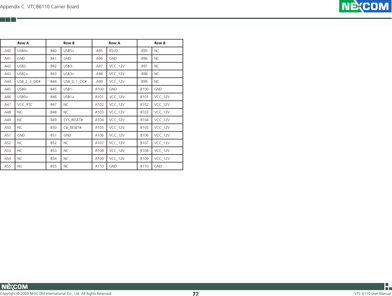
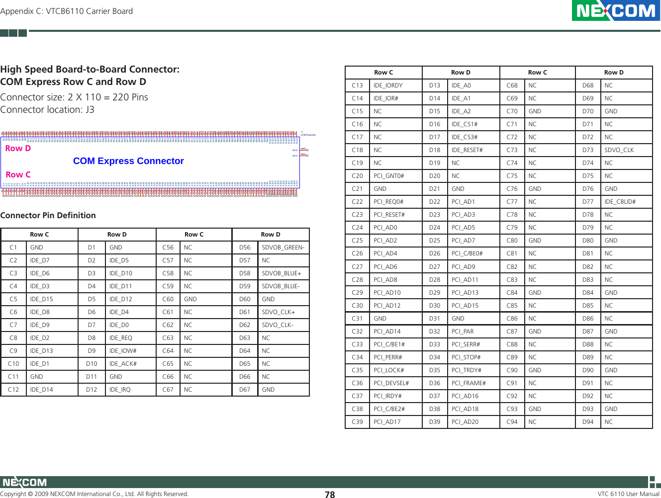
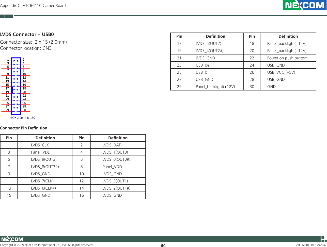
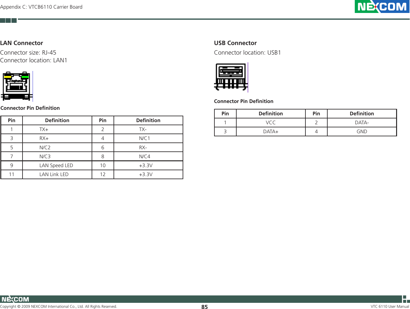
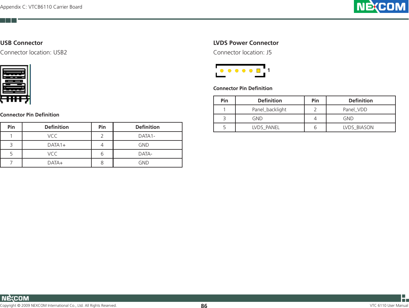
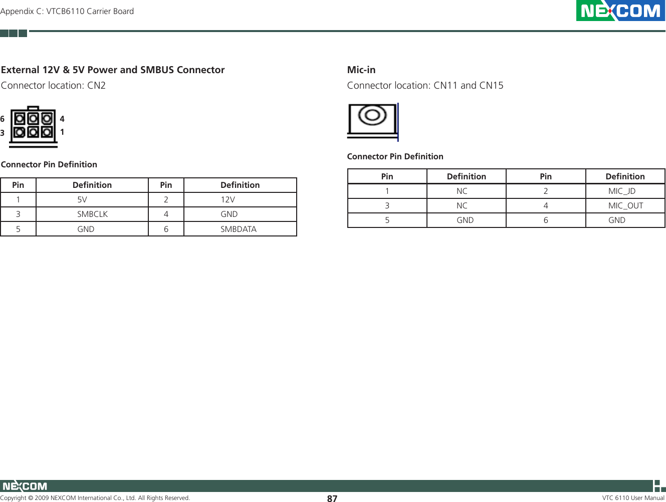
NEXCOM VTC6110X00 Intelligent Vehicle Telematics Computer User Manual 4

NEXCOM international Co.,LTD Intelligent Vehicle Telematics Computer 4

User manual4

Copyright © 2009 NEXCOM International Co., Ltd. All Rights Reserved. 57Chapter 3: System SetupVTC 6110 User ManualInstalling the USB Cable HolderThe USB cable holder is used to stabilize the USB cable so as to prevent it from getting loose when accidentally pulled or moved.1.  Attach the cable holder to the mounting hole by using the provided screw.2.  Hook the cable to the holder as shown in the photo below.Cable holder
Copyright © 2009 NEXCOM International Co., Ltd. All Rights Reserved. 58Chapter 3: System SetupVTC 6110 User Manual2.  Now mount the system on the wall by fastening screws through the bracket’s mounting holes.Fasten screws to mount the system to the wallRackmount BracketsThe rackmount brackets provide a convenient and economical way of mounting the system on the wall. 1.  The mounting holes are located at the bottom of the system. Secure the brackets on each side of the system using the provided mounting screws.Rackmount bracketSecure the bracket to the system
Copyright © 2009 NEXCOM International Co., Ltd. All Rights Reserved. 59 VTC 6110 User ManualAppendix A: I/O Address FunctionAp p e n d i x  A: i/O Ad d r e s s  Fu n c t i O nGPIO LED / UMTS LED / Ignition StatusI/O port : 0EE0HBit Function DescriptionBit 0 GPIO LED0: OFF (default)1: ONBit 1 UMTS LED 0: LED for WLAN (default)1: LED for 3.5G and WLAN Bit 2 Ignition (read only)0: OFF 1: ON Bit 3 Status of Vehicle Battery0: Vehicle Battery is OK 1: Vehicle Battery is Low VoltageBit0 Bit1 Bit2 Bit3 Bit4 Bit5 Bit6 Bit7Description 8 bits data (Bit 7 is highest bit of data)Capacity of NEXCOM battery (8 bits) I/O port : 0EE1HBit0 Bit1 Bit2 Bit3 Bit4 Bit5 Bit6 Bit7Description 8 bits data (Bit 7 is highest bit of data)Voltage of NEXCOM battery (8 bits) I/O port : 0EE2H
Copyright © 2009 NEXCOM International Co., Ltd. All Rights Reserved. 60 VTC 6110 User ManualAppendix A: I/O Address FunctionStatus of NEXCOM battery (8 bits)I/O port : 0EE3HBit Function DescriptionBit 0 Status for G sensor detection0: Normal1: Abnormal (X-axis or Y-axis degree is about 90 or -90)Bit 1 Power mode 0: 24V system1: 12V system Bit 2 Fan mode0: Auto 1: Always on Bit 3 Status of Smart battery0: No discharging 1: DischargingBit 4 Status of Fan R0: Well 1: FailedBit 5 Status of Fan R0: Action 1: InactionBit 6 Status of Fan L0: Well 1: FailedBit 7 Status of Fan L0: Action 1: InactionGPIOI/O port : 0EE4HBit Function DescriptionBit 0-3 GPO 1-4Bit 4-7 GPI 1-4
Copyright © 2009 NEXCOM International Co., Ltd. All Rights Reserved. 61 VTC 6110 User ManualAppendix A: I/O Address FunctionOnboard Module Disable/EnableI/O port : 0EE6HBit Function DescriptionBit 0                             3.5G module                            0: Disable                            1: Enable (default)Bit 1                             WLAN module                             0: Disable                            1: Enable (default) Bit 2                             External +12V power                            0: Disable                            1: Enable (default) Bit 3                             External +5V power                            0: Disable                            1: Enable (default)Bit 2, 1, 0: Time SettingBit 2~0 Time (sec)000 1 (default)001 2010 4011 8100 16101 32110 64111 128WDTI/O port : 0EE5HBit Function DescriptionBit 3                            WDT Disable/Enable                           0: Disable (default)                           1: EnableAuto clear WDT timer when reading/writing I/O port 0EE5H.
Copyright © 2009 NEXCOM International Co., Ltd. All Rights Reserved. 62 VTC 6110 User ManualAppendix B: ICES200-L24 COM Express CPU ModuleAp p e n d i x  B: iCeS200-L24 COM ex p r e S S  CpU MO d U L eOverviewICES 200 is a Type 2 COM Express Module that features Intel® 945GME and ICH7M chipset; switch supports Intel® Core™ 2 Duo and Intel® Core™ 2 Duo LV processors with 533/667 MHz FSB. One DDR2 memory socket supports up to 2GB. The ICES 200 is integrated with Intel® Graphics Media Accelerator (GMA950) and expands via PCI Express Graphics x16 lanes to the carrier board. It also supports other display interfaces including LFP or Dual channel LVDS.The high performance ICES 200 COM Express Module supports 2 x SATA, 8 x USB 2.0 and 4 PCIe x1 Lanes through the carrier board.Key FeaturesIntel• ® Socket M supports Core™ 2 Duo / Core™ 2 Duo LV Processor FamilyIntel• ® 945GME ChipsetOne DDR2 SO-DIMM socket supports un-buffered non-ECC DDR2 •533/667 up to 2GBSupports 2 x Serial ATA for high speed drives, 8 x USB 2.0 for fast pe-•ripheralsType 2 COM Express Module supports up to 21 Express lanes, 32 bit PCI •interface, one IDE and Gigabit LAN
Copyright © 2009 NEXCOM International Co., Ltd. All Rights Reserved. 63 VTC 6110 User ManualAppendix B: ICES200-L24 COM Express CPU ModuleDisplayIntegrated with Intel• ® Graphics Media Accelerator (GMA950) or expand via PCI Express Graphics x16 lanes / Dual SDVOCRT resolution up to 2048 x 1536 @ 60Hz, 1600 x 1200 @ 85Hz •One PCI Express x16 Lane down to the carrier board•Supports LFP (Local Flat Panel) LVDS interface with resolution up to 1366 •x 768Supports Single channel for 18 bit / Dual Channel for 18 bit•AudioHD audio interface•COM Express ConnectorsAB •  -  VGA / LVDS / 8 x USB 2.0 / HD Audio / 2 x SATA / LAN / GPIO / LPC bus / 1 x PCIe x4 / 1 x PCIe x1 / 5 x PCIe x1 / SMBus (I2C) / SPI BIOSCD •  -  PCIe x16 / IDE / PCISystem MonitorDerived from HW monitor •Monitors 4 voltages, 2 temperatures and 1 fan speed •4 voltages (For +3.3 V, +5 V, +12 V, Vcore)•2 temperatures (CPU and one external Temperature Sensor)•Power Requirements+ 12 V, + 5 VSB, + 3.3 V RTC•SpecificationsCPU SupportSupports Intel• ® Socket M, Core™ 2 Duo Family ProcessorsSupports 533/667MHz FSB CPU•Main Memory1 x DDR2 SO-DIMM socket•ChipsetIntel• ® 945GMEICH7M I/O Controller Hub•BIOSAward System BIOS •Plug & Play support•8Mbit Flash ROM•Onboard LANRealtek PCI Express GbE 8111C-GR•Supports PXE LAN boot function•Supports Wake on LAN•
Copyright © 2009 NEXCOM International Co., Ltd. All Rights Reserved. 64 VTC 6110 User ManualAppendix B: ICES200-L24 COM Express CPU ModuleDimensionsCOM Express Basic Module Type 2• 95mm x 125mm•
Copyright © 2009 NEXCOM International Co., Ltd. All Rights Reserved. 65 VTC 6110 User ManualAppendix B: ICES200-L24 COM Express CPU ModuleMechanical Dimensions
Copyright © 2009 NEXCOM International Co., Ltd. All Rights Reserved. 66 VTC 6110 User ManualAppendix B: ICES200-L24 COM Express CPU ModulePCI RoutingSlot / Device SignalSlot / Device 0 Slot / Device 1 Slot / Device 2 Slot / Device 3IDSEL AD20 AD21 AD22 AD23INTA# IRQA IRQB IRQC IRQDINTB# IRQB IRQC IRQD IRQAINTC# IRQC IRQD IRQA IRQBINTD# IRQD IRQA IRQB IRQCCOM Express Module Connector
Copyright © 2009 NEXCOM International Co., Ltd. All Rights Reserved. 67 VTC 6110 User ManualAppendix B: ICES200-L24 COM Express CPU ModuleConnectors High Speed Board-to-Board Connector: COM Express Row A and Row BConnector size: 2 X 110 = 220 PinsConnector location: J2Row BRow ACOM Express ConnectorJ1COM Express A1A1A2A2A3A3A4A4A5A5A6A6A7A7A8A8A9A9A10A10A11A11A12A12A13A13A14A14A15A15A16A16A17A17A18A18A19A19A20A20A21A21A22A22A23A23A24A24A25A25A26A26A27A27A28A28A29A29A30A30A31A31A32A32A33A33A34A34A35A35A36A36A37A37A38A38A39A39A40A40A41A41A42A42A43A43A44A44A45A45A46A46A47A47A48A48A49A49A50A50A51A51A52A52A53A53A54A54A55A55A56A56A57A57A58A58A59A59A60A60A61A61A62A62A63A63A64A64A65A65A66A66A67A67A68A68A69A69A70A70A71A71A72A72A73A73A74A74A75A75A76A76A77A77A78A78A79A79A80A80A81A81A82A82A83A83A84A84A85A85A86A86A87A87A88A88A89A89A90A90A91A91A92A92A93A93A94A94A95A95A96A96A97A97A98A98A99A99A100A100A101A101A102A102A103A103A104A104A105A105A106A106A107A107A108A108A109A109A110A110B1 B1B2 B2B3 B3B4 B4B5 B5B6 B6B7 B7B8 B8B9 B9B10 B10B11 B11B12 B12B13 B13B14 B14B15 B15B16 B16B17 B17B18 B18B19 B19B20 B20B21 B21B22 B22B23 B23B24 B24B25 B25B26 B26B27 B27B28 B28B29 B29B30 B30B31 B31B32 B32B33 B33B34 B34B35 B35B36 B36B37 B37B38 B38B39 B39B40 B40B41 B41B42 B42B43 B43B44 B44B45 B45B46 B46B47 B47B48 B48B49 B49B50 B50B51 B51B52 B52B53 B53B54 B54B55 B55B56 B56B57 B57B58 B58B59 B59B60 B60B61 B61B62 B62B63 B63B64 B64B65 B65B66 B66B67 B67B68 B68B69 B69B70 B70B71 B71B72 B72B73 B73B74 B74B75 B75B76 B76B77 B77B78 B78B79 B79B80 B80B81 B81B82 B82B83 B83B84 B84B85 B85B86 B86B87 B87B88 B88B89 B89B90 B90B91 B91B92 B92B93 B93B94 B94B95 B95B96 B96B97 B97B98 B98B99 B99B100 B100B101 B101B102 B102B103 B103B104 B104B105 B105B106 B106B107 B107B108 B108B109 B109B110 B110MH1 MH1MH2 MH2Connector Pin DefinitionRow A Row B Row A Row BA1  GND  B1  GND  A56 PCIE_TX4- B56 PCIE_RX4-A2  GBE0_MDI3-  B2  GBE0_ACT#  A57 GND B57 GPO2A3  GBE0_MDI3+  B3  LPC_FRAME#  A58 PCIE_TX3+ B58 PCIE_RX3+A4  GBE0_LINK100#  B4  LPC_AD0  A59 PCIE_TX3- B59 PCIE_RX3-A5  GBE0_LINK1000#  B5  LPC_AD1  A60 GND  B60 GND A6  GBE0_MDI2-  B6  LPC_AD2  A61 PCIE_TX2+ B61 PCIE_RX2+A7  GBE0_MDI2+  B7  LPC_AD3  A62 PCIE_TX2- B62 PCIE_RX2-A8  GBE0_LINK#  B8  LPC_DRQ0#  A63 GPI1 B63 GPO3A9  GBE0_MDI1-  B9  LPC_DRQ1#  A64 PCIE_TX1+ B64 PCIE_RX1+A10  GBE0_MDI1+  B10  LPC_CLK  A65 PCIE_TX1- B65 PCIE_RX1-A11  GND  B11  GND  A66 GND B66 WAKE0#A12  GBE0_MDI0-  B12  PWRBTN#  A67 GPI2 B67 WAKE1#Row A Row B Row A Row BA13  GBE0_MDI0+  B13  SMB_CK  A68 PCIE_TX0+ B68 PCIE_RX0+A14  GBE0_CTREF  B14  SMB_DAT  A69 PCIE_TX0- B69 PCIE_RX0-A15  SUS_S3#  B15  SMB_ALERT#  A70 GND  B70 GND A16  SATA0_TX+  B16  SATA1_TX+  A71 LVDS_A0+ B71 LVDS_B0+A17  SATA0_TX-  B17  SATA1_TX-  A72 LVDS_A0- B72 LVDS_B0-A18  SUS_S4#  B18  SUS_STAT#  A73 LVDS_A1+ B73 LVDS_B1+A19  SATA0_RX+  B19  SATA1_RX+  A74 LVDS_A1+ B74 LVDS_B1-A20  SATA0_RX-  B20  SATA1_RX-  A75 LVDS_A2+ B75 LVDS_B2+A21  GND  B21  GND  A76 LVDS_A2+ B76 LVDS_B2-A22  NC B22  NC A77 LVDS_VDD_EN B77 LVDS_B3+A23  NC B23  NC A78 LVDS_A3+ B78 LVDS_B3-A24  SUS_S5#  B24  PWR_OK  A79 LVDS_A3+ B79 LVDS_BKLT_ENA25  NC  B25  NC A80 GND  B80 GND A26  NC B26  NC A81 LVDS_A_CK+ B81 LVDS_B_CK+A27  BATLOW#  B27  NC A82 LVDS_A_CK- B82 LVDS_B_CK-A28  ATA_ACT#  B28  AC_SDIN2  A83 LVDS_I2C_CK B83 LVDS_BKLT_CTRLA29  AC_SYNC  B29  AC_SDIN1  A84 LVDS_I2C_DAT B84 VCC_5V_SBYA30  AC_RST#  B30  AC_SDIN0  A85  GPI3  B85  VCC_5V_SBY A31  GND  B31  GND  A86  KBD_RST#  B86  VCC_5V_SBY A32  AC_BITCLK  B32  SPKR  A87  KBD_A20GATE  B87  VCC_5V_SBY A33  AC_SDOUT  B33  I2C_CK  A88  PCIE0_CK_REF+  B88  RSVD A34  BIOS_DISABLE#  B34  I2C_DAT  A89  PCIE0_CK_REF-  B89  VGA_RED A35  THRMTRIP#  B35  THRM#  A90  GND  B90  GND A36  USB6-  B36  USB7-  A91  RSVD  B91  VGA_GRN A37  USB6+  B37  USB7+  A92  RSVD  B92  VGA_BLU A38  USB_6_7_OC#  B38  USB_4_5_OC#  A93  GPO0  B93  VGA_HSYNC A39  USB4-  B39  USB5-  A94  RSVD  B94  VGA_VSYNC
Copyright © 2009 NEXCOM International Co., Ltd. All Rights Reserved. 68 VTC 6110 User ManualAppendix B: ICES200-L24 COM Express CPU ModuleRow A Row B Row A Row BA40  USB4+  B40  USB5+  A95  RSVD  B95  VGA_I2C_CK A41  GND  B41  GND  A96  GND  B96  VGA_I2C_DAT A42  USB2-  B42  USB3-  A97  VCC_12V  B97  NCA43  USB2+  B43  USB3+  A98  VCC_12V  B98  NCA44  USB_2_3_OC#  B44  USB_0_1_OC#  A99  VCC_12V  B99  NCA45  USB0-  B45  USB1-  A100  GND  B100  GND A46  USB0+  B46  USB1+  A101 VCC_12V B101 VCC_12VA47  VCC_RTC  B47  NC  A102 VCC_12V B102 VCC_12VA48  EXCD0_PERST#  B48  NC  A103 VCC_12V B103 VCC_12VA49  EXCD0_CPPE#  B49  SYS_RESET#  A104 VCC_12V B104 VCC_12VA50  LPC_SERIRQ  B50  CB_RESET#  A105 VCC_12V B105 VCC_12VA51 GND  B51 GND  A106 VCC_12V B106 VCC_12VA52 NC B52 NC A107 VCC_12V B107 VCC_12VA53 NC B53 NC A108 VCC_12V B108 VCC_12VA54 GPI0 B54 GPO1 A109 VCC_12V B109 VCC_12VA55 PCIE_TX4+ B55 PCIE_RX4+ A110  GND  B110  GND
Copyright © 2009 NEXCOM International Co., Ltd. All Rights Reserved. 69 VTC 6110 User ManualAppendix B: ICES200-L24 COM Express CPU ModuleHigh Speed Board-to-Board Connector: COM Express Row C and Row DConnector size: 2 X 110 = 220 PinsConnector location: J1COM Express ConnectorJ1COM Express A1A1A2A2A3A3A4A4A5A5A6A6A7A7A8A8A9A9A10A10A11A11A12A12A13A13A14A14A15A15A16A16A17A17A18A18A19A19A20A20A21A21A22A22A23A23A24A24A25A25A26A26A27A27A28A28A29A29A30A30A31A31A32A32A33A33A34A34A35A35A36A36A37A37A38A38A39A39A40A40A41A41A42A42A43A43A44A44A45A45A46A46A47A47A48A48A49A49A50A50A51A51A52A52A53A53A54A54A55A55A56A56A57A57A58A58A59A59A60A60A61A61A62A62A63A63A64A64A65A65A66A66A67A67A68A68A69A69A70A70A71A71A72A72A73A73A74A74A75A75A76A76A77A77A78A78A79A79A80A80A81A81A82A82A83A83A84A84A85A85A86A86A87A87A88A88A89A89A90A90A91A91A92A92A93A93A94A94A95A95A96A96A97A97A98A98A99A99A100A100A101A101A102A102A103A103A104A104A105A105A106A106A107A107A108A108A109A109A110A110B1 B1B2 B2B3 B3B4 B4B5 B5B6 B6B7 B7B8 B8B9 B9B10 B10B11 B11B12 B12B13 B13B14 B14B15 B15B16 B16B17 B17B18 B18B19 B19B20 B20B21 B21B22 B22B23 B23B24 B24B25 B25B26 B26B27 B27B28 B28B29 B29B30 B30B31 B31B32 B32B33 B33B34 B34B35 B35B36 B36B37 B37B38 B38B39 B39B40 B40B41 B41B42 B42B43 B43B44 B44B45 B45B46 B46B47 B47B48 B48B49 B49B50 B50B51 B51B52 B52B53 B53B54 B54B55 B55B56 B56B57 B57B58 B58B59 B59B60 B60B61 B61B62 B62B63 B63B64 B64B65 B65B66 B66B67 B67B68 B68B69 B69B70 B70B71 B71B72 B72B73 B73B74 B74B75 B75B76 B76B77 B77B78 B78B79 B79B80 B80B81 B81B82 B82B83 B83B84 B84B85 B85B86 B86B87 B87B88 B88B89 B89B90 B90B91 B91B92 B92B93 B93B94 B94B95 B95B96 B96B97 B97B98 B98B99 B99B100 B100B101 B101B102 B102B103 B103B104 B104B105 B105B106 B106B107 B107B108 B108B109 B109B110 B110MH1 MH1MH2 MH2Row DRow CConnector Pin DefinitionRow C Row D Row C Row DC1  GND  D1  GND  C56 PEG_RX1- D56 PEG_TX1-C2  IDE_D7  D2  IDE_D5  C57 TYPE1# D57 TYPE2#C3  IDE_D6  D3  IDE_D10  C58 PEG_RX2+ D58 PEG_TX2+C4  IDE_D3  D4  IDE_D11  C59 PEG_RX2- D59 PEG_TX2-C5  IDE_D15  D5  IDE_D12  C60 GND  D60 GND C6  IDE_D8  D6  IDE_D4  C61 PEG_RX3+ D61 PEG_TX3+C7  IDE_D9  D7  IDE_D0  C62 PEG_RX3- D62 PEG_TX3-C8  IDE_D2  D8  IDE_REQ  C63 RSVD D63 RSVDC9  IDE_D13  D9  IDE_IOW#  C64 RSVD D64 RSVDC10  IDE_D1  D10  IDE_ACK#  C65 PEG_RX4+ D65 PEG_TX4+C11  GND  D11  GND  C66 PEG_RX4- D66 PEG_TX4-C12  IDE_D14  D12  IDE_IRQ  C67 RSVD D67 GNDRow C Row D Row C Row DC13  IDE_IORDY  D13  IDE_A0  C68 PEG_RX5+ D68 PEG_TX5+C14  IDE_IOR#  D14  IDE_A1  C69 PEG_RX5- D69 PEG_TX5-C15  PCI_PME#  D15  IDE_A2  C70 GND  D70 GND C16  PCI_GNT2#  D16  IDE_CS1#  C71 PEG_RX6+ D71 PEG_TX6+C17  PCI_REQ2#  D17  IDE_CS3#  C72 PEG_RX6- D72 PEG_TX6-C18  PCI_GNT1#  D18  IDE_RESET#  C73 SDVO_DATA D73 SDVO_CLKC19  PCI_REQ1#  D19  PCI_GNT3#  C74 PEG_RX7+ D74 PEG_TX7+C20  PCI_GNT0#  D20  PCI_REQ3#  C75 PEG_RX7- D75 PEG_TX7-C21  GND  D21  GND  C76 GND D76 GNDC22  PCI_REQ0#  D22  PCI_AD1  C77 RSVD D77 IDE_CBLID#C23  PCI_RESET#  D23  PCI_AD3  C78 PEG_RX8+ D78 PEG_TX8+C24  PCI_AD0  D24  PCI_AD5  C79 PEG_RX8- D79 PEG_TX8-C25  PCI_AD2  D25  PCI_AD7  C80 GND  D80 GND C26  PCI_AD4  D26  PCI_C/BE0#  C81 PEG_RX9+ D81 PEG_TX9+C27  PCI_AD6  D27  PCI_AD9  C82 PEG_RX9- D82 PEG_TX9-C28  PCI_AD8  D28  PCI_AD11  C83 RSVD D83 RSVDC29  PCI_AD10  D29  PCI_AD13  C84 GND D84 GNDC30  PCI_AD12  D30  PCI_AD15  C85  PEG_RX10+  D85  PEG_TX10+ C31  GND  D31  GND  C86  PEG_RX10-  D86  PEG_TX10- C32  PCI_AD14  D32  PCI_PAR  C87  GND  D87  GND C33  PCI_C/BE1#  D33  PCI_SERR#  C88  PEG_RX11+  D88  PEG_TX11+ C34  PCI_PERR#  D34  PCI_STOP#  C89  PEG_RX11-  D89  PEG_TX11- C35  PCI_LOCK#  D35  PCI_TRDY#  C90  GND  D90  GND C36  PCI_DEVSEL#  D36  PCI_FRAME#  C91  PEG_RX12+  D91  PEG_TX12+ C37  PCI_IRDY#  D37  PCI_AD16  C92  PEG_RX12-  D92  PEG_TX12- C38  PCI_C/BE2#  D38  PCI_AD18  C93  GND  D93  GND C39  PCI_AD17  D39  PCI_AD20  C94  PEG_RX13+  D94  PEG_TX13+
Copyright © 2009 NEXCOM International Co., Ltd. All Rights Reserved. 70 VTC 6110 User ManualAppendix B: ICES200-L24 COM Express CPU ModuleRow C Row D Row C Row DC40  PCI_AD19  D40  PCI_AD22  C95  PEG_RX13-  D95  PEG_TX13- C41  GND  D41  GND  C96  GND D96  GNDC42  PCI_AD21  D42  PCI_AD24  C97  RSVD  D97  PEG_ENABLE# C43  PCI_AD23  D43  PCI_AD26  C98  PEG_RX14+  D98  PEG_TX14+ C44  PCI_C/BE3#  D44  PCI_AD28  C99  PEG_RX14-  D99  PEG_TX14- C45  PCI_AD25  D45  PCI_AD30  C100  GND  D100  GND C46  PCI_AD27  D46  PCI_IRQC#  C101 PEG_RX15+ D101 PEG_TX15+C47  PCI_AD29  D47  PCI_IRQD#  C102 PEG_RX15- D102 PEG_TX15-C48  PCI_AD31  D48  PCI_CLKRUN#  C103 GND D103 GNDC49  PCI_IRQA#  D49  PCI_M66EN  C104 VCC_12V D104 VCC_12VC50  PCI_IRQB#  D50  PCI_CLK  C105 VCC_12V D105 VCC_12VC51 GND  D51 GND  C106 VCC_12V D106 VCC_12VC52 PEG_RX0+ D52 PEG_TX0+ C107 VCC_12V D107 VCC_12VC53 PEG_RX0- D53 PEG_TX0- C108 VCC_12V D108 VCC_12VC54 TYPE0# D54 PEG_LANE_RV# C109 VCC_12V D109 VCC_12VC55 PEG_RX1+ D55 PEG_TX1+ C110  GND  D110  GND
Copyright © 2009 NEXCOM International Co., Ltd. All Rights Reserved. 71 VTC 6110 User ManualAppendix B: ICES200-L24 COM Express CPU ModulePCIE 1X4 or PCIE 4X1 SWITCHONSW1SW_DIP-212 34Pin Status Config1 and 2 OFF PCIE 4X11 and 2 ON PCIE 1X4
Copyright © 2009 NEXCOM International Co., Ltd. All Rights Reserved. 72 VTC 6110 User ManualAppendix C: VTCB6110 Carrier BoardAp p e n d i x  C: VTCB6110 CA r r i e r  Bo A r dSpecificationsExpansion1 PCI-104 socket•1 Bluetooth module (optional)•2 Mini PCI Express socket•  - 1 PCIe interface for WLAN module  - 1 PCIe + USB interface for 3.5G moduleStorageOne SATA 2.5” HDD bay •One internal Type I/ II CompactFlash socket•I/O Interfaces - Front4 SMA-type mounting holes for WLAN, HSDPA and Bluetooth•1 power button•1 reset switch•1 SIM card socket•1 USB 2.0•4 LEDs for Standby, HDD, WLAN/HSDPA and GPO•1 line-out•1 mic-in•I/O Interfaces - Front4 SMA-type mounting holes for WLAN, HSDPA and Bluetooth•1 power button•1 reset switch•1 SIM card socket•1 USB 2.0•4 LEDs for Standby, HDD, WLAN/HSDPA and GPO•1 line-out•1 mic-in•Dimensions260mm(W) x 176mm(D) x 50mm(H) •  10.24”(W) x 7”(D) x 1.97”(H)
Copyright © 2009 NEXCOM International Co., Ltd. All Rights Reserved. 73Appendix C: VTCB6110 Carrier BoardVTC 6110 User ManualJumpers and ConnectorsCN4CN1710 1J14CN11CN216J5COM1302921CN3CON1J861CN51 4J10SW61 7CN612910CN71910CN912910CN12USB2LAN11151751216185211517512161852CN161J12CN84CN111CN1426CN1552162921135BZ1241261JP551JP621JP821JP7J71013131J631JP431JP331JP231JP131J1SW1J3J4LED1LED2USB1SW7SW2SW3SW4SW51J111J21J941Blue ToothWLAN3.5GJ13
Copyright © 2009 NEXCOM International Co., Ltd. All Rights Reserved. 74Appendix C: VTCB6110 Carrier BoardVTC 6110 User ManualJumper SettingsSW5 / Input Voltage12V (default) 24V 6V~36VSW5.1 OFF OFF ONSW5.2 OFF ON IgnoreSW5: Input Voltage SelectionSW6: COM Port Mode SelectionSW6 COM Port Mode RS232 (default)RS485SW6.1 OFF ONSW6.2 OFF ONSW6.3 OFF ONCF (IDE0) Primary Master/Slave Select (JP4)Pin  Status Function Description1-2 Short Slave2-3 (default) Short (default) MasterLVDS Power Input Voltage Select (JP9)Pin  Status Function Description1-2 Short +5V IN2-3 (default) Short (default) +3.3V INCMOS Input Voltage Select (J6)Pin  Status Function Description1-2 (default) Short (default) VBAT IN2-3 Short Clear CMOSBIOS Function Select (J1)Pin Status Function Description1-2 Short Disable carrier board BIOS2-3 (default) Short (default) Disable module board BIOSDC Input Voltage Select (JP1)Pin Status Function Description1-2 (default) Short (default) IGNITION2-3 Short VIN_M
Copyright © 2009 NEXCOM International Co., Ltd. All Rights Reserved. 75Appendix C: VTCB6110 Carrier BoardVTC 6110 User ManualTemp Sensor (JP8)Pin Function Description1 SENSOR+2 GNDAuto Power Select (JP2)Pin Status Function Description1-2 (default) Short (default) AUTO2-3 Short BUTTON CONTROLPCI-104 VI/O Select Voltage (J13)Pin Status Function Description1-4(*) Short* +3.3V3-6 Short +5VMCU Download (JP6)Pin Function Description1 +V3.3ALW2 C2D3 MRST4 C2CK5 GNDGAL Download (JP5)Pin Function Description1 +V3.3S2 GND3 TCK4 TDO5 TDI6 TMSMCU COM Port (JP3)Pin Function Description1 TX2 RX3 GND
Copyright © 2009 NEXCOM International Co., Ltd. All Rights Reserved. 76Appendix C: VTCB6110 Carrier BoardVTC 6110 User ManualConnectorsHigh Speed Board-to-Board Connector: COM Express Row A and Row BConnector size: 2 x 110 = 220 pinsConnector location: J4COM Express ConnectorJ1COM Express A1A1A2A2A3A3A4A4A5A5A6A6A7A7A8A8A9A9A10A10A11A11A12A12A13A13A14A14A15A15A16A16A17A17A18A18A19A19A20A20A21A21A22A22A23A23A24A24A25A25A26A26A27A27A28A28A29A29A30A30A31A31A32A32A33A33A34A34A35A35A36A36A37A37A38A38A39A39A40A40A41A41A42A42A43A43A44A44A45A45A46A46A47A47A48A48A49A49A50A50A51A51A52A52A53A53A54A54A55A55A56A56A57A57A58A58A59A59A60A60A61A61A62A62A63A63A64A64A65A65A66A66A67A67A68A68A69A69A70A70A71A71A72A72A73A73A74A74A75A75A76A76A77A77A78A78A79A79A80A80A81A81A82A82A83A83A84A84A85A85A86A86A87A87A88A88A89A89A90A90A91A91A92A92A93A93A94A94A95A95A96A96A97A97A98A98A99A99A100A100A101A101A102A102A103A103A104A104A105A105A106A106A107A107A108A108A109A109A110A110B1 B1B2 B2B3 B3B4 B4B5 B5B6 B6B7 B7B8 B8B9 B9B10 B10B11 B11B12 B12B13 B13B14 B14B15 B15B16 B16B17 B17B18 B18B19 B19B20 B20B21 B21B22 B22B23 B23B24 B24B25 B25B26 B26B27 B27B28 B28B29 B29B30 B30B31 B31B32 B32B33 B33B34 B34B35 B35B36 B36B37 B37B38 B38B39 B39B40 B40B41 B41B42 B42B43 B43B44 B44B45 B45B46 B46B47 B47B48 B48B49 B49B50 B50B51 B51B52 B52B53 B53B54 B54B55 B55B56 B56B57 B57B58 B58B59 B59B60 B60B61 B61B62 B62B63 B63B64 B64B65 B65B66 B66B67 B67B68 B68B69 B69B70 B70B71 B71B72 B72B73 B73B74 B74B75 B75B76 B76B77 B77B78 B78B79 B79B80 B80B81 B81B82 B82B83 B83B84 B84B85 B85B86 B86B87 B87B88 B88B89 B89B90 B90B91 B91B92 B92B93 B93B94 B94B95 B95B96 B96B97 B97B98 B98B99 B99B100 B100B101 B101B102 B102B103 B103B104 B104B105 B105B106 B106B107 B107B108 B108B109 B109B110 B110MH1 MH1MH2 MH2Connector Pin DefinitionRow A Row B Row A Row BA1  GND  B1  GND  A56 NC B56 NCA2  GBE0_MDI3-  B2  GBE0_ACT#  A57 GND B57 NCA3  GBE0_MDI3+  B3  LPC_FRAME#  A58 NC B58 NCA4  NC B4  LPC_AD0  A59 NC B59 NCA5  NC B5  LPC_AD1  A60 GND  B60 GND A6  GBE0_MDI2-  B6  LPC_AD2  A61 NC B61 NCA7  GBE0_MDI2+  B7  LPC_AD3  A62 NC B62 NCA8  GBE0_LINK#  B8  NC A63 GPI1 B63 GPO3A9  GBE0_MDI1-  B9  NC A64 NC B64 NCA10  GBE0_MDI1+  B10  LPC_CLK  A65 NC B65 NCA11  GND  B11  GND  A66 GND B66 NCA12  GBE0_MDI0-  B12  PWRBTN#  A67 NC B67 NCRow A Row B Row A Row BA13  GBE0_MDI0+  B13  SMB_CK  A68 PCIE_TX0+ B68 PCIE_RX0+A14  GBE0_CTREF  B14  SMB_DAT  A69 PCIE_TX0- B69 PCIE_RX0-A15  SUS_S3#  B15  SMB_ALERT#  A70 GND  B70 GND A16  SATA0_TX+  B16  NC  A71 LVDS_A0+ B71 NCA17  SATA0_TX-  B17  NC  A72 LVDS_A0- B72 NCA18  SUS_S4#  B18  SUS_STAT#  A73 LVDS_A1+ B73 NCA19  SATA0_RX+  B19  NC  A74 LVDS_A1+ B74 NCA20  SATA0_RX-  B20  NC  A75 LVDS_A2+ B75 NCA21  GND  B21  GND  A76 LVDS_A2+ B76 NCA22  NC B22  NC A77 LVDS_VDD_EN B77 NCA23  NC B23  NC A78 LVDS_A3+ B78 NCA24  SUS_S5#  B24  PWR_OK  A79 LVDS_A3+ B79 LVDS_BKLT_ENA25  NC  B25  NC A80 GND  B80 GND A26  NC B26  NC A81 LVDS_A_CK+ B81 NCA27  BATLOW#  B27  NC A82 LVDS_A_CK- B82 NCA28  ATA_ACT#  B28  NC  A83 LVDS_I2C_CK B83 LVDS_BKLT_CTRLA29  AC_SYNC  B29  NC A84 LVDS_I2C_DAT B84 VCC_5V_SBYA30  AC_RST#  B30  AC_SDIN0  A85  NC  B85  VCC_5V_SBY A31  GND  B31  GND  A86  NC B86  VCC_5V_SBY A32  AC_BITCLK  B32  SPKR  A87  NC B87  VCC_5V_SBYA33  AC_SDOUT  B33  I2C_CK  A88  PCIE0_CK_REF+  B88  RSVD A34  NC  B34  I2C_DAT  A89  PCIE0_CK_REF-  B89  NC A35  NC  B35  THRM#  A90  GND  B90  GND A36  USB6-  B36  NC A91  RSVD  B91  NC A37  USB6+  B37  NC  A92  RSVD  B92  NC A38  USB_6_7_OC#  B38  USB_4_5_OC#  A93  NC B93  NC A39  USB4-  B39  USB5-  A94  RSVD  B94  NC Row BRow A
Copyright © 2009 NEXCOM International Co., Ltd. All Rights Reserved. 77Appendix C: VTCB6110 Carrier BoardVTC 6110 User ManualRow A Row B Row A Row BA40  USB4+  B40  USB5+  A95  RSVD  B95  NC A41  GND  B41  GND  A96  GND  B96  NC A42  USB2-  B42  USB3-  A97  VCC_12V  B97  NCA43  USB2+  B43  USB3+  A98  VCC_12V  B98  NCA44  USB_2_3_OC#  B44  USB_0_1_OC#  A99  VCC_12V  B99  NCA45  USB0-  B45  USB1-  A100  GND  B100  GND A46  USB0+  B46  USB1+  A101 VCC_12V B101 VCC_12VA47  VCC_RTC  B47  NC  A102 VCC_12V B102 VCC_12VA48  NC B48  NC  A103 VCC_12V B103 VCC_12VA49  NC  B49  SYS_RESET#  A104 VCC_12V B104 VCC_12VA50  NC  B50  CB_RESET#  A105 VCC_12V B105 VCC_12VA51 GND  B51 GND  A106 VCC_12V B106 VCC_12VA52 NC B52 NC A107 VCC_12V B107 VCC_12VA53 NC B53 NC A108 VCC_12V B108 VCC_12VA54 NC  B54 NC A109 VCC_12V B109 VCC_12VA55 NC B55 NC A110  GND  B110  GND
Copyright © 2009 NEXCOM International Co., Ltd. All Rights Reserved. 78Appendix C: VTCB6110 Carrier BoardVTC 6110 User ManualHigh Speed Board-to-Board Connector: COM Express Row C and Row DConnector size: 2 X 110 = 220 PinsConnector location: J3COM Express ConnectorJ1COM Express A1A1A2A2A3A3A4A4A5A5A6A6A7A7A8A8A9A9A10A10A11A11A12A12A13A13A14A14A15A15A16A16A17A17A18A18A19A19A20A20A21A21A22A22A23A23A24A24A25A25A26A26A27A27A28A28A29A29A30A30A31A31A32A32A33A33A34A34A35A35A36A36A37A37A38A38A39A39A40A40A41A41A42A42A43A43A44A44A45A45A46A46A47A47A48A48A49A49A50A50A51A51A52A52A53A53A54A54A55A55A56A56A57A57A58A58A59A59A60A60A61A61A62A62A63A63A64A64A65A65A66A66A67A67A68A68A69A69A70A70A71A71A72A72A73A73A74A74A75A75A76A76A77A77A78A78A79A79A80A80A81A81A82A82A83A83A84A84A85A85A86A86A87A87A88A88A89A89A90A90A91A91A92A92A93A93A94A94A95A95A96A96A97A97A98A98A99A99A100A100A101A101A102A102A103A103A104A104A105A105A106A106A107A107A108A108A109A109A110A110B1 B1B2 B2B3 B3B4 B4B5 B5B6 B6B7 B7B8 B8B9 B9B10 B10B11 B11B12 B12B13 B13B14 B14B15 B15B16 B16B17 B17B18 B18B19 B19B20 B20B21 B21B22 B22B23 B23B24 B24B25 B25B26 B26B27 B27B28 B28B29 B29B30 B30B31 B31B32 B32B33 B33B34 B34B35 B35B36 B36B37 B37B38 B38B39 B39B40 B40B41 B41B42 B42B43 B43B44 B44B45 B45B46 B46B47 B47B48 B48B49 B49B50 B50B51 B51B52 B52B53 B53B54 B54B55 B55B56 B56B57 B57B58 B58B59 B59B60 B60B61 B61B62 B62B63 B63B64 B64B65 B65B66 B66B67 B67B68 B68B69 B69B70 B70B71 B71B72 B72B73 B73B74 B74B75 B75B76 B76B77 B77B78 B78B79 B79B80 B80B81 B81B82 B82B83 B83B84 B84B85 B85B86 B86B87 B87B88 B88B89 B89B90 B90B91 B91B92 B92B93 B93B94 B94B95 B95B96 B96B97 B97B98 B98B99 B99B100 B100B101 B101B102 B102B103 B103B104 B104B105 B105B106 B106B107 B107B108 B108B109 B109B110 B110MH1 MH1MH2 MH2Row DRow CConnector Pin DefinitionRow C Row D Row C Row DC1  GND  D1  GND  C56 NC D56 SDVOB_GREEN-C2  IDE_D7  D2  IDE_D5  C57 NC D57 NCC3  IDE_D6  D3  IDE_D10  C58 NC D58 SDVOB_BLUE+C4  IDE_D3  D4  IDE_D11  C59 NC D59 SDVOB_BLUE-C5  IDE_D15  D5  IDE_D12  C60 GND  D60 GND C6  IDE_D8  D6  IDE_D4  C61 NC D61 SDVO_CLK+C7  IDE_D9  D7  IDE_D0  C62 NC D62 SDVO_CLK-C8  IDE_D2  D8  IDE_REQ  C63 NC D63 NCC9  IDE_D13  D9  IDE_IOW#  C64 NC D64 NCC10  IDE_D1  D10  IDE_ACK#  C65 NC D65 NCC11  GND  D11  GND  C66 NC D66 NCC12  IDE_D14  D12  IDE_IRQ  C67 NC D67 GNDRow C Row D Row C Row DC13  IDE_IORDY  D13  IDE_A0  C68 NC D68 NCC14  IDE_IOR#  D14  IDE_A1  C69 NC D69 NCC15  NC D15  IDE_A2  C70 GND  D70 GND C16  NC  D16  IDE_CS1#  C71 NC D71 NCC17  NC D17  IDE_CS3#  C72 NC D72 NCC18  NC  D18  IDE_RESET#  C73 NC D73 SDVO_CLKC19  NC  D19  NC  C74 NC D74 NCC20  PCI_GNT0#  D20  NC C75 NC D75 NCC21  GND  D21  GND  C76 GND D76 GNDC22  PCI_REQ0#  D22  PCI_AD1  C77 NC D77 IDE_CBLID#C23  PCI_RESET#  D23  PCI_AD3  C78 NC D78 NCC24  PCI_AD0  D24  PCI_AD5  C79 NC D79 NCC25  PCI_AD2  D25  PCI_AD7  C80 GND  D80 GND C26  PCI_AD4  D26  PCI_C/BE0#  C81 NC D81 NCC27  PCI_AD6  D27  PCI_AD9  C82 NC D82 NCC28  PCI_AD8  D28  PCI_AD11  C83 NC D83 NCC29  PCI_AD10  D29  PCI_AD13  C84 GND D84 GNDC30  PCI_AD12  D30  PCI_AD15  C85  NC  D85  NC C31  GND  D31  GND  C86  NC  D86  NC C32  PCI_AD14  D32  PCI_PAR  C87  GND  D87  GND C33  PCI_C/BE1#  D33  PCI_SERR#  C88  NC  D88  NC C34  PCI_PERR#  D34  PCI_STOP#  C89  NC  D89  NCC35  PCI_LOCK#  D35  PCI_TRDY#  C90  GND  D90  GND C36  PCI_DEVSEL#  D36  PCI_FRAME#  C91  NC  D91  NCC37  PCI_IRDY#  D37  PCI_AD16  C92  NC D92  NCC38  PCI_C/BE2#  D38  PCI_AD18  C93  GND  D93  GND C39  PCI_AD17  D39  PCI_AD20  C94  NC  D94  NC
Copyright © 2009 NEXCOM International Co., Ltd. All Rights Reserved. 79Appendix C: VTCB6110 Carrier BoardVTC 6110 User ManualRow C Row D Row C Row DC40  PCI_AD19  D40  PCI_AD22  C95  PEG_RX13-  D95  PEG_TX13- C41  GND  D41  GND  C96  GND D96  GNDC42  PCI_AD21  D42  PCI_AD24  C97  RSVD  D97  PEG_ENABLE# C43  PCI_AD23  D43  PCI_AD26  C98  PEG_RX14+  D98  PEG_TX14+ C44  PCI_C/BE3#  D44  PCI_AD28  C99  PEG_RX14-  D99  PEG_TX14- C45  PCI_AD25  D45  PCI_AD30  C100  GND  D100  GND C46  PCI_AD27  D46  PCI_IRQC#  C101 PEG_RX15+ D101 PEG_TX15+C47  PCI_AD29  D47  PCI_IRQD#  C102 PEG_RX15- D102 PEG_TX15-C48  PCI_AD31  D48  PCI_CLKRUN#  C103 GND D103 GNDC49  PCI_IRQA#  D49  PCI_M66EN  C104 VCC_12V D104 VCC_12VC50  PCI_IRQB#  D50  PCI_CLK  C105 VCC_12V D105 VCC_12VC51 GND  D51 GND  C106 VCC_12V D106 VCC_12VC52 PEG_RX0+ D52 PEG_TX0+ C107 VCC_12V D107 VCC_12VC53 PEG_RX0- D53 PEG_TX0- C108 VCC_12V D108 VCC_12VC54 TYPE0# D54 PEG_LANE_RV# C109 VCC_12V D109 VCC_12VC55 PEG_RX1+ D55 PEG_TX1+ C110  GND  D110  GND
Copyright © 2009 NEXCOM International Co., Ltd. All Rights Reserved. 80Appendix C: VTCB6110 Carrier BoardVTC 6110 User ManualCompactFlash Connector Connector size: 2 x 25 = 50 pinsConnector location: J12 1 26 50 49 Pin Description Pin Description1            Gnd 2           Data 33            Data 4 4           Data 55            Data 6 6           Data 77            HDC CS100 8           Gnd9            Gnd 10           Gnd11            Gnd 12           Gnd13            +5V 14           Gnd15            Gnd 16           Gnd17            Gnd 18           Disk Address 219            Disk Address 1 20           Disk Address 021            Data 0 22           Data 1Connector Pin DefinitionPin Description Pin Description23  Data 2 24 IOCS16# (NC)25  CF_CD2# (Pull-down) 26 CF_CD1# (Pull-down)27  Data 11 28 Data 1229  Data 13 30 Data 1431  Data 15 32 HDC CS30033  CF_VS1# (NC) 34 IOR35  IOW 36 CF_WE# (+5V)37  Interrupt 15 38 +5V39  CF_CSEL# (Master or Slave) 40 CF_VS2# (NC)41  Reset # 42 IOCHRDY43  DMA REQ / DACK (NC) 44 DMA ACK# /CF_REG# (+5V)45  HDD Active Led 46 DMA66 Detect / CF_PDIAG#47  Data 8 48 Data 949  Data 10 50 Gnd
Copyright © 2009 NEXCOM International Co., Ltd. All Rights Reserved. 81Appendix C: VTCB6110 Carrier BoardVTC 6110 User ManualGPIO Connector Connector size: DSUB-9 pinConnector location: COM1Pin Description Pin  Description1                GIN1 2                GIN2 3                GIN3 4                GIN4 5                GOUT4 6                GOUT17                GOUT2 8                GOUT39                GNDConnector Pin Definition5 19 6RS232 Connector: COM1, COM2Connector size: 2 x 10 = 20 Pins Pin Header, (2.0 mm Pitch)Connector location: COM1 (CN9), COM2 (CN7)CN10BOX-2.0mm-M-18013 425 67 8910Connector Pin DefinitionPin Definition Pin Definition1 DCD 2 RXD 3 TXD 4 DTR 5 Gnd 6 DSR 7 RTS  8 CTS 9 RI
Copyright © 2009 NEXCOM International Co., Ltd. All Rights Reserved. 82Appendix C: VTCB6110 Carrier BoardVTC 6110 User ManualRS232/485 Connector: COM3Connector size: 2 x 10 = 20 Pins Pin Header, (2.0 mm Pitch)Connector location: CN12CN10BOX-2.0mm-M-18013 425 67 8910Connector Pin DefinitionPin Definition Pin Definition1           DCD (RS232)          TX-/RX- (RS485)2         RXD (RS232)        TX+/RX+ (RS485)3           TXD (RS232) 4         DTR (RS232)5           Gnd 6         DSR (RS232)7           RTS (RS232) 8         CTS (RS232)9           RI (RS232)GAL Programmer PIN Header Connector size: 2.54mm-M-180Connector location: JP5JP5PIN-2.54mm-M-180123456Connector Pin DefinitionPin Definition Pin Definition1 +3.3V 2 GND3 TCK 4 TDO5 TDI 6 TMS
Copyright © 2009 NEXCOM International Co., Ltd. All Rights Reserved. 83Appendix C: VTCB6110 Carrier BoardVTC 6110 User ManualMCU Programmer Pin Header Connector size: 2.54mm-M-180Connector location: JP6JP6PIN-2.54mm-M-18012345Connector Pin DefinitionPin Definition Pin Definition  1     +3.3ALW 2 C2D  3    MRST 4 C2CK  5     GNDVGA Connector Connector size: DSUB-15Connector location: CON1Connector Pin DefinitionPin Definition Pin Definition1               RED 2                GREEN 3               BLUE 4                NC5               Gnd 6                Gnd7               Gnd 8                Gnd9               VCC 10                Gnd11               NC 12                DDCDAT13               Hsync 14                Vsync15               DDCCLK
Copyright © 2009 NEXCOM International Co., Ltd. All Rights Reserved. 84Appendix C: VTCB6110 Carrier BoardVTC 6110 User ManualLVDS Connector + USB0Connector size:  2 x 15 (2.0mm)Connector location: CN3CN3BOX-2.0mm-M-18013 425 67 8911 101213 14161517 18202224262830212325272919Connector Pin DefinitionPin Definition Pin Definition1           LVDS_CLK 2          LVDS_DAT3           Panel_VDD 4          LVDS_1(OUT0)5           LVDS_9(OUT3) 6          LVDS_0(OUT0#)7           LVDS_8(OUT3#) 8          Panel_VDD9           LVDS_GND 10          LVDS_GND11           LVDS_7(CLK) 12          LVDS_3(OUT1)13           LVDS_6(CLK#) 14          LVDS_2(OUT1#)15           LVDS_GND 16          LVDS_GNDPin Definition Pin Definition17      LVDS_5(OUT2) 18     Panel_backlight(+12V)19      LVDS_4(OUT2#) 20     Panel_backlight(+12V)21      LVDS_GND 22     Power on push buttom23      USB_0# 24     USB_GND25      USB_0 26     USB_VCC (+5V)27      USB_GND 28     USB_GND29      Panel_backlight(+12V) 30     GND
Copyright © 2009 NEXCOM International Co., Ltd. All Rights Reserved. 85Appendix C: VTCB6110 Carrier BoardVTC 6110 User ManualLAN Connector Connector size: RJ-45Connector location: LAN1Connector Pin DefinitionPin Definition Pin Definition1           TX+ 2                 TX-3           RX+ 4                 N/C15           N/C2 6                 RX-7           N/C3 8                 N/C49           LAN Speed LED 10                 +3.3V11           LAN Link LED 12                 +3.3VUSB Connector Connector location: USB1Connector Pin DefinitionPin Definition Pin Definition1 VCC 2 DATA-3 DATA+ 4 GND
Copyright © 2009 NEXCOM International Co., Ltd. All Rights Reserved. 86Appendix C: VTCB6110 Carrier BoardVTC 6110 User ManualConnector Pin DefinitionPin Definition Pin Definition1                 VCC 2                 DATA1-3                 DATA1+ 4                 GND5                 VCC 6                 DATA-7                 DATA+ 8                 GNDUSB Connector Connector location: USB2LVDS Power Connector Connector location: J51Connector Pin DefinitionPin Definition Pin Definition1           Panel_backlight 2           Panel_VDD3           GND 4           GND5           LVDS_PANEL 6           LVDS_BIASON
Copyright © 2009 NEXCOM International Co., Ltd. All Rights Reserved. 87Appendix C: VTCB6110 Carrier BoardVTC 6110 User ManualExternal 12V & 5V Power and SMBUS Connector Connector location: CN26341Connector Pin DefinitionPin Definition Pin Definition1                 5V 2               12V3                 SMBCLK 4               GND5                 GND 6               SMBDATAMic-in Connector location: CN11 and CN15Connector Pin DefinitionPin Definition Pin Definition1            NC 2         MIC_JD3            NC 4         MIC_OUT5            GND 6         GND
Copyright © 2009 NEXCOM International Co., Ltd. All Rights Reserved. 88Appendix C: VTCB6110 Carrier BoardVTC 6110 User ManualLine-out Connector location: CN8 and CN14Connector Pin DefinitionPin Definition Pin Definition1              LINE_OUT_L 2             SURR_JD3              NC 4             LINE_OUT_R5              GND 6             GNDPCI-104 VI/O Voltage Setting Connector location: J13Connector Pin DefinitionPin No. Status Function Description         1-3, 2-4 (default) Short                 +3.3V         3-5, 4-6 Short                 +5V4 623 51
Copyright © 2009 NEXCOM International Co., Ltd. All Rights Reserved. 89Appendix C: VTCB6110 Carrier BoardVTC 6110 User ManualPCI-104 Connector Connector location: CN16Connector Pin DefinitionPower Button Connector location: SW1Reset Button Connector location: SW2
Copyright © 2009 NEXCOM International Co., Ltd. All Rights Reserved. 90Appendix C: VTCB6110 Carrier BoardVTC 6110 User ManualMCU COM Port Connector location: JP3Connector Pin DefinitionPin Function Description1 TX2 RX3 GNDACC_ON LED Connector location: JP71Connector Pin DefinitionPin Function Description1               +3.3V LED2               GND
Copyright © 2009 NEXCOM International Co., Ltd. All Rights Reserved. 91Appendix C: VTCB6110 Carrier BoardVTC 6110 User ManualTemp Sensor Connector location: JP81Connector Pin DefinitionPin Function Description1                SENSOR+2                GNDDC Power Input Connector Connector location: CN1Connector Pin DefinitionPin Function Description1            GND2            VIN (6V~36V)3            IGNITION
Copyright © 2009 NEXCOM International Co., Ltd. All Rights Reserved. 92Appendix C: VTCB6110 Carrier BoardVTC 6110 User ManualPower On and IDE Active LED Connector location: LED1T1B1Connector Pin DefinitionLED Function DescriptionT1              POWER LEDB1              HD LEDGPIO and UMTS LEDs Connector location: LED2T2B2LED I/O Port Address and DataLED Function DescriptionT2    I/O PORT Address: 0EE0; Bit0: 1 (Light), 0 (Dark)B2    UMTS STATUS
Copyright © 2009 NEXCOM International Co., Ltd. All Rights Reserved. 93Appendix C: VTCB6110 Carrier BoardVTC 6110 User ManualSerial ATA Connector location: CN617Connector Pin DefinitionPin Definition Pin Definition1              GND 2              SATA_TXP0 -3              SATA_TXN0 4              GND5              SATA_RXN0 6              SATA_RXP07              GNDSerial ATA Power Input Connector location: J1014Connector Pin DefinitionPin Definition Pin Definition1 +V12S 2 GND3 GND 4 +V5S
Copyright © 2009 NEXCOM International Co., Ltd. All Rights Reserved. 94Appendix C: VTCB6110 Carrier BoardVTC 6110 User ManualMini-PCIe Socket (for 3.5G module) PCIe InterfaceConnector location: CN10 125152Connector Pin DefinitionPin Definition Pin Definition Pin Definition Pin Definition1 MIC + 2 +V3.3S 27 GND 28 NC3 MIC - 4 GND 29 GND 30 NC5 SPK + 6 NC 31 NC 32 NC7 GND 8 USIM PWR 33 RESET 34 GND9 GND 10 USIM DATa 35 GND 36 USB_D-11 VCC_    MSM26_DIG12 USIM CLK 37 GND 38 USB_D+13 NC 14 USIM RST 39 +V3.3S 40 GND15 GND 16 NC 41 +V3.3S 42 LED_WWAN#17 NC 18 GND 43 GND 44 NC19 NC 20 W_DIS-ABLE#45 NC 46 NC21 GND 22 NC 47 NC 48 NC23 NC 24 NC 49 NC 50 GND25 NC 26 GND 51 NC 52 +V3.3SMini-PCIe Socket (for WLAN module) USB + PCIe InterfaceConnector location: CN13 125152Connector Pin DefinitionPin Definition Pin Definition Pin Definition Pin Definition1 WAKE# 2 +V3.3S 27 GND 28 +V1.5S3 NC 4 GND 29 GND 30 SMB_CLK5 NC 6 +V1.5S 31 PETn0 32 SMB_DATA7 CLKREQ# 8 NC 33 PETp0 34 GND9 GND 10 NC 35 GND 36 USB_D-11 REFCLK- 12 NC 37 NC 38 USB_D+13 REFCLK+ 14 NC 39 NC 40 GND15 GND 16 NC 41 NC 42 LED_WWAN#17 NC 18 GND 43 NC 44 LED_WLAN#19 NC 20 DISABLE# 45 NC 46 LED_WPAN#21 GND 22 PERST# 47 NC 48 +V1.5S23 PERn0 24 +3.3S 49 NC 50 GND25 PERp0 26 GND 51 NC 52 +V3.3S
Copyright © 2009 NEXCOM International Co., Ltd. All Rights Reserved. 95Appendix C: VTCB6110 Carrier BoardVTC 6110 User ManualSIM Card Connector Connector location: CN4Connector Pin DefinitionPin Definition Pin DefinitionC1    POWER VOLTAGE C2            RESET SIGNALC3    CLOCK SIGNAL C5            GNDC6    VPP:PROGRAM VOLTAGE C7            I/OSW    Contact present switchBluetooth Connector Connector location: J7J7JST-1mm-M-90123MH1MH245610987 Pin Definition Pin Definition1              GND 2         USB_6P_L3              USB_6N_L 4         NC5              NC 6         BT_AUDIO_EN_R7              NC 8         BT_3.3V9              NC 10         GND
Copyright © 2009 NEXCOM International Co., Ltd. All Rights Reserved. 96 VTC 6110 User ManualAppendix D: BIOS SetupAp p e n d i x  d: Ve h i c l e  po w e r  MA n A g e M e n t  Se t u pExternal Power Output SettingExternal +12V and +5V Turn On SimultaneouslyExternal +12V and +5V Turn Off Simultaneously
Copyright © 2009 NEXCOM International Co., Ltd. All Rights Reserved. 97 VTC 6110 User ManualAppendix D: BIOS SetupExternal +12V Turn On Only External +5V Turn On Only
Copyright © 2009 NEXCOM International Co., Ltd. All Rights Reserved. 98 VTC 6110 User ManualAppendix D: BIOS SetupStartup and Shutdown Voltage Setting1. If the input voltage setting is 12V: set the startup voltage to 11.5V and the shutdown voltage to 10.5V.   If the input voltage setting is 24V: set the startup voltage to 23V and the shutdown voltage to 21V.   If the input voltage setting is 6V~36V, ignore the startup/shutdown set-ting.2. If the input voltage setting is 12V: set the startup voltage to 12V and the shutdown voltage to 11V.    If the input voltage setting is 24V: set the startup voltage to 24V and the shutdown voltage to 22V.    If the input voltage setting is 6V~36V, ignore the startup/shutdown set-ting.
Copyright © 2009 NEXCOM International Co., Ltd. All Rights Reserved. 99 VTC 6110 User ManualAppendix D: BIOS Setup3. If the input voltage setting is 12V: set the startup voltage to 12.5V and the shutdown voltage to 11V.   If the input voltage setting is 24V: set the startup voltage to 25V and the shutdown voltage to 22V.   If the input voltage setting is 6V~36V, ignore the startup/shutdown set-ting.4. If the input voltage setting is 12V: set the startup voltage to 12.5V and the shutdown voltage to 11.5V.    If input voltage setting is 24V: set the startup voltage to 25V and the shutdown voltage to 23V.    If the input voltage setting is 6V~36V ignore the startup/shutdown set-ting.
Copyright © 2009 NEXCOM International Co., Ltd. All Rights Reserved. 100 VTC 6110 User ManualAppendix D: BIOS SetupPower-on Delay SettingDisable Power-on DelayEnable Power-on DelayDelay time can be set at 10sec/30sec/1min./5min./10min./15min./30min./1hour.
Copyright © 2009 NEXCOM International Co., Ltd. All Rights Reserved. 101 VTC 6110 User ManualAppendix D: BIOS SetupPower-off Delay SettingDisable Power-off Delay
Copyright © 2009 NEXCOM International Co., Ltd. All Rights Reserved. 102 VTC 6110 User ManualAppendix D: BIOS SetupEnable Power-off DelayDelay time can be set at 20sec/1min./5min./10min./30min./1hour/6hour/ 18hour.
For mobile devices without co-location condition ( the transmitting antenna is installed or located more than 20cm away from the body of user and near by person ) FCC RF Radiation Exposure Statement: 1. This Transmitter must not be co-located or operating in conjunction with any other antenna or transmitter. 2. This equipment complies with FCC RF radiation exposure limits set forth for an uncontrolled environment. This equipment should be installed and operated with a minimum distance of 20 centimeters between the radiator and your body. This equipment has been tested and found to comply with the limits for a Class B digital device, pursuant to part 15 of the FCC rules. These limits are designed to provide reasonable protection against harmful interference in a residential installation. This equipment generates, uses and can radiate radio frequency energy and, if not installed and used in accordance with the instructions, may cause harmful interference to radio communications. However, there is no guarantee that interference will not occur in a particular installation. If this equipment does cause harmful interference to radio or television reception, which can be determined by turning the equipment off and on, the user is encouraged to try to correct the interference by one or more of the following measures: -Reorient or relocate the receiving antenna. -Increase the separation between the equipment and receiver. -Connect the equipment into an outlet on a circuit different from that to which the receiver is connected. -Consult the dealer or an experienced radio/TV technician for help. You are cautioned that changes or modifications not expressly approved by the party responsible for compliance could void your authority to operate the equipment. This device complies with Part 15 of the FCC Rules. Operation is subject to the following two conditions: (1) this device may not cause harmful interference and (2) this device must accept any interference received, including interference that may cause undesired operation

Navigation menu