NXP Laboratories UK JN5139M0 IEEE 802.15.4 Wireless Microcontroller User Manual JN DS JN5139MO 1v5
NXP Laboratories UK Ltd IEEE 802.15.4 Wireless Microcontroller JN DS JN5139MO 1v5
Contents
- 1. Manual
- 2. Module data sheet
- 3. manual
- 4. Revised Datasheet
Revised Datasheet
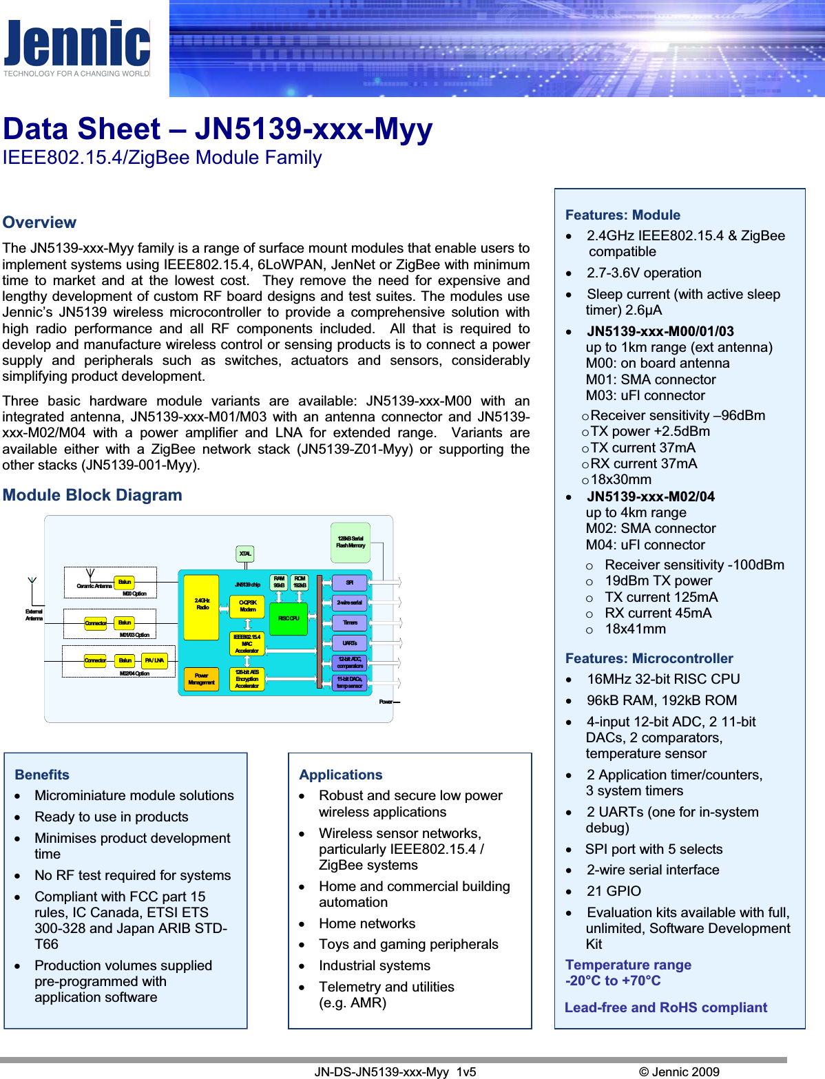
![Jennic © Jennic 2009 JN-DS-JN5139-xxx-Myy 1v5 3 1. Introduction The JN5139-xxx-Myy module family provides designers with a ready made component which allows IEEE802.15.4 [1] wireless applications, using Jennic’s JenNet networking protocol or ZigBee, to be quickly and easily included in product designs. The modules integrate all of the RF components required, removing the need to perform expensive RF design and test. Products can be designed by simply connecting sensors and switches to the module IO pins. The modules use Jennic’s single chip IEEE802.15.4 Wireless Microcontroller, allowing designers to make use of the extensive chip development support material. Hence, this range of modules allows designers to bring wireless applications to market in the minimum time with significantly reduced development effort and cost. Three module hardware variants are available: JN5139-xxx-M00 (standard module with on board ceramic antenna), JN5139-xxx-M01 (standard module with SMA connector for use with external antennae – recommended for evaluation use) and JN5139-xxx-M02 (high RF power, improved sensitivity module for evaluation of extended range applications). For volume production applications, uFL connector variants are provided (-M03 standard power and –M04 high power). These devices, together with the –M00 variants have FCC modular approvals. Each of these modules can be supplied with a range of protocol stacks, including JenNet for most tree and linear networks, IEEE802.15.4 protocol for point-to-point and star applications and a ZigBee mesh networking stack. The variants available are described below. 1.1. Variants 1.2. Regulatory Approvals All module types have been tested against the requirements of European standard ETS 300 328 v1.7.1 and a Notified Body statement of opinion for this standard is available on request. The High Power modules with M02 or M04 suffix are approved for use in Europe with reduced output power: +10dBm EIRP is the maximum permitted in Europe. They must not be used with PHY_PIB_ATTR_TX_POWER set above 50 See [3] JN-RM-2002 802.15.4 Stack API. Additionally, modules with M00, M03 and M04 suffixes have received FCC “Modular Approvals”, in compliance with CFR 47 FCC part 15 regulations and in accordance to FCC Public notice DA00-1407. The modules are approved for use with a number of antennase, refer to section A.6.1 for details. See Appendix A.6 for details on the conditions applying to this modular approval. The modular approvals notice and test reports are available on request. The high power module variant is classified as ‘mobile’ device pursuant with FCC § 2.1091 and must not be used at a distance of less than 20 cm (8”) from any person. In addition, all modules have Industry Canada RSS 210 Issue 7 (June 2007) certification. Variant Description FCCID Industry Canada ID JN5139-001-M00 IEEE802.15.4 stack, ceramic antenna TYOJN5139M0 IC: 7438A-CYO5139M0 JN5139-Z01-M00 ZigBee stack, ceramic antenna TYOJN5139M0 IC: 7438A-CYO5139M0 JN5139-001-M01 IEEE802.15.4 stack, SMA connector - for evaluation N/A IC: 7438A-CYO5139M6 JN5139-Z01-M01 ZigBee stack, SMA connector – for evaluation N/A IC: 7438A-CYO5139M6 JN5139-001-M02 High Power, IEEE802.15.4 stack, SMA connector – for evaluation N/A IC: 7438A-CYO5139M4 JN5139-Z01-M02 High Power, ZigBee stack, SMA connector – for evaluation N/A IC: 7438A-CYO5139M4 JN5139-001-M03 IEEE802.15.4 stack, uFl connector TYOJN5139M3 IC: 7438A-CYO5139M6 JN5139-Z01-M03 ZigBee stack, uFl connector TYOJN5139M3 IC: 7438A-CYO5139M6 JN5139-001-M04 High Power, IEEE802.15.4 stack, uFl connector TYOJN5139M4 IC: 7438A-CYO5139M4 JN5139-Z01-M04 High Power, ZigBee stack, uFl connector TYOJN5139M4 IC: 7438A-CYO5139M4](https://usermanual.wiki/NXP-Laboratories-UK/JN5139M0.Revised-Datasheet/User-Guide-1088699-Page-3.png)
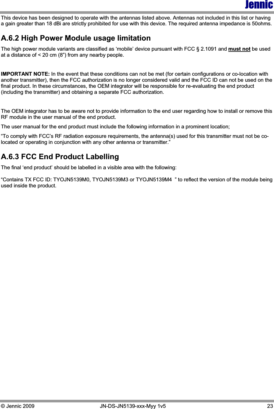
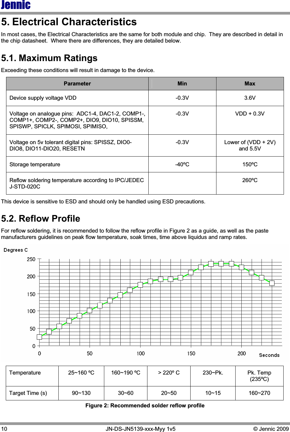
![Jennic4 JN-DS-JN5139-xxx-Myy 1v5 © Jennic 2009 2. Specifications Most specification parameters for the modules are specified in the chip datasheet - JN-DS- JN513x Wireless Microcontroller Datasheet, [2]. Where there are differences, the parameters are defined here. VDD=3.0V @ +25°CTypical DC Characteristics Notes JN5139-xxx-M00/01/03 JN5139-xxx- M02/04 Deep sleep current 1.3uA 1.3uA Sleep current 2.6uA 2.6uA With active sleep timer Radio transmit current 37mA 125mA CPU in doze, radio transmitting Radio receive current 37mA 45mA CPU in doze, radio receiving Centre frequency accuracy +/-25ppm +/-25ppm Additional +/-15ppm allowance for temperature and ageing Typical RF Characteristics Notes Receive sensitivity -96dBm -102dBm Nominal for 1% PER, as per 802.15.4 section 6.5.3.3 (Note 1) Maximum Transmit power +1dBm 17.5dBm Nominal (Note 1) Maximum Transmit power [Boost Mode] +2.5dBm N/A (Note 1) Transmit power at 3.6V 19dBm With Vdd=3.6V Maximum input signal +10dBm +10dBm For 1% PER, measured as sensitivity RSSI range -95 to -10 dBm-105 to -20 dBm RF Port impedance – SMA/uFl connector 50 ohm 50 ohm 2.4 - 2.5GHz VSWR (max) 2:1 2:1 2.4 - 2.5GHz Peripherals Notes Master SPI port 5 selects 3 selects 250kHz - 16MHz Slave SPI port 99250kHz - 8MHz Two UARTs 9916550 compatible Two-wire serial I/F (compatible with SMbus & I2C) 99Up to 400kHz Two programmable Timer/Counters with capture/compare facility, Tick timer 9916MHz clock Two programmable Sleep Timers 9932kHz clock Digital IO lines (multiplexed with UARTs, timers and SPI selects) 21 19 Four channel Analogue-to-Digital converter 9912-bit, up to 100ks/s Two channel Digital-to-Analogue converter 9911-bit, up to 100ks/s Two programmable analogue comparators 99Ultra low power mode for sleep Internal temperature sensor and battery monitor 99](https://usermanual.wiki/NXP-Laboratories-UK/JN5139M0.Revised-Datasheet/User-Guide-1088699-Page-4.png)
![Jennic © Jennic 2009 JN-DS-JN5139-xxx-Myy 1v5 5 The performance of all peripherals is defined in the JN-DS- JN513x Wireless Microcontroller Datasheet [2] Note 1: Sensitivity is defined for conducted measurements on connectorised modules. Modules with an integrated antenna have approximately 4 dB less e.i.r.p and reciprocal receive sensitivity.](https://usermanual.wiki/NXP-Laboratories-UK/JN5139M0.Revised-Datasheet/User-Guide-1088699-Page-5.png)
![Jennic6 JN-DS-JN5139-xxx-Myy 1v5 © Jennic 2009 3. Product Development Jennic supplies all the development tools and networking stacks needed to enable end product development to occur quickly and efficiently. These are all freely available from Jennic’s support website: http://www.jennic.com/support/ . A range of evaluation/developer kits is also available, allowing products to be quickly breadboarded. Efficient development of software applications is enabled by the provision of a complete, unlimited, software developer kit. Together with the available libraries for the JenNet networking stack, the IEEE802.15.4 MAC and the ZigBee network stack, this package provides everything required to develop application code and to trial it with hardware representative of the final module. The modules can be user programmed both in development and in production using software supplied by Jennic. They can also be supplied ready loaded with customer defined software if required. Access to the on-chip peripherals, MAC and network stack software is provided through specific APIs. This information is available on the Jennic support website, together with many example applications, user guides, reference manuals and application notes. 3.1. JN5139 Single Chip Wireless Microcontroller The JN5139-xxx-Myy series is constructed around the JN5139 single chip wireless microcontroller, which includes the radio system, a 32-bit RISC CPU, ROM and RAM memory and a range of analogue and digital peripherals. The chip is described fully in JN-DS- JN513x Wireless Microcontroller Datasheet [2]. The module also includes a 1Mbit serial flash memory which holds the application code that is loaded into the JN5139 during the boot sequence.](https://usermanual.wiki/NXP-Laboratories-UK/JN5139M0.Revised-Datasheet/User-Guide-1088699-Page-6.png)
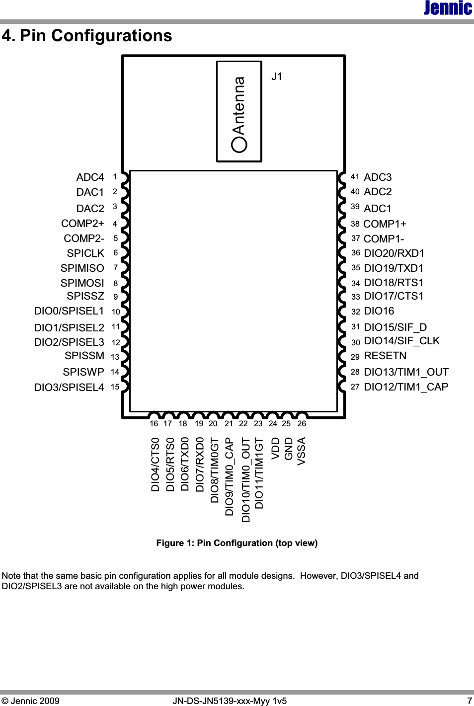
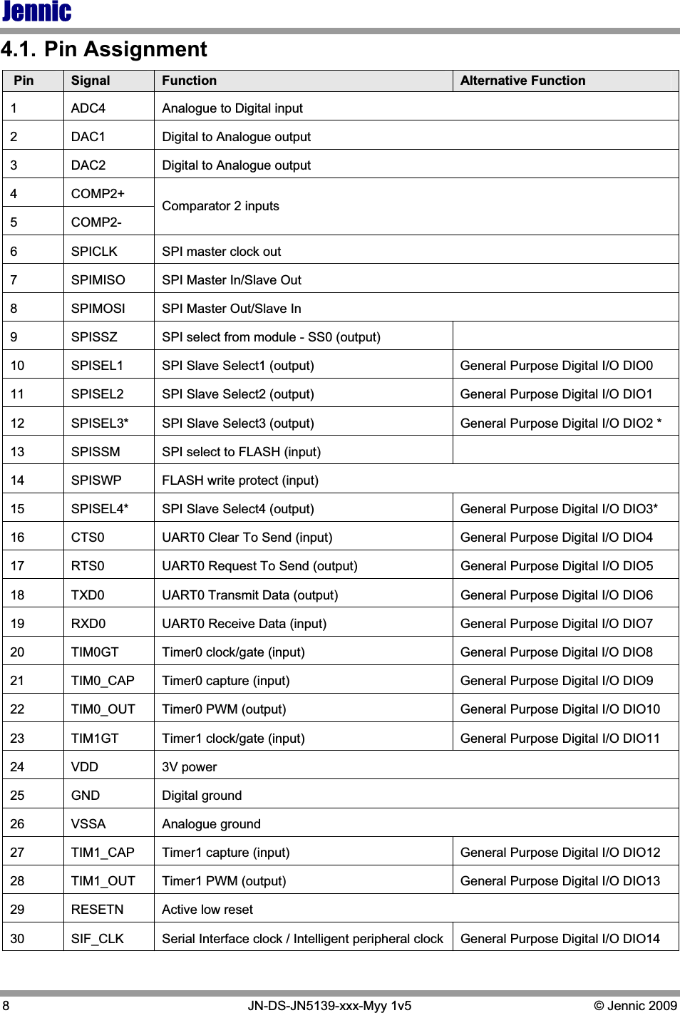
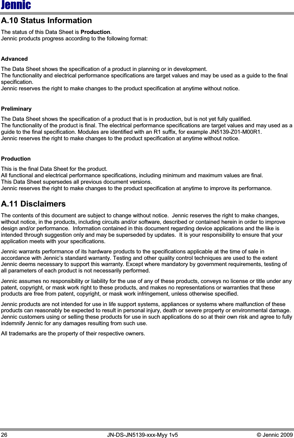
![Jennic © Jennic 2009 JN-DS-JN5139-xxx-Myy 1v5 9 Pin Signal Function Alternative Function 31 SIF_D Serial Interface data / Intelligent peripheral data out (output) General Purpose Digital I/O DIO15 32 DIO 16 Intelligent peripheral device data in (input) General Purpose Digital I/O 33 CTS1 UART1 Clear To Send (input) / Intelligent peripheral device select (input) General Purpose Digital I/O DIO17 34a RTS1 UART1 Request To Send (output) / Intelligent peripheral interrupt (output) General Purpose Digital I/O DIO18 35 TXD1 UART1 Transmit Data (output) General Purpose Digital I/O DIO19 36 RXD1 UART1 Receive Data (input) General Purpose Digital I/O DIO20 37 COMP1- 38 COMP1+ Comparator 1 inputs 39 ADC1 Analogue to Digital input 40 ADC2 Analogue to Digital input 41 ADC3 Analogue to Digital input *: These two pins are not connected for High power modules 4.2. Pin Descriptions All pins behave as described in the JN-DS- JN513x Wireless Microcontroller Datasheet [2], with the exception of the following: 4.2.1 Power Supplies A single power supply pin, VDD is provided. Separate analogue (VSSA) and digital (GND) grounds are provided. These should be connected together at the module pins. 4.2.2 SPI Memory Connections SPISWP is a write protect pin for the serial flash memory. This should be held low to inhibit writes to the flash device. SPISSZ is connected to SPI Slave Select 0 on the JN5139. SPISSM is connected to the Slave Select pin on the memory. This configuration allows the flash memory device to be programmed using an external SPI programmer if required. For programming in this mode, the JN5139 should be held in reset by taking RESETN low. The memory can also be programmed over the UART by using the flash programmer software provided by Jennic. This is available as part of the Software Developer kit and libraries available from Jennic’s support website – www.jennic.com/support. To enter this programming mode, SPIMISO (pin 7) should be held low whilst the chip is reset. Once programming has finished, the chip should be reset, when it will execute the new code downloaded. For normal operation of the module and programming over the UART, SPISSZ should be connected to SPISSM.](https://usermanual.wiki/NXP-Laboratories-UK/JN5139M0.Revised-Datasheet/User-Guide-1088699-Page-9.png)
![Jennic © Jennic 2009 JN-DS-JN5139-xxx-Myy 1v5 21 A.5 Related Documents [1] IEEE Std 802.15.4-2003 IEEE Standard for Information Technology – Part 15.4 Wireless Medium Access Control (MAC) and Physical Layer (PHY) Specifications for Low-Rate Wireless Personal Area Networks (LR-WPANs) [2] JN-DS- JN513x Wireless Microcontroller Datasheet [3] JN-RM-2002 802.15.4 Stack API A.6 Federal Communication Commission Interference Statement This equipment has been tested and found to comply with the limits for a Class B digital device, pursuant to Part 15 of the FCC Rules. These limits are designed to provide reasonable protection against harmful interference in a residential installation. This equipment generates, uses, and can radiate radio frequency energy and, if not installed and used in accordance with the instructions, may cause harmful interference to radio communications. However, there is no guarantee that interference will not occur in a particular installation. If this equipment does cause harmful interference to radio or television reception, which can be determined by turning the equipment off and on, the user is encouraged to try to correct the interference by one of the following measures: - Reorient or relocate the receiving antenna. - Increase the separation between the equipment and receiver. - Connect the equipment into an outlet on a circuit different from that to which the receiver is connected. - Consult the dealer or an experienced radio/TV technician for help. This device complies with Part 15 of the FCC Rules. Operation is subject to the following two conditions: (1) This device may not cause harmful interference, and (2) this device must accept any interference received, including interference that may cause undesired operation. FCC Caution: Any changes or modifications not expressly approved by the party responsible for compliance could void the user's authority to operate this equipment. WARNING! FCC Radiation Exposure Statement: This portable equipment with its antenna complies with FCC’s RF radiation exposure limits set forth for an uncontrolled environment. To maintain compliance follow the instructions below; 1. This transmitter must not be co-located or operating in conjunction with any other antenna or transmitter. 2. Avoid direct contact to the antenna, or keep it to a minimum while using this equipment. This transmitter module is authorized to be used in other devices only by OEM integrators under the following condition: The transmitter module must not be co-located with any other antenna or transmitter. As long as the above condition is met, further transmitter testing will not be required. However, the OEM integrator is still responsible for testing their end product for any additional compliance requirements required with this module installed (for example, digital device emissions, PC peripheral requirements, etc.).](https://usermanual.wiki/NXP-Laboratories-UK/JN5139M0.Revised-Datasheet/User-Guide-1088699-Page-21.png)