NXP Laboratories UK JN5139M0 IEEE 802.15.4 Wireless Microcontroller User Manual JN DS JN5139MO 1v5
NXP Laboratories UK Ltd IEEE 802.15.4 Wireless Microcontroller JN DS JN5139MO 1v5
Contents
- 1. Manual
- 2. Module data sheet
- 3. manual
- 4. Revised Datasheet
Revised Datasheet
Data Sheet – JN5139-xxx-Myy
IEEE802.15.4/ZigBee Module Family
JN-DS-JN5139-xxx-Myy 1v5 © Jennic 2009
Features: Module
x 2.4GHz IEEE802.15.4 & ZigBee
compatible
x 2.7-3.6V operation
x Sleep current (with active sleep
timer) 2.6µA
xJN5139-xxx-M00/01/03
up to 1km range (ext antenna)
M00: on board antenna
M01: SMA connector
M03: uFl connector
o Receiver sensitivity –96dBm
o TX power +2.5dBm
o TX current 37mA
o RX current 37mA
o 18x30mm
xJN5139-xxx-M02/04
up to 4km range
M02: SMA connector
M04: uFl connector
o Receiver sensitivity -100dBm
o 19dBm TX power
o TX current 125mA
o RX current 45mA
o 18x41mm
Features: Microcontroller
x 16MHz 32-bit RISC CPU
x 96kB RAM, 192kB ROM
x 4-input 12-bit ADC, 2 11-bit
DACs, 2 comparators,
temperature sensor
x 2 Application timer/counters,
3 system timers
x 2 UARTs (one for in-system
debug)
x SPI port with 5 selects
x 2-wire serial interface
x 21 GPIO
x Evaluation kits available with full,
unlimited, Software Development
Kit
Temperature range
-20°C to +70°C
Lead-free and RoHS compliant
Overview
The JN5139-xxx-Myy family is a range of surface mount modules that enable users to
implement systems using IEEE802.15.4, 6LoWPAN, JenNet or ZigBee with minimum
time to market and at the lowest cost. They remove the need for expensive and
lengthy development of custom RF board designs and test suites. The modules use
Jennic’s JN5139 wireless microcontroller to provide a comprehensive solution with
high radio performance and all RF components included. All that is required to
develop and manufacture wireless control or sensing products is to connect a power
supply and peripherals such as switches, actuators and sensors, considerably
simplifying product development.
Three basic hardware module variants are available: JN5139-xxx-M00 with an
integrated antenna, JN5139-xxx-M01/M03 with an antenna connector and JN5139-
xxx-M02/M04 with a power amplifier and LNA for extended range. Variants are
available either with a ZigBee network stack (JN5139-Z01-Myy) or supporting the
other stacks (JN5139-001-Myy).
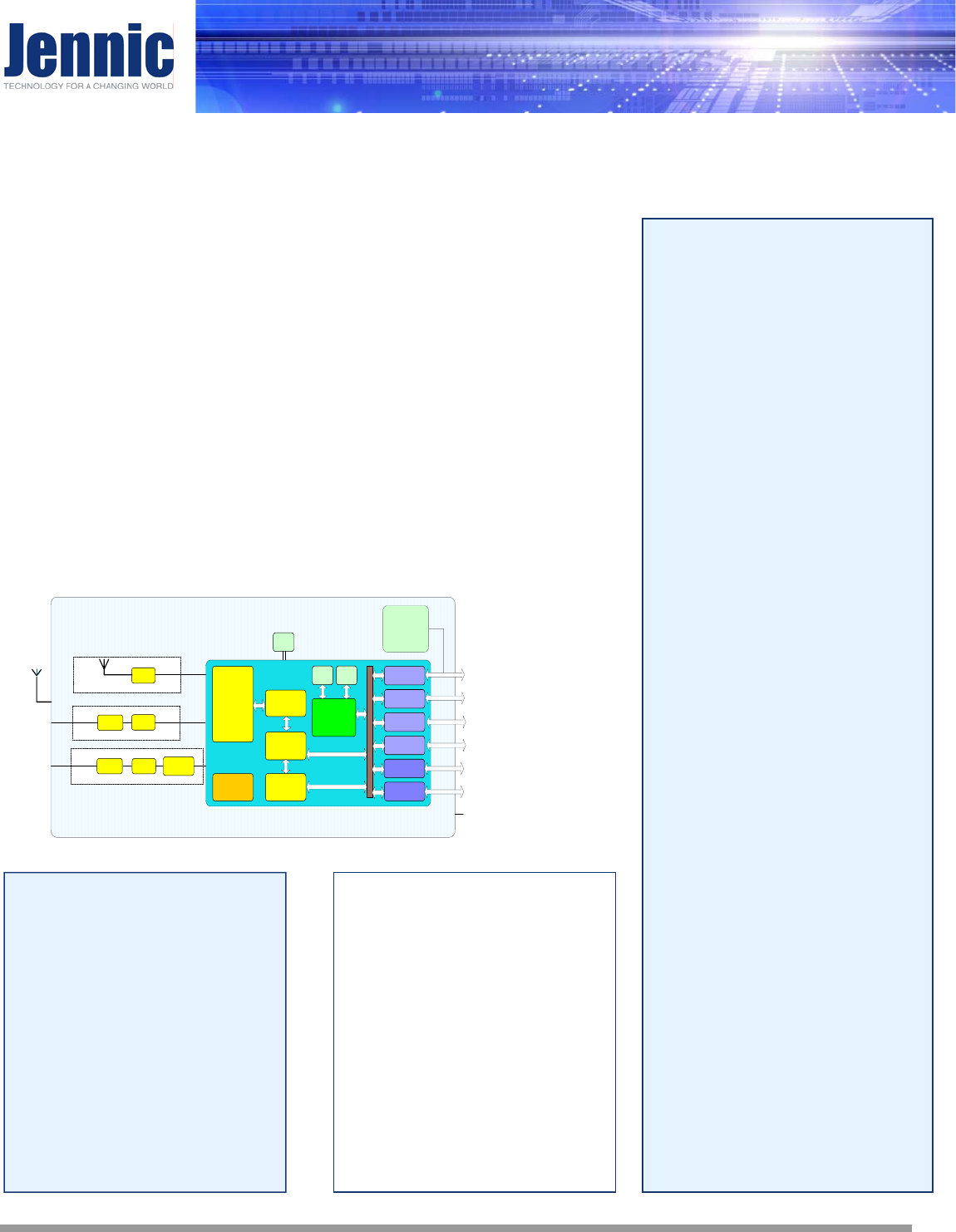
Module Block Diagram
Benefits
x Microminiature module solutions
x Ready to use in products
x Minimises product development
time
x No RF test required for systems
x Compliant with FCC part 15
rules, IC Canada, ETSI ETS
300-328 and Japan ARIB STD-
T66
x Production volumes supplied
pre-programmed with
application software
Applications
x Robust and secure low power
wireless applications
x Wireless sensor networks,
particularly IEEE802.15.4 /
ZigBee systems
x Home and commercial building
automation
x Home networks
x Toys and gaming peripherals
x Industrial systems
x Telemetry and utilities
(e.g. AMR)
Timers
UARTs
12-bit ADC,
comparators
11- bi t DACs,
temp sensor
2-wire seri al
SPI
RAM
96kB
128-bit AES
Encryption
Ac ce l er a to r
2.4GHz
Radi o
ROM
192kB
RI SC CPU
Power
Management
XTAL
O-QPSK
Modem
IEEE802.15.4
MAC
Acc el e r at or
128kB Serial
Flash Memory
JN5139 chip
Power
Bal un
Connector
Bal un
Ceramic Antenna
Bal unConnector PA / LNA
External
Antenna
M00 Opt ion
M01/03 Option
M02/04 Option

Jennic
ii JN-DS-JN5139-xxx-Myy 1v5 © Jennic 2009
Contents
1. Introduction 3
1.1. Variants 3
1.2. Regulatory Approvals 3
2. Specifications 4
3. Product Development 6
3.1. JN5139 Single Chip Wireless Microcontroller 6
4. Pin Configurations 7
4.1. Pin Assignment 8
4.2. Pin Descriptions 9
4.2.1 Power Supplies 9
4.2.2 SPI Memory Connections 9
5. Electrical Characteristics 10
5.1. Maximum Ratings 10
5.2. Reflow Profile 10
5.3. Operating Conditions 11
Appendix A Additional Information 12
A.1 Outline Drawing 12
A.2 Module PCB Footprint 17
A.3 Ordering Information 18
A.4 Tape and Reel Information: 19
A.4.1 Tape Orientation and dimensions 19
A.4.2 Cover tape details 19
A.4.3 Leader and Trailer 20
A.4.4 Reel Dimensions: 20
A.5 Related Documents 21
A.6 Federal Communication Commission Interference Statement 21
A.6.1 Antennas approved by FCC for use with JN5139 modules 22
A.6.2 High Power Module usage limitation 23
A.6.3 FCC End Product Labelling 23
A.7 European R & TTE Directive 1999/5/EC Statement 24
A.8 Industry Canada Statement 25
A.8.1 Industry Canada End Product Labelling 25
A.9 RoHS Compliance 25
A.10 Status Information 26
A.11 Disclaimers 26
A.12 Version Control 27

Jennic
© Jennic 2009 JN-DS-JN5139-xxx-Myy 1v5 3
1. Introduction
The JN5139-xxx-Myy module family provides designers with a ready made component which allows IEEE802.15.4 [1]
wireless applications, using Jennic’s JenNet networking protocol or ZigBee, to be quickly and easily included in
product designs. The modules integrate all of the RF components required, removing the need to perform expensive
RF design and test. Products can be designed by simply connecting sensors and switches to the module IO pins.
The modules use Jennic’s single chip IEEE802.15.4 Wireless Microcontroller, allowing designers to make use of the
extensive chip development support material. Hence, this range of modules allows designers to bring wireless
applications to market in the minimum time with significantly reduced development effort and cost.
Three module hardware variants are available: JN5139-xxx-M00 (standard module with on board ceramic antenna),
JN5139-xxx-M01 (standard module with SMA connector for use with external antennae – recommended for
evaluation use) and JN5139-xxx-M02 (high RF power, improved sensitivity module for evaluation of extended range
applications). For volume production applications, uFL connector variants are provided (-M03 standard power and –
M04 high power). These devices, together with the –M00 variants have FCC modular approvals. Each of these
modules can be supplied with a range of protocol stacks, including JenNet for most tree and linear networks,
IEEE802.15.4 protocol for point-to-point and star applications and a ZigBee mesh networking stack. The variants
available are described below.
1.1. Variants
1.2. Regulatory Approvals
All module types have been tested against the requirements of European standard ETS 300 328 v1.7.1 and a
Notified Body statement of opinion for this standard is available on request. The High Power modules with M02 or
M04 suffix are approved for use in Europe with reduced output power: +10dBm EIRP is the maximum permitted in
Europe. They must not be used with PHY_PIB_ATTR_TX_POWER set above 50 See [3] JN-RM-2002 802.15.4
Stack API.
Additionally, modules with M00, M03 and M04 suffixes have received FCC “Modular Approvals”, in compliance with
CFR 47 FCC part 15 regulations and in accordance to FCC Public notice DA00-1407. The modules are approved for
use with a number of antennase, refer to section A.6.1 for details. See Appendix A.6 for details on the conditions
applying to this modular approval. The modular approvals notice and test reports are available on request.
The high power module variant is classified as ‘mobile’ device pursuant with FCC § 2.1091 and must not be used at a
distance of less than 20 cm (8”) from any person.
In addition, all modules have Industry Canada RSS 210 Issue 7 (June 2007) certification.
Variant Description FCCID Industry Canada ID
JN5139-001-M00 IEEE802.15.4 stack, ceramic antenna TYOJN5139M0 IC: 7438A-CYO5139M0
JN5139-Z01-M00 ZigBee stack, ceramic antenna TYOJN5139M0 IC: 7438A-CYO5139M0
JN5139-001-M01 IEEE802.15.4 stack, SMA connector - for
evaluation N/A IC: 7438A-CYO5139M6
JN5139-Z01-M01 ZigBee stack, SMA connector – for
evaluation N/A IC: 7438A-CYO5139M6
JN5139-001-M02 High Power, IEEE802.15.4 stack, SMA
connector – for evaluation N/A IC: 7438A-CYO5139M4
JN5139-Z01-M02 High Power, ZigBee stack, SMA connector
– for evaluation N/A IC: 7438A-CYO5139M4
JN5139-001-M03 IEEE802.15.4 stack, uFl connector TYOJN5139M3 IC: 7438A-CYO5139M6
JN5139-Z01-M03 ZigBee stack, uFl connector TYOJN5139M3 IC: 7438A-CYO5139M6
JN5139-001-M04 High Power, IEEE802.15.4 stack, uFl
connector TYOJN5139M4 IC: 7438A-CYO5139M4
JN5139-Z01-M04 High Power, ZigBee stack, uFl connector TYOJN5139M4 IC: 7438A-CYO5139M4

Jennic
4 JN-DS-JN5139-xxx-Myy 1v5 © Jennic 2009
2. Specifications
Most specification parameters for the modules are specified in the chip datasheet - JN-DS- JN513x Wireless
Microcontroller Datasheet, [2]. Where there are differences, the parameters are defined here.
VDD=3.0V @ +25°C
Typical DC Characteristics Notes
JN5139-xxx-
M00/01/03
JN5139-xxx-
M02/04
Deep sleep current 1.3uA 1.3uA
Sleep current 2.6uA 2.6uA With active sleep timer
Radio transmit current 37mA 125mA CPU in doze, radio transmitting
Radio receive current 37mA 45mA CPU in doze, radio receiving
Centre frequency accuracy +/-25ppm +/-25ppm Additional +/-15ppm allowance for
temperature and ageing
Typical RF Characteristics Notes
Receive sensitivity -96dBm -102dBm Nominal for 1% PER, as per
802.15.4 section 6.5.3.3 (Note 1)
Maximum Transmit power +1dBm 17.5dBm Nominal (Note 1)
Maximum Transmit power [Boost Mode] +2.5dBm N/A (Note 1)
Transmit power at 3.6V 19dBm With Vdd=3.6V
Maximum input signal +10dBm +10dBm For 1% PER, measured as
sensitivity
RSSI range -95 to -10
dBm
-105 to -20
dBm
RF Port impedance – SMA/uFl connector 50 ohm 50 ohm 2.4 - 2.5GHz
VSWR (max) 2:1 2:1 2.4 - 2.5GHz
Peripherals Notes
Master SPI port 5 selects 3 selects 250kHz - 16MHz
Slave SPI port 99
250kHz - 8MHz
Two UARTs 99
16550 compatible
Two-wire serial I/F (compatible with SMbus & I2C) 99
Up to 400kHz
Two programmable Timer/Counters with
capture/compare facility, Tick timer
99
16MHz clock
Two programmable Sleep Timers 99
32kHz clock
Digital IO lines (multiplexed with UARTs, timers
and SPI selects)
21 19
Four channel Analogue-to-Digital converter 99
12-bit, up to 100ks/s
Two channel Digital-to-Analogue converter 99
11-bit, up to 100ks/s
Two programmable analogue comparators 99
Ultra low power mode for sleep
Internal temperature sensor and battery monitor 99

Jennic
© Jennic 2009 JN-DS-JN5139-xxx-Myy 1v5 5
The performance of all peripherals is defined in the JN-DS- JN513x Wireless Microcontroller Datasheet [2]
Note 1: Sensitivity is defined for conducted measurements on connectorised modules. Modules with an integrated
antenna have approximately 4 dB less e.i.r.p and reciprocal receive sensitivity.

Jennic
6 JN-DS-JN5139-xxx-Myy 1v5 © Jennic 2009
3. Product Development
Jennic supplies all the development tools and networking stacks needed to enable end product development to occur
quickly and efficiently. These are all freely available from Jennic’s support website: http://www.jennic.com/support/ .
A range of evaluation/developer kits is also available, allowing products to be quickly breadboarded. Efficient
development of software applications is enabled by the provision of a complete, unlimited, software developer kit.
Together with the available libraries for the JenNet networking stack, the IEEE802.15.4 MAC and the ZigBee network
stack, this package provides everything required to develop application code and to trial it with hardware
representative of the final module.
The modules can be user programmed both in development and in production using software supplied by Jennic.
They can also be supplied ready loaded with customer defined software if required. Access to the on-chip
peripherals, MAC and network stack software is provided through specific APIs. This information is available on the
Jennic support website, together with many example applications, user guides, reference manuals and application
notes.
3.1. JN5139 Single Chip Wireless Microcontroller
The JN5139-xxx-Myy series is constructed around the JN5139 single chip wireless microcontroller, which includes
the radio system, a 32-bit RISC CPU, ROM and RAM memory and a range of analogue and digital peripherals.
The chip is described fully in JN-DS- JN513x Wireless Microcontroller Datasheet [2].
The module also includes a 1Mbit serial flash memory which holds the application code that is loaded into the
JN5139 during the boot sequence.
Jennic
© Jennic 2009 JN-DS-JN5139-xxx-Myy 1v5 7
4. Pin Configurations
1
2
3
4
16
ADC4
DAC1
DAC2
COMP2+
COMP2-
SPICLK
SPIMISO
SPIMOSI
SPISSZ
DIO0/SPISEL1
DIO1/SPISEL2
DIO2/SPISEL3
SPISSM
SPISWP
DIO3/SPISEL4
DIO4/CTS0
DIO5/RTS0
DIO6/TXD0
DIO7/RXD0
DIO8/TIM0GT
DIO9/TIM0_CAP
DIO10/TIM0_OUT
DIO11/TIM1GT
VDD
GND
VSSA
ADC3
ADC2
ADC1
DIO20/RXD1
DIO19/TXD1
DIO18/RTS1
DIO17/CTS1
DIO16
DIO15/SIF_D
RESETN
DIO14/SIF_CLK
DIO13/TIM1_OUT
DIO12/TIM1_CAP
5
6
7
8
9
10
11
12
13
14
15
17 18 19 20 21 22 23 24 25 26
41
40
39
38
37
36
35
34
33
32
31
30
29
28
27
Antenna
J1
COMP1+
COMP1-
Figure 1: Pin Configuration (top view)
Note that the same basic pin configuration applies for all module designs. However, DIO3/SPISEL4 and
DIO2/SPISEL3 are not available on the high power modules.

Jennic
8 JN-DS-JN5139-xxx-Myy 1v5 © Jennic 2009
4.1. Pin Assignment
Pin Signal Function Alternative Function
1 ADC4 Analogue to Digital input
2 DAC1 Digital to Analogue output
3 DAC2 Digital to Analogue output
4 COMP2+
5 COMP2-
Comparator 2 inputs
6 SPICLK SPI master clock out
7 SPIMISO SPI Master In/Slave Out
8 SPIMOSI SPI Master Out/Slave In
9 SPISSZ SPI select from module - SS0 (output)
10 SPISEL1 SPI Slave Select1 (output) General Purpose Digital I/O DIO0
11 SPISEL2 SPI Slave Select2 (output) General Purpose Digital I/O DIO1
12 SPISEL3* SPI Slave Select3 (output) General Purpose Digital I/O DIO2 *
13 SPISSM SPI select to FLASH (input)
14 SPISWP FLASH write protect (input)
15 SPISEL4* SPI Slave Select4 (output) General Purpose Digital I/O DIO3*
16 CTS0 UART0 Clear To Send (input) General Purpose Digital I/O DIO4
17 RTS0 UART0 Request To Send (output) General Purpose Digital I/O DIO5
18 TXD0 UART0 Transmit Data (output) General Purpose Digital I/O DIO6
19 RXD0 UART0 Receive Data (input) General Purpose Digital I/O DIO7
20 TIM0GT Timer0 clock/gate (input) General Purpose Digital I/O DIO8
21 TIM0_CAP Timer0 capture (input) General Purpose Digital I/O DIO9
22 TIM0_OUT Timer0 PWM (output) General Purpose Digital I/O DIO10
23 TIM1GT Timer1 clock/gate (input) General Purpose Digital I/O DIO11
24 VDD 3V power
25 GND Digital ground
26 VSSA Analogue ground
27 TIM1_CAP Timer1 capture (input) General Purpose Digital I/O DIO12
28 TIM1_OUT Timer1 PWM (output) General Purpose Digital I/O DIO13
29 RESETN Active low reset
30 SIF_CLK Serial Interface clock / Intelligent peripheral clock General Purpose Digital I/O DIO14

Jennic
© Jennic 2009 JN-DS-JN5139-xxx-Myy 1v5 9
Pin Signal Function Alternative Function
31 SIF_D Serial Interface data / Intelligent peripheral data
out (output)
General Purpose Digital I/O DIO15
32 DIO 16 Intelligent peripheral device data in (input) General Purpose Digital I/O
33 CTS1 UART1 Clear To Send (input) / Intelligent
peripheral device select (input)
General Purpose Digital I/O DIO17
34a RTS1 UART1 Request To Send (output) / Intelligent
peripheral interrupt (output)
General Purpose Digital I/O DIO18
35 TXD1 UART1 Transmit Data (output) General Purpose Digital I/O DIO19
36 RXD1 UART1 Receive Data (input) General Purpose Digital I/O DIO20
37 COMP1-
38 COMP1+
Comparator 1 inputs
39 ADC1 Analogue to Digital input
40 ADC2 Analogue to Digital input
41 ADC3 Analogue to Digital input
*: These two pins are not connected for High power modules
4.2. Pin Descriptions
All pins behave as described in the JN-DS- JN513x Wireless Microcontroller Datasheet [2], with the exception of the
following:
4.2.1 Power Supplies
A single power supply pin, VDD is provided. Separate analogue (VSSA) and digital (GND) grounds are provided.
These should be connected together at the module pins.
4.2.2 SPI Memory Connections
SPISWP is a write protect pin for the serial flash memory. This should be held low to inhibit writes to the flash device.
SPISSZ is connected to SPI Slave Select 0 on the JN5139.
SPISSM is connected to the Slave Select pin on the memory.
This configuration allows the flash memory device to be programmed using an external SPI programmer if required.
For programming in this mode, the JN5139 should be held in reset by taking RESETN low.
The memory can also be programmed over the UART by using the flash programmer software provided by Jennic.
This is available as part of the Software Developer kit and libraries available from Jennic’s support website –
www.jennic.com/support. To enter this programming mode, SPIMISO (pin 7) should be held low whilst the chip is
reset. Once programming has finished, the chip should be reset, when it will execute the new code downloaded.
For normal operation of the module and programming over the UART, SPISSZ should be connected to
SPISSM.
Jennic
10 JN-DS-JN5139-xxx-Myy 1v5 © Jennic 2009
5. Electrical Characteristics
In most cases, the Electrical Characteristics are the same for both module and chip. They are described in detail in
the chip datasheet. Where there are differences, they are detailed below.
5.1. Maximum Ratings
Exceeding these conditions will result in damage to the device.
Parameter Min Max
Device supply voltage VDD -0.3V 3.6V
Voltage on analogue pins: ADC1-4, DAC1-2, COMP1-,
COMP1+, COMP2-, COMP2+, DIO9, DIO10, SPISSM,
SPISWP, SPICLK, SPIMOSI, SPIMISO,
-0.3V VDD + 0.3V
Voltage on 5v tolerant digital pins: SPISSZ, DIO0-
DIO8, DIO11-DIO20, RESETN
-0.3V Lower of (VDD + 2V)
and 5.5V
Storage temperature -40ºC 150ºC
Reflow soldering temperature according to IPC/JEDEC
J-STD-020C
260ºC
This device is sensitive to ESD and should only be handled using ESD precautions.
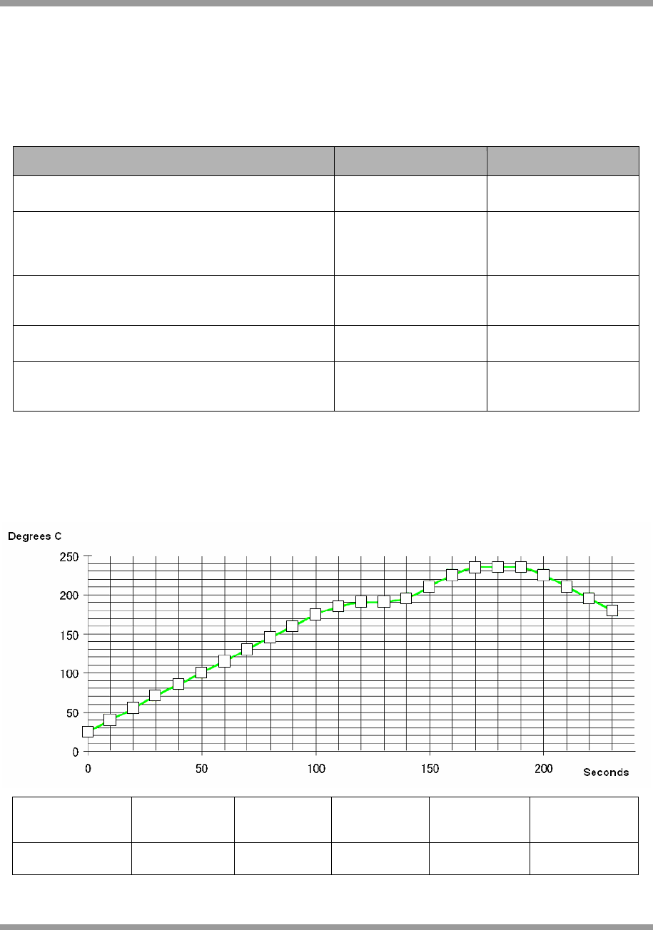
5.2. Reflow Profile
For reflow soldering, it is recommended to follow the reflow profile in Figure 2 as a guide, as well as the paste
manufacturers guidelines on peak flow temperature, soak times, time above liquidus and ramp rates.
Figure 2: Recommended solder reflow profile
Temperature 25~160 ºC 160~190 ºC > 220º C 230~Pk. Pk. Temp
(235ºC)
Target Time (s) 90~130 30~60 20~50 10~15 160~270

Jennic
© Jennic 2009 JN-DS-JN5139-xxx-Myy 1v5 11
5.3. Operating Conditions
Supply Min Max
VDD 2.7V 3.6V
Ambient temperature range -20°C 70°C
Jennic
12 JN-DS-JN5139-xxx-Myy 1v5 © Jennic 2009
Appendix A Additional Information
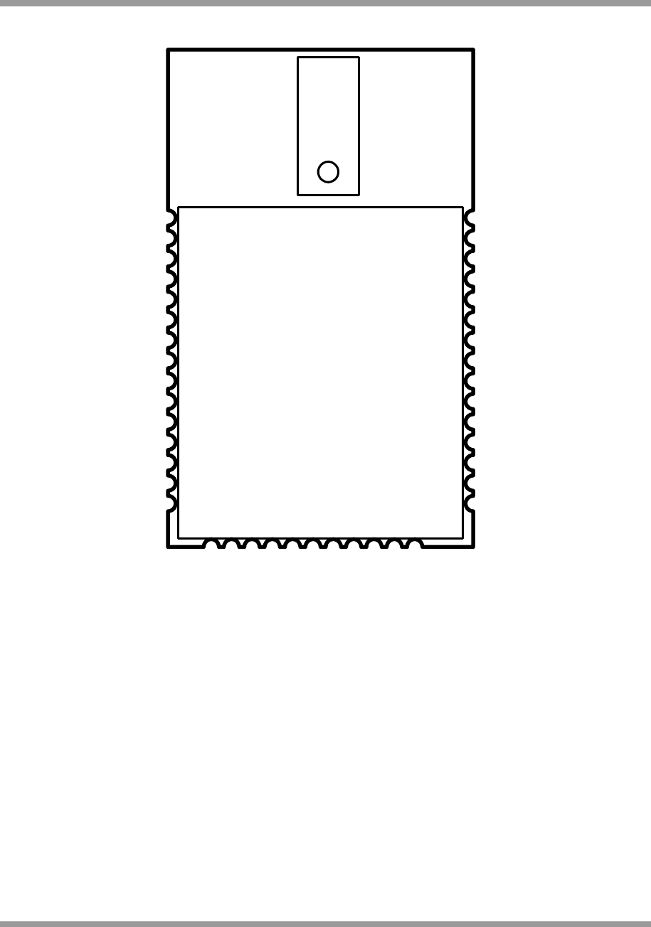
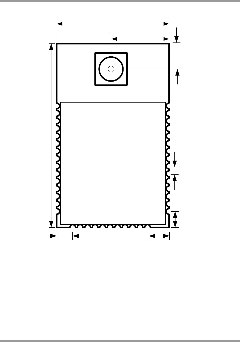
A.1 Outline Drawing
Antenna
30mm
18mm
J1
2.76
mm
2.54
mm
2.54
mm
1.27
mm
Thickness: 3.5mm
Figure 3 JN5139-xxx-M00 Outline Drawing
Jennic
© Jennic 2009 JN-DS-JN5139-xxx-Myy 1v5 13
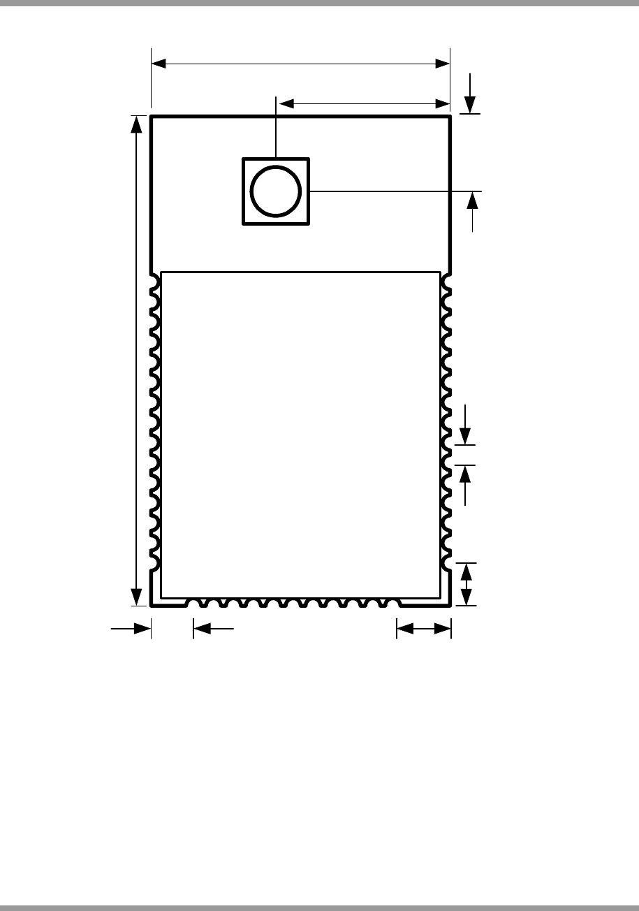
30mm
18mm
2.76
mm
2.54
mm
2.54
mm
4.59
mm
9.74mm
1.27
mm
Thickness: 3.5mm over can, 10.8mm at SMA connector
Figure 4 JN5139-xxx-M01 Outline Drawing
Jennic
14 JN-DS-JN5139-xxx-Myy 1v5 © Jennic 2009
30mm
18mm
2.76
mm
2.54
mm
2.54
mm
6.58
mm
9.76mm
1.27
mm
Thickness: 3.5mm
Figure 5 JN5139-xxx-M03 Outline Drawing
Jennic
© Jennic 2009 JN-DS-JN5139-xxx-Myy 1v5 15
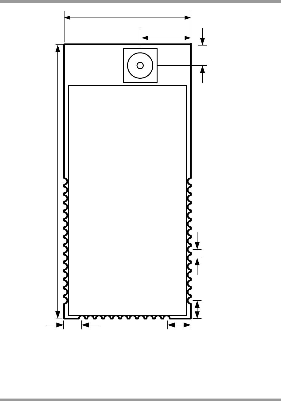
41mm
18mm
.
2.76
mm
2.54
mm
1.27
mm
2.54
mm
4.32
mm
7.2mm
Thickness: 3.5mm over can, 10.8mm at SMA connector.
Figure 6 JN5139-xxx-M02 Outline Drawing
Jennic
16 JN-DS-JN5139-xxx-Myy 1v5 © Jennic 2009
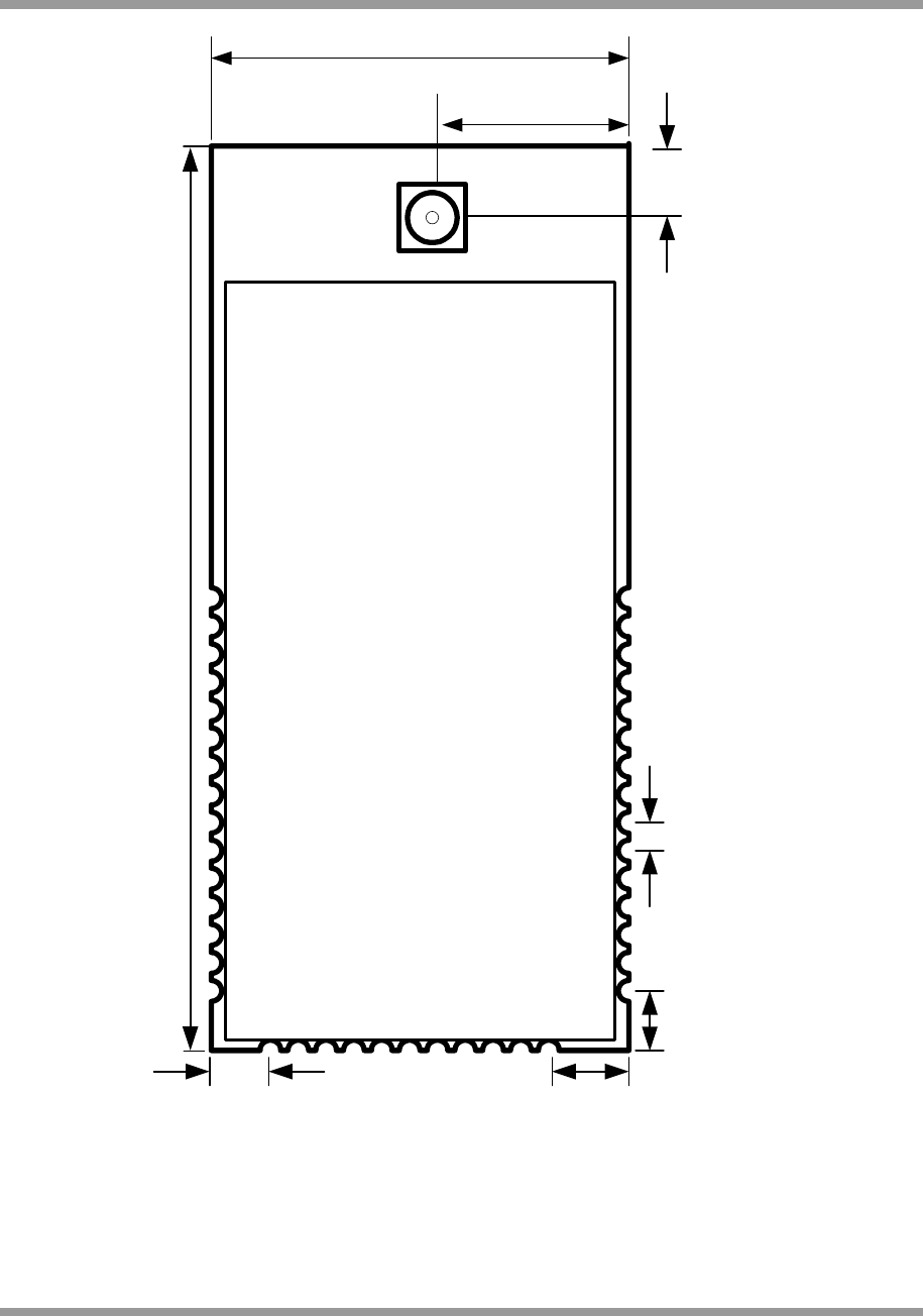
40.5mm
18mm
.
2.76
mm
2.54
mm
1.27
mm
2.54
mm
4.05mm
7.2mm
Thickness: 3.5mm
Figure 7 JN5139-xxx-M04 Outline Drawing
Jennic
© Jennic 2009 JN-DS-JN5139-xxx-Myy 1v5 17
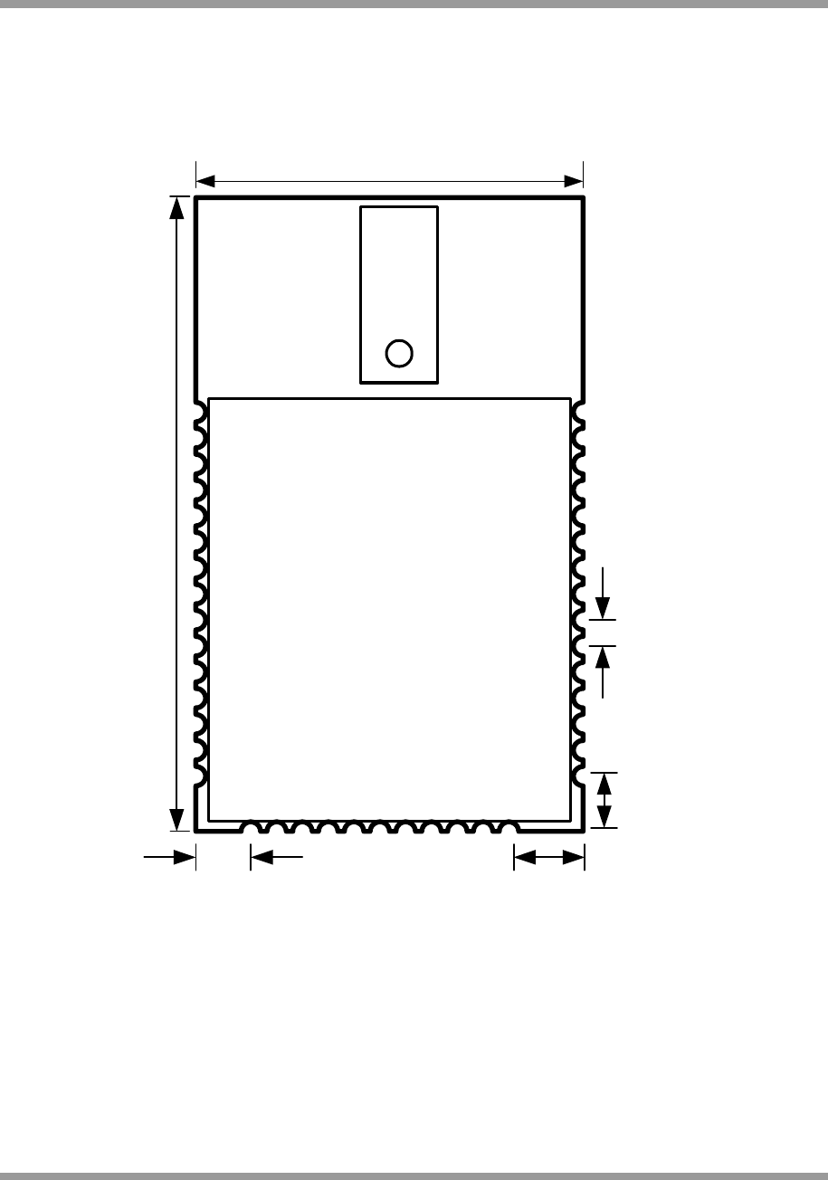
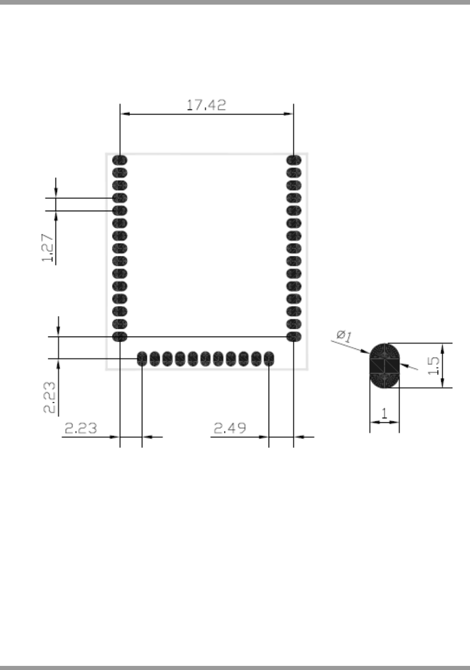
A.2 Module PCB Footprint
Dimensions in mm
Note: All modules have the same footprint.
Figure 8 Module PCB footprint
RF note for –M00 modules with ceramic antenna: No components, ground plane or tracks on any layer of
the mother board should be placed within 20mm of the 3 free sides of the antenna. Tracks etc may be placed
adjacent to the can, but should not extend past the can towards the antenna end of the module for 20mm
from the antenna.
Jennic
18 JN-DS-JN5139-xxx-Myy 1v5 © Jennic 2009
A.3 Ordering Information
Software Variant
001 IEEE802.15.4 Stack
Z01 ZigBee Stack
Shipping
X Tape mounted samples up to 50 pieces
T Tape Mounted 500pieces reel (00, 03, 04 modules only)
V Tape Mounted 200pieces reel (01,02 modules only)
JN5139 - XXX - MY1Y2 Y3 Y4
Temp Range / Device Status
blank -20qC to +70qC, qualified
Module Type
00 Standard Power, Ceramic antenna
01 Standard Power, SMA connector
02 High Power, SMA connector
03 Standard Power, uFl connector – use for new designs
04 High power, uFl connector– use for new designs
Label line 1: IC ID Number
Label line 2: FCC ID Number
Label line 3: Part Name
Label line 4: Barcode Label
Label line 5: YYWWTNNNNN (see below)
Identifier Description Format
YY Year 06(example)
WW Week 45(example)
T Module type
NNNNN Serial
Number
YYWWTNNNNN
IC: 7438A-CYO5139M0
FCC ID: TYOJN5139M0
JN51XX-XXX-XXX JENNIC
Figure 9: Example module labelling for FCC approved modules
Jennic
© Jennic 2009 JN-DS-JN5139-xxx-Myy 1v5 19
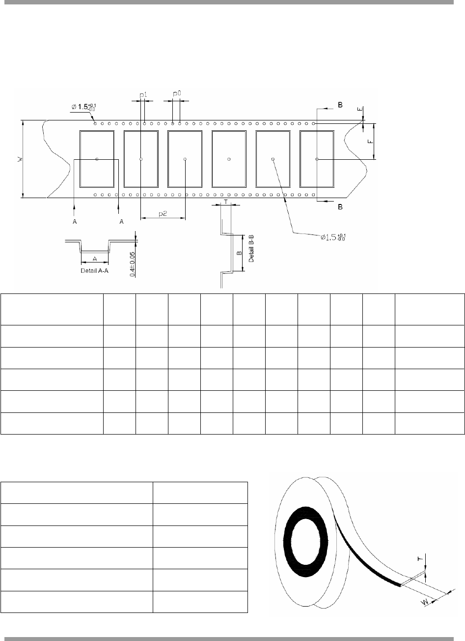
A.4 Tape and Reel Information:
A.4.1 Tape Orientation and dimensions
All dimensions are in mm
Module type: A B W F E P0 P1 P2 T Cover Tape
width (W)
JN5139-xxx-M00/03 18.4 30.4 44 20.2 1.75 4.0 2.0 24.0 3.4 37.5
JN5139-xxx-M01 18.4 30.4 56 26.2 1.75 4.0 2.0 24.0 11.2 49.5
JN5139-xxx-M02 18.5 41.5 56 26.2 1.75 4.0 2.0 24.0 11.1 49.5
JN5139-xxx-M04 18.5 40.9 56 26.2 1.75 4.0 2.0 24.0 3.4 49.5
Tolerance ±0.1 ±0.1 ±0.3 ±0.1 +0.1 ±0.1 ±0.1 ±0.1 ±0.1 ±0.1
A.4.2 Cover tape details
Thickness (T) 0.061mm
Surface resistivity (component side) 104 to 107 Ohms/sq
Surface resistivity (component side) Non-conductive
Backing type: Polyester
Adhesive type: PSA
Sealing: Room ambient
Jennic
20 JN-DS-JN5139-xxx-Myy 1v5 © Jennic 2009
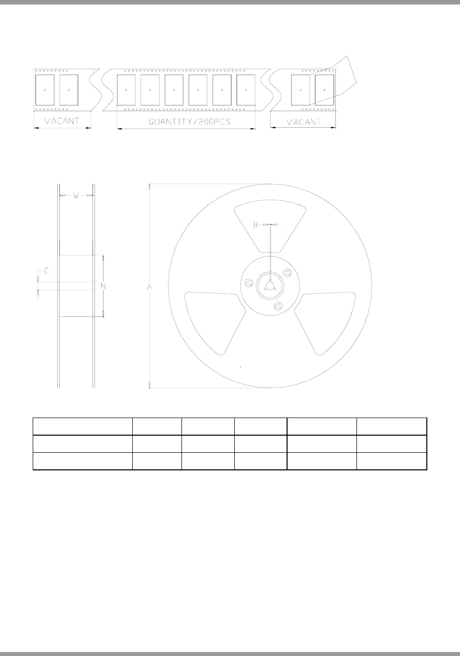
A.4.3 Leader and Trailer
300 MM300 MM
A.4.4 Reel Dimensions:
Dimensions in mm
Module type: A B C N W (min)
JN5139-xxx-M00/03 330 ±1.0 2.2±0.5 13 ±0.2 100 +0.1 44.5 ±0.3
JN5139-xxx-M01/02/04 330 ±1.0 2.2±0.5 13 ±0.2 100 +0.1 56.5 ±0.3

Jennic
© Jennic 2009 JN-DS-JN5139-xxx-Myy 1v5 21
A.5 Related Documents
[1] IEEE Std 802.15.4-2003 IEEE Standard for Information Technology – Part 15.4 Wireless Medium Access Control
(MAC) and Physical Layer (PHY) Specifications for Low-Rate Wireless Personal Area Networks (LR-WPANs)
[2] JN-DS- JN513x Wireless Microcontroller Datasheet
[3] JN-RM-2002 802.15.4 Stack API
A.6 Federal Communication Commission Interference Statement
This equipment has been tested and found to comply with the limits for a Class B digital device, pursuant to Part 15
of the FCC Rules. These limits are designed to provide reasonable protection against harmful interference in a
residential installation. This equipment generates, uses, and can radiate radio frequency energy and, if not installed
and used in accordance with the instructions, may cause harmful interference to radio communications. However,
there is no guarantee that interference will not occur in a particular installation. If this equipment does cause harmful
interference to radio or television reception, which can be determined by turning the equipment off and on, the user is
encouraged to try to correct the interference by one of the following measures:
- Reorient or relocate the receiving antenna.
- Increase the separation between the equipment and receiver.
- Connect the equipment into an outlet on a circuit different from that to which the receiver is connected.
- Consult the dealer or an experienced radio/TV technician for help.
This device complies with Part 15 of the FCC Rules. Operation is subject to the following two conditions: (1) This
device may not cause harmful interference, and (2) this device must accept any interference received, including
interference that may cause undesired operation.
FCC Caution: Any changes or modifications not expressly approved by the party responsible for compliance could
void the user's authority to operate this equipment.
WARNING!
FCC Radiation Exposure Statement:
This portable equipment with its antenna complies with FCC’s RF radiation exposure limits set forth for an
uncontrolled environment. To maintain compliance follow the instructions below;
1. This transmitter must not be co-located or operating in conjunction with any other antenna or transmitter.
2. Avoid direct contact to the antenna, or keep it to a minimum while using this equipment.
This transmitter module is authorized to be used in other devices only by OEM integrators under the
following condition:
The transmitter module must not be co-located with any other antenna or transmitter.
As long as the above condition is met, further transmitter testing will not be required. However, the OEM integrator is
still responsible for testing their end product for any additional compliance requirements required with this module
installed (for example, digital device emissions, PC peripheral requirements, etc.).

Jennic
22 JN-DS-JN5139-xxx-Myy 1v5 © Jennic 2009
A.6.1 Antennas approved by FCC for use with JN5139 modules
Brand Model Number Description Gain (dBi) Connector type
1 Aveslink Technology, Inc E-0360-AT Patch Antenna - outdoor 18 RP-N 1
2 Aveslink Technology, Inc E-0260-AT Patch Antenna - outdoor 15 RP-N 1
3 Aveslink Technology, Inc E-1050-AT Vertical - outdoor colinear 15 RP-N
4 Aveslink Technology, Inc E-1040-AT Vertical - outdoor colinear 12 RP-N
5 Aveslink Technology, Inc E-0100-AC Patch Antenna - flying lead 10 RP-SMA
6 Aveslink Technology, Inc E-1030-AT Vertical - outdoor colinear 9 RP-N
7 Aveslink Technology, Inc E-1020-AT Vertical - outdoor colinear 7 RP-N
8 Aveslink Technology, Inc E-1710-GC Vertical - swivel 7 RP-SMA
9 Aveslink Technology, Inc E-1710-GM Vertical - swivel 7 RP-TNC
10 Aveslink Technology, Inc E-1511-GC Vertical - swivel 5 RP-SMA
11 Aveslink Technology, Inc E-0030-AA Patch Antenna - flying lead 4 uFL
12 Aveslink Technology, Inc E-0030-AC Patch Antenna - flying lead 4 RP-SMA
13 Aveslink Technology, Inc E-1204-AC Ceiling antenna - flying lead 4 RP-SMA
14 Aveslink Technology, Inc E-1520-CA Vertical - bulkhead- flying lead 4 uFL
15 Aveslink Technology, Inc E-1520-GC Vertical - swivel 4 RP-SMA
16 Aveslink Technology, Inc E-1450-GC Vertical-swivel mount 4 RP-SMA
17 Nearson S152CL-L-PX-2450S Vertical - knuckle-flying lead 4 uFL
18 Antenna Factor ANT-2.4-CW-RCL Vertical - knuckle antenna 2.9 RP-SMA
19 Aveslink Technology, Inc E-0901-AA Embedded - flying lead 2.5 uFL
20 Antenna Factor ANT-2.4-CW-RCT-RP Vertical - knuckle antenna 2.2 RP-SMA
21 Antennova 2010B6090-01 Vertical - knuckle antenna 2.2 RP-SMA
22 Hyperlink Technology HG2402RD-RSF Vertical - knuckle antenna 2.2 RP-SMA
23 Aveslink Technology, Inc E-0005-AC Vertical- flying lead 2 RP-SMA
24 Aveslink Technology, Inc E-2411-GC Vertical - swivel 2 RP-SMA
25 Aveslink Technology, Inc E-2410-CA Vertical - bulkhead- flying lead 2 uFL
26 Aveslink Technology, Inc E-2410-GC Vertical - swivel 2 RP-SMA
27 Aveslink Technology, Inc E-2820-CA Vertical - bulkhead- flying lead 2 uFL
28 Aveslink Technology, Inc E-2820-GC Vertical - swivel 2 RP-SMA
29 Aveslink Technology, Inc E-0903-AX Embedded - nickel silver strip 2 None
30 Aveslink Technology, Inc E-0904-AX Embedded - nickel silver strip 2 None
31 Embedded Antenna Design FBKR35068-RS-KR Vertical - knuckle antenna 2 RP-SMA
32 Nearson S131CL-L-PX-2450S Vertical - knuckle-flying lead 2 uFL
33 Laird Technologies WRR2400-IP04 Vertical - knuckle-flying lead 1.5 uFL
34 Laird Technologies WRR2400-RPSMA Vertical - knuckle-flying lead 1.3 RP-SMA
35 Aveslink Technology, Inc E-6170-DA Vertical - right angle 1 uFL
36 Laird Technologies WCR2400-SMRP Vertical - knuckle antenna 1 RP-SMA
These antennae or versions with alternative connectors may be used to meet European regulations, provided the
gain is less than 4.4dBi.
1 These antennas may not be used with High Power Modules

Jennic
© Jennic 2009 JN-DS-JN5139-xxx-Myy 1v5 23
This device has been designed to operate with the antennas listed above. Antennas not included in this list or having
a gain greater than 18 dBi are strictly prohibited for use with this device. The required antenna impedance is 50ohms.
A.6.2 High Power Module usage limitation
The high power module variants are classified as ‘mobile’ device pursuant with FCC § 2.1091 and must not be used
at a distance of < 20 cm (8”) from any nearby people.
IMPORTANT NOTE: In the event that these conditions can not be met (for certain configurations or co-location with
another transmitter), then the FCC authorization is no longer considered valid and the FCC ID can not be used on the
final product. In these circumstances, the OEM integrator will be responsible for re-evaluating the end product
(including the transmitter) and obtaining a separate FCC authorization.
The OEM integrator has to be aware not to provide information to the end user regarding how to install or remove this
RF module in the user manual of the end product.
The user manual for the end product must include the following information in a prominent location;
“To comply with FCC’s RF radiation exposure requirements, the antenna(s) used for this transmitter must not be co-
located or operating in conjunction with any other antenna or transmitter.”
A.6.3 FCC End Product Labelling
The final ‘end product’ should be labelled in a visible area with the following:
“Contains TX FCC ID: TYOJN5139M0, TYOJN5139M3 or TYOJN5139M4 ” to reflect the version of the module being
used inside the product.

Jennic
24 JN-DS-JN5139-xxx-Myy 1v5 © Jennic 2009
A.7 European R & TTE Directive 1999/5/EC Statement
All modules listed in this datasheet are compliant with ETSI EN 300 328V1.7.1 (2006/05) and are subject to Notified
Body Opinion RU1548/9025 Issue 2.
The modules are approved for use with the antennas listed in the following table. The high power modules M02 and
M04 are limited to an antenna with a gain of 2.2 dBi or less.
Brand Model Number Description Gain Connector type
Antenna Factor ANT-2.4-CW-RCL Vertical - knuckle antenna 2.9dBi RP-SMA
Antenna Factor ANT-2.4-CW-RCT-SS Vertical - knuckle antenna 2.2dBi SMA
Laird Technologies WCR2400-SMA Vertical - knuckle antenna 1.0dBi SMA
Laird Technologies WRR2400-IP04 Vertical - knuckle-flying lead 1.5dBi uFL
Embedded Antenna Design BKR2400 Vertical - knuckle antenna 2.0dBi SMA
Antennova Titanis Vertical - knuckle antenna 4.4dBi SMA
Nearson S131CL-L-PX-2450S Vertical - knuckle-flying lead 2.0dBi uFL
Nearson S152CL-L-PX-2450S Vertical - knuckle-flying lead 4.0dBi uFL
Aveslink Technology, Inc E-0030-AA Patch Antenna - flying lead 4dBi uFL
Aveslink Technology, Inc E-0030-AB Patch Antenna - flying lead 4dBi SMA
Aveslink Technology, Inc E-1204-AB Ceiling antenna - flying lead 4dBi SMA
Aveslink Technology, Inc E-0005-AB Vertical- flying lead 2dBi SMA
Aveslink Technology, Inc E-1450-GB Vertical-swivel mount 4dBi SMA
Aveslink Technology, Inc E-1450-GC Vertical-swivel mount 4dBi RP-SMA
Aveslink Technology, Inc E-1520-CA Vertical - bulkhead- flying lead 4dBi uFL
Aveslink Technology, Inc E-1520-GB Vertical - swivel 4dBi SMA
Aveslink Technology, Inc E-1520-GC Vertical - swivel 4dBi RP-SMA
Aveslink Technology, Inc E-2411-GB Vertical - swivel 2dBi SMA
Aveslink Technology, Inc E-2410-CA Vertical - bulkhead- flying lead 2dBi uFL
Aveslink Technology, Inc E-2410-GB Vertical - swivel 2dBi SMA
Aveslink Technology, Inc E-2410-GC Vertical - swivel 2dBi RP-SMA
Aveslink Technology, Inc E-2410-HA Vertical - swivel -flying lead 2dBi uFL
Aveslink Technology, Inc E-2820-CA Vertical - bulkhead- flying lead 2dBi uFL
Aveslink Technology, Inc E-2820-GB Vertical - swivel 2dBi SMA
Aveslink Technology, Inc E-2820-GC Vertical - swivel 2dBi RP-SMA
Aveslink Technology, Inc E-6170-DA Vertical - right angle 1dBi uFL
Aveslink Technology, Inc E-0901-AA Embedded - flying lead 2.5dBi uFL
Hyperlink Technologies HG2402RD-RSF Vertical – tilt and swivel 2.2dBi RP-SMA

Jennic
© Jennic 2009 JN-DS-JN5139-xxx-Myy 1v5 25
A.8 Industry Canada Statement
To reduce potential radio interference to other users, the antenna type and its gain should be so chosen that the
equivalent isotropically radiated power (e.i.r.p.) is not more than that permitted for successful communication.
These modules have been designed to operate with antennas having a maximum gain of 4.4 dBi. Antennas having a
gain greater than 4.4 dBi are strictly prohibited for use with this device. The required antenna impedance is 50 ohms.
The following table shows the approved list of antennas:
Brand Model Number Description Gain
Antenna Factor ANT-2.4-CW-RCL Knuckle Antenna 2.9 dBi
Antenna Factor ANT-2.4-CW-RCT-RP Knuckle Antenna 2.2 dBi
Centurion WCR2400-SMRP Knuckle Antenna 1.0 dBi
Centurion WRR2400-SMRP Knuckle Antenna 1.3 dBi
Nearson S131CL-L-PX-2450S Knuckle Antenna 2.0 dBi
Nearson S141AH-2450 Knuckle Antenna 2.0 dBi
Nearson S152CL-L-PX-2450S Knuckle Antenna 4.0 dBi
Hyperlink Technologies HG2402RD-RSF Knuckle Antenna 2.2 dBi
As long as the above condition is met, further transmitter testing will not be required. However, the OEM integrator is
still responsible for testing their end-product for any additional compliance requirements required with this module
installed (for example, digital device emissions, PC peripheral requirements, etc).
A.8.1 Industry Canada End Product Labelling
For Industry Canada purposes the following should be used.
“Contains Industry Canada ID IC: 7438A-CYO5139M0, IC: 7438A-CYO5139M4 or IC: 7438A-CYO5139M6” to reflect
the version of the module being used inside the product.
A.9 RoHS Compliance
JN5139-xxx-Myy devices meet the requirements of Directive 2002/95/EC of the European Parliament and of the
Council on the Restriction of Hazardous Substance (RoHS).
The JN5139-xxx-M00, M03 and M04 modules are fully compliant with the Chinese RoHS requirements SJ/T11363-
2006.
Further information can be found on the Jennic support website at www.jennic.com/support

Jennic
26 JN-DS-JN5139-xxx-Myy 1v5 © Jennic 2009
A.10 Status Information
The status of this Data Sheet is Production.
Jennic products progress according to the following format:
Advanced
The Data Sheet shows the specification of a product in planning or in development.
The functionality and electrical performance specifications are target values and may be used as a guide to the final
specification.
Jennic reserves the right to make changes to the product specification at anytime without notice.
Preliminary
The Data Sheet shows the specification of a product that is in production, but is not yet fully qualified.
The functionality of the product is final. The electrical performance specifications are target values and may used as a
guide to the final specification. Modules are identified with an R1 suffix, for example JN5139-Z01-M00R1.
Jennic reserves the right to make changes to the product specification at anytime without notice.
Production
This is the final Data Sheet for the product.
All functional and electrical performance specifications, including minimum and maximum values are final.
This Data Sheet supersedes all previous document versions.
Jennic reserves the right to make changes to the product specification at anytime to improve its performance.
A.11 Disclaimers
The contents of this document are subject to change without notice. Jennic reserves the right to make changes,
without notice, in the products, including circuits and/or software, described or contained herein in order to improve
design and/or performance. Information contained in this document regarding device applications and the like is
intended through suggestion only and may be superseded by updates. It is your responsibility to ensure that your
application meets with your specifications.
Jennic warrants performance of its hardware products to the specifications applicable at the time of sale in
accordance with Jennic’s standard warranty. Testing and other quality control techniques are used to the extent
Jennic deems necessary to support this warranty. Except where mandatory by government requirements, testing of
all parameters of each product is not necessarily performed.
Jennic assumes no responsibility or liability for the use of any of these products, conveys no license or title under any
patent, copyright, or mask work right to these products, and makes no representations or warranties that these
products are free from patent, copyright, or mask work infringement, unless otherwise specified.
Jennic products are not intended for use in life support systems, appliances or systems where malfunction of these
products can reasonably be expected to result in personal injury, death or severe property or environmental damage.
Jennic customers using or selling these products for use in such applications do so at their own risk and agree to fully
indemnify Jennic for any damages resulting from such use.
All trademarks are the property of their respective owners.

Jennic
© Jennic 2009 JN-DS-JN5139-xxx-Myy 1v5 27
A.12 Version Control
Version Notes
1.0 1st Issue of Advanced Datasheet
1.1 Update to correct connector positions on drawings and typo on module numbering. –000 modules now
read –001.
1.2 Updated to preliminary status, solder reflow profile and antenna lists added. Increased length of –M02
variants
1.3 Updated part numbering and addition of Industry Canada approvals
1.4 Minor specification updates
1.5 Updated to Production status, updated antenna information and other minor specification updates
Jennic Ltd
Furnival Street
Sheffield
S1 4QT
United Kingdom
Tel: +44 (0)114 281 2655
Fax: +44 (0) 114 281 2951
E-mail: info@jennic.com
For the contact details of your local Jennic office or distributor, refer to the Jennic web site:
www.jennic.com