Nokia Solutions and Networks FZCWM2A1 Wi-Fi AP Module 802.11 ac User Manual M2A AC210m front
Nokia Solutions and Networks, OY Wi-Fi AP Module 802.11 ac M2A AC210m front
Contents
- 1. User Manual (Statements) rev.pdf
- 2. User Manual rev.pdf
- 3. User Manual (System)
User Manual rev.pdf
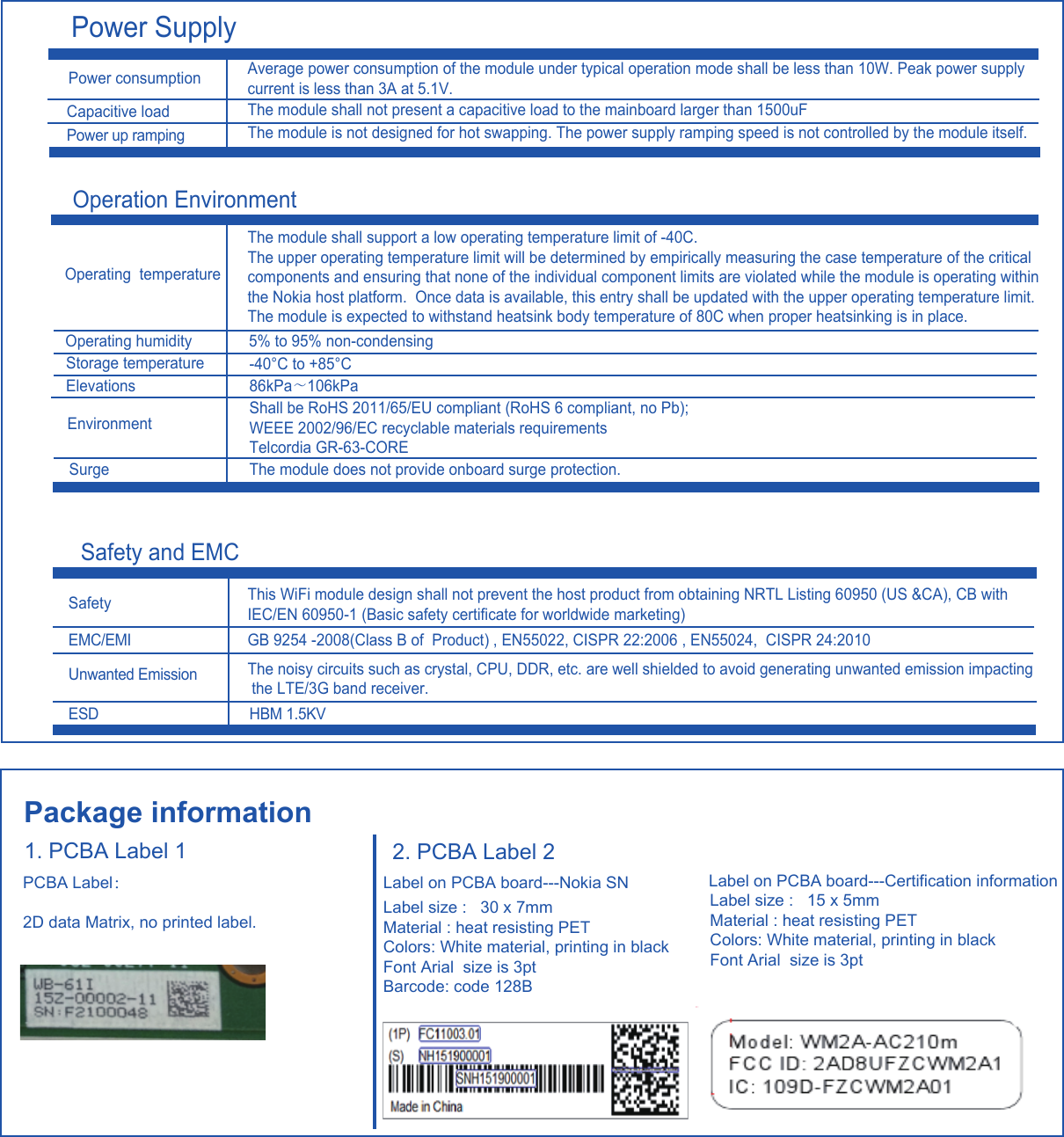
![Interface DefinitionAC210MWi-Fi AP Module DatasheetIntroductionThe AC210M is a high-performance 2x2 802.11a/b/g/n/ac Wi-Fi AP module. It supports simultaneous operation of 2.4 GHz and 5 GHz frequency bands. The module provides two MMCX RF connectors for combined 2.4G and 5G radio and one 60-pin board-to-board connector for connection to the host system. The module communicates with the host system through an 82-pin connector (the Wi-Fi modules populate 60-pin only). The connector on the module is Molex 171810-1115.The connector definition follows Nokia RF and WiFi Card Interface Pinout.xlsx rev 11.Signal DefinitionRFPinWiFiPinStdUseWiFi Card Usage RF Card Usage I/O Voltage ACCouplingPull-up/downMBDir1 - Gnd not present GND2 - DP not present SYNCINB0_MB_RF_DN lvds_1.8v - - O3 - DP not present SYNCINB0_MB_RF_DP lvds_1.8v - - O4 - Gnd not present GND5 - DP not present SERDOUT1_RF_MB_DN cml_1.8v mb, 0.1uF - I6 - DP not present SERDOUT1_RF_MB_DP cml_1.8v mb, 0.1uF - I7 - Gnd not present GND8 - DP not present SERDIN0_MB_RF_DN cml_1.8v rf, 0.1uF - O9 - DP not present SERDIN0_MB_RF_DP cml_1.8v rf, 0.1uF - O10 - Gnd not present GND11 - Extra not present GP_INTERRUPT cmos_[VDD_IF] - mb, 4.7K, gnd I12 1 Gnd GND GND13 2 DP Reserved SYNCOUTB0_RF_MB_DPlvds_1.8v - - I14 3 DP Reserved SYNCOUTB0_RF_MB_DNlvds_1.8v - - I15 4 Gnd GND GND16 5 DP SGMII_1_WIFI_MB_DP SERDOUT2_RF_MB_DPsgmii_1.2v/cml_1.8vmb, 0.1uF - I17 6 DP SGMII_1_WIFI_MB_DN SERDOUT2_RF_MB_DNsgmii_1.2v/cml_1.8vmb, 0.1uF - I18 7 Gnd GND GND19 8 DP SGMII_0_WIFI_MB_DP SERDOUT3_RF_MB_DPsgmii_1.2v/cml_1.8vmb, 0.1uF - I20 9 DP SGMII_0_WIFI_MB_DN SERDOUT3_RF_MB_DNsgmii_1.2v/cml_1.8vmb, 0.1uF - I21 10 Gnd GND GND22 11 DP Reserved RX_MYK_ENABLE cmos_[VDD_IF] - rf, 4.7K, gnd O23 12 DP Reserved RX_LNA_ENABLE_MAINcmos_[VDD_IF] - rf, 4.7K, gnd O24 13 Gnd Reserved RX_LNA_ENABLE_DIV cmos_[VDD_IF] - rf, 4.7K, gnd O25 14 Extra Reserved TX_MYK_ENABLE cmos_[VDD_IF] - rf, 4.7K, gnd O26 15 Extra Reserved TX_KEY_MAIN cmos_[VDD_IF] - rf, 4.7K, gnd O27 16 Extra Reserved TX_KEY_DIV cmos_[VDD_IF] - rf, 4.7K, gnd O28 17 Gnd Reserved TR_SWITCH_MAIN cmos_[VDD_IF] - rf, 4.7K, gnd O29 18 DP Reserved TR_SWITCH_DIV cmos_[VDD_IF] - rf, 4.7K, gnd O30 19 DP I2C_9550_SCL (for test)Reserved n/c on mb - - n/a31 20 GndI2C_9550_SDA (for test)GNDn/c on mb wifi slot- - n/a32 21 DP TRSTn GPIO4 (TRSTn) n/c on mb - - n/a33 22 DP TDO GPIO5 (TDO) n/c on mb - - n/a34 23 Gnd TDI GPIO6 (TDI) n/c on mb - - n/a35 24 DP TMS GPIO7 (TMS) n/c on mb - - n/a36 25 DP TCK GPIO8 (TCK) n/c on mb - - n/a37 26 Gnd Reserved TEST n/c on mb - rf, 1K, gnd n/a38 27 DP 5V_SENSE 5V_SENSE ana_5.1v - - I39 28 DP VCC_5.1V VCC_5.1V40 29 Gnd VCC_5.1V VCC_5.1V41 30 Extra VCC_5.1V VCC_5.1V58 36 DPSGMII_1_MB_WIFI_DPSERDIN2_MB_RF_DPsgmii_1.2v/cml_1.8vrf/wifi, 0.1uF- O59 37 DPSGMII_1_MB_WIFI_DNSERDIN2_MB_RF_DNsgmii_1.2v/cml_1.8vrf/wifi, 0.1uF- O60 38 Gnd GND GND61 39 DP SGMII_0_MB_WIFI_DPSERDIN3_MB_RF_DPsgmii_1.2v/cml_1.8vrf/wifi, 0.1uF- O62 40 DP SGMII_0_MB_WIFI_DNSERDIN3_MB_RF_DNsgmii_1.2v/cml_1.8vrf/wifi, 0.1uF- O63 41 Gnd GND GND64 42 DP I2C_SCL I2C_SCL cmos_3.3v -mb 1K; rf/wifi 10K, 3.3vI/O65 43 DP I2C_SDA I2C_SDA cmos_3.3v -mb 1K; rf/wifi 10K, 3.3vI/O66 44 Gnd GND GND67 45 Extra Reserved SPI_SCLK cmos_[VDD_IF] - rf, 4.7k, gnd O68 46 Extra UART_WIFI_MB SPI_MISO cmos_[VDD_IF] - mb, 4.7k, VDD_IF I69 47 Extra UART_MB_WIFI SPI_MOSI cmos_[VDD_IF] - rf, 4.7k, VDD_IF O70 48 Gnd Reserved SPI_CS_n cmos_[VDD_IF] - rf, 4.7k, VDD_IF O71 49 DP I2C_WP I2C_WP cmos_3.3v - rf, 4.7k, 3.3v O72 50 DP RESET_n RESET_n cmos_[VDD_IF] - rf/wifi, 4.7K, VDD_IFO73 51 Gnd GND GND74 52 DP LED_WLAN_0 GPIO0 cmos_[VDD_IF] - mb, 10K, VDD_IF I, I/O75 53 DP LED_WLAN_1 GPIO1 cmos_[VDD_IF] - mb, 10K, VDD_IF I, I/O76 54 Gnd LED_WLAN_2 GPIO2 cmos_[VDD_IF] - mb, 10K, VDD_IF I, I/O77 55 DP LED_WLAN_3 GPIO3 cmos_[VDD_IF] - mb, 10K, VDD_IFI, I/O78 56 DP VDD_IF VDD_IF (1.8v from MB, 2.5v from FPGA Dev Card)79 57 Gnd VCC_5.1V VCC_5.1V80 58 DP VCC_5.1V VCC_5.1V81 59 DP VCC_5.1V VCC_5.1V82 60 Gnd VCC_5.1V VCC_5.1VSignal Type Description Parameters SGMII_0_MB_WIFI_DN SGMII_0_MB_WIFI_DP I SGMII Differential Input The signal is AC coupled. Proper biasing is provided on the module receiver. Vih Input Single Voltage High -/-/1480 (mV, min/typ/max) Vil Input Single Voltage Low 520/-/- (mV, min/typ/max) Vidth Input Differential Threshold -50/-/50 (mV, min/typ/max) Vio Internal Offset Voltage 800/900/1000 (mV,min/typ/max) Rin Receiver Differential Input Impedance 100ohm SGMII_0_WIFI_MB_DN SGMII_0_WIFI_MB_DP O SGMII Differential Output Voh High Level Output Voltage -/1050/1195 (mV, min/typ/max) Vol Low Level Output Voltage 200/750/-(mV, min/typ/max) VoD Output Differential Voltage 300mV VoS Output Offset Voltage 500/900/1070(mV, min/typ/max) SGMII_1_MB_WIFI_DN SGMII_1_MB_WIFI_DP SGMII_1_WIFI_MB_DN SGMII_1_WIFI_MB_DP NC Reserved The signals are not connected on the module. WIFI_PRESENCE_n O Board Present Indication On module the signal is pulled to GND with a 0 ohm resistor. RESET_n I Reset External reset to the module. It is internally pulled down GND by 10k ohm resistor. This reset signal is connected to module CPU through GPIO.. The signal must be driven by 1.8V logic. IIC_SDA IO I2C Data Vih Input Voltage High 2/-/3.5 (V, min/typ/max) Vil Input Voltage Low -0.5/-/0.8 (V, min/typ/max) Voh High Level Output Voltage 2.2/-/3.3 (V, min/typ/max) Vol Low Level Output Voltage -0.2/-/0.6 (V, min/typ/max) IIC_SCL I I2C Clock LED_WLAN_0 OC 2.4G LED Open collector driven, sink maxim 20mA current when LED lit LED_WLAN_1 OC 5G LED Open collector driven, sink maxim 20mA current when LED lit LED_WLAN_2 OC LED_Reserved (Reserved) Open collector driven, sink maxim 20mA current when LED lit LED_WLAN_3 OC LED_Reserved (Reserved) Open collector driven, sink maxim 20mA current when LED lit VCC_5.1V POWER 5V Power Input 5.1V+/-0.15V. 0~3A 5V_SENSE POWER 5V Power Sense The 5V sense is directly wired on the Wi-Fi module from VCC_5.1V UART_WIFI_MB O UART signal from MB to Module The signal must be driven by 1.8V logic UART_MB_WIFI I UART signal from The signal must be driven by 1.8V logic I2C_WP I I2C write protect signal On module this signal is connected to EEPROM write protection, driving high to enable EEPROM write protection. The signal must be driven by 3.3V logic VDD_IF I 1.8V voltage On module this is 1.8V voltage level reference I2C_9550_SCL (for test) O I2C clk signal from 9550 On module this is connected to CPU GPIO16 for manufacturing test only I2C_9550_SDA (for test) I/O I2C data signal between 9550 and slave units On module this is connected to CPU GPIO 21 for manufacturing test only Reserved NC Reserved pins The reserved pins are NOT connected on the Wi-Fi module GND GND GND GND JTAG I/O JTAG debug pins Connected to CPU EJTAG port for device debug. This interface shall not be daisy chained on MB. This interface must be driven by 2.5V logic](https://usermanual.wiki/Nokia-Solutions-and-Networks/FZCWM2A1.User-Manual-rev-pdf/User-Guide-2903748-Page-1.png)