Nokia Solutions and Networks T5BL1 Part 22 CDMA Cellular Base Station User Manual IHET5BL1 Part 3 of 3
Nokia Solutions and Networks Part 22 CDMA Cellular Base Station IHET5BL1 Part 3 of 3
Contents
- 1. IHET5BL1 User Manual Part 3 of 3
- 2. IHET5BL1 User Manual Part 1 of 3
- 3. IHET5BL1 User Manual Part 2 of 3
IHET5BL1 User Manual Part 3 of 3
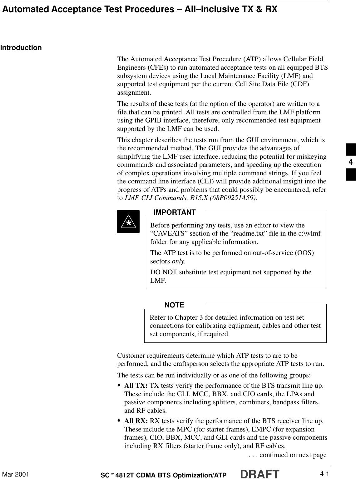
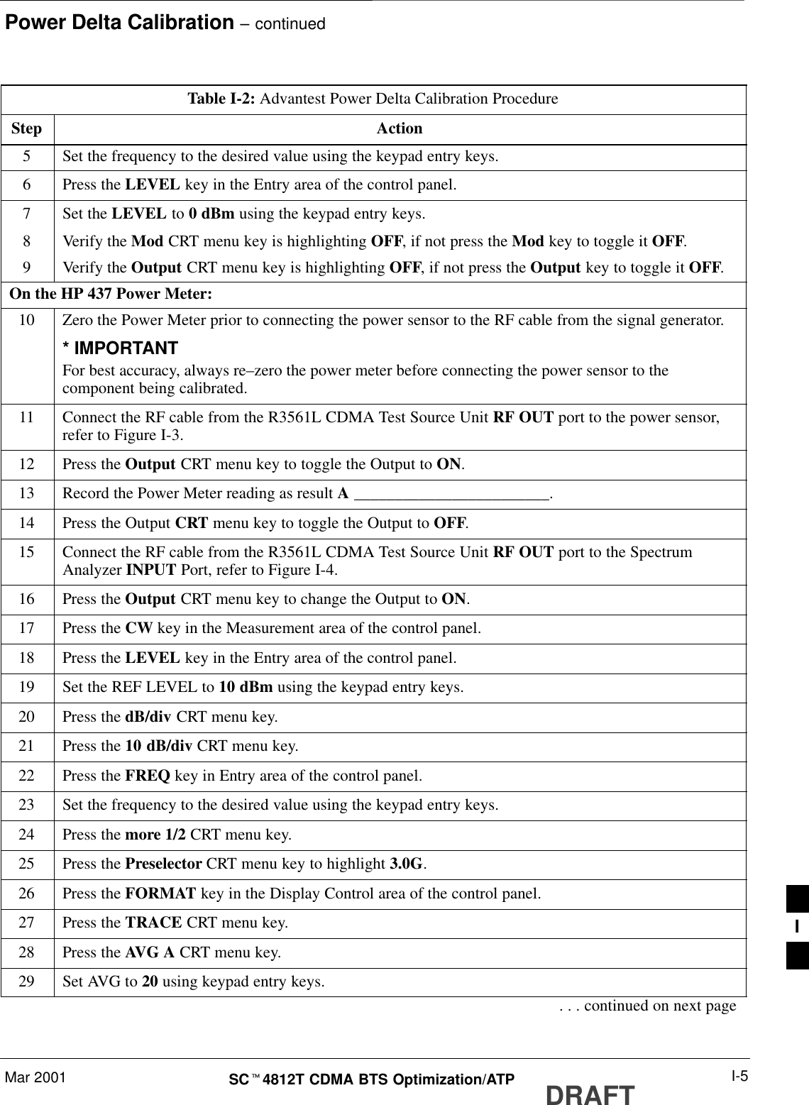
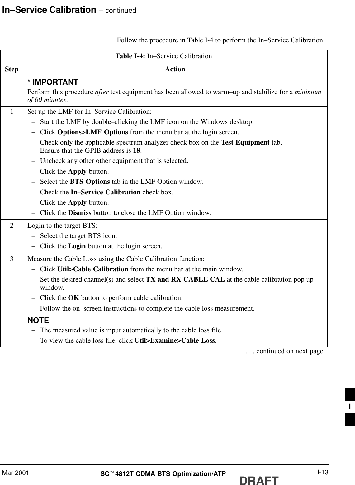
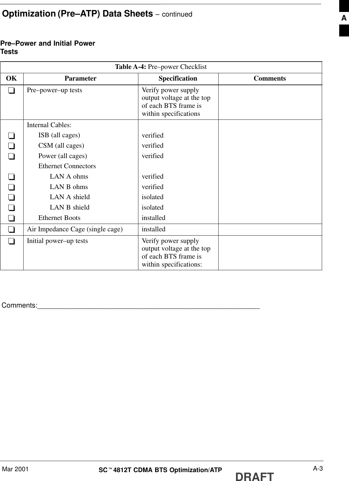
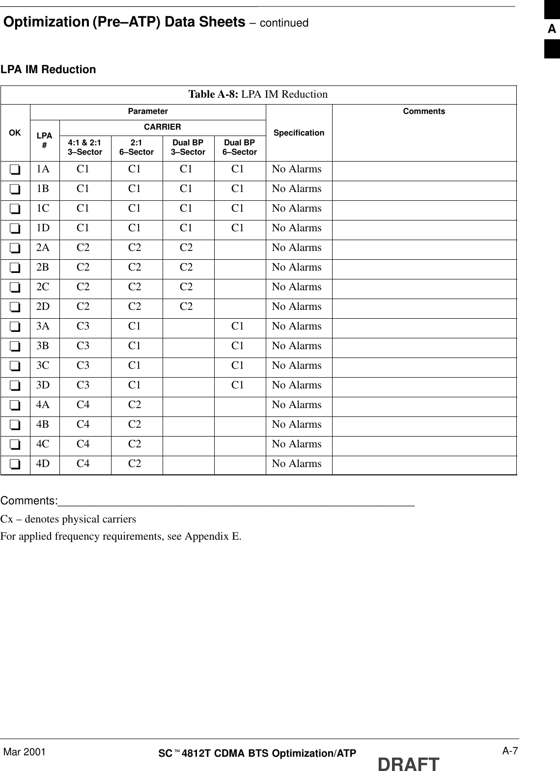
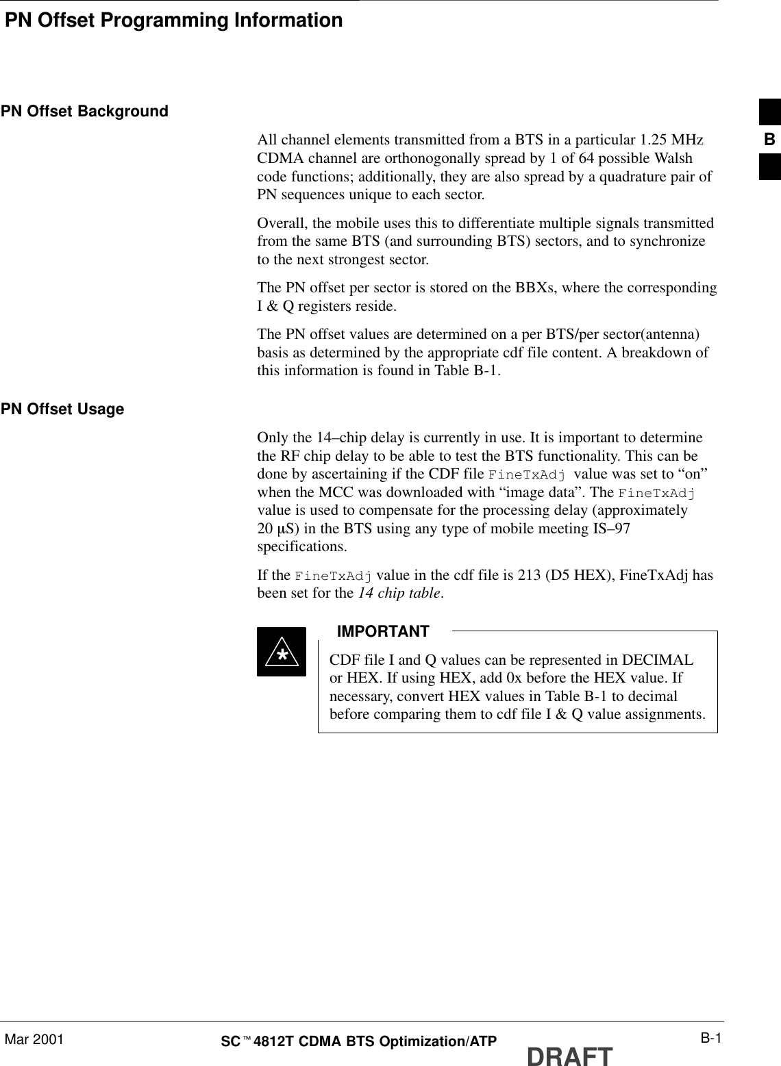
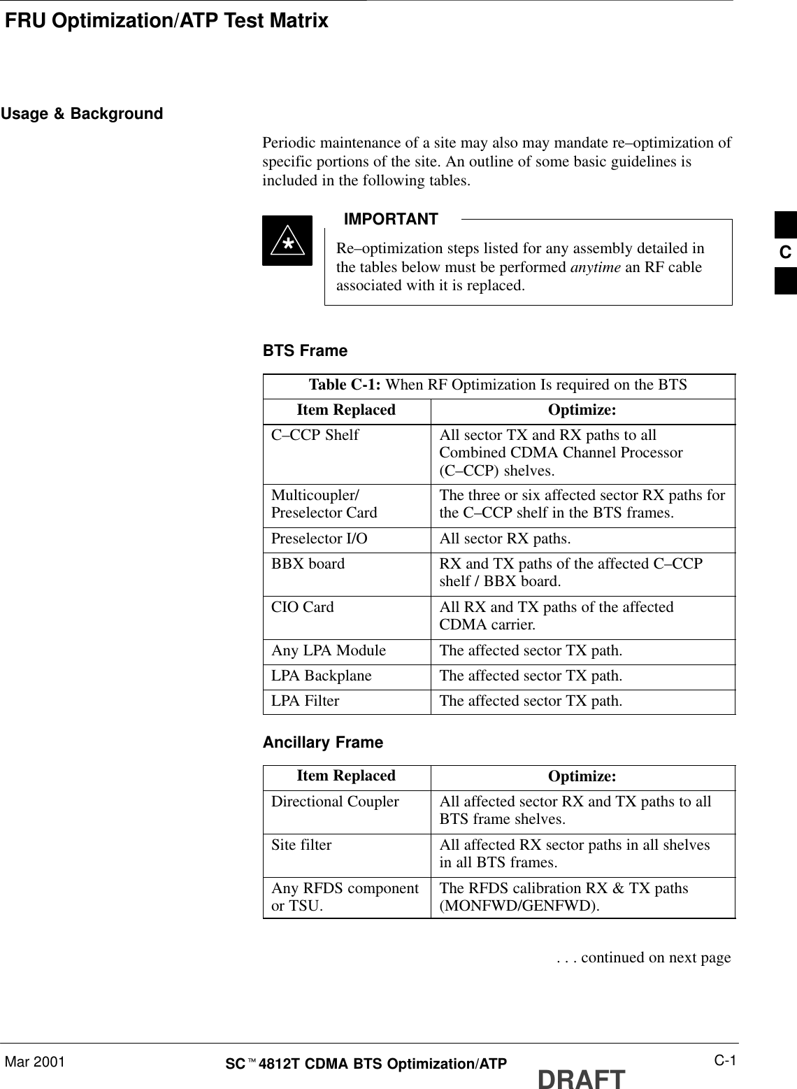
![Automated Acceptance Test Procedure – All–inclusive TX & RX – continuedDRAFTSCt4812T CDMA BTS Optimization/ATP Mar 20014-4Table 4-1: ATP Test ProcedurenActionStep4Enter the appropriate channel number in the Carrier n Channels box.The default channel number displayed is determined by the CdmaChans[n] number in thecbsc–n.cdf file for the BTS.5Click on the OK button.The status report window and a Directions pop-up are displayed.6Follow the cable connection directions as they are displayed.The test results are displayed in the status report window.7Click on Save Results or Dismiss.NOTEIf Dismiss is used, the test results will not be saved in the test report file. 4](https://usermanual.wiki/Nokia-Solutions-and-Networks/T5BL1.IHET5BL1-User-Manual-Part-3-of-3/User-Guide-167768-Page-4.png)
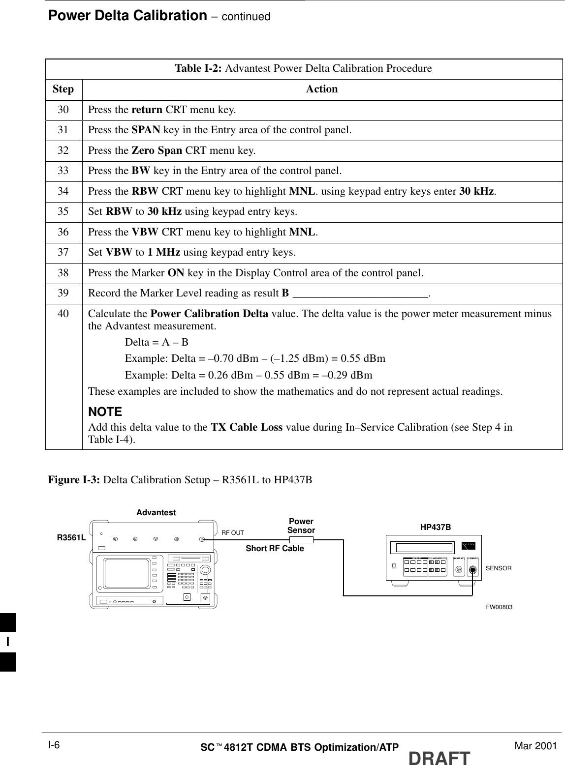
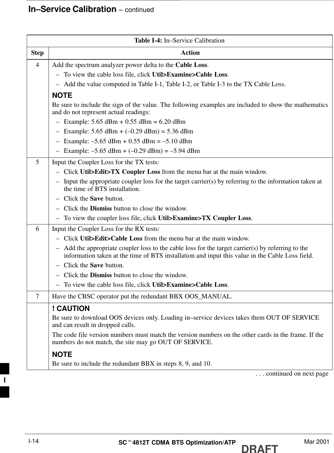
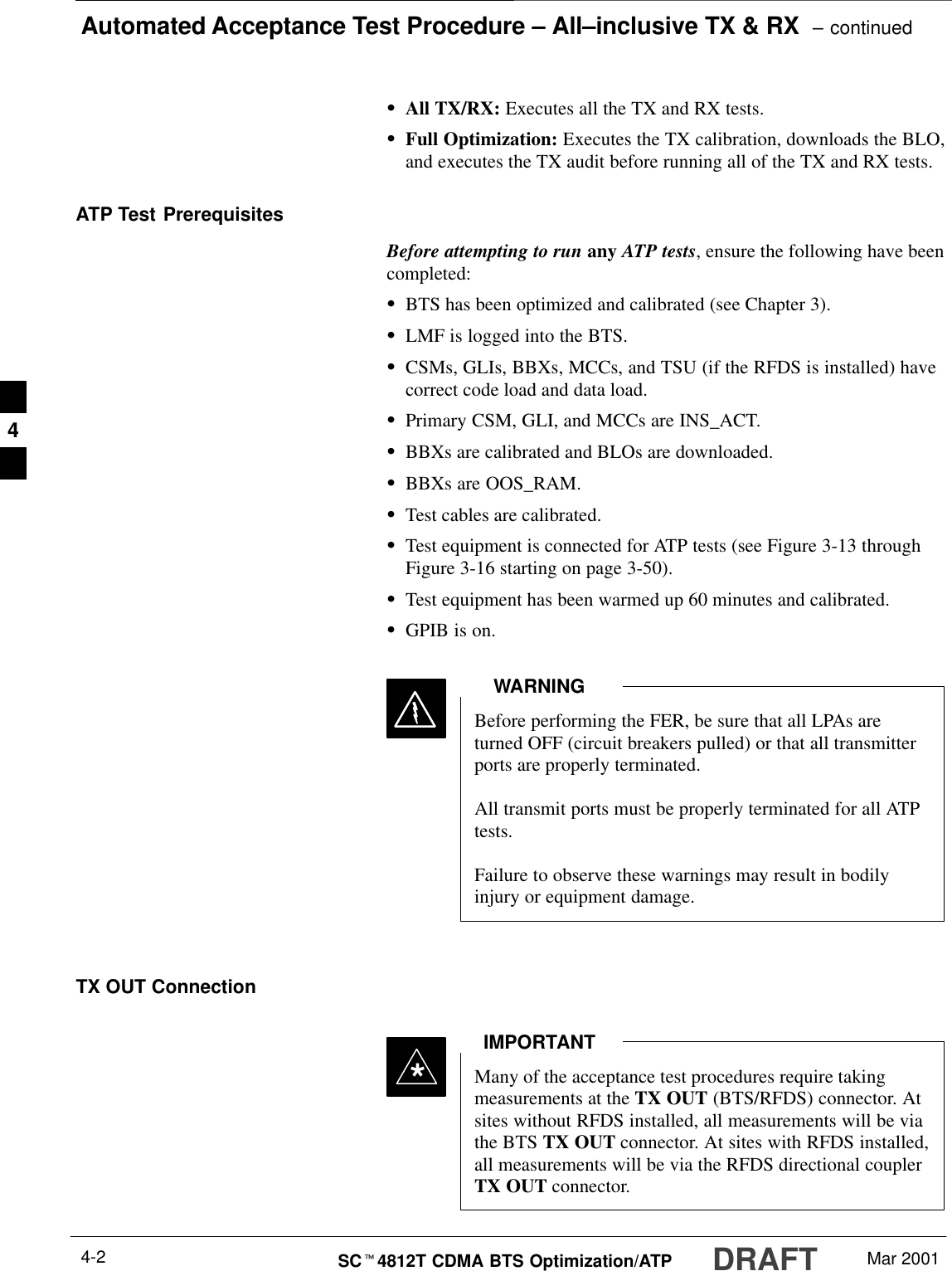
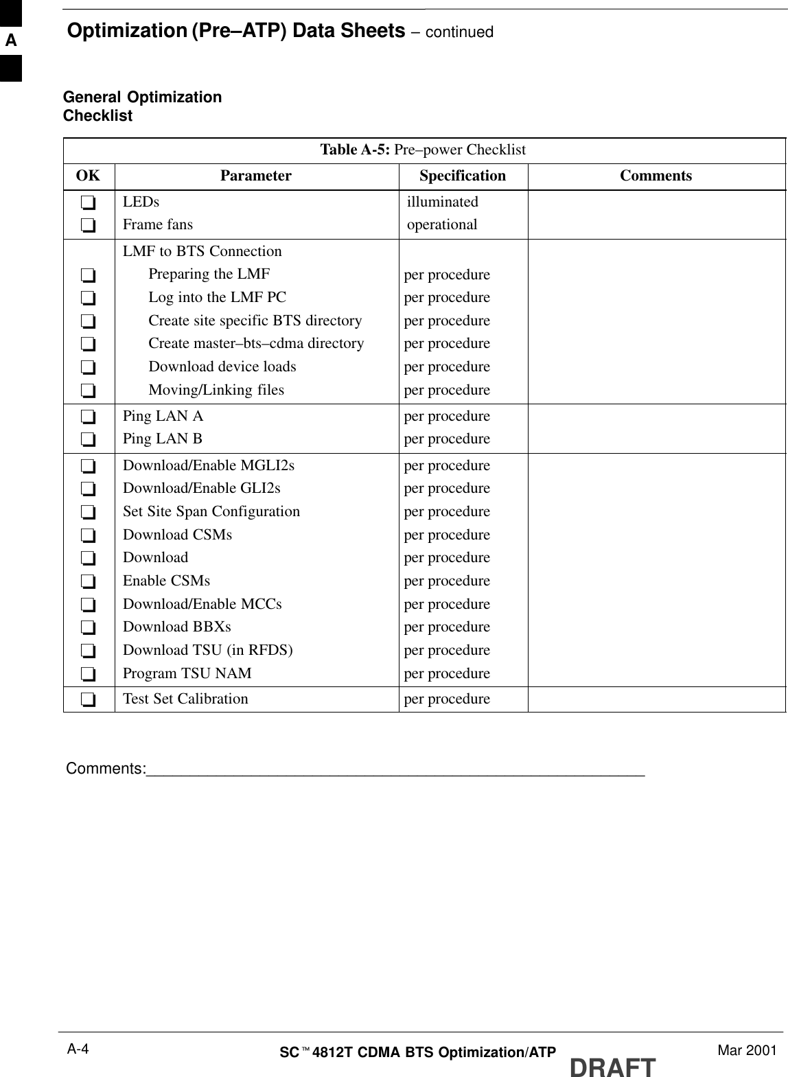
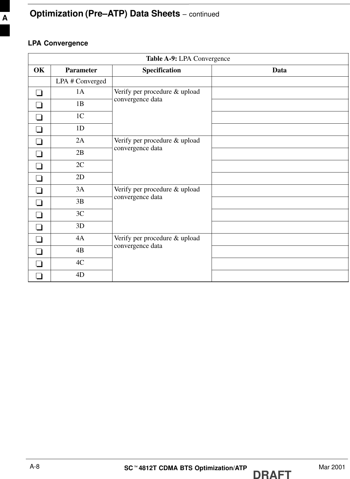
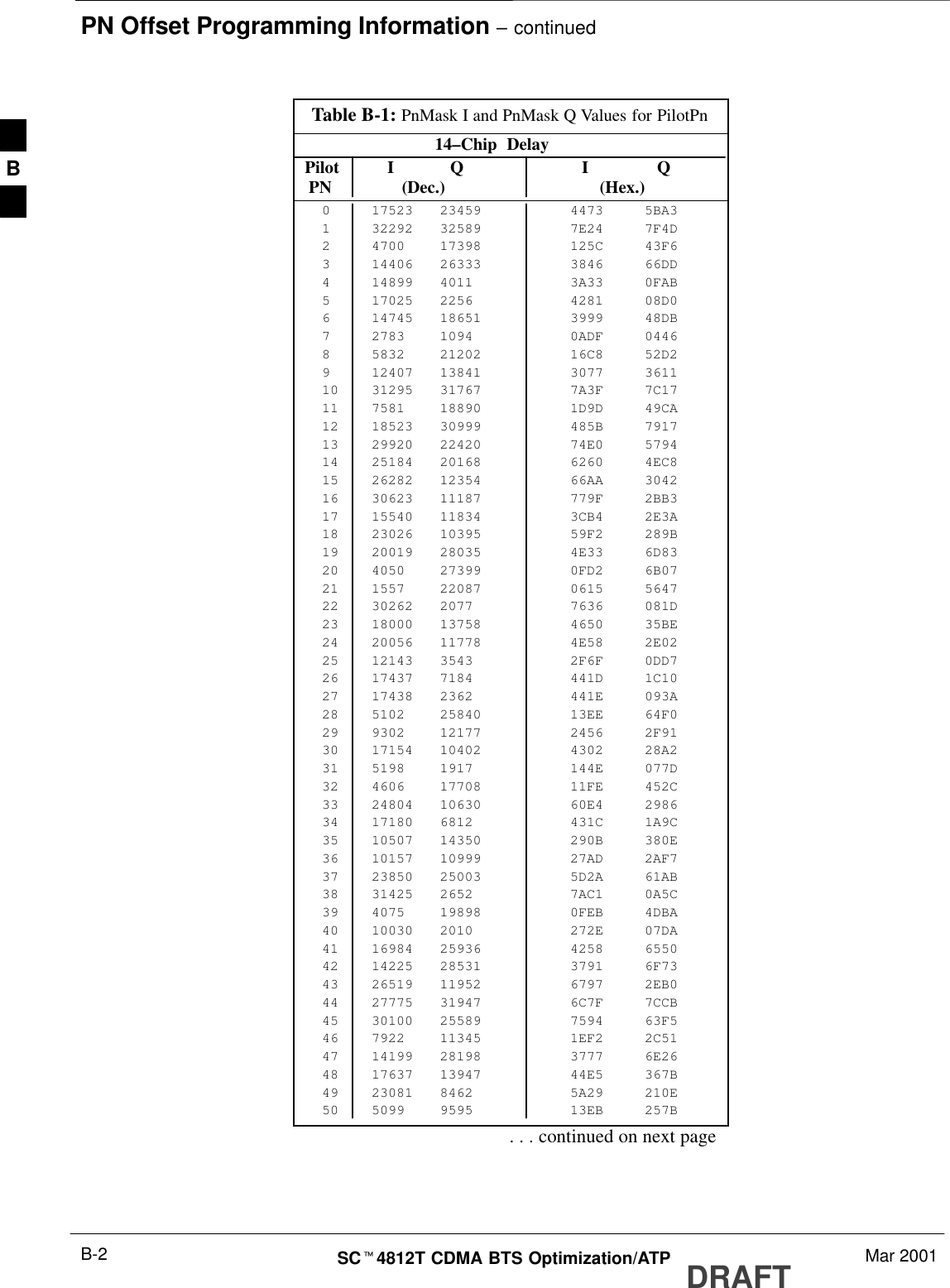
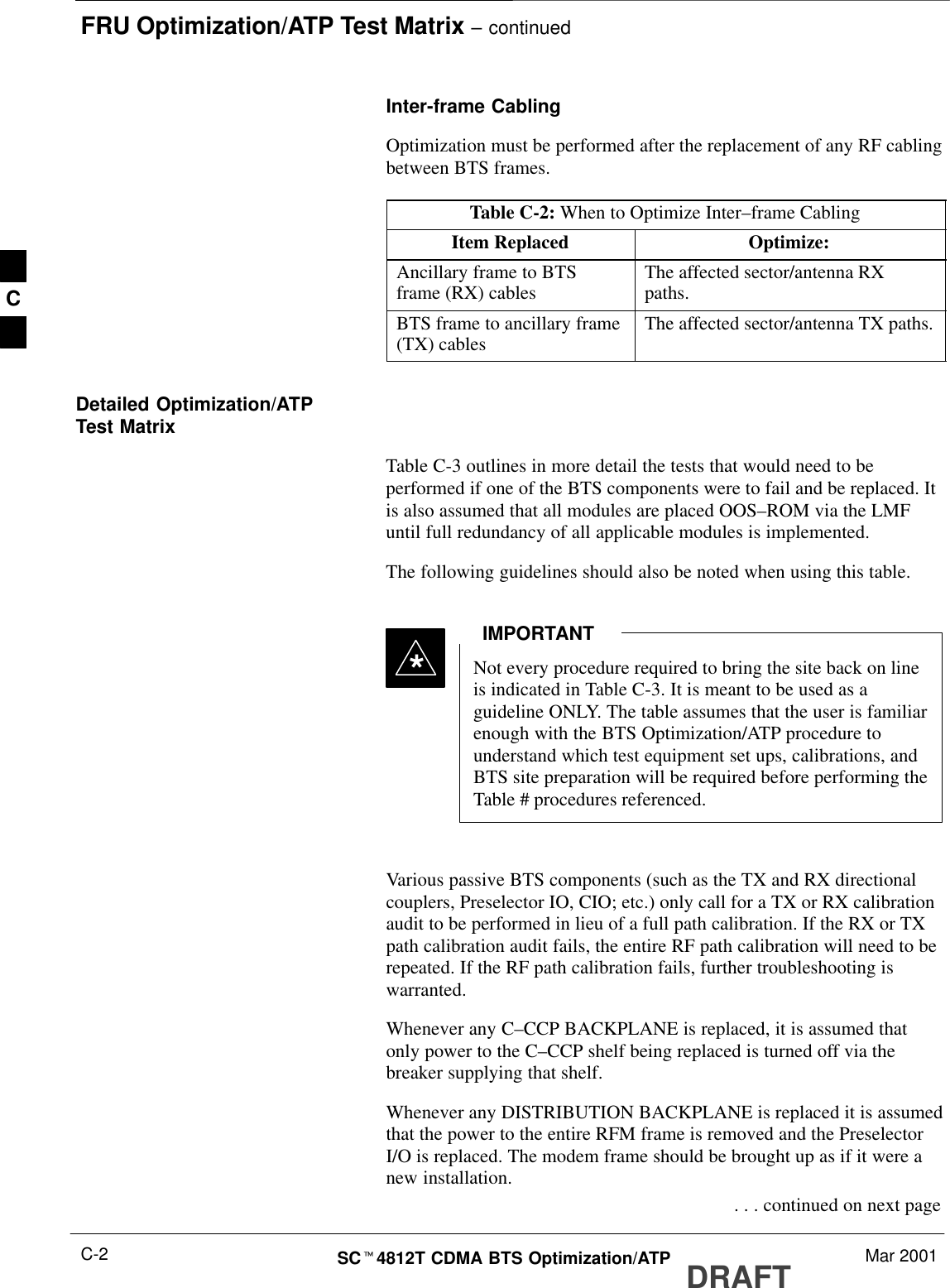
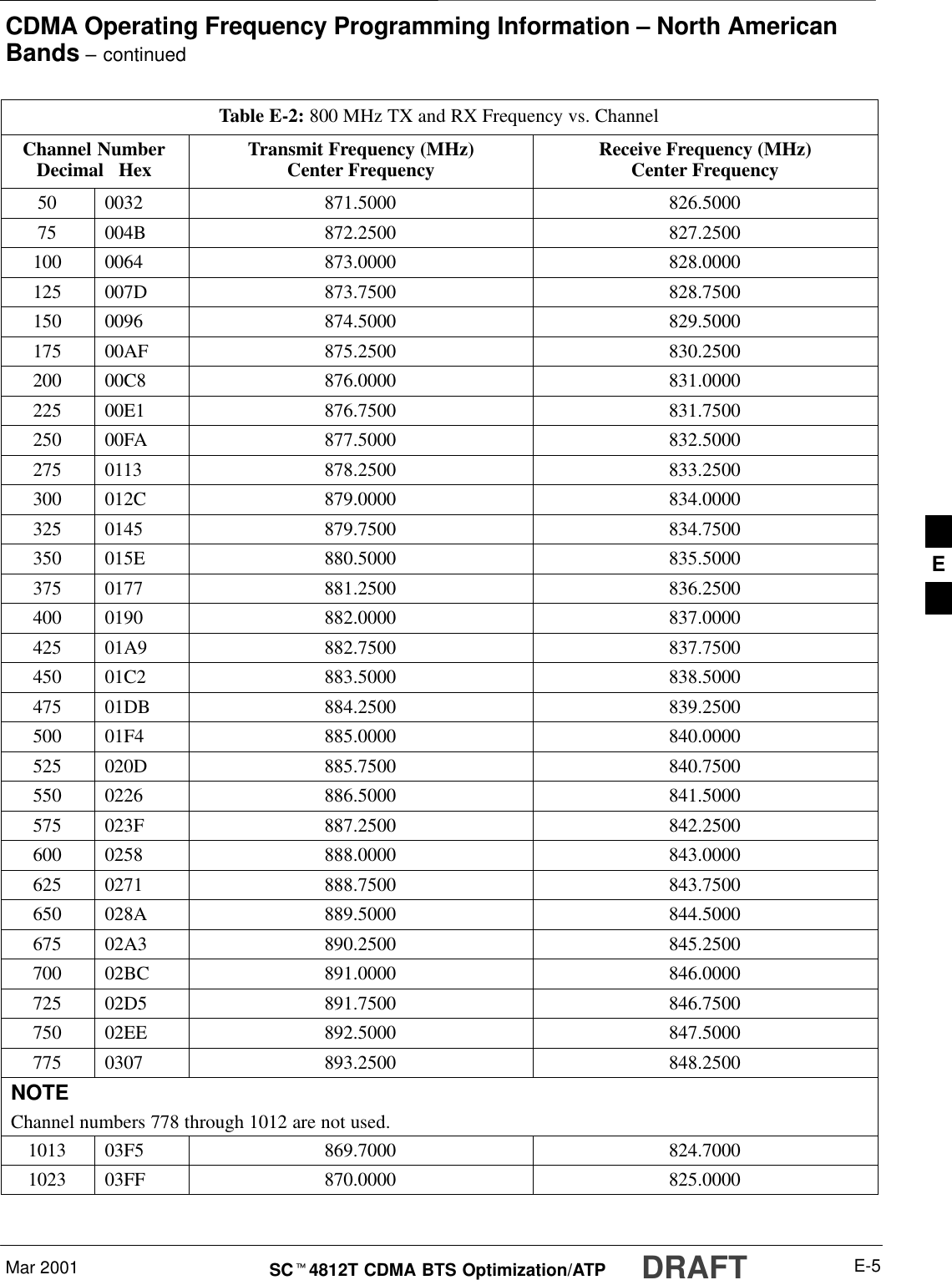
![RX Frame Error Rate (FER) Acceptance TestDRAFTSCt4812T CDMA BTS Optimization/ATP Mar 20014-12FER TestThis test verifies the BTS FER on all traffic channel elements currentlyconfigured on all equipped MCCs (full rate at 1% FER) at an RF inputlevel of –119 dBm [or –116 dBm if using Tower TopAmplifier (TMPC)]. All tests are performed using the external calibratedtest set as the signal source controlled by the same command. Allmeasurements are via the LMF.The Pilot Gain is set to 262 for each TX antenna, and all channelelements from the MCCs are forward-link disabled. The BBX is keyedup, using only bbxlvl level offsets, to generate a CDMA carrier (withpilot channel element only). BBX power output is set to –20 dBm asmeasured at the TX OUT connector (on either the BTS or RFDSdirectional coupler). The BBX must be keyed to enable the RX receivecircuitry.The LMF prompts the MCC/CE under test to measure all zero longcodeand provide the FER report on the selected active MCC on the reverselink for both the main and diversity RX antenna paths, verifying thatresults meet the following specification:SFER returned less than 1% and total frames measured is 1500All MCC/CEs selected are tested on the specified RX antenna path. TheBBX then de-keys and, if selected, the MCC is re-configured to assignthe applicable redundant BBX to the current RX antenna paths undertest. The test is then repeated.4](https://usermanual.wiki/Nokia-Solutions-and-Networks/T5BL1.IHET5BL1-User-Manual-Part-3-of-3/User-Guide-167768-Page-12.png)

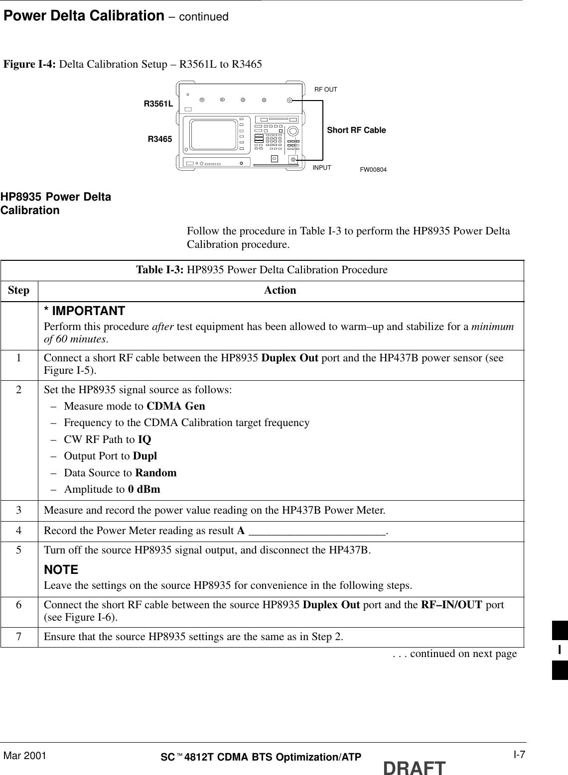
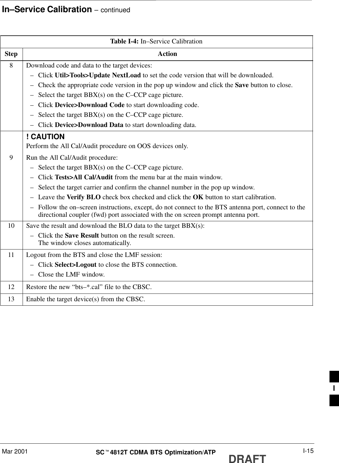
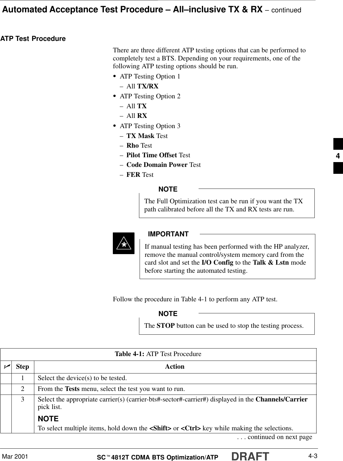
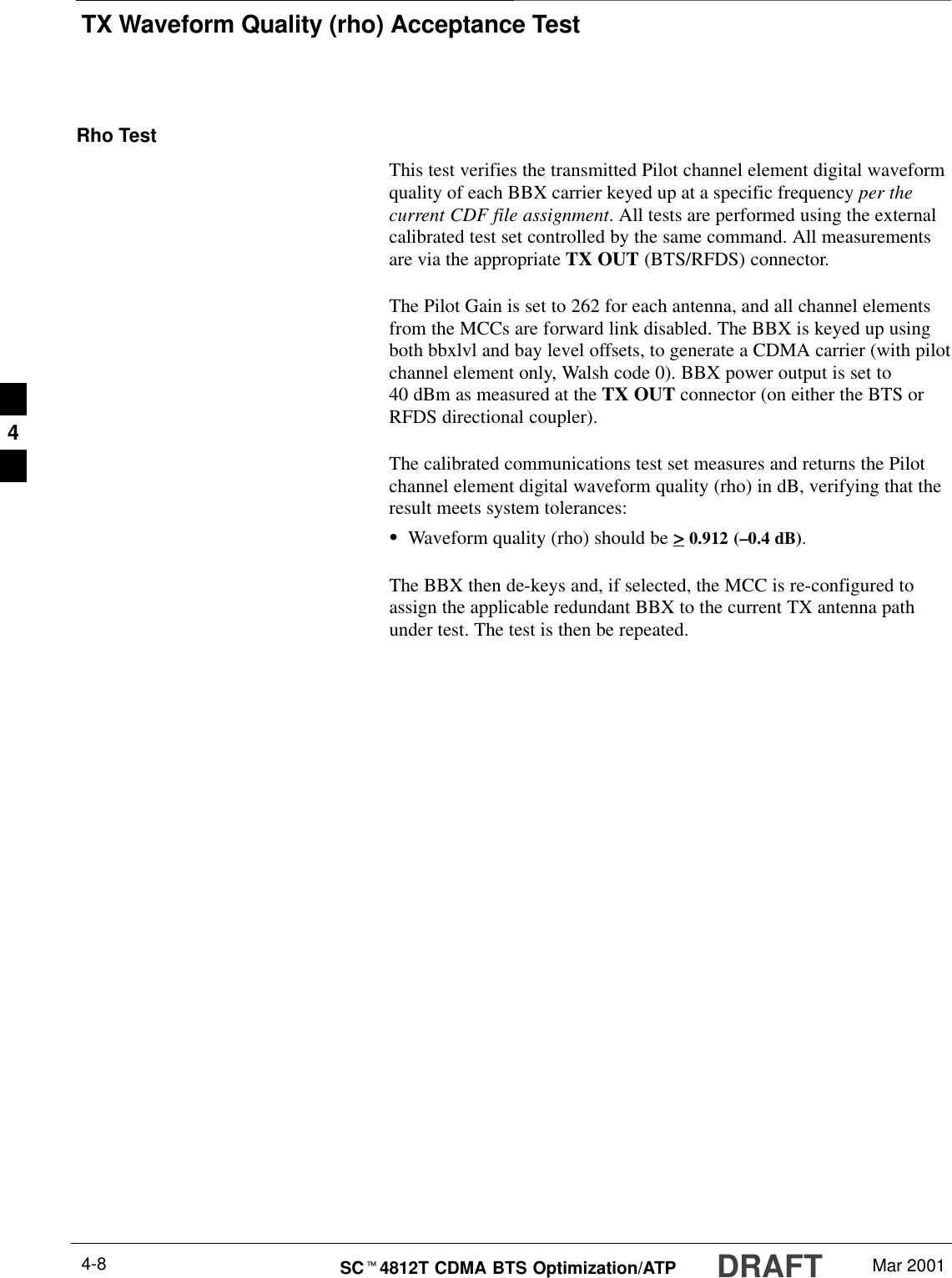
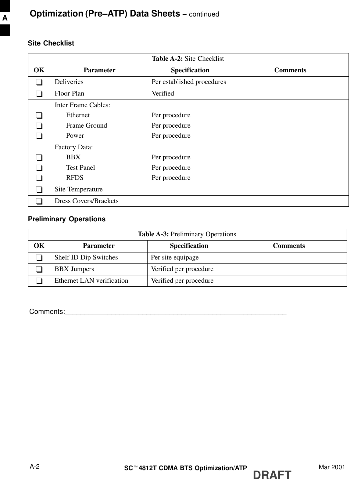
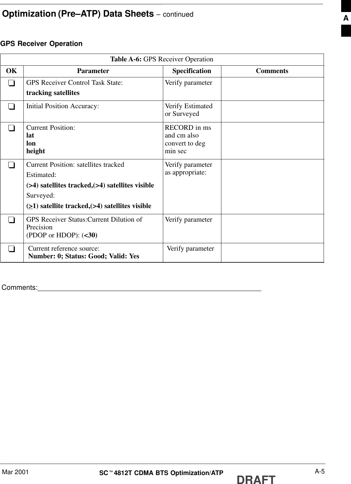
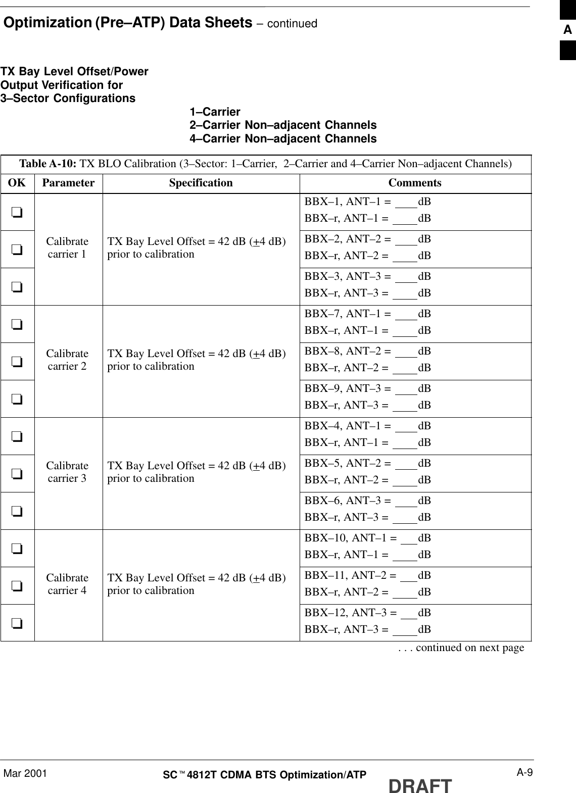
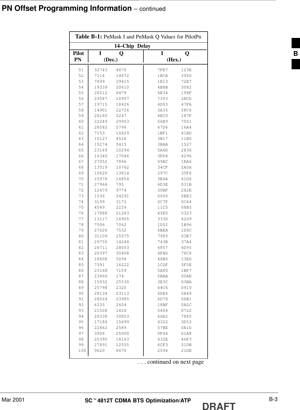
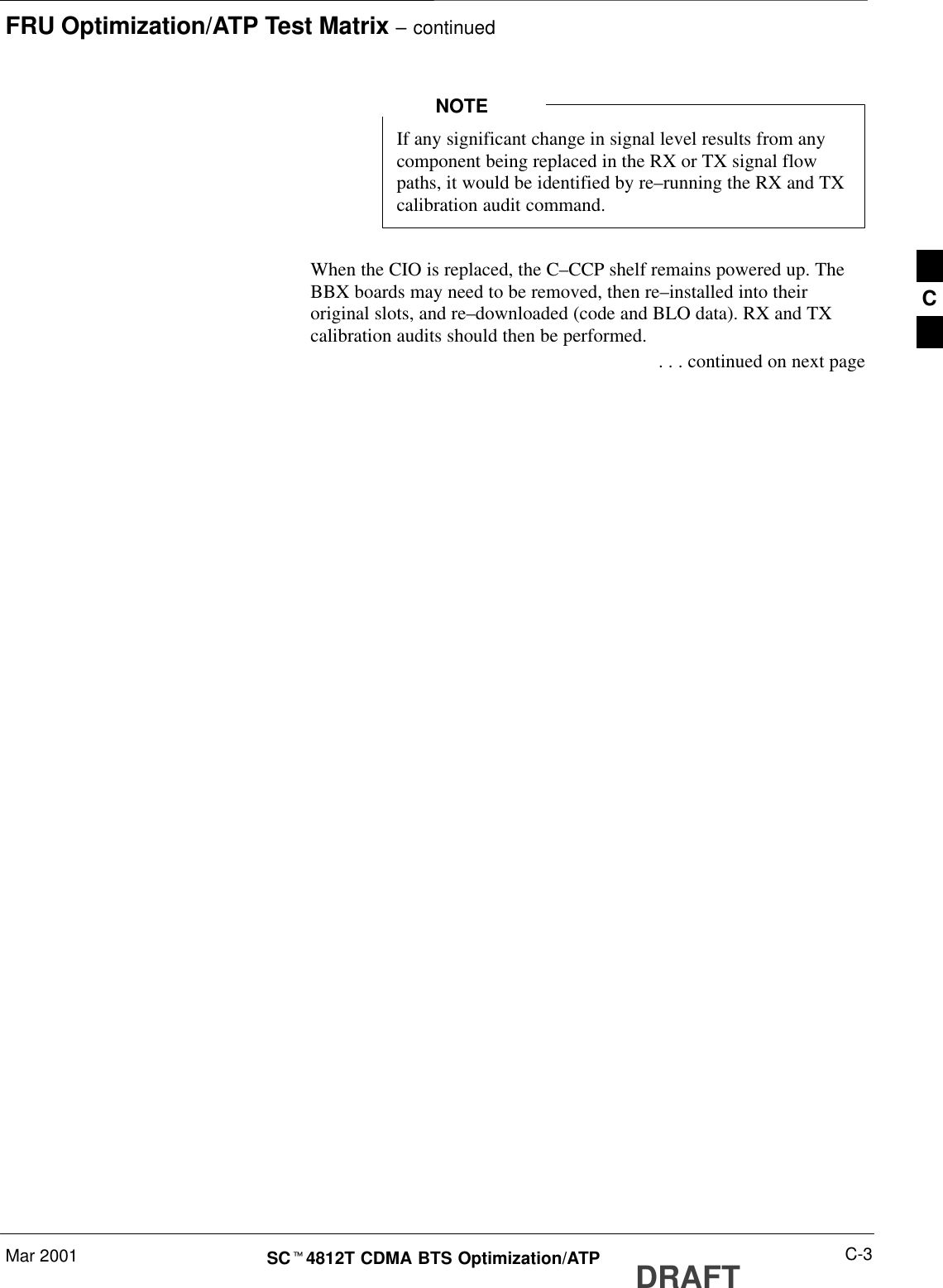
![Troubleshooting: InstallationDRAFTSCt4812T CDMA BTS Optimization/ATP Mar 20016-2Cannot Log into Cell-SiteFollow the procedure in Table 6-1 to troubleshoot a login failure.Table 6-1: Login Failure Troubleshooting ProceduresnStep Action1If MGLI2 LED is solid RED, it implies a hardware failure. Reset MGLI2 by re-seating it. If thispersists, install a known good MGLI2 card in MGLI2 slot and retry. A Red LED may also indicateno Ethernet termination at top of frame.2Verify that T1 is disconnected (see Table 3-1 on page 3-4).If T1 is still connected, verify the CBSC has disabled the BTS.3Try pinging the MGLI2 (see Table 3-6 on page 3-15).4Verify the LMF is connected to the Primary LMF port (LAN A) in the front of the BTS (seeTable 3-2 on page 3-5).5Verify the LMF was configured properly (see Preparing the LMF section starting on page 3–6).6Verify the BTS-LMF cable is RG-58 [flexible black cable of less than 76 cm (2.5 feet) length].7Verify the Ethernet ports are terminated properly (see Figure 3-4 on page 3-14).8Verify a T-adapter is not used on the LMF side port if connected to the BTS front LMF primaryport.9Try connecting to the I/O panel (top of frame). Use BNC T-adapters at the LMF port for thisconnection.10 Re-boot the LMF and retry.11 Re-seat the MGLI2 and retry.12 Verify IP addresses are configured properly.Cannot Communicate toPower MeterFollow the procedure in Table 6-2 to troubleshoot a power metercommunication failure.Table 6-2: Troubleshooting a Power Meter Communication FailurenStep Action1Verify the Power Meter is connected to the LMF with a GPIB adapter.2Verify the cable setup as specified in Chapter 3.3Verify the GPIB address of the Power Meter is set to 13.4Verify the GPIB adapter DIP switch settings are correct.Refer to the Test Equipment setup section for details.. . . continued on next page6](https://usermanual.wiki/Nokia-Solutions-and-Networks/T5BL1.IHET5BL1-User-Manual-Part-3-of-3/User-Guide-167768-Page-30.png)
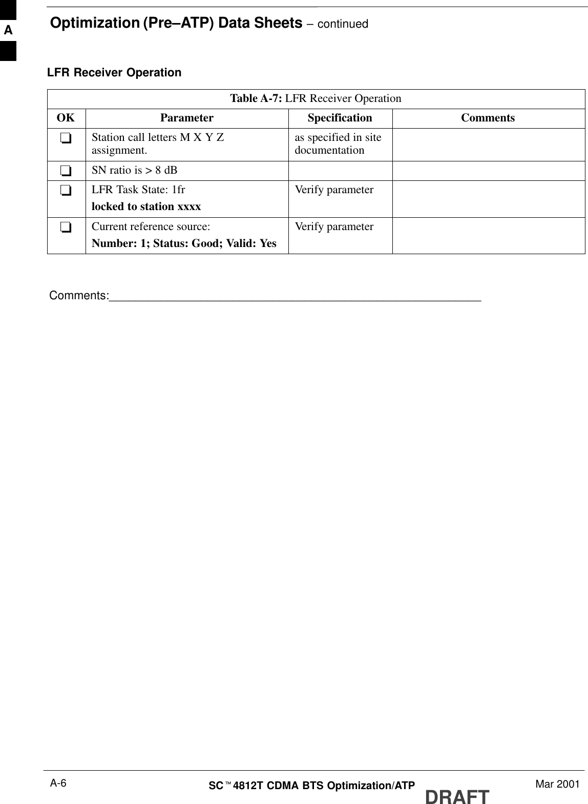
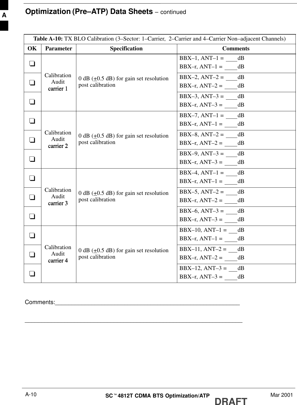


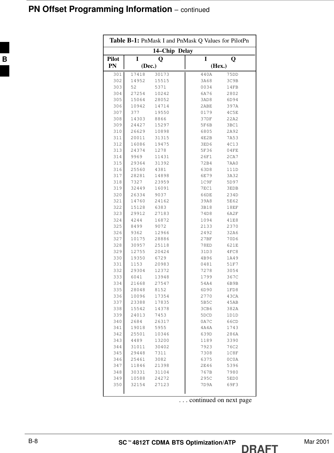


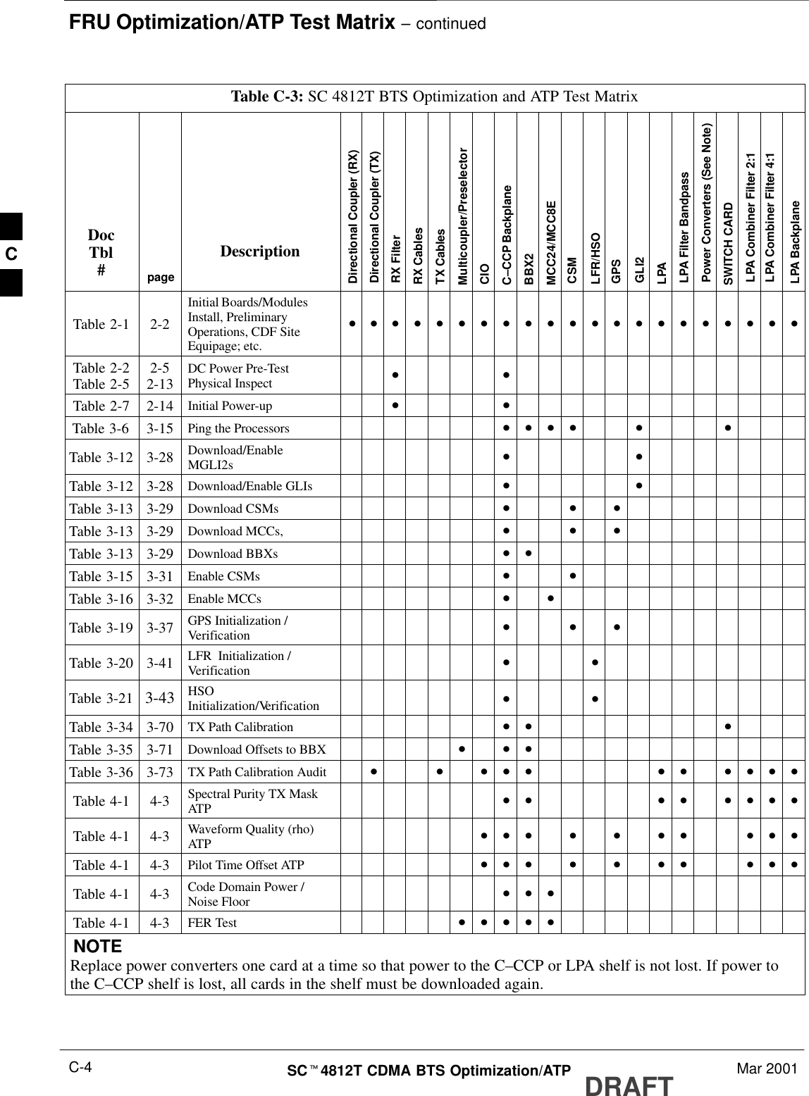


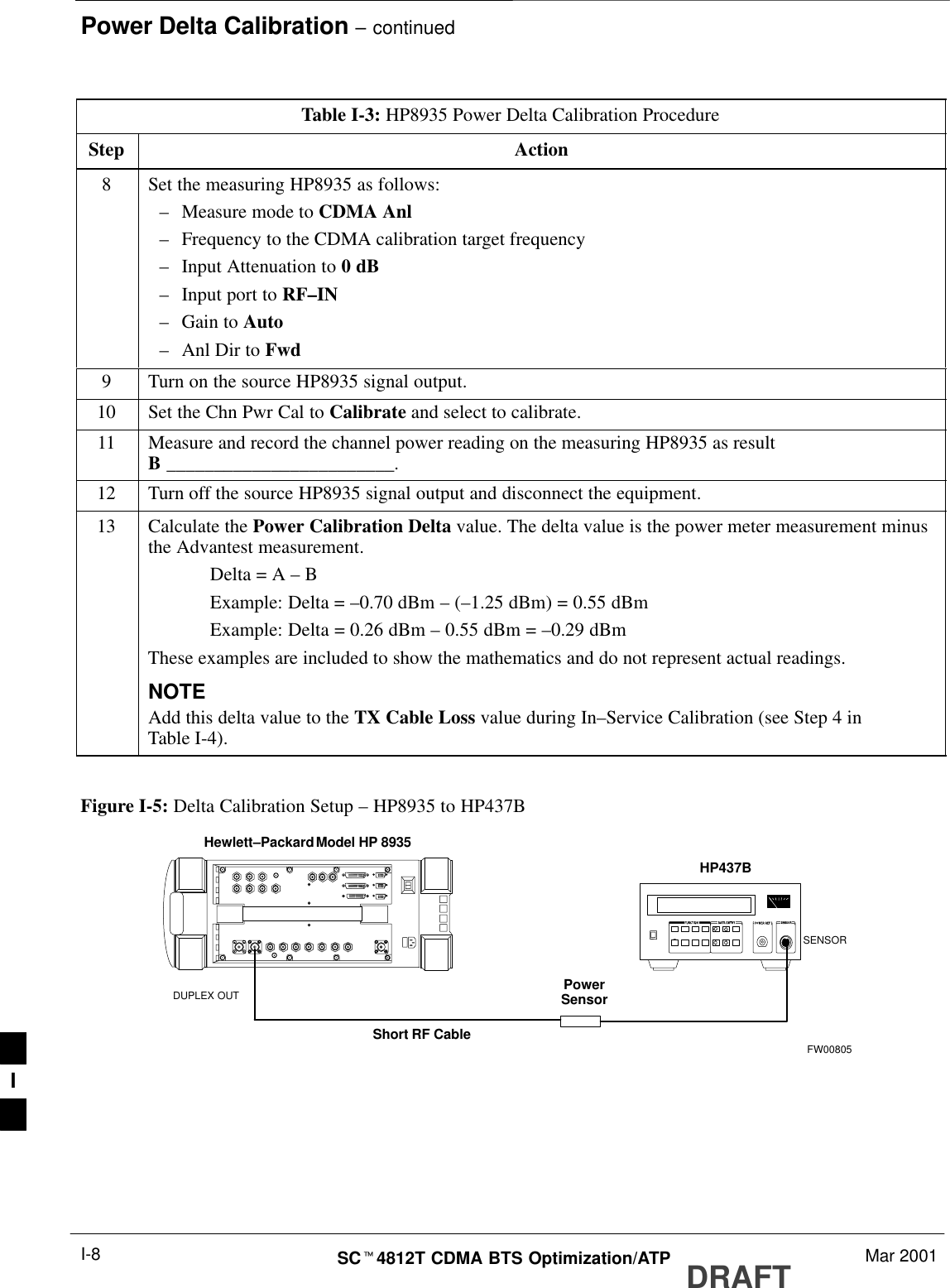
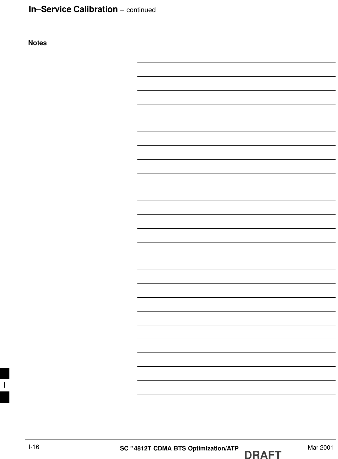
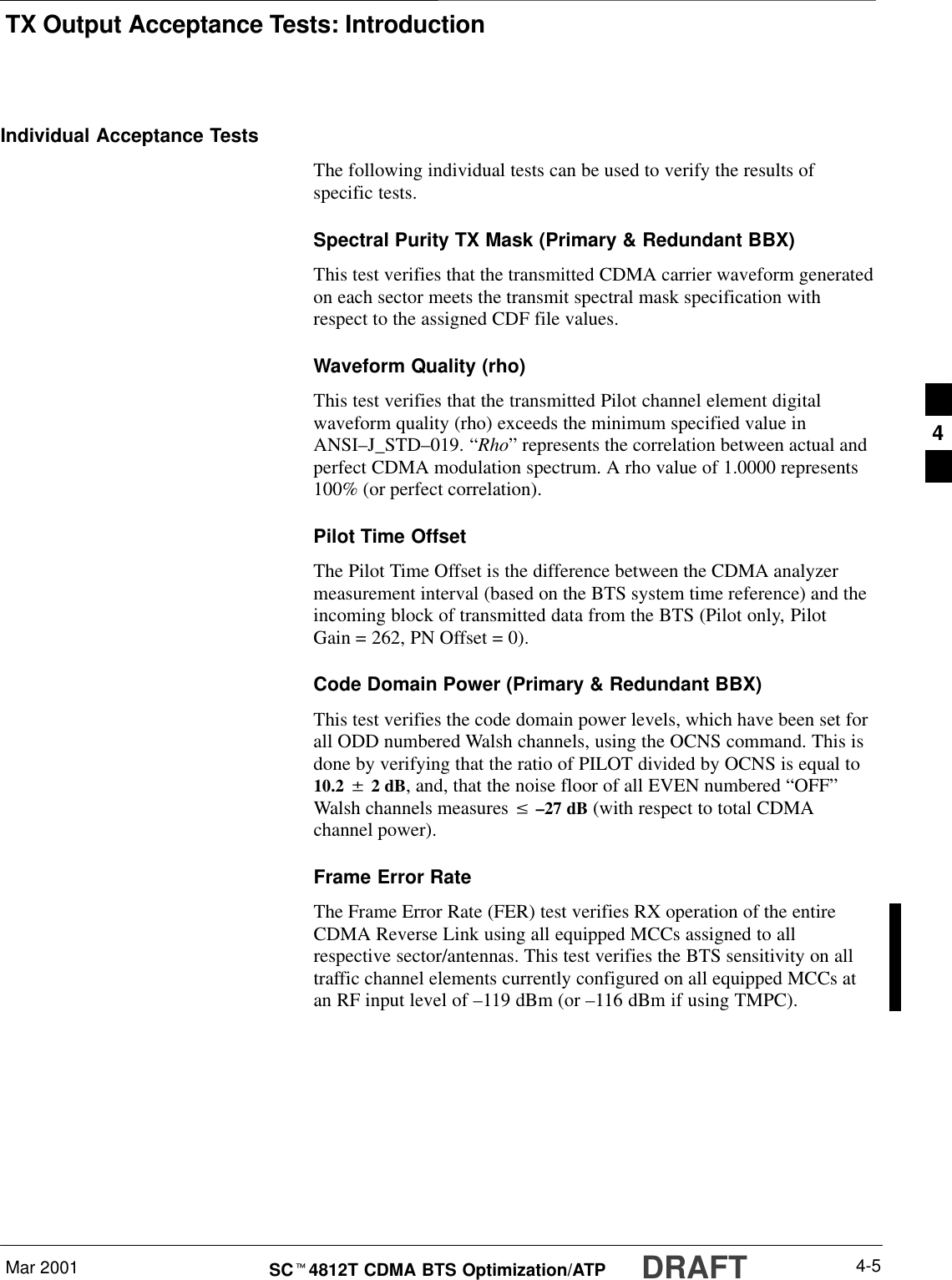
![Test Equipment Setup – continuedDRAFTSCt4812T CDMA BTS Optimization/ATP Mar 2001F-2PrerequisitesPrior to performing any of these procedures, all preparations forpreparing the LMF, updating LMF files, and any other pre-calibrationprocedures, as stated in Chapter 3, must have been completed.HP8921A System ConnectivityTestFollow the steps in Table F-1 to verify that the connections between thePCS Interface and the HP8921A are correct, and cables are intact. Thesoftware also performs basic functionality checks of each instrument.Disconnect other GPIB devices, especially systemcontrollers, from the system before running theconnectivity software.IMPORTANT*Table F-1: System ConnectivityStep Action* IMPORTANT–Perform this procedure after test equipment has been allowed to warm–up and stabilize for aminimum of 60 minutes.1Insert HP 83236A Manual Control/System card into memory card slot.2Press the [PRESET] pushbutton.3Press the Screen Control [TESTS] pushbutton to display the “Tests” Main Menu screen.4Position the cursor at Select Procedure Location and select by pressing the cursor control knob.In the Choices selection box, select Card.5Position the cursor at Select Procedure Filename and select by pressing the cursor control knob.In the Choices selection box, select SYS_CONN.6Position the cursor at RUN TEST and select it.The software will prompt you through the connectivity setup.7When the test is complete, position the cursor on STOP TEST and select it; OR press the [K5]pushbutton.8To return to the main menu, press the [K5] pushbutton.F](https://usermanual.wiki/Nokia-Solutions-and-Networks/T5BL1.IHET5BL1-User-Manual-Part-3-of-3/User-Guide-167768-Page-116.png)
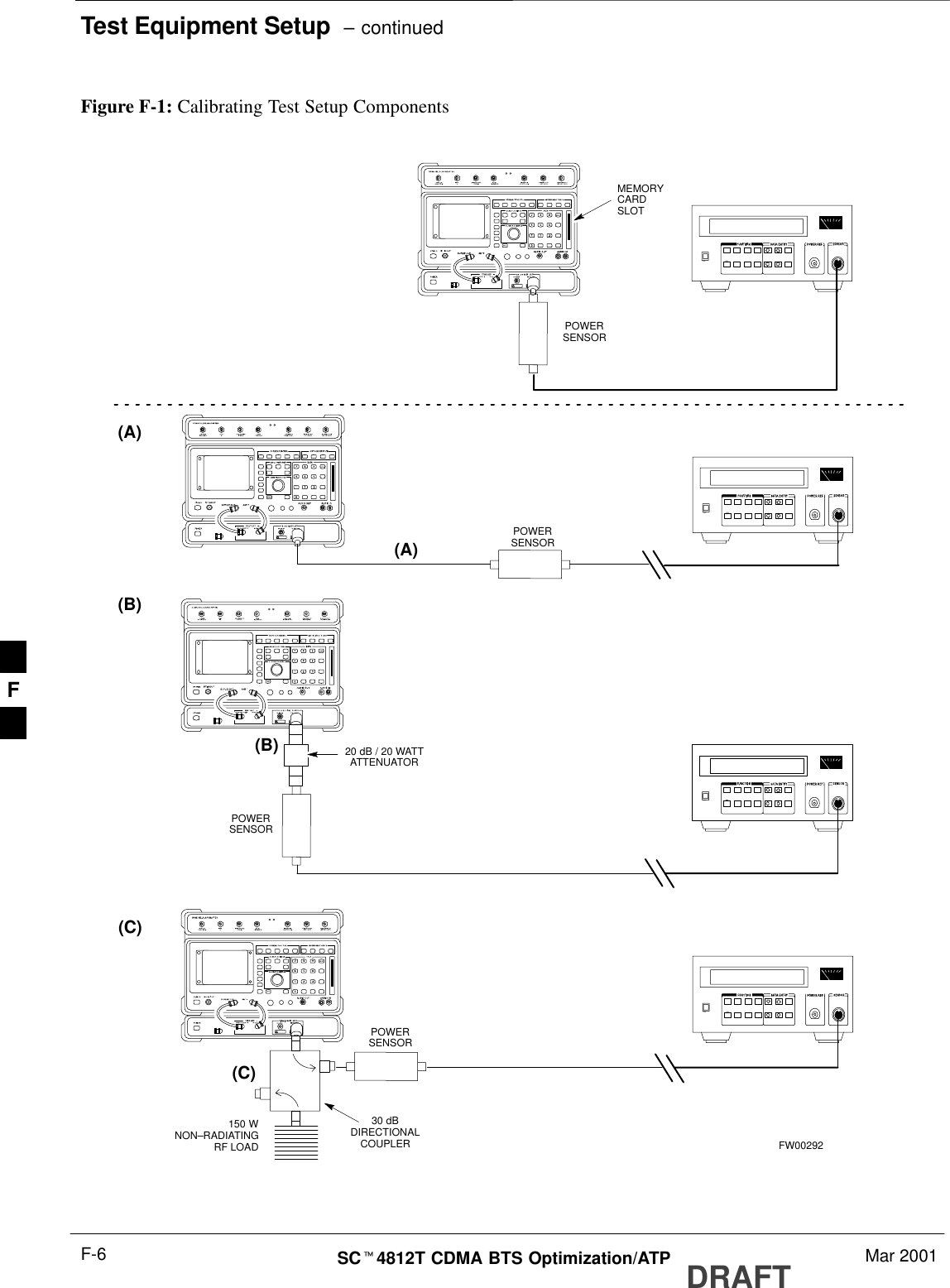
![Test Equipment Setup – continuedMar 2001 F-3SCt4812T CDMA BTS Optimization/ATP DRAFTManual Cable Calibrationusing HP8921 with HP PCS Interface (HP83236)Perform the procedure in Table F-2 to calibrate the test equipment usingthe HP8921 Cellular Communications Analyzer equipped with theHP83236 PCS Interface.This calibration method must be executed with great care.Some losses are measured close to the minimum limit ofthe power meter sensor (–30 dBm).NOTEPrerequisitesEnsure the following prerequisites have been met before proceeding:STest equipment to be calibrated has been connected correctly for cablecalibration.STest equipment has been selected and calibrated.Refer to Figure F-1 for location of the components on the PCS Interfaceand Communications Test Set.Table F-2: Manual Cable Calibration Test Equipment Setup (using the HP PCS Interface)Step ActionNOTEVerify that GPIB controller is turned off.1Insert HP 83236A Manual Control System card into memory card slot (see Figure F-1).2Press the Preset pushbutton.3 Under Screen Controls, press the TESTS pushbutton to display the TESTS (Main Menu) screen.4Position the cursor at Select Procedure Location and select it. In the Choices selection box, selectCARD.5Position the cursor at Select Procedure Filename and select it. In the Choices selection box, selectMANUAL.6Position the cursor at RUN TEST and select it. HP must be in Control Mode Select YES.7If using HP 83236A:Set channel number=<chan#>:–Position cursor at ChannelNumber and select it.–Enter the chan# using the numerickeypad; press [Enter] and thescreen will go blank.–When the screen reappears, thechan# will be displayed on thechannel number line.If using HP 83236B:Set channel frequency:–Position cursor at Frequency Band and press Enter.–Select User Defined Frequency.–Go Back to Previous Menu.–Position the cursor to 83236 generator frequency andenter actual RX frequency.–Position the cursor to 83236 analyzer frequency andenter actual TX frequency.. . . continued on next pageF](https://usermanual.wiki/Nokia-Solutions-and-Networks/T5BL1.IHET5BL1-User-Manual-Part-3-of-3/User-Guide-167768-Page-117.png)
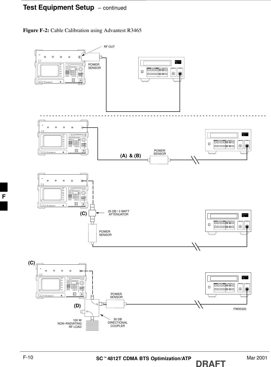
![Test Equipment Setup – continuedDRAFTSCt4812T CDMA BTS Optimization/ATP Mar 2001F-4Table F-2: Manual Cable Calibration Test Equipment Setup (using the HP PCS Interface)Step Action8Set RF Generator level:–Position the cursor at RF Generator Level and select it.–Enter –10 using the numeric keypad; press [Enter] and the screen will go blank.–When the screen reappears, the value –10 dBm will be displayed on the RF Generator Level line.9Set the user fixed Attenuation Setting to 0 dBm:–Position cursor at Analyzer Attenuation and select it–Position cursor at User Fixed Atten Settings and select it.–Enter 0 (zero) using the numeric keypad and press [Enter].10 Select Back to Previous Menu.11 Record the HP83236 Generator Frequency Level:Record the HP83236B Generator Frequency Level:–Position cursor at Show Frequency and Level Details and select it.–Under HP83236 Frequencies and Levels, record the Generator Level.–Under HP83236B Frequencies and Levels, record the Generator Frequency Level(1850 – 1910 MHz for 1.9 GHz or 1750 – 1780 for 1.7 GHz).–Position cursor at Prev Menu and select it.12 Click on Pause for Manual Measurement.13 Connect the power sensor directly to the RF OUT ONLY port of the PCS Interface.14 On the HP8921A, under To Screen, select CDMA GEN.15 Move the cursor to the Amplitude field and click on the Amplitude value.16 Increase the Amplitude value until the power meter reads 0 dBm ±0.2 dB.NOTEThe Amplitude value can be increased coarsely until 0 dBM is reached; then fine tune the amplitudeby adjusting the Increment Set to 0.1 dBm and targeting in on 0 dBm.17 Disconnect the power sensor from the RF OUT ONLY port of the PCS Interface.* IMPORTANTThe Power Meter sensor’s lower limit is –30 dBm. Thus, only components having losses ≤30 dBshould be measured using this method. For further accuracy, always re-zero the power meterbefore connecting the power sensor to the component being calibrated. After connecting thepower sensor to the component, record the calibrated loss immediately.18 Disconnect all components in the test setup and calibrate each one separately by connecting eachcomponent, one-at-a-time, between the RF OUT ONLY PORT and the power sensor (see Figure F-1,Setups A, B, or C). Record the calibrated loss value displayed on the power meter.SExample: (A) Test Cable(s) = –1.4 dB(B) 20 dB Attenuator = –20.1 dB(B) Directional Coupler = –29.8 dB. . . continued on next pageF](https://usermanual.wiki/Nokia-Solutions-and-Networks/T5BL1.IHET5BL1-User-Manual-Part-3-of-3/User-Guide-167768-Page-118.png)
![Test Equipment Setup – continuedMar 2001 F-5SCt4812T CDMA BTS Optimization/ATP DRAFTTable F-2: Manual Cable Calibration Test Equipment Setup (using the HP PCS Interface)Step Action19 After all components are calibrated, reassemble all components together and calculate the total testsetup loss by adding up all the individual losses:SExample: Total test setup loss = –1.4 –29.8 –20.1 = –51.3 dB.This calculated value will be used in the next series of tests.20 Under Screen Controls press the TESTS button to display the TESTS (Main Menu) screen.21 Select Continue (K2).22 Select RF Generator Level and set to –119 dBm.23 Click on Pause for Manual Measurement.24 Verify the HP8921A Communication Analyzer/83203A CDMA interface setup is as follows (fieldsnot indicated remain at default):SVerify the GPIB (HP–IB) address:–under To Screen, select More–select IO CONFIG–Set HP–IB Adrs to 18–set Mode to Talk&LstnSVerify the HP8921A is displaying frequency (instead of RF channel)–Press the blue [SHIFT] button, then press the Screen Control [DUPLEX] button; this switches tothe CONFIG (CONFIGURE) screen.–Use the cursor control to set RF Display to Freq25 Refer to Table 3-29 for assistance in manually setting the cable loss values into the LMF. F](https://usermanual.wiki/Nokia-Solutions-and-Networks/T5BL1.IHET5BL1-User-Manual-Part-3-of-3/User-Guide-167768-Page-119.png)
![Test Equipment Setup – continuedMar 2001 F-7SCt4812T CDMA BTS Optimization/ATP DRAFTHP PCS Interface Test EquipmentSetup for Manual TestingFollow the procedure in Table F-3 to setup the HP PCS Interface Box formanual testing.Table F-3: HP PCS Interface Test Equipment Setup for Manual TestingnStep ActionNOTEVerify GPIB controller is turned off.1Insert HP83236B Manual Control/System card into the memory card slot.2 Under Screen Controls, press the [TESTS] push-button to display the TESTS (Main Menu)screen.3Position the cursor at Select Procedure Location and select. In the Choices selection box, selectCARD.4Position the cursor at Select Procedure Filename and select. In the Choices selection box, selectMANUAL.5Position the cursor at RUN TEST and select OR press the K1 push-button.6Set channel number=<chan#>:–Position cursor at Channel Number and select.–Enter the chan# using the numeric keypad and then press [Enter] (the screen will blank).–When the screen reappears, the chan# will be displayed on the channel number line.* IMPORTANTIf using a TMPC with Tower Top Amplifier (TTA) skip Step 7.7SSet RF Generator level= –119 dBm + Cal factorExample: –119 dBm + 2 dB = –117 dBmSContinue with Step 9 (skip Step 8).8Set RF Generator level= –116 dBm + Cal factor.Example: –116 dBm + 2 dB = –114 dBm9Set the user fixed Attenuation Setting to 0 dB:–Position cursor at RF Generator Level and select.–Position cursor at User Fixed Atten Settings and select.–Enter 0 (zero) using the numeric keypad and press [Enter].10 Select Back to Previous Menu.11 Select Quit, then select Yes.F](https://usermanual.wiki/Nokia-Solutions-and-Networks/T5BL1.IHET5BL1-User-Manual-Part-3-of-3/User-Guide-167768-Page-121.png)