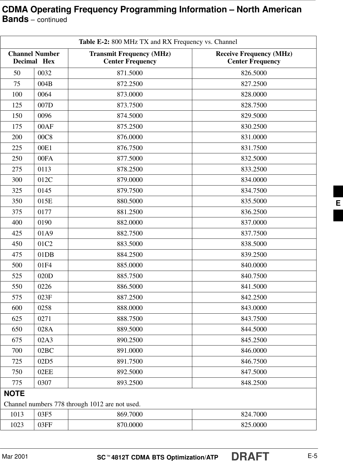
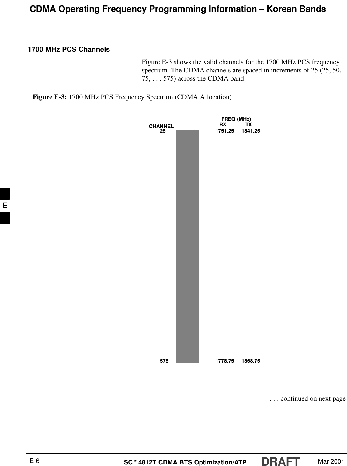
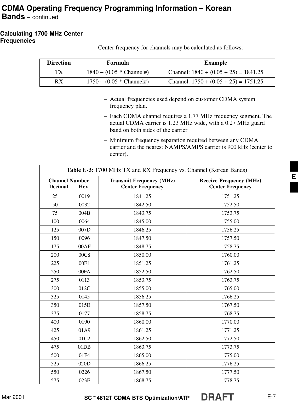
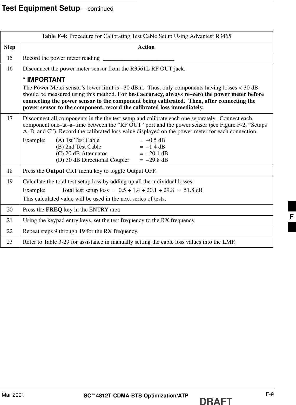
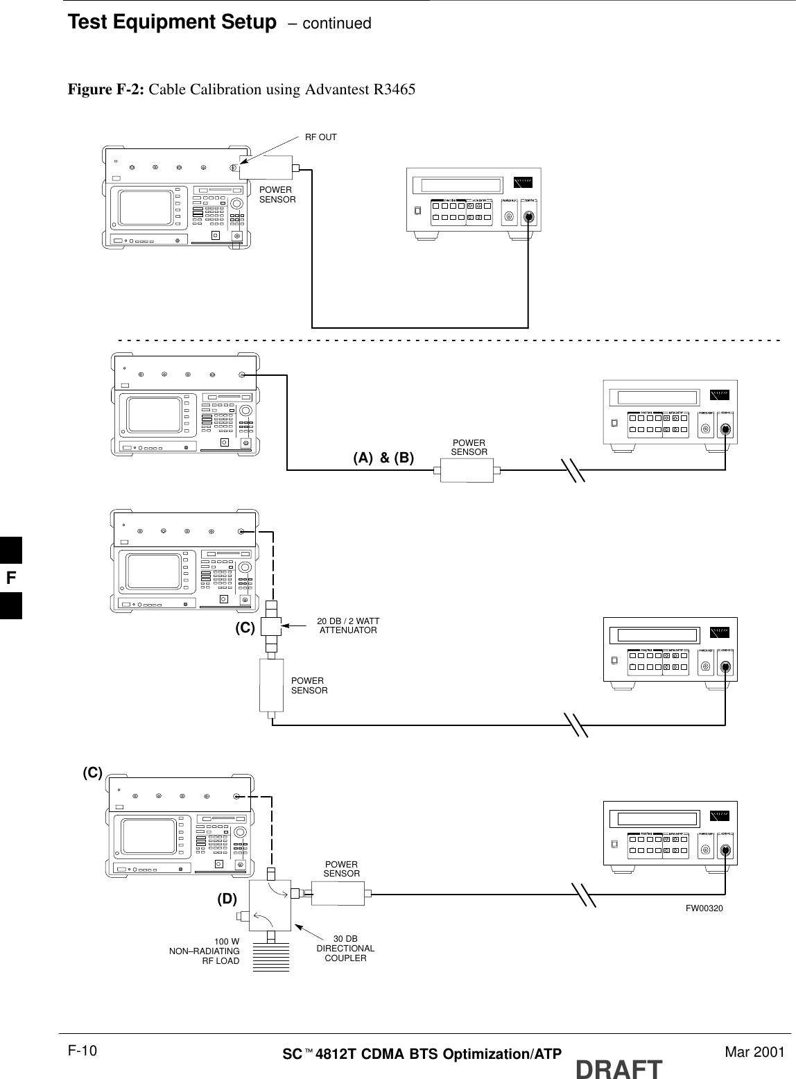
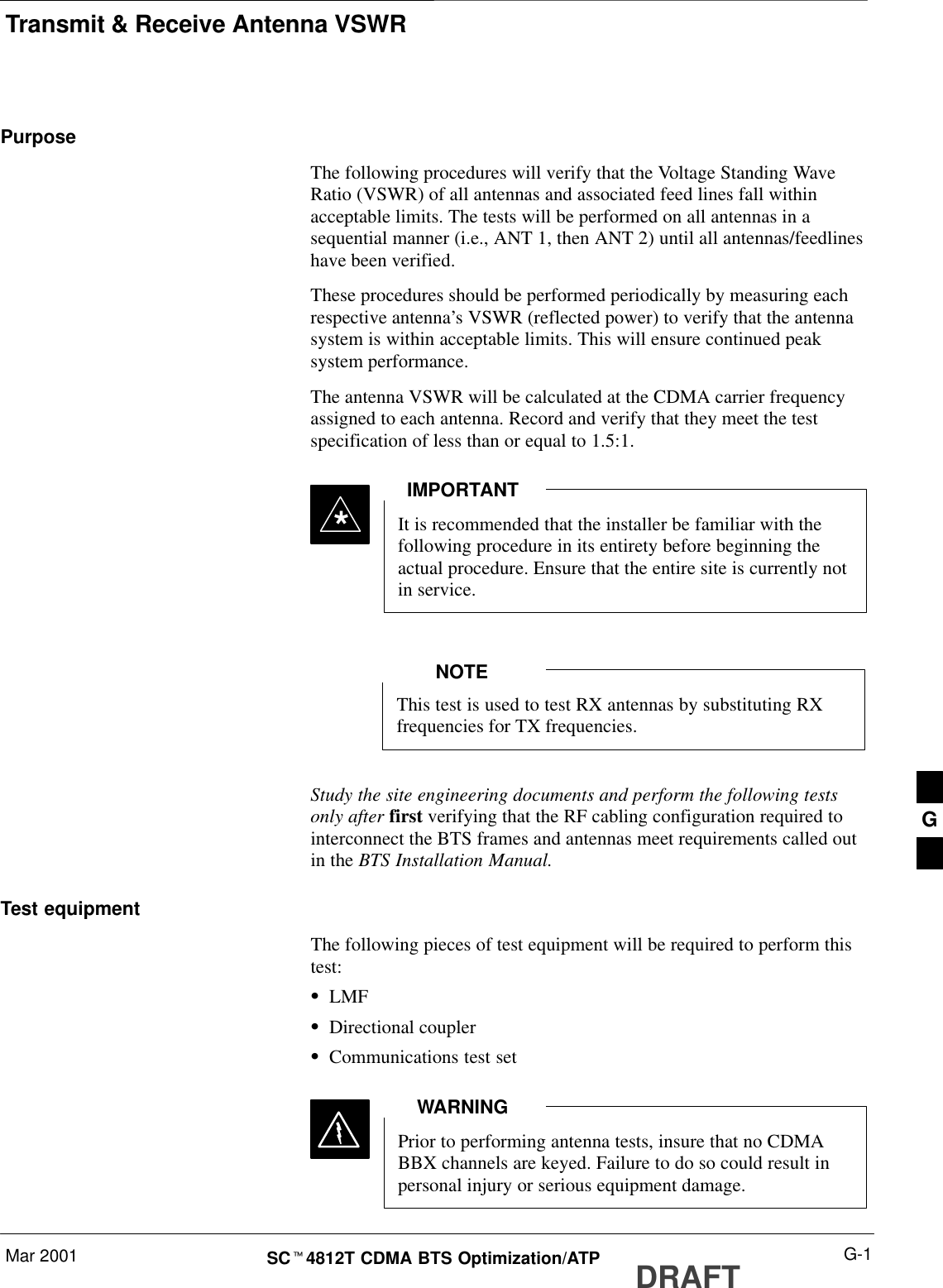
Nokia Solutions and Networks T5BL1 Part 22 CDMA Cellular Base Station User Manual IHET5BL1 Part 3 of 3

Nokia Solutions and Networks Part 22 CDMA Cellular Base Station IHET5BL1 Part 3 of 3

IHET5BL1 User Manual Part 3 of 3
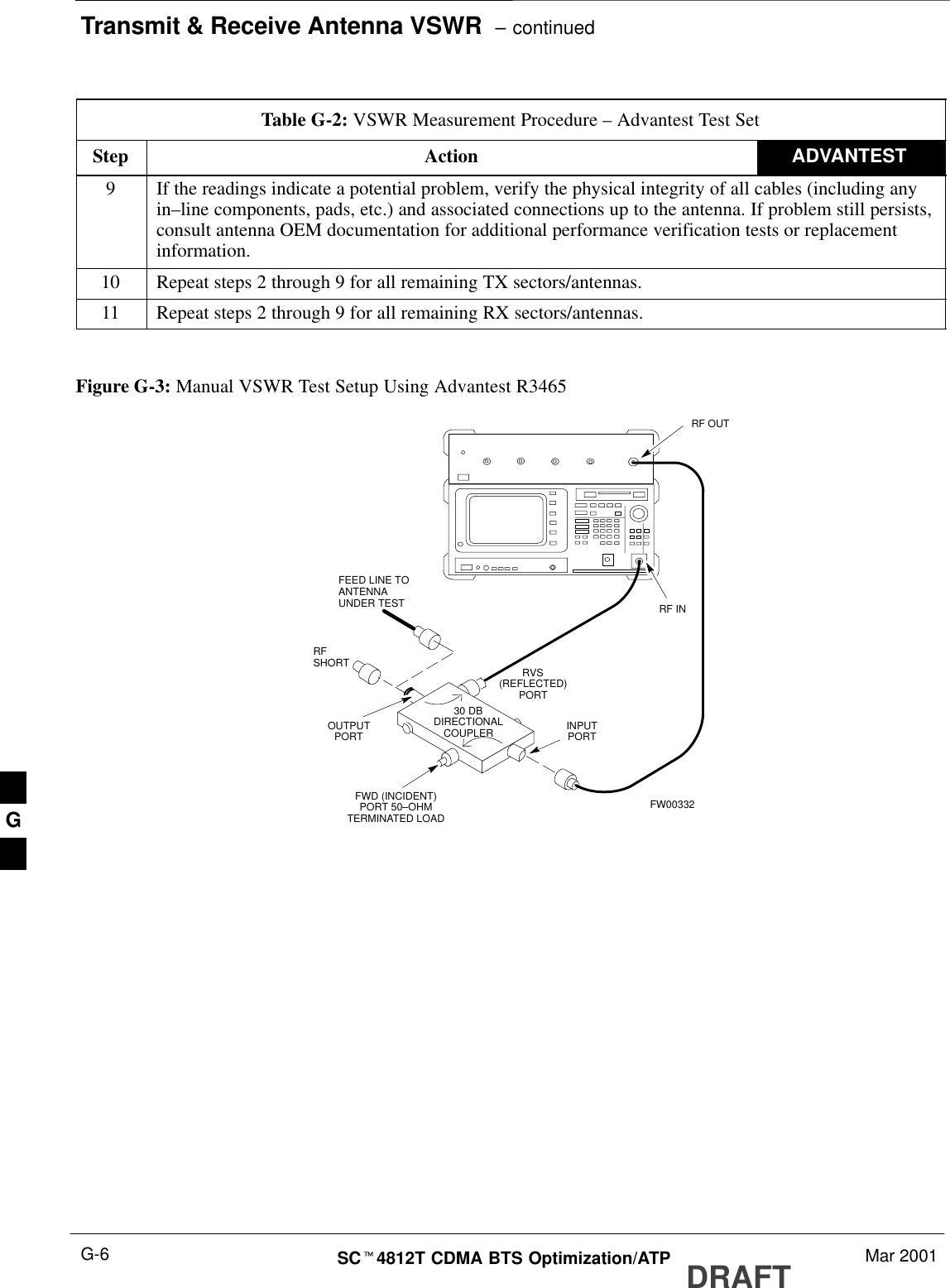
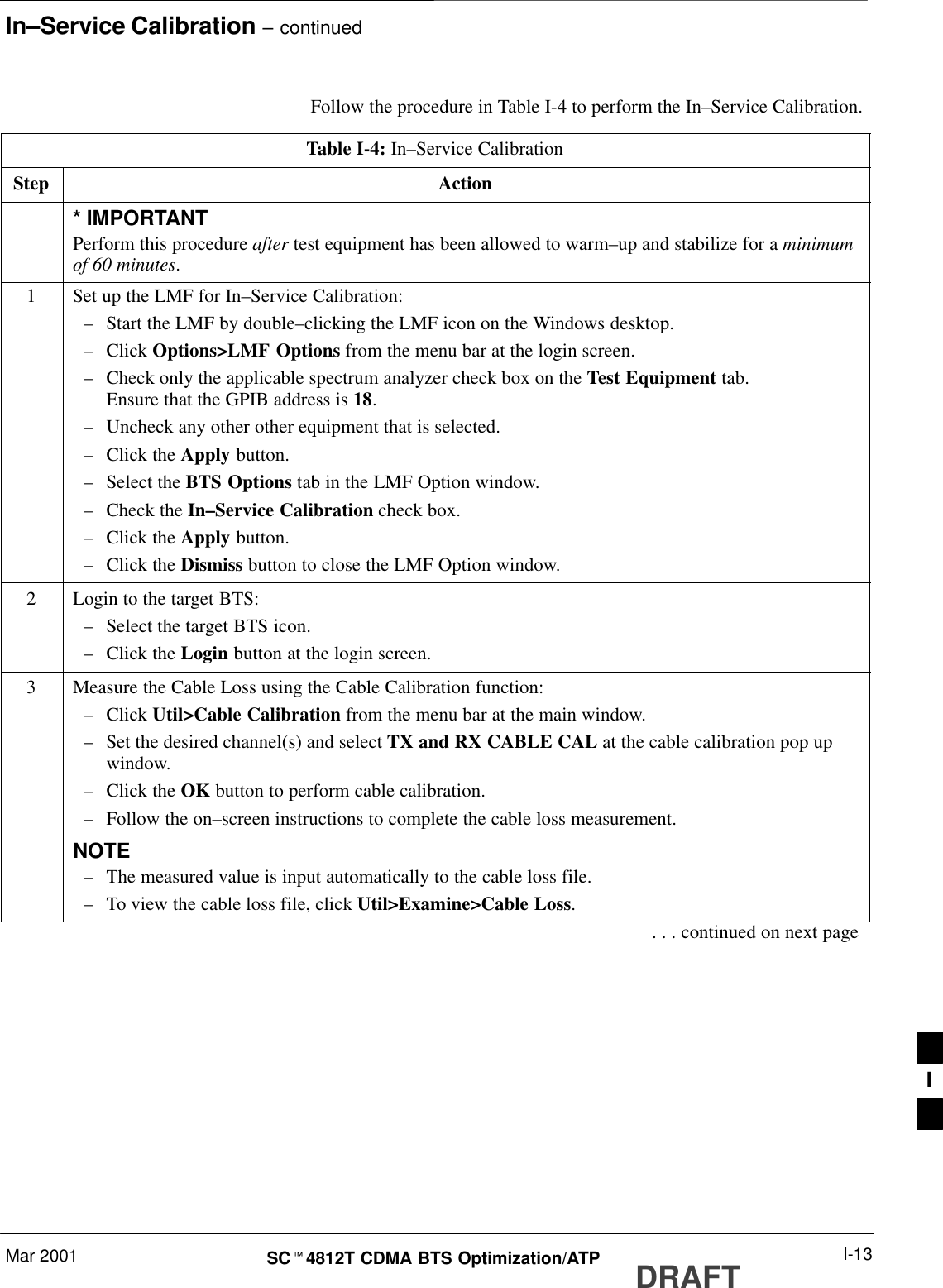
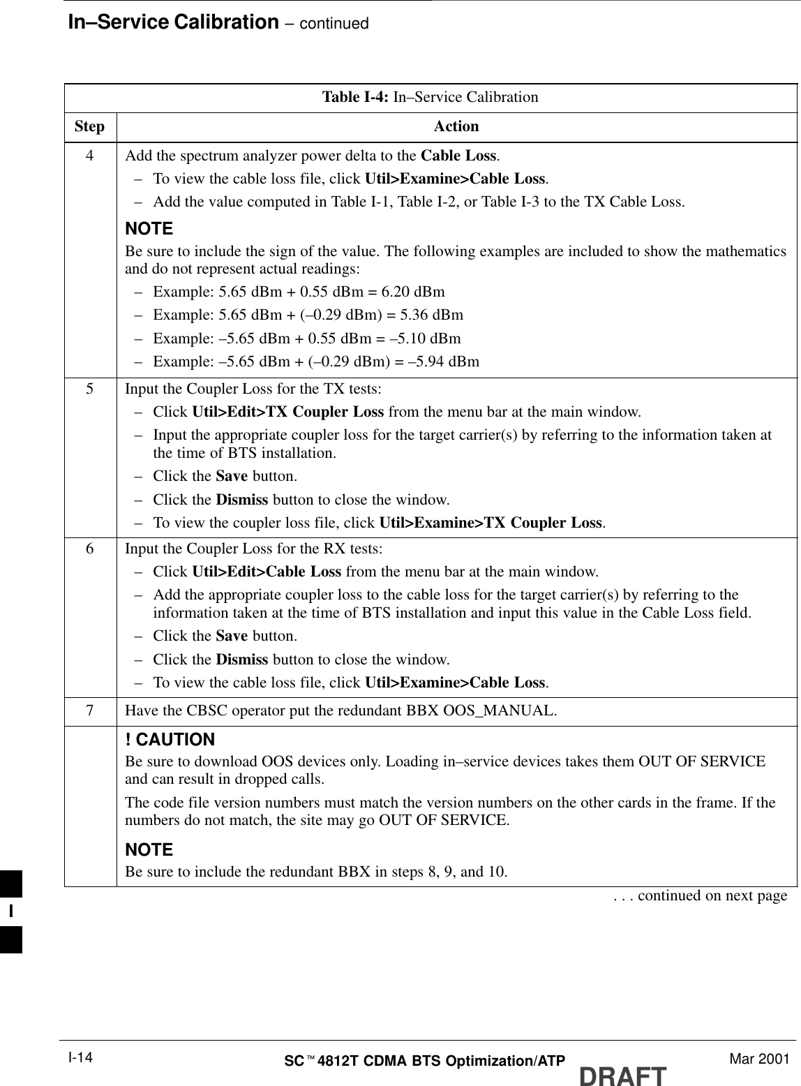
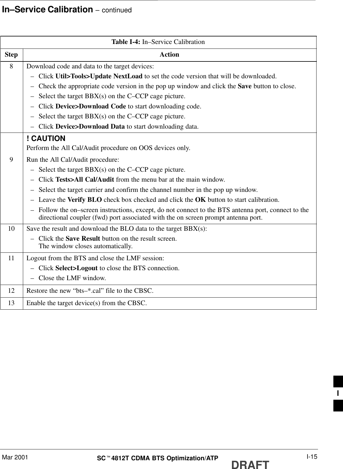
Automated Acceptance Test Procedures – All–inclusive TX & RXMar 2001 4-1SCt4812T CDMA BTS Optimization/ATP DRAFTIntroductionThe Automated Acceptance Test Procedure (ATP) allows Cellular FieldEngineers (CFEs) to run automated acceptance tests on all equipped BTSsubsystem devices using the Local Maintenance Facility (LMF) andsupported test equipment per the current Cell Site Data File (CDF)assignment.The results of these tests (at the option of the operator) are written to afile that can be printed. All tests are controlled from the LMF platformusing the GPIB interface, therefore, only recommended test equipmentsupported by the LMF can be used.This chapter describes the tests run from the GUI environment, which isthe recommended method. The GUI provides the advantages ofsimplifying the LMF user interface, reducing the potential for miskeyingcommmands and associated parameters, and speeding up the executionof complex operations involving multiple command strings. If you feelthe command line interface (CLI) will provide additional insight into theprogress of ATPs and problems that could possibly be encountered, referto LMF CLI Commands, R15.X (68P09251A59).Before performing any tests, use an editor to view the“CAVEATS” section of the “readme.txt” file in the c:\wlmffolder for any applicable information.The ATP test is to be performed on out-of-service (OOS)sectors only.DO NOT substitute test equipment not supported by theLMF.IMPORTANT*Refer to Chapter 3 for detailed information on test setconnections for calibrating equipment, cables and other testset components, if required.NOTECustomer requirements determine which ATP tests to are to beperformed, and the craftsperson selects the appropriate ATP tests to run.The tests can be run individually or as one of the following groups:SAll TX: TX tests verify the performance of the BTS transmit line up.These include the GLI, MCC, BBX, and CIO cards, the LPAs andpassive components including splitters, combiners, bandpass filters,and RF cables.SAll RX: RX tests verify the performance of the BTS receiver line up.These include the MPC (for starter frames), EMPC (for expansionframes), CIO, BBX, MCC, and GLI cards and the passive componentsincluding RX filters (starter frame only), and RF cables. . . . continued on next page4
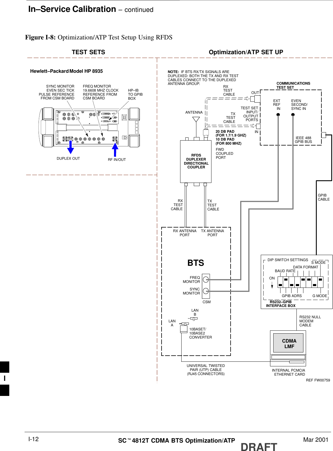
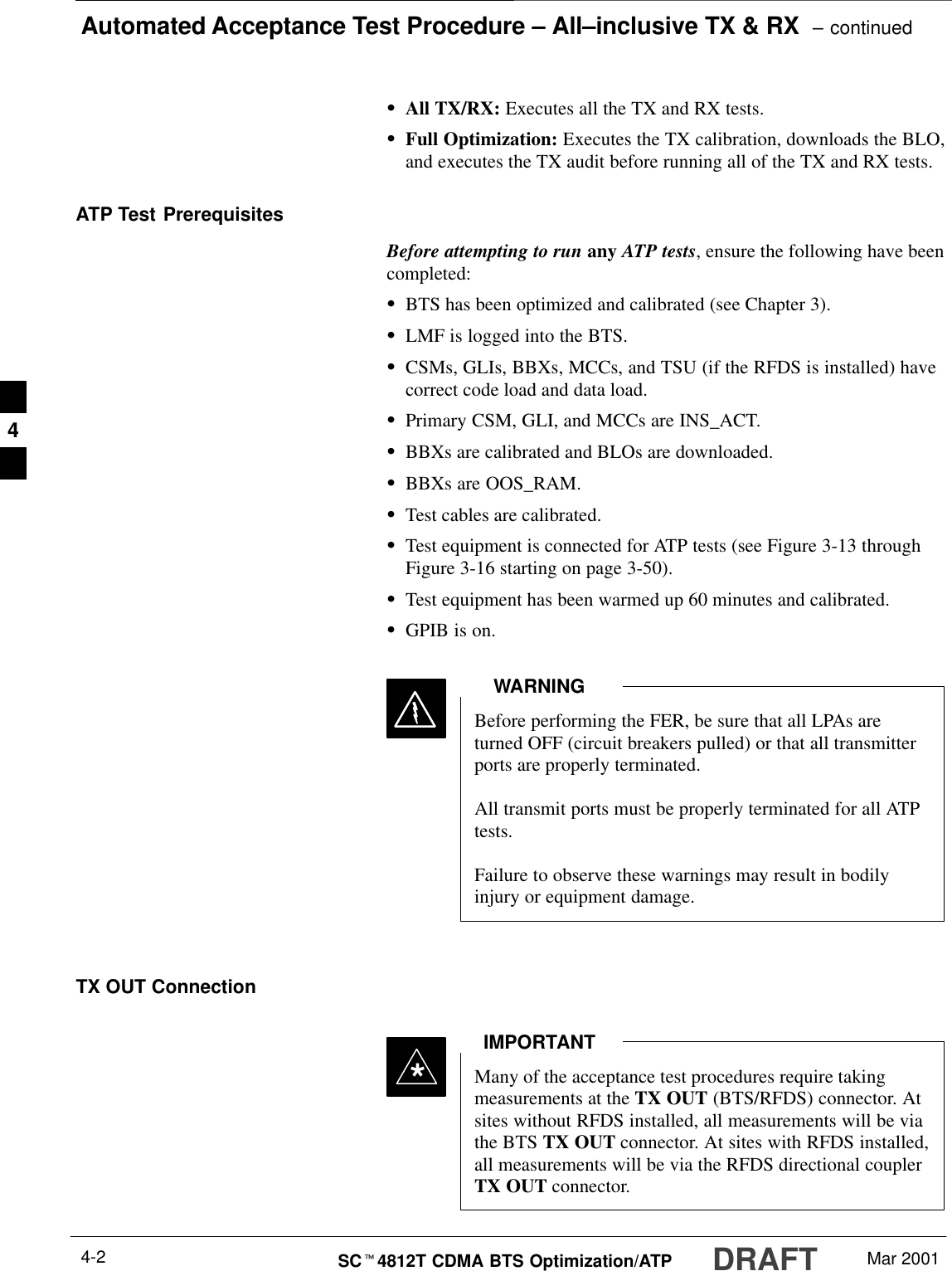
Automated Acceptance Test Procedure – All–inclusive TX & RX  – continuedDRAFTSCt4812T CDMA BTS Optimization/ATP Mar 20014-2SAll TX/RX: Executes all the TX and RX tests.SFull Optimization: Executes the TX calibration, downloads the BLO,and executes the TX audit before running all of the TX and RX tests.ATP Test PrerequisitesBefore attempting to run any ATP tests, ensure the following have beencompleted:SBTS has been optimized and calibrated (see Chapter 3).SLMF is logged into the BTS.SCSMs, GLIs, BBXs, MCCs, and TSU (if the RFDS is installed) havecorrect code load and data load.SPrimary CSM, GLI, and MCCs are INS_ACT.SBBXs are calibrated and BLOs are downloaded.SBBXs are OOS_RAM.STest cables are calibrated.STest equipment is connected for ATP tests (see Figure 3-13 throughFigure 3-16 starting on page 3-50).STest equipment has been warmed up 60 minutes and calibrated.SGPIB is on.Before performing the FER, be sure that all LPAs areturned OFF (circuit breakers pulled) or that all transmitterports are properly terminated.All transmit ports must be properly terminated for all ATPtests.Failure to observe these warnings may result in bodilyinjury or equipment damage.WARNINGTX OUT ConnectionMany of the acceptance test procedures require takingmeasurements at the TX OUT (BTS/RFDS) connector. Atsites without RFDS installed, all measurements will be viathe BTS TX OUT connector. At sites with RFDS installed,all measurements will be via the RFDS directional couplerTX OUT connector.IMPORTANT*4
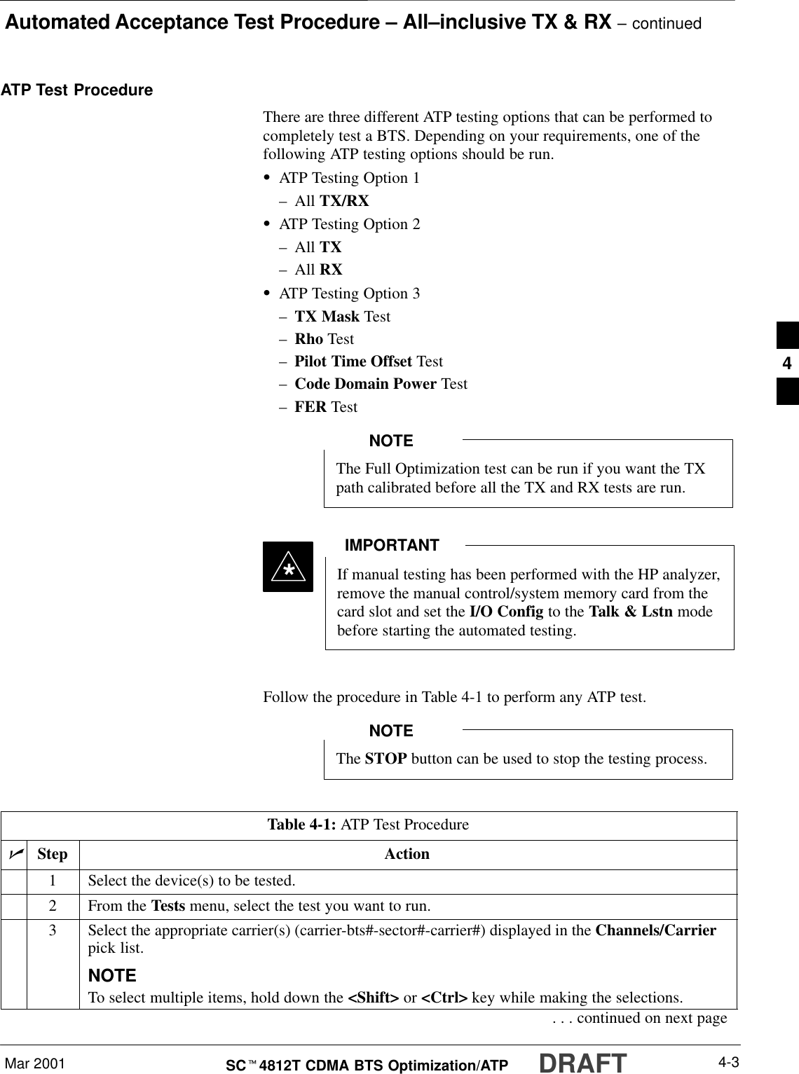
Automated Acceptance Test Procedure – All–inclusive TX & RX – continuedMar 2001 4-3SCt4812T CDMA BTS Optimization/ATP DRAFTATP Test ProcedureThere are three different ATP testing options that can be performed tocompletely test a BTS. Depending on your requirements, one of thefollowing ATP testing options should be run.SATP Testing Option 1–All TX/RXSATP Testing Option 2–All TX–All RXSATP Testing Option 3–TX Mask Test–Rho Test–Pilot Time Offset Test–Code Domain Power Test–FER TestThe Full Optimization test can be run if you want the TXpath calibrated before all the TX and RX tests are run.NOTEIf manual testing has been performed with the HP analyzer,remove the manual control/system memory card from thecard slot and set the I/O Config to the Talk & Lstn modebefore starting the automated testing.IMPORTANT*Follow the procedure in Table 4-1 to perform any ATP test.The STOP button can be used to stop the testing process.NOTETable 4-1: ATP Test ProcedurenStep Action1Select the device(s) to be tested.2From the Tests menu, select the test you want to run.3Select the appropriate carrier(s) (carrier-bts#-sector#-carrier#) displayed in the Channels/Carrierpick list.NOTETo select multiple items, hold down the <Shift> or <Ctrl> key while making the selections.. . . continued on next page4
Automated Acceptance Test Procedure – All–inclusive TX & RX  – continuedDRAFTSCt4812T CDMA BTS Optimization/ATP Mar 20014-4Table 4-1: ATP Test ProcedurenActionStep4Enter the appropriate channel number in the Carrier n Channels box.The default channel number displayed is determined by the CdmaChans[n] number in thecbsc–n.cdf file for the BTS.5Click on the OK button.The status report window and a Directions pop-up are displayed.6Follow the cable connection directions as they are displayed.The test results are displayed in the status report window.7Click on Save Results or Dismiss.NOTEIf Dismiss is used, the test results will not be saved in the test report file. 4
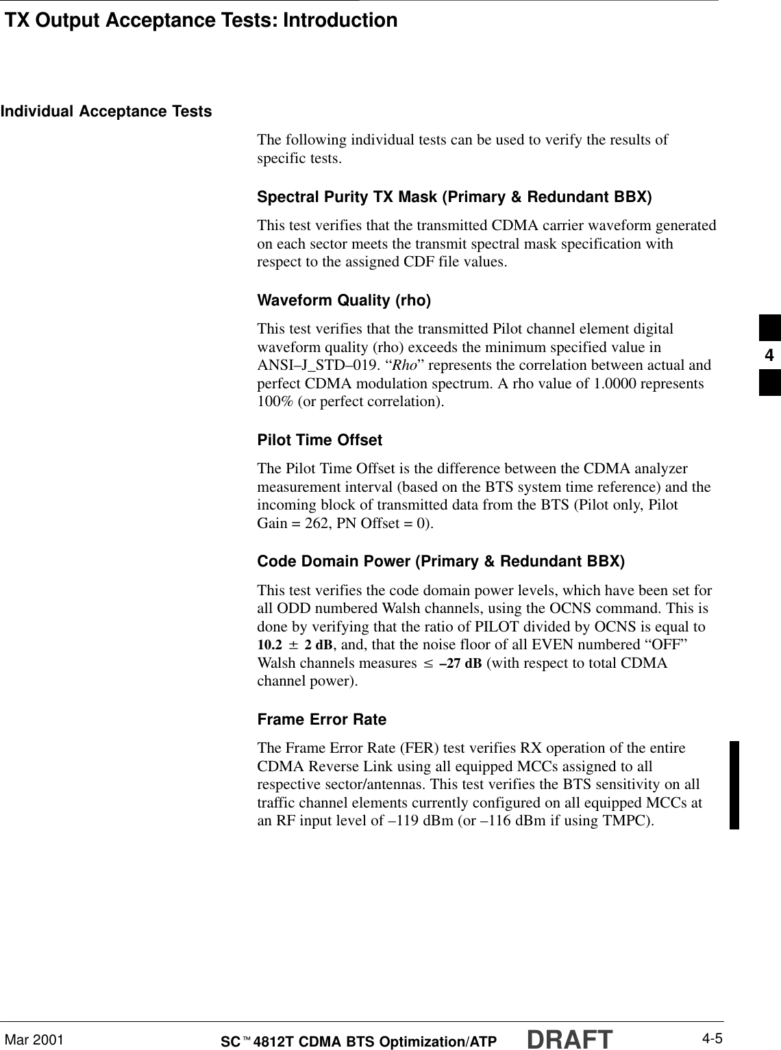
TX Output Acceptance Tests: IntroductionMar 2001 4-5SCt4812T CDMA BTS Optimization/ATP DRAFTIndividual Acceptance TestsThe following individual tests can be used to verify the results ofspecific tests.Spectral Purity TX Mask (Primary & Redundant BBX)This test verifies that the transmitted CDMA carrier waveform generatedon each sector meets the transmit spectral mask specification withrespect to the assigned CDF file values.Waveform Quality (rho)This test verifies that the transmitted Pilot channel element digitalwaveform quality (rho) exceeds the minimum specified value inANSI–J_STD–019. “Rho” represents the correlation between actual andperfect CDMA modulation spectrum. A rho value of 1.0000 represents100% (or perfect correlation).Pilot Time OffsetThe Pilot Time Offset is the difference between the CDMA analyzermeasurement interval (based on the BTS system time reference) and theincoming block of transmitted data from the BTS (Pilot only, PilotGain = 262, PN Offset = 0).Code Domain Power (Primary & Redundant BBX)This test verifies the code domain power levels, which have been set forall ODD numbered Walsh channels, using the OCNS command. This isdone by verifying that the ratio of PILOT divided by OCNS is equal to10.2 $ 2 dB, and, that the noise floor of all EVEN numbered “OFF”Walsh channels measures v –27 dB (with respect to total CDMAchannel power).Frame Error RateThe Frame Error Rate (FER) test verifies RX operation of the entireCDMA Reverse Link using all equipped MCCs assigned to allrespective sector/antennas. This test verifies the BTS sensitivity on alltraffic channel elements currently configured on all equipped MCCs atan RF input level of –119 dBm (or –116 dBm if using TMPC).4
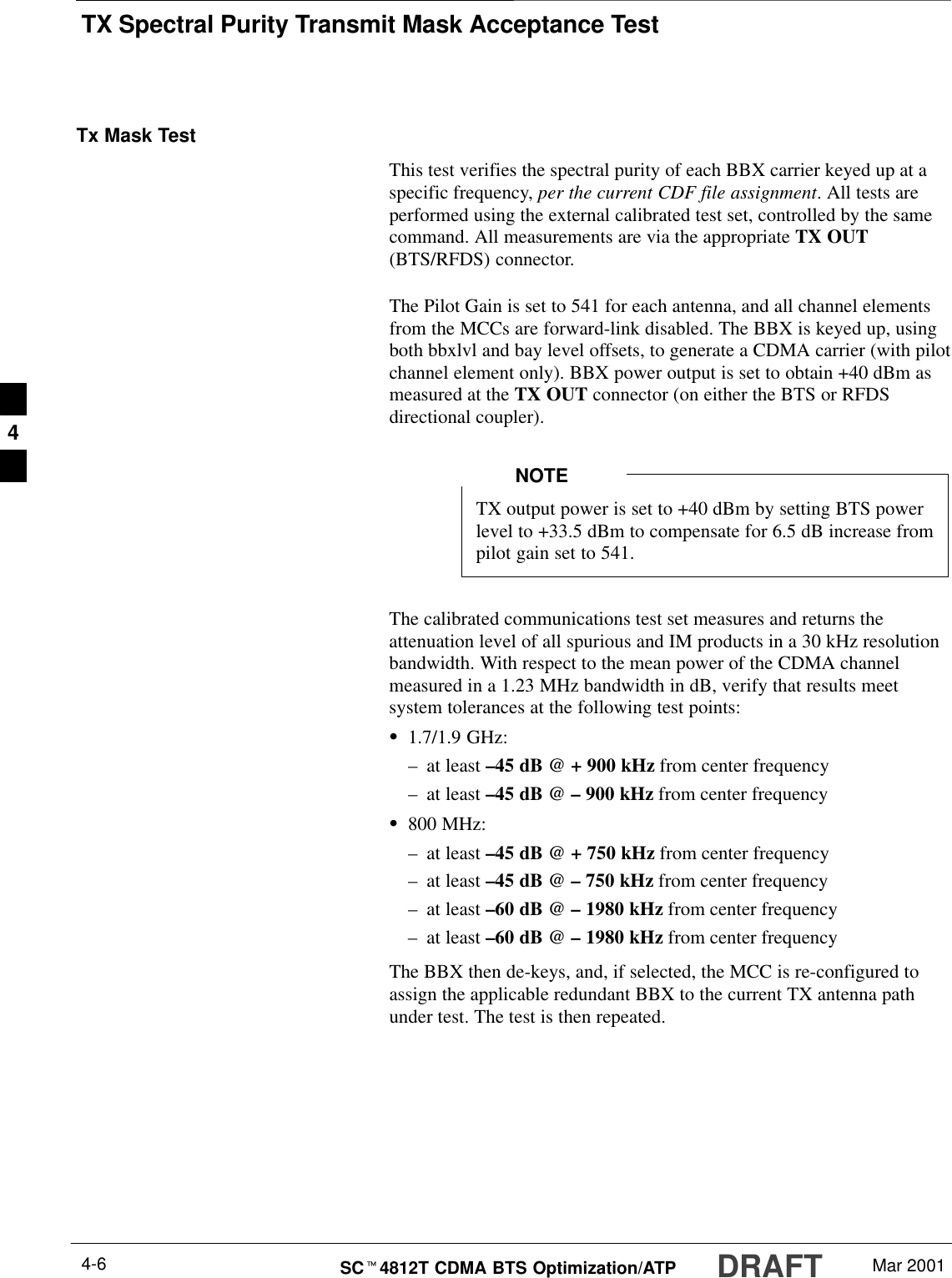
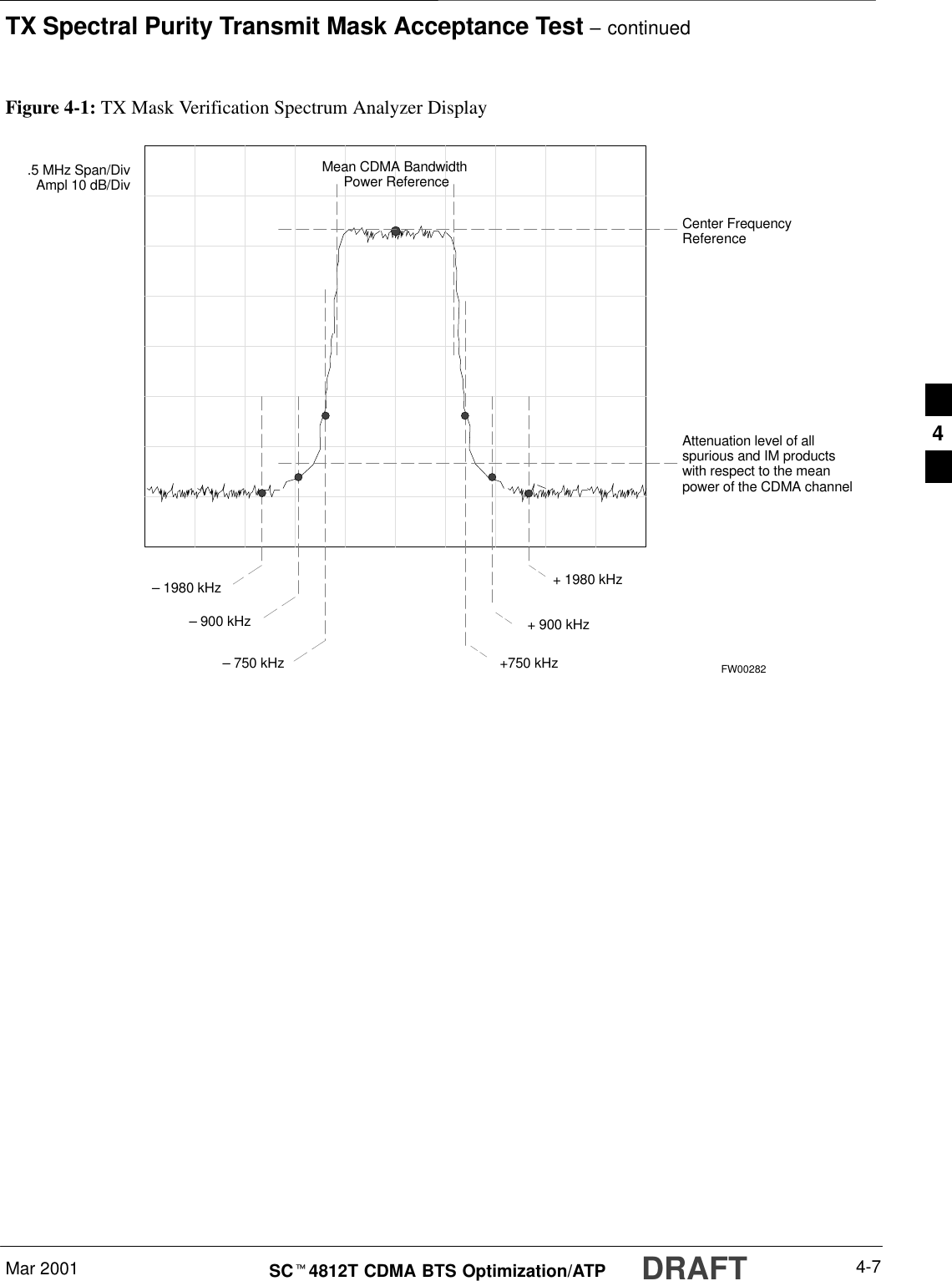
TX Spectral Purity Transmit Mask Acceptance TestDRAFTSCt4812T CDMA BTS Optimization/ATP Mar 20014-6Tx Mask TestThis test verifies the spectral purity of each BBX carrier keyed up at aspecific frequency, per the current CDF file assignment. All tests areperformed using the external calibrated test set, controlled by the samecommand. All measurements are via the appropriate TX OUT(BTS/RFDS) connector.The Pilot Gain is set to 541 for each antenna, and all channel elementsfrom the MCCs are forward-link disabled. The BBX is keyed up, usingboth bbxlvl and bay level offsets, to generate a CDMA carrier (with pilotchannel element only). BBX power output is set to obtain +40 dBm asmeasured at the TX OUT connector (on either the BTS or RFDSdirectional coupler).TX output power is set to +40 dBm by setting BTS powerlevel to +33.5 dBm to compensate for 6.5 dB increase frompilot gain set to 541.NOTEThe calibrated communications test set measures and returns theattenuation level of all spurious and IM products in a 30 kHz resolutionbandwidth. With respect to the mean power of the CDMA channelmeasured in a 1.23 MHz bandwidth in dB, verify that results meetsystem tolerances at the following test points:S1.7/1.9 GHz:–at least –45 dB @ + 900 kHz from center frequency–at least –45 dB @ – 900 kHz from center frequencyS800 MHz:–at least –45 dB @ + 750 kHz from center frequency–at least –45 dB @ – 750 kHz from center frequency–at least –60 dB @ – 1980 kHz from center frequency–at least –60 dB @ – 1980 kHz from center frequencyThe BBX then de-keys, and, if selected, the MCC is re-configured toassign the applicable redundant BBX to the current TX antenna pathunder test. The test is then repeated.4
TX Spectral Purity Transmit Mask Acceptance Test – continuedMar 2001 4-7SCt4812T CDMA BTS Optimization/ATP DRAFTFigure 4-1: TX Mask Verification Spectrum Analyzer Display– 900 kHz + 900 kHzCenter FrequencyReferenceAttenuation level of allspurious and IM productswith respect to the meanpower of the CDMA channel.5 MHz Span/DivAmpl 10 dB/DivMean CDMA Bandwidth Power Reference+750 kHz+ 1980 kHz– 750 kHz– 1980 kHzFW002824
TX Waveform Quality (rho) Acceptance TestDRAFTSCt4812T CDMA BTS Optimization/ATP Mar 20014-8Rho TestThis test verifies the transmitted Pilot channel element digital waveformquality of each BBX carrier keyed up at a specific frequency per thecurrent CDF file assignment. All tests are performed using the externalcalibrated test set controlled by the same command. All measurementsare via the appropriate TX OUT (BTS/RFDS) connector.The Pilot Gain is set to 262 for each antenna, and all channel elementsfrom the MCCs are forward link disabled. The BBX is keyed up usingboth bbxlvl and bay level offsets, to generate a CDMA carrier (with pilotchannel element only, Walsh code 0). BBX power output is set to40 dBm as measured at the TX OUT connector (on either the BTS orRFDS directional coupler).The calibrated communications test set measures and returns the Pilotchannel element digital waveform quality (rho) in dB, verifying that theresult meets system tolerances:SWaveform quality (rho) should be > 0.912 (–0.4 dB).The BBX then de-keys and, if selected, the MCC is re-configured toassign the applicable redundant BBX to the current TX antenna pathunder test. The test is then be repeated.4
TX Pilot Time Offset Acceptance TestMar 2001 4-9SCt4812T CDMA BTS Optimization/ATP DRAFTPilot Offset Acceptance TestThis test verifies the transmitted Pilot channel element Pilot Time Offsetof each BBX carrier keyed up at a specific frequency per the currentCDF file assignment. All tests are performed using the externalcalibrated test set controlled by the same command. All measurementsare via the appropriate TX OUT (BTS/RFDS) connector.The Pilot Gain is set to 262 for each antenna, and all TCH elements fromthe MCCs are forward link disabled. The BBX is keyed up, using bothbbxlvl and bay level offsets, to generate a CDMA carrier (with pilotchannel element only, Walsh code 0). BBX power output is set to40 dBm as measured at the TX OUT connector (on either the BTS orRFDS directional coupler).The calibrated communications test set measures and returns the PilotTime Offset in µs, verifying results meet system tolerances:SPilot Time Offset should be within < 3 µs of the target PTOffset (0 µs).The BBX then de-keys, and if selected, the MCC is re-configured toassign the applicable redundant BBX to the current TX antenna pathunder test. The test is then repeated.
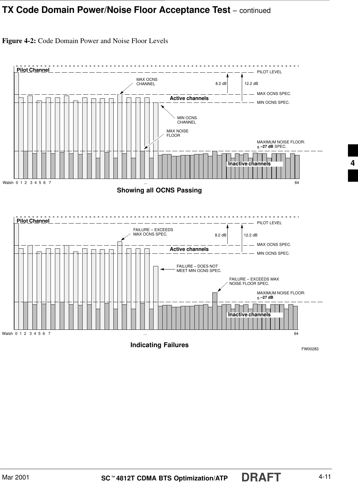
TX Code Domain Power/Noise Floor Acceptance TestDRAFTSCt4812T CDMA BTS Optimization/ATP Mar 20014-10Code Domain Power TestThis test verifies the Code Domain Power/Noise of each BBX carrierkeyed up at a specific frequency per the current CDF file assignment.All tests are performed using the external calibrated test set controlled bythe same command. All measurements are via the appropriate TX OUT(BTS/RFDS) connector.For each sector/antenna under test, the Pilot Gain is set to 262. All MCCchannel elements under test are configured to generate OrthogonalChannel Noise Source (OCNS) on different odd Walsh codes and to beassigned a full–rate gain of 81. The maximum number of MCC/CEs tobe tested an any one time is 32 (32 odd Walsh codes). If more than 32CEs exist, then multiple sets of measurements are made; so all channelelements are verified on all sectors.BBX power output is set to 40 dBm as measured at the TX OUTconnector (on either the BTS or RFDS directional coupler).You verify the code domain power levels, which have been set for allODD numbered Walsh channels, using the OCNS command. This isdone by verifying that Pilot Power (dBm) minus OCNS Power (dBm) isequal to 10.2 + 2 dB and that the noise floor of all “OFF” Walsh channelsmeasures  < –27 dB (with respect to total CDMA channel power).The BBX then de-keys and, if selected, the MCC is re-configured toassign the applicable redundant BBX to the current TX antenna pathunder test. The test is then repeated. Upon completion of the test, OCNSis disabled on the specified MCC/CE.4
TX Code Domain Power/Noise Floor Acceptance Test – continuedMar 2001 4-11SCt4812T CDMA BTS Optimization/ATP DRAFTFigure 4-2: Code Domain Power and Noise Floor LevelsPilot ChannelActive channelsPILOT LEVELMAX OCNS SPEC.MIN OCNS SPEC.MAXIMUM NOISE FLOOR: < –27 dB SPEC.Inactive channelsWalsh  0  1  2   3  4  5  6   7  ... 64MAX OCNSCHANNELMIN OCNSCHANNEL8.2 dB 12.2 dBMAX NOISEFLOORPilot ChannelActive channelsPILOT LEVELMAX OCNS SPEC.MIN OCNS SPEC.MAXIMUM NOISE FLOOR:< –27 dBInactive channelsWalsh  0  1  2   3  4  5  6   7  ... 64FAILURE – DOES NOTMEET MIN OCNS SPEC.FAILURE – EXCEEDSMAX OCNS SPEC. 8.2 dB 12.2 dBFAILURE – EXCEEDS MAXNOISE FLOOR SPEC. Showing all OCNS Passing Indicating Failures FW002834
RX Frame Error Rate (FER) Acceptance TestDRAFTSCt4812T CDMA BTS Optimization/ATP Mar 20014-12FER TestThis test verifies the BTS FER on all traffic channel elements currentlyconfigured on all equipped MCCs (full rate at 1% FER) at an RF inputlevel of –119 dBm [or –116 dBm if using Tower TopAmplifier (TMPC)]. All tests are performed using the external calibratedtest set as the signal source controlled by the same command. Allmeasurements are via the LMF.The Pilot Gain is set to 262 for each TX antenna, and all channelelements from the MCCs are forward-link disabled. The BBX is keyedup, using only bbxlvl level offsets, to generate a CDMA carrier (withpilot channel element only). BBX power output is set to –20 dBm asmeasured at the TX OUT connector (on either the BTS or RFDSdirectional coupler). The BBX must be keyed to enable the RX receivecircuitry.The LMF prompts the MCC/CE under test to measure all zero longcodeand provide the FER report on the selected active MCC on the reverselink for both the main and diversity RX antenna paths, verifying thatresults meet the following specification:SFER returned less than 1% and total frames measured is 1500All MCC/CEs selected are tested on the specified RX antenna path. TheBBX then de-keys and, if selected, the MCC is re-configured to assignthe applicable redundant BBX to the current RX antenna paths undertest. The test is then repeated.4
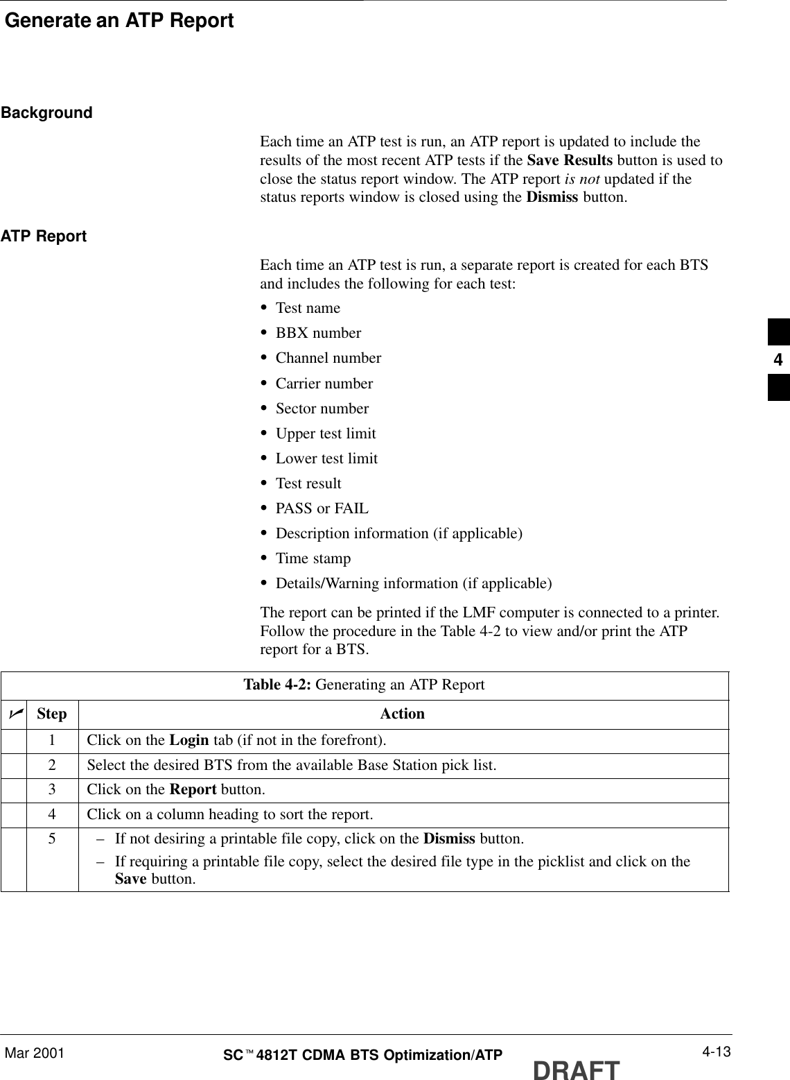
Generate an ATP ReportMar 2001 4-13SCt4812T CDMA BTS Optimization/ATP DRAFTBackgroundEach time an ATP test is run, an ATP report is updated to include theresults of the most recent ATP tests if the Save Results button is used toclose the status report window. The ATP report is not updated if thestatus reports window is closed using the Dismiss button.ATP ReportEach time an ATP test is run, a separate report is created for each BTSand includes the following for each test:STest nameSBBX numberSChannel numberSCarrier numberSSector numberSUpper test limitSLower test limitSTest resultSPASS or FAILSDescription information (if applicable)STime stampSDetails/Warning information (if applicable)The report can be printed if the LMF computer is connected to a printer.Follow the procedure in the Table 4-2 to view and/or print the ATPreport for a BTS.Table 4-2: Generating an ATP ReportnStep Action1Click on the Login tab (if not in the forefront).2Select the desired BTS from the available Base Station pick list.3Click on the Report button.4Click on a column heading to sort the report.5–If not desiring a printable file copy, click on the Dismiss button.–If requiring a printable file copy, select the desired file type in the picklist and click on theSave button.4
Generate an ATP Report – continuedDRAFTSCt4812T CDMA BTS Optimization/ATP Mar 20014-14Notes4
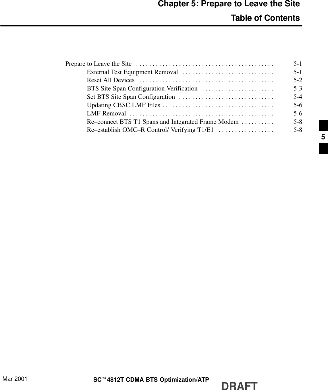
Mar 2001 SCt4812T CDMA BTS Optimization/ATP DRAFTChapter 5: Prepare to Leave the SiteTable of ContentsPrepare to Leave the Site 5-1. . . . . . . . . . . . . . . . . . . . . . . . . . . . . . . . . . . . . . . . . . External Test Equipment Removal 5-1. . . . . . . . . . . . . . . . . . . . . . . . . . . . Reset All Devices 5-2. . . . . . . . . . . . . . . . . . . . . . . . . . . . . . . . . . . . . . . . . BTS Site Span Configuration Verification 5-3. . . . . . . . . . . . . . . . . . . . . . Set BTS Site Span Configuration 5-4. . . . . . . . . . . . . . . . . . . . . . . . . . . . . Updating CBSC LMF Files 5-6. . . . . . . . . . . . . . . . . . . . . . . . . . . . . . . . . . LMF Removal 5-6. . . . . . . . . . . . . . . . . . . . . . . . . . . . . . . . . . . . . . . . . . . . Re–connect BTS T1 Spans and Integrated Frame Modem 5-8. . . . . . . . . . Re–establish OMC–R Control/ Verifying T1/E1 5-8. . . . . . . . . . . . . . . . .  5
Table of Contents  – continuedDRAFTSCt4812T CDMA BTS Optimization/ATP Mar 2001Notes5
Prepare to Leave the SiteMar 2001 5-1SCt4812T CDMA BTS Optimization/ATP DRAFTExternal Test EquipmentRemovalPerform the procedure in Table 5-1 to disconnect the test equipment andconfigure the BTS for active service.Table 5-1: External Test Equipment RemovalStep Action1Disconnect all external test equipment from all TX and RX connectors on the top of the frame.2Reconnect and visually inspect all TX and RX antenna feed lines at the top of the frame.Verify that all sector antenna feed lines are connected to thecorrect ports on the frame. Crossed antenna cables willcause system degradation of call processing.CAUTIONEach module or device can be in any state prior todownloading. Each module or device will be in anOOS_RAM state after downloading has completed.–For all LMF commands, information in italicsrepresents valid ranges for that command field.–Only those fields requiring an input will be specified.Default values for other fields will be assumed.–For more complete command examples (includingsystem response details), refer to the CDMA LMFUser  Guide.NOTE5
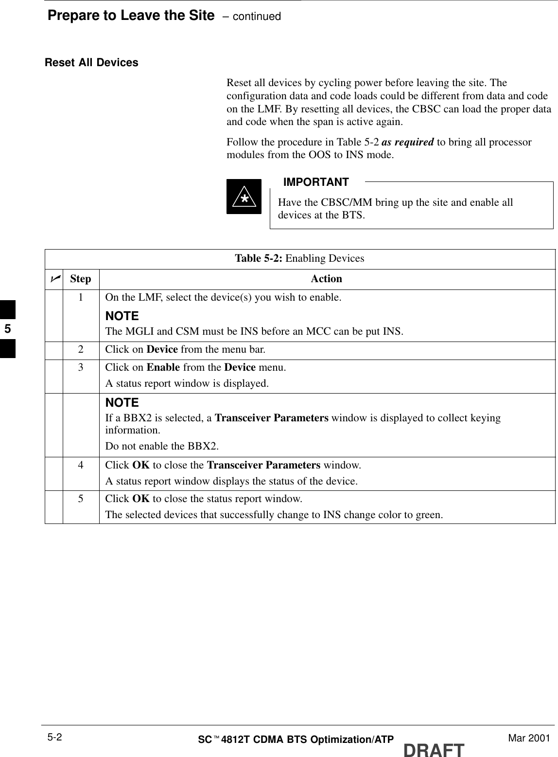
Prepare to Leave the Site  – continuedDRAFTSCt4812T CDMA BTS Optimization/ATP Mar 20015-2Reset All DevicesReset all devices by cycling power before leaving the site. Theconfiguration data and code loads could be different from data and codeon the LMF. By resetting all devices, the CBSC can load the proper dataand code when the span is active again.Follow the procedure in Table 5-2 as required to bring all processormodules from the OOS to INS mode.Have the CBSC/MM bring up the site and enable alldevices at the BTS.IMPORTANT*Table 5-2: Enabling DevicesnStep Action1On the LMF, select the device(s) you wish to enable.NOTEThe MGLI and CSM must be INS before an MCC can be put INS.2Click on Device from the menu bar.3Click on Enable from the Device menu.A status report window is displayed.NOTEIf a BBX2 is selected, a Transceiver Parameters window is displayed to collect keyinginformation.Do not enable the BBX2.4 Click OK to close the Transceiver Parameters window.A status report window displays the status of the device.5 Click OK to close the status report window.The selected devices that successfully change to INS change color to green.5
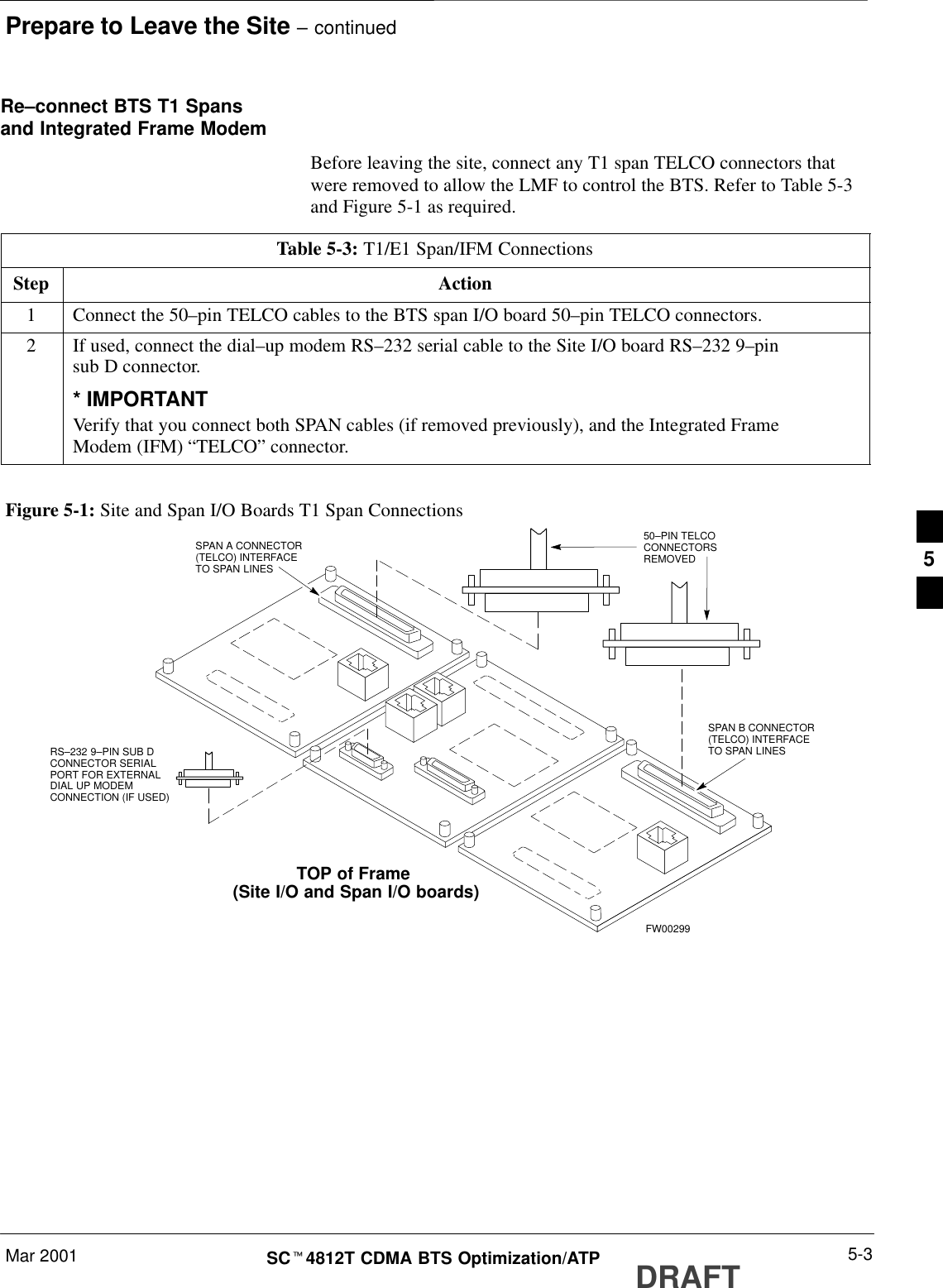
Prepare to Leave the Site – continuedMar 2001 5-3SCt4812T CDMA BTS Optimization/ATP DRAFTRe–connect BTS T1 Spansand Integrated Frame ModemBefore leaving the site, connect any T1 span TELCO connectors thatwere removed to allow the LMF to control the BTS. Refer to Table 5-3and Figure 5-1 as required.Table 5-3: T1/E1 Span/IFM ConnectionsStep Action1Connect the 50–pin TELCO cables to the BTS span I/O board 50–pin TELCO connectors.2If used, connect the dial–up modem RS–232 serial cable to the Site I/O board RS–232 9–pinsub D connector.* IMPORTANTVerify that you connect both SPAN cables (if removed previously), and the Integrated FrameModem (IFM) “TELCO” connector.Figure 5-1: Site and Span I/O Boards T1 Span Connections50–PIN TELCOCONNECTORSREMOVEDSPAN A CONNECTOR(TELCO) INTERFACETO SPAN LINESSPAN B CONNECTOR(TELCO) INTERFACETO SPAN LINESTOP of Frame (Site I/O and Span I/O boards)RS–232 9–PIN SUB DCONNECTOR SERIALPORT FOR EXTERNALDIAL UP MODEMCONNECTION (IF USED)FW002995
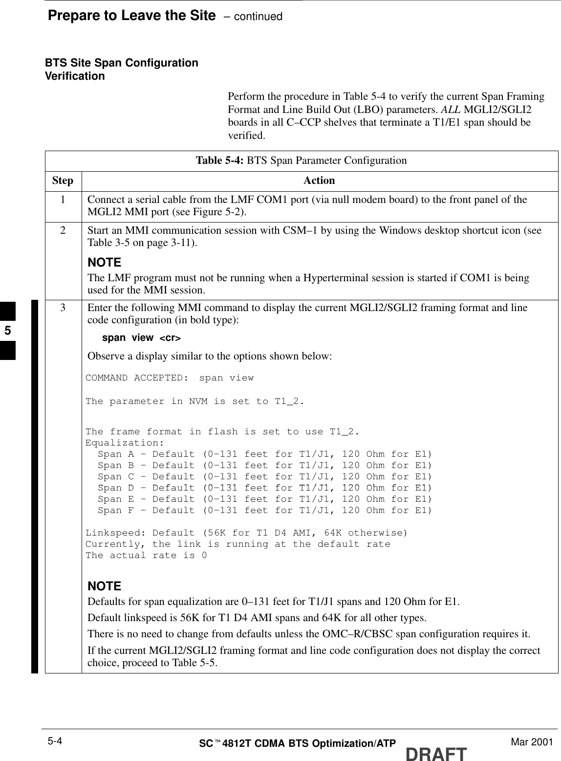
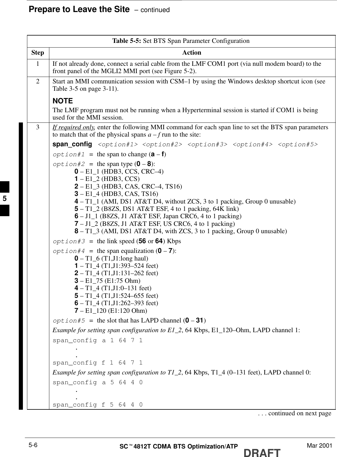
Prepare to Leave the Site  – continuedDRAFTSCt4812T CDMA BTS Optimization/ATP Mar 20015-4BTS Site Span ConfigurationVerificationPerform the procedure in Table 5-4 to verify the current Span FramingFormat and Line Build Out (LBO) parameters. ALL MGLI2/SGLI2boards in all C–CCP shelves that terminate a T1/E1 span should beverified.Table 5-4: BTS Span Parameter ConfigurationStep Action1Connect a serial cable from the LMF COM1 port (via null modem board) to the front panel of theMGLI2 MMI port (see Figure 5-2).2Start an MMI communication session with CSM–1 by using the Windows desktop shortcut icon (seeTable 3-5 on page 3-11).NOTEThe LMF program must not be running when a Hyperterminal session is started if COM1 is beingused for the MMI session.3Enter the following MMI command to display the current MGLI2/SGLI2 framing format and linecode configuration (in bold type):span view <cr>Observe a display similar to the options shown below:COMMAND ACCEPTED: span viewThe parameter in NVM is set to T1_2.The frame format in flash is set to use T1_2.Equalization:  Span A – Default (0–131 feet for T1/J1, 120 Ohm for E1)  Span B – Default (0–131 feet for T1/J1, 120 Ohm for E1)  Span C – Default (0–131 feet for T1/J1, 120 Ohm for E1)SDD f lt (0 131 f t f T1/J1 120 Oh f E1)  Span D – Default (0–131 feet for T1/J1, 120 Ohm for E1)  Span E – Default (0–131 feet for T1/J1, 120 Ohm for E1)  Span F – Default (0–131 feet for T1/J1, 120 Ohm for E1)Linkspeed: Default (56K for T1 D4 AMI, 64K otherwise)Currently, the link is running at the default rate The actual rate is 0NOTEDefaults for span equalization are 0–131 feet for T1/J1 spans and 120 Ohm for E1.Default linkspeed is 56K for T1 D4 AMI spans and 64K for all other types.There is no need to change from defaults unless the OMC–R/CBSC span configuration requires it.If the current MGLI2/SGLI2 framing format and line code configuration does not display the correctchoice, proceed to Table 5-5.5
Prepare to Leave the Site – continuedMar 2001 5-5SCt4812T CDMA BTS Optimization/ATP DRAFTTable 5-4: BTS Span Parameter ConfigurationStep Action4Repeat steps 1 through 3 for all remaining GLIs.5Exit the GLI MMI session and HyperTerminal connection by selecting File from the connectionwindow menu bar, and then Exit from the dropdown menu.FW003449–PIN TO 9– PINRS–232 CABLENULL MODEM BOARD(PART# 8484877P01)RS–232 CABLE FROM LMF COM1PORTMMI SERIAL PORTGLI BOARDFigure 5-2: MGLI2/SGLI2 MMI Port ConnectionSet BTS Site SpanConfigurationPerform the procedure in Table 5-5 to configure the Span FramingFormat and Line Build Out (LBO) parameters. ALL MGLI2/SGLI2boards in all C–CCP shelves that terminate a T1/E1 span must beconfigured.Perform the following procedure ONLY if spanconfigurations loaded in the MGLI2/GLI2s do not matchthose in the OMCR/CBSC data base, AND ONLY when theexact configuration data is available. Loading incorrectspan configuration data will render the site inoperable.IMPORTANT*5
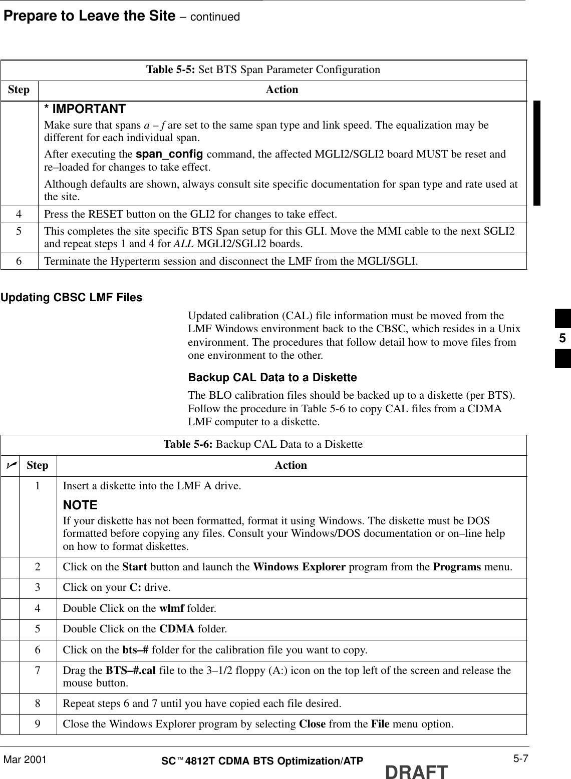
Prepare to Leave the Site  – continuedDRAFTSCt4812T CDMA BTS Optimization/ATP Mar 20015-6Table 5-5: Set BTS Span Parameter ConfigurationStep Action1If not already done, connect a serial cable from the LMF COM1 port (via null modem board) to thefront panel of the MGLI2 MMI port (see Figure 5-2).2Start an MMI communication session with CSM–1 by using the Windows desktop shortcut icon (seeTable 3-5 on page 3-11).NOTEThe LMF program must not be running when a Hyperterminal session is started if COM1 is beingused for the MMI session.3If required only, enter the following MMI command for each span line to set the BTS span parametersto match that of the physical spans a – f run to the site:span_config <option#1> <option#2> <option#3> <option#4> <option#5>option#1  =  the span to change (a – f)option#2  =  the span type (0 – 8):0 – E1_1 (HDB3, CCS, CRC–4)1 – E1_2 (HDB3, CCS)2 – E1_3 (HDB3, CAS, CRC–4, TS16)3 – E1_4 (HDB3, CAS, TS16)4 – T1_1 (AMI, DS1 AT&T D4, without ZCS, 3 to 1 packing, Group 0 unusable)5 – T1_2 (B8ZS, DS1 AT&T ESF, 4 to 1 packing, 64K link)6 – J1_1 (B8ZS, J1 AT&T ESF, Japan CRC6, 4 to 1 packing)7 – J1_2 (B8ZS, J1 AT&T ESF, US CRC6, 4 to 1 packing)8 – T1_3 (AMI, DS1 AT&T D4, with ZCS, 3 to 1 packing, Group 0 unusable)option#3  =  the link speed (56 or 64) Kbpsoption#4  =  the span equalization (0 – 7):0 – T1_6 (T1,J1:long haul)1 – T1_4 (T1,J1:393–524 feet)2 – T1_4 (T1,J1:131–262 feet)3 – E1_75 (E1:75 Ohm)4 – T1_4 (T1,J1:0–131 feet)5 – T1_4 (T1,J1:524–655 feet)6 – T1_4 (T1,J1:262–393 feet)7 – E1_120 (E1:120 Ohm)option#5  =  the slot that has LAPD channel (0 – 31)Example for setting span configuration to E1_2, 64 Kbps, E1_120–Ohm, LAPD channel 1:span_config a 1 64 7 1..span_config f 1 64 7 1Example for setting span configuration to T1_2, 64 Kbps, T1_4 (0–131 feet), LAPD channel 0:span_config a 5 64 4 0..span_config f 5 64 4 0. . . continued on next page5
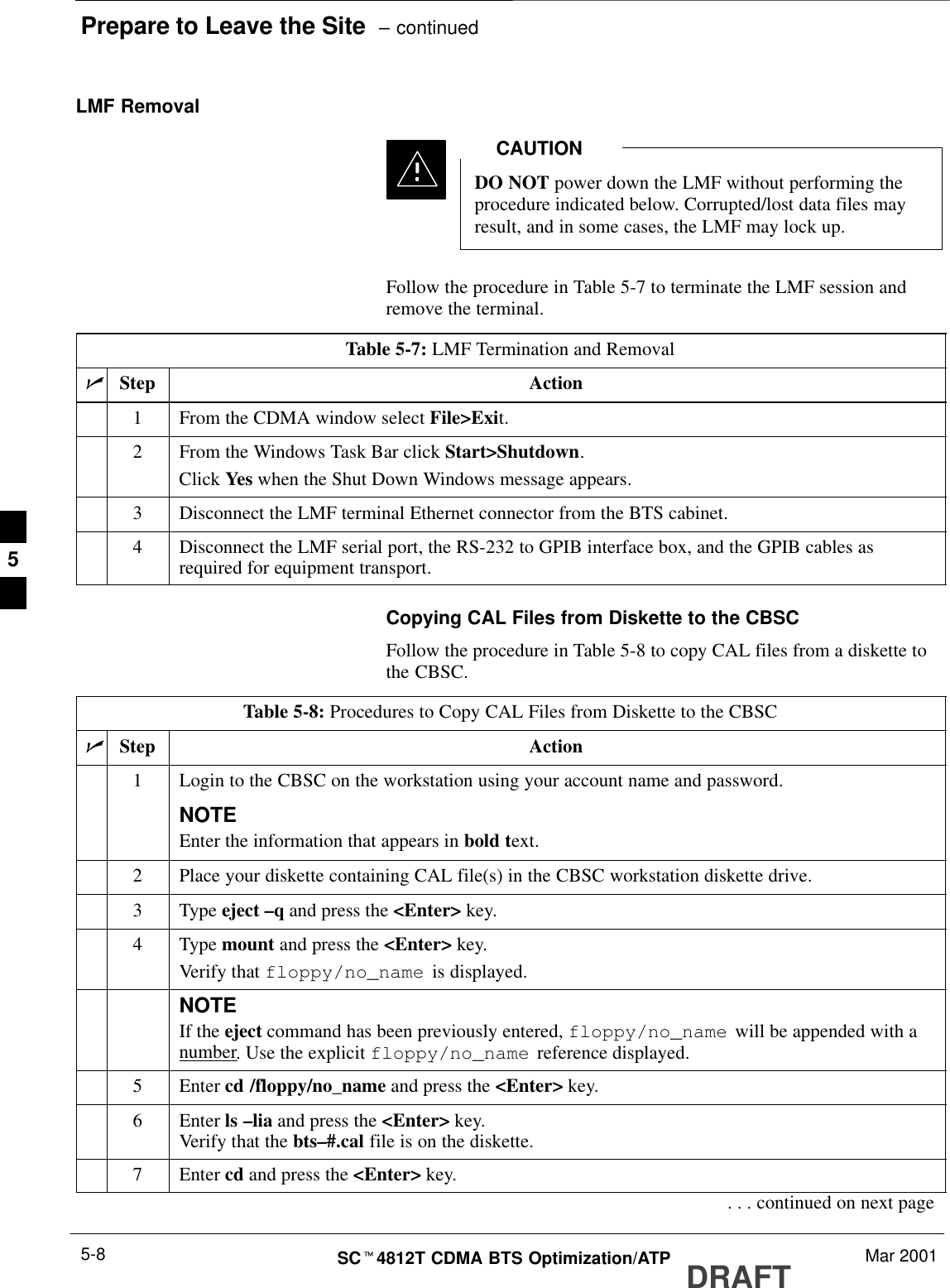
Prepare to Leave the Site – continuedMar 2001 5-7SCt4812T CDMA BTS Optimization/ATP DRAFTTable 5-5: Set BTS Span Parameter ConfigurationStep Action* IMPORTANTMake sure that spans a – f are set to the same span type and link speed. The equalization may bedifferent for each individual span.After executing the span_config command, the affected MGLI2/SGLI2 board MUST be reset andre–loaded for changes to take effect.Although defaults are shown, always consult site specific documentation for span type and rate used atthe site.4Press the RESET button on the GLI2 for changes to take effect.5This completes the site specific BTS Span setup for this GLI. Move the MMI cable to the next SGLI2and repeat steps 1 and 4 for ALL MGLI2/SGLI2 boards.6Terminate the Hyperterm session and disconnect the LMF from the MGLI/SGLI. Updating CBSC LMF FilesUpdated calibration (CAL) file information must be moved from theLMF Windows environment back to the CBSC, which resides in a Unixenvironment. The procedures that follow detail how to move files fromone environment to the other.Backup CAL Data to a DisketteThe BLO calibration files should be backed up to a diskette (per BTS).Follow the procedure in Table 5-6 to copy CAL files from a CDMALMF computer to a diskette.Table 5-6: Backup CAL Data to a DiskettenStep Action1Insert a diskette into the LMF A drive.NOTEIf your diskette has not been formatted, format it using Windows. The diskette must be DOSformatted before copying any files. Consult your Windows/DOS documentation or on–line helpon how to format diskettes.2Click on the Start button and launch the Windows Explorer program from the Programs menu.3Click on your C: drive.4Double Click on the wlmf folder.5Double Click on the CDMA folder.6Click on the bts–# folder for the calibration file you want to copy.7Drag the BTS–#.cal file to the 3–1/2 floppy (A:) icon on the top left of the screen and release themouse button.8Repeat steps 6 and 7 until you have copied each file desired.9Close the Windows Explorer program by selecting Close from the File menu option.5
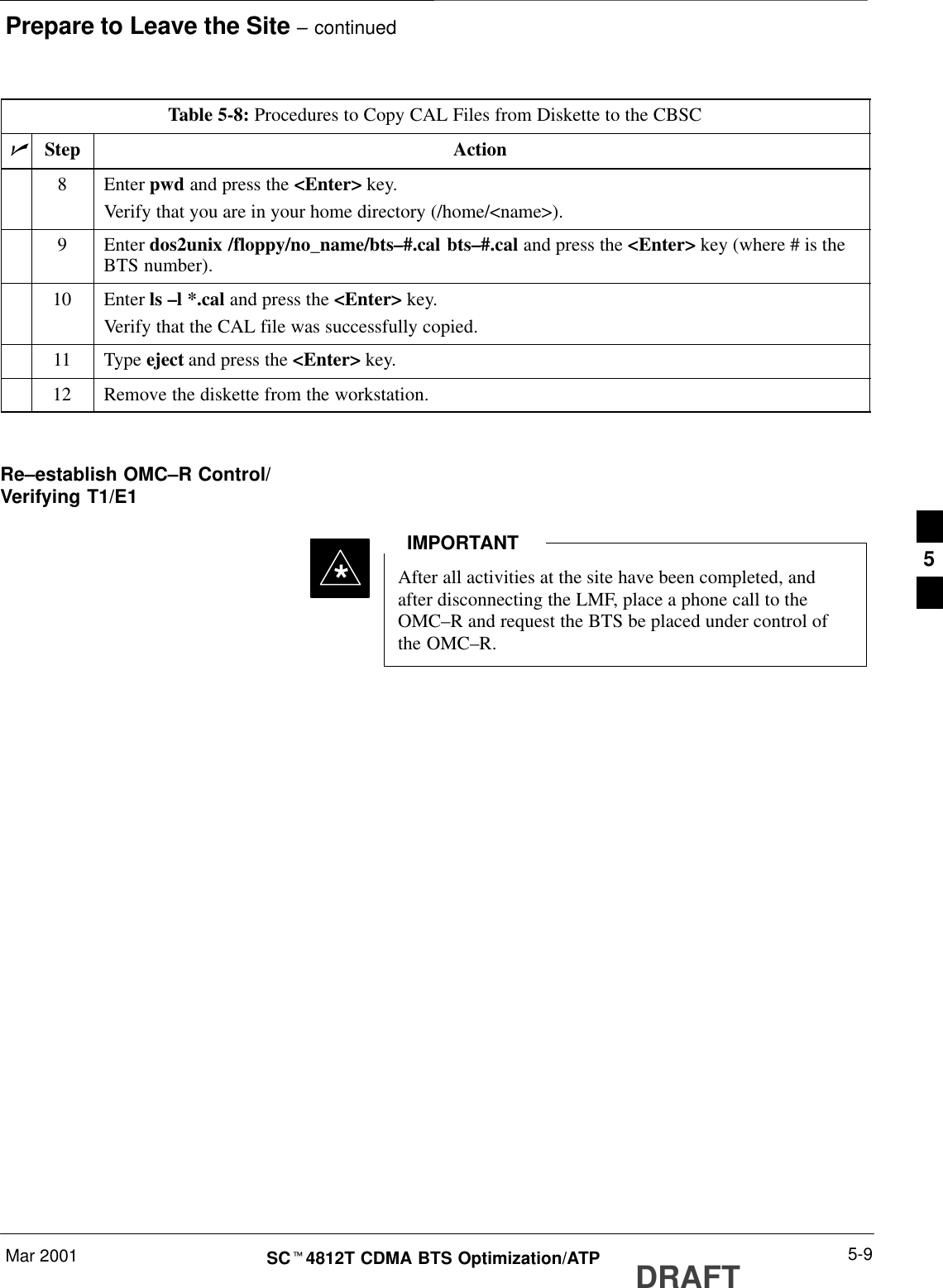
Prepare to Leave the Site  – continuedDRAFTSCt4812T CDMA BTS Optimization/ATP Mar 20015-8LMF RemovalDO NOT power down the LMF without performing theprocedure indicated below. Corrupted/lost data files mayresult, and in some cases, the LMF may lock up.CAUTIONFollow the procedure in Table 5-7 to terminate the LMF session andremove the terminal.Table 5-7: LMF Termination and RemovalnStep Action1From the CDMA window select File>Exit.2From the Windows Task Bar click Start>Shutdown.Click Yes when the Shut Down Windows message appears.3Disconnect the LMF terminal Ethernet connector from the BTS cabinet.4Disconnect the LMF serial port, the RS-232 to GPIB interface box, and the GPIB cables asrequired for equipment transport.Copying CAL Files from Diskette to the CBSCFollow the procedure in Table 5-8 to copy CAL files from a diskette tothe CBSC.Table 5-8: Procedures to Copy CAL Files from Diskette to the CBSCnStep Action1Login to the CBSC on the workstation using your account name and password.NOTEEnter the information that appears in bold text.2Place your diskette containing CAL file(s) in the CBSC workstation diskette drive.3 Type eject –q and press the <Enter> key.4 Type mount and press the <Enter> key.Verify that floppy/no_name  is displayed.NOTEIf the eject command has been previously entered, floppy/no_name  will be appended with anumber. Use the explicit floppy/no_name  reference displayed.5 Enter cd /floppy/no_name and press the <Enter> key.6 Enter ls –lia and press the <Enter> key.Verify that the bts–#.cal file is on the diskette.7 Enter cd and press the <Enter> key.. . . continued on next page5
Prepare to Leave the Site – continuedMar 2001 5-9SCt4812T CDMA BTS Optimization/ATP DRAFTTable 5-8: Procedures to Copy CAL Files from Diskette to the CBSCnActionStep8 Enter pwd and press the <Enter> key.Verify that you are in your home directory (/home/<name>).9 Enter dos2unix /floppy/no_name/bts–#.cal bts–#.cal and press the <Enter> key (where # is theBTS number).10 Enter ls –l *.cal and press the <Enter> key.Verify that the CAL file was successfully copied.11 Type eject and press the <Enter> key.12 Remove the diskette from the workstation. Re–establish OMC–R Control/Verifying T1/E1After all activities at the site have been completed, andafter disconnecting the LMF, place a phone call to theOMC–R and request the BTS be placed under control ofthe OMC–R.IMPORTANT*5
Prepare to Leave the Site  – continuedDRAFTSCt4812T CDMA BTS Optimization/ATP Mar 20015-10Notes5
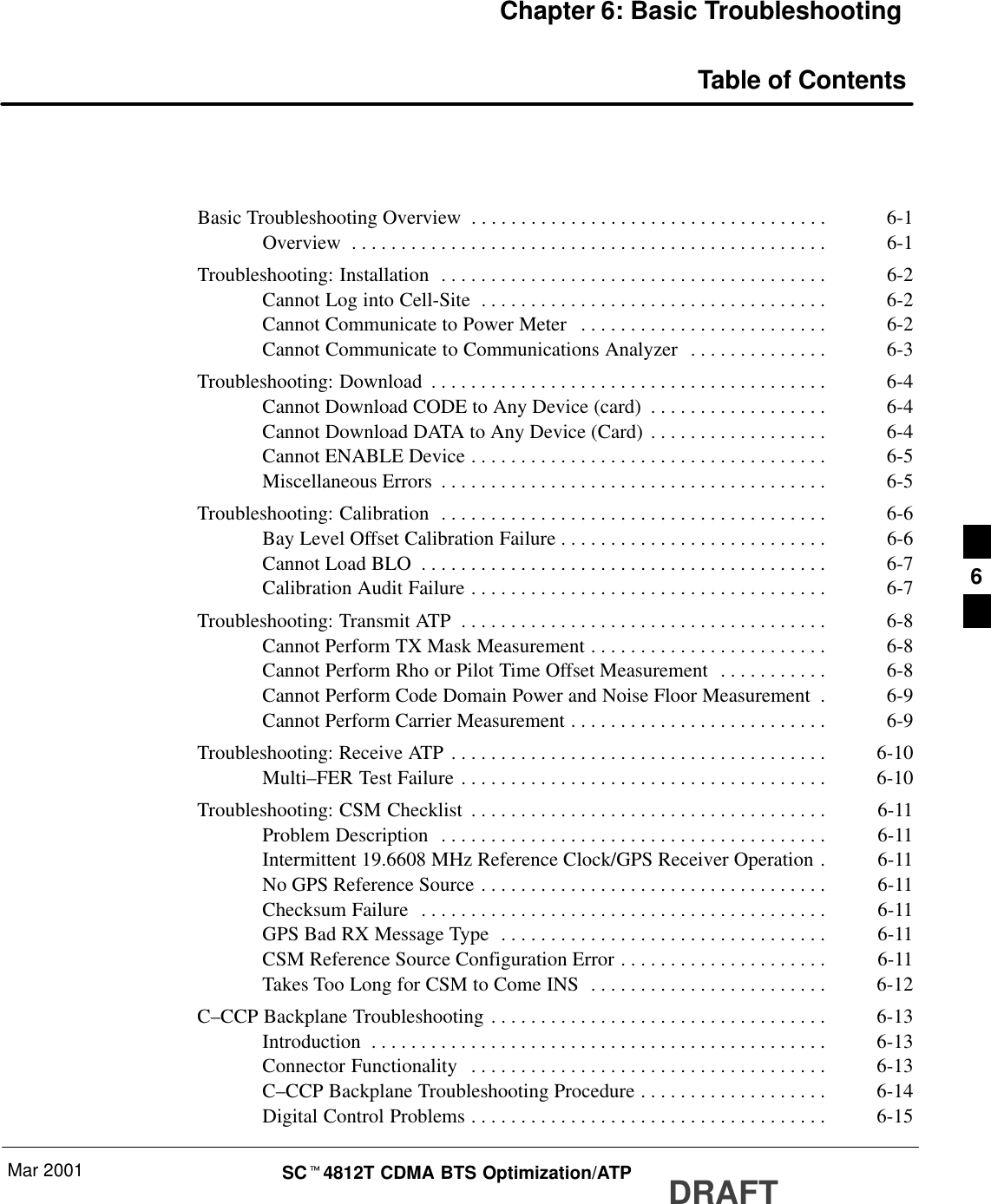
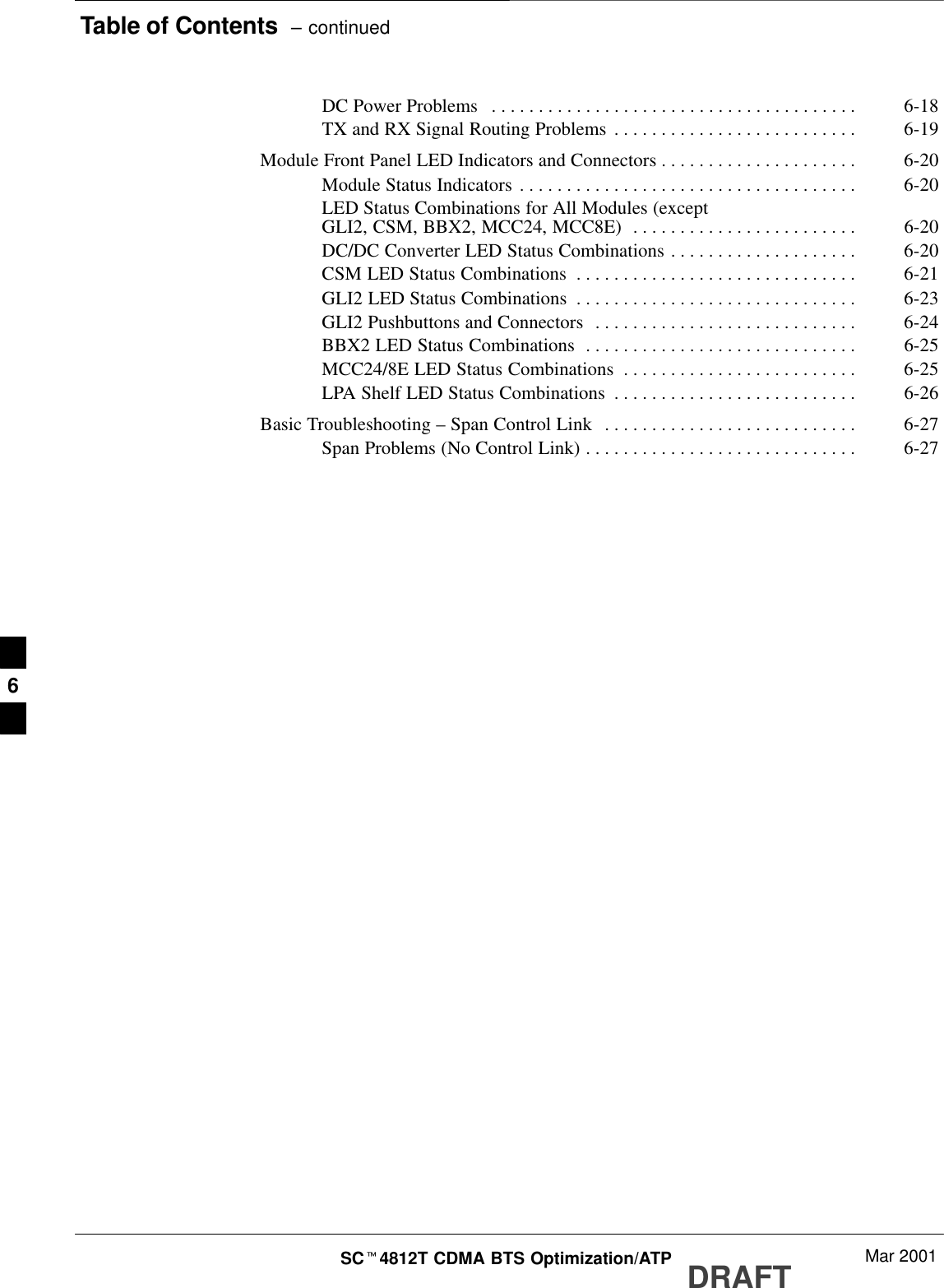
Mar 2001 SCt4812T CDMA BTS Optimization/ATP DRAFTChapter 6: Basic TroubleshootingTable of ContentsBasic Troubleshooting Overview 6-1. . . . . . . . . . . . . . . . . . . . . . . . . . . . . . . . . . . . Overview 6-1. . . . . . . . . . . . . . . . . . . . . . . . . . . . . . . . . . . . . . . . . . . . . . . . Troubleshooting: Installation 6-2. . . . . . . . . . . . . . . . . . . . . . . . . . . . . . . . . . . . . . . Cannot Log into Cell-Site 6-2. . . . . . . . . . . . . . . . . . . . . . . . . . . . . . . . . . . Cannot Communicate to Power Meter 6-2. . . . . . . . . . . . . . . . . . . . . . . . . Cannot Communicate to Communications Analyzer 6-3. . . . . . . . . . . . . . Troubleshooting: Download 6-4. . . . . . . . . . . . . . . . . . . . . . . . . . . . . . . . . . . . . . . . Cannot Download CODE to Any Device (card) 6-4. . . . . . . . . . . . . . . . . . Cannot Download DATA to Any Device (Card) 6-4. . . . . . . . . . . . . . . . . . Cannot ENABLE Device 6-5. . . . . . . . . . . . . . . . . . . . . . . . . . . . . . . . . . . . Miscellaneous Errors 6-5. . . . . . . . . . . . . . . . . . . . . . . . . . . . . . . . . . . . . . . Troubleshooting: Calibration 6-6. . . . . . . . . . . . . . . . . . . . . . . . . . . . . . . . . . . . . . . Bay Level Offset Calibration Failure 6-6. . . . . . . . . . . . . . . . . . . . . . . . . . . Cannot Load BLO 6-7. . . . . . . . . . . . . . . . . . . . . . . . . . . . . . . . . . . . . . . . . Calibration Audit Failure 6-7. . . . . . . . . . . . . . . . . . . . . . . . . . . . . . . . . . . . Troubleshooting: Transmit ATP 6-8. . . . . . . . . . . . . . . . . . . . . . . . . . . . . . . . . . . . . Cannot Perform TX Mask Measurement 6-8. . . . . . . . . . . . . . . . . . . . . . . . Cannot Perform Rho or Pilot Time Offset Measurement 6-8. . . . . . . . . . . Cannot Perform Code Domain Power and Noise Floor Measurement 6-9. Cannot Perform Carrier Measurement 6-9. . . . . . . . . . . . . . . . . . . . . . . . . . Troubleshooting: Receive ATP 6-10. . . . . . . . . . . . . . . . . . . . . . . . . . . . . . . . . . . . . . Multi–FER Test Failure 6-10. . . . . . . . . . . . . . . . . . . . . . . . . . . . . . . . . . . . . Troubleshooting: CSM Checklist 6-11. . . . . . . . . . . . . . . . . . . . . . . . . . . . . . . . . . . . Problem Description 6-11. . . . . . . . . . . . . . . . . . . . . . . . . . . . . . . . . . . . . . . Intermittent 19.6608 MHz Reference Clock/GPS Receiver Operation 6-11. No GPS Reference Source 6-11. . . . . . . . . . . . . . . . . . . . . . . . . . . . . . . . . . . Checksum Failure 6-11. . . . . . . . . . . . . . . . . . . . . . . . . . . . . . . . . . . . . . . . . GPS Bad RX Message Type 6-11. . . . . . . . . . . . . . . . . . . . . . . . . . . . . . . . . CSM Reference Source Configuration Error 6-11. . . . . . . . . . . . . . . . . . . . . Takes Too Long for CSM to Come INS 6-12. . . . . . . . . . . . . . . . . . . . . . . . C–CCP Backplane Troubleshooting 6-13. . . . . . . . . . . . . . . . . . . . . . . . . . . . . . . . . . Introduction 6-13. . . . . . . . . . . . . . . . . . . . . . . . . . . . . . . . . . . . . . . . . . . . . . Connector Functionality 6-13. . . . . . . . . . . . . . . . . . . . . . . . . . . . . . . . . . . . C–CCP Backplane Troubleshooting Procedure 6-14. . . . . . . . . . . . . . . . . . . Digital Control Problems 6-15. . . . . . . . . . . . . . . . . . . . . . . . . . . . . . . . . . . . 6
Table of Contents  – continuedDRAFTSCt4812T CDMA BTS Optimization/ATP Mar 2001DC Power Problems 6-18. . . . . . . . . . . . . . . . . . . . . . . . . . . . . . . . . . . . . . . TX and RX Signal Routing Problems 6-19. . . . . . . . . . . . . . . . . . . . . . . . . . Module Front Panel LED Indicators and Connectors 6-20. . . . . . . . . . . . . . . . . . . . . Module Status Indicators 6-20. . . . . . . . . . . . . . . . . . . . . . . . . . . . . . . . . . . . LED Status Combinations for All Modules (exceptGLI2, CSM, BBX2, MCC24, MCC8E) 6-20. . . . . . . . . . . . . . . . . . . . . . . . DC/DC Converter LED Status Combinations 6-20. . . . . . . . . . . . . . . . . . . . CSM LED Status Combinations 6-21. . . . . . . . . . . . . . . . . . . . . . . . . . . . . . GLI2 LED Status Combinations 6-23. . . . . . . . . . . . . . . . . . . . . . . . . . . . . . GLI2 Pushbuttons and Connectors 6-24. . . . . . . . . . . . . . . . . . . . . . . . . . . . BBX2 LED Status Combinations 6-25. . . . . . . . . . . . . . . . . . . . . . . . . . . . . MCC24/8E LED Status Combinations 6-25. . . . . . . . . . . . . . . . . . . . . . . . . LPA Shelf LED Status Combinations 6-26. . . . . . . . . . . . . . . . . . . . . . . . . . Basic Troubleshooting – Span Control Link 6-27. . . . . . . . . . . . . . . . . . . . . . . . . . . Span Problems (No Control Link) 6-27. . . . . . . . . . . . . . . . . . . . . . . . . . . . . 6
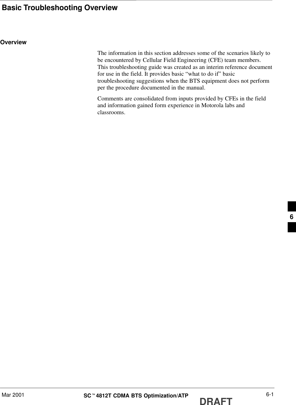
Basic Troubleshooting OverviewMar 2001 6-1SCt4812T CDMA BTS Optimization/ATP DRAFTOverviewThe information in this section addresses some of the scenarios likely tobe encountered by Cellular Field Engineering (CFE) team members.This troubleshooting guide was created as an interim reference documentfor use in the field. It provides basic “what to do if” basictroubleshooting suggestions when the BTS equipment does not performper the procedure documented in the manual.Comments are consolidated from inputs provided by CFEs in the fieldand information gained form experience in Motorola labs andclassrooms.6
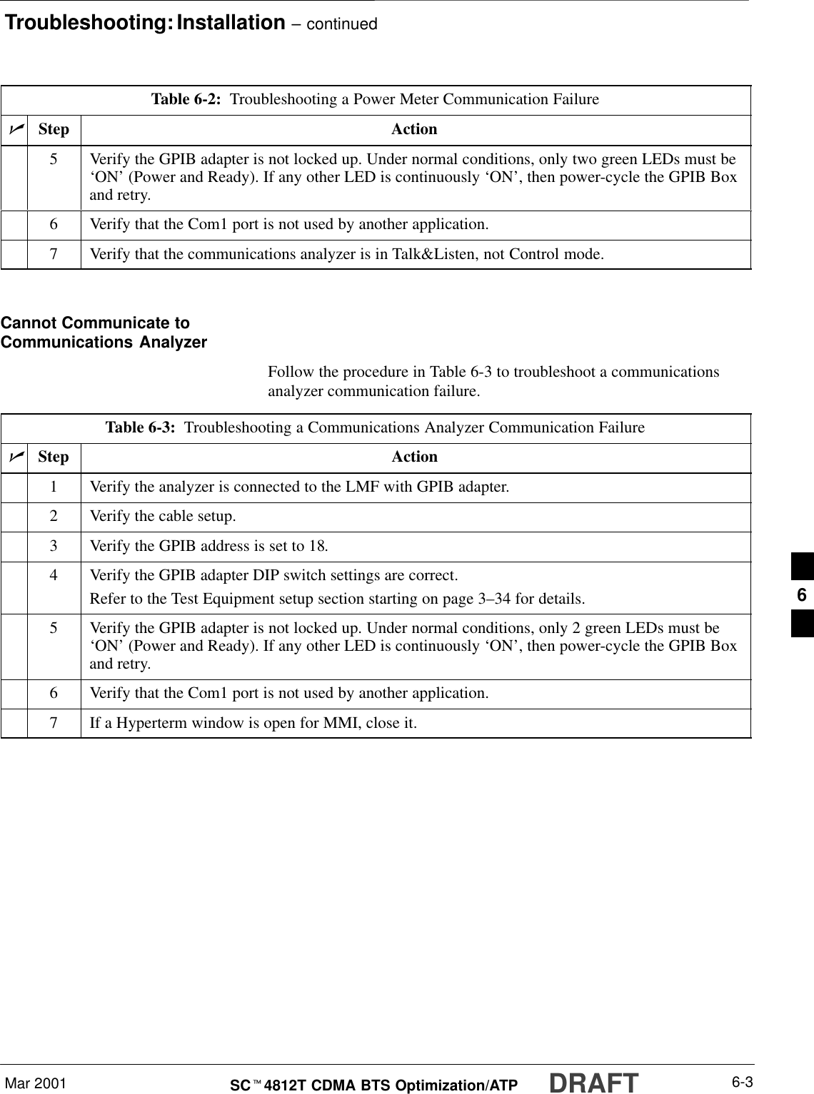
Troubleshooting: InstallationDRAFTSCt4812T CDMA BTS Optimization/ATP Mar 20016-2Cannot Log into Cell-SiteFollow the procedure in Table 6-1 to troubleshoot a login failure.Table 6-1: Login Failure Troubleshooting ProceduresnStep Action1If MGLI2 LED is solid RED, it implies a hardware failure. Reset MGLI2 by re-seating it. If thispersists, install a known good MGLI2 card in MGLI2 slot and retry. A Red LED may also indicateno Ethernet termination at top of frame.2Verify that T1 is disconnected (see Table 3-1 on page 3-4).If T1 is still connected, verify the CBSC has disabled the BTS.3Try pinging the MGLI2 (see Table 3-6 on page 3-15).4Verify the LMF is connected to the Primary LMF port (LAN A) in the front of the BTS (seeTable 3-2 on page 3-5).5Verify the LMF was configured properly (see Preparing the LMF section starting on page 3–6).6Verify the BTS-LMF cable is RG-58 [flexible black cable of less than 76 cm (2.5 feet) length].7Verify the Ethernet ports are terminated properly (see Figure 3-4 on page 3-14).8Verify a T-adapter is not used on the LMF side port if connected to the BTS front LMF primaryport.9Try connecting to the I/O panel (top of frame). Use BNC T-adapters at the LMF port for thisconnection.10 Re-boot the LMF and retry.11 Re-seat the MGLI2 and retry.12 Verify IP addresses are configured properly.Cannot Communicate toPower MeterFollow the procedure in Table 6-2 to troubleshoot a power metercommunication failure.Table 6-2:  Troubleshooting a Power Meter Communication FailurenStep Action1Verify the Power Meter is connected to the LMF with a GPIB adapter.2Verify the cable setup as specified in Chapter 3.3Verify the GPIB address of the Power Meter is set to 13.4Verify the GPIB adapter DIP switch settings are correct.Refer to the Test Equipment setup section for details.. . . continued on next page6
Troubleshooting: Installation – continuedMar 2001 6-3SCt4812T CDMA BTS Optimization/ATP DRAFTTable 6-2:  Troubleshooting a Power Meter Communication FailurenActionStep5Verify the GPIB adapter is not locked up. Under normal conditions, only two green LEDs must be‘ON’ (Power and Ready). If any other LED is continuously ‘ON’, then power-cycle the GPIB Boxand retry.6Verify that the Com1 port is not used by another application.7Verify that the communications analyzer is in Talk&Listen, not Control mode. Cannot Communicate toCommunications AnalyzerFollow the procedure in Table 6-3 to troubleshoot a communicationsanalyzer communication failure.Table 6-3:  Troubleshooting a Communications Analyzer Communication FailurenStep Action1Verify the analyzer is connected to the LMF with GPIB adapter.2Verify the cable setup.3Verify the GPIB address is set to 18.4Verify the GPIB adapter DIP switch settings are correct.Refer to the Test Equipment setup section starting on page 3–34 for details.5Verify the GPIB adapter is not locked up. Under normal conditions, only 2 green LEDs must be‘ON’ (Power and Ready). If any other LED is continuously ‘ON’, then power-cycle the GPIB Boxand retry.6Verify that the Com1 port is not used by another application.7If a Hyperterm window is open for MMI, close it.6
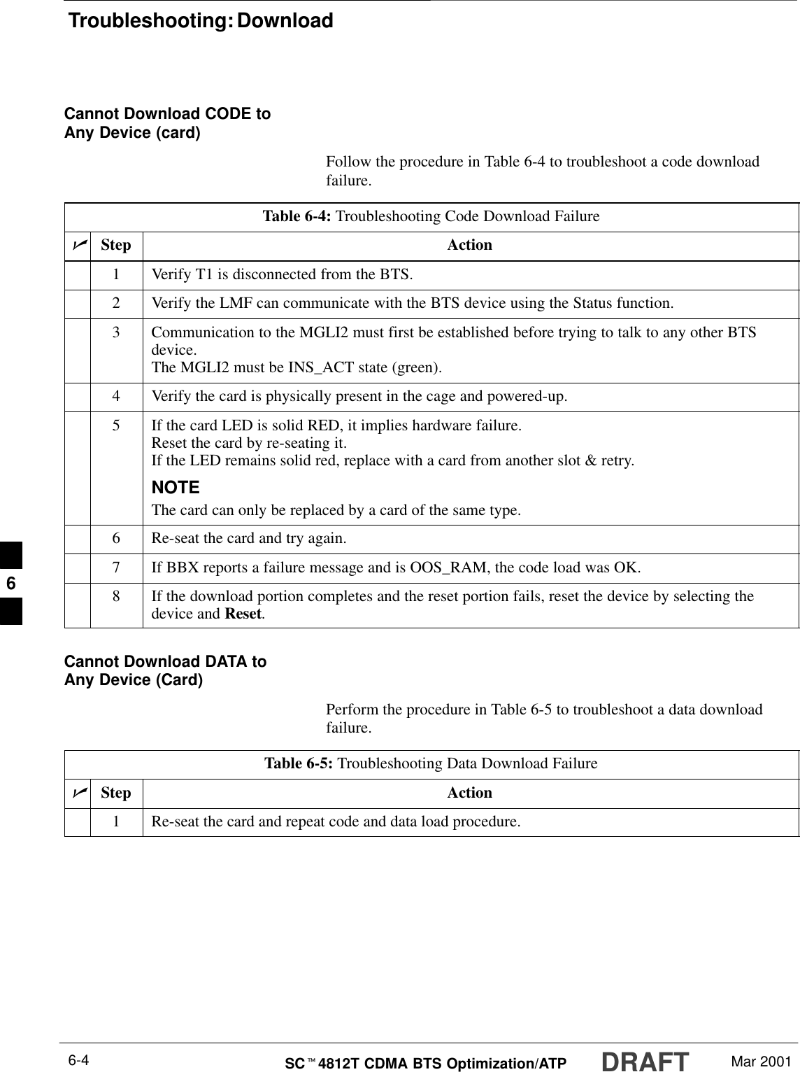
Troubleshooting: DownloadDRAFTSCt4812T CDMA BTS Optimization/ATP Mar 20016-4Cannot Download CODE toAny Device (card)Follow the procedure in Table 6-4 to troubleshoot a code downloadfailure.Table 6-4: Troubleshooting Code Download FailurenStep Action1Verify T1 is disconnected from the BTS.2Verify the LMF can communicate with the BTS device using the Status function.3Communication to the MGLI2 must first be established before trying to talk to any other BTSdevice.The MGLI2 must be INS_ACT state (green).4Verify the card is physically present in the cage and powered-up.5If the card LED is solid RED, it implies hardware failure.Reset the card by re-seating it.If the LED remains solid red, replace with a card from another slot & retry.NOTEThe card can only be replaced by a card of the same type.6Re-seat the card and try again.7If BBX reports a failure message and is OOS_RAM, the code load was OK.8If the download portion completes and the reset portion fails, reset the device by selecting thedevice and Reset.Cannot Download DATA toAny Device (Card)Perform the procedure in Table 6-5 to troubleshoot a data downloadfailure.Table 6-5: Troubleshooting Data Download FailurenStep Action1Re-seat the card and repeat code and data load procedure.6
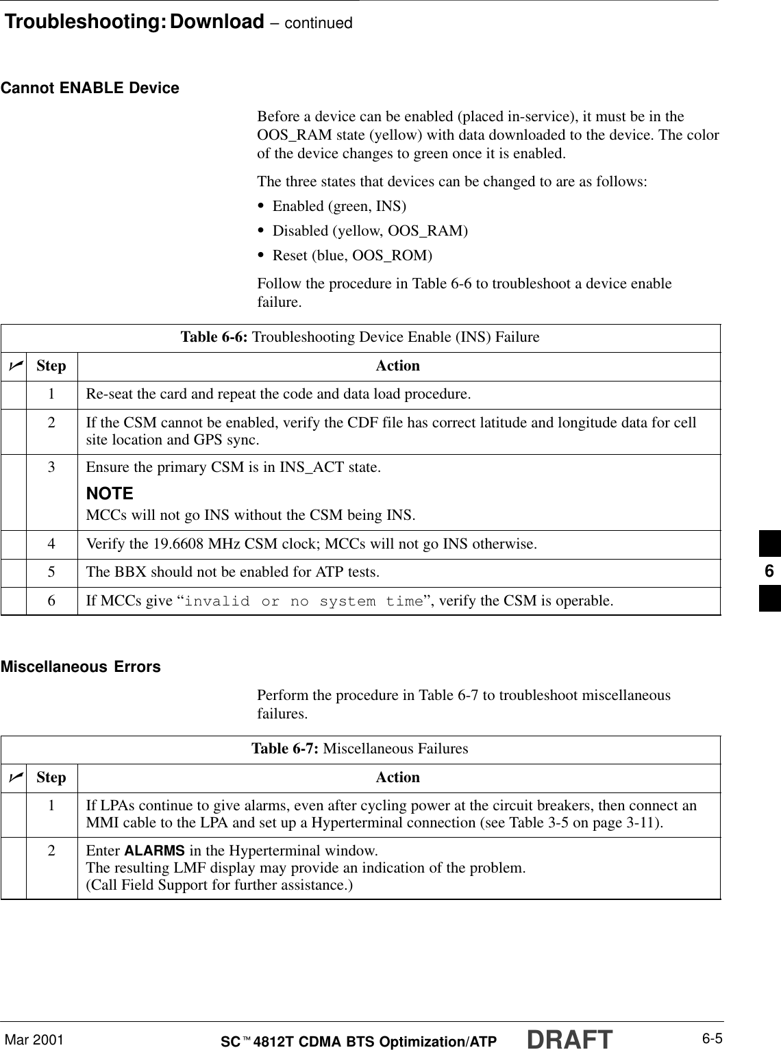
Troubleshooting: Download – continuedMar 2001 6-5SCt4812T CDMA BTS Optimization/ATP DRAFTCannot ENABLE DeviceBefore a device can be enabled (placed in-service), it must be in theOOS_RAM state (yellow) with data downloaded to the device. The colorof the device changes to green once it is enabled.The three states that devices can be changed to are as follows:SEnabled (green, INS)SDisabled (yellow, OOS_RAM)SReset (blue, OOS_ROM)Follow the procedure in Table 6-6 to troubleshoot a device enablefailure.Table 6-6: Troubleshooting Device Enable (INS) FailurenStep Action1Re-seat the card and repeat the code and data load procedure.2If the CSM cannot be enabled, verify the CDF file has correct latitude and longitude data for cellsite location and GPS sync.3Ensure the primary CSM is in INS_ACT state.NOTEMCCs will not go INS without the CSM being INS.4Verify the 19.6608 MHz CSM clock; MCCs will not go INS otherwise.5The BBX should not be enabled for ATP tests.6If MCCs give “invalid or no system time”, verify the CSM is operable. Miscellaneous ErrorsPerform the procedure in Table 6-7 to troubleshoot miscellaneousfailures.Table 6-7: Miscellaneous FailuresnStep Action1If LPAs continue to give alarms, even after cycling power at the circuit breakers, then connect anMMI cable to the LPA and set up a Hyperterminal connection (see Table 3-5 on page 3-11).2 Enter ALARMS in the Hyperterminal window.The resulting LMF display may provide an indication of the problem.(Call Field Support for further assistance.)6
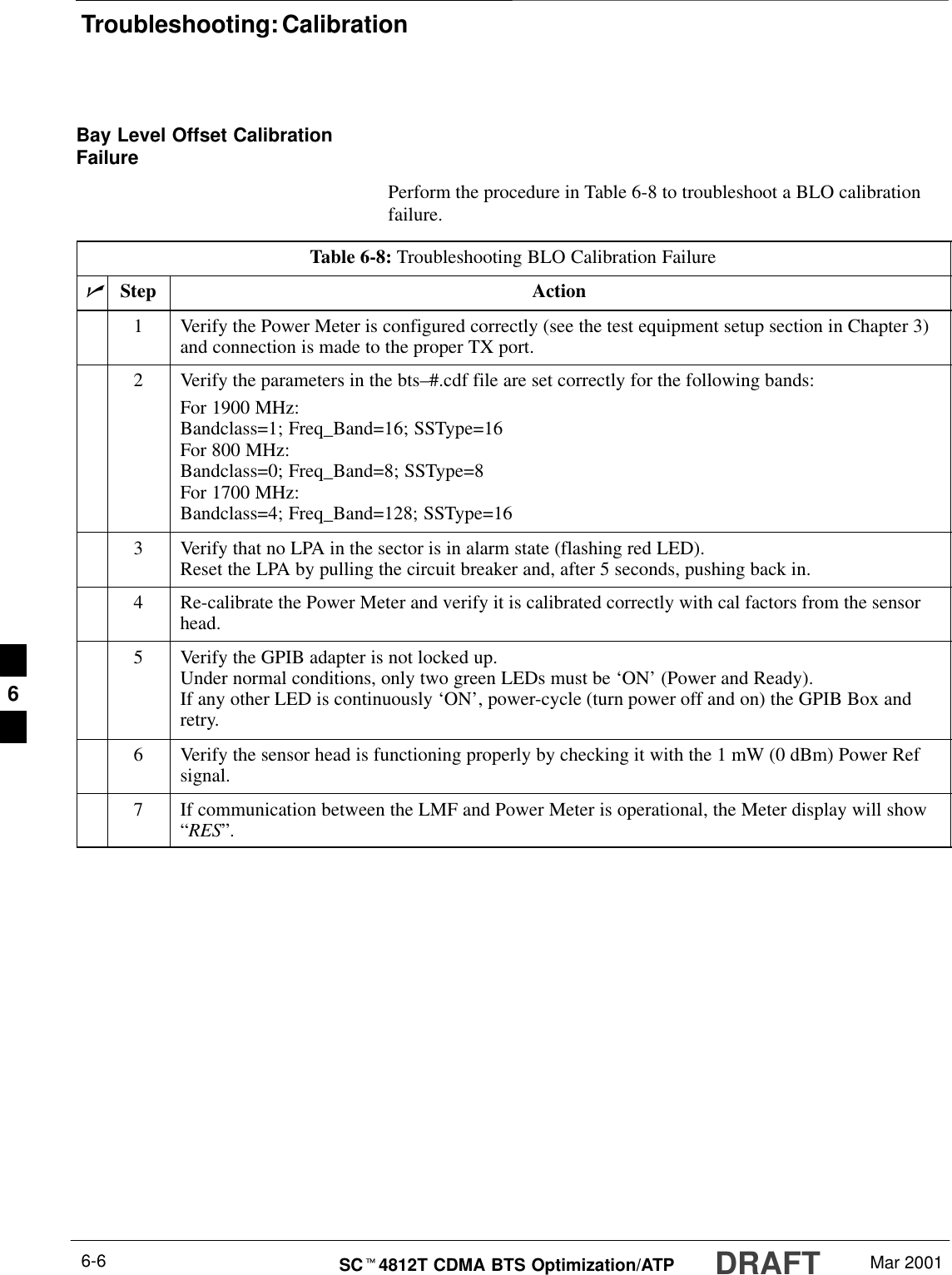
Troubleshooting: CalibrationDRAFTSCt4812T CDMA BTS Optimization/ATP Mar 20016-6Bay Level Offset CalibrationFailurePerform the procedure in Table 6-8 to troubleshoot a BLO calibrationfailure.Table 6-8: Troubleshooting BLO Calibration FailurenStep Action1Verify the Power Meter is configured correctly (see the test equipment setup section in Chapter 3)and connection is made to the proper TX port.2Verify the parameters in the bts–#.cdf file are set correctly for the following bands:For 1900 MHz:Bandclass=1; Freq_Band=16; SSType=16For 800 MHz:Bandclass=0; Freq_Band=8; SSType=8For 1700 MHz:Bandclass=4; Freq_Band=128; SSType=163Verify that no LPA in the sector is in alarm state (flashing red LED).Reset the LPA by pulling the circuit breaker and, after 5 seconds, pushing back in.4Re-calibrate the Power Meter and verify it is calibrated correctly with cal factors from the sensorhead.5Verify the GPIB adapter is not locked up.Under normal conditions, only two green LEDs must be ‘ON’ (Power and Ready).If any other LED is continuously ‘ON’, power-cycle (turn power off and on) the GPIB Box andretry.6Verify the sensor head is functioning properly by checking it with the 1 mW (0 dBm) Power Refsignal.7If communication between the LMF and Power Meter is operational, the Meter display will show“RES”. 6
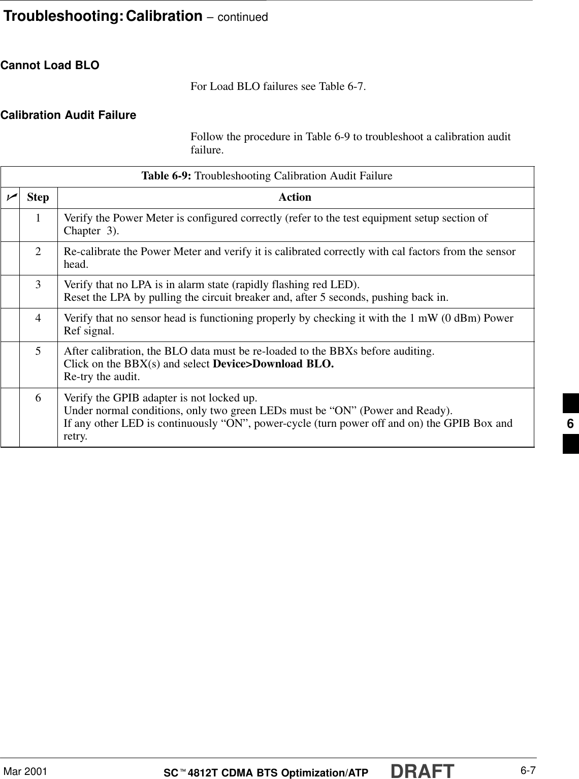
Troubleshooting: Calibration – continuedMar 2001 6-7SCt4812T CDMA BTS Optimization/ATP DRAFTCannot Load BLOFor Load BLO failures see Table 6-7.Calibration Audit FailureFollow the procedure in Table 6-9 to troubleshoot a calibration auditfailure.Table 6-9: Troubleshooting Calibration Audit FailurenStep Action1Verify the Power Meter is configured correctly (refer to the test equipment setup section ofChapter  3).2Re-calibrate the Power Meter and verify it is calibrated correctly with cal factors from the sensorhead.3Verify that no LPA is in alarm state (rapidly flashing red LED).Reset the LPA by pulling the circuit breaker and, after 5 seconds, pushing back in.4Verify that no sensor head is functioning properly by checking it with the 1 mW (0 dBm) PowerRef signal.5After calibration, the BLO data must be re-loaded to the BBXs before auditing.Click on the BBX(s) and select Device>Download BLO.Re-try the audit.6Verify the GPIB adapter is not locked up.Under normal conditions, only two green LEDs must be “ON” (Power and Ready).If any other LED is continuously “ON”, power-cycle (turn power off and on) the GPIB Box andretry. 6
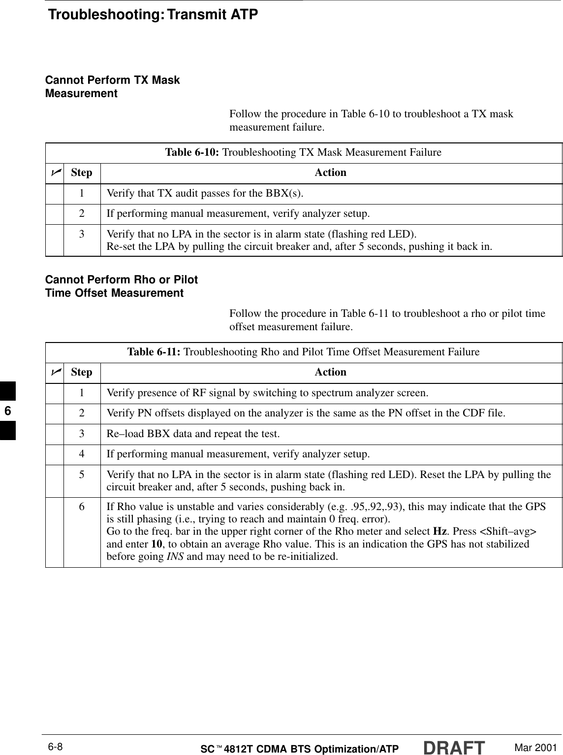
Troubleshooting: Transmit ATPDRAFTSCt4812T CDMA BTS Optimization/ATP Mar 20016-8Cannot Perform TX MaskMeasurementFollow the procedure in Table 6-10 to troubleshoot a TX maskmeasurement failure.Table 6-10: Troubleshooting TX Mask Measurement FailurenStep Action1Verify that TX audit passes for the BBX(s).2If performing manual measurement, verify analyzer setup.3Verify that no LPA in the sector is in alarm state (flashing red LED).Re-set the LPA by pulling the circuit breaker and, after 5 seconds, pushing it back in.Cannot Perform Rho or PilotTime Offset MeasurementFollow the procedure in Table 6-11 to troubleshoot a rho or pilot timeoffset measurement failure.Table 6-11: Troubleshooting Rho and Pilot Time Offset Measurement FailurenStep Action1Verify presence of RF signal by switching to spectrum analyzer screen.2Verify PN offsets displayed on the analyzer is the same as the PN offset in the CDF file.3 Re–load BBX data and repeat the test.4If performing manual measurement, verify analyzer setup.5Verify that no LPA in the sector is in alarm state (flashing red LED). Reset the LPA by pulling thecircuit breaker and, after 5 seconds, pushing back in.6If Rho value is unstable and varies considerably (e.g. .95,.92,.93), this may indicate that the GPSis still phasing (i.e., trying to reach and maintain 0 freq. error).Go to the freq. bar in the upper right corner of the Rho meter and select Hz. Press <Shift–avg>and enter 10, to obtain an average Rho value. This is an indication the GPS has not stabilizedbefore going INS and may need to be re-initialized. 6
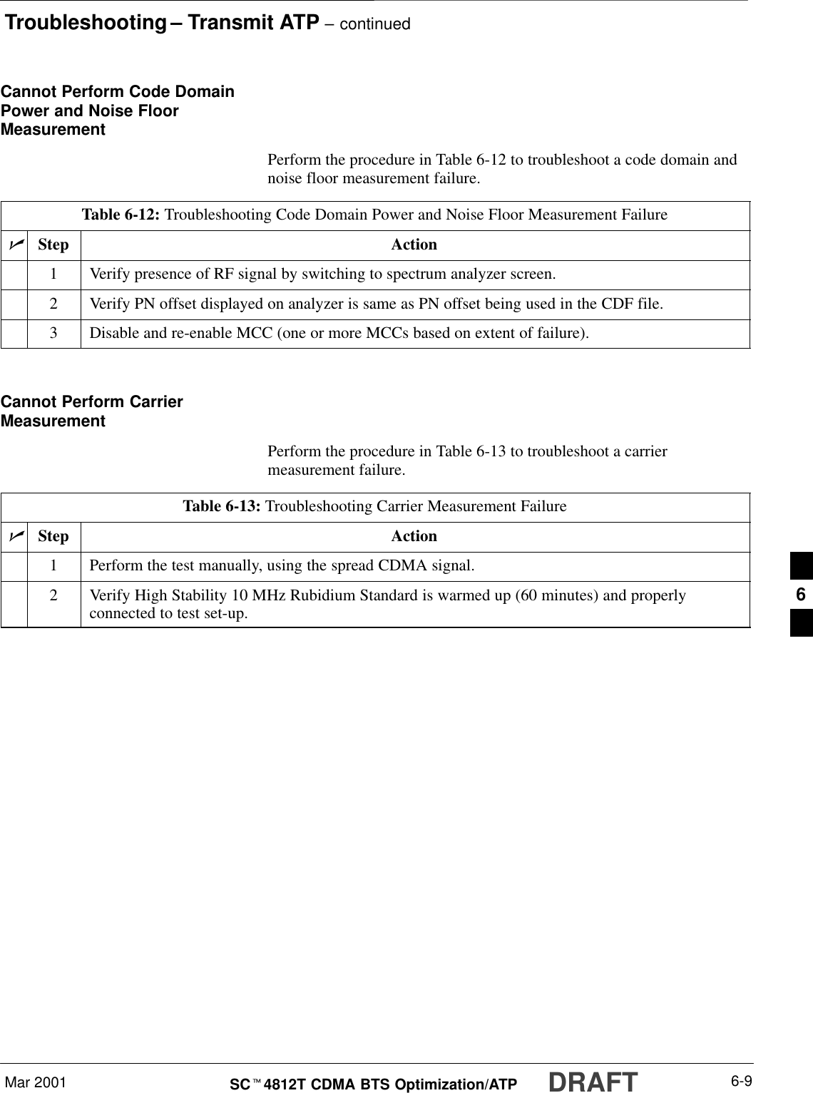
Troubleshooting – Transmit ATP – continuedMar 2001 6-9SCt4812T CDMA BTS Optimization/ATP DRAFTCannot Perform Code DomainPower and Noise FloorMeasurementPerform the procedure in Table 6-12 to troubleshoot a code domain andnoise floor measurement failure.Table 6-12: Troubleshooting Code Domain Power and Noise Floor Measurement FailurenStep Action1Verify presence of RF signal by switching to spectrum analyzer screen.2Verify PN offset displayed on analyzer is same as PN offset being used in the CDF file.3Disable and re-enable MCC (one or more MCCs based on extent of failure). Cannot Perform CarrierMeasurementPerform the procedure in Table 6-13 to troubleshoot a carriermeasurement failure.Table 6-13: Troubleshooting Carrier Measurement FailurenStep Action1Perform the test manually, using the spread CDMA signal.2Verify High Stability 10 MHz Rubidium Standard is warmed up (60 minutes) and properlyconnected to test set-up. 6
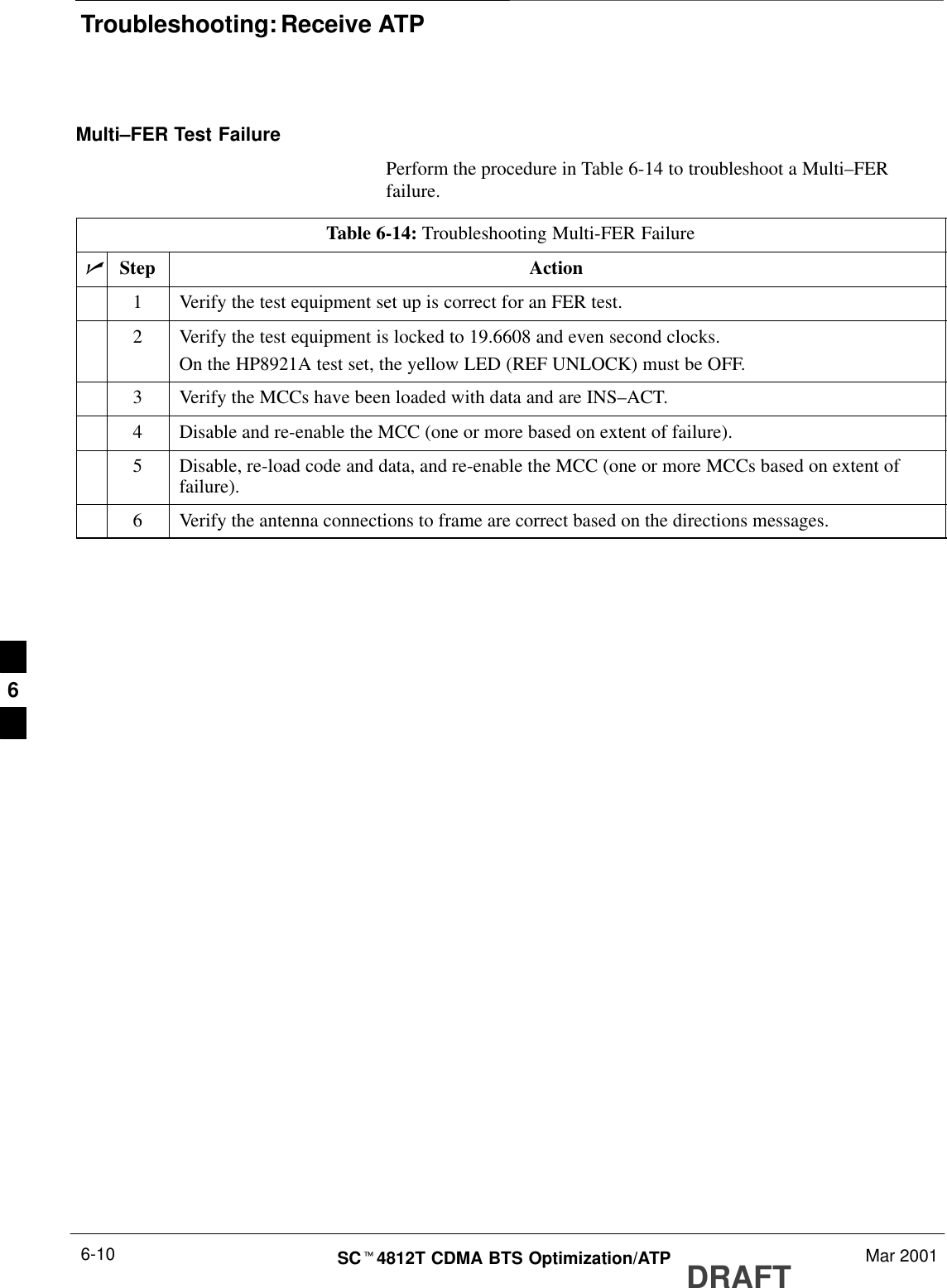
Troubleshooting: Receive ATPDRAFTSCt4812T CDMA BTS Optimization/ATP Mar 20016-10Multi–FER Test FailurePerform the procedure in Table 6-14 to troubleshoot a Multi–FERfailure.Table 6-14: Troubleshooting Multi-FER FailurenStep Action1Verify the test equipment set up is correct for an FER test.2Verify the test equipment is locked to 19.6608 and even second clocks.On the HP8921A test set, the yellow LED (REF UNLOCK) must be OFF.3Verify the MCCs have been loaded with data and are INS–ACT.4Disable and re-enable the MCC (one or more based on extent of failure).5Disable, re-load code and data, and re-enable the MCC (one or more MCCs based on extent offailure).6Verify the antenna connections to frame are correct based on the directions messages. 6
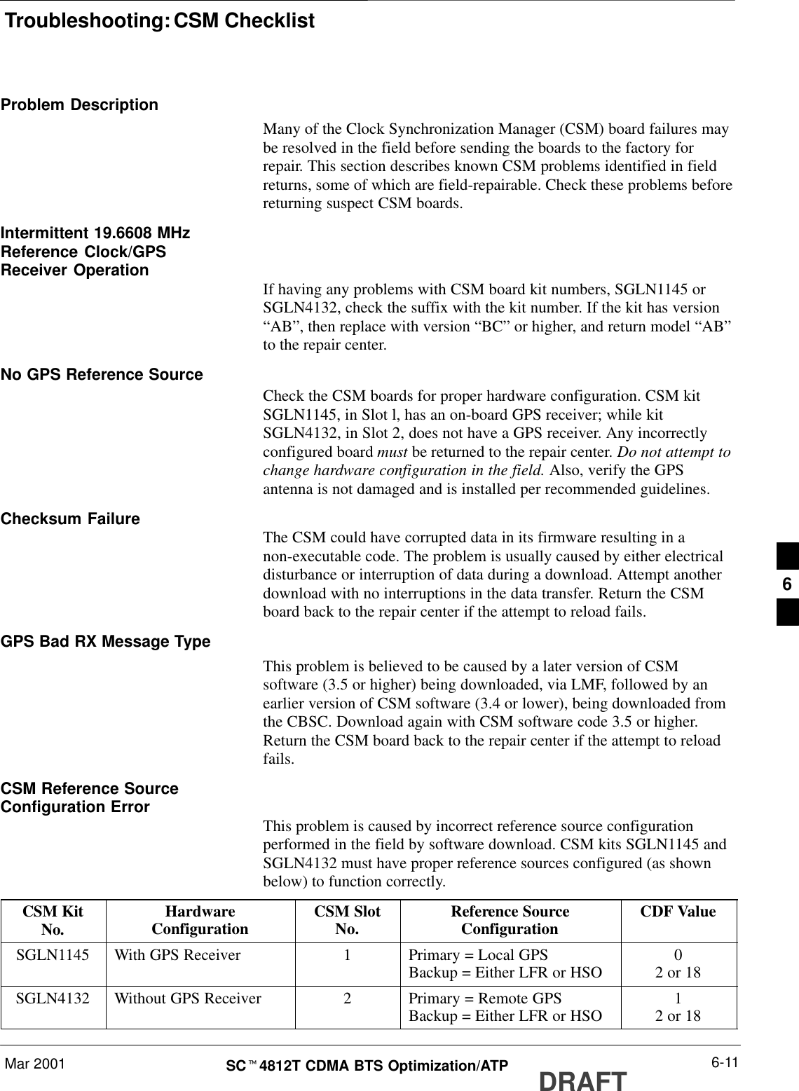
Troubleshooting: CSM ChecklistMar 2001 6-11SCt4812T CDMA BTS Optimization/ATP DRAFTProblem DescriptionMany of the Clock Synchronization Manager (CSM) board failures maybe resolved in the field before sending the boards to the factory forrepair. This section describes known CSM problems identified in fieldreturns, some of which are field-repairable. Check these problems beforereturning suspect CSM boards.Intermittent 19.6608 MHzReference Clock/GPSReceiver Operation If having any problems with CSM board kit numbers, SGLN1145 orSGLN4132, check the suffix with the kit number. If the kit has version“AB”, then replace with version “BC” or higher, and return model “AB”to the repair center.No GPS Reference SourceCheck the CSM boards for proper hardware configuration. CSM kitSGLN1145, in Slot l, has an on-board GPS receiver; while kitSGLN4132, in Slot 2, does not have a GPS receiver. Any incorrectlyconfigured board must be returned to the repair center. Do not attempt tochange hardware configuration in the field. Also, verify the GPSantenna is not damaged and is installed per recommended guidelines.Checksum Failure The CSM could have corrupted data in its firmware resulting in anon-executable code. The problem is usually caused by either electricaldisturbance or interruption of data during a download. Attempt anotherdownload with no interruptions in the data transfer. Return the CSMboard back to the repair center if the attempt to reload fails.GPS Bad RX Message TypeThis problem is believed to be caused by a later version of CSMsoftware (3.5 or higher) being downloaded, via LMF, followed by anearlier version of CSM software (3.4 or lower), being downloaded fromthe CBSC. Download again with CSM software code 3.5 or higher.Return the CSM board back to the repair center if the attempt to reloadfails.CSM Reference SourceConfiguration Error This problem is caused by incorrect reference source configurationperformed in the field by software download. CSM kits SGLN1145 andSGLN4132 must have proper reference sources configured (as shownbelow) to function correctly.CSM KitNo. HardwareConfiguration CSM SlotNo. Reference SourceConfiguration CDF ValueSGLN1145 With GPS Receiver 1Primary = Local GPSBackup = Either LFR or HSO 02 or 18SGLN4132 Without GPS Receiver 2Primary = Remote GPSBackup = Either LFR or HSO 12 or 186
Troubleshooting: CSM Checklist – continuedDRAFTSCt4812T CDMA BTS Optimization/ATP Mar 20016-12Takes Too Long for CSM toCome INSThis problem may be caused by a delay in GPS acquisition. Check theaccuracy flag status and/or current position. Refer to the GSM systemtime/GPS and LFR/HSO verification section in Chapter 3. At least onesatellite should be visible and tracked for the “surveyed” mode and foursatellites should be visible and tracked for the “estimated” mode. Also,verify correct base site position data used in “surveyed” mode.6
C–CCP Backplane TroubleshootingMar 2001 6-13SCt4812T CDMA BTS Optimization/ATP DRAFTIntroductionThe C–CCP backplane is a multi–layer board that interconnects all theC–CCP modules. The complexity of this board lends itself to possibleimproper diagnoses when problems occur.Connector FunctionalityThe following connector overview describes the major types ofbackplane connectors along with the functionality of each. Thisinformation allows the CFE to:SDetermine which connector(s) is associated with a specific problemtype.SIsolate problems to a specific cable or connector.Primary “A” and Redundant “B” Inter Shelf Bus ConnectorsThe 40 pin Inter Shelf Bus (ISB) connectors provide an interface busfrom the master GLI2 to all other GLI2s in the modem frame. Theirbasic function is to provide clock synchronization from the master GLI2to all other GLI2s in the frame.The ISB also provides the following functions:SSpan line grooming when a single span is used for multiple cages.SMMI connection to/from the master GLI2 to cell site modem.SInterface between GLI2s and the AMR (for reporting BTS alarms).Span Line ConnectorThe span line input is an 8–pin RJ–45 connector that provides a primaryand secondary (if used) span line interface to each GLI2 in the C–CCPshelf. The span line is used for MM/EMX switch control of the MasterGLI2 and also all the BBX traffic.Primary “A” and Redundant “B” Reference DistributionModule Input/OutputThe Reference Distribution Module (RDM) connectors route the 3 MHzreference signals from the CSMs to the GLI2s and all BBXs in thebackplane. The signals are used to phase lock loop all clock circuits onthe GLI2s and BBX boards to produce precise clock and signalfrequencies.Power Input (Return A, B, and C connectors)Provides a +27 volt or –48 volt input for use by the power supplymodules. . . . continued on next page6
C–CCP  Backplane Troubleshooting – continuedDRAFTSCt4812T CDMA BTS Optimization/ATP Mar 20016-14Power Supply Module InterfaceEach power supply module has a series of three different connectors toprovide the needed inputs/outputs to the C–CCP backplane. Theseinclude a VCC/Ground input connector, a Harting style multiple pininterface, and a +15 V/Analog Ground output connector. The C–CCPPower Modules convert +27 or –48 Volts to a regulated +15, +6.5, and+5.0 Volts to be used by the C–CCP shelf cards. In the –48 V BTS, theLPA power modules convert –48 Volts to a regulated +27 Volts.GLI2 ConnectorThis connector consists of a Harting 4SU digital connector and a6–conductor coaxial connector for RDM distribution. The connectorsprovide inputs/outputs for the GLI2s in the C–CCP backplane.GLI2 Ethernet “A” and “B” ConnectionsThese BNC connectors are located on the C–CCP backplane and routedto the GLI2 board. This interface provides all the control and datacommunications between the master GLI2 and the other GLI2, betweengateways, and for the LMF on the LAN.BBX ConnectorEach BBX connector consists of a Harting 2SU/1SU digital connectorand two 6–conductor coaxial connectors.  These connectors provide DC,digital, and RF inputs/outputs for the BBXs in the C–CCP backplane.CIO ConnectorsSRX RF antenna path signal inputs are routed through RX Tri–Filters(on the I/O plate), and via coaxial cables to the two MPC modules –the six “A” (main) signals go to one MPC; the six “B” (diversity) tothe other. The MPC outputs the low–noise–amplified signals via theC–CCP backplane to the CIO where the signals are split and sent tothe appropriate BBX.SA digital bus then routes the baseband signal through the BBX, to thebackplane, then on to the MCC slots.SDigital TX antenna path signals originate at the MCCs. Each  outputis routed from the MCC slot via the backplane appropriate BBX.STX RF path signal originates from the BBX, through the backplane tothe CIO, through the CIO, and via multi-conductor coaxial cabling tothe LPAs in the LPA shelf.C–CCP BackplaneTroubleshooting ProcedureTable 6-15 through Table 6-24 provide procedures for troubleshootingproblems that appear to be related to a defective C–CCP backplane. Thetables are broken down into possible problems and steps that should betaken in an attempt to find the root cause. . . . continued on next page6
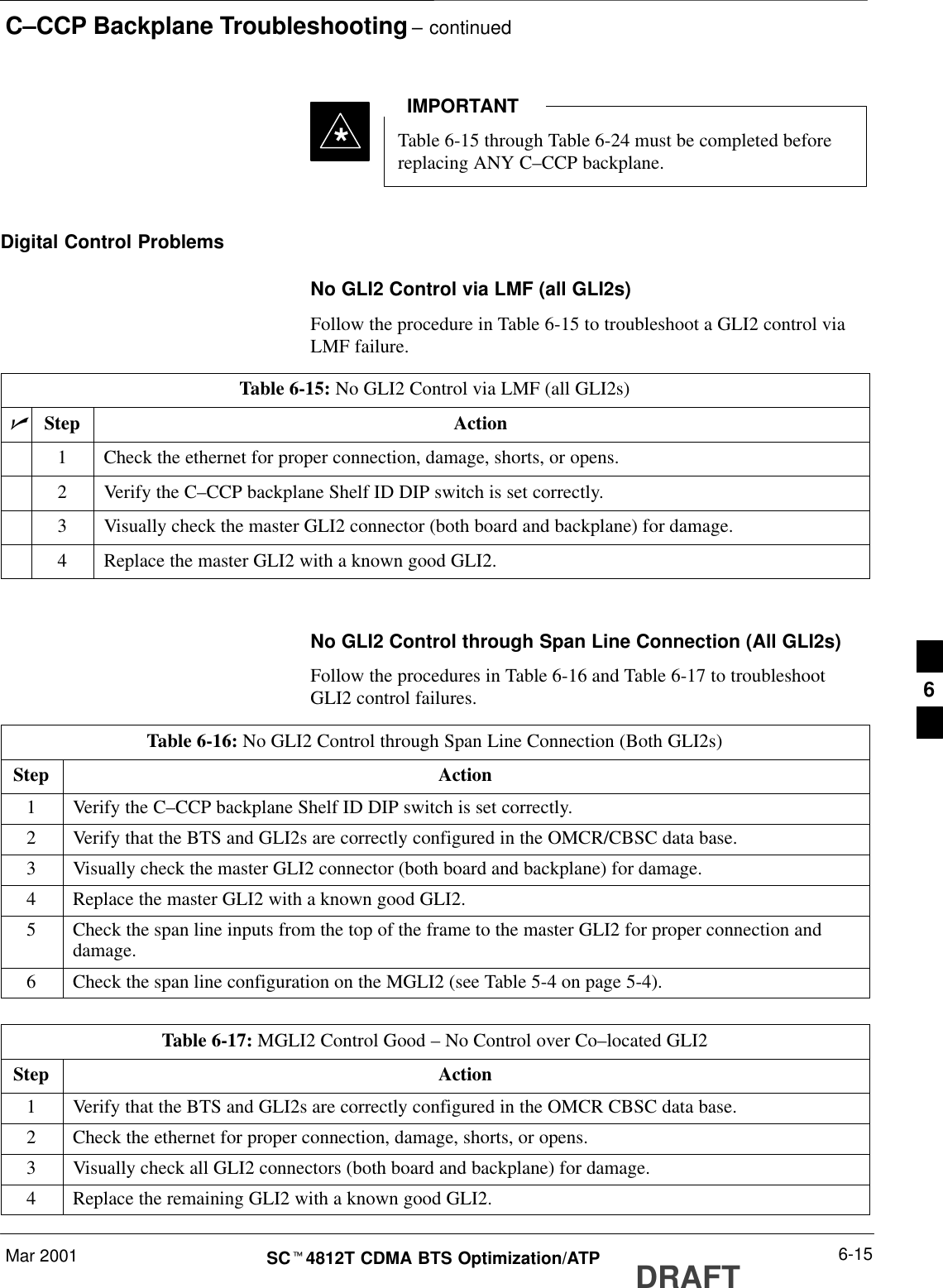
C–CCP Backplane Troubleshooting – continuedMar 2001 6-15SCt4812T CDMA BTS Optimization/ATP DRAFTTable 6-15 through Table 6-24 must be completed beforereplacing ANY C–CCP backplane.IMPORTANT*Digital Control ProblemsNo GLI2 Control via LMF (all GLI2s)Follow the procedure in Table 6-15 to troubleshoot a GLI2 control viaLMF failure.Table 6-15: No GLI2 Control via LMF (all GLI2s)nStep Action1Check the ethernet for proper connection, damage, shorts, or opens.2Verify the C–CCP backplane Shelf ID DIP switch is set correctly.3Visually check the master GLI2 connector (both board and backplane) for damage.4Replace the master GLI2 with a known good GLI2. No GLI2 Control through Span Line Connection (All GLI2s)Follow the procedures in Table 6-16 and Table 6-17 to troubleshootGLI2 control failures.Table 6-16: No GLI2 Control through Span Line Connection (Both GLI2s)Step Action1Verify the C–CCP backplane Shelf ID DIP switch is set correctly.2Verify that the BTS and GLI2s are correctly configured in the OMCR/CBSC data base.3Visually check the master GLI2 connector (both board and backplane) for damage.4Replace the master GLI2 with a known good GLI2.5Check the span line inputs from the top of the frame to the master GLI2 for proper connection anddamage.6Check the span line configuration on the MGLI2 (see Table 5-4 on page 5-4).Table 6-17: MGLI2 Control Good – No Control over Co–located GLI2Step Action1Verify that the BTS and GLI2s are correctly configured in the OMCR CBSC data base.2Check the ethernet for proper connection, damage, shorts, or opens.3Visually check all GLI2 connectors (both board and backplane) for damage.4Replace the remaining GLI2 with a known good GLI2.6
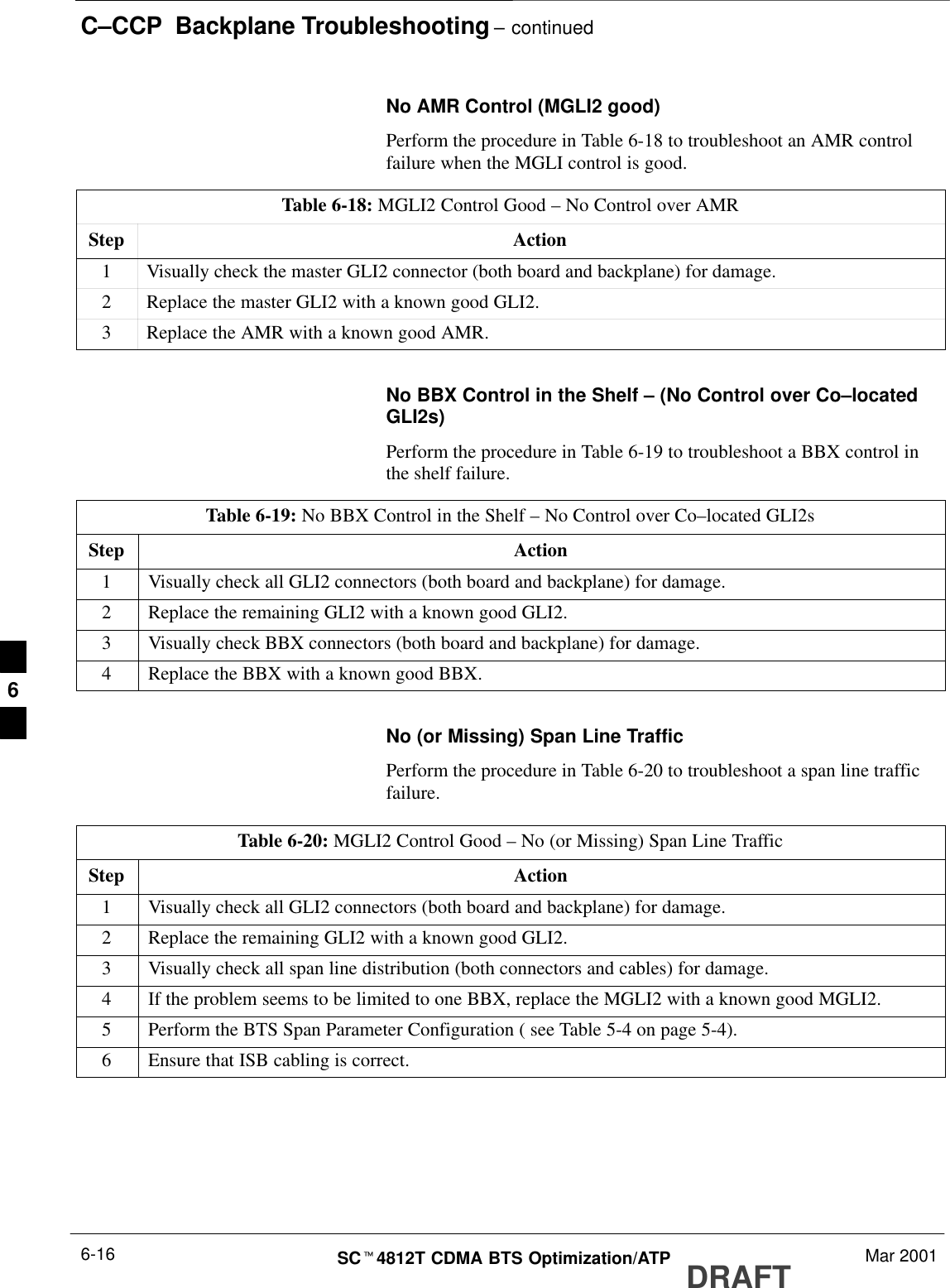
C–CCP  Backplane Troubleshooting – continuedDRAFTSCt4812T CDMA BTS Optimization/ATP Mar 20016-16No AMR Control (MGLI2 good)Perform the procedure in Table 6-18 to troubleshoot an AMR controlfailure when the MGLI control is good.Table 6-18: MGLI2 Control Good – No Control over AMRStep Action1Visually check the master GLI2 connector (both board and backplane) for damage.2Replace the master GLI2 with a known good GLI2.3Replace the AMR with a known good AMR.No BBX Control in the Shelf – (No Control over Co–locatedGLI2s)Perform the procedure in Table 6-19 to troubleshoot a BBX control inthe shelf failure.Table 6-19: No BBX Control in the Shelf – No Control over Co–located GLI2sStep Action1Visually check all GLI2 connectors (both board and backplane) for damage.2Replace the remaining GLI2 with a known good GLI2.3Visually check BBX connectors (both board and backplane) for damage.4Replace the BBX with a known good BBX.No (or Missing) Span Line TrafficPerform the procedure in Table 6-20 to troubleshoot a span line trafficfailure.Table 6-20: MGLI2 Control Good – No (or Missing) Span Line TrafficStep Action1Visually check all GLI2 connectors (both board and backplane) for damage.2Replace the remaining GLI2 with a known good GLI2.3Visually check all span line distribution (both connectors and cables) for damage.4If the problem seems to be limited to one BBX, replace the MGLI2 with a known good MGLI2.5Perform the BTS Span Parameter Configuration ( see Table 5-4 on page 5-4).6Ensure that ISB cabling is correct.6
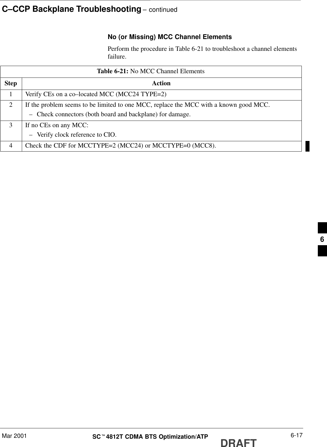
C–CCP Backplane Troubleshooting – continuedMar 2001 6-17SCt4812T CDMA BTS Optimization/ATP DRAFTNo (or Missing) MCC Channel ElementsPerform the procedure in Table 6-21 to troubleshoot a channel elementsfailure.Table 6-21: No MCC Channel ElementsStep Action1Verify CEs on a co–located MCC (MCC24 TYPE=2)2If the problem seems to be limited to one MCC, replace the MCC with a known good MCC.–Check connectors (both board and backplane) for damage.3If no CEs on any MCC:–Verify clock reference to CIO.4Check the CDF for MCCTYPE=2 (MCC24) or MCCTYPE=0 (MCC8).6
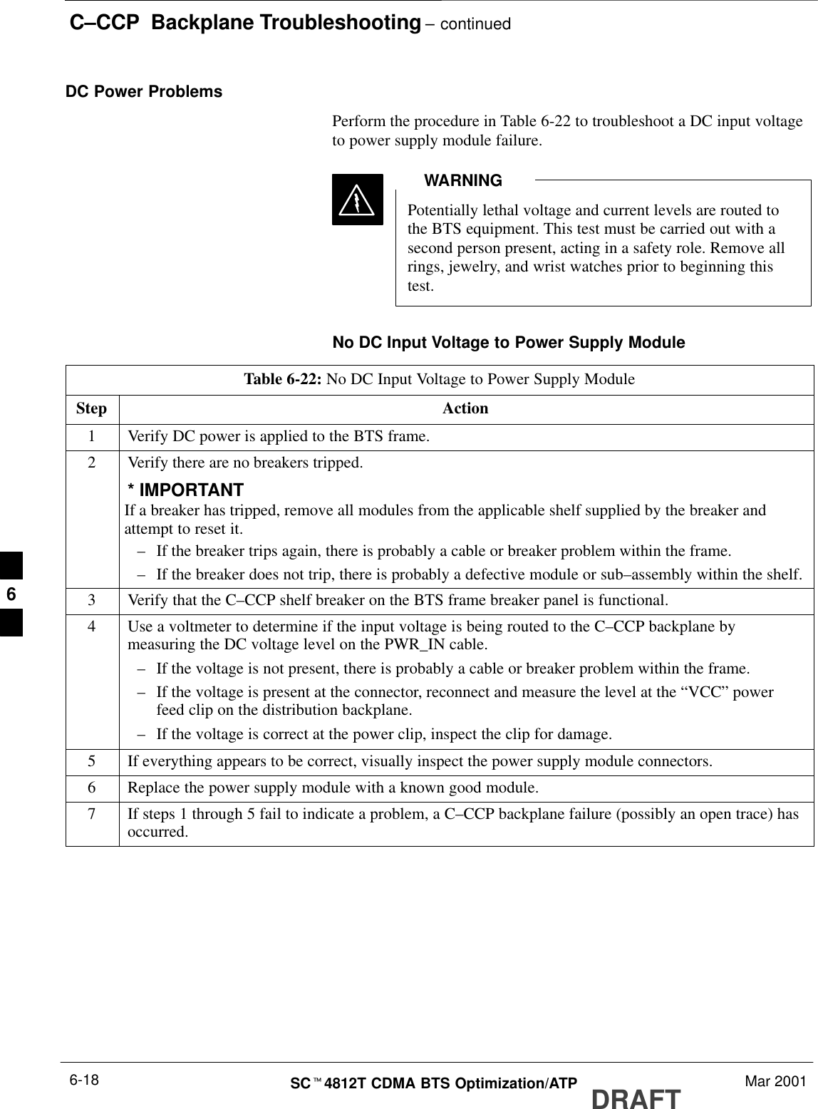
C–CCP  Backplane Troubleshooting – continuedDRAFTSCt4812T CDMA BTS Optimization/ATP Mar 20016-18DC Power ProblemsPerform the procedure in Table 6-22 to troubleshoot a DC input voltageto power supply module failure.Potentially lethal voltage and current levels are routed tothe BTS equipment. This test must be carried out with asecond person present, acting in a safety role. Remove allrings, jewelry, and wrist watches prior to beginning thistest.WARNINGNo DC Input Voltage to Power Supply ModuleTable 6-22: No DC Input Voltage to Power Supply ModuleStep Action1Verify DC power is applied to the BTS frame.2Verify there are no breakers tripped.* IMPORTANTIf a breaker has tripped, remove all modules from the applicable shelf supplied by the breaker andattempt to reset it.–If the breaker trips again, there is probably a cable or breaker problem within the frame.–If the breaker does not trip, there is probably a defective module or sub–assembly within the shelf.3Verify that the C–CCP shelf breaker on the BTS frame breaker panel is functional.4Use a voltmeter to determine if the input voltage is being routed to the C–CCP backplane bymeasuring the DC voltage level on the PWR_IN cable.–If the voltage is not present, there is probably a cable or breaker problem within the frame.–If the voltage is present at the connector, reconnect and measure the level at the “VCC” powerfeed clip on the distribution backplane.–If the voltage is correct at the power clip, inspect the clip for damage.5If everything appears to be correct, visually inspect the power supply module connectors.6Replace the power supply module with a known good module.7If steps 1 through 5 fail to indicate a problem, a C–CCP backplane failure (possibly an open trace) hasoccurred.6
C–CCP Backplane Troubleshooting – continuedMar 2001 6-19SCt4812T CDMA BTS Optimization/ATP DRAFTNo DC Voltage (+5, +6.5, or +15 Volts) to a Specific GLI2,BBX, or SwitchboardPerform the procedure in Table 6-23 to troubleshoot a DC input voltageto GLI2, BBX, or Switchboard failure.Table 6-23: No DC Input Voltage to any C–CCP Shelf ModuleStep Action1Verify the steps in Table 6-22 have been performed.2Inspect the defective board/module (both board and backplane) connector for damage.3Replace suspect board/module with known good board/module.TX and RX Signal RoutingProblemsPerform the procedure in Table 6-24 to troubleshoot TX and RX signalrouting problems.Table 6-24: TX and RX Signal Routing ProblemsStep Action1Inspect all Harting Cable connectors and back–plane connectors for damage in all the affected boardslots.2Perform steps in the RF path troubleshooting flowchart in this manual.6
Module Front Panel LED Indicators and ConnectorsDRAFTSCt4812T CDMA BTS Optimization/ATP Mar 20016-20Module Status IndicatorsEach of the non-passive plug-in modules has a bi-color (green & red)LED status indicator located on the module front panel. The indicator islabeled PWR/ALM. If both colors are turned on, the indicator is yellow.Each plug-in module, except for the fan module, has its own alarm(fault) detection circuitry that controls the state of the PWR/ALM LED.The fan TACH signal of each fan module is monitored by the AMR.Based on the status of this signal, the AMR controls the state of thePWR/ALM LED on the fan module.LED Status Combinations forAll Modules (except GLI2,CSM, BBX, MCC)PWR/ALM LEDThe following list describes the states of the module status indicator.SSolid GREEN –  module operating in a normal (fault free) condition.SSolid RED – module is operating in a fault (alarm) condition due toelectrical hardware failure.Note that a fault (alarm) indication may or may not be due to a completemodule failure and normal service may or may not be reduced orinterrupted.DC/DC Converter LED StatusCombinationsThe PWR CNVTR has alarm (fault) detection circuitry that controls thestate of the PWR/ALM LED. This is true for both the C–CCP and LPApower converters.PWR/ALM LEDThe following list describes the states of the bi-color LED.SSolid GREEN –  module operating in a normal (fault free) condition.SSolid RED –  module is operating in a fault (alarm) condition due toelectrical hardware problem.6
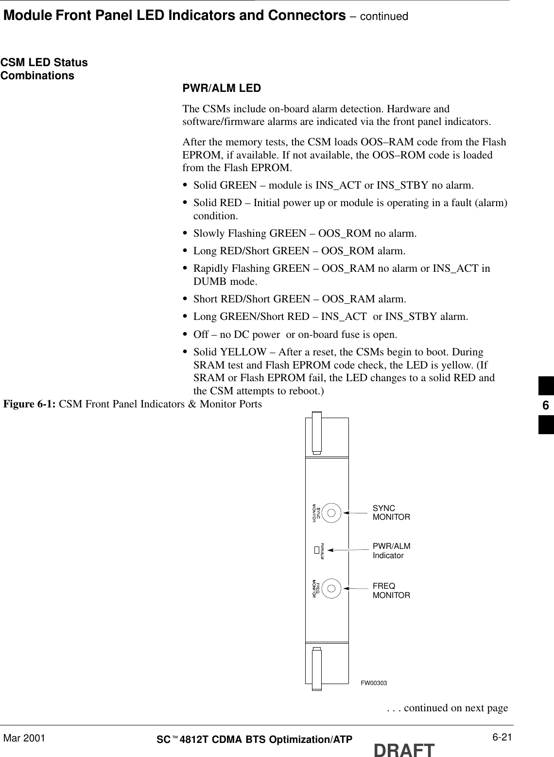
Module Front Panel LED Indicators and Connectors – continuedMar 2001 6-21SCt4812T CDMA BTS Optimization/ATP DRAFTCSM LED StatusCombinations PWR/ALM LEDThe CSMs include on-board alarm detection. Hardware andsoftware/firmware alarms are indicated via the front panel indicators.After the memory tests, the CSM loads OOS–RAM code from the FlashEPROM, if available. If not available, the OOS–ROM code is loadedfrom the Flash EPROM.SSolid GREEN – module is INS_ACT or INS_STBY no alarm.SSolid RED – Initial power up or module is operating in a fault (alarm)condition.SSlowly Flashing GREEN – OOS_ROM no alarm.SLong RED/Short GREEN – OOS_ROM alarm.SRapidly Flashing GREEN – OOS_RAM no alarm or INS_ACT inDUMB mode.SShort RED/Short GREEN – OOS_RAM alarm.SLong GREEN/Short RED – INS_ACT  or INS_STBY alarm.SOff – no DC power  or on-board fuse is open.SSolid YELLOW – After a reset, the CSMs begin to boot. DuringSRAM test and Flash EPROM code check, the LED is yellow. (IfSRAM or Flash EPROM fail, the LED changes to a solid RED andthe CSM attempts to reboot.)PWR/ALMIndicatorFREQMONITORSYNCMONITORFW00303Figure 6-1: CSM Front Panel Indicators & Monitor Ports . . . continued on next page6
Module Front Panel LED Indicators and Connectors – continuedDRAFTSCt4812T CDMA BTS Optimization/ATP Mar 20016-22FREQ Monitor ConnectorA test port provided at the CSM front panel via a BNC receptacle allowsmonitoring of the 19.6608 MHz clock generated by the CSM. Whenboth CSM 1 and CSM 2 are in an in-service (INS) condition, the CSM 2clock signal frequency is the same as that output by CSM 1.The clock is a sine wave signal with a minimum amplitude of +2 dBm(800 mVpp) into a 50 Ω load connected to this port.SYNC Monitor ConnectorA test port provided at the CSM front panel via a BNC receptacle allowsmonitoring of the “Even Second Tick” reference signal generated by theCSMs.At this port, the reference signal is a TTL active high signal with a pulsewidth of 153 nanoseconds.MMI Connector – Only accessible behind front panel. The RS–232MMI port connector is intended to be used primarily in the developmentor factory environment, but may be used in the field fordebug/maintenance purposes.6
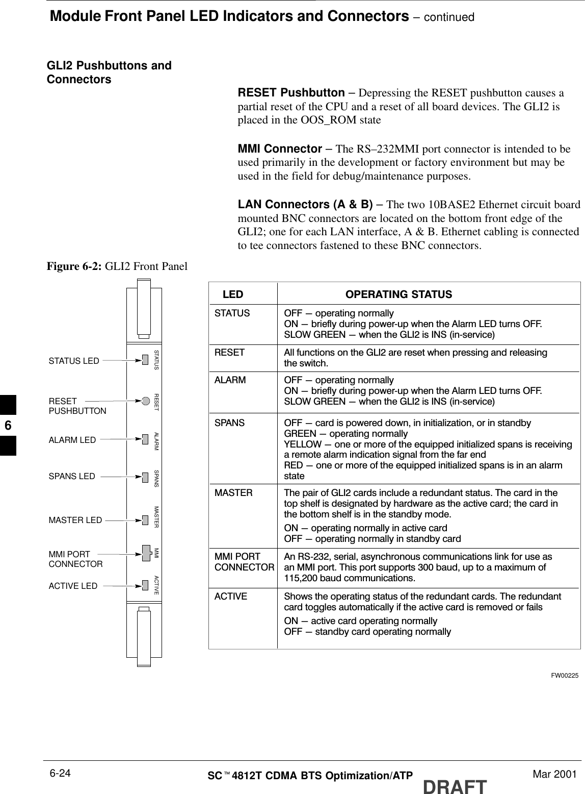
Module Front Panel LED Indicators and Connectors – continuedMar 2001 6-23SCt4812T CDMA BTS Optimization/ATP DRAFTGLI2 LED StatusCombinationsThe GLI2 module has indicators, controls and connectors as describedbelow and shown in Figure 6-2.The operating states of the 5 LEDs are:ACTIVESolid GREEN – GLI2 is active. This means that the GLI2 has shelfcontrol and is providing control of the digital interfaces.Off – GLI2 is not active (i.e., Standby). The mate GLI2 should beactive.MASTERSSolid GREEN – GLI2 is Master (sometimes referred to as MGLI2).SOff – GLI2 is non-master (i.e., Slave).ALARMSSolid RED – GLI2 is in a fault condition or in reset.SWhile in reset transition,  STATUS LED is OFF while GLI2 isperforming ROM boot (about 12 seconds for normal boot).SWhile in reset transition,  STATUS LED is ON while GLI2 isperforming RAM boot (about 4 seconds for normal boot).SOff – No Alarm.STATUSSFlashing GREEN– GLI2 is in service (INS), in a stable operatingcondition.SOn – GLI2 is in OOS RAM state operating downloaded code.SOff – GLI2 is in OOS ROM state operating boot code.SPANSSSolid GREEN – Span line is connected and operating.SSolid RED – Span line is disconnected or a fault condition exists.6
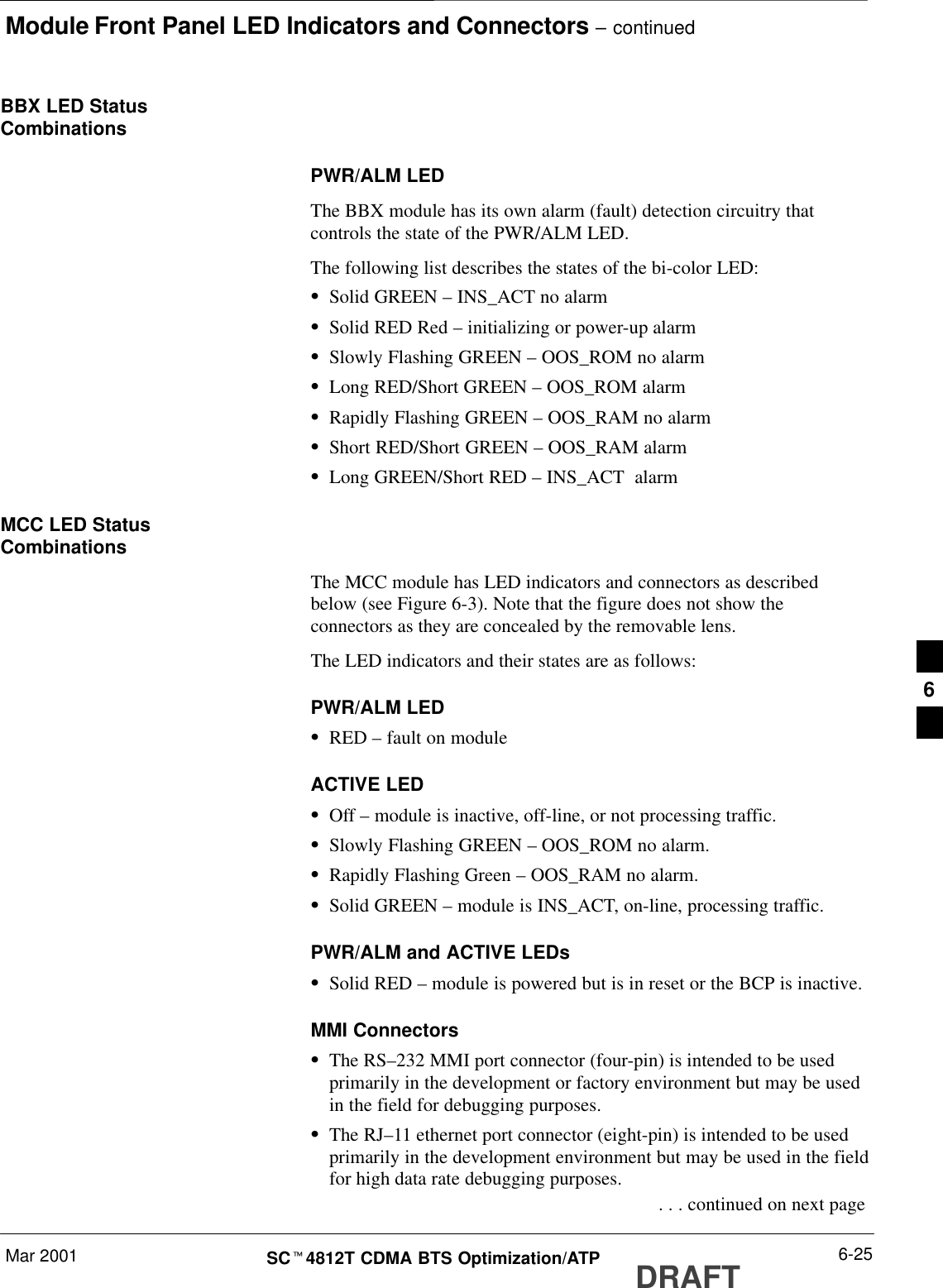
Module Front Panel LED Indicators and Connectors – continuedDRAFTSCt4812T CDMA BTS Optimization/ATP Mar 20016-24GLI2 Pushbuttons andConnectors RESET Pushbutton – Depressing the RESET pushbutton causes apartial reset of the CPU and a reset of all board devices. The GLI2 isplaced in the OOS_ROM stateMMI Connector – The RS–232MMI port connector is intended to beused primarily in the development or factory environment but may beused in the field for debug/maintenance purposes.LAN Connectors (A & B) – The two 10BASE2 Ethernet circuit boardmounted BNC connectors are located on the bottom front edge of theGLI2; one for each LAN interface, A & B. Ethernet cabling is connectedto tee connectors fastened to these BNC connectors.Figure 6-2: GLI2 Front PanelMMI PORTCONNECTORACTIVE LEDSTATUS RESET ALARM SPANS MASTER MMI ACTIVESTATUS LEDRESETPUSHBUTTONALARM LEDSPANS LEDMASTER LEDSTATUS OFF - operating normallyON - briefly during powerĆup when the Alarm LED turns OFF.SLOW GREEN - when the GLI2 is INS (inĆservice)RESETALARM OFF - operating normallyON - briefly during powerĆup when the Alarm LED turns OFF.SLOW GREEN - when the GLI2 is INS (inĆservice)SPANSMASTERMMI PORTCONNECTORACTIVELED OPERATING STATUSAll functions on the GLI2 are reset when pressing and releasingthe switch.ON - operating normally in active cardOFF - operating normally in standby cardShows the operating status of the redundant cards. The redundantcard toggles automatically if the active card is removed or failsON - active card operating normallyOFF - standby card operating normallyThe pair of GLI2 cards include a redundant status. The card in thetop shelf is designated by hardware as the active card; the card inthe bottom shelf is in the standby mode.OFF - card is powered down, in initialization, or in standbyGREEN - operating normallyYELLOW - one or more of the equipped initialized spans is receivinga remote alarm indication signal from the far endRED - one or more of the equipped initialized spans is in an alarmstateAn RSĆ232, serial, asynchronous communications link for use asan MMI port. This port supports 300 baud, up to a maximum of115,200 baud communications.FW002256
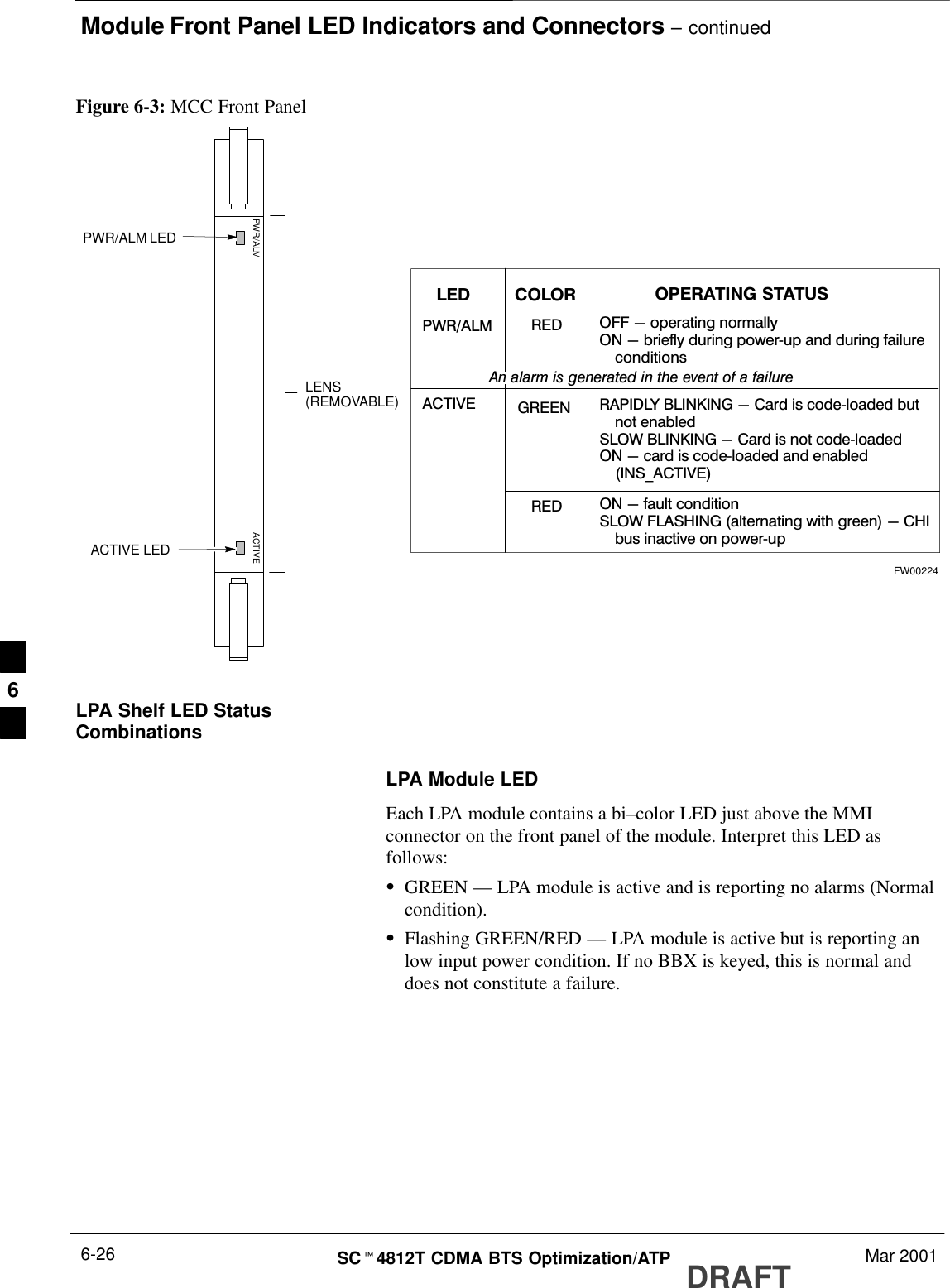
Module Front Panel LED Indicators and Connectors – continuedMar 2001 6-25SCt4812T CDMA BTS Optimization/ATP DRAFTBBX LED StatusCombinationsPWR/ALM LEDThe BBX module has its own alarm (fault) detection circuitry thatcontrols the state of the PWR/ALM LED.The following list describes the states of the bi-color LED:SSolid GREEN – INS_ACT no alarmSSolid RED Red – initializing or power-up alarmSSlowly Flashing GREEN – OOS_ROM no alarmSLong RED/Short GREEN – OOS_ROM alarmSRapidly Flashing GREEN – OOS_RAM no alarmSShort RED/Short GREEN – OOS_RAM alarmSLong GREEN/Short RED – INS_ACT  alarmMCC LED StatusCombinationsThe MCC module has LED indicators and connectors as describedbelow (see Figure 6-3). Note that the figure does not show theconnectors as they are concealed by the removable lens.The LED indicators and their states are as follows:PWR/ALM LEDSRED – fault on moduleACTIVE LEDSOff – module is inactive, off-line, or not processing traffic.SSlowly Flashing GREEN – OOS_ROM no alarm.SRapidly Flashing Green – OOS_RAM no alarm.SSolid GREEN – module is INS_ACT, on-line, processing traffic.PWR/ALM and ACTIVE LEDsSSolid RED – module is powered but is in reset or the BCP is inactive.MMI ConnectorsSThe RS–232 MMI port connector (four-pin) is intended to be usedprimarily in the development or factory environment but may be usedin the field for debugging purposes.SThe RJ–11 ethernet port connector (eight-pin) is intended to be usedprimarily in the development environment but may be used in the fieldfor high data rate debugging purposes. . . . continued on next page6
Module Front Panel LED Indicators and Connectors – continuedDRAFTSCt4812T CDMA BTS Optimization/ATP Mar 20016-26Figure 6-3: MCC Front PanelPWR/ALM LEDLENS(REMOVABLE)ACTIVE LEDPWR/ALM ACTIVEPWR/ALM OFF - operating normallyON - briefly during powerĆup and during failureąconditionsACTIVELED OPERATING STATUSRAPIDLY BLINKING -  Card is  codeĆloaded butąnot enabledSLOW BLINKING - Card is not codeĆloadedON - card is codeĆloaded and enabledą(INS_ACTIVE)COLORGREENREDRED ON - fault conditionSLOW FLASHING (alternating with green) - CHIąbus inactive on powerĆupAn alarm is generated in the event of a failureFW00224LPA Shelf LED StatusCombinationsLPA Module LEDEach LPA module contains a bi–color LED just above the MMIconnector on the front panel of the module. Interpret this LED asfollows:SGREEN — LPA module is active and is reporting no alarms (Normalcondition).SFlashing GREEN/RED — LPA module is active but is reporting anlow input power condition. If no BBX is keyed, this is normal anddoes not constitute a failure.6
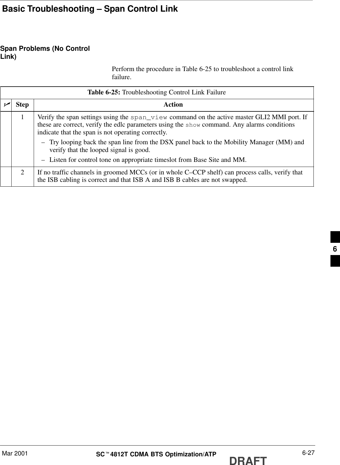
Basic Troubleshooting – Span Control LinkMar 2001 6-27SCt4812T CDMA BTS Optimization/ATP DRAFTSpan Problems (No ControlLink)Perform the procedure in Table 6-25 to troubleshoot a control linkfailure.Table 6-25: Troubleshooting Control Link FailurenStep Action1Verify the span settings using the span_view command on the active master GLI2 MMI port. Ifthese are correct, verify the edlc parameters using the show command. Any alarms conditionsindicate that the span is not operating correctly.–Try looping back the span line from the DSX panel back to the Mobility Manager (MM) andverify that the looped signal is good.–Listen for control tone on appropriate timeslot from Base Site and MM.2If no traffic channels in groomed MCCs (or in whole C–CCP shelf) can process calls, verify thatthe ISB cabling is correct and that ISB A and ISB B cables are not swapped.6
Basic Troubleshooting – Span Control Link – continuedDRAFTSCt4812T CDMA BTS Optimization/ATP Mar 20016-28Notes6
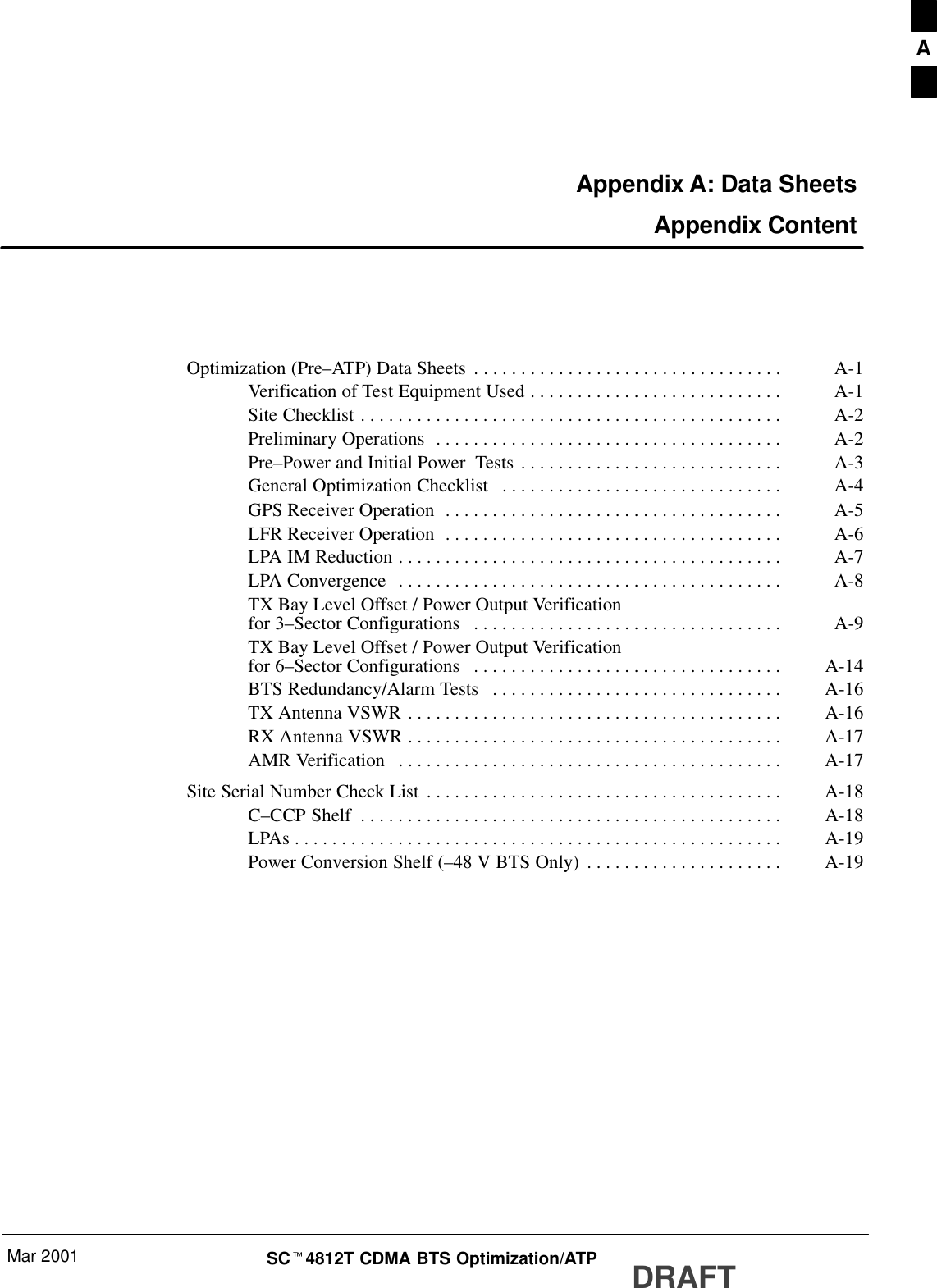
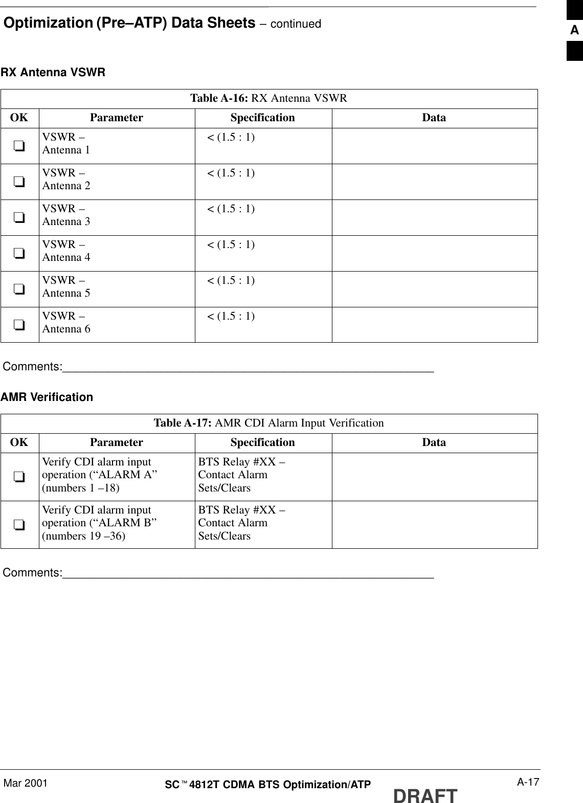
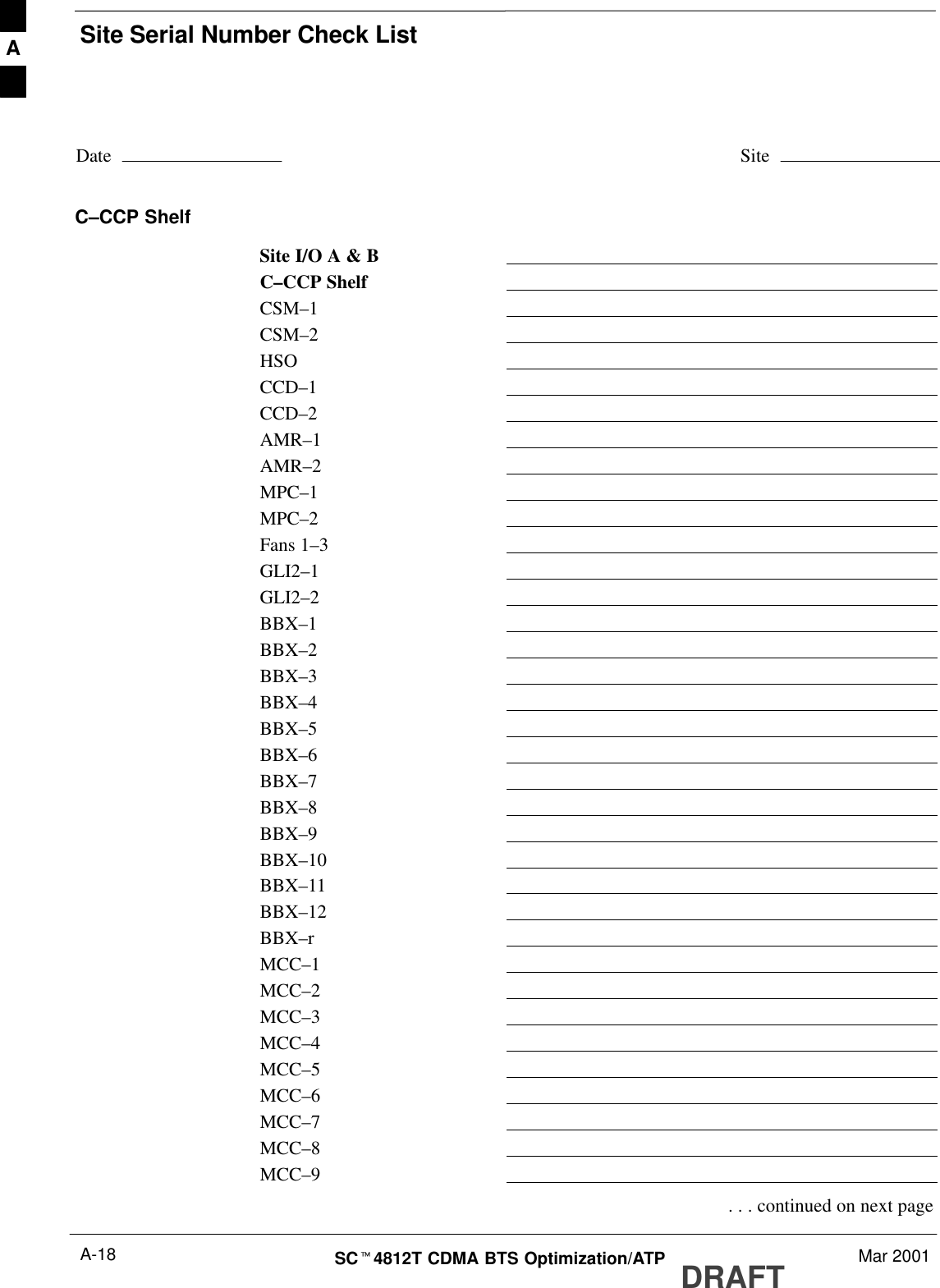
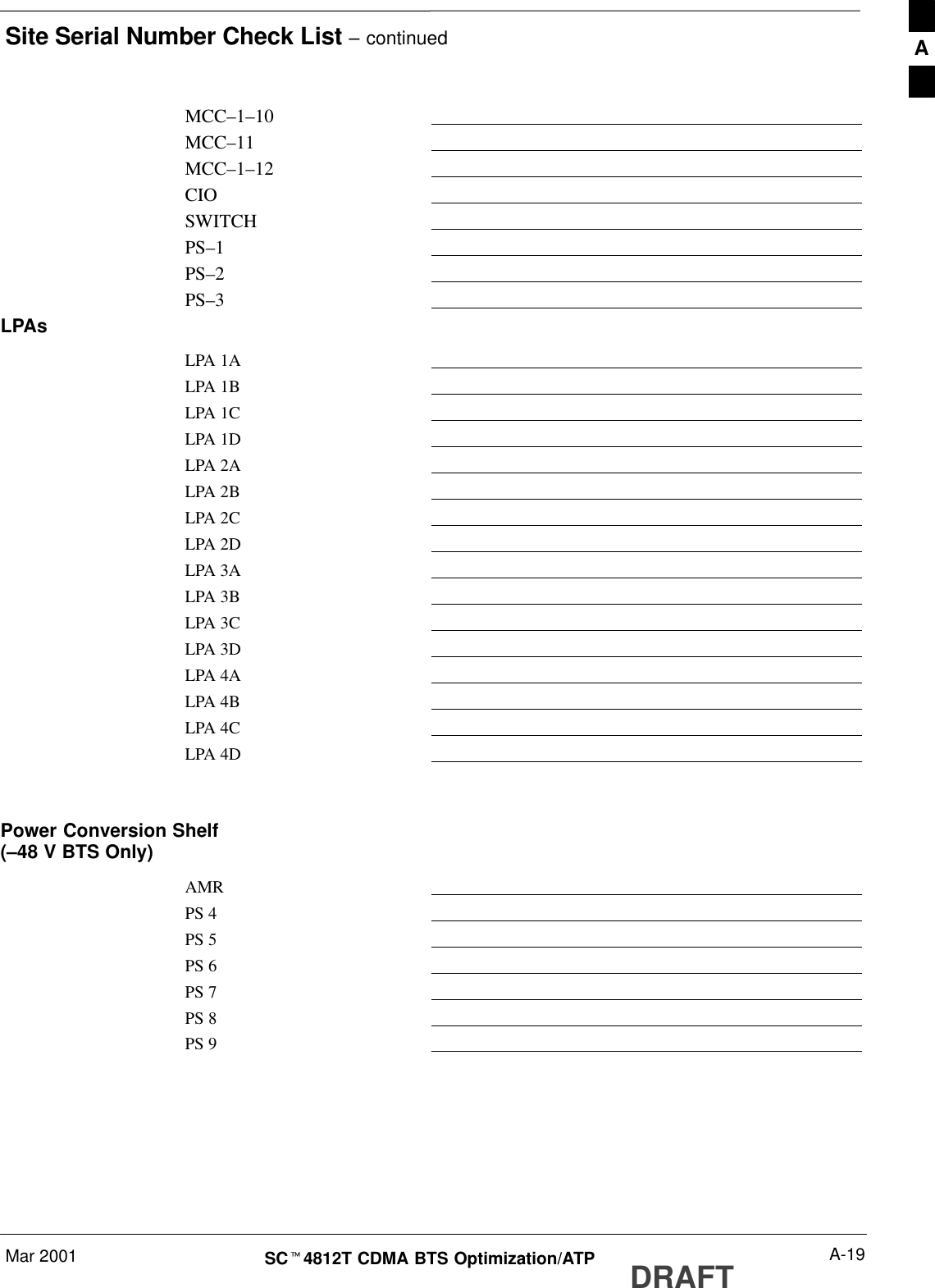
Mar 2001 SCt4812T CDMA BTS Optimization/ATP DRAFTAppendix A: Data Sheets Appendix ContentOptimization (Pre–ATP) Data Sheets A-1. . . . . . . . . . . . . . . . . . . . . . . . . . . . . . . . . Verification of Test Equipment Used A-1. . . . . . . . . . . . . . . . . . . . . . . . . . . Site Checklist A-2. . . . . . . . . . . . . . . . . . . . . . . . . . . . . . . . . . . . . . . . . . . . . Preliminary Operations A-2. . . . . . . . . . . . . . . . . . . . . . . . . . . . . . . . . . . . . Pre–Power and Initial Power  Tests A-3. . . . . . . . . . . . . . . . . . . . . . . . . . . . General Optimization Checklist A-4. . . . . . . . . . . . . . . . . . . . . . . . . . . . . . GPS Receiver Operation A-5. . . . . . . . . . . . . . . . . . . . . . . . . . . . . . . . . . . . LFR Receiver Operation A-6. . . . . . . . . . . . . . . . . . . . . . . . . . . . . . . . . . . . LPA IM Reduction A-7. . . . . . . . . . . . . . . . . . . . . . . . . . . . . . . . . . . . . . . . . LPA Convergence A-8. . . . . . . . . . . . . . . . . . . . . . . . . . . . . . . . . . . . . . . . . TX Bay Level Offset / Power Output Verificationfor 3–Sector Configurations A-9. . . . . . . . . . . . . . . . . . . . . . . . . . . . . . . . . TX Bay Level Offset / Power Output Verificationfor 6–Sector Configurations A-14. . . . . . . . . . . . . . . . . . . . . . . . . . . . . . . . . BTS Redundancy/Alarm Tests A-16. . . . . . . . . . . . . . . . . . . . . . . . . . . . . . . TX Antenna VSWR A-16. . . . . . . . . . . . . . . . . . . . . . . . . . . . . . . . . . . . . . . . RX Antenna VSWR A-17. . . . . . . . . . . . . . . . . . . . . . . . . . . . . . . . . . . . . . . . AMR Verification A-17. . . . . . . . . . . . . . . . . . . . . . . . . . . . . . . . . . . . . . . . . Site Serial Number Check List A-18. . . . . . . . . . . . . . . . . . . . . . . . . . . . . . . . . . . . . . C–CCP Shelf A-18. . . . . . . . . . . . . . . . . . . . . . . . . . . . . . . . . . . . . . . . . . . . . LPAs A-19. . . . . . . . . . . . . . . . . . . . . . . . . . . . . . . . . . . . . . . . . . . . . . . . . . . . Power Conversion Shelf (–48 V BTS Only) A-19. . . . . . . . . . . . . . . . . . . . . A
Table of Contents  – continuedDRAFTSCt4812T CDMA BTS Optimization/ATP Mar 2001NotesA
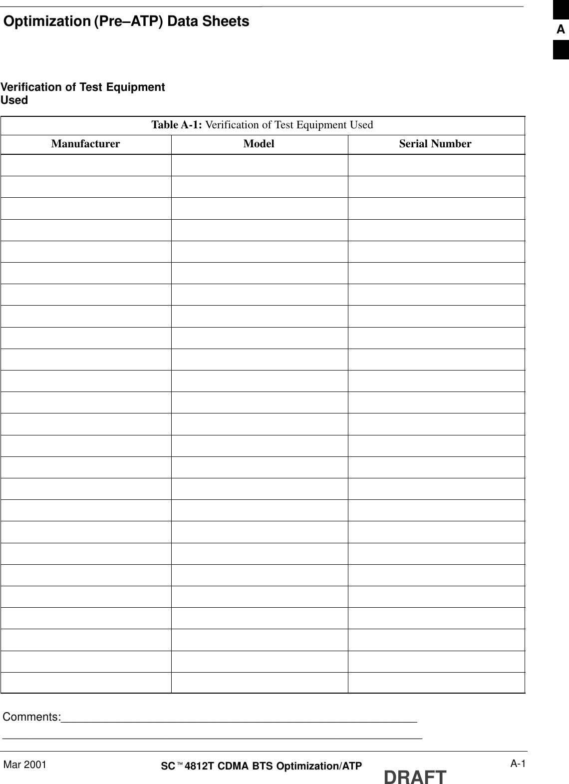
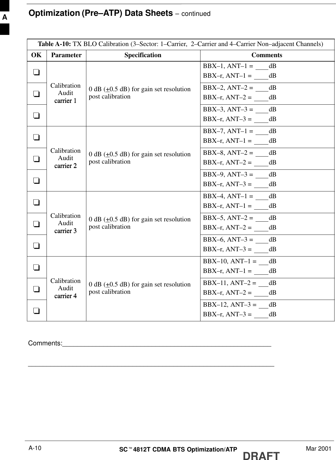
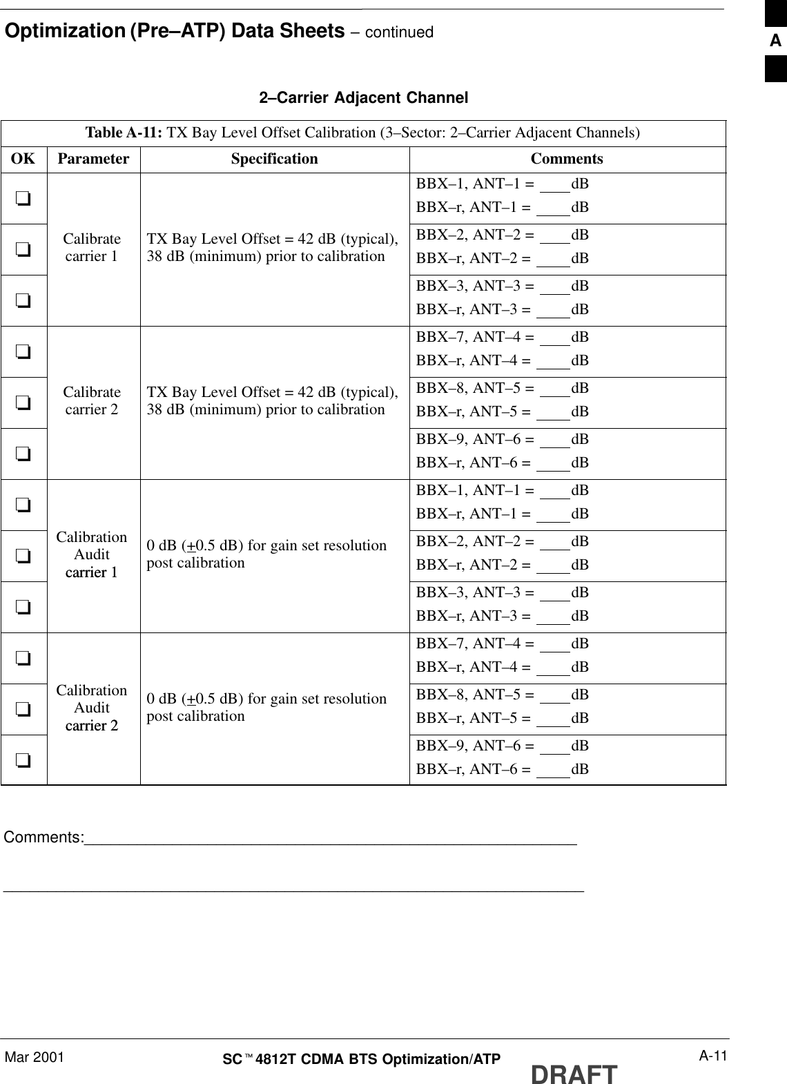
Optimization (Pre–ATP) Data SheetsMar 2001 A-1SCt4812T CDMA BTS Optimization/ATP DRAFTVerification of Test EquipmentUsedTable A-1: Verification of Test Equipment UsedManufacturer Model Serial NumberComments:__________________________________________________________________________________________________________________________A
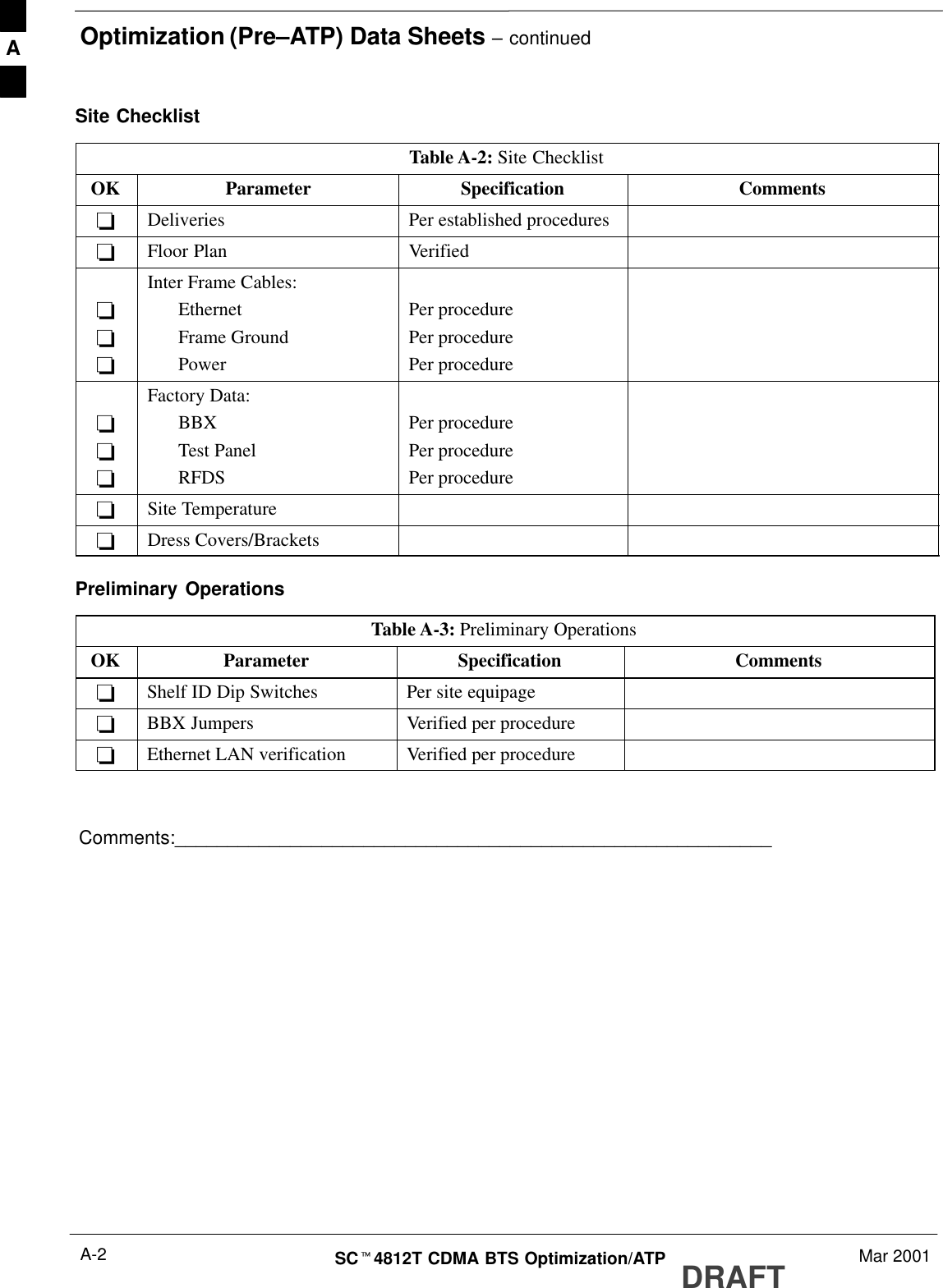
Optimization (Pre–ATP) Data Sheets – continuedDRAFTSCt4812T CDMA BTS Optimization/ATP Mar 2001A-2Site ChecklistTable A-2: Site ChecklistOK Parameter Specification Comments-Deliveries Per established procedures-Floor Plan Verified---Inter Frame Cables:EthernetFrame GroundPowerPer procedurePer procedurePer procedure---Factory Data:BBXTest PanelRFDSPer procedurePer procedurePer procedure-Site Temperature-Dress Covers/BracketsPreliminary OperationsTable A-3: Preliminary OperationsOK Parameter Specification Comments-Shelf ID Dip Switches Per site equipage-BBX Jumpers Verified per procedure-Ethernet LAN verification Verified per procedureComments:_________________________________________________________A
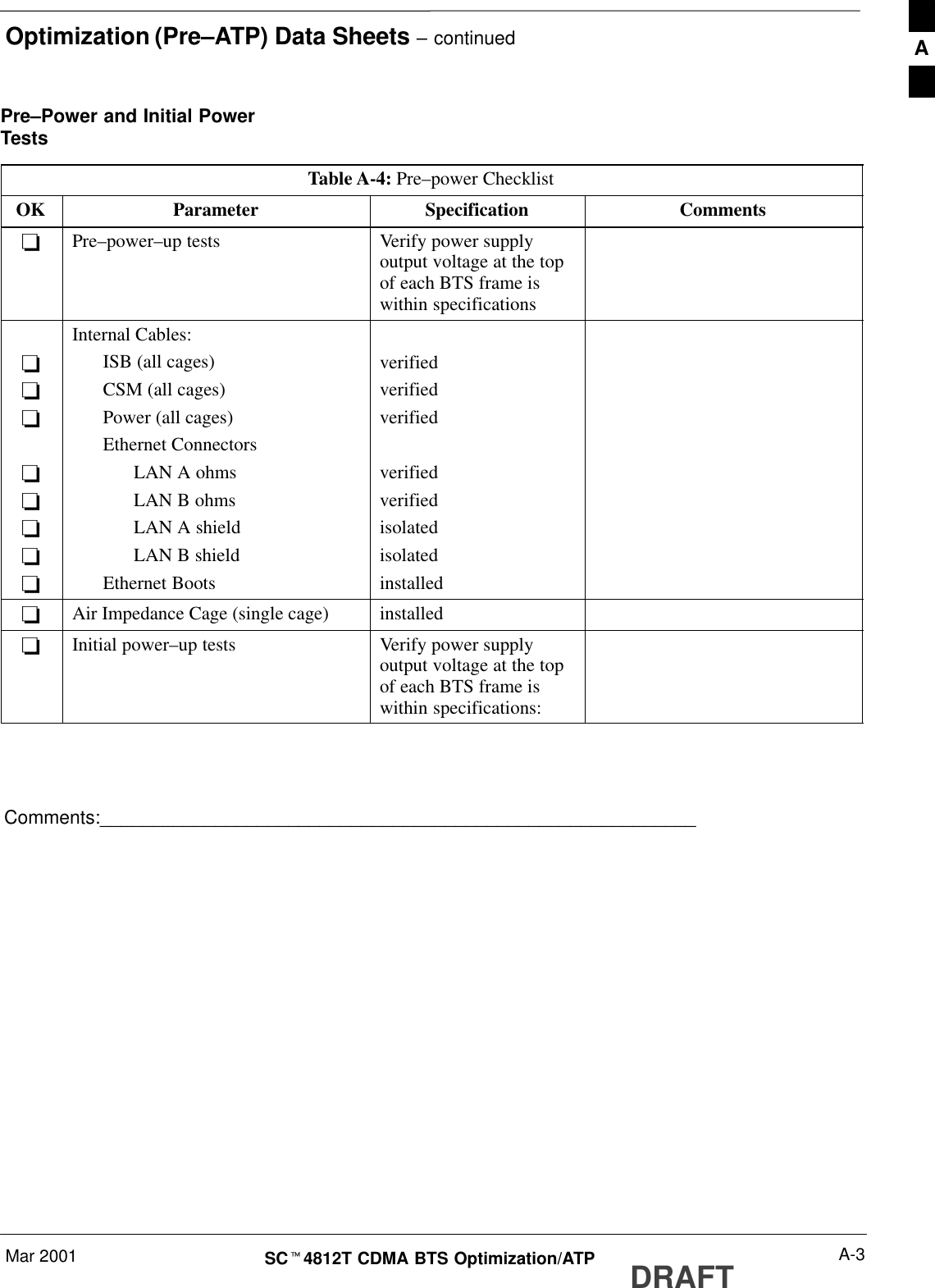
Optimization (Pre–ATP) Data Sheets – continuedMar 2001 A-3SCt4812T CDMA BTS Optimization/ATP DRAFTPre–Power and Initial PowerTestsTable A-4: Pre–power ChecklistOK Parameter Specification Comments-Pre–power–up tests Verify power supplyoutput voltage at the topof each BTS frame iswithin specifications--------Internal Cables:ISB (all cages)CSM (all cages)Power (all cages)Ethernet ConnectorsLAN A ohmsLAN B ohmsLAN A shieldLAN B shieldEthernet Bootsverifiedverifiedverifiedverifiedverifiedisolatedisolatedinstalled-Air Impedance Cage (single cage) installed-Initial power–up tests Verify power supplyoutput voltage at the topof each BTS frame iswithin specifications:Comments:_________________________________________________________A
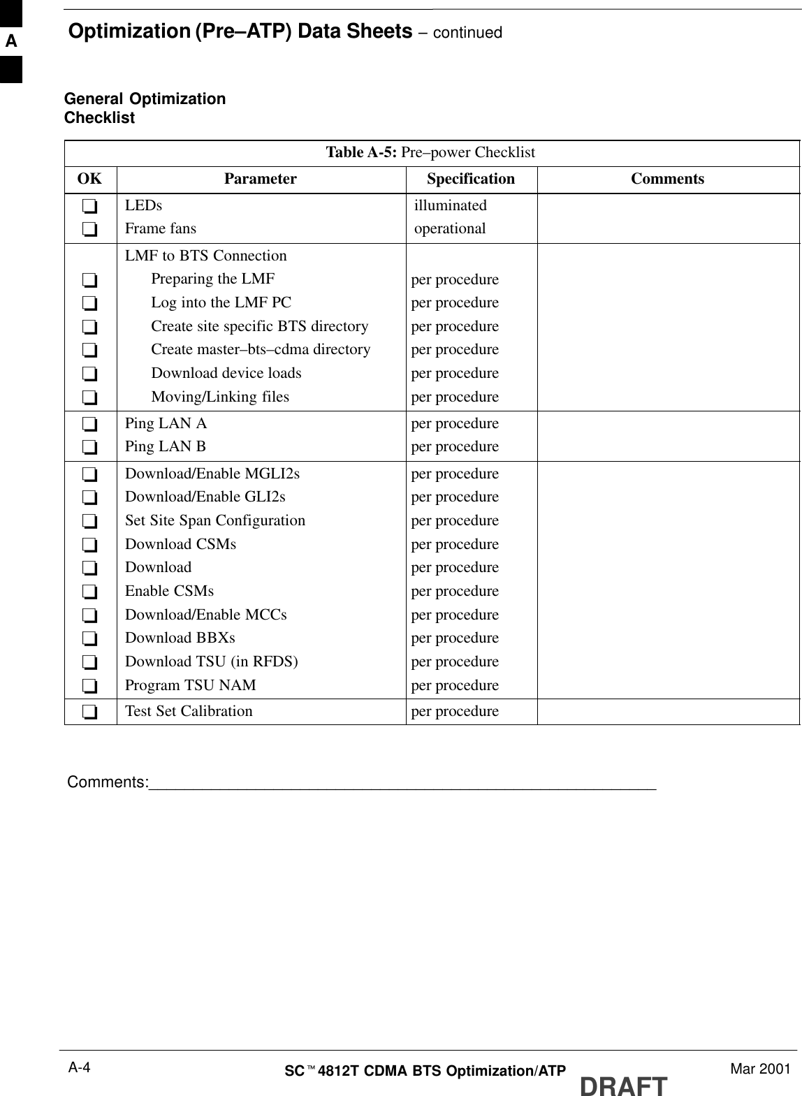
Optimization (Pre–ATP) Data Sheets – continuedDRAFTSCt4812T CDMA BTS Optimization/ATP Mar 2001A-4General OptimizationChecklistTable A-5: Pre–power ChecklistOK Parameter Specification Comments--LEDsFrame fansilluminatedoperational------LMF to BTS ConnectionPreparing the LMFLog into the LMF PCCreate site specific BTS directoryCreate master–bts–cdma directoryDownload device loadsMoving/Linking filesper procedureper procedureper procedureper procedureper procedureper procedure--Ping LAN APing LAN Bper procedureper procedure----------Download/Enable MGLI2sDownload/Enable GLI2sSet Site Span ConfigurationDownload CSMsDownloadEnable CSMsDownload/Enable MCCsDownload BBXsDownload TSU (in RFDS)Program TSU NAMper procedureper procedureper procedureper procedureper procedureper procedureper procedureper procedureper procedureper procedure-Test Set Calibration per procedureComments:_________________________________________________________A
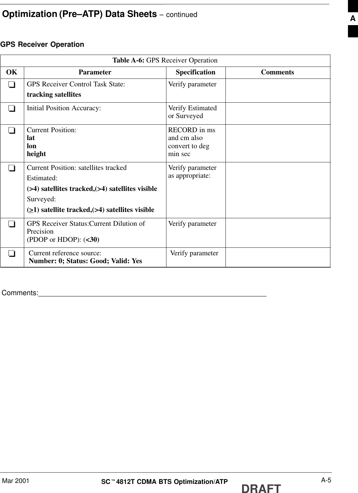
Optimization (Pre–ATP) Data Sheets – continuedMar 2001 A-5SCt4812T CDMA BTS Optimization/ATP DRAFTGPS Receiver OperationTable A-6: GPS Receiver OperationOK Parameter Specification Comments-GPS Receiver Control Task State:tracking satellitesVerify parameter-Initial Position Accuracy: Verify Estimatedor Surveyed-Current Position:latlonheightRECORD in msand cm alsoconvert to degmin sec-Current Position: satellites trackedEstimated:(>4) satellites tracked,(>4) satellites visibleSurveyed:(>1) satellite tracked,(>4) satellites visibleVerify parameteras appropriate:-GPS Receiver Status:Current Dilution ofPrecision (PDOP or HDOP): (<30)Verify parameter-Current reference source:Number: 0; Status: Good; Valid: Yes Verify parameterComments:_________________________________________________________A
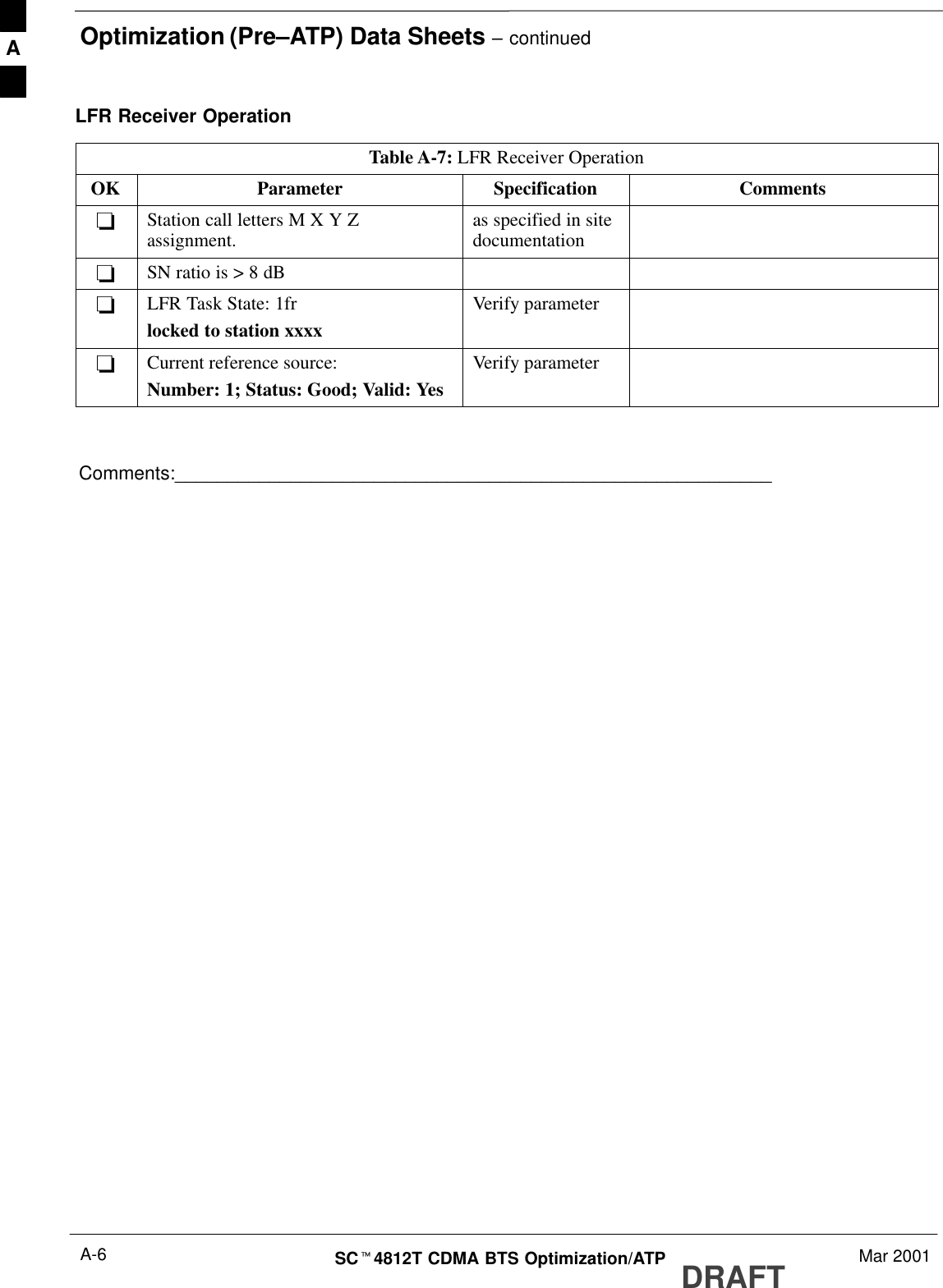
Optimization (Pre–ATP) Data Sheets – continuedDRAFTSCt4812T CDMA BTS Optimization/ATP Mar 2001A-6LFR Receiver OperationTable A-7: LFR Receiver OperationOK Parameter Specification Comments-Station call letters M X Y Zassignment. as specified in sitedocumentation-SN ratio is > 8 dB-LFR Task State: 1frlocked to station xxxxVerify parameter-Current reference source:Number: 1; Status: Good; Valid: YesVerify parameterComments:_________________________________________________________A
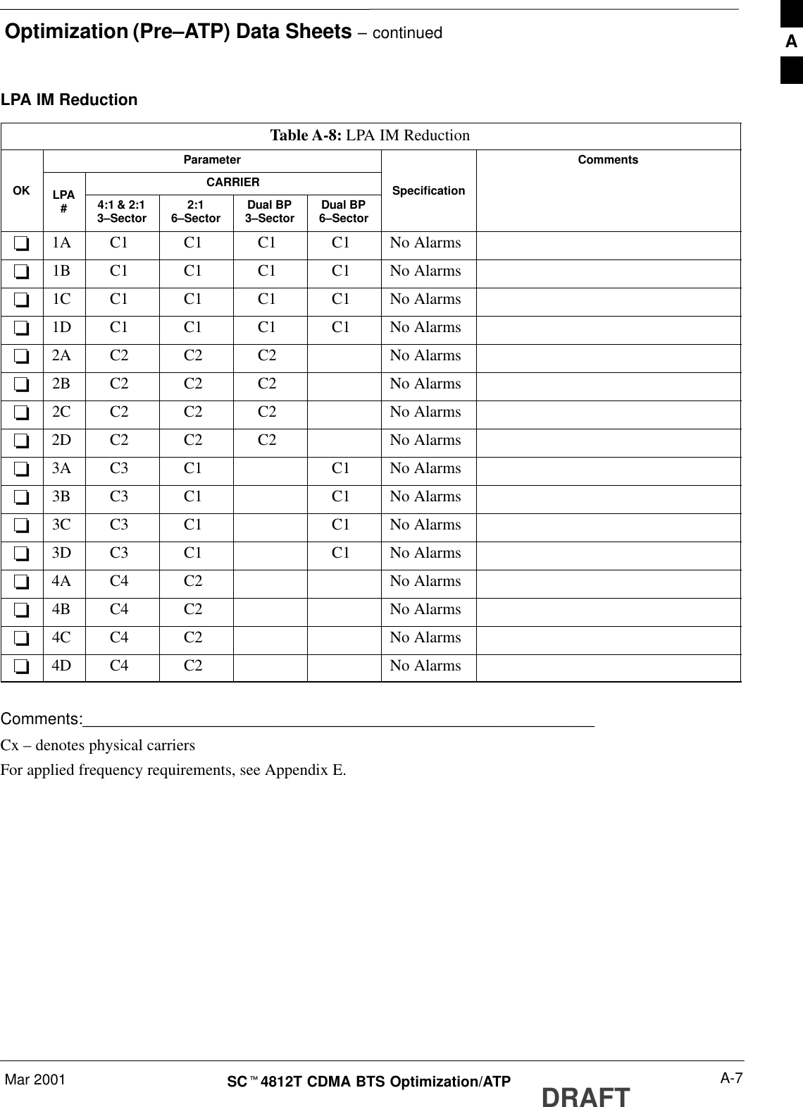
Optimization (Pre–ATP) Data Sheets – continuedMar 2001 A-7SCt4812T CDMA BTS Optimization/ATP DRAFTLPA IM ReductionTable A-8: LPA IM ReductionParameter CommentsCARRIEROK LPA#4:1 & 2:13–Sector 2:16–Sector Dual BP3–Sector Dual BP6–SectorSpecification-1A C1 C1 C1 C1 No Alarms-1B C1 C1 C1 C1 No Alarms-1C C1 C1 C1 C1 No Alarms-1D C1 C1 C1 C1 No Alarms-2A C2 C2 C2 No Alarms-2B C2 C2 C2 No Alarms-2C C2 C2 C2 No Alarms-2D C2 C2 C2 No Alarms-3A C3 C1 C1 No Alarms-3B C3 C1 C1 No Alarms-3C C3 C1 C1 No Alarms-3D C3 C1 C1 No Alarms-4A C4 C2 No Alarms-4B C4 C2 No Alarms-4C C4 C2 No Alarms-4D C4 C2 No AlarmsComments:_________________________________________________________Cx – denotes physical carriersFor applied frequency requirements, see Appendix E.A
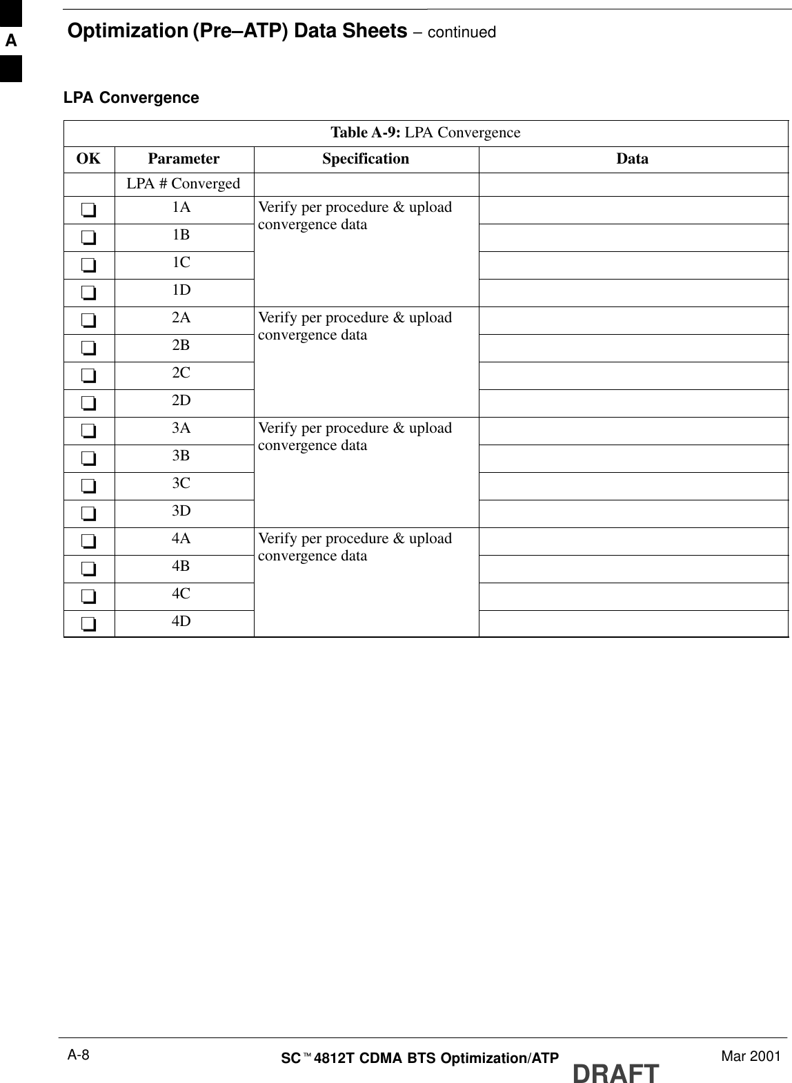
Optimization (Pre–ATP) Data Sheets – continuedDRAFTSCt4812T CDMA BTS Optimization/ATP Mar 2001A-8LPA ConvergenceTable A-9: LPA ConvergenceOK Parameter Specification DataLPA # Converged-1A Verify per procedure & upload-1B convergence data-1C-1D-2A Verify per procedure & upload-2B convergence data-2C-2D-3A Verify per procedure & upload-3B convergence data-3C-3D-4A Verify per procedure & upload-4B convergence data-4C-4DA
Optimization (Pre–ATP) Data Sheets – continuedMar 2001 A-9SCt4812T CDMA BTS Optimization/ATP DRAFTTX Bay Level Offset/PowerOutput Verification for3–Sector Configurations 1–Carrier2–Carrier Non–adjacent Channels4–Carrier Non–adjacent ChannelsTable A-10: TX BLO Calibration (3–Sector: 1–Carrier,  2–Carrier and 4–Carrier Non–adjacent Channels)OK Parameter Specification Comments-BBX–1, ANT–1 =  dBBBX–r, ANT–1 =  dB-Calibratecarrier 1 TX Bay Level Offset = 42 dB (+4 dB)prior to calibrationBBX–2, ANT–2 =  dBBBX–r, ANT–2 =  dB-BBX–3, ANT–3 =  dBBBX–r, ANT–3 =  dB-BBX–7, ANT–1 =  dBBBX–r, ANT–1 =  dB-Calibratecarrier 2 TX Bay Level Offset = 42 dB (+4 dB)prior to calibrationBBX–8, ANT–2 =  dBBBX–r, ANT–2 =  dB-BBX–9, ANT–3 =  dBBBX–r, ANT–3 =  dB-BBX–4, ANT–1 =  dBBBX–r, ANT–1 =  dB-Calibratecarrier 3 TX Bay Level Offset = 42 dB (+4 dB)prior to calibrationBBX–5, ANT–2 =  dBBBX–r, ANT–2 =  dB-BBX–6, ANT–3 =  dBBBX–r, ANT–3 =  dB-BBX–10, ANT–1 =  dBBBX–r, ANT–1 =  dB-Calibratecarrier 4 TX Bay Level Offset = 42 dB (+4 dB)prior to calibrationBBX–11, ANT–2 =  dBBBX–r, ANT–2 =  dB-BBX–12, ANT–3 =  dBBBX–r, ANT–3 =  dB. . . continued on next pageA
Optimization (Pre–ATP) Data Sheets – continuedDRAFTSCt4812T CDMA BTS Optimization/ATP Mar 2001A-10Table A-10: TX BLO Calibration (3–Sector: 1–Carrier,  2–Carrier and 4–Carrier Non–adjacent Channels)OK CommentsSpecificationParameter-BBX–1, ANT–1 =  dBBBX–r, ANT–1 =  dB-CalibrationAuditcarrier 10 dB (+0.5 dB) for gain set resolutionpost calibrationBBX–2, ANT–2 =  dBBBX–r, ANT–2 =  dB-carrier 1BBX–3, ANT–3 =  dBBBX–r, ANT–3 =  dB-BBX–7, ANT–1 =  dBBBX–r, ANT–1 =  dB-CalibrationAuditcarrier 20 dB (+0.5 dB) for gain set resolutionpost calibrationBBX–8, ANT–2 =  dBBBX–r, ANT–2 =  dB-carrier 2BBX–9, ANT–3 =  dBBBX–r, ANT–3 =  dB-BBX–4, ANT–1 =  dBBBX–r, ANT–1 =  dB-CalibrationAuditcarrier 30 dB (+0.5 dB) for gain set resolutionpost calibrationBBX–5, ANT–2 =  dBBBX–r, ANT–2 =  dB-carrier 3BBX–6, ANT–3 =  dBBBX–r, ANT–3 =  dB-BBX–10, ANT–1 =  dBBBX–r, ANT–1 =  dB-CalibrationAuditcarrier 40 dB (+0.5 dB) for gain set resolutionpost calibrationBBX–11, ANT–2 =  dBBBX–r, ANT–2 =  dB-carrier 4BBX–12, ANT–3 =  dBBBX–r, ANT–3 =  dB Comments:__________________________________________________________________________________________________________________________A
Optimization (Pre–ATP) Data Sheets – continuedMar 2001 A-11SCt4812T CDMA BTS Optimization/ATP DRAFT2–Carrier Adjacent ChannelTable A-11: TX Bay Level Offset Calibration (3–Sector: 2–Carrier Adjacent Channels)OK Parameter Specification Comments-BBX–1, ANT–1 =  dBBBX–r, ANT–1 =  dB-Calibratecarrier 1 TX Bay Level Offset = 42 dB (typical),38 dB (minimum) prior to calibrationBBX–2, ANT–2 =  dBBBX–r, ANT–2 =  dB-BBX–3, ANT–3 =  dBBBX–r, ANT–3 =  dB-BBX–7, ANT–4 =  dBBBX–r, ANT–4 =  dB-Calibratecarrier 2 TX Bay Level Offset = 42 dB (typical),38 dB (minimum) prior to calibrationBBX–8, ANT–5 =  dBBBX–r, ANT–5 =  dB-BBX–9, ANT–6 =  dBBBX–r, ANT–6 =  dB-BBX–1, ANT–1 =  dBBBX–r, ANT–1 =  dB-CalibrationAuditcarrier 10 dB (+0.5 dB) for gain set resolutionpost calibrationBBX–2, ANT–2 =  dBBBX–r, ANT–2 =  dB-carrier 1BBX–3, ANT–3 =  dBBBX–r, ANT–3 =  dB-BBX–7, ANT–4 =  dBBBX–r, ANT–4 =  dB-CalibrationAuditcarrier 20 dB (+0.5 dB) for gain set resolutionpost calibrationBBX–8, ANT–5 =  dBBBX–r, ANT–5 =  dB-carrier 2BBX–9, ANT–6 =  dBBBX–r, ANT–6 =  dB Comments:__________________________________________________________________________________________________________________________A
Optimization (Pre–ATP) Data Sheets – continuedDRAFTSCt4812T CDMA BTS Optimization/ATP Mar 2001A-123–Carrier Adjacent Channels4–Carrier Adjacent ChannelsTable A-12: TX Bay Level Offset Calibration (3–Sector: 3 or 4–Carrier Adjacent Channels)OK Parameter Specification Comments-BBX–1, ANT–1 =  dBBBX–r, ANT–1 =  dB-Calibratecarrier 1 TX Bay Level Offset = 42 dB (+4 dB)prior to calibrationBBX–2, ANT–2 =  dBBBX–r, ANT–2 =  dB-BBX–3, ANT–3 =  dBBBX–r, ANT–3 =  dB-BBX–7, ANT–1 =  dBBBX–r, ANT–1 =  dB-Calibratecarrier 2 TX Bay Level Offset = 42 dB (+4 dB)prior to calibrationBBX–8, ANT–2 =  dBBBX–r, ANT–2 =  dB-BBX–9, ANT–3 =  dBBBX–r, ANT–3 =  dB-BBX–4, ANT–4 =  dBBBX–r, ANT–4 =  dB-Calibratecarrier 3 TX Bay Level Offset = 42 dB (+4 dB)prior to calibrationBBX–5, ANT–5 =  dBBBX–r, ANT–5 =  dB-BBX–6, ANT–6 =  dBBBX–r, ANT–6 =  dB-BBX–10, ANT–4 =  dBBBX–3, ANT–4 =  dB-Calibratecarrier 4 TX Bay Level Offset = 42 dB (+4 dB)prior to calibrationBBX–11, ANT–5 =  dBBBX–r, ANT–5 =  dB-BBX–12, ANT–6 =  dBBBX–r, ANT–6 =  dB-BBX–1, ANT–1 =  dBBBX–r, ANT–1 =  dB-CalibrationAuditcarrier 10 dB (+0.5 dB) for gain set resolutionpost calibrationBBX–2, ANT–2 =  dBBBX–r, ANT–2 =  dB-carrier 1BBX–3, ANT–3 =  dBBBX–r, ANT–3 =  dB. . . continued on next pageA
Optimization (Pre–ATP) Data Sheets – continuedMar 2001 A-13SCt4812T CDMA BTS Optimization/ATP DRAFTTable A-12: TX Bay Level Offset Calibration (3–Sector: 3 or 4–Carrier Adjacent Channels)OK CommentsSpecificationParameter-BBX–7, ANT–1 =  dBBBX–r, ANT–1 =  dB-CalibrationAuditcarrier 20 dB (+0.5 dB) for gain set resolutionpost calibrationBBX–8, ANT–2 =  dBBBX–r, ANT–2 =  dB-carrier 2BBX–9, ANT–3 =  dBBBX–r, ANT–3 =  dB-BBX–4, ANT–4 =  dBBBX–r, ANT–4 =  dB-CalibrationAuditcarrier 30 dB (+0.5 dB) for gain set resolutionpost calibrationBBX–5, ANT–5 =  dBBBX–r, ANT–5 =  dB-carrier 3BBX–6, ANT–6 =  dBBBX–r, ANT–6 =  dB-BBX–10, ANT–4 =  dBBBX–r, ANT–4 =  dB-CalibrationAuditcarrier 40 dB (+0.5 dB) for gain set resolutionpost calibrationBBX–11, ANT–5 =  dBBBX–r, ANT–5 =  dB-carrier 4BBX–12, ANT–6 =  dBBBX–r, ANT–6 =  dB Comments:__________________________________________________________________________________________________________________________A
Optimization (Pre–ATP) Data Sheets – continuedDRAFTSCt4812T CDMA BTS Optimization/ATP Mar 2001A-14TX Bay Level Offset/PowerOutput Verification for6–Sector Configurations 1–Carrier2–Carrier Non–adjacent ChannelsTable A-13: TX BLO Calibration (6–Sector: 1–Carrier, 2–Carrier Non–adjacent Channels)OK Parameter Specification Comments-BBX–1, ANT–1 =  dBBBX–r, ANT–1 =  dB-BBX–2, ANT–2 =  dBBBX–r, ANT–2 =  dB-Calibrate TX Bay Level Offset = 42 dB (typical),BBX–3, ANT–3 =  dBBBX–r, ANT–3 =  dB-carrier 1 38 dB (minimum) prior to calibration BBX–4, ANT–4 =  dBBBX–r, ANT–4 =  dB-BBX–5, ANT–5 =  dBBBX–r, ANT–5 =  dB-BBX–6, ANT–6 =  dBBBX–r, ANT–6 =  dB-BBX–7, ANT–1 =  dBBBX–r, ANT–1 =  dB-BBX–8, ANT–2 =  dBBBX–r, ANT–2 =  dB-Calibrate TX Bay Level Offset = 42 dB (typical),BBX–9, ANT–3 =  dBBBX–r, ANT–3 =  dB-carrier 2 38 dB (minimum) prior to calibration BBX–10, ANT–4 =  dBBBX–3, ANT–4 =  dB-BBX–11, ANT–5 =  dBBBX–r, ANT–5 =  dB-BBX–12, ANT–6 =  dBBBX–r, ANT–5 =  dB. . . continued on next pageA
Optimization (Pre–ATP) Data Sheets – continuedMar 2001 A-15SCt4812T CDMA BTS Optimization/ATP DRAFTTable A-13: TX BLO Calibration (6–Sector: 1–Carrier, 2–Carrier Non–adjacent Channels)OK CommentsSpecificationParameter-BBX–1, ANT–1 =  dBBBX–r, ANT–1 =  dB-BBX–2, ANT–2 =  dBBBX–r, ANT–2 =  dB-Calibration 0 dB (+0.5 dB) for gain set resolutionBBX–3, ANT–3 =  dBBBX–r, ANT–3 =  dB-Auditcarrier 1 post calibration BBX–4, ANT–4 =  dBBBX–r, ANT–4 =  dB-BBX–5, ANT–5 =  dBBBX–r, ANT–5 =  dB-BBX–6, ANT–6 =  dBBBX–r, ANT–6 =  dB-BBX–7, ANT–1 =  dBBBX–r, ANT–1 =  dB-BBX–8, ANT–2 =  dBBBX–r, ANT–2 =  dB-Calibration 0 dB (+0.5 dB) for gain set resolutionBBX–9, ANT–3 =  dBBBX–r, ANT–3 =  dB-Auditcarrier 2 post calibration BBX–10, ANT–4 =  dBBBX–r, ANT–4 =  dB-BBX–11, ANT–5 =  dBBBX–r, ANT–5 =  dB-BBX–12, ANT–6 =  dBBBX–r, ANT–6 =  dB Comments:__________________________________________________________________________________________________________________________A
Optimization (Pre–ATP) Data Sheets – continuedDRAFTSCt4812T CDMA BTS Optimization/ATP Mar 2001A-16BTS Redundancy/Alarm TestsTable A-14: BTS Redundancy/Alarm TestsOK Parameter Specification Data-SIF: Misc. alarm tests Verify per procedure-MGLI2 redundancy test Verify per procedure-GLI2 redundancy test Verify per procedure-Power supply/converterredundancy Verify per procedure-Misc. alarm tests Verify per procedure-CSM, GPS, & LFRredundancy/alarm tests Verify per procedure-LPA redundancy test Verify per procedureComments:__________________________________________________________________________________________________________________________TX Antenna VSWRTable A-15: TX Antenna VSWROK Parameter Specification Data-VSWR – Antenna 1    < (1.5 : 1)-VSWR –Antenna 2    < (1.5 : 1)-VSWR –Antenna 3    < (1.5 : 1)-VSWR –Antenna 4    < (1.5 : 1)-VSWR –Antenna 5    < (1.5 : 1)-VSWR –Antenna 6    < (1.5 : 1)Comments:__________________________________________________________________________________________________________________________A
Optimization (Pre–ATP) Data Sheets – continuedMar 2001 A-17SCt4812T CDMA BTS Optimization/ATP DRAFTRX Antenna VSWRTable A-16: RX Antenna VSWROK Parameter Specification Data-VSWR – Antenna 1    < (1.5 : 1)-VSWR –Antenna 2    < (1.5 : 1)-VSWR –Antenna 3    < (1.5 : 1)-VSWR –Antenna 4    < (1.5 : 1)-VSWR –Antenna 5    < (1.5 : 1)-VSWR –Antenna 6    < (1.5 : 1)Comments:_________________________________________________________AMR VerificationTable A-17: AMR CDI Alarm Input VerificationOK Parameter Specification Data-Verify CDI alarm inputoperation (“ALARM A”(numbers 1 –18)BTS Relay #XX –Contact AlarmSets/Clears-Verify CDI alarm inputoperation (“ALARM B” (numbers 19 –36)BTS Relay #XX –Contact AlarmSets/ClearsComments:_________________________________________________________A
Site Serial Number Check ListDRAFTSCt4812T CDMA BTS Optimization/ATP Mar 2001A-18Date SiteC–CCP ShelfSite I/O A & BC–CCP ShelfCSM–1CSM–2HSOCCD–1CCD–2AMR–1AMR–2MPC–1MPC–2Fans 1–3 GLI2–1GLI2–2BBX–1BBX–2BBX–3BBX–4BBX–5BBX–6BBX–7BBX–8BBX–9BBX–10BBX–11BBX–12BBX–rMCC–1MCC–2MCC–3MCC–4MCC–5MCC–6MCC–7MCC–8MCC–9 . . . continued on next pageA
Site Serial Number Check List – continuedMar 2001 A-19SCt4812T CDMA BTS Optimization/ATP DRAFTMCC–1–10MCC–11MCC–1–12CIOSWITCHPS–1PS–2PS–3LPAsLPA 1ALPA 1BLPA 1CLPA 1DLPA 2ALPA 2BLPA 2CLPA 2DLPA 3ALPA 3BLPA 3CLPA 3DLPA 4ALPA 4BLPA 4CLPA 4DPower Conversion Shelf(–48 V BTS Only)AMRPS 4PS 5PS 6PS 7PS 8PS 9A
Appendix A: Site Serial Number Check List – continuedDRAFTSCt4812T CDMA BTS Optimization/ATP Mar 2001A-20NotesA
Mar 2001 SCt4812T CDMA BTS Optimization/ATP DRAFTAppendix B: PN Offset/I & Q Offset Register Programming Information Appendix ContentAppendix B: PN Offset Programming Information B-1. . . . . . . . . . . . . . . . . . . . . . PN Offset Background B-1. . . . . . . . . . . . . . . . . . . . . . . . . . . . . . . . . . . . . . PN Offset Usage B-1. . . . . . . . . . . . . . . . . . . . . . . . . . . . . . . . . . . . . . . . . . B
Table of Contents  – continuedDRAFTSCt4812T CDMA BTS Optimization/ATP Mar 2001NotesB
PN Offset Programming InformationMar 2001 B-1SCt4812T CDMA BTS Optimization/ATP DRAFTPN Offset BackgroundAll channel elements transmitted from a BTS in a particular 1.25 MHzCDMA channel are orthonogonally spread by 1 of 64 possible Walshcode functions; additionally, they are also spread by a quadrature pair ofPN sequences unique to each sector.Overall, the mobile uses this to differentiate multiple signals transmittedfrom the same BTS (and surrounding BTS) sectors, and to synchronizeto the next strongest sector.The PN offset per sector is stored on the BBXs, where the correspondingI & Q registers reside.The PN offset values are determined on a per BTS/per sector(antenna)basis as determined by the appropriate cdf file content. A breakdown ofthis information is found in Table B-1.PN Offset UsageOnly the 14–chip delay is currently in use. It is important to determinethe RF chip delay to be able to test the BTS functionality. This can bedone by ascertaining if the CDF file FineTxAdj  value was set to “on”when the MCC was downloaded with “image data”. The FineTxAdjvalue is used to compensate for the processing delay (approximately20 mS) in the BTS using any type of mobile meeting IS–97specifications.If the FineTxAdj value in the cdf file is 213 (D5 HEX), FineTxAdj hasbeen set for the 14 chip table.CDF file I and Q values can be represented in DECIMALor HEX. If using HEX, add 0x before the HEX value. Ifnecessary, convert HEX values in Table B-1 to decimalbefore comparing them to cdf file I & Q value assignments.IMPORTANT*B
PN Offset Programming Information – continuedDRAFTSCt4812T CDMA BTS Optimization/ATP Mar 2001B-2Table B-1: PnMask I and PnMask Q Values for PilotPn14–Chip  Delay Pilot I Q I Q  PN (Dec.)          (Hex.)0 17523 23459 4473 5BA31 32292 32589 7E24 7F4D2 4700 17398 125C 43F63 14406 26333 3846 66DD4 14899 4011 3A33 0FAB5 17025 2256 4281 08D06 14745 18651 3999 48DB7 2783 1094 0ADF 04468 5832 21202 16C8 52D29 12407 13841 3077 361110 31295 31767 7A3F 7C1711 7581 18890 1D9D 49CA12 18523 30999 485B 791713 29920 22420 74E0 579414 25184 20168 6260 4EC815 26282 12354 66AA 304216 30623 11187 779F 2BB317 15540 11834 3CB4 2E3A18 23026 10395 59F2 289B19 20019 28035 4E33 6D8320 4050 27399 0FD2 6B0721 1557 22087 0615 564722 30262 2077 7636 081D23 18000 13758 4650 35BE24 20056 11778 4E58 2E0225 12143 3543 2F6F 0DD726 17437 7184 441D 1C1027 17438 2362 441E 093A28 5102 25840 13EE 64F029 9302 12177 2456 2F9130 17154 10402 4302 28A231 5198 1917 144E 077D32 4606 17708 11FE 452C33 24804 10630 60E4 298634 17180 6812 431C 1A9C35 10507 14350 290B 380E36 10157 10999 27AD 2AF737 23850 25003 5D2A 61AB38 31425 2652 7AC1 0A5C39 4075 19898 0FEB 4DBA40 10030 2010 272E 07DA41 16984 25936 4258 655042 14225 28531 3791 6F7343 26519 11952 6797 2EB044 27775 31947 6C7F 7CCB45 30100 25589 7594 63F546 7922 11345 1EF2 2C5147 14199 28198 3777 6E2648 17637 13947 44E5 367B49 23081 8462 5A29 210E50 5099 9595 13EB 257B. . . continued on next pageB
PN Offset Programming Information – continuedMar 2001 B-3SCt4812T CDMA BTS Optimization/ATP DRAFTTable B-1: PnMask I and PnMask Q Values for PilotPn14–Chip  Delay Pilot I Q I Q  PN (Dec.)          (Hex.)51 32743 4670 7FE7 123E52 7114 14672 1BCA 395053 7699 29415 1E13 72E754 19339 20610 4B8B 508255 28212 6479 6E34 194F56 29587 10957 7393 2ACD57 19715 18426 4D03 47FA58 14901 22726 3A35 58C659 20160 5247 4EC0 147F60 22249 29953 56E9 750161 26582 5796 67D6 16A462 7153 16829 1BF1 41BD63 15127 4528 3B17 11B064 15274 5415 3BAA 152765 23149 10294 5A6D 283666 16340 17046 3FD4 429667 27052 7846 69AC 1EA668 13519 10762 34CF 2A0A69 10620 13814 297C 35F670 15978 16854 3E6A 41D671 27966 795 6D3E 031B72 12479 9774 30BF 262E73 1536 24291 0600 5EE374 3199 3172 0C7F 0C6475 4549 2229 11C5 08B576 17888 21283 45E0 532377 13117 16905 333D 420978 7506 7062 1D52 1B9679 27626 7532 6BEA 1D6C80 31109 25575 7985 63E781 29755 14244 743B 37A482 26711 28053 6857 6D9583 20397 30408 4FAD 76C884 18608 5094 48B0 13E685 7391 16222 1CDF 3F5E86 23168 7159 5A80 1BF787 23466 174 5BAA 00AE88 15932 25530 3E3C 63BA89 25798 2320 64C6 091090 28134 23113 6DE6 5A4991 28024 23985 6D78 5DB192 6335 2604 18BF 0A2C93 21508 1826 5404 072294 26338 30853 66E2 788595 17186 15699 4322 3D5396 22462 2589 57BE 0A1D97 3908 25000 0F44 61A898 25390 18163 632E 46F399 27891 12555 6CF3 310B100 9620 8670 2594 21DE. . . continued on next pageB
PN Offset Programming Information – continuedDRAFTSCt4812T CDMA BTS Optimization/ATP Mar 2001B-4Table B-1: PnMask I and PnMask Q Values for PilotPn14–Chip  Delay Pilot I Q I Q  PN (Dec.)          (Hex.)101 6491 1290 195B 050A102 16876 4407 41EC 1137103 17034 1163 428A 048B104 32405 12215 7E95 2FB7105 27417 7253 6B19 1C55106 8382 8978 20BE 2312107 5624 25547 15F8 63CB108 1424 3130 0590 0C3A109 13034 31406 32EA 7AAE110 15682 6222 3D42 184E111 27101 20340 69DD 4F74112 8521 25094 2149 6206113 30232 23380 7618 5B54114 6429 10926 191D 2AAE115 27116 22821 69EC 5925116 4238 31634 108E 7B92117 5128 4403 1408 1133118 14846 689 39FE 02B1119 13024 27045 32E0 69A5120 10625 27557 2981 6BA5121 31724 16307 7BEC 3FB3122 13811 22338 35F3 5742123 24915 27550 6153 6B9E124 1213 22096 04BD 5650125 2290 23136 08F2 5A60126 31551 12199 7B3F 2FA7127 12088 1213 2F38 04BD128 7722 936 1E2A 03A8129 27312 6272 6AB0 1880130 23130 32446 5A5A 7EBE131 594 13555 0252 34F3132 25804 8789 64CC 2255133 31013 24821 7925 60F5134 32585 21068 7F49 524C135 3077 31891 0C05 7C93136 17231 5321 434F 14C9137 31554 551 7B42 0227138 8764 12115 223C 2F53139 15375 4902 3C0F 1326140 13428 1991 3474 07C7141 17658 14404 44FA 3844142 13475 17982 34A3 463E143 22095 19566 564F 4C6E144 24805 2970 60E5 0B9A145 4307 23055 10D3 5A0F146 23292 15158 5AFC 3B36147 1377 29094 0561 71A6148 28654 653 6FEE 028D149 6350 19155 18CE 4AD3150 16770 23588 4182 5C24. . . continued on next pageB
PN Offset Programming Information – continuedMar 2001 B-5SCt4812T CDMA BTS Optimization/ATP DRAFTTable B-1: PnMask I and PnMask Q Values for PilotPn14–Chip  Delay Pilot I Q I Q  PN (Dec.)          (Hex.)151 14726 10878 3986 2A7E152 25685 31060 6455 7954153 21356 30875 536C 789B154 12149 11496 2F75 2CE8155 28966 24545 7126 5FE1156 22898 9586 5972 2572157 1713 20984 06B1 51F8158 30010 30389 753A 76B5159 2365 7298 093D 1C82160 27179 18934 6A2B 49F6161 29740 23137 742C 5A61162 5665 24597 1621 6015163 23671 23301 5C77 5B05164 1680 7764 0690 1E54165 25861 14518 6505 38B6166 25712 21634 6470 5482167 19245 11546 4B2D 2D1A168 26887 26454 6907 6756169 30897 15938 78B1 3E42170 11496 9050 2CE8 235A171 1278 3103 04FE 0C1F172 31555 758 7B43 02F6173 29171 16528 71F3 4090174 20472 20375 4FF8 4F97175 5816 10208 16B8 27E0176 30270 17698 763E 4522177 22188 8405 56AC 20D5178 6182 28634 1826 6FDA179 32333 1951 7E4D 079F180 14046 20344 36DE 4F78181 15873 26696 3E01 6848182 19843 3355 4D83 0D1B183 29367 11975 72B7 2EC7184 13352 31942 3428 7CC6185 22977 9737 59C1 2609186 31691 9638 7BCB 25A6187 10637 30643 298D 77B3188 25454 13230 636E 33AE189 18610 22185 48B2 56A9190 6368 2055 18E0 0807191 7887 8767 1ECF 223F192 7730 15852 1E32 3DEC193 23476 16125 5BB4 3EFD194 889 6074 0379 17BA195 21141 31245 5295 7A0D196 20520 15880 5028 3E08197 21669 20371 54A5 4F93198 15967 8666 3E5F 21DA199 21639 816 5487 0330200 31120 22309 7990 5725. . . continued on next pageB
PN Offset Programming Information – continuedDRAFTSCt4812T CDMA BTS Optimization/ATP Mar 2001B-6Table B-1: PnMask I and PnMask Q Values for PilotPn14–Chip  Delay Pilot I Q I Q  PN (Dec.)          (Hex.)201 3698 29563 0E72 737B202 16322 13078 3FC2 3316203 17429 10460 4415 28DC204 21730 17590 54E2 44B6205 17808 20277 4590 4F35206 30068 19988 7574 4E14207 12737 6781 31C1 1A7D208 28241 32501 6E51 7EF5209 20371 6024 4F93 1788210 13829 20520 3605 5028211 13366 31951 3436 7CCF212 25732 26063 6484 65CF213 19864 27203 4D98 6A43214 5187 6614 1443 19D6215 23219 10970 5AB3 2ADA216 28242 5511 6E52 1587217 6243 17119 1863 42DF218 445 16064 01BD 3EC0219 21346 31614 5362 7B7E220 13256 4660 33C8 1234221 18472 13881 4828 3639222 25945 16819 6559 41B3223 31051 6371 794B 18E3224 1093 24673 0445 6061225 5829 6055 16C5 17A7226 31546 10009 7B3A 2719227 29833 5957 7489 1745228 18146 11597 46E2 2D4D229 24813 22155 60ED 568B230 47 15050 002F 3ACA231 3202 16450 0C82 4042232 21571 27899 5443 6CFB233 7469 2016 1D2D 07E0234 25297 17153 62D1 4301235 8175 15849 1FEF 3DE9236 28519 30581 6F67 7775237 4991 3600 137F 0E10238 7907 4097 1EE3 1001239 17728 671 4540 029F240 14415 20774 384F 5126241 30976 24471 7900 5F97242 26376 27341 6708 6ACD243 19063 19388 4A77 4BBC244 19160 25278 4AD8 62BE245 3800 9505 0ED8 2521246 8307 26143 2073 661F247 12918 13359 3276 342F248 19642 2154 4CBA 086A249 24873 13747 6129 35B3250 22071 27646 5637 6BFE. . . continued on next pageB
PN Offset Programming Information – continuedMar 2001 B-7SCt4812T CDMA BTS Optimization/ATP DRAFTTable B-1: PnMask I and PnMask Q Values for PilotPn14–Chip  Delay Pilot I Q I Q  PN (Dec.)          (Hex.)251 13904 1056 3650 0420252 27198 1413 6A3E 0585253 3685 3311 0E65 0CEF254 16820 4951 41B4 1357255 22479 749 57CF 02ED256 6850 6307 1AC2 18A3257 15434 961 3C4A 03C1258 19332 2358 4B84 0936259 8518 28350 2146 6EBE260 14698 31198 396A 79DE261 21476 11467 53E4 2CCB262 30475 8862 770B 229E263 23984 6327 5DB0 18B7264 1912 7443 0778 1D13265 26735 28574 686F 6F9E266 15705 25093 3D59 6205267 3881 6139 0F29 17FB268 20434 22047 4FD2 561F269 16779 32545 418B 7F21270 31413 7112 7AB5 1BC8271 16860 28535 41DC 6F77272 8322 10378 2082 288A273 28530 15065 6F72 3AD9274 26934 5125 6936 1405275 18806 12528 4976 30F0276 20216 23215 4EF8 5AAF277 9245 20959 241D 51DF278 8271 3568 204F 0DF0279 18684 26453 48FC 6755280 8220 29421 201C 72ED281 6837 24555 1AB5 5FEB282 9613 10779 258D 2A1B283 31632 25260 7B90 62AC284 27448 16084 6B38 3ED4285 12417 26028 3081 65AC286 30901 29852 78B5 749C287 9366 14978 2496 3A82288 12225 12182 2FC1 2F96289 21458 25143 53D2 6237290 6466 15838 1942 3DDE291 8999 5336 2327 14D8292 26718 21885 685E 557D293 3230 20561 0C9E 5051294 27961 30097 6D39 7591295 28465 21877 6F31 5575296 6791 23589 1A87 5C25297 17338 26060 43BA 65CC298 11832 9964 2E38 26EC299 11407 25959 2C8F 6567300 15553 3294 3CC1 0CDE. . . continued on next pageB
PN Offset Programming Information – continuedDRAFTSCt4812T CDMA BTS Optimization/ATP Mar 2001B-8Table B-1: PnMask I and PnMask Q Values for PilotPn14–Chip  Delay Pilot I Q I Q  PN (Dec.)          (Hex.)301 17418 30173 440A 75DD302 14952 15515 3A68 3C9B303 52 5371 0034 14FB304 27254 10242 6A76 2802305 15064 28052 3AD8 6D94306 10942 14714 2ABE 397A307 377 19550 0179 4C5E308 14303 8866 37DF 22A2309 24427 15297 5F6B 3BC1310 26629 10898 6805 2A92311 20011 31315 4E2B 7A53312 16086 19475 3ED6 4C13313 24374 1278 5F36 04FE314 9969 11431 26F1 2CA7315 29364 31392 72B4 7AA0316 25560 4381 63D8 111D317 28281 14898 6E79 3A32318 7327 23959 1C9F 5D97319 32449 16091 7EC1 3EDB320 26334 9037 66DE 234D321 14760 24162 39A8 5E62322 15128 6383 3B18 18EF323 29912 27183 74D8 6A2F324 4244 16872 1094 41E8325 8499 9072 2133 2370326 9362 12966 2492 32A6327 10175 28886 27BF 70D6328 30957 25118 78ED 621E329 12755 20424 31D3 4FC8330 19350 6729 4B96 1A49331 1153 20983 0481 51F7332 29304 12372 7278 3054333 6041 13948 1799 367C334 21668 27547 54A4 6B9B335 28048 8152 6D90 1FD8336 10096 17354 2770 43CA337 23388 17835 5B5C 45AB338 15542 14378 3CB6 382A339 24013 7453 5DCD 1D1D340 2684 26317 0A7C 66CD341 19018 5955 4A4A 1743342 25501 10346 639D 286A343 4489 13200 1189 3390344 31011 30402 7923 76C2345 29448 7311 7308 1C8F346 25461 3082 6375 0C0A347 11846 21398 2E46 5396348 30331 31104 767B 7980349 10588 24272 295C 5ED0350 32154 27123 7D9A 69F3. . . continued on next pageB
PN Offset Programming Information – continuedMar 2001 B-9SCt4812T CDMA BTS Optimization/ATP DRAFTTable B-1: PnMask I and PnMask Q Values for PilotPn14–Chip  Delay Pilot I Q I Q  PN (Dec.)          (Hex.)351 29572 5578 7384 15CA352 13173 25731 3375 6483353 10735 10662 29EF 29A6354 224 11084 00E0 2B4C355 12083 31098 2F33 797A356 22822 16408 5926 4018357 2934 6362 0B76 18DA358 27692 2719 6C2C 0A9F359 10205 14732 27DD 398C360 7011 22744 1B63 58D8361 22098 1476 5652 05C4362 2640 8445 0A50 20FD363 4408 21118 1138 527E364 102 22198 0066 56B6365 27632 22030 6BF0 560E366 19646 10363 4CBE 287B367 26967 25802 6957 64CA368 32008 2496 7D08 09C0369 7873 31288 1EC1 7A38370 655 24248 028F 5EB8371 25274 14327 62BA 37F7372 16210 23154 3F52 5A72373 11631 13394 2D6F 3452374 8535 1806 2157 070E375 19293 17179 4B5D 431B376 12110 10856 2F4E 2A68377 21538 25755 5422 649B378 10579 15674 2953 3D3A379 13032 7083 32E8 1BAB380 14717 29096 397D 71A8381 11666 3038 2D92 0BDE382 25809 16277 64D1 3F95383 5008 25525 1390 63B5384 32418 20465 7EA2 4FF1385 22175 28855 569F 70B7386 11742 32732 2DDE 7FDC387 22546 20373 5812 4F95388 21413 9469 53A5 24FD389 133 26155 0085 662B390 4915 6957 1333 1B2D391 8736 12214 2220 2FB6392 1397 21479 0575 53E7393 18024 31914 4668 7CAA394 15532 32311 3CAC 7E37395 26870 11276 68F6 2C0C396 5904 20626 1710 5092397 24341 423 5F15 01A7398 13041 2679 32F1 0A77399 23478 15537 5BB6 3CB1400 1862 10818 0746 2A42. . . continued on next pageB
PN Offset Programming Information – continuedDRAFTSCt4812T CDMA BTS Optimization/ATP Mar 2001B-10Table B-1: PnMask I and PnMask Q Values for PilotPn14–Chip  Delay Pilot I Q I Q  PN (Dec.)          (Hex.)401 5850 23074 16DA 5A22402 5552 20250 15B0 4F1A403 12589 14629 312D 3925404 23008 29175 59E0 71F7405 27636 13943 6BF4 3677406 17600 11072 44C0 2B40407 17000 29492 4268 7334408 21913 5719 5599 1657409 30320 7347 7670 1CB3410 28240 12156 6E50 2F7C411 7260 25623 1C5C 6417412 17906 27725 45F2 6C4D413 5882 28870 16FA 70C6414 22080 31478 5640 7AF6415 12183 28530 2F97 6F72416 23082 24834 5A2A 6102417 17435 9075 441B 2373418 18527 32265 485F 7E09419 31902 3175 7C9E 0C67420 18783 17434 495F 441A421 20027 12178 4E3B 2F92422 7982 25613 1F2E 640D423 20587 31692 506B 7BCC424 10004 25384 2714 6328425 13459 18908 3493 49DC426 13383 25816 3447 64D8427 28930 4661 7102 1235428 4860 31115 12FC 798B429 13108 7691 3334 1E0B430 24161 1311 5E61 051F431 20067 16471 4E63 4057432 2667 15771 0A6B 3D9B433 13372 16112 343C 3EF0434 28743 21062 7047 5246435 24489 29690 5FA9 73FA436 249 10141 00F9 279D437 19960 19014 4DF8 4A46438 29682 22141 73F2 567D439 31101 11852 797D 2E4C440 27148 26404 6A0C 6724441 26706 30663 6852 77C7442 5148 32524 141C 7F0C443 4216 28644 1078 6FE4444 5762 10228 1682 27F4445 245 23536 00F5 5BF0446 21882 18045 557A 467D447 3763 25441 0EB3 6361448 206 27066 00CE 69BA449 28798 13740 707E 35AC450 32402 13815 7E92 35F7. . . continued on next pageB
PN Offset Programming Information – continuedMar 2001 B-11SCt4812T CDMA BTS Optimization/ATP DRAFTTable B-1: PnMask I and PnMask Q Values for PilotPn14–Chip  Delay Pilot I Q I Q  PN (Dec.)          (Hex.)451 13463 3684 3497 0E64452 15417 23715 3C39 5CA3453 23101 15314 5A3D 3BD2454 14957 32469 3A6D 7ED5455 23429 9816 5B85 2658456 12990 4444 32BE 115C457 12421 5664 3085 1620458 28875 7358 70CB 1CBE459 4009 27264 0FA9 6A80460 1872 28128 0750 6DE0461 15203 30168 3B63 75D8462 30109 29971 759D 7513463 24001 3409 5DC1 0D51464 4862 16910 12FE 420E465 14091 20739 370B 5103466 6702 10191 1A2E 27CF467 3067 12819 0BFB 3213468 28643 19295 6FE3 4B5F469 21379 10072 5383 2758470 20276 15191 4F34 3B57471 25337 27748 62F9 6C64472 19683 720 4CE3 02D0473 10147 29799 27A3 7467474 16791 27640 4197 6BF8475 17359 263 43CF 0107476 13248 24734 33C0 609E477 22740 16615 58D4 40E7478 13095 20378 3327 4F9A479 10345 25116 2869 621C480 30342 19669 7686 4CD5481 27866 14656 6CDA 3940482 9559 27151 2557 6A0F483 8808 28728 2268 7038484 12744 25092 31C8 6204485 11618 22601 2D62 5849486 27162 2471 6A1A 09A7487 17899 25309 45EB 62DD488 29745 15358 7431 3BFE489 31892 17739 7C94 454B490 23964 12643 5D9C 3163491 23562 32730 5C0A 7FDA492 2964 19122 0B94 4AB2493 18208 16870 4720 41E6494 15028 10787 3AB4 2A23495 21901 18400 558D 47E0496 24566 20295 5FF6 4F47497 18994 1937 4A32 0791498 13608 17963 3528 462B499 27492 7438 6B64 1D0E500 11706 12938 2DBA 328A. . . continued on next pageB
PN Offset Programming Information – continuedDRAFTSCt4812T CDMA BTS Optimization/ATP Mar 2001B-12Table B-1: PnMask I and PnMask Q Values for PilotPn14–Chip  Delay Pilot I Q I Q  PN (Dec.)          (Hex.)501 14301 19272 37DD 4B48502 23380 29989 5B54 7525503 11338 8526 2C4A 214E504 2995 18139 0BB3 46DB505 23390 3247 5B5E 0CAF506 14473 28919 3889 70F7507 6530 7292 1982 1C7C508 20452 20740 4FE4 5104509 12226 27994 2FC2 6D5A510 1058 2224 0422 08B0511 12026 6827 2EFA 1AAB B
Mar 2001 SCt4812T CDMA BTS Optimization/ATP DRAFTAppendix C: FRU Optimization/ATP Test Matrix Appendix ContentAppendix C: FRU Optimization/ATP Test Matrix C-1. . . . . . . . . . . . . . . . . . . . . . . Usage & Background C-1. . . . . . . . . . . . . . . . . . . . . . . . . . . . . . . . . . . . . . . Detailed Optimization/ATP Test Matrix C-2. . . . . . . . . . . . . . . . . . . . . . . . C
Table of Contents  – continuedDRAFTSCt4812T CDMA BTS Optimization/ATP Mar 2001NotesC
FRU Optimization/ATP Test MatrixMar 2001 C-1SCt4812T CDMA BTS Optimization/ATP DRAFTUsage & BackgroundPeriodic maintenance of a site may also may mandate re–optimization ofspecific portions of the site. An outline of some basic guidelines isincluded in the following tables.Re–optimization steps listed for any assembly detailed inthe tables below must be performed anytime an RF cableassociated with it is replaced.IMPORTANT*BTS FrameTable C-1: When RF Optimization Is required on the BTSItem Replaced Optimize:C–CCP Shelf All sector TX and RX paths to allCombined CDMA Channel Processor(C–CCP) shelves.Multicoupler/Preselector Card The three or six affected sector RX paths forthe C–CCP shelf in the BTS frames.Preselector I/O All sector RX paths.BBX board RX and TX paths of the affected C–CCPshelf / BBX board.CIO Card All RX and TX paths of the affectedCDMA carrier.Any LPA Module The affected sector TX path.LPA Backplane The affected sector TX path.LPA Filter The affected sector TX path.Ancillary Frame Item Replaced Optimize:Directional Coupler All affected sector RX and TX paths to allBTS frame shelves.Site filter All affected RX sector paths in all shelvesin all BTS frames.Any RFDS componentor TSU. The RFDS calibration RX & TX paths(MONFWD/GENFWD). . . . continued on next pageC
FRU Optimization/ATP Test Matrix – continuedDRAFTSCt4812T CDMA BTS Optimization/ATP Mar 2001C-2Inter-frame CablingOptimization must be performed after the replacement of any RF cablingbetween BTS frames.Table C-2: When to Optimize Inter–frame CablingItem Replaced Optimize:Ancillary frame to BTSframe (RX) cables The affected sector/antenna RXpaths.BTS frame to ancillary frame(TX) cables The affected sector/antenna TX paths.Detailed Optimization/ATPTest MatrixTable C-3 outlines in more detail the tests that would need to beperformed if one of the BTS components were to fail and be replaced. Itis also assumed that all modules are placed OOS–ROM via the LMFuntil full redundancy of all applicable modules is implemented.The following guidelines should also be noted when using this table.Not every procedure required to bring the site back on lineis indicated in Table C-3. It is meant to be used as aguideline ONLY. The table assumes that the user is familiarenough with the BTS Optimization/ATP procedure tounderstand which test equipment set ups, calibrations, andBTS site preparation will be required before performing theTable # procedures referenced.IMPORTANT*Various passive BTS components (such as the TX and RX directionalcouplers, Preselector IO, CIO; etc.) only call for a TX or RX calibrationaudit to be performed in lieu of a full path calibration. If the RX or TXpath calibration audit fails, the entire RF path calibration will need to berepeated. If the RF path calibration fails, further troubleshooting iswarranted.Whenever any C–CCP BACKPLANE is replaced, it is assumed thatonly power to the C–CCP shelf being replaced is turned off via thebreaker supplying that shelf.Whenever any DISTRIBUTION BACKPLANE is replaced it is assumedthat the power to the entire RFM frame is removed and the PreselectorI/O is replaced. The modem frame should be brought up as if it were anew installation. . . . continued on next pageC
FRU Optimization/ATP Test Matrix – continuedMar 2001 C-3SCt4812T CDMA BTS Optimization/ATP DRAFTIf any significant change in signal level results from anycomponent being replaced in the RX or TX signal flowpaths, it would be identified by re–running the RX and TXcalibration audit command.NOTEWhen the CIO is replaced, the C–CCP shelf remains powered up. TheBBX boards may need to be removed, then re–installed into theiroriginal slots, and re–downloaded (code and BLO data). RX and TXcalibration audits should then be performed. . . . continued on next pageC
FRU Optimization/ATP Test Matrix – continuedDRAFTSCt4812T CDMA BTS Optimization/ATP Mar 2001C-4Table C-3: SC 4812T BTS Optimization and ATP Test MatrixDocTbl#pageDescriptionDirectional Coupler (RX)Directional Coupler (TX)RX FilterRX CablesTX CablesMulticoupler/PreselectorCIOC–CCP BackplaneBBX2MCC24/MCC8ECSMLFR/HSOGPSGLI2LPALPA Filter BandpassPower Converters (See Note)SWITCH CARDLPA Combiner Filter 2:1LPA Combiner Filter 4:1LPA BackplaneTable 2-1 2-2Initial Boards/ModulesInstall, PreliminaryOperations, CDF SiteEquipage; etc.DDDDDDDDDDDDDDDDDDDDDTable 2-2Table 2-5 2-52-13 DC Power Pre-TestPhysical Inspect D DTable 2-7 2-14 Initial Power-up D DTable 3-6 3-15 Ping the Processors D D D D D DTable 3-12 3-28 Download/EnableMGLI2s D DTable 3-12 3-28 Download/Enable GLIs D DTable 3-13 3-29 Download CSMs D D DTable 3-13 3-29 Download MCCs, D D DTable 3-13 3-29 Download BBXs D DTable 3-15 3-31 Enable CSMs D DTable 3-16 3-32 Enable MCCs D DTable 3-19 3-37 GPS Initialization /Verification D D DTable 3-20 3-41 LFR  Initialization /Verification D DTable 3-21 3-43 HSOInitialization/Verification D DTable 3-34 3-70 TX Path Calibration D D DTable 3-35 3-71 Download Offsets to BBX D D DTable 3-36 3-73 TX Path Calibration Audit D D D D D D D D D D DTable 4-1 4-3 Spectral Purity TX MaskATP D D D D D D D DTable 4-1 4-3 Waveform Quality (rho)ATP D D D D D D D D D DTable 4-1 4-3 Pilot Time Offset ATP D D D D D D D D D DTable 4-1 4-3 Code Domain Power /Noise Floor DDDTable 4-1 4-3 FER Test DDDDDNOTEReplace power converters one card at a time so that power to the C–CCP or LPA shelf is not lost. If power tothe C–CCP shelf is lost, all cards in the shelf must be downloaded again.C
Mar 2001 SCt4812T CDMA BTS Optimization/ATP DRAFTAppendix D: BBX Gain Set Point vs. BTS Output Considerations Appendix ContentAppendix D: BBX Gain Set Point vs. BTS Output Considerations D-1. . . . . . . . . Usage & Background D-1. . . . . . . . . . . . . . . . . . . . . . . . . . . . . . . . . . . . . . . D
Table of Contents  – continuedDRAFTSCt4812T CDMA BTS Optimization/ATP Mar 2001NotesD
BBX Gain Set Point vs. BTS Output ConsiderationsMar 2001 D-1SCt4812T CDMA BTS Optimization/ATP DRAFTUsage & BackgroundTable D-1 outlines the relationship between the total of all code domainchannel element gain settings (digital root sum of the squares) and theBBX Gain Set Point between 33.0 dBm and 44.0 dBm. The resultant RFoutput (as measured at the top of the BTS in dBm) is shown in the table.The table assumes that the BBX Bay Level Offset (BLO) values havebeen calculated.As an illustration, consider a BBX keyed up to produce a CDMA carrierwith only the Pilot channel (no MCCs forward link enabled). Pilot gainis set to 262. In this case, the BBX Gain Set Point is shown to correlateexactly to the actual RF output anywhere in the 33 to 44 dBm outputrange.  (This is the level used to calibrate the BTS).Table D-1: BBX Gain Set Point vs. Actual BTS Output (in dBm)dBm'Gainb44 43 42 41 40 39 38 37 36 35 34 33541 –––––––43.3 42.3 41.3 40.3 39.3533 –––––––43.2 42.2 41.2 40.2 39.2525 – – – – – – 44 43 42 41 40 39517 – – – – – – 43.9 42.9 41.9 40.9 39.9 38.9509 – – – – – – 43.8 42.8 41.8 40.8 39.8 38.8501 – – – – – – 43.6 42.6 41.6 40.6 39.6 38.6493 – – – – – – 43.5 42.5 41.5 40.5 39.5 38.5485 – – – – – – 43.4 42.4 41.4 40.4 39.4 38.4477 – – – – – – 43.2 42.2 41.2 40.2 39.2 38.2469 – – – – – – 43.1 42.1 41.1 40.1 39.1 38.1461 –––––43.9 42.9 41.9 40.9 39.9 38.9 37.9453 –––––43.8 42.8 41.8 40.8 39.8 38.8 37.8445 –––––43.6 42.6 41.6 40.6 39.6 38.6 37.6437 –––––43.4 42.4 41.4 40.4 39.4 38.4 37.4429 –––––43.3 42.3 41.3 40.3 39.3 38.3 37.3421 –––––43.1 42.1 41.1 40.1 39.1 38.1 37.1413 – – – – 44 43 42 41 40 39 38 37405 – – – – 43.8 42.8 41.8 40.8 39.8 38.8 37.8 36.8397 – – – – 43.6 42.6 41.6 40.6 39.6 38.6 37.6 36.6389 – – – – 43.4 42.4 41.4 40.4 39.4 38.4 37.4 36.4 . . . continued on next pageD
BBX Gain Set Point vs. BTS Output Considerations – continuedDRAFTSCt4812T CDMA BTS Optimization/ATP Mar 2001D-2Table D-1: BBX Gain Set Point vs. Actual BTS Output (in dBm)dBm'Gainb333435363738394041424344381 – – – – 43.3 42.3 41.3 40.3 39.3 38.3 37.3 36.3374 – – – – 43.1 42.1 41.1 40.1 39.1 38.1 37.1 36.1366 – – – 43.9 42.9 41.9 40.9 39.9 38.9 37.9 36.9 35.9358 – – – 43.7 42.7 41.7 40.7 39.7 38.7 37.7 36.7 35.7350 – – – 43.5 42.5 41.5 40.5 39.5 38.5 37.5 36.5 35.5342 – – – 43.3 42.3 41.3 40.3 39.3 38.3 37.3 36.3 35.3334 – – – 43.1 42.1 41.1 40.1 39.1 38.1 37.1 36.1 35.1326 – – 43.9 42.9 41.9 40.9 39.9 38.9 37.9 36.9 35.9 34.9318 – – 43.7 42.7 41.7 40.7 39.7 38.7 37.7 36.7 35.7 34.7310 – – 43.5 42.5 41.5 40.5 39.5 38.5 37.5 36.5 35.5 34.5302 – – 43.2 42.2 41.2 40.2 39.2 38.2 37.2 36.2 35.2 34.2294 –44 43 42 41 40 39 38 37 36 35 34286 –43.8 42.8 41.8 40.8 39.8 38.8 37.8 36.8 35.8 34.8 33.8278 –43.5 42.5 41.5 40.5 39.5 38.5 37.5 36.5 35.5 34.5 33.5270 –43.3 42.3 41.3 40.3 39.3 38.3 37.3 36.3 35.3 34.3 33.3262 44 43 42 41 40 39 38 37 36 35 34 33254 43.7 42.7 41.7 40.7 39.7 38.7 37.7 36.7 35.7 34.7 33.7 –246 43.4 42.4 41.4 40.4 39.4 38.4 37.4 36.4 35.4 34.4 33.4 –238 43.2 42.2 41.2 40.2 39.2 38.2 37.2 36.2 35.2 34.2 33.2 –230 42.9 41.9 40.9 39.9 38.9 37.9 36.9 35.9 34.9 33.9 – –222 42.6 41.6 40.6 39.6 38.6 37.6 36.6 35.6 34.6 33.6 – –214 42.2 41.2 40.2 39.2 38.2 37.2 36.2 35.2 34.2 33.2 – –D
Mar 2001 SCt4812T CDMA BTS Optimization/ATP DRAFTAppendix E: CDMA Operating Frequency Information Appendix ContentCDMA Operating Frequency Programming Information – NorthAmerican PCS Bands E-1. . . . . . . . . . . . . . . . . . . . . . . . . . . . . . . . . . . . . . . . . . . . . Introduction E-1. . . . . . . . . . . . . . . . . . . . . . . . . . . . . . . . . . . . . . . . . . . . . . 1900 MHz PCS Channels E-1. . . . . . . . . . . . . . . . . . . . . . . . . . . . . . . . . . . Calculating 1900 MHz Center Frequencies E-2. . . . . . . . . . . . . . . . . . . . . . 800 MHz CDMA Channels E-4. . . . . . . . . . . . . . . . . . . . . . . . . . . . . . . . . . Calculating 800 MHz Center Frequencies E-4. . . . . . . . . . . . . . . . . . . . . . . CDMA Operating Frequency Programming Information – Korean Bands E-6. . . . 1700 MHz PCS Channels E-6. . . . . . . . . . . . . . . . . . . . . . . . . . . . . . . . . . . Calculating 1700 MHz Center Frequencies E-7. . . . . . . . . . . . . . . . . . . . . .  E
Table of Contents  – continuedDRAFTSCt4812T CDMA BTS Optimization/ATP Mar 2001NotesE
CDMA Operating Frequency Programming Information – North AmericanPCS BandsMar 2001 E-1SCt4812T CDMA BTS Optimization/ATP DRAFTIntroductionProgramming of each of the BTS BBX synthesizers is performed by theBTS GLIs via the CHI bus. This programming data determines thetransmit and receive transceiver operating frequencies (channels) foreach BBX.1900 MHz PCS ChannelsFigure E-1 shows the valid channels for the North American PCS1900 MHz frequency spectrum. There are 10 CDMA wireline ornon–wireline band channels used in a CDMA system (unique percustomer operating system).Figure E-1: North American PCS 1900 MHz Frequency Spectrum (CDMA Allocation) FREQ (MHz)RX              TX2751175CHANNEL1863.759251851.25251871.25425675 1883.751896.251908.751943.751931.251951.251963.751976.251988.75ADBEFC . . . continued on next pageE
CDMA Operating Frequency Programming Information – North AmericanBands – continuedDRAFTSCt4812T CDMA BTS Optimization/ATP Mar 2001E-2Calculating 1900 MHz CenterFrequenciesTable E-1 shows selected 1900 MHz CDMA candidate operatingchannels, listed in both decimal and hexadecimal, and the correspondingtransmit, and receive frequencies. Center frequencies (in MHz) forchannels not shown in the table may be calculated as follows:STX = 1930 + 0.05 * Channel#Example: Channel 262TX = 1930 + 0.05*262 = 1943.10 MHzSRX = TX – 80Example: Channel 262RX = 1943.10 – 80 = 1863.10 MHzActual frequencies used depend on customer CDMA system frequencyplan.Each CDMA channel requires a 1.77 MHz frequency segment. Theactual CDMA carrier is 1.23 MHz wide, with a 0.27 MHz guard band onboth sides of the carrier.Minimum frequency separation required between any CDMA carrier andthe nearest NAMPS/AMPS carrier is 900 kHz (center-to-center).Table E-1: 1900 MHz TX and RX Frequency vs. ChannelChannel NumberDecimal       Hex Transmit Frequency (MHz)Center Frequency Receive Frequency (MHz)Center Frequency25 0019 1931.25 1851.2550 0032 1932.50 1852.5075 004B 1933.75 1853.75100 0064 1935.00 1855.00125 007D 1936.25 1856.25150 0096 1937.50 1857.50175 00AF 1938.75 1858.75200 00C8 1940.00 1860.00225 00E1 1941.25 1861.25250 00FA 1942.50 1862.50275 0113 1943.75 1863.75300 012C 1945.00 1865.00325 0145 1946.25 1866.25350 015E 1947.50 1867.50375 0177 1948.75 1868.75400 0190 1950.00 1870.00425 01A9 1951.25 1871.25450 01C2 1952.50 1872.50475 01DB 1953.75 1873.75500 01F4 1955.00 1875.00. . . continued on next pageE
CDMA Operating Frequency Programming Information – North AmericanBands – continuedMar 2001 E-3SCt4812T CDMA BTS Optimization/ATP DRAFTTable E-1: 1900 MHz TX and RX Frequency vs. ChannelChannel NumberDecimal       Hex Receive Frequency (MHz)Center FrequencyTransmit Frequency (MHz)Center Frequency525 020D 1956.25 1876.25550 0226 1957.50 1877.50575 023F 1958.75 1878.75600 0258 1960.00 1880.00625 0271 1961.25 1881.25650 028A 1962.50 1882.50675 02A3 1963.75 1883.75700 02BC 1965.00 1885.00725 02D5 1966.25 1886.25750 02EE 1967.50 1887.50775 0307 1968.75 1888.75800 0320 1970.00 1890.00825 0339 1971.25 1891.25850 0352 1972.50 1892.50875 036B 1973.75 1893.75900 0384 1975.00 1895.00925 039D 1976.25 1896.25950 03B6 1977.50 1897.50975 03CF 1978.75 1898.751000 03E8 1980.00 1900.001025 0401 1981.25 1901.251050 041A 1982.50 1902.501075 0433 1983.75 1903.751100 044C 1985.00 1905.001125 0465 1986.25 1906.251150 047E 1987.50 1807.501175 0497 1988.75 1908.75 E
CDMA Operating Frequency Programming Information – North AmericanBands – continuedDRAFTSCt4812T CDMA BTS Optimization/ATP Mar 2001E-4800 MHz CDMA ChannelsFigure E-2 shows the valid channels for the North American cellulartelephone frequency spectrum. There are 10 CDMA wireline ornon–wireline band channels used in a CDMA system (unique percustomer operating system).Figure E-2: North American Cellular Telephone System Frequency Spectrum (CDMA Allocation)RX FREQ(MHz)991 1023 1 333 334 666 667 716 717 799 CHANNELOVERALL NON–WIRELINE (A)  BANDSOVERALL WIRELINE (B)  BANDS824.040825.000825.030834.990835.020844.980845.010846.480846.510848.970869.040870.000870.030879.990880.020889.980890.010891.480891.510893.970TX FREQ(MHz)1013694 689 311 356 644 739 777 CDMA NON–WIRELINE (A)  BANDCDMA WIRELINE (B)  BANDFW00402Calculating 800 MHz CenterFrequenciesTable E-2 shows selected 800 MHz CDMA candidate operatingchannels, listed in both decimal and hexadecimal, and the correspondingtransmit, and receive frequencies. Center frequencies (in MHz) forchannels not shown in the table may be calculated as follows:SChannels 1–777TX = 870 + 0.03 * Channel#Example: Channel 262TX = 870 + 0.03*262 = 877.86 MHzSChannels 1013–1023TX = 870 + 0.03 * (Channel# – 1023)Example: Channel 1015TX = 870 +0.03 *(1015 – 1023) = 869.76 MHzSRX = TX – 45 MHzExample: Channel 262RX = 877.86 –45 = 832.86 MHzTable E-2: 800 MHz TX and RX Frequency vs. ChannelChannel NumberDecimal   Hex Transmit Frequency (MHz)Center Frequency Receive Frequency (MHz)Center Frequency1 0001 870.0300 825.030025 0019 870.7500 825.7500. . . continued on next pageE
CDMA Operating Frequency Programming Information – North AmericanBands – continuedMar 2001 E-5SCt4812T CDMA BTS Optimization/ATP DRAFTTable E-2: 800 MHz TX and RX Frequency vs. ChannelChannel NumberDecimal   Hex Receive Frequency (MHz)Center FrequencyTransmit Frequency (MHz)Center Frequency50 0032 871.5000 826.500075 004B 872.2500 827.2500100 0064 873.0000 828.0000125 007D 873.7500 828.7500150 0096 874.5000 829.5000175 00AF 875.2500 830.2500200 00C8 876.0000 831.0000225 00E1 876.7500 831.7500250 00FA 877.5000 832.5000275 0113 878.2500 833.2500300 012C 879.0000 834.0000325 0145 879.7500 834.7500350 015E 880.5000 835.5000375 0177 881.2500 836.2500400 0190 882.0000 837.0000425 01A9 882.7500 837.7500450 01C2 883.5000 838.5000475 01DB 884.2500 839.2500500 01F4 885.0000 840.0000525 020D 885.7500 840.7500550 0226 886.5000 841.5000575 023F 887.2500 842.2500600 0258 888.0000 843.0000625 0271 888.7500 843.7500650 028A 889.5000 844.5000675 02A3 890.2500 845.2500700 02BC 891.0000 846.0000725 02D5 891.7500 846.7500750 02EE 892.5000 847.5000775 0307 893.2500 848.2500NOTEChannel numbers 778 through 1012 are not used.1013 03F5 869.7000 824.70001023 03FF 870.0000 825.0000 E
CDMA Operating Frequency Programming Information – Korean BandsDRAFTSCt4812T CDMA BTS Optimization/ATP Mar 2001E-61700 MHz PCS ChannelsFigure E-3 shows the valid channels for the 1700 MHz PCS frequencyspectrum. The CDMA channels are spaced in increments of 25 (25, 50,75, . . . 575) across the CDMA band. FREQ (MHz)RX              TX575CHANNEL 1751.25251778.751841.251868.75Figure E-3: 1700 MHz PCS Frequency Spectrum (CDMA Allocation) . . . continued on next pageE
CDMA Operating Frequency Programming Information – KoreanBands – continuedMar 2001 E-7SCt4812T CDMA BTS Optimization/ATP DRAFTCalculating 1700 MHz CenterFrequencies Center frequency for channels may be calculated as follows:Direction Formula ExampleTX 1840 + (0.05 * Channel#) Channel: 1840 + (0.05 + 25) = 1841.25RX 1750 + (0.05 * Channel#) Channel: 1750 + (0.05 + 25) = 1751.25–Actual frequencies used depend on customer CDMA systemfrequency plan.–Each CDMA channel requires a 1.77 MHz frequency segment. Theactual CDMA carrier is 1.23 MHz wide, with a 0.27 MHz guardband on both sides of the carrier–Minimum frequency separation required between any CDMAcarrier and the nearest NAMPS/AMPS carrier is 900 kHz (center tocenter).Table E-3: 1700 MHz TX and RX Frequency vs. Channel (Korean Bands)Channel NumberDecimal       Hex Transmit Frequency (MHz)Center Frequency Receive Frequency (MHz)Center Frequency25 0019 1841.25 1751.2550 0032 1842.50 1752.5075 004B 1843.75 1753.75100 0064 1845.00 1755.00125 007D 1846.25 1756.25150 0096 1847.50 1757.50175 00AF 1848.75 1758.75200 00C8 1850.00 1760.00225 00E1 1851.25 1761.25250 00FA 1852.50 1762.50275 0113 1853.75 1763.75300 012C 1855.00 1765.00325 0145 1856.25 1766.25350 015E 1857.50 1767.50375 0177 1858.75 1768.75400 0190 1860.00 1770.00425 01A9 1861.25 1771.25450 01C2 1862.50 1772.50475 01DB 1863.75 1773.75500 01F4 1865.00 1775.00525 020D 1866.25 1776.25550 0226 1867.50 1777.50575 023F 1868.75 1778.75E
CDMA Operating Frequency Programming Information – Korean PCSBands – continuedDRAFTSCt4812T CDMA BTS Optimization/ATP Mar 2001E-8NotesE
Mar 2001 SCt4812T CDMA BTS Optimization/ATP DRAFTAppendix F: PCS Interface Setup for Manual Testing Appendix ContentTest Equipment Setup F-1. . . . . . . . . . . . . . . . . . . . . . . . . . . . . . . . . . . . . . . . . . . . . Purpose F-1. . . . . . . . . . . . . . . . . . . . . . . . . . . . . . . . . . . . . . . . . . . . . . . . . Equipment Warm up F-1. . . . . . . . . . . . . . . . . . . . . . . . . . . . . . . . . . . . . . . Prerequisites F-2. . . . . . . . . . . . . . . . . . . . . . . . . . . . . . . . . . . . . . . . . . . . . . HP8921A System Connectivity Test F-2. . . . . . . . . . . . . . . . . . . . . . . . . . . Manual Cable Calibration using HP8921 with HP PCSInterface (HP83236) F-3. . . . . . . . . . . . . . . . . . . . . . . . . . . . . . . . . . . . . . . . HP PCS Interface Test Equipment Setup for Manual Testing F-7. . . . . . . . Calibrating Test Cable Setup using Advantest R3465 F-8. . . . . . . . . . . . . F
Table of Contents  – continuedDRAFTSCt4812T CDMA BTS Optimization/ATP Mar 2001NotesF
Test Equipment SetupMar 2001 F-1SCt4812T CDMA BTS Optimization/ATP DRAFTPurposeThis section covers other test equipment and peripherals not covered inChapter 3. Procedures for the manual testing are covered here, alongwith procedures to calibrate the TX and RX cables using the signalgenerator and spectrum analyzer.Equipment Warm upWarm-up BTS equipment for a minimum of 60 minutesprior to performing the BTS optimization procedure. Thisassures BTS site stability and contributes to optimizationaccuracy. (Time spent running initial power-up, hardware/firmware audit, and BTS download counts as warm-uptime.)IMPORTANT*If any piece of test equipment (i.e., test cable, RF adapter)has been replaced, re-calibration must be performed.Failure to do so could introduce measurement errors,resulting in incorrect measurements and degradation tosystem performance.CAUTIONCalibration of the communications test set (or equivalenttest equipment) must be performed at the site beforecalibrating the overall test set. Calibrate the test equipmentafter it has been allowed to warm-up and stabilize for aminimum of 60 minutes.IMPORTANT*F
Test Equipment Setup  – continuedDRAFTSCt4812T CDMA BTS Optimization/ATP Mar 2001F-2PrerequisitesPrior to performing any of these procedures, all preparations forpreparing the LMF, updating LMF files, and any other pre-calibrationprocedures, as stated in Chapter 3, must have been completed.HP8921A System ConnectivityTestFollow the steps in Table F-1 to verify that the connections between thePCS Interface and the HP8921A are correct, and cables are intact. Thesoftware also performs basic functionality checks of each instrument.Disconnect other GPIB devices, especially systemcontrollers, from the system before running theconnectivity software.IMPORTANT*Table F-1: System ConnectivityStep Action* IMPORTANT–Perform this procedure after test equipment has been allowed to warm–up and stabilize for aminimum of 60 minutes.1Insert HP 83236A Manual Control/System card into memory card slot.2Press the [PRESET] pushbutton.3Press the Screen Control [TESTS] pushbutton to display the “Tests” Main Menu screen.4Position the cursor at Select Procedure Location and select by pressing the cursor control knob.In the Choices selection box, select Card.5Position the cursor at Select Procedure Filename and select by pressing the cursor control knob.In the Choices selection box, select SYS_CONN.6Position the cursor at RUN TEST and select it.The software will prompt you through the connectivity setup.7When the test is complete, position the cursor on STOP TEST and select it; OR press the [K5]pushbutton.8To return to the main menu, press the [K5] pushbutton.F
Test Equipment Setup – continuedMar 2001 F-3SCt4812T CDMA BTS Optimization/ATP DRAFTManual Cable Calibrationusing HP8921 with HP PCS Interface (HP83236)Perform the procedure in Table F-2 to calibrate the test equipment usingthe HP8921 Cellular Communications Analyzer equipped with theHP83236 PCS Interface.This calibration method must be executed with great care.Some losses are measured close to the minimum limit ofthe power meter sensor (–30 dBm).NOTEPrerequisitesEnsure the following prerequisites have been met before proceeding:STest equipment to be calibrated has been connected correctly for cablecalibration.STest equipment has been selected and calibrated.Refer to Figure F-1 for location of the components on the PCS Interfaceand Communications Test Set.Table F-2: Manual Cable Calibration Test Equipment Setup (using the HP PCS Interface)Step ActionNOTEVerify that GPIB controller is turned off.1Insert HP 83236A Manual Control System card into memory card slot (see Figure F-1).2Press the Preset pushbutton.3 Under Screen Controls, press the TESTS pushbutton to display the TESTS (Main Menu) screen.4Position the cursor at Select Procedure Location and select it. In the Choices selection box, selectCARD.5Position the cursor at Select Procedure Filename and select it. In the Choices selection box, selectMANUAL.6Position the cursor at RUN TEST and select it. HP must be in Control Mode Select YES.7If using HP 83236A:Set channel number=<chan#>:–Position cursor at ChannelNumber and select it.–Enter the chan# using the numerickeypad; press [Enter] and thescreen will go blank.–When the screen reappears, thechan# will be displayed on thechannel number line.If using HP 83236B:Set channel frequency:–Position cursor at Frequency Band and press Enter.–Select User Defined Frequency.–Go Back to Previous Menu.–Position the cursor to 83236 generator frequency andenter actual RX frequency.–Position the cursor to 83236 analyzer frequency andenter actual TX frequency.. . . continued on next pageF
Test Equipment Setup  – continuedDRAFTSCt4812T CDMA BTS Optimization/ATP Mar 2001F-4Table F-2: Manual Cable Calibration Test Equipment Setup (using the HP PCS Interface)Step Action8Set RF Generator level:–Position the cursor at RF Generator Level and select it.–Enter –10 using the numeric keypad; press [Enter] and the screen will go blank.–When the screen reappears, the value –10 dBm will be displayed on the RF Generator Level line.9Set the user fixed Attenuation Setting to 0 dBm:–Position cursor at Analyzer Attenuation and select it–Position cursor at User Fixed Atten Settings and select it.–Enter 0 (zero) using the numeric keypad and press [Enter].10 Select Back to Previous Menu.11 Record the HP83236 Generator Frequency Level:Record the HP83236B Generator Frequency Level:–Position cursor at Show Frequency and Level Details and select it.–Under HP83236 Frequencies and Levels, record the Generator Level.–Under HP83236B Frequencies and Levels, record the Generator Frequency Level(1850 – 1910 MHz for 1.9 GHz or 1750 – 1780 for 1.7 GHz).–Position cursor at Prev Menu and select it.12 Click on Pause for Manual Measurement.13 Connect the power sensor directly to the RF OUT ONLY port of the PCS Interface.14 On the HP8921A, under To Screen, select CDMA GEN.15 Move the cursor to the Amplitude field and click on the Amplitude value.16 Increase the Amplitude value until the power meter reads 0 dBm ±0.2 dB.NOTEThe Amplitude value can be increased coarsely until 0 dBM is reached; then fine tune the amplitudeby adjusting the Increment Set to 0.1 dBm and targeting in on 0 dBm.17 Disconnect the power sensor from the RF OUT ONLY port of the PCS Interface.* IMPORTANTThe Power Meter sensor’s lower limit is –30 dBm. Thus, only components having losses ≤30 dBshould be measured using this method. For further accuracy, always re-zero the power meterbefore connecting the power sensor to the component being calibrated. After connecting thepower sensor to the component, record the calibrated loss immediately.18 Disconnect all components in the test setup and calibrate each one separately by connecting eachcomponent, one-at-a-time, between the RF OUT ONLY PORT and the power sensor (see Figure F-1,Setups A, B, or C). Record the calibrated loss value displayed on the power meter.SExample: (A) Test Cable(s) = –1.4 dB(B) 20 dB Attenuator  = –20.1 dB(B) Directional Coupler = –29.8 dB. . . continued on next pageF
Test Equipment Setup – continuedMar 2001 F-5SCt4812T CDMA BTS Optimization/ATP DRAFTTable F-2: Manual Cable Calibration Test Equipment Setup (using the HP PCS Interface)Step Action19 After all components are calibrated, reassemble all components together and calculate the total testsetup loss by adding up all the individual losses:SExample: Total test setup loss = –1.4 –29.8 –20.1 = –51.3 dB.This calculated value will be used in the next series of tests.20 Under Screen Controls press the TESTS button to display the TESTS (Main Menu) screen.21 Select Continue (K2).22 Select RF Generator Level and set to –119 dBm.23 Click on Pause for Manual Measurement.24 Verify the HP8921A Communication Analyzer/83203A CDMA interface setup is as follows (fieldsnot indicated remain at default):SVerify the GPIB (HP–IB) address:–under To Screen, select More–select IO CONFIG–Set HP–IB Adrs to 18–set Mode to Talk&LstnSVerify the HP8921A is displaying frequency (instead of RF channel)–Press the blue [SHIFT] button, then press the Screen Control [DUPLEX] button; this switches tothe CONFIG (CONFIGURE) screen.–Use the cursor control to set RF Display to Freq25 Refer to Table 3-29 for assistance in manually setting the cable loss values into the LMF. F
Test Equipment Setup  – continuedDRAFTSCt4812T CDMA BTS Optimization/ATP Mar 2001F-6(A)(C)POWERSENSOR(A)POWERSENSOR(C)30 dBDIRECTIONALCOUPLER150 WNON–RADIATINGRF LOADPOWERSENSOR(B)POWERSENSOR(B)MEMORYCARDSLOT20 dB / 20 WATTATTENUATORFW00292Figure F-1: Calibrating Test Setup ComponentsF
Test Equipment Setup – continuedMar 2001 F-7SCt4812T CDMA BTS Optimization/ATP DRAFTHP PCS Interface Test EquipmentSetup for Manual TestingFollow the procedure in Table F-3 to setup the HP PCS Interface Box formanual testing.Table F-3: HP PCS Interface Test Equipment Setup for Manual TestingnStep ActionNOTEVerify GPIB controller is turned off.1Insert HP83236B Manual Control/System card into the memory card slot.2 Under Screen Controls, press the [TESTS] push-button to display the TESTS (Main Menu)screen.3Position the cursor at Select Procedure Location and select. In the Choices selection box, selectCARD.4Position the cursor at Select Procedure Filename and select. In the Choices selection box, selectMANUAL.5Position the cursor at RUN TEST and select OR press the K1 push-button.6Set channel number=<chan#>:–Position cursor at Channel Number and select.–Enter the chan# using the numeric keypad and then press [Enter] (the screen will blank).–When the screen reappears, the chan# will be displayed on the channel number line.* IMPORTANTIf using a TMPC with Tower Top Amplifier (TTA) skip Step 7.7SSet RF Generator level= –119 dBm + Cal factorExample: –119 dBm + 2 dB = –117 dBmSContinue with Step 9 (skip Step 8).8Set RF Generator level= –116 dBm + Cal factor.Example: –116 dBm + 2 dB = –114 dBm9Set the user fixed Attenuation Setting to 0 dB:–Position cursor at RF Generator Level and select.–Position  cursor at User Fixed Atten Settings and select.–Enter 0 (zero) using the numeric keypad and press [Enter].10 Select Back to Previous Menu.11 Select Quit, then select Yes.F
Test Equipment Setup  – continuedDRAFTSCt4812T CDMA BTS Optimization/ATP Mar 2001F-8Calibrating Test Cable Setupusing Advantest R3465Be sure the GPIB Interface is OFF for this procedure.NOTEPerform the procedure in Table F-4 to calibrate the test cable setup usingthe Advantest R3465. Advantest R3465 Manual Test setup andcalibration must be performed at both the TX and RX frequencies.Table F-4: Procedure for Calibrating Test Cable Setup Using Advantest R3465Step Action* IMPORTANT–This procedure can only be performed after test equipment has been allowed to warm–up andstabilize for a minimum of 60 minutes.1Press the SHIFT and the PRESET keys located below the display2Press the ADVANCE key in the MEASUREMENT area of the control panel.3Select the CDMA Sig CRT menu key4Select the Setup CRT menu key5Using the vernier knob and the cursor keys set the following parametersNOTEFields not listed remain at defaultGenerator Mode: SIGNALLink: FORWARDLevel Unit: dBmCalCorrection: ONLevel Offset: OFF6Select the return CRT menu key7 Press FREQ key in the ENTRY area8Set the frequency to the desired value using the keypad entry keys9Verify that the Mod CRT menu key is highlighting OFF; if not, press the Mod key to toggle it OFF.10 Verify that the Output CRT menu key is highlighting OFF; if not, press the Output key to toggle itOFF.11 Press the LEVEL key in the ENTRY area.12 Set the LEVEL to 0 dBm using the key pad entry keys.13 Zero power meter. Next connect the power sensor directly to the “RF OUT” port on the R3561LCDMA Test Source Unit.14 Press the Output CRT menu key to toggle Output to ON.. . . continued on next pageF
Test Equipment Setup – continuedMar 2001 F-9SCt4812T CDMA BTS Optimization/ATP DRAFTTable F-4: Procedure for Calibrating Test Cable Setup Using Advantest R3465Step Action15 Record the power meter reading  ________________________16 Disconnect the power meter sensor from the R3561L RF OUT jack.* IMPORTANTThe Power Meter sensor’s lower limit is –30 dBm.  Thus, only components having losses < 30 dBshould be measured using this method. For best accuracy, always re–zero the power meter beforeconnecting the power sensor to the component being calibrated.  Then, after connecting thepower sensor to the component, record the calibrated loss immediately.17 Disconnect all components in the the test setup and calibrate each one separately.  Connect eachcomponent one–at–a–time between the “RF OUT” port and the power sensor (see Figure F-2, “SetupsA, B, and C”). Record the calibrated loss value displayed on the power meter for each connection.Example:  (A) 1st Test Cable =  –0.5 dB(B) 2nd Test Cable  =  –1.4 dB(C) 20 dB Attenuator  =  –20.1 dB(D) 30 dB Directional Coupler  =  –29.8 dB18 Press the Output CRT menu key to toggle Output OFF.19 Calculate the total test setup loss by adding up all the individual losses:Example:  Total test setup loss  =  0.5 + 1.4 + 20.1 + 29.8  =  51.8 dBThis calculated value will be used in the next series of tests.20 Press the FREQ key in the ENTRY area21 Using the keypad entry keys, set the test frequency to the RX frequency22 Repeat steps 9 through 19 for the RX frequency.23 Refer to Table 3-29 for assistance in manually setting the cable loss values into the LMF. F
Test Equipment Setup  – continuedDRAFTSCt4812T CDMA BTS Optimization/ATP Mar 2001F-10POWERSENSOR20 DB / 2 WATTATTENUATOR(A)(C)POWERSENSOR(D)30 DBDIRECTIONALCOUPLER(C)100 WNON–RADIATINGRF LOADPOWERSENSORRF OUTPOWERSENSOR& (B)FW00320Figure F-2: Cable Calibration using Advantest R3465F
Mar 2001 SCt4812T CDMA BTS Optimization/ATP DRAFTAppendix G: VSWR Appendix ContentTransmit & Receive Antenna VSWR G-1. . . . . . . . . . . . . . . . . . . . . . . . . . . . . . . . . Purpose G-1. . . . . . . . . . . . . . . . . . . . . . . . . . . . . . . . . . . . . . . . . . . . . . . . . Test equipment G-1. . . . . . . . . . . . . . . . . . . . . . . . . . . . . . . . . . . . . . . . . . . . Equipment Setup – HP Test Set  G-2. . . . . . . . . . . . . . . . . . . . . . . . . . . . . . Equipment Setup – Advantest  Test Set G-4. . . . . . . . . . . . . . . . . . . . . . . . G
Table of Contents  – continuedDRAFTSCt4812T CDMA BTS Optimization/ATP Mar 2001NotesG
Transmit & Receive Antenna VSWRMar 2001 G-1SCt4812T CDMA BTS Optimization/ATP DRAFTPurposeThe following procedures will verify that the Voltage Standing WaveRatio (VSWR) of all antennas and associated feed lines fall withinacceptable limits. The tests will be performed on all antennas in asequential manner (i.e., ANT 1, then ANT 2) until all antennas/feedlineshave been verified.These procedures should be performed periodically by measuring eachrespective antenna’s VSWR (reflected power) to verify that the antennasystem is within acceptable limits. This will ensure continued peaksystem performance.The antenna VSWR will be calculated at the CDMA carrier frequencyassigned to each antenna. Record and verify that they meet the testspecification of less than or equal to 1.5:1.It is recommended that the installer be familiar with thefollowing procedure in its entirety before beginning theactual procedure. Ensure that the entire site is currently notin service.IMPORTANT*This test is used to test RX antennas by substituting RXfrequencies for TX frequencies.NOTEStudy the site engineering documents and perform the following testsonly after first verifying that the RF cabling configuration required tointerconnect the BTS frames and antennas meet requirements called outin the BTS Installation Manual.Test equipmentThe following pieces of test equipment will be required to perform thistest:SLMFSDirectional couplerSCommunications test setPrior to performing antenna tests, insure that no CDMABBX channels are keyed. Failure to do so could result inpersonal injury or serious equipment damage.WARNINGG
Transmit & Receive Antenna VSWR  – continuedDRAFTSCt4812T CDMA BTS Optimization/ATP Mar 2001G-2Equipment Setup – HP TestSet Follow the steps in Table G-1 to set up test equipment required tomeasure and calculate the VSWR for each antenna.Table G-1: VSWR Measurement Procedure – HP Test SetStep Action HP TEST SET1If you have not already done so, refer to the procedure in Table 3-2 on page 3-5 to set up testequipment & interface the LMF computer to the BTS.2For manual VSWR testing, using external directional coupler, refer to Figure G-1 (1700/1900 MHz)or Figure G-2 (800 MHz).–Connect the communications test set RF OUT ONLY port to the INPUT port of the directionalcoupler.–Connect the RF IN/OUT port of the communication test set to the reverse (RVS) port on thedirectional coupler. Terminate the forward port with a 50 ohm load.–Install the antenna feed line to the output port on the directional coupler.NOTEManual Communications Analyzer test setup (fields not indicated remain at default):SSet screen to RF GEN.–For 1900 MHz systems, set the RF Gen Freq to center frequency of actual CDMA carrierbetween 1930–1990 MHz for TX and 1850–1910 MHz for RX. For 800 MHz systems, set theRF Gen Freq to center frequency of actual CDMA carrier between 869–894 MHz for TX and824–849 MHz for RX. For 1700 MHz systems, set the RF Gen Freq to center frequency ofactual CDMA carrier between 1840–1870 MHz for TX and 1750–1780 MHz for RX.–Set Amplitude to –30 dBm.–Set Output Port to RF OUT.–Set AFGen1 & AFGen2 to OFF.3Remove the antenna feed line and install an “RF short” onto the directional coupler output port.NOTESet–up communication test set as follows (fields not indicated remain at default):SSet  screen to SPEC ANL.–Under Controls, set input port to ANT.–Set Ref Level to –40 dBm.–Under Controls, select Main, select Auxiliary.–Under Controls, select AVG. Set Avg = 20.4–Record the reference level on the communications analyzer and Note as PS for reference. –Replace the short with the antenna feedline. Record the reference level on the communicationsanalyzer and Note for as PA reference.–Record the difference of the two readings in dB.. . . continued on next pageG
Transmit & Receive Antenna VSWR – continuedMar 2001 G-3SCt4812T CDMA BTS Optimization/ATP DRAFTTable G-1: VSWR Measurement Procedure – HP Test SetStep HP TEST SETAction5Calculate the VSWR per the equation shown to the right.Where:RL(dB) =PA(dBm) – PS(dBm) PA = Power reflected from antennaPS = Power reflected from shortA calculated value of  –13.98 dB equates to VSWR of better than 1.5:1.VSWR +ȧȧȡȢ1)10RL201–10RL20ȧȧȣȤ6If the readings indicate a potential problem, verify the physical integrity of all cables (including anyin–line components, pads, etc.) and associated connections up to the antenna. If problem still persists,consult antenna OEM documentation for additional performance verification tests or replacementinformation.7Repeat steps 2 through 6 for all remaining TX sectors/antennas.8Repeat steps 2 through 6 for all remaining RX sectors/antennas. Figure G-1: Manual VSWR Test Setup Using HP8921 Test Set (1700/1900 MHz)RF OUTONLYPORTRFIN/OUTPORTRVS(REFLECTED)PORTFEED LINE TOANTENNAUNDER TESTRF SHORT30 DBDIRECTIONALCOUPLEROUTPUTPORTFWD (INCIDENT)PORT 50–OHMTERMINATED LOADINPUTPORTFW00342G
Transmit & Receive Antenna VSWR  – continuedDRAFTSCt4812T CDMA BTS Optimization/ATP Mar 2001G-4Figure G-2: Manual VSWR Test Setup Using HP8921 Test Set (800 MHz)FWD (INCIDENT)PORT 50–OHMTERMINATED LOADRVS(REFLECTED)PORTFEED LINE TOANTENNAUNDER TESTRF SHORT30 DBDIRECTIONALCOUPLER OUTPUTPORTINPUTPORTFW00343Equipment Setup – AdvantestTest SetFollow the steps in Table G-2 to set up test equipment required tomeasure and calculate the VSWR for each antenna.Table G-2: VSWR Measurement Procedure – Advantest Test SetStep Action ADVANTEST1If you have not already done so, refer to the procedure in Table 3-2 on page 3-5 to set up testequipment and interface the LMF computer to the BTS.2For manual VSWR testing using external directional coupler, refer to Figure G-3.–Connect the communications test set RF OUT port to the input port of the directional coupler.–Connect the INPUT port of the communication test set to the forward port on the directionalcoupler. Terminate the forward port with a 50 Ohm load.–Connect the RF short to the directional coupler output port.. . . continued on next pageG
Transmit & Receive Antenna VSWR – continuedMar 2001 G-5SCt4812T CDMA BTS Optimization/ATP DRAFTTable G-2: VSWR Measurement Procedure – Advantest Test SetStep ADVANTESTAction3Preform the following to instruct the calibrated test set to generate a CDMA RF carrier (RVL call)with all zero longcode at the assigned RX frequency at –10 dBm:SPush the ADVANCE Measurement key.SPush the CDMA Sig CRT menu key.SPush the FREQ Entry key:–For 1900 MHz systems, set RF Gen Freq to center frequency of actual CDMA carrier between1930–1990 MHz for  TX and 1850–1910 MHz for RX.–For 800 MHz systems, set RF Gen Freq to center frequency of actual CDMA carrier between869–894 MHz for  TX and 824–849 MHz for RX.–For 1700 MHz systems, set RF Gen Freq to center frequency of actual CDMA carrier between1840–1870 MHz for  TX and 1750–1780 MHz for RX.SPush the LEVEL Entry key; set to 0 dBm (by entering 0 and pushing the –dBm key).SVerify  that ON is active in the Output CRT menu key.SVerify  that OFF is active in the Mod CRT menu key.SPush the CW Measurement key.SPush the FREQ Entry key.–Push the more 1/2 CRT menu key.–Set Preselect CRT menu key to 3.0G.SPush the Transient Measurement key.–Push the Tx Power CRT menu key.–Push the LEVEL entry key (set to 7 dBm by entering 7 and pushing the the dBm key).–Set Avg Times CRT menu key to ON. Set to 20 (by entering 20 and pushing the Hz ENTERkey).SPush the REPEAT Start key to take the measurement.4Record the Burst Power display on the communications analyzer and Note as PS for reference.5Install the antenna feedline to the output port of the directional coupler.6SPush the Auto Level Set CRT menu key.SPush the REPEAT Start key to take the measurement.7Record the Burst Power on the communications analyzer and Note as PA level for reference.Record the difference of the two readings in dBm.8Calculate the VSWR per the equation shown to the right.Where:RL(dB) =PA(dBm) – PS(dBm) PA = Power reflected from antennaPS = Power reflected from shortA calculated value of  –13.98 dB equates to VSWR of better than 1.5:1.VSWR +ȧȧȡȢ1)10RL201–10RL20ȧȧȣȤ. . . continued on next pageG
Transmit & Receive Antenna VSWR  – continuedDRAFTSCt4812T CDMA BTS Optimization/ATP Mar 2001G-6Table G-2: VSWR Measurement Procedure – Advantest Test SetStep ADVANTESTAction9If the readings indicate a potential problem, verify the physical integrity of all cables (including anyin–line components, pads, etc.) and associated connections up to the antenna. If problem still persists,consult antenna OEM documentation for additional performance verification tests or replacementinformation.10 Repeat steps 2 through 9 for all remaining TX sectors/antennas.11 Repeat steps 2 through 9 for all remaining RX sectors/antennas. Figure G-3: Manual VSWR Test Setup Using Advantest R3465RVS(REFLECTED)PORTFEED LINE TOANTENNAUNDER TESTRF SHORT30 DBDIRECTIONALCOUPLEROUTPUTPORTFWD (INCIDENT)PORT 50–OHMTERMINATED LOADINPUTPORTRF OUTRF INFW00332G
Mar 2001 SCt4812T CDMA BTS Optimization/ATP DRAFTAppendix H: Download ROM Code Appendix ContentDownload ROM Code H-1. . . . . . . . . . . . . . . . . . . . . . . . . . . . . . . . . . . . . . . . . . . . Download ROM Code H-1. . . . . . . . . . . . . . . . . . . . . . . . . . . . . . . . . . . . . . H
Table of Contents  – continuedDRAFTSCt4812T CDMA BTS Optimization/ATP Mar 2001NotesH
Download ROM CodeMar 2001 H-1SCt4812T CDMA BTS Optimization/ATP DRAFTDownload ROM CodeROM code can be downloaded to a device that is in any state. After thedownload is started, the device being downloaded changes toOOS_ROM (blue) and remains OOS_ROM (blue). The same R–levelRAM code must then be downloaded to the device. This procedureincludes steps for both the ROM code download and the RAM codedownload.ROM code files cannot be selected automatically. The ROM code filemust be selected manually. Follow the procedure in Table H-1 todownload ROM code.PrerequisiteSROM and RAM code files exist for the device to be downloaded.The R–level of the ROM code to be downloaded must bethe same as the R–level of the ROM code for other devicesin the BTS. Code must not be mixed in a BTS. Thisprocedure should only be used to upgrade replacementdevices for a BTS and it should not be used to upgrade alldevices in a BTS. If a BTS is to be upgraded from oneR–level to another, the optimization and ATP proceduresmust first be performed with the BTS in the originalconfiguration. The upgrade should then be done by theCBSC.CAUTIONTable H-1: Download ROM CodeStep ActionNOTEROM code files cannot be selected automatically. The ROM code file must be selected manually.1Click on the device to be downloaded.2Click on the Device menu.3Click on the Status menu item.A status report window appears.4Make a note of the number in the HW Bin Type column.5Click on the OK button to dismiss the status report window.6Click on the Download Code Manual menu item.A file selection window appears.7 Double–click on the version folder that contains the desired ROM code file.8 Double–click on the Code folder.A list of ROM and RAM code files is displayed.. . . continued on next pageH
Download ROM Code  – continuedDRAFTSCt4812T CDMA BTS Optimization/ATP Mar 2001H-2Table H-1: Download ROM CodeStep Action! CAUTIONA ROM code file having the correct hardware binary type (HW Bin Type) needs to be chosen. Thehardware binary type (last four digits in the file name) was determined in step 4. Unpredictable resultscan happen and the device may be damaged (may have to be replaced) if a ROM code file with wrongbinary type is downloaded.9Choose a ROM code file having the correct hardware binary type (HW Bin Type).The hardware binary type (last four digits in the file name) was determined in step 4.10 Click on the ROM code file that matches the device type and HW Bin Type (e.g., bbx_rom.bin.0604for a BBX having a HW Bin Type of 0604).The file should be highlighted.11 Click on the Load button.A status report window displays the result of the download.12 Click on the Ok button to close the status report window.13 Click on the Util menu.14 Select the Tools menu item.15 Click on the Update NextLoad menu item.16 Select the version number of the folder that was used for the ROM code download.17 Click on the Save button.A pop–up message indicates that the CDF file has been updated.18 Click on the OK button to dismiss the pop–up message.19 Click on the device that was downloaded with ROM code.20 Click on the Device menu.21 Click on the Download Code menu item to download RAM code.A status report window displays the result of the download.NOTEData is automatically downloaded to GLI devices when the RAM code is downloaded. Use theDownload Data procedure to download data to other device types after they have been upgraded.22 Click on the Ok button to close the status report window.The downloaded device should be OOS_RAM (yellow) unless it is a GLI in which case it should beINS (green).23 Click on the device that was downloaded.24 Click on the Device menu.25 Click on the Status menu item.Verify that the status report window displays the correct ROM and RAM version numbers.26 Click on the Ok button to close the status report window. H
Mar 2001 SCt4812T CDMA BTS Optimization/ATP DRAFTAppendix I: In–Service Calibration Appendix ContentIntroduction I-1. . . . . . . . . . . . . . . . . . . . . . . . . . . . . . . . . . . . . . . . . . . . . . . . . . . . . Purpose I-1. . . . . . . . . . . . . . . . . . . . . . . . . . . . . . . . . . . . . . . . . . . . . . . . . Equipment Warm up I-1. . . . . . . . . . . . . . . . . . . . . . . . . . . . . . . . . . . . . . . Power Delta Calibration I-2. . . . . . . . . . . . . . . . . . . . . . . . . . . . . . . . . . . . . . . . . . . Power Delta Calibration Introduction I-2. . . . . . . . . . . . . . . . . . . . . . . . . . HP8921A Power Delta Calibration I-2. . . . . . . . . . . . . . . . . . . . . . . . . . . . Advantest R3465 Power Delta Calibration I-4. . . . . . . . . . . . . . . . . . . . . . HP8935 Power Delta Calibration I-7. . . . . . . . . . . . . . . . . . . . . . . . . . . . . In–Service Calibration I-10. . . . . . . . . . . . . . . . . . . . . . . . . . . . . . . . . . . . . . . . . . . . In–Service Calibration I-10. . . . . . . . . . . . . . . . . . . . . . . . . . . . . . . . . . . . . . I
Table of Contents  – continuedDRAFTSCt4812T CDMA BTS Optimization/ATP Mar 2001NotesI
IntroductionMar 2001 I-1SCt4812T CDMA BTS Optimization/ATP DRAFTPurposeThis procedure is a guide to expanding your system with multiplecarriers while the system remains in service. This procedure also allowsyou to perform on site maintenance (replace defective boards andrecalibrate) while the remainder of the site stays in service.Motorola recommends that you perform this procedure during amaintenance window.This procedure cannot be performed on BTSs with 4–to–1 combiners.The procedure can only be performed on one side of the BTS at onetime. That is, LPAs 1, 2 ,3, 7, 8, 9 (feed antennas 1, 2, 3) can becalibrated while LPAs 6, 7, 8, 10, 11, 12 (feed antennas 4, 5, 6) remainin service and vice versa.Equipment Warm upCalibration of the communications test set (or equivalenttest equipment) must be performed at the site beforecalibrating the overall test set. Calibrate the test equipmentafter it has been allowed to warm-up and stabilize for aminimum of 60 minutes.IMPORTANT*If any piece of test equipment (i.e., test cable, RF adapter)has been replaced, re-calibration must be performed.Failure to do so could introduce measurement errors,causing incorrect measurements and degradation to systemperformance.CAUTIONI
Power Delta CalibrationDRAFTSCt4812T CDMA BTS Optimization/ATP Mar 2001I-2Power Delta CalibrationIntroductionThe In–service calibration procedure has several differences from anormal calibration procedure. One of these is the use of a spectrumanalyzer instead of a power meter to measure power. Power meters arebroadband measurement devices and cannot be used to measure powerduring In–service Calibration since other carriers are operating. Aspectrum analyzer can be used because it measures power at a givenfrequency. However, measuring power using a spectrum analyzer is lessaccurate than using a power meter. Therefore, you must compensate forthe difference (delta) between the power meter and the spectrumanalyzer.HP8921A Power DeltaCalibrationUse the HP8921A Spectrum Analyzer to measure power duringIn–Service Calibration for 800 MHz systems. After the offset value hasbeen calculated, add it to the TX cable loss value.Follow the procedure in Table I-1 to perform the HP8921A Power DeltaCalibration procedure.This procedure requires two HP8921As.NOTETable I-1: HP8921A Power Delta Calibration ProcedureStep Action* IMPORTANTPerform this procedure after test equipment has been allowed to warm–up and stabilize for a minimumof 60 minutes.1Connect a short RF cable between the HP8921A Duplex Out port and the HP437B power sensor (seeFigure I-1).2Set the HP8921A signal source as follows:–Measure mode to CDMA Generator–Frequency to the CDMA Calibration target frequency–CW RF Path to IQ–Output Port to Dupl–Data Source to Random–Amplitude to 0 dBm3Measure and record the power value reading on the HP437B Power Meter.4Record the Power Meter reading as result A ________________________.. . . continued on next pageI
Power Delta Calibration – continuedMar 2001 I-3SCt4812T CDMA BTS Optimization/ATP DRAFTTable I-1: HP8921A Power Delta Calibration ProcedureStep Action5Turn off the source HP8921A signal output, and disconnect the HP437B.NOTELeave the settings on the source HP8921A for convenience in the following steps.6Connect the short RF cable between the source HP8921A Duplex Out port and the measuringHP8921A RF–IN port (see Figure I-2).7Ensure that the source HP8921A settings are the same as in Step 2.8Set the measuring HP8921A as follows:–Measure mode to CDMA Anl–Frequency to the CDMA calibration target frequency–Input Attenuation to 0 dB–Input port to RF–IN–Gain to Auto–Analyzer Direction to Fwd9Turn on the source HP8921A signal output.10 Measure and record the channel power reading on the measuring HP8921A as resultB ________________________.11 Turn off the source HP8921A signal output and disconnect the equipment.12 Compute the delta between HP437B and HP8921A using the following formula:Delta = A – BExample: Delta = –0.70 dBm – (–1.25 dBm) = 0.55 dBmExample: Delta = 0.26 dBm – 0.55 dBm = –0.29 dBmThese examples are included to show the mathematics and do not represent actual readings.NOTEAdd this delta value to the TX Cable Loss value during In–Service Calibration (see Step 4 inTable I-4). I
Power Delta Calibration – continuedDRAFTSCt4812T CDMA BTS Optimization/ATP Mar 2001I-4Figure I-1: Delta Calibration Setup – HP8921A to HP437BShort RF CableHP 8921ADUPLEXOUTHP437BPowerSensorSENSORFW00801Figure I-2: Delta Calibration Setup – HP8921A to HP8921AMeasurement HP8921A Source HP8921AShort RF CableDUPLEXOUTRFIN/OUTFW00802Advantest R3465 Power DeltaCalibrationFollow the procedure in Table I-2 to perform the Advantest 3465 PowerDelta Calibration procedure.Table I-2: Advantest Power Delta Calibration ProcedureStep Action* IMPORTANTPerform this procedure after test equipment has been allowed to warm–up and stabilize for a minimumof 60 minutes.On the Advantest R3465:1Press the SHIFT and the PRESET keys located below the CRT display.2Press the ADVANCE key in the Measurement area of the control panel.3Press the CDMA Sig CRT menu key.4Press the FREQ key in the Entry area of the control panel.. . . continued on next pageI
Power Delta Calibration – continuedMar 2001 I-5SCt4812T CDMA BTS Optimization/ATP DRAFTTable I-2: Advantest Power Delta Calibration ProcedureStep Action5Set the frequency to the desired value using the keypad entry keys.6Press the LEVEL key in the Entry area of the control panel.7Set the LEVEL to 0 dBm using the keypad entry keys.8Verify the Mod CRT menu key is highlighting OFF, if not press the Mod key to toggle it OFF.9Verify the Output CRT menu key is highlighting OFF, if not press the Output key to toggle it OFF.On the HP 437 Power Meter:10 Zero the Power Meter prior to connecting the power sensor to the RF cable from the signal generator.* IMPORTANTFor best accuracy, always re–zero the power meter before connecting the power sensor to thecomponent being calibrated.11 Connect the RF cable from the R3561L CDMA Test Source Unit RF OUT port to the power sensor,refer to Figure I-3.12 Press the Output CRT menu key to toggle the Output to ON.13 Record the Power Meter reading as result A ________________________.14 Press the Output CRT menu key to toggle the Output to OFF.15 Connect the RF cable from the R3561L CDMA Test Source Unit RF OUT port to the SpectrumAnalyzer INPUT Port, refer to Figure I-4.16 Press the Output CRT menu key to change the Output to ON.17 Press the CW key in the Measurement area of the control panel.18 Press the LEVEL key in the Entry area of the control panel.19 Set the REF LEVEL to 10 dBm using the keypad entry keys.20 Press the dB/div CRT menu key.21 Press the 10 dB/div CRT menu key.22 Press the FREQ key in Entry area of the control panel.23 Set the frequency to the desired value using the keypad entry keys.24 Press the more 1/2 CRT menu key.25 Press the Preselector CRT menu key to highlight 3.0G.26 Press the FORMAT key in the Display Control area of the control panel.27 Press the TRACE CRT menu key.28 Press the AVG A CRT menu key.29 Set AVG to 20 using keypad entry keys.. . . continued on next pageI
Power Delta Calibration – continuedDRAFTSCt4812T CDMA BTS Optimization/ATP Mar 2001I-6Table I-2: Advantest Power Delta Calibration ProcedureStep Action30 Press the return CRT menu key.31 Press the SPAN key in the Entry area of the control panel.32 Press the Zero Span CRT menu key.33 Press the BW key in the Entry area of the control panel.34 Press the RBW CRT menu key to highlight MNL. using keypad entry keys enter 30 kHz.35 Set RBW to 30 kHz using keypad entry keys.36 Press the VBW CRT menu key to highlight MNL.37 Set VBW to 1 MHz using keypad entry keys.38 Press the Marker ON key in the Display Control area of the control panel.39 Record the Marker Level reading as result B ________________________.40 Calculate the Power Calibration Delta value. The delta value is the power meter measurement minusthe Advantest measurement.Delta = A – BExample: Delta = –0.70 dBm – (–1.25 dBm) = 0.55 dBmExample: Delta = 0.26 dBm – 0.55 dBm = –0.29 dBmThese examples are included to show the mathematics and do not represent actual readings.NOTEAdd this delta value to the TX Cable Loss value during In–Service Calibration (see Step 4 inTable I-4). Figure I-3: Delta Calibration Setup – R3561L to HP437BAdvantest PowerSensorRF OUTShort RF CableHP437BSENSORR3561LFW00803I
Power Delta Calibration – continuedMar 2001 I-7SCt4812T CDMA BTS Optimization/ATP DRAFTFigure I-4: Delta Calibration Setup – R3561L to R3465R3561LRF OUTINPUTShort RF CableR3465FW00804HP8935 Power DeltaCalibrationFollow the procedure in Table I-3 to perform the HP8935 Power DeltaCalibration procedure.Table I-3: HP8935 Power Delta Calibration ProcedureStep Action* IMPORTANTPerform this procedure after test equipment has been allowed to warm–up and stabilize for a minimumof 60 minutes.1Connect a short RF cable between the HP8935 Duplex Out port and the HP437B power sensor (seeFigure I-5).2Set the HP8935 signal source as follows:–Measure mode to CDMA Gen–Frequency to the CDMA Calibration target frequency–CW RF Path to IQ–Output Port to Dupl–Data Source to Random–Amplitude to 0 dBm3Measure and record the power value reading on the HP437B Power Meter.4Record the Power Meter reading as result A ________________________.5Turn off the source HP8935 signal output, and disconnect the HP437B.NOTELeave the settings on the source HP8935 for convenience in the following steps.6Connect the short RF cable between the source HP8935 Duplex Out port and the RF–IN/OUT port(see Figure I-6).7Ensure that the source HP8935 settings are the same as in Step 2.. . . continued on next page I
Power Delta Calibration – continuedDRAFTSCt4812T CDMA BTS Optimization/ATP Mar 2001I-8Table I-3: HP8935 Power Delta Calibration ProcedureStep Action8Set the measuring HP8935 as follows:–Measure mode to CDMA Anl–Frequency to the CDMA calibration target frequency–Input Attenuation to 0 dB–Input port to RF–IN–Gain to Auto–Anl Dir to Fwd9Turn on the source HP8935 signal output.10 Set the Chn Pwr Cal to Calibrate and select to calibrate.11 Measure and record the channel power reading on the measuring HP8935 as resultB ________________________.12 Turn off the source HP8935 signal output and disconnect the equipment.13 Calculate the Power Calibration Delta value. The delta value is the power meter measurement minusthe Advantest measurement.Delta = A – BExample: Delta = –0.70 dBm – (–1.25 dBm) = 0.55 dBmExample: Delta = 0.26 dBm – 0.55 dBm = –0.29 dBmThese examples are included to show the mathematics and do not represent actual readings.NOTEAdd this delta value to the TX Cable Loss value during In–Service Calibration (see Step 4 inTable I-4). Figure I-5: Delta Calibration Setup – HP8935 to HP437BPowerSensorHewlett–Packard Model HP 8935DUPLEX OUTShort RF CableHP437BSENSORFW00805I
Power Delta Calibration – continuedMar 2001 I-9SCt4812T CDMA BTS Optimization/ATP DRAFTFigure I-6: Delta Calibration Setup – HP8935 to HP8935Hewlett–Packard Model HP 8935Short RF CableDUPLEX OUT RF IN/OUTFW00806I
In–Service CalibrationDRAFTSCt4812T CDMA BTS Optimization/ATP Mar 2001I-10In–Service CalibrationThis feature does NOT have fault tolerance at this time.The system has no safe–guards to stop you from doingsomething that will take the BTS out of service. Ifpossible, perform this procedure during a maintenancewindow.Follow the procedures in this section precisely, otherwisethe entire BTS will most likely go OUT OF SERVICE. At the CBSC, only perform operations on expansionhardware when it is in the OOS_MANUAL state.The operator must be trained in the LMF operation prior toperforming this procedure.IMPORTANT*PrerequisitesSExpansion hardware has been added in the CBSC database, and theCDF file has been generated.SThe expansion devices have been inserted into the C–CCP cage andare in the OOS_MANUAL state at the CBSC.SThe site specific cdf (with the expansion hardware) and cal files havebeen loaded onto the LMF.SThe LMF has the same code and dds files as the CBSC to download.Do not download code or data to any cards other than thoseyou are working on. Downloading code or data to othercards will take the site OUT OF SERVICE.The code file version numbers must match the versionnumbers on the other cards in the frame. If the numbers donot match, the site may go OUT OF SERVICE.The BTS–#.cdf, CBSC–#.cdf, and CAL files for this BTSmust have come from the CBSC.IMPORTANT*STest equipment has been configured per Figure I-7 or Figure I-8.SAn RFDS (or at a minimum a directional coupler), whose loss isalready known, must be in line to perform the in–service calibration.STest equipment has been calibrated after 1 hour warm up.SA short RF cable and two BNC–N adapters are available to performCable Calibration. . . . continued on next pageI
In–Service Calibration – continuedMar 2001 I-11SCt4812T CDMA BTS Optimization/ATP DRAFTSThe Power Delta Calibration has been performed (see Table I-1,Table I-2, or Table I-3).TXTESTCABLEHewlett–Packard Model HP 8935DUPLEX OUTTEST SETS Optimization/ATP SET UPRF IN/OUTHP–IBTO GPIBBOXRX ANTENNAPORT TX ANTENNAPORTRS232–GPIBINTERFACE BOXINTERNAL PCMCIAETHERNET CARDGPIBCABLEUNIVERSAL TWISTEDPAIR (UTP) CABLE(RJ45 CONNECTORS)RS232 NULLMODEMCABLES MODEDATA FORMATBAUD RATEGPIB ADRS G MODEONBTSTXTESTCABLECDMALMFDIP SWITCH SETTINGS10BASET/10BASE2CONVERTERLANBLANARXTESTCABLECOMMUNICATIONSTEST SETIEEE 488GPIB BUSINTEST SETINPUT/OUTPUTPORTSOUTNOTE:  IF BTS RX/TX SIGNALS AREDUPLEXED: BOTH THE TX AND RX TESTCABLES CONNECT TO THE DUPLEXEDANTENNA GROUP.30 DBDIRECTIONALCOUPLER  WITHUNUSED PORTTERMINATEDEVENSECOND/SYNC INEXTREF INFREQMONITORSYNCMONITORCSMREF FW00758SYNC MONITOREVEN SEC TICKPULSE REFERENCEFROM CSM BOARDFREQ MONITOR19.6608 MHZ CLOCKREFERENCE FROMCSM BOARDANTENNARXTESTCABLEANTENNAFigure I-7: Optimization/ATP Test Setup Using Directional Coupler20 DB PAD(FOR 1.7/1.9 GHZ)10 DB PAD(FOR 800 MHZ)I
In–Service Calibration – continuedDRAFTSCt4812T CDMA BTS Optimization/ATP Mar 2001I-12TXTESTCABLEHewlett–Packard Model HP 8935DUPLEX OUTTEST SETS Optimization/ATP SET UPRF IN/OUTHP–IBTO GPIBBOXRX ANTENNAPORT TX ANTENNAPORTRS232–GPIBINTERFACE BOXINTERNAL PCMCIAETHERNET CARDGPIBCABLEUNIVERSAL TWISTEDPAIR (UTP) CABLE(RJ45 CONNECTORS)RS232 NULLMODEMCABLES MODEDATA FORMATBAUD RATEGPIB ADRS G MODEONBTSTXTESTCABLECDMALMFDIP SWITCH SETTINGS10BASET/10BASE2CONVERTERLANBLANARXTESTCABLECOMMUNICATIONSTEST SETIEEE 488GPIB BUSINTEST SETINPUT/OUTPUTPORTSOUTNOTE:  IF BTS RX/TX SIGNALS AREDUPLEXED: BOTH THE TX AND RX TESTCABLES CONNECT TO THE DUPLEXEDANTENNA GROUP.ANTENNARFDSDUPLEXERDIRECTIONALCOUPLEREVENSECOND/SYNC INEXTREF INFREQMONITORSYNCMONITORCSMREF FW00759SYNC MONITOREVEN SEC TICKPULSE REFERENCEFROM CSM BOARDFREQ MONITOR19.6608 MHZ CLOCKREFERENCE FROMCSM BOARDRXTESTCABLEFWDCOUPLEDPORTFigure I-8: Optimization/ATP Test Setup Using RFDS20 DB PAD(FOR 1.7/1.9 GHZ)10 DB PAD(FOR 800 MHZ)I
In–Service Calibration – continuedMar 2001 I-13SCt4812T CDMA BTS Optimization/ATP DRAFTFollow the procedure in Table I-4 to perform the In–Service Calibration.Table I-4: In–Service CalibrationStep Action* IMPORTANTPerform this procedure after test equipment has been allowed to warm–up and stabilize for a minimumof 60 minutes.1Set up the LMF for In–Service Calibration:–Start the LMF by double–clicking the LMF icon on the Windows desktop.–Click Options>LMF Options from the menu bar at the login screen.–Check only the applicable spectrum analyzer check box on the Test Equipment tab.Ensure that the GPIB address is 18.–Uncheck any other other equipment that is selected.–Click the Apply button.–Select the BTS Options tab in the LMF Option window.–Check the In–Service Calibration check box.–Click the Apply button.–Click the Dismiss button to close the LMF Option window.2Login to the target BTS:–Select the target BTS icon.–Click the Login button at the login screen.3Measure the Cable Loss using the Cable Calibration function:–Click Util>Cable Calibration from the menu bar at the main window.–Set the desired channel(s) and select TX and RX CABLE CAL at the cable calibration pop upwindow.–Click the OK button to perform cable calibration.–Follow the on–screen instructions to complete the cable loss measurement.NOTE–The measured value is input automatically to the cable loss file.–To view the cable loss file, click Util>Examine>Cable Loss.. . . continued on next pageI
In–Service Calibration – continuedDRAFTSCt4812T CDMA BTS Optimization/ATP Mar 2001I-14Table I-4: In–Service CalibrationStep Action4Add the spectrum analyzer power delta to the Cable Loss.–To view the cable loss file, click Util>Examine>Cable Loss.–Add the value computed in Table I-1, Table I-2, or Table I-3 to the TX Cable Loss.NOTEBe sure to include the sign of the value. The following examples are included to show the mathematicsand do not represent actual readings:–Example: 5.65 dBm + 0.55 dBm = 6.20 dBm–Example: 5.65 dBm + (–0.29 dBm) = 5.36 dBm–Example: –5.65 dBm + 0.55 dBm = –5.10 dBm–Example: –5.65 dBm + (–0.29 dBm) = –5.94 dBm5Input the Coupler Loss for the TX tests:–Click Util>Edit>TX Coupler Loss from the menu bar at the main window.–Input the appropriate coupler loss for the target carrier(s) by referring to the information taken atthe time of BTS installation.–Click the Save button.–Click the Dismiss button to close the window.–To view the coupler loss file, click Util>Examine>TX Coupler Loss.6Input the Coupler Loss for the RX tests:–Click Util>Edit>Cable Loss from the menu bar at the main window.–Add the appropriate coupler loss to the cable loss for the target carrier(s) by referring to theinformation taken at the time of BTS installation and input this value in the Cable Loss field.–Click the Save button.–Click the Dismiss button to close the window.–To view the cable loss file, click Util>Examine>Cable Loss.7Have the CBSC operator put the redundant BBX OOS_MANUAL.! CAUTIONBe sure to download OOS devices only. Loading in–service devices takes them OUT OF SERVICEand can result in dropped calls.The code file version numbers must match the version numbers on the other cards in the frame. If thenumbers do not match, the site may go OUT OF SERVICE.NOTEBe sure to include the redundant BBX in steps 8, 9, and 10.. . . continued on next pageI
In–Service Calibration – continuedMar 2001 I-15SCt4812T CDMA BTS Optimization/ATP DRAFTTable I-4: In–Service CalibrationStep Action8Download code and data to the target devices:–Click Util>Tools>Update NextLoad to set the code version that will be downloaded.–Check the appropriate code version in the pop up window and click the Save button to close.–Select the target BBX(s) on the C–CCP cage picture.–Click Device>Download Code to start downloading code.–Select the target BBX(s) on the C–CCP cage picture.–Click Device>Download Data to start downloading data.! CAUTIONPerform the All Cal/Audit procedure on OOS devices only.9Run the All Cal/Audit procedure:–Select the target BBX(s) on the C–CCP cage picture.–Click Tests>All Cal/Audit from the menu bar at the main window.–Select the target carrier and confirm the channel number in the pop up window.–Leave the Verify BLO check box checked and click the OK button to start calibration.–Follow the on–screen instructions, except, do not connect to the BTS antenna port, connect to thedirectional coupler (fwd) port associated with the on screen prompt antenna port.10 Save the result and download the BLO data to the target BBX(s):–Click the Save Result button on the result screen.The window closes automatically.11 Logout from the BTS and close the LMF session:–Click Select>Logout to close the BTS connection.–Close the LMF window.12 Restore the new “bts–*.cal” file to the CBSC.13 Enable the target device(s) from the CBSC. I
In–Service Calibration – continuedDRAFTSCt4812T CDMA BTS Optimization/ATP Mar 2001I-16NotesI
Mar 2001 SCt4812T CDMA BTS Optimization/ATP DRAFT Index-1IndexNumbers10BaseT/10Base2 Converter, 1-8LMF to BTS connection, 3-51700 MHz Center Frequencies, Calculating, E-71700 MHz PCS Channels, E-61900 MHz Center Frequencies, Calculating, E-21900 MHz PCS Channels, E-12–way Splitter, 1-113C–PC–COMBO CBL, 1-8800 MHz CDMA Channels, E-4800 MHz Center Frequencies, Calculating, E-4AACTIVE LEDGLI2, 6-23MCC, 6-25Advantest R3465, 3-43Calibrating Test Cable, F-8Alarm Connector Location/Pin Numbering SC4850/4850E, 3-85ALARM LED, GLI2, 6-23Alarm Monitor window, 3-84Alarm Reporting Display, 3-84All Cal/Audit Test, 3-72, 3-73All RX, 4-1All TX, 4-1All TX/RX, 4-2AMR, No control, 6-16AMR CDI Alarm Input Verification, test data sheets,A-17Ancillary Equipment Frame identification, 1-13Ancillary frame, when to optimize, C-1Antenna Map, 3-80ATP, 4-1Code Domain Power, 4-10Frame Error Rate (FER), 4-12generate report, 4-13Pilot Time Offset, 4-9Report, 4-13Spectral Purity Transmit Mask, 4-6test matrix/detailed optimization, C-2Test Prerequisites, 4-2Test Procedure, 4-3testing options, 4-3Waveform Quality (rho), 4-8Automated Acceptance Test Procedure, 4-1BBackplane DIP switch settings, 2-3Bay Level Offset calibration failure, 6-6BBXConnector, 6-14gain set point vs BTS output considerations, D-1No control in the shelf, 6-16BLOCalibration, 3-63Calibration Audit, 3-70calibration data file, 3-65Calibration Failure, 6-6Download, 3-70BTSEthernet LAN interconnect diagram, 3-14LMF connection, 3-5system software download, 3-3test data sheets, redundancy/alarm tests, A-16when to optimize, C-1
Index  – continuedDRAFTSCt4812T CDMA BTS Optimization/ATP Mar 2001Index-2BTS frameDC Distribution Pre–test, 2-9DC Power Pre–test, 2-7initial power–up, 2-14Create CAL File, 3-74CC–CCP Backplane, Troubleshooting, 6-13, 6-14C–CCP Shelf, 1-19Site Serial Number Check List, A-18CableGPIB, 1-9LAN Cable, 1-10Calibrating, 3-45, 3-56, 3-57Null Modem, 3-34Setting Loss Values, 3-61Timimg Reference, 1-9Cable CalibrationHP8921 with HP PCS Manual, F-3CAL File, 3-74Calculating Center Frequencies1700 MHz, E-71900 MHz, E-2800 MHz, E-4CalibratingCables, 3-56RX, 3-59TX, 3-58Test Equipment, 3-56Calibrating Test Cable, Advantest R3465, F-8CalibrationBLO, 3-63Cable, 1-6data file, BLO, 3-65In–Service, I-13RF Path, Test Equipment Setup, 3-67RFDS, 3-82Test Equipment, 1-6TX Path, 3-64, 3-68Test Cable Calibration, 1-6Test Equipment Calibration, 1-6Calibration Audit Failure, Troubleshooting, 6-7Cannot communicate to Communications Analyzer,6-3Cannot communicate to Power Meter, 6-2Cannot download CODE to any device card, 6-4Cannot Download DATA to any device card, 6-4Cannot ENABLE device, 6-5Cannot load BLO, 6-7Cannot Log into cell–site, 6-2Cannot perform carrier measurement, 6-9Cannot perform Code Domain Noise Powermeasurement, 6-9Cannot perform Rho or pilot time offsetmeasurement, 6-8Cannot perform Txmask measurement, 6-8Carrier Measurement Failure, Troubleshooting, 6-9CDFsite configuration, 3-2site equipage verification, 3-3site type and equipage data information, 2-1CDF Files, Copy from CBSC, 3-8CDI Alarmwith Alarms Test Box, 3-86without Alarms Test Box, 3-89CDMA LMF, Product Description, 1-2Cell Siteequipage verification, 2-1preliminary operations, 2-1types, 3-2Cell Site Data File. See CDFChannel elements, No or missing, 6-17Channels1700 MHz, E-61900 MHz, E-1800 MHz, E-4Checksum Failure, 6-11CIO, Connectors, 6-14CLI, 1-3, 3-19Command Line Interface, 3-18Format Conventions, 3-19Logging Out, 3-23Cobra RFDSexternal housing, 1-33
Index  – continuedMar 2001 SCt4812T CDMA BTS Optimization/ATP DRAFT Index-3RF connector panel detail, 1-33Code Domain Power, 4-5ATP, 4-10Code Domain Power and Noise Floor MeasurementFailure, Troubleshooting, 6-9Code Domain Power Test, 4-10Code Download Failure, Troubleshooting, 6-4Command Line Interface, 1-3, 3-19Common power supply verification, 2-13Communications Analyzer Communication Failure,Troubleshooting, 6-3Communications System Analyzer, 1-9Advantest, 1-9HP8921A/600, 1-9CyberTest, 1-9HP8935 Analyzer, 1-9Connector Functionality, Backplane,Troubleshooting, 6-13Copy CAL files from CDMA LMF to the CBSC, 5-6Copy CAL Files From Diskette to the CBSC, 5-7Copy CDF Files from CBSC, 3-8Copy Files to a Diskette, 5-6Copy CAL files to the CBSC, 5-7CSMClock Source, 3-28, 3-29Enable, 3-29frequency verification, 3-34functions, 3-32LEDs, 3-33MMI terminal connection, illustration, 3-35Reference Source Configuration Error, 6-11Troubleshooting, 6-11, 6-12CyberTest, 3-43DData Download Failure, Troubleshooting, 6-4DC Power Pre–test+27 V BTS frame detail, 2-7–48 V BTS frame detail, 2-9BTS Frame, 2-5RFDS, 2-11RFDS detail, 2-11DC Power Problems, 6-18DC/DC Converter, LED Status Combinations, 6-20Device Enable (INS) Failure, Troubleshooting, 6-5Digital Control Problems, C–CCP BackplaneTroubleshooting, 6-15Digital Multimeter, 1-9Directional Coupler, 1-10DownloadBLO, 3-70BTS, 3-25BTS system software, 3-3MGLI, 3-26Non–MGLI2 Devices, 3-28ROM Code, H-1EE1, isolate BTS from the E1 spans, 3-4EnableCSMs, 3-29MCCs, 3-31Redundant GLIs, 3-31Enabling Devices, 5-2Equipment setup, VSWR, HP Test Set, G-2Ethernet LANinterconnect diagram, 3-14Transceiver, 1-7Ethernet maintenance connector interface, illustration,3-6FFER test, 4-12Folder Structure Overview, 3-13Frame Error Rate, 4-5ATP, 4-12FREQ Monitor Connector, CSM, 6-22Frequency counter, optional test equipment, 1-10Frequency SpectrumKorean PCS (1700 MHz), E-6North American Cellular Telephone System (800MHz), E-4North American PCS (1900 MHz), E-1Full Optimization, 4-2GGain set point, BBX, D-1
Index  – continuedDRAFTSCt4812T CDMA BTS Optimization/ATP Mar 2001Index-4Generating an ATP Report, 4-13General optimization checklist, test data sheets, A-4Gigatronics Power Meter, 3-43GLI. See Master (MGLI2) and Slave (SGLI2) GroupLine InterfaceGLI2Connector, 6-14Ethernet Connections, 6-14LED Status, 6-23No Control through span line connection, 6-15No Control via LMF, 6-15GPIB Cable, 1-9GPSInitialization/Verification, 3-36receiver operation, test data sheets, A-5satellite system, 3-30Test Equipment Setup, 3-34GPS Bad RX Message Type, 6-11Graphical User Interface, 1-3, 3-18GUI, 1-3, 3-18Graphical User Interface, 3-18Logging Out, 3-22HLMF Hardware Requirements, 1-7High Stability 10 MHz Rubidium Standard, 1-11High Stability Oscillator, 3-33High–impedance Conductive Wrist Strap, 1-10HP 437B, 3-43HP 83236 A, F-3HP 83236A, F-2HP 8921, 3-43HP 8921A, System Connectivity Test, F-2HP 8935, 3-43HP PCS Interface Test Equipment Setup for ManualTesting, F-7HP Test Set, VSWR, G-2HSO, Initialization/Verification, 3-42HyperTerminal Connection, Creating, 3-10II and Q values, B-1In–Service Calibration, I-13Initial Installation of Boards/Modules, preliminaryoperations, 2-1Initial power tests, test data sheets, A-3Initial power–upBTS frame, 2-14RFDS, 2-14Initialization/VerificationGPS, 3-36HSO, 3-42LFR, 3-39Intended reader profile, 1-12Inter–frame cabling, when to optimize, C-2IS–97 specification, B-1ISB connectors, 6-13Isolation, T1/E1 Span, 3-4Itasca Alarms Test Box, 1-11LLANBTS frame interconnect, illustration, 3-14Tester, 1-11LAN Connectors, GLI2, 6-24LED, CSM, 3-33LED Status, 6-20BBX, 6-25CSM, 6-21DC/DC Converter, 6-20GLI2, 6-23LPA, 6-26MCC, 6-25LFRInitialization / Verification, 3-39receiver operation, test data sheets, A-6LFR/HSO, Test Equipment Setup, 3-34Line Build Out parametersconfigure, 5-4verify, 5-3LMF, 1-6, 3-7Ethernet maintenance connector interface detail,illustration, 3-6
Index  – continuedMar 2001 SCt4812T CDMA BTS Optimization/ATP DRAFT Index-5Installation and Update Procedures, 3-7Termination and Removal, 5-7to BTS connection, 3-5LMF Operation, 3-18LMF Removal, 5-6Loading Code, 3-25Logging In to a BTS, 3-20Logging Out, 3-22CLI, 3-23GUI, 3-22Logical BTS, 1-13Numbering, 1-14LoginCLI, 3-22GUI, 3-20Login Failure, Troubleshooting, 6-2Low Frequency Receiver, 3-33LPA, test data sheetsconvergence, A-8IM Reduction, A-7LPA Module LED, 6-26LPAs, Site Serial Number Check List, A-19MManuallayout, 1-1overview, 1-2MASTER LED, GLI2, 6-23MCC, Enable, 3-31MGLI2board detail, MMI port connections, 5-4Download, 3-26Miscellaneous errors, Troubleshooting, 6-5MMI Connection, 3-24MMI ConnectorCSM, 6-22GLI2, 6-24MCC, 6-25MMI equipment setup, 3-24Model SLN2006A MMI Interface Kit, 1-9Module status indicators, 6-20Multi–FER test Failure, Troubleshooting, 6-10NNAM, Valid Ranges, 3-79No DC input voltage to  Power Supply Module, 6-18No DC voltage +5 +65 or +15 Volts to a specificGLI2 BBX or Switch board, 6-19No GPS Reference Source, 6-11Non–MGLI2, Download, 3-28Null Modem Cable, 3-34OOnline Help, 1-3OptimizationProcess, 3-1purpose, 1-4When, 1-5Optional Test Equipment, 1-10frequency counter, 1-10Oscilloscope, 1-11PPA Shelves, 1-20pathRX, 1-4TX, 1-4PCMCIA, Ethernet adapter, LMF to BTS connection,3-5Pilot Gain, 4-8, 4-9, 4-10, 4-12Pilot Offset Acceptance test, 4-9Pilot Time Offset, 4-5, 4-9Pin/Signal Information for ARM A Cable, 3-90Ping, 3-14PN Offsetprogramming information, B-1usage, B-1PnMask, I and PnMask Q Values, B-2Power Conversion Shelf (–48 V BTS Only), SiteSerial Number Check List, A-19Power Delta CalibrationAdvantest, I-4HP8921A, I-2
Index  – continuedDRAFTSCt4812T CDMA BTS Optimization/ATP Mar 2001Index-6HP8935, I-7Power Input, 6-13Power Meter, 1-9Power Meter Communication Failure,Troubleshooting, 6-2Power Supply Module Interface, 6-14Pre–power tests, test data sheets, A-3Preliminary operationscell Site types, 2-1test data sheets, A-2Prepare to Leave the Siteexternal test equipment removal, 5-1LMF Removal, 5-6re–connect BTS IFM connector, 5-8re–connect BTS T1 spans, 5-8Reestablish OMC–R control, 5-8Verify T1/E1, 5-8Pushbuttons and Connectors, GLI2, 6-24PWR/ALM LEDBBX, 6-25CSM, 6-21DC/DC Converter, 6-20generic, 6-20MCC, 6-25RRDM, 6-13Re–connect BTS IFM connector, 5-8Re–connect BTS T1 Spans, 5-8Redundant GLIs, Enable, 3-31Reestablish OMC–R control, 5-8Reference Distribution Module, 6-13Required documents, 1-12RESET Pushbutton, GLI2, 6-24Resetting BTS modules, 5-2RFAdapters, 1-10Attenuators, 1-10Load, 1-10RF Path Calibration, 3-67RFDSCalibration, 3-82DC Power Pre–test, 2-11Description, 3-75initial power–up, 2-14Layout, 1-33Parameter Settings, 3-76Set Configuration Data, 3-81rho, 4-5rho test, 4-8ROM Code, Download, H-1RS–232 to GPIB Interface, 1-8Rubidium Standard Timebase, 3-43RX, antenna VSWR, test data sheets, A-17RX Acceptance Tests, Frame Error Rate, 4-5, 4-12RX path, 1-4SSector Configuration, 1-28Set Antenna Map Data, 3-80Set Span Parameter Configuration, procedure, 5-4Setting Cable Loss Values, 3-61Setting TX Coupler Loss Value, 3-62SGLI2, board detail, MMI port connections, 5-4Shelf Configuration Switch, 2-3Signal Generator, 3-58, 3-59Site, equipage verification, 3-3Site checklist, data sheets, A-2Site equipage, CDF file, 3-2Site I/O board, T1 span cable connection, 5-8Site Serial Number Check List, A-18Span Framing Formatconfigure, 5-4verify, 5-3Span I/O boardE1 span isolation, illustration, 3-5T1 span isolation, illustration, 3-5Span Lineconnector , 6-13T1/E1 Verification Equipment, 1-11Span line traffic, No or missing, 6-16
Index  – continuedMar 2001 SCt4812T CDMA BTS Optimization/ATP DRAFT Index-7Span Parameter Configurationset, procedure, 5-4verification, procedure, 5-3Span Problems, no control link, 6-27SPANS LED, GLI2, 6-23Spectral Purity Transmit Mask ATP, 4-6Spectral Purity TX Mask, 4-5Spectrum Analyzer, 1-11, 3-58, 3-59Spectrum Analyzer , HP8594E, 3-43STATUS LED, GLI2, 6-23SYNC Monitor Connector, CSM, 6-22System Connectivity Test, HP8921A, F-2TT1isolate BTS from the T1 spans, 3-4span connection, 5-8Test data sheetsAMR CDI Alarm Input Verification, A-17BTS redundancy/alarm tests, A-16general optimization checklist, A-4GPS receiver operation, A-5initial power tests, A-3LFR receiver operation, A-6LPAconvergence, A-8IM Reduction, A-7pre–power tests, A-3preliminary operations, A-2RX antenna VSWR, A-17site checklist, A-2TX antenna VSWR, A-16TX BLOOffset/Power Output Verification, A-9Power Output Verification, A-14Test EquipmentAutomatically Selecting, 3-55Calibrating, 3-56Connecting test equipment to the BTS, 3-43Manually Selecting, 3-54Reference Chart, 3-44Selecting, 3-54verification data sheets, A-1VSWR, G-1Test Equipment Setup, 3-43GPS & LFR/HSO, 3-34HP PCS Interface, F-7RF path  calibration, 3-67Test Matrix, C-4ATP optimization, C-2Test Set, Calibration, 3-53Timing Reference Cables, 1-9Top Interconnect Plate, 1-19TroubleshootingBBX Control Good – No (or Missing) Span LineTraffic, 6-16BLO Calibration Failure, 6-6C–CCP Backplane, 6-13, 6-14Calibration Audit Failure, 6-7Code Domain Power and Noise Floor MeasurementFailure, 6-9Code Download Failure, 6-4Communications Analyzer Communication Failure,6-3CSM Checklist, 6-11Data Download Failure, 6-4DC Power Problems, 6-18Device Enable (INS) Failure, 6-5Login Failure, 6-2MGLI2 Control Good – No Control over AMR,6-16MGLI2 Control Good – No Control overCo–located GLI2, 6-15Miscellaneous Failures, 6-5Multi–FER Failure, 6-10No BBX Control in the Shelf – No Control overCo–located GLI2s, 6-16No DC Input Voltage to any C–CCP Shelf Module,6-19No DC Input Voltage to Power Supply Module,6-18No GLI2 Control through Span Line Connection,6-15No GLI2 Control via LMF, 6-15No MCC Channel Elements, 6-17Power Meter Communication Failure, 6-2Rho and Pilot Time Offset Measurement Failure,6-8Span Problems, no control link, 6-27TX and RX Signal Routing, 6-19TX Mask Measurement Failure, 6-8TSU NAMParameters, 3-78
Index  – continuedDRAFTSCt4812T CDMA BTS Optimization/ATP Mar 2001Index-8Program, 3-83TX, antenna VSWR, test data sheets, A-16TX & RX Path Calibration, 3-63TX and RX Frequency vs Channel1700 MHz, E-71900 MHz, E-2800 MHz, E-4TX and RX Signal Routing, C–CCP BackplaneTroubleshooting, 6-19TX Audit Test, 3-71TX BLO, test data sheetsOffset/Power Output Verification, A-9Power Output Verification, A-14TX Coupler, Setting Loss Value, 3-62TX Mask test, 4-6TX Mask Verification, spectrum analyzer display,illustration, 4-7TX OUT connection, 4-2TX Output Acceptance TestsCode domain power, 4-5, 4-10introduction, 4-5Pilot Time Offset, 4-5, 4-9Spectral purity TX mask, 4-5, 4-6Waveform quality (rho), 4-5, 4-8TX Path, calibration, 3-64TX path, 1-4audit, 3-71calibration, 3-68UUpdating LMF Files, 5-6UTP, LMF to BTS connection, 3-5VVerification of Test Equipment, data sheets, A-1Verify Span Parameter Configuration, procedure, 5-3Voltage Standing Wave Ratio. See VSWRVSWRAdvantest Test Set, G-4Calculation, G-3, G-5Equation, G-3, G-5manual test setup detailAdvantest illustration, G-6HP illustration, G-3, G-4required test equipment, G-1transmit and receive antenna, G-1WWalsh channels, 4-10Warm–up, 1-6Waveform Quality (rho), 4-5Waveform Quality (rho) ATP, 4-8When to optimizeAncillary – table, C-1BTS, C-1inter–frame cabling, C-2XXircom Model PE3–10B2, LMF to BTS connection,3-5

Navigation menu