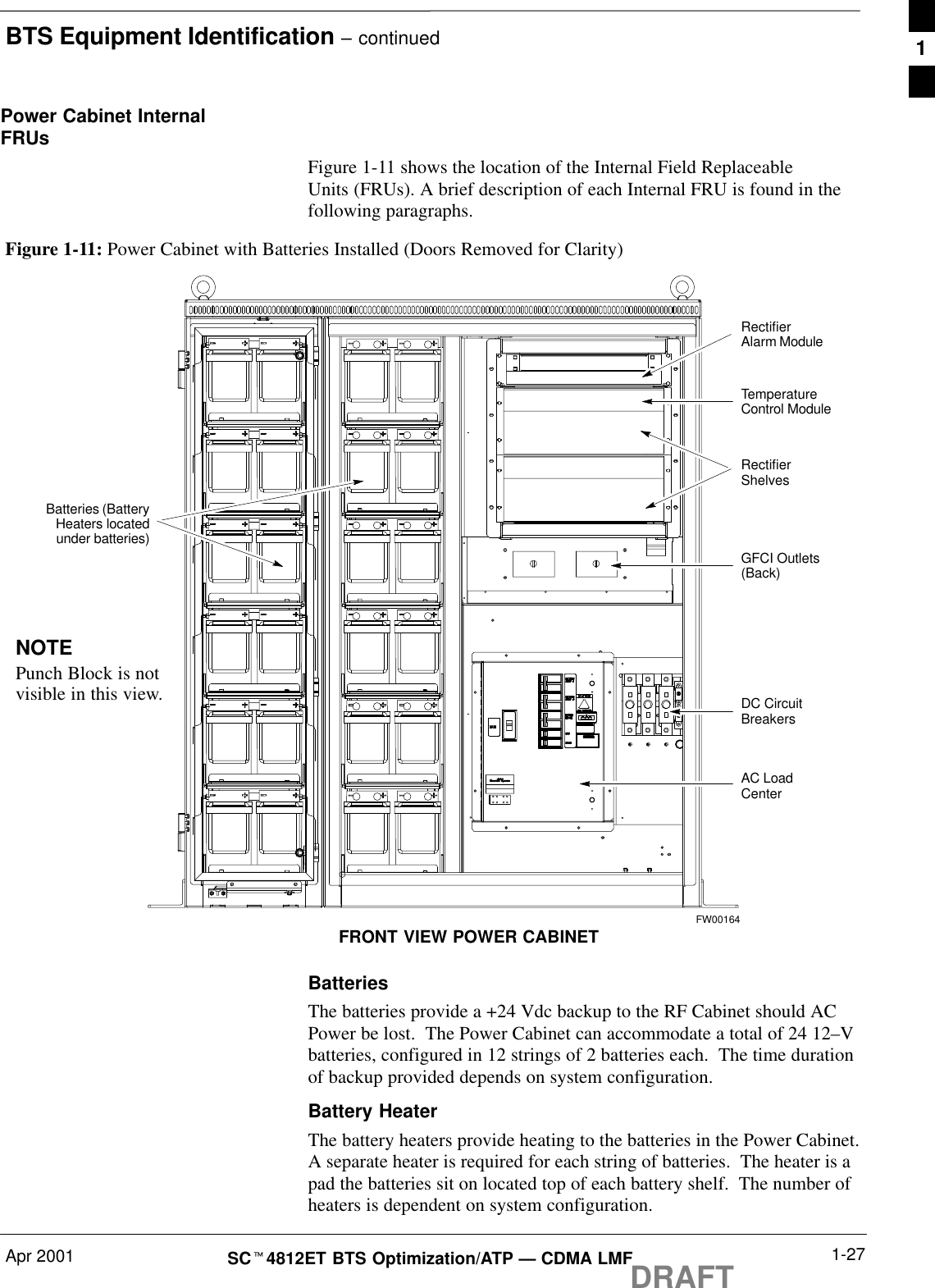
Nokia Solutions and Networks T5BQ1 Part 22 Cellular CDMA base station User Manual IHET5BQ1 Part 1 of 3

Nokia Solutions and Networks Part 22 Cellular CDMA base station IHET5BQ1 Part 1 of 3

IHET5BQ1 User Manual Part 1 of 3

BTS Optimization/ATPCDMA LMFSoftware Release 2.16.XSCt4812ET1.9 GHz and 800 MHz CDMAEnglishApr 200168P09253A74–O
DRAFTNoticeWhile reasonable efforts have been made to assure the accuracy of this document, Motorola, Inc. assumes no liability resulting fromany  inaccuracies or omissions in this document, or from use of the information obtained herein. The information in this document hasbeen carefully checked and is believed to be entirely reliable. However, no responsibility is assumed for inaccuracies or omissions.Motorola, Inc. reserves the right to make changes to any products described herein and reserves the right to revise this document andto make changes from time to time in content hereof with no obligation to notify any person of revisions or changes. Motorola, Inc.does not assume any liability arising out of the application or use of any product, software, or circuit described herein; neither does itconvey license under its patent rights or the rights of others.It is possible that this publication may contain references to, or information about Motorola products (machines and programs),programming, or services that are not announced in your country. Such references or information must not be construed to meanthat Motorola intends to announce such Motorola products, programming, or services in your country.CopyrightsThis instruction manual, and the Motorola products described in this instruction manual may be, include or describe copyrightedMotorola material, such as computer programs stored in semiconductor memories or other media. Laws in the United States andother countries preserve for Motorola certain exclusive rights for copyrighted material, including the exclusive right to copy,reproduce in any form, distribute and make derivative works of the copyrighted material. Accordingly, any copyrightedMotorola material contained herein or in the Motorola products described in this instruction manual may not be copied,reproduced, distributed, merged or modified in any manner without the express written permission of Motorola. Furthermore, thepurchase of Motorola products shall not be deemed to grant either directly or by implication, estoppel, or otherwise, any licenseunder the copyrights, patents or patent applications of Motorola, as arises by operation of law in the sale of a product.Usage and Disclosure RestrictionsLicense AgreementThe software described in this document is the property of Motorola, Inc. It is furnished by express license agreement only andmay be used only in accordance with the terms of such an agreement.Copyrighted MaterialsSoftware and documentation are copyrighted materials. Making unauthorized copies is prohibited by law. No part of thesoftware or documentation may be reproduced, transmitted, transcribed, stored in a retrieval system, or translated into anylanguage or computer language, in any form or by any means, without prior written permission of Motorola, Inc.High Risk ActivitiesComponents, units, or third–party products used in the product described herein are NOT fault–tolerant and are NOT designed,manufactured, or intended for use as on–line control equipment in the following hazardous environments requiring fail–safecontrols: the operation of Nuclear Facilities, Aircraft Navigation or Aircraft Communication Systems, Air Traffic Control, LifeSupport, or Weapons Systems (“High Risk Activities”). Motorola and its supplier(s) specifically disclaim any expressed orimplied warranty of fitness for such High Risk Activities.Trademarks and Motorola are registered trademarks of Motorola, Inc.Product and service names profiled herein are trademarks of Motorola, Inc. Other manufacturers’ products or services profiledherein may be referred to by trademarks of their respective companies.Copyright Copyright 2001 Motorola, Inc.  All Rights ReservedPrinted on    Recyclable PaperREV010598SPECIFICATIONS SUBJECT TO CHANGE WITHOUT NOTICE
Apr 2001 iSCt4812ET BTS Optimization/ATP — CDMA LMFDRAFTTable of ContentsSCt4812ET BTS Optimization/ATP — CDMA LMFCDMA 1.9 GHz and 800 MHzList of Figures iv. . . . . . . . . . . . . . . . . . . . . . . . . . . . . . . . . . . . . . . . . . . . . . . . . . . List of Tables vi. . . . . . . . . . . . . . . . . . . . . . . . . . . . . . . . . . . . . . . . . . . . . . . . . . . Product Information xi. . . . . . . . . . . . . . . . . . . . . . . . . . . . . . . . . . . . . . . . . . . . . . FCC Part 15 xii. . . . . . . . . . . . . . . . . . . . . . . . . . . . . . . . . . . . . . . . . . . . . . . . . . . . FCC Part 68 xiv. . . . . . . . . . . . . . . . . . . . . . . . . . . . . . . . . . . . . . . . . . . . . . . . . . . . Foreword xv. . . . . . . . . . . . . . . . . . . . . . . . . . . . . . . . . . . . . . . . . . . . . . . . . . . . . . . General Safety xviii. . . . . . . . . . . . . . . . . . . . . . . . . . . . . . . . . . . . . . . . . . . . . . . . . . . Revision History xx. . . . . . . . . . . . . . . . . . . . . . . . . . . . . . . . . . . . . . . . . . . . . . . . . Patent Notification xxi. . . . . . . . . . . . . . . . . . . . . . . . . . . . . . . . . . . . . . . . . . . . . . . Chapter 1: IntroductionOptimization Overview 1-1. . . . . . . . . . . . . . . . . . . . . . . . . . . . . . . . . . . . . . . . . . . . BTS Equipment Identification 1-13. . . . . . . . . . . . . . . . . . . . . . . . . . . . . . . . . . . . . . Chapter 2: Preliminary OperationsPreliminary Operations: Overview 2-1. . . . . . . . . . . . . . . . . . . . . . . . . . . . . . . . . . . Initial Power Up 2-3. . . . . . . . . . . . . . . . . . . . . . . . . . . . . . . . . . . . . . . . . . . . . . . . . Chapter 3: Optimization/CalibrationOptimization/Calibration – Introduction 3-1. . . . . . . . . . . . . . . . . . . . . . . . . . . . . . Isolate Span Lines/Connect LMF 3-4. . . . . . . . . . . . . . . . . . . . . . . . . . . . . . . . . . . . Preparing the LMF 3-10. . . . . . . . . . . . . . . . . . . . . . . . . . . . . . . . . . . . . . . . . . . . . . . Using CDMA LMF 3-21. . . . . . . . . . . . . . . . . . . . . . . . . . . . . . . . . . . . . . . . . . . . . . Download the BTS 3-27. . . . . . . . . . . . . . . . . . . . . . . . . . . . . . . . . . . . . . . . . . . . . . . CSM System Time – GPS & LFR/HSO Verification 3-32. . . . . . . . . . . . . . . . . . . . . Test Equipment Set–up 3-42. . . . . . . . . . . . . . . . . . . . . . . . . . . . . . . . . . . . . . . . . . . . Test Set Calibration 3-50. . . . . . . . . . . . . . . . . . . . . . . . . . . . . . . . . . . . . . . . . . . . . . . Bay Level Offset Calibration 3-59. . . . . . . . . . . . . . . . . . . . . . . . . . . . . . . . . . . . . . . RFDS Setup and Calibration 3-71. . . . . . . . . . . . . . . . . . . . . . . . . . . . . . . . . . . . . . . Alarms Testing 3-82. . . . . . . . . . . . . . . . . . . . . . . . . . . . . . . . . . . . . . . . . . . . . . . . . .  . . . continued on next page
Table of Contents – continuedDRAFTSCt4812ET BTS Optimization/ATP — CDMA LMF Apr 2001iiChapter 4: Automated Acceptance Test Procedure (ATP)Automated Acceptance Test Procedures – Overview 4-1. . . . . . . . . . . . . . . . . . . . . TX Spectral Purity Transmit Mask Acceptance Test 4-5. . . . . . . . . . . . . . . . . . . . . TX Waveform Quality (rho) Acceptance Test 4-7. . . . . . . . . . . . . . . . . . . . . . . . . . TX Pilot Time Offset Acceptance Test 4-8. . . . . . . . . . . . . . . . . . . . . . . . . . . . . . . . TX Code Domain Power Acceptance Test 4-9. . . . . . . . . . . . . . . . . . . . . . . . . . . . . RX Frame Error Rate (FER) Acceptance Test 4-11. . . . . . . . . . . . . . . . . . . . . . . . . . Generate an ATP Report 4-12. . . . . . . . . . . . . . . . . . . . . . . . . . . . . . . . . . . . . . . . . . . Chapter 5: Leaving the SiteExternal Test Equipment Removal 5-1. . . . . . . . . . . . . . . . . . . . . . . . . . . . . . . . . . . Reset All Devices 5-1. . . . . . . . . . . . . . . . . . . . . . . . . . . . . . . . . . . . . . . . . . . . . . . . Updating BTS CAL LMF Files in the CBSC 5-1. . . . . . . . . . . . . . . . . . . . . . . . . . BTS Site Span Configuration Verification 5-3. . . . . . . . . . . . . . . . . . . . . . . . . . . . . Set BTS Site Span Configuration 5-4. . . . . . . . . . . . . . . . . . . . . . . . . . . . . . . . . . . . Re–connect BTS T1 Spans and Integrated Frame Modem 5-6. . . . . . . . . . . . . . . . LMF Removal 5-6. . . . . . . . . . . . . . . . . . . . . . . . . . . . . . . . . . . . . . . . . . . . . . . . . . . Reestablish OMC-R Control/ Verifying T1/E1 5-7. . . . . . . . . . . . . . . . . . . . . . . . . Chapter 6: Basic TroubleshootingBasic Troubleshooting Overview 6-1. . . . . . . . . . . . . . . . . . . . . . . . . . . . . . . . . . . . Troubleshooting: Installation 6-2. . . . . . . . . . . . . . . . . . . . . . . . . . . . . . . . . . . . . . . Troubleshooting: Download 6-4. . . . . . . . . . . . . . . . . . . . . . . . . . . . . . . . . . . . . . . . Troubleshooting: Calibration 6-7. . . . . . . . . . . . . . . . . . . . . . . . . . . . . . . . . . . . . . . Troubleshooting: Transmit ATP 6-9. . . . . . . . . . . . . . . . . . . . . . . . . . . . . . . . . . . . . Troubleshooting: Receive ATP 6-11. . . . . . . . . . . . . . . . . . . . . . . . . . . . . . . . . . . . . . Troubleshooting: CSM Checklist 6-12. . . . . . . . . . . . . . . . . . . . . . . . . . . . . . . . . . . . C–CCP Backplane Troubleshooting 6-14. . . . . . . . . . . . . . . . . . . . . . . . . . . . . . . . . . RFDS – Fault Isolation 6-20. . . . . . . . . . . . . . . . . . . . . . . . . . . . . . . . . . . . . . . . . . . . Module Front Panel LED Indicators and Connectors 6-22. . . . . . . . . . . . . . . . . . . . . Basic Troubleshooting – Span Control Link 6-29. . . . . . . . . . . . . . . . . . . . . . . . . . . Appendix A: Data SheetsAppendix A: Optimization (Pre–ATP) Data Sheets A-1. . . . . . . . . . . . . . . . . . . . . . Appendix A: Site Serial Number Check List A-17. . . . . . . . . . . . . . . . . . . . . . . . . . . Appendix B: FRU Optimization/ATP Test MatrixAppendix B: FRU Optimization/ATP Test Matrix B-1. . . . . . . . . . . . . . . . . . . . . . .  . . . continued on next page
Table of Contents – continuedApr 2001 iiiSCt4812ET BTS Optimization/ATP — CDMA LMFDRAFTAppendix C: BBX Gain Set Point vs. BTS Output ConsiderationsAppendix C: BBX2 Gain Set Point vs. BTS Output Considerations C-1. . . . . . . . . Appendix D: CDMA Operating Frequency InformationCDMA Operating Frequency Programming Information – NorthAmerican PCS Bands D-1. . . . . . . . . . . . . . . . . . . . . . . . . . . . . . . . . . . . . . . . . . . . . Appendix E: PN Offset/I & Q Offset Register Programming InformationAppendix E: PN Offset Programming Information E-1. . . . . . . . . . . . . . . . . . . . . . Appendix F: Test Equipment PreparationTest Equipment Preparation F-1. . . . . . . . . . . . . . . . . . . . . . . . . . . . . . . . . . . . . . . . Manual Cable Calibration F-10. . . . . . . . . . . . . . . . . . . . . . . . . . . . . . . . . . . . . . . . . . Appendix G: In–Service CalibrationIntroduction G-1. . . . . . . . . . . . . . . . . . . . . . . . . . . . . . . . . . . . . . . . . . . . . . . . . . . . . Power Delta Calibration G-2. . . . . . . . . . . . . . . . . . . . . . . . . . . . . . . . . . . . . . . . . . . In–Service Calibration G-10. . . . . . . . . . . . . . . . . . . . . . . . . . . . . . . . . . . . . . . . . . . . Index Index-1. . . . . . . . . . . . . . . . . . . . . . . . . . . . . . . . . . . . . . . . . . . . . . . . . . . . . . . . . . . . . . . . . . . . . . . . . . . . . .
DRAFTSCt4812ET BTS Optimization/ATP — CDMA LMF Apr 2001ivList of FiguresSCt4812ET BTS Optimization/ATP — CDMA LMFCDMA 1.9 GHz and 800 MHzFigure 1-1: Null Modem Cable Detail 1-7. . . . . . . . . . . . . . . . . . . . . . . . . . . . . . . . Figure 1-2: Typical Logical BTS Configurations 1-15. . . . . . . . . . . . . . . . . . . . . . . . Figure 1-3: SC 4812ET RF Cabinet 1-16. . . . . . . . . . . . . . . . . . . . . . . . . . . . . . . . . . Figure 1-4: RF Cabinet Internal FRUs 1-17. . . . . . . . . . . . . . . . . . . . . . . . . . . . . . . . Figure 1-5: SC 4812ET C–CCP Shelf 1-19. . . . . . . . . . . . . . . . . . . . . . . . . . . . . . . . Figure 1-6:  SC 4812ET Intercabinet I/O Detail (Rear View) 1-20. . . . . . . . . . . . . . Figure 1-7: SC 4812ET  I/O Plate Diagram 1-21. . . . . . . . . . . . . . . . . . . . . . . . . . . . Figure 1-8: RFDS Location in an SC 4812ET RF Cabinet 1-22. . . . . . . . . . . . . . . . Figure 1-9: SC4812ET LPA Configuration with Combiners/Filters 1-25. . . . . . . . . Figure 1-10: Power Cabinet 1-26. . . . . . . . . . . . . . . . . . . . . . . . . . . . . . . . . . . . . . . . Figure 1-11: Power Cabinet with Batteries Installed (Doors Removedfor Clarity) 1-27. . . . . . . . . . . . . . . . . . . . . . . . . . . . . . . . . . . . . . . . . . . . . . . . . . . . . Figure 2-1: Backplane DIP Switch Settings 2-2. . . . . . . . . . . . . . . . . . . . . . . . . . . . Figure 2-2: AC Load Center Wiring 2-5. . . . . . . . . . . . . . . . . . . . . . . . . . . . . . . . . . Figure 2-3: Meter Alarm Panel 2-6. . . . . . . . . . . . . . . . . . . . . . . . . . . . . . . . . . . . . . Figure 2-4: Temperature Compensation Panel 2-6. . . . . . . . . . . . . . . . . . . . . . . . . . Figure 2-5: RF Cabinet Circuit Breaker Panel and 27V DC Terminal Locations 2-9Figure 2-6: Heat Exchanger Blower Assembly 2-12. . . . . . . . . . . . . . . . . . . . . . . . . Figure 2-7: Power Cabinet Circuit Breaker Assemblies 2-13. . . . . . . . . . . . . . . . . . . Figure 2-8: Power Cabinet AC Circuit Breakers 2-14. . . . . . . . . . . . . . . . . . . . . . . . Figure 2-9: Power Cabinet DC Circuit Breakers 2-15. . . . . . . . . . . . . . . . . . . . . . . . Figure 3-1: Back and Front View of the CSU 3-5. . . . . . . . . . . . . . . . . . . . . . . . . . Figure 3-2: 50 Pair Punch Block 3-6. . . . . . . . . . . . . . . . . . . . . . . . . . . . . . . . . . . . Figure 3-3: LMF Folder Structure 3-16. . . . . . . . . . . . . . . . . . . . . . . . . . . . . . . . . . . Figure 3-4: LMF Connection Detail 3-18. . . . . . . . . . . . . . . . . . . . . . . . . . . . . . . . . . Figure 3-5: BTS Ethernet LAN Interconnect Diagram 3-19. . . . . . . . . . . . . . . . . . . Figure 3-6: CDMA LMF Computer Common MMI Connections 3-26. . . . . . . . . . . Figure 3-7: CSM MMI Terminal Connection 3-35. . . . . . . . . . . . . . . . . . . . . . . . . . . Figure 3-8: Cable Calibration Test Setup 3-45. . . . . . . . . . . . . . . . . . . . . . . . . . . . . .  . . . continued on next page
List of Figures – continuedApr 2001 vSCt4812ET BTS Optimization/ATP — CDMA LMFDRAFTFigure 3-9: TX Calibration Test Setup (CyberTest and HP 8935) 3-46. . . . . . . . . . . Figure 3-10: TX Calibration Test Setup HP 8921A and Advantest 3-47. . . . . . . . . . Figure 3-11: Optimization/ATP Test Setup Calibration (CyberTest,HP 8935 and Advantest) 3-48. . . . . . . . . . . . . . . . . . . . . . . . . . . . . . . . . . . . . . . . . . . Figure 3-12: Optimization/ATP Test Setup HP 8921A 3-49. . . . . . . . . . . . . . . . . . . Figure 3-13:  Calibrating Test Equipment Setup for TX Cable Calibration(Using Signal Generator and Spectrum Analyzer) 3-55. . . . . . . . . . . . . . . . . . . . . . . Figure 3-14:  Calibrating Test Equipment Setup for RX ATP Test(Using Signal Generator and Spectrum Analyzer) 3-56. . . . . . . . . . . . . . . . . . . . . . . Figure 3-15: Battery Overtemperature Sensor 3-87. . . . . . . . . . . . . . . . . . . . . . . . . . Figure 3-16: Location of Connector J8 on the Meter Alarm Panel 3-89. . . . . . . . . . Figure 4-1: TX Mask Verification Spectrum Analyzer Display 4-6. . . . . . . . . . . . . Figure 4-2: Code Domain Power and Noise Floor Levels 4-10. . . . . . . . . . . . . . . . . Figure 6-1: CSM Front Panel Indicators & Monitor Ports 6-22. . . . . . . . . . . . . . . . . Figure 6-2: GLI2 Front Panel Operating Indicators 6-25. . . . . . . . . . . . . . . . . . . . . . Figure 6-3: MCC24/8E Front Panel LEDs and LED Indicators 6-27. . . . . . . . . . . . Figure D-1: North America PCS Frequency Spectrum (CDMA Allocation) D-1. . . Figure D-2: North American Cellular Telephone System FrequencySpectrum (CDMA Allocation). D-4. . . . . . . . . . . . . . . . . . . . . . . . . . . . . . . . . . . . . Figure F-1: HP8921A/600 Cables Connection for 10 MHz Signal andGPIB without Rubidium F-2. . . . . . . . . . . . . . . . . . . . . . . . . . . . . . . . . . . . . . . . . . . Figure F-2: HP8921A Cables Connection for 10 MHz Signal and GPIBwith Rubidium F-4. . . . . . . . . . . . . . . . . . . . . . . . . . . . . . . . . . . . . . . . . . . . . . . . . . Figure F-3: Cable Connections for Test Set without 10 MHzRubidium Standard F-7. . . . . . . . . . . . . . . . . . . . . . . . . . . . . . . . . . . . . . . . . . . . . . . Figure F-4: Cable Connections for Test Set with 10 MHzRubidium Standard F-8. . . . . . . . . . . . . . . . . . . . . . . . . . . . . . . . . . . . . . . . . . . . . . . Figure F-5: Cable CalibrationUsing HP8921 with PCS Interface F-13. . . . . . . . . . . Figure F-6: Cable Calibration using Advantest R3465 F-16. . . . . . . . . . . . . . . . . . . Figure F-7: Power Meter Detail F-17. . . . . . . . . . . . . . . . . . . . . . . . . . . . . . . . . . . . . Figure F-8: Gigatronics 8542C Power Meter Detail F-20. . . . . . . . . . . . . . . . . . . . . Figure G-1: Delta Calibration Setup – HP8921A to HP437B G-4. . . . . . . . . . . . . . Figure G-2: Delta Calibration Setup – HP8921A to HP8921A G-4. . . . . . . . . . . . . Figure G-3: Delta Calibration Setup – R3561L to HP437B G-6. . . . . . . . . . . . . . . Figure G-4: Delta Calibration Setup – R3561L to R3465 G-7. . . . . . . . . . . . . . . . . Figure G-5: Delta Calibration Setup – HP8935 to HP437B G-8. . . . . . . . . . . . . . . Figure G-6: Delta Calibration Setup – HP8935 to HP8935 G-9. . . . . . . . . . . . . . . . Figure G-7: Optimization/ATP Test Setup Using Directional Coupler G-11. . . . . . . Figure G-8: Optimization/ATP Test Setup Using RFDS G-12. . . . . . . . . . . . . . . . . .  . . . continued on next page
DRAFTSCt4812ET BTS Optimization/ATP — CDMA LMF Apr 2001viList of TablesSCt4812ET BTS Optimization/ATP — CDMA LMFCDMA 1.9 GHz and 800 MHzTable 1-1: CDMA LMF Test Equipment Support Table 1-4. . . . . . . . . . . . . . . . . . Table 1-2: Abbreviations and Acronyms 1-11. . . . . . . . . . . . . . . . . . . . . . . . . . . . . . Table 1-3: C–CCP Shelf/Cage Card/Module Device IDNumbers (Top Shelf) 1-14. . . . . . . . . . . . . . . . . . . . . . . . . . . . . . . . . . . . . . . . . . . . . Table 1-4: C–CCP Shelf/Cage Card/Module Device IDNumbers (Bottom Shelf) 1-14. . . . . . . . . . . . . . . . . . . . . . . . . . . . . . . . . . . . . . . . . . . Table 1-5: BTS Sector Configuration 1-23. . . . . . . . . . . . . . . . . . . . . . . . . . . . . . . . . Table 1-6: Sector Configurations 1-24. . . . . . . . . . . . . . . . . . . . . . . . . . . . . . . . . . . . Table 2-1: Initial Installation of Boards/Modules 2-1. . . . . . . . . . . . . . . . . . . . . . . . Table 2-2: Initial Inspection and Setup 2-3. . . . . . . . . . . . . . . . . . . . . . . . . . . . . . . . Table 2-3: AC Voltage Measurements 2-4. . . . . . . . . . . . . . . . . . . . . . . . . . . . . . . . Table 2-4: Applying AC Power 2-5. . . . . . . . . . . . . . . . . . . . . . . . . . . . . . . . . . . . . Table 2-5: Power Cabinet Power Up Tests 2-6. . . . . . . . . . . . . . . . . . . . . . . . . . . . . Table 2-6: DC Power Pre–test (BTS Frame) 2-7. . . . . . . . . . . . . . . . . . . . . . . . . . . Table 2-7: RF Cabinet Power Up 2-8. . . . . . . . . . . . . . . . . . . . . . . . . . . . . . . . . . . . Table 2-8: Battery Charge Test (Connected Batteries) 2-10. . . . . . . . . . . . . . . . . . . . Table 2-9: Battery Discharge Test 2-11. . . . . . . . . . . . . . . . . . . . . . . . . . . . . . . . . . . . Table 2-10: Heat Exchanger Power Up 2-11. . . . . . . . . . . . . . . . . . . . . . . . . . . . . . . Table 3-2: T1/E1 Span Isolation 3-9. . . . . . . . . . . . . . . . . . . . . . . . . . . . . . . . . . . . . Table 3-3: LMF Operating System Installation 3-10. . . . . . . . . . . . . . . . . . . . . . . . . Table 3-4: Copying CBSC CDF Files to the LMF 3-12. . . . . . . . . . . . . . . . . . . . . . . Table 3-5: Creating a Named Hyperlink Connection for MMI Connection 3-14. . . . Table 3-6: LMF   to BTS Connection 3-17. . . . . . . . . . . . . . . . . . . . . . . . . . . . . . . . . Table 3-7: Pinging the Processors 3-20. . . . . . . . . . . . . . . . . . . . . . . . . . . . . . . . . . . . Table 3-8: BTS GUI Login Procedure 3-23. . . . . . . . . . . . . . . . . . . . . . . . . . . . . . . . Table 3-9: BTS CLI Login Procedure 3-24. . . . . . . . . . . . . . . . . . . . . . . . . . . . . . . . Table 3-10: BTS GUI Logout Procedure 3-24. . . . . . . . . . . . . . . . . . . . . . . . . . . . . . Table 3-11: BTS CLI Logout Procedure 3-25. . . . . . . . . . . . . . . . . . . . . . . . . . . . . . . Table 3-12: Establishing MMI Communications 3-26. . . . . . . . . . . . . . . . . . . . . . . . Table 3-13: Download and Enable MGLI2 3-28. . . . . . . . . . . . . . . . . . . . . . . . . . . .  . . . continued on next page
List of Tables – continuedApr 2001 viiSCt4812ET BTS Optimization/ATP — CDMA LMFDRAFTTable 3-14: Download Code and Data to Non–MGLI Devices 3-29. . . . . . . . . . . . . Table 3-15: Select CSM Clock Source 3-29. . . . . . . . . . . . . . . . . . . . . . . . . . . . . . . . Table 3-16: Enable CSMs 3-30. . . . . . . . . . . . . . . . . . . . . . . . . . . . . . . . . . . . . . . . . . Table 3-17: Enable MCCs 3-31. . . . . . . . . . . . . . . . . . . . . . . . . . . . . . . . . . . . . . . . . Table 3-18: Test Equipment Setup (GPS & LFR/HSO Verification) 3-34. . . . . . . . . Table 3-19: GPS Initialization/Verification 3-36. . . . . . . . . . . . . . . . . . . . . . . . . . . . Table 3-20: LORAN–C Initialization/Verification 3-40. . . . . . . . . . . . . . . . . . . . . . . Table 3-21: Test Equipment Setup 3-43. . . . . . . . . . . . . . . . . . . . . . . . . . . . . . . . . . . Table 3-22: Selecting Test Equipment Manually in a Serial Connection Tab 3-51. . Table 3-23: Selecting Test Equipment Using Auto-Detect 3-52. . . . . . . . . . . . . . . . . Table 3-24: Test Equipment Calibration 3-53. . . . . . . . . . . . . . . . . . . . . . . . . . . . . . . Table 3-25: Cable Calibration 3-54. . . . . . . . . . . . . . . . . . . . . . . . . . . . . . . . . . . . . . . Table 3-26: Calibrating TX Cables Using Signal Generator andSpectrum Analyzer 3-55. . . . . . . . . . . . . . . . . . . . . . . . . . . . . . . . . . . . . . . . . . . . . . . Table 3-27: Calibrating RX Cables Using a Signal Generator andSpectrum Analyzer 3-56. . . . . . . . . . . . . . . . . . . . . . . . . . . . . . . . . . . . . . . . . . . . . . . Table 3-28: Setting Cable Loss Values 3-57. . . . . . . . . . . . . . . . . . . . . . . . . . . . . . . . Table 3-29: Setting TX Coupler Loss Values 3-58. . . . . . . . . . . . . . . . . . . . . . . . . . . Table 3-30: BLO BTS.cal file Array Branch Assignments 3-61. . . . . . . . . . . . . . . . Table 3-31: BTS.cal File Array (Per Sector) 3-62. . . . . . . . . . . . . . . . . . . . . . . . . . . Table 3-32: Test Equipment Setup (RF Path Calibration) 3-63. . . . . . . . . . . . . . . . . Table 3-33: BTS TX Path Calibration 3-65. . . . . . . . . . . . . . . . . . . . . . . . . . . . . . . . Table 3-34: Download BLO 3-66. . . . . . . . . . . . . . . . . . . . . . . . . . . . . . . . . . . . . . . . Table 3-35: TX Path Audit 3-68. . . . . . . . . . . . . . . . . . . . . . . . . . . . . . . . . . . . . . . . . Table 3-36: All Cal/Audit Test 3-69. . . . . . . . . . . . . . . . . . . . . . . . . . . . . . . . . . . . . . Table 3-37: Create CAL File 3-70. . . . . . . . . . . . . . . . . . . . . . . . . . . . . . . . . . . . . . . Table 3-38: RFDS Parameter Settings 3-72. . . . . . . . . . . . . . . . . . . . . . . . . . . . . . . . Table 3-39: Definition of Parameters 3-73. . . . . . . . . . . . . . . . . . . . . . . . . . . . . . . . . Table 3-40: Valid NAM Field Ranges 3-74. . . . . . . . . . . . . . . . . . . . . . . . . . . . . . . . Table 3-41: Measuring Directional Coupler Loss 3-75. . . . . . . . . . . . . . . . . . . . . . . . Table 3-42: Set Antenna Map Data 3-77. . . . . . . . . . . . . . . . . . . . . . . . . . . . . . . . . . . Table 3-43: Set RFDS Configuration Data 3-78. . . . . . . . . . . . . . . . . . . . . . . . . . . . . Table 3-44: RFDS Calibration 3-80. . . . . . . . . . . . . . . . . . . . . . . . . . . . . . . . . . . . . . Table 3-45: Program NAM Procedure 3-81. . . . . . . . . . . . . . . . . . . . . . . . . . . . . . . . Table 3-46: Heat Exchanger Alarm 3-83. . . . . . . . . . . . . . . . . . . . . . . . . . . . . . . . . . Table 3-47: Door Alarm 3-83. . . . . . . . . . . . . . . . . . . . . . . . . . . . . . . . . . . . . . . . . . . Table 3-48: AC Fail Alarm 3-83. . . . . . . . . . . . . . . . . . . . . . . . . . . . . . . . . . . . . . . . .  . . . continued on next page
List of Tables  – continuedDRAFTSCt4812ET BTS Optimization/ATP — CDMA LMF Apr 2001viiiTable 3-49: Minor Alarm 3-84. . . . . . . . . . . . . . . . . . . . . . . . . . . . . . . . . . . . . . . . . . Table 3-50: Single Rectifier Fail or Minor Alarm 3-84. . . . . . . . . . . . . . . . . . . . . . . Table 3-51: Multiple Rectifier Failure or Major Alarm 3-85. . . . . . . . . . . . . . . . . . . Table 3-52: Single Rectifier Fail or Minor Alarm 3-85. . . . . . . . . . . . . . . . . . . . . . . Table 3-53: Multiple Rectifier Failure or Major Alarm 3-85. . . . . . . . . . . . . . . . . . . Table 3-54: Battery Over Temperature Alarm 3-86. . . . . . . . . . . . . . . . . . . . . . . . . . Table 3-55: Rectifier Over Temperature Alarm 3-88. . . . . . . . . . . . . . . . . . . . . . . . . Table 3-56: Check Before Leaving the Site 3-89. . . . . . . . . . . . . . . . . . . . . . . . . . . . Table 4-1:  ATP Test Procedure 4-4. . . . . . . . . . . . . . . . . . . . . . . . . . . . . . . . . . . . . Table 4-2:  Generate an ATP  Report  4-12. . . . . . . . . . . . . . . . . . . . . . . . . . . . . . . . . Table 5-1: External Test Equipment Removal 5-1. . . . . . . . . . . . . . . . . . . . . . . . . . Table 5-2: Copy Files from LMF to a Diskette 5-1. . . . . . . . . . . . . . . . . . . . . . . . . Table 5-3: Copy CAL Files From Diskette to the CBSC 5-2. . . . . . . . . . . . . . . . . . Table 5-4: T1/E1 Span/IFM Connections 5-3. . . . . . . . . . . . . . . . . . . . . . . . . . . . . . Table 5-5: Terminate the LMF Session and Remove the LMF 5-3. . . . . . . . . . . . . Table 6-1:  Login Failure Troubleshooting Procedure 6-2. . . . . . . . . . . . . . . . . . . . Table 6-2:  Troubleshooting a Power Meter Communication Failure 6-2. . . . . . . . Table 6-3:  Troubleshooting a Communications AnalyzerCommunication Failure 6-3. . . . . . . . . . . . . . . . . . . . . . . . . . . . . . . . . . . . . . . . . . . Table 6-4: Troubleshooting Code Download Failure 6-4. . . . . . . . . . . . . . . . . . . . . Table 6-5: Troubleshooting Data Download Failure 6-4. . . . . . . . . . . . . . . . . . . . . Table 6-6: Troubleshooting Device Enable (INS) Failure 6-5. . . . . . . . . . . . . . . . . Table 6-7: LPA Errors 6-5. . . . . . . . . . . . . . . . . . . . . . . . . . . . . . . . . . . . . . . . . . . . . Table 6-8: Troubleshooting BLO Calibration Failure 6-6. . . . . . . . . . . . . . . . . . . . Table 6-9: Troubleshooting Calibration Audit Failure 6-7. . . . . . . . . . . . . . . . . . . . Table 6-10: Troubleshooting TX Mask Measurement Failure 6-8. . . . . . . . . . . . . . Table 6-11: Troubleshooting Rho and Pilot Time Offset Measurement Failure 6-8. Table 6-12: Troubleshooting Code Domain Power and Noise FloorMeasurement Failure 6-9. . . . . . . . . . . . . . . . . . . . . . . . . . . . . . . . . . . . . . . . . . . . . Table 6-13: Troubleshooting Carrier Measurement Failure 6-9. . . . . . . . . . . . . . . . Table 6-14: Troubleshooting Multi-FER Failure 6-10. . . . . . . . . . . . . . . . . . . . . . . . Table 6-15: No GLI2 Control via LMF (all GLI2s) 6-15. . . . . . . . . . . . . . . . . . . . . . Table 6-16: No GLI2 Control through Span Line Connection (Both GLI2s) 6-15. . Table 6-17: MGLI2 Control Good – No Control over Co–located GLI2 6-15. . . . . Table 6-18: MGLI2 Control Good – No Control over AMR 6-16. . . . . . . . . . . . . . . Table 6-19: MGLI2 Control Good – No Control over Co–located GLI2s 6-16. . . . . Table 6-20: BBX2 Control Good – No (or Missing) Span Line Traffic 6-16. . . . . . .  . . . continued on next page
List of Tables – continuedApr 2001 ixSCt4812ET BTS Optimization/ATP — CDMA LMFDRAFTTable 6-21: No MCC24 Channel Elements 6-16. . . . . . . . . . . . . . . . . . . . . . . . . . . . Table 6-22: No DC Input Voltage to Power Supply Module 6-17. . . . . . . . . . . . . . . Table 6-23: No DC Input Voltage to any C–CCP Shelf Module 6-18. . . . . . . . . . . . Table 6-24: No DC Input Voltage to any C–CCP Shelf Module 6-18. . . . . . . . . . . . Table 6-25: RFDS Fault Isolation – All tests fail 6-19. . . . . . . . . . . . . . . . . . . . . . . . Table 6-26: RFDS Fault Isolation – All RX and TX paths fail 6-19. . . . . . . . . . . . . Table 6-27: RFDS Fault Isolation – All tests fail on single antenna path 6-20. . . . . Table 6-28: Troubleshooting Control Link Failure 6-28. . . . . . . . . . . . . . . . . . . . . . . Table A-1: Verification of Test Equipment Used A-1. . . . . . . . . . . . . . . . . . . . . . . . Table A-2: Site Checklist A-2. . . . . . . . . . . . . . . . . . . . . . . . . . . . . . . . . . . . . . . . . . Table A-3: Preliminary Operations A-2. . . . . . . . . . . . . . . . . . . . . . . . . . . . . . . . . . . Table A-4: GPS Receiver Operation A-5. . . . . . . . . . . . . . . . . . . . . . . . . . . . . . . . . . Table A-5: LFR Receiver Operation A-6. . . . . . . . . . . . . . . . . . . . . . . . . . . . . . . . . . Table A-6: LPA IM Reduction A-7. . . . . . . . . . . . . . . . . . . . . . . . . . . . . . . . . . . . . . Table A-7: TX BLO Calibration (3–Sector: 1–Carrier,  2–Carrierand 4–Carrier Non–adjacent Channels) A-8. . . . . . . . . . . . . . . . . . . . . . . . . . . . . . . Table A-8: TX Bay Level Offset Calibration (3–Sector: 2–CarrierAdjacent Channels) A-10. . . . . . . . . . . . . . . . . . . . . . . . . . . . . . . . . . . . . . . . . . . . . . . Table A-9: TX Bay Level Offset Calibration (3–Sector: 3 or4–Carrier Adjacent Channels) A-11. . . . . . . . . . . . . . . . . . . . . . . . . . . . . . . . . . . . . . . Table A-10: TX BLO Calibration (6–Sector: 1–Carrier, 2–CarrierNon–adjacent Channels) A-13. . . . . . . . . . . . . . . . . . . . . . . . . . . . . . . . . . . . . . . . . . . Table A-11: TX Antenna VSWR A-15. . . . . . . . . . . . . . . . . . . . . . . . . . . . . . . . . . . . Table A-12: RX Antenna VSWR A-16. . . . . . . . . . . . . . . . . . . . . . . . . . . . . . . . . . . . Table A-13: CDI Alarm Input Verification A-16. . . . . . . . . . . . . . . . . . . . . . . . . . . . . Table B-1: When RF Optimization Is required on the BTS B-1. . . . . . . . . . . . . . . . Table B-2: When to Optimize Inter–frame Cabling B-2. . . . . . . . . . . . . . . . . . . . . . Table B-3: SC 4812ET BTS Optimization and ATP Test Matrix B-4. . . . . . . . . . . Table C-1: BBX2 Gain Set Point vs. Actual BTS Output (in dBm) C-1. . . . . . . . . Table D-1: 1900 MHz TX and RX Frequency vs. Channel D-2. . . . . . . . . . . . . . . . Table D-2: 800 MHz TX and RX Frequency vs. Channel D-4. . . . . . . . . . . . . . . . . Table E-1: PnMaskI and PnMaskQ Values for PilotPn E-3. . . . . . . . . . . . . . . . . . . Table F-1: HP8921A/600 Communications Test Set Rear PanelConnections Without Rubidium F-1. . . . . . . . . . . . . . . . . . . . . . . . . . . . . . . . . . . . . Table F-2: HP8921A/600 Communications Test Set Rear PanelConnections With Rubidium F-3. . . . . . . . . . . . . . . . . . . . . . . . . . . . . . . . . . . . . . . Table F-3: System Connectivity F-5. . . . . . . . . . . . . . . . . . . . . . . . . . . . . . . . . . . . . Table F-4: Setting HP8921A GPIB Address F-6. . . . . . . . . . . . . . . . . . . . . . . . . . . Table F-5: Pretest Setup for HP8921A F-6. . . . . . . . . . . . . . . . . . . . . . . . . . . . . . . .  . . . continued on next page
List of Tables  – continuedDRAFTSCt4812ET BTS Optimization/ATP — CDMA LMF Apr 2001xTable F-6: Pretest Setup for HP8935 F-6. . . . . . . . . . . . . . . . . . . . . . . . . . . . . . . . . Table F-7: Advantest R3465 GPIB Address and Clock Setup F-9. . . . . . . . . . . . . . Table F-8: Pretest Setup for Advantest R346 F-9. . . . . . . . . . . . . . . . . . . . . . . . . . . Table F-9: Calibrating Test Cable Setup (using the HP PCS Interface) F-10. . . . . . . Table F-10: Procedure for Calibrating Test Cable Setup UsingAdvantest R3465 F-14. . . . . . . . . . . . . . . . . . . . . . . . . . . . . . . . . . . . . . . . . . . . . . . . Table F-11: Power Meter Calibration Procedure F-17. . . . . . . . . . . . . . . . . . . . . . . . Table F-12: Calibrate Gigatronics 8542 Power Meter F-19. . . . . . . . . . . . . . . . . . . . Table G-1: HP8921A Power Delta Calibration Procedure G-2. . . . . . . . . . . . . . . . . Table G-2: Advantest Power Delta Calibration Procedure G-4. . . . . . . . . . . . . . . . . Table G-3: HP8935 Power Delta Calibration Procedure G-7. . . . . . . . . . . . . . . . . . Table G-4: In–Service Calibration G-13. . . . . . . . . . . . . . . . . . . . . . . . . . . . . . . . . . .
Product InformationApr 2001 xi68P09253A74SCt4812ET BTS Optimization/ATP — CDMA LMFDRAFTModel & Options ChartsRefer to the SC 4812ET Field Replaceable Units manual(68P64113A24) for detailed model structure and option informationThis document covers only the steps required to verify the functionalityof  the Base transceiver Subsystem (BTS) equipment prior to systemlevel testing, and is intended to supplement site specific applicationinstructions.  It also should be used in conjunction with existing  productmanuals.  Additional steps may be required.
FCC Part 15DRAFTSCt4812ET BTS Optimization/ATP — CDMA LMF Apr 2001xiiFCC Part 15 RequirementsThis section conveys FCC Part 15 requirements for the T/ET/ETL seriesBTS cabinets.Part 15.19a(3) – INFORMATION TO USERThis device complies with Part 15 of the FCC Rules.Operation is subject to the following two conditions:(1) this device may not cause harmful interference, and(2) this device must accept any interference received,including interference that may cause undesired operation.NOTEPart 15.21 – INFORMATION TO USERChanges or modifications not expressly approved byMotorola could void your authority to operate theequipment.CAUTION
FCC Part 15 – continuedApr 2001 xiiiSCt4812ET BTS Optimization/ATP — CDMA LMFDRAFT15.105(b) – INFORMATION TO USERThis equipment has been tested and found to comply withthe limits for a Class B digital device, pursuant to Part 15of the FCC Rules. These limits are designed to providereasonable protection against harmful interference in aresidential installation. This equipment generates, uses andcan radiate radio frequency energy and, if not installed andused in accordance with the instructions, may causeharmful interference to radio communications. However,there is no guarantee that interference will not occur in aparticular installation. If this equipment does cause harmfulinterference to radio or television reception, which can bedetermined by turning the equipment OFF and ON, theuser is encouraged to try to correct the interference by oneor more of the following measures:–Reorient or relocate the receiving antenna.–Increase the separation between the equipment and re-ceiver.–Connect the equipment into an outlet on a circuit differ-ent from that to which the receiver is connected.–Consult the dealer or an experienced radio/TV technicianfor help.NOTE
FCC Part 68DRAFTSCt4812ET BTS Optimization/ATP — CDMA LMF Apr 2001xivFCC Part 68 RequirementsThis equipment complies with Part 68 of the Federal CommunicationsCommission (FCC) Rules and regulations. A label inside the cabinetframe easily visible with the door open in the upper portion of thecabinet contains, among other information, the FCC RegistrationNumber and Ringer Equivalence Number (REN) for this equipment. Ifrequested, this information must be provided to the telephone company.The REN is useful to determine the quantity of the devices which mayconnect to the telephone line. Excessive RENs on the telephone line mayresult in the devices not ringing in response to incoming calls. In most,but not all areas, the sum of the RENs should not exceed five (5.0). Tobe certain of the number of devices that may be connected to the line asdetermined by the total RENs, contact the telephone company todetermine the maximum REN for the calling area.If the dial–in site access modem causes harm to the telephone network,the telephone company will notify you in advance that temporarydiscontinuance of service may be required. If advance notice is notpractical, the telephone company will notify you of the discontinuance assoon as possible. Also, you will be advised of your right to file acomplaint with the FCC if you believe it is necessary.The telephone company may make changes in its facilities, equipment,operations, or procedures that could affect the operation of your dial–insite access modem. If this happens, the telephone company will provideadvance notice so that you can modify your equipment as required tomaintain uninterrupted service.If you experience trouble with the dial–in site access modem, pleasecontact:Motorola Cellular Service Center (MCSC)1501 W. Shure DriveArlington Heights, Illinois 60004Phone Number: (847) 632–5390for repair and/or warranty information. If the trouble is causing harm tothe telephone network, the telephone company may request you todisconnect the equipment from the network until the problem is solved.You should not attempt to repair this equipment yourself. Thisequipment contains no customer or user–serviceable parts.Changes or modifications not expressly approved by Motorola couldvoid your authority to operate this equipment.
ForewordApr 2001 xvSCt4812ET BTS Optimization/ATP — CDMA LMFDRAFTScope of manualThis manual is intended for use by cellular telephone systemcraftspersons in the day-to-day operation of Motorola cellular systemequipment and ancillary devices. It is assumed that the user of thisinformation has a general understanding of telephony, as used in theoperation of the Public Switched Telephone Network (PSTN), and isfamiliar with these concepts as they are applied in the cellularmobile/portable radiotelephone environment. The user, however, is notexpected to have any detailed technical knowledge of the internaloperation of the equipment.This manual is not intended to replace the system and equipmenttraining offered by Motorola, although it can be used to supplement orenhance the knowledge gained through such training.Text conventionsThe following special paragraphs are used in this manual to point outinformation that must be read. This information may be set-off from thesurrounding text, but is always preceded by a bold title in capital letters.The four categories of these special paragraphs are:Presents additional, helpful, non-critical information thatyou can use.NOTEPresents information to help you avoid an undesirablesituation or provides additional information to help youunderstand a topic or concept.IMPORTANT*Presents information to identify a situation in whichequipment damage could occur, thus avoiding damage toequipment.CAUTIONPresents information to warn you of a potentiallyhazardous situation in which there is a possibility ofpersonal injury.WARNING . . . continued on next page
Foreword – continuedDRAFTSCt4812ET BTS Optimization/ATP — CDMA LMF Apr 2001xviThe following typographical conventions are used for the presentation ofsoftware information:In text, typewriter style characters representprompts and the system output as displayed on a Hyperterminal screen.Changes to manualChanges that occur after the printing date are incorporated into yourmanual by Cellular Manual Revisions (CMRs). The information in thismanual is updated, as required, by a CMR when new options andprocedures become available for general use or when engineeringchanges occur. The cover sheet(s) that accompany each CMR should beretained for future reference. Refer to the Revision History page for a listof all applicable CMRs contained in this manual.Receiving updatesTechnical Education & Documentation (TED) maintains a customerdatabase that reflects the type and number of manuals ordered or shippedsince the original delivery of your Motorola equipment. Also identifiedin this database is a “key” individual (such as DocumentationCoordinator or Facility Librarian) designated to receive manual updatesfrom TED as they are released.To ensure that your facility receives updates to your manuals, it isimportant that the information in our database is correct and up-to-date.Therefore, if you have corrections or wish to make changes to theinformation in our database (i.e., to assign a new “key” individual),please contact Technical Education & Documentation at:MOTOROLA, INC.Technical Education & Documentation1 Nelson C. White ParkwayMundelein, Illinois  60060U.S.A.Phone: Within U.S.A. and Canada   800-872-8225. . . . . Outside of U.S.A. and Canada   +1-847-435–5700. . FAX:    +1-847-435–5541. . . . . . . . . . . . . . . . . . . . . . Reporting manual errorsIn the event that you locate an error or identify a deficiency in yourmanual, please take time to write to us at the address above. Be sure toinclude your name and address, the complete manual title and partnumber (located on the manual spine, cover, or title page), the pagenumber (found at the bottom of each page) where the error is located,and any comments you may have regarding what you have found. Weappreciate any comments from the users of our manuals.
Foreword – continuedApr 2001 xviiSCt4812ET BTS Optimization/ATP — CDMA LMFDRAFT24-hour support serviceIf you have any questions or concerns regarding the operation of yourequipment, please contact the Customer Network Resolution Center forimmediate assistance. The 24 hour telephone numbers are:Arlington Heights, IL  800–433–5202. . . . . . . . . Arlington Heights, International   +1–847–632–5390. Cork, Ireland  44–1793–565444. . . . . . . . . . . . . . . . Swindon, England 44–1793–565444. . . . . . . . . . . . . Material Available fromMotorola Infrastructure GroupWorldwide Cellular ServicesMaterial available from Motorola Infrastructure Group WorldwideCellular Services, identified by a Motorola part number can be orderedfrom your sales account manager or by calling (800) 453–7988.
General SafetyDRAFTSCt4812ET BTS Optimization/ATP — CDMA LMF Apr 2001xviiiRemember! . . . Safetydepends on you!!The following general safety precautions must be observed during allphases of operation, service, and repair of the equipment described inthis manual. Failure to comply with these precautions or with specificwarnings elsewhere in this manual violates safety standards of design,manufacture, and intended use of the equipment. Motorola, Inc. assumesno liability for the customer’s failure to comply with these requirements.The safety precautions listed below represent warnings of certain dangersof which we are aware. You, as the user of this product, should followthese warnings and all other safety precautions necessary for the safeoperation of the equipment in your operating environment.Ground the instrumentTo minimize shock hazard, the equipment chassis and enclosure must beconnected to an electrical ground. If the equipment is supplied with athree-conductor ac power cable, the power cable must be either pluggedinto an approved three-contact electrical outlet or used with athree-contact to two-contact adapter. The three-contact to two-contactadapter must have the grounding wire (green) firmly connected to anelectrical ground (safety ground) at the power outlet. The power jack andmating plug of the power cable must meet International ElectrotechnicalCommission (IEC) safety standards.Do not operate in an explosiveatmosphereDo not operate the equipment in the presence of flammable gases orfumes. Operation of any electrical equipment in such an environmentconstitutes a definite safety hazard.Keep away from live circuitsOperating personnel must:Snot remove equipment covers. Only Factory Authorized ServicePersonnel or other qualified maintenance personnel may removeequipment covers for internal subassembly, or componentreplacement, or any internal adjustment.Snot replace components with power cable connected. Under certainconditions, dangerous voltages may exist even with the power cableremoved.Salways disconnect power and discharge circuits before touching them.Do not service or adjust aloneDo not attempt internal service or adjustment, unless another person,capable of rendering first aid and resuscitation, is present.
General Safety – continuedApr 2001 xixSCt4812ET BTS Optimization/ATP — CDMA LMFDRAFTUse caution when exposing orhandling the CRTBreakage of the Cathode–Ray Tube (CRT) causes a high-velocityscattering of glass fragments (implosion). To prevent CRT implosion,avoid rough handling or jarring of the equipment. The CRT should behandled only by qualified maintenance personnel, using approved safetymask and gloves.Do not substitute parts ormodify equipmentBecause of the danger of introducing additional hazards, do not installsubstitute parts or perform any unauthorized modification of equipment.Contact Motorola Warranty and Repair for service and repair to ensurethat safety features are maintained.Dangerous procedurewarningsWarnings, such as the example below, precede potentially dangerousprocedures throughout this manual. Instructions contained in thewarnings must be followed. You should also employ all other safetyprecautions that you deem necessary for the operation of the equipmentin your operating environment.Dangerous voltages, capable of causing death, are present in thisequipment. Use extreme caution when handling, testing, andadjusting.WARNING
Revision HistoryDRAFTSCt4812ET BTS Optimization/ATP — CDMA LMF Apr 2001xxManual Number68P09253A74–1Manual TitleSCt4812ET BTS Optimization/ATP — CDMA LMF CDMA 1.9 GHz and 800 MHzVersion InformationThe following table lists the manual version , date of version, andremarks on the version.VersionLevel Date ofIssue Remarks1April 2001 Preliminary DRAFT of document
Patent NotificationApr 2001 xxiSCt4812ET BTS Optimization/ATP — CDMA LMFDRAFTPatent numbersThis product is manufactured and/or operated under one or more of thefollowing patents and other patents pending:4128740 4661790 4860281 5036515 5119508 5204876 5247544 53013534193036 4667172 4866710 5036531 5121414 5204977 5251233 53013654237534 4672657 4870686 5038399 5123014 5207491 5255292 53032404268722 4694484 4872204 5040127 5127040 5210771 5257398 53032894282493 4696027 4873683 5041699 5127100 5212815 5259021 53034074301531 4704734 4876740 5047762 5128959 5212826 5261119 53054684302845 4709344 4881082 5048116 5130663 5214675 5263047 53070224312074 4710724 4885553 5055800 5133010 5214774 5263052 53075124350958 4726050 4887050 5055802 5140286 5216692 5263055 53094434354248 4729531 4887265 5058136 5142551 5218630 5265122 53095034367443 4737978 4893327 5060227 5142696 5220936 5268933 53111434369516 4742514 4896361 5060265 5144644 5222078 5271042 53111764369520 4751725 4910470 5065408 5146609 5222123 5274844 53115714369522 4754450 4914696 5067139 5146610 5222141 5274845 53134894375622 4764737 4918732 5068625 5152007 5222251 5276685 53197124485486 4764849 4941203 5070310 5155448 5224121 5276707 53217054491972 4775998 4945570 5073909 5157693 5224122 5276906 53217374517561 4775999 4956854 5073971 5159283 5226058 5276907 53233914519096 4797947 4970475 5075651 5159593 5228029 5276911 53253944549311 4799253 4972355 5077532 5159608 5230007 5276913 53275754550426 4802236 4972432 5077741 5170392 5233633 5276915 53295474564821 4803726 4979207 5077757 5170485 5235612 5278871 53296354573017 4811377 4984219 5081641 5170492 5235614 5280630 53393374581602 4811380 4984290 5083304 5182749 5239294 5285447 D3373284590473 4811404 4992753 5090051 5184349 5239675 5287544 D3422494591851 4817157 4998289 5093632 5185739 5241545 5287556 D3422504616314 4827507 5020076 5095500 5187809 5241548 5289505 D3470044636791 4829543 5021801 5105435 5187811 5241650 5291475 D3496894644351 4833701 5022054 5111454 5193102 5241688 5295136 RE318144646038 4837800 5023900 5111478 5195108 5243653 52971614649543 4843633 5028885 5113400 5200655 5245611 52992284654655 4847869 5030793 5117441 5203010 5245629 53010564654867 4852090 5031193 5119040 5204874 5245634 5301188
Patent Notification – continuedDRAFTSCt4812ET BTS Optimization/ATP — CDMA LMF Apr 2001xxiiNotes
Apr 2001 SCt4812ET BTS Optimization/ATP — CDMA LMFDRAFTChapter 1: IntroductionTable of ContentsOptimization Overview 1-1. . . . . . . . . . . . . . . . . . . . . . . . . . . . . . . . . . . . . . . . . . . . Scope of This Document 1-1. . . . . . . . . . . . . . . . . . . . . . . . . . . . . . . . . . . . Document Composition 1-1. . . . . . . . . . . . . . . . . . . . . . . . . . . . . . . . . . . . . CDMA LMF Product Description 1-2. . . . . . . . . . . . . . . . . . . . . . . . . . . . . Online Help 1-2. . . . . . . . . . . . . . . . . . . . . . . . . . . . . . . . . . . . . . . . . . . . . . Why Optimize? 1-2. . . . . . . . . . . . . . . . . . . . . . . . . . . . . . . . . . . . . . . . . . . What Is Optimization? 1-2. . . . . . . . . . . . . . . . . . . . . . . . . . . . . . . . . . . . . . When to Optimize 1-3. . . . . . . . . . . . . . . . . . . . . . . . . . . . . . . . . . . . . . . . . Required Documents 1-4. . . . . . . . . . . . . . . . . . . . . . . . . . . . . . . . . . . . . . . Additional Information 1-4. . . . . . . . . . . . . . . . . . . . . . . . . . . . . . . . . . . . . Test Equipment Overview 1-4. . . . . . . . . . . . . . . . . . . . . . . . . . . . . . . . . . . LMF Hardware Requirements 1-5. . . . . . . . . . . . . . . . . . . . . . . . . . . . . . . . Required Test Equipment 1-6. . . . . . . . . . . . . . . . . . . . . . . . . . . . . . . . . . . Test Equipment Calibration 1-6. . . . . . . . . . . . . . . . . . . . . . . . . . . . . . . . . . Test Cable Calibration 1-6. . . . . . . . . . . . . . . . . . . . . . . . . . . . . . . . . . . . . . Equipment Warm–up 1-6. . . . . . . . . . . . . . . . . . . . . . . . . . . . . . . . . . . . . . . Test Equipment List 1-7. . . . . . . . . . . . . . . . . . . . . . . . . . . . . . . . . . . . . . . . Optional Equipment 1-10. . . . . . . . . . . . . . . . . . . . . . . . . . . . . . . . . . . . . . . . Abbreviations and Acronyms 1-11. . . . . . . . . . . . . . . . . . . . . . . . . . . . . . . . BTS Equipment Identification 1-13. . . . . . . . . . . . . . . . . . . . . . . . . . . . . . . . . . . . . . Equipment Overview 1-13. . . . . . . . . . . . . . . . . . . . . . . . . . . . . . . . . . . . . . . Logical BTS 1-13. . . . . . . . . . . . . . . . . . . . . . . . . . . . . . . . . . . . . . . . . . . . . . Major Components 1-16. . . . . . . . . . . . . . . . . . . . . . . . . . . . . . . . . . . . . . . . RF Cabinet Internal FRUs 1-17. . . . . . . . . . . . . . . . . . . . . . . . . . . . . . . . . . . Sector Configuration 1-23. . . . . . . . . . . . . . . . . . . . . . . . . . . . . . . . . . . . . . . Power Cabinet 1-26. . . . . . . . . . . . . . . . . . . . . . . . . . . . . . . . . . . . . . . . . . . . Power Cabinet Internal FRUs 1-27. . . . . . . . . . . . . . . . . . . . . . . . . . . . . . . . 1
Table of Contents  – continuedDRAFTSCt4812ET BTS Optimization/ATP — CDMA LMF Apr 2001Notes1
Optimization OverviewApr 2001 1-1SCt4812ET BTS Optimization/ATP — CDMA LMFDRAFTScope of This DocumentThis document provides information pertaining to the optimization andaudit tests of Motorola SC 4812ET Base Transceiver Subsystem (BTS)equipment frames equipped with trunked high–power Linear PowerAmplifiers (LPAs) and their associated internal and external interfaces.This document assumes the following prerequisites: The BTS framesand cabling have been installed per the BTS Hardware Installation Manual– 68P64114A22, which covers the physical “bolt down” of all SC seriesequipment frames, and the specific cabling configurations.Document CompositionThis document covers the following major areas:SIntroduction, consisting of preliminary background information (suchas component and subassembly locations and frame layouts) to beconsidered by the Cell Site Field Engineer (CFE) before optimizationor tests are performed.SPreliminary Operations, consisting of cabinet power up and powerdown procedures.SOptimization/calibration, covering topics of Local MaintenanceFacility (LMF) connection to the BTS equipment, Global PositioningSystem (GPS) Verification, test equipment setup, downloading allBTS processor boards, RF path verification, Bay Level Offset (BLO)calibration and calibration audit, and Radio Frequency DiagnosticSystem (RFDS) calibration.SAcceptance Test Procedures (ATPs), consisting of ATP tests executedby the LMF and used to verify all major transmit (TX) andreceive (RX) performance characteristics on all BTS equipment.SPreparing to leave the site, presents instructions on how to properlyexit customer site, ensure that all equipment is operating properly, andall work is complete according to Motorola guidelines.SBasic troubleshooting, consisting of procedures for installation,calibration, transmit and receive tests, backplane problems, GPSfailures, and module connectors.SAppendices contain pertinent Pseudorandom Noise (PN) Offset,frequency programming, output power data tables, data sheets that arefilled out manually by the CFE at the site, and information on testequipment preparation.1
Optimization Overview – continuedDRAFTSCt4812ET BTS Optimization/ATP — CDMA LMF Apr 20011-2CDMA LMF Product DescriptionThe Code Division Multiple Access (CDMA) LMF is a graphical userinterface (GUI) based LMF. This product is specifically designed toprovide cellular communications field personnel the vehicle to supportthe following CDMA BTS operations:SInstallationSMaintenanceSCalibrationSOptimizationThe LMF also provides Command Line Interface (CLI) capability.Activate the CLI by clicking on a shortcut icon on the desktop. The CLIcannot be launched from the GUI, only from the desktop icon.Online HelpTask oriented online help is available in the LMF by clicking on Helpfrom the menu bar.Why Optimize?Proper optimization and calibration assures:SAccurate downlink RF power levels are transmitted from the site.SAccurate uplink signal strength determinations are made by the site.What Is Optimization?Optimization compensates for the site-specific cabling and normalequipment variations. Cables that interconnect the BTS and Duplexerassemblies (if used), for example, are cut and installed at the time of theBTS frame installation at the site. Site optimization guarantees that thecombined losses of the new cables and the gain/loss characteristics andbuilt-in tolerances of each BTS frame do not accumulate, causingimproper site operation.Optimization identifies the accumulated loss (or gain) for all receive andtransmit paths at the BTS site, and stores that value in a database.SThe RX path starts at the ancillary equipment frame RFDS RXdirectional coupler antenna feedline port, through the RX input porton the rear of the frame, through the DDRCs, Multicoupler PreselectorCard (MPC), and additional splitter circuitry, ending at a CDMAChannel Processor (C–CCP) backplane Broad Band Transceiver(BBX) slot in the C–CCP shelf.SA transmit path starts at the BBX, through the C–CCP backplane slot,travels through the LPA/Combiner TX Filter and ends at the rear ofthe input/output (I/O) Panel.  If the RFDS option is added, then theTX path continues and ends at the top of the RFDS TX directionalcoupler antenna feedline port installed in the ancillary equipmentframe.  . . . continued on next page1
Optimization Overview – continuedApr 2001 1-3SCt4812ET BTS Optimization/ATP — CDMA LMFDRAFTThese values are factored in by the BTS equipment internally, leavingonly site specific antenna feed line loss and antenna gain characteristicsto be factored in by the CFE when determining site Effective RadiatedPower (ERP) output power requirements.Each C–CCP shelf BBX board is optimized to a specific RX and TXantenna port. (One BBX board acts in a redundant capacity for BBXs1–12, and is optimized to all antenna ports). A single value is generatedfor each path, thereby eliminating the accumulation of error that wouldoccur from individually measuring and summing the gain and loss ofeach element in the path.When to OptimizeNew InstallationsAfter the initial site installation, the BTS must be prepared for operation.This preparation includes verifying hardware installation, initial powerup, and GPS verification. Basic alarm tests are also addressed.A calibration audit of all RF transmit paths is performed to verify factorycalibration.A series of ATP CDMA verification tests are covered using the actualequipment set up. An ATP is also required before the site can be placedin service.Site ExpansionOptimization is also required after expansion of a site.Periodic OptimizationPeriodic optimization of a site may also be required, depending on therequirements of the overall system.Repaired SitesVerify repair(s) made to the BTS by consulting an Optimization/ATPTest Matrix table. This table outlines the specific tests that must beperformed anytime a BTS subassembly or RF cable associated with it isreplaced.Refer to Appendix B for detailed basic guideline tables anddetailed Optimization/ATP Test Matrix.IMPORTANT*1
Optimization Overview – continuedDRAFTSCt4812ET BTS Optimization/ATP — CDMA LMF Apr 20011-4Required DocumentsThe following documents are required to perform optimization of thecell site equipment:SSite document (generated by Motorola systems engineering), whichincludes:–General site information–Floor plans–Power levels–Site PN–Site paging and traffic channel allocation–Board placement–Site wiring lists–Cell–site Data Files (CDF)SDemarcation document (scope of work agreement)SEquipment manuals for non-Motorola test equipment.Additional InformationFor other information, refer to the following manuals:SCDMA LMF Operators GuideDelivered as on-line help with your systemS4812ET Field Replacement Units Guide(Motorola part number 68P09253A48)SSC 4812ET RF & Power Cabinet Hardware Installation Manual(Motorola part number 68P09253A93)S Logical BTS Implementation(Motorola part number 68P09253A79)Test Equipment OverviewThe LMF is used in conjunction with Motorola recommended testequipment, and it is a part of a “calibrated test set.” To ensure consistent,reliable, and repeatable optimization test results, only recommended testequipment supported by the LMF must be used to optimize the BTSequipment. Table 1-1 outlines the supported test equipment that meets thetechnical criteria required for BTS optimization.Table 1-1: CDMA LMF Test Equipment Support TableItem DescriptionHewlett Packard, modelHP 8921ACellular communications analyzer(includes 83203B CDMA interfaceoption)Hewlett Packard, modelHP 83236APCS interface for PCS band. . . continued on next page1
Optimization Overview – continuedApr 2001 1-5SCt4812ET BTS Optimization/ATP — CDMA LMFDRAFTTable 1-1: CDMA LMF Test Equipment Support TableItem DescriptionHewlett Packard, modelHP 8935 Cellular cmmunications analyzerMotorola CyberTest Cellular communications analyzerAdvantest R3465 with3561 CDMA option Cellular communications analyzerGigatronix 8541C Power meterHP437B Power meter To ensure consistent, reliable, and repeatable optimization test results,test equipment meeting the following technical criteria should be used tooptimize the BTS equipment. You can, of course, substitute testequipment with other test equipment models supported by the LMFmeeting the same technical specifications.LMF Hardware RequirementsAn LMF computer platform that meets the following requirements (orbetter) is recommended:SNotebook computerS266 MHz (32 bit CPU) Pentium processorS4 Gbyte internal hard disk driveSColor display with 1024 x 768 (recommended) or 800 x 600 pixelresolutionS64 MB RAMSCD ROM driveS3 1/2 inch floppy driveSSerial port (COM 1)SParallel port (LPT 1)SPCMCIA Ethernet interface card (for example, 3COM Etherlink III)with a 10Base–T–to–coax adapterSWindows 98/NT operating systemIf 800 x 600 pixel resolution is used, the LMF windowmust be maximized after it is displayed.NOTE1
Optimization Overview – continuedDRAFTSCt4812ET BTS Optimization/ATP — CDMA LMF Apr 20011-6Required Test EquipmentTo ensure consistent, reliable, and repeatable optimization test results,test equipment meeting the following technical criteria should be used tooptimize the BTS equipment. You can, of course, substitute testequipment with other test equipment models supported by the LMFmeeting the same technical specifications.During manual testing, you can substitute test equipmentwith other test equipment models not supported by theLMF, but those models must meet the same technicalspecifications.NOTEThe customer has the responsibility of accounting for any measurementvariances and/or additional losses/inaccuracies that can be introducedas a result of these substitutions. Before beginning optimization ortroubleshooting, make sure that the test equipment needed is on handand operating properly.Test Equipment CalibrationOptimum system performance and capacity depend on regular equipmentservice, calibration, and characterization prior to BTS optimization.Follow the original equipment manufacturer (OEM) recommendedmaintenance and calibration schedules closely.Test Cable CalibrationEquipment test cables are very important in optimization. Motorolarecommends that the cable calibration be run at every BTS with the testcables attached. This method compensates for test cable insertion losswithin the test equipment itself. No other allowance for test cableinsertion loss needs to be made during the performance of tests.Another method is to account for the loss by entering it into the LMFduring the optimization procedure. This method requires accurate testcable characterization in a shop. The cable should be tagged with thecharacterization information prior to field optimization.Equipment Warm–upAfter arriving at the a site, the test equipment should be plugged in andturned on to allow warm up and stabilization to occur for as long aspossible. The following pieces of test equipment must be warmed–up fora minimum of 60 minutes prior to using for BTS optimization or RFDScalibration procedures.SCommunications test setSRubidium time baseSPower meter1
Optimization Overview – continuedApr 2001 1-7SCt4812ET BTS Optimization/ATP — CDMA LMFDRAFTTest Equipment ListThe following pieces of test equipment are required during theoptimization procedure. Common assorted tools like screwdrivers andframe keys are not listed but are still required. Read the owner’s manualon all of the following major pieces of test equipment to understand theirindividual operation prior to use in optimization.Always refer to specific OEM test equipmentdocumentation for detailed operating instructions.NOTE10BaseT/10Base2 ConverterEthernet LAN transceiver (part of CGDSLMFCPQ1700)SPCMCIA Ethernet Adpater + Ethernet UTP adapter: 3COM model –Etherlink III 3C589BTransition Engineering model E–CX–TBT–03  10BaseT/10Base2converterXircom model PE3–10B2 or equivalent can also be used tointerface the LMF Ethernet connection to the frame.NOTERS–232 to GPIB InterfaceSNational Instruments GPIB–232–CT with Motorola CGDSEDN04XRS232 serial null modem cable (see Figure 1-1) or equivalent; used tointerface the LMF to the test equipment.SStandard RS–232 cable can be used with the following modifications:–This solution passes only the 3 minimum electrical connectionsbetween the LMF and the GPIB interface. The control signals arejumpered as enabled on both ends of the RS–232 cable (9–pin D).TX and RX signals are crossed as null modem effect. Pin 5 is theground reference.–Short pins 7 and 8 together, and short pins 1, 4, and 6 together oneach connector.Figure 1-1: Null Modem Cable Detail53278146GNDRXTXRTSCTSRSD/DCDDTRGNDTXRXRTSCTSRSD/DCDDTRON BOTH CONNECTORSSHORT PINS 7, 8;SHORT PINS 1, 4, & 69–PIN D–FEMALE 9–PIN D–FEMALE52378146 DSR DSRFW003621
Optimization Overview – continuedDRAFTSCt4812ET BTS Optimization/ATP — CDMA LMF Apr 20011-8Model SLN2006A MMI Interface KitSMotorola Model TRN9666A null modem board. Connectors onopposite sides of the board must be used as this performs a nullmodem transformation between cables. This board can used for10–pin to 8–pin, 25–pin to 25–pin and 10–pin to 10–pin conversions.SMotorola 30–09786R01 MMI cable or equivalent ; used to interfacethe LMF serial port connection to GLI2, CSM and LPA debug serialports.S25 pin D to 25 pin D serial cable from PC to null modem board.Communications System AnalyzerThe communication system analyzer is used during optimization andtesting of the RF communications portion of BTS equipment andprovides the following functions:(1) Frequency counter(2) RF power meter (average and code domain)(3) RF Signal generator (capable of CDMA modulation)(4) Spectrum analyzer(5) CDMA code domain analyzerFour types of communication system analyzers are currently supportedby the LMF:HP8921A/600 Analyzer – Including 83203B CDMA Interface,manual control system card, and 83236A/B PCS Interface for 1900 MHzBTSs.Advantest R3465 Analyzer – Including R3561L test source unitHP8935 AnalyzerCyberTest Communication AnalyzerGPIB CablesSHewlett Packard 10833A or equivalent; 1 to 2 meters (3 to 6 feet) longused to interconnect test equipment and LMF terminal.Power MeterOne of the following power meters is required for TX calibration andaudit if an HP8921A or Advantest R3465 analyzer is used:SHewlett Packard Model HP HP437B with HP8481A power sensorSGigatronix model 8541C with model 80601A power sensorTiming Reference CablesSTwo BNC–male to BNC–male RG316 cables; 3 meters (10 ft.) long,used to interconnect the HP8921A/600 or Advantest R3465communications analyzer to the CSM front panel timing references inthe BTS.1
Optimization Overview – continuedApr 2001 1-9SCt4812ET BTS Optimization/ATP — CDMA LMFDRAFTTwo Huber & Suhner 16MCX/11BNC/K02252D orequivalent; right angle MCX–male to standard BNC–maleRG316 cables; 10 ft. long are required to interconnect theHP8921A/600 communications analyzer to SGLN4132Aand SGLN1145A CSM board timing references.NOTESBNC “T” adapter with 50 ohm termination.This BNC “T” adapter (with 50 ohm termination) isrequired to connect between the HP 8921A/600 (orAdvantest R3465) EVEN SECOND/SYNC IN and theBNC cable. The BNC cable leads to the 2–second clockconnection on the TIB. Erroneous test results may occur ifthe “T” adapter with the 50 ohm termination is notconnected.NOTEDigital MultimeterSFluke model 8062A with Y8134 test lead kit or equivalent; used forprecision DC and AC measurements, requiring 4–1/2 digits.Directional CouplerSNarda model 30661 30 dB (Motorola part no. 58D09732W01) couplerterminated with two Narda Model 375BN–M loads, or equivalent.RF AttenuatorsS20 dB fixed attenuators, 20 W (Narda 768–20); used with  test cablecalibrations or during general troubleshooting procedures.SNarda Model 30445 30 dB (Motorola Part No. 58D09643T01) couplerterminated with two Narda Model 375BN–M loads, or equivalent.Miscellaneous RF Adapters, Loads, etcSAs required to interface test cables and BTS equipment and forvarious test set ups. Should include at least two 50 Ohm loads (typeN) for calibration and one RF short, two N–type female–to–femaleadapters.High–impedance Conductive Wrist StrapSMotorola model 42–80385A59; used to prevent damage fromElectrostatic Discharge (ESD) when handling or working withmodules.RF Load (at least three for trunked cabinets)S100 W non–radiating RF load; used (as required) to provide dummyRF loading during BTS transmit tests.1
Optimization Overview – continuedDRAFTSCt4812ET BTS Optimization/ATP — CDMA LMF Apr 20011-10RF Network Box (and calibrated cables)SMotorola model SGLN5531A 18:3 Passive Antenna Interface used tointerface test equipment to the BTS receive and transmit antennainputs during optimization/ATP or general troubleshootingprocedures.Optional EquipmentFrequency CounterSStanford Research Systems SR620 or equivalent. If directmeasurement of the 3 MHz or 19.6608 MHz references is required.Spectrum AnalyzerSSpectrum Analyzer (HP8594E with CDMA personality card) orequivalent; required for tests other than standard Receive band spectralpurity and TX LPA IM reduction verification tests performed by theLMF.Local Area Network (LAN) TesterSModel NETcat 800 LAN troubleshooter (or equivalent); used tosupplement LAN tests using the ohm meter.Span Line (T1/E1) Verification EquipmentSAs required for local applicationRF Test Cable (if not Provided with Test Equipment)SMotorola model TKN8231A; used to connect test equipment to theBTS transmitter output during optimization or during generaltroubleshooting procedures.OscilloscopeSTektronics model 2445 or equivalent; for waveform viewing, timing,and measurements or during general troubleshooting procedure.2–way SplitterSMini–Circuits model ZFSC–2–2500 or equivalent; provide thediversity receive input to the BTSHigh Stability 10 MHz Rubidium StandardSStanford Research Systems SR625 or equivalent. Required for CSMand Low Frequency Receiver/High Stability Oscillator (LFR/HSO)frequency verification.1
Optimization Overview – continuedApr 2001 1-11SCt4812ET BTS Optimization/ATP — CDMA LMFDRAFTAbbreviations andAcronymsTable 1-2: Abbreviations and AcronymsAcronym DefinitionAMR Alarm Monitor ReportingATP Acceptance Test PlanBBX2 Broadband TransceiverBLO Bay Level OffsetBTS Base Transceiver SubsystemCBSC Centralized Base Station ControllerC–CCP Combined CDMA Channel ProcessorCCD CDMA Clock DistributionCDMA Code Division Multiple AccessCE Channel ElementCHI Concentration Highway InterfaceCLI Command Line InterfaceCIO Combiner Input/OutputCM Channel ModuleCMR Cellular Manual RevisionCSM Clock Synchronization ManagerCSU Clock Synchronization UnitDBPF Dual Bandpass FilterDBM Debug MonitorDMAC Digital Metering and Alarm Control (also see MAP)DRDC Duplexer/RX Filter/Directional CouplerDSP Digital Signal ProcessorEMPC Expansion Multicoupler Preselector CardFRU Field Replaceable UnitFSI Frame Status IndicatorGLI 2 Group Line Interface IIGPS Global Positioning SystemHSO High Stability OscillatorIFM Integrated Frame ModemI&Q Interphase and QuadratureISB InterShelf BusLAPD Link Access Protocol “D”LFR Low Frequency ReceiverLMF Local Maintenance Facility. . . continued on next page1
Optimization Overview – continuedDRAFTSCt4812ET BTS Optimization/ATP — CDMA LMF Apr 20011-12Table 1-2: Abbreviations and AcronymsAcronym DefinitionLORAN LOng RAnge NavigationalLPA Linear Power AmplifierMAP Meter Alarm Panel (also refered to as DMAC)MCC Multi–Channel CDMAMGLI Master Group Line InterfaceMM Mobility ManagerMMI Man Machine InterfaceMPC Multicoupler Preselector CardOMCR Operations Maintenance Center – RadioPCS Personal Communication SystemPCSC Personal Communication System ControllerPN Pseudo–random NoisePSTN Public Switched Telephone NetworkQPSK Quadrature Phase Shift KeyedRFDS Radio Frequency Diagnostic SubsystemRSSI Received Signal Strength IndicatorSCAP Super Cell Application ProtocolTCH Traffic ChannelTSI Time Slot Interchanger 1
BTS Equipment IdentificationApr 2001 1-13SCt4812ET BTS Optimization/ATP — CDMA LMFDRAFTEquipment OverviewThe SC 4812ET BTS consists of an RF Cabinet that is an outdoor,weatherized version of the SC 4812T. The RF cabinet is powered by27 Vdc and each cabinet has the capability to support up to 4 carriers (at3 sector) or 2 carriers (at 6 sector).The RF Cabinet houses the fan modules, C–CCP, LPA modules, LPAtrunking backplane, Bandpass 2:1 & 4:1 Combiners, Duplexer/ReceiveFilter/Directional Couplers (DRDC) and a DC Power distributionassembly. The Power Cabinet (PC) provides +27 Vdc distribution andbattery backup for the SC 4812ET. The Power Cabinet houses batteries,battery heaters, rectifiers, an AC Load Center (ACLC), a powerdistribution assembly, and two duplexed GFCI convenience outlets.Logical BTSA logical BTS can consist of up to four SC 4812ET frames. When theLMF is connected to frame 1 of a logical BTS, you can access alldevices in all of the frames that make up the logical BTS. A logical BTSCDF file that includes equippage information for all of the logical BTSframes and their devices is required.  A Centralized Base StationController (CBSC) file that includes channel data for all of the logicalBTS fames is also required.The first frame of a logical BTS has a –1 suffix (e.g., BTS–812–1) andother frames of the logical BTS are numbered with suffixes, –101, –201,and –301 (e. g. BTS–812–201).  When you log into a BTS a FRAMEtab is displayed for each frame.  If there is only one frame for the BTS,there will only be one tab (e.g., FRAME–282–1) for BTS–282.  If alogical BTS has more than one frame, there will be a separate FRAMEtab for each frame (e.g. FRAME–438–1, FRAME–438–101, andFRAME–438–202 for a BTS–438 that has all three frames).  If anRFDS is included in the CDF file, an RFDS tab (e.g., RFDS–438–1)will be displayed.Actions (e.g., ATP tests) can be initiated for selected devices in one ormore frames of a logical BTS.  Refer to the Select devices help screenfor information on how to select devices.C–CCP Shelf Card/Module Device ID NumbersAll cards/modules/boards in the frames at a single site, assigned to asingle BTS number, are also identified with unique Device ID numbersdependent upon the Frame ID number in which they are located. Refer toTable 1-3 and Table 1-4 for specific C–CCP Shelf Device ID numbers.1
BTS Equipment Identification – continuedDRAFTSCt4812ET BTS Optimization/ATP — CDMA LMF Apr 20011-14Table 1-3: C–CCP Shelf/Cage Card/Module Device ID Numbers (Top Shelf)Frame Card/Module ID Number (Left to Right)#Power(PS–1) Power(PS–2) Power(PS–3) AMR–1GLI2–1MCC2 BBX2 BBX2–RMPC/EMPC–11–––1 1123456123456 R1 –101 –––101 101 101 102 103 104 105 106 101 102 103 104 105 106 R101 –201 –––201 201 201 202 203 204 205 206 201 202 203 204 205 206 R201 –301 –––301 301 301 302 303 304 305 306 301 302 303 304 305 306 R301 –Table 1-4: C–CCP Shelf/Cage Card/Module Device ID Numbers (Bottom Shelf)Frame Card/Module ID Number (Left to Right)#HSO/LFR CSM–1CSM–2CCDACCDBAMR–2GLI2–2MCC2 BBX2 SW MPC/EMPC–21–1 2 – – – 2 2 7 8 9 10 11 12 7 8 9 10 11 12 – –101 –101 102 – – – 102 102 107 108 109 110 111 112 107 108 109 110 111 112 – –201 –201 202 – – – 202 102 207 208 209 210 211 212 207 208 209 210 211 212 – –301 –301 302 – – – 302 102 307 308 309 310 311 312 307 308 309 310 311 312 – –1
BTS Equipment Identification – continuedApr 2001 1-15SCt4812ET BTS Optimization/ATP — CDMA LMFDRAFTFigure 1-2: Typical Logical BTS ConfigurationsBTSSPAN 110Two Frame Configuration Three Frame ConfigurationFrame1Frame101 Frame201BTSSPAN 110 BTSSPAN 211Four Frame ConfigurationFrame1Frame101 Frame201BTSSPAN 110 BTSSPAN 211Frame301BTSSPAN 310Frame1Frame101BTSSPAN1BTSSPAN1BTSSPAN1FW00485REFAB AAA ABBBBBAAAA1
BTS Equipment Identification – continuedDRAFTSCt4812ET BTS Optimization/ATP — CDMA LMF Apr 20011-16Major ComponentsThe major components that make up the Motorola SC 4812ET areillustrated in this section: the RF Cabinet (see Figure 1-3) and the PowerCabinet (see Figure 1-10).Figure 1-3: SC 4812ET RF CabinetMain DoorLPA Door(Can only be opened after Main Door is open)RF I/OArea Cover PlateRear I/O DoorRear DC  Conduit PanelRear Conduit PanelFW001891
BTS Equipment Identification – continuedApr 2001 1-17SCt4812ET BTS Optimization/ATP — CDMA LMFDRAFTRF Cabinet InternalFRUsFigure 1-4 shows the location of the Internal Field ReplaceableUnits (FRUs). A brief description of each Internal FRU is found in thefollowing paragraphs.Figure 1-4: RF Cabinet Internal FRUsDRDC LPA’sCCP FansLPA TrunkingBackplane5 RU Rack SpaceRFDSDCPowerDist.PunchBlock(back)EBAC–CCP ShelfCombinerCageCircuitBreaker PanelETIBFW00163OPTIONAL AREADuplexer/Directional CouplerThe DRDC combines, in a single module, the functions of antennaduplexing, receive band pass filtering, and surge protection(see.Figure 1-8).1
BTS Equipment Identification – continuedDRAFTSCt4812ET BTS Optimization/ATP — CDMA LMF Apr 20011-18Combiner Cage (2:1, 4:1, or Band pass Filter)The Combiner Cage holds the transmit band pass filters, 2:1 combiners,or 4:1 combiners, depending on system configuration.Combined CDMA Channel Processor ShelfThe C–CCP shelf contains the following (see Figure 1-5):SHigh Stability Oscillator (HSO) or Low Frequency Receiver (LFR)card (1)SClock Synchronization Manager (CSM)card (2 – one with GPSreceiver)SCDMA Clock Distribution (CCD) cards (2)SPower Supply cards (2 minimum, 3 maximum)SMulticoupler Preselector Cards (MPC) or Expansion MulticouplerPreselector Cards (EMPC) (2)SAlarm Monitoring and Reporting (AMR) cards (2)SMulti Channel CDMA (MCC8E, MCC24s or MCC–1Xs) cards (up to12)SBroadband Transceiver (BBX2s or BBX–1Xs) cards (up to 13)SCombined Input/Output (CIO) card (1)SGroup Line Interface (GLI2) cards (2)SBBX2 Switch card (1)SModem (optional)SFiller Panels (as required)SFan Module (3)1
BTS Equipment Identification – continuedApr 2001 1-19SCt4812ET BTS Optimization/ATP — CDMA LMFDRAFT5 RU RACKSPACERFDSEBAETIBNOTE: MCCs may beMCC8Es, MCC24s orMCC–1Xs. BBXs maybe BBX2s orBBX–1Xs.19 mm Filter PanelPower SupplyAMRCSMCSMMODEMAMRGLI2GLI2MCC24–6BBX2–1BBX2–2BBX2–3BBX2–4BBX2–5BBX2–6BBX2–RSwitchCIOBBX2–7BBX2–8BBX2–9BBX2–10BBX2–11BBX2–12MCC24–5MCC24–4MCC24–3MCC24–2MCC24–1MCC24–12MCC24–11MCC24–10MCC24–9MCC24–8MCC24–7Power SupplyPower SupplyCCD CCDREF FW00304SC 4812ET RF CabinetFigure 1-5: SC 4812ET C–CCP ShelfHSO/LFRMPC/EMPC–1MPC/EMPC–2Punch BlockThe Punch Block is the interface point of the RF Cabinet between theT1/E1 span lines, the Customer I/O, alarms, multi–cabinet timing(RGPS and RHSO), and Pilot Beacon control (optional). (seeFigure 1-7).Span I/O BoardThe Span I/O Board provides the interface for the span lines from theCSU to the C–CCP backplane (see Figure 1-7).RF Diagnostic SubsystemThe RFDS provides the capability for remotely monitoring the status ofthe SC 4812ET RF Transmit and Receive paths (Figure 1-8).Heat ExchangerThe Heat Exchanger provides cooling to the internal compartment of theRF Cabinet.  The fan speed of the heat exchangers adjusts automaticallywith temperature.  The Heat Exchanger is located in the primary frontdoor of the RF Cabinet.SC 4812ET Interface Board (ETIB) & LPA Control Brd (LPAC)The ETIB is an interconnect board showing status LEDs for the RFCabinet, as well as providing secondary surge protection. The LPACboard provides the interface for the LPA connection.1
BTS Equipment Identification – continuedDRAFTSCt4812ET BTS Optimization/ATP — CDMA LMF Apr 20011-20SC 4812ET Trunking BackplaneThe Trunking Backplane contains a complex passive RF network thatallows RF signals to share the resources of a bank of four LPAs. It alsoprovides DC Power and digital interconnect.SPAN I/ORFGPSRF CABINET(Rear View)RFDS ExpansionRF ExpansionExp. PunchPunchBlockBlock27V27V RetDC ConduitPilot BeaconMicrowaveRF GPSLAN2 Sec Tick19 MHz ClockGround CableLugs1–3 Sector Antennas4–6 Sector AntennasSpan/AlarmExpansion 1Expansion 2RF CABINET(Rear Door closed)RGPSFW00147Figure 1-6:  SC 4812ET Intercabinet I/O Detail (Rear View)1
BTS Equipment Identification – continuedApr 2001 1-21SCt4812ET BTS Optimization/ATP — CDMA LMFDRAFTFW00171Figure 1-7: SC 4812ET  I/O Plate DiagramRF Expansion PortsPunchBlock Power Input27V RetAntenna’s1A 2A 3A 1B 2B 3B4A 5A 6A 4B 5B 6B1A 2A 3A 1B 2B 3B4A 5A 6A 4B 5B 6B12RemoteASUGNDLugs50 Pair(Alarms/Spans)Punchblock20 Pair(RGPS)RGDBoardRGD/RGPSPower Input+27VMicro–waveRFGPSABIN OUTLAN19 MHz2 SecSpansAlamsModem1
BTS Equipment Identification – continuedDRAFTSCt4812ET BTS Optimization/ATP — CDMA LMF Apr 20011-22RFDSFRONT VIEW(door not shown for clarity)DRDC CAGEFigure 1-8: RFDS Location in an SC 4812ET RF CabinetDRDCBTSCPLDANTCPLDWALLMOUNTINGBRACKET1A2A3A4A5A6A1B2B3B4B5B6BFW001701
BTS Equipment Identification – continuedApr 2001 1-23SCt4812ET BTS Optimization/ATP — CDMA LMFDRAFTSector ConfigurationThere are a number of ways to configure the BTS frame. Table 1-5outlines the basic requirements. When carrier capacity is greater thantwo, a 2:1 or 4:1 cavity combiner must be used. For one or two carriers,bandpass filters or cavity combiners may be used, depending onsectorization and channel sequencing.Table 1-5: BTS Sector ConfigurationNumber ofcarriers Number ofsectors Channel spacing Filter requirements13 or 6 N/A Bandpass Filter, Cavity Combiner (2:1 or 4:1)2 6 Non–adjacent Cavity Combiner (2:1 Only)2 6 Adjacent Dual Band Pass Filter2 3 Non–adjacent Cavity Combiner (2:1 or 4:1)2 3 Adjacent Bandpass Filter3,4 3 Non–adjacent Cavity Combiner (2:1 or 4:1)3,4 3 Adjacent Cavity Combiner (2:1 Only)The matrix in Table 1-6 shows a correlation between the various sectorconfigurations and BBX cards.In Table 1-6, BBXs may be BBX2s or BBX–1Xs.NOTE1
BTS Equipment Identification – continuedDRAFTSCt4812ET BTS Optimization/ATP — CDMA LMF Apr 20011-24Table 1-6: Sector ConfigurationsConfig Ref. No. Description3–Sector/2–ADJACENT Carriers – The configuration below maps TX with optional 2:1 cavitycombiners for 3 sectors/2 carriers for adjacent channels. Note that 2:1 cavity combiners are used (6total).1TX1 TX2 TX3 TX4 TX5 TX6 Carrier#BBX–1 BBX–2 BBX–3 N/A N/A N/A 1N/A N/A N/A BBX–4 BBX–5 BBX–6 26–Sector/2–NON–ADJACENT Carriers – The configuration below maps TX with 2:1 cavitycombiners for 6 sectors/2 carriers for non–adjacent channels.2TX1 TX2 TX3 TX4 TX5 TX6 Carrier#BBX–1 BBX–2 BBX–3 BBX–4 BBX–5 BBX–6 1BBX–7 BBX–8 BBX–9 BBX–10 BBX–11 BBX–12 23–Sector/2–NON–ADJACENT Carriers – The configuration below maps TX with 2:1 cavitycombiners for 3 sectors/2 carriers for non–adjacent channels.3TX1 TX2 TX3 TX4 TX5 TX6 Carrier#BBX–1 BBX–2 BBX–3 N/A N/A N/A 1BBX–7 BBX–8 BBX–9 N/A N/A N/A 23–Sector/4–ADJACENT Carriers – The configuration below maps TX with 2:1 cavity combinersfor 3 sector/4 carriers for adjacent channels.TX1 TX2 TX3 TX4 TX5 TX6 Carrier#4BBX–1 BBX–2 BBX–3 N/A N/A N/A 1BBX–7 BBX–8 BBX–9 N/A N/A N/A 2N/A N/A N/A BBX–4 BBX–5 BBX–6 3N/A N/A N/A BBX–10 BBX–11 BBX–12 43–Sector / 2–ADJACENT Carriers – The configuration below maps TX with bandpass filters for3 sectors/2 carriers for adjacent channels.5TX1 TX2 TX3 TX4 TX5 TX6 Carrier#BBX–1 BBX–2 BBX–3 N/A N/A N/A 1N/A N/A N/A BBX–7 BBX–8 BBX–9 23–Sector/3 or 4–NON–ADJACENT Carriers – The configuration below maps TX with 4:1cavity combiners for 3 sectors/3 or 4 carriers for non–adjacent channels.TX1 TX2 TX3 TX4 TX5 TX6 Carrier#6BBX–1 BBX–2 BBX–3 N/A N/A N/A 1BBX–7 BBX–8 BBX–9 N/A N/A N/A 2BBX–4 BBX–5 BBX–6 N/A N/A N/A 3BBX–10 BBX–11 BBX–12 N/A N/A N/A 46–Sector/1–Carrier – The configuration below maps TX with either bandpass filters or 2:1 cavitycombiners for 6 sector/1 carrier.7TX1 TX2 TX3 TX4 TX5 TX6 Carrier#BBX–1 BBX–2 BBX–3 BBX–4 BBX–5 BBX–6 11
BTS Equipment Identification – continuedApr 2001 1-25SCt4812ET BTS Optimization/ATP — CDMA LMFDRAFT5 RU RACKSPACERFDSEBAETIB5 RU RACKSPACESector3 SectorNumbering(6 Sector)4 to 1 Combiner3 Sector OnlyDual Bandpass Filter3 Sector Only2 Carrier MaximumFigure 1-9: SC4812ET LPA Configuration with Combiners/FiltersRFDSEBAETIB2 to 1 Combiner3 Sector or 6 SectorSector3 SectorNumbering(6 Sector)C1, S1–S3(C1, S1–S3)C2, S1–S3(C1, S4–S6)C3, S1–S3(C2, S1–S3)C4, S1–S3(C2, S4–S6)C1C2C3C4C1, S1–S3(C1, S1–S3)C2, S1–S3(C1, S4–S6)C3, S1–S3(C2, S1–S3)C4, S1–S3(C2, S4–S6)5 RU RACKSPACERFDSEBAETIBFW001661
BTS Equipment Identification – continuedDRAFTSCt4812ET BTS Optimization/ATP — CDMA LMF Apr 20011-26Power CabinetFigure 1-10 illustrates the Power Cabinet design.Figure 1-10: Power CabinetGFCI OutletCoverRear I/ODoorRear AC ConduitPanelBattery DoorMain DoorRear DCConduit PanelFW001931
BTS Equipment Identification – continuedApr 2001 1-27SCt4812ET BTS Optimization/ATP — CDMA LMFDRAFTPower Cabinet InternalFRUsFigure 1-11 shows the location of the Internal Field ReplaceableUnits (FRUs). A brief description of each Internal FRU is found in thefollowing paragraphs.Figure 1-11: Power Cabinet with Batteries Installed (Doors Removed for Clarity)NOTEPunch Block is notvisible in this view.RectifierShelvesRectifierAlarm ModuleDC CircuitBreakersAC LoadCenterGFCI Outlets(Back)TemperatureControl ModuleFRONT VIEW POWER CABINETBatteries (BatteryHeaters locatedunder batteries)FW00164BatteriesThe batteries provide a +24 Vdc backup to the RF Cabinet should ACPower be lost.  The Power Cabinet can accommodate a total of 24 12–Vbatteries, configured in 12 strings of 2 batteries each.  The time durationof backup provided depends on system configuration.Battery HeaterThe battery heaters provide heating to the batteries in the Power Cabinet.A separate heater is required for each string of batteries.  The heater is apad the batteries sit on located top of each battery shelf.  The number ofheaters is dependent on system configuration.1
BTS Equipment Identification – continuedDRAFTSCt4812ET BTS Optimization/ATP — CDMA LMF Apr 20011-28Battery Compartment FanThe battery compartment fan provides air circulation for the two batterycompartments. It is located on the inside of the battery compartmentdoor.Heat ExchangerThe Heat Exchanger provides cooling to the rectifier compartment of thePower Cabinet.  The Heat Exchanger is located in the primary front doorof the Power Cabinet.RectifiersThe +27 Vdc rectifiers convert the AC power supplied to the PowerCabinet to +27 Vdc to power the RF Cabinet and maintain the charge ofthe batteries.AC Load CenterThe ACLC is the point of entry for AC Power to the Power Cabinet.  Itincorporates AC power distribution and surge protection.Punch BlockThe Punch Block is the interface for the alarm signalling between thePower Cabinet and the RF Cabinet.1
Apr 2001 SCt4812ET BTS Optimization/ATP — CDMA LMFDRAFTChapter 2: Preliminary OperationsTable of ContentsPreliminary Operations: Overview 2-1. . . . . . . . . . . . . . . . . . . . . . . . . . . . . . . . . . . Introduction 2-1. . . . . . . . . . . . . . . . . . . . . . . . . . . . . . . . . . . . . . . . . . . . . . Cellsite Types 2-1. . . . . . . . . . . . . . . . . . . . . . . . . . . . . . . . . . . . . . . . . . . . . CDF 2-1. . . . . . . . . . . . . . . . . . . . . . . . . . . . . . . . . . . . . . . . . . . . . . . . . . . . Site Equipage Verification 2-1. . . . . . . . . . . . . . . . . . . . . . . . . . . . . . . . . . . Initial Installation of Boards/Modules 2-1. . . . . . . . . . . . . . . . . . . . . . . . . . Setting Frame C–CCP Shelf Configuration Switch 2-2. . . . . . . . . . . . . . . Initial Power Up 2-3. . . . . . . . . . . . . . . . . . . . . . . . . . . . . . . . . . . . . . . . . . . . . . . . . Introduction 2-3. . . . . . . . . . . . . . . . . . . . . . . . . . . . . . . . . . . . . . . . . . . . . . Required Tools 2-3. . . . . . . . . . . . . . . . . . . . . . . . . . . . . . . . . . . . . . . . . . . . Cabling Inspection 2-3. . . . . . . . . . . . . . . . . . . . . . . . . . . . . . . . . . . . . . . . . Initial Inspection and Setup 2-3. . . . . . . . . . . . . . . . . . . . . . . . . . . . . . . . . . Power Up Sequence 2-4. . . . . . . . . . . . . . . . . . . . . . . . . . . . . . . . . . . . . . . . Applying AC Power 2-5. . . . . . . . . . . . . . . . . . . . . . . . . . . . . . . . . . . . . . . Power Cabinet Power Up Tests 2-6. . . . . . . . . . . . . . . . . . . . . . . . . . . . . . . DC Power Pre-test (BTS Frame) 2-7. . . . . . . . . . . . . . . . . . . . . . . . . . . . . . RF Cabinet Power Up 2-8. . . . . . . . . . . . . . . . . . . . . . . . . . . . . . . . . . . . . . Battery Charge Test (Connected Batteries) 2-10. . . . . . . . . . . . . . . . . . . . . . Battery Discharge Test 2-10. . . . . . . . . . . . . . . . . . . . . . . . . . . . . . . . . . . . . . Heat Exchanger Power Up 2-11. . . . . . . . . . . . . . . . . . . . . . . . . . . . . . . . . . . 2
Table of Contents  – continuedDRAFTSCt4812ET BTS Optimization/ATP — CDMA LMF Apr 2001Notes2
Preliminary Operations: OverviewApr 2001 2-1SCt4812ET BTS Optimization/ATP — CDMA LMFDRAFTIntroductionThis section first verifies proper frame equipage. This includes verifyingmodule placement,  jumper, and dual in–line package (DIP) switchsettings against the site-specific documentation supplied for each BTSapplication.  Next,  pre-power up and initial power-up procedures arepresented.Cellsite TypesSites are configured as with a maximum of 4 carriers, 3–sectored with amaximum of 4 carriers, and 6–sectored with a maximum of 2 carriers.Each type has unique characteristics and must be optimized accordingly.CDFThe Cell-site Data File (CDF) contains site type and equipage datainformation and passes it directly to the LMF during optimization.  Thenumber of modem frames, C–CCP shelves, BBX2 andMCC24E/MCC8E boards (per cage), and linear power amplifierassignments are some of the equipage data included in the CDF.Site Equipage VerificationReview the site documentation. Match the site engineering equipage datato the actual boards and modules shipped to the site. Physically inspectand verify the equipment provided for the BTS or Modem frame andancillary equipment frame.Always wear a conductive, high impedance wrist strapwhile handling any circuit card/module to prevent damageby ESD. After removal, the card/module should be placedon a conductive surface or back into the anti–static bag itwas shipped in.CAUTIONInitial Installation ofBoards/ModulesTable 2-1: Initial Installation of Boards/ModulesStep Action1Refer to the site documentation and install all boards and modules into the appropriate shelves asrequired. Verify they are NOT SEATED at this time.2As the actual site hardware is installed, record the serial number of each module on a “Serial NumberChecklist” in the site logbook.2
Preliminary Operations: Overview  – continuedDRAFTSCt4812ET BTS Optimization/ATP — CDMA LMF Apr 20012-2Setting Frame C–CCP ShelfConfiguration SwitchIf the frame is a Starter BTS, the backplane switch settings behind thefan module should be set to the ON position (see Figure 2-1).The switch setting must be verified and set before power is applied to theBTS equipment.SC 4812ETC–CCP SHELFFAN MODULEREMOVED5 RU RACK SPACERFDSEBAETIBONOFF STARTER FRAMEFigure 2-1: Backplane DIP Switch SettingsFW00167ONOFFEXPANSIONFRAME 1SETTINGONOFFEXPANSIONFRAME 2SETTINGBOTTOM / TOPRIGHT / LEFTMODEM_FRAME_ID_1MODEM_FRAME_ID_0BOTTOM / TOPRIGHT / LEFTMODEM_FRAME_ID_1MODEM_FRAME_ID_02

Navigation menu