Nokia Solutions and Networks T5BQ1 Part 22 Cellular CDMA base station User Manual IHET5BQ1 Part 2 of 3

Nokia Solutions and Networks Part 22 Cellular CDMA base station IHET5BQ1 Part 2 of 3

IHET5BQ1 User Manual Part 2 of 3
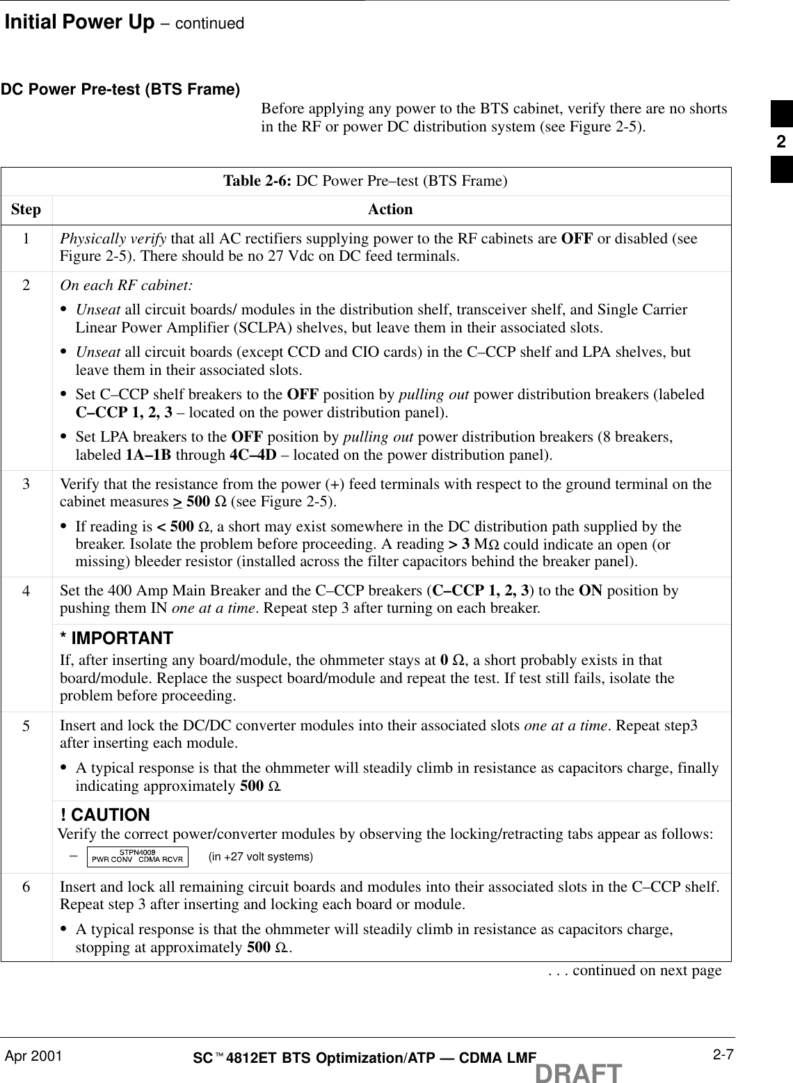
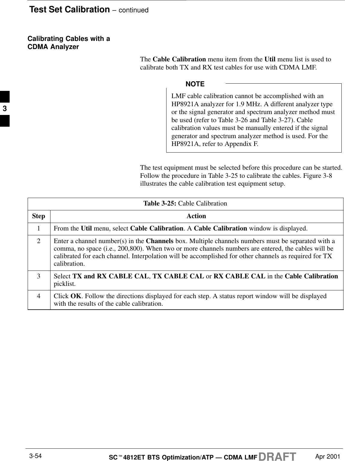
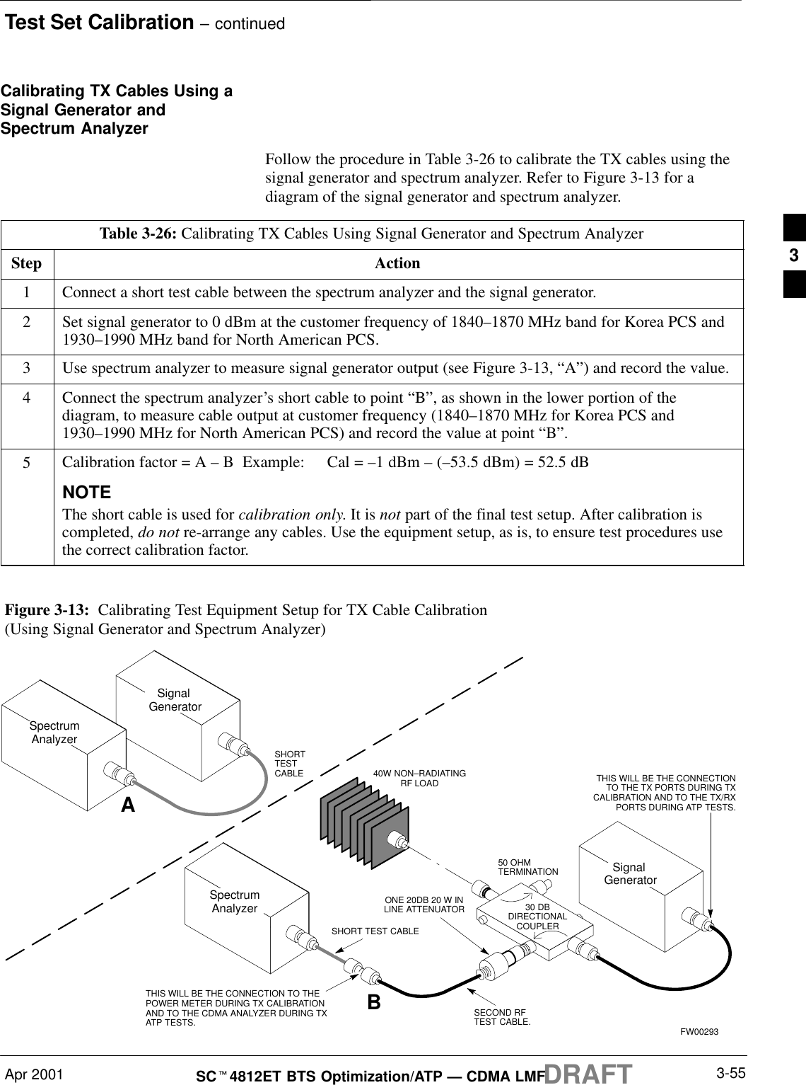
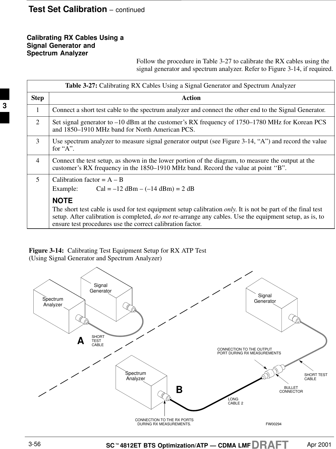
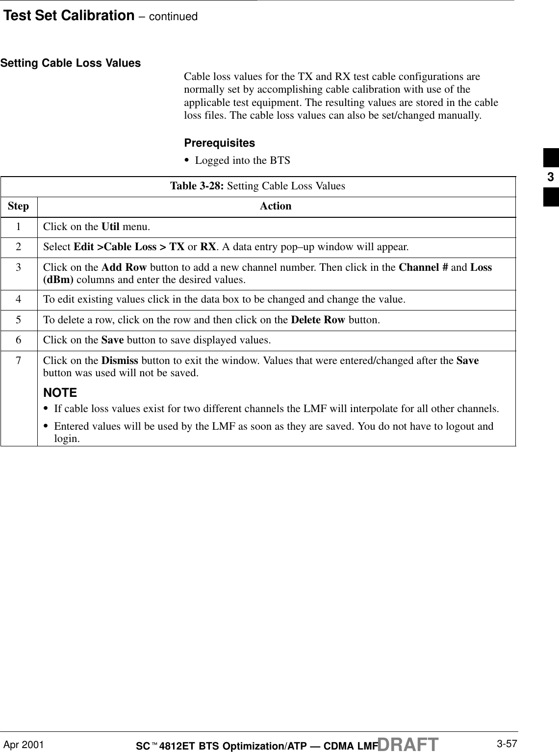
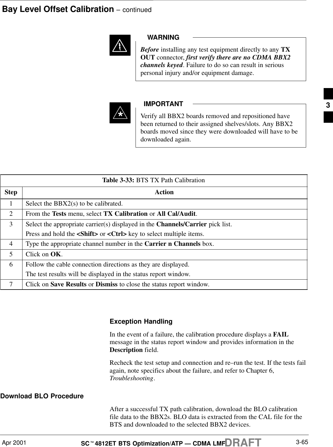
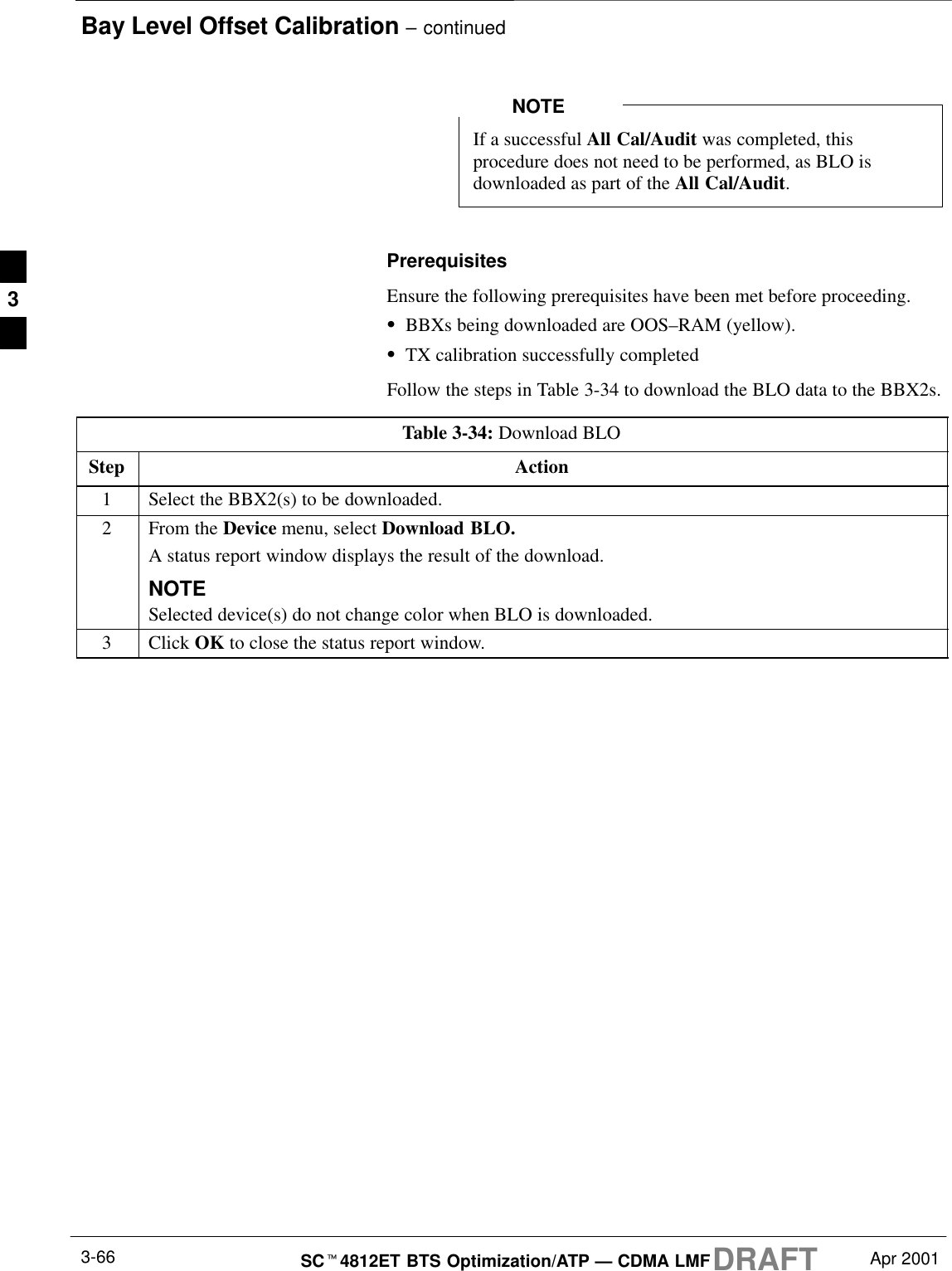
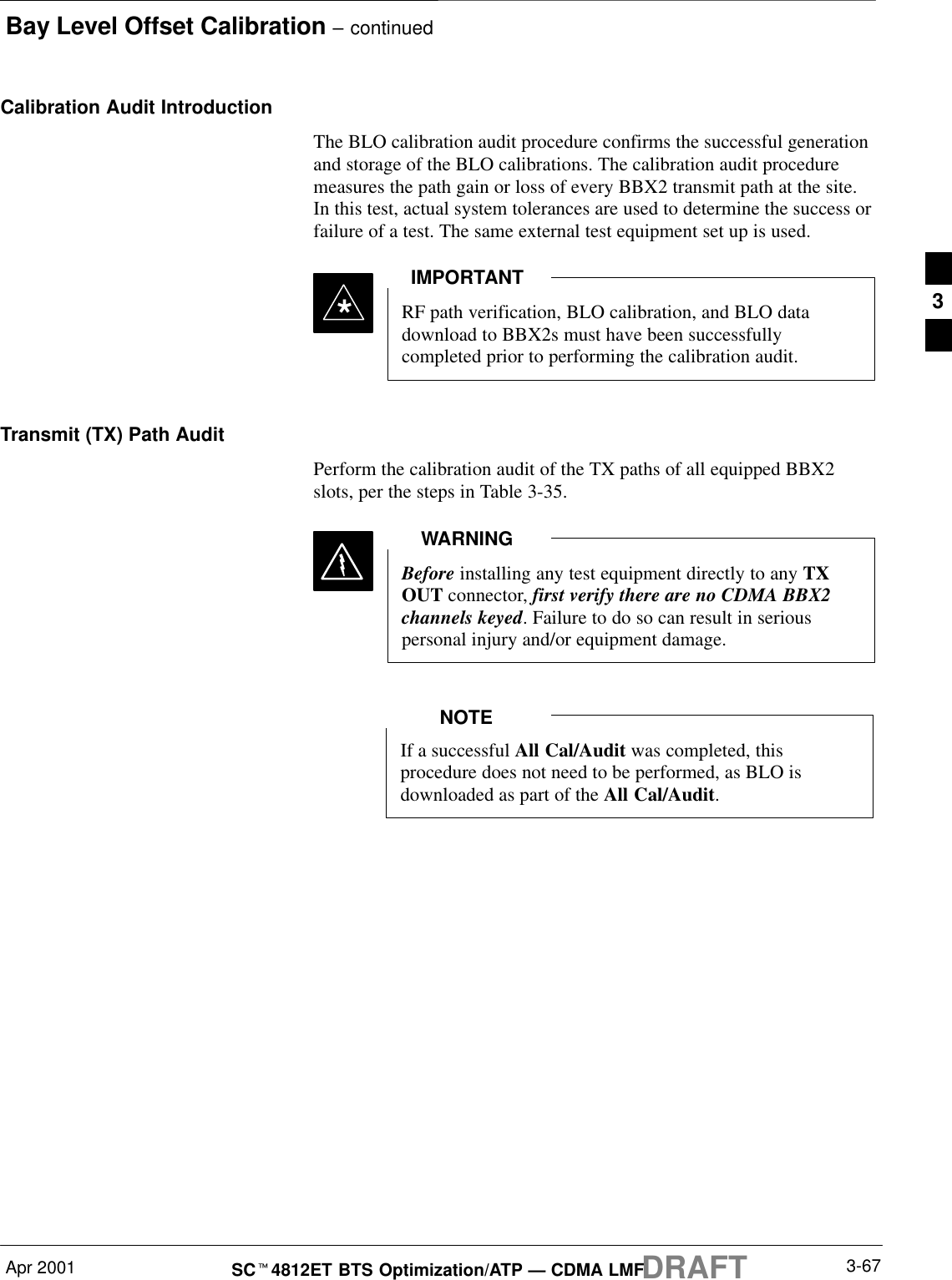
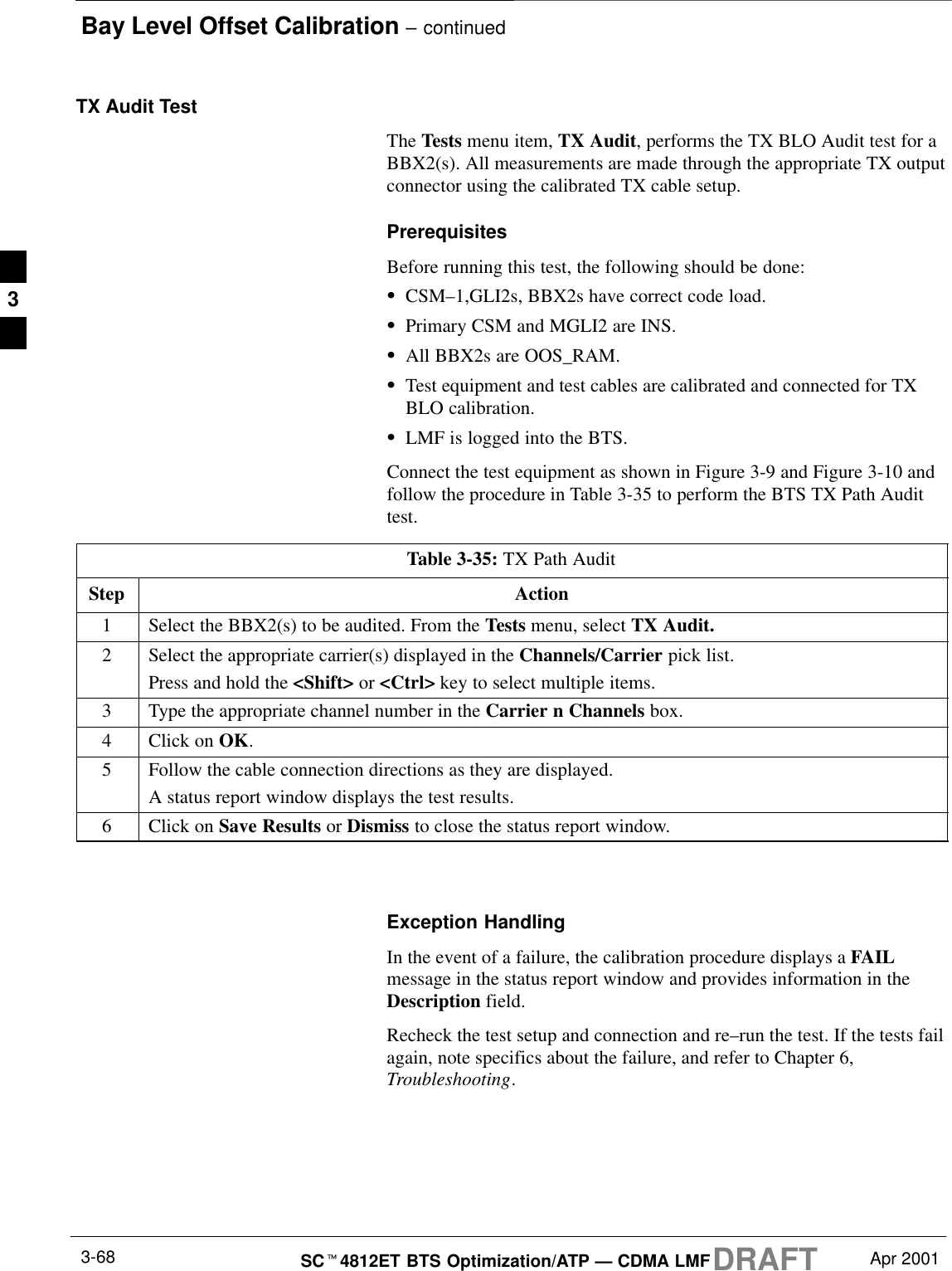
Initial Power UpApr 2001 2-3SCt4812ET BTS Optimization/ATP — CDMA LMFDRAFTIntroductionThe following information is used to check for any electrical shortcircuits and to verify the operation and tolerances of the cellsite and BTSpower supply units before applying power for the first time. It containsinstructional information on the initial proper power up procedures forthe SC 4812ET power cabinet and RF cabinet. Also presented are teststo be preformed on the power cabinet. Please pay attention to allcautions and warning statements in order to prevent accidental injury topersonnel.Required ToolsThe following tools are used in the procedures.SDC current clamp (600 Amp capability with jaw size to accommodate2/0 cable).SHot Air Gun – (optional for part of the Alarm Verification)SDigital Multimeter (DMM)Cabling InspectionUsing the site-specific documentation generated by Motorola SystemsEngineering, verify that the following cable systems are properlyconnected:SReceive RF cabling – up to 12 RX cablesSTransmit RF cabling – up to six TX cablesFor positive power applications (+27 V):SThe positive power cable is red.SThe negative power cable is black. (The black powercable is at ground potential.)IMPORTANT*Initial Inspection and SetupEnsure all battery breakers for unused battery positions areopen (pulled out) during any part of the power up process,and remain in the off position when leaving the site.CAUTIONTable 2-2: Initial Inspection and SetupStep Action1Verify that ALL AC and DC breakers are turned OFF in both the Power and RF cabinets. Verify thatthe DC power cables between the Power and RF cabinets are connected with the correct polarity2The RED cables  connect to the uppermost three (3) terminals (marked +) in both cabinets. Confirmthat the split phase 240/120 AC supply is correctly connected to the AC load center input.2
Initial Power Up – continuedDRAFTSCt4812ET BTS Optimization/ATP — CDMA LMF Apr 20012-4Failure to connect the proper AC feed will damage thesurge protection module inside the AC load center.CAUTIONPower Up SequenceThe first task in the power up sequence is to apply AC power to thePower cabinet. Once power is applied a series of AC Voltagemeasurements is required.Table 2-3: AC Voltage MeasurementsStep Action1Measure the AC voltages connected to the AC load center (access the terminals from the rear of thecabinet after removing the AC load center rear panel). See Figure 2-2.2Measure the AC voltage from terminal L1 to neutral. This voltage should be in the range of nominally115 to 120 V AC.3Measure the AC voltage from terminal L1 to ground. This voltage should be in the range of nominally115 to 120 V AC.4Measure the AC voltage from terminal L2 to neutral. This voltage should be in the range of nominally115 to 120 V AC.5Measure the AC voltage from terminal L2 to ground. This voltage should be in the range of nominally115 to 120 V AC.6Measure L1 – L2 – should be from  208 to 240 V AC. If the AC voltages are in excess of 120 V (or exceed200 V) when measuring between terminals L1 or L2 toneutral or  ground, STOP and Do Not proceed until thecause of the higher voltages are determined. The powercabinet WILL be damaged if the Main breaker is turnedon with excessive voltage on the inputs.CAUTION2
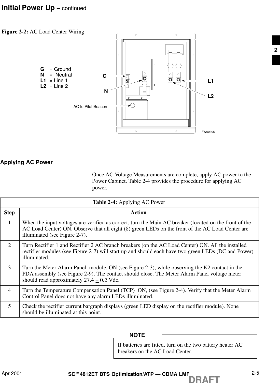
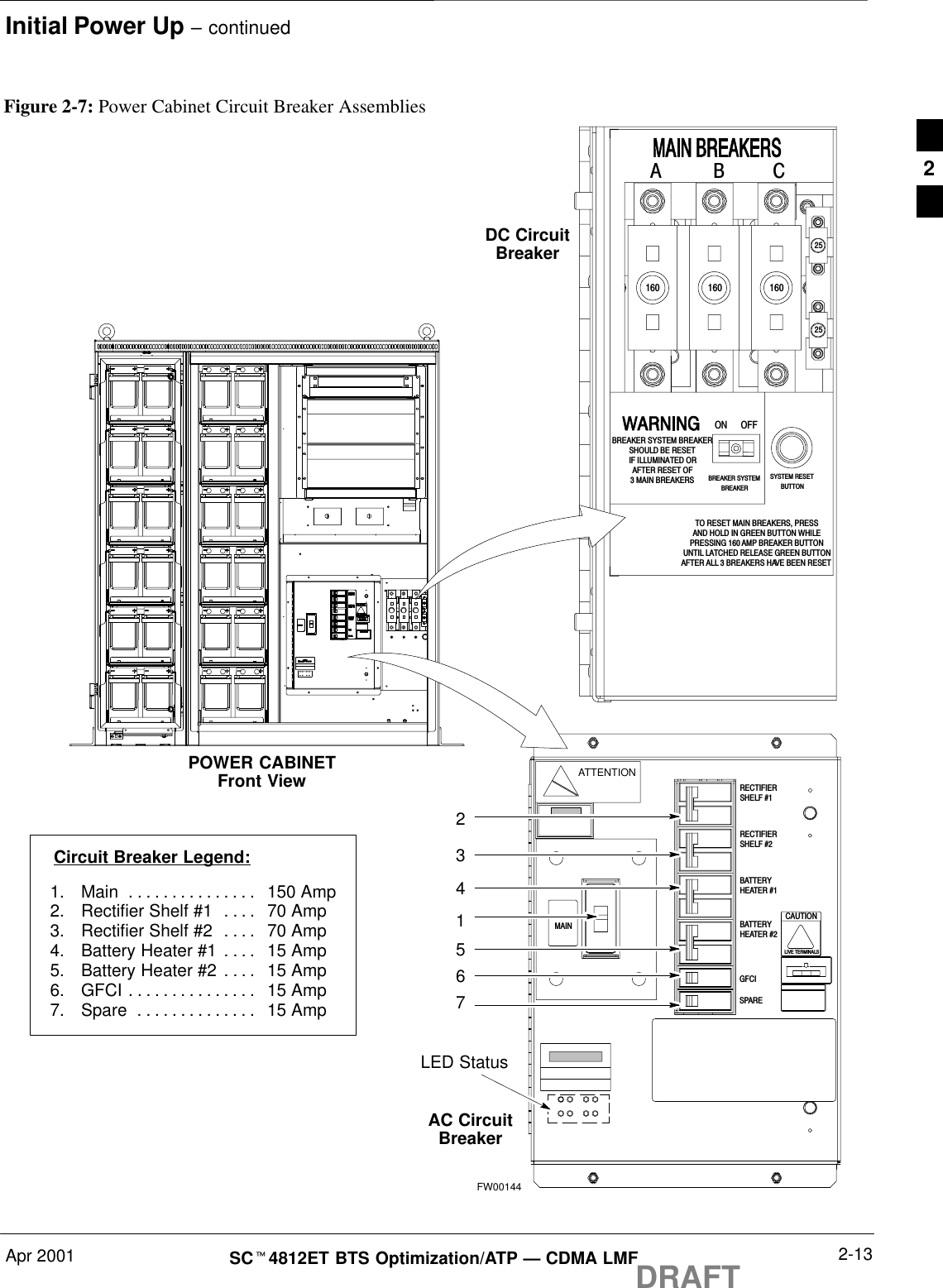
Initial Power Up – continuedApr 2001 2-5SCt4812ET BTS Optimization/ATP — CDMA LMFDRAFTFigure 2-2: AC Load Center Wiring   G= GroundN  =  NeutralL1 = Line 1L2 = Line 2GNAC to Pilot BeaconL2L1FW00305Applying AC PowerOnce AC Voltage Measurements are complete, apply AC power to thePower Cabinet. Table 2-4 provides the procedure for applying ACpower.Table 2-4: Applying AC PowerStep Action1When the input voltages are verified as correct, turn the Main AC breaker (located on the front of theAC Load Center) ON. Observe that all eight (8) green LEDs on the front of the AC Load Center areilluminated (see Figure 2-7).2Turn Rectifier 1 and Rectifier 2 AC branch breakers (on the AC Load Center) ON. All the installedrectifier modules (see Figure 2-7) will start up and should each have two green LEDs (DC and Power)illuminated.3Turn the Meter Alarm Panel  module, ON (see Figure 2-3), while observing the K2 contact in thePDA assembly (see Figure 2-9). The contact should close. The Meter Alarm Panel voltage metershould read approximately 27.4 + 0.2 Vdc.4Turn the Temperature Compensation Panel (TCP)  ON, (see Figure 2-4). Verify that the Meter AlarmControl Panel does not have any alarm LEDs illuminated.5Check the rectifier current bargraph displays (green LED display on the rectifier module). Noneshould be illuminated at this point.If batteries are fitted, turn on the two battery heater ACbreakers on the AC Load Center.NOTE2
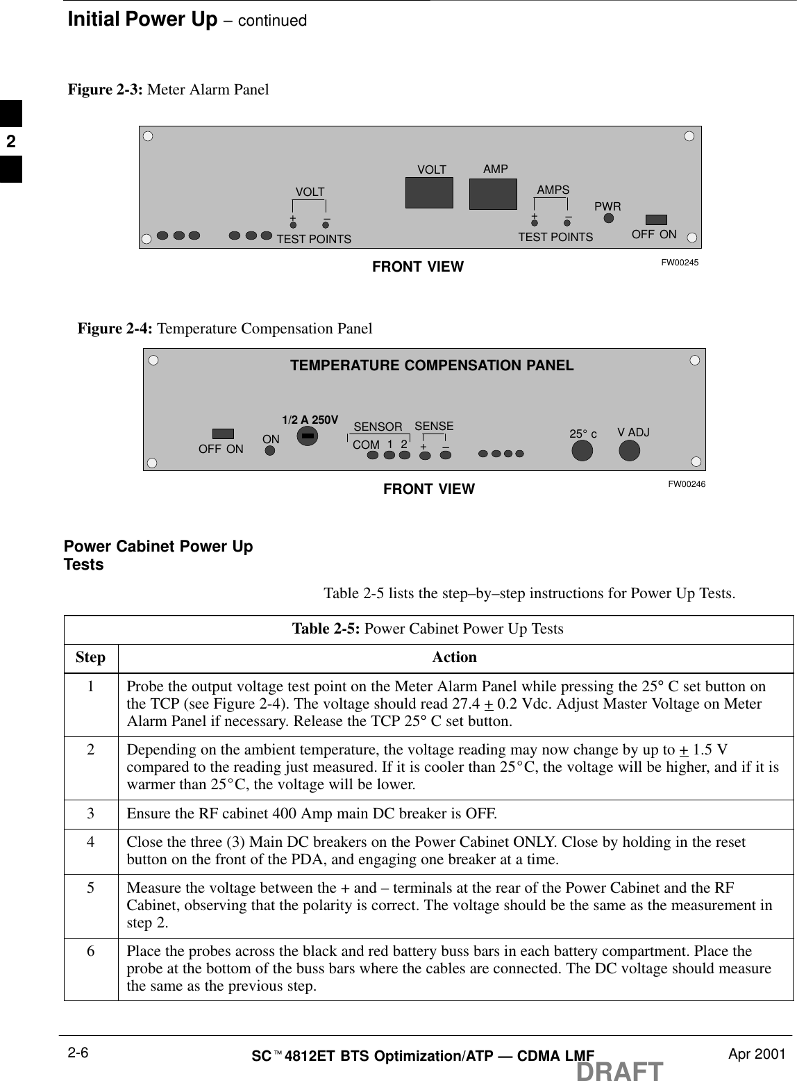
Initial Power Up – continuedDRAFTSCt4812ET BTS Optimization/ATP — CDMA LMF Apr 20012-6Figure 2-3: Meter Alarm PanelOFFVOLTVOLT–+TEST POINTSAMPS–+TEST POINTSAMPPWRONFRONT VIEW FW00245Figure 2-4: Temperature Compensation PanelOFFV ADJSENSOR 25_ cSENSE–+COMONONFRONT VIEW1/2 A 250V12TEMPERATURE COMPENSATION PANELFW00246Power Cabinet Power UpTestsTable 2-5 lists the step–by–step instructions for Power Up Tests.Table 2-5: Power Cabinet Power Up TestsStep Action1Probe the output voltage test point on the Meter Alarm Panel while pressing the 25° C set button onthe TCP (see Figure 2-4). The voltage should read 27.4 + 0.2 Vdc. Adjust Master Voltage on MeterAlarm Panel if necessary. Release the TCP 25° C set button.2Depending on the ambient temperature, the voltage reading may now change by up to + 1.5 Vcompared to the reading just measured. If it is cooler than 25_C, the voltage will be higher, and if it iswarmer than 25_C, the voltage will be lower.3Ensure the RF cabinet 400 Amp main DC breaker is OFF.4Close the three (3) Main DC breakers on the Power Cabinet ONLY. Close by holding in the resetbutton on the front of the PDA, and engaging one breaker at a time.5Measure the voltage between the + and – terminals at the rear of the Power Cabinet and the RFCabinet, observing that the polarity is correct. The voltage should be the same as the measurement instep 2.6Place the probes across the black and red battery buss bars in each battery compartment. Place theprobe at the bottom of the buss bars where the cables are connected. The DC voltage should measurethe same as the previous step. 2
Initial Power Up – continuedApr 2001 2-7SCt4812ET BTS Optimization/ATP — CDMA LMFDRAFTDC Power Pre-test (BTS Frame) Before applying any power to the BTS cabinet, verify there are no shortsin the RF or power DC distribution system (see Figure 2-5).Table 2-6: DC Power Pre–test (BTS Frame)Step Action1Physically verify that all AC rectifiers supplying power to the RF cabinets are OFF or disabled (seeFigure 2-5). There should be no 27 Vdc on DC feed terminals.2On each RF cabinet:SUnseat all circuit boards/ modules in the distribution shelf, transceiver shelf, and Single CarrierLinear Power Amplifier (SCLPA) shelves, but leave them in their associated slots.SUnseat all circuit boards (except CCD and CIO cards) in the C–CCP shelf and LPA shelves, butleave them in their associated slots.SSet C–CCP shelf breakers to the OFF position by pulling out power distribution breakers (labeledC–CCP 1, 2, 3 – located on the power distribution panel).SSet LPA breakers to the OFF position by pulling out power distribution breakers (8 breakers,labeled 1A–1B through 4C–4D – located on the power distribution panel).3Verify that the resistance from the power (+) feed terminals with respect to the ground terminal on thecabinet measures > 500 Ω (see Figure 2-5).SIf reading is < 500 Ω, a short may exist somewhere in the DC distribution path supplied by thebreaker. Isolate the problem before proceeding. A reading > 3 MΩ could indicate an open (ormissing) bleeder resistor (installed across the filter capacitors behind the breaker panel).4Set the 400 Amp Main Breaker and the C–CCP breakers (C–CCP 1, 2, 3) to the ON position bypushing them IN one at a time. Repeat step 3 after turning on each breaker.* IMPORTANTIf, after inserting any board/module, the ohmmeter stays at 0 Ω, a short probably exists in thatboard/module. Replace the suspect board/module and repeat the test. If test still fails, isolate theproblem before proceeding.5Insert and lock the DC/DC converter modules into their associated slots one at a time. Repeat step3after inserting each module.SA typical response is that the ohmmeter will steadily climb in resistance as capacitors charge, finallyindicating approximately 500 Ω.! CAUTIONVerify the correct power/converter modules by observing the locking/retracting tabs appear as follows:–  (in +27 volt systems)6Insert and lock all remaining circuit boards and modules into their associated slots in the C–CCP shelf.Repeat step 3 after inserting and locking each board or module.SA typical response is that the ohmmeter will steadily climb in resistance as capacitors charge,stopping at approximately 500 Ω... . . continued on next page2
Initial Power Up – continuedDRAFTSCt4812ET BTS Optimization/ATP — CDMA LMF Apr 20012-8Table 2-6: DC Power Pre–test (BTS Frame)Step Action7Set the 8 LPA breakers ON by pushing them IN one at a time. Repeat step 3 after turning on eachbreaker.SA typical response is that the ohmmeter will steadily climb in resistance as capacitors charge,stopping at approximately 500 Ω..8Seat all LPA and associated LPA fan modules into their associated slots in the shelves one at a time.Repeat step 3 after seating each LPA  and associated LPA fan module.SA typical response is that the ohmmeter will steadily climb in resistance as capacitors charge,stopping at approximately 500 Ω..9Seat the Heat Exchanger, ETIB, and Options breakers one at a time. Repeat step 3. RF Cabinet Power UpTable 2-7 covers the procedures for properly powering up the RFCabinet.Table 2-7: RF Cabinet Power UpStep Action1Ensure the 400 Amp Main DC breaker and all other breakers in the RF Cabinet are OFF.2Proceed to the DC Power Pre–test (BTS Frame) sequence (see Table 2-6) (for initial power–up asrequired).3Ensure the power cabinet is turned on  (see Table 2-5). Verify that 27 volts is applied to the terminalson the back of the RF cabinet.4Engage the main DC circuit breaker on the RF cabinet (see Figure 2-5).5On each RF cabinet:SSet C–CCP shelf breakers to the ON position by pushing them in one at a time (labeledC–CCP 1, 2, 3 – located on the power distribution panel).SSet LPA breakers to the ON position by pushing them in one at a time  (8 breakers, labeled 1A–1Bthrough 4C–4D – located on the power distribution panel).SSet the two heat exchanger breakers to the ON position by pushing them in one at a time.SSet the ETIB breaker to the ON position by pushing it in.SSet the OPTION breaker  to the ON position by pushing it in.. . . continued on next page2
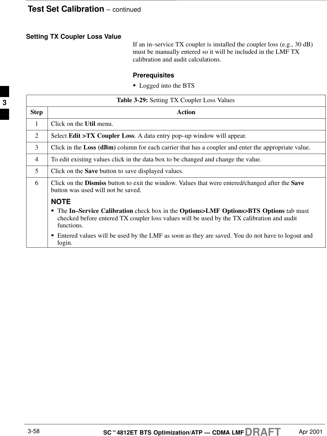
Initial Power Up – continuedApr 2001 2-9SCt4812ET BTS Optimization/ATP — CDMA LMFDRAFTTable 2-7: RF Cabinet Power UpStep Action6Measure the voltage drop between the Power Cabinet meter test point and the 27 V buss bar inside theRF Cabinet PDA while the RF Cabinet is transmitting.NOTEFor a three (3) sector carrier system, the voltage drop should be less than 0.2 V.For a twelve (12) sector carrier system, the voltage drop should be less than 0.3 V.7Using a DC current probe, measure the current in each of the six (6) DC cables that are connectedbetween the RF and Power Cabinet. The DC current measured should be approximately the same. Ifthere is a wide variation between one cable and the others (>20 A), check the tightness of theconnections (torque settings) at each end of the cable. RF CABINET(Rear View)27V27V RetFigure 2-5: RF Cabinet Circuit Breaker Panel and 27V DC Terminal LocationsMAIN BREAKER 5 RU RACKSPACESC 4812ET BTS RF Cabinet(Front View)4003030303030303030505050LPA1B1D2B2D3B3D4B4D1A1C2A2C3A3C4A4CPS1PS2PS3CCCP2525ETIBOPTION1015HEAT EXCHANGERCAUTIONSHUT OFF BOTH BREAKERSONLY  DURING HEAT EXCHANGERMAINTENANCE OR REPAIRLPABLOWERSPUSH BUTTONTO RESETLPA BLOWERSFW00307I/O Plate + and – DC FeedTerminals (Back Panel of RFCabinet)2
Initial Power Up – continuedDRAFTSCt4812ET BTS Optimization/ATP — CDMA LMF Apr 20012-10Battery Charge Test(Connected Batteries)Table 2-8 lists the step–by–step instructions for testing the batteries.Table 2-8: Battery Charge Test (Connected Batteries)Step Action1Close the battery compartment breakers for connected batteries ONLY. This process should becompleted quickly to avoid individual battery strings with excess charge currentNOTEIf the batteries are sufficiently discharged, the battery circuit breakers may not engage individuallydue to the surge current. If this condition is observed, turn off the Meter Alarm Panel power switch,and then engage all the connected battery circuit breakers, the Meter Alarm Panel  power switchshould then be turned ON.2Using the DC current probe, measure the current in each of the battery string connections to the bussbars in each battery cabinet. The charge current may initially be high but should quickly reduce in afew minutes if the batteries have a typical new battery charge level.3The current in each string should be approximately equal  (+ 5 A).4The bargraph meters on the rectifier modules can be used as a rough estimate of  the total batterycharge current. Each rectifier module has eight (8) LEDs to represent the output current. Eachilluminated LED indicates that approximately 12.5% (1/8 or 8.75 A) of the rectifiers maximum (70 A)current is flowing.EXAMPLE:Question: A system fitted with three (3) rectifier modules each have three bargraph LEDsilluminated. What is the total output current into the batteries?Answer: Each bargraph is approximately indicating 12.5% of 70 A, therefore, 3 X 8.75 equals26.25 A. As there are three rectifiers, the total charge current is equal to (3 X 26.25 A) 78.75 A.This charge current calculation only applies at this part of the start up procedure, when the RF Cabinetis not powered on, and the power cabinet heat exchanger is turned off.5Allow a few minutes to ensure that the battery charge current stabilizes before taking any furtheraction. Recheck the battery current in each string. If the batteries had a reasonable charge, the currentin each string should reduce to less than 5 A.6Recheck the DC output voltage. It should remain the same as measured in step 4 of the Power UpTest.NOTEIf discharged batteries are installed, all bargraphs may be illuminated on the rectifiers during thecharge test. This indicates that the rectifiers are at full capacity and are rapidly charging the batteries.It is recommended in this case that the batteries are allowed to charge and stabilize as in the abovestep before commissioning the site. This could take several hours. Battery Discharge TestPerform the test procedure in Table 2-9 only when the battery current isless than 5 A per string. Refer to Table 2-8 on the procedures forchecking current levels.2
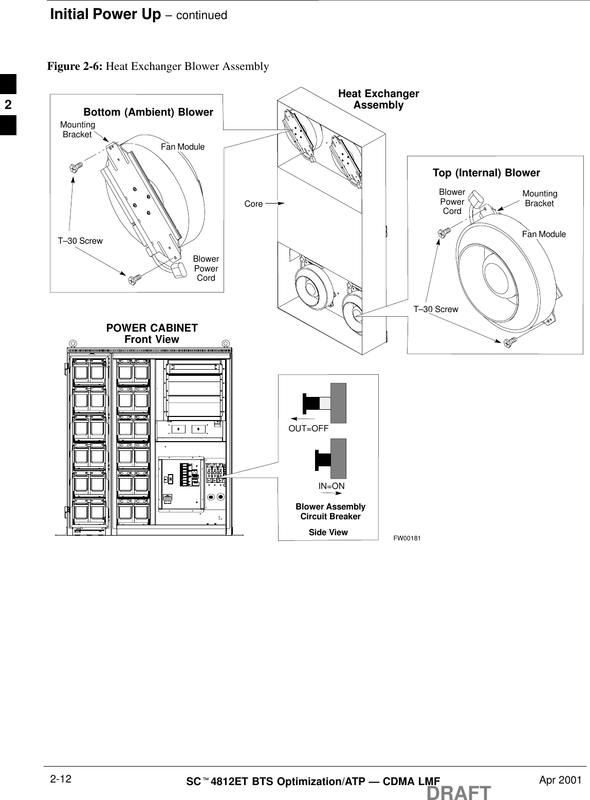
Initial Power Up – continuedApr 2001 2-11SCt4812ET BTS Optimization/ATP — CDMA LMFDRAFTTable 2-9: Battery Discharge TestStep Action1Turn the battery test switch on the Meter Alarm Panel, ON (see Figure 2-3). The rectifier outputvoltage and current should decrease by approximately 10% as the batteries assume the load. Alarmsfor the Meter Alarm Panel may occur.2Measure the individual battery string current using the DC current probe. The battery dischargecurrent in each string should be approximately the same (within + 5 A).3Turn Battery Test Switch OFF.Failure to turn OFF the Battery Test Switch before leavingthe site, will result in low battery capacity and reducebattery life.CAUTIONHeat Exchanger Power UpTable 2-10: Heat Exchanger Power UpStep Action1Turn the Power Cabinet Heat Exchanger breakers ON (seeFigure 2-6 for breaker location).2The Heat Exchanger will now go into a 5 minute test sequence. Ensure that the internal and externalfans are operating. Place a hand on the internal and external Heat Exchanger grills to feel for air draft.2
Initial Power Up – continuedDRAFTSCt4812ET BTS Optimization/ATP — CDMA LMF Apr 20012-12CoreHeat ExchangerAssemblyPOWER CABINETFront ViewOUT=OFFIN=ONBlower AssemblyCircuit BreakerFW00181Side ViewMountingBracketT–30 ScrewTop (Internal) BlowerFan ModuleBlowerPowerCordBlowerPowerCordBottom (Ambient) BlowerFan ModuleT–30 ScrewMountingBracketFigure 2-6: Heat Exchanger Blower Assembly2
Initial Power Up – continuedApr 2001 2-13SCt4812ET BTS Optimization/ATP — CDMA LMFDRAFTLED StatusFigure 2-7: Power Cabinet Circuit Breaker AssembliesA B CBREAKER SYSTEM BREAKERSHOULD BE RESETIF ILLUMINATED ORAFTER RESET OF3 MAIN BREAKERSTO RESET MAIN BREAKERS, PRESSAND HOLD IN GREEN BUTTON WHILEPRESSING 160 AMP BREAKER BUTTONUNTIL LATCHED RELEASE GREEN BUTTONAFTER ALL 3 BREAKERS HAVE BEEN RESETON OFFBREAKER SYSTEMBREAKERSYSTEM RESETBUTTONFW00144POWER CABINETFront ViewAC CircuitBreakerDC CircuitBreaker160 160 1602525Circuit Breaker Legend:1. Main 150 Amp. . . . . . . . . . . . . . . 2. Rectifier Shelf #1 70 Amp. . . . 3. Rectifier Shelf #2 70 Amp. . . . 4. Battery Heater #1 15 Amp. . . . 5. Battery Heater #2 15 Amp. . . . 6. GFCI 15 Amp. . . . . . . . . . . . . . . 7. Spare 15 Amp. . . . . . . . . . . . . . RECTIFIERSHELF #1RECTIFIERSHELF #2BATTERYHEATER #1GFCISPAREBATTERYHEATER #2CAUTIONLIVE TERMINALS2345617ATTENTIONMAIN2
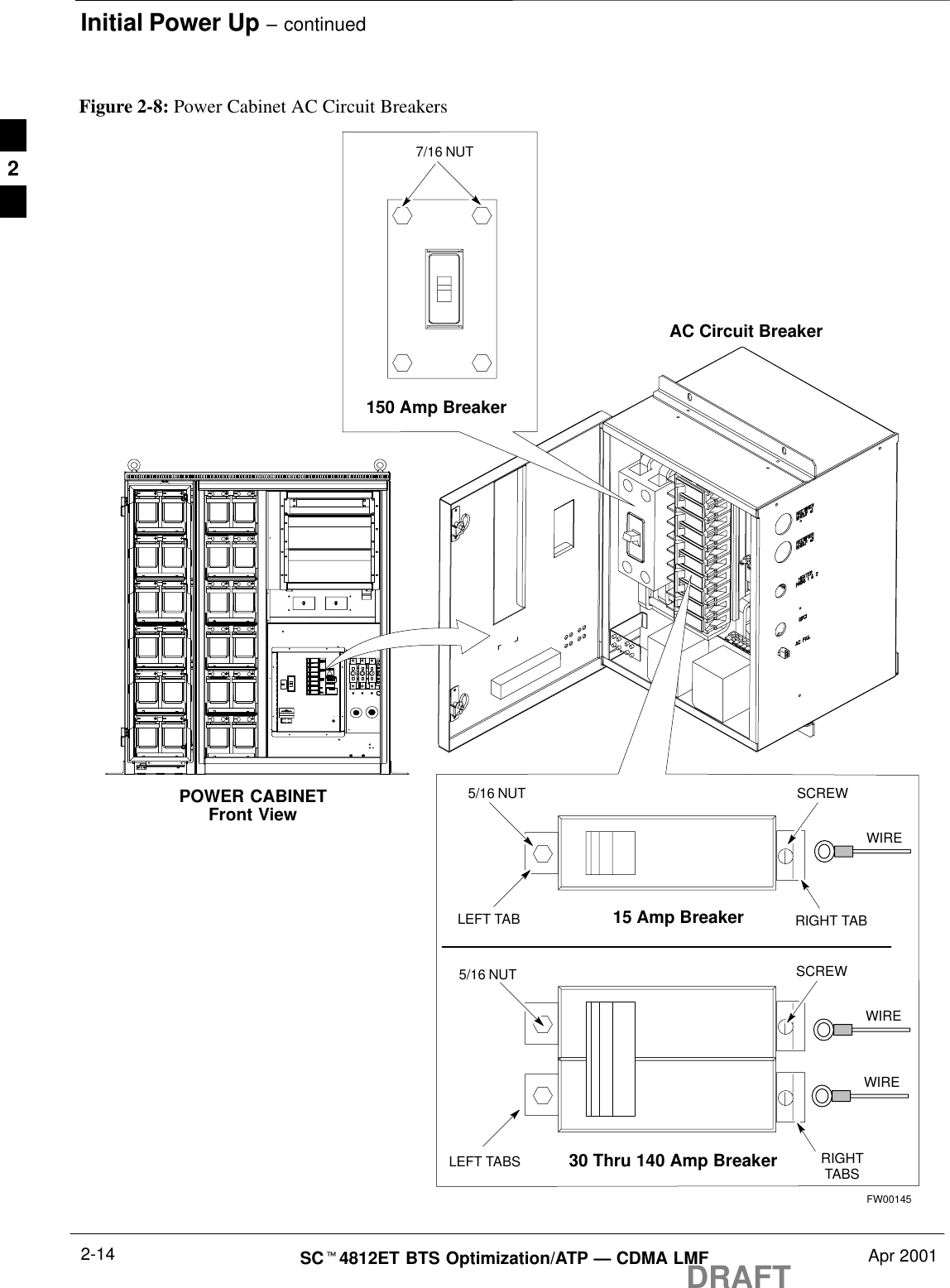
Initial Power Up – continuedDRAFTSCt4812ET BTS Optimization/ATP — CDMA LMF Apr 20012-1415 Amp Breaker5/16 NUTLEFT TABSCREWWIRERIGHT TAB30 Thru 140 Amp BreakerFigure 2-8: Power Cabinet AC Circuit Breakers150 Amp Breaker7/16 NUTPOWER CABINETFront ViewAC Circuit BreakerFW00145SCREWWIRERIGHTTABSWIRE5/16 NUTLEFT TABS2
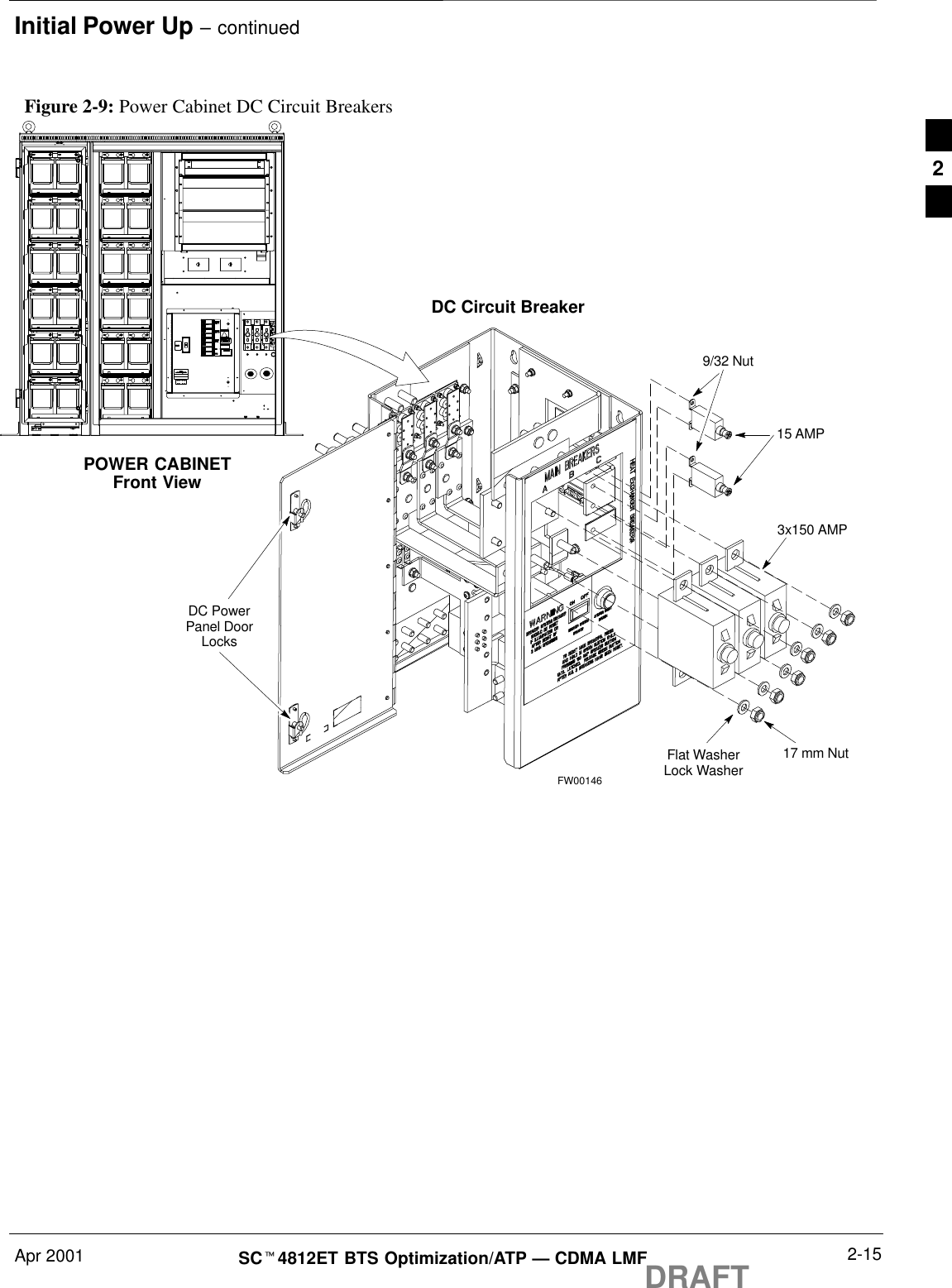
Initial Power Up – continuedApr 2001 2-15SCt4812ET BTS Optimization/ATP — CDMA LMFDRAFTFigure 2-9: Power Cabinet DC Circuit BreakersPOWER CABINETFront ViewDC Circuit BreakerFW0014615 AMP3x150 AMPFlat WasherLock Washer 17 mm NutDC PowerPanel DoorLocks9/32 Nut2
Initial Power Up – continuedDRAFTSCt4812ET BTS Optimization/ATP — CDMA LMF Apr 20012-16Notes2
Optimization/Calibration – IntroductionApr 2001 3-1SCt4812ET BTS Optimization/ATP — CDMA LMFDRAFTIntroductionThis chapter provides procedures for downloading system operatingsoftware, set up of the supported test equipment, CSM referenceverification/optimization, and transmit/receive path verification.Before using the LMF, use an editor to view the”CAVEATS” section in the ”readme.txt” file in the c:\wlmffolder for any applicable information.IMPORTANT*Optimization ProcessAfter a BTS is physically installed and the preliminary operations(power up) have been completed, the CDMA LMF is used to calibrateand optimize the BTS. The basic optimization process can beaccomplished as follows:SDownload MGLI2–1 with code and data and then enable MGLI2–1.SUse the status function and verify that all of the installed devices ofthe following types respond with status information: CSM2, BBX2,GLI2, and MCC (and TSU if RFDS is installed). If a device isinstalled and powered up but is not responding and is colored gray inthe BTS display, the device is not listed in the CDF file. The CDF filewill have to be corrected before the device can be accessed by CDMALMF.SDownload code and data to all devices of the following types:– CSM2– BBX–GLI2 (other than MGLI2–1)– MCCSDownload the RFDS TSIC (if installed).SVerify the operation of the GPS and HSO signals.SEnable the following devices (in the order listed):–Secondary CSM (slot 2)–Primary CSM (slot 1)–All MCCsSConnect the required test equipment for a full optimization.SSelect the test equipment.SCalibrate the TX and RX test cables if they have not previously beencalibrated using the CDMA LMF that is going to be used for theoptimization/calibration. The cable calibration values can also beentered manually. . . . continued on next page3
Optimization/Calibration – Introduction – continuedDRAFTSCt4812ET BTS Optimization/ATP — CDMA LMF Apr 20013-2SSelect all of the BBXs and all of the MCCs and use the fulloptimization function. The full optimization function performs TXcalibration, BLO download, TX audit, all TX tests, and all RX testsfor all selected devices.SIf the TX calibration fails, repeat the full optimization for any failedpaths.SIf the TX calibration fails again, correct the problem that caused thefailure and repeat the full optimization for the failed path.SIf the TX calibration and audit portion of the full optimization passesfor a path but some of the TX or RX tests fail, correct the problem thatcaused the failure and run the individual tests as required until all TXand RX tests have passed for all paths.Cell–site TypesSites are configured as Omni/Omni or Sector/Sector (TX/RX). Each typehas unique characteristics and must be optimized accordingly.Cell–site Data File The CDF includes the following information:SDownload instructions and protocolSSite specific equipage informationSC–CCP shelf allocation plan–BBX2 equipage (based on cell–site type) including redundancy–CSM equipage including redundancy–MCC (MCC24E, MCC8E or MCC–1X) channel element allocationplan. This plan indicates how the C–CCP shelf is configured, andhow the paging, synchronization, traffic, and access channelelements (and associated gain values) are assigned among the (up to12) MCCs in the shelf.SCSM equipage including redundancySEffective Rated Power (ERP) table for all TX channels to antennasrespectively.  Motorola System Engineering specifies the ERP of atransmit antenna based on site geography, antenna placement, andgovernment regulations. Working from this ERP requirement, theantenna gain, (dependent on the units of measurement specified) andantenna feed line loss can be combined to determine the requiredpower at the top of the BTS frame.  The corresponding BBX2 outputlevel required to achieve that power level on any channel/sector canalso be determined.Refer to the CDMA LMF Operator’s Guide, 68P64114A78,for additional information on the layout of the LMFdirectory structure (including CDF file locations andformats).NOTE3
Optimization/Calibration – Introduction – continuedApr 2001 3-3SCt4812ET BTS Optimization/ATP — CDMA LMFDRAFTBTS System SoftwareDownloadBTS system software must be successfully downloaded to the BTSprocessor boards before optimization can be performed. BTS operatingcode is loaded from the LMF computer terminal.Before using the LMF for optimization/ATP, the correctbts–#.cdf and cbsc–#.cdf files for the BTS must beobtained from the CBSC and put in a bts–# folder in theLMF. Failure to use the correct CDF files can cause wrongresults. Failure to use the correct CDF files to log into alive (traffic carrying) site can shut down the site.IMPORTANT*The CDF is normally obtained from the CBSC on a DOS formatteddiskette, or through a file transfer protocol (ftp) if the LMF computer hasftp capability. Refer to the CDMA LMF Operator’s Guide,68P64114A78, or the LMF Help screen, for more information.Site Equipage VerificationIf you have not already done so, use an editor to view the CDF, andreview the site documentation. Verify the site engineering equipage datain the CDF to the actual site hardware.Always wear a conductive, high impedance wrist strapwhile handling any circuit card/module to prevent damageby ESD. Extreme care should be taken during the removaland installation of any card/module. After removal, thecard/module should be placed on a conductive surface orback into the anti–static bag in which it was shipped.CAUTION3
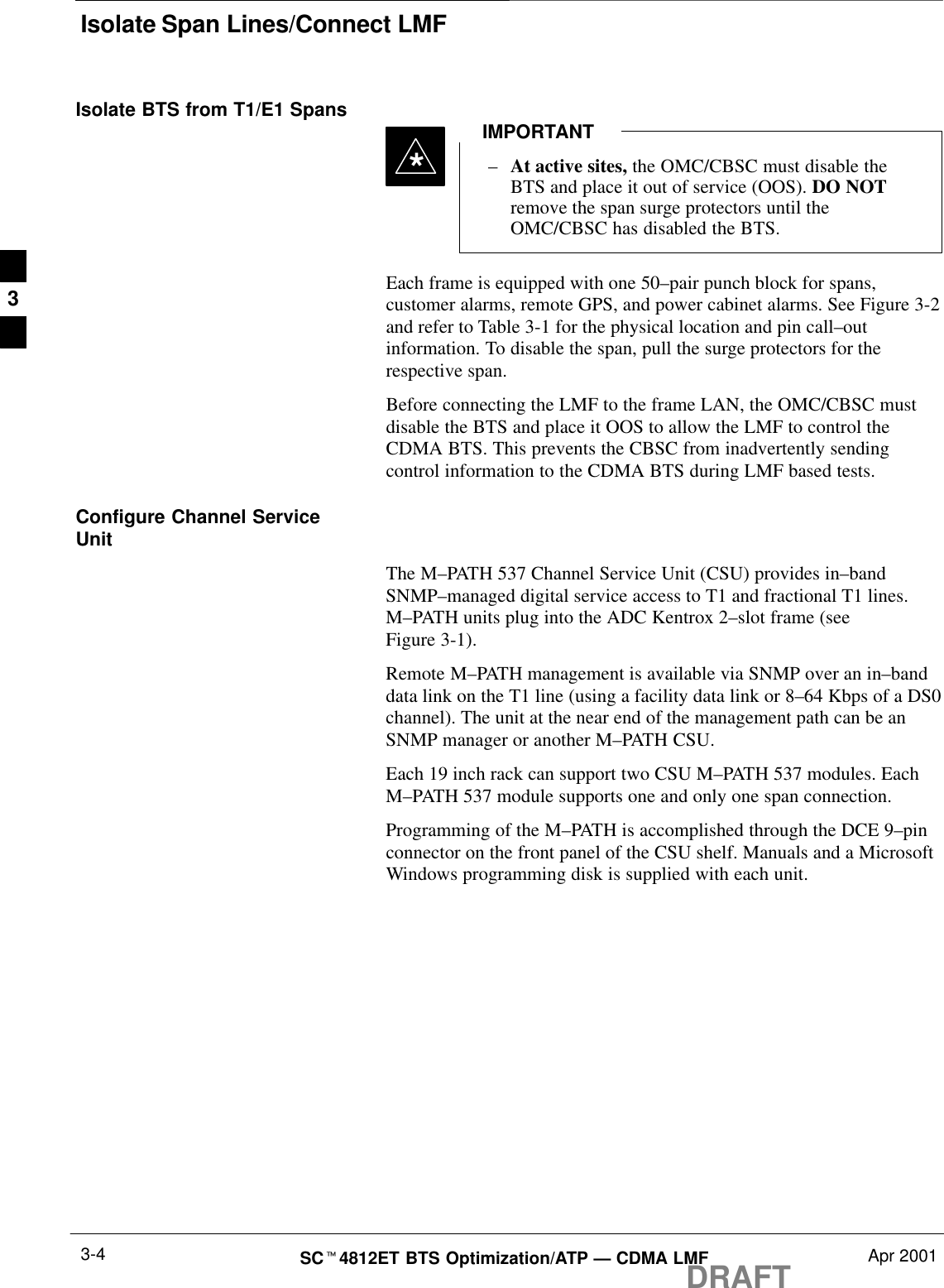
Isolate Span Lines/Connect LMFDRAFTSCt4812ET BTS Optimization/ATP — CDMA LMF Apr 20013-4Isolate BTS from T1/E1 Spans–At active sites, the OMC/CBSC must disable theBTS and place it out of service (OOS). DO NOTremove the span surge protectors until theOMC/CBSC has disabled the BTS.IMPORTANT*Each frame is equipped with one 50–pair punch block for spans,customer alarms, remote GPS, and power cabinet alarms. See Figure 3-2and refer to Table 3-1 for the physical location and pin call–outinformation. To disable the span, pull the surge protectors for therespective span.Before connecting the LMF to the frame LAN, the OMC/CBSC mustdisable the BTS and place it OOS to allow the LMF to control theCDMA BTS. This prevents the CBSC from inadvertently sendingcontrol information to the CDMA BTS during LMF based tests.Configure Channel ServiceUnitThe M–PATH 537 Channel Service Unit (CSU) provides in–bandSNMP–managed digital service access to T1 and fractional T1 lines.M–PATH units plug into the ADC Kentrox 2–slot frame (seeFigure 3-1).Remote M–PATH management is available via SNMP over an in–banddata link on the T1 line (using a facility data link or 8–64 Kbps of a DS0channel). The unit at the near end of the management path can be anSNMP manager or another M–PATH CSU.Each 19 inch rack can support two CSU M–PATH 537 modules. EachM–PATH 537 module supports one and only one span connection.Programming of the M–PATH is accomplished through the DCE 9–pinconnector on the front panel of the CSU shelf. Manuals and a MicrosoftWindows programming disk is supplied with each unit.3
Isolate Span Lines/Connect LMF – continuedApr 2001 3-5SCt4812ET BTS Optimization/ATP — CDMA LMFDRAFTSetting the Control PortWhichever control port is chosen, it must first be set up so the controlport switches match the communication parameters being used by thecontrol device. If using the rear–panel DTE control port, set theshelf–address switch SA5 to “up” (leave the switch down for therear–panel DCE control port).For more information, refer to the Kentrox Installation Guide, manualnumber 65–77538001 which is provided with each CSU.Plug one of the cables listed below into the Control Port connectors:Part Number Description of Cable01–95006–022 (six feet) DB–9S to DB–9P01–95010–022 (ten feet)The control port cables can be used to connect the shelf to:SA PC using the AT 9–pin interfaceSA modem using the 9–pin connectorSOther shelves in a daisy chainFigure 3-1: Back and Front View of the CSUREF. FW00212Front ViewSLOT 1 SLOT 2DCE Connector(Craft Port)SLOT 1SLOT 2 T1 TERMINAL T1 TERMINALCONTROLPORT GROUPADDRESS SHELFADDRESST1 DDS T1 DDSDTE DCEDATA PORT DATA PORTBack ViewNETWORK NETWORKTo/FromNetwork To/FromGLITo/FromNetwork To/FromGLI3
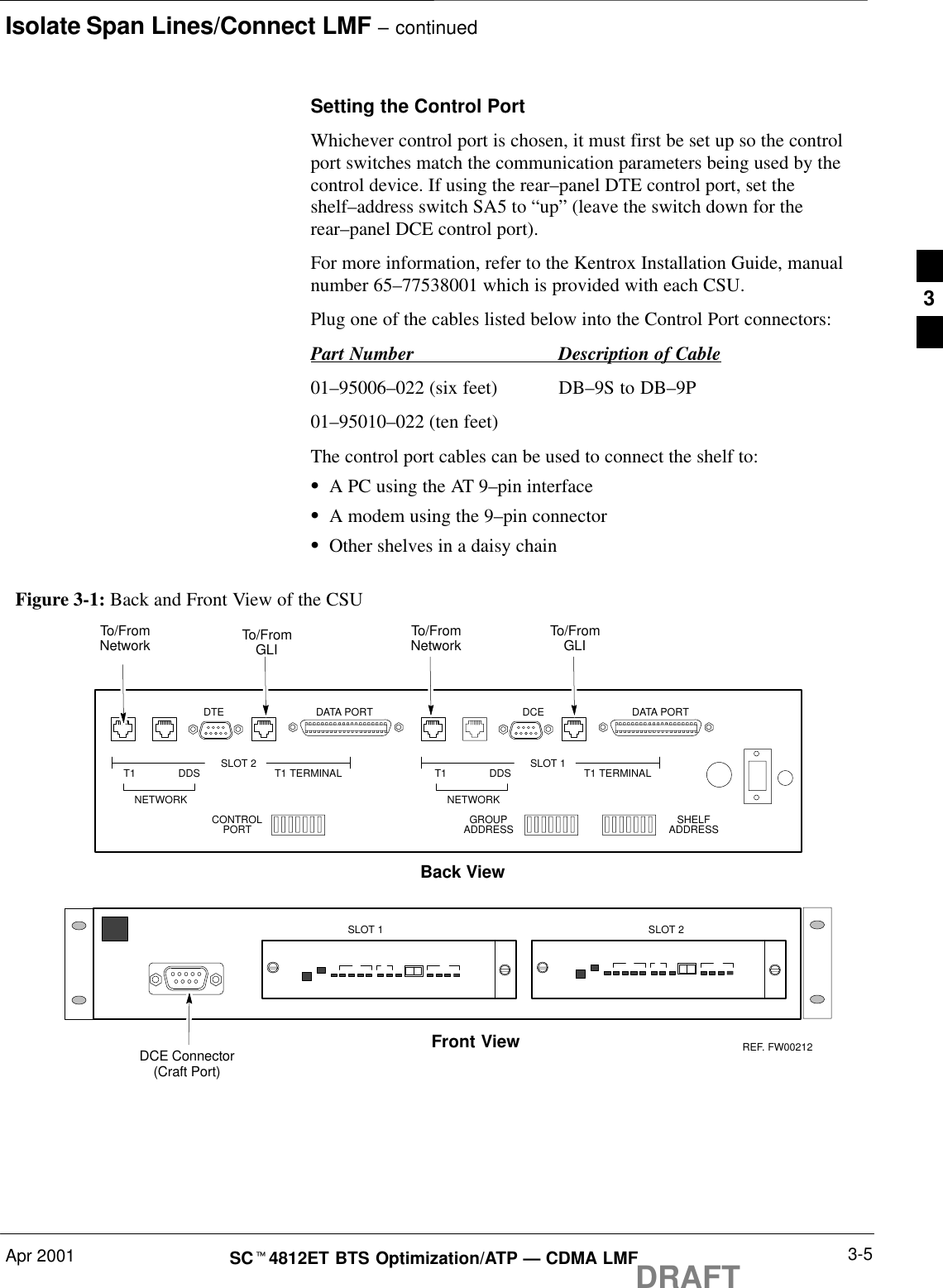
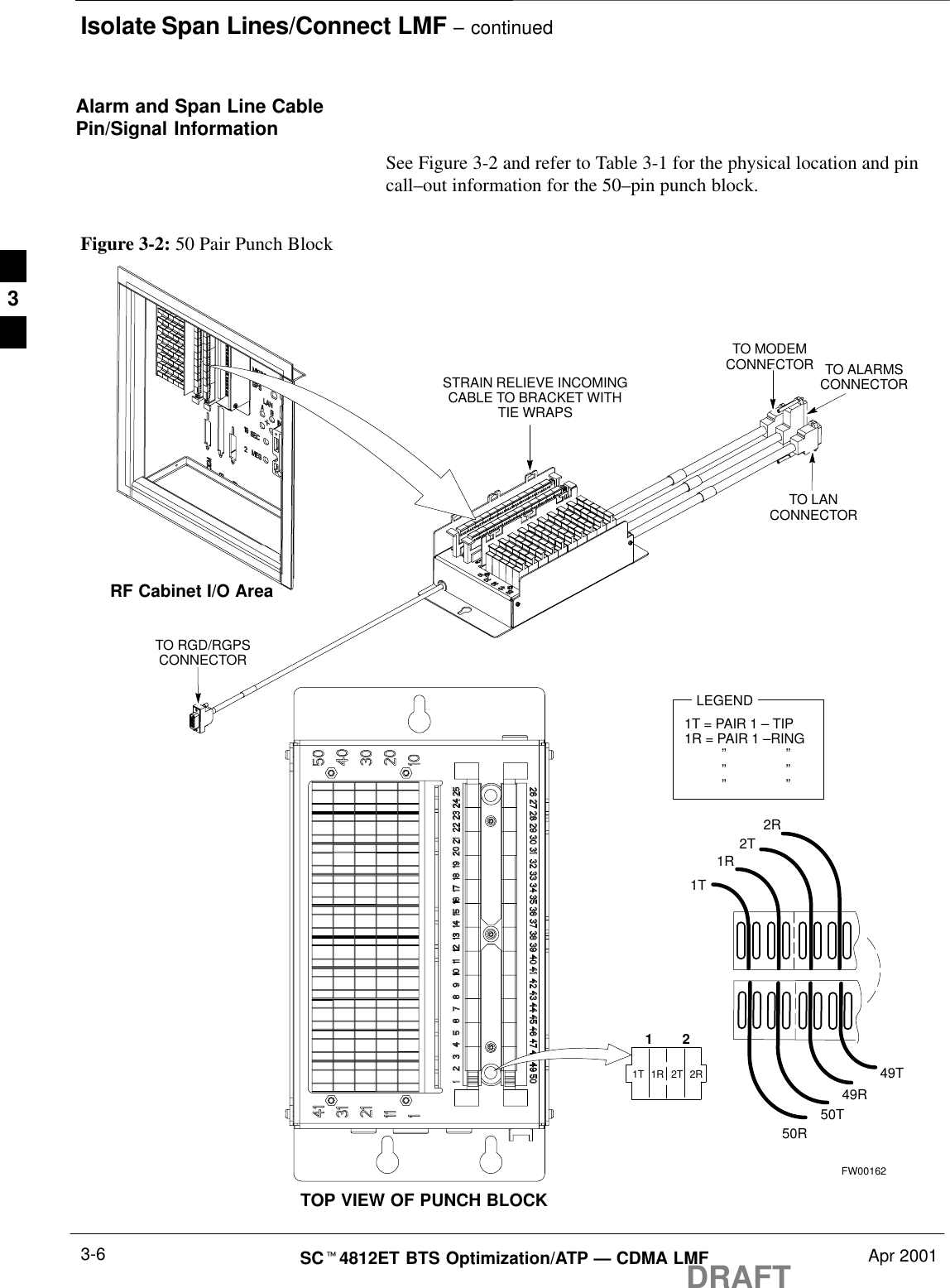
Isolate Span Lines/Connect LMF – continuedDRAFTSCt4812ET BTS Optimization/ATP — CDMA LMF Apr 20013-6Alarm and Span Line CablePin/Signal InformationSee Figure 3-2 and refer to Table 3-1 for the physical location and pincall–out information for the 50–pin punch block.Figure 3-2: 50 Pair Punch Block TOP VIEW OF PUNCH BLOCKSTRAIN RELIEVE INCOMINGCABLE TO BRACKET WITHTIE WRAPS2T1T 1R 2T 2R121R2RLEGEND1T = PAIR 1 – TIP1R = PAIR 1 –RING          ”                ”          ”                ”          ”                ”RF Cabinet I/O Area50R50T49R49T1TFW00162TO LANCONNECTORTO ALARMSCONNECTORTO MODEMCONNECTORTO RGD/RGPSCONNECTOR3
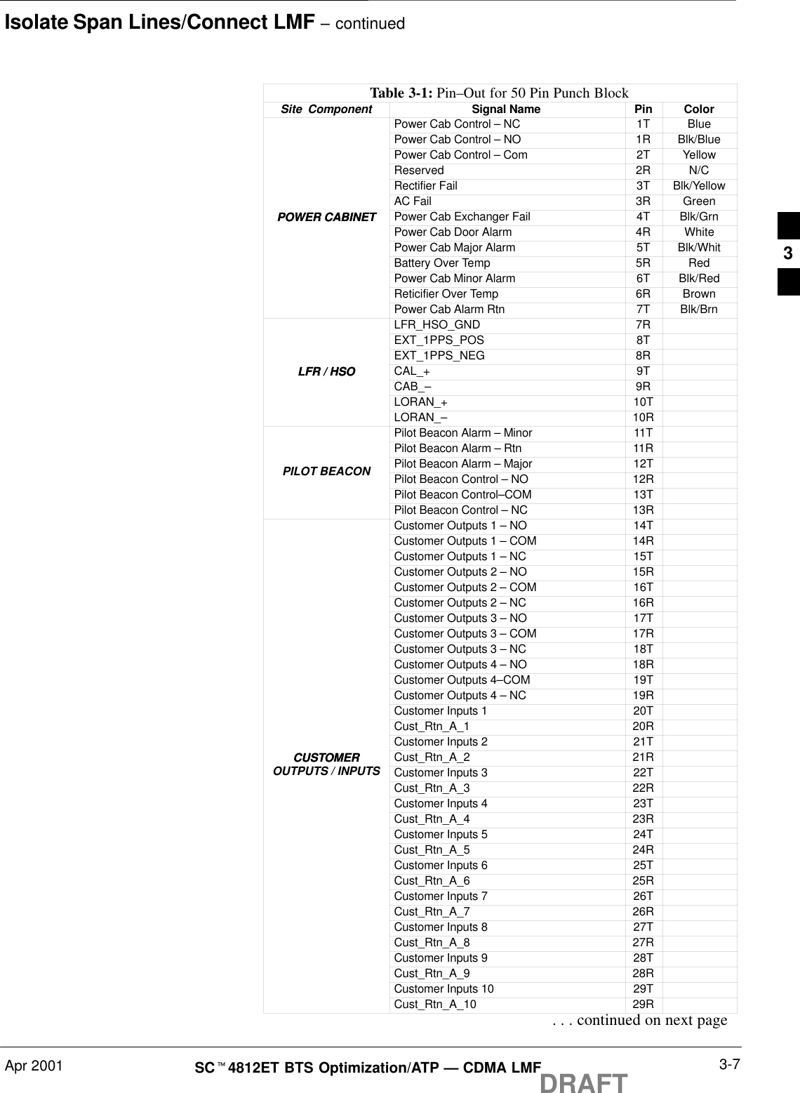
Isolate Span Lines/Connect LMF – continuedApr 2001 3-7SCt4812ET BTS Optimization/ATP — CDMA LMFDRAFTTable 3-1: Pin–Out for 50 Pin Punch BlockSite  Component Signal Name Pin ColorPower Cab Control – NC 1T BluePower Cab Control – NO 1R Blk/BluePower Cab Control – Com 2T YellowReserved 2R N/CRectifier Fail 3T Blk/YellowAC Fail 3R GreenPOWER CABINET Power Cab Exchanger Fail 4T Blk/GrnPOWER CABINET Power Cab Door Alarm 4R WhitePower Cab Major Alarm 5T Blk/WhitBattery Over Temp 5R RedPower Cab Minor Alarm 6T Blk/RedReticifier Over Temp 6R BrownPower Cab Alarm Rtn 7T Blk/BrnLFR_HSO_GND 7REXT_1PPS_POS 8TEXT_1PPS_NEG 8RLFR / HSO CAL_+ 9TLFR / HSO CAB_– 9RLORAN_+ 10TLORAN_– 10RPilot Beacon Alarm – Minor 11TPilot Beacon Alarm – Rtn 11RPilot Beacon Alarm – Major 12TPILOT BEACON Pilot Beacon Control – NO 12RPilot Beacon Control–COM 13TPilot Beacon Control – NC 13RCustomer Outputs 1 – NO 14TCustomer Outputs 1 – COM 14RCustomer Outputs 1 – NC 15TCustomer Outputs 2 – NO 15RCustomer Outputs 2 – COM 16TCustomer Outputs 2 – NC 16RCustomer Outputs 3 – NO 17TCustomer Outputs 3 – COM 17RCustomer Outputs 3 – NC 18TCustomer Outputs 4 – NO 18RCustomer Outputs 4–COM 19TCustomer Outputs 4 – NC 19RCustomer Inputs 1 20TCust_Rtn_A_1 20RCustomer Inputs 2 21TCUSTOMER Cust_Rtn_A_2 21RCUSTOMEROUTPUTS / INPUTS Customer Inputs 3 22TCust_Rtn_A_3 22RCustomer Inputs 4 23TCust_Rtn_A_4 23RCustomer Inputs 5 24TCust_Rtn_A_5 24RCustomer Inputs 6 25TCust_Rtn_A_6 25RCustomer Inputs 7 26TCust_Rtn_A_7 26RCustomer Inputs 8 27TCust_Rtn_A_8 27RCustomer Inputs 9 28TCust_Rtn_A_9 28RCustomer Inputs 10 29TCust_Rtn_A_10 29R. . . continued on next page3
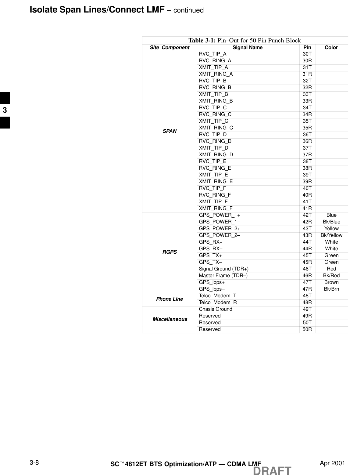
Isolate Span Lines/Connect LMF – continuedDRAFTSCt4812ET BTS Optimization/ATP — CDMA LMF Apr 20013-8Table 3-1: Pin–Out for 50 Pin Punch BlockSite  Component ColorPinSignal NameRVC_TIP_A 30TRVC_RING_A 30RXMIT_TIP_A 31TXMIT_RING_A 31RRVC_TIP_B 32TRVC_RING_B 32RXMIT_TIP_B 33TXMIT_RING_B 33RRVC_TIP_C 34TRVC_RING_C 34RXMIT_TIP_C 35TXMIT_RING_C 35RSPAN RVC_TIP_D 36TRVC_RING_D 36RXMIT_TIP_D 37TXMIT_RING_D 37RRVC_TIP_E 38TRVC_RING_E 38RXMIT_TIP_E 39TXMIT_RING_E 39RRVC_TIP_F 40TRVC_RING_F 40RXMIT_TIP_F 41TXMIT_RING_F 41RGPS_POWER_1+ 42T BlueGPS_POWER_1– 42R Bk/BlueGPS_POWER_2+ 43T YellowGPS_POWER_2– 43R Bk/YellowGPS_RX+ 44T WhiteGPS_RX– 44R WhiteRGPS GPS_TX+ 45T GreenGPS_TX– 45R GreenSignal Ground (TDR+) 46T RedMaster Frame (TDR–) 46R Bk/RedGPS_lpps+ 47T BrownGPS_lpps– 47R Bk/BrnTelco_Modem_T 48TPhone Line Telco_Modem_R 48RChasis Ground 49TReserved 49RMiscellaneous Reserved 50TReserved 50R  3
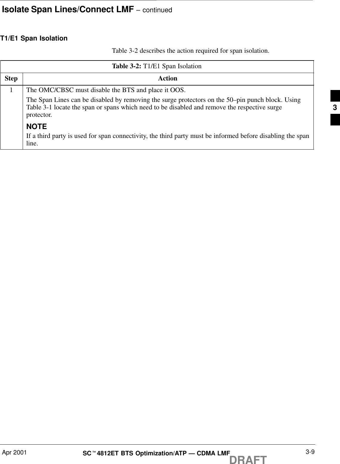
Isolate Span Lines/Connect LMF – continuedApr 2001 3-9SCt4812ET BTS Optimization/ATP — CDMA LMFDRAFTT1/E1 Span IsolationTable 3-2 describes the action required for span isolation.Table 3-2: T1/E1 Span IsolationStep Action1The OMC/CBSC must disable the BTS and place it OOS.The Span Lines can be disabled by removing the surge protectors on the 50–pin punch block. UsingTable 3-1 locate the span or spans which need to be disabled and remove the respective surgeprotector.NOTEIf a third party is used for span connectivity, the third party must be informed before disabling the spanline.3
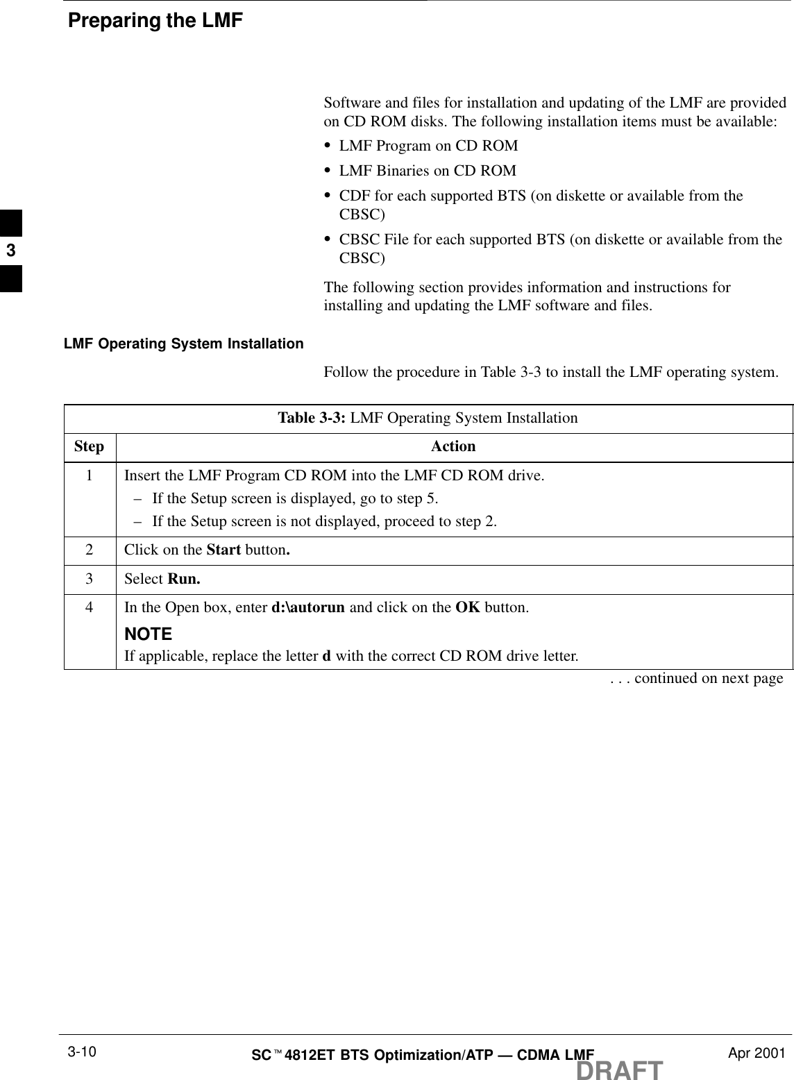
Preparing the LMFDRAFTSCt4812ET BTS Optimization/ATP — CDMA LMF Apr 20013-10Software and files for installation and updating of the LMF are providedon CD ROM disks. The following installation items must be available:SLMF Program on CD ROMSLMF Binaries on CD ROMSCDF for each supported BTS (on diskette or available from theCBSC)SCBSC File for each supported BTS (on diskette or available from theCBSC)The following section provides information and instructions forinstalling and updating the LMF software and files.LMF Operating System InstallationFollow the procedure in Table 3-3 to install the LMF operating system.Table 3-3: LMF Operating System InstallationStep Action1Insert the LMF Program CD ROM into the LMF CD ROM drive.–If the Setup screen is displayed, go to step 5.–If the Setup screen is not displayed, proceed to step 2.2Click on the Start button.3 Select Run.4In the Open box, enter d:\autorun and click on the OK button.NOTEIf applicable, replace the letter d with the correct CD ROM drive letter.. . . continued on next page3
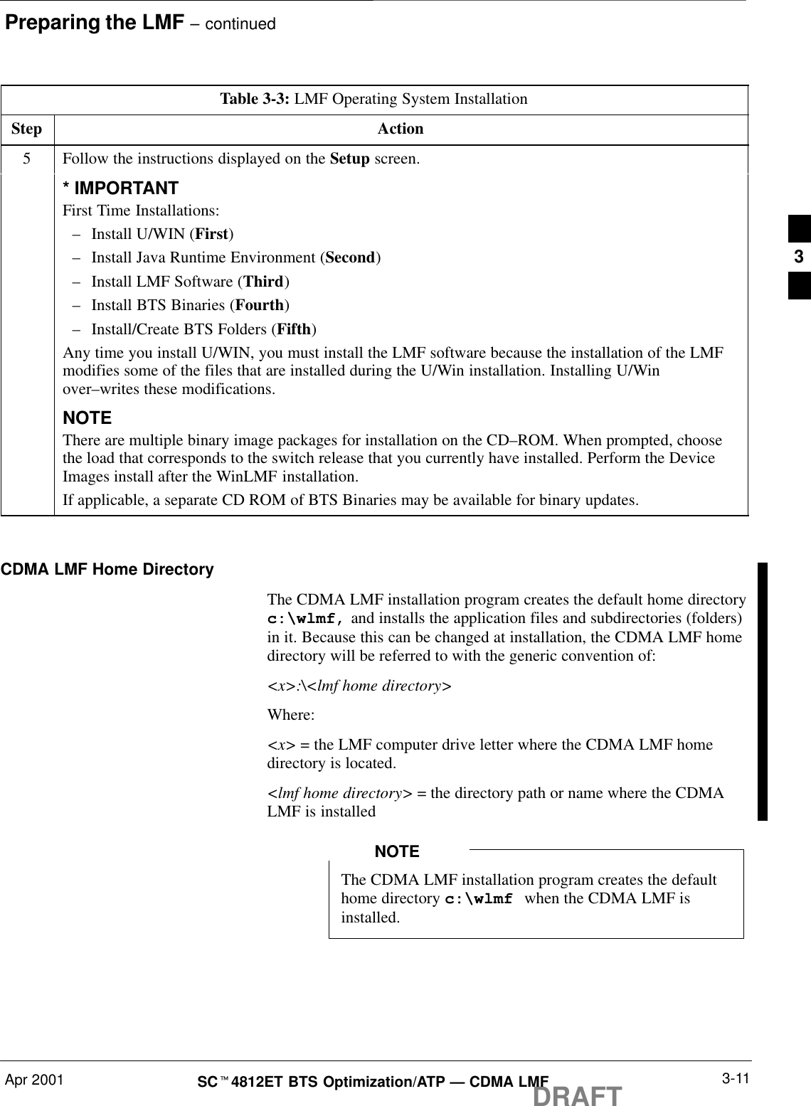
Preparing the LMF – continuedDRAFTApr 2001 3-11SCt4812ET BTS Optimization/ATP — CDMA LMFTable 3-3: LMF Operating System InstallationStep Action5Follow the instructions displayed on the Setup screen.* IMPORTANTFirst Time Installations:–Install U/WIN (First)–Install Java Runtime Environment (Second)–Install LMF Software (Third)–Install BTS Binaries (Fourth)–Install/Create BTS Folders (Fifth)Any time you install U/WIN, you must install the LMF software because the installation of the LMFmodifies some of the files that are installed during the U/Win installation. Installing U/Winover–writes these modifications.NOTEThere are multiple binary image packages for installation on the CD–ROM. When prompted, choosethe load that corresponds to the switch release that you currently have installed. Perform the DeviceImages install after the WinLMF installation.If applicable, a separate CD ROM of BTS Binaries may be available for binary updates. CDMA LMF Home DirectoryThe CDMA LMF installation program creates the default home directoryc:\wlmf, and installs the application files and subdirectories (folders)in it. Because this can be changed at installation, the CDMA LMF homedirectory will be referred to with the generic convention of:<x>:\<lmf home directory>Where:<x> = the LMF computer drive letter where the CDMA LMF homedirectory is located.<lmf home directory> = the directory path or name where the CDMALMF is installedThe CDMA LMF installation program creates the defaulthome directory c:\wlmf when the CDMA LMF isinstalled.NOTE3
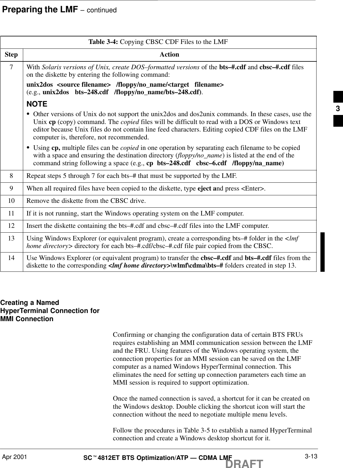
Preparing the LMF  – continuedDRAFTSCt4812ET BTS Optimization/ATP — CDMA LMF Apr 20013-12Copy CBSC CDF Files to theLMF ComputerBefore logging on to a BTS with the LMF to execute optimization/ATPprocedures, the correct bts-#.cdf and cbsc–#.cdf files must be obtainedfrom the CBSC and put in a bts-#  folder in the LMF computer. Thisrequires creating versions of the CBSC CDF files on a DOS–formattedfloppy diskette and using the diskette to install the CDF files on theLMF computer.*When copying CDF files, comply with the following toprevent BTS login problems with the LMF.– The numbers used in the bts–#.cdf and cbsc–#.cdffilenames must correspond to the locally assigned numbersfor each BTS and its controlling CBSC.– The generic cbsc–1.cdf file supplied with the LMF willwork with locally numbered BTS CDF files. Using this filewill not provide a valid optimization unless the generic fileis edited to replace default parameters (e.g., channelnumbers) with the operational parameters used locally.IMPORTANTThe procedure in Table 3-4 lists the steps required to transfer the CDFfiles from the CBSC to the LMF computer. For any further information,refer to the CDMA LMF Operator’s Guide (Motorola part number68P64114A21) or the LMF Help screen..Table 3-4: Copying CBSC CDF Files to the LMFStep Action1Login to the CBSC workstation.2Insert a DOS–formatted floppy diskette in the workstation drive.3 Type eject –q and press <Enter>.4 Type mount and press <Enter>.NOTESLook for the “floppy/no_name” message on the last line displayed.SIf the eject command was previously entered, floppy/no_name will be appended with a number. Usethe explicit floppy/no_name reference displayed when performing step 7.5Change to the directory, where the files to be copied reside, by typing cd <directoryname> (e.g., cd bts–248) and pressing <Enter>.6 Type ls and press the Enter key to display the list of files in the directory.. . . continued on next page3
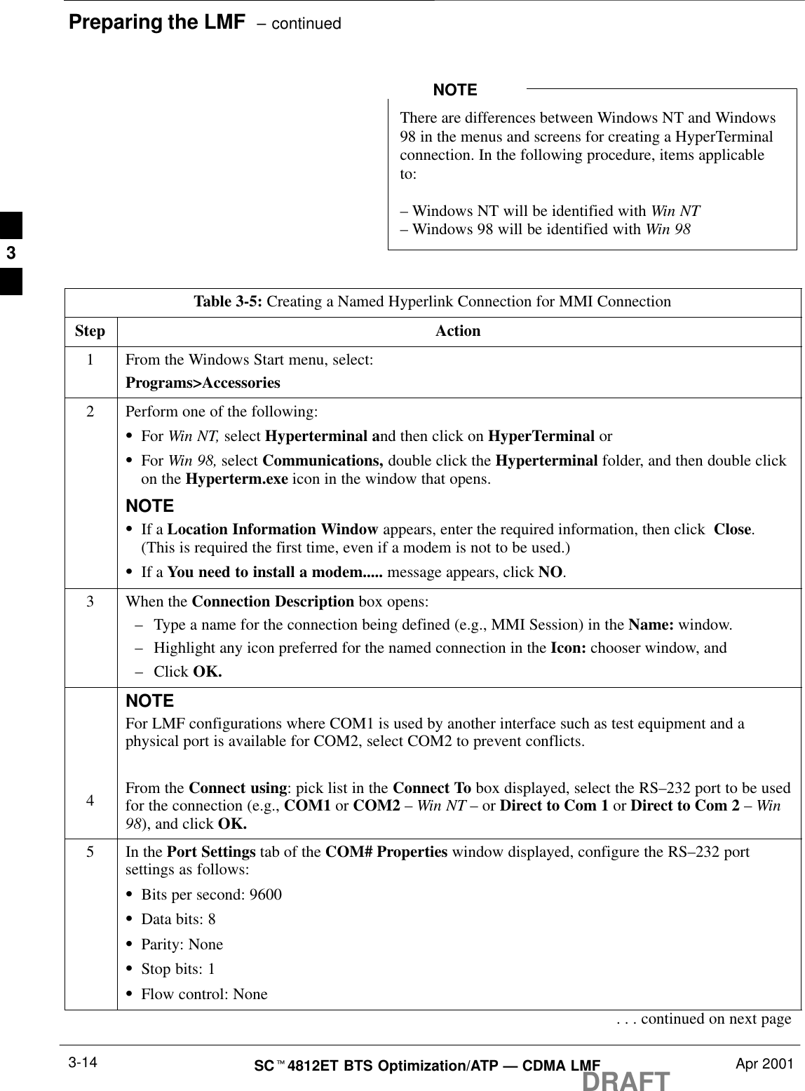
Preparing the LMF – continuedDRAFTApr 2001 3-13SCt4812ET BTS Optimization/ATP — CDMA LMFTable 3-4: Copying CBSC CDF Files to the LMFStep Action7 With Solaris versions of Unix, create DOS–formatted versions of the bts–#.cdf and cbsc–#.cdf fileson the diskette by entering the following command:unix2dos  <source filename>   /floppy/no_name/<target   filename>(e.g., unix2dos   bts–248.cdf   /floppy/no_name/bts–248.cdf).NOTESOther versions of Unix do not support the unix2dos and dos2unix commands. In these cases, use theUnix cp (copy) command. The copied files will be difficult to read with a DOS or Windows texteditor because Unix files do not contain line feed characters. Editing copied CDF files on the LMFcomputer is, therefore, not recommended.SUsing cp, multiple files can be copied in one operation by separating each filename to be copiedwith a space and ensuring the destination directory (floppy/no_name) is listed at the end of thecommand string following a space (e.g., cp  bts–248.cdf   cbsc–6.cdf   /floppy/na_name)8Repeat steps 5 through 7 for each bts–# that must be supported by the LMF.9When all required files have been copied to the diskette, type eject and press <Enter>.10 Remove the diskette from the CBSC drive.11 If it is not running, start the Windows operating system on the LMF computer.12 Insert the diskette containing the bts–#.cdf and cbsc–#.cdf files into the LMF computer.13 Using Windows Explorer (or equivalent program), create a corresponding bts–# folder in the <lmfhome directory> directory for each bts–#.cdf/cbsc–#.cdf file pair copied from the CBSC.14 Use Windows Explorer (or equivalent program) to transfer the cbsc–#.cdf and bts–#.cdf files from thediskette to the corresponding <lmf home directory>\wlmf\cdma\bts–# folders created in step 13. Creating a NamedHyperTerminal Connection forMMI ConnectionConfirming or changing the configuration data of certain BTS FRUsrequires establishing an MMI communication session between the LMFand the FRU. Using features of the Windows operating system, theconnection properties for an MMI session can be saved on the LMFcomputer as a named Windows HyperTerminal connection. Thiseliminates the need for setting up connection parameters each time anMMI session is required to support optimization.Once the named connection is saved, a shortcut for it can be created onthe Windows desktop. Double clicking the shortcut icon will start theconnection without the need to negotiate multiple menu levels.Follow the procedures in Table 3-5 to establish a named HyperTerminalconnection and create a Windows desktop shortcut for it.3
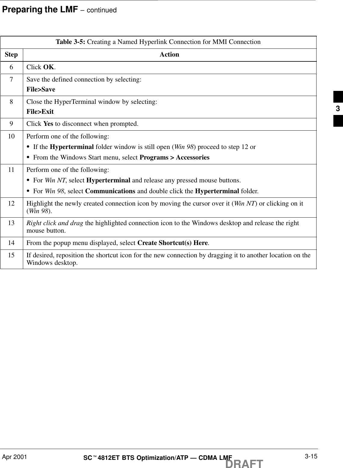
Preparing the LMF  – continuedDRAFTSCt4812ET BTS Optimization/ATP — CDMA LMF Apr 20013-14There are differences between Windows NT and Windows98 in the menus and screens for creating a HyperTerminalconnection. In the following procedure, items applicableto:– Windows NT will be identified with Win NT– Windows 98 will be identified with Win 98NOTETable 3-5: Creating a Named Hyperlink Connection for MMI ConnectionStep Action1From the Windows Start menu, select:Programs>Accessories2Perform one of the following:SFor Win NT, select Hyperterminal and then click on HyperTerminal orSFor Win 98, select Communications, double click the Hyperterminal folder, and then double clickon the Hyperterm.exe icon in the window that opens.NOTESIf a Location Information Window appears, enter the required information, then click  Close.(This is required the first time, even if a modem is not to be used.)SIf a You need to install a modem..... message appears, click NO.3When the Connection Description box opens:–Type a name for the connection being defined (e.g., MMI Session) in the Name: window.–Highlight any icon preferred for the named connection in the Icon: chooser window, and– Click OK.4NOTEFor LMF configurations where COM1 is used by another interface such as test equipment and aphysical port is available for COM2, select COM2 to prevent conflicts.From the Connect using: pick list in the Connect To box displayed, select the RS–232 port to be usedfor the connection (e.g., COM1 or COM2 – Win NT – or Direct to Com 1 or Direct to Com 2 – Win98), and click OK.5In the Port Settings tab of the COM# Properties window displayed, configure the RS–232 portsettings as follows:SBits per second: 9600SData bits: 8SParity: NoneSStop bits: 1SFlow control: None. . . continued on next page3
Preparing the LMF – continuedDRAFTApr 2001 3-15SCt4812ET BTS Optimization/ATP — CDMA LMFTable 3-5: Creating a Named Hyperlink Connection for MMI ConnectionStep Action6 Click OK.7Save the defined connection by selecting:File>Save8Close the HyperTerminal window by selecting:File>Exit9 Click Yes to disconnect when prompted.10 Perform one of the following:SIf the Hyperterminal folder window is still open (Win 98) proceed to step 12 orSFrom the Windows Start menu, select Programs > Accessories11 Perform one of the following:SFor Win NT, select Hyperterminal and release any pressed mouse buttons.SFor Win 98, select Communications and double click the Hyperterminal folder.12 Highlight the newly created connection icon by moving the cursor over it (Win NT) or clicking on it(Win 98).13 Right click and drag the highlighted connection icon to the Windows desktop and release the rightmouse button.14 From the popup menu displayed, select Create Shortcut(s) Here.15 If desired, reposition the shortcut icon for the new connection by dragging it to another location on theWindows desktop. 3
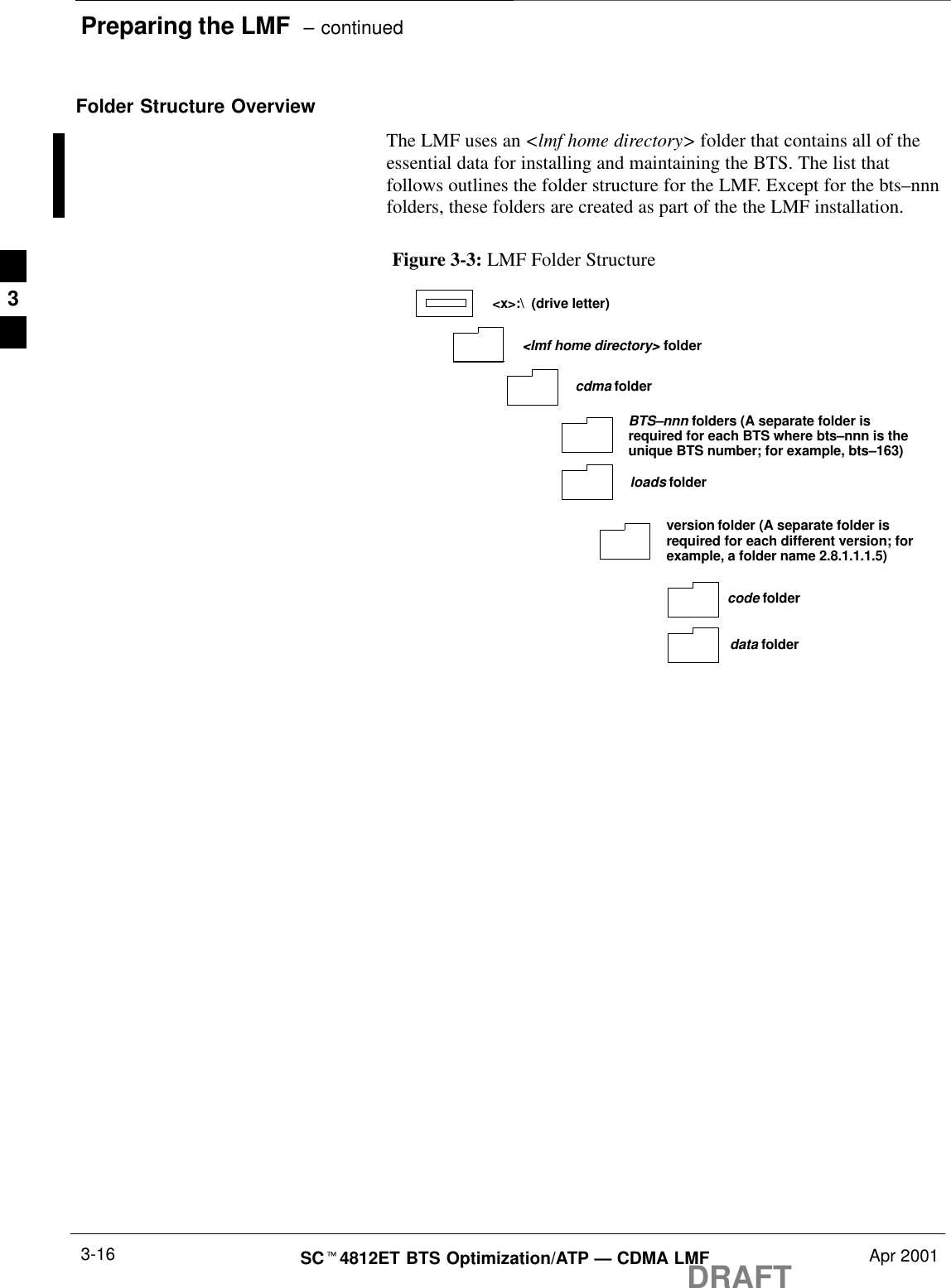
Preparing the LMF  – continuedDRAFTSCt4812ET BTS Optimization/ATP — CDMA LMF Apr 20013-16Folder Structure OverviewThe LMF uses an <lmf home directory> folder that contains all of theessential data for installing and maintaining the BTS. The list thatfollows outlines the folder structure for the LMF. Except for the bts–nnnfolders, these folders are created as part of the the LMF installation.Figure 3-3: LMF Folder Structureversion folder (A separate folder isrequired for each different version; forexample, a folder name 2.8.1.1.1.5)loads folder<x>:\  (drive letter)<lmf home directory> foldercdma foldercode folderdata folderBTS–nnn folders (A separate folder isrequired for each BTS where bts–nnn is theunique BTS number; for example, bts–163)3
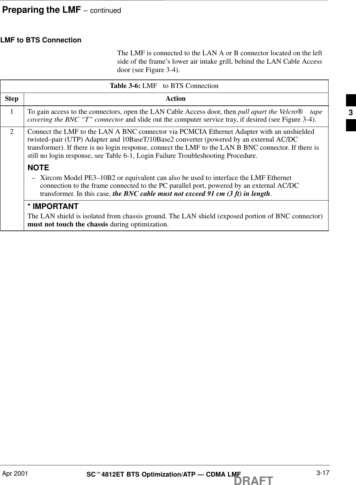
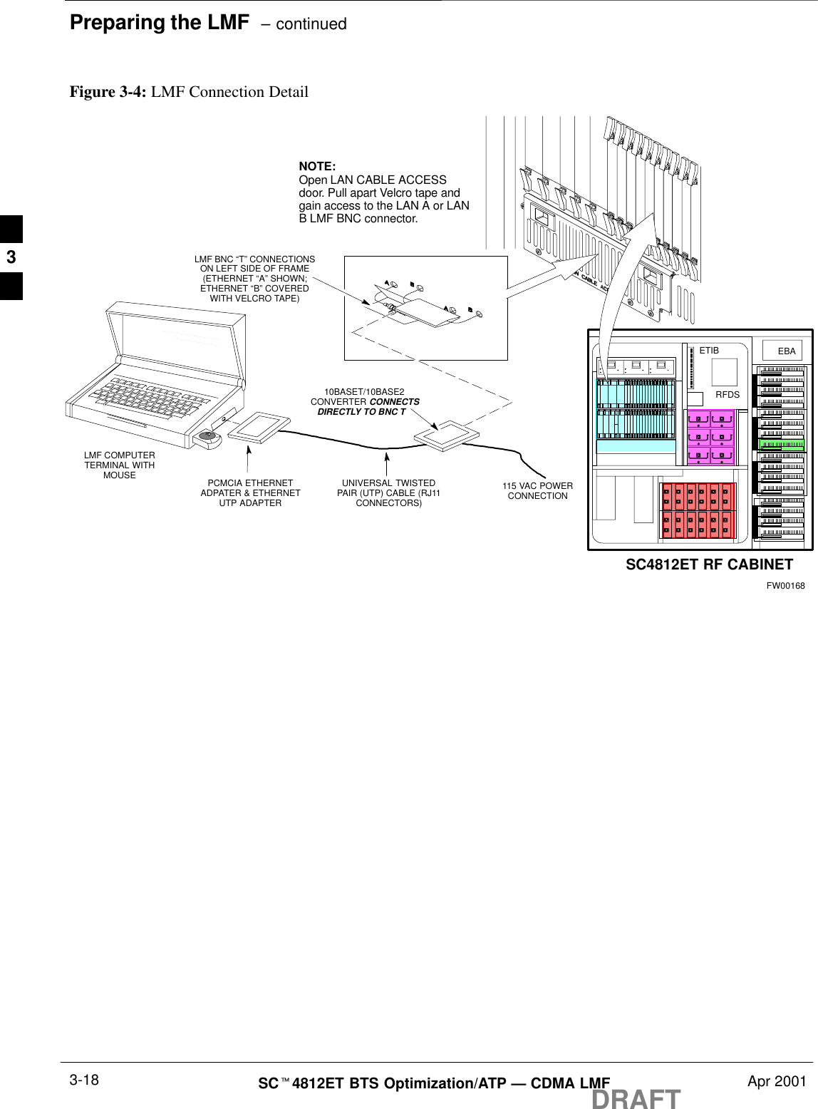
Preparing the LMF – continuedDRAFTApr 2001 3-17SCt4812ET BTS Optimization/ATP — CDMA LMFLMF to BTS ConnectionThe LMF is connected to the LAN A or B connector located on the leftside of the frame’s lower air intake grill, behind the LAN Cable Accessdoor (see Figure 3-4).Table 3-6: LMF   to BTS ConnectionStep Action1To gain access to the connectors, open the LAN Cable Access door, then pull apart the Velcro tapecovering the BNC “T” connector and slide out the computer service tray, if desired (see Figure 3-4).2Connect the LMF to the LAN A BNC connector via PCMCIA Ethernet Adapter with an unshieldedtwisted–pair (UTP) Adapter and 10BaseT/10Base2 converter (powered by an external AC/DCtransformer). If there is no login response, connect the LMF to the LAN B BNC connector. If there isstill no login response, see Table 6-1, Login Failure Troubleshooting Procedure.NOTE–Xircom Model PE3–10B2 or equivalent can also be used to interface the LMF Ethernetconnection to the frame connected to the PC parallel port, powered by an external AC/DCtransformer. In this case, the BNC cable must not exceed 91 cm (3 ft) in length.* IMPORTANTThe LAN shield is isolated from chassis ground. The LAN shield (exposed portion of BNC connector)must not touch the chassis during optimization.3
Preparing the LMF  – continuedDRAFTSCt4812ET BTS Optimization/ATP — CDMA LMF Apr 20013-18RFDSEBAETIBLMF BNC “T” CONNECTIONSON LEFT SIDE OF FRAME(ETHERNET “A” SHOWN;ETHERNET “B” COVEREDWITH VELCRO TAPE)LMF COMPUTERTERMINAL WITHMOUSE PCMCIA ETHERNETADPATER & ETHERNETUTP ADAPTERUNIVERSAL TWISTEDPAIR (UTP) CABLE (RJ11CONNECTORS)10BASET/10BASE2CONVERTER CONNECTSDIRECTLY TO BNC T   115 VAC POWERCONNECTIONFW00168SC4812ET RF CABINETNOTE:Open LAN CABLE ACCESSdoor. Pull apart Velcro tape andgain access to the LAN A or LANB LMF BNC connector.Figure 3-4: LMF Connection Detail3
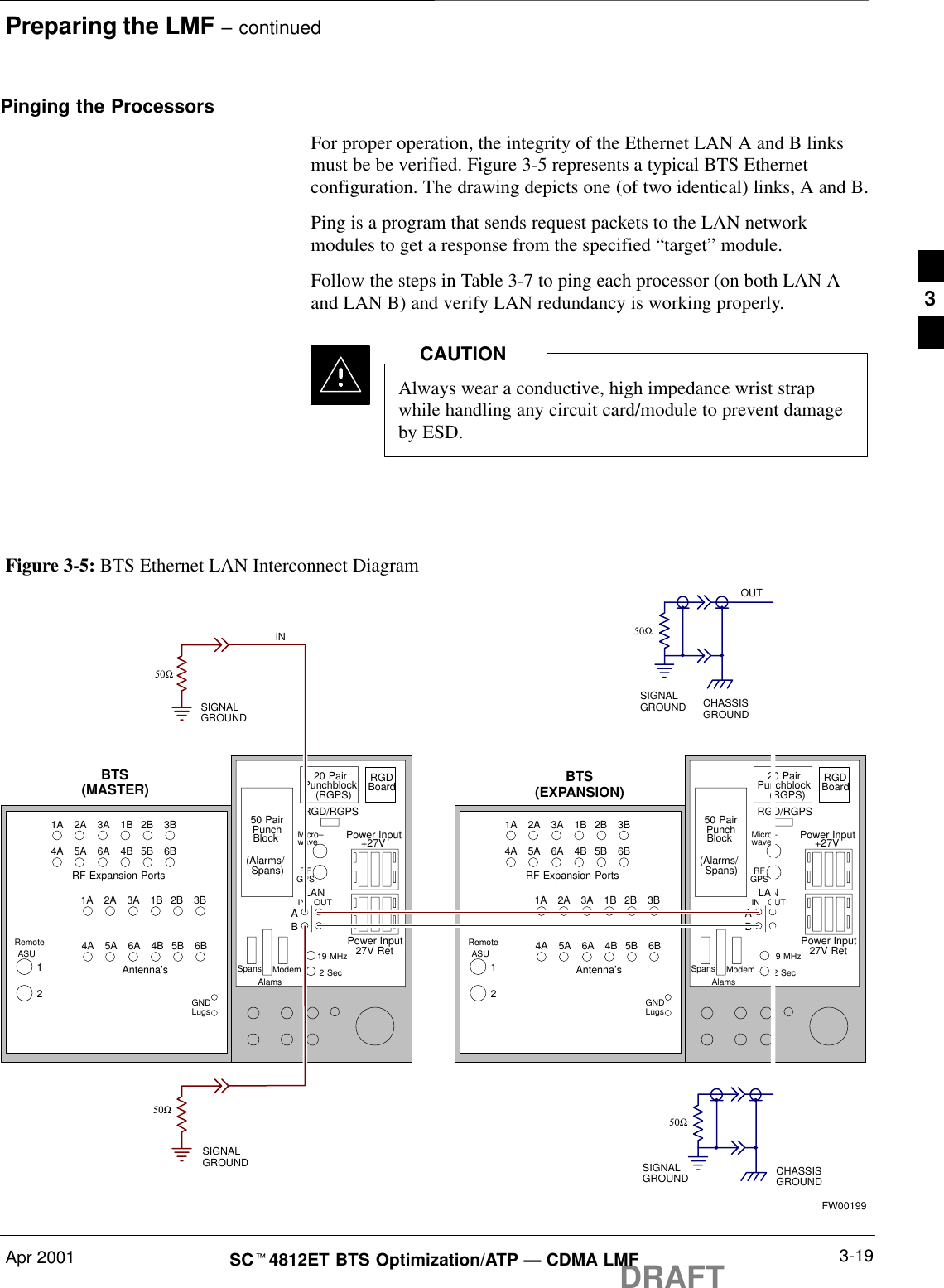
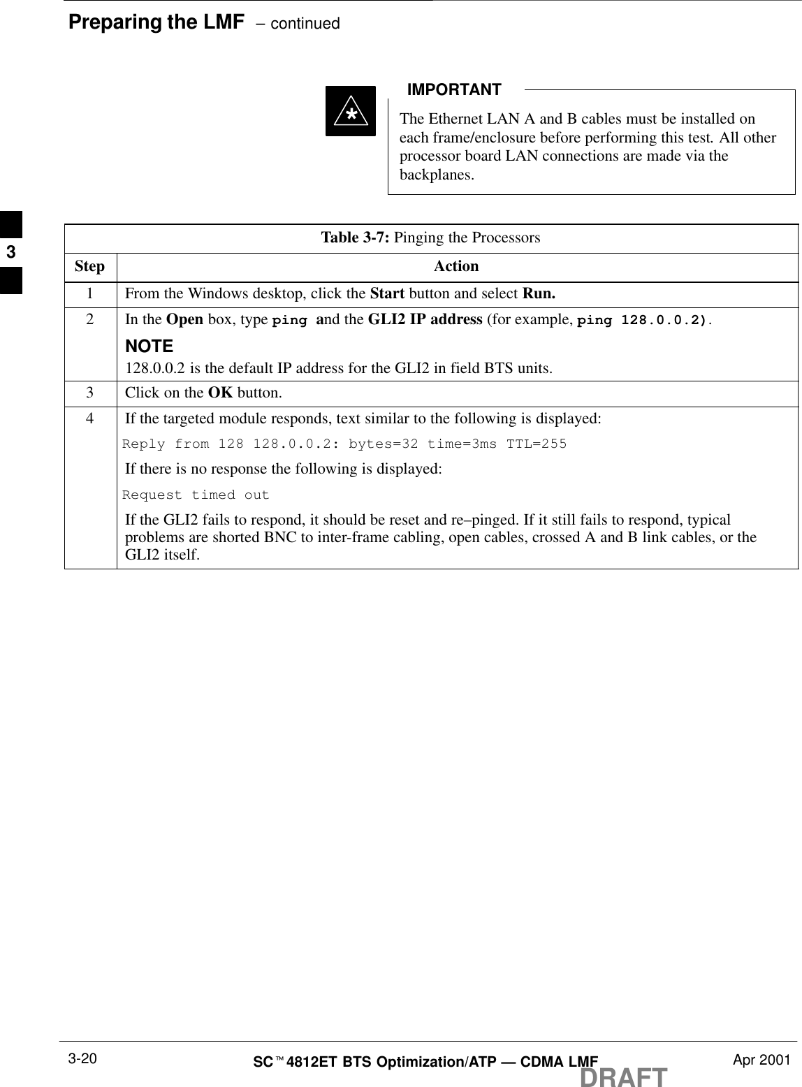
Preparing the LMF – continuedDRAFTApr 2001 3-19SCt4812ET BTS Optimization/ATP — CDMA LMFPinging the ProcessorsFor proper operation, the integrity of the Ethernet LAN A and B linksmust be be verified. Figure 3-5 represents a typical BTS Ethernetconfiguration. The drawing depicts one (of two identical) links, A and B.Ping is a program that sends request packets to the LAN networkmodules to get a response from the specified “target” module.Follow the steps in Table 3-7 to ping each processor (on both LAN Aand LAN B) and verify LAN redundancy is working properly.Always wear a conductive, high impedance wrist strapwhile handling any circuit card/module to prevent damageby ESD.CAUTIONRF Expansion PortsPunchBlock Power Input27V RetAntenna’s1A 2A 3A 1B 2B 3B4A 5A 6A 4B 5B 6B1A 2A 3A 1B 2B 3B4A 5A 6A 4B 5B 6B12RemoteASUGNDLugs50 Pair(Alarms/Punchblock20 Pair(RGPS)RGDBoardRGD/RGPSPower Input+27VMicro–waveRFGPSABIN OUTLAN19 MHz2 SecSpansAlamsModemSpans)RF Expansion PortsPunchBlock Power Input27V RetAntenna’s1A 2A 3A 1B 2B 3B4A 5A 6A 4B 5B 6B1A 2A 3A 1B 2B 3B4A 5A 6A 4B 5B 6B12RemoteASUGNDLugs50 Pair(Alarms/Punchblock20 Pair(RGPS)RGDBoardRGD/RGPSPower Input+27VMicro–waveRFGPSABIN OUTLAN19 MHz2 SecSpansAlamsModemSpans)CHASSISGROUNDSIGNALGROUND50ΩSIGNALGROUND50ΩINBTS(MASTER)OUTBTS(EXPANSION)CHASSISGROUNDSIGNALGROUND50ΩSIGNALGROUND50ΩFW00199Figure 3-5: BTS Ethernet LAN Interconnect Diagram3
Preparing the LMF  – continuedDRAFTSCt4812ET BTS Optimization/ATP — CDMA LMF Apr 20013-20*The Ethernet LAN A and B cables must be installed oneach frame/enclosure before performing this test. All otherprocessor board LAN connections are made via thebackplanes.IMPORTANTTable 3-7: Pinging the ProcessorsStep Action1From the Windows desktop, click the Start button and select Run.2In the Open box, type ping and the GLI2 IP address (for example, ping 128.0.0.2).NOTE128.0.0.2 is the default IP address for the GLI2 in field BTS units.3Click on the OK button.4If the targeted module responds, text similar to the following is displayed:Reply from 128 128.0.0.2: bytes=32 time=3ms TTL=255If there is no response the following is displayed:Request timed outIf the GLI2 fails to respond, it should be reset and re–pinged. If it still fails to respond, typicalproblems are shorted BNC to inter-frame cabling, open cables, crossed A and B link cables, or theGLI2 itself. 3
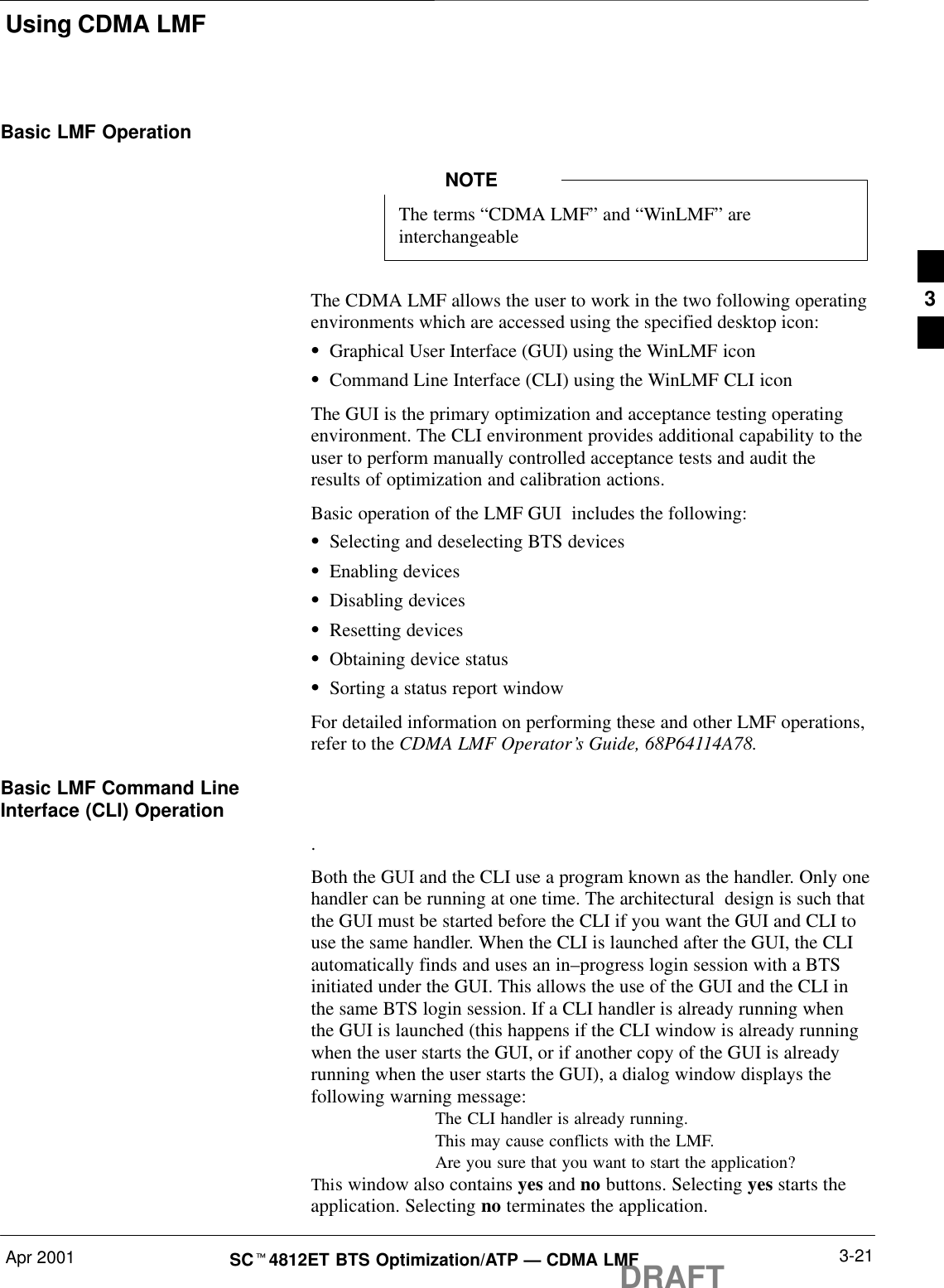
Using CDMA LMFDRAFTApr 2001 3-21SCt4812ET BTS Optimization/ATP — CDMA LMFBasic LMF OperationThe terms “CDMA LMF” and “WinLMF” areinterchangeableNOTEThe CDMA LMF allows the user to work in the two following operatingenvironments which are accessed using the specified desktop icon:SGraphical User Interface (GUI) using the WinLMF iconSCommand Line Interface (CLI) using the WinLMF CLI iconThe GUI is the primary optimization and acceptance testing operatingenvironment. The CLI environment provides additional capability to theuser to perform manually controlled acceptance tests and audit theresults of optimization and calibration actions.Basic operation of the LMF GUI  includes the following:SSelecting and deselecting BTS devicesSEnabling devicesSDisabling devicesSResetting devicesSObtaining device statusSSorting a status report windowFor detailed information on performing these and other LMF operations,refer to the CDMA LMF Operator’s Guide, 68P64114A78.Basic LMF Command LineInterface (CLI) Operation.Both the GUI and the CLI use a program known as the handler. Only onehandler can be running at one time. The architectural  design is such thatthe GUI must be started before the CLI if you want the GUI and CLI touse the same handler. When the CLI is launched after the GUI, the CLIautomatically finds and uses an in–progress login session with a BTSinitiated under the GUI. This allows the use of the GUI and the CLI inthe same BTS login session. If a CLI handler is already running whenthe GUI is launched (this happens if the CLI window is already runningwhen the user starts the GUI, or if another copy of the GUI is alreadyrunning when the user starts the GUI), a dialog window displays thefollowing warning message:The CLI handler is already running.This may cause conflicts with the LMF.Are you sure that you want to start the application?This window also contains yes and no buttons. Selecting yes starts theapplication. Selecting no terminates the application.3
Using CDMA LMF  – continuedDRAFTSCt4812ET BTS Optimization/ATP — CDMA LMF Apr 20013-22CLI Format ConventionsThe CLI command can be broken down in the following way:SverbSdevice including device identifier parametersSswitchSoption parameters consisting of:– keywords–equals sign (=) between the keyword and the parameter value–parameter valuesSpaces are required between the verb, device, switch, and optionparameters. A hyphen is required between the device and its identifiers.Following is an example of a CLI command.measure bbx–<bts_id>–<bbx_id> rssi channel=6 sector=5Refer to the LMF CLI Commands, R 15.X (68P09251A59) for acomplete explanation of the CLI commands and their use.Logging into a BTSBe sure that the correct bts–#.cdf and cbsc–#.cdf file isused for the BTS. These should be the CDF files that areprovided for the BTS by the CBSC. Failure to use thecorrect CDF files can result in wrong results. Failure touse the correct CDF files to log into a live (trafficcarrying) site can shut down the site.IMPORTANT*Logging into a BTS establishes a communications link between the BTSand the CDMA LMF. You may be logged into one or more BTS’s at atime, but only one LMF may be logged into each BTS.Before attempting to log into the BTS, confirm the CDMA LMF isproperly connected to the BTS (see Figure 3-4). Follow the procedure inTable 3-8 to log into a BTS.PrerequisitesBefore attempting to login to a BTS, ensure the following have beencompleted:SThe LMF is correctly installed and prepared.SA bts-nnn folder with the correct CDF and CBSC file exists.SThe LMF is correctly installed and prepared, and the LMF computerwas connected to the BTS before starting the Windows operatingsystem and LMF software. If necessary, restart the computer afterconnecting it to the BTS (see Table 3-6 and Figure 3-4).3
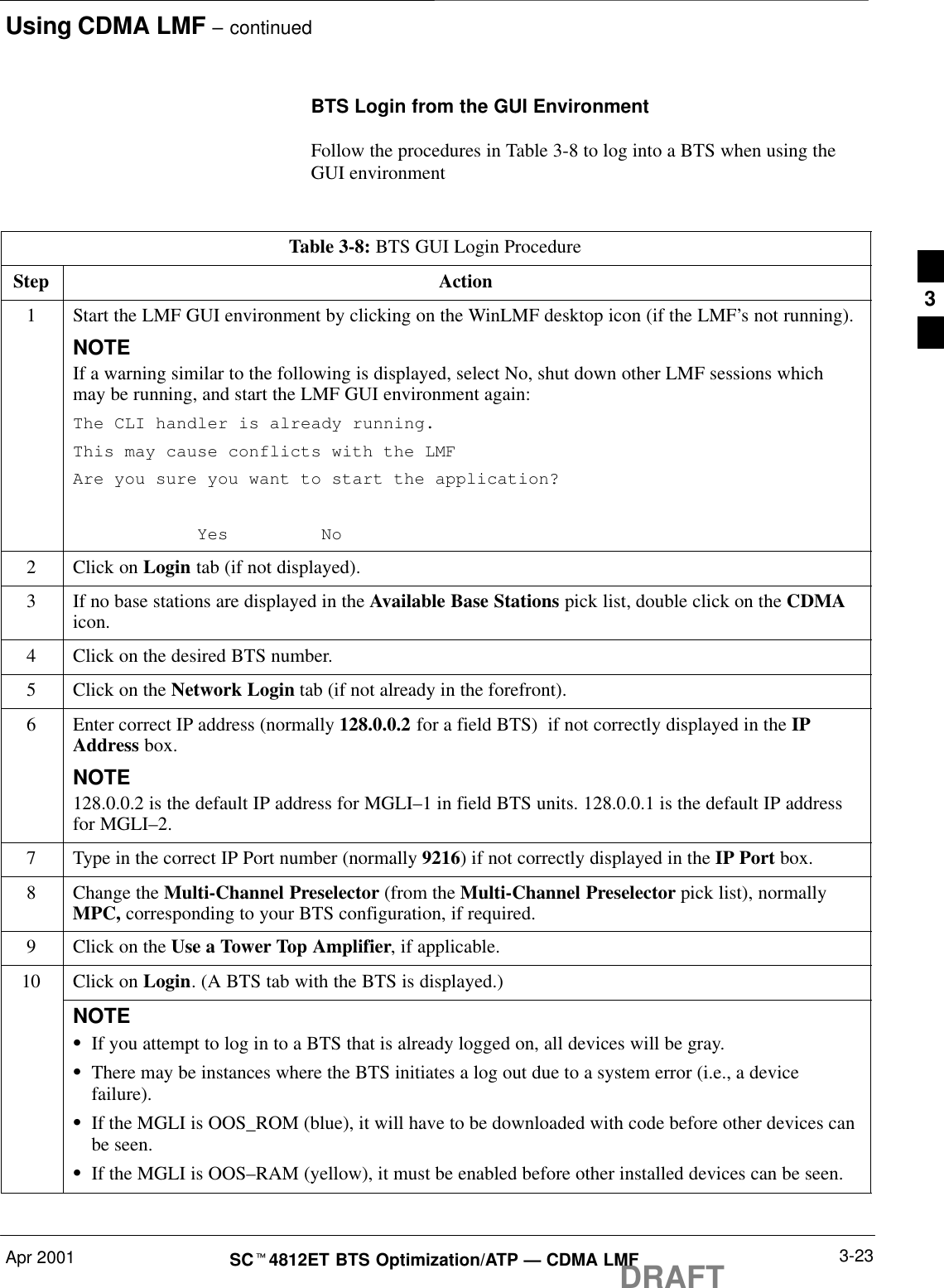
Using CDMA LMF – continuedDRAFTApr 2001 3-23SCt4812ET BTS Optimization/ATP — CDMA LMFBTS Login from the GUI EnvironmentFollow the procedures in Table 3-8 to log into a BTS when using theGUI environmentTable 3-8: BTS GUI Login ProcedureStep Action1Start the LMF GUI environment by clicking on the WinLMF desktop icon (if the LMF’s not running).NOTEIf a warning similar to the following is displayed, select No, shut down other LMF sessions whichmay be running, and start the LMF GUI environment again:The CLI handler is already running.This may cause conflicts with the LMFAre you sure you want to start the application?Yes No2Click on Login tab (if not displayed).3If no base stations are displayed in the Available Base Stations pick list, double click on the CDMAicon.4Click on the desired BTS number.5Click on the Network Login tab (if not already in the forefront).6Enter correct IP address (normally 128.0.0.2 for a field BTS)  if not correctly displayed in the IPAddress box.NOTE128.0.0.2 is the default IP address for MGLI–1 in field BTS units. 128.0.0.1 is the default IP addressfor MGLI–2.7Type in the correct IP Port number (normally 9216) if not correctly displayed in the IP Port box.8Change the Multi-Channel Preselector (from the Multi-Channel Preselector pick list), normallyMPC, corresponding to your BTS configuration, if required.9Click on the Use a Tower Top Amplifier, if applicable.10 Click on Login. (A BTS tab with the BTS is displayed.)NOTESIf you attempt to log in to a BTS that is already logged on, all devices will be gray.SThere may be instances where the BTS initiates a log out due to a system error (i.e., a devicefailure).SIf the MGLI is OOS_ROM (blue), it will have to be downloaded with code before other devices canbe seen.SIf the MGLI is OOS–RAM (yellow), it must be enabled before other installed devices can be seen. 3
Using CDMA LMF  – continuedDRAFTSCt4812ET BTS Optimization/ATP — CDMA LMF Apr 20013-24BTS Login from the CLI EnvironmentFollow the procedures in Table 3-9 to log into a BTS when using theGUI environmentTable 3-9: BTS CLI Login ProcedureStep Action1Double click the WinLMF CLI desktop icon (if the LMF CLI environment is not already running).NOTEIf a BTS was logged into under a GUI session when the CLI environment was started, the CLI sessionwill be logged into the same BTS, and step 2 is not required.2At the /wlmf prompt, enter the following command:login bts–<bts#>   host=<host>   port=<port>where:host = MGLI card IP address (defaults to address last logged into for this BTS or 128.0.0.2 if this isfirst login to this BTS).port = IP port of the TS (defaults to port last logged into for this BTS or 9216 if this is first login tothis BTS)Logging OutLogging out of a BTS is accomplished differently for the GUI and theCLI operating environments.The GUI and CLI environments use the same connection toa BTS. If a BTS is logged into in both the GUI and the CLIenvironments at the same time, logging out of the BTS ineither environment will log out of it for both.  When eithera login or logout is performed in the CLI window, there isno GUI indication that the login or logout has occurred.IMPORTANT*Logging Out of a BTS from the GUI EnvironmentFollow the procedure in Table 3-10 to logout of a BTS when using theGUI environment.Table 3-10: BTS GUI Logout ProcedureStep Action1Click on Select on the BTS tab menu bar.2Click the Logout item in the pulldown menu (a Confirm Logout pop–up message will appear).. . . continued on next page3
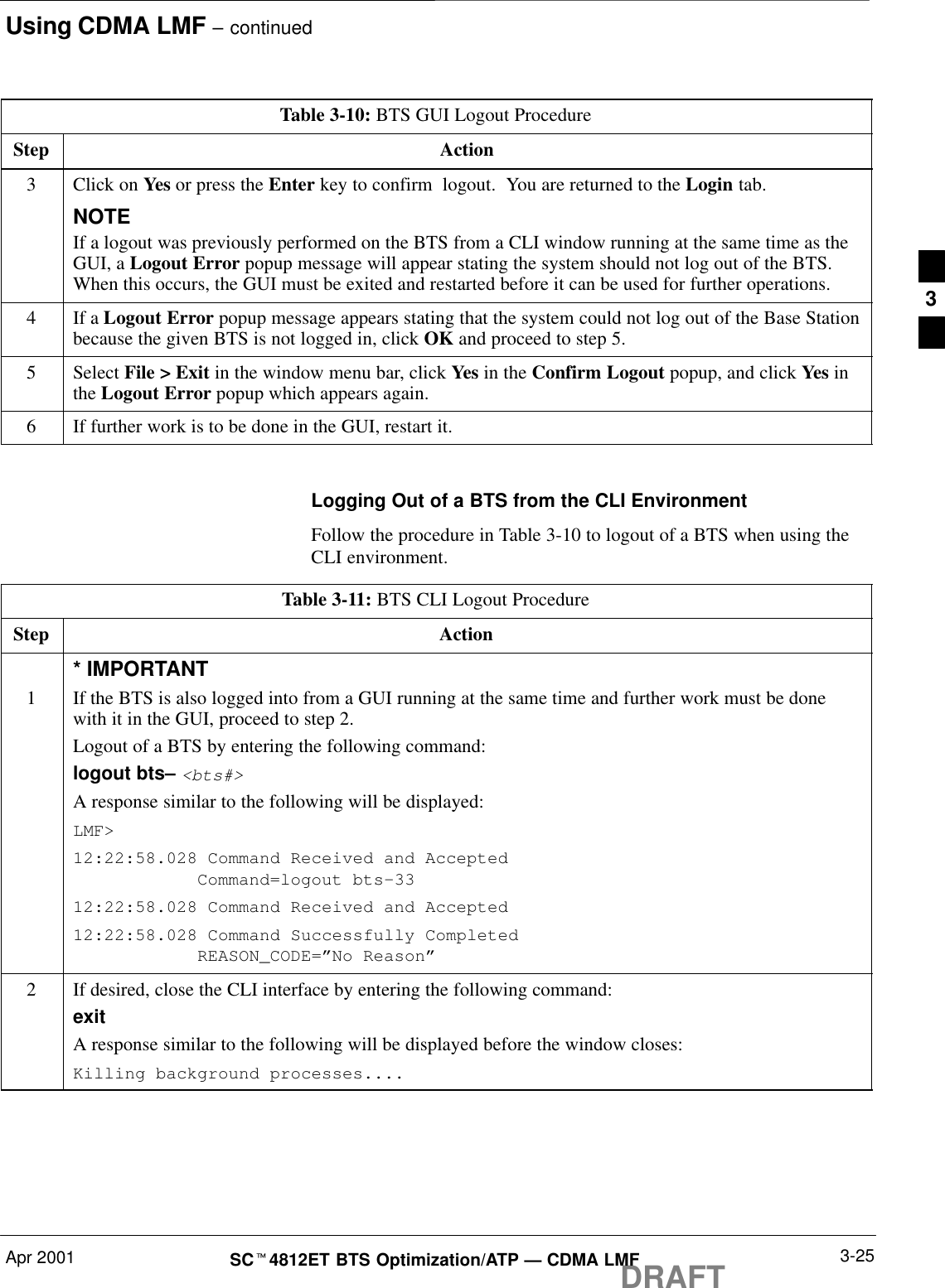
Using CDMA LMF – continuedDRAFTApr 2001 3-25SCt4812ET BTS Optimization/ATP — CDMA LMFTable 3-10: BTS GUI Logout ProcedureStep Action3Click on Yes or press the Enter key to confirm  logout.  You are returned to the Login tab.NOTEIf a logout was previously performed on the BTS from a CLI window running at the same time as theGUI, a Logout Error popup message will appear stating the system should not log out of the BTS.When this occurs, the GUI must be exited and restarted before it can be used for further operations.4If a Logout Error popup message appears stating that the system could not log out of the Base Stationbecause the given BTS is not logged in, click OK and proceed to step 5.5 Select File > Exit in the window menu bar, click Yes in the Confirm Logout popup, and click Yes inthe Logout Error popup which appears again.6If further work is to be done in the GUI, restart it. Logging Out of a BTS from the CLI EnvironmentFollow the procedure in Table 3-10 to logout of a BTS when using theCLI environment.Table 3-11: BTS CLI Logout ProcedureStep Action1* IMPORTANTIf the BTS is also logged into from a GUI running at the same time and further work must be donewith it in the GUI, proceed to step 2.Logout of a BTS by entering the following command:logout bts– <bts#>A response similar to the following will be displayed:LMF>12:22:58.028 Command Received and Accepted            Command=logout bts–3312:22:58.028 Command Received and Accepted12:22:58.028 Command Successfully Completed            REASON_CODE=”No Reason”2If desired, close the CLI interface by entering the following command:exitA response similar to the following will be displayed before the window closes:Killing background processes.... 3
Using CDMA LMF  – continuedDRAFTSCt4812ET BTS Optimization/ATP — CDMA LMF Apr 20013-26Establishing an MMICommunication SessionFor those procedures that require MMI communications between theLMF and BTS FRUs, follow the procedure in Table 3-12 to initiate thecommunication session.Table 3-12: Establishing MMI CommunicationsStep Action1Connect the LMF computer to the equipment as detailed in the applicable procedure that requiresMMI communication session.2Start the named HyperTerminal connection for MMI sessions by double clicking on its Windowsdesktop shortcut.NOTEIf a Windows desktop shortcut was not created for the MMI connection, access the connection fromthe Windows Start menu by selecting:Programs>Accessories>Hyperterminal>HyperTerminal><Named HyperTerminal Connection(e.g., MMI Session).3Once the connection window opens, establish MMI communication with the BTS FRU by pressingthe LMF computer Enter key until the prompt identified in the applicable procedure is obtained. NULL MODEMBOARD(TRN9666A)8–PIN TO 10–PINRS–232 CABLE (P/N30–09786R01)RS–232 CABLE8–PINCDMA LMFCOMPUTERTo FRU MMI portDB9–TO–DB25ADAPTERFigure 3-6: CDMA LMF Computer Common MMI ConnectionsCOM1ORCOM2FW006873
Download the BTSApr 2001 3-27SCt4812ET BTS Optimization/ATP — CDMA LMFDRAFTDownload CodeCode can be downloaded to a device that is in any state. After thedownload starts, the device being downloaded changes toOOS_ROM (blue). If the download is completed successfully, the devicechanges to OOS_RAM with code loaded (yellow). Prior to downloadinga device, a code file must exist. The code file is selected automatically ifthe code file is in the /lmf/cdma/n.n.n.n/code folder (where n.n.n.n is theversion number of the download code that matches the “NextLoad”parameter in the CDF file). The code file in the code folder must havethe correct hardware bin number. Code can be automatically or manuallyselected.The following are the devices to be downloaded:SSpan Configuration–Master Group Line Interface (MGLI2)–Slave Group Line Interface (SGLI2)SClock Synchronization Manager (CSM)SMulti Channel Card (MCC24E or MCC8E)SBroadband Transceiver (BBX2)STest Subscriber Interface Card (TSIC) – if RFDS is installedThe MGLI must be successfully downloaded with code anddata, and put INS before downloading any other device.The download code process for an MGLI automaticallydownloads data and enables the MGLI before downloadingother devices. The other devices can be downloaded in anyorder.IMPORTANT*Follow the procedure in Table 3-13 to download the firmwareapplication code for the MGLI2. The download code action downloadsdata and also enables the MGLI2.PrerequisitesPrior to performing these procedures, ensure a code file exists for each ofthe devices to be downloaded.3
Download the BTS – continuedDRAFTSCt4812ET BTS Optimization/ATP — CDMA LMF Apr 20013-28All devices in a BTS must have the same R–level ROMand RAM code before the optimization and ATPprocedures can be performed. If a newly installed BTS is tobe upgraded, the optimization and ATPs should beaccomplished with the prior code load. Then the siteshould be upgraded by the CBSC. The optimization andATP procedures do not have to be performed again afterthe upgrade. If a replacement device needs to be used in aBTS with a later version of software, the device ROM codecan be changed with use of the LMF before theoptimization and ATPs are performed for the BTS. Refer tothe Download ROM Code section.WARNINGTable 3-13: Download and Enable MGLI2Step Action1 Select Util>Tools>Update Next Load function to ensure the Next Load parameter is set to the correctcode version level.2Download code to the primary MGLI2 by clicking on the MGLI2.–From the Device pull down menu, select Download Code.A status report confirms change in the device(s) status.– Click OK to close the status window. (The MGLI2 should automatically be downloaded with dataand enabled.)3Download code and data to the redundant MGLI2 but do not enable at this time. Download Code and Data toNon–MGLI2 DevicesNon–MGLI2 devices can be downloaded individually or all equippeddevices can be downloaded with one action. Follow the procedure inTable 3-14 to download code and data to the non–MGLI2 devices.When downloading multiple devices, the download mayfail for some of the devices (a time out occurs). Thesedevices can be downloaded separately after completing themultiple download.NOTE3
Download the BTS – continuedApr 2001 3-29SCt4812ET BTS Optimization/ATP — CDMA LMFDRAFTTable 3-14: Download Code and Data to Non–MGLI DevicesStep Action1Select all devices to be downloaded.2From the Device pull down menu, select Download Code.A status report displays the result of the download for each selected device.Click OK to close the status window.NOTEAfter the download has started, the device being downloaded changes to blue. If the download iscompleted successfully, the device changes to yellow (OOS-RAM with code loaded).After a BBX, CSM or MCC is successfully downloaded with code and has changed to OOS-RAM, thestatus LED should be rapidly flashing GREEN.3To download the firmware application data to each device, select the target device and select:Device>Download Data Select CSM Clock SourceA CSM can have three different clock sources. The Select CSM Sourcefunction can be used to select the clock source for each of the threeinputs. This function is only used if the clock source for a CSM needs tobe changed. The Clock Source function provides the following clocksource options.SLocal GPSSRemote GPSSHSO (only for source 2 & 3)SLFR (only for source 2 & 3)S10 MHz (only for source 2 & 3)SNONE (only for source 2 & 3)PrerequisitesMGLI=INS_ACT, CSM= OOS_RAM or INS_ACTTable 3-15: Select CSM Clock SourceStep Action1Select the applicable CSM(s).2Click on the Device menu.3Click on the Clock Source menu item.4Click on the Select menu item. A clock source selection window is displayed.5Select the applicable clock source in the Clock Reference Source pick lists. Uncheck the relatedcheck box if you do not want the displayed pick list item to be used.6Click on the OK button. A status report window is displayed showing the results of the selectionaction.7Click on the OK button to close the status report window. 3
Download the BTS – continuedDRAFTSCt4812ET BTS Optimization/ATP — CDMA LMF Apr 20013-30Enable CSMsEach BTS CSM system features two CSM boards per site. In a typicaloperation, the primary CSM locks its Digital Phase Locked Loop(DPLL) circuits to GPS signals. These signals are generated by either anon–board GPS module (RF–GPS) or a remote GPS receiver (R–GPS).The CSM2 card is required when using the R–GPS. The GPS receiver(mounted on CSM 1) is used as the primary timing reference andsynchronizes the entire cellular system. CSM 2 provides redundancy (butdoes not have a GPS receiver).The BTS may be equipped with a LORAN–C LFR, HSO, or external 10MHz Rubidium source which the CSM can use as a secondary timingreference. In all cases, the CSM monitors and determines what referenceto use at a given time.For RF–GPS, verify the CSM configured with the GPSreceiver “daughter board” is installed in the frame’s CSM 1slot before continuing.IMPORTANT*Follow the steps outlined in Table 3-16 to enable the CSMs installed inthe C–CCP shelves.Table 3-16: Enable CSMsStep Action1Click on the target CSM.From the Device pull down, select Enable.NOTEIf equipped with two CSMs, enable CSM–2 firstA status report is displayed confirming change in the device(s) status.Click OK to close the status report window.NOTEFAIL may be shown in the status table for enable action. If Waiting For Phase Lock is shown in theDescription field, the CSM changes to the Enabled state after phase lock is achieved.CSM 1 houses the GPS receiver. The enable sequence can take up to one hour (see below).* IMPORTANTThe GPS satellite system satellites are not in a geosynchronous orbit and are maintained and operatedby the United States Department of Defense (D.O.D.). The D.O.D. periodically alters satellite orbits;therefore, satellite trajectories are subject to change. A GPS receiver that is INS contains an “almanac”that is updated periodically to take these changes into account.If a GPS receiver has not been updated for a number of weeks, it may take up to an hour for the GPSreceiver “almanac” to be updated.Once updated, the GPS receiver must track at least four satellites and obtain (hold) a 3–D position fixfor a minimum of 45 seconds before the CSM will come in service. (In some cases, the GPS receiverneeds to track only one satellite, depending on accuracy mode set during the data load).. . . continued on next page3
Download the BTS – continuedApr 2001 3-31SCt4812ET BTS Optimization/ATP — CDMA LMFDRAFTTable 3-16: Enable CSMsStep Action2NOTEIf equipped with two CSMs, CSM–1 should be bright green (INS–ACT) and CSM–2 should be darkgreen(INS–STB)If more than an hour has passed, refer to CSM Verification, see Figure 3-7 and Table 3-19 to determinethe cause.NOTEAfter the CSMs have been successfully enabled, observe the PWR/ALM LEDs are steady green(alternating green/red indicates the card is in an alarm state). Enable MCCsThis procedure configures the MCC and sets the “tx fine adjust”parameter. The “tx fine adjust” parameter is not a transmit gain setting,but a timing adjustment that compensates for the processing delay in theBTS (approximately 3 mS).Follow the steps outlined in Table 3-17 to enable the MCCs installed inthe C–CCP shelves.The MGLI and CSM must be downloaded and enabled,prior to downloading and enabling the MCC.IMPORTANT*Table 3-17: Enable MCCsStep Action1Click on the target MCC(s) or from the Select pull down menu choose All MCCs.2From the Device menu, select EnableA status report is displayed confirming change in the device(s) status.3 Click OK to close the status report window. 3
CSM System Time – GPS & LFR/HSO VerificationDRAFTSCt4812ET BTS Optimization/ATP — CDMA LMF Apr 20013-32Clock SynchronizationManager System TimeThe primary function of the Clock Synchronization Manager (CSM)boards (slots 1 and 2) is to maintain CDMA system time. The CSM inslot 1 is the primary timing source while slot 2 provides redundancy.The CSM2 card (CSM second generation) is required when using theremote GPS receiver (R–GPS). R–GPS uses a GPS receiver in theantenna head that has a digital output to the CSM2 card. CSM2 can havea daughter card as a local GPS receiver to support an RF–GPS signal.The CSM2 switches between the primary and redundant units (slots 1and 2) upon failure or command. CDMA Clock Distribution Cards(CCDs) buffer and distribute even–second reference and 19.6608 MHzclocks. CCD 1 is married to CSM 1 and CCD 2 is married to CSM 2. Afailure on CSM 1 or CCD 1 cause the system to switch to redundantCSM 2 and CCD 2.Each CSM2 board features an ovenized, crystal oscillator that provides19.6608 MHz clock, even second pulse, and 3 MHz referenced to theselected synchronization source (see Table 3-19):SGPS: local/RF–GPS or remote/R–GPSSLORAN–C Frequency Receiver (LFR) or High Stability Oscillator(HSO)SExternal reference oscillator sourcesFault management has the capability of switching between the GPSsynchronization source and the LFR/HSO backup source in the event ofa GPS receiver failure on CSM 1. During normal operation, the CSM 1board selects GPS as the primary source (see Table 3-19). The sourceselection can also be overridden via the LMF or by the system software.Synchronization between the primary and redundant CSM CCD pairs, aswell as the LFR or HSO back–up to GPS synchronization, increasesreliability.Low Frequency Receiver/High Stability OscillatorThe CSM handles the overall configuration and status monitoringfunctions of the LFR/HSO. In the event of GPS failure, the LFR/HSO iscapable of maintaining synchronization initially established by the GPSreference signal.The LFR requires an active external antenna to receive LORAN RFsignals.  Timing pulses are derived from this signal, which issynchronized to Universal Time Coordinates (UTC) and GPS time. TheLFR can maintain system time indefinately after initial GPS lock.3
CSM System Time – GPS & LFR/HSO Verification – continuedApr 2001 3-33SCt4812ET BTS Optimization/ATP — CDMA LMFDRAFTThe HSO is a high stability 10 MHz oscillator with the necessaryinterface to the CSMs.  The HSO is typically installed in thosegeographical areas not covered by the LORAN–C system. Since theHSO is a free–standing oscillator, system time can only be maintainedfor 24 hours after 24 hours of GPS lock.Upgrades and Expansions: LFR2/HSO2/HSOXLFR2/HSO2 (second generation cards) both export a timing signal to theexpansion or logical BTS frames. The associated expansion or logicalframes require an HSO–expansion (HSOX) whether the starter frame hasan LFR2 or an HSO2. The HSOX accepts input from the starter frameand interfaces with the CSM cards in the expansion frame. LFR andLFR2 use the same source code in source selection (see Table 3-19).HSO, HSO2, and HSOX use the same source code in source selection(see Table 3-19).Allow the base site and test equipment to warm up for60 minutes after any interruption in oscillator power.CSM board warm-up allows the oscillator oventemperature and oscillator frequency to stabilize prior totest.  Test equipment warm-up allows the Rubidiumstandard timebase to stabilize in frequency before anymeasurements are made.NOTE3
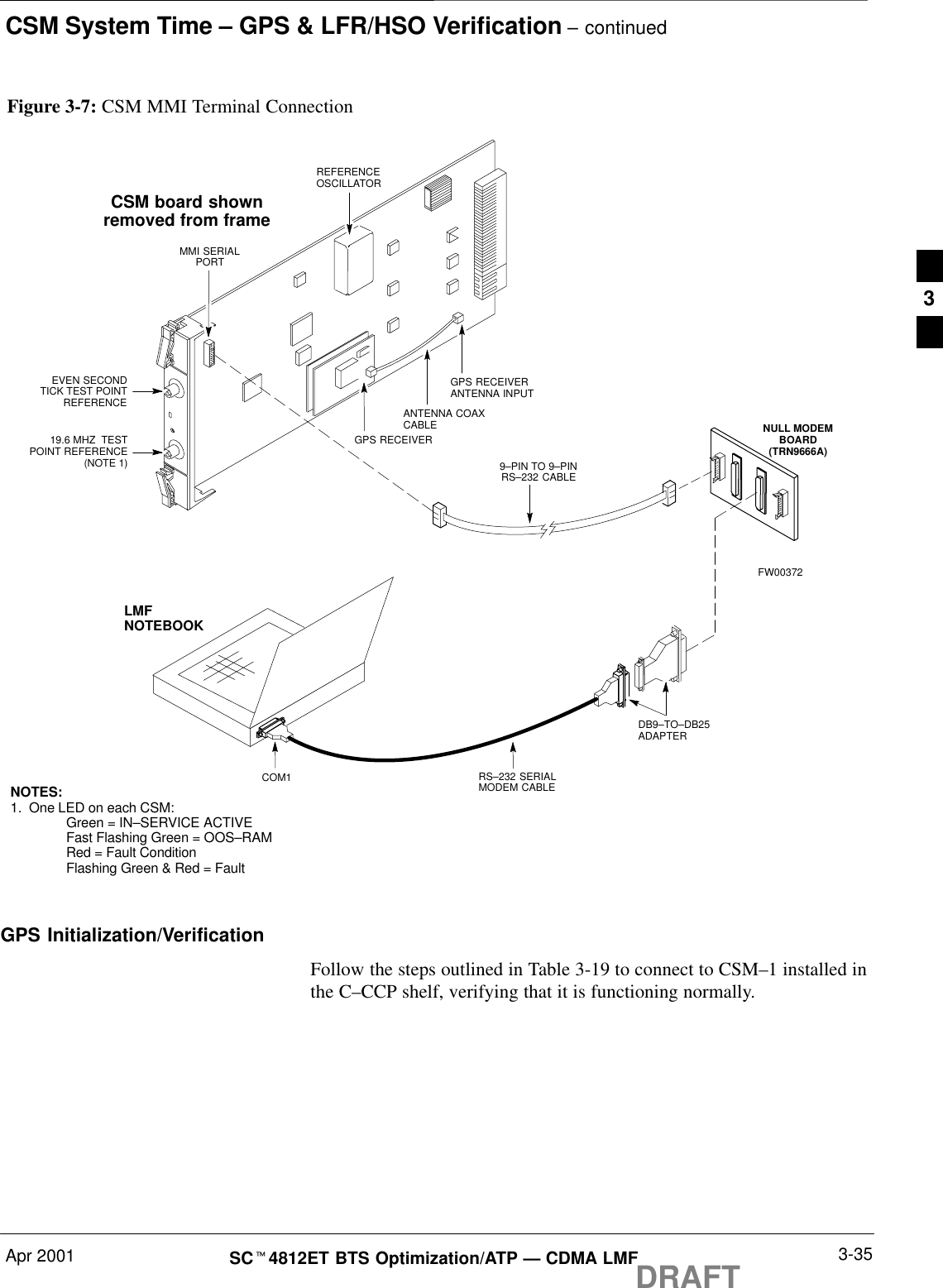
CSM System Time – GPS & LFR/HSO Verification – continuedDRAFTSCt4812ET BTS Optimization/ATP — CDMA LMF Apr 20013-34CSM Frequency VerificationThe objective of this procedure is the initial verification of the CSMboards before performing the rf path verification tests. Parts of thisprocedure will be repeated for final verification after the overalloptimization has been completed.Test Equipment Setup (GPS & LFR/HSO Verification)Follow the steps outlined in Table 3-18 to set up test equipment.Table 3-18: Test Equipment Setup (GPS & LFR/HSO Verification)Step Action1a For local GPS (RF–GPS): Verify a CSM board with a GPS receiver is installed in primary CSM slot 1and that CSM–1 is INS.NOTEThis is verified by checking the board ejectors for kit number SGLN1145 on the board in slot 1.1b For Remote GPS (RGPS):Verify a CSM2 board is installed in primary slot 1 and that CSM–1 is INS.NOTEThis is verified by checking the board ejectors for kit number SGLN4132CC (or subsequent).2Remove CSM–2 (if installed) and connect a serial cable from the LMF COM 1 port (via null modemboard) to the MMI port on CSM–1 (see Figure 3-7).3Reinstall CSM–2.4Start an MMI communication session with CSM–1 by using the Windows desktop shortcut icon (seeTable 3-5)NOTEThe LMF program must be running when a  Hyperterminal session is started.5When the terminal screen appears press the Enter key until the CSM> prompt appears.SConnect GPS antenna to the (GPS) RF connectorONLY. Damage to the GPS antenna and/or receivercan result if the GPS antenna is inadvertently connectedto any other RF connector.CAUTION3
CSM System Time – GPS & LFR/HSO Verification – continuedApr 2001 3-35SCt4812ET BTS Optimization/ATP — CDMA LMFDRAFTNULL MODEMBOARD(TRN9666A)RS–232 SERIALMODEM CABLEDB9–TO–DB25ADAPTERCOM1LMFNOTEBOOKFigure 3-7: CSM MMI Terminal ConnectionFW00372CSM board shownremoved from frame19.6 MHZ  TESTPOINT REFERENCE(NOTE 1)EVEN SECONDTICK TEST POINTREFERENCEGPS RECEIVERANTENNA INPUTGPS RECEIVERMMI SERIALPORTANTENNA COAXCABLEREFERENCEOSCILLATOR9–PIN TO 9–PINRS–232 CABLENOTES:1. One LED on each CSM:Green = IN–SERVICE ACTIVEFast Flashing Green = OOS–RAMRed = Fault ConditionFlashing Green & Red = FaultGPS Initialization/VerificationFollow the steps outlined in Table 3-19 to connect to CSM–1 installed inthe C–CCP shelf, verifying that it is functioning normally.3
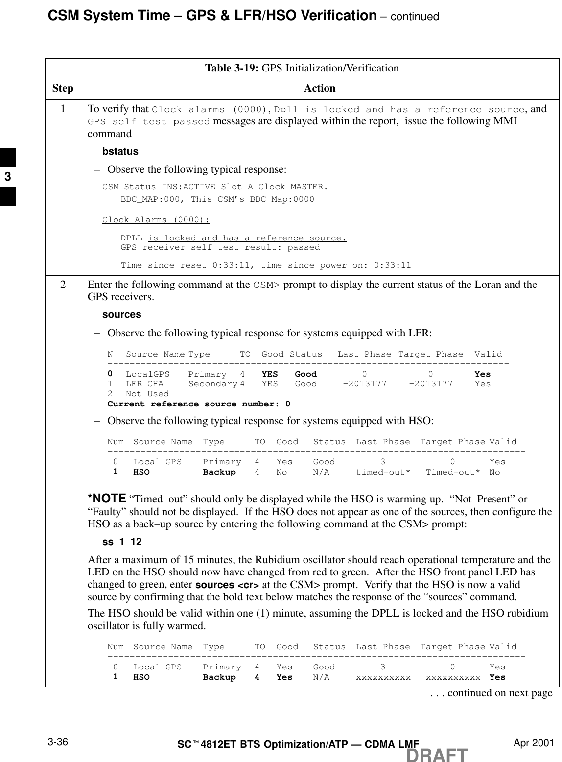
CSM System Time – GPS & LFR/HSO Verification – continuedDRAFTSCt4812ET BTS Optimization/ATP — CDMA LMF Apr 20013-36Table 3-19: GPS Initialization/VerificationStep Action1To verify that Clock alarms (0000), Dpll is locked and has a reference source, andGPS self test passed messages are displayed within the report,  issue the following MMIcommandbstatus–Observe the following typical response:CSM Status INS:ACTIVE Slot A Clock MASTER.BDC_MAP:000, This CSM’s BDC Map:0000Clock Alarms (0000):DPLL is locked and has a reference source.GPS receiver self test result: passedTime since reset 0:33:11, time since power on: 0:33:112Enter the following command at the CSM> prompt to display the current status of the Loran and theGPS receivers.sources–Observe the following typical response for systems equipped with LFR:N Source Name Type TO Good Status Last Phase Target Phase Valid–––––––––––––––––––––––––––––––––––––––––––––––––––––––––––––––––––––––––0LocalGPS Primary 4 YES Good 00Yes1 LFR CHA Secondary 4 YES Good –2013177 –2013177 Yes2 Not UsedCurrent reference source number: 0–Observe the following typical response for systems equipped with HSO:Num Source Name Type TO Good Status Last Phase Target Phase Valid––––––––––––––––––––––––––––––––––––––––––––––––––––––––––––––––––––––––––––0 Local GPS Primary 4 Yes Good 3 0 Yes1HSO Backup 4 No N/A timed–out* Timed–out* No*NOTE “Timed–out” should only be displayed while the HSO is warming up.  “Not–Present” or“Faulty” should not be displayed.  If the HSO does not appear as one of the sources, then configure theHSO as a back–up source by entering the following command at the CSM> prompt:ss 1 12After a maximum of 15 minutes, the Rubidium oscillator should reach operational temperature and theLED on the HSO should now have changed from red to green.  After the HSO front panel LED haschanged to green, enter sources <cr> at the CSM> prompt.  Verify that the HSO is now a validsource by confirming that the bold text below matches the response of the “sources” command.The HSO should be valid within one (1) minute, assuming the DPLL is locked and the HSO rubidiumoscillator is fully warmed.Num Source Name Type TO Good Status Last Phase Target Phase Valid––––––––––––––––––––––––––––––––––––––––––––––––––––––––––––––––––––––––––––0 Local GPS Primary 4 Yes Good 3 0 Yes1HSO Backup 4 Yes N/A xxxxxxxxxx xxxxxxxxxx Yes. . . continued on next page3
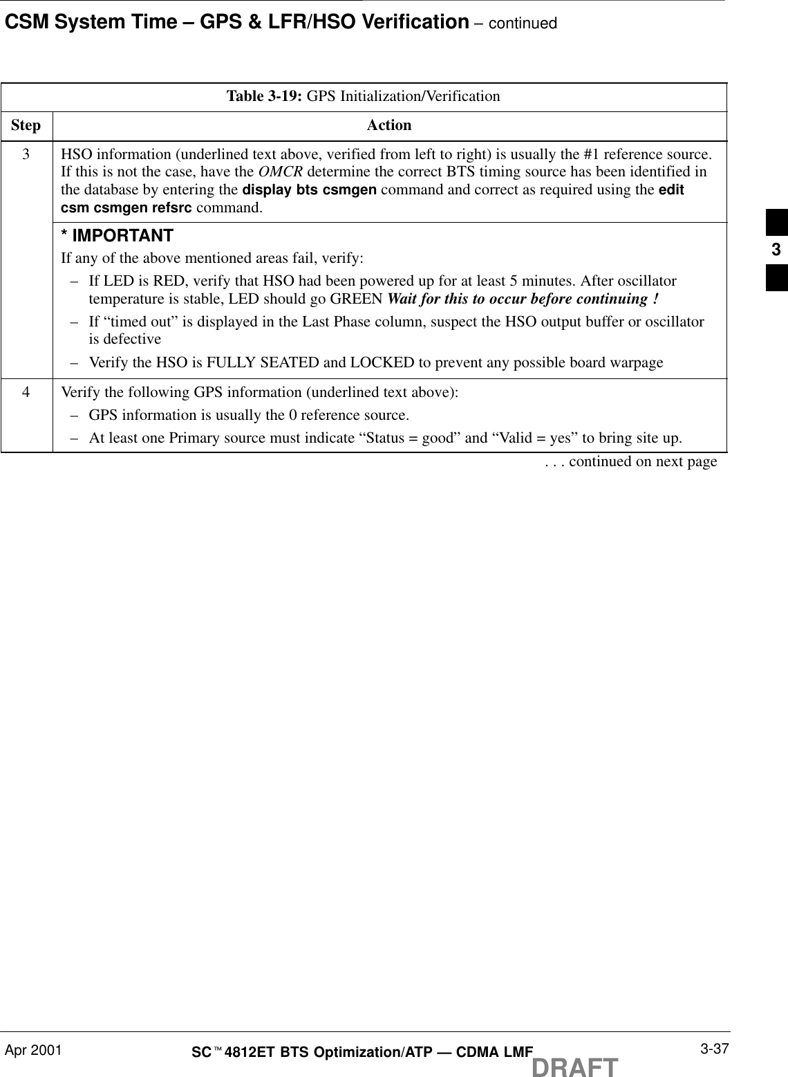
CSM System Time – GPS & LFR/HSO Verification – continuedApr 2001 3-37SCt4812ET BTS Optimization/ATP — CDMA LMFDRAFTTable 3-19: GPS Initialization/VerificationStep Action3HSO information (underlined text above, verified from left to right) is usually the #1 reference source.If this is not the case, have the OMCR determine the correct BTS timing source has been identified inthe database by entering the display bts csmgen command and correct as required using the editcsm csmgen refsrc command.* IMPORTANTIf any of the above mentioned areas fail, verify:–If LED is RED, verify that HSO had been powered up for at least 5 minutes. After oscillatortemperature is stable, LED should go GREEN Wait for this to occur before continuing !– If “timed out” is displayed in the Last Phase column, suspect the HSO output buffer or oscillatoris defective–Verify the HSO is FULLY SEATED and LOCKED to prevent any possible board warpage4Verify the following GPS information (underlined text above):–GPS information is usually the 0 reference source.–At least one Primary source must indicate “Status = good” and “Valid = yes” to bring site up.. . . continued on next page3
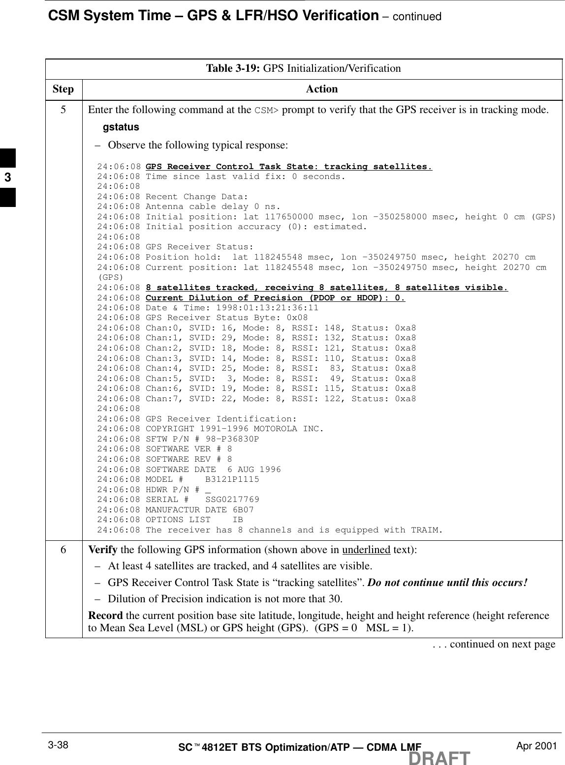
CSM System Time – GPS & LFR/HSO Verification – continuedDRAFTSCt4812ET BTS Optimization/ATP — CDMA LMF Apr 20013-38Table 3-19: GPS Initialization/VerificationStep Action5Enter the following command at the CSM> prompt to verify that the GPS receiver is in tracking mode.gstatus–Observe the following typical response:24:06:08 GPS Receiver Control Task State: tracking satellites.24:06:08 Time since last valid fix: 0 seconds.24:06:08 24:06:08 Recent Change Data:24:06:08 Antenna cable delay 0 ns.24:06:08 Initial position: lat 117650000 msec, lon –350258000 msec, height 0 cm (GPS)24:06:08 Initial position accuracy (0): estimated.24:06:08 24:06:08 GPS Receiver Status:24:06:08 Position hold:  lat 118245548 msec, lon –350249750 msec, height 20270 cm24:06:08 Current position: lat 118245548 msec, lon –350249750 msec, height 20270 cm(GPS)24:06:08 8 satellites tracked, receiving 8 satellites, 8 satellites visible.24:06:08 Current Dilution of Precision (PDOP or HDOP): 0.24:06:08 Date & Time: 1998:01:13:21:36:1124:06:08 GPS Receiver Status Byte: 0x0824:06:08 Chan:0, SVID: 16, Mode: 8, RSSI: 148, Status: 0xa824:06:08 Chan:1, SVID: 29, Mode: 8, RSSI: 132, Status: 0xa824:06:08 Chan:2, SVID: 18, Mode: 8, RSSI: 121, Status: 0xa824:06:08 Chan:3, SVID: 14, Mode: 8, RSSI: 110, Status: 0xa824:06:08 Chan:4, SVID: 25, Mode: 8, RSSI:  83, Status: 0xa824:06:08 Chan:5, SVID:  3, Mode: 8, RSSI:  49, Status: 0xa824:06:08 Chan:6, SVID: 19, Mode: 8, RSSI: 115, Status: 0xa824:06:08 Chan:7, SVID: 22, Mode: 8, RSSI: 122, Status: 0xa824:06:08 24:06:08 GPS Receiver Identification:24:06:08 COPYRIGHT 1991–1996 MOTOROLA INC. 24:06:08 SFTW P/N # 98–P36830P      24:06:08 SOFTWARE VER # 8           24:06:08 SOFTWARE REV # 8           24:06:08 SOFTWARE DATE  6 AUG 1996 24:06:08 MODEL #    B3121P1115      24:06:08 HDWR P/N # _               24:06:08 SERIAL #   SSG0217769      24:06:08 MANUFACTUR DATE 6B07       24:06:08 OPTIONS LIST    IB        24:06:08 The receiver has 8 channels and is equipped with TRAIM.6Verify the following GPS information (shown above in underlined text):–At least 4 satellites are tracked, and 4 satellites are visible.–GPS Receiver Control Task State is “tracking satellites”. Do not continue until this occurs!–Dilution of Precision indication is not more that 30.Record the current position base site latitude, longitude, height and height reference (height referenceto Mean Sea Level (MSL) or GPS height (GPS).  (GPS = 0   MSL = 1).. . . continued on next page3
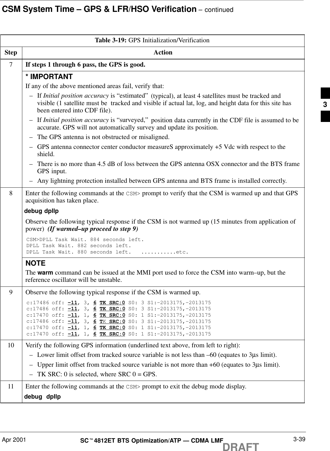
CSM System Time – GPS & LFR/HSO Verification – continuedApr 2001 3-39SCt4812ET BTS Optimization/ATP — CDMA LMFDRAFTTable 3-19: GPS Initialization/VerificationStep Action7If steps 1 through 6 pass, the GPS is good.* IMPORTANTIf any of the above mentioned areas fail, verify that:– If Initial position accuracy is “estimated” (typical), at least 4 satellites must be tracked andvisible (1 satellite must be  tracked and visible if actual lat, log, and height data for this site hasbeen entered into CDF file).– If Initial position accuracy is “surveyed,” position data currently in the CDF file is assumed to beaccurate. GPS will not automatically survey and update its position.–The GPS antenna is not obstructed or misaligned.–GPS antenna connector center conductor measureS approximately +5 Vdc with respect to theshield.–There is no more than 4.5 dB of loss between the GPS antenna OSX connector and the BTS frameGPS input.–Any lightning protection installed between GPS antenna and BTS frame is installed correctly.8Enter the following commands at the CSM> prompt to verify that the CSM is warmed up and that GPSacquisition has taken place.debug dpllp Observe the following typical response if the CSM is not warmed up (15 minutes from application ofpower)  (If warmed–up proceed to step 9)CSM>DPLL Task Wait. 884 seconds left.DPLL Task Wait. 882 seconds left.DPLL Task Wait. 880 seconds left.   ...........etc.NOTEThe warm command can be issued at the MMI port used to force the CSM into warm–up, but thereference oscillator will be unstable.9Observe the following typical response if the CSM is warmed up.c:17486 off: –11, 3, 6 TK SRC:0 S0: 3 S1:–2013175,–2013175c:17486 off: –11, 3, 6 TK SRC:0 S0: 3 S1:–2013175,–2013175c:17470 off: –11, 1, 6 TK SRC:0 S0: 1 S1:–2013175,–2013175c:17486 off: –11, 3, 6 TK SRC:0 S0: 3 S1:–2013175,–2013175c:17470 off: –11, 1, 6 TK SRC:0 S0: 1 S1:–2013175,–2013175c:17470 off: –11, 1, 6 TK SRC:0 S0: 1 S1:–2013175,–201317510 Verify the following GPS information (underlined text above, from left to right):–Lower limit offset from tracked source variable is not less than –60 (equates to 3µs limit).–Upper limit offset from tracked source variable is not more than +60 (equates to 3µs limit).–TK SRC: 0 is selected, where SRC 0 = GPS.11 Enter the following commands at the CSM> prompt to exit the debug mode display.debug  dpllp 3
CSM System Time – GPS & LFR/HSO Verification – continuedDRAFTSCt4812ET BTS Optimization/ATP — CDMA LMF Apr 20013-40LORAN–CInitialization/VerificationTable 3-20: LORAN–C Initialization/VerificationStep Action Note1At the CSM> prompt, enter lstatus <cr> to verify that the LFR is in trackingmode.  A typical response is:CSM> lstatus <cr>LFR St ti St tLFR Station Status:Clock coherence: 512 >5930M 51/60 dB 0 S/N Flag:5930X 52/64 dn –1 S/N Flag:5990 47/55 dB –6 S/N Flag:7980M 62/66 dB 10 S/N FlThis must be greaterthan 100 before LFRbecomes a valid source.7980M 62/66 dB 10 S/N Flag:7980W 65/69 dB 14 S/N Flag: . PLL Station . >7980X 48/54 dB –4 S/N Flag:7980Y 46/58 dB –8 S/N Flag:E7980Z 60/67 dB 8 S/N Flag:8290M 50/65 dB 0 S/N FlagThis shows the LFR islocked to the selectedPLL station.8290M 50/65 dB 0 S/N Flag:8290W 73/79 dB 20 S/N Flag:8290W 58/61 dB 6 S/N Flag:8290W 58/61 dB 6 S/N Flag:8970M 89/95 dB 29 S/N Flag:8970W 62/66 dB 10 S/N Flag:8970X 73/79 dB 22 S/N Flag:8970X 73/79 dB 22 S/N Flag:8970Y 73/79 dB 19 S/N Flag:8970Z 62/65 dB 10 S/N Flag:9610M 62/65 dB 10 S/N Flg9610M 62/65 dB 10 S/N Flag:9610V 58/61 dB 8 S/N Flag:9610W 47/49 dB –4S/N Flag:E9610W 47/49 dB –4 S/N Flag:E9610X 46/57 dB –5 S/N Flag:E9610Y 48/54 dB –5 S/N Flag:E9610Z 65/69 dB 12 S/N Flag9610Z 65/69 dB 12 S/N Flag:9940M 50/53 dB –1 S/N Flag:S9940W 49/56 dB –4 S/N Flag:E9940W 49/56 dB 4 S/N Flag:E9940Y 46/50 dB–10 S/N Flag:E9960M 73/79 dB 22 S/N Flag:9960W 51/60 dB 0 S/N Flag:9960W 51/60 dB 0 S/N Flag:9960X 51/63 dB –1 S/N Flag:9960Y 59/67 dB 8 S/N Flag:9960Z 89/96 dB 29 S/N Fl9960Z 89/96 dB 29 S/N Flag:LFR Task State: lfr locked to station 7980WLFR Recent Change Data:Search List: 5930 5990 7980 8290 8970 9940 9610 9960 >PLL GRI: 7980WLFR Master, reset not needed, not the reference source.CSM>This search list and PLLdata must match theconfiguration for thegeographical locationof the cell site.. . . continued on next page3
CSM System Time – GPS & LFR/HSO Verification – continuedApr 2001 3-41SCt4812ET BTS Optimization/ATP — CDMA LMFDRAFTTable 3-20: LORAN–C Initialization/VerificationStep NoteAction2Verify the following LFR information (highlighted above in boldface type):–Locate the “dot” that indicates the current phase locked station assignment (assigned by MM).–Verify that the station call letters are as specified in site documentation as well as M X Y Zassignment.–Verify the S/N ratio of the phase locked station is greater than 8.3At the CSM> prompt, enter sources <cr> to display the current status of the the LORAN receiver.–Observe the following typical response.Num Source Name Type TO Good Status Last Phase Target Phase Valid––––––––––––––––––––––––––––––––––––––––––––––––––––––––––––––––––––––––––––0 Local GPS Primary 4 Yes Good –3 0 Yes1 LFR ch A Secondary 4 Yes Good –2013177 –2013177 Yes2 Not usedCurrent reference source number: 14LORAN LFR information (highlighted above in boldface type) is usually the #1 reference source(verified from left to right).* IMPORTANTIf any of the above mentioned areas fail, verify:–The LFR antenna is not obstructed or misaligned.–The antenna pre–amplifier power and calibration twisted pair connections are intact and < 91.4 m(300 ft) in length.–A dependable connection to suitable Earth Ground is in place.–The search list and PLL station for cellsite location are correctly configured .NOTELFR functionality should be verified using the “source” command (as shown in Step 3).  Use theunderlined responses on the LFR row to validate correct LFR operation.5Close the hyperterminal window. 3
Test Equipment Set–upDRAFTSCt4812ET BTS Optimization/ATP — CDMA LMF Apr 20013-42Connecting Test Equipment tothe BTSAll test equipment is controlled by the LMF via IEEE–488/GPIB bus.The LMF requires each piece of test equipment to have a factory setGPIB address. If there is a communications problem between the LMFand any piece of test equipment, verify that the GPIB addresses havebeen set correctly (normally 13 for a power meter and 18 for a CDMAanalyzer).The following test equipment is required to perform optimization,calibration and ATP tests:SLMFSTest setSDirectional coupler and attenuatorSRF cables and connectorsRefer to Table 3-21 for an overview of connections for test equipmentcurrently supported by LMF. In addition, see the following figures:SFigure 3-9 and Figure 3-10 show the test set connections for TXcalibrationSFigure 3-11 and Figure 3-12 show the test set connections foroptimization/ATP testsSupported Test SetsOptimization and ATP testing may be performed using one of thefollowing test sets:SCyberTestSAdvantest R3465 and HP–437B or Gigatronics Power MeterSHewlett–Packard HP 8935SHewlett–Packard HP 8921 (W/CDMA and PCS Interface (1.9 GHz)and HP–437B or Gigatronics Power MeterSSpectrum Analyzer (HP8594E) – optionalSRubidium Standard Timebase – optionalTo prevent damage to the test equipment, all TX testconnections must be through the 30 dB directional couplerfor an 800 MHz BTS and the 30 dB directional couplerplus a 20 dB in-line attenuator for a 1.9 GHz BTS.CAUTION3
Test Equipment Set–up – continuedApr 2001 3-43SCt4812ET BTS Optimization/ATP — CDMA LMFDRAFTTest Equipment Setup ChartTable 3-21 depicts the current test equipment available meeting Motorolastandards.To identify the connection ports, locate the test equipment presentlybeing used in the TEST SETS columns, and read down the column.Where a ball appears in the column, connect one end of the test cable tothat port. Follow the horizontal line to locate the end connection(s),reading up the column to identify the appropriate equipment/BTS port.Table 3-21: Test Equipment SetupTEST SETS ADDITIONAL TEST EQUIPMENTSIGNAL Cyber–Test Ad-vantest HP8935 HP8921AHP8921W/PCS PowerMeterGPIBInter-face LMF DirectionalCoupler & Pad* BTSEVEN SECOND SYNCHRONIZATION EVENSEC REF EVEN SECSYNC INEVENSECONDSYNC INEVENSECONDSYNC INEVENSECONDSYNC IN19.6608 MHZCLOCK TIMEBASE INCDMATIME BASEIN EXTREF INCDMATIME BASEINCDMATIME BASEINCONTROLIEEE 488 BUS IEEE488 GPIB HP–IB HP–IB GPIB SERIALPORTHP–IB HP–IBTX TESTCABLES RFIN/OUT INPUT50–OHM RFIN/OUT TX1–6RFIN/OUT RFIN/OUT 20 DBPAD BTSPORTRX TESTCABLES RF IN/OUT RF OUT50–OHM DUPLEX RX1–12DUPLEXOUT RF OUTONLYSYNCMONITORFREQMONITOR3
Test Equipment Set–up  – continuedDRAFTSCt4812ET BTS Optimization/ATP — CDMA LMF Apr 20013-44Equipment Warm-upWarm-up BTS equipment for a minimum of 60 minutesprior to performing the BTS optimization procedure. Thisassures BTS site stability and contributes to optimizationaccuracy. (Time spent running initial power-up,hardware/firmware audit, and BTS download counts aswarm-up time.)IMPORTANT*Before installing any test equipment directly to any BTSTX OUT connector, verify there are NO CDMA BBXchannels keyed. At active sites, have the OMC-R/CBSCplace the antenna (sector) assigned to the LPA under testOOS. Failure to do so can result in serious personal injuryand/or equipment damage.WARNINGCable Calibration SetupFigure 3-8 shows the cable calibration setup for various supported testsets. The left side of the diagram depicts the location of the input andoutput ports of each test set, and the right side details the set up for eachtest. Table 3-25 provides a procedure for calibrating cables.3
Test Equipment Set–up – continuedApr 2001 3-45SCt4812ET BTS Optimization/ATP — CDMA LMFDRAFTMotorola CyberTestHewlett–Packard Model HP 8935Advantest Model R3465DUPLEXOUTRF OUT50–OHMINPUT50–OHMRF GEN OUTANT INANTINSUPPORTED TEST SETS100–WATT  (MIN)NON–RADIATINGRF LOADTESTSETA. SHORT CABLE CALSHORTCABLEB. RX TEST SETUPTESTSETC. TX TEST SETUP20 DB PADFOR 1.9 GHZCALIBRATION SET UPN–N FEMALEADAPTERTXCABLETXCABLESHORTCABLENote: The Directional Coupler is not used with theCybertest Test Set. The TX cable is connecteddirectly to the Cybertest Test Set.A 10dB attenuator must be used with the short testcable for cable calibration with the CyberTest TestSet. The 10dB attenuator is used only for the cablecalibration procedure, not with the test cables forTX calibration and ATP tests.TESTSETRXCABLESHORTCABLEFigure 3-8: Cable Calibration Test SetupFW00089Note: For 800 MHZ only. The HP8921A cannotbe used to calibrate cables for PCS frequencies.Hewlett–Packard Model HP 8921ADIRECTIONAL COUPLER (30 DB)N–N FEMALEADAPTER3
Test Equipment Set–up  – continuedDRAFTSCt4812ET BTS Optimization/ATP — CDMA LMF Apr 20013-46Setup for TX CalibrationFigure 3-9 and Figure 3-10 show the test set connections for TXcalibration.Motorola CyberTestHewlett–Packard Model HP 8935TEST SETS TRANSMIT (TX) SET UPFRONT PANEL RFIN/OUTRF IN/OUTHP–IBTO GPIBBOXRS232–GPIBINTERFACE BOXINTERNAL PCMCIAETHERNET CARDGPIBCABLECOMMUNICATIONSTEST SETCONTROLIEEE 488GPIB BUSUNIVERSAL TWISTEDPAIR (UTP) CABLE(RJ45 CONNECTORS)RS232NULLMODEMCABLEOUTS MODEDATA FORMATBAUD RATEGPIB ADRSG MODEONTEST SETINPUT/OUTPUTPORTSBTS100–WATT  (MIN)NON–RADIATINGRF LOADINTXTESTCABLECDMALMFDIP SWITCHSETTINGS**2O DB PADFOR 1.9 GHZ10BASET/10BASE2CONVERTERLANBLANATX TESTCABLETX ANTENNAPORT OR TXRFDSDIRECTIONALCOUPLERSPOWERMETER(OPTIONAL)*NOTE: THE DIRECTIONAL COUPLER IS NOT USED WITH THECYBERTEST TEST SET. THE TX CABLE IS CONNECTED DIRECTLYTO THE CYBERTEST TEST SET.* A POWER METER CAN BE USED IN PLACEOF THE COMMUNICATIONS TEST SET FOR TXCALIBRATION/AUDITPOWERSENSORFigure 3-9: TX Calibration Test Setup (CyberTest and HP 8935)FW00094DIRECTIONAL COUPLER(30 DB)** BLACK PORTION OF THEDIAGRAM REPRESENTS THERAISED PART OF THESWITCH3
Test Equipment Set–up – continuedApr 2001 3-47SCt4812ET BTS Optimization/ATP — CDMA LMFDRAFTPOWER METERTEST SETS TRANSMIT (TX) SET UPRS232–GPIBINTERFACE BOXINTERNAL PCMCIAETHERNET CARDGPIBCABLEUNIVERSAL TWISTEDPAIR (UTP) CABLE(RJ45 CONNECTORS)RS232NULLMODEMCABLES MODEDATA FORMATBAUD RATEGPIB ADRS G MODEONBTS100–WATT  (MIN)NON–RADIATINGRF LOADTXTESTCABLECDMALMFDIP SWITCHSETTINGS*2O DB PADFOR 1.9 GHZ10BASET/10BASE2CONVERTERLANBLANATX ANTENNA GROUPOR TX RFDS DIRECTIONALCOUPLERSTXTESTCABLEPOWERSENSORFW00095NOTE: THE HP8921A AND ADVANTESTCANNOT BE USED FOR TX CALIBRATION. APOWER METER MUST BE USED.Figure 3-10: TX Calibration Test Setup HP 8921A and AdvantestDIRECTIONAL COUPLER(30 DB)* BLACK PORTION OF THEDIAGRAM REPRESENTS THERAISED PART OF THESWITCH3
Test Equipment Set–up  – continuedDRAFTSCt4812ET BTS Optimization/ATP — CDMA LMF Apr 20013-48Setup for Optimization/ATPFigure 3-11 and Figure 3-12 show the test set connections foroptimization/ATP tests.Motorola CyberTestHewlett–Packard Model HP 8935DUPLEX OUTTEST SETS Optimization/ATP SET UPRFIN/OUTSYNC MONITOREVEN SEC TICKPULSE REFERENCEFROM CSM BOARDFREQ MONITOR19.6608 MHZ CLOCKREFERENCE FROMCSM BOARDRF IN/OUTHP–IBTO GPIBBOXAdvantest Model R3465INPUT50–OHMGPIB CONNECTSTO BACK OF UNITNOTE: The Directional Coupler is not usedwith the Cybertest Test Set. The TX cable isconnected directly to the Cybertest Test set.RF OUTRX ANTENNAPORT OR RFDSRX ANTENNADIRECTIONALCOUPLERTX ANTENNAPORT OR RFDSRX ANTENNADIRECTIONALCOUPLERRS232–GPIBINTERFACE BOXINTERNAL PCMCIAETHERNET CARDGPIBCABLEUNIVERSAL TWISTEDPAIR (UTP) CABLE(RJ45 CONNECTORS)RS232 NULLMODEMCABLES MODEDATA FORMATBAUD RATEGPIB ADRS G MODEONBTSTXTESTCABLECDMALMFDIPSWITCH SETTINGS*10BASET/10BASE2CONVERTERLANBLANARXTESTCABLECOMMUNICATIONSTEST SETIEEE 488GPIB BUSINTEST SETINPUT/OUTPUTPORTSOUTNOTE:  IF BTS RX/TX SIGNALS AREDUPLEXED (4800E): BOTH THE TX AND RXTEST CABLES CONNECT TO THE DUPLEXEDANTENNA GROUP.100–WATT  (MIN)NON–RADIATINGRF LOAD2O DB PADFOR 1.9 GHZDIRECTIONALCOUPLER(30 DB)EVENSECOND/SYNCIN (BNC “T”WITH 50 OHMTERMINATOR)CDMATIMEBASE INFREQMONITORSYNCMONITORCSMFW00096Figure 3-11: Optimization/ATP Test Setup Calibration (CyberTest, HP 8935 and Advantest)SYNC MONITOREVEN SEC TICKPULSE REFERENCEFROM CSM BOARDFREQ MONITOR19.6608 MHZ CLOCKREFERENCE FROMCSM BOARDSYNC MONITOREVEN SEC TICKPULSE REFERENCEFROM CSM BOARDFREQ MONITOR19.6608 MHZ CLOCKREFERENCE FROMCSM BOARDRFOUT* BLACK PORTION OF THEDIAGRAM REPRESENTS THERAISED PART OF THESWITCH3
Test Equipment Set–up – continuedApr 2001 3-49SCt4812ET BTS Optimization/ATP — CDMA LMFDRAFTRF OUTONLYHewlett–Packard Model HP 8921A W/PCS Interface(for  1700 and 1900 MHz)HP PCSINTERFACE*GPIBCONNECTSTO BACK OFUNITSSYNC MONITOREVEN SEC TICKPULSE REFERENCEFROM CSM BOARDFREQ MONITOR19.6608 MHZ CLOCKREFERENCE FROMCSM BOARDTEST SETS Optimization/ATP SET UPRX ANTENNAPORT OR RFDSRX ANTENNADIRECTIONALCOUPLERTX ANTENNAPORT OR RFDSRX ANTENNADIRECTIONALCOUPLERRS232–GPIBINTERFACE BOXINTERNAL PCMCIAETHERNET CARDGPIBCABLEUNIVERSAL TWISTEDPAIR (UTP) CABLE(RJ45 CONNECTORS)RS232 NULLMODEMCABLES MODEDATA FORMATBAUD RATEGPIB ADRS G MODEONBTSTXTESTCABLECDMALMFDIPSWITCH SETTINGS*10BASET/10BASE2CONVERTERLANBLANARXTESTCABLECOMMUNICATIONSTEST SETIEEE 488GPIB BUSINTEST SETINPUT/OUTPUTPORTSOUTNOTE:  IF BTS RX/TX SIGNALS AREDUPLEXED (4800E): BOTH THE TX AND RXTEST CABLES CONNECT TO THE DUPLEXEDANTENNA GROUP.100–WATT  (MIN)NON–RADIATINGRF LOAD2O DB PADFOR 1.9 GHZEVENSECOND/SYNCIN (BNC “T”WITH 50 OHMTERMINATOR)CDMATIMEBASE INFREQMONITORSYNCMONITORCSMRFIN/OUTFigure 3-12: Optimization/ATP Test Setup HP 8921AREF FW00097GPIBCONNECTSTO BACK OFUNITSYNC MONITOREVEN SEC TICKPULSE REFERENCEFROM CSM BOARDFREQ MONITOR19.6608 MHZ CLOCKREFERENCE FROMCSM BOARDHewlett–Packard Model HP 8921A(for 800 MHz)* FOR 1700 AND1900 MHZ ONLYDIRECTIONALCOUPLER(30 DB)RFIN/OUTRF OUTONLY* BLACK PORTION OF THEDIAGRAM REPRESENTS THERAISED PART OF THESWITCH3
Test Set CalibrationDRAFTSCt4812ET BTS Optimization/ATP — CDMA LMF Apr 20013-50BackgroundProper test equipment setup ensures that the test equipment andassociated test cables do not introduce measurement errors, and thatmeasurements are correct.If the test set being used to interface with the BTS has beencalibrated and maintained as a set, this procedure does notneed to be performed. (Test Set includes LMF terminal,communications test set, additional test equipment,associated test cables, and adapters.)NOTEThis procedure must be performed prior to beginning the optimization.Verify all test equipment (including all associated test cables andadapters actually used to interface all test equipment and the BTS) hasbeen calibrated and maintained as a set.If any piece of test equipment, test cable, or RF adapter,that makes up the calibrated test equipment set, has beenreplaced, re-calibration must be performed. Failure to do socan introduce measurement errors, resulting in incorrectmeasurements and degradation to system performance.CAUTIONCalibration of the communications test set (or equivalenttest equipment) must be performed at the site beforecalibrating the overall test set. Calibrate the test equipmentafter it has been allowed to warm–up and stabilize for aminimum of 60 minutes.IMPORTANT*PurposeThese procedures access the CDMA LMF automated calibration routineused to determine the path losses of the supported communicationsanalyzer, power meter, associated test cables, and (if used) antennaswitch that make up the overall calibrated test set. After calibration, thegain/loss offset values are stored in a test measurement offset file on theCDMA LMF.3
Test Set Calibration – continuedDRAFTApr 2001 3-51SCt4812ET BTS Optimization/ATP — CDMA LMFSelecting Test EquipmentUse LMF Options from the Options menu list to select test equipmentautomatically (using the autodetect feature) or manually.PrerequisitesA Serial Connection and a Network Connection tab are provided fortest equipment selection. The Serial Connection tab is used when thetest equipment items are connected directly to the CDMA LMFcomputer via a GPIB box (normal setup). The Network Connection tabis used when the test equipment is to be connected remotely via anetwork connection.Ensure the following has been completed before selecting testequipment:STest equipment is correctly connected and turned on.SCDMA LMF computer serial port and test equipment are connected tothe GPIB box.Manually Selecting TestEquipment in a SerialConnection TabTest equipment can be manually specified before, or after, the testequipment is connected. CDMA LMF does not check to see if the testequipment is actually detected for manual specification.Table 3-22: Selecting Test Equipment Manually in a Serial Connection TabStep Action1From the Options menu, select LMF Options. The LMF Options window appears.2Click on the Serial Connection tab (if not in the forefront).3Select the correct serial port in the COMM Port pick list (normally COM1).4Click on the Manual Specification button (if not enabled).5Click on the check box corresponding to the test item(s) to be used.6Type the GPIB address in the corresponding GPIB address box. Recommended Addresses13=Power Meter18=CDMA Analyzer7Click on Apply. (The button will darken until the selection has been committed.)NOTEWith manual selection, CDMA LMF does not detect the test equipment to see if it is connected andcommunicating with CDMA LMF.8Click on Dismiss to close the test equipment window.3
Test Set Calibration – continuedDRAFTSCt4812ET BTS Optimization/ATP — CDMA LMF Apr 20013-52Automatically Selecting TestEquipment in a SerialConnection Tab When using the auto-detection feature to select test equipment, theCDMA LMF examines which test equipment items are actuallycommunicating with CDMA LMF. Follow the procedure in Table 3-23to use the auto-detect feature.Table 3-23: Selecting Test Equipment Using Auto-DetectStep Action1From the Options menu, select LMF Options. The LMF Options window appears.2Click on the Serial Connection tab (if not in the forefront).3Select the correct serial port in the COMM Port pick list (normally COM1).4Click on Auto–Detection (if not enabled).5Type in the GPIB addresses in the box labeled GPIB address to search (if not already displayed).NOTEWhen both a power meter and analyzer are selected, the first item listed in the GPIB addresses tosearch box will be used for RF power measurements (i.e., TX calibration). The address for a powermeter is normally 13 and the address for a CDMA analyzer is normally 18. If 13,18 is included in theGPIB addresses to search box, the power meter (13) will be used for RF power measurements. If thetest equipment items are manually selected the CDMA analyzer is used only if a power meter is notselected.6 Click Apply.  The button will darken until the selection has been committed. A check mark willappear in the Manual Configuration section for detected test equipment items.7 Click Dismiss to close the LMF Options window.3
Test Set Calibration – continuedDRAFTApr 2001 3-53SCt4812ET BTS Optimization/ATP — CDMA LMFCalibrating Test EquipmentThe calibrate test equipment function zeros the power measurement levelof the test equipment item that is to be used for TX calibration and audit.If both a power meter and an analyzer are connected, only the powermeter is zeroed.Calibrate Test Equipment from the Util menu list is used to calibratetest equipment item before being used for testing. The test equipmentmust be selected before beginning calibration. Follow the procedure inTable 3-24 to calibrate the test equipment.Table 3-24: Test Equipment CalibrationStep Action1From the Util menu, select Calibrate Test Equipment. A Directions window is displayed. Followthe instructions provided.2Follow the direction provided.3Click on Continue to close the Directions window. A status window is displayed.4Click on OK to close the status report window.Calibrating CablesThe cable calibration function is used to measure the loss (in dB) for theTX and RX cables that are to be used for testing. A CDMA analyzer isused to measure the loss of each cable configuration (TX cableconfiguration and RX cable configuration). The cable calibrationconsists of the following steps.SMeasure the loss of a short cable. This is done to compensate for anymeasurement error of the analyzer. The short cable, which is used onlyfor the calibration process, is used in series with both the TX and RXcable configuration when they are measured. The measured loss of theshort cable is deducted from the measured loss of the TX and RXcable configuration to determine the actual loss of the TX and RXcable configurations. This deduction is done so any error in theanalyzer measurement will be adjusted out of both the TX and RXmeasurements.SThe short cable plus the RX cable configuration loss is measured. TheRX cable configuration normally consists only of a coax cable withtype–N connectors that is long enough to reach from the BTS RX portthe test equipment.SThe short cable plus the TX cable configuration loss is measured. TheTX cable configuration normally consists of two coax cables withtype–N connectors and a directional coupler, a load, and an additionalattenuator if required by the BTS type. The total loss of the path lossof the TX cable configuration must be as required for the BTS(normally 30 or 50 dB). The Motorola Cybertest analyzer is differentin that the required attenuation/load is built into the test set so the TXcable configuration consists only of the required length coax cable.3
Test Set Calibration – continuedDRAFTSCt4812ET BTS Optimization/ATP — CDMA LMF Apr 20013-54Calibrating Cables with aCDMA AnalyzerThe Cable Calibration menu item from the Util menu list is used tocalibrate both TX and RX test cables for use with CDMA LMF.LMF cable calibration cannot be accomplished with anHP8921A analyzer for 1.9 MHz. A different analyzer typeor the signal generator and spectrum analyzer method mustbe used (refer to Table 3-26 and Table 3-27). Cablecalibration values must be manually entered if the signalgenerator and spectrum analyzer method is used. For theHP8921A, refer to Appendix F.NOTEThe test equipment must be selected before this procedure can be started.Follow the procedure in Table 3-25 to calibrate the cables. Figure 3-8illustrates the cable calibration test equipment setup.Table 3-25: Cable CalibrationStep Action1From the Util menu, select Cable Calibration. A Cable Calibration window is displayed.2Enter a channel number(s) in the Channels box. Multiple channels numbers must be separated with acomma, no space (i.e., 200,800). When two or more channels numbers are entered, the cables will becalibrated for each channel. Interpolation will be accomplished for other channels as required for TXcalibration.3 Select TX and RX CABLE CAL, TX CABLE CAL or RX CABLE CAL in the Cable Calibrationpicklist.4 Click OK. Follow the directions displayed for each step. A status report window will be displayedwith the results of the cable calibration. 3
Test Set Calibration – continuedDRAFTApr 2001 3-55SCt4812ET BTS Optimization/ATP — CDMA LMFCalibrating TX Cables Using aSignal Generator andSpectrum AnalyzerFollow the procedure in Table 3-26 to calibrate the TX cables using thesignal generator and spectrum analyzer. Refer to Figure 3-13 for adiagram of the signal generator and spectrum analyzer.Table 3-26: Calibrating TX Cables Using Signal Generator and Spectrum AnalyzerStep Action1Connect a short test cable between the spectrum analyzer and the signal generator.2Set signal generator to 0 dBm at the customer frequency of 1840–1870 MHz band for Korea PCS and1930–1990 MHz band for North American PCS.3Use spectrum analyzer to measure signal generator output (see Figure 3-13, “A”) and record the value.4Connect the spectrum analyzer’s short cable to point “B”, as shown in the lower portion of thediagram, to measure cable output at customer frequency (1840–1870 MHz for Korea PCS and1930–1990 MHz for North American PCS) and record the value at point “B”.5Calibration factor = A – B  Example:  Cal = –1 dBm – (–53.5 dBm) = 52.5 dBNOTEThe short cable is used for calibration only. It is not part of the final test setup. After calibration iscompleted, do not re-arrange any cables. Use the equipment setup, as is, to ensure test procedures usethe correct calibration factor.Figure 3-13:  Calibrating Test Equipment Setup for TX Cable Calibration(Using Signal Generator and Spectrum Analyzer)50 OHMTERMINATION30 DBDIRECTIONALCOUPLERSpectrumAnalyzerSignal GeneratorASpectrumAnalyzer40W NON–RADIATINGRF LOADBSHORT TEST CABLESignal GeneratorTHIS WILL BE THE CONNECTION TO THEPOWER METER DURING TX CALIBRATIONAND TO THE CDMA ANALYZER DURING TXATP TESTS.SHORTTESTCABLE THIS WILL BE THE CONNECTIONTO THE TX PORTS DURING TXCALIBRATION AND TO THE TX/RXPORTS DURING ATP TESTS.SECOND RFTEST CABLE.ONE 20DB 20 W INLINE ATTENUATORFW002933
Test Set Calibration – continuedDRAFTSCt4812ET BTS Optimization/ATP — CDMA LMF Apr 20013-56Calibrating RX Cables Using aSignal Generator andSpectrum Analyzer Follow the procedure in Table 3-27 to calibrate the RX cables using thesignal generator and spectrum analyzer. Refer to Figure 3-14, if required.Table 3-27: Calibrating RX Cables Using a Signal Generator and Spectrum AnalyzerStep Action1Connect a short test cable to the spectrum analyzer and connect the other end to the Signal Generator.2Set signal generator to –10 dBm at the customer’s RX frequency of 1750–1780 MHz for Korean PCSand 1850–1910 MHz band for North American PCS.3Use spectrum analyzer to measure signal generator output (see Figure 3-14, “A”) and record the valuefor “A”.4Connect the test setup, as shown in the lower portion of the diagram, to measure the output at thecustomer’s RX frequency in the 1850–1910 MHz band. Record the value at point ‘‘B”.5Calibration factor = A – BExample: Cal = –12 dBm – (–14 dBm) = 2 dBNOTEThe short test cable is used for test equipment setup calibration only. It is not be part of the final testsetup. After calibration is completed, do not re-arrange any cables. Use the equipment setup, as is, toensure test procedures use the correct calibration factor.Figure 3-14:  Calibrating Test Equipment Setup for RX ATP Test(Using Signal Generator and Spectrum Analyzer)SpectrumAnalyzerSignalGeneratorABSpectrumAnalyzerSHORTTESTCABLESHORT TESTCABLECONNECTION TO THE OUTPUTPORT DURING RX MEASUREMENTSSignalGeneratorBULLETCONNECTORLONGCABLE 2CONNECTION TO THE RX PORTSDURING RX MEASUREMENTS. FW002943
Test Set Calibration – continuedDRAFTApr 2001 3-57SCt4812ET BTS Optimization/ATP — CDMA LMFSetting Cable Loss Values Cable loss values for the TX and RX test cable configurations arenormally set by accomplishing cable calibration with use of theapplicable test equipment. The resulting values are stored in the cableloss files. The cable loss values can also be set/changed manually.PrerequisitesSLogged into the BTSTable 3-28: Setting Cable Loss ValuesStep Action1Click on the Util menu.2 Select Edit >Cable Loss > TX or RX. A data entry pop–up window will appear.3Click on the Add Row button to add a new channel number. Then click in the Channel # and Loss(dBm) columns and enter the desired values.4To edit existing values click in the data box to be changed and change the value.5To delete a row, click on the row and then click on the Delete Row button.6Click on the Save button to save displayed values.7Click on the Dismiss button to exit the window. Values that were entered/changed after the Savebutton was used will not be saved.NOTESIf cable loss values exist for two different channels the LMF will interpolate for all other channels.SEntered values will be used by the LMF as soon as they are saved. You do not have to logout andlogin.3
Test Set Calibration – continuedDRAFTSCt4812ET BTS Optimization/ATP — CDMA LMF Apr 20013-58Setting TX Coupler Loss Value If an in–service TX coupler is installed the coupler loss (e.g., 30 dB)must be manually entered so it will be included in the LMF TXcalibration and audit calculations.PrerequisitesSLogged into the BTSTable 3-29: Setting TX Coupler Loss ValuesStep Action1Click on the Util menu.2 Select Edit >TX Coupler Loss. A data entry pop–up window will appear.3Click in the Loss (dBm) column for each carrier that has a coupler and enter the appropriate value.4To edit existing values click in the data box to be changed and change the value.5Click on the Save button to save displayed values.6Click on the Dismiss button to exit the window. Values that were entered/changed after the Savebutton was used will not be saved.NOTESThe In–Service Calibration check box in the Options>LMF Options>BTS Options tab mustchecked before entered TX coupler loss values will be used by the TX calibration and auditfunctions.SEntered values will be used by the LMF as soon as they are saved. You do not have to logout andlogin.3
Bay Level Offset CalibrationApr 2001 3-59SCt4812ET BTS Optimization/ATP — CDMA LMFDRAFTIntroductionCalibration compensates for normal equipment variations within theBTS and assures maximum measurement accuracy.RF Path Bay Level OffsetCalibrationCalibration identifies the accumulated gain in every transmit path(BBX2 slot) at the BTS site and stores that value in the CAL file. TheBLOs are subsequently downloaded to each BBX2.Each receive path starts at a BTS RX antenna port and terminates at abackplane BBX2 slot. Each transmit path starts at a BBX2 backplaneslot, travels through the LPA, and terminates at a BTS TX antenna port.Calibration identifies the accumulated gain in every transmit path(BBX2 slot) at the BTS site and stores that value in the CAL file. Eachtransmit path starts at a C–CCP shelf backplane BBX2 slot, travelsthrough the LPA, and ends at a BTS TX antenna port. When the TX pathcalibration is performed, the RX path BLO will automatically be set tothe default value.When to Calibrate BLOs Calibration of BLOs is required after initial BTS installation.The BLO data of an operational BTS site must be re-calibrated onceeach year. Motorola recommends re-calibrating the BLO data for allassociated RF paths after replacing any of the following components orassociated interconnecting RF cabling:SBBX2 boardSC–CCP shelfSCIO cardSCIO to LPA backplane RF cableSLPA backplaneSLPASTX filter / TX filter combinerSTX thru-port cable to the top of frame3
Bay Level Offset Calibration – continuedDRAFTSCt4812ET BTS Optimization/ATP — CDMA LMF Apr 20013-60TX Path CalibrationThe TX Path Calibration assures correct site installation, cabling, and thefirst order functionality of all installed equipment. The proper functionof each RF path is verified during calibration. The external testequipment is used to validate/calibrate the TX paths of the BTS.Before installing any test equipment directly to any TXOUT connector you must first verify that there are noCDMA channels keyed. Have the OMC–R place the sectorassigned to the LPA under test OOS. Failure to do so canresult in serious personal injury and/or equipment damage.WARNINGAlways wear a conductive, high impedance wrist strapwhile handling any circuit card/module. If this is not done,there is a high probability that the card/module could bedamaged by ESD.CAUTIONAt new site installations, to facilitate the complete test ofeach CCP shelf (if the shelf is not already fully populatedwith BBX2 boards), move BBX2 boards from shelvescurrently not under test and install them into the emptyBBX2 slots of the shelf currently being tested to insure thatall BBX2 TX paths are tested.–This procedure can be bypassed on operational sitesthat are due for periodic optimization.–Prior to testing, view the CDF file to verify thecorrect BBX2 slots are equipped. Edit the file asrequired to include BBX2 slots not currentlyequipped (per Systems Engineering documentation).IMPORTANT*3
Bay Level Offset Calibration – continuedApr 2001 3-61SCt4812ET BTS Optimization/ATP — CDMA LMFDRAFTBLO Calibration Data FileDuring the calibration process, the LMF creates a calibration (BLO) datafile. After calibration has been completed, this offset data must bedownloaded to the BBX2s using the Download BLO function. Anexplanation of the file is shown below.Due to the size of the file, Motorola  recommends that youprint out a hard copy of a bts.cal file and refer to it for thefollowing descriptions.NOTEThe CAL file is subdivided into sections organized on a per slot basis (aslot Block).Slot 1 contains the calibration data for the 12 BBX2 slots. Slot 20contains the calibration data for the redundant BBX2 (see Table 3-31).Each BBX2 slot header block contains:SA creation Date and Time – broken down into separate parameters ofcreateMonth, createDay, createYear, createHour, and createMin.SThe number of calibration entries – fixed at 720 entries correspondingto 360 calibration points of the CAL file including the slot header andactual calibration data.SThe calibration data for a BBX2 is organized as a large flat array. Thearray is organized by branch, BBX2 slot, and calibration point.–The first breakdown of the array indicates which branch thecontained calibration points are for. The array covers transmit, mainreceive and diversity receive offsets as follows:Table 3-30: BLO BTS.cal file Array Branch AssignmentsRange AssignmentC[1]–C[240] TransmitC[241]–C[480] ReceiveC[481]–C[720] Diversity Receive3
Bay Level Offset Calibration – continuedDRAFTSCt4812ET BTS Optimization/ATP — CDMA LMF Apr 20013-62–The second breakdown of the array is per sector. Three sectors areallowed.Table 3-31: BTS.cal File Array (Per Sector)BBX2 Sectorization TX RX RX DiversitySlot[1] (Primary BBX2s 1 through 12)1 (Omni) 3–Sector, C[1]–C[20] C[241]–C[260] C[481]–C[500]23–Sector,1st C[21]–C[40] C[261]–C[280] C[501]–C[520]36 Sector, Carrier C[41]–C[60] C[281]–C[300] C[521]–C[540]41stCarrier 3–Sector, C[61]–C[80] C[301]–C[320] C[541]–C[560]5Carrier 3–Sector,3rd C[81]–C[100] C[321]–C[340] C[561]–C[580]6Carrier C[101]–C[120] C[341]–C[360] C[581]–C[600]73–Sector, C[121]–C[140] C[361]–C[380] C[601]–C[620]83–Sector,2nd C[141]–C[160] C[381]–C[400] C[621]–C[640]96 Sector, Carrier C[161]–C[180] C[401]–C[420] C[641]–C[660]10 2ndCarrier 3–Sector, C[181]–C[200] C[421]–C[440] C[661]–C[680]11 Carrier 3–Sector,4th C[201]–C[220] C[441]–C[460] C[681]–C[700]12 Carrier C[221]–C[240] C[461]–C[480] C[701]–C[720]Slot[20] (Redundant BBX2–13)1 (Omni) 3–Sector, C[1]–C[20] C[241]–C[260] C[481]–C[500]23–Sector,1st C[21]–C[40] C[261]–C[280] C[501]–C[520]36 Sector, Carrier C[41]–C[60] C[281]–C[300] C[521]–C[540]41stCarrier 3–Sector, C[61]–C[80] C[301]–C[320] C[541]–C[560]5Carrier 3–Sector,3rd C[81]–C[100] C[321]–C[340] C[561]–C[580]6Carrier C[101]–C[120] C[341]–C[360] C[581]–C[600]73–Sector, C[121]–C[140] C[361]–C[380] C[601]–C[620]83–Sector,2nd C[141]–C[160] C[381]–C[400] C[621]–C[640]96 Sector, Carrier C[161]–C[180] C[401]–C[420] C[641]–C[660]10 2ndCarrier 3–Sector, C[181]–C[200] C[421]–C[440] C[661]–C[680]11 Carrier 3–Sector,4th C[201]–C[220] C[441]–C[460] C[681]–C[700]12 Carrier C[221]–C[240] C[461]–C[480] C[701]–C[720]SRefer to the hard copy of the file. As you can see, 10 calibrationpoints per sector are supported for each branch. Two entries arerequired for each calibration point.SThe first value (all odd entries) refer to the CDMA channel(frequency) the BLO is measured at. The second value (all evenentries) is the power set level. The valid range for PwrLvlAdj is from2500 to 27500 (2500 corresponds to –125 dBm and 27500corresponds to +125 dBm).3
Bay Level Offset Calibration – continuedApr 2001 3-63SCt4812ET BTS Optimization/ATP — CDMA LMFDRAFTSThe 20 calibration entries for each slot/branch combination must bestored in order of increasing frequency. If less than 10 points(frequencies) are calibrated, the largest frequency that is calibrated isrepeated to fill out the 10 points.Example:C[1]=384, odd cal entry =   1 ‘‘calibration point”C[2]=19102, even cal entryC[3]=777,C[4]=19086,..C[19]=777,C[20]=19086, (since only two cal points were calibrated this would be repeated for the next 8 points)SWhen the BBX2 is loaded with BLO data, the cal file data for theBBX2 is downloaded to the device in the order it is stored in the CALfile. TxCal data is sent first, C[1] – C[60]. BBX2 slot 1’s 10calibration points are sent (C[1] – C[20]), followed by BBX2 slot 2’s10 calibration points (C[21] – C[40]), etc. The RxCal data is sent next,followed by the RxDCal data.STemperature compensation data is also stored in the cal file for eachslot.Test Equipment Setup:RF Path CalibrationFollow the steps outlined in Table 3-32 to set up test equipment.Table 3-32: Test Equipment Setup (RF Path Calibration)Step ActionNOTEVerify the GPIB is properly connected and turned on.! CAUTIONTo prevent damage to the test equipment, all transmit (TX) test connections must be via the 30 dBdirectional coupler for 800 MHz or via a 30 dB coupler with a 20 dB in–line attenuator for 1900 MHz.1Connect the LMF computer terminal to the BTS LAN A connector on the BTS (if you have notalready done so). Refer to the procedure in Table 3-6.SIf required, calibrate the test equipment per the procedure in Table 3-24.SConnect the test equipment as shown in Figure 3-9 and Figure 3-10.3
Bay Level Offset Calibration – continuedDRAFTSCt4812ET BTS Optimization/ATP — CDMA LMF Apr 20013-64Transmit (TX) Path CalibrationThe assigned channel frequency and power level (as measured at the topof the frame) for transmit calibration is derived from the site CDF file.For each BBX2, the channel frequency is specified in the ChannelListCDF file parameter and the power is specified in the SIFPilotPwrCDF file parameter for the sector associated with the BBX2 (locatedunder the ParentSECTOR field of the ParentCARRIER CDF fileparameter).The calibration procedure attempts to adjust the power to within +0.5 dBof the desired power. The calibration will pass if the error is less than+1.5 dB.The TX Bay Level Offset at sites WITHOUT the directional coupleroption, is approximately 42.0 dB ±3.0 dB.SAt sites WITHOUT RFDS option, BLO is approximately 42.0 dB ±4.0 dB. A typical example would be TX output powermeasured at BTS (36.0 dBm) minus the BBX2 TX output level(approximately –6.0 dBm) would equate to 42 dB BLO.The TX Bay Level Offset at sites WITH the directional coupler option,is approximately 41.4 dB ±3.0 dB. TX BLO = Frame Power Outputminus BBX2 output level.SExample: TX output power measured at RFDS TX coupler(39.4 dBm) minus the BBX TX output level (approximately–2.0 dBm) and RFDS directional coupler/cable (approximately–0.6 dBm) would equate to 41.4 dB BLO.The LMF Tests menu list items, TX Calibration and All Cal/Audit,perform the TX BLO Calibration test for a XCVR(s). The All Cal/Auditmenu item performs TX calibration, downloads BLO, and performs TXaudit if the TX calibration passes. All measurements are made throughthe appropriate TX output connector using the calibrated TX cable setup.PrerequisitesBefore running this test, ensure that the following have been done:SCSM–1,GLIs, MCCs, and BBX2s have correct code load and dataload.SPrimary CSM and MGLI are INS.SAll BBX2s are OOS_RAM.STest equipment and test cables are calibrated and connected for TXBLO calibration.SLMF is logged into the BTS.Connect the test equipment as shown in  Figure 3-9 and Figure 3-10 andfollow the procedure in Table 3-33 to perform the TX calibration test.3
Bay Level Offset Calibration – continuedApr 2001 3-65SCt4812ET BTS Optimization/ATP — CDMA LMFDRAFTBefore installing any test equipment directly to any TXOUT connector, first verify there are no CDMA BBX2channels keyed. Failure to do so can result in seriouspersonal injury and/or equipment damage.WARNINGVerify all BBX2 boards removed and repositioned havebeen returned to their assigned shelves/slots. Any BBX2boards moved since they were downloaded will have to bedownloaded again.IMPORTANT*Table 3-33: BTS TX Path CalibrationStep Action1Select the BBX2(s) to be calibrated.2From the Tests menu, select TX Calibration or All Cal/Audit.3Select the appropriate carrier(s) displayed in the Channels/Carrier pick list.Press and hold the <Shift> or <Ctrl> key to select multiple items.4Type the appropriate channel number in the Carrier n Channels box.5Click on OK.6Follow the cable connection directions as they are displayed.The test results will be displayed in the status report window.7Click on Save Results or Dismiss to close the status report window. Exception HandlingIn the event of a failure, the calibration procedure displays a FAILmessage in the status report window and provides information in theDescription field.Recheck the test setup and connection and re–run the test. If the tests failagain, note specifics about the failure, and refer to Chapter 6,Troubleshooting.Download BLO ProcedureAfter a successful TX path calibration, download the BLO calibrationfile data to the BBX2s. BLO data is extracted from the CAL file for theBTS and downloaded to the selected BBX2 devices.3
Bay Level Offset Calibration – continuedDRAFTSCt4812ET BTS Optimization/ATP — CDMA LMF Apr 20013-66If a successful All Cal/Audit was completed, thisprocedure does not need to be performed, as BLO isdownloaded as part of the All Cal/Audit.NOTEPrerequisitesEnsure the following prerequisites have been met before proceeding.SBBXs being downloaded are OOS–RAM (yellow).STX calibration successfully completedFollow the steps in Table 3-34 to download the BLO data to the BBX2s.Table 3-34: Download BLOStep Action1Select the BBX2(s) to be downloaded.2From the Device menu, select Download BLO.A status report window displays the result of the download.NOTESelected device(s) do not change color when BLO is downloaded.3 Click OK to close the status report window. 3
Bay Level Offset Calibration – continuedApr 2001 3-67SCt4812ET BTS Optimization/ATP — CDMA LMFDRAFTCalibration Audit IntroductionThe BLO calibration audit procedure confirms the successful generationand storage of the BLO calibrations. The calibration audit proceduremeasures the path gain or loss of every BBX2 transmit path at the site.In this test, actual system tolerances are used to determine the success orfailure of a test. The same external test equipment set up is used.*RF path verification, BLO calibration, and BLO datadownload to BBX2s must have been successfullycompleted prior to performing the calibration audit.IMPORTANTTransmit (TX) Path AuditPerform the calibration audit of the TX paths of all equipped BBX2slots, per the steps in Table 3-35.Before installing any test equipment directly to any TXOUT connector, first verify there are no CDMA BBX2channels keyed. Failure to do so can result in seriouspersonal injury and/or equipment damage.WARNINGIf a successful All Cal/Audit was completed, thisprocedure does not need to be performed, as BLO isdownloaded as part of the All Cal/Audit.NOTE3
Bay Level Offset Calibration – continuedDRAFTSCt4812ET BTS Optimization/ATP — CDMA LMF Apr 20013-68TX Audit TestThe Tests menu item, TX Audit, performs the TX BLO Audit test for aBBX2(s). All measurements are made through the appropriate TX outputconnector using the calibrated TX cable setup.PrerequisitesBefore running this test, the following should be done:SCSM–1,GLI2s, BBX2s have correct code load.SPrimary CSM and MGLI2 are INS.SAll BBX2s are OOS_RAM.STest equipment and test cables are calibrated and connected for TXBLO calibration.SLMF is logged into the BTS.Connect the test equipment as shown in Figure 3-9 and Figure 3-10 andfollow the procedure in Table 3-35 to perform the BTS TX Path Audittest.Table 3-35: TX Path AuditStep Action1Select the BBX2(s) to be audited. From the Tests menu, select TX Audit.2Select the appropriate carrier(s) displayed in the Channels/Carrier pick list.Press and hold the <Shift> or <Ctrl> key to select multiple items.3Type the appropriate channel number in the Carrier n Channels box.4Click on OK.5Follow the cable connection directions as they are displayed.A status report window displays the test results.6Click on Save Results or Dismiss to close the status report window. Exception HandlingIn the event of a failure, the calibration procedure displays a FAILmessage in the status report window and provides information in theDescription field.Recheck the test setup and connection and re–run the test. If the tests failagain, note specifics about the failure, and refer to Chapter 6,Troubleshooting.3
Bay Level Offset Calibration – continuedApr 2001 3-69SCt4812ET BTS Optimization/ATP — CDMA LMFDRAFTAll Cal/Audit TestThe Tests menu item, All Cal/Audit, performs the TX BLO Calibrationand Audit test for a XCVR(s). All measurements are made through theappropriate TX output connector using the calibrated TX cable setup.If the TX calibration portion of the test passed, the BLOdata will automatically be downloaded to the BBX2(s)before the audit portion of the test is run.NOTEPrerequisitesBefore running this test, the following should be done:SCSM–1, GLI2s, BBX2s have correct code and data load.SPrimary CSM and MGLI2 are INS.SAll BBXs are OOS_RAM.STest equipment and test cables are calibrated and connected for TXBLO calibration.SLMF is logged into the BTS.Follow the procedures in Table 3-36 to perform the All Cal/Audit test.Before installing any test equipment directly to any TXOUT connector, first verify there are no CDMA BBX2channels keyed. Failure to do so can result in seriouspersonal injury and/or equipment damage.WARNINGTable 3-36: All Cal/Audit TestStep Action1Select the BBX2(s) to be tested.From the Tests menu, select All Cal/Audit.2Select the appropriate carrier(s) displayed in the Channels/Carrier pick list.Press and hold the <Shift> or <Ctrl> key to select multiple items.3Type the appropriate channel number in the Carrier n Channels box.4Click on OK.5Follow the cable connection directions as they are displayed.A status report window displays the test results.6Click on Save Results or Dismiss to close the status report window.3
Bay Level Offset Calibration – continuedDRAFTSCt4812ET BTS Optimization/ATP — CDMA LMF Apr 20013-70Create CAL FileThe Create Cal File function gets the BLO data from BBXs andcreates/updates the CAL file for the BTS. If a CAL file does not exist anew one is created. If a CAL file already exists it is updated. After aBTS has been fully optimized a copy of the CAL file must exist so it canbe transferred to the CBSC. If TX calibration has been successfullyperformed for all BBXs and BLO data has been downloaded, a CAL filewill exist. Note the following:SThe Create Cal File function only applies to selected (highlighted)BBXs.Editing the CAL file is not encouraged as this action cancause interface problems between the BTS and the LMF.To manually edit the CAL file you must first logout of theBTS. If you manually edit the CAL file and then use theCreate Cal File function the edited information will be lost.WARNINGPrerequisitesBefore running this test, the following should be done:SLMF is logged in to the BTSSBBX2s are OOS_RAM with BLO downloadedTable 3-37: Create CAL FileStep Action1Select the applicable BBX2s. The CAL file will only be updated for the selected BBX2s.2Click on the Device menu.3Click on the Create Cal File menu item. The status report window is displays the results of the action.4 Click OK. 3

Navigation menu