Nokia Solutions and Networks T5BQ1 Part 22 Cellular CDMA base station User Manual IHET5BQ1 Part 2 of 3
Nokia Solutions and Networks Part 22 Cellular CDMA base station IHET5BQ1 Part 2 of 3
Contents
- 1. IHET5BQ1 User Manual Part 1 of 3
- 2. IHET5BQ1 User Manual Part 2 of 3
- 3. IHET5BQ1 User Manual Part 3 of 3
IHET5BQ1 User Manual Part 2 of 3
Initial Power Up
Apr 2001 2-3
SCt4812ET BTS Optimization/ATP — CDMA LMF
DRAFT
Introduction
The following information is used to check for any electrical short
circuits and to verify the operation and tolerances of the cellsite and BTS
power supply units before applying power for the first time. It contains
instructional information on the initial proper power up procedures for
the SC 4812ET power cabinet and RF cabinet. Also presented are tests
to be preformed on the power cabinet. Please pay attention to all
cautions and warning statements in order to prevent accidental injury to
personnel.
Required Tools
The following tools are used in the procedures.
SDC current clamp (600 Amp capability with jaw size to accommodate
2/0 cable).
SHot Air Gun – (optional for part of the Alarm Verification)
SDigital Multimeter (DMM)
Cabling Inspection
Using the site-specific documentation generated by Motorola Systems
Engineering, verify that the following cable systems are properly
connected:
SReceive RF cabling – up to 12 RX cables
STransmit RF cabling – up to six TX cables
For positive power applications (+27 V):
SThe positive power cable is red.
SThe negative power cable is black. (The black power
cable is at ground potential.)
IMPORTANT
*
Initial Inspection and Setup
Ensure all battery breakers for unused battery positions are
open (pulled out) during any part of the power up process,
and remain in the off position when leaving the site.
CAUTION
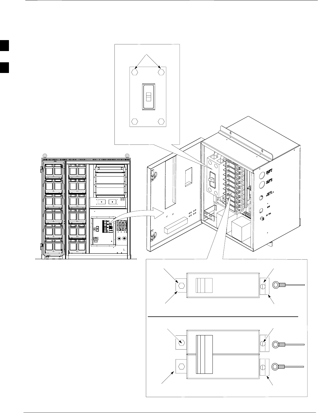
Table 2-2: Initial Inspection and Setup
Step Action
1Verify that ALL AC and DC breakers are turned OFF in both the Power and RF cabinets. Verify that
the DC power cables between the Power and RF cabinets are connected with the correct polarity
2The RED cables connect to the uppermost three (3) terminals (marked +) in both cabinets. Confirm
that the split phase 240/120 AC supply is correctly connected to the AC load center input.
2
Initial Power Up – continued
DRAFT
SCt4812ET BTS Optimization/ATP — CDMA LMF Apr 2001
2-4
Failure to connect the proper AC feed will damage the
surge protection module inside the AC load center.
CAUTION
Power Up Sequence
The first task in the power up sequence is to apply AC power to the
Power cabinet. Once power is applied a series of AC Voltage
measurements is required.
Table 2-3: AC Voltage Measurements
Step Action
1Measure the AC voltages connected to the AC load center (access the terminals from the rear of the
cabinet after removing the AC load center rear panel). See Figure 2-2.
2Measure the AC voltage from terminal L1 to neutral. This voltage should be in the range of nominally
115 to 120 V AC.
3Measure the AC voltage from terminal L1 to ground. This voltage should be in the range of nominally
115 to 120 V AC.
4Measure the AC voltage from terminal L2 to neutral. This voltage should be in the range of nominally
115 to 120 V AC.
5Measure the AC voltage from terminal L2 to ground. This voltage should be in the range of nominally
115 to 120 V AC.
6Measure L1 – L2 – should be from 208 to 240 V AC.
If the AC voltages are in excess of 120 V (or exceed
200 V) when measuring between terminals L1 or L2 to
neutral or ground, STOP and Do Not proceed until the
cause of the higher voltages are determined. The power
cabinet WILL be damaged if the Main breaker is turned
on with excessive voltage on the inputs.
CAUTION
2
Initial Power Up – continued
Apr 2001 2-5
SCt4812ET BTS Optimization/ATP — CDMA LMF
DRAFT
Figure 2-2: AC Load Center Wiring
G= Ground
N = Neutral
L1 = Line 1
L2 = Line 2
G
N
AC to Pilot Beacon
L2
L1
FW00305
Applying AC Power
Once AC Voltage Measurements are complete, apply AC power to the
Power Cabinet. Table 2-4 provides the procedure for applying AC
power.
Table 2-4: Applying AC Power
Step Action
1When the input voltages are verified as correct, turn the Main AC breaker (located on the front of the
AC Load Center) ON. Observe that all eight (8) green LEDs on the front of the AC Load Center are
illuminated (see Figure 2-7).
2Turn Rectifier 1 and Rectifier 2 AC branch breakers (on the AC Load Center) ON. All the installed
rectifier modules (see Figure 2-7) will start up and should each have two green LEDs (DC and Power)
illuminated.
3Turn the Meter Alarm Panel module, ON (see Figure 2-3), while observing the K2 contact in the
PDA assembly (see Figure 2-9). The contact should close. The Meter Alarm Panel voltage meter
should read approximately 27.4 + 0.2 Vdc.
4Turn the Temperature Compensation Panel (TCP) ON, (see Figure 2-4). Verify that the Meter Alarm
Control Panel does not have any alarm LEDs illuminated.
5Check the rectifier current bargraph displays (green LED display on the rectifier module). None
should be illuminated at this point.
If batteries are fitted, turn on the two battery heater AC
breakers on the AC Load Center.
NOTE
2
Initial Power Up – continued
DRAFT
SCt4812ET BTS Optimization/ATP — CDMA LMF Apr 2001
2-6
Figure 2-3: Meter Alarm Panel
OFF
VOLT
VOLT
–
+
TEST POINTS
AMPS
–
+
TEST POINTS
AMP
PWR
ON
FRONT VIEW FW00245
Figure 2-4: Temperature Compensation Panel
OFF
V ADJ
SENSOR 25_ c
SENSE
–
+
COM
ON
ON
FRONT VIEW
1/2 A 250V
12
TEMPERATURE COMPENSATION PANEL
FW00246
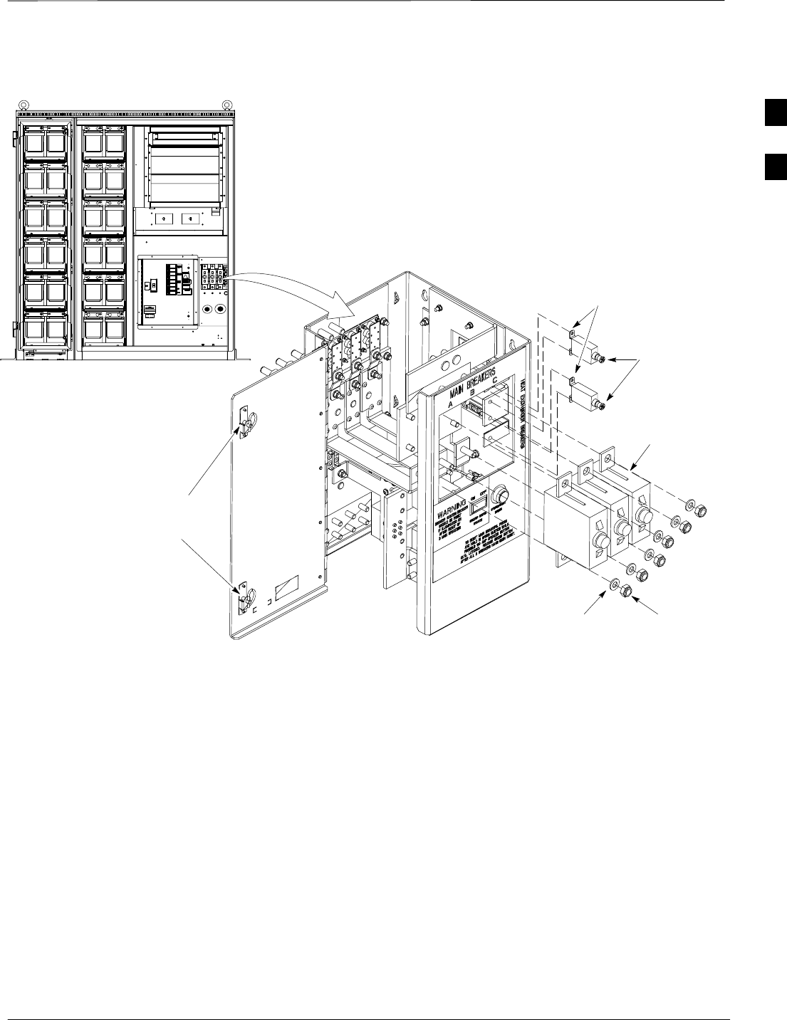
Power Cabinet Power Up
Tests
Table 2-5 lists the step–by–step instructions for Power Up Tests.
Table 2-5: Power Cabinet Power Up Tests
Step Action
1Probe the output voltage test point on the Meter Alarm Panel while pressing the 25° C set button on
the TCP (see Figure 2-4). The voltage should read 27.4 + 0.2 Vdc. Adjust Master Voltage on Meter
Alarm Panel if necessary. Release the TCP 25° C set button.
2Depending on the ambient temperature, the voltage reading may now change by up to + 1.5 V
compared to the reading just measured. If it is cooler than 25_C, the voltage will be higher, and if it is
warmer than 25_C, the voltage will be lower.
3Ensure the RF cabinet 400 Amp main DC breaker is OFF.
4Close the three (3) Main DC breakers on the Power Cabinet ONLY. Close by holding in the reset
button on the front of the PDA, and engaging one breaker at a time.
5Measure the voltage between the + and – terminals at the rear of the Power Cabinet and the RF
Cabinet, observing that the polarity is correct. The voltage should be the same as the measurement in
step 2.
6Place the probes across the black and red battery buss bars in each battery compartment. Place the
probe at the bottom of the buss bars where the cables are connected. The DC voltage should measure
the same as the previous step.
2

Initial Power Up – continued
Apr 2001 2-7
SCt4812ET BTS Optimization/ATP — CDMA LMF
DRAFT
DC Power Pre-test (BTS Frame) Before applying any power to the BTS cabinet, verify there are no shorts
in the RF or power DC distribution system (see Figure 2-5).
Table 2-6: DC Power Pre–test (BTS Frame)
Step Action
1Physically verify that all AC rectifiers supplying power to the RF cabinets are OFF or disabled (see
Figure 2-5). There should be no 27 Vdc on DC feed terminals.
2On each RF cabinet:
SUnseat all circuit boards/ modules in the distribution shelf, transceiver shelf, and Single Carrier
Linear Power Amplifier (SCLPA) shelves, but leave them in their associated slots.
SUnseat all circuit boards (except CCD and CIO cards) in the C–CCP shelf and LPA shelves, but
leave them in their associated slots.
SSet C–CCP shelf breakers to the OFF position by pulling out power distribution breakers (labeled
C–CCP 1, 2, 3 – located on the power distribution panel).
SSet LPA breakers to the OFF position by pulling out power distribution breakers (8 breakers,
labeled 1A–1B through 4C–4D – located on the power distribution panel).
3Verify that the resistance from the power (+) feed terminals with respect to the ground terminal on the
cabinet measures > 500 Ω (see Figure 2-5).
SIf reading is < 500 Ω, a short may exist somewhere in the DC distribution path supplied by the
breaker. Isolate the problem before proceeding. A reading > 3 MΩ could indicate an open (or
missing) bleeder resistor (installed across the filter capacitors behind the breaker panel).
4Set the 400 Amp Main Breaker and the C–CCP breakers (C–CCP 1, 2, 3) to the ON position by
pushing them IN one at a time. Repeat step 3 after turning on each breaker.
* IMPORTANT
If, after inserting any board/module, the ohmmeter stays at 0 Ω, a short probably exists in that
board/module. Replace the suspect board/module and repeat the test. If test still fails, isolate the
problem before proceeding.
5Insert and lock the DC/DC converter modules into their associated slots one at a time. Repeat step3
after inserting each module.
SA typical response is that the ohmmeter will steadily climb in resistance as capacitors charge, finally
indicating approximately 500 Ω.
! CAUTION
Verify the correct power/converter modules by observing the locking/retracting tabs appear as follows:
– (in +27 volt systems)
6Insert and lock all remaining circuit boards and modules into their associated slots in the C–CCP shelf.
Repeat step 3 after inserting and locking each board or module.
SA typical response is that the ohmmeter will steadily climb in resistance as capacitors charge,
stopping at approximately 500 Ω..
. . . continued on next page
2

Initial Power Up – continued
DRAFT
SCt4812ET BTS Optimization/ATP — CDMA LMF Apr 2001
2-8
Table 2-6: DC Power Pre–test (BTS Frame)
Step Action
7Set the 8 LPA breakers ON by pushing them IN one at a time. Repeat step 3 after turning on each
breaker.
SA typical response is that the ohmmeter will steadily climb in resistance as capacitors charge,
stopping at approximately 500 Ω..
8Seat all LPA and associated LPA fan modules into their associated slots in the shelves one at a time.
Repeat step 3 after seating each LPA and associated LPA fan module.
SA typical response is that the ohmmeter will steadily climb in resistance as capacitors charge,
stopping at approximately 500 Ω..
9Seat the Heat Exchanger, ETIB, and Options breakers one at a time. Repeat step 3.
RF Cabinet Power Up
Table 2-7 covers the procedures for properly powering up the RF
Cabinet.
Table 2-7: RF Cabinet Power Up
Step Action
1Ensure the 400 Amp Main DC breaker and all other breakers in the RF Cabinet are OFF.
2Proceed to the DC Power Pre–test (BTS Frame) sequence (see Table 2-6) (for initial power–up as
required).
3Ensure the power cabinet is turned on (see Table 2-5). Verify that 27 volts is applied to the terminals
on the back of the RF cabinet.
4Engage the main DC circuit breaker on the RF cabinet (see Figure 2-5).
5On each RF cabinet:
SSet C–CCP shelf breakers to the ON position by pushing them in one at a time (labeled
C–CCP 1, 2, 3 – located on the power distribution panel).
SSet LPA breakers to the ON position by pushing them in one at a time (8 breakers, labeled 1A–1B
through 4C–4D – located on the power distribution panel).
SSet the two heat exchanger breakers to the ON position by pushing them in one at a time.
SSet the ETIB breaker to the ON position by pushing it in.
SSet the OPTION breaker to the ON position by pushing it in.
. . . continued on next page
2
Initial Power Up – continued
Apr 2001 2-9
SCt4812ET BTS Optimization/ATP — CDMA LMF
DRAFT
Table 2-7: RF Cabinet Power Up
Step Action
6Measure the voltage drop between the Power Cabinet meter test point and the 27 V buss bar inside the
RF Cabinet PDA while the RF Cabinet is transmitting.
NOTE
For a three (3) sector carrier system, the voltage drop should be less than 0.2 V.
For a twelve (12) sector carrier system, the voltage drop should be less than 0.3 V.
7Using a DC current probe, measure the current in each of the six (6) DC cables that are connected
between the RF and Power Cabinet. The DC current measured should be approximately the same. If
there is a wide variation between one cable and the others (>20 A), check the tightness of the
connections (torque settings) at each end of the cable.
RF CABINET
(Rear View)
27V
27V Ret
Figure 2-5: RF Cabinet Circuit Breaker Panel and 27V DC Terminal Locations
MAIN BREAKER 5 RU RACK
SPACE
SC 4812ET BTS RF Cabinet
(Front View)
400
30
30
30
30
30
30
30
30
50
50
50
L
P
A
1B
1D
2B
2D
3B
3D
4B
4D
1A
1C
2A
2C
3A
3C
4A
4C
PS1
PS2
PS3
C
C
C
P
25
25
ETIB
OPTION
10
15
HEAT EXCHANGER
CAUTION
SHUT OFF BOTH BREAKERS
ONLY DURING HEAT EXCHANGER
MAINTENANCE OR REPAIR
LPA
BLOWERS
PUSH BUTTON
TO RESET
LPA BLOWERS
FW00307
I/O Plate + and – DC Feed
Terminals (Back Panel of RF
Cabinet)
2

Initial Power Up – continued
DRAFT
SCt4812ET BTS Optimization/ATP — CDMA LMF Apr 2001
2-10
Battery Charge Test
(Connected Batteries)
Table 2-8 lists the step–by–step instructions for testing the batteries.
Table 2-8: Battery Charge Test (Connected Batteries)
Step Action
1Close the battery compartment breakers for connected batteries ONLY. This process should be
completed quickly to avoid individual battery strings with excess charge current
NOTE
If the batteries are sufficiently discharged, the battery circuit breakers may not engage individually
due to the surge current. If this condition is observed, turn off the Meter Alarm Panel power switch,
and then engage all the connected battery circuit breakers, the Meter Alarm Panel power switch
should then be turned ON.
2Using the DC current probe, measure the current in each of the battery string connections to the buss
bars in each battery cabinet. The charge current may initially be high but should quickly reduce in a
few minutes if the batteries have a typical new battery charge level.
3The current in each string should be approximately equal (+ 5 A).
4The bargraph meters on the rectifier modules can be used as a rough estimate of the total battery
charge current. Each rectifier module has eight (8) LEDs to represent the output current. Each
illuminated LED indicates that approximately 12.5% (1/8 or 8.75 A) of the rectifiers maximum (70 A)
current is flowing.
EXAMPLE:
Question: A system fitted with three (3) rectifier modules each have three bargraph LEDs
illuminated. What is the total output current into the batteries?
Answer: Each bargraph is approximately indicating 12.5% of 70 A, therefore, 3 X 8.75 equals
26.25 A. As there are three rectifiers, the total charge current is equal to (3 X 26.25 A) 78.75 A.
This charge current calculation only applies at this part of the start up procedure, when the RF Cabinet
is not powered on, and the power cabinet heat exchanger is turned off.
5Allow a few minutes to ensure that the battery charge current stabilizes before taking any further
action. Recheck the battery current in each string. If the batteries had a reasonable charge, the current
in each string should reduce to less than 5 A.
6Recheck the DC output voltage. It should remain the same as measured in step 4 of the Power Up
Test.
NOTE
If discharged batteries are installed, all bargraphs may be illuminated on the rectifiers during the
charge test. This indicates that the rectifiers are at full capacity and are rapidly charging the batteries.
It is recommended in this case that the batteries are allowed to charge and stabilize as in the above
step before commissioning the site. This could take several hours.
Battery Discharge Test
Perform the test procedure in Table 2-9 only when the battery current is
less than 5 A per string. Refer to Table 2-8 on the procedures for
checking current levels.
2
Initial Power Up – continued
Apr 2001 2-11
SCt4812ET BTS Optimization/ATP — CDMA LMF
DRAFT
Table 2-9: Battery Discharge Test
Step Action
1Turn the battery test switch on the Meter Alarm Panel, ON (see Figure 2-3). The rectifier output
voltage and current should decrease by approximately 10% as the batteries assume the load. Alarms
for the Meter Alarm Panel may occur.
2Measure the individual battery string current using the DC current probe. The battery discharge
current in each string should be approximately the same (within + 5 A).
3Turn Battery Test Switch OFF.
Failure to turn OFF the Battery Test Switch before leaving
the site, will result in low battery capacity and reduce
battery life.
CAUTION
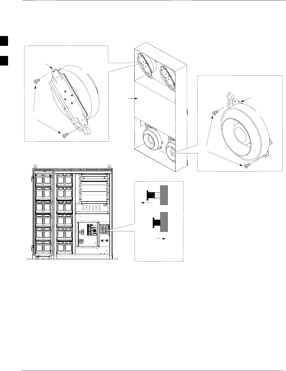
Heat Exchanger Power Up
Table 2-10: Heat Exchanger Power Up
Step Action
1Turn the Power Cabinet Heat Exchanger breakers ON (seeFigure 2-6 for breaker location).
2The Heat Exchanger will now go into a 5 minute test sequence. Ensure that the internal and external
fans are operating. Place a hand on the internal and external Heat Exchanger grills to feel for air draft.
2
Initial Power Up – continued
DRAFT
SCt4812ET BTS Optimization/ATP — CDMA LMF Apr 2001
2-12
Core
Heat Exchanger
Assembly
POWER CABINET
Front View
OUT=OFF
IN=ON
Blower Assembly
Circuit Breaker
FW00181
Side View
Mounting
Bracket
T–30 Screw
Top (Internal) Blower
Fan Module
Blower
Power
Cord
Blower
Power
Cord
Bottom (Ambient) Blower
Fan Module
T–30 Screw
Mounting
Bracket
Figure 2-6: Heat Exchanger Blower Assembly
2
Initial Power Up – continued
Apr 2001 2-13
SCt4812ET BTS Optimization/ATP — CDMA LMF
DRAFT
LED Status
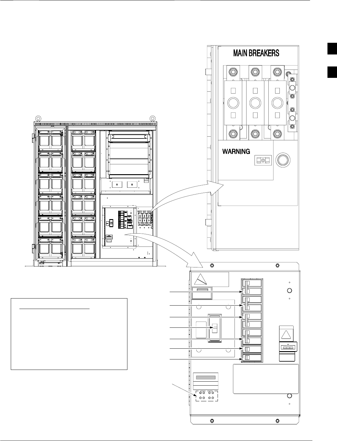
Figure 2-7: Power Cabinet Circuit Breaker Assemblies
A B C
BREAKER SYSTEM BREAKER
SHOULD BE RESET
IF ILLUMINATED OR
AFTER RESET OF
3 MAIN BREAKERS
TO RESET MAIN BREAKERS, PRESS
AND HOLD IN GREEN BUTTON WHILE
PRESSING 160 AMP BREAKER BUTTON
UNTIL LATCHED RELEASE GREEN BUTTON
AFTER ALL 3 BREAKERS HAVE BEEN RESET
ON OFF
BREAKER SYSTEM
BREAKER
SYSTEM RESET
BUTTON
FW00144
POWER CABINET
Front View
AC Circuit
Breaker
DC Circuit
Breaker
160 160 160
25
25
Circuit Breaker Legend:
1. Main 150 Amp. . . . . . . . . . . . . . .
2. Rectifier Shelf #1 70 Amp. . . .
3. Rectifier Shelf #2 70 Amp. . . .
4. Battery Heater #1 15 Amp. . . .
5. Battery Heater #2 15 Amp. . . .
6. GFCI 15 Amp. . . . . . . . . . . . . . .
7. Spare 15 Amp. . . . . . . . . . . . . .
RECTIFIER
SHELF #1
RECTIFIER
SHELF #2
BATTERY
HEATER #1
GFCI
SPARE
BATTERY
HEATER #2
CAUTION
LIVE TERMINALS
2
3
4
5
6
1
7
ATTENTION
MAIN
2
Initial Power Up – continued
DRAFT
SCt4812ET BTS Optimization/ATP — CDMA LMF Apr 2001
2-14
15 Amp Breaker
5/16 NUT
LEFT TAB
SCREW
WIRE
RIGHT TAB
30 Thru 140 Amp Breaker
Figure 2-8: Power Cabinet AC Circuit Breakers
150 Amp Breaker
7/16 NUT
POWER CABINET
Front View
AC Circuit Breaker
FW00145
SCREW
WIRE
RIGHT
TABS
WIRE
5/16 NUT
LEFT TABS
2
Initial Power Up – continued
Apr 2001 2-15
SCt4812ET BTS Optimization/ATP — CDMA LMF
DRAFT
Figure 2-9: Power Cabinet DC Circuit Breakers
POWER CABINET
Front View
DC Circuit Breaker
FW00146
15 AMP
3x150 AMP
Flat Washer
Lock Washer 17 mm Nut
DC Power
Panel Door
Locks
9/32 Nut
2

Initial Power Up – continued
DRAFT
SCt4812ET BTS Optimization/ATP — CDMA LMF Apr 2001
2-16
Notes
2
Optimization/Calibration – Introduction
Apr 2001 3-1
SCt4812ET BTS Optimization/ATP — CDMA LMF
DRAFT
Introduction
This chapter provides procedures for downloading system operating
software, set up of the supported test equipment, CSM reference
verification/optimization, and transmit/receive path verification.
Before using the LMF, use an editor to view the
”CAVEATS” section in the ”readme.txt” file in the c:\wlmf
folder for any applicable information.
IMPORTANT
*
Optimization Process
After a BTS is physically installed and the preliminary operations
(power up) have been completed, the CDMA LMF is used to calibrate
and optimize the BTS. The basic optimization process can be
accomplished as follows:
SDownload MGLI2–1 with code and data and then enable MGLI2–1.
SUse the status function and verify that all of the installed devices of
the following types respond with status information: CSM2, BBX2,
GLI2, and MCC (and TSU if RFDS is installed). If a device is
installed and powered up but is not responding and is colored gray in
the BTS display, the device is not listed in the CDF file. The CDF file
will have to be corrected before the device can be accessed by CDMA
LMF.
SDownload code and data to all devices of the following types:
– CSM2
– BBX
–GLI2 (other than MGLI2–1)
– MCC
SDownload the RFDS TSIC (if installed).
SVerify the operation of the GPS and HSO signals.
SEnable the following devices (in the order listed):
–Secondary CSM (slot 2)
–Primary CSM (slot 1)
–All MCCs
SConnect the required test equipment for a full optimization.
SSelect the test equipment.
SCalibrate the TX and RX test cables if they have not previously been
calibrated using the CDMA LMF that is going to be used for the
optimization/calibration. The cable calibration values can also be
entered manually.
. . . continued on next page
3

Optimization/Calibration – Introduction – continued
DRAFT
SCt4812ET BTS Optimization/ATP — CDMA LMF Apr 2001
3-2
SSelect all of the BBXs and all of the MCCs and use the full
optimization function. The full optimization function performs TX
calibration, BLO download, TX audit, all TX tests, and all RX tests
for all selected devices.
SIf the TX calibration fails, repeat the full optimization for any failed
paths.
SIf the TX calibration fails again, correct the problem that caused the
failure and repeat the full optimization for the failed path.
SIf the TX calibration and audit portion of the full optimization passes
for a path but some of the TX or RX tests fail, correct the problem that
caused the failure and run the individual tests as required until all TX
and RX tests have passed for all paths.
Cell–site Types
Sites are configured as Omni/Omni or Sector/Sector (TX/RX). Each type
has unique characteristics and must be optimized accordingly.
Cell–site Data File
The CDF includes the following information:
SDownload instructions and protocol
SSite specific equipage information
SC–CCP shelf allocation plan
–BBX2 equipage (based on cell–site type) including redundancy
–CSM equipage including redundancy
–MCC (MCC24E, MCC8E or MCC–1X) channel element allocation
plan. This plan indicates how the C–CCP shelf is configured, and
how the paging, synchronization, traffic, and access channel
elements (and associated gain values) are assigned among the (up to
12) MCCs in the shelf.
SCSM equipage including redundancy
SEffective Rated Power (ERP) table for all TX channels to antennas
respectively. Motorola System Engineering specifies the ERP of a
transmit antenna based on site geography, antenna placement, and
government regulations. Working from this ERP requirement, the
antenna gain, (dependent on the units of measurement specified) and
antenna feed line loss can be combined to determine the required
power at the top of the BTS frame. The corresponding BBX2 output
level required to achieve that power level on any channel/sector can
also be determined.
Refer to the CDMA LMF Operator’s Guide, 68P64114A78,
for additional information on the layout of the LMF
directory structure (including CDF file locations and
formats).
NOTE
3
Optimization/Calibration – Introduction – continued
Apr 2001 3-3
SCt4812ET BTS Optimization/ATP — CDMA LMF
DRAFT
BTS System Software
Download
BTS system software must be successfully downloaded to the BTS
processor boards before optimization can be performed. BTS operating
code is loaded from the LMF computer terminal.
Before using the LMF for optimization/ATP, the correct
bts–#.cdf and cbsc–#.cdf files for the BTS must be
obtained from the CBSC and put in a bts–# folder in the
LMF. Failure to use the correct CDF files can cause wrong
results. Failure to use the correct CDF files to log into a
live (traffic carrying) site can shut down the site.
IMPORTANT
*
The CDF is normally obtained from the CBSC on a DOS formatted
diskette, or through a file transfer protocol (ftp) if the LMF computer has
ftp capability. Refer to the CDMA LMF Operator’s Guide,
68P64114A78, or the LMF Help screen, for more information.
Site Equipage Verification
If you have not already done so, use an editor to view the CDF, and
review the site documentation. Verify the site engineering equipage data
in the CDF to the actual site hardware.
Always wear a conductive, high impedance wrist strap
while handling any circuit card/module to prevent damage
by ESD. Extreme care should be taken during the removal
and installation of any card/module. After removal, the
card/module should be placed on a conductive surface or
back into the anti–static bag in which it was shipped.
CAUTION
3

Isolate Span Lines/Connect LMF
DRAFT
SCt4812ET BTS Optimization/ATP — CDMA LMF Apr 2001
3-4
Isolate BTS from T1/E1 Spans
–At active sites, the OMC/CBSC must disable the
BTS and place it out of service (OOS). DO NOT
remove the span surge protectors until the
OMC/CBSC has disabled the BTS.
IMPORTANT
*
Each frame is equipped with one 50–pair punch block for spans,
customer alarms, remote GPS, and power cabinet alarms. See Figure 3-2
and refer to Table 3-1 for the physical location and pin call–out
information. To disable the span, pull the surge protectors for the
respective span.
Before connecting the LMF to the frame LAN, the OMC/CBSC must
disable the BTS and place it OOS to allow the LMF to control the
CDMA BTS. This prevents the CBSC from inadvertently sending
control information to the CDMA BTS during LMF based tests.
Configure Channel Service
Unit
The M–PATH 537 Channel Service Unit (CSU) provides in–band
SNMP–managed digital service access to T1 and fractional T1 lines.
M–PATH units plug into the ADC Kentrox 2–slot frame (see
Figure 3-1).
Remote M–PATH management is available via SNMP over an in–band
data link on the T1 line (using a facility data link or 8–64 Kbps of a DS0
channel). The unit at the near end of the management path can be an
SNMP manager or another M–PATH CSU.
Each 19 inch rack can support two CSU M–PATH 537 modules. Each
M–PATH 537 module supports one and only one span connection.
Programming of the M–PATH is accomplished through the DCE 9–pin
connector on the front panel of the CSU shelf. Manuals and a Microsoft
Windows programming disk is supplied with each unit.
3
Isolate Span Lines/Connect LMF – continued
Apr 2001 3-5
SCt4812ET BTS Optimization/ATP — CDMA LMF
DRAFT
Setting the Control Port
Whichever control port is chosen, it must first be set up so the control
port switches match the communication parameters being used by the
control device. If using the rear–panel DTE control port, set the
shelf–address switch SA5 to “up” (leave the switch down for the
rear–panel DCE control port).
For more information, refer to the Kentrox Installation Guide, manual
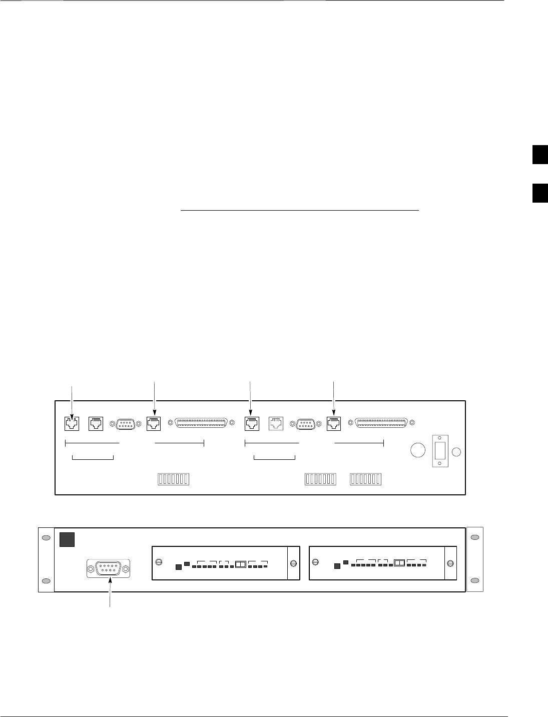
number 65–77538001 which is provided with each CSU.
Plug one of the cables listed below into the Control Port connectors:
Part Number Description of Cable
01–95006–022 (six feet) DB–9S to DB–9P
01–95010–022 (ten feet)
The control port cables can be used to connect the shelf to:
SA PC using the AT 9–pin interface
SA modem using the 9–pin connector
SOther shelves in a daisy chain
Figure 3-1: Back and Front View of the CSU
REF. FW00212
Front View
SLOT 1 SLOT 2
DCE Connector
(Craft Port)
SLOT 1SLOT 2 T1 TERMINAL T1 TERMINAL
CONTROL
PORT GROUP
ADDRESS SHELF
ADDRESS
T1 DDS T1 DDS
DTE DCEDATA PORT DATA PORT
Back View
NETWORK NETWORK
To/From
Network To/From
GLI
To/From
Network To/From
GLI
3
Isolate Span Lines/Connect LMF – continued
DRAFT
SCt4812ET BTS Optimization/ATP — CDMA LMF Apr 2001
3-6
Alarm and Span Line Cable
Pin/Signal Information
See Figure 3-2 and refer to Table 3-1 for the physical location and pin
call–out information for the 50–pin punch block.
Figure 3-2: 50 Pair Punch Block
TOP VIEW OF PUNCH BLOCK
STRAIN RELIEVE INCOMING
CABLE TO BRACKET WITH
TIE WRAPS
2T
1T 1R 2T 2R
12
1R
2R
LEGEND
1T = PAIR 1 – TIP
1R = PAIR 1 –RING
” ”
” ”
” ”
RF Cabinet I/O Area
50R
50T
49R
49T
1T
FW00162
TO LAN
CONNECTOR
TO ALARMS
CONNECTOR
TO MODEM
CONNECTOR
TO RGD/RGPS
CONNECTOR
3

Isolate Span Lines/Connect LMF – continued
Apr 2001 3-7
SCt4812ET BTS Optimization/ATP — CDMA LMF
DRAFT
Table 3-1: Pin–Out for 50 Pin Punch Block
Site Component Signal Name Pin Color
Power Cab Control – NC 1T Blue
Power Cab Control – NO 1R Blk/Blue
Power Cab Control – Com 2T Yellow
Reserved 2R N/C
Rectifier Fail 3T Blk/Yellow
AC Fail 3R Green
POWER CABINET Power Cab Exchanger Fail 4T Blk/Grn
POWER CABINET Power Cab Door Alarm 4R White
Power Cab Major Alarm 5T Blk/Whit
Battery Over Temp 5R Red
Power Cab Minor Alarm 6T Blk/Red
Reticifier Over Temp 6R Brown
Power Cab Alarm Rtn 7T Blk/Brn
LFR_HSO_GND 7R
EXT_1PPS_POS 8T
EXT_1PPS_NEG 8R
LFR / HSO CAL_+ 9T
LFR / HSO CAB_– 9R
LORAN_+ 10T
LORAN_– 10R
Pilot Beacon Alarm – Minor 11T
Pilot Beacon Alarm – Rtn 11R
Pilot Beacon Alarm – Major 12T
PILOT BEACON Pilot Beacon Control – NO 12R
Pilot Beacon Control–COM 13T
Pilot Beacon Control – NC 13R
Customer Outputs 1 – NO 14T
Customer Outputs 1 – COM 14R
Customer Outputs 1 – NC 15T
Customer Outputs 2 – NO 15R
Customer Outputs 2 – COM 16T
Customer Outputs 2 – NC 16R
Customer Outputs 3 – NO 17T
Customer Outputs 3 – COM 17R
Customer Outputs 3 – NC 18T
Customer Outputs 4 – NO 18R
Customer Outputs 4–COM 19T
Customer Outputs 4 – NC 19R
Customer Inputs 1 20T
Cust_Rtn_A_1 20R
Customer Inputs 2 21T
CUSTOMER Cust_Rtn_A_2 21R
CUSTOMER
OUTPUTS / INPUTS Customer Inputs 3 22T
Cust_Rtn_A_3 22R
Customer Inputs 4 23T
Cust_Rtn_A_4 23R
Customer Inputs 5 24T
Cust_Rtn_A_5 24R
Customer Inputs 6 25T
Cust_Rtn_A_6 25R
Customer Inputs 7 26T
Cust_Rtn_A_7 26R
Customer Inputs 8 27T
Cust_Rtn_A_8 27R
Customer Inputs 9 28T
Cust_Rtn_A_9 28R
Customer Inputs 10 29T
Cust_Rtn_A_10 29R
. . . continued on next page
3

Isolate Span Lines/Connect LMF – continued
DRAFT
SCt4812ET BTS Optimization/ATP — CDMA LMF Apr 2001
3-8
Table 3-1: Pin–Out for 50 Pin Punch Block
Site Component ColorPinSignal Name
RVC_TIP_A 30T
RVC_RING_A 30R
XMIT_TIP_A 31T
XMIT_RING_A 31R
RVC_TIP_B 32T
RVC_RING_B 32R
XMIT_TIP_B 33T
XMIT_RING_B 33R
RVC_TIP_C 34T
RVC_RING_C 34R
XMIT_TIP_C 35T
XMIT_RING_C 35R
SPAN RVC_TIP_D 36T
RVC_RING_D 36R
XMIT_TIP_D 37T
XMIT_RING_D 37R
RVC_TIP_E 38T
RVC_RING_E 38R
XMIT_TIP_E 39T
XMIT_RING_E 39R
RVC_TIP_F 40T
RVC_RING_F 40R
XMIT_TIP_F 41T
XMIT_RING_F 41R
GPS_POWER_1+ 42T Blue
GPS_POWER_1– 42R Bk/Blue
GPS_POWER_2+ 43T Yellow
GPS_POWER_2– 43R Bk/Yellow
GPS_RX+ 44T White
GPS_RX– 44R White
RGPS GPS_TX+ 45T Green
GPS_TX– 45R Green
Signal Ground (TDR+) 46T Red
Master Frame (TDR–) 46R Bk/Red
GPS_lpps+ 47T Brown
GPS_lpps– 47R Bk/Brn
Telco_Modem_T 48T
Phone Line Telco_Modem_R 48R
Chasis Ground 49T
Reserved 49R
Miscellaneous Reserved 50T
Reserved 50R
3

Isolate Span Lines/Connect LMF – continued
Apr 2001 3-9
SCt4812ET BTS Optimization/ATP — CDMA LMF
DRAFT
T1/E1 Span Isolation
Table 3-2 describes the action required for span isolation.
Table 3-2: T1/E1 Span Isolation
Step Action
1The OMC/CBSC must disable the BTS and place it OOS.
The Span Lines can be disabled by removing the surge protectors on the 50–pin punch block. Using
Table 3-1 locate the span or spans which need to be disabled and remove the respective surge
protector.
NOTE
If a third party is used for span connectivity, the third party must be informed before disabling the span
line.
3

Preparing the LMF
DRAFT
SCt4812ET BTS Optimization/ATP — CDMA LMF Apr 2001
3-10
Software and files for installation and updating of the LMF are provided
on CD ROM disks. The following installation items must be available:
SLMF Program on CD ROM
SLMF Binaries on CD ROM
SCDF for each supported BTS (on diskette or available from the
CBSC)
SCBSC File for each supported BTS (on diskette or available from the
CBSC)
The following section provides information and instructions for
installing and updating the LMF software and files.
LMF Operating System Installation
Follow the procedure in Table 3-3 to install the LMF operating system.
Table 3-3: LMF Operating System Installation
Step Action
1Insert the LMF Program CD ROM into the LMF CD ROM drive.
–If the Setup screen is displayed, go to step 5.
–If the Setup screen is not displayed, proceed to step 2.
2Click on the Start button.
3 Select Run.
4In the Open box, enter d:\autorun and click on the OK button.
NOTE
If applicable, replace the letter d with the correct CD ROM drive letter.
. . . continued on next page
3

Preparing the LMF – continued
DRAFT
Apr 2001 3-11
SCt4812ET BTS Optimization/ATP — CDMA LMF
Table 3-3: LMF Operating System Installation
Step Action
5Follow the instructions displayed on the Setup screen.
* IMPORTANT
First Time Installations:
–Install U/WIN (First)
–Install Java Runtime Environment (Second)
–Install LMF Software (Third)
–Install BTS Binaries (Fourth)
–Install/Create BTS Folders (Fifth)
Any time you install U/WIN, you must install the LMF software because the installation of the LMF
modifies some of the files that are installed during the U/Win installation. Installing U/Win
over–writes these modifications.
NOTE
There are multiple binary image packages for installation on the CD–ROM. When prompted, choose
the load that corresponds to the switch release that you currently have installed. Perform the Device
Images install after the WinLMF installation.
If applicable, a separate CD ROM of BTS Binaries may be available for binary updates.
CDMA LMF Home Directory
The CDMA LMF installation program creates the default home directory
c:\wlmf, and installs the application files and subdirectories (folders)
in it. Because this can be changed at installation, the CDMA LMF home
directory will be referred to with the generic convention of:
<x>:\<lmf home directory>
Where:
<x> = the LMF computer drive letter where the CDMA LMF home
directory is located.
<lmf home directory> = the directory path or name where the CDMA
LMF is installed
The CDMA LMF installation program creates the default
home directory c:\wlmf when the CDMA LMF is
installed.
NOTE
3
Preparing the LMF – continued
DRAFT
SCt4812ET BTS Optimization/ATP — CDMA LMF Apr 2001
3-12
Copy CBSC CDF Files to the
LMF Computer
Before logging on to a BTS with the LMF to execute optimization/ATP
procedures, the correct bts-#.cdf and cbsc–#.cdf files must be obtained
from the CBSC and put in a bts-# folder in the LMF computer. This
requires creating versions of the CBSC CDF files on a DOS–formatted
floppy diskette and using the diskette to install the CDF files on the
LMF computer.
*When copying CDF files, comply with the following to
prevent BTS login problems with the LMF.
– The numbers used in the bts–#.cdf and cbsc–#.cdf
filenames must correspond to the locally assigned numbers
for each BTS and its controlling CBSC.
– The generic cbsc–1.cdf file supplied with the LMF will
work with locally numbered BTS CDF files. Using this file
will not provide a valid optimization unless the generic file
is edited to replace default parameters (e.g., channel
numbers) with the operational parameters used locally.
IMPORTANT
The procedure in Table 3-4 lists the steps required to transfer the CDF
files from the CBSC to the LMF computer. For any further information,
refer to the CDMA LMF Operator’s Guide (Motorola part number
68P64114A21) or the LMF Help screen..
Table 3-4: Copying CBSC CDF Files to the LMF
Step Action
1Login to the CBSC workstation.
2Insert a DOS–formatted floppy diskette in the workstation drive.
3 Type eject –q and press <Enter>.
4 Type mount and press <Enter>.
NOTE
SLook for the “floppy/no_name” message on the last line displayed.
SIf the eject command was previously entered, floppy/no_name will be appended with a number. Use
the explicit floppy/no_name reference displayed when performing step 7.
5Change to the directory, where the files to be copied reside, by typing cd <directoryname>
(e.g., cd bts–248) and pressing <Enter>.
6 Type ls and press the Enter key to display the list of files in the directory.
. . . continued on next page
3

Preparing the LMF – continued
DRAFT
Apr 2001 3-13
SCt4812ET BTS Optimization/ATP — CDMA LMF
Table 3-4: Copying CBSC CDF Files to the LMF
Step Action
7 With Solaris versions of Unix, create DOS–formatted versions of the bts–#.cdf and cbsc–#.cdf files
on the diskette by entering the following command:
unix2dos <source filename> /floppy/no_name/<target filename>
(e.g., unix2dos bts–248.cdf /floppy/no_name/bts–248.cdf).
NOTE
SOther versions of Unix do not support the unix2dos and dos2unix commands. In these cases, use the
Unix cp (copy) command. The copied files will be difficult to read with a DOS or Windows text
editor because Unix files do not contain line feed characters. Editing copied CDF files on the LMF
computer is, therefore, not recommended.
SUsing cp, multiple files can be copied in one operation by separating each filename to be copied
with a space and ensuring the destination directory (floppy/no_name) is listed at the end of the
command string following a space (e.g., cp bts–248.cdf cbsc–6.cdf /floppy/na_name)
8Repeat steps 5 through 7 for each bts–# that must be supported by the LMF.
9When all required files have been copied to the diskette, type eject and press <Enter>.
10 Remove the diskette from the CBSC drive.
11 If it is not running, start the Windows operating system on the LMF computer.
12 Insert the diskette containing the bts–#.cdf and cbsc–#.cdf files into the LMF computer.
13 Using Windows Explorer (or equivalent program), create a corresponding bts–# folder in the <lmf
home directory> directory for each bts–#.cdf/cbsc–#.cdf file pair copied from the CBSC.
14 Use Windows Explorer (or equivalent program) to transfer the cbsc–#.cdf and bts–#.cdf files from the
diskette to the corresponding <lmf home directory>\wlmf\cdma\bts–# folders created in step 13.
Creating a Named
HyperTerminal Connection for
MMI Connection
Confirming or changing the configuration data of certain BTS FRUs
requires establishing an MMI communication session between the LMF
and the FRU. Using features of the Windows operating system, the
connection properties for an MMI session can be saved on the LMF
computer as a named Windows HyperTerminal connection. This
eliminates the need for setting up connection parameters each time an
MMI session is required to support optimization.
Once the named connection is saved, a shortcut for it can be created on
the Windows desktop. Double clicking the shortcut icon will start the
connection without the need to negotiate multiple menu levels.
Follow the procedures in Table 3-5 to establish a named HyperTerminal
connection and create a Windows desktop shortcut for it.
3

Preparing the LMF – continued
DRAFT
SCt4812ET BTS Optimization/ATP — CDMA LMF Apr 2001
3-14
There are differences between Windows NT and Windows
98 in the menus and screens for creating a HyperTerminal
connection. In the following procedure, items applicable
to:
– Windows NT will be identified with Win NT
– Windows 98 will be identified with Win 98
NOTE
Table 3-5: Creating a Named Hyperlink Connection for MMI Connection
Step Action
1From the Windows Start menu, select:
Programs>Accessories
2Perform one of the following:
SFor Win NT, select Hyperterminal and then click on HyperTerminal or
SFor Win 98, select Communications, double click the Hyperterminal folder, and then double click
on the Hyperterm.exe icon in the window that opens.
NOTE
SIf a Location Information Window appears, enter the required information, then click Close.
(This is required the first time, even if a modem is not to be used.)
SIf a You need to install a modem..... message appears, click NO.
3When the Connection Description box opens:
–Type a name for the connection being defined (e.g., MMI Session) in the Name: window.
–Highlight any icon preferred for the named connection in the Icon: chooser window, and
– Click OK.
4
NOTE
For LMF configurations where COM1 is used by another interface such as test equipment and a
physical port is available for COM2, select COM2 to prevent conflicts.
From the Connect using: pick list in the Connect To box displayed, select the RS–232 port to be used
for the connection (e.g., COM1 or COM2 – Win NT – or Direct to Com 1 or Direct to Com 2 – Win
98), and click OK.
5In the Port Settings tab of the COM# Properties window displayed, configure the RS–232 port
settings as follows:
SBits per second: 9600
SData bits: 8
SParity: None
SStop bits: 1
SFlow control: None
. . . continued on next page
3

Preparing the LMF – continued
DRAFT
Apr 2001 3-15
SCt4812ET BTS Optimization/ATP — CDMA LMF
Table 3-5: Creating a Named Hyperlink Connection for MMI Connection
Step Action
6 Click OK.
7Save the defined connection by selecting:
File>Save
8Close the HyperTerminal window by selecting:
File>Exit
9 Click Yes to disconnect when prompted.
10 Perform one of the following:
SIf the Hyperterminal folder window is still open (Win 98) proceed to step 12 or
SFrom the Windows Start menu, select Programs > Accessories
11 Perform one of the following:
SFor Win NT, select Hyperterminal and release any pressed mouse buttons.
SFor Win 98, select Communications and double click the Hyperterminal folder.
12 Highlight the newly created connection icon by moving the cursor over it (Win NT) or clicking on it
(Win 98).
13 Right click and drag the highlighted connection icon to the Windows desktop and release the right
mouse button.
14 From the popup menu displayed, select Create Shortcut(s) Here.
15 If desired, reposition the shortcut icon for the new connection by dragging it to another location on the
Windows desktop.
3

Preparing the LMF – continued
DRAFT
SCt4812ET BTS Optimization/ATP — CDMA LMF Apr 2001
3-16
Folder Structure Overview
The LMF uses an <lmf home directory> folder that contains all of the
essential data for installing and maintaining the BTS. The list that
follows outlines the folder structure for the LMF. Except for the bts–nnn
folders, these folders are created as part of the the LMF installation.
Figure 3-3: LMF Folder Structure
version folder (A separate folder is
required for each different version; for
example, a folder name 2.8.1.1.1.5)
loads folder
<x>:\ (drive letter)
<lmf home directory> folder
cdma folder
code folder
data folder
BTS–nnn folders (A separate folder is
required for each BTS where bts–nnn is the
unique BTS number; for example, bts–163)
3

Preparing the LMF – continued
DRAFT
Apr 2001 3-17
SCt4812ET BTS Optimization/ATP — CDMA LMF
LMF to BTS Connection
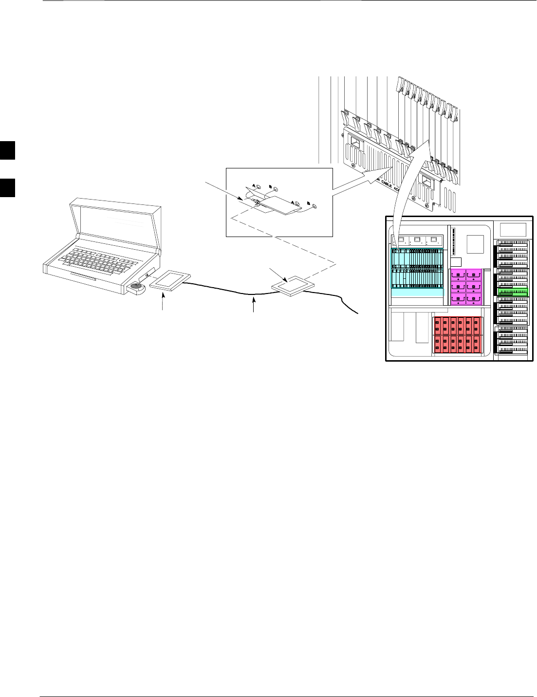
The LMF is connected to the LAN A or B connector located on the left
side of the frame’s lower air intake grill, behind the LAN Cable Access
door (see Figure 3-4).
Table 3-6: LMF to BTS Connection
Step Action
1To gain access to the connectors, open the LAN Cable Access door, then pull apart the Velcro tape
covering the BNC “T” connector and slide out the computer service tray, if desired (see Figure 3-4).
2Connect the LMF to the LAN A BNC connector via PCMCIA Ethernet Adapter with an unshielded
twisted–pair (UTP) Adapter and 10BaseT/10Base2 converter (powered by an external AC/DC
transformer). If there is no login response, connect the LMF to the LAN B BNC connector. If there is
still no login response, see Table 6-1, Login Failure Troubleshooting Procedure.
NOTE
–Xircom Model PE3–10B2 or equivalent can also be used to interface the LMF Ethernet
connection to the frame connected to the PC parallel port, powered by an external AC/DC
transformer. In this case, the BNC cable must not exceed 91 cm (3 ft) in length.
* IMPORTANT
The LAN shield is isolated from chassis ground. The LAN shield (exposed portion of BNC connector)
must not touch the chassis during optimization.
3
Preparing the LMF – continued
DRAFT
SCt4812ET BTS Optimization/ATP — CDMA LMF Apr 2001
3-18
RFDS
EBA
ETIB
LMF BNC “T” CONNECTIONS
ON LEFT SIDE OF FRAME
(ETHERNET “A” SHOWN;
ETHERNET “B” COVERED
WITH VELCRO TAPE)
LMF COMPUTER
TERMINAL WITH
MOUSE PCMCIA ETHERNET
ADPATER & ETHERNET
UTP ADAPTER
UNIVERSAL TWISTED
PAIR (UTP) CABLE (RJ11
CONNECTORS)
10BASET/10BASE2
CONVERTER CONNECTS
DIRECTLY TO BNC T
115 VAC POWER
CONNECTION
FW00168
SC4812ET RF CABINET
NOTE:
Open LAN CABLE ACCESS
door. Pull apart Velcro tape and
gain access to the LAN A or LAN
B LMF BNC connector.
Figure 3-4: LMF Connection Detail
3
Preparing the LMF – continued
DRAFT
Apr 2001 3-19
SCt4812ET BTS Optimization/ATP — CDMA LMF
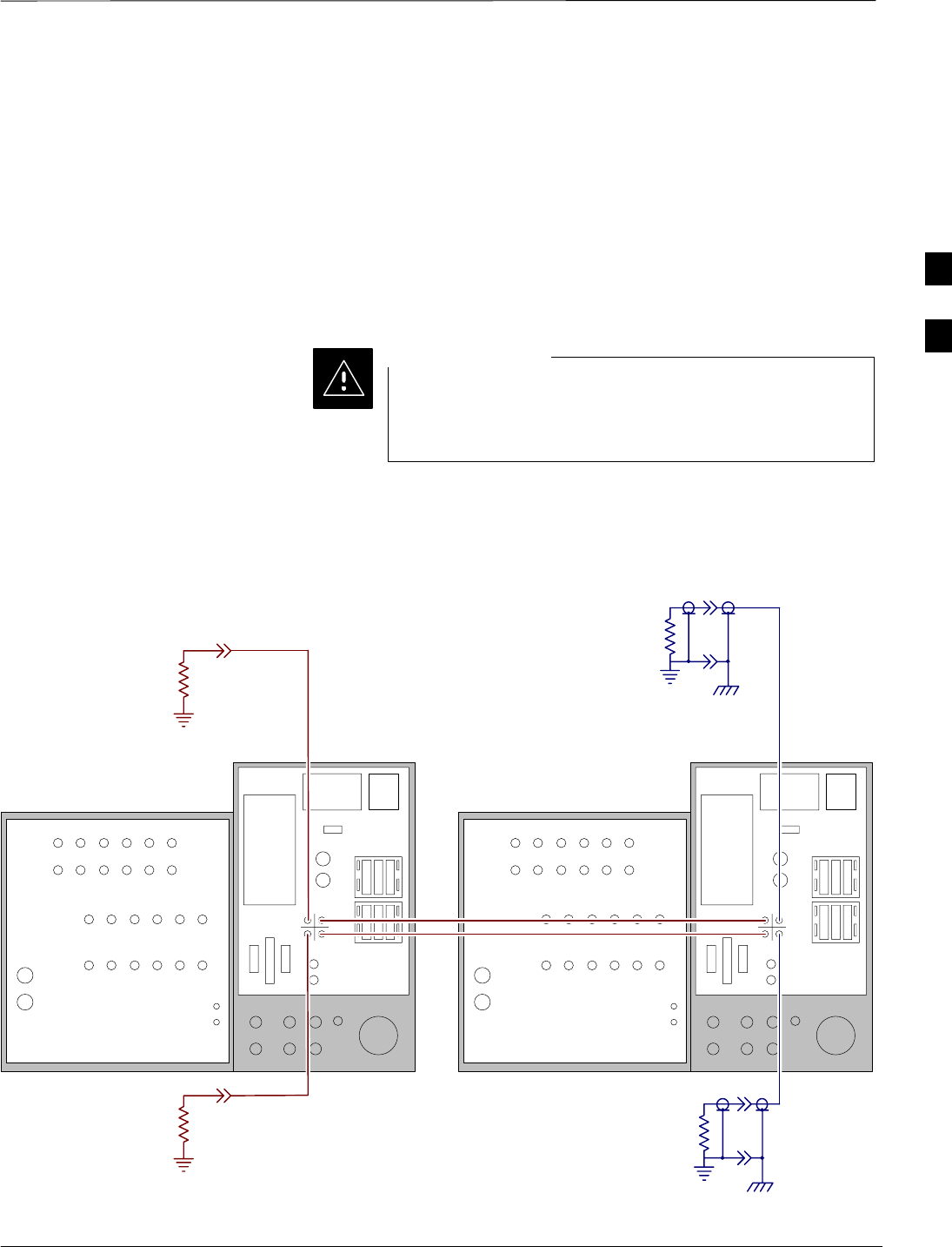
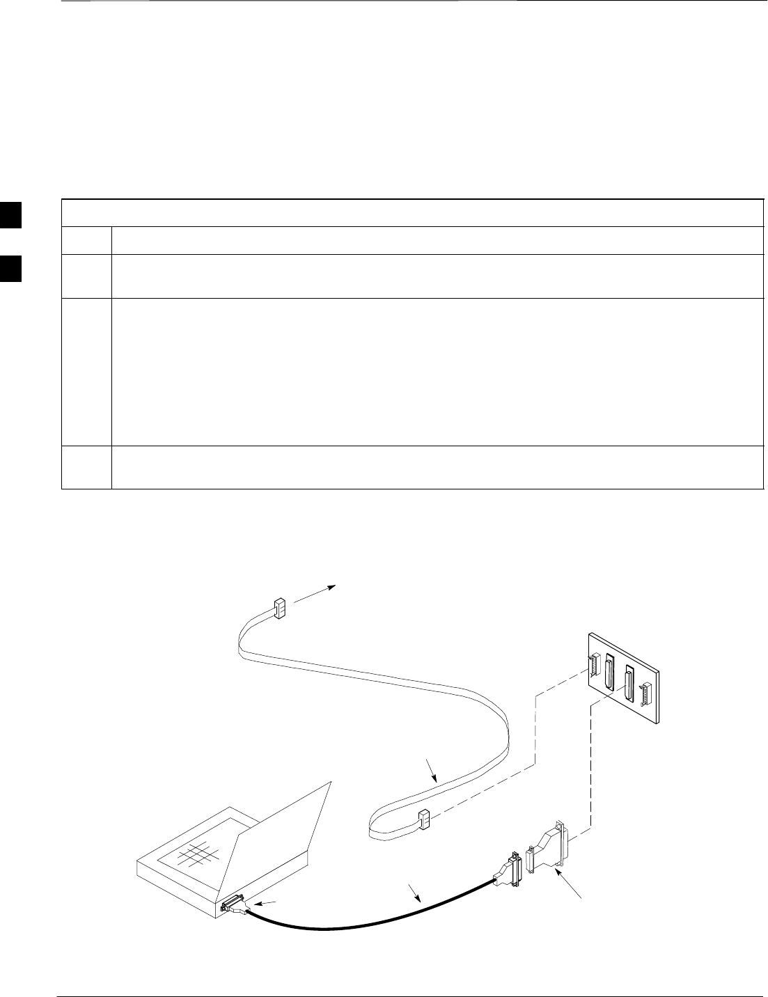
Pinging the Processors
For proper operation, the integrity of the Ethernet LAN A and B links
must be be verified. Figure 3-5 represents a typical BTS Ethernet
configuration. The drawing depicts one (of two identical) links, A and B.
Ping is a program that sends request packets to the LAN network
modules to get a response from the specified “target” module.
Follow the steps in Table 3-7 to ping each processor (on both LAN A
and LAN B) and verify LAN redundancy is working properly.
Always wear a conductive, high impedance wrist strap
while handling any circuit card/module to prevent damage
by ESD.
CAUTION
RF Expansion Ports
Punch
Block Power Input
27V Ret
Antenna’s
1A 2A 3A 1B 2B 3B
4A 5A 6A 4B 5B 6B
1A 2A 3A 1B 2B 3B
4A 5A 6A 4B 5B 6B
1
2
Remote
ASU
GND
Lugs
50 Pair
(Alarms/
Punchblock
20 Pair
(RGPS)
RGD
Board
RGD/RGPS
Power Input
+27V
Micro–
wave
RF
GPS
A
B
IN OUT
LAN
19 MHz
2 Sec
Spans
Alams
Modem
Spans)
CHASSIS
GROUND
SIGNAL
GROUND
50Ω
SIGNAL
GROUND
50Ω
IN
BTS
(MASTER)
OUT
BTS
(EXPANSION)
CHASSIS
GROUND
SIGNAL
GROUND
50Ω
SIGNAL
GROUND
50Ω
FW00199
Figure 3-5: BTS Ethernet LAN Interconnect Diagram
3
Preparing the LMF – continued
DRAFT
SCt4812ET BTS Optimization/ATP — CDMA LMF Apr 2001
3-20
*The Ethernet LAN A and B cables must be installed on
each frame/enclosure before performing this test. All other
processor board LAN connections are made via the
backplanes.
IMPORTANT
Table 3-7: Pinging the Processors
Step Action
1From the Windows desktop, click the Start button and select Run.
2In the Open box, type ping and the GLI2 IP address (for example, ping 128.0.0.2).
NOTE
128.0.0.2 is the default IP address for the GLI2 in field BTS units.
3Click on the OK button.
4If the targeted module responds, text similar to the following is displayed:
Reply from 128 128.0.0.2: bytes=32 time=3ms TTL=255
If there is no response the following is displayed:
Request timed out
If the GLI2 fails to respond, it should be reset and re–pinged. If it still fails to respond, typical
problems are shorted BNC to inter-frame cabling, open cables, crossed A and B link cables, or the
GLI2 itself.
3

Using CDMA LMF
DRAFT
Apr 2001 3-21
SCt4812ET BTS Optimization/ATP — CDMA LMF
Basic LMF Operation
The terms “CDMA LMF” and “WinLMF” are
interchangeable
NOTE
The CDMA LMF allows the user to work in the two following operating
environments which are accessed using the specified desktop icon:
SGraphical User Interface (GUI) using the WinLMF icon
SCommand Line Interface (CLI) using the WinLMF CLI icon
The GUI is the primary optimization and acceptance testing operating
environment. The CLI environment provides additional capability to the
user to perform manually controlled acceptance tests and audit the
results of optimization and calibration actions.
Basic operation of the LMF GUI includes the following:
SSelecting and deselecting BTS devices
SEnabling devices
SDisabling devices
SResetting devices
SObtaining device status
SSorting a status report window
For detailed information on performing these and other LMF operations,
refer to the CDMA LMF Operator’s Guide, 68P64114A78.
Basic LMF Command Line
Interface (CLI) Operation
.
Both the GUI and the CLI use a program known as the handler. Only one
handler can be running at one time. The architectural design is such that
the GUI must be started before the CLI if you want the GUI and CLI to
use the same handler. When the CLI is launched after the GUI, the CLI
automatically finds and uses an in–progress login session with a BTS
initiated under the GUI. This allows the use of the GUI and the CLI in
the same BTS login session. If a CLI handler is already running when
the GUI is launched (this happens if the CLI window is already running
when the user starts the GUI, or if another copy of the GUI is already
running when the user starts the GUI), a dialog window displays the
following warning message:
The CLI handler is already running.
This may cause conflicts with the LMF.
Are you sure that you want to start the application?
This window also contains yes and no buttons. Selecting yes starts the
application. Selecting no terminates the application.
3
Using CDMA LMF – continued
DRAFT
SCt4812ET BTS Optimization/ATP — CDMA LMF Apr 2001
3-22
CLI Format Conventions
The CLI command can be broken down in the following way:
Sverb
Sdevice including device identifier parameters
Sswitch
Soption parameters consisting of:
– keywords
–equals sign (=) between the keyword and the parameter value
–parameter values
Spaces are required between the verb, device, switch, and option
parameters. A hyphen is required between the device and its identifiers.
Following is an example of a CLI command.
measure bbx–<bts_id>–<bbx_id> rssi channel=6 sector=5
Refer to the LMF CLI Commands, R 15.X (68P09251A59) for a
complete explanation of the CLI commands and their use.
Logging into a BTS
Be sure that the correct bts–#.cdf and cbsc–#.cdf file is
used for the BTS. These should be the CDF files that are
provided for the BTS by the CBSC. Failure to use the
correct CDF files can result in wrong results. Failure to
use the correct CDF files to log into a live (traffic
carrying) site can shut down the site.
IMPORTANT
*
Logging into a BTS establishes a communications link between the BTS
and the CDMA LMF. You may be logged into one or more BTS’s at a
time, but only one LMF may be logged into each BTS.
Before attempting to log into the BTS, confirm the CDMA LMF is
properly connected to the BTS (see Figure 3-4). Follow the procedure in
Table 3-8 to log into a BTS.
Prerequisites
Before attempting to login to a BTS, ensure the following have been
completed:
SThe LMF is correctly installed and prepared.
SA bts-nnn folder with the correct CDF and CBSC file exists.
SThe LMF is correctly installed and prepared, and the LMF computer
was connected to the BTS before starting the Windows operating
system and LMF software. If necessary, restart the computer after
connecting it to the BTS (see Table 3-6 and Figure 3-4).
3

Using CDMA LMF – continued
DRAFT
Apr 2001 3-23
SCt4812ET BTS Optimization/ATP — CDMA LMF
BTS Login from the GUI Environment
Follow the procedures in Table 3-8 to log into a BTS when using the
GUI environment
Table 3-8: BTS GUI Login Procedure
Step Action
1Start the LMF GUI environment by clicking on the WinLMF desktop icon (if the LMF’s not running).
NOTE
If a warning similar to the following is displayed, select No, shut down other LMF sessions which
may be running, and start the LMF GUI environment again:
The CLI handler is already running.
This may cause conflicts with the LMF
Are you sure you want to start the application?
Yes No
2Click on Login tab (if not displayed).
3If no base stations are displayed in the Available Base Stations pick list, double click on the CDMA
icon.
4Click on the desired BTS number.
5Click on the Network Login tab (if not already in the forefront).
6Enter correct IP address (normally 128.0.0.2 for a field BTS) if not correctly displayed in the IP
Address box.
NOTE
128.0.0.2 is the default IP address for MGLI–1 in field BTS units. 128.0.0.1 is the default IP address
for MGLI–2.
7Type in the correct IP Port number (normally 9216) if not correctly displayed in the IP Port box.
8Change the Multi-Channel Preselector (from the Multi-Channel Preselector pick list), normally
MPC, corresponding to your BTS configuration, if required.
9Click on the Use a Tower Top Amplifier, if applicable.
10 Click on Login. (A BTS tab with the BTS is displayed.)
NOTE
SIf you attempt to log in to a BTS that is already logged on, all devices will be gray.
SThere may be instances where the BTS initiates a log out due to a system error (i.e., a device
failure).
SIf the MGLI is OOS_ROM (blue), it will have to be downloaded with code before other devices can
be seen.
SIf the MGLI is OOS–RAM (yellow), it must be enabled before other installed devices can be seen.
3
Using CDMA LMF – continued
DRAFT
SCt4812ET BTS Optimization/ATP — CDMA LMF Apr 2001
3-24
BTS Login from the CLI Environment
Follow the procedures in Table 3-9 to log into a BTS when using the
GUI environment
Table 3-9: BTS CLI Login Procedure
Step Action
1Double click the WinLMF CLI desktop icon (if the LMF CLI environment is not already running).
NOTE
If a BTS was logged into under a GUI session when the CLI environment was started, the CLI session
will be logged into the same BTS, and step 2 is not required.
2At the /wlmf prompt, enter the following command:
login bts–<bts#> host=<host> port=<port>
where:
host = MGLI card IP address (defaults to address last logged into for this BTS or 128.0.0.2 if this is
first login to this BTS).
port = IP port of the TS (defaults to port last logged into for this BTS or 9216 if this is first login to
this BTS)
Logging Out
Logging out of a BTS is accomplished differently for the GUI and the
CLI operating environments.
The GUI and CLI environments use the same connection to
a BTS. If a BTS is logged into in both the GUI and the CLI
environments at the same time, logging out of the BTS in
either environment will log out of it for both. When either
a login or logout is performed in the CLI window, there is
no GUI indication that the login or logout has occurred.
IMPORTANT
*
Logging Out of a BTS from the GUI Environment
Follow the procedure in Table 3-10 to logout of a BTS when using the
GUI environment.
Table 3-10: BTS GUI Logout Procedure
Step Action
1Click on Select on the BTS tab menu bar.
2Click the Logout item in the pulldown menu (a Confirm Logout pop–up message will appear).
. . . continued on next page
3

Using CDMA LMF – continued
DRAFT
Apr 2001 3-25
SCt4812ET BTS Optimization/ATP — CDMA LMF
Table 3-10: BTS GUI Logout Procedure
Step Action
3Click on Yes or press the Enter key to confirm logout. You are returned to the Login tab.
NOTE
If a logout was previously performed on the BTS from a CLI window running at the same time as the
GUI, a Logout Error popup message will appear stating the system should not log out of the BTS.
When this occurs, the GUI must be exited and restarted before it can be used for further operations.
4If a Logout Error popup message appears stating that the system could not log out of the Base Station
because the given BTS is not logged in, click OK and proceed to step 5.
5 Select File > Exit in the window menu bar, click Yes in the Confirm Logout popup, and click Yes in
the Logout Error popup which appears again.
6If further work is to be done in the GUI, restart it.
Logging Out of a BTS from the CLI Environment
Follow the procedure in Table 3-10 to logout of a BTS when using the
CLI environment.
Table 3-11: BTS CLI Logout Procedure
Step Action
1
* IMPORTANT
If the BTS is also logged into from a GUI running at the same time and further work must be done
with it in the GUI, proceed to step 2.
Logout of a BTS by entering the following command:
logout bts– <bts#>
A response similar to the following will be displayed:
LMF>
12:22:58.028 Command Received and Accepted
Command=logout bts–33
12:22:58.028 Command Received and Accepted
12:22:58.028 Command Successfully Completed
REASON_CODE=”No Reason”
2If desired, close the CLI interface by entering the following command:
exit
A response similar to the following will be displayed before the window closes:
Killing background processes....
3
Using CDMA LMF – continued
DRAFT
SCt4812ET BTS Optimization/ATP — CDMA LMF Apr 2001
3-26
Establishing an MMI
Communication Session
For those procedures that require MMI communications between the
LMF and BTS FRUs, follow the procedure in Table 3-12 to initiate the
communication session.
Table 3-12: Establishing MMI Communications
Step Action
1Connect the LMF computer to the equipment as detailed in the applicable procedure that requires
MMI communication session.
2Start the named HyperTerminal connection for MMI sessions by double clicking on its Windows
desktop shortcut.
NOTE
If a Windows desktop shortcut was not created for the MMI connection, access the connection from
the Windows Start menu by selecting:
Programs>Accessories>Hyperterminal>HyperTerminal><Named HyperTerminal Connection
(e.g., MMI Session).
3Once the connection window opens, establish MMI communication with the BTS FRU by pressing
the LMF computer Enter key until the prompt identified in the applicable procedure is obtained.
NULL MODEM
BOARD
(TRN9666A)
8–PIN TO 10–PIN
RS–232 CABLE (P/N
30–09786R01)
RS–232 CABLE
8–PIN
CDMA LMF
COMPUTER
To FRU MMI port
DB9–TO–DB25
ADAPTER
Figure 3-6: CDMA LMF Computer Common MMI Connections
COM1
OR
COM2
FW00687
3
Download the BTS
Apr 2001 3-27
SCt4812ET BTS Optimization/ATP — CDMA LMF
DRAFT
Download Code
Code can be downloaded to a device that is in any state. After the
download starts, the device being downloaded changes to
OOS_ROM (blue). If the download is completed successfully, the device
changes to OOS_RAM with code loaded (yellow). Prior to downloading
a device, a code file must exist. The code file is selected automatically if
the code file is in the /lmf/cdma/n.n.n.n/code folder (where n.n.n.n is the
version number of the download code that matches the “NextLoad”
parameter in the CDF file). The code file in the code folder must have
the correct hardware bin number. Code can be automatically or manually
selected.
The following are the devices to be downloaded:
SSpan Configuration
–Master Group Line Interface (MGLI2)
–Slave Group Line Interface (SGLI2)
SClock Synchronization Manager (CSM)
SMulti Channel Card (MCC24E or MCC8E)
SBroadband Transceiver (BBX2)
STest Subscriber Interface Card (TSIC) – if RFDS is installed
The MGLI must be successfully downloaded with code and
data, and put INS before downloading any other device.
The download code process for an MGLI automatically
downloads data and enables the MGLI before downloading
other devices. The other devices can be downloaded in any
order.
IMPORTANT
*
Follow the procedure in Table 3-13 to download the firmware
application code for the MGLI2. The download code action downloads
data and also enables the MGLI2.
Prerequisites
Prior to performing these procedures, ensure a code file exists for each of
the devices to be downloaded.
3
Download the BTS – continued
DRAFT
SCt4812ET BTS Optimization/ATP — CDMA LMF Apr 2001
3-28
All devices in a BTS must have the same R–level ROM
and RAM code before the optimization and ATP
procedures can be performed. If a newly installed BTS is to
be upgraded, the optimization and ATPs should be
accomplished with the prior code load. Then the site
should be upgraded by the CBSC. The optimization and
ATP procedures do not have to be performed again after
the upgrade. If a replacement device needs to be used in a
BTS with a later version of software, the device ROM code
can be changed with use of the LMF before the
optimization and ATPs are performed for the BTS. Refer to
the Download ROM Code section.
WARNING
Table 3-13: Download and Enable MGLI2
Step Action
1 Select Util>Tools>Update Next Load function to ensure the Next Load parameter is set to the correct
code version level.
2Download code to the primary MGLI2 by clicking on the MGLI2.
–From the Device pull down menu, select Download Code.
A status report confirms change in the device(s) status.
– Click OK to close the status window. (The MGLI2 should automatically be downloaded with data
and enabled.)
3Download code and data to the redundant MGLI2 but do not enable at this time.
Download Code and Data to
Non–MGLI2 Devices
Non–MGLI2 devices can be downloaded individually or all equipped
devices can be downloaded with one action. Follow the procedure in
Table 3-14 to download code and data to the non–MGLI2 devices.
When downloading multiple devices, the download may
fail for some of the devices (a time out occurs). These
devices can be downloaded separately after completing the
multiple download.
NOTE
3

Download the BTS – continued
Apr 2001 3-29
SCt4812ET BTS Optimization/ATP — CDMA LMF
DRAFT
Table 3-14: Download Code and Data to Non–MGLI Devices
Step Action
1Select all devices to be downloaded.
2From the Device pull down menu, select Download Code.
A status report displays the result of the download for each selected device.
Click OK to close the status window.
NOTE
After the download has started, the device being downloaded changes to blue. If the download is
completed successfully, the device changes to yellow (OOS-RAM with code loaded).
After a BBX, CSM or MCC is successfully downloaded with code and has changed to OOS-RAM, the
status LED should be rapidly flashing GREEN.
3To download the firmware application data to each device, select the target device and select:
Device>Download Data
Select CSM Clock Source
A CSM can have three different clock sources. The Select CSM Source
function can be used to select the clock source for each of the three
inputs. This function is only used if the clock source for a CSM needs to
be changed. The Clock Source function provides the following clock
source options.
SLocal GPS
SRemote GPS
SHSO (only for source 2 & 3)
SLFR (only for source 2 & 3)
S10 MHz (only for source 2 & 3)
SNONE (only for source 2 & 3)
Prerequisites
MGLI=INS_ACT, CSM= OOS_RAM or INS_ACT
Table 3-15: Select CSM Clock Source
Step Action
1Select the applicable CSM(s).
2Click on the Device menu.
3Click on the Clock Source menu item.
4Click on the Select menu item. A clock source selection window is displayed.
5Select the applicable clock source in the Clock Reference Source pick lists. Uncheck the related
check box if you do not want the displayed pick list item to be used.
6Click on the OK button. A status report window is displayed showing the results of the selection
action.
7Click on the OK button to close the status report window.
3
Download the BTS – continued
DRAFT
SCt4812ET BTS Optimization/ATP — CDMA LMF Apr 2001
3-30
Enable CSMs
Each BTS CSM system features two CSM boards per site. In a typical
operation, the primary CSM locks its Digital Phase Locked Loop
(DPLL) circuits to GPS signals. These signals are generated by either an
on–board GPS module (RF–GPS) or a remote GPS receiver (R–GPS).
The CSM2 card is required when using the R–GPS. The GPS receiver
(mounted on CSM 1) is used as the primary timing reference and
synchronizes the entire cellular system. CSM 2 provides redundancy (but
does not have a GPS receiver).
The BTS may be equipped with a LORAN–C LFR, HSO, or external 10
MHz Rubidium source which the CSM can use as a secondary timing
reference. In all cases, the CSM monitors and determines what reference
to use at a given time.
For RF–GPS, verify the CSM configured with the GPS
receiver “daughter board” is installed in the frame’s CSM 1
slot before continuing.
IMPORTANT
*
Follow the steps outlined in Table 3-16 to enable the CSMs installed in
the C–CCP shelves.
Table 3-16: Enable CSMs
Step Action
1Click on the target CSM.
From the Device pull down, select Enable.
NOTE
If equipped with two CSMs, enable CSM–2 first
A status report is displayed confirming change in the device(s) status.
Click OK to close the status report window.
NOTE
FAIL may be shown in the status table for enable action. If Waiting For Phase Lock is shown in the
Description field, the CSM changes to the Enabled state after phase lock is achieved.
CSM 1 houses the GPS receiver. The enable sequence can take up to one hour (see below).
* IMPORTANT
The GPS satellite system satellites are not in a geosynchronous orbit and are maintained and operated
by the United States Department of Defense (D.O.D.). The D.O.D. periodically alters satellite orbits;
therefore, satellite trajectories are subject to change. A GPS receiver that is INS contains an “almanac”
that is updated periodically to take these changes into account.
If a GPS receiver has not been updated for a number of weeks, it may take up to an hour for the GPS
receiver “almanac” to be updated.
Once updated, the GPS receiver must track at least four satellites and obtain (hold) a 3–D position fix
for a minimum of 45 seconds before the CSM will come in service. (In some cases, the GPS receiver
needs to track only one satellite, depending on accuracy mode set during the data load).
. . . continued on next page
3
Download the BTS – continued
Apr 2001 3-31
SCt4812ET BTS Optimization/ATP — CDMA LMF
DRAFT
Table 3-16: Enable CSMs
Step Action
2NOTE
If equipped with two CSMs, CSM–1 should be bright green (INS–ACT) and CSM–2 should be dark
green(INS–STB)
If more than an hour has passed, refer to CSM Verification, see Figure 3-7 and Table 3-19 to determine
the cause.
NOTE
After the CSMs have been successfully enabled, observe the PWR/ALM LEDs are steady green
(alternating green/red indicates the card is in an alarm state).
Enable MCCs
This procedure configures the MCC and sets the “tx fine adjust”
parameter. The “tx fine adjust” parameter is not a transmit gain setting,
but a timing adjustment that compensates for the processing delay in the
BTS (approximately 3 mS).
Follow the steps outlined in Table 3-17 to enable the MCCs installed in
the C–CCP shelves.
The MGLI and CSM must be downloaded and enabled,
prior to downloading and enabling the MCC.
IMPORTANT
*
Table 3-17: Enable MCCs
Step Action
1Click on the target MCC(s) or from the Select pull down menu choose All MCCs.
2From the Device menu, select Enable
A status report is displayed confirming change in the device(s) status.
3 Click OK to close the status report window.
3

CSM System Time – GPS & LFR/HSO Verification
DRAFT
SCt4812ET BTS Optimization/ATP — CDMA LMF Apr 2001
3-32
Clock Synchronization
Manager System Time
The primary function of the Clock Synchronization Manager (CSM)
boards (slots 1 and 2) is to maintain CDMA system time. The CSM in
slot 1 is the primary timing source while slot 2 provides redundancy.
The CSM2 card (CSM second generation) is required when using the
remote GPS receiver (R–GPS). R–GPS uses a GPS receiver in the
antenna head that has a digital output to the CSM2 card. CSM2 can have
a daughter card as a local GPS receiver to support an RF–GPS signal.
The CSM2 switches between the primary and redundant units (slots 1
and 2) upon failure or command. CDMA Clock Distribution Cards
(CCDs) buffer and distribute even–second reference and 19.6608 MHz
clocks. CCD 1 is married to CSM 1 and CCD 2 is married to CSM 2. A
failure on CSM 1 or CCD 1 cause the system to switch to redundant
CSM 2 and CCD 2.
Each CSM2 board features an ovenized, crystal oscillator that provides
19.6608 MHz clock, even second pulse, and 3 MHz referenced to the
selected synchronization source (see Table 3-19):
SGPS: local/RF–GPS or remote/R–GPS
SLORAN–C Frequency Receiver (LFR) or High Stability Oscillator
(HSO)
SExternal reference oscillator sources
Fault management has the capability of switching between the GPS
synchronization source and the LFR/HSO backup source in the event of
a GPS receiver failure on CSM 1. During normal operation, the CSM 1
board selects GPS as the primary source (see Table 3-19). The source
selection can also be overridden via the LMF or by the system software.
Synchronization between the primary and redundant CSM CCD pairs, as
well as the LFR or HSO back–up to GPS synchronization, increases
reliability.
Low Frequency Receiver/
High Stability Oscillator
The CSM handles the overall configuration and status monitoring
functions of the LFR/HSO. In the event of GPS failure, the LFR/HSO is
capable of maintaining synchronization initially established by the GPS
reference signal.
The LFR requires an active external antenna to receive LORAN RF
signals. Timing pulses are derived from this signal, which is
synchronized to Universal Time Coordinates (UTC) and GPS time. The
LFR can maintain system time indefinately after initial GPS lock.
3

CSM System Time – GPS & LFR/HSO Verification – continued
Apr 2001 3-33
SCt4812ET BTS Optimization/ATP — CDMA LMF
DRAFT
The HSO is a high stability 10 MHz oscillator with the necessary
interface to the CSMs. The HSO is typically installed in those
geographical areas not covered by the LORAN–C system. Since the
HSO is a free–standing oscillator, system time can only be maintained
for 24 hours after 24 hours of GPS lock.
Upgrades and Expansions: LFR2/HSO2/HSOX
LFR2/HSO2 (second generation cards) both export a timing signal to the
expansion or logical BTS frames. The associated expansion or logical
frames require an HSO–expansion (HSOX) whether the starter frame has
an LFR2 or an HSO2. The HSOX accepts input from the starter frame
and interfaces with the CSM cards in the expansion frame. LFR and
LFR2 use the same source code in source selection (see Table 3-19).
HSO, HSO2, and HSOX use the same source code in source selection
(see Table 3-19).
Allow the base site and test equipment to warm up for
60 minutes after any interruption in oscillator power.
CSM board warm-up allows the oscillator oven
temperature and oscillator frequency to stabilize prior to
test. Test equipment warm-up allows the Rubidium
standard timebase to stabilize in frequency before any
measurements are made.
NOTE
3
CSM System Time – GPS & LFR/HSO Verification – continued
DRAFT
SCt4812ET BTS Optimization/ATP — CDMA LMF Apr 2001
3-34
CSM Frequency Verification
The objective of this procedure is the initial verification of the CSM
boards before performing the rf path verification tests. Parts of this
procedure will be repeated for final verification after the overall
optimization has been completed.
Test Equipment Setup
(GPS & LFR/HSO Verification)
Follow the steps outlined in Table 3-18 to set up test equipment.
Table 3-18: Test Equipment Setup (GPS & LFR/HSO Verification)
Step Action
1a For local GPS (RF–GPS): Verify a CSM board with a GPS receiver is installed in primary CSM slot 1
and that CSM–1 is INS.
NOTE
This is verified by checking the board ejectors for kit number SGLN1145 on the board in slot 1.
1b For Remote GPS (RGPS):Verify a CSM2 board is installed in primary slot 1 and that CSM–1 is INS.
NOTE
This is verified by checking the board ejectors for kit number SGLN4132CC (or subsequent).
2Remove CSM–2 (if installed) and connect a serial cable from the LMF COM 1 port (via null modem
board) to the MMI port on CSM–1 (see Figure 3-7).
3Reinstall CSM–2.
4Start an MMI communication session with CSM–1 by using the Windows desktop shortcut icon (see
Table 3-5)
NOTE
The LMF program must be running when a Hyperterminal session is started.
5When the terminal screen appears press the Enter key until the CSM> prompt appears.
SConnect GPS antenna to the (GPS) RF connector
ONLY. Damage to the GPS antenna and/or receiver
can result if the GPS antenna is inadvertently connected
to any other RF connector.
CAUTION
3
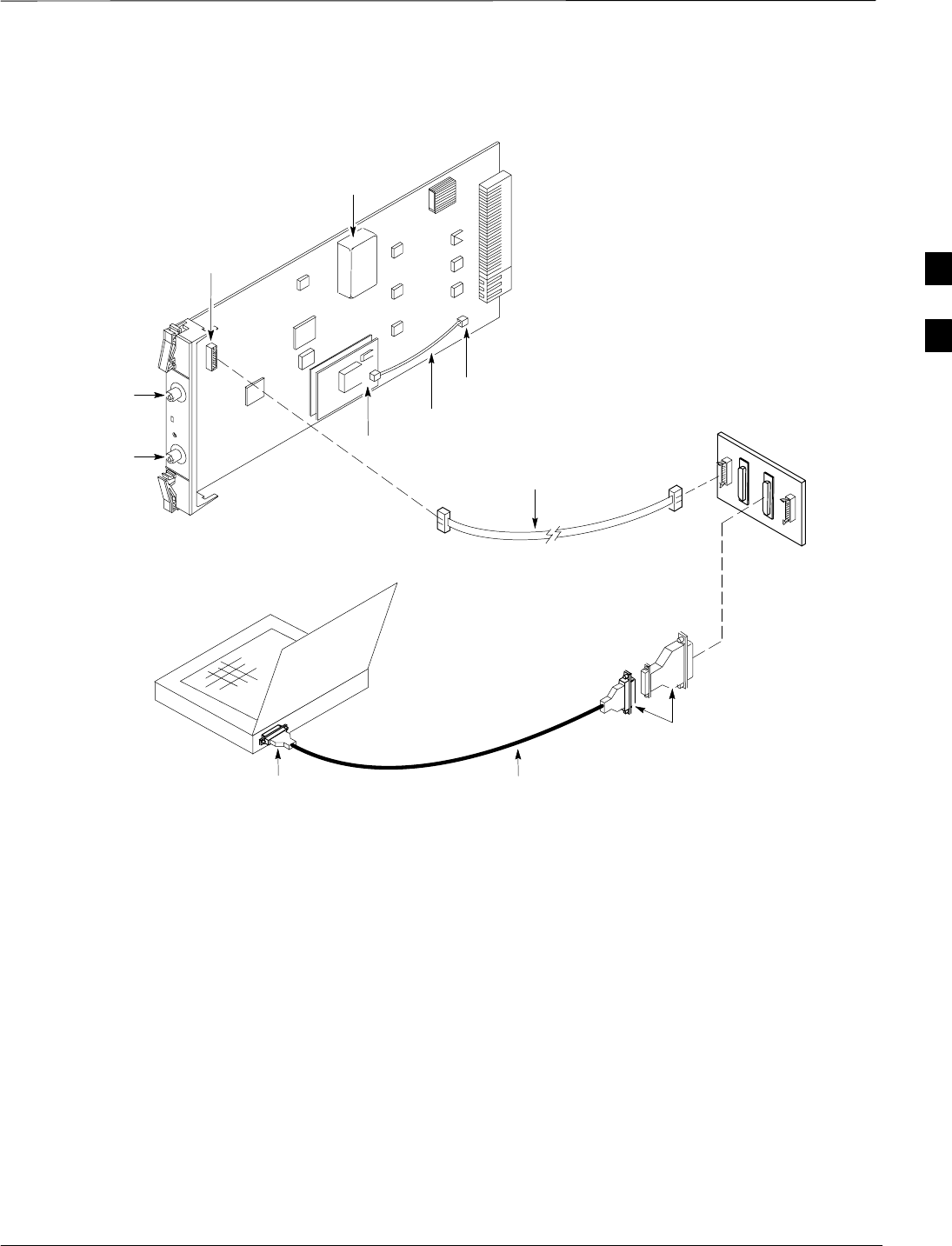
CSM System Time – GPS & LFR/HSO Verification – continued
Apr 2001 3-35
SCt4812ET BTS Optimization/ATP — CDMA LMF
DRAFT
NULL MODEM
BOARD
(TRN9666A)
RS–232 SERIAL
MODEM CABLE
DB9–TO–DB25
ADAPTER
COM1
LMF
NOTEBOOK
Figure 3-7: CSM MMI Terminal Connection
FW00372
CSM board shown
removed from frame
19.6 MHZ TEST
POINT REFERENCE
(NOTE 1)
EVEN SECOND
TICK TEST POINT
REFERENCE
GPS RECEIVER
ANTENNA INPUT
GPS RECEIVER
MMI SERIAL
PORT
ANTENNA COAX
CABLE
REFERENCE
OSCILLATOR
9–PIN TO 9–PIN
RS–232 CABLE
NOTES:
1. One LED on each CSM:
Green = IN–SERVICE ACTIVE
Fast Flashing Green = OOS–RAM
Red = Fault Condition
Flashing Green & Red = Fault
GPS Initialization/Verification
Follow the steps outlined in Table 3-19 to connect to CSM–1 installed in
the C–CCP shelf, verifying that it is functioning normally.
3

CSM System Time – GPS & LFR/HSO Verification – continued
DRAFT
SCt4812ET BTS Optimization/ATP — CDMA LMF Apr 2001
3-36
Table 3-19: GPS Initialization/Verification
Step Action
1To verify that Clock alarms (0000), Dpll is locked and has a reference source, and
GPS self test passed messages are displayed within the report, issue the following MMI
command
bstatus
–Observe the following typical response:
CSM Status INS:ACTIVE Slot A Clock MASTER.
BDC_MAP:000, This CSM’s BDC Map:0000
Clock Alarms (0000):
DPLL is locked and has a reference source.
GPS receiver self test result: passed
Time since reset 0:33:11, time since power on: 0:33:11
2Enter the following command at the CSM> prompt to display the current status of the Loran and the
GPS receivers.
sources
–Observe the following typical response for systems equipped with LFR:
N Source Name Type TO Good Status Last Phase Target Phase Valid
–––––––––––––––––––––––––––––––––––––––––––––––––––––––––––––––––––––––––
0LocalGPS Primary 4 YES Good 00Yes
1 LFR CHA Secondary 4 YES Good –2013177 –2013177 Yes
2 Not Used
Current reference source number: 0
–Observe the following typical response for systems equipped with HSO:
Num Source Name Type TO Good Status Last Phase Target Phase Valid
––––––––––––––––––––––––––––––––––––––––––––––––––––––––––––––––––––––––––––
0 Local GPS Primary 4 Yes Good 3 0 Yes
1HSO Backup 4 No N/A timed–out* Timed–out* No
*NOTE “Timed–out” should only be displayed while the HSO is warming up. “Not–Present” or
“Faulty” should not be displayed. If the HSO does not appear as one of the sources, then configure the
HSO as a back–up source by entering the following command at the CSM> prompt:
ss 1 12
After a maximum of 15 minutes, the Rubidium oscillator should reach operational temperature and the
LED on the HSO should now have changed from red to green. After the HSO front panel LED has
changed to green, enter sources <cr> at the CSM> prompt. Verify that the HSO is now a valid
source by confirming that the bold text below matches the response of the “sources” command.
The HSO should be valid within one (1) minute, assuming the DPLL is locked and the HSO rubidium
oscillator is fully warmed.
Num Source Name Type TO Good Status Last Phase Target Phase Valid
––––––––––––––––––––––––––––––––––––––––––––––––––––––––––––––––––––––––––––
0 Local GPS Primary 4 Yes Good 3 0 Yes
1HSO Backup 4 Yes N/A xxxxxxxxxx xxxxxxxxxx Yes
. . . continued on next page
3

CSM System Time – GPS & LFR/HSO Verification – continued
Apr 2001 3-37
SCt4812ET BTS Optimization/ATP — CDMA LMF
DRAFT
Table 3-19: GPS Initialization/Verification
Step Action
3HSO information (underlined text above, verified from left to right) is usually the #1 reference source.
If this is not the case, have the OMCR determine the correct BTS timing source has been identified in
the database by entering the display bts csmgen command and correct as required using the edit
csm csmgen refsrc command.
* IMPORTANT
If any of the above mentioned areas fail, verify:
–If LED is RED, verify that HSO had been powered up for at least 5 minutes. After oscillator
temperature is stable, LED should go GREEN Wait for this to occur before continuing !
– If “timed out” is displayed in the Last Phase column, suspect the HSO output buffer or oscillator
is defective
–Verify the HSO is FULLY SEATED and LOCKED to prevent any possible board warpage
4Verify the following GPS information (underlined text above):
–GPS information is usually the 0 reference source.
–At least one Primary source must indicate “Status = good” and “Valid = yes” to bring site up.
. . . continued on next page
3

CSM System Time – GPS & LFR/HSO Verification – continued
DRAFT
SCt4812ET BTS Optimization/ATP — CDMA LMF Apr 2001
3-38
Table 3-19: GPS Initialization/Verification
Step Action
5Enter the following command at the CSM> prompt to verify that the GPS receiver is in tracking mode.
gstatus
–Observe the following typical response:
24:06:08 GPS Receiver Control Task State: tracking satellites.
24:06:08 Time since last valid fix: 0 seconds.
24:06:08
24:06:08 Recent Change Data:
24:06:08 Antenna cable delay 0 ns.
24:06:08 Initial position: lat 117650000 msec, lon –350258000 msec, height 0 cm (GPS)
24:06:08 Initial position accuracy (0): estimated.
24:06:08
24:06:08 GPS Receiver Status:
24:06:08 Position hold: lat 118245548 msec, lon –350249750 msec, height 20270 cm
24:06:08 Current position: lat 118245548 msec, lon –350249750 msec, height 20270 cm
(GPS)
24:06:08 8 satellites tracked, receiving 8 satellites, 8 satellites visible.
24:06:08 Current Dilution of Precision (PDOP or HDOP): 0.
24:06:08 Date & Time: 1998:01:13:21:36:11
24:06:08 GPS Receiver Status Byte: 0x08
24:06:08 Chan:0, SVID: 16, Mode: 8, RSSI: 148, Status: 0xa8
24:06:08 Chan:1, SVID: 29, Mode: 8, RSSI: 132, Status: 0xa8
24:06:08 Chan:2, SVID: 18, Mode: 8, RSSI: 121, Status: 0xa8
24:06:08 Chan:3, SVID: 14, Mode: 8, RSSI: 110, Status: 0xa8
24:06:08 Chan:4, SVID: 25, Mode: 8, RSSI: 83, Status: 0xa8
24:06:08 Chan:5, SVID: 3, Mode: 8, RSSI: 49, Status: 0xa8
24:06:08 Chan:6, SVID: 19, Mode: 8, RSSI: 115, Status: 0xa8
24:06:08 Chan:7, SVID: 22, Mode: 8, RSSI: 122, Status: 0xa8
24:06:08
24:06:08 GPS Receiver Identification:
24:06:08 COPYRIGHT 1991–1996 MOTOROLA INC.
24:06:08 SFTW P/N # 98–P36830P
24:06:08 SOFTWARE VER # 8
24:06:08 SOFTWARE REV # 8
24:06:08 SOFTWARE DATE 6 AUG 1996
24:06:08 MODEL # B3121P1115
24:06:08 HDWR P/N # _
24:06:08 SERIAL # SSG0217769
24:06:08 MANUFACTUR DATE 6B07
24:06:08 OPTIONS LIST IB
24:06:08 The receiver has 8 channels and is equipped with TRAIM.
6Verify the following GPS information (shown above in underlined text):
–At least 4 satellites are tracked, and 4 satellites are visible.
–GPS Receiver Control Task State is “tracking satellites”. Do not continue until this occurs!
–Dilution of Precision indication is not more that 30.
Record the current position base site latitude, longitude, height and height reference (height reference
to Mean Sea Level (MSL) or GPS height (GPS). (GPS = 0 MSL = 1).
. . . continued on next page
3
CSM System Time – GPS & LFR/HSO Verification – continued
Apr 2001 3-39
SCt4812ET BTS Optimization/ATP — CDMA LMF
DRAFT
Table 3-19: GPS Initialization/Verification
Step Action
7If steps 1 through 6 pass, the GPS is good.
* IMPORTANT
If any of the above mentioned areas fail, verify that:
– If Initial position accuracy is “estimated” (typical), at least 4 satellites must be tracked and
visible (1 satellite must be tracked and visible if actual lat, log, and height data for this site has
been entered into CDF file).
– If Initial position accuracy is “surveyed,” position data currently in the CDF file is assumed to be
accurate. GPS will not automatically survey and update its position.
–The GPS antenna is not obstructed or misaligned.
–GPS antenna connector center conductor measureS approximately +5 Vdc with respect to the
shield.
–There is no more than 4.5 dB of loss between the GPS antenna OSX connector and the BTS frame
GPS input.
–Any lightning protection installed between GPS antenna and BTS frame is installed correctly.
8Enter the following commands at the CSM> prompt to verify that the CSM is warmed up and that GPS
acquisition has taken place.
debug dpllp
Observe the following typical response if the CSM is not warmed up (15 minutes from application of
power) (If warmed–up proceed to step 9)
CSM>DPLL Task Wait. 884 seconds left.
DPLL Task Wait. 882 seconds left.
DPLL Task Wait. 880 seconds left. ...........etc.
NOTE
The warm command can be issued at the MMI port used to force the CSM into warm–up, but the
reference oscillator will be unstable.
9Observe the following typical response if the CSM is warmed up.
c:17486 off: –11, 3, 6 TK SRC:0 S0: 3 S1:–2013175,–2013175
c:17486 off: –11, 3, 6 TK SRC:0 S0: 3 S1:–2013175,–2013175
c:17470 off: –11, 1, 6 TK SRC:0 S0: 1 S1:–2013175,–2013175
c:17486 off: –11, 3, 6 TK SRC:0 S0: 3 S1:–2013175,–2013175
c:17470 off: –11, 1, 6 TK SRC:0 S0: 1 S1:–2013175,–2013175
c:17470 off: –11, 1, 6 TK SRC:0 S0: 1 S1:–2013175,–2013175
10 Verify the following GPS information (underlined text above, from left to right):
–Lower limit offset from tracked source variable is not less than –60 (equates to 3µs limit).
–Upper limit offset from tracked source variable is not more than +60 (equates to 3µs limit).
–TK SRC: 0 is selected, where SRC 0 = GPS.
11 Enter the following commands at the CSM> prompt to exit the debug mode display.
debug dpllp
3

CSM System Time – GPS & LFR/HSO Verification – continued
DRAFT
SCt4812ET BTS Optimization/ATP — CDMA LMF Apr 2001
3-40
LORAN–C
Initialization/Verification
Table 3-20: LORAN–C Initialization/Verification
Step Action Note
1At the CSM> prompt, enter lstatus <cr> to verify that the LFR is in tracking
mode. A typical response is:
CSM> lstatus <cr>
LFR St ti St t
LFR Station Status:
Clock coherence: 512 >
5930M 51/60 dB 0 S/N Flag:
5930X 52/64 dn –1 S/N Flag:
5990 47/55 dB –6 S/N Flag:
7980M 62/66 dB 10 S/N Fl
This must be greater
than 100 before LFR
becomes a valid source.
7980M 62/66 dB 10 S/N Flag:
7980W 65/69 dB 14 S/N Flag: . PLL Station . >
7980X 48/54 dB –4 S/N Flag:
7980Y 46/58 dB –8 S/N Flag:E
7980Z 60/67 dB 8 S/N Flag:
8290M 50/65 dB 0 S/N Flag
This shows the LFR is
locked to the selected
PLL station.
8290M 50/65 dB 0 S/N Flag:
8290W 73/79 dB 20 S/N Flag:
8290W 58/61 dB 6 S/N Flag:
8290W 58/61 dB 6 S/N Flag:
8970M 89/95 dB 29 S/N Flag:
8970W 62/66 dB 10 S/N Flag:
8970X 73/79 dB 22 S/N Flag:
8970X 73/79 dB 22 S/N Fl
ag:
8970Y 73/79 dB 19 S/N Flag:
8970Z 62/65 dB 10 S/N Flag:
9610M 62/65 dB 10 S/N Fl
g
9610M 62/65 dB 10 S/N Flag:
9610V 58/61 dB 8 S/N Flag:
9610W 47
/
49 dB –4S
/
N Fla
g
:E
9610W 47/49 dB –4 S/N Flag:E
9610X 46/57 dB –5 S/N Flag:E
9610Y 48/54 dB –5 S/N Flag:E
9610Z 65/69 dB 12 S/N Flag
9610Z 65/69 dB 12 S/N Flag:
9940M 50/53 dB –1 S/N Flag:S
9940W 49/56 dB –4 S/N Flag:E
9940W 49/56 dB 4 S/N Flag:E
9940Y 46/50 dB–10 S/N Flag:E
9960M 73/79 dB 22 S/N Flag:
9960W 51/60 dB 0 S/N Flag:
9960W 51/60 dB 0 S/N Fl
ag:
9960X 51/63 dB –1 S/N Flag:
9960Y 59/67 dB 8 S/N Flag:
9960Z 89/96 dB 29 S/N Fl
9960Z 89/96 dB 29 S/N Flag:
LFR Task State: lfr locked to station 7980W
LFR Recent Change Data:
Search List: 5930 5990 7980 8290 8970 9940 9610 9960 >
PLL GRI: 7980W
LFR Master, reset not needed, not the reference source.
CSM>
This search list and PLL
data must match the
configuration for the
geographical location
of the cell site.
. . . continued on next page
3
CSM System Time – GPS & LFR/HSO Verification – continued
Apr 2001 3-41
SCt4812ET BTS Optimization/ATP — CDMA LMF
DRAFT
Table 3-20: LORAN–C Initialization/Verification
Step NoteAction
2Verify the following LFR information (highlighted above in boldface type):
–Locate the “dot” that indicates the current phase locked station assignment (assigned by MM).
–Verify that the station call letters are as specified in site documentation as well as M X Y Z
assignment.
–Verify the S/N ratio of the phase locked station is greater than 8.
3At the CSM> prompt, enter sources <cr> to display the current status of the the LORAN receiver.
–Observe the following typical response.
Num Source Name Type TO Good Status Last Phase Target Phase Valid
––––––––––––––––––––––––––––––––––––––––––––––––––––––––––––––––––––––––––––
0 Local GPS Primary 4 Yes Good –3 0 Yes
1 LFR ch A Secondary 4 Yes Good –2013177 –2013177 Yes
2 Not used
Current reference source number: 1
4LORAN LFR information (highlighted above in boldface type) is usually the #1 reference source
(verified from left to right).
* IMPORTANT
If any of the above mentioned areas fail, verify:
–The LFR antenna is not obstructed or misaligned.
–The antenna pre–amplifier power and calibration twisted pair connections are intact and < 91.4 m
(300 ft) in length.
–A dependable connection to suitable Earth Ground is in place.
–The search list and PLL station for cellsite location are correctly configured .
NOTE
LFR functionality should be verified using the “source” command (as shown in Step 3). Use the
underlined responses on the LFR row to validate correct LFR operation.
5Close the hyperterminal window.
3

Test Equipment Set–up
DRAFT
SCt4812ET BTS Optimization/ATP — CDMA LMF Apr 2001
3-42
Connecting Test Equipment to
the BTS
All test equipment is controlled by the LMF via IEEE–488/GPIB bus.
The LMF requires each piece of test equipment to have a factory set
GPIB address. If there is a communications problem between the LMF
and any piece of test equipment, verify that the GPIB addresses have
been set correctly (normally 13 for a power meter and 18 for a CDMA
analyzer).
The following test equipment is required to perform optimization,
calibration and ATP tests:
SLMF
STest set
SDirectional coupler and attenuator
SRF cables and connectors
Refer to Table 3-21 for an overview of connections for test equipment
currently supported by LMF. In addition, see the following figures:
SFigure 3-9 and Figure 3-10 show the test set connections for TX
calibration
SFigure 3-11 and Figure 3-12 show the test set connections for
optimization/ATP tests
Supported Test Sets
Optimization and ATP testing may be performed using one of the
following test sets:
SCyberTest
SAdvantest R3465 and HP–437B or Gigatronics Power Meter
SHewlett–Packard HP 8935
SHewlett–Packard HP 8921 (W/CDMA and PCS Interface (1.9 GHz)
and HP–437B or Gigatronics Power Meter
SSpectrum Analyzer (HP8594E) – optional
SRubidium Standard Timebase – optional
To prevent damage to the test equipment, all TX test
connections must be through the 30 dB directional coupler
for an 800 MHz BTS and the 30 dB directional coupler
plus a 20 dB in-line attenuator for a 1.9 GHz BTS.
CAUTION
3
Test Equipment Set–up – continued
Apr 2001 3-43
SCt4812ET BTS Optimization/ATP — CDMA LMF
DRAFT
Test Equipment Setup Chart
Table 3-21 depicts the current test equipment available meeting Motorola
standards.
To identify the connection ports, locate the test equipment presently
being used in the TEST SETS columns, and read down the column.
Where a ball appears in the column, connect one end of the test cable to
that port. Follow the horizontal line to locate the end connection(s),
reading up the column to identify the appropriate equipment/BTS port.
Table 3-21: Test Equipment Setup
TEST SETS ADDITIONAL TEST EQUIPMENT
SIGNAL Cyber–
Test Ad-
vantest HP
8935 HP
8921A
HP
8921
W/PCS Power
Meter
GPIB
Inter-
face LMF Directional
Coupler & Pad* BTS
EVEN SECOND
SYNCHRONIZATION EVEN
SEC REF EVEN SEC
SYNC IN
EVEN
SECOND
SYNC IN
EVEN
SECOND
SYNC IN
EVEN
SECOND
SYNC IN
19.6608 MHZ
CLOCK TIME
BASE IN
CDMA
TIME BASE
IN EXT
REF IN
CDMA
TIME BASE
IN
CDMA
TIME BASE
IN
CONTROL
IEEE 488 BUS IEEE
488 GPIB HP–IB HP–IB GPIB SERIAL
PORT
HP–IB HP–IB
TX TEST
CABLES RF
IN/OUT INPUT
50–OHM RF
IN/OUT TX1–6
RF
IN/OUT RF
IN/OUT 20 DB
PAD BTS
PORT
RX TEST
CABLES RF IN/
OUT RF OUT
50–OHM DUPLEX RX1–12
DUPLEX
OUT RF OUT
ONLY
SYNC
MONITOR
FREQ
MONITOR
3
Test Equipment Set–up – continued
DRAFT
SCt4812ET BTS Optimization/ATP — CDMA LMF Apr 2001
3-44
Equipment Warm-up
Warm-up BTS equipment for a minimum of 60 minutes
prior to performing the BTS optimization procedure. This
assures BTS site stability and contributes to optimization
accuracy. (Time spent running initial power-up,
hardware/firmware audit, and BTS download counts as
warm-up time.)
IMPORTANT
*
Before installing any test equipment directly to any BTS
TX OUT connector, verify there are NO CDMA BBX
channels keyed. At active sites, have the OMC-R/CBSC
place the antenna (sector) assigned to the LPA under test
OOS. Failure to do so can result in serious personal injury
and/or equipment damage.
WARNING
Cable Calibration Setup
Figure 3-8 shows the cable calibration setup for various supported test
sets. The left side of the diagram depicts the location of the input and
output ports of each test set, and the right side details the set up for each
test. Table 3-25 provides a procedure for calibrating cables.
3
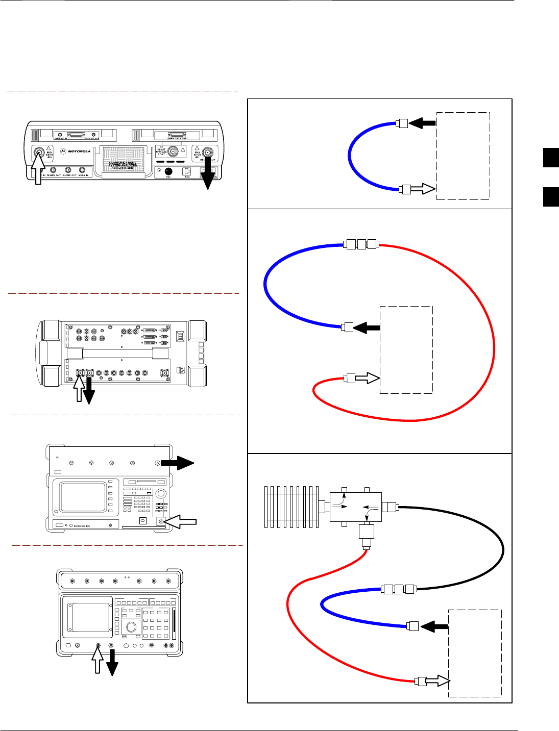
Test Equipment Set–up – continued
Apr 2001 3-45
SCt4812ET BTS Optimization/ATP — CDMA LMF
DRAFT
Motorola CyberTest
Hewlett–Packard Model HP 8935
Advantest Model R3465
DUPLEX
OUT
RF OUT
50–OHM
INPUT
50–OHM
RF GEN OUTANT IN
ANT
IN
SUPPORTED TEST SETS
100–WATT (MIN)
NON–RADIATING
RF LOAD
TEST
SET
A. SHORT CABLE CAL
SHORT
CABLE
B. RX TEST SETUP
TEST
SET
C. TX TEST SETUP
20 DB PAD
FOR 1.9 GHZ
CALIBRATION SET UP
N–N FEMALE
ADAPTER
TX
CABLE
TX
CABLE
SHORT
CABLE
Note: The Directional Coupler is not used with the
Cybertest Test Set. The TX cable is connected
directly to the Cybertest Test Set.
A 10dB attenuator must be used with the short test
cable for cable calibration with the CyberTest Test
Set. The 10dB attenuator is used only for the cable
calibration procedure, not with the test cables for
TX calibration and ATP tests.
TEST
SET
RX
CABLE
SHORT
CABLE
Figure 3-8: Cable Calibration Test Setup
FW00089
Note: For 800 MHZ only. The HP8921A cannot
be used to calibrate cables for PCS frequencies.
Hewlett–Packard Model HP 8921A
DIRECTIONAL COUPLER
(30 DB)
N–N FEMALE
ADAPTER
3
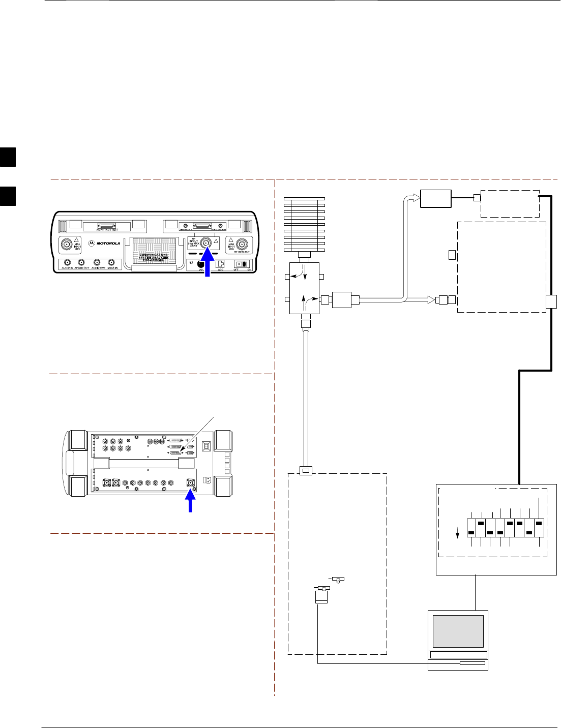
Test Equipment Set–up – continued
DRAFT
SCt4812ET BTS Optimization/ATP — CDMA LMF Apr 2001
3-46
Setup for TX Calibration
Figure 3-9 and Figure 3-10 show the test set connections for TX
calibration.
Motorola CyberTest
Hewlett–Packard Model HP 8935
TEST SETS TRANSMIT (TX) SET UP
FRONT PANEL RF
IN/OUT
RF IN/OUT
HP–IB
TO GPIB
BOX
RS232–GPIB
INTERFACE BOX
INTERNAL PCMCIA
ETHERNET CARD
GPIB
CABLE
COMMUNICATIONS
TEST SET
CONTROL
IEEE 488
GPIB BUS
UNIVERSAL TWISTED
PAIR (UTP) CABLE
(RJ45 CONNECTORS)
RS232
NULL
MODEM
CABLE
OUT
S MODE
DATA FORMAT
BAUD RATE
GPIB ADRS
G MODE
ON
TEST SET
INPUT/
OUTPUT
PORTS
BTS
100–WATT (MIN)
NON–RADIATING
RF LOAD
IN
TX
TEST
CABLE
CDMA
LMF
DIP SWITCH
SETTINGS**
2O DB PAD
FOR 1.9 GHZ
10BASET/
10BASE2
CONVERTER
LAN
B
LAN
A
TX TEST
CABLE
TX ANTENNA
PORT OR TX
RFDS
DIRECTIONAL
COUPLERS
POWER
METER
(OPTIONAL)*
NOTE: THE DIRECTIONAL COUPLER IS NOT USED WITH THE
CYBERTEST TEST SET. THE TX CABLE IS CONNECTED DIRECTLY
TO THE CYBERTEST TEST SET.
* A POWER METER CAN BE USED IN PLACE
OF THE COMMUNICATIONS TEST SET FOR TX
CALIBRATION/AUDIT
POWER
SENSOR
Figure 3-9: TX Calibration Test Setup (CyberTest and HP 8935)
FW00094
DIRECTIONAL COUPLER
(30 DB)
** BLACK PORTION OF THE
DIAGRAM REPRESENTS THE
RAISED PART OF THE
SWITCH
3
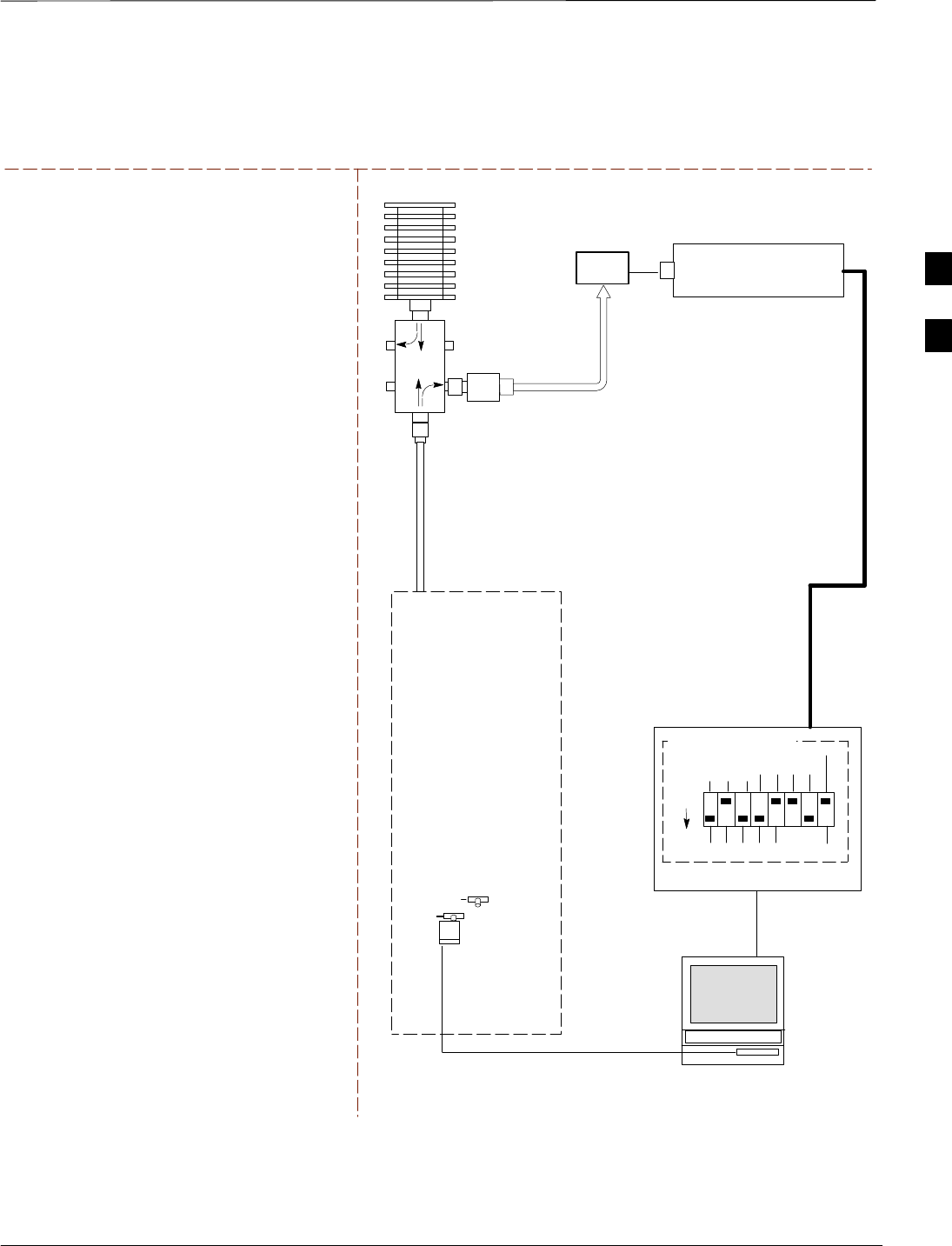
Test Equipment Set–up – continued
Apr 2001 3-47
SCt4812ET BTS Optimization/ATP — CDMA LMF
DRAFT
POWER METER
TEST SETS TRANSMIT (TX) SET UP
RS232–GPIB
INTERFACE BOX
INTERNAL PCMCIA
ETHERNET CARD
GPIB
CABLE
UNIVERSAL TWISTED
PAIR (UTP) CABLE
(RJ45 CONNECTORS)
RS232
NULL
MODEM
CABLE
S MODE
DATA FORMAT
BAUD RATE
GPIB ADRS G MODE
ON
BTS
100–WATT (MIN)
NON–RADIATING
RF LOAD
TX
TEST
CABLE
CDMA
LMF
DIP SWITCH
SETTINGS*
2O DB PAD
FOR 1.9 GHZ
10BASET/
10BASE2
CONVERTER
LAN
B
LAN
A
TX ANTENNA GROUP
OR TX RFDS DIRECTIONAL
COUPLERS
TX
TEST
CABLE
POWER
SENSOR
FW00095
NOTE: THE HP8921A AND ADVANTEST
CANNOT BE USED FOR TX CALIBRATION. A
POWER METER MUST BE USED.
Figure 3-10: TX Calibration Test Setup HP 8921A and Advantest
DIRECTIONAL COUPLER
(30 DB)
* BLACK PORTION OF THE
DIAGRAM REPRESENTS THE
RAISED PART OF THE
SWITCH
3
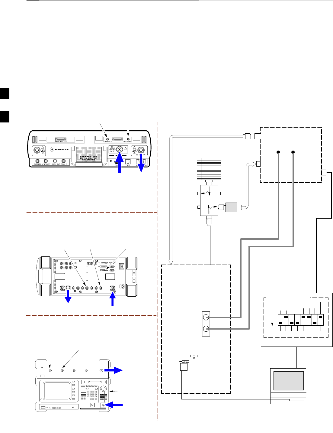
Test Equipment Set–up – continued
DRAFT
SCt4812ET BTS Optimization/ATP — CDMA LMF Apr 2001
3-48
Setup for Optimization/ATP
Figure 3-11 and Figure 3-12 show the test set connections for
optimization/ATP tests.
Motorola CyberTest
Hewlett–Packard Model HP 8935
DUPLEX OUT
TEST SETS Optimization/ATP SET UP
RF
IN/OUT
SYNC MONITOR
EVEN SEC TICK
PULSE REFERENCE
FROM CSM BOARD
FREQ MONITOR
19.6608 MHZ CLOCK
REFERENCE FROM
CSM BOARD
RF IN/OUT
HP–IB
TO GPIB
BOX
Advantest Model R3465
INPUT
50–OHM
GPIB CONNECTS
TO BACK OF UNIT
NOTE: The Directional Coupler is not used
with the Cybertest Test Set. The TX cable is
connected directly to the Cybertest Test set.
RF OUT
RX ANTENNA
PORT OR RFDS
RX ANTENNA
DIRECTIONAL
COUPLER
TX ANTENNA
PORT OR RFDS
RX ANTENNA
DIRECTIONAL
COUPLER
RS232–GPIB
INTERFACE BOX
INTERNAL PCMCIA
ETHERNET CARD
GPIB
CABLE
UNIVERSAL TWISTED
PAIR (UTP) CABLE
(RJ45 CONNECTORS)
RS232 NULL
MODEM
CABLE
S MODE
DATA FORMAT
BAUD RATE
GPIB ADRS G MODE
ON
BTS
TX
TEST
CABLE
CDMA
LMF
DIPSWITCH SETTINGS*
10BASET/
10BASE2
CONVERTER
LAN
B
LAN
A
RX
TEST
CABLE
COMMUNICATIONS
TEST SET
IEEE 488
GPIB BUS
IN
TEST SET
INPUT/
OUTPUT
PORTS
OUT
NOTE: IF BTS RX/TX SIGNALS ARE
DUPLEXED (4800E): BOTH THE TX AND RX
TEST CABLES CONNECT TO THE DUPLEXED
ANTENNA GROUP.
100–WATT (MIN)
NON–RADIATING
RF LOAD
2O DB PAD
FOR 1.9 GHZ
DIRECTIONAL
COUPLER
(30 DB)
EVEN
SECOND/SYNC
IN (BNC “T”
WITH 50 OHM
TERMINATOR)
CDMA
TIMEBASE
IN
FREQ
MONITOR
SYNC
MONITOR
CSM
FW00096
Figure 3-11: Optimization/ATP Test Setup Calibration (CyberTest, HP 8935 and Advantest)
SYNC MONITOR
EVEN SEC TICK
PULSE REFERENCE
FROM CSM BOARD
FREQ MONITOR
19.6608 MHZ CLOCK
REFERENCE FROM
CSM BOARD
SYNC MONITOR
EVEN SEC TICK
PULSE REFERENCE
FROM CSM BOARD
FREQ MONITOR
19.6608 MHZ CLOCK
REFERENCE FROM
CSM BOARD
RF
OUT
* BLACK PORTION OF THE
DIAGRAM REPRESENTS THE
RAISED PART OF THE
SWITCH
3
Test Equipment Set–up – continued
Apr 2001 3-49
SCt4812ET BTS Optimization/ATP — CDMA LMF
DRAFT
RF OUT
ONLY
Hewlett–Packard Model HP 8921A W/PCS Interface
(for 1700 and 1900 MHz)
HP PCS
INTERFACE*
GPIB
CONNECTS
TO BACK OF
UNITS
SYNC MONITOR
EVEN SEC TICK
PULSE REFERENCE
FROM CSM BOARD
FREQ MONITOR
19.6608 MHZ CLOCK
REFERENCE FROM
CSM BOARD
TEST SETS Optimization/ATP SET UP
RX ANTENNA
PORT OR RFDS
RX ANTENNA
DIRECTIONAL
COUPLER
TX ANTENNA
PORT OR RFDS
RX ANTENNA
DIRECTIONAL
COUPLER
RS232–GPIB
INTERFACE BOX
INTERNAL PCMCIA
ETHERNET CARD
GPIB
CABLE
UNIVERSAL TWISTED
PAIR (UTP) CABLE
(RJ45 CONNECTORS)
RS232 NULL
MODEM
CABLE
S MODE
DATA FORMAT
BAUD RATE
GPIB ADRS G MODE
ON
BTS
TX
TEST
CABLE
CDMA
LMF
DIPSWITCH SETTINGS*
10BASET/
10BASE2
CONVERTER
LAN
B
LAN
A
RX
TEST
CABLE
COMMUNICATIONS
TEST SET
IEEE 488
GPIB BUS
IN
TEST SET
INPUT/
OUTPUT
PORTS
OUT
NOTE: IF BTS RX/TX SIGNALS ARE
DUPLEXED (4800E): BOTH THE TX AND RX
TEST CABLES CONNECT TO THE DUPLEXED
ANTENNA GROUP.
100–WATT (MIN)
NON–RADIATING
RF LOAD
2O DB PAD
FOR 1.9 GHZ
EVEN
SECOND/SYNC
IN (BNC “T”
WITH 50 OHM
TERMINATOR)
CDMA
TIMEBASE
IN
FREQ
MONITOR
SYNC
MONITOR
CSM
RF
IN/OUT
Figure 3-12: Optimization/ATP Test Setup HP 8921A
REF FW00097
GPIB
CONNECTS
TO BACK OF
UNIT
SYNC MONITOR
EVEN SEC TICK
PULSE REFERENCE
FROM CSM BOARD
FREQ MONITOR
19.6608 MHZ CLOCK
REFERENCE FROM
CSM BOARD
Hewlett–Packard Model HP 8921A
(for 800 MHz)
* FOR 1700 AND
1900 MHZ ONLY
DIRECTIONAL
COUPLER
(30 DB)
RF
IN/OUT
RF OUT
ONLY
* BLACK PORTION OF THE
DIAGRAM REPRESENTS THE
RAISED PART OF THE
SWITCH
3
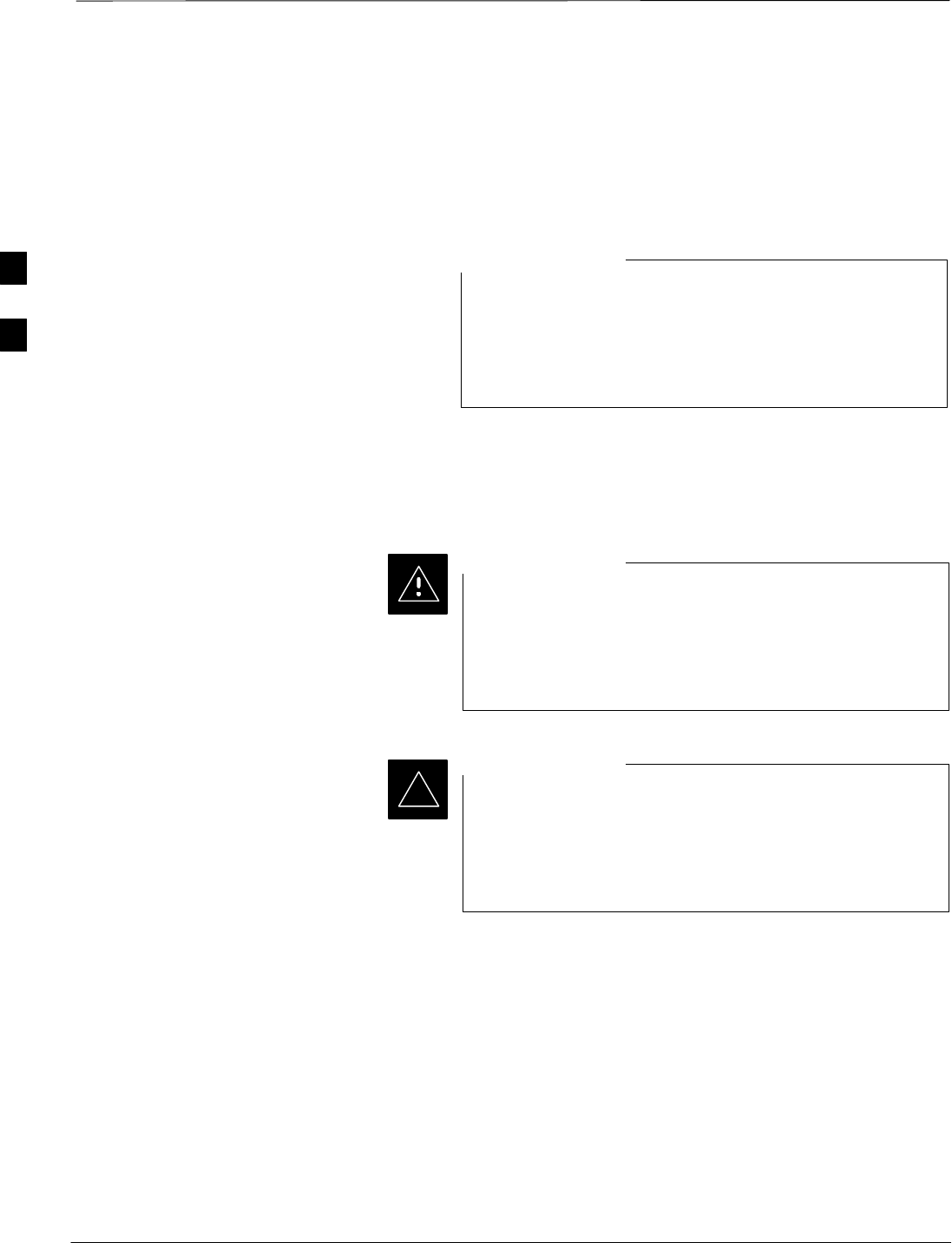
Test Set Calibration
DRAFT
SCt4812ET BTS Optimization/ATP — CDMA LMF Apr 2001
3-50
Background
Proper test equipment setup ensures that the test equipment and
associated test cables do not introduce measurement errors, and that
measurements are correct.
If the test set being used to interface with the BTS has been
calibrated and maintained as a set, this procedure does not
need to be performed. (Test Set includes LMF terminal,
communications test set, additional test equipment,
associated test cables, and adapters.)
NOTE
This procedure must be performed prior to beginning the optimization.
Verify all test equipment (including all associated test cables and
adapters actually used to interface all test equipment and the BTS) has
been calibrated and maintained as a set.
If any piece of test equipment, test cable, or RF adapter,
that makes up the calibrated test equipment set, has been
replaced, re-calibration must be performed. Failure to do so
can introduce measurement errors, resulting in incorrect
measurements and degradation to system performance.
CAUTION
Calibration of the communications test set (or equivalent
test equipment) must be performed at the site before
calibrating the overall test set. Calibrate the test equipment
after it has been allowed to warm–up and stabilize for a
minimum of 60 minutes.
IMPORTANT
*
Purpose
These procedures access the CDMA LMF automated calibration routine
used to determine the path losses of the supported communications
analyzer, power meter, associated test cables, and (if used) antenna
switch that make up the overall calibrated test set. After calibration, the
gain/loss offset values are stored in a test measurement offset file on the
CDMA LMF.
3

Test Set Calibration – continued
DRAFT
Apr 2001 3-51
SCt4812ET BTS Optimization/ATP — CDMA LMF
Selecting Test Equipment
Use LMF Options from the Options menu list to select test equipment
automatically (using the autodetect feature) or manually.
Prerequisites
A Serial Connection and a Network Connection tab are provided for
test equipment selection. The Serial Connection tab is used when the
test equipment items are connected directly to the CDMA LMF
computer via a GPIB box (normal setup). The Network Connection tab
is used when the test equipment is to be connected remotely via a
network connection.
Ensure the following has been completed before selecting test
equipment:
STest equipment is correctly connected and turned on.
SCDMA LMF computer serial port and test equipment are connected to
the GPIB box.
Manually Selecting Test
Equipment in a Serial
Connection Tab
Test equipment can be manually specified before, or after, the test
equipment is connected. CDMA LMF does not check to see if the test
equipment is actually detected for manual specification.
Table 3-22: Selecting Test Equipment Manually in a Serial Connection Tab
Step Action
1From the Options menu, select LMF Options. The LMF Options window appears.
2Click on the Serial Connection tab (if not in the forefront).
3Select the correct serial port in the COMM Port pick list (normally COM1).
4Click on the Manual Specification button (if not enabled).
5Click on the check box corresponding to the test item(s) to be used.
6Type the GPIB address in the corresponding GPIB address box. Recommended Addresses
13=Power Meter
18=CDMA Analyzer
7Click on Apply. (The button will darken until the selection has been committed.)
NOTE
With manual selection, CDMA LMF does not detect the test equipment to see if it is connected and
communicating with CDMA LMF.
8Click on Dismiss to close the test equipment window.
3

Test Set Calibration – continued
DRAFT
SCt4812ET BTS Optimization/ATP — CDMA LMF Apr 2001
3-52
Automatically Selecting Test
Equipment in a Serial
Connection Tab When using the auto-detection feature to select test equipment, the
CDMA LMF examines which test equipment items are actually
communicating with CDMA LMF. Follow the procedure in Table 3-23
to use the auto-detect feature.
Table 3-23: Selecting Test Equipment Using Auto-Detect
Step Action
1From the Options menu, select LMF Options. The LMF Options window appears.
2Click on the Serial Connection tab (if not in the forefront).
3Select the correct serial port in the COMM Port pick list (normally COM1).
4Click on Auto–Detection (if not enabled).
5Type in the GPIB addresses in the box labeled GPIB address to search (if not already displayed).
NOTE
When both a power meter and analyzer are selected, the first item listed in the GPIB addresses to
search box will be used for RF power measurements (i.e., TX calibration). The address for a power
meter is normally 13 and the address for a CDMA analyzer is normally 18. If 13,18 is included in the
GPIB addresses to search box, the power meter (13) will be used for RF power measurements. If the
test equipment items are manually selected the CDMA analyzer is used only if a power meter is not
selected.
6 Click Apply. The button will darken until the selection has been committed. A check mark will
appear in the Manual Configuration section for detected test equipment items.
7 Click Dismiss to close the LMF Options window.
3

Test Set Calibration – continued
DRAFT
Apr 2001 3-53
SCt4812ET BTS Optimization/ATP — CDMA LMF
Calibrating Test Equipment
The calibrate test equipment function zeros the power measurement level
of the test equipment item that is to be used for TX calibration and audit.
If both a power meter and an analyzer are connected, only the power
meter is zeroed.
Calibrate Test Equipment from the Util menu list is used to calibrate
test equipment item before being used for testing. The test equipment
must be selected before beginning calibration. Follow the procedure in
Table 3-24 to calibrate the test equipment.
Table 3-24: Test Equipment Calibration
Step Action
1From the Util menu, select Calibrate Test Equipment. A Directions window is displayed. Follow
the instructions provided.
2Follow the direction provided.
3Click on Continue to close the Directions window. A status window is displayed.
4Click on OK to close the status report window.
Calibrating Cables
The cable calibration function is used to measure the loss (in dB) for the
TX and RX cables that are to be used for testing. A CDMA analyzer is
used to measure the loss of each cable configuration (TX cable
configuration and RX cable configuration). The cable calibration
consists of the following steps.
SMeasure the loss of a short cable. This is done to compensate for any
measurement error of the analyzer. The short cable, which is used only
for the calibration process, is used in series with both the TX and RX
cable configuration when they are measured. The measured loss of the
short cable is deducted from the measured loss of the TX and RX
cable configuration to determine the actual loss of the TX and RX
cable configurations. This deduction is done so any error in the
analyzer measurement will be adjusted out of both the TX and RX
measurements.
SThe short cable plus the RX cable configuration loss is measured. The
RX cable configuration normally consists only of a coax cable with
type–N connectors that is long enough to reach from the BTS RX port
the test equipment.
SThe short cable plus the TX cable configuration loss is measured. The
TX cable configuration normally consists of two coax cables with
type–N connectors and a directional coupler, a load, and an additional
attenuator if required by the BTS type. The total loss of the path loss
of the TX cable configuration must be as required for the BTS
(normally 30 or 50 dB). The Motorola Cybertest analyzer is different
in that the required attenuation/load is built into the test set so the TX
cable configuration consists only of the required length coax cable.
3

Test Set Calibration – continued
DRAFT
SCt4812ET BTS Optimization/ATP — CDMA LMF Apr 2001
3-54
Calibrating Cables with a
CDMA Analyzer
The Cable Calibration menu item from the Util menu list is used to
calibrate both TX and RX test cables for use with CDMA LMF.
LMF cable calibration cannot be accomplished with an
HP8921A analyzer for 1.9 MHz. A different analyzer type
or the signal generator and spectrum analyzer method must
be used (refer to Table 3-26 and Table 3-27). Cable
calibration values must be manually entered if the signal
generator and spectrum analyzer method is used. For the
HP8921A, refer to Appendix F.
NOTE
The test equipment must be selected before this procedure can be started.
Follow the procedure in Table 3-25 to calibrate the cables. Figure 3-8
illustrates the cable calibration test equipment setup.
Table 3-25: Cable Calibration
Step Action
1From the Util menu, select Cable Calibration. A Cable Calibration window is displayed.
2Enter a channel number(s) in the Channels box. Multiple channels numbers must be separated with a
comma, no space (i.e., 200,800). When two or more channels numbers are entered, the cables will be
calibrated for each channel. Interpolation will be accomplished for other channels as required for TX
calibration.
3 Select TX and RX CABLE CAL, TX CABLE CAL or RX CABLE CAL in the Cable Calibration
picklist.
4 Click OK. Follow the directions displayed for each step. A status report window will be displayed
with the results of the cable calibration.
3
Test Set Calibration – continued
DRAFT
Apr 2001 3-55
SCt4812ET BTS Optimization/ATP — CDMA LMF
Calibrating TX Cables Using a
Signal Generator and
Spectrum Analyzer
Follow the procedure in Table 3-26 to calibrate the TX cables using the
signal generator and spectrum analyzer. Refer to Figure 3-13 for a
diagram of the signal generator and spectrum analyzer.
Table 3-26: Calibrating TX Cables Using Signal Generator and Spectrum Analyzer
Step Action
1Connect a short test cable between the spectrum analyzer and the signal generator.
2Set signal generator to 0 dBm at the customer frequency of 1840–1870 MHz band for Korea PCS and
1930–1990 MHz band for North American PCS.
3Use spectrum analyzer to measure signal generator output (see Figure 3-13, “A”) and record the value.
4Connect the spectrum analyzer’s short cable to point “B”, as shown in the lower portion of the
diagram, to measure cable output at customer frequency (1840–1870 MHz for Korea PCS and
1930–1990 MHz for North American PCS) and record the value at point “B”.
5Calibration factor = A – B Example: Cal = –1 dBm – (–53.5 dBm) = 52.5 dB
NOTE
The short cable is used for calibration only. It is not part of the final test setup. After calibration is
completed, do not re-arrange any cables. Use the equipment setup, as is, to ensure test procedures use
the correct calibration factor.
Figure 3-13: Calibrating Test Equipment Setup for TX Cable Calibration
(Using Signal Generator and Spectrum Analyzer)
50 OHM
TERMINATION
30 DB
DIRECTIONAL
COUPLER
Spectrum
Analyzer
Signal
Generator
A
Spectrum
Analyzer
40W NON–RADIATING
RF LOAD
B
SHORT TEST CABLE
Signal
Generator
THIS WILL BE THE CONNECTION TO THE
POWER METER DURING TX CALIBRATION
AND TO THE CDMA ANALYZER DURING TX
ATP TESTS.
SHORT
TEST
CABLE THIS WILL BE THE CONNECTION
TO THE TX PORTS DURING TX
CALIBRATION AND TO THE TX/RX
PORTS DURING ATP TESTS.
SECOND RF
TEST CABLE.
ONE 20DB 20 W IN
LINE ATTENUATOR
FW00293
3
Test Set Calibration – continued
DRAFT
SCt4812ET BTS Optimization/ATP — CDMA LMF Apr 2001
3-56
Calibrating RX Cables Using a
Signal Generator and
Spectrum Analyzer Follow the procedure in Table 3-27 to calibrate the RX cables using the
signal generator and spectrum analyzer. Refer to Figure 3-14, if required.
Table 3-27: Calibrating RX Cables Using a Signal Generator and Spectrum Analyzer
Step Action
1Connect a short test cable to the spectrum analyzer and connect the other end to the Signal Generator.
2Set signal generator to –10 dBm at the customer’s RX frequency of 1750–1780 MHz for Korean PCS
and 1850–1910 MHz band for North American PCS.
3Use spectrum analyzer to measure signal generator output (see Figure 3-14, “A”) and record the value
for “A”.
4Connect the test setup, as shown in the lower portion of the diagram, to measure the output at the
customer’s RX frequency in the 1850–1910 MHz band. Record the value at point ‘‘B”.
5Calibration factor = A – B
Example: Cal = –12 dBm – (–14 dBm) = 2 dB
NOTE
The short test cable is used for test equipment setup calibration only. It is not be part of the final test
setup. After calibration is completed, do not re-arrange any cables. Use the equipment setup, as is, to
ensure test procedures use the correct calibration factor.
Figure 3-14: Calibrating Test Equipment Setup for RX ATP Test
(Using Signal Generator and Spectrum Analyzer)
Spectrum
Analyzer
Signal
Generator
A
B
Spectrum
Analyzer
SHORT
TEST
CABLE
SHORT TEST
CABLE
CONNECTION TO THE OUTPUT
PORT DURING RX MEASUREMENTS
Signal
Generator
BULLET
CONNECTOR
LONG
CABLE 2
CONNECTION TO THE RX PORTS
DURING RX MEASUREMENTS. FW00294
3

Test Set Calibration – continued
DRAFT
Apr 2001 3-57
SCt4812ET BTS Optimization/ATP — CDMA LMF
Setting Cable Loss Values Cable loss values for the TX and RX test cable configurations are
normally set by accomplishing cable calibration with use of the
applicable test equipment. The resulting values are stored in the cable
loss files. The cable loss values can also be set/changed manually.
Prerequisites
SLogged into the BTS
Table 3-28: Setting Cable Loss Values
Step Action
1Click on the Util menu.
2 Select Edit >Cable Loss > TX or RX. A data entry pop–up window will appear.
3Click on the Add Row button to add a new channel number. Then click in the Channel # and Loss
(dBm) columns and enter the desired values.
4To edit existing values click in the data box to be changed and change the value.
5To delete a row, click on the row and then click on the Delete Row button.
6Click on the Save button to save displayed values.
7Click on the Dismiss button to exit the window. Values that were entered/changed after the Save
button was used will not be saved.
NOTE
SIf cable loss values exist for two different channels the LMF will interpolate for all other channels.
SEntered values will be used by the LMF as soon as they are saved. You do not have to logout and
login.
3

Test Set Calibration – continued
DRAFT
SCt4812ET BTS Optimization/ATP — CDMA LMF Apr 2001
3-58
Setting TX Coupler Loss Value If an in–service TX coupler is installed the coupler loss (e.g., 30 dB)
must be manually entered so it will be included in the LMF TX
calibration and audit calculations.
Prerequisites
SLogged into the BTS
Table 3-29: Setting TX Coupler Loss Values
Step Action
1Click on the Util menu.
2 Select Edit >TX Coupler Loss. A data entry pop–up window will appear.
3Click in the Loss (dBm) column for each carrier that has a coupler and enter the appropriate value.
4To edit existing values click in the data box to be changed and change the value.
5Click on the Save button to save displayed values.
6Click on the Dismiss button to exit the window. Values that were entered/changed after the Save
button was used will not be saved.
NOTE
SThe In–Service Calibration check box in the Options>LMF Options>BTS Options tab must
checked before entered TX coupler loss values will be used by the TX calibration and audit
functions.
SEntered values will be used by the LMF as soon as they are saved. You do not have to logout and
login.
3

Bay Level Offset Calibration
Apr 2001 3-59
SCt4812ET BTS Optimization/ATP — CDMA LMF
DRAFT
Introduction
Calibration compensates for normal equipment variations within the
BTS and assures maximum measurement accuracy.
RF Path Bay Level Offset
Calibration
Calibration identifies the accumulated gain in every transmit path
(BBX2 slot) at the BTS site and stores that value in the CAL file. The
BLOs are subsequently downloaded to each BBX2.
Each receive path starts at a BTS RX antenna port and terminates at a
backplane BBX2 slot. Each transmit path starts at a BBX2 backplane
slot, travels through the LPA, and terminates at a BTS TX antenna port.
Calibration identifies the accumulated gain in every transmit path
(BBX2 slot) at the BTS site and stores that value in the CAL file. Each
transmit path starts at a C–CCP shelf backplane BBX2 slot, travels
through the LPA, and ends at a BTS TX antenna port. When the TX path
calibration is performed, the RX path BLO will automatically be set to
the default value.
When to Calibrate BLOs Calibration of BLOs is required after initial BTS installation.
The BLO data of an operational BTS site must be re-calibrated once
each year. Motorola recommends re-calibrating the BLO data for all
associated RF paths after replacing any of the following components or
associated interconnecting RF cabling:
SBBX2 board
SC–CCP shelf
SCIO card
SCIO to LPA backplane RF cable
SLPA backplane
SLPA
STX filter / TX filter combiner
STX thru-port cable to the top of frame
3
Bay Level Offset Calibration – continued
DRAFT
SCt4812ET BTS Optimization/ATP — CDMA LMF Apr 2001
3-60
TX Path Calibration
The TX Path Calibration assures correct site installation, cabling, and the
first order functionality of all installed equipment. The proper function
of each RF path is verified during calibration. The external test
equipment is used to validate/calibrate the TX paths of the BTS.
Before installing any test equipment directly to any TX
OUT connector you must first verify that there are no
CDMA channels keyed. Have the OMC–R place the sector
assigned to the LPA under test OOS. Failure to do so can
result in serious personal injury and/or equipment damage.
WARNING
Always wear a conductive, high impedance wrist strap
while handling any circuit card/module. If this is not done,
there is a high probability that the card/module could be
damaged by ESD.
CAUTION
At new site installations, to facilitate the complete test of
each CCP shelf (if the shelf is not already fully populated
with BBX2 boards), move BBX2 boards from shelves
currently not under test and install them into the empty
BBX2 slots of the shelf currently being tested to insure that
all BBX2 TX paths are tested.
–This procedure can be bypassed on operational sites
that are due for periodic optimization.
–Prior to testing, view the CDF file to verify the
correct BBX2 slots are equipped. Edit the file as
required to include BBX2 slots not currently
equipped (per Systems Engineering documentation).
IMPORTANT
*
3
Bay Level Offset Calibration – continued
Apr 2001 3-61
SCt4812ET BTS Optimization/ATP — CDMA LMF
DRAFT
BLO Calibration Data File
During the calibration process, the LMF creates a calibration (BLO) data
file. After calibration has been completed, this offset data must be
downloaded to the BBX2s using the Download BLO function. An
explanation of the file is shown below.
Due to the size of the file, Motorola recommends that you
print out a hard copy of a bts.cal file and refer to it for the
following descriptions.
NOTE
The CAL file is subdivided into sections organized on a per slot basis (a
slot Block).
Slot 1 contains the calibration data for the 12 BBX2 slots. Slot 20
contains the calibration data for the redundant BBX2 (see Table 3-31).
Each BBX2 slot header block contains:
SA creation Date and Time – broken down into separate parameters of
createMonth, createDay, createYear, createHour, and createMin.
SThe number of calibration entries – fixed at 720 entries corresponding
to 360 calibration points of the CAL file including the slot header and
actual calibration data.
SThe calibration data for a BBX2 is organized as a large flat array. The
array is organized by branch, BBX2 slot, and calibration point.
–The first breakdown of the array indicates which branch the
contained calibration points are for. The array covers transmit, main
receive and diversity receive offsets as follows:
Table 3-30: BLO BTS.cal file Array Branch Assignments
Range Assignment
C[1]–C[240] Transmit
C[241]–C[480] Receive
C[481]–C[720] Diversity Receive
3

Bay Level Offset Calibration – continued
DRAFT
SCt4812ET BTS Optimization/ATP — CDMA LMF Apr 2001
3-62
–The second breakdown of the array is per sector. Three sectors are
allowed.
Table 3-31: BTS.cal File Array (Per Sector)
BBX2 Sectorization TX RX RX Diversity
Slot[1] (Primary BBX2s 1 through 12)
1 (Omni) 3–Sector, C[1]–C[20] C[241]–C[260] C[481]–C[500]
23–Sector,
1st C[21]–C[40] C[261]–C[280] C[501]–C[520]
36 Sector, Carrier C[41]–C[60] C[281]–C[300] C[521]–C[540]
41st
Carrier 3–Sector, C[61]–C[80] C[301]–C[320] C[541]–C[560]
5Carrier 3–Sector,
3rd C[81]–C[100] C[321]–C[340] C[561]–C[580]
6Carrier C[101]–C[120] C[341]–C[360] C[581]–C[600]
73–Sector, C[121]–C[140] C[361]–C[380] C[601]–C[620]
83–Sector,
2nd C[141]–C[160] C[381]–C[400] C[621]–C[640]
96 Sector, Carrier C[161]–C[180] C[401]–C[420] C[641]–C[660]
10 2nd
Carrier 3–Sector, C[181]–C[200] C[421]–C[440] C[661]–C[680]
11 Carrier 3–Sector,
4th C[201]–C[220] C[441]–C[460] C[681]–C[700]
12 Carrier C[221]–C[240] C[461]–C[480] C[701]–C[720]
Slot[20] (Redundant BBX2–13)
1 (Omni) 3–Sector, C[1]–C[20] C[241]–C[260] C[481]–C[500]
23–Sector,
1st C[21]–C[40] C[261]–C[280] C[501]–C[520]
36 Sector, Carrier C[41]–C[60] C[281]–C[300] C[521]–C[540]
41st
Carrier 3–Sector, C[61]–C[80] C[301]–C[320] C[541]–C[560]
5Carrier 3–Sector,
3rd C[81]–C[100] C[321]–C[340] C[561]–C[580]
6Carrier C[101]–C[120] C[341]–C[360] C[581]–C[600]
73–Sector, C[121]–C[140] C[361]–C[380] C[601]–C[620]
83–Sector,
2nd C[141]–C[160] C[381]–C[400] C[621]–C[640]
96 Sector, Carrier C[161]–C[180] C[401]–C[420] C[641]–C[660]
10 2nd
Carrier 3–Sector, C[181]–C[200] C[421]–C[440] C[661]–C[680]
11 Carrier 3–Sector,
4th C[201]–C[220] C[441]–C[460] C[681]–C[700]
12 Carrier C[221]–C[240] C[461]–C[480] C[701]–C[720]
SRefer to the hard copy of the file. As you can see, 10 calibration
points per sector are supported for each branch. Two entries are
required for each calibration point.
SThe first value (all odd entries) refer to the CDMA channel
(frequency) the BLO is measured at. The second value (all even
entries) is the power set level. The valid range for PwrLvlAdj is from
2500 to 27500 (2500 corresponds to –125 dBm and 27500
corresponds to +125 dBm).
3

Bay Level Offset Calibration – continued
Apr 2001 3-63
SCt4812ET BTS Optimization/ATP — CDMA LMF
DRAFT
SThe 20 calibration entries for each slot/branch combination must be
stored in order of increasing frequency. If less than 10 points
(frequencies) are calibrated, the largest frequency that is calibrated is
repeated to fill out the 10 points.
Example:
C[1]=384, odd cal entry = 1 ‘‘calibration point”
C[2]=19102, even cal entry
C[3]=777,
C[4]=19086,
.
.
C[19]=777,
C[20]=19086, (since only two cal points were calibrated this
would be repeated for the next 8 points)
SWhen the BBX2 is loaded with BLO data, the cal file data for the
BBX2 is downloaded to the device in the order it is stored in the CAL
file. TxCal data is sent first, C[1] – C[60]. BBX2 slot 1’s 10
calibration points are sent (C[1] – C[20]), followed by BBX2 slot 2’s
10 calibration points (C[21] – C[40]), etc. The RxCal data is sent next,
followed by the RxDCal data.
STemperature compensation data is also stored in the cal file for each
slot.
Test Equipment Setup:
RF Path Calibration
Follow the steps outlined in Table 3-32 to set up test equipment.
Table 3-32: Test Equipment Setup (RF Path Calibration)
Step Action
NOTE
Verify the GPIB is properly connected and turned on.
! CAUTION
To prevent damage to the test equipment, all transmit (TX) test connections must be via the 30 dB
directional coupler for 800 MHz or via a 30 dB coupler with a 20 dB in–line attenuator for 1900 MHz.
1Connect the LMF computer terminal to the BTS LAN A connector on the BTS (if you have not
already done so). Refer to the procedure in Table 3-6.
SIf required, calibrate the test equipment per the procedure in Table 3-24.
SConnect the test equipment as shown in Figure 3-9 and Figure 3-10.
3

Bay Level Offset Calibration – continued
DRAFT
SCt4812ET BTS Optimization/ATP — CDMA LMF Apr 2001
3-64
Transmit (TX) Path Calibration
The assigned channel frequency and power level (as measured at the top
of the frame) for transmit calibration is derived from the site CDF file.
For each BBX2, the channel frequency is specified in the ChannelList
CDF file parameter and the power is specified in the SIFPilotPwr
CDF file parameter for the sector associated with the BBX2 (located
under the ParentSECTOR field of the ParentCARRIER CDF file
parameter).
The calibration procedure attempts to adjust the power to within +0.5 dB
of the desired power. The calibration will pass if the error is less than
+1.5 dB.
The TX Bay Level Offset at sites WITHOUT the directional coupler
option, is approximately 42.0 dB ±3.0 dB.
SAt sites WITHOUT RFDS option, BLO is approximately
42.0 dB ±4.0 dB. A typical example would be TX output power
measured at BTS (36.0 dBm) minus the BBX2 TX output level
(approximately –6.0 dBm) would equate to 42 dB BLO.
The TX Bay Level Offset at sites WITH the directional coupler option,
is approximately 41.4 dB ±3.0 dB. TX BLO = Frame Power Output
minus BBX2 output level.
SExample: TX output power measured at RFDS TX coupler
(39.4 dBm) minus the BBX TX output level (approximately
–2.0 dBm) and RFDS directional coupler/cable (approximately
–0.6 dBm) would equate to 41.4 dB BLO.
The LMF Tests menu list items, TX Calibration and All Cal/Audit,
perform the TX BLO Calibration test for a XCVR(s). The All Cal/Audit
menu item performs TX calibration, downloads BLO, and performs TX
audit if the TX calibration passes. All measurements are made through
the appropriate TX output connector using the calibrated TX cable setup.
Prerequisites
Before running this test, ensure that the following have been done:
SCSM–1,GLIs, MCCs, and BBX2s have correct code load and data
load.
SPrimary CSM and MGLI are INS.
SAll BBX2s are OOS_RAM.
STest equipment and test cables are calibrated and connected for TX
BLO calibration.
SLMF is logged into the BTS.
Connect the test equipment as shown in Figure 3-9 and Figure 3-10 and
follow the procedure in Table 3-33 to perform the TX calibration test.
3
Bay Level Offset Calibration – continued
Apr 2001 3-65
SCt4812ET BTS Optimization/ATP — CDMA LMF
DRAFT
Before installing any test equipment directly to any TX
OUT connector, first verify there are no CDMA BBX2
channels keyed. Failure to do so can result in serious
personal injury and/or equipment damage.
WARNING
Verify all BBX2 boards removed and repositioned have
been returned to their assigned shelves/slots. Any BBX2
boards moved since they were downloaded will have to be
downloaded again.
IMPORTANT
*
Table 3-33: BTS TX Path Calibration
Step Action
1Select the BBX2(s) to be calibrated.
2From the Tests menu, select TX Calibration or All Cal/Audit.
3Select the appropriate carrier(s) displayed in the Channels/Carrier pick list.
Press and hold the <Shift> or <Ctrl> key to select multiple items.
4Type the appropriate channel number in the Carrier n Channels box.
5Click on OK.
6Follow the cable connection directions as they are displayed.
The test results will be displayed in the status report window.
7Click on Save Results or Dismiss to close the status report window.
Exception Handling
In the event of a failure, the calibration procedure displays a FAIL
message in the status report window and provides information in the
Description field.
Recheck the test setup and connection and re–run the test. If the tests fail
again, note specifics about the failure, and refer to Chapter 6,
Troubleshooting.
Download BLO Procedure
After a successful TX path calibration, download the BLO calibration
file data to the BBX2s. BLO data is extracted from the CAL file for the
BTS and downloaded to the selected BBX2 devices.
3
Bay Level Offset Calibration – continued
DRAFT
SCt4812ET BTS Optimization/ATP — CDMA LMF Apr 2001
3-66
If a successful All Cal/Audit was completed, this
procedure does not need to be performed, as BLO is
downloaded as part of the All Cal/Audit.
NOTE
Prerequisites
Ensure the following prerequisites have been met before proceeding.
SBBXs being downloaded are OOS–RAM (yellow).
STX calibration successfully completed
Follow the steps in Table 3-34 to download the BLO data to the BBX2s.
Table 3-34: Download BLO
Step Action
1Select the BBX2(s) to be downloaded.
2From the Device menu, select Download BLO.
A status report window displays the result of the download.
NOTE
Selected device(s) do not change color when BLO is downloaded.
3 Click OK to close the status report window.
3
Bay Level Offset Calibration – continued
Apr 2001 3-67
SCt4812ET BTS Optimization/ATP — CDMA LMF
DRAFT
Calibration Audit Introduction
The BLO calibration audit procedure confirms the successful generation
and storage of the BLO calibrations. The calibration audit procedure
measures the path gain or loss of every BBX2 transmit path at the site.
In this test, actual system tolerances are used to determine the success or
failure of a test. The same external test equipment set up is used.
*RF path verification, BLO calibration, and BLO data
download to BBX2s must have been successfully
completed prior to performing the calibration audit.
IMPORTANT
Transmit (TX) Path Audit
Perform the calibration audit of the TX paths of all equipped BBX2
slots, per the steps in Table 3-35.
Before installing any test equipment directly to any TX
OUT connector, first verify there are no CDMA BBX2
channels keyed. Failure to do so can result in serious
personal injury and/or equipment damage.
WARNING
If a successful All Cal/Audit was completed, this
procedure does not need to be performed, as BLO is
downloaded as part of the All Cal/Audit.
NOTE
3

Bay Level Offset Calibration – continued
DRAFT
SCt4812ET BTS Optimization/ATP — CDMA LMF Apr 2001
3-68
TX Audit Test
The Tests menu item, TX Audit, performs the TX BLO Audit test for a
BBX2(s). All measurements are made through the appropriate TX output
connector using the calibrated TX cable setup.
Prerequisites
Before running this test, the following should be done:
SCSM–1,GLI2s, BBX2s have correct code load.
SPrimary CSM and MGLI2 are INS.
SAll BBX2s are OOS_RAM.
STest equipment and test cables are calibrated and connected for TX
BLO calibration.
SLMF is logged into the BTS.
Connect the test equipment as shown in Figure 3-9 and Figure 3-10 and
follow the procedure in Table 3-35 to perform the BTS TX Path Audit
test.
Table 3-35: TX Path Audit
Step Action
1Select the BBX2(s) to be audited. From the Tests menu, select TX Audit.
2Select the appropriate carrier(s) displayed in the Channels/Carrier pick list.
Press and hold the <Shift> or <Ctrl> key to select multiple items.
3Type the appropriate channel number in the Carrier n Channels box.
4Click on OK.
5Follow the cable connection directions as they are displayed.
A status report window displays the test results.
6Click on Save Results or Dismiss to close the status report window.
Exception Handling
In the event of a failure, the calibration procedure displays a FAIL
message in the status report window and provides information in the
Description field.
Recheck the test setup and connection and re–run the test. If the tests fail
again, note specifics about the failure, and refer to Chapter 6,
Troubleshooting.
3
Bay Level Offset Calibration – continued
Apr 2001 3-69
SCt4812ET BTS Optimization/ATP — CDMA LMF
DRAFT
All Cal/Audit Test
The Tests menu item, All Cal/Audit, performs the TX BLO Calibration
and Audit test for a XCVR(s). All measurements are made through the
appropriate TX output connector using the calibrated TX cable setup.
If the TX calibration portion of the test passed, the BLO
data will automatically be downloaded to the BBX2(s)
before the audit portion of the test is run.
NOTE
Prerequisites
Before running this test, the following should be done:
SCSM–1, GLI2s, BBX2s have correct code and data load.
SPrimary CSM and MGLI2 are INS.
SAll BBXs are OOS_RAM.
STest equipment and test cables are calibrated and connected for TX
BLO calibration.
SLMF is logged into the BTS.
Follow the procedures in Table 3-36 to perform the All Cal/Audit test.
Before installing any test equipment directly to any TX
OUT connector, first verify there are no CDMA BBX2
channels keyed. Failure to do so can result in serious
personal injury and/or equipment damage.
WARNING
Table 3-36: All Cal/Audit Test
Step Action
1Select the BBX2(s) to be tested.
From the Tests menu, select All Cal/Audit.
2Select the appropriate carrier(s) displayed in the Channels/Carrier pick list.
Press and hold the <Shift> or <Ctrl> key to select multiple items.
3Type the appropriate channel number in the Carrier n Channels box.
4Click on OK.
5Follow the cable connection directions as they are displayed.
A status report window displays the test results.
6Click on Save Results or Dismiss to close the status report window.
3
Bay Level Offset Calibration – continued
DRAFT
SCt4812ET BTS Optimization/ATP — CDMA LMF Apr 2001
3-70
Create CAL File
The Create Cal File function gets the BLO data from BBXs and
creates/updates the CAL file for the BTS. If a CAL file does not exist a
new one is created. If a CAL file already exists it is updated. After a
BTS has been fully optimized a copy of the CAL file must exist so it can
be transferred to the CBSC. If TX calibration has been successfully
performed for all BBXs and BLO data has been downloaded, a CAL file
will exist. Note the following:
SThe Create Cal File function only applies to selected (highlighted)
BBXs.
Editing the CAL file is not encouraged as this action can
cause interface problems between the BTS and the LMF.
To manually edit the CAL file you must first logout of the
BTS. If you manually edit the CAL file and then use the
Create Cal File function the edited information will be lost.
WARNING
Prerequisites
Before running this test, the following should be done:
SLMF is logged in to the BTS
SBBX2s are OOS_RAM with BLO downloaded
Table 3-37: Create CAL File
Step Action
1Select the applicable BBX2s. The CAL file will only be updated for the selected BBX2s.
2Click on the Device menu.
3Click on the Create Cal File menu item. The status report window is displays the results of the action.
4 Click OK.
3