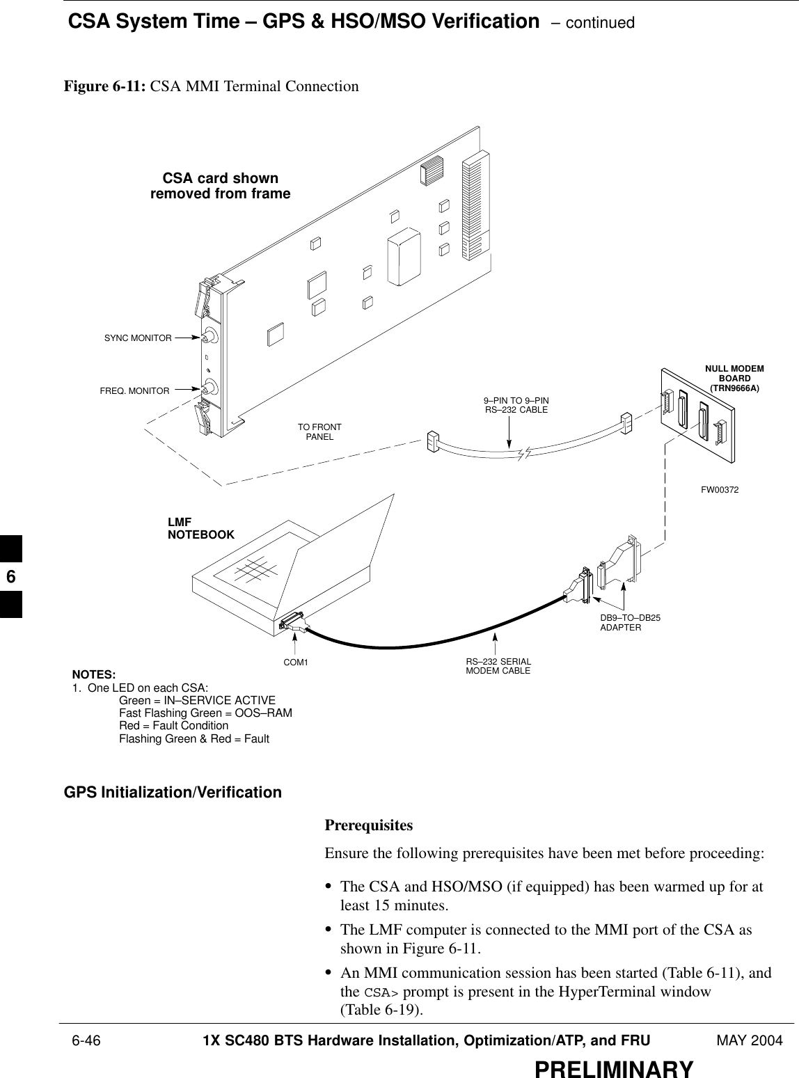
Nokia Solutions and Networks T5EJ1 1X SC480 BTS Microcell Base Station Transmitter User Manual print instructions
Nokia Solutions and Networks 1X SC480 BTS Microcell Base Station Transmitter print instructions
Contents
- 1. User Manual Part 1
- 2. User Manual Part 2
- 3. User Manual Part 3
- 4. User Manual Part 4
User Manual Part 2
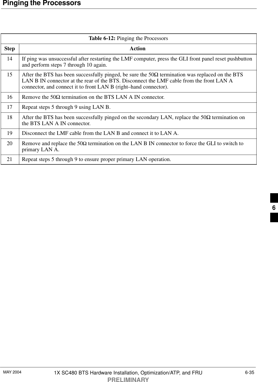
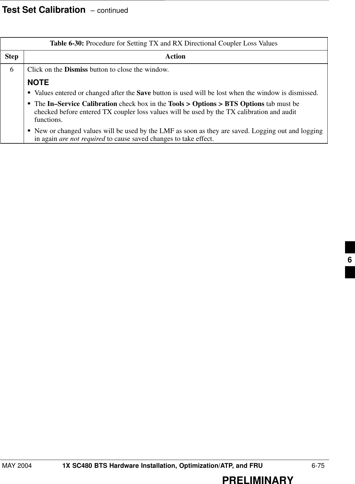
![Bay Level Offset Calibration – continuedMAY 2004 1X SC480 BTS Hardware Installation, Optimization/ATP, and FRU 6-77PRELIMINARYBLO Calibration Data FileDuring the calibration process, the LMF creates a calibration (CAL) datafile where BLO values are stored. After calibration has been completed,these offset values must be downloaded to the BBXs using the LMFBLO download function. A detailed description of the file organizationand content is provided in the following paragraphsNOTE Due to the size of the file, Motorola recommends printing out acopy of a bts–#.cal file and referring to it for the followingdescriptions.SWhen referring to the CAL file print–out it can be seen that there isone BBX slot with 20 “calibration entries” per BBX (sector) for eachbranch. Two calibration entries define a single “calibration point;”therefore there are ten calibration points in each branch for each BBX.– The first entry for a calibration point (all odd entries) identifies theCDMA channel (frequency) where the BLO is measured. Thesecond calibration entry (all even entries) is the power set level(PwrLvlAdj) for that frequency. The valid range for PwrLvlAdj isfrom 2500 to 27500 (2500 corresponds to –125 dBm and 27500corresponds to +125 dBm).– The ten calibration points for each slot–branch combination must bestored in order of increasing frequency. If less than ten points(frequencies) are calibrated, the BLO data for the highest frequencycalibrated is written into the remainder of the ten points for thatslot–branch.Example:C[1]=384 (odd cal entry)C[2]=19102 (even cal entry)C[3]=777 (odd cal entry)C[4]=19086 (even cal entry)C[19]=777 (odd cal entry)C[20]=19086 (even cal entry)...= 1 “calibration point”= 1 “calibration point”= 1 “calibration point”In the example above, BLO was measured at only two frequencies(channels 384 and 777) for CCP2 slot BBX–1 transmit. The BLO datafor the highest frequency measured (channel 777) will be written tothe remaining eight transmit calibration points (defined by entriesC[5] through C[20]) for BBX–1.Slot Block Temperature Compensation – Each BBX slot Block alsohas a temperature compensation data section (TempLevelCal) wherepower level compensation factors for temperature variations are stored.6](https://usermanual.wiki/Nokia-Solutions-and-Networks/T5EJ1.User-Manual-Part-2/User-Guide-430568-Page-93.png)
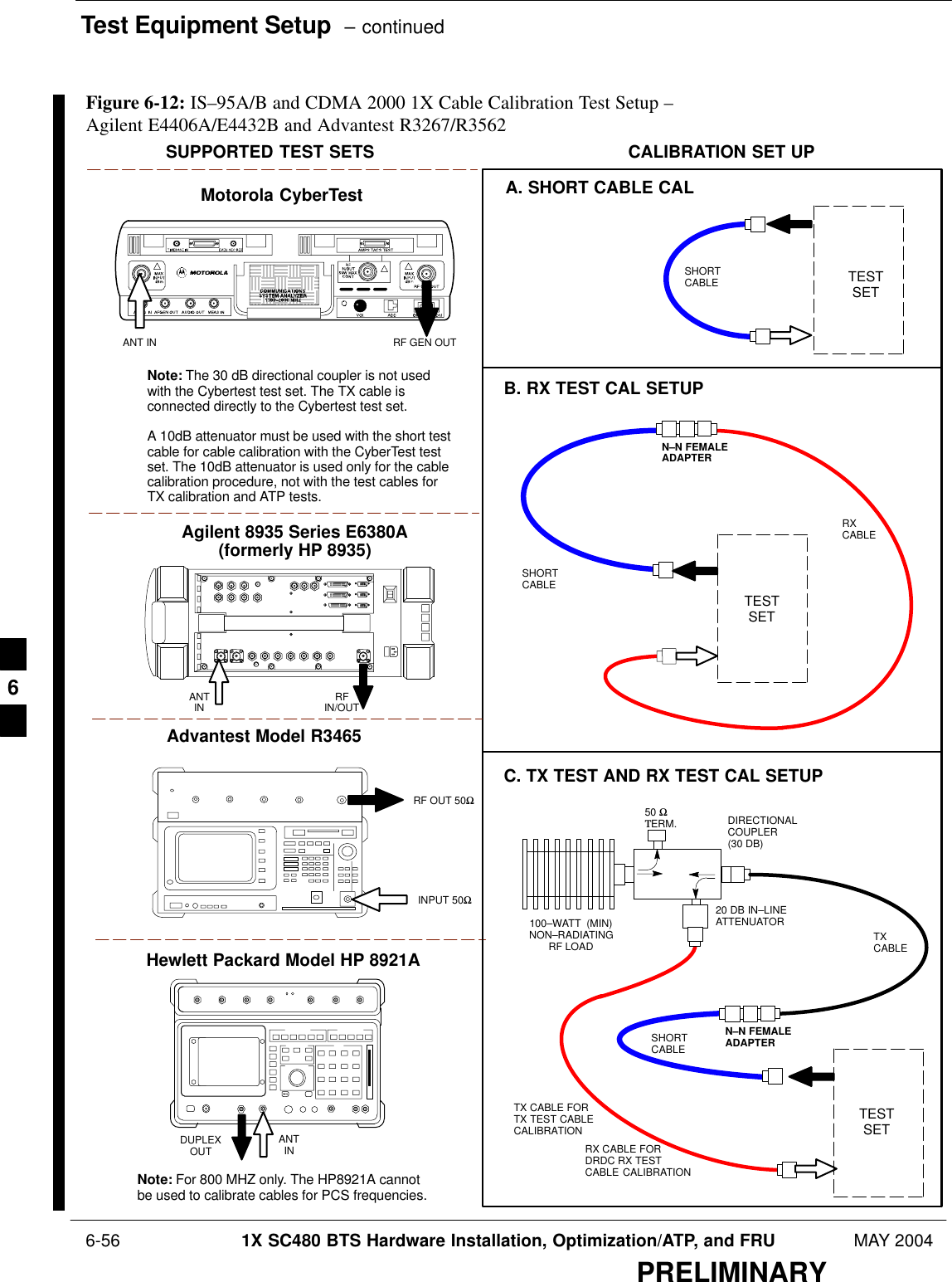
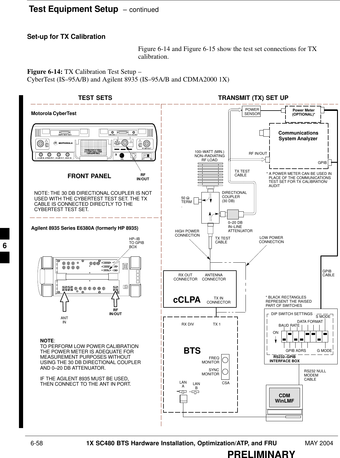
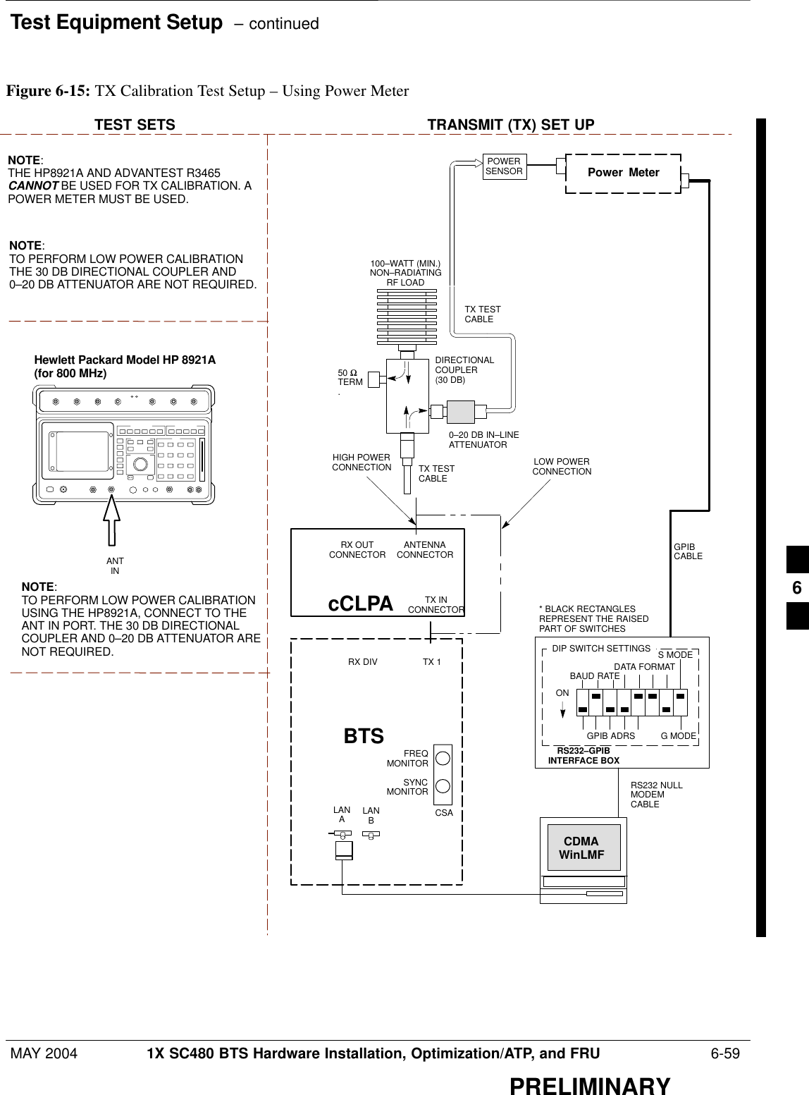
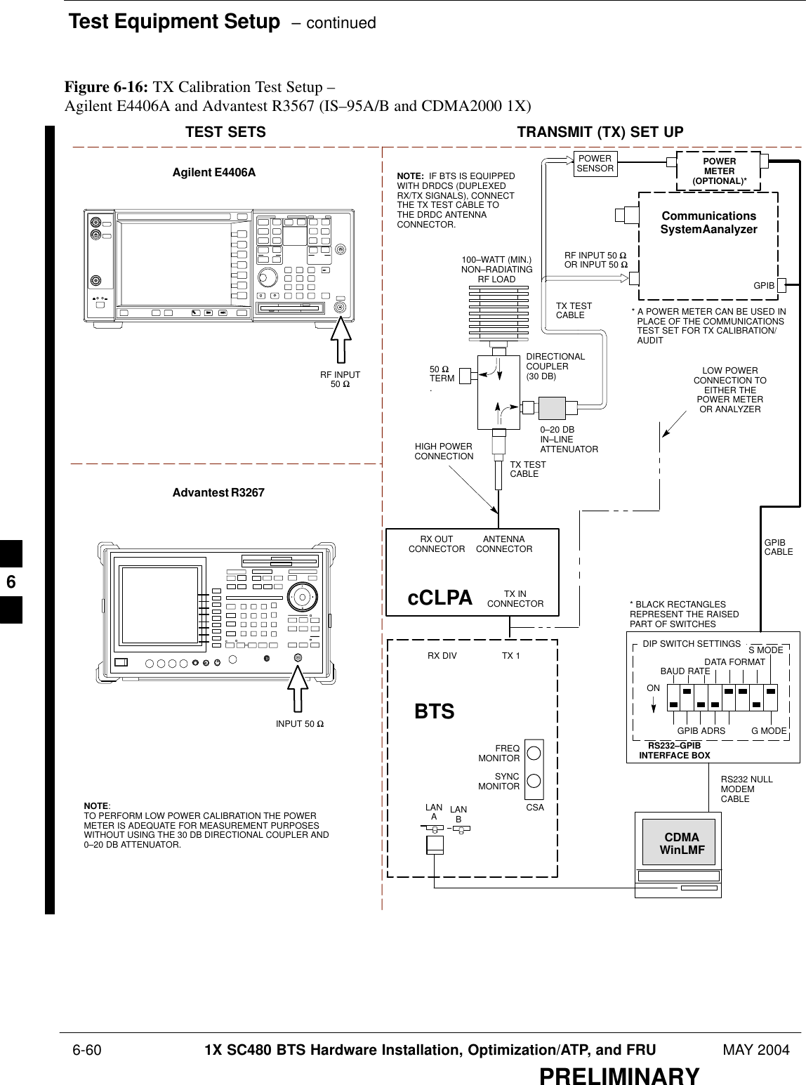
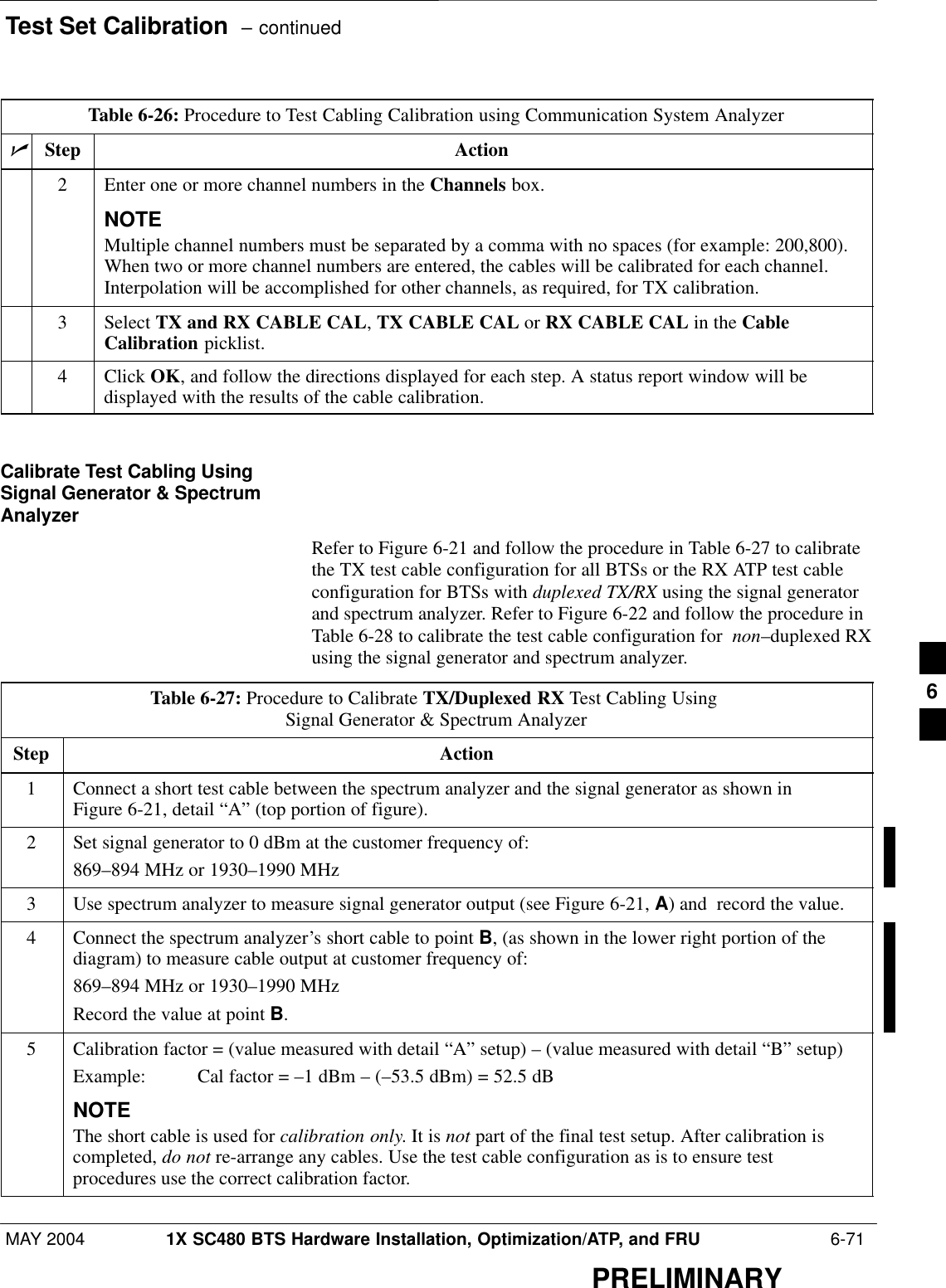
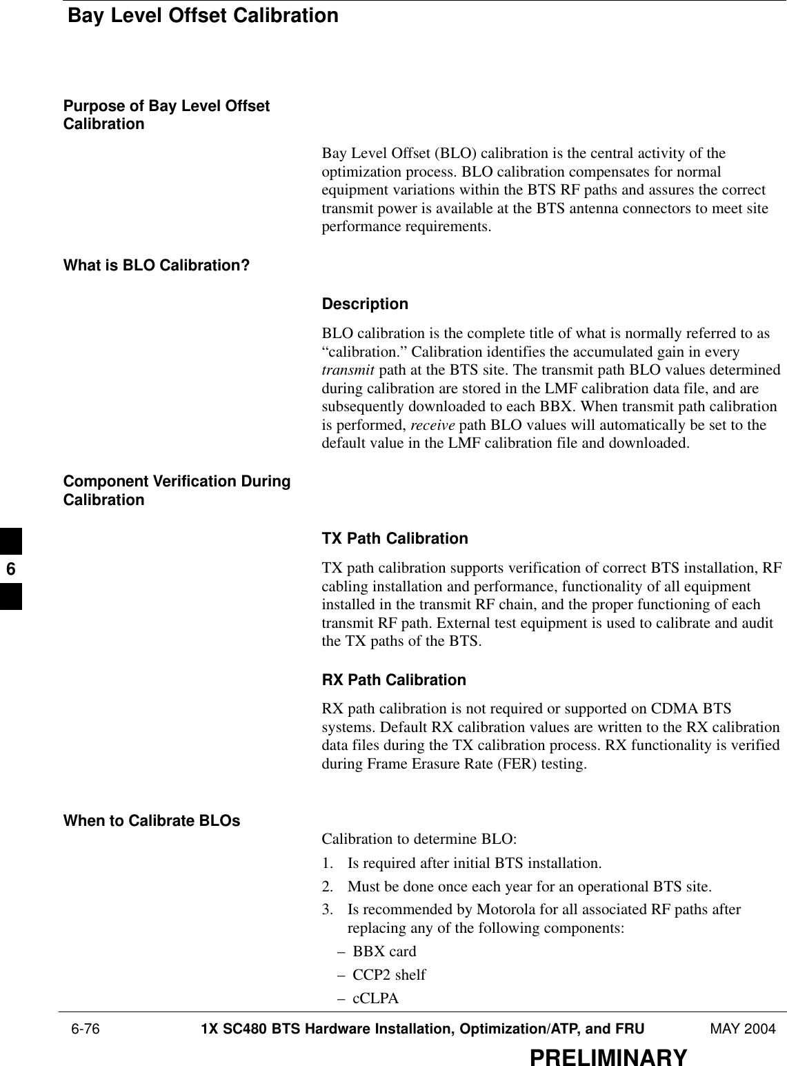
![Bay Level Offset Calibration – continued 6-78 1X SC480 BTS Hardware Installation, Optimization/ATP, and FRU MAY 2004PRELIMINARYCAL File and BLO Data DownloadWhen BLO data is downloaded to the BBXs after calibration, the data isdownloaded to the devices in the order it is stored in the CAL file. TXcalibration data (entries C[1] – C[60]) are sent first. Data for the tenBBX slot 1 calibration points (entries C[1] – C[20]) are sent initially,followed by data for the ten BBX slot 2 calibration points (entries C[21]– C[40]), and so on. The RX calibration data is sent next in BBX slotsequence, followed by RX Diversity calibration data.BLO for Expansion BTSThe BLO Ranges for expansion BTS configurations are listed below:Low PowerS1 to 4 carriers: –13 7 dBS5 to 8 carriers: –17 7dBHigh Power (1 or 2 cCLPAs)S1 to 4 carriers: 45 7 dBS5 to 8 carriers: 41 7dBTest Equipment Setup forRF Path CalibrationFollow the procedure in Table 6-31 and refer as needed to Figure 6-14 orFigure 6-15 to set up test equipment.Table 6-31: Procedure to Set Up Test Equipment for RF Path CalibrationStep Action1If it has not already been done, refer to the procedure in Table 6-6 (on page 6-17) to interface the LMFcomputer terminal to the frame LAN A connector.2If it has not already been done, refer to Table 6-7 (on page 6-25) to start a GUI LMF session.3If not already done, select test equipment per the procedure in Table 6-23 or Table 6-24.4If required, calibrate the test equipment per the procedure in Table 6-25.! CAUTIONTo prevent damage to the test equipment in high power configurations, all transmit (TX) testconnections must be via the 30 dB directional coupler for 800 MHz.Attenuators are not required for low power configuration.5For TX path calibration, connect the test equipment as shown in Figure 6-14, Figure 6-15, orFigure 6-16, depending on the communications analyzer being used.6](https://usermanual.wiki/Nokia-Solutions-and-Networks/T5EJ1.User-Manual-Part-2/User-Guide-430568-Page-94.png)