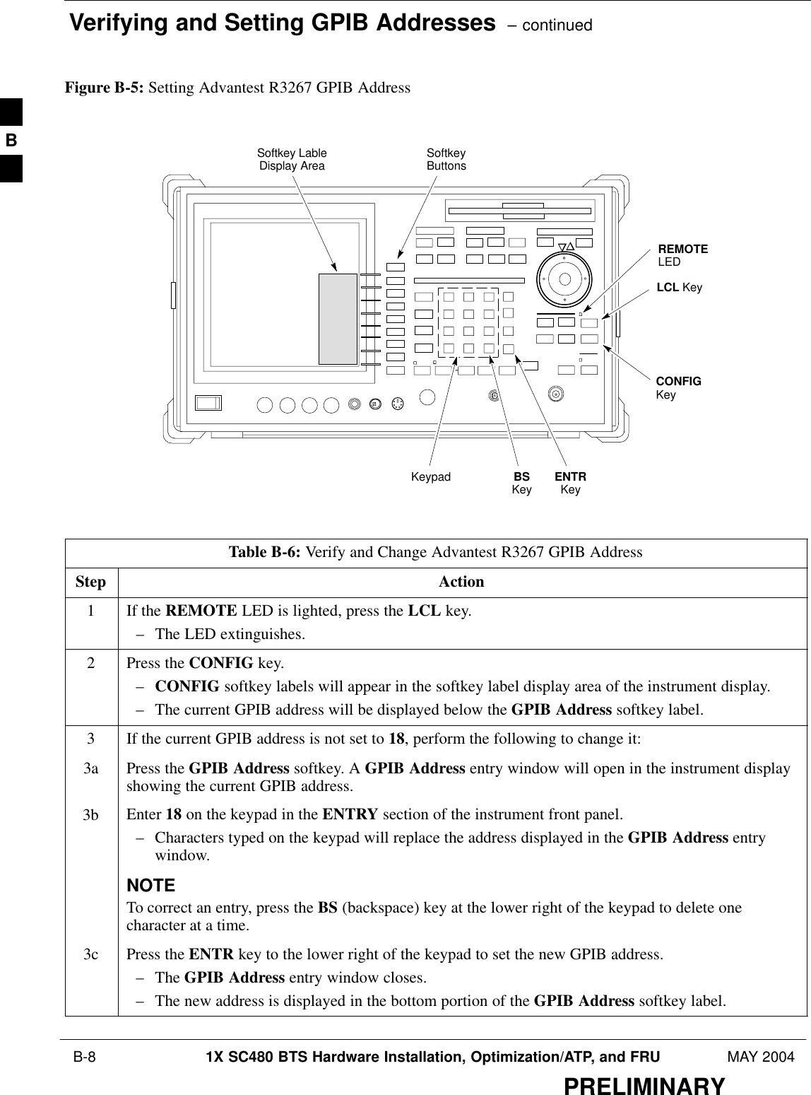
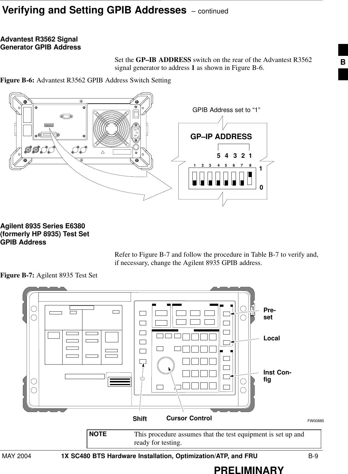
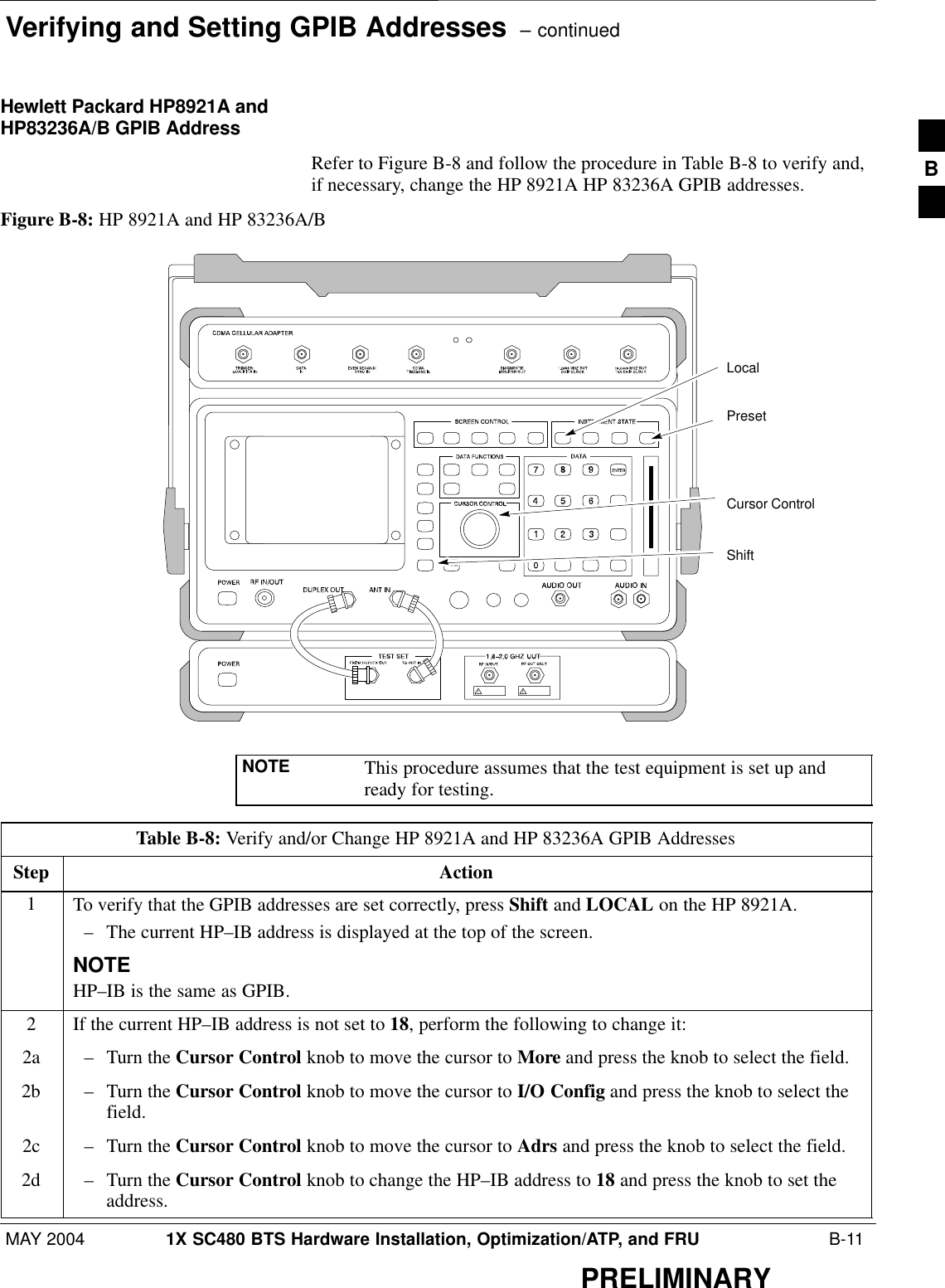
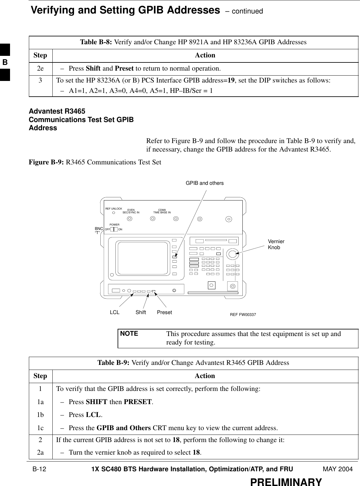
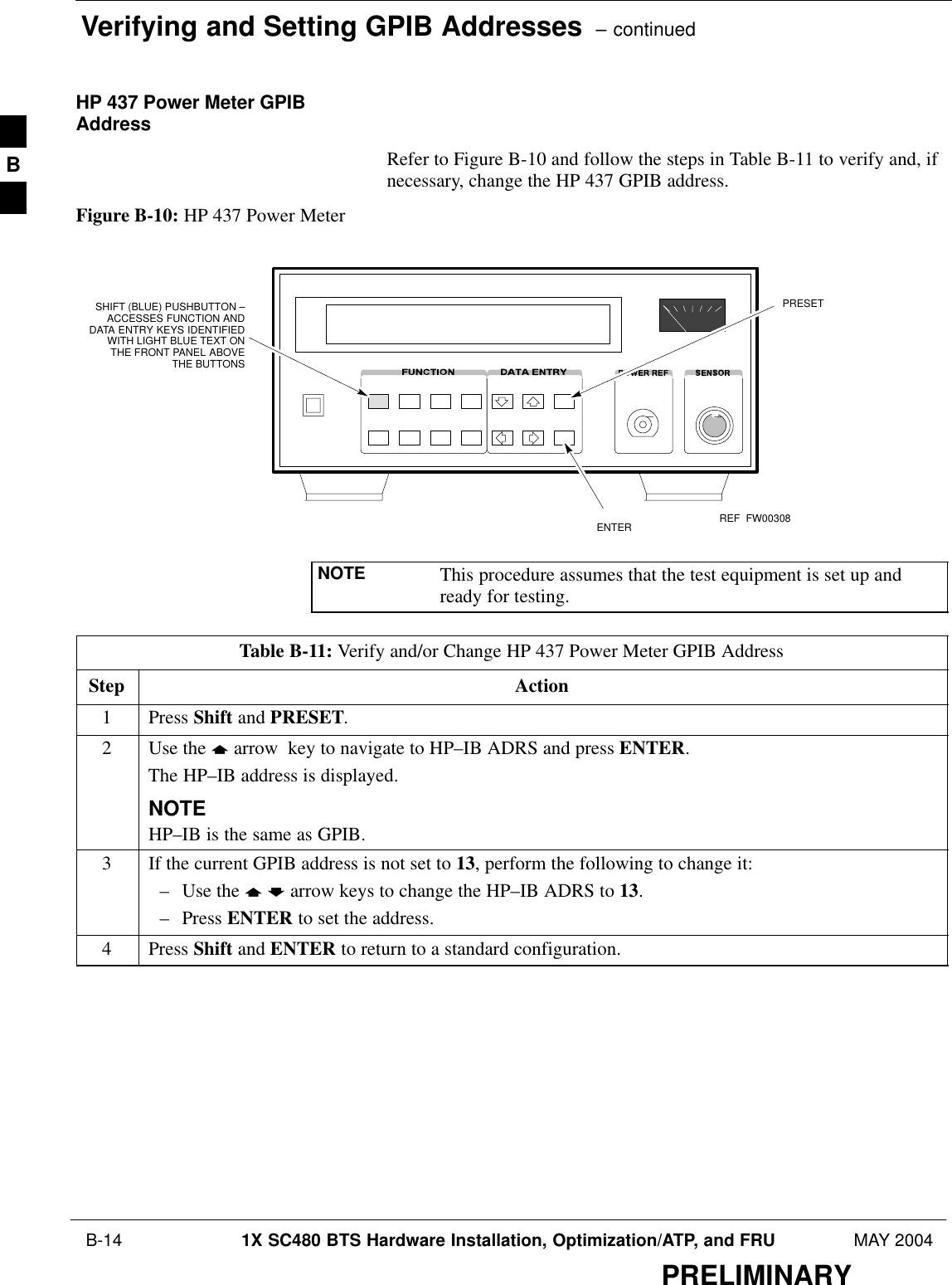
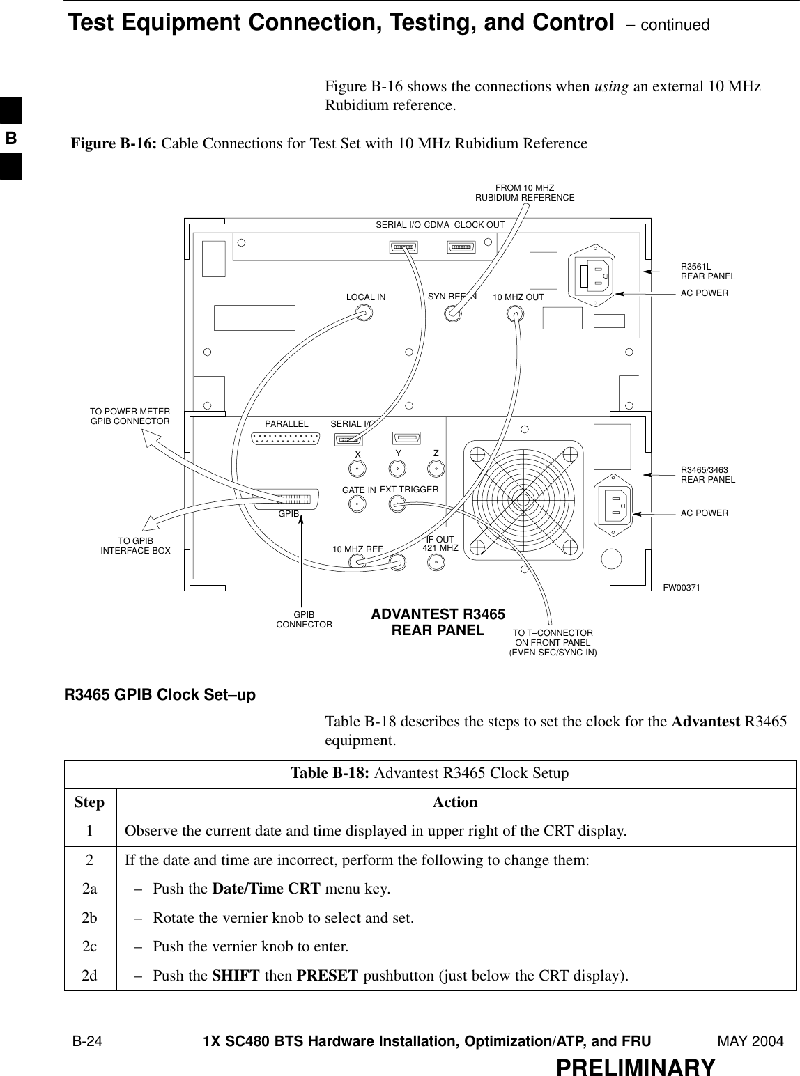
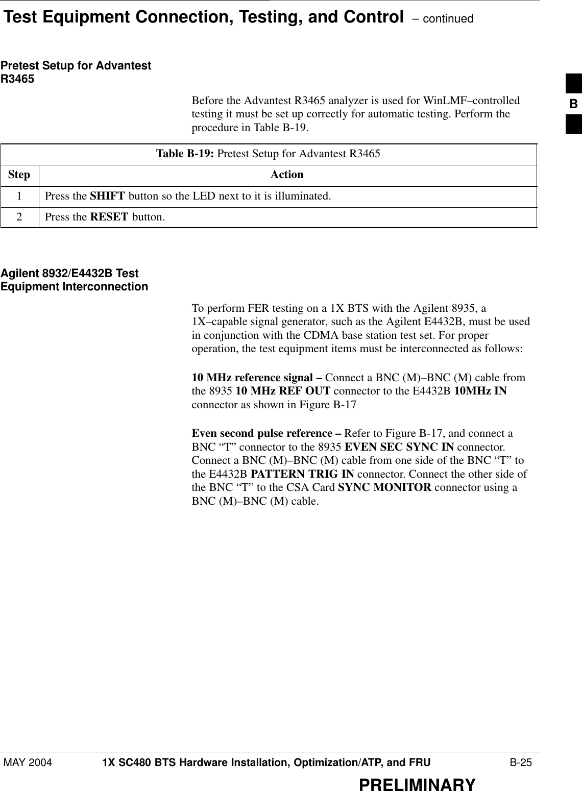
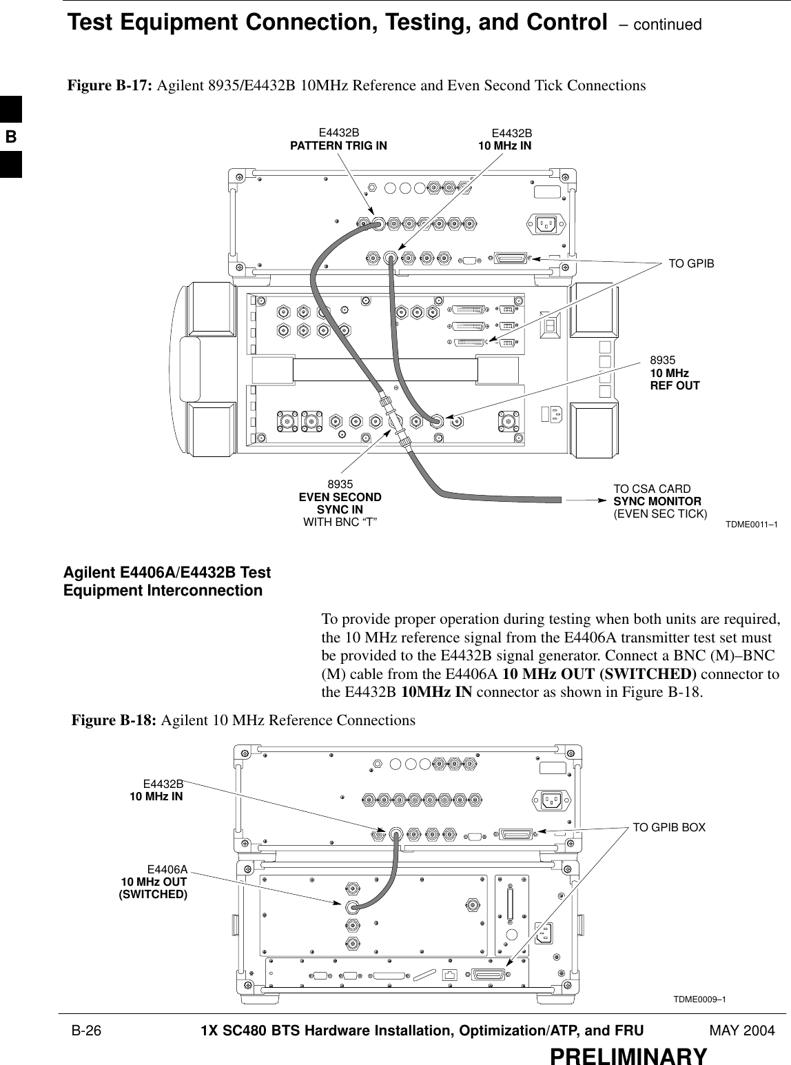
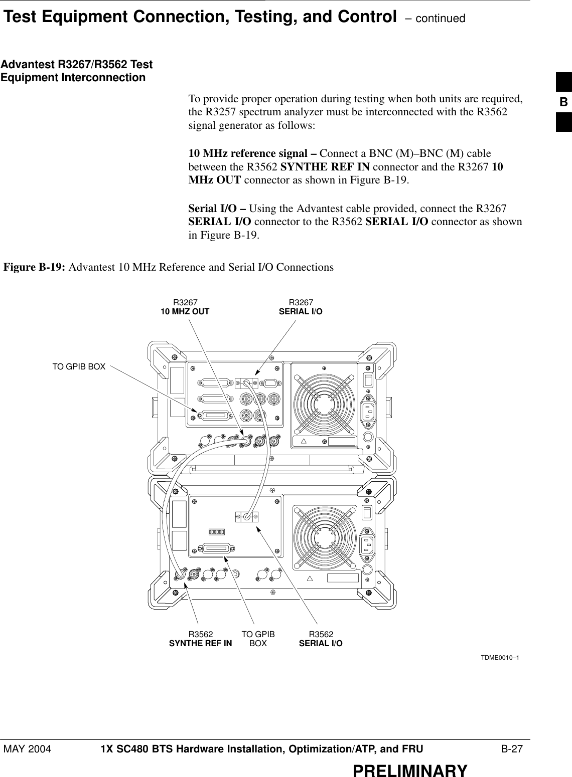
Nokia Solutions and Networks T5EJ1 1X SC480 BTS Microcell Base Station Transmitter User Manual print instructions
Nokia Solutions and Networks 1X SC480 BTS Microcell Base Station Transmitter print instructions
Contents
- 1. User Manual Part 1
- 2. User Manual Part 2
- 3. User Manual Part 3
- 4. User Manual Part 4
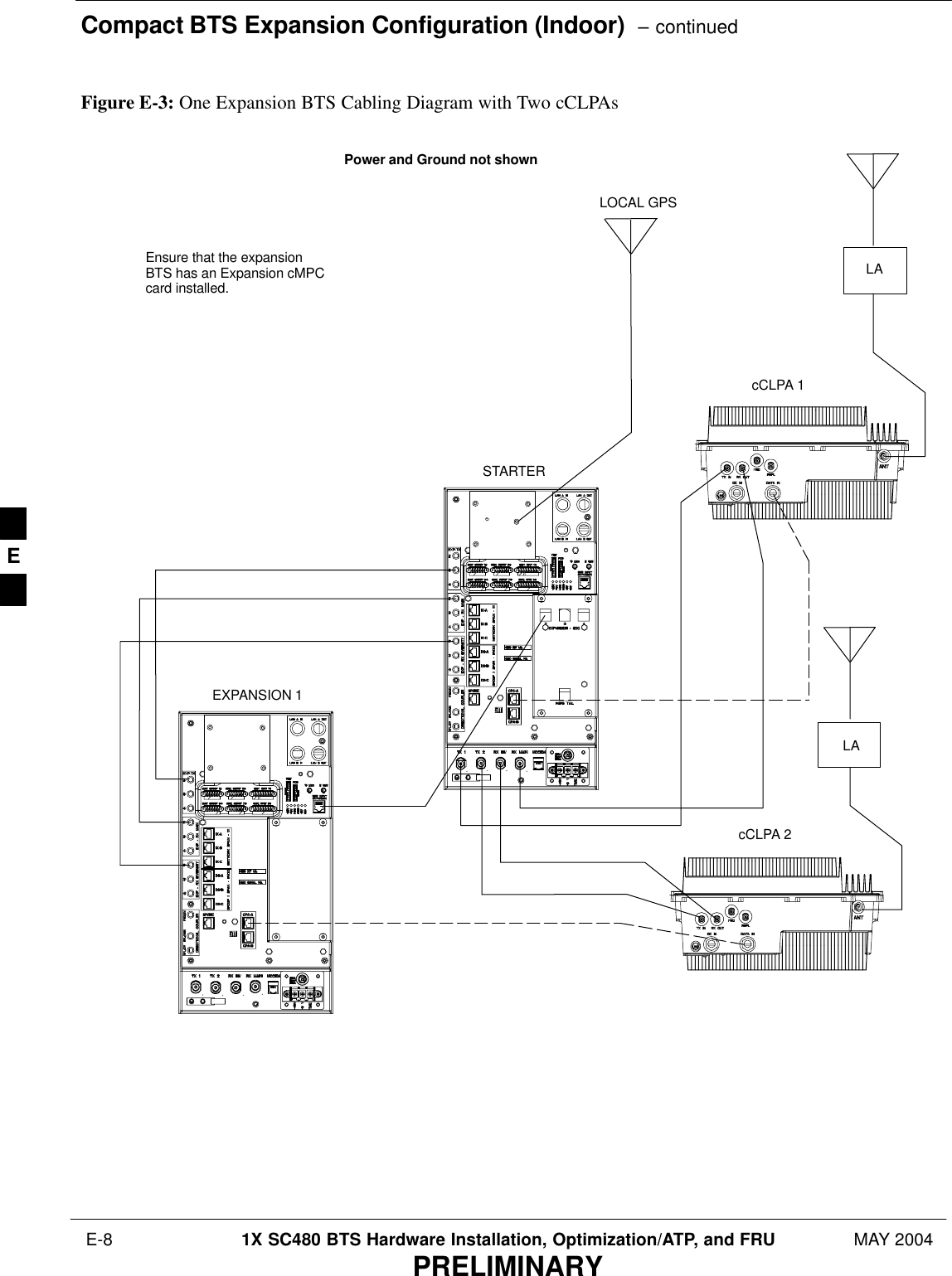
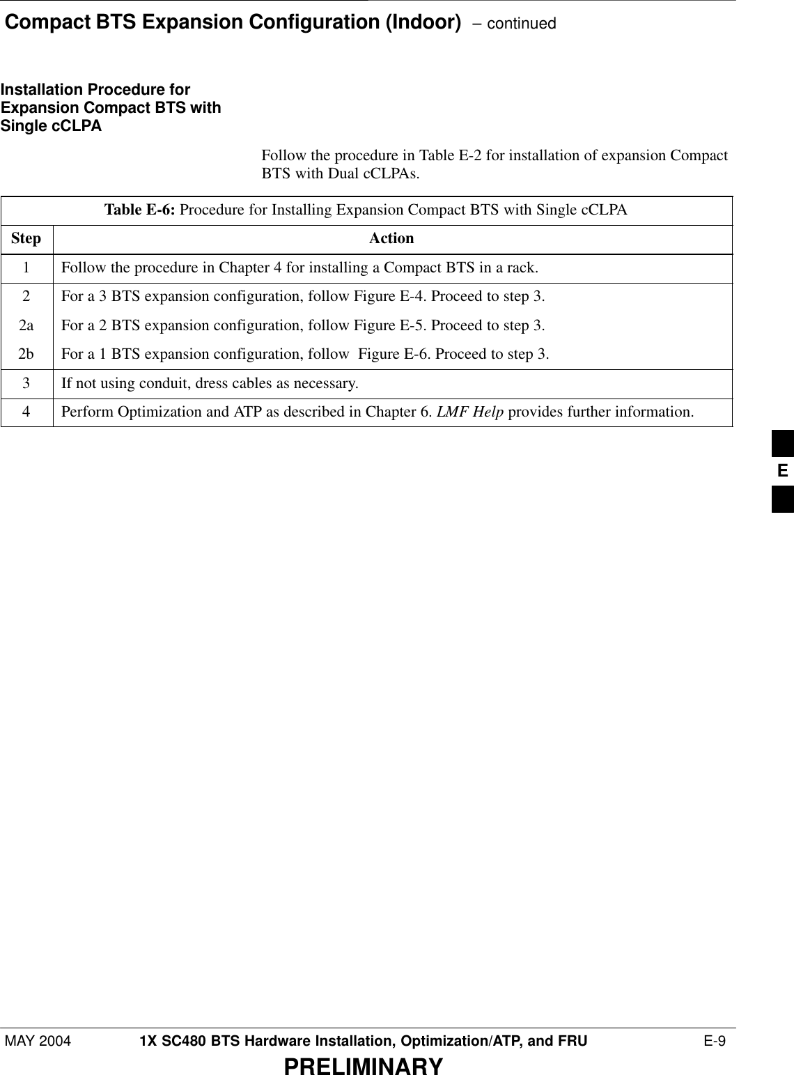
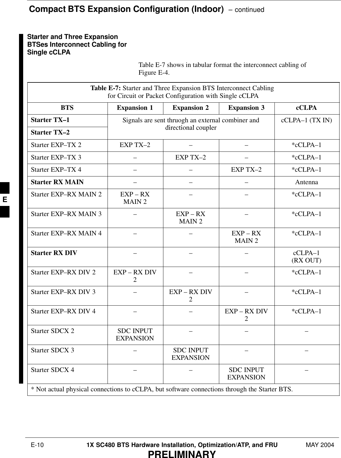
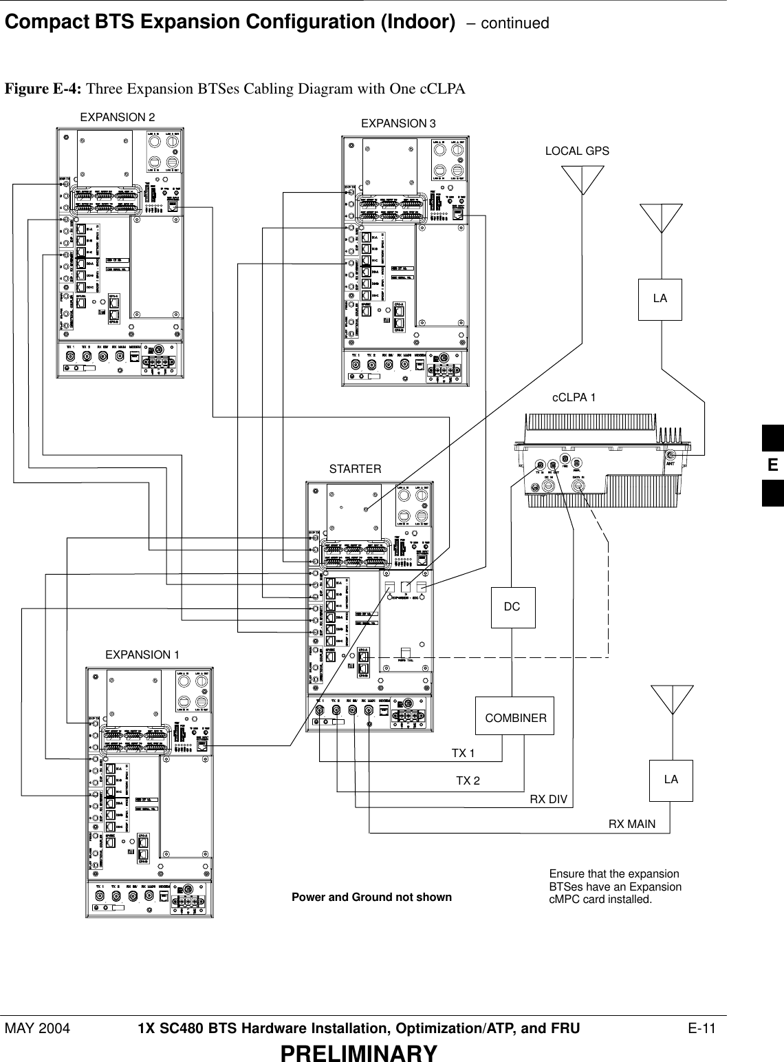
User Manual Part 4
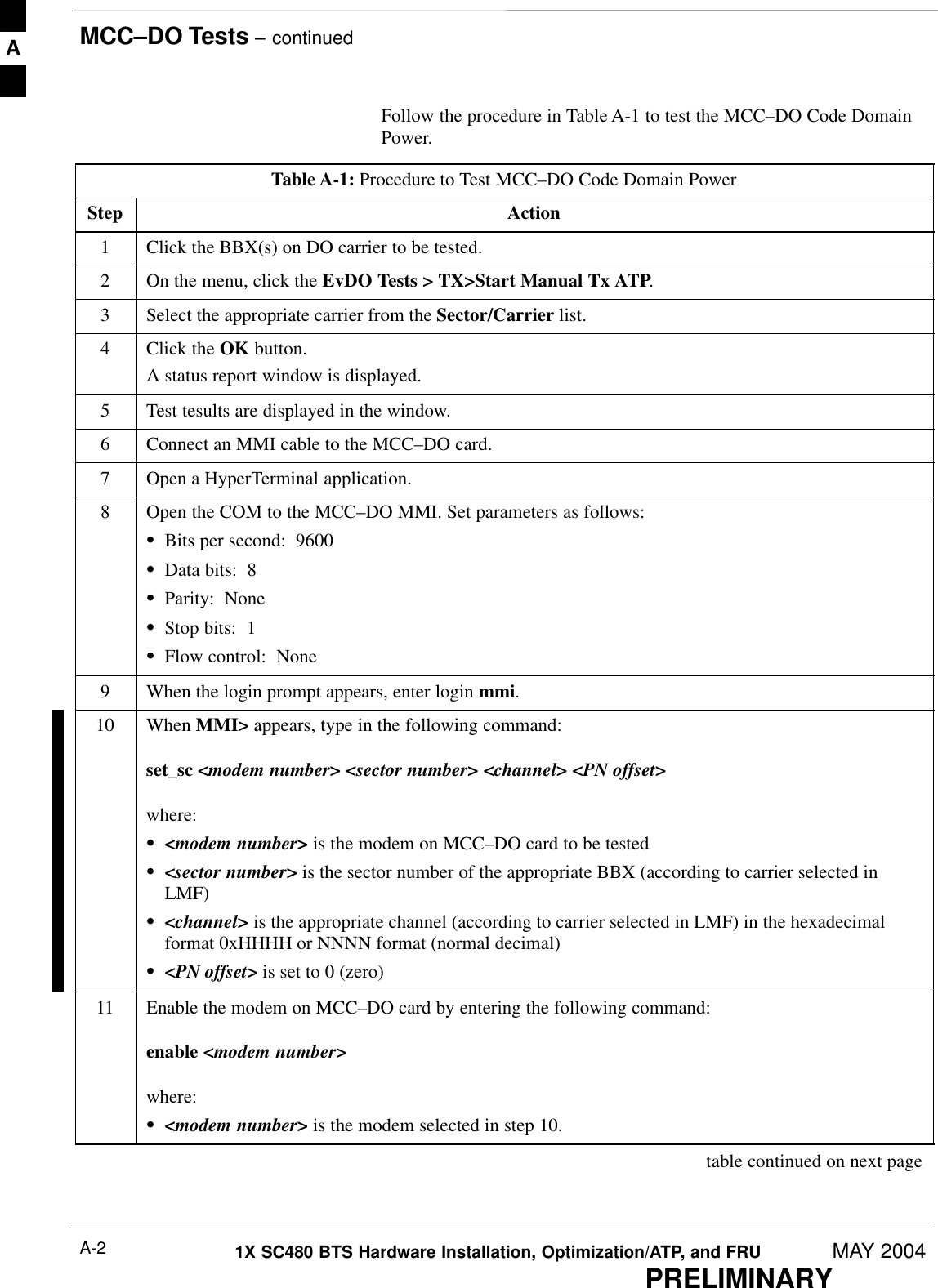
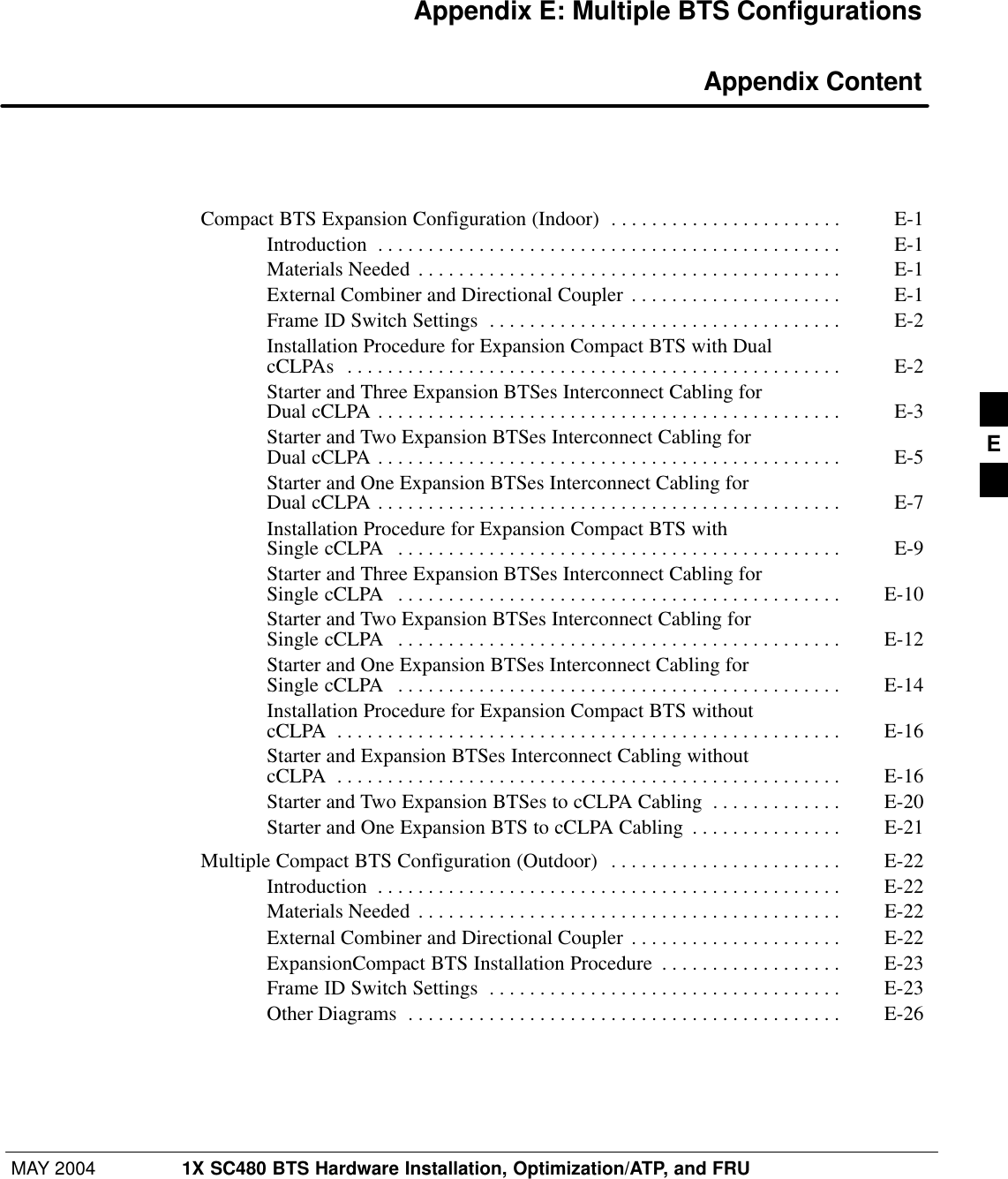
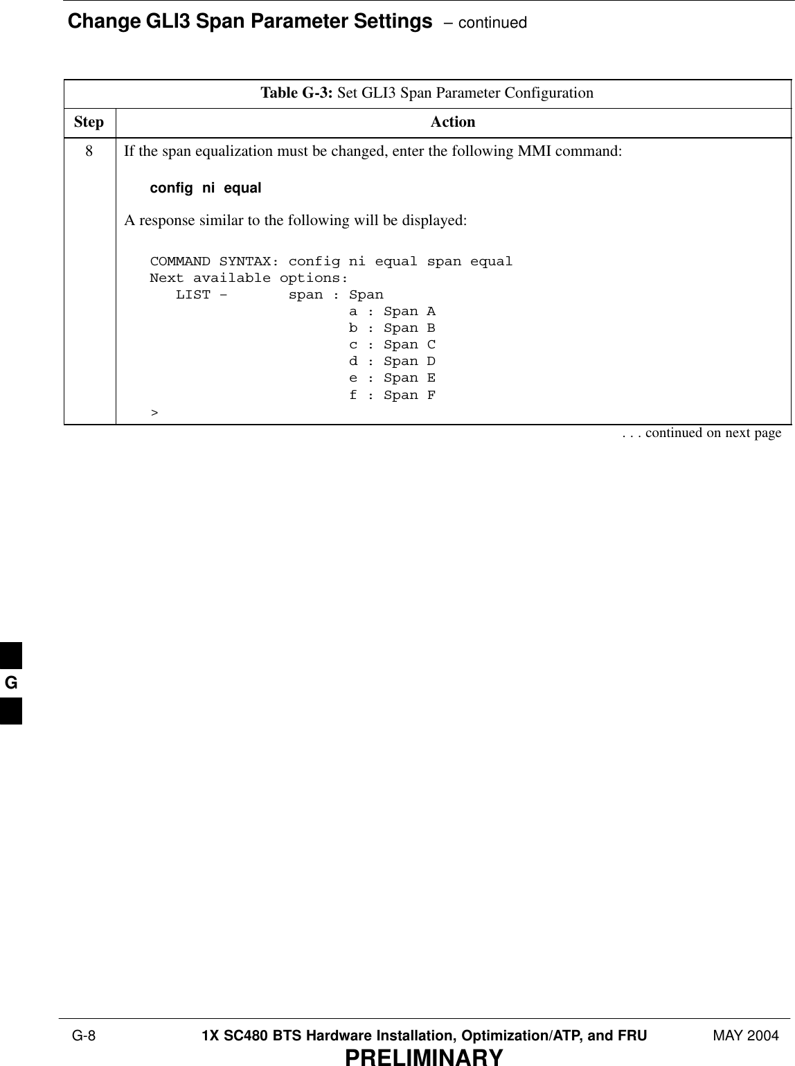
![MCC–DO Tests – continuedMAY 2004 A-31X SC480 BTS Hardware Installation, Optimization/ATP, and FRUPRELIMINARYTable A-1: Procedure to Test MCC–DO Code Domain PowerStep Action12 To generate a pattern, enter the following command:fl_pattern 313 On the Agilent E4406, set the Code Domain:SPress Measure buttonSPress More button until Code Domain option is displayedSSelect Code DomainSPress Meas Setup button, then press Meas Interval, enter 3.SPress Meas Control button, then press Measure to set it to ContSPress Meas Control buttonSSet Channel Type to MACSPress More button until Trig Source option is displayedSPress Trig Source key and select Ext Rear optionSPress More button until Advanced option is displayedSSelect Advanced optionSIf Chip Rate option is set to a value different than 1.228800, select Chip Rate and set it to1.228800SSelect Active Set Th option to a value calculated using the following formula:–xcvr_gain – cable_loss – 2dBSPress Display button and set the I/Q Combined Power Bar to OnSPress Display button, press Code Order button, select Hadamard optionSTo set appropriate frequency value, press Frequency and enter the value calculated according to thefollowing formula:–<tx_base_band_value> + 0.05*<chan_no> [MHz]14 Read the value of the power for each MAC channel.15 Note the Max Inactive Ch value. The Max Inactive Ch value is –31dB or lower. A](https://usermanual.wiki/Nokia-Solutions-and-Networks/T5EJ1.User-Manual-Part-4/User-Guide-430570-Page-13.png)
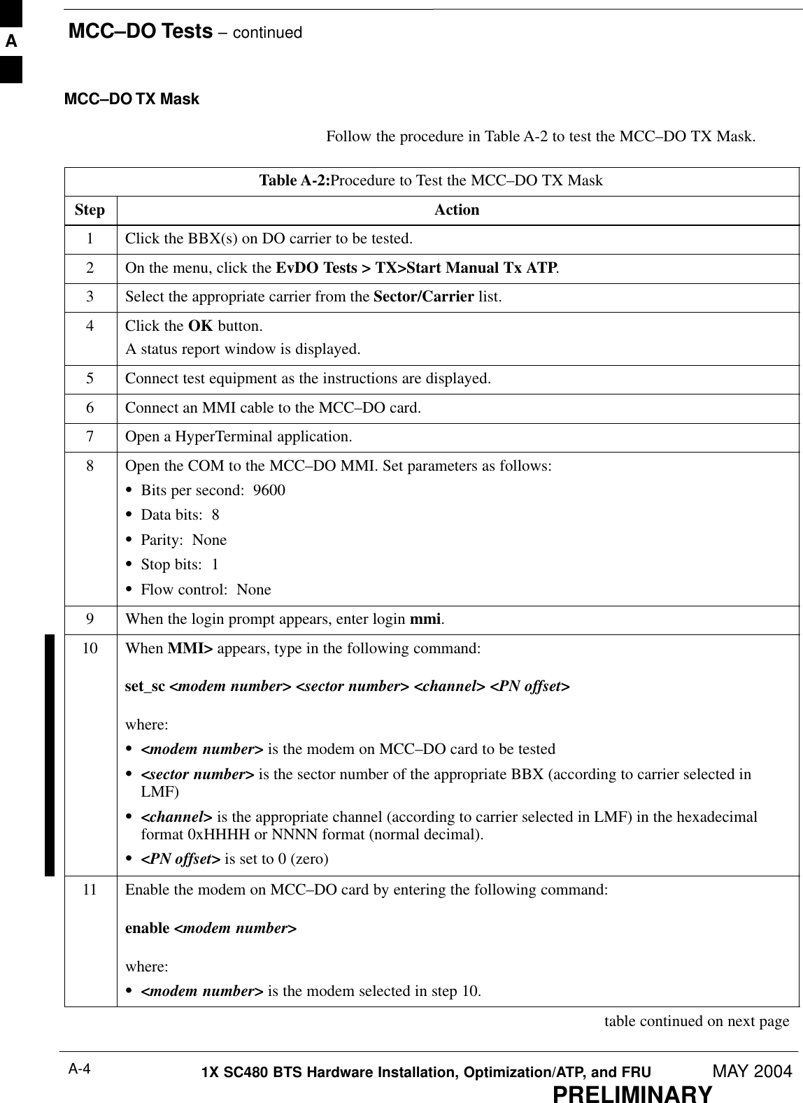
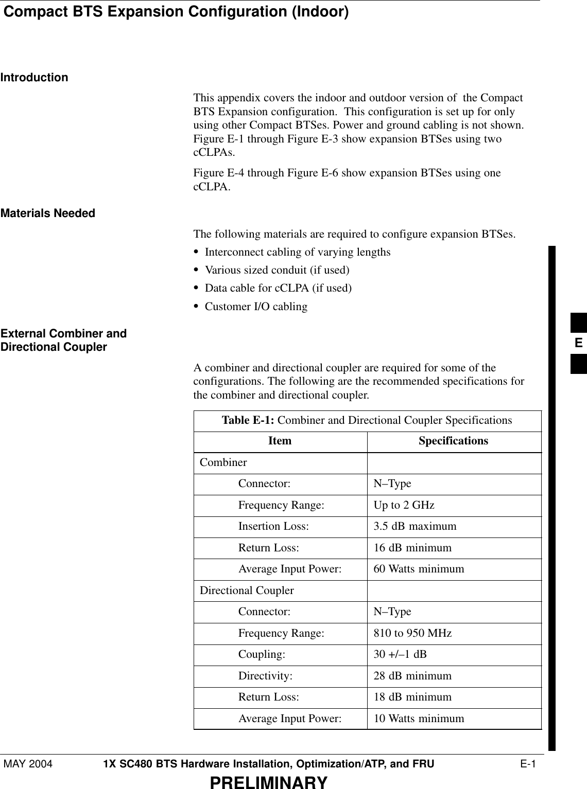
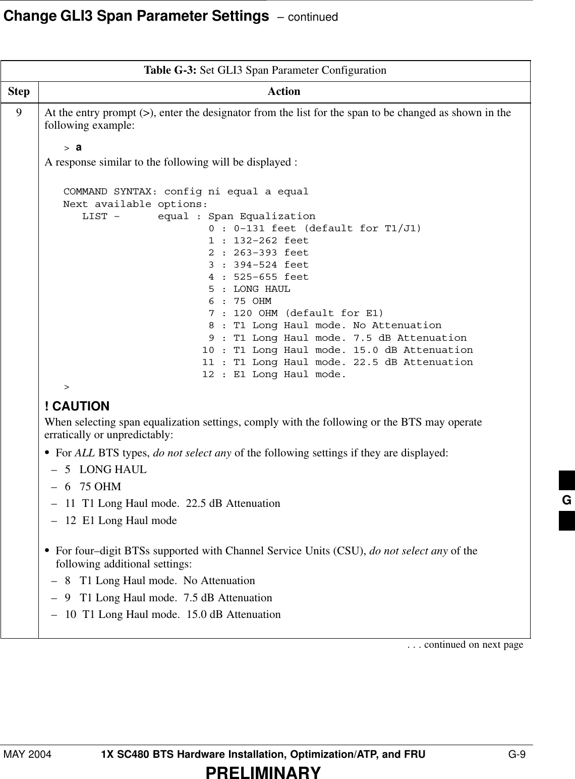
![MCC–DO Tests – continuedMAY 2004 A-51X SC480 BTS Hardware Installation, Optimization/ATP, and FRUPRELIMINARYTable A-2:Procedure to Test the MCC–DO TX MaskStep Action12 To generate a pattern, enter the following command:fl_pattern 313 On Agilent E4406, set Spectrum (Freq Domain) measurement as follows:SPress Measure buttonSPress More button until Spectrum (Freq Domain) option is displayedSSelect Spectrum optionSPress SPAN key to set its value to 4 [MHz]STo set the frequency value. press Frequency and enter the value calculated as follows:–<tx_base_band_value> + 0.05*<chan_no> [MHz]14 Use the formula from step 13 to calculate the four frequencies to measure the Power.Scheck_point_1 = freq – 750 [kHz]Scheck_point_2 = freq + 750[kHz]Scheck_point_3 = freq – 1980 [kHz]Scheck_point_4 = freq + 1980 [kHz]15 Press MARKER key:SSelect 1, 2, 3, or 4 (frequency points)SPress FUNCTION key and select Off optionSPress TRACE key and select Spectrum optionSPress NORMAL keySUse the numeric keypad to enter the calculated frequency, assigning the proper unit.SNote the Power value of markerSRepeat step for all calculated frequency checkpointsThe check point values are as follows:SCheck_point_1 > –40 dBmSCheck_point_2 > –40 dBmSCheck_point_3 > –60 dBmSCheck_ point_4 > –60 dBm A](https://usermanual.wiki/Nokia-Solutions-and-Networks/T5EJ1.User-Manual-Part-4/User-Guide-430570-Page-15.png)
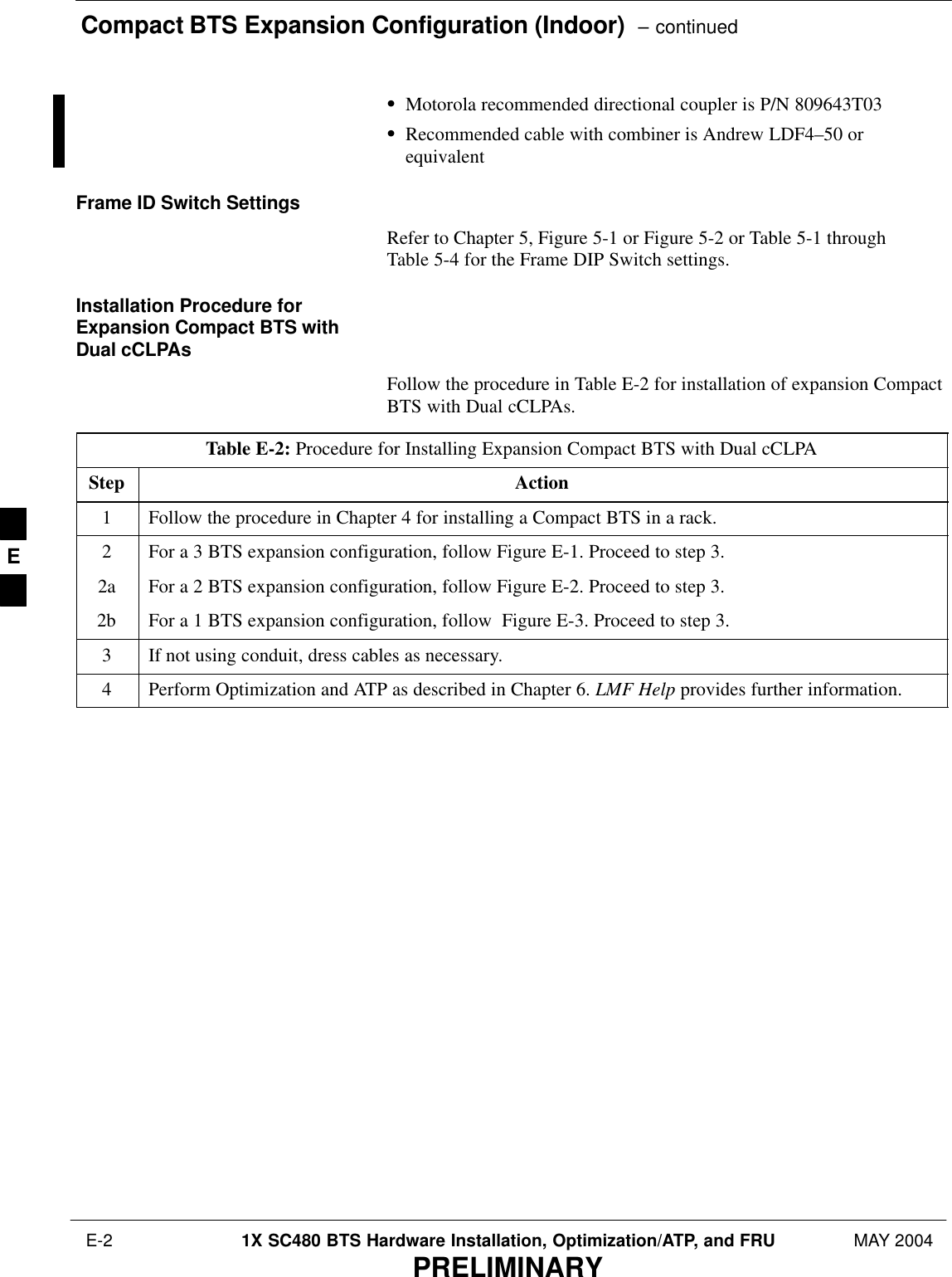
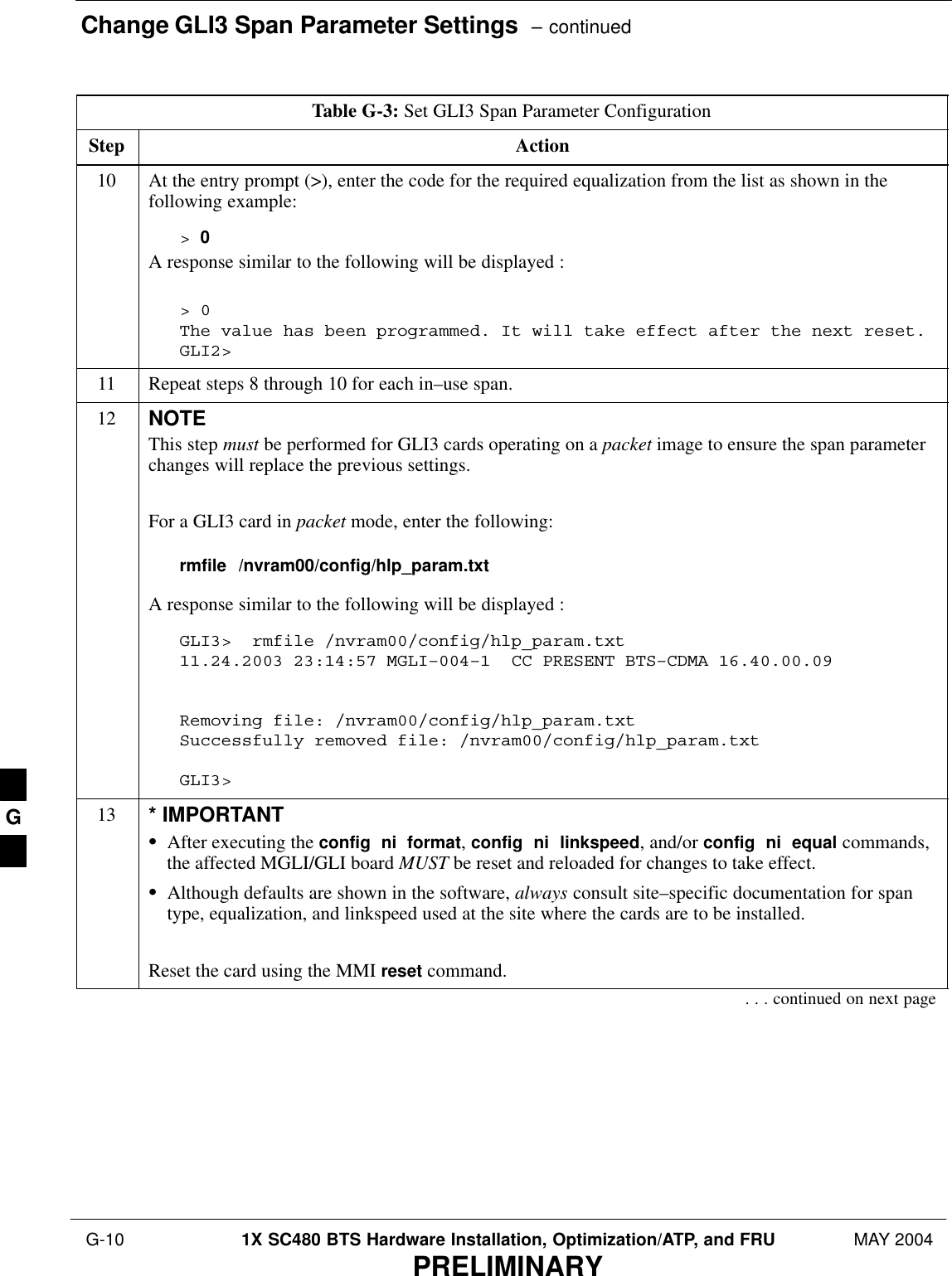
![MCC–DO Tests – continuedMAY 2004 A-71X SC480 BTS Hardware Installation, Optimization/ATP, and FRUPRELIMINARYTable A-3: Procedure to Test MCC–DO Pilot Time OffsetStep Action9 When MMI> appears, type in the following command:set_sc <modem number> <sector number> <channel> <PN offset>where:S<modem number> is the modem on MCC–DO card to be testedS<sector number> is the sector number of the appropriate BBX (according to carrier selected inLMF)S<channel> is the appropriate channel (according to carrier selected in LMF) in the hexadecimalformat 0xHHHH or NNNN format (normal decimal).S<PN offset> is set to 0 (zero)10 Enable the modem on MCC–DO card by entering the following command:enable <modem number>where:S<modem number> is the modem selected in step 10.11 To generate a pattern, enter the following command:fl_pattern 312 On the Agilent E4406, set the Mod Accuracy (composite Rho) measurement:SPress Measure buttonSPress More button until Mod Accuracy (composite Rho) option is displayedSSelect Mod Accuracy (composite Rho)SPress Meas Setup buttonSPress More button until Trig Source option is displayedSPress Trig Source key and select Ext Rear optionSPress More button until Advanced option is displayedSSelect Advanced optionSIf Chip Rate option is set to a value different than 1.228800, select Chip Rate and set it to1.228800SSelect Active Set Th option to a value calculated using the following formula:–xcvr_gain – cable_loss – 2dBSTo set appropriate frequency value, press Frequency and enter the value calculated according to thefollowing formula:–<tx_base_band_value> + 0.05*<chan_no> [MHz]13 Read the value of thePilot Offset. The Pilot Offset is less than 3 microseconds A](https://usermanual.wiki/Nokia-Solutions-and-Networks/T5EJ1.User-Manual-Part-4/User-Guide-430570-Page-17.png)
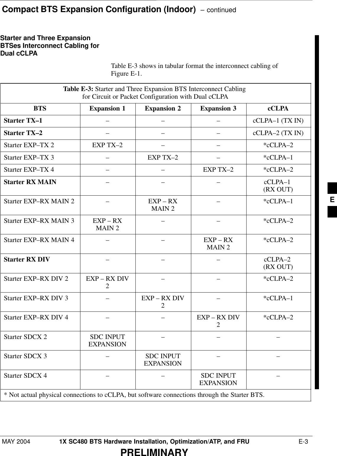
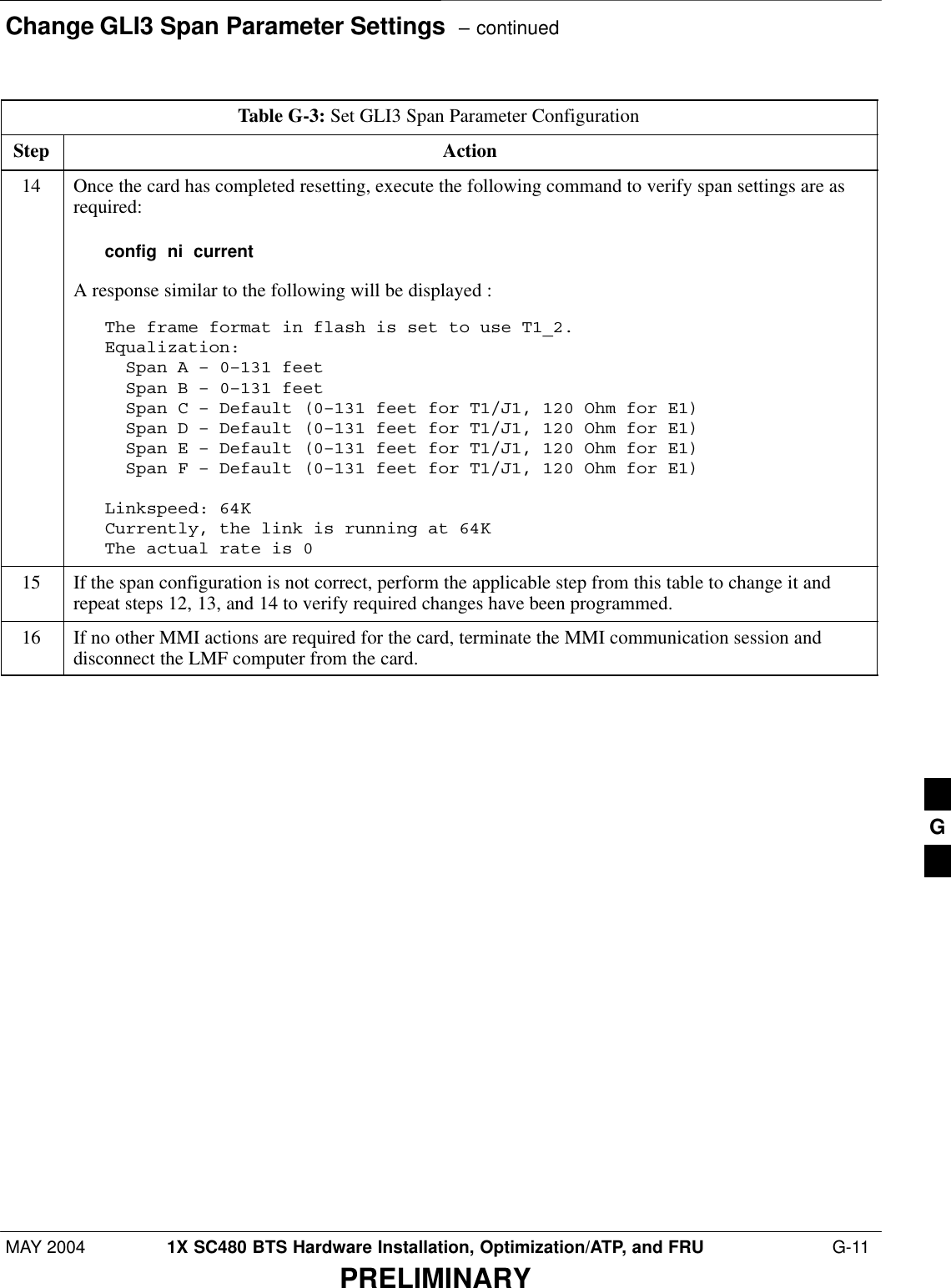
![MCC–DO Tests – continuedMAY 2004 A-91X SC480 BTS Hardware Installation, Optimization/ATP, and FRUPRELIMINARYTable A-4: Procedure to Test MCC–DO RhoStep Action10 Enable the modem on MCC–DO card by entering the following command:enable <modem number>where:S<modem number> is the modem selected in step 10.11 To generate a pattern, enter the following command:fl_pattern 312 On the Agilent E4406, set the Mod Accuracy (composite Rho) measurement:SPress Measure buttonSPress More button until Mod Accuracy (composite Rho) option is displayedSSelect Mod Accuracy (composite Rho)SPress Meas Setup buttonSPress More button until Trig Source option is displayedSPress Trig Source key and select Ext Rear optionSPress More button until Advanced option is displayedSSelect Advanced optionSIf Chip Rate option is set to a value different than 1.228800, select Chip Rate and set it to1.228800SSelect Active Set Th option to a value calculated using the following formula:–xcvr_gain – cable_loss – 2dBSTo set appropriate frequency value, press Frequency and enter the value calculated according to thefollowing formula:–<tx_base_band_value> + 0.05*<chan_no> [MHz]13 Read the value of the Rho. Rho normalized cross coefficient ( ò ) is greater than 0.912 MCC–DO Packet Error RateThe PER test verifies PER (Packet Error Rate) of traffic channels of anXCVR carrier keyed up at a specific frequency per the current CDF file.The XCVR is keyed to generate a CDMA carrier (with pilot channelelement only) of the correct level.The calibrated communications test set measures the all zero long codeand verifies that the PER is not greater than 1 percent. A total number ofpackets to be received is dependent on Rate Set chosen.PER PrerequisitesTo perform the following test, the Agilent E4432B Signal Generatormust have the following installed:A](https://usermanual.wiki/Nokia-Solutions-and-Networks/T5EJ1.User-Manual-Part-4/User-Guide-430570-Page-19.png)
![MCC–DO Tests – continuedMAY 2004 A-111X SC480 BTS Hardware Installation, Optimization/ATP, and FRUPRELIMINARYTable A-5: Procedure to Test MCC–DO Packet Error RateStep Action6Enter the following parameters for signal generation.Channel Configuration:SRRI Channel – checked RRI Bits – 1SDRC Channel – checked Rel. gain (dB) – 3SACK Channel – checked Rel. gain (dB) – 0SData Channel – checked Rel. gain (dB) – 3.75SData Channel encoder active – checkedSData Channel Data rate – 9.6 kbpsSData Channel bit stream – PN15SI Mask – 3FF80000000SQ Mask – 3FF00000001 Signal Generation:SOversampling ratio – 4SFilter Type – IS 95 StdSMirror Spectrum – uncheckedESG Configuration:SFrequency – calculated according to the formula: <rx_base_band_value> + 0,05 * <chan_no>[MHz]SAmplitude – depending on attenuation applied – overall signal value should be –122 [dBm]SSampling rate 4.1952 [MHz]SReconstruction filter 2.5 [MHz]SRF Blanking – uncheckedSInternal ReferenceS+ Mkrs7 Press Time Slot Setup button and set the following parameters:ACK ChannelSActive – All OnSData – 0sDRC ChannelSActive – All OnSData – F (1111)SCover – 18 Press DOWNLOAD button on the ”Agilent Signal Studio – 1xEV Reverse Link” application. table continued on next pageA](https://usermanual.wiki/Nokia-Solutions-and-Networks/T5EJ1.User-Manual-Part-4/User-Guide-430570-Page-21.png)

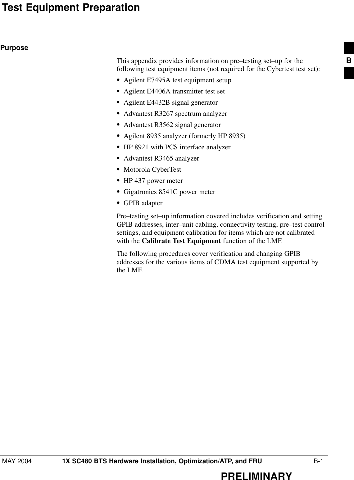
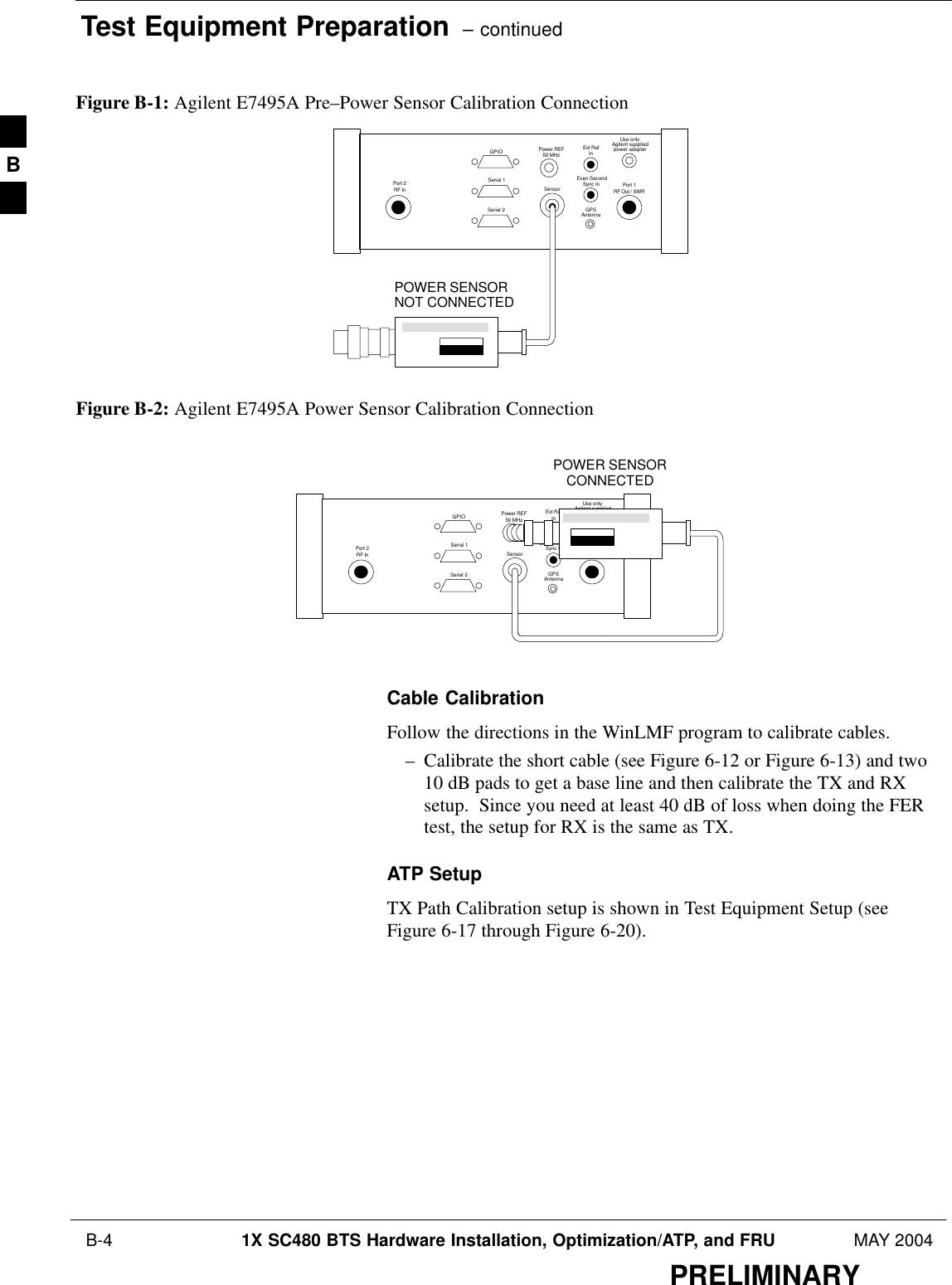
![Test Equipment Preparation – continued B-2 1X SC480 BTS Hardware Installation, Optimization/ATP, and FRU MAY 2004PRELIMINARYAgilent R7495A Test EquipmentSetupThis test equipment requires a warm-up period of at least 30 minutesbefore BTS testing or calibration begins.Using the Agilent E7495A with the LMFThe Agilent E7495A does not require the use of the 19MHz frequencyreference; if connected, it will be ignored. The Even Sec SYNCconnection is required.The Agilent E7495A signal generator is only calibrated down to –80db.In order to achieve accurate FER testing, be sure the RX setup includesat least 40db of attenuation. This will ensure the signal generator willoutput sufficient power to operate in the calibrated range.Set the IP Address as described in Table B-1.Table B-1: Set IP Address on Agilent E7495A test setnStep Action1Use the System Button > Controls >IPAdmin to set an IP address on the E7495A as 128.0.0.49,and Netmask to 255.255.255.128. ConnectionsIt is recommended that you use a hub with BNC and RJ–45 connections.[Suggested models: Netgear model EN104 (4 port) or EN108 (8 port).Do NOT use model numbers ending with “TP”; those have no BNCconnectors.]The LMF will connect to the hub which in turn is connected to the BTSand to the Agilent E7495A.Agilent E7495A to Hub – This is an Ethernet cable, RJ–45 to RJ–45.LMF to Hub – Use one of the following cables to connect the LMF tothe Hub:– Ethernet cable, RJ–45 to RJ–45 (be sure that the LAN card is set foreither AUTO or to use the RJ–45 only).– Coax cable between LAN card and Hub. (Use a “T” on the hub andconnect a cable between the other end of the “T” and the BTS LANconnection).Hub to BTS – Use BNC “T” connector on the hub. [If your hub doesn’thave BNC ports, use a BNC to UTP adapter.]B](https://usermanual.wiki/Nokia-Solutions-and-Networks/T5EJ1.User-Manual-Part-4/User-Guide-430570-Page-28.png)
![Test Equipment Connection, Testing, and Control – continuedMAY 2004 1X SC480 BTS Hardware Installation, Optimization/ATP, and FRU B-21PRELIMINARYHP 8921A with PCS InterfaceSystem Connectivity TestFollow the steps outlined in Table B-15 to verify that the connectionsbetween the PCS Interface and the HP 8921A are correct and cables areintact. The software also performs basic functionality checks of eachinstrument.Disconnect other GPIB devices, especially systemcontrollers, from the system before running theconnectivity software.NOTETable B-15: System ConnectivityStep ActionNOTE– Perform this procedure after test equipment has been allowed to warm–up and stabilize for aminimum of 60 minutes.1Insert HP 83236A Manual Control/System card into memory card slot.2Press the [PRESET] pushbutton.3Press the Screen Control [TESTS] pushbutton to display the “Tests” Main Menu screen.4Position the cursor at Select Procedure Location and select it by pressing the cursor control knob. Inthe Choices selection box, select Card.5Position the cursor at Select Procedure Filename and select it by pressing the cursor control knob. Inthe Choices selection box, select SYS_CONN.6Position the cursor at RUN TEST and select it. The software will provide operator prompts throughcompletion of the connectivity setup.7Do the following when the test is complete,Sposition cursor on STOP TEST and select itSOR press the [K5] pushbutton.8To return to the main menu, press the [K5] pushbutton.9Press the [PRESET] pushbutton. Pretest Setup for HP 8921ABefore the HP 8921A CDMA analyzer is used for WinLMF–controlledtesting it must be set up correctly for automatic testing. Perform theprocedure in Table B-16.B](https://usermanual.wiki/Nokia-Solutions-and-Networks/T5EJ1.User-Manual-Part-4/User-Guide-430570-Page-47.png)
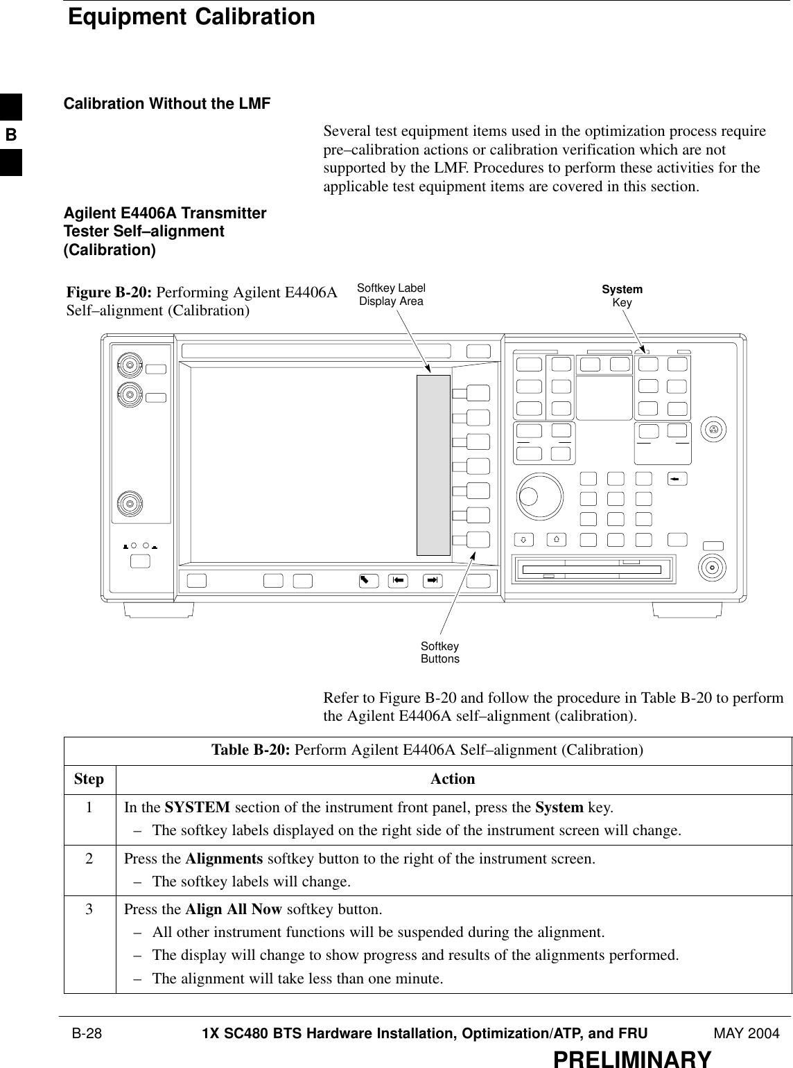
![Equipment Calibration – continuedMAY 2004 1X SC480 BTS Hardware Installation, Optimization/ATP, and FRU B-29PRELIMINARYCalibrating HP 437 PowerMeterPrecise transmit output power calibration measurements are made usinga bolometer–type broadband power meter with a sensitive power sensor.Follow the steps outlined in Table B-21 to enter information unique tothe power sensor before calibrating the test setup. Refer to Figure B-21as required.NOTE This procedure must be done before the automated calibration toenter power sensor specific calibration values.Figure B-21: Power Meter DetailCONNECT POWERSENSOR WITH POWERMETER TURNED OFFCONNECT POWER SENSORTO POWER REFERENCEWHEN CALIBRATING UNIT.POWER REFERENCE ISENABLED USING THE SHIFT ’KEYSSHIFT (BLUE) PUSHBUTTON –ACCESSES FUNCTION ANDDATA ENTRY KEYS IDENTIFIEDWITH LIGHT BLUE TEXT ONTHE FRONT PANEL ABOVETHE BUTTONSFW00308Table B-21: HP 437 Power Meter Calibration ProcedureStep Action1! CAUTIONDo not connect/disconnect the power meter sensor cable with AC power applied to the meter.Disconnection could result in destruction of the sensing element or mis–calibration.Make sure the power meter AC LINE pushbutton is OFF.2Connect the power sensor cable to the SENSOR input.3Set the AC LINE pushbutton to ON.NOTEThe calibration should be performed only after the power meter and sensor have been allowed towarm–up and stabilize for a minimum of 60 minutes.4Perform the following to set or verify the correct power sensor model:4a – Press [SHIFT] then [a] to select SENSOR.4b – Identify the power sensor model number from the sensor label.4c – Use the [y] or [b] button to select the appropriate model; then press [ENTER].5Refer to the illustration for step 8, and perform the following to ensure the power reference output isOFF:. . . continued on next pageB](https://usermanual.wiki/Nokia-Solutions-and-Networks/T5EJ1.User-Manual-Part-4/User-Guide-430570-Page-55.png)
![Equipment Calibration – continued B-30 1X SC480 BTS Hardware Installation, Optimization/ATP, and FRU MAY 2004PRELIMINARYTable B-21: HP 437 Power Meter Calibration ProcedureStep Action5a – Observe the instrument display and determine if the triangular indicator over PWR REF isdisplayed.5b – If the triangular indicator is displayed, press [SHIFT] then [’] to turn it off.6 Press [ZERO].– Display will show “Zeroing ******.”– Wait for process to complete.7Connect the power sensor to the POWER REF output.8Turn on the PWR REF by performing the following:8a – Press [SHIFT] then [’].8b – Verify that the triangular indicator (below) appears in the display above PWR REF.9Perform the following to set the REF CF%:9a – Press ([SHIFT] then [ZERO]) for CAL.9b – Enter the sensor’s REF CF% from the sensor’s decal using the arrow keys and press [ENTER].(The power meter will display ”CAL *****” for a few seconds.)NOTEIf the REF CAL FACTOR (REF CF) is not shown on the power sensor, assume it to be 100%.10 Perform the following to set the CAL FAC %:10a – Press [SHIFT] then [FREQ] for CAL FAC.10b – On the sensor’s decal, locate an approximate calibration percentage factor (CF%) at 2 GHz.10c – Enter the sensor’s calibration % (CF%) using the arrow keys and press [ENTER].–– When complete, the power meter will typically display 0.05 dBm. (Any reading between0.00 and 0.10 is normal.)11 To turn off the PWR REF, perform the following:11a – Press [SHIFT] then [’].11b – Disconnect the power sensor from the POWER REF output. B](https://usermanual.wiki/Nokia-Solutions-and-Networks/T5EJ1.User-Manual-Part-4/User-Guide-430570-Page-56.png)
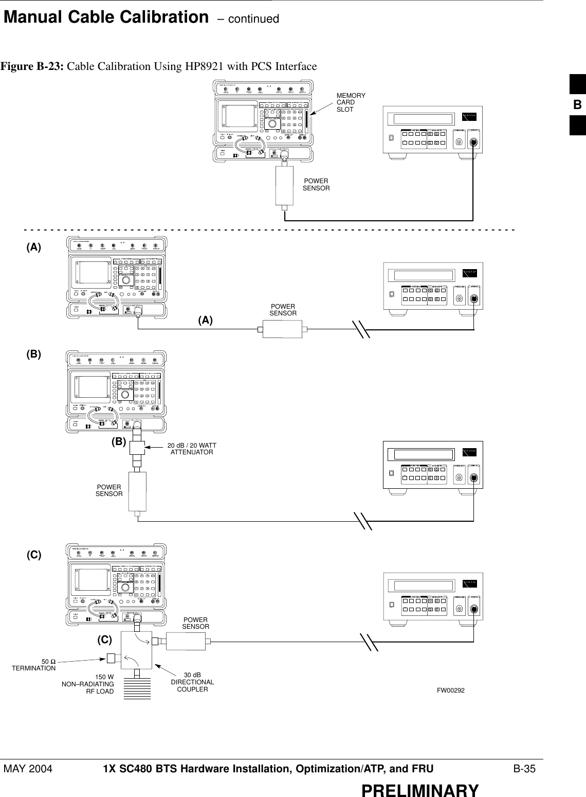
![Manual Cable Calibration B-32 1X SC480 BTS Hardware Installation, Optimization/ATP, and FRU MAY 2004PRELIMINARYCalibrating Test Cable SetupUsing HP PCS Interface(HP83236)Table B-23 covers the procedure to calibrate the test equipment using theHP8921 Cellular Communications Analyzer equipped with the HP83236PCS Interface.NOTE This calibration method must be executed with great care. Somelosses are measured close to the minimum limit of the powermeter sensor (–30 dBm).PrerequisitesEnsure the following prerequisites have been met before proceeding:STest equipment to be calibrated has been connected correctly for cablecalibration.STest equipment has been selected and calibrated.Table B-23: Calibrating Test Cable Setup (using the HP PCS Interface)Step ActionNOTEVerify that GPIB controller is turned off.1Insert HP83236 Manual Control System card into memory card slot.2Press the Preset pushbutton.3 Under Screen Controls, press the TESTS pushbutton to display the TESTS (Main Menu) screen.4Position the cursor at Select Procedure Location and select it. In the Choices selection box, selectCARD.5Position the cursor at Select Procedure Filename and select it. In the Choices selection box, selectMANUAL.6Position the cursor at RUN TEST and select it. HP must be in Control Mode Select YES.7If using HP83236A:Set channel number=<chan#>:– Position cursor at ChannelNumber and select it.– Enter the chan# using the numerickeypad; press [Enter] and thescreen will go blank.– When the screen reappears, thechan# will be displayed on thechannel number line.If using HP83236B:Set channel frequency:– Position cursor at Frequency Band and press Enter.– Select User Defined Frequency.– Go Back to Previous Menu.– Position the cursor to 83236 generator frequency andenter actual RX frequency.– Position the cursor to 83236 analyzer frequency andenter actual TX frequency.8Set RF Generator level:– Position the cursor at RF Generator Level and select it.– Enter –10 using the numeric keypad; press [Enter] and the screen will go blank.– When the screen reappears, the value –10 dBm will be displayed on the RF Generator Level line.. . . continued on next pageB](https://usermanual.wiki/Nokia-Solutions-and-Networks/T5EJ1.User-Manual-Part-4/User-Guide-430570-Page-58.png)
![Manual Cable Calibration – continuedMAY 2004 1X SC480 BTS Hardware Installation, Optimization/ATP, and FRU B-33PRELIMINARYTable B-23: Calibrating Test Cable Setup (using the HP PCS Interface)Step Action9Set the user fixed Attenuation Setting to 0 dBm:– Position cursor at Analyzer Attenuation and select it– Position cursor at User Fixed Atten Settings and select it.– Enter 0 (zero) using the numeric keypad and press [Enter].10 Select Back to Previous Menu.11 Record the HP83236 Generator Frequency Level:Record the HP83236B Generator Frequency Level:– Position cursor at Show Frequency and Level Details and select it.– Under HP83236 Frequencies and Levels, record the Generator Level.– Under HP83236B Frequencies and Levels, record the Generator Frequency Level (1850 – 1910MHz).– Position cursor at Prev Menu and select it.12 Click on Pause for Manual Measurement.13 Connect the power sensor directly to the RF OUT ONLY port of the PCS Interface.14 On the HP8921A, under To Screen, select CDMA GEN.15 Move the cursor to the Amplitude field and click on the Amplitude value.16 Increase the Amplitude value until the power meter reads 0 dBm ±0.2 dB.NOTEThe Amplitude value can be increased coarsely until 0 dBM is reached; then fine tune the amplitudeby adjusting the Increment Set to 0.1 dBm and targeting in on 0 dBm.17 Disconnect the power sensor from the RF OUT ONLY port of the PCS Interface.NOTEThe Power Meter sensor’s lower limit is –30 dBm. Thus, only components having losses ≤30 dBshould be measured using this method. For further accuracy, always re-zero the power meterbefore connecting the power sensor to the component being calibrated. After connecting thepower sensor to the component, record the calibrated loss immediately.18 Disconnect all components in the test setup and calibrate each one separately by connecting eachcomponent, one-at-a-time, between the RF OUT ONLY PORT and the power sensor. Record thecalibrated loss value displayed on the power meter.SExample: (A) Test Cable(s) = –1.4 dB(B) 20 dB Attenuator = –20.1 dB(B) Directional Coupler = –29.8 dB19 After all components are calibrated, reassemble all components together and calculate the total testsetup loss by adding up all the individual losses:SExample: Total test setup loss = –1.4 –29.8 –20.1 = –51.3 dB.This calculated value will be used in the next series of tests.20 Under Screen Controls press the TESTS button to display the TESTS (Main Menu) screen.. . . continued on next pageB](https://usermanual.wiki/Nokia-Solutions-and-Networks/T5EJ1.User-Manual-Part-4/User-Guide-430570-Page-59.png)
![Manual Cable Calibration – continued B-34 1X SC480 BTS Hardware Installation, Optimization/ATP, and FRU MAY 2004PRELIMINARYTable B-23: Calibrating Test Cable Setup (using the HP PCS Interface)Step Action21 Select Continue (K2).22 Select RF Generator Level and set to –119 dBm.23 Click on Pause for Manual Measurement.24 Verify the HP8921A Communication Analyzer/83203A CDMA interface setup is as follows (fieldsnot indicated remain at default):SVerify the GPIB (HP–IB) address:– under To Screen, select More– select IO CONFIG– Set HP–IB Adrs to 18– set Mode to Talk&LstnSVerify the HP8921A is displaying frequency (instead of RF channel)– Press the blue [SHIFT] button, then press the Screen Control [DUPLEX] button; this switches tothe CONFIG (CONFIGURE) screen.– Use the cursor control to set RF Display to Freq25 Refer toChapter 3 for assistance in setting the cable loss values into the LMF. B](https://usermanual.wiki/Nokia-Solutions-and-Networks/T5EJ1.User-Manual-Part-4/User-Guide-430570-Page-60.png)