Nokia Solutions and Networks T5EJ1 1X SC480 BTS Microcell Base Station Transmitter User Manual print instructions
Nokia Solutions and Networks 1X SC480 BTS Microcell Base Station Transmitter print instructions
Contents
- 1. User Manual Part 1
- 2. User Manual Part 2
- 3. User Manual Part 3
- 4. User Manual Part 4
User Manual Part 4

Basic Troubleshooting
MAY 2004 1X SC480 BTS Hardware Installation, Optimization/ATP, and FRU 11-1
PRELIMINARY
Overview
The information in this chapter addresses some of the scenarios likely to
be encountered by Customer Field Engineering (CFE) team members
while performing BTS optimization and acceptance testing. This
troubleshooting guide was created as an interim reference document for
use in the field. It provides “what to do if” basic troubleshooting
suggestions when the BTS equipment does not perform according to the
procedures documented in the manual.
Comments are consolidated from inputs provided by CFEs and
information gained from experience in Motorola labs and classrooms.
Table 11-1: Login Failure Troubleshooting Procedures
Step Action
1If the GLI LED is solid RED, it implies a hardware failure. Reset GLI by re-seating it. If this persists,
install GLI card in GLI slot and retry. A Red LED may also indicate no termination on an external
LAN connector (power entry compartment at rear of frame).
2Verify that the span line is disconnected at the Span I/O card. If the span is still connected, verify the
CBSC has disabled the BTS.
3Try to ‘ping’ the GLI.
4Verify the LMF is connected to the primary LAN (LAN A) at the LAN shelf below the CCP2 cage. If
LAN A is not the active LAN, force a LAN switch to LAN A by following the procedure in
Table 11-2.
5Verify the LMF was configured properly.
6If a Xircom parallel BNC LAN interface is being used, verify the BTS-LMF cable is RG-58 (flexible
black cable less than 2.5 feet in length).
7Verify the external LAN connectors are properly terminated (power entry compartment at rear of
frame).
8Verify a T-adapter is not used on LMF computer side connector when connected to the primary LAN
at the LAN shelf.
9Try connecting to the Ethernet Out port in the power entry compartment (rear of frame). Use a
TRB–to–BNC (triax–to–coax) adapter at the LAN connector for this connection.
10 Re-boot the LMF and retry.
11 Re-seat the GLI and retry
12 Verify GLI IP addresses are configured properly by following the procedure in Table 11-3.
11

Basic Troubleshooting – continued
11-2 1X SC480 BTS Hardware Installation, Optimization/ATP, and FRU MAY 2004
PRELIMINARY
Table 11-2: Force Ethernet LAN A to Active State as Primary LAN
Step Action
1If LAN A is not the active LAN, make certain all external LAN connectors are either terminated with
50Ω loads or cabled to another frame.
2If it has not already been done, connect the LMF computer to the stand–alone or starter frame, as
applicable (Table 6-6).
3If it has not already been done, start a GUI LMF session and log into the BTS on the active LAN
(Table 6-7).
4Remove the 50Ω termination from the LAN B IN connector in the power entry compartment at the
rear of the stand–alone or starter frame. The LMF session will become inactive.
5Disconnect the LMF computer from the LAN shelf LAN B connector and connect it to the LAN A
connector.
6If the LAN was successfully forced to an active state (the cards in any cage can be selected and
statused), proceed to step 13.
7With the 50Ω termination still removed from the LAN B IN connector, remove the 50Ω termination
from LAN B OUT connector. If more than one frame is connected to the LAN, remove the termination
from the last frame in the chain.
8If the LAN was successfully forced to an active state (the cards in any cage can be selected and
statused), proceed to step 13.
9With the 50Ω terminations still removed from LAN B, unseat each GLI card in each frame connected
to the LAN, until all are disconnected from the shelf backplanes.
10 Reseat each GLI card until all are reconnected.
11 Allow the GLIs to power up, and attempt to select and status cards in the CCP shelves. If LAN A is
active, proceed to step 13.
12 If LAN A is still not active, troubleshoot or continue troubleshooting following the procedures in 13.
13 Replace the 50Ω terminations removed from the LAN B IN and OUT connectors.
11

Basic Troubleshooting – continued
MAY 2004 1X SC480 BTS Hardware Installation, Optimization/ATP, and FRU 11-3
PRELIMINARY
Table 11-3: GLI IP Address Setting
Step Action
1If it has not previously been done, establish an MMI communication session with the GLI card as
described in Table 6-11.
2Enter the following command to display the IP address and subnet mask settings for the card:
config lg0 current
A response similar to the following will be displayed:
GLI3>config lg0 current
lg0: IP address is set to
DEFAULT (configured based on card location)
lg0: netmask is set to
DEFAULT (255.255.255.128)
3If the IP address setting response shows an IP address rather than “Default (configured based
on card location),” enter the following:
config lg0 ip default
A response similar to the following will be displayed:
GLI3>config lg0 ip default
_param_config_lg0_ip(): param_delete(): 0x00050001
lg0: ip address set to DEFAULT
4If the GLI subnet mask setting does not display as “DEFAULT (255.255.255.128),” set it to
default by entering the following command:
config lg0 netmask default
A response similar to the following will be displayed:
GLI3>config lg0 netmask default
_param_config_lg0_netmask(): param_delete(): 0x00050001
lg0: netmask set to DEFAULT
table continued on next page
11

Basic Troubleshooting – continued
11-4 1X SC480 BTS Hardware Installation, Optimization/ATP, and FRU MAY 2004
PRELIMINARY
Table 11-3: GLI IP Address Setting
Step Action
5Set the GLI route default to default by entering the following command:
config route default default
A response similar to the following will be displayed:
GLI3>config route default default
_esh_config_route_default(): param_delete(): 0x00050001
route: default gateway set to DEFAULT
NOTE
Changes to the settings will not take effect unless the GLI is reset.
6When changes are completed, close the MMI session, and reset the GLI card.
7Once the GLI is reset, re–establish MMI communication with it and issue the following command to
confirm its IP address and subnet mask settings:
config lg0 current
A response similar to the following will be displayed:
GLI3>config lg0 current
lg0: IP address is set to
DEFAULT (configured based on card location)
lg0: netmask is set to
DEFAULT (255.255.255.128)
11

Basic Troubleshooting – continued
MAY 2004 1X SC480 BTS Hardware Installation, Optimization/ATP, and FRU 11-5
PRELIMINARY
Cannot Communicate with
Power Meter
Table 11-4: Troubleshooting a Power Meter Communication Failure
Step Action
1Verify power meter is connected to LMF with GPIB adapter.
2Verify cable connections as specified in Chapter 4.
3Verify the GPIB address of the power meter is set to the same value displayed in the applicable GPIB
address box of the LMF Options window Test Equipment tab. Refer to Table 6-23 or Table 6-24 and
the Setting GPIB Addresses section of Appendix B for details.
4Verify the GPIB adapter DIP switch settings are correct. Refer to Test Equipment Preparation section
of Appendix F for details.
5Verify the GPIB adapter is not locked up. Under normal conditions, only 2 green LEDs must be ‘ON’
(Power and Ready). If any other LED is continuously ‘ON’, then cycle GPIB box power and retry.
6Verify the LMF computer COM1 port is not used by another application; for example, if a
HyperTerminal window is open for MMI, close it.
7 Reset all test equipment by clicking Util in the BTS menu bar and selecting Test Equipment > Reset
from the pull–down lists.
Cannot Communicate with
Communications System
Analyzer
Table 11-5: Troubleshooting a Communications System Analyzer Communication Failure
Step Action
1Verify analyzer is connected to LMF with GPIB adapter.
2Verify cable connections as specified in Chapter 4.
3Verify the analyzer GPIB address is set to the same value displayed in the applicable GPIB address
box of the LMF Options window Test Equipment tab. Refer to Table 6-23 or Table 6-24 and the
Setting GPIB Addresses section of Appendix B for details.
4Verify the GPIB adapter DIP switch settings are correct. Refer to Test Equipment Preparation section
of Appendix F for details.
5Verify the GPIB adapter is not locked up. Under normal conditions, only 2 green LEDs must be ‘ON’
(Power and Ready). If any other LED is continuously ‘ON’, then cycle GPIB box power and retry.
6Verify the LMF computer COM1 port is not used by another application; for example, if a
HyperTerminal window is open for MMI, close it.
7 Reset all test equipment by clicking Util in the BTS menu bar and selecting Test Equipment > Reset
from the pull–down lists.
11

Basic Troubleshooting – continued
11-6 1X SC480 BTS Hardware Installation, Optimization/ATP, and FRU MAY 2004
PRELIMINARY
Cannot Communicate with
Signal Generator
Table 11-6: Troubleshooting a Signal Generator Communication Failure
Step Action
1Verify signal generator is connected to LMF with GPIB adapter.
2Verify cable connections as specified in Chapter 4.
3Verify the signal generator GPIB address is set to the same value displayed in the applicable GPIB
address box of the LMF Options window Test Equipment tab. Refer to Table 6-23 or Table 6-24 and
the Setting GPIB Addresses section of Appendix B for details.
4Verify the GPIB adapter DIP switch settings are correct. Refer to Test Equipment Preparation section
of Appendix F for details.
5Verify the GPIB adapter is not locked up. Under normal conditions, only 2 green LEDs must be ‘ON’
(Power and Ready). If any other LED is continuously ‘ON’, then cycle GPIB box power and retry.
6Verify the LMF computer COM1 port is not used by another application; for example, if a
HyperTerminal window is open for MMI, close it.
7 Reset all test equipment by clicking Util in the BTS menu bar and selecting Test Equipment > Reset
from the pull–down lists.
Cannot Download
Table 11-7: Troubleshooting Code Download Failure
Step Action
1Verify T1 or E1 span is disconnected from the BTS.
2Verify LMF can communicate with the BTS devices using the LMF Status function.
3Communication with GLI must first be established before trying to communicate with any other BTS
device. GLI must be INS_ACT state (bright green).
4Verify the target card is physically present in the cage and powered-up.
5If the target card LED is solid RED, it implies hardware failure. Reset card by re-seating it. If LED
alarm persists, replace with same type of card from another slot and retry.
6Re-seat card and try again.
7If a BBX reports a failure message and is OOS_RAM, the code load was OK. Use the LMF Status
function to verify the load.
8If the download portion completes and the reset portion fails, reset the device by selecting the device
and Reset.
table continued on next page
11

Basic Troubleshooting – continued
MAY 2004 1X SC480 BTS Hardware Installation, Optimization/ATP, and FRU 11-7
PRELIMINARY
Table 11-7: Troubleshooting Code Download Failure
Step Action
9If a BBX or an MCC remains OOS_ROM (blue) after code download, use the LMF Device > Status
function to verify that the code load was accepted.
10 If the code load was accepted, use LMF Device > Download > Flash to load RAM code into flash
memory.
Cannot Download DATA to Any
Device (Card)
Table 11-8: Troubleshooting Data Download Failure
Step Action
1Re-seat card and repeat code and data load procedure.
2Verify the ROM and RAM code loads are of the same release by statusing the card. Refer to Download
the BTS section of Chapter 6 for more information.
Cannot ENABLE Device
Before a device can be enabled (placed in service), it must be in the
OOS_RAM state (yellow in LMF display) with data downloaded to the
device. The color of the device on the LMF changes to green once it is
enabled.
The four device states that can be displayed by the LMF are:
SEnabled (bright green, INS_ACT)
SStand–by (olive green, INS_SBY – redundant CSM and GLI only)
SDisabled (yellow, OOS_RAM)
SReset (blue, OOS_ROM)
Table 11-9: Troubleshooting Device Enable (INS) Failure
Step Action
1Re-seat card and repeat code and data load procedure.
2If CSA cannot be enabled, verify the CDF has correct latitude and longitude data for cell site location
and GPS sync.
3Ensure primary CSM is in INS_ACT (bright green) state.
NOTE
MCCs will not enable without the CSA being INS.
4Verify 19.6608 MHz CSA clock is present; MCCs will not enable without it.
table continued on next page
11

Basic Troubleshooting – continued
11-8 1X SC480 BTS Hardware Installation, Optimization/ATP, and FRU MAY 2004
PRELIMINARY
Table 11-9: Troubleshooting Device Enable (INS) Failure
Step Action
5BBXs should not be enabled for ATP tests.
6If MCCs give “invalid or no system time,” verify the CSA is enabled.
7Log out of the BTS, exit the LMF, restart the application, log into the BTS, and re–attempt
device–enable actions.
cCLPA Errors
Table 11-10: cCLPA Errors
Step Action
1If cCLPAs give continuous alarms, cycle power with the applicable DC PDA circuit breakers.
2Establish an MMI session with the cCLPA (Table 6-11), connecting the cable to the applicable MMI
port.
2a – Type alarms at the HyperTerminal window prompt and press Enter.
–– The resulting display may provide an indication of the problem.
2b – Call Field Support for further assistance.
11

MAY 2004 1X SC480 BTS Hardware Installation, Optimization/ATP, and FRU
PRELIMINARY
Appendix A: MCC–Data Only
Appendix Content
MCC–DO Tests A-1 . . . . . . . . . . . . . . . . . . . . . . . . . . . . . . . . . . . . . . . . . . . . . . . . .
MCC–DO Testing A-1 . . . . . . . . . . . . . . . . . . . . . . . . . . . . . . . . . . . . . . . . .
Prerequisites A-1 . . . . . . . . . . . . . . . . . . . . . . . . . . . . . . . . . . . . . . . . . . . . . .
Test Equipment A-1 . . . . . . . . . . . . . . . . . . . . . . . . . . . . . . . . . . . . . . . . . . .
MCC–DO Code Domain A-1 . . . . . . . . . . . . . . . . . . . . . . . . . . . . . . . . . . . .
MCC–DO TX Mask A-4 . . . . . . . . . . . . . . . . . . . . . . . . . . . . . . . . . . . . . . .
MCC–DO Pilot Time Offset A-6 . . . . . . . . . . . . . . . . . . . . . . . . . . . . . . . . .
MCC–DO Rho A-8 . . . . . . . . . . . . . . . . . . . . . . . . . . . . . . . . . . . . . . . . . . . .
MCC–DO Packet Error Rate A-9 . . . . . . . . . . . . . . . . . . . . . . . . . . . . . . . . .
PER Prerequisites A-9 . . . . . . . . . . . . . . . . . . . . . . . . . . . . . . . . . . . . . . . . .
A

Table of Contents – continued
1X SC480 BTS Hardware Installation, Optimization/ATP, and FRU MAY 2004
PRELIMINARY
Notes
A

MCC–DO Tests
MAY 2004 A-1
1X SC480 BTS Hardware Installation, Optimization/ATP, and FRU
PRELIMINARY
MCC–DO Testing
The tests in this appendix are provided for information
only. The tests contained herein are not proven, and
recommended equipment and equipment setup is not
provided.
IMPORTANT
*
The following acceptance tests evaluate different performance aspects of
the BTS with MCC–DO. This allows the CFE to select testing to meet
the specific requirements for individual maintenance and performance
verification situations.
The WinLMF must be version 2.16.4.0.04 or higher (with FR8000 –
EV–DO manual ATP test support).
Prerequisites
Before attempting to run any performance verification ATP tests, all
procedures outlined in previous Optimization chapters should have been
successfully completed. At a minimum, successful completion of all
BTS BLO calibration, and Bay Level Offset tests is recommended.
Test Equipment
Listed below are the recommended test equipment required to test
MCC–DO.
Signal Generator:
SAgilent E4432B, with options UN8/(008 for upgrade) and 201/(251
for upgrade)
SE4430BK–404 – CDMA2000–1xEV–DO signal studio software
OR
S Agilent E4438C, with options UN8/(008 for upgrade) and 201/(251
for upgrade)
SE4438CK–404 – CDMA2000–1xEV–DO signal studio software
Spectrum Analyzer:
SAgilent E4406A), with option B78 and Firmware version A.04.21
SE4406AU–204 – 1xEV–DO measurement personality
MCC–DO Code Domain
The code domain power test verifies the noise floor of a carrier keyed up
at a specific frequency per the CDF file.
Code domain power is the power in each code channel of a CDMA
Channel. The CDMA time reference used in the code domain power test
is derived from the Pilot Channel and is used as the reference for
demodulation of all other code channels. This test verifies that
orthogonality is maintained between the code channels. When transmit
diversity is enabled, this test also verifies that time alignment is also
maintained.
A

MCC–DO Tests – continued
PRELIMINARY
1X SC480 BTS Hardware Installation, Optimization/ATP, and FRU MAY 2004
A-2
Follow the procedure in Table A-1 to test the MCC–DO Code Domain
Power.
Table A-1: Procedure to Test MCC–DO Code Domain Power
Step Action
1Click the BBX(s) on DO carrier to be tested.
2On the menu, click the EvDO Tests > TX>Start Manual Tx ATP.
3Select the appropriate carrier from the Sector/Carrier list.
4Click the OK button.
A status report window is displayed.
5Test tesults are displayed in the window.
6Connect an MMI cable to the MCC–DO card.
7Open a HyperTerminal application.
8Open the COM to the MCC–DO MMI. Set parameters as follows:
SBits per second: 9600
SData bits: 8
SParity: None
SStop bits: 1
SFlow control: None
9When the login prompt appears, enter login mmi.
10 When MMI> appears, type in the following command:
set_sc <modem number> <sector number> <channel> <PN offset>
where:
S<modem number> is the modem on MCC–DO card to be tested
S<sector number> is the sector number of the appropriate BBX (according to carrier selected in
LMF)
S<channel> is the appropriate channel (according to carrier selected in LMF) in the hexadecimal
format 0xHHHH or NNNN format (normal decimal)
S<PN offset> is set to 0 (zero)
11 Enable the modem on MCC–DO card by entering the following command:
enable <modem number>
where:
S<modem number> is the modem selected in step 10.
table continued on next page
A

MCC–DO Tests – continued
MAY 2004 A-3
1X SC480 BTS Hardware Installation, Optimization/ATP, and FRU
PRELIMINARY
Table A-1: Procedure to Test MCC–DO Code Domain Power
Step Action
12 To generate a pattern, enter the following command:
fl_pattern 3
13 On the Agilent E4406, set the Code Domain:
SPress Measure button
SPress More button until Code Domain option is displayed
SSelect Code Domain
SPress Meas Setup button, then press Meas Interval, enter 3.
SPress Meas Control button, then press Measure to set it to Cont
SPress Meas Control button
SSet Channel Type to MAC
SPress More button until Trig Source option is displayed
SPress Trig Source key and select Ext Rear option
SPress More button until Advanced option is displayed
SSelect Advanced option
SIf Chip Rate option is set to a value different than 1.228800, select Chip Rate and set it to
1.228800
SSelect Active Set Th option to a value calculated using the following formula:
–xcvr_gain – cable_loss – 2dB
SPress Display button and set the I/Q Combined Power Bar to On
SPress Display button, press Code Order button, select Hadamard option
STo set appropriate frequency value, press Frequency and enter the value calculated according to the
following formula:
–<tx_base_band_value> + 0.05*<chan_no> [MHz]
14 Read the value of the power for each MAC channel.
15 Note the Max Inactive Ch value. The Max Inactive Ch value is –31dB or lower.
A

MCC–DO Tests – continued
PRELIMINARY
1X SC480 BTS Hardware Installation, Optimization/ATP, and FRU MAY 2004
A-4
MCC–DO TX Mask
Follow the procedure in Table A-2 to test the MCC–DO TX Mask.
Table A-2:Procedure to Test the MCC–DO TX Mask
Step Action
1Click the BBX(s) on DO carrier to be tested.
2On the menu, click the EvDO Tests > TX>Start Manual Tx ATP.
3Select the appropriate carrier from the Sector/Carrier list.
4Click the OK button.
A status report window is displayed.
5Connect test equipment as the instructions are displayed.
6Connect an MMI cable to the MCC–DO card.
7Open a HyperTerminal application.
8Open the COM to the MCC–DO MMI. Set parameters as follows:
SBits per second: 9600
SData bits: 8
SParity: None
SStop bits: 1
SFlow control: None
9When the login prompt appears, enter login mmi.
10 When MMI> appears, type in the following command:
set_sc <modem number> <sector number> <channel> <PN offset>
where:
S<modem number> is the modem on MCC–DO card to be tested
S<sector number> is the sector number of the appropriate BBX (according to carrier selected in
LMF)
S<channel> is the appropriate channel (according to carrier selected in LMF) in the hexadecimal
format 0xHHHH or NNNN format (normal decimal).
S<PN offset> is set to 0 (zero)
11 Enable the modem on MCC–DO card by entering the following command:
enable <modem number>
where:
S<modem number> is the modem selected in step 10.
table continued on next page
A

MCC–DO Tests – continued
MAY 2004 A-5
1X SC480 BTS Hardware Installation, Optimization/ATP, and FRU
PRELIMINARY
Table A-2:Procedure to Test the MCC–DO TX Mask
Step Action
12 To generate a pattern, enter the following command:
fl_pattern 3
13 On Agilent E4406, set Spectrum (Freq Domain) measurement as follows:
SPress Measure button
SPress More button until Spectrum (Freq Domain) option is displayed
SSelect Spectrum option
SPress SPAN key to set its value to 4 [MHz]
STo set the frequency value. press Frequency and enter the value calculated as follows:
–<tx_base_band_value> + 0.05*<chan_no> [MHz]
14 Use the formula from step 13 to calculate the four frequencies to measure the Power.
Scheck_point_1 = freq – 750 [kHz]
Scheck_point_2 = freq + 750[kHz]
Scheck_point_3 = freq – 1980 [kHz]
Scheck_point_4 = freq + 1980 [kHz]
15 Press MARKER key:
SSelect 1, 2, 3, or 4 (frequency points)
SPress FUNCTION key and select Off option
SPress TRACE key and select Spectrum option
SPress NORMAL key
SUse the numeric keypad to enter the calculated frequency, assigning the proper unit.
SNote the Power value of marker
SRepeat step for all calculated frequency checkpoints
The check point values are as follows:
SCheck_point_1 > –40 dBm
SCheck_point_2 > –40 dBm
SCheck_point_3 > –60 dBm
SCheck_ point_4 > –60 dBm
A

MCC–DO Tests – continued
PRELIMINARY
1X SC480 BTS Hardware Installation, Optimization/ATP, and FRU MAY 2004
A-6
MCC–DO Pilot Time Offset
The pilot time offset test verifies the transmitted pilot channel element
pilot time offset of a carrier keyed up at a specific frequency per the CDF
file.
The calibrated communications test set measures the pilot time offset in
microseconds, verifying that the result is within 3 microseconds (10
microseconds for JCDMA systems) of the target pilot time offset (zero
microseconds).
Pilot time is defined as the estimate of CDMA System Time derived
from observation of the pilot signal at the base station RF output port.
Pilot time alignment error is the difference between the measured pilot
time and the expected time, taking into account CDMA System Time
and pilot offset.
Follow the procedure in Table A-3 to test the MCC–DO Pilot Time
Offset.
Table A-3: Procedure to Test MCC–DO Pilot Time Offset
Step Action
1Click the BBX(s) on DO carrier to be tested.
2On the menu, click the EvDO Tests > TX>Start Manual Tx ATP.
3Select the appropriate carrier from the Sector/Carrier list.
4Click the OK button.
A status report window is displayed. Test results are displayed in the window.
5Connect an MMI cable to the MCC–DO card.
6Open a HyperTerminal application.
7Open the COM to the MCC–DO MMI. Set parameters as follows:
SBits per second: 9600
SData bits: 8
SParity: None
SStop bits: 1
SFlow control: None
8When the login prompt appears, enter login mmi.
table continued on next page
A

MCC–DO Tests – continued
MAY 2004 A-7
1X SC480 BTS Hardware Installation, Optimization/ATP, and FRU
PRELIMINARY
Table A-3: Procedure to Test MCC–DO Pilot Time Offset
Step Action
9 When MMI> appears, type in the following command:
set_sc <modem number> <sector number> <channel> <PN offset>
where:
S<modem number> is the modem on MCC–DO card to be tested
S<sector number> is the sector number of the appropriate BBX (according to carrier selected in
LMF)
S<channel> is the appropriate channel (according to carrier selected in LMF) in the hexadecimal
format 0xHHHH or NNNN format (normal decimal).
S<PN offset> is set to 0 (zero)
10 Enable the modem on MCC–DO card by entering the following command:
enable <modem number>
where:
S<modem number> is the modem selected in step 10.
11 To generate a pattern, enter the following command:
fl_pattern 3
12 On the Agilent E4406, set the Mod Accuracy (composite Rho) measurement:
SPress Measure button
SPress More button until Mod Accuracy (composite Rho) option is displayed
SSelect Mod Accuracy (composite Rho)
SPress Meas Setup button
SPress More button until Trig Source option is displayed
SPress Trig Source key and select Ext Rear option
SPress More button until Advanced option is displayed
SSelect Advanced option
SIf Chip Rate option is set to a value different than 1.228800, select Chip Rate and set it to
1.228800
SSelect Active Set Th option to a value calculated using the following formula:
–xcvr_gain – cable_loss – 2dB
STo set appropriate frequency value, press Frequency and enter the value calculated according to the
following formula:
–<tx_base_band_value> + 0.05*<chan_no> [MHz]
13 Read the value of thePilot Offset. The Pilot Offset is less than 3 microseconds
A

MCC–DO Tests – continued
PRELIMINARY
1X SC480 BTS Hardware Installation, Optimization/ATP, and FRU MAY 2004
A-8
MCC–DO Rho
The Rho test verifies the transmitted pilot channel element digital
waveform quality of the carrier keyed up at a specific frequency per the
CDF file.
Waveform quality is measured by determining the normalized correlated
power between the actual waveform and the ideal waveform.
Follow the procedure in Table A-4 to test the MCC–DO Rho.
Table A-4: Procedure to Test MCC–DO Rho
Step Action
1Click the BBX(s) on DO carrier to be tested.
2On the menu, click the EvDO Tests > TX>Start Manual Tx ATP.
3Select the appropriate carrier from the Sector/Carrier list.
4Click the OK button.
A status report window is displayed. Test results are displayed in the window.
5Connect an MMI cable to the MCC–DO card.
6Open a HyperTerminal application.
7Open the COM to the MCC–DO MMI. Set parameters as follows:
SBits per second: 9600
SData bits: 8
SParity: None
SStop bits: 1
SFlow control: None
8When the login prompt appears, enter login mmi.
9 When MMI> appears, type in the following command:
set_sc <modem number> <sector number> <channel> <PN offset>
where:
S<modem number> is the modem on MCC–DO card to be tested
S<sector number> is the sector number of the appropriate BBX (according to carrier selected in
LMF)
S<channel> is the appropriate channel (according to carrier selected in LMF) in the hexadecimal
format 0xHHHH or NNNN format (normal decimal).
S<PN offset> is set to 0 (zero)
table continued on next page
A

MCC–DO Tests – continued
MAY 2004 A-9
1X SC480 BTS Hardware Installation, Optimization/ATP, and FRU
PRELIMINARY
Table A-4: Procedure to Test MCC–DO Rho
Step Action
10 Enable the modem on MCC–DO card by entering the following command:
enable <modem number>
where:
S<modem number> is the modem selected in step 10.
11 To generate a pattern, enter the following command:
fl_pattern 3
12 On the Agilent E4406, set the Mod Accuracy (composite Rho) measurement:
SPress Measure button
SPress More button until Mod Accuracy (composite Rho) option is displayed
SSelect Mod Accuracy (composite Rho)
SPress Meas Setup button
SPress More button until Trig Source option is displayed
SPress Trig Source key and select Ext Rear option
SPress More button until Advanced option is displayed
SSelect Advanced option
SIf Chip Rate option is set to a value different than 1.228800, select Chip Rate and set it to
1.228800
SSelect Active Set Th option to a value calculated using the following formula:
–xcvr_gain – cable_loss – 2dB
STo set appropriate frequency value, press Frequency and enter the value calculated according to the
following formula:
–<tx_base_band_value> + 0.05*<chan_no> [MHz]
13 Read the value of the Rho. Rho normalized cross coefficient ( ò ) is greater than 0.912
MCC–DO Packet Error Rate
The PER test verifies PER (Packet Error Rate) of traffic channels of an
XCVR carrier keyed up at a specific frequency per the current CDF file.
The XCVR is keyed to generate a CDMA carrier (with pilot channel
element only) of the correct level.
The calibrated communications test set measures the all zero long code
and verifies that the PER is not greater than 1 percent. A total number of
packets to be received is dependent on Rate Set chosen.
PER Prerequisites
To perform the following test, the Agilent E4432B Signal Generator
must have the following installed:
A

MCC–DO Tests – continued
PRELIMINARY
1X SC480 BTS Hardware Installation, Optimization/ATP, and FRU MAY 2004
A-10
SAgilent Signal Studio – 1xEV Reverse Link” (requires installation of
”Agilent IO Libraries” application)
SAgilent E4432B Signal Generator with option 404
Follow the procedure in Table A-5 to test the MCC–DO Packet Error
Rate.
Table A-5: Procedure to Test MCC–DO Packet Error Rate
Step Action
1Click the BBX(s) on DO carrier to be tested.
2On the menu, click the EvDO Tests > TX>Start Manual Tx ATP.
3Select the appropriate carrier from the Sector/Carrier list.
4Click the OK button.
A status report window is displayed. Test results are displayed in the window.
5Connect the lap top computer to the Agilent E4432B Signal Generator and run the Agilent Signal
Studio – 1x EV Reverse Link application.
table continued on next page
A

MCC–DO Tests – continued
MAY 2004 A-11
1X SC480 BTS Hardware Installation, Optimization/ATP, and FRU
PRELIMINARY
Table A-5: Procedure to Test MCC–DO Packet Error Rate
Step Action
6Enter the following parameters for signal generation.
Channel Configuration:
SRRI Channel – checked RRI Bits – 1
SDRC Channel – checked Rel. gain (dB) – 3
SACK Channel – checked Rel. gain (dB) – 0
SData Channel – checked Rel. gain (dB) – 3.75
SData Channel encoder active – checked
SData Channel Data rate – 9.6 kbps
SData Channel bit stream – PN15
SI Mask – 3FF80000000
SQ Mask – 3FF00000001
Signal Generation:
SOversampling ratio – 4
SFilter Type – IS 95 Std
SMirror Spectrum – unchecked
ESG Configuration:
SFrequency – calculated according to the formula: <rx_base_band_value> + 0,05 * <chan_no>
[MHz]
SAmplitude – depending on attenuation applied – overall signal value should be –122 [dBm]
SSampling rate 4.1952 [MHz]
SReconstruction filter 2.5 [MHz]
SRF Blanking – unchecked
SInternal Reference
S+ Mkrs
7 Press Time Slot Setup button and set the following parameters:
ACK Channel
SActive – All On
SData – 0s
DRC Channel
SActive – All On
SData – F (1111)
SCover – 1
8 Press DOWNLOAD button on the ”Agilent Signal Studio – 1xEV Reverse Link” application.
table continued on next page
A

MCC–DO Tests – continued
PRELIMINARY
1X SC480 BTS Hardware Installation, Optimization/ATP, and FRU MAY 2004
A-12
Table A-5: Procedure to Test MCC–DO Packet Error Rate
Step Action
9Connect an MMI cable to the MCC–DO card.
10 Open a HyperTerminal application.
11 Open the COM to the MCC–DO MMI. Set parameters as follows:
SBits per second: 9600
SData bits: 8
SParity: None
SStop bits: 1
SFlow control: None
12 When the login prompt appears, enter login mmi.
13 When MMI> appears, type in the following command:
set_sc <modem number> <sector number> <channel> <PN offset>
where:
S<modem number> is the modem on MCC–DO card to be tested
S<sector number> is the sector number of the appropriate BBX (according to carrier selected in
LMF)
S<channel> is the appropriate channel (according to carrier selected in LMF) in the hexadecimal
format 0xHHHH or NNNN format (normal decimal).
S<PN offset> is set to 0 (zero)
table continued on next page
A

MCC–DO Tests – continued
MAY 2004 A-13
1X SC480 BTS Hardware Installation, Optimization/ATP, and FRU
PRELIMINARY
Table A-5: Procedure to Test MCC–DO Packet Error Rate
Step Action
14 Enter the command to receive the PER measurements results:
rl_test 1 60 dflt dflt dflt dflt dflt dflt dflt dflt dflt dflt dflt dflt dflt dflt
this will set the MCC–DO to measure the PER with following parameters:
SPerform PER Test at 9.6 KBPS
SDuration 60 seconds
SDataOffsetNominal dflt=0dB
SDataOffset9k6 dflt=0dB
SDataOffset19k2 dflt=0dB
SDataOffset38k4 dflt=0dB
SDataOffset76k8 dflt=0dB
SDataOffset153k6 dflt=0dB
SMacIndex dflt=5
SFrameOffset dflt=0
SDRCGating dflt=0 Continuous transmission
SDRCLength dflt = 0
SDRCCover dflt = 1
SUATI dflt = 0x1234ABCD
SAckChannelGain dflt=0dB
SDRCChannelGain dflt=3dB
15 Read the results (after 1 minute) and calculate the PER value from the MCC–DO mmi result screen:
Compute PER using the outcome of the rl_test
PER = (expect–total+invalid) /expect
Example output:
Reverse Link Test has completed
Reverse Link Test OK MODEM#1
pattern = 1 (9.6 kbps)
expect = xxx
total = xxx
invalid = xxx
16 Receiver sensitivity is below –121.2 dBm at a signal rate of 9.6 kbps.
Read the value of the PER. PER is less than 0.01 (1%)
A

MCC–DO Tests – continued
PRELIMINARY
1X SC480 BTS Hardware Installation, Optimization/ATP, and FRU MAY 2004
A-14
Notes
A

MAY 2004 1X SC480 BTS Hardware Installation, Optimization/ATP, and FRU
PRELIMINARY
Appendix B: Test Equipment Preparation
Appendix Content
Test Equipment Preparation B-1 . . . . . . . . . . . . . . . . . . . . . . . . . . . . . . . . . . . . . . . .
Purpose B-1 . . . . . . . . . . . . . . . . . . . . . . . . . . . . . . . . . . . . . . . . . . . . . . . . .
Agilent R7495A Test Equipment Setup B-2 . . . . . . . . . . . . . . . . . . . . . . . .
Verifying and Setting GPIB Addresses B-5 . . . . . . . . . . . . . . . . . . . . . . . . . . . . . . . .
Agilent E4406A Transmitter Tester GPIB Address B-5 . . . . . . . . . . . . . . . .
Agilent E4432B Signal Generator GPIB Address B-6 . . . . . . . . . . . . . . . . .
Advantest R3267 Spectrum Analyzer GPIB Address B-7 . . . . . . . . . . . . . .
Advantest R3562 Signal Generator GPIB Address B-9 . . . . . . . . . . . . . . . .
Agilent 8935 Series E6380 (formerly HP 8935) Test Set GPIB Address B-9
Hewlett Packard HP8921A and HP83236A/B GPIB Address B-11 . . . . . . .
Advantest R3465 Communications Test Set GPIB Address B-12 . . . . . . . . .
Motorola CyberTest GPIB Address B-13 . . . . . . . . . . . . . . . . . . . . . . . . . . . .
HP 437 Power Meter GPIB Address B-14 . . . . . . . . . . . . . . . . . . . . . . . . . . .
Gigatronics 8541C Power Meter GPIB Address B-15 . . . . . . . . . . . . . . . . . .
RS232 GPIB Interface Adapter B-16 . . . . . . . . . . . . . . . . . . . . . . . . . . . . . . .
Test Equipment Connection, Testing, and Control B-17 . . . . . . . . . . . . . . . . . . . . . . .
Inter–unit Connection, Testing, and Control Settings B-17 . . . . . . . . . . . . . .
HP 8921A with PCS Interface Test Equipment Connections B-17 . . . . . . . .
HP 8921A with PCS Interface System Connectivity Test B-21 . . . . . . . . . . .
Pretest Setup for HP 8921A B-21 . . . . . . . . . . . . . . . . . . . . . . . . . . . . . . . . . .
Pretest Setup for Agilent 8935 B-22 . . . . . . . . . . . . . . . . . . . . . . . . . . . . . . . .
Advantest R3465 Connection B-22 . . . . . . . . . . . . . . . . . . . . . . . . . . . . . . . .
R3465 GPIB Clock Set–up B-24 . . . . . . . . . . . . . . . . . . . . . . . . . . . . . . . . . .
Pretest Setup for Advantest R3465 B-25 . . . . . . . . . . . . . . . . . . . . . . . . . . . .
Agilent 8932/E4432B Test Equipment Interconnection B-25 . . . . . . . . . . . .
Agilent E4406A/E4432B Test Equipment Interconnection B-26 . . . . . . . . .
Advantest R3267/R3562 Test Equipment Interconnection B-27 . . . . . . . . . .
Equipment Calibration B-28 . . . . . . . . . . . . . . . . . . . . . . . . . . . . . . . . . . . . . . . . . . . .
Calibration Without the LMF B-28 . . . . . . . . . . . . . . . . . . . . . . . . . . . . . . . .
Agilent E4406A Transmitter Tester Self–alignment (Calibration) B-28 . . . .
Calibrating HP 437 Power Meter B-29 . . . . . . . . . . . . . . . . . . . . . . . . . . . . .
Calibrating Gigatronics 8541C Power Meter B-31 . . . . . . . . . . . . . . . . . . . .
Manual Cable Calibration B-32 . . . . . . . . . . . . . . . . . . . . . . . . . . . . . . . . . . . . . . . . . .
Calibrating Test Cable Setup
Using HP PCS Interface (HP83236) B-32 . . . . . . . . . . . . . . . . . . . . . . . . . . .
Calibrating Test Cable Setup Using Advantest R3465 B-36 . . . . . . . . . . . . .
B

Table of Contents – continued
1X SC480 BTS Hardware Installation, Optimization/ATP, and FRU MAY 2004
PRELIMINARY
Notes
B

Test Equipment Preparation
MAY 2004 1X SC480 BTS Hardware Installation, Optimization/ATP, and FRU B-1
PRELIMINARY
Purpose
This appendix provides information on pre–testing set–up for the
following test equipment items (not required for the Cybertest test set):
SAgilent E7495A test equipment setup
SAgilent E4406A transmitter test set
SAgilent E4432B signal generator
SAdvantest R3267 spectrum analyzer
SAdvantest R3562 signal generator
SAgilent 8935 analyzer (formerly HP 8935)
SHP 8921 with PCS interface analyzer
SAdvantest R3465 analyzer
SMotorola CyberTest
SHP 437 power meter
SGigatronics 8541C power meter
SGPIB adapter
Pre–testing set–up information covered includes verification and setting
GPIB addresses, inter–unit cabling, connectivity testing, pre–test control
settings, and equipment calibration for items which are not calibrated
with the Calibrate Test Equipment function of the LMF.
The following procedures cover verification and changing GPIB
addresses for the various items of CDMA test equipment supported by
the LMF.
B

Test Equipment Preparation – continued
B-2 1X SC480 BTS Hardware Installation, Optimization/ATP, and FRU MAY 2004
PRELIMINARY
Agilent R7495A Test Equipment
Setup
This test equipment requires a warm-up period of at least 30 minutes
before BTS testing or calibration begins.
Using the Agilent E7495A with the LMF
The Agilent E7495A does not require the use of the 19MHz frequency
reference; if connected, it will be ignored. The Even Sec SYNC
connection is required.
The Agilent E7495A signal generator is only calibrated down to –80db.
In order to achieve accurate FER testing, be sure the RX setup includes
at least 40db of attenuation. This will ensure the signal generator will
output sufficient power to operate in the calibrated range.
Set the IP Address as described in Table B-1.
Table B-1: Set IP Address on Agilent E7495A test set
nStep Action
1Use the System Button > Controls >IPAdmin to set an IP address on the E7495A as 128.0.0.49,
and Netmask to 255.255.255.128.
Connections
It is recommended that you use a hub with BNC and RJ–45 connections.
[Suggested models: Netgear model EN104 (4 port) or EN108 (8 port).
Do NOT use model numbers ending with “TP”; those have no BNC
connectors.]
The LMF will connect to the hub which in turn is connected to the BTS
and to the Agilent E7495A.
Agilent E7495A to Hub – This is an Ethernet cable, RJ–45 to RJ–45.
LMF to Hub – Use one of the following cables to connect the LMF to
the Hub:
– Ethernet cable, RJ–45 to RJ–45 (be sure that the LAN card is set for
either AUTO or to use the RJ–45 only).
– Coax cable between LAN card and Hub. (Use a “T” on the hub and
connect a cable between the other end of the “T” and the BTS LAN
connection).
Hub to BTS – Use BNC “T” connector on the hub. [If your hub doesn’t
have BNC ports, use a BNC to UTP adapter.]
B

Test Equipment Preparation – continued
MAY 2004 1X SC480 BTS Hardware Installation, Optimization/ATP, and FRU B-3
PRELIMINARY
Detecting Test Equipment
Check that no other equipment is connected to the LMF. Agilent
equipment must be connected to the LAN to detect it. Then perform the
procedures described in Table B-2.
Table B-2: Detecting Agilent E7495A Test Equipment
nStep Action
1Click the Tools Menu.
2 Choose Options.
3 Check Agilent E7495A option in non–GPIB Test Equipment and enter its IP number.
4 Click Apply and wait a moment.
5 Click Dismiss.
Power Sensor Calibration
Table B-3 describes the E7495A Power Sensor Calibration.
Table B-3: E7495A Power Sensor Calibration
nStep Action
1Display the power meter screen.
2Zero the power meter. Make sure you are connected as shown in Figure B-1.
– Press the Zero softkey.
– Press the Continue softkey.
3Calibrate the power meter:
– Press Ref CF.
– Enter the reference cal factor, reading it off the label on the power sensor head.
– Press Calibrate.
– Connect the power sensor (see Figure B-2).
– Press Continue.
– Press Cal Factor.
– Enter the cal factor from the label on the power sensor head. Select a cal factor that’s within
the operating frequency of the base station.
B
Test Equipment Preparation – continued
B-4 1X SC480 BTS Hardware Installation, Optimization/ATP, and FRU MAY 2004
PRELIMINARY
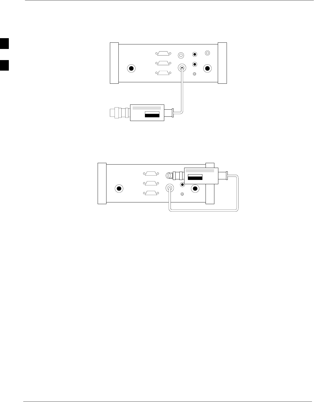
Figure B-1: Agilent E7495A Pre–Power Sensor Calibration Connection
Use only
Agilent supplied
power adapter
GPS
GPIO
Serial 1
Serial 2
Power REF
50 MHz
Sensor
Ext Ref
In
Even Second
Sync In
Antenna
Port 1
RF Out / SWR
Port 2
RF In
POWER SENSOR
NOT CONNECTED
Figure B-2: Agilent E7495A Power Sensor Calibration Connection
Use only
Agilent supplied
power adapter
GPS
GPIO
Serial 1
Serial 2
Power REF
50 MHz
Sensor
Ext Ref
In
Even Second
Sync In
Antenna
Port 1
RF Out / SWR
Port 2
RF In
POWER SENSOR
CONNECTED
Cable Calibration
Follow the directions in the WinLMF program to calibrate cables.
– Calibrate the short cable (see Figure 6-12 or Figure 6-13) and two
10 dB pads to get a base line and then calibrate the TX and RX
setup. Since you need at least 40 dB of loss when doing the FER
test, the setup for RX is the same as TX.
ATP Setup
TX Path Calibration setup is shown in Test Equipment Setup (see
Figure 6-17 through Figure 6-20).
B
Verifying and Setting GPIB Addresses
MAY 2004 1X SC480 BTS Hardware Installation, Optimization/ATP, and FRU B-5
PRELIMINARY
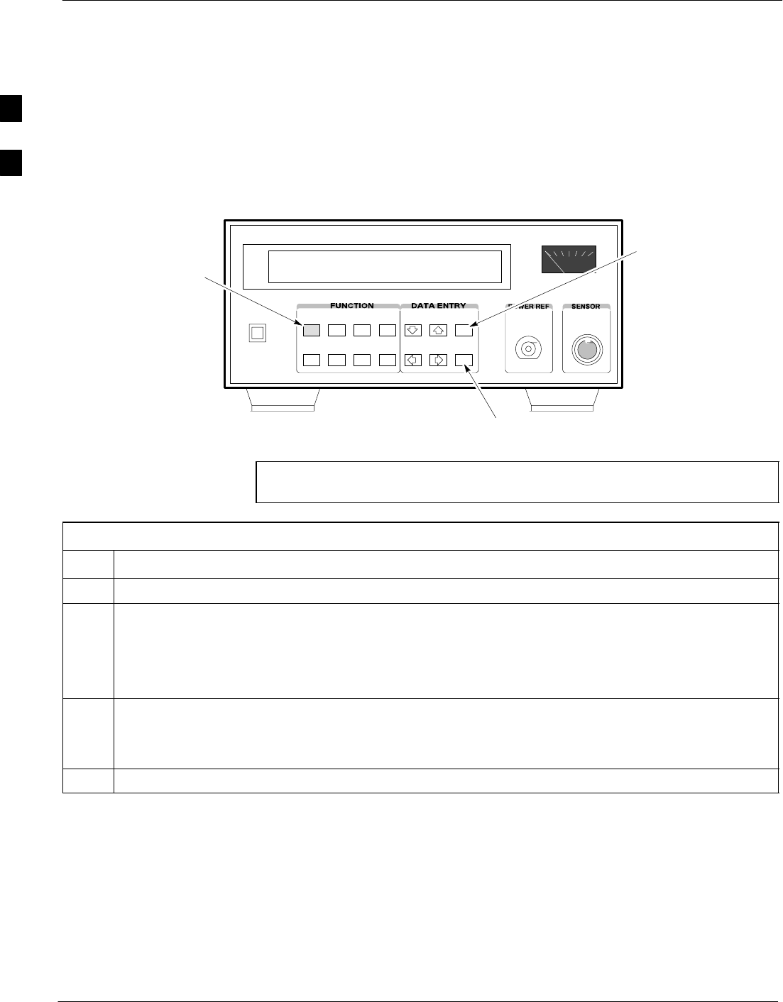
Agilent E4406A Transmitter
Tester GPIB Address
Refer to Figure B-3 and follow the procedure in Table B-4 to verify and,
if necessary, change the Agilent E4406A GPIB address.
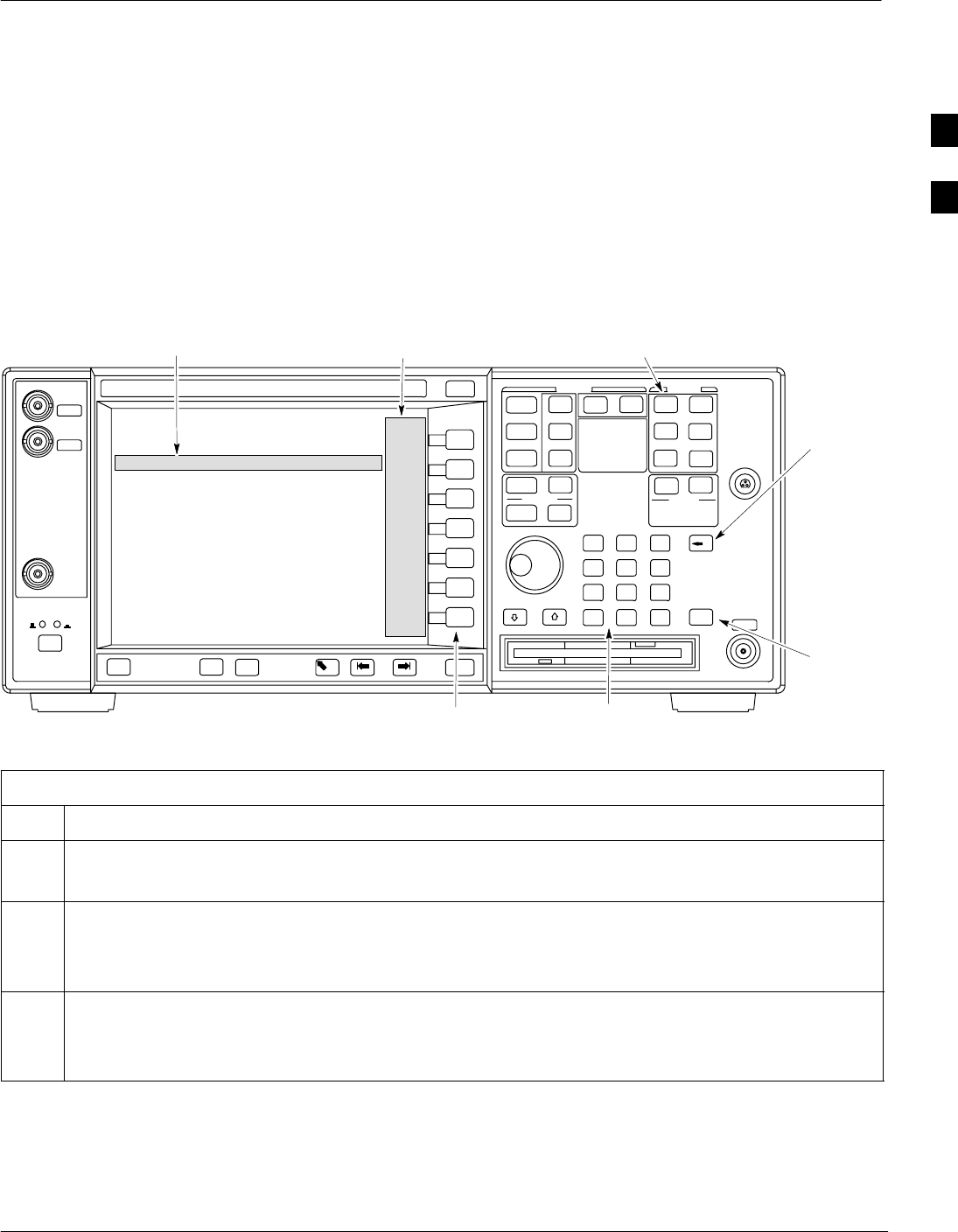
Figure B-3: Setting Agilent E4406A GPIB Address
System Key
Bk Sp Key
Enter Key
Data Entry KeypadSoftkey Buttons
Softkey Label Display AreaActive Function Area
ti-CDMA-WP-00085-v01-ildoc-ftw
Table B-4: Verify and Change Agilent E4406A GPIB Address
Step Action
1In the SYSTEM section of the instrument front panel, press the System key.
– The softkey labels displayed on the right side of the instrument screen will change.
2Press the Config I/O softkey button to the right of the instrument screen.
– The softkey labels will change.
– The current instrument GPIB address will be displayed below the GPIB Address softkey label.
3If the current GPIB address is not set to 18, perform the following to change it:
3a Press the GPIB Address softkey button. In the on–screen Active Function Area, GPIB Address will
be displayed followed by the current GPIB address.
. . . continued on next page
B
Verifying and Setting GPIB Addresses – continued
B-6 1X SC480 BTS Hardware Installation, Optimization/ATP, and FRU MAY 2004
PRELIMINARY
Table B-4: Verify and Change Agilent E4406A GPIB Address
Step Action
3b On front panel Data Entry keypad, enter the communications system analyzer GPIB address of 18.
– The GPIB Address label will change to Enter.
– Characters typed with the keypad will replace the current GPIB address in the Active Function
Area.
NOTE
To correct an entry, press Bk Sp key to delete one character at a time.
3c Press the Enter softkey button or the keypad Enter key to set the new GPIB address.
– The Config I/O softkey labels will reappear.
– The new GPIB address will be displayed under the GPIB Address softkey label.
Agilent E4432B Signal
Generator GPIB Address
Refer to Figure B-4 and follow the procedure in Table B-5 to verify and,
if necessary, change the Agilent E4432B GPIB address.
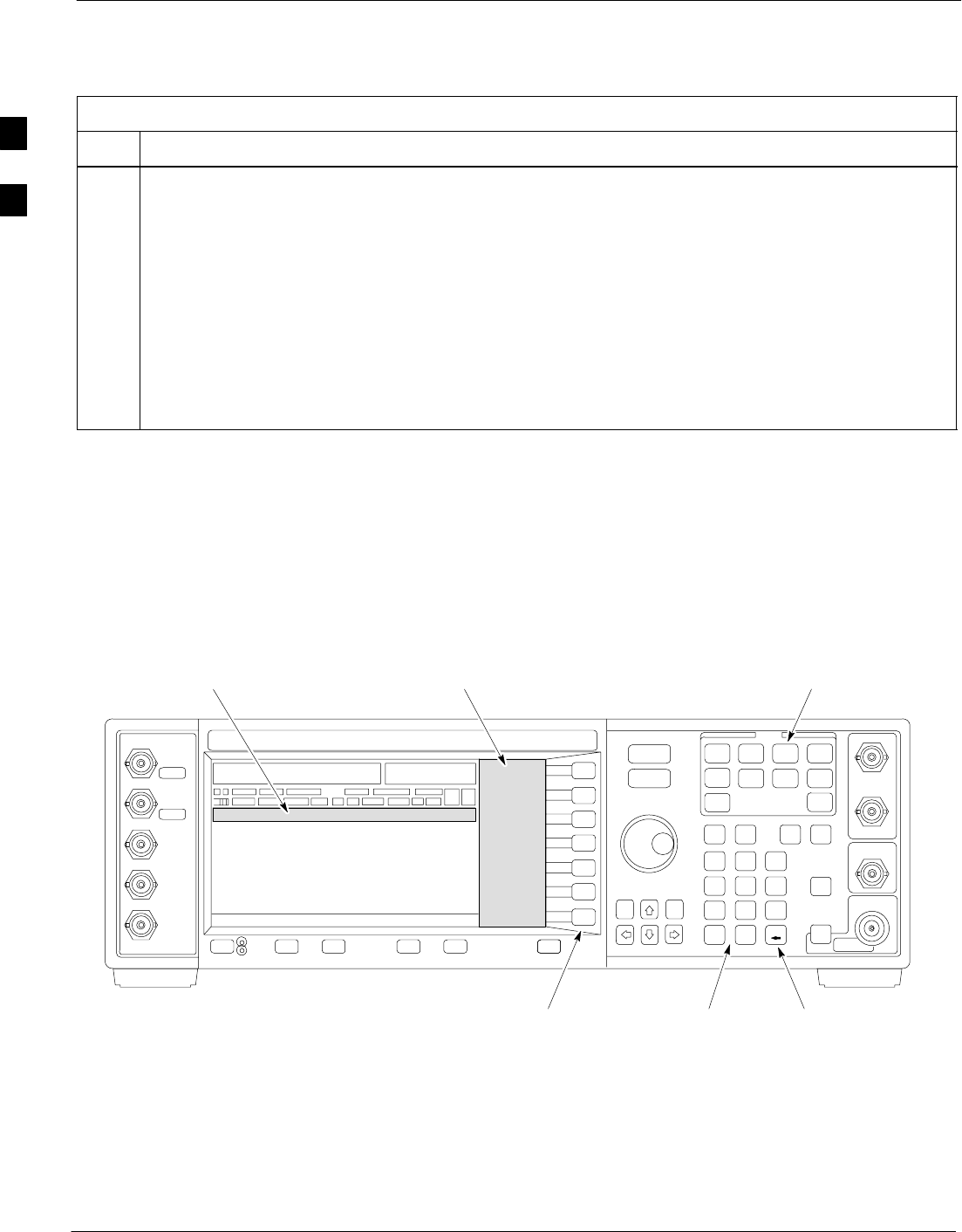
Figure B-4: Setting Agilent E4432B GPIB Address
Numeric
Keypad
Softkey
Buttons
Softkey Label
Display Area
Active Entry
Area
Backspace
Key
Utility
Key
B

Verifying and Setting GPIB Addresses – continued
MAY 2004 1X SC480 BTS Hardware Installation, Optimization/ATP, and FRU B-7
PRELIMINARY
Table B-5: Verify and Change Agilent E4432B GPIB Address
Step Action
1In the MENUS section of the instrument front panel, press the Utility key.
– The softkey labels displayed on the right side of the instrument screen will change.
2Press the GPIB/RS232 softkey button to the right of the instrument screen.
– The softkey labels will change.
– The current instrument GPIB address will be displayed below the GPIB Address softkey label.
3If the current GPIB address is not set to 1, perform the following to change it:
3a Press the GPIB Address softkey button.
– The GPIB Address label and current GPIB address will change to boldface.
– In the on–screen Active Entry Area, Address: will be displayed followed by the current GPIB
address.
3b On the front panel Numeric keypad, enter the signal generator GPIB address of 1.
– The GPIB Address label will change to Enter.
– Characters typed on the keypad will replace the current GPIB address in the Active Entry display.
NOTE
To correct an entry, press the backspace key at the lower right of the keypad to delete one character at
a time.
3c Press the Enter softkey button to set the new GPIB address.
– The new GPIB address will be displayed under the GPIB Address softkey label.
Advantest R3267 Spectrum
Analyzer GPIB Address
Refer to Figure B-5 and perform the procedure in Table B-6 to verify
and, if necessary, change the Advantest R3267 spectrum analyzer GPIB
address.
B
Verifying and Setting GPIB Addresses – continued
B-8 1X SC480 BTS Hardware Installation, Optimization/ATP, and FRU MAY 2004
PRELIMINARY
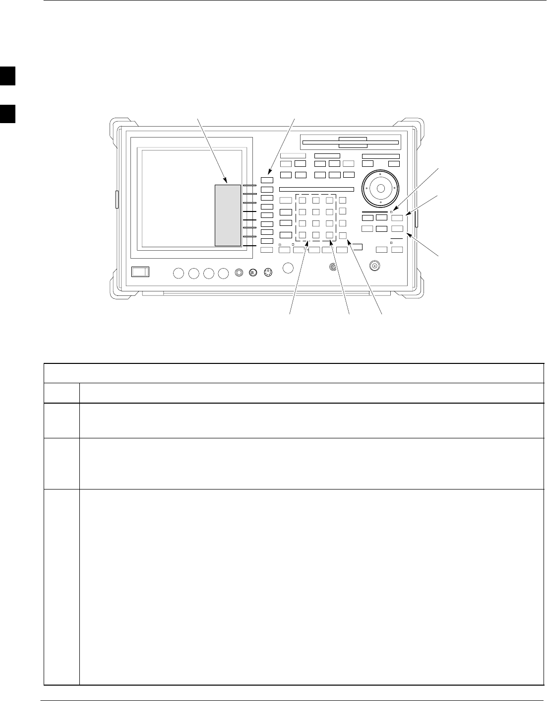
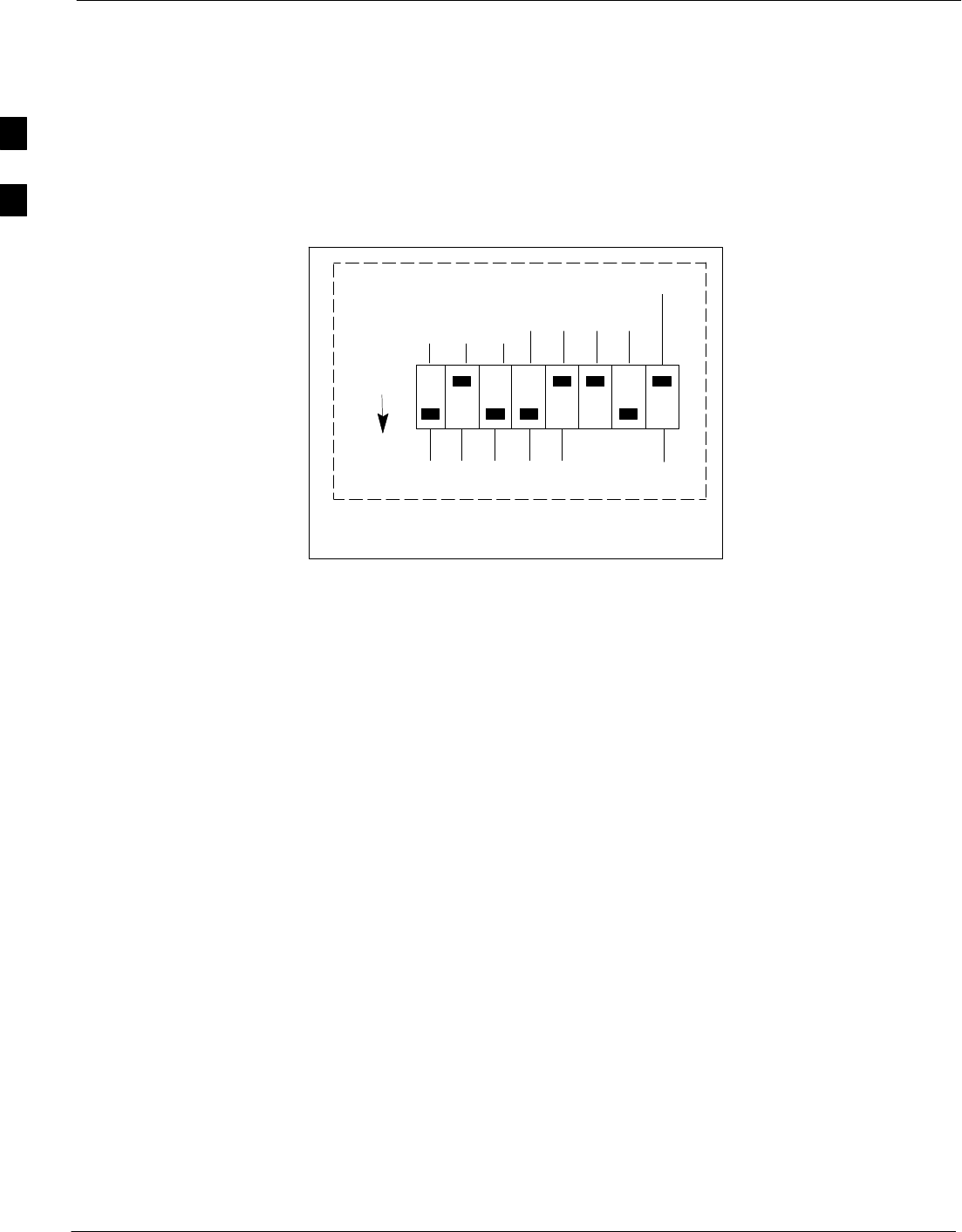
Figure B-5: Setting Advantest R3267 GPIB Address
onREMOTE
LED
LCL Key
CONFIG
Key
Softkey Lable
Display Area Softkey
Buttons
Keypad BS
Key ENTR
Key
Table B-6: Verify and Change Advantest R3267 GPIB Address
Step Action
1If the REMOTE LED is lighted, press the LCL key.
– The LED extinguishes.
2Press the CONFIG key.
–CONFIG softkey labels will appear in the softkey label display area of the instrument display.
– The current GPIB address will be displayed below the GPIB Address softkey label.
3If the current GPIB address is not set to 18, perform the following to change it:
3a Press the GPIB Address softkey. A GPIB Address entry window will open in the instrument display
showing the current GPIB address.
3b Enter 18 on the keypad in the ENTRY section of the instrument front panel.
– Characters typed on the keypad will replace the address displayed in the GPIB Address entry
window.
NOTE
To correct an entry, press the BS (backspace) key at the lower right of the keypad to delete one
character at a time.
3c Press the ENTR key to the lower right of the keypad to set the new GPIB address.
– The GPIB Address entry window closes.
– The new address is displayed in the bottom portion of the GPIB Address softkey label.
B
Verifying and Setting GPIB Addresses – continued
MAY 2004 1X SC480 BTS Hardware Installation, Optimization/ATP, and FRU B-9
PRELIMINARY
Advantest R3562 Signal
Generator GPIB Address
Set the GP–IB ADDRESS switch on the rear of the Advantest R3562
signal generator to address 1 as shown in Figure B-6.
Figure B-6: Advantest R3562 GPIB Address Switch Setting
123 4567 8
54321
GP–IP ADDRESS
1
0
GPIB Address set to “1”
Agilent 8935 Series E6380
(formerly HP 8935) Test Set
GPIB Address
Refer to Figure B-7 and follow the procedure in Table B-7 to verify and,
if necessary, change the Agilent 8935 GPIB address.
Figure B-7: Agilent 8935 Test Set
Pre-
set
Cursor Control
Shift
Inst Con-
fig
Local
FW00885
NOTE This procedure assumes that the test equipment is set up and
ready for testing.
B

Verifying and Setting GPIB Addresses – continued
B-10 1X SC480 BTS Hardware Installation, Optimization/ATP, and FRU MAY 2004
PRELIMINARY
Table B-7: Verify and/or Change Agilent 8935 (formerly HP 8935) GPIB Address
Step Action
1NOTE
The HP I/O configuration MUST be set to Talk & Listen, or no device on the GPIB will be
accessible. (Consult test equipment OEM documentation for additional information as required.)
To verify that the GPIB addresses are set correctly, press Shift and LOCAL on the Agilent 8935.
– The current HP–IB address is displayed at the top of the screen.
NOTE
HP–IB is the same as GPIB.
2If the current GPIB address is not set to 18, perform the following to change it:
2a – Press Shift and Inst Config.
2b – Turn the Cursor Control knob to move the cursor to the HP–IB Adrs field.
2c – Press the Cursor Control knob to select the field.
2d – Turn the Cursor Control knob as required to change the address to 18.
2e – Press the Cursor Control knob to set the address.
3 Press Preset to return to normal operation.
B
Verifying and Setting GPIB Addresses – continued
MAY 2004 1X SC480 BTS Hardware Installation, Optimization/ATP, and FRU B-11
PRELIMINARY
Hewlett Packard HP8921A and
HP83236A/B GPIB Address
Refer to Figure B-8 and follow the procedure in Table B-8 to verify and,
if necessary, change the HP 8921A HP 83236A GPIB addresses.
Figure B-8: HP 8921A and HP 83236A/B
Preset
Cursor Control
Shift
Local
NOTE This procedure assumes that the test equipment is set up and
ready for testing.
Table B-8: Verify and/or Change HP 8921A and HP 83236A GPIB Addresses
Step Action
1To verify that the GPIB addresses are set correctly, press Shift and LOCAL on the HP 8921A.
– The current HP–IB address is displayed at the top of the screen.
NOTE
HP–IB is the same as GPIB.
2If the current HP–IB address is not set to 18, perform the following to change it:
2a – Turn the Cursor Control knob to move the cursor to More and press the knob to select the field.
2b – Turn the Cursor Control knob to move the cursor to I/O Config and press the knob to select the
field.
2c – Turn the Cursor Control knob to move the cursor to Adrs and press the knob to select the field.
2d – Turn the Cursor Control knob to change the HP–IB address to 18 and press the knob to set the
address.
B
Verifying and Setting GPIB Addresses – continued
B-12 1X SC480 BTS Hardware Installation, Optimization/ATP, and FRU MAY 2004
PRELIMINARY
Table B-8: Verify and/or Change HP 8921A and HP 83236A GPIB Addresses
Step Action
2e – Press Shift and Preset to return to normal operation.
3To set the HP 83236A (or B) PCS Interface GPIB address=19, set the DIP switches as follows:
– A1=1, A2=1, A3=0, A4=0, A5=1, HP–IB/Ser = 1
Advantest R3465
Communications Test Set GPIB
Address
Refer to Figure B-9 and follow the procedure in Table B-9 to verify and,
if necessary, change the GPIB address for the Advantest R3465.
Figure B-9: R3465 Communications Test Set
BNC
“T”
REF UNLOCK EVEN
SEC/SYNC IN CDMA
TIME BASE IN
POWER
OFF ON
REF FW00337
LCL Shift Preset
GPIB and others
Vernier
Knob
NOTE This procedure assumes that the test equipment is set up and
ready for testing.
Table B-9: Verify and/or Change Advantest R3465 GPIB Address
Step Action
1To verify that the GPIB address is set correctly, perform the following:
1a – Press SHIFT then PRESET.
1b – Press LCL.
1c – Press the GPIB and Others CRT menu key to view the current address.
2If the current GPIB address is not set to 18, perform the following to change it:
2a – Turn the vernier knob as required to select 18.
B

Verifying and Setting GPIB Addresses – continued
MAY 2004 1X SC480 BTS Hardware Installation, Optimization/ATP, and FRU B-13
PRELIMINARY
Table B-9: Verify and/or Change Advantest R3465 GPIB Address
Step Action
2b – Press the vernier knob to set the address.
3To return to normal operation, press Shift and Preset.
Motorola CyberTest GPIB
Address
Follow the steps in Table B-10 to verify and, if necessary, change the
GPIB address on the Motorola CyberTest. Changing the GPIB address
requires the following items:
SMotorola CyberTest communications analyzer.
SComputer running Windows 3.1/Windows 95.
SMotorola CyberTAME software program “TAME”.
SParallel printer port cable (shipped with CyberTest).
NOTE This procedure assumes that the test equipment is set up and
ready for testing.
Table B-10: Verify and/or Change Motorola CyberTest GPIB Address
Step Action
1On the LMF desktop, locate the CyberTAME icon. Double click on the icon to run the CyberTAME
application.
2In the CyberTAME window taskbar, under Special, select IEEE.488.2.
3CyberTAME software will query the CyberTest Analyzer for its current GPIB address. It then will
open the IEEE 488.2 dialog box. If the current GPIB address is not 18, perform the following
procedure to change it:
3a Use the up or down increment arrows or double–click in the field and type the number to set the
address to 18.
3b Click on the OK button. The new address will be written to the CyberTest through the parallel port
and saved.
4Verify that the address has been set by repeating steps 2 and 3. The new address should now appear in
the IEEE 488.2 dialog box Address field.
B
Verifying and Setting GPIB Addresses – continued
B-14 1X SC480 BTS Hardware Installation, Optimization/ATP, and FRU MAY 2004
PRELIMINARY
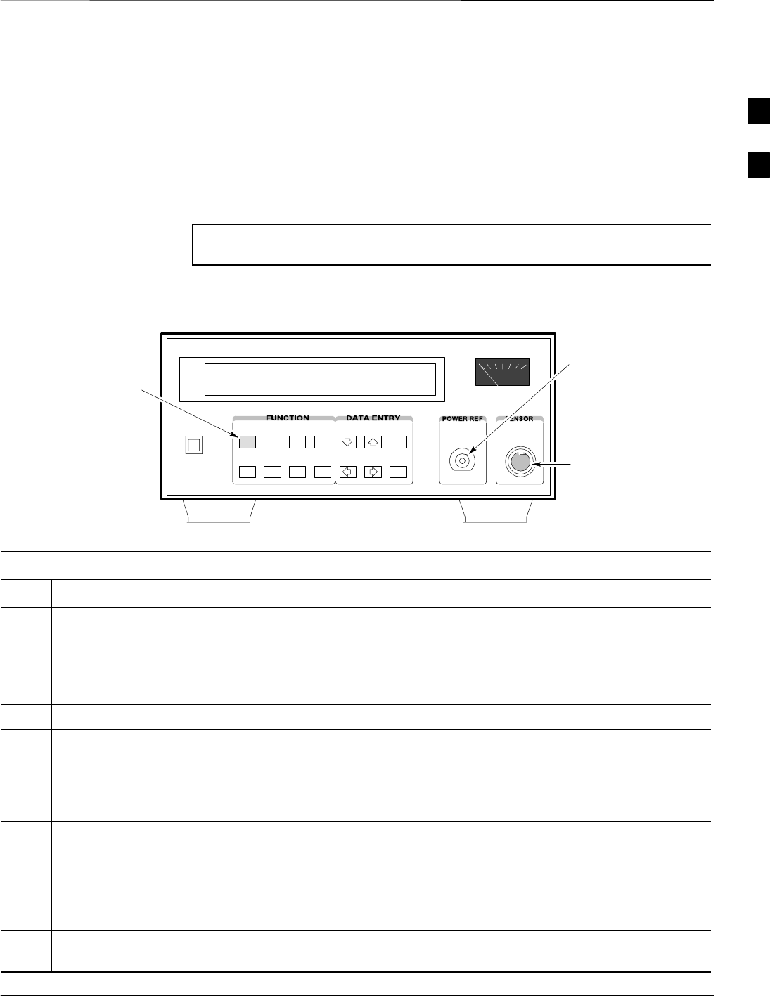
HP 437 Power Meter GPIB
Address
Refer to Figure B-10 and follow the steps in Table B-11 to verify and, if
necessary, change the HP 437 GPIB address.
Figure B-10: HP 437 Power Meter
ENTER
PRESET
SHIFT (BLUE) PUSHBUTTON –
ACCESSES FUNCTION AND
DATA ENTRY KEYS IDENTIFIED
WITH LIGHT BLUE TEXT ON
THE FRONT PANEL ABOVE
THE BUTTONS
FW00308REF
NOTE This procedure assumes that the test equipment is set up and
ready for testing.
Table B-11: Verify and/or Change HP 437 Power Meter GPIB Address
Step Action
1 Press Shift and PRESET.
2Use the y arrow key to navigate to HP–IB ADRS and press ENTER.
The HP–IB address is displayed.
NOTE
HP–IB is the same as GPIB.
3If the current GPIB address is not set to 13, perform the following to change it:
– Use the y b arrow keys to change the HP–IB ADRS to 13.
– Press ENTER to set the address.
4 Press Shift and ENTER to return to a standard configuration.
B

Verifying and Setting GPIB Addresses – continued
MAY 2004 1X SC480 BTS Hardware Installation, Optimization/ATP, and FRU B-15
PRELIMINARY
Gigatronics 8541C Power
Meter GPIB Address
Refer to Figure B-11 and follow the steps in Table B-12 to verify and, if
necessary, change the Gigatronics 8541C power meter GPIB address.
Figure B-11: Gigatronics 8541C Power Meter Detail
NOTE This procedure assumes that the test equipment is set up and
ready for testing.
Table B-12: Verify and/or Change Gigatronics 8541C Power Meter GPIB Address
Step Action
1! CAUTION
Do not connect/disconnect the power meter sensor cable with AC power applied to the meter.
Disconnection could result in destruction of the sensing element or miscalibration.
Press MENU.
2Use the b arrow key to select CONFIG MENU and press ENTER.
3Use the b arrow key to select GPIB and press ENTER.
The current Mode and GPIB Address are displayed.
4If the Mode is not set to 8541C, perform the following to change it:
Use the a ’ arrow keys as required to select MODE.
Use the by arrow keys as required to set MODE to 8541C.
5If the GPIB address is not set to 13, perform the following to change it:
Use the ’ arrow key to select ADDRESS.
Use the by arrow keys as required to set the GPIB address to 13.
6 Press ENTER to return to normal operation.
B
Verifying and Setting GPIB Addresses – continued
B-16 1X SC480 BTS Hardware Installation, Optimization/ATP, and FRU MAY 2004
PRELIMINARY
RS232 GPIB Interface Adapter
Be sure that the RS–232 GPIB interface adapter DIP switches are set as
shown in Figure B-12.
Figure B-12: RS232 GPIB Interface Adapter
RS232–GPIB
INTERFACE BOX
S MODE
DATA FORMAT
BAUD RATE
GPIB ADRS
ON
DIP SWITCH SETTINGS
G MODE
B

Test Equipment Connection, Testing, and Control
MAY 2004 1X SC480 BTS Hardware Installation, Optimization/ATP, and FRU B-17
PRELIMINARY
Inter–unit Connection, Testing,
and Control Settings
The following illustrations, tables, and procedures provide the
information necessary to prepare various items of CDMA test equipment
supported by the WinLMF for BTS calibration and/or acceptance testing.
HP 8921A with PCS Interface
Test Equipment Connections
The following diagram depicts the rear panels of the HP 8921A test
equipment as configured to perform automatic tests. All test equipment
is controlled by the WinLMF via an IEEE–488/GPIB bus. The WinLMF
expects each piece of test equipment to have a factory-set GPIB address
(refer to Table B-8 and Figure B-8). If there is a communications
problem between the WinLMF and any piece of test equipment, verify
that the GPIB addresses have been set correctly and that the GPIB cables
are firmly connected to the test equipment.
Table B-13 shows the connections when not using an external 10 MHz
Rubidium reference.
Table B-13: HP 8921A/600 Communications Test Set Rear Panel Connections Without Rubidium Reference
From Test Set: To Interface:
Connector Type
8921A 83203B CDMA 83236A PCS
Connector Type
CW RF OUT CW RF IN SMC–female – SMC–female
114.3 MHZ IF OUT 114.3 MHZ IF IN SMC–female – SMC–female
IQ RF IN IQ RF OUT SMC–female – SMC–female
DET OUT AUX DSP IN SMC–female – SMC–female
CONTROL I/O CONTROL I/O 45–pin custom BUS
10 MHZ OUT SYNTH REF IN BNC–male – BNC–male
HPIB INTERFACE HPIB INTERFACE HPIB cable
10 MHZ OUT REF IN BNC–male – BNC–male
B
Test Equipment Connection, Testing, and Control – continued
B-18 1X SC480 BTS Hardware Installation, Optimization/ATP, and FRU MAY 2004
PRELIMINARY
REAR PANEL
COMMUNICATIONS TEST SET
REF IN
HP 83203B CDMA
CELLULAR ADAPTER
HP 8921A CELL
SITE TEST SET
HP 83236A PCS
INTERFACE
HP–IB
TO GPIB
INTERFACE
BOX
TO POWER
METER GPIB
CONNECTOR
FW00368
Figure B-13: HP 8921A/600 Cable Connections for 10 MHz Signal and GPIB
without Rubidium Reference
B

Test Equipment Connection, Testing, and Control – continued
MAY 2004 1X SC480 BTS Hardware Installation, Optimization/ATP, and FRU B-19
PRELIMINARY
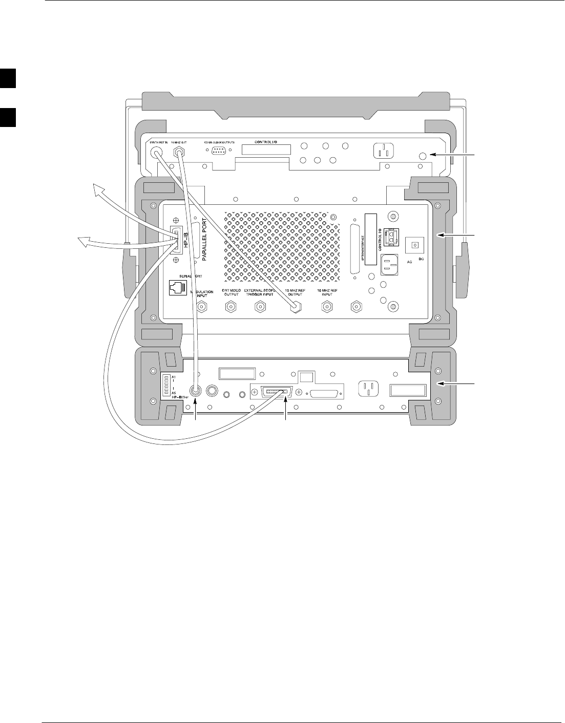
Figure B-14 shows the connections when using an external 10 MHz
Rubidium reference.
Table B-14: HP 8921A/600 Communications Test Set Rear Panel Connections With Rubidium Reference
From Test Set: To Interface:
Connector Type
8921A 83203B CDMA 83236A PCS
Connector Type
CW RF OUT CW RF IN SMC–female – SMC–female
114.3 MHZ IF OUT 114.3 MHZ IF IN SMC–female – SMC–female
IQ RF IN IQ RF OUT SMC–female – SMC–female
DET OUT AUX DSP IN SMC–female – SMC–female
CONTROL I/O CONTROL I/O 45–pin custom BUS
10 MHZ OUT REF IN BNC–male – BNC–male
HPIB INTERFACE HPIB INTERFACE HPIB cable
10 MHZ INPUT 10 MHZ OUT BNC–male – BNC–male
B
Test Equipment Connection, Testing, and Control – continued
B-20 1X SC480 BTS Hardware Installation, Optimization/ATP, and FRU MAY 2004
PRELIMINARY
REF IN
REAR PANEL
COMMUNICATIONS TEST SET
TO POWER
METER GPIB
CONNECTOR
TO GPIB
INTERFACE
BOX
10 MHZ WITH
RUBIDIUM STANDARD
HP 83203B CDMA
CELLULAR ADAPTER
HP 8921A CELL
SITE TEST SET
HP 83236A PCS
INTERFACE
HP–IB
FW00369
Figure B-14: HP 8921A Cable Connections for 10 MHz Signal and GPIB with Rubidium Reference
B

Test Equipment Connection, Testing, and Control – continued
MAY 2004 1X SC480 BTS Hardware Installation, Optimization/ATP, and FRU B-21
PRELIMINARY
HP 8921A with PCS Interface
System Connectivity Test
Follow the steps outlined in Table B-15 to verify that the connections
between the PCS Interface and the HP 8921A are correct and cables are
intact. The software also performs basic functionality checks of each
instrument.
Disconnect other GPIB devices, especially system
controllers, from the system before running the
connectivity software.
NOTE
Table B-15: System Connectivity
Step Action
NOTE
– Perform this procedure after test equipment has been allowed to warm–up and stabilize for a
minimum of 60 minutes.
1Insert HP 83236A Manual Control/System card into memory card slot.
2Press the [PRESET] pushbutton.
3Press the Screen Control [TESTS] pushbutton to display the “Tests” Main Menu screen.
4Position the cursor at Select Procedure Location and select it by pressing the cursor control knob. In
the Choices selection box, select Card.
5Position the cursor at Select Procedure Filename and select it by pressing the cursor control knob. In
the Choices selection box, select SYS_CONN.
6Position the cursor at RUN TEST and select it. The software will provide operator prompts through
completion of the connectivity setup.
7Do the following when the test is complete,
Sposition cursor on STOP TEST and select it
SOR press the [K5] pushbutton.
8To return to the main menu, press the [K5] pushbutton.
9Press the [PRESET] pushbutton.
Pretest Setup for HP 8921A
Before the HP 8921A CDMA analyzer is used for WinLMF–controlled
testing it must be set up correctly for automatic testing. Perform the
procedure in Table B-16.
B

Test Equipment Connection, Testing, and Control – continued
B-22 1X SC480 BTS Hardware Installation, Optimization/ATP, and FRU MAY 2004
PRELIMINARY
Table B-16: Pretest Setup for HP 8921A
Step Action
1Unplug the memory card if it is plugged in.
2Press the CURSOR CONTROL knob.
3Position the cursor at IO CONFIG (under To Screen and More) and select it.
4Select Mode and set for Talk&Lstn.
Pretest Setup for Agilent 8935
Before the Agilent 8935 analyzer is used for WinLMF controlled testing
it must be set up correctly for automatic testing. Perform the procedure
in Table B-17.
Table B-17: Pretest Setup for Agilent 8935
Step Action
1Unplug the memory card if it is plugged in.
2Press the Shift button and then press the I/O Config button.
3Press the Push to Select knob.
4Position the cursor at IO CONFIG and select it.
5 Select Mode and set for Talk&Lstn.
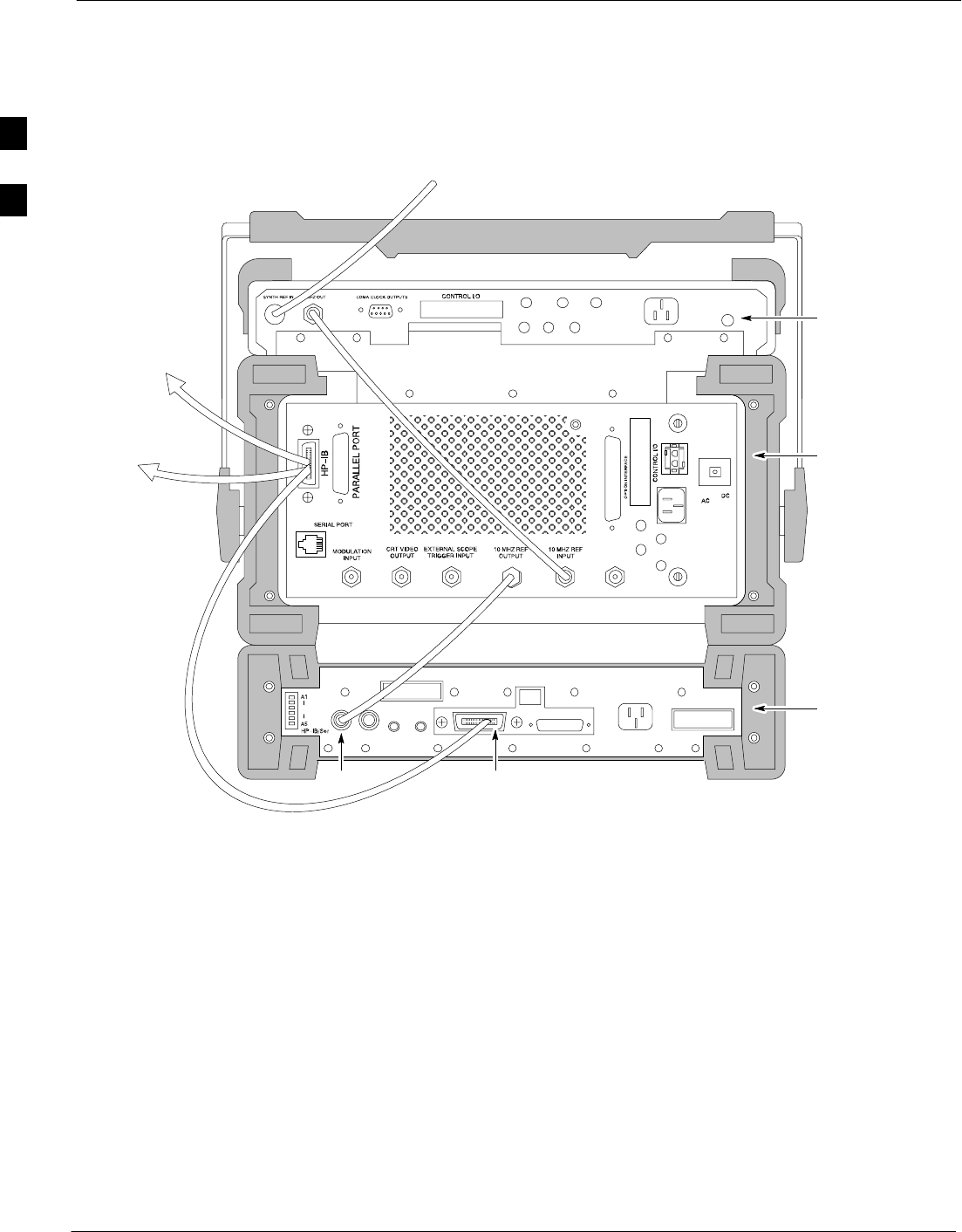
Advantest R3465 Connection
The following diagram depicts the rear panels of the Advantest R3465
test equipment as configured to perform automatic tests. All test
equipment is controlled by the WinLMF via an IEEE–488/GPIB bus.
The WinLMF expects each piece of test equipment to have a factory-set
GPIB address (refer to Table B-9 and Figure B-9). If there is a
communications problem between the WinLMF and any piece of test
equipment, verify that the GPIB addresses have been set correctly and
that the GPIB cables are firmly connected to the test equipment.
Figure B-15 shows the connections when not using an external 10 MHz
Rubidium reference.
B
Test Equipment Connection, Testing, and Control – continued
MAY 2004 1X SC480 BTS Hardware Installation, Optimization/ATP, and FRU B-23
PRELIMINARY
ADVANTEST R3465
REAR PANEL
GPIB
CONNECTOR
SERIAL I/O
LOCAL IN
SERIAL I/O
SYN REF IN 10 MHZ OUT
PARALLEL
EXT TRIGGER
10 MHZ REF
GATE IN
GPIB
CDMA CLOCK OUT
AC POWER
AC POWER
R3561L
REAR PANEL
R3465
REAR PANEL
TO T–CONNECTOR
ON FRONT PANEL
(EVEN/SEC/SYNC IN)
XYZ
IF OUT
421 MHZ
TO POWER METER
GPIB CONNECTOR
TO GPIB
INTERFACE BOX
FW00370
Figure B-15: Cable Connections for Test Set without 10 MHz Rubidium Reference
B
Test Equipment Connection, Testing, and Control – continued
B-24 1X SC480 BTS Hardware Installation, Optimization/ATP, and FRU MAY 2004
PRELIMINARY
Figure B-16 shows the connections when using an external 10 MHz
Rubidium reference.
SERIAL I/O
GPIB
CONNECTOR ADVANTEST R3465
REAR PANEL
FROM 10 MHZ
RUBIDIUM REFERENCE
LOCAL IN
SERIAL I/O
IF OUT
SYN REF IN 10 MHZ OUT
PARALLEL
EXT TRIGGER
10 MHZ REF
GATE IN
GPIB
CDMA CLOCK OUT
AC POWER
AC POWER
R3465/3463
REAR PANEL
R3561L
REAR PANEL
TO T–CONNECTOR
ON FRONT PANEL
(EVEN SEC/SYNC IN)
XYZ
421 MHZ
TO POWER METER
GPIB CONNECTOR
TO GPIB
INTERFACE BOX
FW00371
Figure B-16: Cable Connections for Test Set with 10 MHz Rubidium Reference
R3465 GPIB Clock Set–up
Table B-18 describes the steps to set the clock for the Advantest R3465
equipment.
Table B-18: Advantest R3465 Clock Setup
Step Action
1Observe the current date and time displayed in upper right of the CRT display.
2If the date and time are incorrect, perform the following to change them:
2a – Push the Date/Time CRT menu key.
2b – Rotate the vernier knob to select and set.
2c – Push the vernier knob to enter.
2d – Push the SHIFT then PRESET pushbutton (just below the CRT display).
B

Test Equipment Connection, Testing, and Control – continued
MAY 2004 1X SC480 BTS Hardware Installation, Optimization/ATP, and FRU B-25
PRELIMINARY
Pretest Setup for Advantest
R3465
Before the Advantest R3465 analyzer is used for WinLMF–controlled
testing it must be set up correctly for automatic testing. Perform the
procedure in Table B-19.
Table B-19: Pretest Setup for Advantest R3465
Step Action
1Press the SHIFT button so the LED next to it is illuminated.
2Press the RESET button.
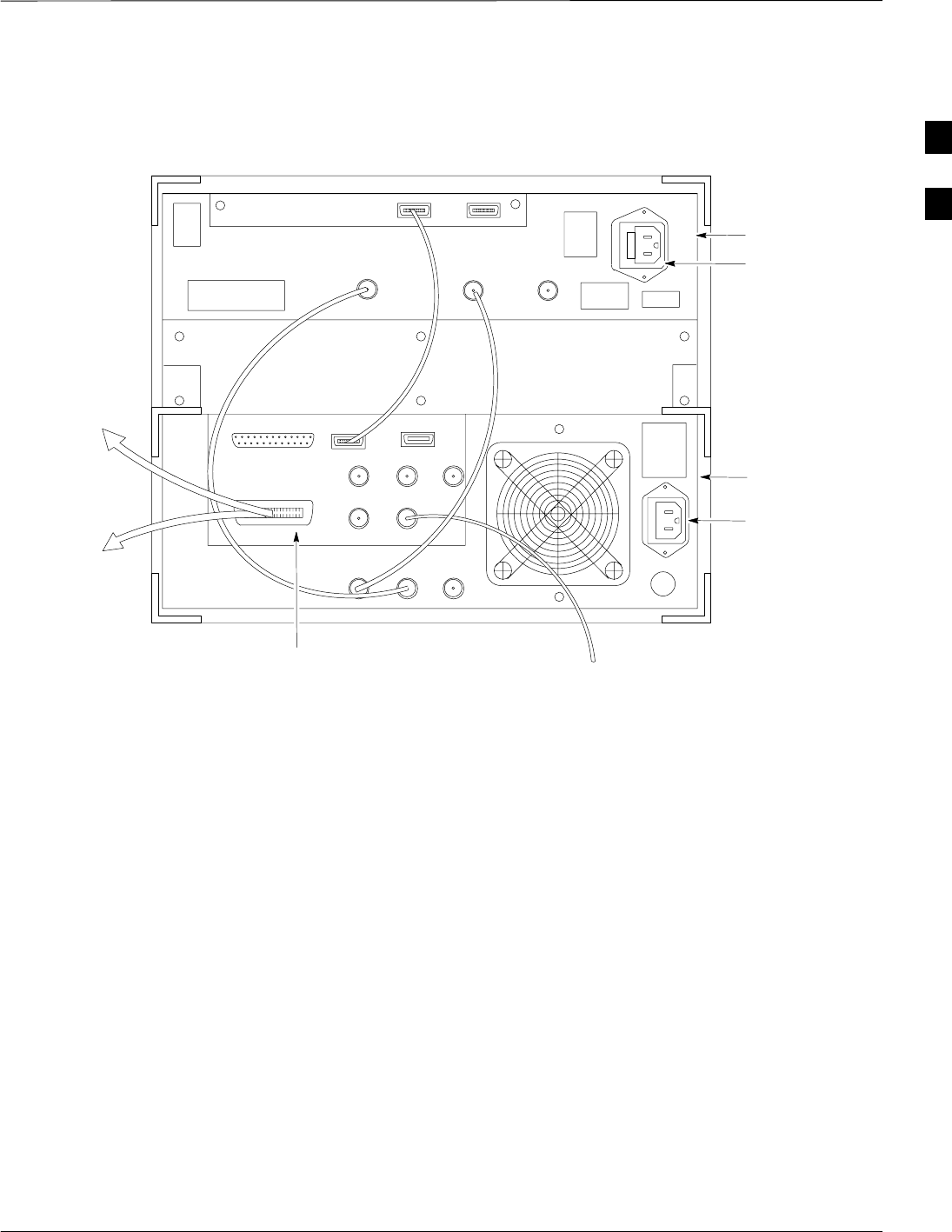
Agilent 8932/E4432B Test
Equipment Interconnection
To perform FER testing on a 1X BTS with the Agilent 8935, a
1X–capable signal generator, such as the Agilent E4432B, must be used
in conjunction with the CDMA base station test set. For proper
operation, the test equipment items must be interconnected as follows:
10 MHz reference signal – Connect a BNC (M)–BNC (M) cable from
the 8935 10 MHz REF OUT connector to the E4432B 10MHz IN
connector as shown in Figure B-17
Even second pulse reference – Refer to Figure B-17, and connect a
BNC “T” connector to the 8935 EVEN SEC SYNC IN connector.
Connect a BNC (M)–BNC (M) cable from one side of the BNC “T” to
the E4432B PATTERN TRIG IN connector. Connect the other side of
the BNC “T” to the CSA Card SYNC MONITOR connector using a
BNC (M)–BNC (M) cable.
B
Test Equipment Connection, Testing, and Control – continued
B-26 1X SC480 BTS Hardware Installation, Optimization/ATP, and FRU MAY 2004
PRELIMINARY
E4432B
10 MHz IN
TO GPIB
E4432B
PATTERN TRIG IN
TO CSA CARD
SYNC MONITOR
(EVEN SEC TICK)
8935
10 MHz
REF OUT
8935
EVEN SECOND
SYNC IN
WITH BNC “T” TDME0011–1
Figure B-17: Agilent 8935/E4432B 10MHz Reference and Even Second Tick Connections
Agilent E4406A/E4432B Test
Equipment Interconnection
To provide proper operation during testing when both units are required,
the 10 MHz reference signal from the E4406A transmitter test set must
be provided to the E4432B signal generator. Connect a BNC (M)–BNC
(M) cable from the E4406A 10 MHz OUT (SWITCHED) connector to
the E4432B 10MHz IN connector as shown in Figure B-18.
E4406A
10 MHz OUT
(SWITCHED)
E4432B
10 MHz IN
TO GPIB BOX
TDME0009–1
Figure B-18: Agilent 10 MHz Reference Connections
B
Test Equipment Connection, Testing, and Control – continued
MAY 2004 1X SC480 BTS Hardware Installation, Optimization/ATP, and FRU B-27
PRELIMINARY
Advantest R3267/R3562 Test
Equipment Interconnection
To provide proper operation during testing when both units are required,
the R3257 spectrum analyzer must be interconnected with the R3562
signal generator as follows:
10 MHz reference signal – Connect a BNC (M)–BNC (M) cable
between the R3562 SYNTHE REF IN connector and the R3267 10
MHz OUT connector as shown in Figure B-19.
Serial I/O – Using the Advantest cable provided, connect the R3267
SERIAL I/O connector to the R3562 SERIAL I/O connector as shown
in Figure B-19.
TDME0010–1
R3562
SYNTHE REF IN TO GPIB
BOX R3562
SERIAL I/O
TO GPIB BOX
R3267
10 MHZ OUT R3267
SERIAL I/O
Figure B-19: Advantest 10 MHz Reference and Serial I/O Connections
B
Equipment Calibration
B-28 1X SC480 BTS Hardware Installation, Optimization/ATP, and FRU MAY 2004
PRELIMINARY
Calibration Without the LMF
Several test equipment items used in the optimization process require
pre–calibration actions or calibration verification which are not
supported by the LMF. Procedures to perform these activities for the
applicable test equipment items are covered in this section.
Agilent E4406A Transmitter
Tester Self–alignment
(Calibration)
System
Key
Softkey
Buttons
Softkey Label
Display Area
Figure B-20: Performing Agilent E4406A
Self–alignment (Calibration)
Refer to Figure B-20 and follow the procedure in Table B-20 to perform
the Agilent E4406A self–alignment (calibration).
Table B-20: Perform Agilent E4406A Self–alignment (Calibration)
Step Action
1In the SYSTEM section of the instrument front panel, press the System key.
– The softkey labels displayed on the right side of the instrument screen will change.
2Press the Alignments softkey button to the right of the instrument screen.
– The softkey labels will change.
3Press the Align All Now softkey button.
– All other instrument functions will be suspended during the alignment.
– The display will change to show progress and results of the alignments performed.
– The alignment will take less than one minute.
B
Equipment Calibration – continued
MAY 2004 1X SC480 BTS Hardware Installation, Optimization/ATP, and FRU B-29
PRELIMINARY
Calibrating HP 437 Power
Meter
Precise transmit output power calibration measurements are made using
a bolometer–type broadband power meter with a sensitive power sensor.
Follow the steps outlined in Table B-21 to enter information unique to
the power sensor before calibrating the test setup. Refer to Figure B-21
as required.
NOTE This procedure must be done before the automated calibration to
enter power sensor specific calibration values.
Figure B-21: Power Meter Detail
CONNECT POWER
SENSOR WITH POWER
METER TURNED OFF
CONNECT POWER SENSOR
TO POWER REFERENCE
WHEN CALIBRATING UNIT.
POWER REFERENCE IS
ENABLED USING THE SHIFT ’
KEYS
SHIFT (BLUE) PUSHBUTTON –
ACCESSES FUNCTION AND
DATA ENTRY KEYS IDENTIFIED
WITH LIGHT BLUE TEXT ON
THE FRONT PANEL ABOVE
THE BUTTONS
FW00308
Table B-21: HP 437 Power Meter Calibration Procedure
Step Action
1! CAUTION
Do not connect/disconnect the power meter sensor cable with AC power applied to the meter.
Disconnection could result in destruction of the sensing element or mis–calibration.
Make sure the power meter AC LINE pushbutton is OFF.
2Connect the power sensor cable to the SENSOR input.
3Set the AC LINE pushbutton to ON.
NOTE
The calibration should be performed only after the power meter and sensor have been allowed to
warm–up and stabilize for a minimum of 60 minutes.
4Perform the following to set or verify the correct power sensor model:
4a – Press [SHIFT] then [a] to select SENSOR.
4b – Identify the power sensor model number from the sensor label.
4c – Use the [y] or [b] button to select the appropriate model; then press [ENTER].
5Refer to the illustration for step 8, and perform the following to ensure the power reference output is
OFF:
. . . continued on next page
B
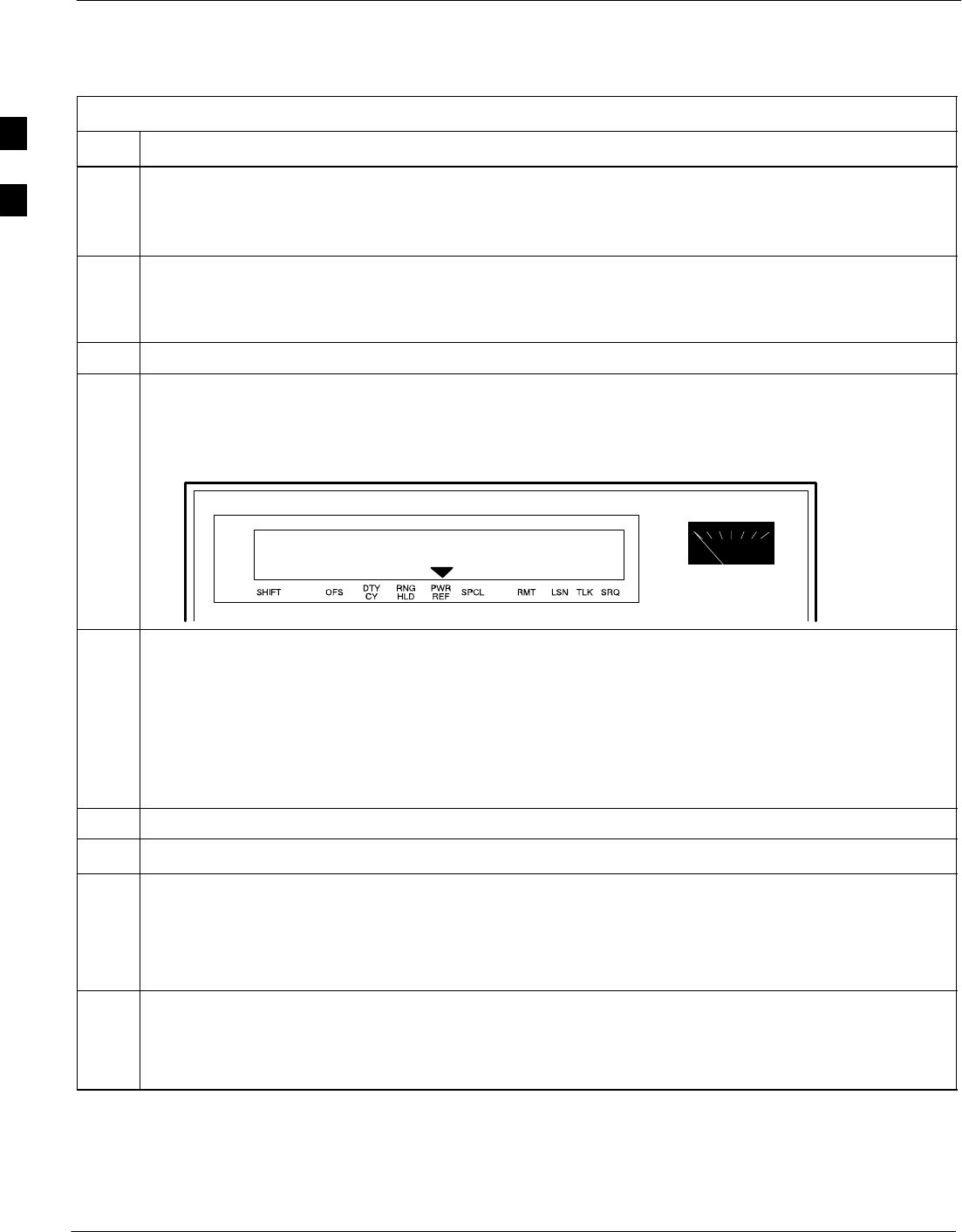
Equipment Calibration – continued
B-30 1X SC480 BTS Hardware Installation, Optimization/ATP, and FRU MAY 2004
PRELIMINARY
Table B-21: HP 437 Power Meter Calibration Procedure
Step Action
5a – Observe the instrument display and determine if the triangular indicator over PWR REF is
displayed.
5b – If the triangular indicator is displayed, press [SHIFT] then [’] to turn it off.
6 Press [ZERO].
– Display will show “Zeroing ******.”
– Wait for process to complete.
7Connect the power sensor to the POWER REF output.
8Turn on the PWR REF by performing the following:
8a – Press [SHIFT] then [’].
8b – Verify that the triangular indicator (below) appears in the display above PWR REF.
9Perform the following to set the REF CF%:
9a – Press ([SHIFT] then [ZERO]) for CAL.
9b – Enter the sensor’s REF CF% from the sensor’s decal using the arrow keys and press [ENTER].
(The power meter will display ”CAL *****” for a few seconds.)
NOTE
If the REF CAL FACTOR (REF CF) is not shown on the power sensor, assume it to be 100%.
10 Perform the following to set the CAL FAC %:
10a – Press [SHIFT] then [FREQ] for CAL FAC.
10b – On the sensor’s decal, locate an approximate calibration percentage factor (CF%) at 2 GHz.
10c – Enter the sensor’s calibration % (CF%) using the arrow keys and press [ENTER].
–– When complete, the power meter will typically display 0.05 dBm. (Any reading between
0.00 and 0.10 is normal.)
11 To turn off the PWR REF, perform the following:
11a – Press [SHIFT] then [’].
11b – Disconnect the power sensor from the POWER REF output.
B
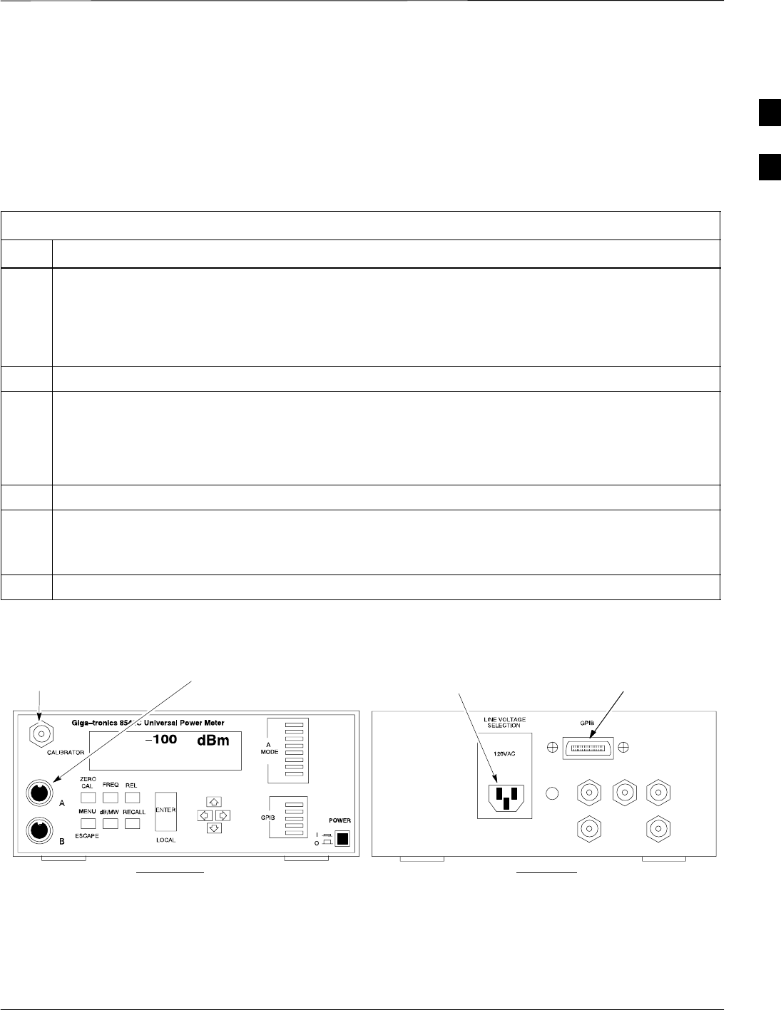
Equipment Calibration – continued
MAY 2004 1X SC480 BTS Hardware Installation, Optimization/ATP, and FRU B-31
PRELIMINARY
Calibrating Gigatronics 8541C
Power Meter
Precise transmit output power calibration measurements are made using
a bolometer–type broadband power meter with a sensitive power sensor.
Follow the steps in Table B-22 to enter information unique to the power
sensor.
Table B-22: Calibrate Gigatronics 8541C Power Meter
Step Action
1! CAUTION
Do not connect/disconnect the power meter sensor cable with AC power applied to the meter.
Disconnection could result in destruction of the sensing element or miscalibration.
Make sure the power meter POWER pushbutton is OFF.
2Connect the power sensor cable to the SENSOR input.
3Set the POWER pushbutton to ON.
NOTE
Allow the power meter and sensor to warm up and stabilize for a minimum of 60 minutes before
performing the calibration procedure.
4Connect the power sensor to the CALIBRATOR output connector.
5 Press ZERO.
– Wait for the process to complete. Sensor factory calibration data is read to power meter during this
process.
6When the zeroing process is complete, disconnect the power sensor from the CALIBRATOR output.
Figure B-22: Gigatronics 8541C Power Meter Detail
CONNECT POWER SENSOR
WITH POWER METER
TURNED OFF
CONNECT POWER SENSOR TO
CALIBRATOR POWER REFERENCE
WHEN CALIBRATING/ZEROING UNIT
FRONT View REAR View
GPIB CONNECTIONAC POWER
FW00564
B

Manual Cable Calibration
B-32 1X SC480 BTS Hardware Installation, Optimization/ATP, and FRU MAY 2004
PRELIMINARY
Calibrating Test Cable Setup
Using HP PCS Interface
(HP83236)
Table B-23 covers the procedure to calibrate the test equipment using the
HP8921 Cellular Communications Analyzer equipped with the HP83236
PCS Interface.
NOTE This calibration method must be executed with great care. Some
losses are measured close to the minimum limit of the power
meter sensor (–30 dBm).
Prerequisites
Ensure the following prerequisites have been met before proceeding:
STest equipment to be calibrated has been connected correctly for cable
calibration.
STest equipment has been selected and calibrated.
Table B-23: Calibrating Test Cable Setup (using the HP PCS Interface)
Step Action
NOTE
Verify that GPIB controller is turned off.
1Insert HP83236 Manual Control System card into memory card slot.
2Press the Preset pushbutton.
3 Under Screen Controls, press the TESTS pushbutton to display the TESTS (Main Menu) screen.
4Position the cursor at Select Procedure Location and select it. In the Choices selection box, select
CARD.
5Position the cursor at Select Procedure Filename and select it. In the Choices selection box, select
MANUAL.
6Position the cursor at RUN TEST and select it. HP must be in Control Mode Select YES.
7If using HP83236A:
Set channel number=<chan#>:
– Position cursor at Channel
Number and select it.
– Enter the chan# using the numeric
keypad; press [Enter] and the
screen will go blank.
– When the screen reappears, the
chan# will be displayed on the
channel number line.
If using HP83236B:
Set channel frequency:
– Position cursor at Frequency Band and press Enter.
– Select User Defined Frequency.
– Go Back to Previous Menu.
– Position the cursor to 83236 generator frequency and
enter actual RX frequency.
– Position the cursor to 83236 analyzer frequency and
enter actual TX frequency.
8Set RF Generator level:
– Position the cursor at RF Generator Level and select it.
– Enter –10 using the numeric keypad; press [Enter] and the screen will go blank.
– When the screen reappears, the value –10 dBm will be displayed on the RF Generator Level line.
. . . continued on next page
B

Manual Cable Calibration – continued
MAY 2004 1X SC480 BTS Hardware Installation, Optimization/ATP, and FRU B-33
PRELIMINARY
Table B-23: Calibrating Test Cable Setup (using the HP PCS Interface)
Step Action
9Set the user fixed Attenuation Setting to 0 dBm:
– Position cursor at Analyzer Attenuation and select it
– Position cursor at User Fixed Atten Settings and select it.
– Enter 0 (zero) using the numeric keypad and press [Enter].
10 Select Back to Previous Menu.
11 Record the HP83236 Generator Frequency Level:
Record the HP83236B Generator Frequency Level:
– Position cursor at Show Frequency and Level Details and select it.
– Under HP83236 Frequencies and Levels, record the Generator Level.
– Under HP83236B Frequencies and Levels, record the Generator Frequency Level (1850 – 1910
MHz).
– Position cursor at Prev Menu and select it.
12 Click on Pause for Manual Measurement.
13 Connect the power sensor directly to the RF OUT ONLY port of the PCS Interface.
14 On the HP8921A, under To Screen, select CDMA GEN.
15 Move the cursor to the Amplitude field and click on the Amplitude value.
16 Increase the Amplitude value until the power meter reads 0 dBm ±0.2 dB.
NOTE
The Amplitude value can be increased coarsely until 0 dBM is reached; then fine tune the amplitude
by adjusting the Increment Set to 0.1 dBm and targeting in on 0 dBm.
17 Disconnect the power sensor from the RF OUT ONLY port of the PCS Interface.
NOTE
The Power Meter sensor’s lower limit is –30 dBm. Thus, only components having losses ≤30 dB
should be measured using this method. For further accuracy, always re-zero the power meter
before connecting the power sensor to the component being calibrated. After connecting the
power sensor to the component, record the calibrated loss immediately.
18 Disconnect all components in the test setup and calibrate each one separately by connecting each
component, one-at-a-time, between the RF OUT ONLY PORT and the power sensor. Record the
calibrated loss value displayed on the power meter.
SExample: (A) Test Cable(s) = –1.4 dB
(B) 20 dB Attenuator = –20.1 dB
(B) Directional Coupler = –29.8 dB
19 After all components are calibrated, reassemble all components together and calculate the total test
setup loss by adding up all the individual losses:
SExample: Total test setup loss = –1.4 –29.8 –20.1 = –51.3 dB.
This calculated value will be used in the next series of tests.
20 Under Screen Controls press the TESTS button to display the TESTS (Main Menu) screen.
. . . continued on next page
B

Manual Cable Calibration – continued
B-34 1X SC480 BTS Hardware Installation, Optimization/ATP, and FRU MAY 2004
PRELIMINARY
Table B-23: Calibrating Test Cable Setup (using the HP PCS Interface)
Step Action
21 Select Continue (K2).
22 Select RF Generator Level and set to –119 dBm.
23 Click on Pause for Manual Measurement.
24 Verify the HP8921A Communication Analyzer/83203A CDMA interface setup is as follows (fields
not indicated remain at default):
SVerify the GPIB (HP–IB) address:
– under To Screen, select More
– select IO CONFIG
– Set HP–IB Adrs to 18
– set Mode to Talk&Lstn
SVerify the HP8921A is displaying frequency (instead of RF channel)
– Press the blue [SHIFT] button, then press the Screen Control [DUPLEX] button; this switches to
the CONFIG (CONFIGURE) screen.
– Use the cursor control to set RF Display to Freq
25 Refer toChapter 3 for assistance in setting the cable loss values into the LMF.
B
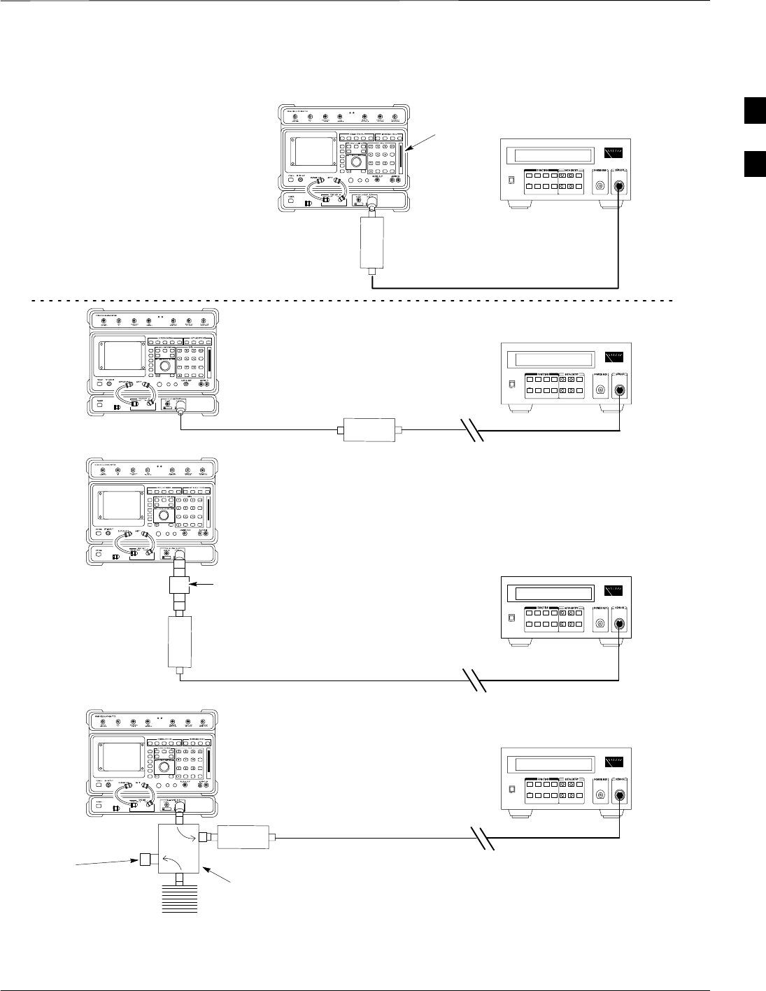
Manual Cable Calibration – continued
MAY 2004 1X SC480 BTS Hardware Installation, Optimization/ATP, and FRU B-35
PRELIMINARY
Figure B-23: Cable Calibration Using HP8921 with PCS Interface
(A)
(C)
(A)
POWER
SENSOR
(C)
30 dB
DIRECTIONAL
COUPLER
150 W
NON–RADIATING
RF LOAD
POWER
SENSOR
(B)
POWER
SENSOR
(B)
MEMORY
CARD
SLOT
20 dB / 20 WATT
ATTENUATOR
FW00292
50 Ω
TERMINATION
POWER
SENSOR
B

Manual Cable Calibration – continued
B-36 1X SC480 BTS Hardware Installation, Optimization/ATP, and FRU MAY 2004
PRELIMINARY
Calibrating Test Cable Setup
Using Advantest R3465
NOTE Be sure the GPIB Interface is OFF for this procedure.
Advantest R3465 Manual Test setup and calibration must be performed
at both the TX and RX frequencies.
Table B-24: Procedure for Calibrating Test Cable Setup Using Advantest R3465
Step Action
* IMPORTANT
– This procedure can only be performed after test equipment has been allowed to warm–up and
stabilize for a minimum of 60 minutes.
1Press the SHIFT and the PRESET keys located below the display
2Press the ADVANCE key in the MEASUREMENT area of the control panel.
3Select the CDMA Sig CRT menu key
4Select the Setup CRT menu key
5Using the vernier knob and the cursor keys set the following parameters
NOTE
Fields not listed remain at default
Generator Mode: SIGNAL
Link: FORWARD
Level Unit: dBm
CalCorrection: ON
Level Offset: OFF
6Select the return CRT menu key
7 Press FREQ key in the ENTRY area
8Set the frequency to the desired value using the keypad entry keys
9Verify that the Mod CRT menu key is highlighting OFF; if not, press the Mod key to toggle it OFF.
10 Verify that the Output CRT menu key is highlighting OFF; if not, press the Output key to toggle it
OFF.
11 Press the LEVEL key in the ENTRY area.
12 Set the LEVEL to 0 dBm using the key pad entry keys.
13 Zero power meter. Next connect the power sensor directly to the “RF OUT” port on the R3561L
CDMA Test Source Unit.
14 Press the Output CRT menu key to toggle Output to ON.
15 Record the power meter reading ________________________
. . . continued on next page
B

Manual Cable Calibration – continued
MAY 2004 1X SC480 BTS Hardware Installation, Optimization/ATP, and FRU B-37
PRELIMINARY
Table B-24: Procedure for Calibrating Test Cable Setup Using Advantest R3465
Step Action
16 Disconnect the power meter sensor from the R3561L RF OUT jack.
* IMPORTANT
The Power Meter sensor’s lower limit is –30 dBm. Thus, only components having losses < 30 dB
should be measured using this method. For best accuracy, always re–zero the power meter before
connecting the power sensor to the component being calibrated. Then, after connecting the
power sensor to the component, record the calibrated loss immediately.
17 Disconnect all components in the the test setup and calibrate each one separately. Connect each
component one–at–a–time between the “RF OUT” port and the power sensor (see Figure B-24,
“Setups A, B, and C”). Record the calibrated loss value displayed on the power meter for each
connection.
Example: (A) 1st Test Cable = –0.5 dB
(B) 2nd Test Cable = –1.4 dB
(C) 20 dB Attenuator = –20.1 dB
(D) 30 dB Directional Coupler = –29.8 dB
18 Press the Output CRT menu key to toggle Output OFF.
19 Calculate the total test setup loss by adding up all the individual losses:
Example: Total test setup loss = 0.5 + 1.4 + 20.1 + 29.8 = 51.8 dB
This calculated value will be used in the next series of tests.
20 Press the FREQ key in the ENTRY area
21 Using the keypad entry keys, set the test frequency to the RX frequency
22 Repeat steps 9 through 19 for the RX frequency.
23 Refer to Chapter 3 for assistance in setting the cable loss values into the LMF.
B
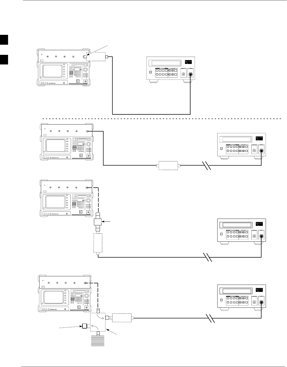
Manual Cable Calibration – continued
B-38 1X SC480 BTS Hardware Installation, Optimization/ATP, and FRU MAY 2004
PRELIMINARY
Figure B-24: Cable Calibration Using Advantest R3465
POWER
SENSOR
20 DB / 2 WATT
ATTENUATOR
(A)
(C)
POWER
SENSOR
(D)
30 DB
DIRECTIONAL
COUPLER
(C)
100 W
NON–RADIATING
RF LOAD
POWER
SENSOR
RF OUT
POWER
SENSOR
& (B)
FW00320
50 Ω
TERMINATION
B

MAY 2004 1X SC480 BTS Hardware Installation, Optimization/ATP, and FRU
PRELIMINARY
Appendix C: Download ROM Code
Appendix Content
Downloading ROM Code C-1 . . . . . . . . . . . . . . . . . . . . . . . . . . . . . . . . . . . . . . . . . .
Exception Procedure – Downloading ROM Code C-1 . . . . . . . . . . . . . . . . .
C

Table of Contents – continued
1X SC480 BTS Hardware Installation, Optimization/ATP, and FRU MAY 2004
PRELIMINARY
Notes
C
Downloading ROM Code
MAY 2004 1X SC480 BTS Hardware Installation, Optimization/ATP, and FRU C-1
PRELIMINARY
Exception Procedure –
Downloading ROM Code
This procedure is not part of a normal optimization.
Perform this procedure only on an exception basis when no alternative
exists to load a BTS device with the correct version of ROM code.
One GLI must be INS_ACT (bright green) before ROM
code can be downloaded to non–GLI devices.
NOTE
The correct ROM and RAM codes for the software release
used on the BSS must be loaded into BTS devices. To
identify the correct device ROM and RAM code loads for
the software release being used on the BSS, refer to the
Version Matrix section of the SCt CDMA Release Notes
(supplied on the tapes or CD–ROMs containing the BSS
software).
All devices in a BTS must be loaded with the ROM and
RAM code specified for the software release used on the
BSS before any optimization or ATP procedures can be
performed.
If a replacement device is loaded with ROM code which is
not compatible with the BSS software release being used,
the device ROM code can be changed using the LMF
before performing the BTS optimization and ATPs. A
device loaded with later release ROM code can not be
converted back to a previous release ROM code in the field
without Motorola assistance
CAUTION
If it is necessary to download ROM code to a device from the LMF, the
procedure in Table C-1 includes steps for both ROM and RAM code
download using the LMF.
Prerequisites
Prior to performing this procedure, ensure the correct ROM and RAM
code files exist in the LMF computer’s applicable <x>:\<lmf home
directory>\cdma\loads\<codeload#>\code folder for each of the devices
to be loaded.
C

Downloading ROM Code – continued
C-2 1X SC480 BTS Hardware Installation, Optimization/ATP, and FRU MAY 2004
PRELIMINARY
The Release level of the ROM code to be downloaded
must be the one specified for the software release installed
in the BSS. The release level of the ROM code resident in
the other devices in the BTS must also be correct for the
BSS software release being used. ROM code must not be
downloaded to a frame loaded with code for a BSS
software release with which it is not compatible.
This procedure should only be used to upgrade
replacement devices for a BTS. It should NOT be used to
upgrade all devices in a BTS. If a BTS is to be upgraded
from R15.x to R16.0, the upgrade should be done by the
OMC–R using the DownLoad Manager.
CAUTION
Table C-1: Download ROM and RAM Code to Devices
Step Action
1Click on the device to be loaded.
NOTE
More than one device of the same type can be selected for download by either clicking on each one to
be downloaded or from the BTS menu bar Select pull–down menu, select the device item that applies.
Where: device = the type of device to be loaded (BBX, CSA, GLI, MCC)
2From the BTS menu bar Device pull–down menu, select Status.
– A status report window will appear.
3Make a note of the number in the HW Bin Type column.
NOTE
“HW Bin Type” is the Hardware Binary Type for the device. This code is used as the last four digits in
the filename of a device’s binary ROM code file. Using this part of the filename, the ROM code file
can be matched to the device in which it is to be loaded.
4 Click OK to close the status window.
5Click on the device to be loaded.
NOTE
ROM code is automatically selected for download from the <x>:\<lmf home
directory>\version folder>\<code folder> specified by the NextLoad property in
the bts–#.cdf file. To check the value of the NextLoad property, click on Util > Examine >
Display Nextload. A pop–up message will show the value of the NextLoad.
6From the BTS menu bar Device pull–down menus, select Download > ROM.
– If the file matching the Hardware Binary Type of the device is found in the code folder, a status
report shows the result of the download. Proceed to Step 11.
– If a file selection window appears, select the ROM code file manually.
7Double–click on the version folder with the desired version number for the ROM code file (for
example 2.16.0.x).
. . . continued on next page
C

Downloading ROM Code – continued
MAY 2004 1X SC480 BTS Hardware Installation, Optimization/ATP, and FRU C-3
PRELIMINARY
Table C-1: Download ROM and RAM Code to Devices
Step Action
8Double–click the Code folder.
– A list of ROM and RAM code files will be displayed.
9! CAUTION
A ROM code file with the correct HW Bin Type must be chosen. Using a file with the wrong HW Bin
Type can result in unpredictable operation and damage to the device.
Click on the ROM code file with the filename which matches the device type and HW Bin Type
number noted in step 3 (for example, file bbx_rom.bin.0604 is the ROM code file for a BBX with a
HW Bin Type of 0604).
– The file should be highlighted.
10 Click on the Load button.
– A status report window is displayed showing the result of the download.
NOTE
If the ROM load failed for some devices, load them individually by clicking on one device, perform
steps 6 through 10 for it, and repeat the process for each remaining device.
11 Click OK to close the status window.
12 From the LMF window menu bar Tools pull–down menus, select Update NextLoad > CDMA.
13 In the left–hand pane of the window which opens, click on the BTS number for the frame being loaded
(for example, BTS–14).
14 On the list of versions displayed in the right–hand pane, click the button next to the version number of
the folder that was used for the ROM code download (for example, 2.16.0.x) and click Save.
– A pop–up message will appear showing the CDF has been updated.
15 Click on the OK button to dismiss the pop–up message.
16 Click on the device that was loaded with ROM code.
17 NOTE
RAM code is automatically selected for download.
From the BTS menu bar Device pull–down menus, select Download > Code/Data to download RAM
code and dds file data.
– A status report is displayed showing the result of the download.
18 Click OK to close the status window.
19 Observe the downloaded non–GLI device to ensure it is OOS_RAM (yellow).
20 Click on the device which was loaded with code.
21 From the BTS menu bar Device pull–down menu, select Status.
Verify that the correct ROM and RAM version numbers are displayed in the status report window.
22 Click OK to close the status window.
C

Downloading ROM Code – continued
C-4 1X SC480 BTS Hardware Installation, Optimization/ATP, and FRU MAY 2004
PRELIMINARY
Notes
C

MAY 2004 1X SC480 BTS Hardware Installation, Optimization/ATP, and FRU
PRELIMINARY
Appendix D: MMI Cable Fabrication
Appendix Content
MMI Cable Fabrication D-1 . . . . . . . . . . . . . . . . . . . . . . . . . . . . . . . . . . . . . . . . . . .
Purpose D-1 . . . . . . . . . . . . . . . . . . . . . . . . . . . . . . . . . . . . . . . . . . . . . . . . .
Required Parts D-1 . . . . . . . . . . . . . . . . . . . . . . . . . . . . . . . . . . . . . . . . . . . .
Cable Details D-1 . . . . . . . . . . . . . . . . . . . . . . . . . . . . . . . . . . . . . . . . . . . . .
Wire Run List D-2 . . . . . . . . . . . . . . . . . . . . . . . . . . . . . . . . . . . . . . . . . . . . . D

Table of Contents – continued
1X SC480 BTS Hardware Installation, Optimization/ATP, and FRU MAY 2004
PRELIMINARY
Notes
D
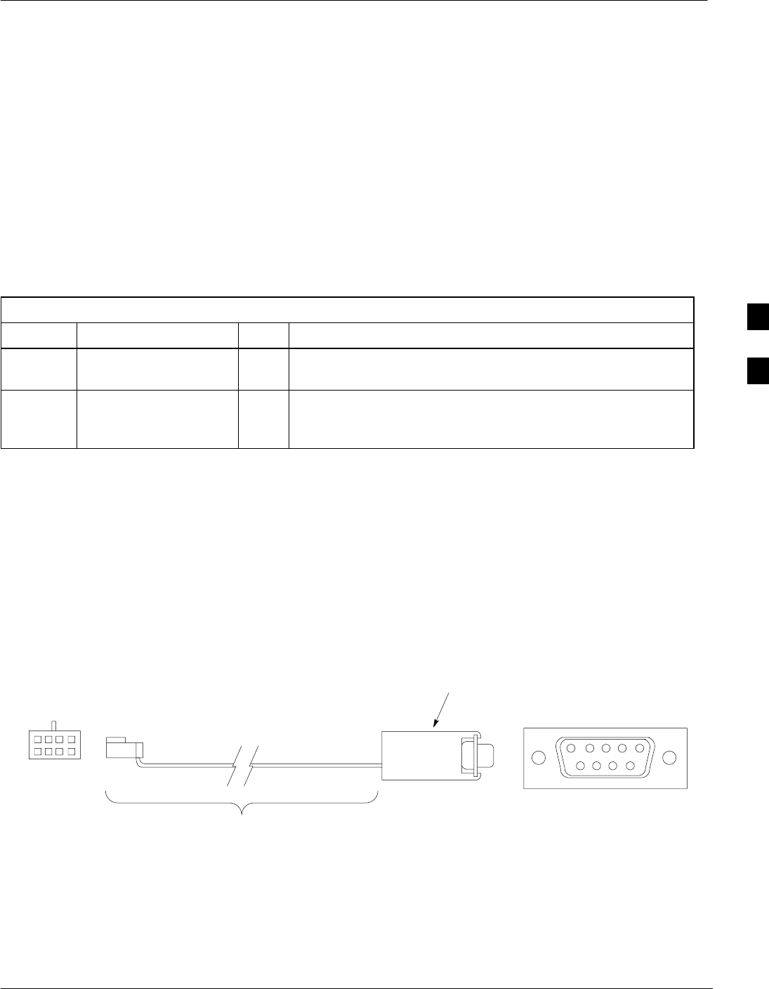
MMI Cable Fabrication
MAY 2004 1X SC480 BTS Hardware Installation, Optimization/ATP, and FRU D-1
PRELIMINARY
Purpose
When the Motorola SLN2006A MMI Interface Kit is not available, a
cable can be fabricated by the user to interface a nine–pin serial
connector on an LMF computer platform with an MMI connector on
GLI cards and other Motorola BTS assemblies. This section provides
information necessary for fabricating this cable.
Required Parts
Table D-1: Parts Required to Fabricate MMI Cable
Item Part Number Qty Description
AMotorola 3009786R01 1Ribbon cable assembly, 1.524 M, one 8–contact MMI
connector, one 10–contact connector
BAMP 749814–1,
Belkin A4B202BGC,
or equivalent
1Receptacle kit, unassembled, 9–position, socket contacts,
unshielded, metal or plastic shell, solder or crimp–type
contacts
Cable Details
Figure D-1 illustrates the details of the fabricated MMI cable.
Figure D-1: Fabricated MMI Cable Details
DB–9 Plug
Socket Numbering
(Mating Side)
12345
6789
1
2
3
4
5
6
7
8
8–Contact MMI Plug
Socket Numbering
(Mating Side)
Item A: Cable assembly 3009786R01 (with 10–contact plug removed)
MMIFAB001–0
FABRICATION NOTES:
1. Remove 10–contact connector from ribbon cable of cable assembly 3009786R01
2. Separate wires at unterminated end of ribbon cable as required to connect to DB–9
connector contacts
3. Dark wire on ribbon cable of cable assembly 3009786R01 connects to pin 1 of the
8–contact plug
4. Strip three ribbon cable wires with connections specified in Table D-2 and connect to
DB–9 plug contacts as specified in Table D-2
5. Shorten un–connected ribbon cable wires enough to prevent contacting DB–9
contacts, leaving enough wire to egage any strain relief in the DB–9 connector shell
Item B
D

MMI Cable Fabrication – continued
D-2 1X SC480 BTS Hardware Installation, Optimization/ATP, and FRU MAY 2004
PRELIMINARY
Wire Run List
Table D-2 provides the wire run/pin–out information for the fabricated
MMI cable.
Table D-2: Fabricated MMI Cable Wire Run List
8–CONTACT MMI
PLUG CONTACT DB–9 PLUG
CONTACT
1 ––––––––––––––––– 5
2 ––––––––––––––––– 2
3 ––––––––––––––––– 3
4No Connection (NC)
5 NC
6 NC
7 NC
8 NC
D

MAY 2004 1X SC480 BTS Hardware Installation, Optimization/ATP, and FRU
PRELIMINARY
Appendix E: Multiple BTS Configurations
Appendix Content
Compact BTS Expansion Configuration (Indoor) E-1 . . . . . . . . . . . . . . . . . . . . . . .
Introduction E-1 . . . . . . . . . . . . . . . . . . . . . . . . . . . . . . . . . . . . . . . . . . . . . .
Materials Needed E-1 . . . . . . . . . . . . . . . . . . . . . . . . . . . . . . . . . . . . . . . . . .
External Combiner and Directional Coupler E-1 . . . . . . . . . . . . . . . . . . . . .
Frame ID Switch Settings E-2 . . . . . . . . . . . . . . . . . . . . . . . . . . . . . . . . . . .
Installation Procedure for Expansion Compact BTS with Dual
cCLPAs E-2 . . . . . . . . . . . . . . . . . . . . . . . . . . . . . . . . . . . . . . . . . . . . . . . . .
Starter and Three Expansion BTSes Interconnect Cabling for
Dual cCLPA E-3 . . . . . . . . . . . . . . . . . . . . . . . . . . . . . . . . . . . . . . . . . . . . . .
Starter and Two Expansion BTSes Interconnect Cabling for
Dual cCLPA E-5 . . . . . . . . . . . . . . . . . . . . . . . . . . . . . . . . . . . . . . . . . . . . . .
Starter and One Expansion BTSes Interconnect Cabling for
Dual cCLPA E-7 . . . . . . . . . . . . . . . . . . . . . . . . . . . . . . . . . . . . . . . . . . . . . .
Installation Procedure for Expansion Compact BTS with
Single cCLPA E-9 . . . . . . . . . . . . . . . . . . . . . . . . . . . . . . . . . . . . . . . . . . . .
Starter and Three Expansion BTSes Interconnect Cabling for
Single cCLPA E-10 . . . . . . . . . . . . . . . . . . . . . . . . . . . . . . . . . . . . . . . . . . . .
Starter and Two Expansion BTSes Interconnect Cabling for
Single cCLPA E-12 . . . . . . . . . . . . . . . . . . . . . . . . . . . . . . . . . . . . . . . . . . . .
Starter and One Expansion BTSes Interconnect Cabling for
Single cCLPA E-14 . . . . . . . . . . . . . . . . . . . . . . . . . . . . . . . . . . . . . . . . . . . .
Installation Procedure for Expansion Compact BTS without
cCLPA E-16 . . . . . . . . . . . . . . . . . . . . . . . . . . . . . . . . . . . . . . . . . . . . . . . . . .
Starter and Expansion BTSes Interconnect Cabling without
cCLPA E-16 . . . . . . . . . . . . . . . . . . . . . . . . . . . . . . . . . . . . . . . . . . . . . . . . . .
Starter and Two Expansion BTSes to cCLPA Cabling E-20 . . . . . . . . . . . . .
Starter and One Expansion BTS to cCLPA Cabling E-21 . . . . . . . . . . . . . . .
Multiple Compact BTS Configuration (Outdoor) E-22 . . . . . . . . . . . . . . . . . . . . . . .
Introduction E-22 . . . . . . . . . . . . . . . . . . . . . . . . . . . . . . . . . . . . . . . . . . . . . .
Materials Needed E-22 . . . . . . . . . . . . . . . . . . . . . . . . . . . . . . . . . . . . . . . . . .
External Combiner and Directional Coupler E-22 . . . . . . . . . . . . . . . . . . . . .
ExpansionCompact BTS Installation Procedure E-23 . . . . . . . . . . . . . . . . . .
Frame ID Switch Settings E-23 . . . . . . . . . . . . . . . . . . . . . . . . . . . . . . . . . . .
Other Diagrams E-26 . . . . . . . . . . . . . . . . . . . . . . . . . . . . . . . . . . . . . . . . . . .
E

Table of Contents – continued
1X SC480 BTS Hardware Installation, Optimization/ATP, and FRU MAY 2004
PRELIMINARY
Notes
E

Compact BTS Expansion Configuration (Indoor)
MAY 2004 1X SC480 BTS Hardware Installation, Optimization/ATP, and FRU E-1
PRELIMINARY
Introduction
This appendix covers the indoor and outdoor version of the Compact
BTS Expansion configuration. This configuration is set up for only
using other Compact BTSes. Power and ground cabling is not shown.
Figure E-1 through Figure E-3 show expansion BTSes using two
cCLPAs.
Figure E-4 through Figure E-6 show expansion BTSes using one
cCLPA.
Materials Needed
The following materials are required to configure expansion BTSes.
SInterconnect cabling of varying lengths
SVarious sized conduit (if used)
SData cable for cCLPA (if used)
SCustomer I/O cabling
External Combiner and
Directional Coupler
A combiner and directional coupler are required for some of the
configurations. The following are the recommended specifications for
the combiner and directional coupler.
Table E-1: Combiner and Directional Coupler Specifications
Item Specifications
Combiner
Connector: N–Type
Frequency Range: Up to 2 GHz
Insertion Loss: 3.5 dB maximum
Return Loss: 16 dB minimum
Average Input Power: 60 Watts minimum
Directional Coupler
Connector: N–Type
Frequency Range: 810 to 950 MHz
Coupling: 30 +/–1 dB
Directivity: 28 dB minimum
Return Loss: 18 dB minimum
Average Input Power: 10 Watts minimum
E

Compact BTS Expansion Configuration (Indoor) – continued
E-2 1X SC480 BTS Hardware Installation, Optimization/ATP, and FRU MAY 2004
PRELIMINARY
SMotorola recommended directional coupler is P/N 809643T03
SRecommended cable with combiner is Andrew LDF4–50 or
equivalent
Frame ID Switch Settings
Refer to Chapter 5, Figure 5-1 or Figure 5-2 or Table 5-1 through
Table 5-4 for the Frame DIP Switch settings.
Installation Procedure for
Expansion Compact BTS with
Dual cCLPAs
Follow the procedure in Table E-2 for installation of expansion Compact
BTS with Dual cCLPAs.
Table E-2: Procedure for Installing Expansion Compact BTS with Dual cCLPA
Step Action
1Follow the procedure in Chapter 4 for installing a Compact BTS in a rack.
2For a 3 BTS expansion configuration, follow Figure E-1. Proceed to step 3.
2a For a 2 BTS expansion configuration, follow Figure E-2. Proceed to step 3.
2b For a 1 BTS expansion configuration, follow Figure E-3. Proceed to step 3.
3If not using conduit, dress cables as necessary.
4Perform Optimization and ATP as described in Chapter 6. LMF Help provides further information.
E

Compact BTS Expansion Configuration (Indoor) – continued
MAY 2004 1X SC480 BTS Hardware Installation, Optimization/ATP, and FRU E-3
PRELIMINARY
Starter and Three Expansion
BTSes Interconnect Cabling for
Dual cCLPA
Table E-3 shows in tabular format the interconnect cabling of
Figure E-1.
Table E-3: Starter and Three Expansion BTS Interconnect Cabling
for Circuit or Packet Configuration with Dual cCLPA
BTS Expansion 1 Expansion 2 Expansion 3 cCLPA
Starter TX–1 –––cCLPA–1 (TX IN)
Starter TX–2 –––cCLPA–2 (TX IN)
Starter EXP–TX 2 EXP TX–2 – – *cCLPA–2
Starter EXP–TX 3 –EXP TX–2 – *cCLPA–1
Starter EXP–TX 4 – – EXP TX–2 *cCLPA–2
Starter RX MAIN – – – cCLPA–1
(RX OUT)
Starter EXP–RX MAIN 2 –EXP – RX
MAIN 2 – *cCLPA–1
Starter EXP–RX MAIN 3 EXP – RX
MAIN 2 – – *cCLPA–2
Starter EXP–RX MAIN 4 – – EXP – RX
MAIN 2 *cCLPA–2
Starter RX DIV – – – cCLPA–2
(RX OUT)
Starter EXP–RX DIV 2 EXP – RX DIV
2– – *cCLPA–2
Starter EXP–RX DIV 3 –EXP – RX DIV
2– *cCLPA–1
Starter EXP–RX DIV 4 – – EXP – RX DIV
2*cCLPA–2
Starter SDCX 2 SDC INPUT
EXPANSION – – –
Starter SDCX 3 –SDC INPUT
EXPANSION – –
Starter SDCX 4 – – SDC INPUT
EXPANSION –
* Not actual physical connections to cCLPA, but software connections through the Starter BTS.
E
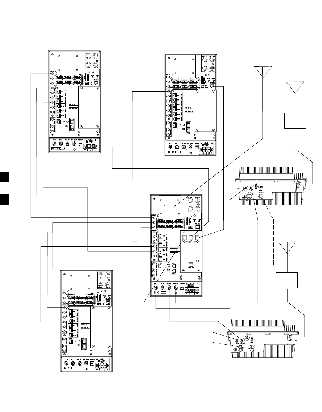
Compact BTS Expansion Configuration (Indoor) – continued
E-4 1X SC480 BTS Hardware Installation, Optimization/ATP, and FRU MAY 2004
PRELIMINARY
Figure E-1: Three Expansion BTSes Cabling Diagram with Two cCLPAs
EXPANSION 3
EXPANSION 2
EXPANSION 1
STARTER
cCLPA 1
cCLPA 2
LOCAL GPS
Power and Ground not shown
LA
LA
Ensure that the expansion
BTSes have an Expansion
cMPC card installed.
E

Compact BTS Expansion Configuration (Indoor) – continued
MAY 2004 1X SC480 BTS Hardware Installation, Optimization/ATP, and FRU E-5
PRELIMINARY
Starter and Two Expansion
BTSes Interconnect Cabling for
Dual cCLPA
Table E-4 shows in tabular format the interconnect cabling of
Figure E-2.
Table E-4: Starter and Two Expansion BTS Interconnect Cabling
for Circuit or Packet Configuration with Dual cCLPA
BTS Expansion 1 Expansion 2 Expansion 3 cCLPA
Starter TX–1 –––cCLPA–1 (TX IN)
Starter TX–2 –––cCLPA–2 (TX IN)
Starter EXP–TX 2 EXP TX–2 – – *cCLPA–2
Starter EXP–TX 3 –EXP TX–2 – *cCLPA–1
Starter EXP–TX 4 – – – –
Starter RX MAIN – – – cCLPA–1
(RX OUT)
Starter EXP–RX MAIN 2 EXP – RX
MAIN 2 – *cCLPA–1
Starter EXP–RX MAIN 3 EXP – RX
MAIN 2 – *cCLPA–2
Starter EXP–RX MAIN 4 – – – –
Starter RX DIV – – – cCLPA–2
(RX OUT)
Starter EXP–RX DIV 2 EXP – RX
DIV 2 – – *cCLPA–2
Starter EXP–RX DIV 3 –EXP – RX
DIV 2 – *cCLPA–1
Starter EXP–RX DIV 4 – – – –
Starter SDCX 2 SDC INPUT
EXPANSION – – –
Starter SDCX 3 –SDC INPUT
EXPANSION – –
Starter SDCX 4 – – – –
* Not actual physical connections to cCLPA, but software connections through the Starter BTS.
E
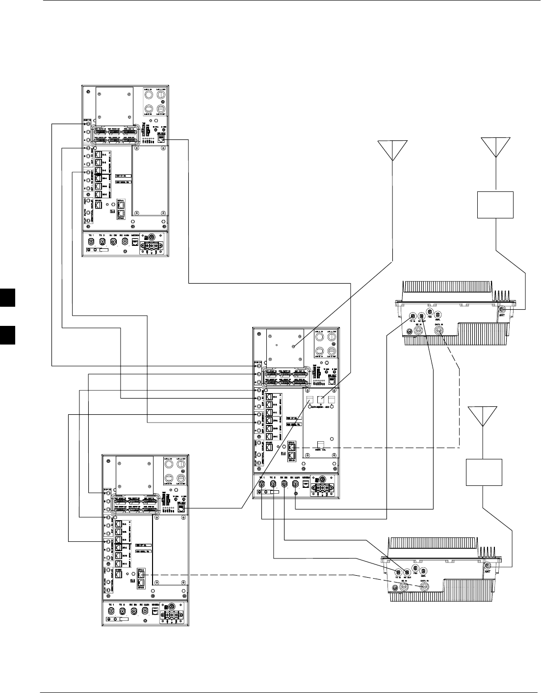
Compact BTS Expansion Configuration (Indoor) – continued
E-6 1X SC480 BTS Hardware Installation, Optimization/ATP, and FRU MAY 2004
PRELIMINARY
Figure E-2: Two Expansion BTSes Cabling Diagram with Two cCLPAs
EXPANSION 2
EXPANSION 1
STARTER
cCLPA 1
cCLPA 2
LOCAL GPS
Power and Ground not shown
LA
LA
Ensure that the expansion
BTSes have an Expansion
cMPC card installed.
E

Compact BTS Expansion Configuration (Indoor) – continued
MAY 2004 1X SC480 BTS Hardware Installation, Optimization/ATP, and FRU E-7
PRELIMINARY
Starter and One Expansion
BTSes Interconnect Cabling for
Dual cCLPA
Table E-5 shows in tabular format the interconnect cabling of
Figure E-3.
Table E-5: Starter and One Expansion BTS Interconnect Cabling
for Circuit or Packet Configuration with Dual cCLPA
BTS Expansion 1 Expansion 2 Expansion 3 cCLPA
Starter TX–1 –––cCLPA–1 (TX IN)
Starter TX–2 –––cCLPA–2 (TX IN)
Starter EXP–TX 2 EXP TX–2 – – –
Starter EXP–TX 3 – – – –
Starter EXP–TX 4 – – – –
Starter RX MAIN – – – cCLPA–1
(RX OUT)
Starter EXP–RX MAIN 2 – – – –
Starter EXP–RX MAIN 3 EXP – RX
MAIN 2 – – *cCLPA–2
Starter EXP–RX MAIN 4 – – – –
Starter RX DIV – – – cCLPA–2
(RX OUT)
Starter EXP–RX DIV 2 EXP – RX
DIV 2 – – *cCLPA–2
Starter EXP–RX DIV 3 – – – –
Starter EXP–RX DIV 4 – – – –
Starter SDCX 2 SDC INPUT
EXPANSION – – –
Starter SDCX 3 – – – –
Starter SDCX 4 – – – –
* Not actual physical connections to cCLPA, but software connections through the Starter BTS.
E
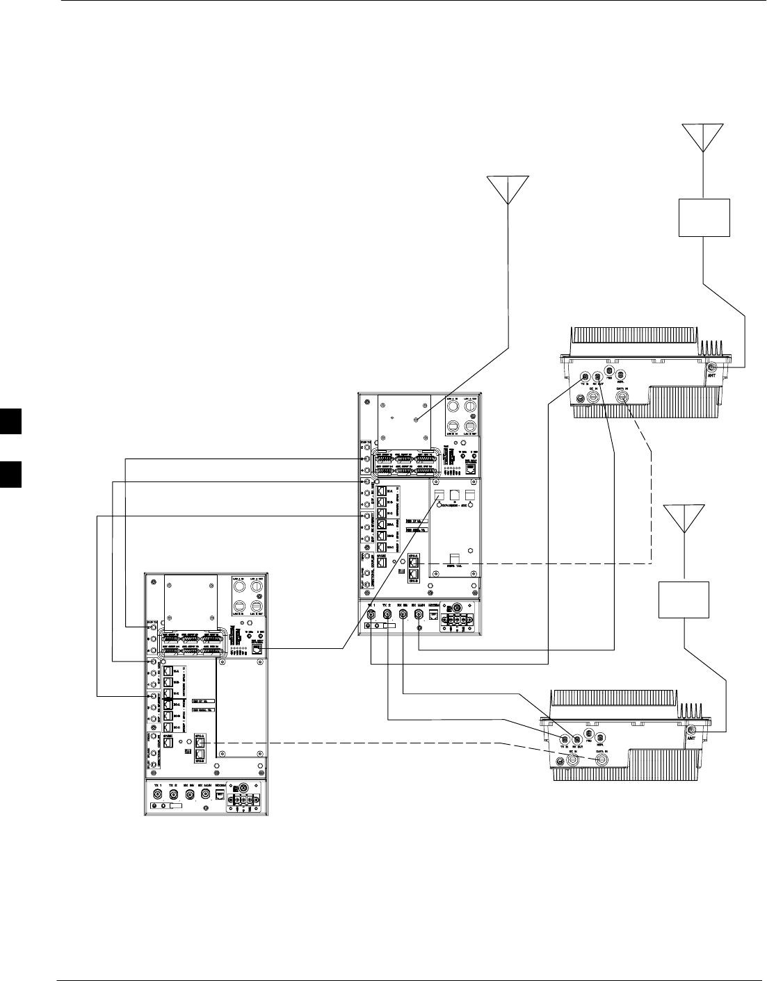
Compact BTS Expansion Configuration (Indoor) – continued
E-8 1X SC480 BTS Hardware Installation, Optimization/ATP, and FRU MAY 2004
PRELIMINARY
LA
LA
EXPANSION 1
STARTER
cCLPA 1
cCLPA 2
LOCAL GPS
Figure E-3: One Expansion BTS Cabling Diagram with Two cCLPAs
Power and Ground not shown
Ensure that the expansion
BTS has an Expansion cMPC
card installed.
E

Compact BTS Expansion Configuration (Indoor) – continued
MAY 2004 1X SC480 BTS Hardware Installation, Optimization/ATP, and FRU E-9
PRELIMINARY
Installation Procedure for
Expansion Compact BTS with
Single cCLPA
Follow the procedure in Table E-2 for installation of expansion Compact
BTS with Dual cCLPAs.
Table E-6: Procedure for Installing Expansion Compact BTS with Single cCLPA
Step Action
1Follow the procedure in Chapter 4 for installing a Compact BTS in a rack.
2For a 3 BTS expansion configuration, follow Figure E-4. Proceed to step 3.
2a For a 2 BTS expansion configuration, follow Figure E-5. Proceed to step 3.
2b For a 1 BTS expansion configuration, follow Figure E-6. Proceed to step 3.
3If not using conduit, dress cables as necessary.
4Perform Optimization and ATP as described in Chapter 6. LMF Help provides further information.
E

Compact BTS Expansion Configuration (Indoor) – continued
E-10 1X SC480 BTS Hardware Installation, Optimization/ATP, and FRU MAY 2004
PRELIMINARY
Starter and Three Expansion
BTSes Interconnect Cabling for
Single cCLPA
Table E-7 shows in tabular format the interconnect cabling of
Figure E-4.
Table E-7: Starter and Three Expansion BTS Interconnect Cabling
for Circuit or Packet Configuration with Single cCLPA
BTS Expansion 1 Expansion 2 Expansion 3 cCLPA
Starter TX–1 Signals are sent thruogh an external combiner and
directional coupler
cCLPA–1 (TX IN)
Starter TX–2
directional coupler
Starter EXP–TX 2 EXP TX–2 – – *cCLPA–1
Starter EXP–TX 3 –EXP TX–2 – *cCLPA–1
Starter EXP–TX 4 – – EXP TX–2 *cCLPA–1
Starter RX MAIN – – – Antenna
Starter EXP–RX MAIN 2 EXP – RX
MAIN 2 – – *cCLPA–1
Starter EXP–RX MAIN 3 –EXP – RX
MAIN 2 – *cCLPA–1
Starter EXP–RX MAIN 4 – – EXP – RX
MAIN 2 *cCLPA–1
Starter RX DIV – – – cCLPA–1
(RX OUT)
Starter EXP–RX DIV 2 EXP – RX DIV
2– – *cCLPA–1
Starter EXP–RX DIV 3 –EXP – RX DIV
2– *cCLPA–1
Starter EXP–RX DIV 4 – – EXP – RX DIV
2*cCLPA–1
Starter SDCX 2 SDC INPUT
EXPANSION – – –
Starter SDCX 3 –SDC INPUT
EXPANSION – –
Starter SDCX 4 – – SDC INPUT
EXPANSION –
* Not actual physical connections to cCLPA, but software connections through the Starter BTS.
E
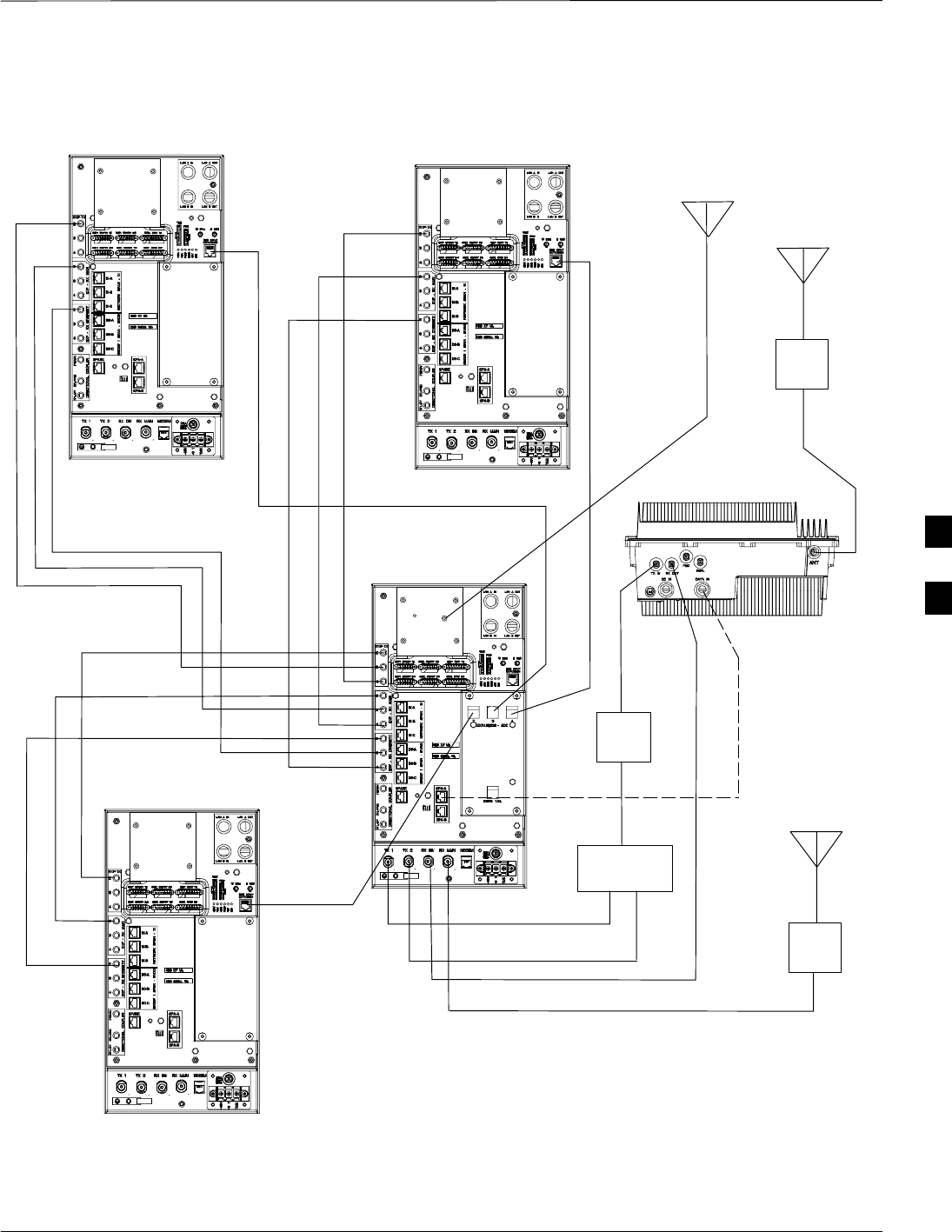
Compact BTS Expansion Configuration (Indoor) – continued
MAY 2004 1X SC480 BTS Hardware Installation, Optimization/ATP, and FRU E-11
PRELIMINARY
Figure E-4: Three Expansion BTSes Cabling Diagram with One cCLPA
EXPANSION 3
EXPANSION 2
EXPANSION 1
STARTER
cCLPA 1
LOCAL GPS
Power and Ground not shown
COMBINER
LA
LA
RX DIV
RX MAIN
TX 1
TX 2
DC
Ensure that the expansion
BTSes have an Expansion
cMPC card installed.
E

Compact BTS Expansion Configuration (Indoor) – continued
E-12 1X SC480 BTS Hardware Installation, Optimization/ATP, and FRU MAY 2004
PRELIMINARY
Starter and Two Expansion
BTSes Interconnect Cabling for
Single cCLPA
Table E-8 shows in tabular format the interconnect cabling of
Figure E-5.
Table E-8: Starter and Two Expansion BTS Interconnect Cabling
for Circuit or Packet Configuration with Single cCLPA
BTS Expansion 1 Expansion 2 Expansion 3 cCLPA
Starter TX–1 Signals are sent thruogh an external combiner and
directional coupler
cCLPA–1 (TX IN)
Starter TX–2
directional coupler
Starter EXP–TX 2 EXP TX–2 – – *cCLPA–1
Starter EXP–TX 3 –EXP TX–2 – *cCLPA–1
Starter EXP–TX 4 – – – –
Starter RX MAIN – – – Antenna
Starter EXP–RX MAIN 2 EXP – RX
MAIN 2 – – *cCLPA–1
Starter EXP–RX MAIN 3 –EXP – RX
MAIN 2 – *cCLPA–1
Starter EXP–RX MAIN 4 – – – –
Starter RX DIV – – – cCLPA–1
(RX OUT)
Starter EXP–RX DIV 2 EXP – RX
DIV 2 – – *cCLPA–1
Starter EXP–RX DIV 3 –EXP – RX
DIV 2 – *cCLPA–1
Starter EXP–RX DIV 4 – – – –
Starter SDCX 2 SDC INPUT
EXPANSION – – –
Starter SDCX 3 –SDC INPUT
EXPANSION – –
Starter SDCX 4 – – – –
* Not actual physical connections to cCLPA, but software connections through the Starter BTS.
E
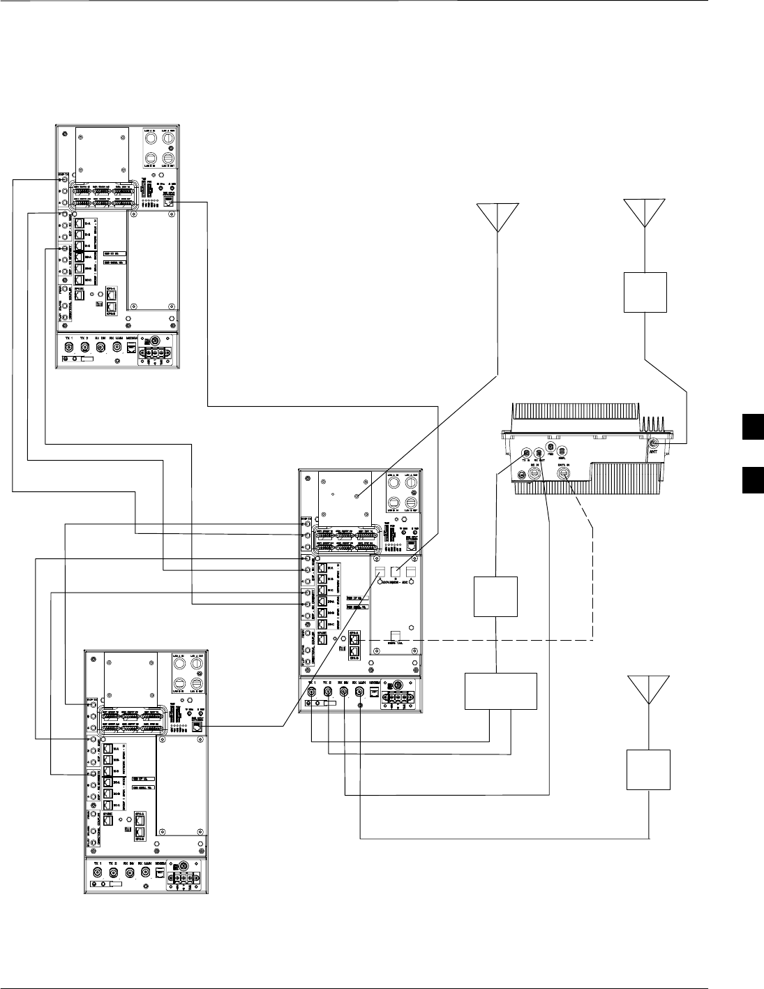
Compact BTS Expansion Configuration (Indoor) – continued
MAY 2004 1X SC480 BTS Hardware Installation, Optimization/ATP, and FRU E-13
PRELIMINARY
Figure E-5: Two Expansion BTSes Cabling Diagram with One cCLPA
LA
EXPANSION 2
EXPANSION 1
STARTER
cCLPA 1
LOCAL GPS
Power and Ground not shown
COMBINER
LA
RX DIV
RX MAIN
TX 1
TX 2
DC
Ensure that the expansion
BTSes have an Expansion
cMPC cards installed.
E

Compact BTS Expansion Configuration (Indoor) – continued
E-14 1X SC480 BTS Hardware Installation, Optimization/ATP, and FRU MAY 2004
PRELIMINARY
Starter and One Expansion
BTSes Interconnect Cabling for
Single cCLPA
Table E-9 shows in tabular format the interconnect cabling of
Figure E-6.
Table E-9: Starter and One Expansion BTS Interconnect Cabling
for Circuit or Packet Configuration with Single cCLPA
BTS Expansion 1 Expansion 2 Expansion 3 cCLPA
Starter TX–1 –––cCLPA–1 (TX IN)
Starter TX–2 – – – –
Starter EXP–TX 2 EXP TX–2 – – –
Starter EXP–TX 3 – – – –
Starter EXP–TX 4 – – – –
Starter RX MAIN – – – Antenna
Starter EXP–RX MAIN 2 – – – –
Starter EXP–RX MAIN 3 EXP – RX
MAIN 2 – – *cCLPA–1
Starter EXP–RX MAIN 4 – – – –
Starter RX DIV – – – cCLPA–1
(RX OUT)
Starter EXP–RX DIV 2 EXP – RX
DIV 2 – – *cCLPA–1
Starter EXP–RX DIV 3 – – – –
Starter EXP–RX DIV 4 – – – –
Starter SDCX 2 SDC INPUT
EXPANSION – – –
Starter SDCX 3 – – – –
Starter SDCX 4 – – – –
* Not actual physical connections to cCLPA, but software connections through the Starter BTS.
E
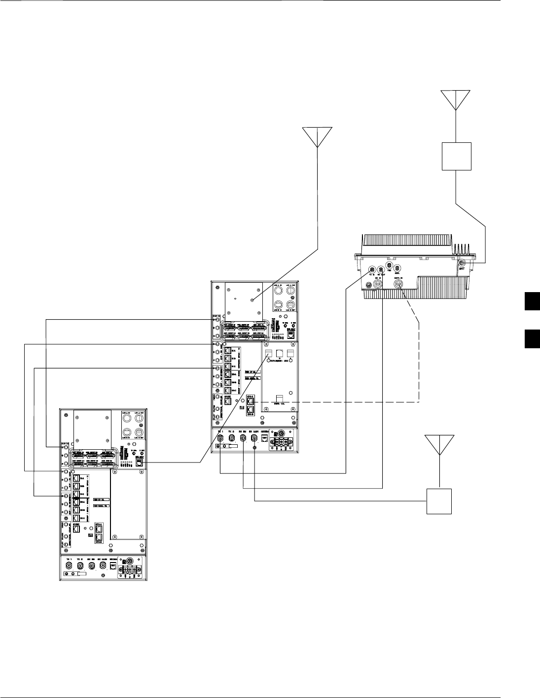
Compact BTS Expansion Configuration (Indoor) – continued
MAY 2004 1X SC480 BTS Hardware Installation, Optimization/ATP, and FRU E-15
PRELIMINARY
LA
EXPANSION 1
STARTER
cCLPA 1
LOCAL GPS
Figure E-6: One Expansion BTS Cabling Diagram with One cCLPA
Power and Ground not shown
Ensure that the expansion
BTS has an Expansion cMPC
card installed.
LA
RX MAIN
RX DIV
TX 1
E

Compact BTS Expansion Configuration (Indoor) – continued
E-16 1X SC480 BTS Hardware Installation, Optimization/ATP, and FRU MAY 2004
PRELIMINARY
Installation Procedure for
Expansion Compact BTS
without cCLPA
Follow the procedure in Table E-2 for installation of expansion Compact
BTS without cCLPAs. Table E-7 through Table E-9 (less the cCLPA) are
virtually the same and are can be used for the diagrams without cCLPA,
and so separate tables will not be included here.
Table E-10: Procedure for Installing Expansion Compact BTS without cCLPA
Step Action
1Follow the procedure in Chapter 4 for installing a Compact BTS in a rack.
2For a 3 BTS expansion configuration, follow Figure E-7. Proceed to step 3.
2a For a 2 BTS expansion configuration, follow Figure E-8. Proceed to step 3.
2b For a 1 BTS expansion configuration, follow Figure E-9. Proceed to step 3.
3If not using conduit, dress cables as necessary.
4Perform Optimization and ATP as described in Chapter 6. LMF Help provides further information.
Starter and Expansion BTSes
Interconnect Cabling without
cCLPA
Table E-7 through Table E-9 are virtually the same and are can be used
for the diagrams without cCLPA. Separate tables will not be included
here.
E
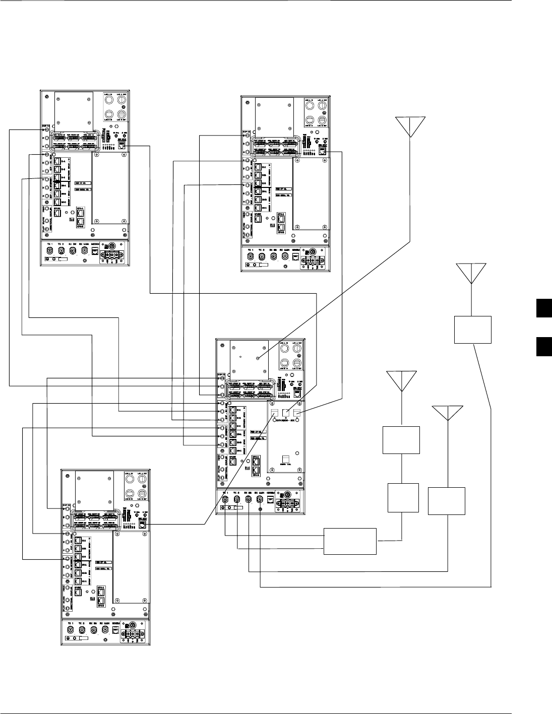
Compact BTS Expansion Configuration (Indoor) – continued
MAY 2004 1X SC480 BTS Hardware Installation, Optimization/ATP, and FRU E-17
PRELIMINARY
Figure E-7: Three Expansion BTSes Cabling Diagram
EXPANSION 3
EXPANSION 2
EXPANSION 1
STARTER
LOCAL GPS
Power and Ground not shown
COMBINER
RX MAIN
RX DIV
TX 1
TX 2
LA
LA
LA
DC
Ensure that the expansion
BTSes have the expansion
cMPC cards installed.
E
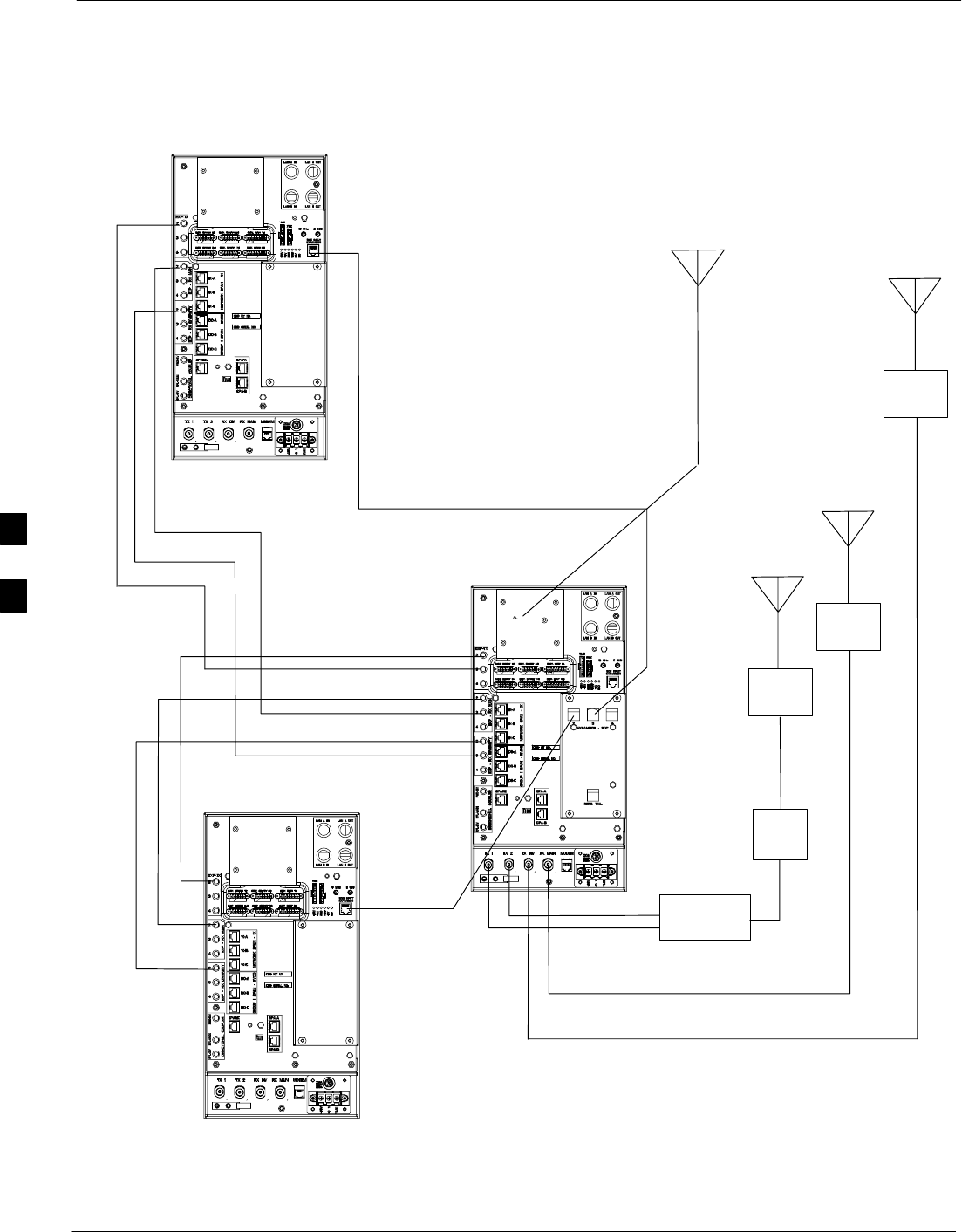
Compact BTS Expansion Configuration (Indoor) – continued
E-18 1X SC480 BTS Hardware Installation, Optimization/ATP, and FRU MAY 2004
PRELIMINARY
Figure E-8: Two Expansion BTSes Cabling Diagram
EXPANSION 2
EXPANSION 1
STARTER
LOCAL GPS
Power and Ground not shown
Ensure that the expansion
BTSes have the expansion
cMPC cards installed.
COMBINER
TX 1
RX MAIN
RX DIV
TX 2
DC
LA
LA
LA
E
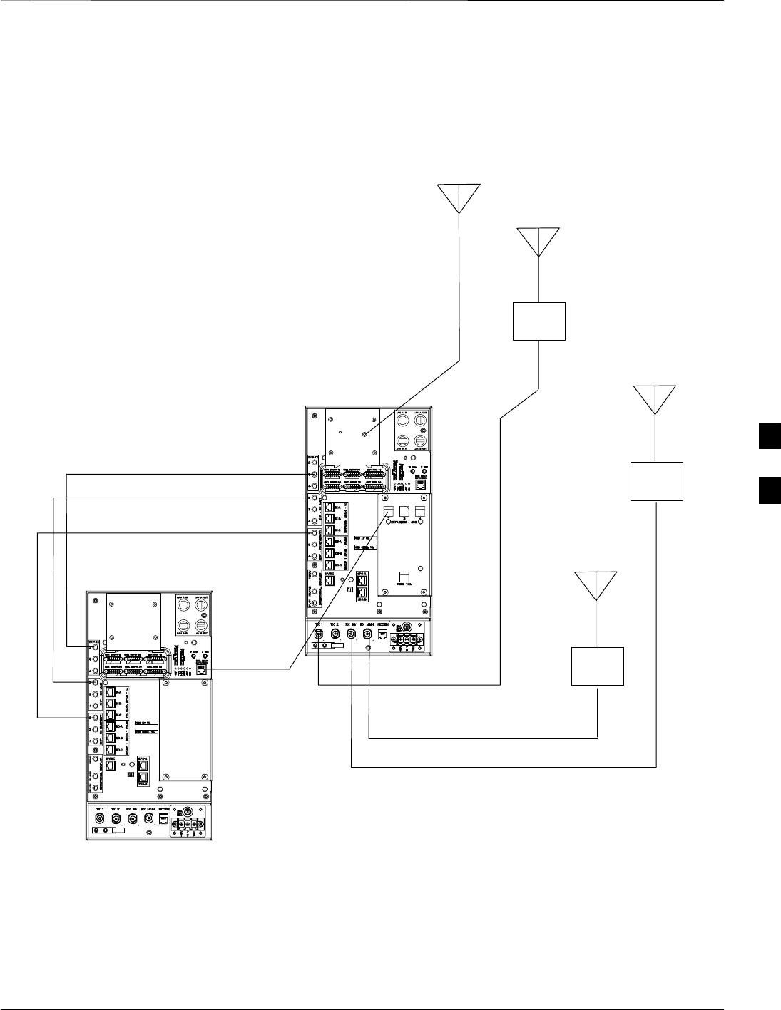
Compact BTS Expansion Configuration (Indoor) – continued
MAY 2004 1X SC480 BTS Hardware Installation, Optimization/ATP, and FRU E-19
PRELIMINARY
EXPANSION 1
STARTER
LOCAL GPS
Figure E-9: One Expansion BTS Cabling Diagram
Power and Ground not shown
Ensure that the expansion
BTS has an expansion cMPC
card installed.
TX 1
RX MAIN
RX DIV
LA
LA
LA
E

Compact BTS Expansion Configuration (Indoor) – continued
E-20 1X SC480 BTS Hardware Installation, Optimization/ATP, and FRU MAY 2004
PRELIMINARY
Table E-11: BBX (Carrier) to cCLPA Via RS485
BTS cCLPA
Starter – BBX1 cCLPA–1
Starter – BBX4 cCLPA–1
Expansion 1 – BBX1 cCLPA–2
Expansion 1 – BBX4 cCLPA–2
Expansion 2 – BBX1 cCLPA–1
Expansion 2 – BBX4 cCLPA–1
Expansion 3 – BBX1 cCLPA–2
Expansion 3 – BBX4 cCLPA–2
Table E-12 shows in tabular format the BTS–to–cCLPA cabling of
Figure E-1.
Table E-12: Starter and Three Expansion BTS Cabling for
Circuit or Packet to Dual cCLPAs
BTS cCLPA
Starter – BBX1 CPA–A (CPA–1)
Starter – BBX4 CPA–A (CPA–1)
Expansion 1 – BBX1 CPA–B (CPB–2)
Expansion 1 – BBX4 CPA–B (CPB–2)
Expansion 2 – BBX1 CPA–A (CPA–1)
Expansion 2 – BBX4 CPA–A (CPA–1)
Expansion 3 – BBX1 CPA–B (CPA–2)
Expansion 3 – BBX4 CPA–B (CPA–2)
Starter and Two Expansion
BTSes to cCLPA Cabling
Table E-13 shows in tabular format the BTS–to–cCLPA cabling of
Figure E-2.
E

Compact BTS Expansion Configuration (Indoor) – continued
MAY 2004 1X SC480 BTS Hardware Installation, Optimization/ATP, and FRU E-21
PRELIMINARY
Table E-13: Starter and Two Expansion BTS Cabling for
Circuit or Packet to Dual cCLPAs
BTS cCLPA
Starter – BBX1 CPA–A (CPA–1)
Starter – BBX4 CPA–A (CPA–1)
Expansion 1 – BBX1 CPA–B (CPB–2)
Expansion 1 – BBX4 CPA–B (CPB–2)
Expansion 2 – BBX1 CPA–A (CPA–1)
Expansion 2 – BBX4 CPA–A (CPA–1)
Starter and One Expansion
BTS to cCLPA Cabling
Table E-14 shows in tabular format the BTS–to–cCLPA cabling of
Figure E-3.
Table E-14: Starter and One Expansion BTS Cabling for
Circuit or Packet to Dual cCLPAs
BTS cCLPA
Starter – BBX1 CPA–A (CPA–1)
Starter – BBX4 CPA–A (CPA–1)
Expansion 1 – BBX1 CPA–B (CPB–2)
Expansion 1 – BBX4 CPA–B (CPB–2)
E

Multiple Compact BTS Configuration (Outdoor)
E-22 1X SC480 BTS Hardware Installation, Optimization/ATP, and FRU MAY 2004
PRELIMINARY
Introduction
This section covers only the outdoor version of the multiple Compact
BTS configuration.
Materials Needed
The following materials are required to configure expansion BTSes.
SVaried length cables with RJ45 connectors
SVaried length cables with RF connectors
SConduit (customer supplied)
SDC Power source (custoemr supplied)
SBattery Backup (customer supplied)
External Combiner and
Directional Coupler
A combiner and directional coupler are required for some of the
configurations. The following are the recommended specifications for
the combiner and directional coupler.
Table E-15: Combiner and Directional Coupler Specifications
Item Specifications
Combiner
Connector: N–Type
Frequency Range: Up to 2 GHz
Insertion Loss: 3.5 dB maximum
Return Loss: 16 dB minimum
Average Input Power: 60 Watts minimum
Directional Coupler
Connector: N–Type
Frequency Range: 810 to 950 MHz
Coupling: 30 +/–1 dB
Directivity: 28 dB minimum
Return Loss: 18 dB minimum
Average Input Power: 10 Watts minimum
SMotorola recommended directional coupler is P/N 809643T03
SRecommended cable with combiner is Andrew LDF4–50 or
equivalent
E

Multiple Compact BTS Configuration (Outdoor) – continued
MAY 2004 1X SC480 BTS Hardware Installation, Optimization/ATP, and FRU E-23
PRELIMINARY
SDirectional coupler and combiner are not environmentally protected ,
and so must be placed within the TME.
ExpansionCompact BTS
Installation Procedure
Follow the procedure in Table E-16for installation of multiple Compact
BTSes.
Table E-16: Procedure for Installing Expansion Compact BTSes
Step Action
1Follow the procedure in Chapter 4 for installing a Compact BTS in a rack.
2For a 3 BTS expansion configuration, follow Figure E-1. Proceed to step 3.
2a For a 2 BTS expansion configuration, follow Figure E-2. Proceed to step 3.
2b For a 1 BTS expansion configuration, follow Figure E-3. Proceed to step 3.
3If conduit is not used, dress cables as necessary.
4Perform Optimization and ATP as described in Chapter 6. LMF Help provides further information.
Frame ID Switch Settings
Refer to Chapter 5, Figure 5-1 or Figure 5-2 or Table 5-1 through
Table 5-4 for the Frame DIP Switch settings.
E
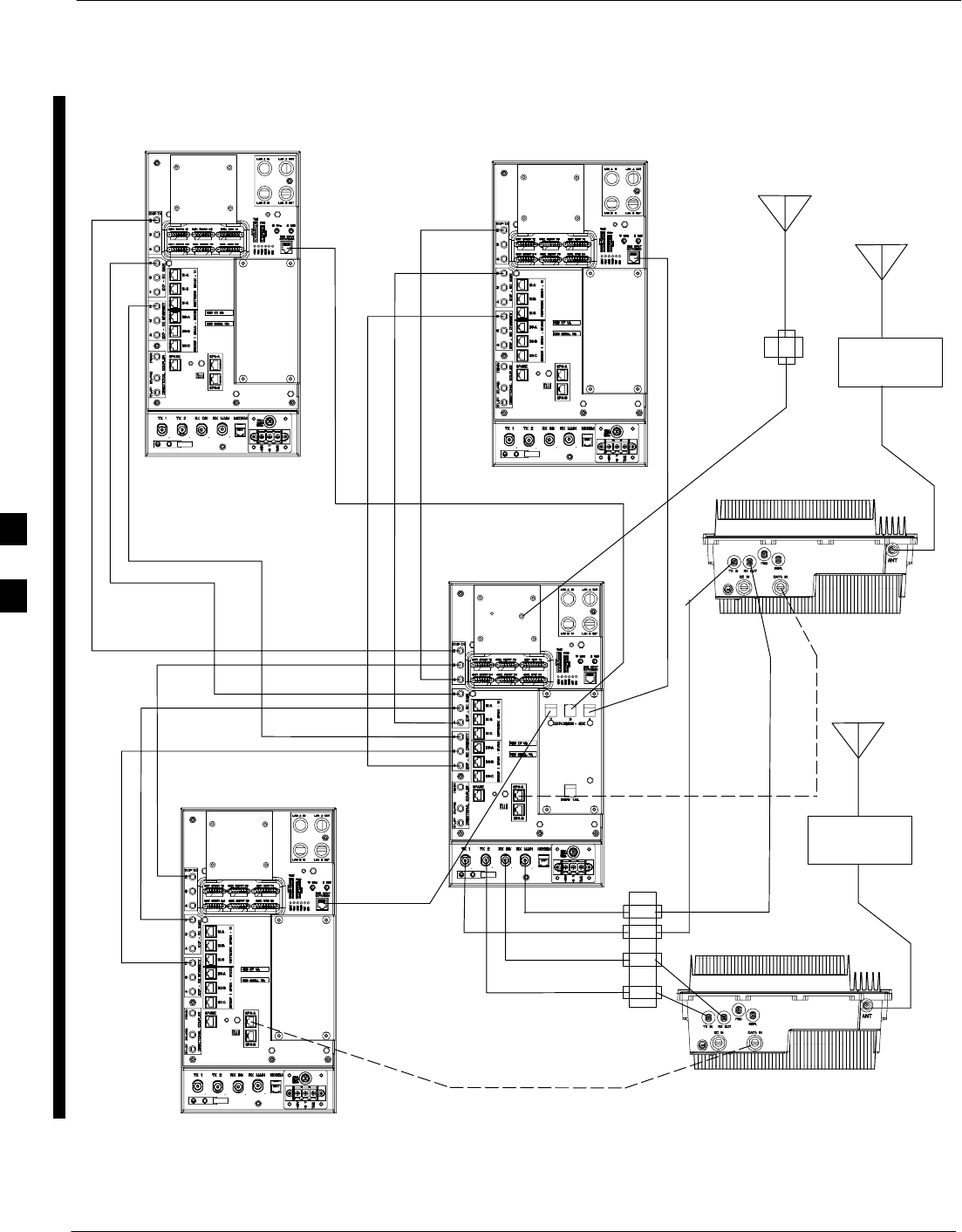
Multiple Compact BTS Configuration (Outdoor) – continued
E-24 1X SC480 BTS Hardware Installation, Optimization/ATP, and FRU MAY 2004
PRELIMINARY
Figure E-10: Three Expansion BTSes Cabling Diagram
LIGHTNING
ARRESTOR
LIGHTNING
ARRESTOR
EXPANSION 3
EXPANSION 2
EXPANSION 1
STARTER
cCLPA 1
cCLPA 2
LOCAL GPS
TX1
TX2
RX DIV
RX MAIN
TME ANTENNA
CONNECTORS
TME
RF–GPS
CONNECTOR
Power and Ground not shown
E
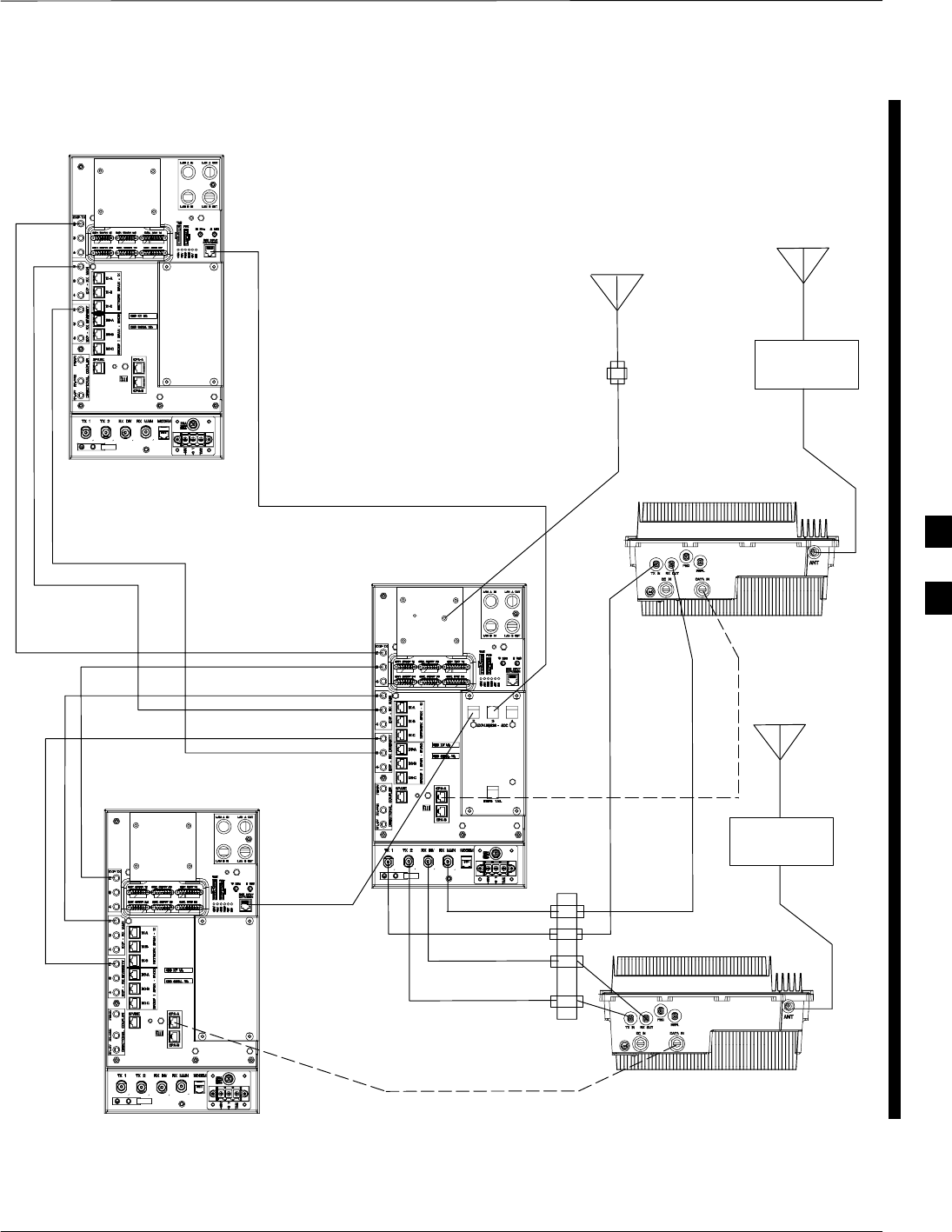
Multiple Compact BTS Configuration (Outdoor) – continued
MAY 2004 1X SC480 BTS Hardware Installation, Optimization/ATP, and FRU E-25
PRELIMINARY
Figure E-11: Outdoor Two Expansion BTSes Cabling Diagram
LIGHTNING
ARRESTOR
LIGHTNING
ARRESTOR
EXPANSION 2
EXPANSION 1
STARTER
cCLPA 1
cCLPA 2
LOCAL GPS
TME
RF–GPS
CONNECTOR
TX2
TX1
RX MAIN
RX DIV
TME ANTENNA
CONNECTORS
Power and Ground not shown
E
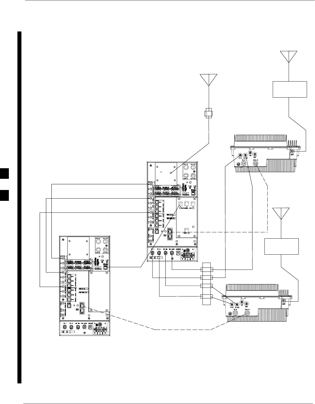
Multiple Compact BTS Configuration (Outdoor) – continued
E-26 1X SC480 BTS Hardware Installation, Optimization/ATP, and FRU MAY 2004
PRELIMINARY
LIGHTNING
ARRESTOR
LIGHTNING
ARRESTOR
EXPANSION 1
STARTER
cCLPA 1
cCLPA 2
LOCAL GPS
Figure E-12: Outdoor One Expansion BTS Cabling Diagram
TME
RF–GPS
CONNECTOR
TX1
RX MAIN
RX DIV
TX2
TME ANTENNA
CONNECTORS
Power and Ground not shown
Other Diagrams
For single cCLPA and no cCLPA, refer to the diagrams for indoor and
allow for the TME connectors as shown in the diagrams presented in this
appendix.
E

MAY 2004 1X SC480 BTS Hardware Installation, Optimization/ATP, and FRU
PRELIMINARY
Appendix F: Logical BTS Configuration
Appendix Content
Logical BTS LAN Configuration for Compact BTS (Indoor) F-1 . . . . . . . . . . . . . .
Introduction F-1 . . . . . . . . . . . . . . . . . . . . . . . . . . . . . . . . . . . . . . . . . . . . . .
Materials Needed F-1 . . . . . . . . . . . . . . . . . . . . . . . . . . . . . . . . . . . . . . . . . .
Frame ID Switch Settings F-1 . . . . . . . . . . . . . . . . . . . . . . . . . . . . . . . . . . .
Logical BTS LAN Cabling Installation Procedure F-3 . . . . . . . . . . . . . . . .
F

Table of Contents – continued
1X SC480 BTS Hardware Installation, Optimization/ATP, and FRU MAY 2004
PRELIMINARY
Notes
F

Logical BTS LAN Configuration for Compact BTS (Indoor)
MAY 2004 1X SC480 BTS Hardware Installation, Optimization/ATP, and FRU F-1
PRELIMINARY
Introduction
This appendix covers only the Logical BTS configuration for cicruit
Compact BTS. The diagrams cover only the LAN connections. This
configuration is set up to be used only with other Compact BTSes.
Power and ground cabling are not shown.
The LAN operates at 10Mbps which is an ethernet standard. It provides
an interface for each GLI in the confiiguration.
Refer to Figure 6-1 for location of the LAN connectors. In circuit mode,
the LAN connections are used by the LMF to download data, and for use
in calibration, acceptance testing, and optimization.
Use these diagrams in conjunction with the diagrams for expansion
BTSes in Appendix E.
Materials Needed
The following materials are required to configure LAN connections
BTSes.
S7 – RG–58 U cables (Length depends on spacing)
S14 – BNC, Terminaton Resistor Plugs (IEC 169–8 spec)
S2 – BNC, 50 Ohm terminations
BTS ID Switch Settings
Refer to Chapter 5, Figure 5-1 or Figure 5-2 or Table 5-1 through
Table 5-4 for the BTS DIP Switch settings.
EXPANSION 3
EXPANSION 2
EXPANSION 1
STARTER
Figure F-1: Three Expansion BTSes LAN Cabling Diagram
Aout Bout
Ain Bin Aout Bout
Ain Bin Aout Bout
Ain Bin Aout Bout
Ain Bin
50–ohm
Load
50–ohm
Load
F
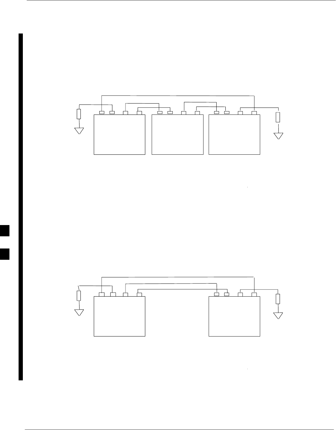
Logical BTS LAN Configuration for Compact BTS (Indoor) – continued
F-2 1X SC480 BTS Hardware Installation, Optimization/ATP, and FRU MAY 2004
PRELIMINARY
EXPANSION 2
EXPANSION 1
STARTER
Figure F-2: Two Expansion BTSes LAN Cabling Diagram
Aout Bout
Ain Bin Aout Bout
Ain Bin Aout Bout
Ain Bin
50–ohm
Load
50–ohm
Load
EXPANSION 1
STARTER
Figure F-3: One Expansion BTSes LAN Cabling Diagram
Aout Bout
Ain Bin Aout Bout
Ain Bin
50–ohm
Load
50–ohm
Load
F

Logical BTS LAN Configuration for Compact BTS (Indoor) – continued
MAY 2004 1X SC480 BTS Hardware Installation, Optimization/ATP, and FRU F-3
PRELIMINARY
Logical BTS LAN Cabling
Installation Procedure
Follow the procedure in Table F-1 for installation of LAN cables for
Logical BTS.
Table F-1: Procedure for Installing LAN Cabling for Logical BTS
Step Action
1Follow the procedure in Chapter 4 for installing a Compact BTS in a rack.
2For a 3 BTS expansion configuration, follow Figure F-1. Proceed to step 3.
2a For a 2 BTS expansion configuration, follow Figure F-2. Proceed to step 3.
2b For a 1 BTS expansion configuration, follow Figure F-3. Proceed to step 3.
3Route LAN cables through conduit from Starter to Expansion BTS 1.
4Route LAN cables through conduit from Starter to Expansion BTS 2 or 3 (depending on
configuration).
5If in use, route LAN cables from Expansion BTS 1 to Expansion BTS 2.
6If in use, route LAN cables from Expansion BTS 2 to Expansion BTS 3.
7Ensure that unused LAN connections are terminated in 50 ohms.
8If not already performed, proceed to Appendix E for expansion cabling diagrams.
9Perform Optimization and ATP as described in Chapter 6. LMF Help provides further information.
F

Logical BTS LAN Configuration for Compact BTS (Indoor) – continued
F-4 1X SC480 BTS Hardware Installation, Optimization/ATP, and FRU MAY 2004
PRELIMINARY
Notes
F

MAY 2004 1X SC480 BTS Hardware Installation, Optimization/ATP, and FRU
PRELIMINARY
Appendix G: Integrated BTS Router Preliminary Operations
Appendix Content
Integrated BTS Router Preliminary Operations – Introduction G-1 . . . . . . . . . . . . .
Introduction G-1 . . . . . . . . . . . . . . . . . . . . . . . . . . . . . . . . . . . . . . . . . . . . . .
Preliminary Operations G-1 . . . . . . . . . . . . . . . . . . . . . . . . . . . . . . . . . . . . .
When to Perform the Verifications G-1 . . . . . . . . . . . . . . . . . . . . . . . . . . . .
Verify GLI3 Software Version and Span Parameter Settings G-2 . . . . . . . . . . . . . . .
Verify GLI3 Software Version and Span Parameter Settings G-2 . . . . . . . .
Required Items G-2 . . . . . . . . . . . . . . . . . . . . . . . . . . . . . . . . . . . . . . . . . . . .
Verifying GLI3 Software Version and Span Parameter Settings G-2 . . . . . .
Change GLI3 Span Parameter Settings G-6 . . . . . . . . . . . . . . . . . . . . . . . . . . . . . . .
Change GLI3 Span Parameter Configuration G-6 . . . . . . . . . . . . . . . . . . . .
G

Table of Contents – continued
1X SC480 BTS Hardware Installation, Optimization/ATP, and FRU MAY 2004
PRELIMINARY
Notes
G

Integrated BTS Router Preliminary Operations – Introduction
MAY 2004 1X SC480 BTS Hardware Installation, Optimization/ATP, and FRU G-1
PRELIMINARY
Introduction
The information and procedures provided are performed in cases where
the GLI3 load and span parameters need to be verified.
Preliminary Operations
Implementing the Integrated BTS Router (IBR) function requires some
preliminary checks of the GLI3 cards which will be used. This appendix
provides the procedures to accomplish these checks. The checks are:
SVerification that IBR–capable software is installed on GLI3 cards
which will be used for IBR
SVerification that span parameter settings on GLI3 cards match the
requirement for the spans at the BTS where the cards will be installed.
When to Perform the
Verifications
All preliminary verifications provided in this chapter can be performed
at either the BTS site or in a central facility equipped to power–up the
GLI3 cards. Depending on the circumstances of the cards’ use, however,
it may be advantageous in reducing the on–site upgrade time and
logistics to perform some of the verifications prior to installation at the
BTS site. Table G-1 lists card conditions of use and the corresponding
suggested verification locations for the software version and span
parameter settings.
Table G-1: Suggested Preliminary Verification Locations
GLI3 Card Condition Installation
Location Software Version
Verification
Location
Span Parameter
Settings Verification
Location
Installed and operating
(circuit or packet) Site where installed At site Not required unless
span type will
change
Different operating
site from where
currently installed
At site where
currently installed Before or after
installation at
different site
G

Verify GLI3 Software Version and Span Parameter Settings
G-2 1X SC480 BTS Hardware Installation, Optimization/ATP, and FRU MAY 2004
PRELIMINARY
Verify GLI3 Software Version
and Span Parameter Settings
Software Version Verification – Before upgrading a BTS to packet
backhaul with an IBR, the software version installed in the GLI3 card or
cards must be verified. If the installed software version does not support
IBR functionality, it must be upgraded to a version which does. For BTS
sites which are already in operation, the upgrade can be done through a
network download to the GLI3 once it is installed. For cards to be
installed in new BTS sites not previously in operation, the upgrade
requires special procedures, and must be done with Motorola Field
Operations or Account Team assistance.
Span Parameter Settings – Prior to initializing a GLI3 card for the first
time in a live circuit BTS or IBR packet BTS site, the span parameter
settings in the card must be verified as matching those provisioned in the
OMC–R database. If the settings are not correct, the card will be unable
to communicate with the RAN network elements and the site will not go
into service. Procedures are included in this section to change the GLI3
card span parameter settings if this is necessary to match those required
for the BTS.
Required Items
The following items are required to perform the verification:
SLocal Maintenance Facility (LMF) computer with the LMF
application program version installed which is compatible with the
software release installed on the BSS refer to Chapter 6
Optimization/ATP in this manual.
SOne of the following
– Motorola cable part number CGDSMMICABLE219112
– Fabricated DB–9 receptacle–to–8–contact MMI connector cable
(see the MMI Cable Fabrication Section of Appendix D for
fabrication instructions and Figure 6-9 for connection)
– SLN2006A MMI Interface Kit (this kit is no longer available to
order), consisting of the following:
–– Motorola Model TRN9666A null modem board
–– Motorola 3009786R01 MMI cable or equivalent
S(For use with SLN2006A only) Straight–through RS–232 cable,
DB–9 to DB–9, and DB–9 to DB–25 connector adapter (see
Figure D-1)
Verifying GLI3 Software
Version and Span Parameter
Settings
Follow the procedure in Table G-2 to verify GLI3 card software version
and span parameter settings.
G

Verify GLI3 Software Version and Span Parameter Settings – continued
MAY 2004 1X SC480 BTS Hardware Installation, Optimization/ATP, and FRU G-3
PRELIMINARY
Table G-2: Verify GLI3 Software Version and Span Parameter Settings
Step Action
1If it has not been done, start a GLI3 MMI communication session on the LMF computer as described
in Table 6-11.
2Verify the installed software version by entering the following at the GLI3 prompt:
display version
3Response to the command will depend on the operating mode of the card. Responses similar to the
following will be displayed for:
3a – Cards in circuit mode:
GLI3> display version
01.09.1980 20:01:59 MGLI–002–2 OOS–SBY BTS–CDMA 16.41.200.14
RAM version: 16.41.200.14
ROM version: 16.41.200.14
Built: Tue Oct 21 09:52:28 2003 il27–2112
Bootrom version: 16.41.200.12
Bootrom Built: Thu Oct 2 03:11:34 2003 IL27–0775
Bootblock version: 16.1.59.00
Bootblock Built: Wed Apr 10 07:08:06 2002 RIPCORD004
This GLI board is in RAM
Booted from /nvram00/loads/gli3_ckt_rom_upgrade.elf
Next boot from /nvram00/loads/gli3_ckt_rom_upgrade.elf
GLI3>
. . . continued on next page G

Verify GLI3 Software Version and Span Parameter Settings – continued
G-4 1X SC480 BTS Hardware Installation, Optimization/ATP, and FRU MAY 2004
PRELIMINARY
Table G-2: Verify GLI3 Software Version and Span Parameter Settings
Step Action
3b – For cards in packet mode:
GLI3> display version
03.23.2004 18:16:07 MGLI–250–1 CC PRESENT BTS–CDMA 16.41.00.11
INTERNAL RAM VERSION: 16.41.0.11
RAM Built: Tue Mar 2 04:59:33 2004 il27–2112
BOOTROM VERSION: 16.41.00.08
BOOTROM Built: Tue Feb 17 10:52:27 2004 il27–0507
BOOTBLOCK VERSION: 16.1.59.00
BOOTBLOCK Built: Wed Apr 10 07:08:06 2002 RIPCORD004
SYSTEM VERSION: 2.16.4.50.15
COMMITTED VERSION: 2.16.4.50.15
NEXT VERSION: 2.16.4.50.15
BACK UP VERSION 2.16.4.50.10
CURRENT RELEASE PATH: /nvram00/screl/2.16.4.50.15/
CURRENT LIF: /nvram00/screl/2.16.4.50.15/NE_LIF.xml
CURRENT IMAGE: /nvram00/screl/2.16.4.50.15/gli_ram.bin.0108
CODE SERVER: 128.0.0.1
GLI3>
4Note the bootROM or System version numbers displayed and determine if the GLI3 is loaded with
IBR–capable code as follows:
SIf the booROM version number is 2.16.41.00.08 or later, the GLI3 is IBR–capable
SIf the System version number is 2.16.4.50.7 or later (for example, 2.16.4.50.25), the GLI3 is
IBR–capable
NOTE
If the card is to be installed in a new BTS site which has not previously been in operation, contact the
local Motorola Account Team for assistance in upgrading the card with IBR–capable software version.
. . . continued on next page
G

Verify GLI3 Software Version and Span Parameter Settings – continued
MAY 2004 1X SC480 BTS Hardware Installation, Optimization/ATP, and FRU G-5
PRELIMINARY
Table G-2: Verify GLI3 Software Version and Span Parameter Settings
Step Action
5Verify the span parameter settings for frame format, equalization, and linkspeed by entering the
following at the GLI3> prompt:
config ni current
The system will respond with a display similar to the following:
The frame format in flash is set to use T1_2.
Equalization:
Span A – Default (0–131 feet for T1/J1, 120 Ohm for E1)
Span B – Default (0–131 feet for T1/J1, 120 Ohm for E1)
Span C – Default (0–131 feet for T1/J1, 120 Ohm for E1)
Span D – Default (0–131 feet for T1/J1, 120 Ohm for E1)
Span E – Default (0–131 feet for T1/J1, 120 Ohm for E1)
Span F – Default (0–131 feet for T1/J1, 120 Ohm for E1)
Linkspeed: Default (56K for T1 D4 AMI, 64K otherwise)
Currently, the link is running at the default rate
The actual rate is 0
NOTE
SDefaults for span equalization are 0–131 feet for T1/J1 spans and 120 Ohm for E1.
SDefault linkspeed is 56K for T1 D4 AMI spans and 64K for all other types.
SThere is no need to change from defaults unless the provisioned span configuration requires it.
6The span parameter settings in the GLI must match those provisioned in the OMC–R database for the
BTS. If they do not, proceed to Table G-3 in the Change GLI3 Span Parameter Settings section.
7If no other MMI actions are required for the card, terminate the MMI communication session and
disconnect the LMF computer from the card.
G

Change GLI3 Span Parameter Settings
G-6 1X SC480 BTS Hardware Installation, Optimization/ATP, and FRU MAY 2004
PRELIMINARY
Change GLI3 Span Parameter
Configuration
If span parameter settings in the GLI3 card do not match the OMC–R
database span parameters for the BTS where they are to be installed,
follow the procedure in Table G-3 to change them.
Table G-3: Set GLI3 Span Parameter Configuration
Step Action
1If it has not been done, start a GLI3 MMI communication session on the LMF computer as described
in Table 6-11.
2At the GLI3> prompt, enter the following:
config ni format
The terminal will display a response similar to the following:
COMMAND SYNTAX: config ni format option
Next available options:
LIST – option : Span Option
E1_1 : E1_1 – E1 HDB3 CRC4 no TS16
E1_2 : E1_2 – E1 HDB3 no CRC4 no TS16
E1_3 : E1_3 – E1 HDB3 CRC4 TS16
E1_4 : E1_4 – E1 HDB3 no CRC4 TS16
T1_1 : T1_1 – D4, AMI, No ZCS
T1_2 : T1_2 – ESF, B8ZS
J1_1 : J1_1 – ESF, B8ZS (Japan) – Default
J1_2 : J1_2 – ESF, B8ZS
T1_3 : T1_3 – D4, AMI, ZCS
>
NOTE
With this command, all active (in–use) spans will be set to the same format.
3To set or change the span type, enter the correct option from the list at the entry prompt (>), as shown
in the following example:
> T1_2
NOTE
The entry is case–sensitive and must be typed exactly as it appears in the list. If the entry is typed
incorrectly, a response similar to the following will be displayed:
CP: Invalid command
01.061980 00:11’59 MGLI–000–2 INS–ACT BTS–CDMA 16.1.68.00
GLI3>
. . . continued on next page
G

Change GLI3 Span Parameter Settings – continued
MAY 2004 1X SC480 BTS Hardware Installation, Optimization/ATP, and FRU G-7
PRELIMINARY
Table G-3: Set GLI3 Span Parameter Configuration
Step Action
4An acknowledgement similar to the following will be displayed:
The value has been programmed. It will take effect after the next reset.
GLI3>
5If the current GLI span rate must be changed, enter the following MMI command:
config ni linkspeed
A response similar to the following will be displayed :
Next available options:
LIST – linkspeed : Span Linkspeed
56K : 56K (default for T1_1 and T1_3 systems)
64K : 64K (default for all other span configurations)
>
NOTE
With this command, all active (in–use) spans will be set to the same linkspeed.
6To set or change the span linkspeed, enter the required option from the list at the entry prompt (>), as
shown in the following example:
> 64K
NOTE
The entry is case–sensitive and must be typed exactly as it appears in the list. If the entry is typed
incorrectly, a response similar to the following will be displayed:
CP: Invalid command
01.061980 00:12’04 MGLI–000–2 INS–ACT BTS–CDMA 16.1.68.00
GLI3>
7An acknowledgement similar to the following will be displayed:
The value has been programmed. It will take effect after the next reset.
GLI3>
. . . continued on next page
G

Change GLI3 Span Parameter Settings – continued
G-8 1X SC480 BTS Hardware Installation, Optimization/ATP, and FRU MAY 2004
PRELIMINARY
Table G-3: Set GLI3 Span Parameter Configuration
Step Action
8If the span equalization must be changed, enter the following MMI command:
config ni equal
A response similar to the following will be displayed:
COMMAND SYNTAX: config ni equal span equal
Next available options:
LIST – span : Span
a : Span A
b : Span B
c : Span C
d : Span D
e : Span E
f : Span F
>
. . . continued on next page
G

Change GLI3 Span Parameter Settings – continued
MAY 2004 1X SC480 BTS Hardware Installation, Optimization/ATP, and FRU G-9
PRELIMINARY
Table G-3: Set GLI3 Span Parameter Configuration
Step Action
9At the entry prompt (>), enter the designator from the list for the span to be changed as shown in the
following example:
> a
A response similar to the following will be displayed :
COMMAND SYNTAX: config ni equal a equal
Next available options:
LIST – equal : Span Equalization
0 : 0–131 feet (default for T1/J1)
1 : 132–262 feet
2 : 263–393 feet
3 : 394–524 feet
4 : 525–655 feet
5 : LONG HAUL
6 : 75 OHM
7 : 120 OHM (default for E1)
8 : T1 Long Haul mode. No Attenuation
9 : T1 Long Haul mode. 7.5 dB Attenuation
10 : T1 Long Haul mode. 15.0 dB Attenuation
11 : T1 Long Haul mode. 22.5 dB Attenuation
12 : E1 Long Haul mode.
>
! CAUTION
When selecting span equalization settings, comply with the following or the BTS may operate
erratically or unpredictably:
SFor ALL BTS types, do not select any of the following settings if they are displayed:
– 5 LONG HAUL
– 6 75 OHM
– 11 T1 Long Haul mode. 22.5 dB Attenuation
– 12 E1 Long Haul mode
SFor four–digit BTSs supported with Channel Service Units (CSU), do not select any of the
following additional settings:
– 8 T1 Long Haul mode. No Attenuation
– 9 T1 Long Haul mode. 7.5 dB Attenuation
– 10 T1 Long Haul mode. 15.0 dB Attenuation
. . . continued on next page
G

Change GLI3 Span Parameter Settings – continued
G-10 1X SC480 BTS Hardware Installation, Optimization/ATP, and FRU MAY 2004
PRELIMINARY
Table G-3: Set GLI3 Span Parameter Configuration
Step Action
10 At the entry prompt (>), enter the code for the required equalization from the list as shown in the
following example:
> 0
A response similar to the following will be displayed :
> 0
The value has been programmed. It will take effect after the next reset.
GLI2>
11 Repeat steps 8 through 10 for each in–use span.
12 NOTE
This step must be performed for GLI3 cards operating on a packet image to ensure the span parameter
changes will replace the previous settings.
For a GLI3 card in packet mode, enter the following:
rmfile /nvram00/config/hlp_param.txt
A response similar to the following will be displayed :
GLI3> rmfile /nvram00/config/hlp_param.txt
11.24.2003 23:14:57 MGLI–004–1 CC PRESENT BTS–CDMA 16.40.00.09
Removing file: /nvram00/config/hlp_param.txt
Successfully removed file: /nvram00/config/hlp_param.txt
GLI3>
13 * IMPORTANT
SAfter executing the config ni format, config ni linkspeed, and/or config ni equal commands,
the affected MGLI/GLI board MUST be reset and reloaded for changes to take effect.
SAlthough defaults are shown in the software, always consult site–specific documentation for span
type, equalization, and linkspeed used at the site where the cards are to be installed.
Reset the card using the MMI reset command.
. . . continued on next page
G

Change GLI3 Span Parameter Settings – continued
MAY 2004 1X SC480 BTS Hardware Installation, Optimization/ATP, and FRU G-11
PRELIMINARY
Table G-3: Set GLI3 Span Parameter Configuration
Step Action
14 Once the card has completed resetting, execute the following command to verify span settings are as
required:
config ni current
A response similar to the following will be displayed :
The frame format in flash is set to use T1_2.
Equalization:
Span A – 0–131 feet
Span B – 0–131 feet
Span C – Default (0–131 feet for T1/J1, 120 Ohm for E1)
Span D – Default (0–131 feet for T1/J1, 120 Ohm for E1)
Span E – Default (0–131 feet for T1/J1, 120 Ohm for E1)
Span F – Default (0–131 feet for T1/J1, 120 Ohm for E1)
Linkspeed: 64K
Currently, the link is running at 64K
The actual rate is 0
15 If the span configuration is not correct, perform the applicable step from this table to change it and
repeat steps 12, 13, and 14 to verify required changes have been programmed.
16 If no other MMI actions are required for the card, terminate the MMI communication session and
disconnect the LMF computer from the card.
G

Change GLI3 Span Parameter Settings – continued
G-12 1X SC480 BTS Hardware Installation, Optimization/ATP, and FRU MAY 2004
PRELIMINARY
Notes
G

MAY 2004 1X SC480 BTS Hardware Installation, Optimization/ATP, and FRU
PRELIMINARY
Appendix H: Integrated BTS Router Installation
Appendix Content
Integrated BTS Router Installation – Introduction H-1 . . . . . . . . . . . . . . . . . . . . . . .
Background H-1 . . . . . . . . . . . . . . . . . . . . . . . . . . . . . . . . . . . . . . . . . . . . . .
New Packet BTS Installation with IBR H-2 . . . . . . . . . . . . . . . . . . . . . . . . . . . . . . .
New Packet BTS Installation H-2 . . . . . . . . . . . . . . . . . . . . . . . . . . . . . . . . .
Prerequisites H-2 . . . . . . . . . . . . . . . . . . . . . . . . . . . . . . . . . . . . . . . . . . . . . .
Implementing IBR Functionality H-2 . . . . . . . . . . . . . . . . . . . . . . . . . . . . . .
BTS Span Connections for IBR H-4 . . . . . . . . . . . . . . . . . . . . . . . . . . . . . . . . . . . . .
BTS Span Connections H-4 . . . . . . . . . . . . . . . . . . . . . . . . . . . . . . . . . . . . .
BTS Span Cable H-4 . . . . . . . . . . . . . . . . . . . . . . . . . . . . . . . . . . . . . . . . . . .
BTS Span Connections for IBR – One Span H-5 . . . . . . . . . . . . . . . . . . . . . . . . . . .
One Span Frame H-5 . . . . . . . . . . . . . . . . . . . . . . . . . . . . . . . . . . . . . . . . . .
H

Table of Contents – continued
1X SC480 BTS Hardware Installation, Optimization/ATP, and FRU MAY 2004
PRELIMINARY
Notes
H

Integrated BTS Router Installation – Introduction
MAY 2004 1X SC480 BTS Hardware Installation, Optimization/ATP, and FRU H-1
PRELIMINARY
Background
The IBR capability was developed to provide a low–cost solution for
providing CDMA packet backhaul benefits at cell sites with lower traffic
volumes. The IBR function is implemented by using the GLI3 card
Concentration Highway Interface (CHI) bus 2 processor to perform the
router function. This is accomplished through changes in the GLI3 card
software. A card with the IBR–capable software can perform as a circuit
GLI3 card, as a GLI3 with IBR, and as a GLI3 used with external BTS
router groups. The card has the capability to recognize the environment
in which it is installed and autoselect the appropriate operating mode
(circuit, IBR packet, external BTS router packet).
Span line channel capability for an IBR–equipped SC480 BTS is limited
to those available on a single T1 or E1 span.
H

New Packet BTS Installation with IBR
H-2 1X SC480 BTS Hardware Installation, Optimization/ATP, and FRU MAY 2004
PRELIMINARY
New Packet BTS Installation
This section covers the actions necessary for implementing IBR packet
capability in the installation of a new BTS. Procedures unique to this
implementation are contained in this section. When procedures required
in this implementation are contained in other parts of this publication or
in other publications, the user will be specifically directed to them at the
appropriate places in this section.
Prerequisites
The following must be accomplished prior to traveling to the BTS site
for IBR implementation:
SThe BTS has been installed as described in Chapter 4 of this manual.
SOne of the following:
– GLI3 card(s) for the site have been verified as having IBR–capable
software image installed
– Motorola Field Operations or Account Team member is identified
to travel to the BTS site to perform GLI3 IBR–capable software
installation, if required
SGLI3 card(s) for the BTS are on hand for transport to the BTS site or
are verified to be at the BTS site
SRequired publications to support IBR implementation activities are on
hand for transportation to the BTS site
Implementing IBR Functionality
Follow the procedure in Table H-1 to implement IBR functionality for
the BTS.
Table H-1: Implement IBR Functionality in New BTS
Step Action
1Upon arrival at the site, contact the OMC–R and notify the operator that site operations are starting.
2If the BTS has not been initially powered up, apply power to the BTS in accordance with the Power
Pre–Power–up Tests and Initial Power–up Tests and Procedures described in Chapter 5 of this manual.
3Once the BTS is fully powered up with these procedures, the GLI3 card should have been seated in the
correct slot. If it is not, seat the card at this time and allow each to complete its initialization.
4If it was not previously done, follow the procedure in Table G-2 to:
SVerify the software version in the GLI3 card(s)
SVerify the span parameter settings in each GLI3 card match those established for the site in the
OMC–R database
5If the GLI3software requires upgrading for IBR capability, request Motorola Field Operations or
Account Team assistance in upgrading the software.
6If GLI3 card span parameter settings do not match those required, change them as necessary by
following the procedure in Table G-3.
. . . continued on next page
H

New Packet BTS Installation with IBR – continued
MAY 2004 1X SC480 BTS Hardware Installation, Optimization/ATP, and FRU H-3
PRELIMINARY
Table H-1: Implement IBR Functionality in New BTS
Step Action
7Refer to the site documentation for IBR spans and inspect the BTS span cabling connections to be sure
they match Figure H-1.
8Correct any cabling discrepancies between the BTS span cabling and site documentation, referring to
Figure H-1 and the Install Span and Alarm Cables and Span Line Cable Pin Numbering Chapter 4 of
this manual as required.
9If the BTS requires optimization and/or ATP, perform them at this time by following the applicable
procedures in Chapter 6 of this manual.
10 When all preparations for BTS operation are completed, contact the OMC–R and notify the operator
that the BTS is ready for operation and request notification when the operator no longer requires
support on–site.
11 When advised that there is no further requirement for on–site support of BTS and IBR initialization,
proceed to Chapter 8 and follow the procedures to prepare to leave the site.
H

BTS Span Connections for IBR
H-4 1X SC480 BTS Hardware Installation, Optimization/ATP, and FRU MAY 2004
PRELIMINARY
BTS Span Connections
The illustration in this section provides the detail of span connection for
a non–redundant BTS to support IBR packet operation. The required
configuration for IBR in redundant BTS is a single span.
BTS Span Cable
All connections in the BTS span connection diagram for IBR are based
on the use of the following Motorola–standard BTS span cable:
Table H-2: BTS Span Cables
Item Part Number Qty Description
BTS span cable CGDS1583461
or
CGDS1583462
1Cable, 50–wire, shielded twisted 25 pair, 100
ohm, 24–AWG, 7.6 m (25 ft – CGDS1583461) or
15.2 m (50 ft – CGDS1583462), one male
50–contact TELCO connector attached. One end
of cable is un–terminated to allow connection to
site termination equipment.
H
BTS Span Connections for IBR – One Span
MAY 2004 1X SC480 BTS Hardware Installation, Optimization/ATP, and FRU H-5
PRELIMINARY
One Span Frame
Figure H-1 illustrates the connection details for one span to support
packet operation with IBR for non–redundant BTS.
Figure H-1: Cabling Compact BTS Packet Operation Integrated BTS Router Spans –
One Span
BTS Termination
Equipment
ALL CROSS–CONNECTS
ARE DONE WITHIN
TERMINATION
EQUIPMENT
SC4812TL0201
PIN 2 RX TIP A
PIN 1 RX RING A
PIN 5 TX TIP A
PIN 4 TX RING A
SPAN I/O A
BTS SPAN
CABLE
ORG–WHT TX TIP
WHT–ORG TX RING
BLU–WHT RX TIP
WHT–BLU RX RING
H

BTS Span Connections for IBR – One Span – continued
H-6 1X SC480 BTS Hardware Installation, Optimization/ATP, and FRU MAY 2004
PRELIMINARY
Notes
H

MAY 2004 1X SC480 BTS Hardware Installation, Optimization/ATP, and FRU
PRELIMINARY
Appendix I: Packet Backhaul Configuration
Appendix Content
Packet Backhaul BTS I-1 . . . . . . . . . . . . . . . . . . . . . . . . . . . . . . . . . . . . . . . . . . . .
Introduction I-1 . . . . . . . . . . . . . . . . . . . . . . . . . . . . . . . . . . . . . . . . . . . . . .
Packet Backhaul BTS Procedures I-1 . . . . . . . . . . . . . . . . . . . . . . . . . . . . .
I

Table of Contents – continued
1X SC480 BTS Hardware Installation, Optimization/ATP, and FRU MAY 2004
PRELIMINARY
Notes
I

Packet Backhaul BTS
MAY 2004 1X SC480 BTS Hardware Installation, Optimization/ATP, and FRU I-1
PRELIMINARY
Introduction
For Packet Backhaul, the LMF Help should be accessed for the
appropriate procedures.
Packet Backhaul BTS
Procedures
Optimization Procedures
SClick on LMF Help
SSelect Optimization/ATP Process
SSelect Optimization procedure for SC48X
– Important CDF Parameters
– CSA
– Optimization of SC48X High Power Configuration
– Optimization of SC48X Low Power Configuration
– Optimization of SC48X High Power in Logical Configuration
– Optimization of SC48X Low Power in Logical Configuration
– Calibrating Procedures for SC48X Expansion Frame Configurations
Follow the appropriate procedure identified in the LMF Help.
I

Packet Backhaul BTS – continued
I-2 1X SC480 BTS Hardware Installation, Optimization/ATP, and FRU MAY 2004
PRELIMINARY
Notes
I

MAY 2004 1X SC480 BTS Hardware Installation, Optimization/ATP, and FRU Index-1
PRELIMINARY
Index
Numbers
10BaseT/10Base2 converter, LMF to BTS
connection, 6-17
A
Abbreviated
RX acceptance test, all–inclusive, 7-5
TX acceptance test, all–inclusive, 7-5
Acceptance Test Procedure. See ATP
Accessing OMCR CLI Window, 10-2
Advantest R3267 Spectrum Analyzer GPIB Address,
B-7
Advantest R3465 Communications Test Set GPIB
Address, B-12
Advantest R3562 Signal Generator GPIB Address,
B-9
Agilent 8935 Series E6380 (formerly HP 8935) Test
Set GPIB Address, B-9
Agilent E4406A, calibration, B-28
Agilent E4406A Transmitter Tester GPIB Address,
B-5
Agilent E4432B Signal Generator GPIB Address, B-6
All Cal/Audit procedure, 6-82
All RX ATP Test Procedure, 7-8
All TX ATP Test Procedure, 7-7
All TX/RX ATP Test Procedure, 7-6
ATP
all inclusive TX acceptance test outline, 7-5
automated introduction, 7-1
code domain noise floor acceptance test procedure,
7-19
code domain power acceptance test procedure, 7-19
failure report generation, 7-23
FER test, frame error rate testing, 7-21
pilot time offset, 7-16
prerequisites, 7-2
spectral purity TX mask, 7-11
test set–up, 6-61
Advantest R3267/R3562, DRDCs, 6-64
Advantest R3465, 6-61
Agilent 8935, DRDCs, 6-61
Agilent 8935/E4432B, DRDCs, 6-63
Agilent E4406A/E4432B, DRDCs, 6-63
CyberTest, 6-61
HP 8921A, 1.9 GHz, 6-62
HP 8921A, 800 MHz, 6-59 , 6-62
waveform quality (Rho), 7-14
waveform quality (RHO) acceptance test procedure,
7-14
ATP – Reduced, 7-1
Attenuator, required test equipment, 1-18
B
Basic Troubleshooting Overview, 11-1
Bay Level Offset calibration
description, 6-76
purpose, 6-76
when to calibrate, 6-76
BBX
carrier spectral purity, 7-11
primary and redundant, TX tests to be performed,
7-9
BLO. See Bay Level Offset calibration
Broad Band Receiver. See BBX
BTS
download, 6-36
Ethernet LAN interconnect diagram, 6-33
LMF connection, 6-16 , 6-17

Index – continued
Index-2 1X SC480 BTS Hardware Installation, Optimization/ATP, and FRU MAY 2004
PRELIMINARY
RX sensitivity/frame error rate, 7-10
system software download, 6-6
BTS Frame Erasure Rate. See FER
BTS Log In Procedure, GUI, 6-25
BTS login
CLI environment, 6-27
General, 6-25
GUI environment, 6-25
BTS Logout
CLI environment, 6-29
GUI environment, 6-28
Create CAL File, 6-88
C
cable calibration, automatic, test set–up, 6-56
Advantest R3267/R3562, 6-57
Advantest R3465, 6-56
Agilent 8935, 6-56
Agilent E4406A/E4432B, 6-57
CyberTest, 6-56
HP 8921A, 6-56
CAL file. See calibration data file
Calibrate Test Cabling Using Signal Generator &
Spectrum Analyzer, 6-71
Calibrating, Test Equipment, 6-68
Calibrating Cables, Overview, 6-69
Calibrating Test Cable Setup, PCS Interface
HP83236B, B-32
Calibrating Test Cabling using Communications
System Analyzer, 6-70
Calibration, required test equipment, 1-14
calibration
calibration data file, 6-77
Gigatronics 8542B, B-31
calibration data file, description of, 6-77
Cannot communicate to Power Meter, 11-5
CCP shelf illustration, left side, 1-24
CDF, 6-5
site equipage verification, 6-6
site type and equipage data information, 6-1
CDMA, subscriber mobile radiotelephone, optional
test equipment, 1-19
Cell Site
equipage verification, 6-2
types configuration, 6-5
Cell Site Data File. See CDF
CLI, 6-24
Clock Sync Module. See CSM
Code domain power/noise floor
acceptance test, 7-18
analyzer display, 7-20
Command Line Interface, 6-24
Communication test set, rear panel, B-18 , B-20
communications test set, TX acceptance tests, 7-4
Connect BTS E1/T1 spans, 8-4
Connect BTS T1/E1 spans, 8-4
Connecting test equipment to the BTS, 6-51
Control, TX output verification, 7-4
Copy and Load Cal File to to CBSC, 8-1
Copy BTS CDF (or NECF) and CBSC CDF Files to
the LMF, 6-12
Copying CAL files from CDMA LMF to the CBSC,
8-1
Copying CAL files to the CBSC, 8-2
CSM
clock source, select, 6-40
enable, 6-41
LEDs, 6-43
system description, 6-43
CSM clock source, select, 6-40
CSM frequency verification, 6-45
D
Devices, download. See Download
Digital multimeter, required test equipment, 1-19
Download
See also Devices
BTS, 6-36
BTS system software, 6-6
Download BLO Procedure, 6-84
download ROM and RAM code. See ROM code
Download/Enable MCCs, 6-42
Download/Enable MGLIs, 6-39

Index – continued
MAY 2004 1X SC480 BTS Hardware Installation, Optimization/ATP, and FRU Index-3
PRELIMINARY
E
E1, isolate BTS from the E1 spans, 6-16
E4406A, calibration, B-28
Enable CSMs. See CSM
Equipment, warm–up, required test equipment, 1-14
Equipment warm-up, 6-55
establish MMI communication, 6-30
Ethernet LAN, interconnect diagram, 6-33
Ethernet LAN termination, 6-3
External Test Equipment Removal, 8-3
F
Failure report generation, 7-23
FER, acceptance test, 7-21
Files, intermediate file, 7-23
files, calibration data, 6-77
Fluke, model 8062A with Y8134 test lead kit, test
equipment, 1-19
Folder Structure Overview, 6-9
Frame, equipage preliminary operations, 6-1
Frequency counter, optional test equipment, 1-19
G
General Purpose Interface Bus, IEEE–488 protocol
interface bus. See GPIB
Generating an ATP Report, 7-23
Gigatronics 8541C Power Meter GPIB Address, B-15
Gigatronics 8542 power meter, calibration, B-31
GPIB, B-17 , B-21 , B-22
cables required test equipment, 1-17
set address, HP 437B, B-14
GPIB Address
Advantest R3267, B-7
Advantest R3465, B-12
Advantest R3562, B-9
Agilent (formerly HP) 8935, B-9
Agilent E4406A, B-5
Agilent E4432B, B-6
Gigatronics 8541C Power Meter, B-15
Hewlett Packard HP8921a & HP83236A/B, B-11
Motorola CyberTest, B-13
GPIB Interface Box, RS232, B-16
GPS Initialization/Verification
estimated position accuracy, 6-46
surveyed position accuracy, 6-46
GPS satellite system, 6-41
GUI, 6-19
H
Hardware Requirements, 1-15
Hewlett Packard, 10833A or equivalent, required test
equipment, 1-17
Hewlett Packard HP8921A and HP83236A/B GPIB
Address, B-11
High–impedance conductive wrist strap, required test
equipment, 1-18
HP 437
Pre–calibration, B-29
setting GPIB address, B-14
HP 83236A, B-21
HP 8921A PCS interface, Cables Connection for 10
MHz Signal and GPIB , B-18 , B-20
HP 8921A/600 test set, 1-16
HP8921A, B-21
Test equipment connections , B-17
HyperTerminal, Creating named HyperTerminal
connection, 6-14
HyperTerminal , create named connection, 6-14
I
IEEE–488 protocol interface bus. See GPIB
Initial HP8921A setup, B-32
Initial Installation of Boards/Modules, preliminary
operations, 6-2
Intermediate file, generate ATP file using, 7-23
L
LAN, tester optional test equipment, 1-19
LAN termination, 6-3
LED, CSM, 6-43
LIF, Load Information File, 6-10
LMF, B-17 , B-22
1X FER acceptance test, 7-4

Index – continued
Index-4 1X SC480 BTS Hardware Installation, Optimization/ATP, and FRU MAY 2004
PRELIMINARY
1X upgrade preparation, home directory, 6-9
BTS connection, 6-17
to BTS connection, 6-16
TX acceptance tests, 7-4
view CDF information, 6-6
LMF BTS displays, 6-19
LMF Removal, 8-4
Load Information File, 6-10
Logging Into a BTS, 6-25
Logging Out, 6-28
M
Motorola CyberTest GPIB Address, B-13
Multi Channel Card. See MCC
N
National Instruments, GPIB–232–CT or equivalent,
required test equipment, 1-16
NECF, 6-5
O
OMCR CLI access procedure, 10-2
Online Help, 6-32
Optional, test equipment list, 1-19
Optional test equipment
CDMA subscriber mobile or portable
radiotelephone, 1-19
frequency counter, 1-19
LAN tester, 1-19
oscilloscope, 1-19
RF test cable, 1-19
spectrum analyzer, 1-19
Oscilloscope, optional test equipment, 1-19
P
PCMCIA, Ethernet adapter, LMF to BTS connection,
6-17
Pilot time offset, acceptance test, 7-16
Ping, 6-33
Policy, required test equipment, 1-14
Power Meter, setting GPIB address, HP437B, B-14
Power meter
required test equipment, 1-17 , 1-18
TX acceptance tests, 7-4
Pre–calibration, HP 437, B-29
Preliminary operations, cell Site types, 6-1
Prepare to leave site
connect BTS E1/T1 spans, 8-4
connect BTS T1/E1 spans, 8-4
Prepare to Leave the Site
External Test Equipment Removal, 8-3
Final Checks before leaving site, 8-5
LMF Removal, 8-4
Re–connect BTS T1 spans, 8-4
Prerequisites, automated acceptance tests, 7-2
Procedures to Copy CAL Files From Diskette to the
CBSC, 8-2
Procedures to Copy Files to a Diskette, 8-1
R
RAM code, described, 6-36
Re–connect BTS T1 Spans, 8-4
receive path, calibration, 6-76
component verification, 6-76
Reduced ATP, 7-1
Report generation, ATP report, 7-23
Required test equipment
calibration, 1-14
communications system analyzer, 1-16
digital multimeter, 1-19
equipment warm–up, 1-14
GPIB cables, 1-17
high–impedance conductive wrist strap, 1-18
list, 1-15
optional equipment, 1-19
policy, 1-14
power meter, 1-17 , 1-18
RF adaptors, 1-18
RF attenuator, 1-18
RF load, 1-18
RS232 to GPIB interface, 1-16
test cable calibration, 1-14
Restore Carrier Signaling Operations for a Circuit
BTS, 10-29
Restore Carrier Signaling Operations for a Packet
BTS, 10-59

Index – continued
MAY 2004 1X SC480 BTS Hardware Installation, Optimization/ATP, and FRU Index-5
PRELIMINARY
Restore Carrier Signaling Operations Procedure For a
Circuit BTS, Starting Up, 10-29
Restore Carrier Signaling Operations Procedure For a
Packet BTS, Starting Up, 10-59
Restore Sector Signaling Operations for a Circuit
BTS, 10-26
Restore Sector Signaling Operations for a Packet
BTS, 10-56
Restore Sector Signaling Operations Procedure For a
Circuit BTS, Starting Up, 10-26
Restore Sector Signaling Operations Procedure For a
Packet BTS, Starting Up, 10-56
Restore Site Signaling Operations for a Circuit BTS,
10-23
Restore Site Signaling Operations Procedure For a
Circuit BTS, Starting Up, 10-23
Restore Site Signaling Operations for a Packet BTS,
10-53
Restore Site Signaling Operations Procedure For a
Packet BTS, Starting Up, 10-53
RF
attenuator, 1-18
load for required test equipment, 1-18
required test equipment load, 1-18
test cable, 1-18
RF path calibration. See Bay Level Offset calibration
Rho
TX waveform quality acceptance test, 7-14
waveform quality requirements, 7-14
ROM code
described, 6-36
downloading, C-1
procedure, C-2
RS232 GPIB Interface Box, B-16
RS232 to GPIB interface, required test equipment,
1-16
RX
acceptance tests, FER, 7-21
sensitivity/frame error rate, 7-10
S
Selecting Test Equipment, 6-66
Set–up for TX Calibration, 6-81
Setting Cable Loss Values, 6-73
Setting TX Coupler Loss Value, 6-74
Shut Down Carrier Signaling Functions for a Circuit
BTS, 10-16
Shut Down Carrier Signaling Functions for a Packet
BTS, 10-46
Shut Down Carrier Signaling Functions Procedure
For a Circuit BTS, Shutting Down, 10-16
Shut Down Carrier Signaling Functions Procedure
For a Packet BTS, Shutting Down, 10-47
Shut Down Sector Signaling Functions for a Packet
BTS, 10-39
Shut Down Sector Signaling Functions for a Circuit
BTS, 10-9
Shut Down Sector Signaling Functions Procedure For
a Circuit BTS, Shutting Down, 10-9
Shut Down Sector Signaling Functions Procedure For
a Packet BTS, Shutting Down, 10-40
Shut Down Site Signaling Functions for a Circuit
BTS, 10-3
Shut Down Site Signaling Functions for a Packet
BTS, 10-32
Shut Down Site Signaling Functions Procedure For a
Circuit BTS, Shutting Down, 10-3
Shut Down Site Signaling Functions Procedure For a
Packet BTS, Shutting Down, 10-33
signal generator, 1X FER acceptance test, 7-4
Site, equipage verification, 6-6
Site equipage, CDF/NECF, 6-5
Software Release caveats, 8-1
Span line, J1 verification equipment, optional test
equipment, 1-19
Spectral purity, TX mask – primary and redundant
BBX, 7-9
Spectral purity transmit mask, acceptance test, 7-11
Spectrum analyzer, optional test equipment, 1-19
Supported Test Sets, 6-51
System Connectivity Test, B-21
T
T1, isolate BTS from the T1 spans, 6-16
Tektronics, model 2445 or equivalent, optional test
equipment, 1-19

Index – continued
Index-6 1X SC480 BTS Hardware Installation, Optimization/ATP, and FRU MAY 2004
PRELIMINARY
Test cable calibration, required test equipment, 1-14
Test Equipment, Calibrating, 6-68
Test equipment
set up, TX output verification/control, 7-4
system analyzer, 1-16
TX acceptance tests, 7-4
Test equipment connections , preliminary Agilent
E4406A/E4432B set–up, B-26
Test Equipment Setup Calibration for TX Bay Level
Offset, B-36
Test Equipment Setup Chart, 6-53
Test equipment setup RF path calibration, 6-78
transmit path, calibration, 6-76
component verification, 6-76
Transmit TX path audit, 6-85
Transmit TX path calibration, 6-79
TX
acceptance tests
code domain power/noise floor, 7-18
equipment setup, 7-4
pilot time offset, 7-16
spectral purity mask, 7-11
spectrum analyzer display, 7-13
waveform quality (rho), 7-14
all inclusive TX ATP test, 7-5
output acceptance tests
code domain power noise, 7-9
pilot time offset, 7-9
waveform quality, 7-9
TX Audit Test, 6-85
Tx BLO Nominal Offset, Setup for TX Cal, 6-82
TX calibration, 6-82
All Cal/Audit, 6-82
set–up, 6-58
Advantest R3267, 6-60
Agilent 8935, 6-58
Agilent E4406A, 6-60
CyberTest, 6-58
TX path calibration, 6-82
U
Updating Calibration Data Files
Copy and Load Cal File to to CBSC, 8-1
Software Release caveats, 8-1
UTP, LMF to BTS connection, 6-17
V
verification during calibration, 6-76
Verify, TX output, 7-4
Verify GLI ROM code load, 6-38
W
Waveform quality (Rho), acceptance test procedure,
7-14
X
Xircom Model PE3–10B2, LMF to BTS connection,
6-17
*68P09260A11−7*
68P09260A11–7

PRELIMINARY
68P09260A11–7
MAY 2004
ENGLISH
CDMA2000 1X
SOFTWARE RELEASE 2.16.4.X
Technical
Information
1X SC480 BTS HARDWARE
INSTALLATION, OPTIMIZATION/ATP, AND
FRU
800 MHZ
SOFTWARE RELEASE 2.16.4.X
800 MHZ
CDMA2000 1X
1X SC480 BTS HARDWARE INSTALLATION, OPTIMIZATION/ATP, AND FRU
ENGLISH
MAY 2004
68P09260A11–7
PRELIMINARY
Technical Information Products and Services
11
STANDARD MANUAL PRINTING INSTRUCTIONS
STANDARD SPECIFICATIONS – FOR REFERENCE–DO NOT MODIFY
Part Number: 68P09260A11–7 APC:
Title: 1X SC480 BTS Hardware Installation, Optimization/ATP, and FRU
379
PAPER:
Body: 70 lb.
Inside Cover: 65 lb. Cougar
Tabs: 110 lb. Index
Binder Cover: Standard TED
cover – 10 pt. Carolina
1st. LEVEL TABS:
Single Sided
5 Cuts
Clear Mylar
Pantone 2706–C
Black Ink
2nd. LEVEL TABS: FINISHING:
3–Ring Binder
Slant–D
3–Hole Punched
(5/16–in. dia.)
Shrink Wrap Body
Black ink for body, inside cover, and binder cover.
SPECIAL INSTRUCTIONS
TAB and SHEET SIZE/QUANTITY
7X9 8.5x11 648 11x17
NON–STANDARD SPECIFICATIONS
Tape Bound Corner Stitch
Other: Meet with manager to determine the deliverable.
Sheets = (Total Pages) / 2
Single Sided
7 Cuts
Clear Mylar
White
Black Ink
Filename: 260A11–7
1st Level Tabs 2nd Level Tabs
Volume MAY 2004of DatePrint Vendor: eDOC