Nokia Solutions and Networks T6BN1 CDMA Base Station User Manual IHET6BN1 Part 1 of 3

Nokia Solutions and Networks CDMA Base Station IHET6BN1 Part 1 of 3

IHET6BN1 User Manual Part 1 of 3
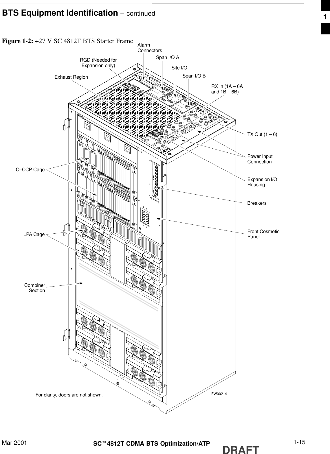
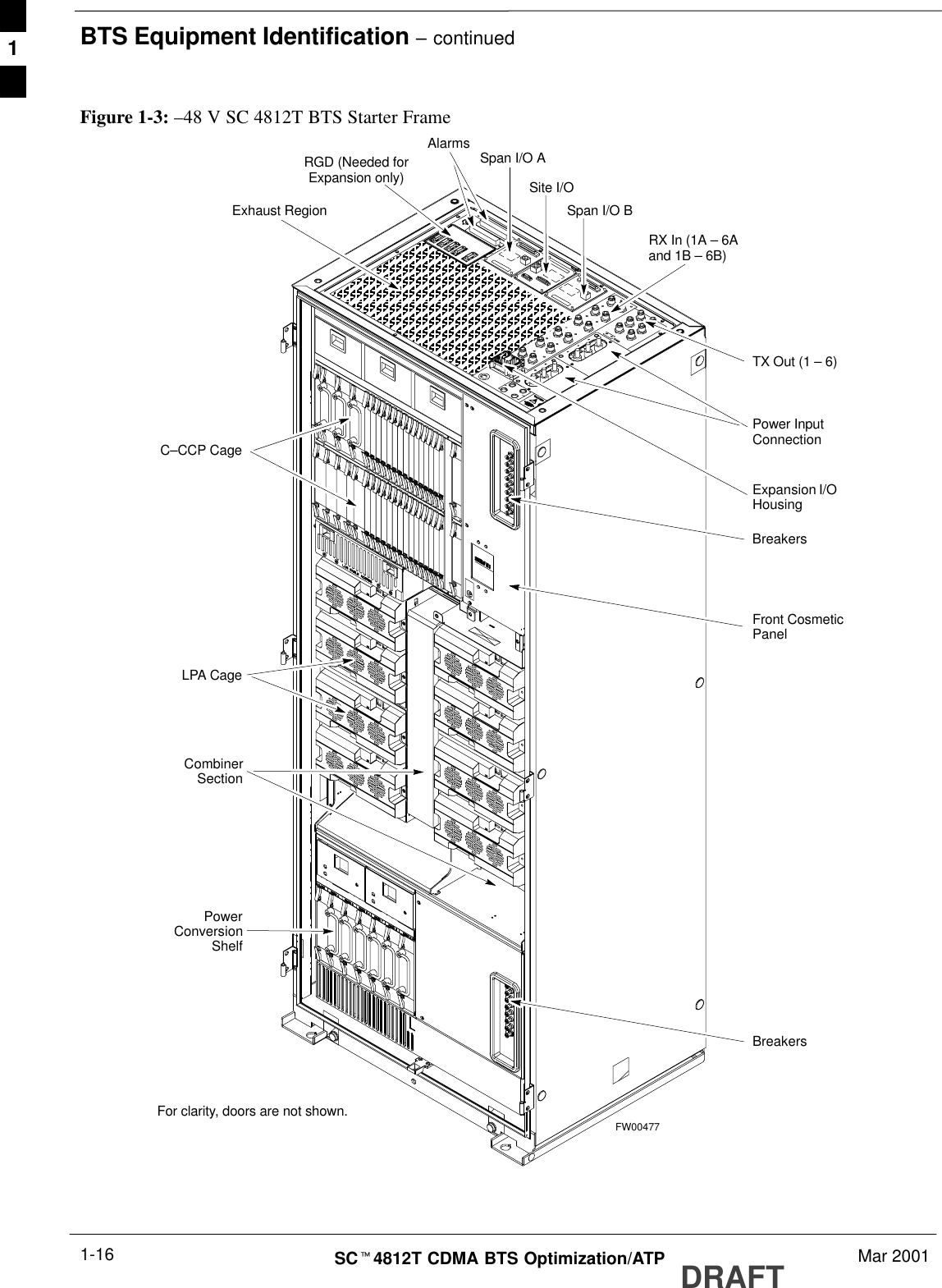
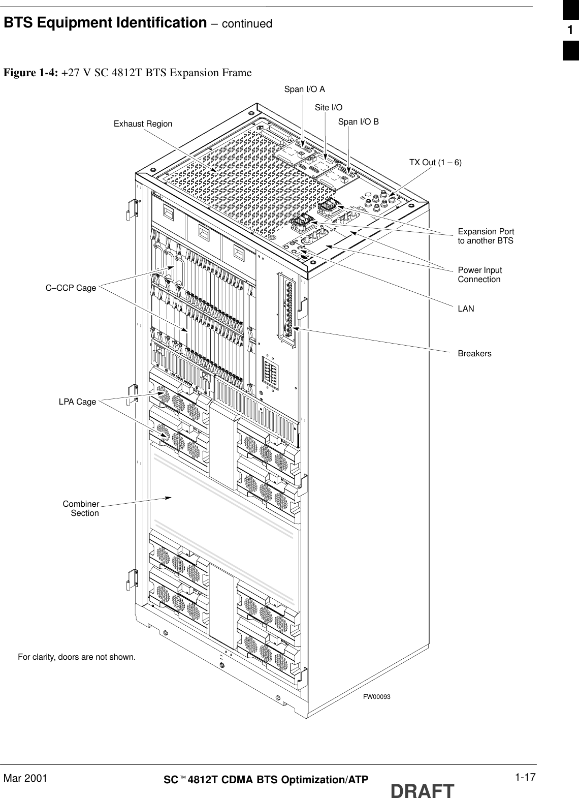
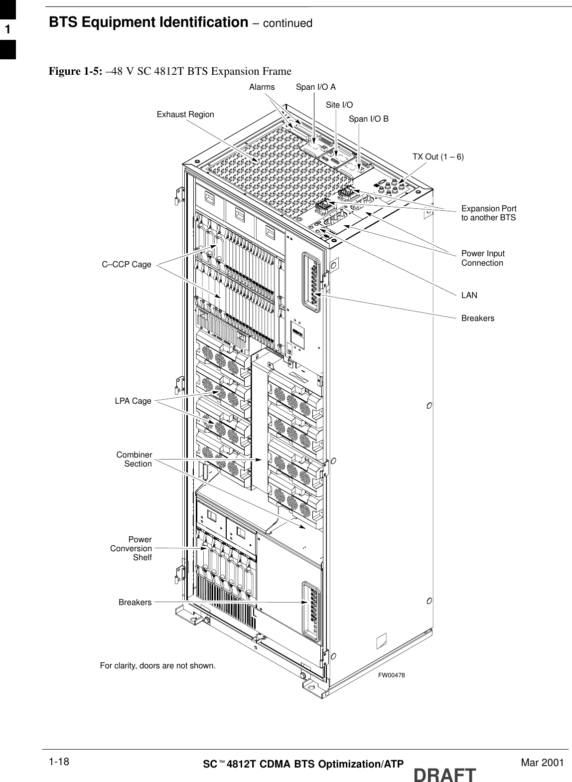
SCt4812T BTS Optimization/ATPSystem Software Release 2.16.0800/1700/1900 MHzCDMAEnglishMar 200168P09253A61–1 DRAFT
EnglishMar 200168P09253A61–1SCt4812T BTS Optimization/ATP800/1700/1900 MHzCDMA
SCt4812T BTS Optimization/ATPSystem Software Release 2.16.0800/1700/1900 MHzCDMAEnglishMar 200168P09253A61–1DRAFT
NoticeWhile reasonable efforts have been made to assure the accuracy of this document, Motorola, Inc. assumes no liability resulting from anyinaccuracies or omissions in this document, or from use of the information obtained herein. The information in this document has beencarefully checked and is believed to be entirely reliable. However, no responsibility is assumed for inaccuracies or omissions. Motorola,Inc. reserves the right to make changes to any products described herein and reserves the right to revise this document and to makechanges from time to time in content hereof with no obligation to notify any person of revisions or changes. Motorola, Inc. does notassume any liability arising out of the application or use of any product, software, or circuit described herein; neither does it conveylicense under its patent rights or the rights of others.It is possible that this publication may contain references to, or information about Motorola products (machines and programs),programming, or services that are not announced in your country. Such references or information must not be construed to meanthat Motorola intends to announce such Motorola products, programming, or services in your country.CopyrightsThis instruction manual, and the Motorola products described in this instruction manual may be, include or describe copyrightedMotorola material, such as computer programs stored in semiconductor memories or other media. Laws in the United States andother countries preserve for Motorola certain exclusive rights for copyrighted material, including the exclusive right to copy,reproduce in any form, distribute and make derivative works of the copyrighted material. Accordingly, any copyrighted Motorolamaterial contained herein or in the Motorola products described in this instruction manual may not be copied, reproduced,distributed, merged or modified in any manner without the express written permission of Motorola. Furthermore, the purchase ofMotorola products shall not be deemed to grant either directly or by implication, estoppel, or otherwise, any license under thecopyrights, patents or patent applications of Motorola, as arises by operation of law in the sale of a product.Usage and Disclosure RestrictionsLicense AgreementThe software described in this document is the property of Motorola, Inc. It is furnished by express license agreement only and maybe used only in accordance with the terms of such an agreement.Copyrighted MaterialsSoftware and documentation are copyrighted materials. Making unauthorized copies is prohibited by law. No part of the software ordocumentation may be reproduced, transmitted, transcribed, stored in a retrieval system, or translated into any language orcomputer language, in any form or by any means, without prior written permission of Motorola, Inc.High Risk ActivitiesComponents, units, or third–party products used in the product described herein are NOT fault–tolerant and are NOT designed,manufactured, or intended for use as on–line control equipment in the following hazardous environments requiring fail–safecontrols: the operation of Nuclear Facilities, Aircraft Navigation or Aircraft Communication Systems, Air Traffic Control, LifeSupport, or Weapons Systems (“High Risk Activities”). Motorola and its supplier(s) specifically disclaim any expressed or impliedwarranty of fitness for such High Risk Activities.Trademarks and Motorola are registered trademarks of Motorola, Inc.Product and service names profiled herein are trademarks of Motorola, Inc. Other manufacturers’ products or services profiledherein may be referred to by trademarks of their respective companies.Copyright Copyright 2001 Motorola, Inc.  All Rights ReservedPrinted on    Recyclable PaperREV010598SPECIFICATIONS SUBJECT TO CHANGE WITHOUT NOTICE
Mar 2001 iSCt4812T CDMA BTS Optimization/ATP DRAFTTable of ContentsSCt4812T CDMA BTS Optimization/ATPCDMA 800/1700/1900 MHzList of Figures iv. . . . . . . . . . . . . . . . . . . . . . . . . . . . . . . . . . . . . . . . . . . . . . . . . . . List of Tables vi. . . . . . . . . . . . . . . . . . . . . . . . . . . . . . . . . . . . . . . . . . . . . . . . . . . Product Information x. . . . . . . . . . . . . . . . . . . . . . . . . . . . . . . . . . . . . . . . . . . . . . FCC Part 15 xi. . . . . . . . . . . . . . . . . . . . . . . . . . . . . . . . . . . . . . . . . . . . . . . . . . . . FCC Part 68 xiii. . . . . . . . . . . . . . . . . . . . . . . . . . . . . . . . . . . . . . . . . . . . . . . . . . . . General Safety xvii. . . . . . . . . . . . . . . . . . . . . . . . . . . . . . . . . . . . . . . . . . . . . . . . . . . Revision History xix. . . . . . . . . . . . . . . . . . . . . . . . . . . . . . . . . . . . . . . . . . . . . . . . . Patent Notification xx. . . . . . . . . . . . . . . . . . . . . . . . . . . . . . . . . . . . . . . . . . . . . . . Chapter 1: IntroductionOptimization Manual: Scope and Layout 1-1. . . . . . . . . . . . . . . . . . . . . . . . . . . . . . Purpose of the Optimization 1-4. . . . . . . . . . . . . . . . . . . . . . . . . . . . . . . . . . . . . . . . Required Test Equipment 1-6. . . . . . . . . . . . . . . . . . . . . . . . . . . . . . . . . . . . . . . . . . Required Documentation 1-12. . . . . . . . . . . . . . . . . . . . . . . . . . . . . . . . . . . . . . . . . . BTS Equipment Identification 1-13. . . . . . . . . . . . . . . . . . . . . . . . . . . . . . . . . . . . . . Frame Module Location & Identification 1-21. . . . . . . . . . . . . . . . . . . . . . . . . . . . . . Chapter 2: Preliminary OperationsPreliminary Operations: Overview 2-1. . . . . . . . . . . . . . . . . . . . . . . . . . . . . . . . . . . Pre–Power–up Tests 2-4. . . . . . . . . . . . . . . . . . . . . . . . . . . . . . . . . . . . . . . . . . . . . . Initial Power–up Tests 2-12. . . . . . . . . . . . . . . . . . . . . . . . . . . . . . . . . . . . . . . . . . . . Chapter 3: Optimization/CalibrationOptimization/Calibration – Introduction 3-1. . . . . . . . . . . . . . . . . . . . . . . . . . . . . . Isolate Span Lines/Connect LMF 3-4. . . . . . . . . . . . . . . . . . . . . . . . . . . . . . . . . . . . Preparing the LMF 3-7. . . . . . . . . . . . . . . . . . . . . . . . . . . . . . . . . . . . . . . . . . . . . . . Using CDMA LMF 3-18. . . . . . . . . . . . . . . . . . . . . . . . . . . . . . . . . . . . . . . . . . . . . . Download the BTS 3-25. . . . . . . . . . . . . . . . . . . . . . . . . . . . . . . . . . . . . . . . . . . . . . . CSM System Time/GPS and LFR/HSO Verification 3-32. . . . . . . . . . . . . . . . . . . . . Test Equipment Set–up 3-43. . . . . . . . . . . . . . . . . . . . . . . . . . . . . . . . . . . . . . . . . . . . Test Set Calibration 3-53. . . . . . . . . . . . . . . . . . . . . . . . . . . . . . . . . . . . . . . . . . . . . . .  . . . continued on next page
Table of Contents – continuedDRAFTSCt4812T CDMA BTS Optimization/ATP Mar 2001iiBay Level Offset Calibration 3-63. . . . . . . . . . . . . . . . . . . . . . . . . . . . . . . . . . . . . . . RFDS Setup and Calibration 3-75. . . . . . . . . . . . . . . . . . . . . . . . . . . . . . . . . . . . . . . BTS Redundancy/Alarm Testing 3-85. . . . . . . . . . . . . . . . . . . . . . . . . . . . . . . . . . . . BTS Alarms Testing 3-97. . . . . . . . . . . . . . . . . . . . . . . . . . . . . . . . . . . . . . . . . . . . . . Chapter 4: Automated Acceptance Test Procedure (ATP)Automated Acceptance Test Procedures – All–inclusive TX & RX 4-1. . . . . . . . . TX Output Acceptance Tests: Introduction 4-5. . . . . . . . . . . . . . . . . . . . . . . . . . . . TX Spectral Purity Transmit Mask Acceptance Test 4-6. . . . . . . . . . . . . . . . . . . . . TX Waveform Quality (rho) Acceptance Test 4-8. . . . . . . . . . . . . . . . . . . . . . . . . . TX Pilot Time Offset Acceptance Test 4-9. . . . . . . . . . . . . . . . . . . . . . . . . . . . . . . . TX Code Domain Power/Noise Floor Acceptance Test 4-10. . . . . . . . . . . . . . . . . . . RX Frame Error Rate (FER) Acceptance Test 4-12. . . . . . . . . . . . . . . . . . . . . . . . . . Generate an ATP Report 4-13. . . . . . . . . . . . . . . . . . . . . . . . . . . . . . . . . . . . . . . . . . . Chapter 5: Prepare to Leave the SitePrepare to Leave the Site 5-1. . . . . . . . . . . . . . . . . . . . . . . . . . . . . . . . . . . . . . . . . . Chapter 6: Basic TroubleshootingBasic Troubleshooting Overview 6-1. . . . . . . . . . . . . . . . . . . . . . . . . . . . . . . . . . . . Troubleshooting: Installation 6-2. . . . . . . . . . . . . . . . . . . . . . . . . . . . . . . . . . . . . . . Troubleshooting: Download 6-4. . . . . . . . . . . . . . . . . . . . . . . . . . . . . . . . . . . . . . . . Troubleshooting: Calibration 6-6. . . . . . . . . . . . . . . . . . . . . . . . . . . . . . . . . . . . . . . Troubleshooting: Transmit ATP 6-8. . . . . . . . . . . . . . . . . . . . . . . . . . . . . . . . . . . . . Troubleshooting: Receive ATP 6-10. . . . . . . . . . . . . . . . . . . . . . . . . . . . . . . . . . . . . . Troubleshooting: CSM Checklist 6-11. . . . . . . . . . . . . . . . . . . . . . . . . . . . . . . . . . . . C–CCP Backplane Troubleshooting 6-13. . . . . . . . . . . . . . . . . . . . . . . . . . . . . . . . . . Module Front Panel LED Indicators and Connectors 6-20. . . . . . . . . . . . . . . . . . . . . Basic Troubleshooting – Span Control Link 6-27. . . . . . . . . . . . . . . . . . . . . . . . . . . Appendix A: Data SheetsOptimization (Pre–ATP) Data Sheets A-1. . . . . . . . . . . . . . . . . . . . . . . . . . . . . . . . . Site Serial Number Check List A-18. . . . . . . . . . . . . . . . . . . . . . . . . . . . . . . . . . . . . . Appendix B: PN Offset/I & Q Offset Register Programming InformationPN Offset Programming Information B-1. . . . . . . . . . . . . . . . . . . . . . . . . . . . . . . . . Appendix C: FRU Optimization/ATP Test MatrixFRU Optimization/ATP Test Matrix C-1. . . . . . . . . . . . . . . . . . . . . . . . . . . . . . . . . . Appendix D: BBX Gain Set Point vs. BTS Output ConsiderationsBBX Gain Set Point vs. BTS Output Considerations D-1. . . . . . . . . . . . . . . . . . . .  . . . continued on next page
Table of Contents – continuedMar 2001 iiiSCt4812T CDMA BTS Optimization/ATP DRAFTAppendix E: CDMA Operating Frequency InformationCDMA Operating Frequency Programming Information – NorthAmerican PCS Bands E-1. . . . . . . . . . . . . . . . . . . . . . . . . . . . . . . . . . . . . . . . . . . . . CDMA Operating Frequency Programming Information – Korean Bands E-6. . . . Appendix F: PCS Interface Setup for Manual TestingTest Equipment Setup F-1. . . . . . . . . . . . . . . . . . . . . . . . . . . . . . . . . . . . . . . . . . . . . Appendix G: VSWRTransmit & Receive Antenna VSWR G-1. . . . . . . . . . . . . . . . . . . . . . . . . . . . . . . . . Appendix H: Download ROM CodeDownload ROM Code H-1. . . . . . . . . . . . . . . . . . . . . . . . . . . . . . . . . . . . . . . . . . . . Appendix I: In–Service CalibrationIntroduction I-1. . . . . . . . . . . . . . . . . . . . . . . . . . . . . . . . . . . . . . . . . . . . . . . . . . . . . Power Delta Calibration I-2. . . . . . . . . . . . . . . . . . . . . . . . . . . . . . . . . . . . . . . . . . . In–Service Calibration I-10. . . . . . . . . . . . . . . . . . . . . . . . . . . . . . . . . . . . . . . . . . . . Index Index-1. . . . . . . . . . . . . . . . . . . . . . . . . . . . . . . . . . . . . . . . . . . . . . . . . . . . . . . . . . . . . . . . . . . . . . . . . . . . . .
DRAFTSCt4812T CDMA BTS Optimization/ATP Mar 2001ivList of FiguresSCt4812T CDMA BTS Optimization/ATPCDMA 800/1700/1900 MHzFigure 1-1: Null Modem Cable Detail 1-8. . . . . . . . . . . . . . . . . . . . . . . . . . . . . . . . Figure 1-2: +27 V SC 4812T BTS Starter Frame 1-15. . . . . . . . . . . . . . . . . . . . . . . Figure 1-3: –48 V SC 4812T BTS Starter Frame 1-16. . . . . . . . . . . . . . . . . . . . . . . . Figure 1-4: +27 V SC 4812T BTS Expansion Frame 1-17. . . . . . . . . . . . . . . . . . . . Figure 1-5: –48 V SC 4812T BTS Expansion Frame 1-18. . . . . . . . . . . . . . . . . . . . Figure 1-6: +27 V SC 4812T Starter Frame I/O Plate 1-21. . . . . . . . . . . . . . . . . . . . Figure 1-7: –48 V SC 4812T Starter Frame I/O Plate 1-22. . . . . . . . . . . . . . . . . . . . Figure 1-8: +27 V SC 4812T Expansion Frame I/O Plate 1-23. . . . . . . . . . . . . . . . . Figure 1-9: –48 V SC 4812T Expansion Frame I/O Plate 1-24. . . . . . . . . . . . . . . . . Figure 1-10: SC 4812T C–CCP Shelf 1-25. . . . . . . . . . . . . . . . . . . . . . . . . . . . . . . . Figure 1-11: +27 V SC 4812T LPA Configuration – 4 Carrier with2:1 Combiners 1-26. . . . . . . . . . . . . . . . . . . . . . . . . . . . . . . . . . . . . . . . . . . . . . . . . . . Figure 1-12: –48 V SC 4812T LPA Configuration – 4 Carrier, 3–Sectorwith 2:1 Combiners 1-27. . . . . . . . . . . . . . . . . . . . . . . . . . . . . . . . . . . . . . . . . . . . . . Figure 1-13: +27 V SC4812T LPA Configuration with Combiners/Filters 1-30. . . . Figure 1-14: –48 V SC4812T LPA Configuration with Combiners/Filters 1-31. . . . Figure 1-15: –48 V BTS Power Conversion Shelf 1-32. . . . . . . . . . . . . . . . . . . . . . . Figure 1-16: CDMA (COBRA) RFDS Layout 1-33. . . . . . . . . . . . . . . . . . . . . . . . . Figure 2-1: Switch Card 2-2. . . . . . . . . . . . . . . . . . . . . . . . . . . . . . . . . . . . . . . . . . . Figure 2-2: Backplane DIP Switch Settings – SC 4812T 2-3. . . . . . . . . . . . . . . . . Figure 2-3: +27 V BTS DC Distribution Pre-test 2-7. . . . . . . . . . . . . . . . . . . . . . . . Figure 2-4: +27 V SC 4812T BTS Starter Frame 2-8. . . . . . . . . . . . . . . . . . . . . . . Figure 2-5: –48 V BTS DC Distribution Pre-test 2-9. . . . . . . . . . . . . . . . . . . . . . . . Figure 2-6: –48 V SC 4812T BTS Starter Frame 2-10. . . . . . . . . . . . . . . . . . . . . . . . Figure 2-7: DC Distribution Pre-test (COBRA RFDS Detail) 2-11. . . . . . . . . . . . . . Figure 3-1: Span I/O Board T1 Span Isolation 3-5. . . . . . . . . . . . . . . . . . . . . . . . . . Figure 3-2: LMF Connection Detail 3-6. . . . . . . . . . . . . . . . . . . . . . . . . . . . . . . . . . Figure 3-3: LMF Folder Structure 3-13. . . . . . . . . . . . . . . . . . . . . . . . . . . . . . . . . . . Figure 3-4: BTS LAN Interconnect Diagram 3-14. . . . . . . . . . . . . . . . . . . . . . . . . . . Figure 3-5: +27 V SC 4812T Starter Frame I/O Plate 3-16. . . . . . . . . . . . . . . . . . . .  . . . continued on next page
List of Figures – continuedMar 2001 vSCt4812T CDMA BTS Optimization/ATP DRAFTFigure 3-6: –48 V SC 4812T Starter Frame I/O Plate 3-17. . . . . . . . . . . . . . . . . . . . Figure 3-7: CDMA LMF Computer Common MMI Connections 3-24. . . . . . . . . . . Figure 3-8: Null Modem Cable Detail 3-34. . . . . . . . . . . . . . . . . . . . . . . . . . . . . . . . Figure 3-9: CSM MMI terminal connection 3-35. . . . . . . . . . . . . . . . . . . . . . . . . . . . Figure 3-10: Cable Calibration Test Setup 3-46. . . . . . . . . . . . . . . . . . . . . . . . . . . . . Figure 3-11: TX Calibration Test Setup (CyberTest, HP 8935,and Advantest) 3-47. . . . . . . . . . . . . . . . . . . . . . . . . . . . . . . . . . . . . . . . . . . . . . . . . . Figure 3-12: TX Calibration Test Setup HP 8921A W/PCS for 1.7/1.9 GHz 3-48. . Figure 3-13: Optimization/ATP Test Setup Calibration (CyberTest,HP 8935 and Advantest) 3-49. . . . . . . . . . . . . . . . . . . . . . . . . . . . . . . . . . . . . . . . . . . Figure 3-14: Optimization/ATP Test Setup HP 8921A 3-50. . . . . . . . . . . . . . . . . . . Figure 3-15: Typical TX ATP Setup with Directional Coupler (shownwith and without RFDS) 3-51. . . . . . . . . . . . . . . . . . . . . . . . . . . . . . . . . . . . . . . . . . . Figure 3-16: Typical RX ATP Setup with Directional Coupler (shownwith or without RFDS) 3-52. . . . . . . . . . . . . . . . . . . . . . . . . . . . . . . . . . . . . . . . . . . . Figure 3-17: Calibrating Test Equipment Setup for TX BLO and TXATP Tests (using Signal Generator and Spectrum Analyzer) 3-59. . . . . . . . . . . . . . . Figure 3-18: Calibrating Test Equipment Setup for RX ATP Test (usingSignal Generator and Spectrum Analyzer) 3-60. . . . . . . . . . . . . . . . . . . . . . . . . . . . . Figure 3-19: SC 4812T C–CCP Shelf 3-88. . . . . . . . . . . . . . . . . . . . . . . . . . . . . . . . Figure 3-20: –48 V BTS Power Conversion Shelf 3-88. . . . . . . . . . . . . . . . . . . . . . . Figure 3-21: +27 V BTS C-CCP Fan Modules 3-90. . . . . . . . . . . . . . . . . . . . . . . . . Figure 3-22: –48 V BTS C-CCP and Power Conversion Shelf Fan Modules 3-90. . Figure 3-23: +27 V SC 4812T Starter Frame I/O Plate 3-94. . . . . . . . . . . . . . . . . . . Figure 3-24: Alarm Connector Location and Connector Pin Numbering 3-98. . . . . Figure 3-25: AMR Connector Pin Numbering 3-99. . . . . . . . . . . . . . . . . . . . . . . . . . Figure 4-1: TX Mask Verification Spectrum Analyzer Display 4-7. . . . . . . . . . . . . Figure 4-2: Code Domain Power and Noise Floor Levels 4-11. . . . . . . . . . . . . . . . . Figure 5-1: MGLI2/SGLI2 MMI Port Connection 5-4. . . . . . . . . . . . . . . . . . . . . . . Figure 5-2: Site and Span I/O Boards T1 Span Connections 5-8. . . . . . . . . . . . . . . Figure 6-1: CSM Front Panel Indicators & Monitor Ports 6-21. . . . . . . . . . . . . . . . . Figure 6-2: GLI2 Front Panel 6-24. . . . . . . . . . . . . . . . . . . . . . . . . . . . . . . . . . . . . . . Figure 6-3: MCC24/8E Front Panel 6-26. . . . . . . . . . . . . . . . . . . . . . . . . . . . . . . . . . Figure E-1: North American PCS 1900 MHz FrequencySpectrum (CDMA Allocation) E-1. . . . . . . . . . . . . . . . . . . . . . . . . . . . . . . . . . . . . . Figure E-2: North American Cellular Telephone System FrequencySpectrum (CDMA Allocation) E-4. . . . . . . . . . . . . . . . . . . . . . . . . . . . . . . . . . . . . . Figure E-3: 1700 MHz PCS Frequency Spectrum (CDMA Allocation) E-6. . . . . . Figure F-1: Calibrating Test Setup Components F-6. . . . . . . . . . . . . . . . . . . . . . . . Figure F-2: Cable Calibration using Advantest R3465 F-10. . . . . . . . . . . . . . . . . . .  . . . continued on next page
List of Figures – continuedDRAFTSCt4812T CDMA BTS Optimization/ATP Mar 2001viFigure G-1: Manual VSWR Test Setup Using HP8921 Test Set(1700/1900 MHz) G-3. . . . . . . . . . . . . . . . . . . . . . . . . . . . . . . . . . . . . . . . . . . . . . . . Figure G-2: Manual VSWR Test Setup Using HP8921 Test Set (800 MHz) G-4. . Figure G-3: Manual VSWR Test Setup Using Advantest R3465 G-6. . . . . . . . . . . Figure I-1: Delta Calibration Setup – HP8921A to HP437B I-4. . . . . . . . . . . . . . . Figure I-2: Delta Calibration Setup – HP8921A to HP8921A I-4. . . . . . . . . . . . . . Figure I-3: Delta Calibration Setup – R3561L to HP437B I-6. . . . . . . . . . . . . . . . Figure I-4: Delta Calibration Setup – R3561L to R3465 I-7. . . . . . . . . . . . . . . . . . Figure I-5: Delta Calibration Setup – HP8935 to HP437B I-8. . . . . . . . . . . . . . . . Figure I-6: Delta Calibration Setup – HP8935 to HP8935 I-9. . . . . . . . . . . . . . . . . Figure I-7: Optimization/ATP Test Setup Using Directional Coupler I-11. . . . . . . . Figure I-8: Optimization/ATP Test Setup Using RFDS I-12. . . . . . . . . . . . . . . . . . .
Mar 2001 viiSCt4812T CDMA BTS Optimization/ATP DRAFTList of TablesSCt4812T CDMA BTS Optimization/ATPCDMA 800/1700/1900 MHzTable 1-1: C–CCP Shelf/Cage Card/Module Device IDNumbers (Top Shelf) 1-14. . . . . . . . . . . . . . . . . . . . . . . . . . . . . . . . . . . . . . . . . . . . . Table 1-2: C–CCP Shelf/Cage Card/Module Device IDNumbers (Bottom Shelf) 1-14. . . . . . . . . . . . . . . . . . . . . . . . . . . . . . . . . . . . . . . . . . . Table 1-3: BTS Sector Configuration 1-28. . . . . . . . . . . . . . . . . . . . . . . . . . . . . . . . . Table 1-4: Sector Configurations 1-29. . . . . . . . . . . . . . . . . . . . . . . . . . . . . . . . . . . . Table 2-1: Initial Installation of Boards/Modules 2-2. . . . . . . . . . . . . . . . . . . . . . . . Table 2-2: DC Power Pre–test (BTS Frame) 2-5. . . . . . . . . . . . . . . . . . . . . . . . . . . Table 2-3: DC Power Pre-test (RFDS) 2-11. . . . . . . . . . . . . . . . . . . . . . . . . . . . . . . . Table 2-4: DC Input Power Cable Guidelines 2-13. . . . . . . . . . . . . . . . . . . . . . . . . . Table 2-5: Common Power Supply Verification 2-13. . . . . . . . . . . . . . . . . . . . . . . . . Table 2-6: Initial Power-up (RFDS) 2-14. . . . . . . . . . . . . . . . . . . . . . . . . . . . . . . . . . Table 2-7: Initial Power–up (BTS) 2-14. . . . . . . . . . . . . . . . . . . . . . . . . . . . . . . . . . . Table 3-1: T1/E1 Span Isolation 3-4. . . . . . . . . . . . . . . . . . . . . . . . . . . . . . . . . . . . . Table 3-2: LMF to BTS Connection 3-5. . . . . . . . . . . . . . . . . . . . . . . . . . . . . . . . . . Table 3-3: LMF Operating System Installation 3-7. . . . . . . . . . . . . . . . . . . . . . . . . Table 3-4: Copying CBSC CDF Files to the LMF 3-9. . . . . . . . . . . . . . . . . . . . . . . Table 3-5: Creating a Named Hyperlink Connection for MMI Connection 3-11. . . . Table 3-6: Pinging the Processors 3-15. . . . . . . . . . . . . . . . . . . . . . . . . . . . . . . . . . . . Table 3-7: BTS GUI Login Procedure 3-20. . . . . . . . . . . . . . . . . . . . . . . . . . . . . . . . Table 3-8: BTS CLI Login Procedure 3-22. . . . . . . . . . . . . . . . . . . . . . . . . . . . . . . . Table 3-9: BTS GUI Logout Procedure 3-22. . . . . . . . . . . . . . . . . . . . . . . . . . . . . . . Table 3-10: BTS CLI Logout Procedure 3-23. . . . . . . . . . . . . . . . . . . . . . . . . . . . . . Table 3-11: Establishing MMI Communications 3-24. . . . . . . . . . . . . . . . . . . . . . . . Table 3-12: Download and Enable MGLI2 3-27. . . . . . . . . . . . . . . . . . . . . . . . . . . . Table 3-13: Download Code and Data to Non–MGLI Devices 3-28. . . . . . . . . . . . . Table 3-14: Select CSM Clock Source 3-29. . . . . . . . . . . . . . . . . . . . . . . . . . . . . . . . Table 3-15: Enable CSMs 3-30. . . . . . . . . . . . . . . . . . . . . . . . . . . . . . . . . . . . . . . . . . Table 3-16: Enable MCCs 3-31. . . . . . . . . . . . . . . . . . . . . . . . . . . . . . . . . . . . . . . . . Table 3-17: Enable Redundant GLIs 3-31. . . . . . . . . . . . . . . . . . . . . . . . . . . . . . . . .  . . . continued on next page
List of Tables  – continuedDRAFTSCt4812T CDMA BTS Optimization/ATP Mar 2001viiiTable 3-18: Test Equipment Setup (GPS & LFR/HSO Verification) 3-34. . . . . . . . . Table 3-19: GPS Initialization/Verification 3-36. . . . . . . . . . . . . . . . . . . . . . . . . . . . Table 3-20: LFR Initialization/Verification 3-40. . . . . . . . . . . . . . . . . . . . . . . . . . . . Table 3-21: HSO Initialization/Verification 3-42. . . . . . . . . . . . . . . . . . . . . . . . . . . . Table 3-22: Test Equipment Setup 3-44. . . . . . . . . . . . . . . . . . . . . . . . . . . . . . . . . . . Table 3-23: Selecting Test Equipment Manually in a Serial Connection Tab 3-54. . Table 3-24: Selecting Test Equipment Using Auto-Detect 3-55. . . . . . . . . . . . . . . . . Table 3-25: Test Equipment Calibration 3-56. . . . . . . . . . . . . . . . . . . . . . . . . . . . . . . Table 3-26: Cable Calibration 3-57. . . . . . . . . . . . . . . . . . . . . . . . . . . . . . . . . . . . . . . Table 3-27: Calibrating TX Cables Using Signal Generator andSpectrum Analyzer 3-58. . . . . . . . . . . . . . . . . . . . . . . . . . . . . . . . . . . . . . . . . . . . . . . Table 3-28: Calibrating RX Cables Using a Signal Generator andSpectrum Analyzer 3-59. . . . . . . . . . . . . . . . . . . . . . . . . . . . . . . . . . . . . . . . . . . . . . . Table 3-29: Setting Cable Loss Values 3-61. . . . . . . . . . . . . . . . . . . . . . . . . . . . . . . . Table 3-30: Setting TX Coupler Loss Value 3-62. . . . . . . . . . . . . . . . . . . . . . . . . . . . Table 3-31: BLO BTS.cal File Array Assignments 3-65. . . . . . . . . . . . . . . . . . . . . . Table 3-32: BTS.cal File Array (Per Sector) 3-66. . . . . . . . . . . . . . . . . . . . . . . . . . . Table 3-33: Test Equipment Setup (RF Path Calibration) 3-67. . . . . . . . . . . . . . . . . Table 3-34: BTS TX Path Calibration 3-69. . . . . . . . . . . . . . . . . . . . . . . . . . . . . . . . Table 3-35: Download BLO 3-70. . . . . . . . . . . . . . . . . . . . . . . . . . . . . . . . . . . . . . . . Table 3-36: BTS TX Path Audit 3-72. . . . . . . . . . . . . . . . . . . . . . . . . . . . . . . . . . . . . Table 3-37: All Cal/Audit Test 3-73. . . . . . . . . . . . . . . . . . . . . . . . . . . . . . . . . . . . . . Table 3-38: Create CAL File 3-74. . . . . . . . . . . . . . . . . . . . . . . . . . . . . . . . . . . . . . . Table 3-39: RFDS Parameter Settings 3-77. . . . . . . . . . . . . . . . . . . . . . . . . . . . . . . . Table 3-40: Definition of Parameters 3-78. . . . . . . . . . . . . . . . . . . . . . . . . . . . . . . . . Table 3-41: Valid NAM Field Ranges 3-79. . . . . . . . . . . . . . . . . . . . . . . . . . . . . . . . Table 3-42: Set Antenna Map Data 3-80. . . . . . . . . . . . . . . . . . . . . . . . . . . . . . . . . . . Table 3-43: Set RFDS Configuration Data 3-81. . . . . . . . . . . . . . . . . . . . . . . . . . . . . Table 3-44: RFDS Calibration Procedure 3-82. . . . . . . . . . . . . . . . . . . . . . . . . . . . . . Table 3-45: Program the TSU NAM 3-83. . . . . . . . . . . . . . . . . . . . . . . . . . . . . . . . . Table 3-46: Test Equipment Setup for Redundancy/Alarm Tests 3-86. . . . . . . . . . . . Table 3-47: Power Supply/Converter Redundancy (BTS Frame) 3-87. . . . . . . . . . . Table 3-48: Miscellaneous Alarm Tests 3-89. . . . . . . . . . . . . . . . . . . . . . . . . . . . . . . Table 3-49: BBX Redundancy Alarms 3-91. . . . . . . . . . . . . . . . . . . . . . . . . . . . . . . . Table 3-50: CSM, GPS, & LFR/HSO,  Redundancy/Alarm Tests 3-92. . . . . . . . . . . Table 3-51: LPA Redundancy Test 3-95. . . . . . . . . . . . . . . . . . . . . . . . . . . . . . . . . . . Table 3-52: MGLI/GLI Redundancy Test (with MM Connection Established) 3-96.  . . . continued on next page
List of Tables – continuedMar 2001 ixSCt4812T CDMA BTS Optimization/ATP DRAFTTable 3-53: CDI Alarm Input Verification Using the Alarms Test Box 3-99. . . . . . . Table 3-54: CDI Alarm Input Verification Without the Alarms Test Box 3-102. . . . . Table 3-55: Pin and Signal Information for Alarm Connectors 3-103. . . . . . . . . . . . . Table 4-1: ATP Test Procedure 4-3. . . . . . . . . . . . . . . . . . . . . . . . . . . . . . . . . . . . . . Table 4-2: Generating an ATP Report 4-13. . . . . . . . . . . . . . . . . . . . . . . . . . . . . . . . . Table 5-1: External Test Equipment Removal 5-1. . . . . . . . . . . . . . . . . . . . . . . . . . Table 5-2: Enabling Devices 5-2. . . . . . . . . . . . . . . . . . . . . . . . . . . . . . . . . . . . . . . . Table 5-3: BTS Span Parameter Configuration 5-3. . . . . . . . . . . . . . . . . . . . . . . . . Table 5-4: Set BTS Span Parameter Configuration 5-4. . . . . . . . . . . . . . . . . . . . . . Table 5-5: Backup CAL Data to a Diskette 5-6. . . . . . . . . . . . . . . . . . . . . . . . . . . . Table 5-6: LMF Termination and Removal 5-7. . . . . . . . . . . . . . . . . . . . . . . . . . . . Table 5-7: Procedures to Copy CAL Files from Diskette to the CBSC 5-7. . . . . . . Table 5-8: T1/E1 Span/IFM Connections 5-8. . . . . . . . . . . . . . . . . . . . . . . . . . . . . . Table 6-1: Login Failure Troubleshooting Procedures 6-2. . . . . . . . . . . . . . . . . . . . Table 6-2:  Troubleshooting a Power Meter Communication Failure 6-2. . . . . . . . Table 6-3:  Troubleshooting a Communications AnalyzerCommunication Failure 6-3. . . . . . . . . . . . . . . . . . . . . . . . . . . . . . . . . . . . . . . . . . . Table 6-4: Troubleshooting Code Download Failure 6-4. . . . . . . . . . . . . . . . . . . . . Table 6-5: Troubleshooting Data Download Failure 6-4. . . . . . . . . . . . . . . . . . . . . Table 6-6: Troubleshooting Device Enable (INS) Failure 6-5. . . . . . . . . . . . . . . . . Table 6-7: Miscellaneous Failures 6-5. . . . . . . . . . . . . . . . . . . . . . . . . . . . . . . . . . . Table 6-8: Troubleshooting BLO Calibration Failure 6-6. . . . . . . . . . . . . . . . . . . . Table 6-9: Troubleshooting Calibration Audit Failure 6-7. . . . . . . . . . . . . . . . . . . . Table 6-10: Troubleshooting TX Mask Measurement Failure 6-8. . . . . . . . . . . . . . Table 6-11: Troubleshooting Rho and Pilot Time OffsetMeasurement Failure 6-8. . . . . . . . . . . . . . . . . . . . . . . . . . . . . . . . . . . . . . . . . . . . . Table 6-12: Troubleshooting Code Domain Power and Noise FloorMeasurement Failure 6-9. . . . . . . . . . . . . . . . . . . . . . . . . . . . . . . . . . . . . . . . . . . . . Table 6-13: Troubleshooting Carrier Measurement Failure 6-9. . . . . . . . . . . . . . . . Table 6-14: Troubleshooting Multi-FER Failure 6-10. . . . . . . . . . . . . . . . . . . . . . . . Table 6-15: No GLI2 Control via LMF (all GLI2s) 6-15. . . . . . . . . . . . . . . . . . . . . . Table 6-16: No GLI2 Control through Span Line Connection (Both GLI2s) 6-15. . Table 6-17: MGLI2 Control Good – No Control over Co–located GLI2 6-15. . . . . Table 6-18: MGLI2 Control Good – No Control over AMR 6-16. . . . . . . . . . . . . . . Table 6-19: No BBX2 Control in the Shelf – No Control overCo–located GLI2s 6-16. . . . . . . . . . . . . . . . . . . . . . . . . . . . . . . . . . . . . . . . . . . . . . . . Table 6-20: MGLI2 Control Good – No (or Missing) Span Line Traffic 6-16. . . . . . Table 6-21: No MCC24 Channel Elements 6-17. . . . . . . . . . . . . . . . . . . . . . . . . . . .  . . . continued on next page
List of Tables  – continuedDRAFTSCt4812T CDMA BTS Optimization/ATP Mar 2001xTable 6-22: No DC Input Voltage to Power Supply Module 6-18. . . . . . . . . . . . . . . Table 6-23: No DC Input Voltage to any C–CCP Shelf Module 6-19. . . . . . . . . . . . Table 6-24: TX and RX Signal Routing Problems 6-19. . . . . . . . . . . . . . . . . . . . . . . Table 6-25: Troubleshooting Control Link Failure 6-27. . . . . . . . . . . . . . . . . . . . . . . Table A-1: Verification of Test Equipment Used A-1. . . . . . . . . . . . . . . . . . . . . . . . Table A-2: Site Checklist A-2. . . . . . . . . . . . . . . . . . . . . . . . . . . . . . . . . . . . . . . . . . Table A-3: Preliminary Operations A-2. . . . . . . . . . . . . . . . . . . . . . . . . . . . . . . . . . . Table A-4: Pre–power Checklist A-3. . . . . . . . . . . . . . . . . . . . . . . . . . . . . . . . . . . . . Table A-5: Pre–power Checklist A-4. . . . . . . . . . . . . . . . . . . . . . . . . . . . . . . . . . . . . Table A-6: GPS Receiver Operation A-5. . . . . . . . . . . . . . . . . . . . . . . . . . . . . . . . . . Table A-7: LFR Receiver Operation A-6. . . . . . . . . . . . . . . . . . . . . . . . . . . . . . . . . . Table A-8: LPA IM Reduction A-7. . . . . . . . . . . . . . . . . . . . . . . . . . . . . . . . . . . . . . Table A-9: LPA Convergence A-8. . . . . . . . . . . . . . . . . . . . . . . . . . . . . . . . . . . . . . . Table A-10: TX BLO Calibration (3–Sector: 1–Carrier,  2–Carrierand 4–Carrier Non–adjacent Channels) A-9. . . . . . . . . . . . . . . . . . . . . . . . . . . . . . . Table A-11: TX Bay Level Offset Calibration (3–Sector: 2–CarrierAdjacent Channels) A-11. . . . . . . . . . . . . . . . . . . . . . . . . . . . . . . . . . . . . . . . . . . . . . . Table A-12: TX Bay Level Offset Calibration (3–Sector: 3 or 4–CarrierAdjacent Channels) A-12. . . . . . . . . . . . . . . . . . . . . . . . . . . . . . . . . . . . . . . . . . . . . . . Table A-13: TX BLO Calibration (6–Sector: 1–Carrier, 2–CarrierNon–adjacent Channels) A-14. . . . . . . . . . . . . . . . . . . . . . . . . . . . . . . . . . . . . . . . . . . Table A-14: BTS Redundancy/Alarm Tests A-16. . . . . . . . . . . . . . . . . . . . . . . . . . . . Table A-15: TX Antenna VSWR A-16. . . . . . . . . . . . . . . . . . . . . . . . . . . . . . . . . . . . Table A-16: RX Antenna VSWR A-17. . . . . . . . . . . . . . . . . . . . . . . . . . . . . . . . . . . . Table A-17: AMR CDI Alarm Input Verification A-17. . . . . . . . . . . . . . . . . . . . . . . . Table B-1: PnMask I and PnMask Q Values for PilotPn B-2. . . . . . . . . . . . . . . . . . Table C-1: When RF Optimization Is required on the BTS C-1. . . . . . . . . . . . . . . . Table C-2: When to Optimize Inter–frame Cabling C-2. . . . . . . . . . . . . . . . . . . . . . Table C-3: SC 4812T BTS Optimization and ATP Test Matrix C-4. . . . . . . . . . . . . Table D-1: BBX2 Gain Set Point vs. Actual BTS Output (in dBm) D-1. . . . . . . . . Table E-1: 1900 MHz TX and RX Frequency vs. Channel E-2. . . . . . . . . . . . . . . . Table E-2: 800 MHz TX and RX Frequency vs. Channel E-4. . . . . . . . . . . . . . . . . Table E-3: 1700 MHz TX and RX Frequency vs. Channel (Korean Bands) E-7. . . Table F-1: System Connectivity F-2. . . . . . . . . . . . . . . . . . . . . . . . . . . . . . . . . . . . . Table F-2: Manual Cable Calibration Test Equipment Setup (using theHP PCS Interface) F-3. . . . . . . . . . . . . . . . . . . . . . . . . . . . . . . . . . . . . . . . . . . . . . . . Table F-3: HP PCS Interface Test Equipment Setup for Manual Testing F-7. . . . . Table F-4: Procedure for Calibrating Test Cable Setup UsingAdvantest R3465 F-8. . . . . . . . . . . . . . . . . . . . . . . . . . . . . . . . . . . . . . . . . . . . . . . .  . . . continued on next page
List of Tables – continuedMar 2001 xiSCt4812T CDMA BTS Optimization/ATP DRAFTTable G-1: VSWR Measurement Procedure – HP Test Set G-2. . . . . . . . . . . . . . . . Table G-2: VSWR Measurement Procedure – Advantest Test Set G-4. . . . . . . . . . . Table H-1: Download ROM Code H-1. . . . . . . . . . . . . . . . . . . . . . . . . . . . . . . . . . . Table I-1: HP8921A Power Delta Calibration Procedure I-2. . . . . . . . . . . . . . . . . . Table I-2: Advantest Power Delta Calibration Procedure I-4. . . . . . . . . . . . . . . . . . Table I-3: HP8935 Power Delta Calibration Procedure I-7. . . . . . . . . . . . . . . . . . . Table I-4: In–Service Calibration I-13. . . . . . . . . . . . . . . . . . . . . . . . . . . . . . . . . . . .
Product InformationDRAFTSCt4812T CDMA BTS Optimization/ATP Mar 2001xiiModel & Options ChartsRefer to the SC 4812T Field Replaceable Units manual (68P64114A08)for detailed model structure and option information.This document covers only the steps required to verify the functionalityof  the Base Transceiver Subsystem (BTS) equipment prior to systemlevel testing, and is intended to supplement site specific applicationinstructions.  It also should be used in conjunction with existing productmanuals. Additional steps may be required.
FCC Part 15Mar 2001 xiiiSCt4812T CDMA BTS Optimization/ATP DRAFTFCC Part 15 RequirementsThis section conveys FCC Part 15 requirements for the T/ET/ETL seriesBTS cabinets.Part 15.19a(3) – INFORMATION TO USERThis device complies with Part 15 of the FCC Rules.Operation is subject to the following two conditions:(1) this device may not cause harmful interference, and(2) this device must accept any interference received,including interference that may cause undesired operation.NOTEPart 15.21 – INFORMATION TO USERChanges or modifications not expressly approved byMotorola could void your authority to operate theequipment.CAUTION
FCC Part 15 – continuedDRAFTSCt4812T CDMA BTS Optimization/ATP Mar 2001xiv15.105(b) – INFORMATION TO USERThis equipment has been tested and found to comply withthe limits for a Class B digital device, pursuant to Part 15of the FCC Rules. These limits are designed to providereasonable protection against harmful interference in aresidential installation. This equipment generates, uses andcan radiate radio frequency energy and, if not installed andused in accordance with the instructions, may causeharmful interference to radio communications. However,there is no guarantee that interference will not occur in aparticular installation. If this equipment does cause harmfulinterference to radio or television reception, which can bedetermined by turning the equipment OFF and ON, theuser is encouraged to try to correct the interference by oneor more of the following measures:–Reorient or relocate the receiving antenna.–Increase the separation between the equipment and re-ceiver.–Connect the equipment into an outlet on a circuit differ-ent from that to which the receiver is connected.–Consult the dealer or an experienced radio/TV technicianfor help.NOTE
FCC Part 68Mar 2001 xvSCt4812T CDMA BTS Optimization/ATP DRAFTFCC Part 68 RequirementsThis equipment complies with Part 68 of the Federal CommunicationsCommission (FCC) Rules and regulations. A label inside the cabinetframe easily visible with the door open in the upper portion of thecabinet contains, among other information, the FCC RegistrationNumber and Ringer Equivalence Number (REN) for this equipment. Ifrequested, this information must be provided to the telephone company.The REN is useful to determine the quantity of the devices which mayconnect to the telephone line. Excessive RENs on the telephone line mayresult in the devices not ringing in response to incoming calls. In most,but not all areas, the sum of the RENs should not exceed five (5.0). Tobe certain of the number of devices that may be connected to the line asdetermined by the total RENs, contact the telephone company todetermine the maximum REN for the calling area.If the dial–in site access modem causes harm to the telephone network,the telephone company will notify you in advance that temporarydiscontinuance of service may be required. If advance notice is notpractical, the telephone company will notify you of the discontinuance assoon as possible. Also, you will be advised of your right to file acomplaint with the FCC if you believe it is necessary.The telephone company may make changes in its facilities, equipment,operations, or procedures that could affect the operation of your dial–insite access modem. If this happens, the telephone company will provideadvance notice so that you can modify your equipment as required tomaintain uninterrupted service.If you experience trouble with the dial–in site access modem, pleasecontact:Motorola Cellular Service Center (MCSC)1501 W. Shure DriveArlington Heights, Illinois 60004Phone Number: (847) 632–5390for repair and/or warranty information. If the trouble is causing harm tothe telephone network, the telephone company may request you todisconnect the equipment from the network until the problem is solved.You should not attempt to repair this equipment yourself. Thisequipment contains no customer or user–serviceable parts.Changes or modifications not expressly approved by Motorola couldvoid your authority to operate this equipment.
ForewordDRAFTSCt4812T CDMA BTS Optimization/ATP Mar 2001xviScope of manualThis manual is intended for use by cellular telephone systemcraftspersons in the day-to-day operation of Motorola cellular systemequipment and ancillary devices. It is assumed that the user of thisinformation has a general understanding of telephony, as used in theoperation of the Public Switched Telephone Network (PSTN), and isfamiliar with these concepts as they are applied in the cellularmobile/portable radiotelephone environment. The user, however, is notexpected to have any detailed technical knowledge of the internaloperation of the equipment.This manual is not intended to replace the system and equipmenttraining offered by Motorola, although it can be used to supplement orenhance the knowledge gained through such training.Text conventionsThe following special paragraphs are used in this manual to point outinformation that must be read. This information may be set-off from thesurrounding text, but is always preceded by a bold title in capital letters.The four categories of these special paragraphs are:Presents additional, helpful, non-critical information thatyou can use.NOTEPresents information to help you avoid an undesirablesituation or provides additional information to help youunderstand a topic or concept.IMPORTANT*Presents information to identify a situation in whichequipment damage could occur, thus avoiding damage toequipment.CAUTIONPresents information to warn you of a potentiallyhazardous situation in which there is a possibility ofpersonal injury.WARNING . . . continued on next page
Foreword – continuedMar 2001 xviiSCt4812T CDMA BTS Optimization/ATP DRAFTThe following typographical conventions are used for the presentation ofsoftware information:SIn text, sans serif BOLDFACE CAPITAL characters (a type stylewithout angular strokes: i.e., SERIF versus SANS SERIF) are used toname a command.SIn text, typewriter style characters represent prompts and thesystem output as displayed on an operator terminal or printer.SIn command definitions, sans serif boldface characters represent thoseparts of the command string that must be entered exactly as shown andtypewriter style characters represent command output responsesas displayed on an operator terminal or printer.SIn the command format of the command definition, <typewriter>style characters represent the command parameters.SAfter typing a command, press the <Enter> key to initiate the action.Changes to manualChanges that occur after the printing date are incorporated into yourmanual by Cellular Manual Revisions (CMRs). The information in thismanual is updated, as required, by a CMR when new options andprocedures become available for general use or when engineeringchanges occur. The cover sheet(s) that accompany each CMR should beretained for future reference. Refer to the Revision History page for a listof all applicable CMRs contained in this manual.Receiving updatesTechnical Education & Documentation (TED) maintains a customerdatabase that reflects the type and number of manuals ordered or shippedsince the original delivery of your Motorola equipment. Also identifiedin this database is a “key” individual (such as DocumentationCoordinator or Facility Librarian) designated to receive manual updatesfrom TED as they are released.To ensure that your facility receives updates to your manuals, it isimportant that the information in our database is correct and up-to-date.Therefore, if you have corrections or wish to make changes to theinformation in our database (i.e., to assign a new “key” individual),please contact Technical Education & Documentation at:MOTOROLA, INC.Technical Education & Documentation1 Nelson C. White ParkwayMundelein, Illinois  60060U.S.A.Phone: Within U.S.A. and Canada   800-872-8225. . . . . Outside of U.S.A. and Canada   +1-847-435–5700. . FAX:    +1-847-435–5541. . . . . . . . . . . . . . . . . . . . . .
Foreword – continuedDRAFTSCt4812T CDMA BTS Optimization/ATP Mar 2001xviiiReporting manual errorsIn the event that you locate an error or identify a deficiency in yourmanual, please take time to write to us at the address above. Be sure toinclude your name and address, the complete manual title and partnumber (located on the manual spine, cover, or title page), the pagenumber (found at the bottom of each page) where the error is located,and any comments you may have regarding what you have found. Weappreciate any comments from the users of our manuals.24-hour support serviceIf you have any questions or concerns regarding the operation of yourequipment, please contact the Customer Network Resolution Center forimmediate assistance. The 24 hour telephone numbers are:Arlington Heights, IL  800–433–5202. . . . . . . . . Arlington Heights, International   +1–847–632–5390. Cork, Ireland  44–1793–565444. . . . . . . . . . . . . . . . Swindon, England 44–1793–565444. . . . . . . . . . . . . Material Available fromMotorola Infrastructure GroupWorldwide Cellular ServicesMaterial available from Motorola Infrastructure Group WorldwideCellular Services, identified by a Motorola part number can be orderedfrom your sales account manager or by calling (800) 453–7988.
General SafetyMar 2001 xixSCt4812T CDMA BTS Optimization/ATP DRAFTRemember! . . . Safetydepends on you!!The following general safety precautions must be observed during allphases of operation, service, and repair of the equipment described inthis manual. Failure to comply with these precautions or with specificwarnings elsewhere in this manual violates safety standards of design,manufacture, and intended use of the equipment. Motorola, Inc. assumesno liability for the customer’s failure to comply with these requirements.The safety precautions listed below represent warnings of certain dangersof which we are aware. You, as the user of this product, should followthese warnings and all other safety precautions necessary for the safeoperation of the equipment in your operating environment.Ground the instrumentTo minimize shock hazard, the equipment chassis and enclosure must beconnected to an electrical ground. If the equipment is supplied with athree-conductor ac power cable, the power cable must be either pluggedinto an approved three-contact electrical outlet or used with athree-contact to two-contact adapter. The three-contact to two-contactadapter must have the grounding wire (green) firmly connected to anelectrical ground (safety ground) at the power outlet. The power jack andmating plug of the power cable must meet International ElectrotechnicalCommission (IEC) safety standards.Do not operate in an explosiveatmosphereDo not operate the equipment in the presence of flammable gases orfumes. Operation of any electrical equipment in such an environmentconstitutes a definite safety hazard.Keep away from live circuitsOperating personnel must:Snot remove equipment covers. Only Factory Authorized ServicePersonnel or other qualified maintenance personnel may removeequipment covers for internal subassembly, or componentreplacement, or any internal adjustment.Snot replace components with power cable connected. Under certainconditions, dangerous voltages may exist even with the power cableremoved.Salways disconnect power and discharge circuits before touching them.Do not service or adjust aloneDo not attempt internal service or adjustment, unless another person,capable of rendering first aid and resuscitation, is present.
General Safety – continuedDRAFTSCt4812T CDMA BTS Optimization/ATP Mar 2001xxDo not substitute parts ormodify equipmentBecause of the danger of introducing additional hazards, do not installsubstitute parts or perform any unauthorized modification of equipment.Contact Motorola Warranty and Repair for service and repair to ensurethat safety features are maintained.Dangerous procedurewarningsWarnings, such as the example below, precede potentially dangerousprocedures throughout this manual. Instructions contained in thewarnings must be followed. You should also employ all other safetyprecautions that you deem necessary for the operation of the equipmentin your operating environment.Dangerous voltages, capable of causing death, are presentin this equipment. Use extreme caution when handling,testing, and adjusting.WARNING
Revision HistoryMar 2001 xxiSCt4812T CDMA BTS Optimization/ATP DRAFTManual Number68P09253A61–1Manual TitleSCt4812T CDMA BTS Optimization/ATP CDMA 800/1700/1900 MHzVersion InformationThe following table lists the manual version, date of version, andremarks on the version.VersionLevel Date ofIssue Remarks1Mar 2001 Draft manual2Preliminary manual3FOA manualOGeneral Release manual
Patent NotificationDRAFTSCt4812T CDMA BTS Optimization/ATP Mar 2001xxiiPatent numbersThis product is manufactured and/or operated under one or more of thefollowing patents and other patents pending:4128740 4661790 4860281 5036515 5119508 5204876 5247544 53013534193036 4667172 4866710 5036531 5121414 5204977 5251233 53013654237534 4672657 4870686 5038399 5123014 5207491 5255292 53032404268722 4694484 4872204 5040127 5127040 5210771 5257398 53032894282493 4696027 4873683 5041699 5127100 5212815 5259021 53034074301531 4704734 4876740 5047762 5128959 5212826 5261119 53054684302845 4709344 4881082 5048116 5130663 5214675 5263047 53070224312074 4710724 4885553 5055800 5133010 5214774 5263052 53075124350958 4726050 4887050 5055802 5140286 5216692 5263055 53094434354248 4729531 4887265 5058136 5142551 5218630 5265122 53095034367443 4737978 4893327 5060227 5142696 5220936 5268933 53111434369516 4742514 4896361 5060265 5144644 5222078 5271042 53111764369520 4751725 4910470 5065408 5146609 5222123 5274844 53115714369522 4754450 4914696 5067139 5146610 5222141 5274845 53134894375622 4764737 4918732 5068625 5152007 5222251 5276685 53197124485486 4764849 4941203 5070310 5155448 5224121 5276707 53217054491972 4775998 4945570 5073909 5157693 5224122 5276906 53217374517561 4775999 4956854 5073971 5159283 5226058 5276907 53233914519096 4797947 4970475 5075651 5159593 5228029 5276911 53253944549311 4799253 4972355 5077532 5159608 5230007 5276913 53275754550426 4802236 4972432 5077741 5170392 5233633 5276915 53295474564821 4803726 4979207 5077757 5170485 5235612 5278871 53296354573017 4811377 4984219 5081641 5170492 5235614 5280630 53393374581602 4811380 4984290 5083304 5182749 5239294 5285447 D3373284590473 4811404 4992753 5090051 5184349 5239675 5287544 D3422494591851 4817157 4998289 5093632 5185739 5241545 5287556 D3422504616314 4827507 5020076 5095500 5187809 5241548 5289505 D3470044636791 4829543 5021801 5105435 5187811 5241650 5291475 D3496894644351 4833701 5022054 5111454 5193102 5241688 5295136 RE318144646038 4837800 5023900 5111478 5195108 5243653 52971614649543 4843633 5028885 5113400 5200655 5245611 52992284654655 4847869 5030793 5117441 5203010 5245629 53010564654867 4852090 5031193 5119040 5204874 5245634 5301188
Mar 2001 SCt4812T CDMA BTS Optimization/ATP DRAFTChapter 1: IntroductionTable of ContentsOptimization Manual: Scope and Layout 1-1. . . . . . . . . . . . . . . . . . . . . . . . . . . . . . Scope of This Document 1-1. . . . . . . . . . . . . . . . . . . . . . . . . . . . . . . . . . . . Document Composition 1-2. . . . . . . . . . . . . . . . . . . . . . . . . . . . . . . . . . . . . CDMA LMF Product Description 1-2. . . . . . . . . . . . . . . . . . . . . . . . . . . . . Purpose of the Optimization 1-4. . . . . . . . . . . . . . . . . . . . . . . . . . . . . . . . . . . . . . . . Why Optimize? 1-4. . . . . . . . . . . . . . . . . . . . . . . . . . . . . . . . . . . . . . . . . . . What Is Optimization? 1-4. . . . . . . . . . . . . . . . . . . . . . . . . . . . . . . . . . . . . . When to Optimize 1-5. . . . . . . . . . . . . . . . . . . . . . . . . . . . . . . . . . . . . . . . . Required Test Equipment 1-6. . . . . . . . . . . . . . . . . . . . . . . . . . . . . . . . . . . . . . . . . . Policy 1-6. . . . . . . . . . . . . . . . . . . . . . . . . . . . . . . . . . . . . . . . . . . . . . . . . . . Test Equipment Calibration 1-6. . . . . . . . . . . . . . . . . . . . . . . . . . . . . . . . . . Test Cable Calibration 1-6. . . . . . . . . . . . . . . . . . . . . . . . . . . . . . . . . . . . . . Equipment Warm–up 1-6. . . . . . . . . . . . . . . . . . . . . . . . . . . . . . . . . . . . . . . Test Equipment Specifications 1-7. . . . . . . . . . . . . . . . . . . . . . . . . . . . . . . LMF Hardware Requirements 1-7. . . . . . . . . . . . . . . . . . . . . . . . . . . . . . . . Test Equipment List 1-7. . . . . . . . . . . . . . . . . . . . . . . . . . . . . . . . . . . . . . . . Optional Equipment 1-10. . . . . . . . . . . . . . . . . . . . . . . . . . . . . . . . . . . . . . . . Required Documentation 1-12. . . . . . . . . . . . . . . . . . . . . . . . . . . . . . . . . . . . . . . . . . Required Documents 1-12. . . . . . . . . . . . . . . . . . . . . . . . . . . . . . . . . . . . . . . Intended Reader Profile 1-12. . . . . . . . . . . . . . . . . . . . . . . . . . . . . . . . . . . . . BTS Equipment Identification 1-13. . . . . . . . . . . . . . . . . . . . . . . . . . . . . . . . . . . . . . Equipment Overview 1-13. . . . . . . . . . . . . . . . . . . . . . . . . . . . . . . . . . . . . . . Ancillary Equipment Frame Identification 1-13. . . . . . . . . . . . . . . . . . . . . . Logical BTS 1-13. . . . . . . . . . . . . . . . . . . . . . . . . . . . . . . . . . . . . . . . . . . . . . BTS Frame Description 1-19. . . . . . . . . . . . . . . . . . . . . . . . . . . . . . . . . . . . . Frame Module Location & Identification 1-21. . . . . . . . . . . . . . . . . . . . . . . . . . . . . . Sector Configuration 1-28. . . . . . . . . . . . . . . . . . . . . . . . . . . . . . . . . . . . . . . 1
Table of Contents  – continuedDRAFTSCt4812T CDMA BTS Optimization/ATP Mar 2001Notes1
Optimization Manual: Scope and LayoutMar 2001 1-1SCt4812T CDMA BTS Optimization/ATP DRAFTScope of This DocumentThis document provides information pertaining to the optimization andaudit tests of Motorola SC 4812T Base Transceiver Subsystem (BTS)equipment frames equipped with trunked high–power Linear PowerAmplifiers (LPAs) and their associated internal and external interfaces.This document assumes the following prerequisites:SThe BTS frames and cabling have been installed per the BTS FrameInstallation Manual – 68P09226A18, which covers the physical “boltdown” of all SC series equipment frames, and the SC 4812T CDMA BTSInstallation Manual –68P64113A87 which covers BTS specific cablingconfigurations.In most applications the same test procedure is used for all equipmentvariations. However, decision break points are provided throughout theprocedure when equipment specific tests are required.As the Code Division Multiple Access (CDMA) LocalMaintenance Facility (LMF) capability comes on–line,applicable LMF based procedures will be incorporated.Eventually, only the CDMA LMF platform will besupported as the recommended customer method ofinterfacing with and servicing the SC series BTSequipment.IMPORTANT*We at Motorola Technical Education & Documentation have strived toincorporate into this document the many suggestions and inputs receivedfrom you, the customer, since the inception of the SC product line. Atthe same time, we have tried to insure that the scope of the documenttargets both the novice and expert site technician and engineer withthe information required to successfully perform the task at hand. Ifin some areas, the manual seems to cover the test in too much detail (ornot enough detail) we hope you will keep this in mind.1
Optimization Manual: Scope and Layout – continuedDRAFTSCt4812T CDMA BTS Optimization/ATP Mar 20011-2Document CompositionThis document covers the following major areas.SIntroduction, consisting of preliminary background information (suchas component and subassembly locations and frame layouts) to beconsidered by the Cellular Field Engineer (CFE) before optimizationor tests are performed.SPreliminary Operations, consisting of pre–power up tests, jumperconfiguration of BTS sub–assemblies, and initial application of powerto the BTS equipment frames. Download of all BTS processor boards,and LPAs.SOptimization/Calibration, consisting of downloading all BTSprocessor boards, LPA verification, radio frequency (RF) pathverification, Bay Level Offset (BLO) calibration, and RadioFrequency Diagnostic System (RFDS) functions and calibrationSAcceptance Test Procedures (ATP), consisting of automated ATPscripts executed by the LMF and used to verify all major transmit(TX) and receive (RX) performance characteristics on all BTSequipment. Also generates an ATP report.SOptional manual performance tests used to verify specific areas of siteoperation or to verify regulation compliance. These tests are typicallyused to isolate faults down to the module level and informationnecessary to better understand equipment operation.SSite turnover after ATP is completed.SAppendices that contain pertinent data sheets that are filled outmanually by the CFE at the site, Pseudorandom Noise (PN) Offsetinformation, an optimization/ATP matrix , output power data tables,CDMA operating frequency programming information, manual testsetup information, procedures for verifying that the Voltage StandingWave Ratio (VSWR) of all antennas and associated feed lines fallwithin acceptable limits, procedures for downloading ROM and RAMcode, and procedures for performing in–service ATP.CDMA LMF Product DescriptionThe CDMA LMF is a graphical user interface (GUI) based LMF. Thisproduct is specifically designed to provide cellular communications fieldpersonnel the vehicle to support the following CDMA BTS operations:SInstallationSMaintenanceSCalibrationSOptimization1
Optimization Manual: Scope and Layout – continuedMar 2001 1-3SCt4812T CDMA BTS Optimization/ATP DRAFTGraphical User Interface OverviewThe LMF uses a GUI, which works in the following way:SSelect the device or devices.SSelect the action to apply to the selected device(s).SWhile action is in progress, a status report window displays the actiontaking place and other status information.SThe status report window indicates when the action is complete anddisplays other pertinent information.SClicking the OK button closes the status report window.Command Line Interface OverviewThe LMF also provides Command Line Interface (CLI) capability.Activate the CLI by clicking on a shortcut icon on the desktop. The CLIcannot be launched from the GUI, only from the desktop icon.Refer to the LMF CLI Commands, R15.x manual for a completeexplanation of the CLI commands and their use.Online HelpTask oriented online help is available in the CDMA LMF by clicking onHelp from the menu bar.1
Purpose of the OptimizationDRAFTSCt4812T CDMA BTS Optimization/ATP Mar 20011-4Why Optimize?Proper optimization and calibration assures:SAccurate downlink RF power levels are transmitted from the site.SAccurate uplink signal strength determinations are made by the site.What Is Optimization?Optimization compensates for the site-specific cabling and normalequipment variations. Cables that interconnect the BTS and Duplexerassemblies (if used), for example, are cut and installed at the time of theBTS frame installation at the site. Site optimization guarantees that thecombined losses of the new cables and the gain/loss characteristics andbuilt-in tolerances of each BTS frame do not accumulate, causingimproper site operation.Optimization identifies the accumulated loss (or gain) for all receive andtransmit paths at the BTS site, and stores that value in a database.SThe RX path for the starter frame starts at the ancillary equipmentframe RFDS RX directional coupler antenna feedline port, through theancillary equipment frame RFDS RX directional coupler antennafeedline port, through the RX input port on the top of the frame,through the bandpass filter, Combiner Input/Output (CIO) card,Multicoupler Preselector Card (MPC), and additional splitter circuitry,ending at a CDMA Channel Processor (C–CCP) backplane BroadBand Transceiver (BBX) slot in the C–CCP shelf.SThe RX path for the expansion frame starts at the ancillary equipmentframe RFDS RX directional coupler antenna feedline port, through theancillary equipment frame RFDS RX directional coupler antennafeedline port, through the RX input port on the top of the starterframe, through the bandpass filter and CIO card, out the expansionport at the top of the starter frame, through the expansion cable to theexpansion port on the expansion frame, through the ExpansionMulticoupler Preselector Card (EMPC) and CIO, ending at a BBX slotin the C–CCP shelf.SThe TX path starts at the BBX, through the C–CCP backplane slot,travels through the LPA/Combiner TX Filter and ends at the top of theRFDS TX directional coupler antenna feedline port (CDMA), installedon the ancillary equipment frame.  If the RFDS option is added, thenthe TX path continues and ends at the top of the RFDS TX directionalcoupler antenna feedline port installed in the ancillary equipmentframe.  The TX paths are identical for the starter and expansionframes. . . . continued on next page1
Purpose of the Optimization – continuedMar 2001 1-5SCt4812T CDMA BTS Optimization/ATP DRAFTThese values are factored in by the BTS equipment internally, leavingonly site specific antenna feed line loss and antenna gain characteristicsto be factored in by the CFE when determining site Effective RadiatedPower (ERP) output power requirements.Each C–CCP shelf BBX board is optimized to a specific RX and TXantenna port. (One BBX board acts in a redundant capacity for BBXs1–12, and is optimized to all antenna ports.) A single value is generatedfor each path, thereby eliminating the accumulation of error that wouldoccur from individually measuring and summing the gain and loss ofeach element in the path.When to OptimizeNew InstallationsAfter the initial site installation, it must be prepared for operation. Thispreparation includes verifying hardware installation, initial power–up,download of operating code, and Clock Synchronization Module (CSM)verification.Next, the optimization is performed. Optimization includes performanceverification and calibration of all transmit and receive RF paths, anddownload of accumulated calibration data.After optimization, a series of manual pre–ATP verification tests arecovered that address alarm/redundancy tests.After manual pre–Acceptance Test Procedure (pre–ATP) verificationtests, a series of manual ATP CDMA verification tests are covered usingthe actual equipment set up. An ATP is also required before the site canbe placed in service.Site ExpansionOptimization is also required after expansion of a site.Periodic OptimizationPeriodic optimization of a site may also be required, depending on therequirements of the overall system.Repaired SitesRefer to Appendix C for detailed basic guideline tables anddetailed Optimization/ATP Test Matrix outlining theminimum tests that must be performed anytime a BTSsubassembly or RF cable associated with it is replaced.IMPORTANT*1
Required Test EquipmentDRAFTSCt4812T CDMA BTS Optimization/ATP Mar 20011-6PolicyThe LMF is used in conjunction with Motorola recommended testequipment and is part of a “calibrated test set”. To ensure consistent,reliable, and repeatable optimization test results, only recommended testequipment supported by the LMF must be used to optimize the BTSequipment.During manual testing, you can, of course, substitute testequipment with other test equipment models not supportedby the LMF, but those models must meet the sametechnical specifications.NOTEThe customer has the responsibility of accounting for any measurementvariances and/or additional losses/inaccuracies that can be introducedas a result of test equipment substitutions. Before beginningoptimization or troubleshooting, make sure that the test equipmentneeded is on hand and operating properly.Test Equipment CalibrationOptimum system performance and capacity depend on regular equipmentservice, calibration, and characterization prior to BTS optimization.Follow the original equipment manufacturer (OEM) recommendedmaintenance and calibration schedules closely.Test Cable CalibrationEquipment test cables are very important in optimization. Motorolarecommends that the cable calibration be run at every BTS with the testcables attached. This method compensates for test cable insertion losswithin the test equipment itself. No other allowance for test cableinsertion loss needs to be made during the performance of tests.Another method is to account for the loss by entering it into the LMFduring the optimization procedure. This method requires accurate testcable characterization in a shop. The cable should be tagged with thecharacterization information prior to field optimization.Equipment Warm–upAfter arriving at the a site, the test equipment should be plugged in andturned on to allow warm up and stabilization to occur for as long aspossible. The following pieces of test equipment must be warmed–up fora minimum of 60 minutes prior to using for BTS optimization or RFDScalibration procedures.SCommunications Test SetSRubidium Time BaseSPower Meter1
Required Test Equipment  – continuedMar 2001 1-7SCt4812T CDMA BTS Optimization/ATP DRAFTTest Equipment SpecificationsTest equipment specification requirements for the test equipment (orconfiguration of test equipment) used to make up the general testequipment (DVM, etc) are given in the following paragraphs.LMF Hardware RequirementsMotorola recommends an LMF computer platform that meets thefollowing requirements:SNotebook computerS266 MHz (32–bit CPU) processorS4 GB internal hard disk driveSColor display with 1024 x 768 (recommended) or 800 x 600 pixelresolution and capability to display more than 256 colorsS64 MB RAMSCD ROM driveS3 1/2 inch floppy driveSSerial port (COM 1)SParallel port (LPT 1)SPCMCIA Ethernet interface card (for example, 3COM Etherlink III)with a 10Base–T–to–coax adapterSWindows 98/NT operating systemTest Equipment ListThe following pieces of test equipment are required during theoptimization procedure. Common assorted tools like screwdrivers andframe keys are not listed but are still required. Read the owner’s manualon all of the following major pieces of test equipment to understand theirindividual operation prior to use in optimization.Always refer to specific OEM test equipmentdocumentation for detailed operating instructions.NOTEEthernet LAN TransceiverSPCMCIA Ethernet Adpater + Ethernet UTP Adapter: 3COM Model –Etherlink III 3C589B . . . continued on next page1
Required Test Equipment – continuedDRAFTSCt4812T CDMA BTS Optimization/ATP Mar 20011-810BaseT/10Base2 ConverterSTransition Engineering Model E–CX–TBT–03 10BaseT/10Base2Converter– or –STransition Engineering Model E–CX–TBT–03  10BaseT/10Base2ConverterXircom Model PE3–10B2 or equivalent can also be used tointerface the LMF Ethernet connection to the frame.NOTE3C–PC–COMBO CBLSConnects to the 3COM PCMCIA card and eliminates the need for a10BaseT/10base2 Converter.RS–232 to GPIB InterfaceSNational Instruments GPIB–232–CT with Motorola CGDSEDN04XRS232 serial null modem cable or equivalent; used to interface theLMF to the test equipment.SStandard RS–232 cable can be used with the following modifications(see Figure 1-1):–This solution passes only the 3 minimum electrical connectionsbetween the LMF and the General Purpose Information Bus (GPIB)interface. The control signals are jumpered as enabled on both endsof the RS–232 cable (9–pin D).  TX and RX signals are crossed asNull Modem effect. Pin 5 is the ground reference.–Short pins 7 and 8 together, and short pins 1, 4, and 6 together oneach connector.Figure 1-1: Null Modem Cable Detail53278146GNDRXTXRTSCTSRSD/DCDDTRGNDTXRXRTSCTSRSD/DCDDTRON BOTH CONNECTORSSHORT PINS 7, 8;SHORT PINS 1, 4, & 69–PIN D–FEMALE 9–PIN D–FEMALE52378146 DSR DSRFW00362 . . . continued on next page1
Required Test Equipment  – continuedMar 2001 1-9SCt4812T CDMA BTS Optimization/ATP DRAFTModel SLN2006A Man Machine Interface (MMI) Interface KitSMotorola Model TRN9666A null modem board. Connectors onopposite sides of the board must be used as this performs a nullmodem transformation between cables. This board can be used for10–pin to 8–pin, 25–pin to 25–pin and 10–pin to 10–pin conversions.SMotorola 30–09786R01 MMI cable or equivalent; used to interfacethe LMF serial port connection to Group Line Interface (GLI2), CSMand LPA debug serial ports.S25–pin D to 25–pin D serial cable; used to interface the PC to the nullmodem board.Communications System AnalyzerThe communication system analyzer is used during optimization andtesting of the RF communications portion of BTS equipment andprovides the following functions:(1) Frequency counter(2) RF power meter (average and code domain)(3) RF Signal Generator (capable of CDMA modulation)(4) Spectrum Analyzer(5) CDMA Code Domain analyzerFour types of Communication System Analyzer are currently supportedby the LMF. They are:SHP8921A/600 Analyzer – Including 83203B CDMA Interface,manual control system card, and 83236A/B Personal communicationInterface (PCS) Interface for 1700/1900 MHz BTS.SAdvantest R3465 Analyzer – Including R3561L Test Source UnitSHP8935 AnalyzerSCyberTest Communication AnalyzerGPIB CablesSHewlett Packard 10833A or equivalent; 1 to 2 meters (3 to 6 feet) longused to interconnect test equipment and LMF terminal.Power MeterOne of the following power meters is required with the HP8921 andAdvantest analyzers:SHewlett Packard Model HP HP437B with HP8481A power sensorSGigatronics 8541C with model 80601A power sensorTiming Reference CablesSTwo BNC-male to BNC-male RG316 cables; 3.05 m (10 ft.) long.Used to connect the communications analyzer to the front timingreference of the CSM cards in the BTS frame.Digital MultimeterSFluke Model 8062A with Y8134 test lead kit or equivalent; used forprecision dc and ac measurements, requiring 4–1/2 digits. . . . continued on next page1
Required Test Equipment – continuedDRAFTSCt4812T CDMA BTS Optimization/ATP Mar 20011-10Directional CouplerSNarda Model 30661 30 dB (Motorola part no. 58D09732W01)1900 MHz coupler terminated with two Narda Model 375BN–Mloads, or equivalent.SNarda Model 30445 30 dB (Motorola Part No. 58D09643T01 )800 MHz coupler terminated with two Narda Model 375BN–M loads,or equivalent.RF AttenuatorS20 dB fixed attenuator, 20 W (Narda 768–20); used with 1.7/1.9 GHztest cable calibrations or during general troubleshooting procedures.RF Terminations/LoadsSAt least three 100–Watt (or larger) non–radiating RFterminations/loads.Miscellaneous RF Adapters, Loads, etcSAs required to interface test cables and BTS equipment and forvarious test set ups. Should include at least two 50 Ohm loads (typeN) for calibration and one RF short, two N–Type Female–to–FemaleAdapters.LAN CableSBNC–to BNC 50 ohm coaxial cable [.91 m (3 ft) maximum] with anF–to–F adapter, used to connect the 10BaseT–to–coaxial adapter tothe BTS LAN connector.High–impedance Conductive Wrist StrapSMotorola Model 42–80385A59; used to prevent damage fromElectrostatic Discharge (ESD) when handling or working withmodules.Optional EquipmentNot all optional equipment specified here will be supportedby the LMF in automated tests or when executing variousmeasure type command line interface (CLI) commands. Itis meant to serve as a list of additional equipment thatmight be required during maintenance and troubleshootingoperations.NOTEFrequency CounterSStanford Research Systems SR620 or equivalent. If directmeasurement of the 3 MHz or 19.6608 MHz references is required. . . . continued on next page1
Required Test Equipment  – continuedMar 2001 1-11SCt4812T CDMA BTS Optimization/ATP DRAFTSpectrum AnalyzerSSpectrum Analyzer (HP8594E with CDMA personality card) orequivalent; required for manual tests.Local Area Network (LAN) TesterSModel NETcat 800 LAN troubleshooter (or equivalent); Used tosupplement LAN tests using the ohmmeter.Span Line (T1/E1) Verification EquipmentSAs required for local applicationOscilloscopeSTektronics Model 2445 or equivalent; for waveform viewing, timing,and measurements or during general troubleshooting procedure.2–way SplitterSMini–Circuits Model ZFSC–2–2500 or equivalent; provides thediversity receive input to the BTSHigh Stability 10 MHz Rubidium StandardSStanford Research Systems SR625 or equivalent – required for CSMand Low Frequency Receiver/High Stability Oscillator (LFR/HSO)frequency verification.Itasca Alarms Test BoxSItasca CGDSCMIS00014 – This test box may be used as a tool toassist in the testing of customer alarms.1
Required DocumentationDRAFTSCt4812T CDMA BTS Optimization/ATP Mar 20011-12Required DocumentsThe following documents are required to perform optimization of thecell site equipment:SSite Document (generated by Motorola Systems Engineering), whichincludes:–General Site Information–Floor Plan–RF Power Levels–Frequency Plan (includes Site PN and Operating Frequencies)–Channel Allocation (Paging, Traffic, etc.)–Board Placement–Site Wiring List–CDF files (bts–#.cdf and cbsc–#.cdf)SSC 4812T CDMA BTS Hardware Installation; 68P64113A87SDemarcation Document (Scope of Work Agreement)SCDMA LMF Operator’s Guide; 68P64114A78SCDMA RFDS Hardware Installation manual; 68P64113A93SCDMA RFDS User’s Guide, 68P64113A37SLMF CLI Commands, R15.x, 68P09251A59SEquipment Manuals for non-Motorola test equipmentIntended Reader ProfileThe information in this manual set is intended for use by the cellularcommunications craftsperson(s) in the initial installation andconfiguration, as well as the day-to-day operation and maintenance of aBTS.The user of this information has a general understanding of telephony, asused in the operation of the Public Switched TelephoneNetwork (PSTN), and is familiar with these concepts as they are appliedin the cellular and maintenance mobile/portable radiotelephoneenvironment.The user also needs a working knowledge of the computer platformoperating system being used (for example, Windows 95 orWindows 98).1
BTS Equipment IdentificationMar 2001 1-13SCt4812T CDMA BTS Optimization/ATP DRAFTEquipment OverviewThe Motorola SC 4812T BTS can consist of the following equipmentframes:SAt least one BTS starter frame–+27 V BTS (see Figure 1-2)––48 V BTS (see Figure 1-3)SAncillary equipment frame (or wall mounted equipment)SExpansion frames–+27 V BTS (see Figure 1-4)––48 V BTS (see Figure 1-5)Ancillary Equipment FrameIdentificationEquipment listed below can be wall mounted or mountedin a standard 19 inch frame. The description assumes thatall equipment is mounted in a frame for clarity.NOTEIf equipped with the RFDS option, the RFDS and directional couplersare the interface between the site antennas and the BTS or Modemframe. The RFDS equipment includes:SDirectional couplersSSite receive bandpass/bandreject filtersSRFDSLogical BTSThe BTS software implements the logical BTS capability. Previously, allBTS frames co–located at a single site had to be identified in thenetwork with separate and distinct BTS ID numbers. In the Logical BTSfeature, all frames located at a single BTS site are identified with uniqueFrame ID numbers (Frame ID Numbers 1, 101, 201, 301) under a single(site) BTS ID number. A logical BTS can consist of up to fourSC 4812T frames.When the LMF is connected to frame 1 of a logicalBTS, you can access all devices in all of the frames that make up thelogical BTS. A logical BTS requires a CDF file that includes equipageinformation for all of the logical BTS frames and their devices and aCBSC file that includes channel data for all of the logical BTS fames. . . . continued on next page1
BTS Equipment Identification – continuedDRAFTSCt4812T CDMA BTS Optimization/ATP Mar 20011-14Logical BTS NumberingThe first frame of a logical BTS has a –1 suffix (e.g., BTS–812–1).Other frames of the logical BTS are numbered with suffixes, –101, –201,and –301 (e. g. BTS–812–201). When you log into a BTS, a FRAMEtab is displayed for each frame. If there is only one frame for the BTS,there is only one tab (e.g., FRAME–282–1) for BTS–282. If a logicalBTS has more than one frame, there is a separate FRAME tab for eachframe (e.g. FRAME–438–1, FRAME–438–101, and FRAME–438–201for a BTS–438 that has three frames). If an RFDS is included in theCDF file, an RFDS tab (e.g., RFDS–438–1) is displayed.Actions (e.g., ATP tests) can be initiated for selected devices in one ormore frames of a logical BTS. Refer to the Select devices help screen forinformation on how to select devices.C–CCP Shelf Card/Module Device ID NumbersAll cards/modules/boards in the frames at a single site, assigned to asingle BTS number, are also identified with unique Device ID numbersdependent upon the Frame ID number in which they are located. Refer toTable 1-1 and Table 1-2 for specific C–CCP Shelf Device ID numbers.Table 1-1: C–CCP Shelf/Cage Card/Module Device ID Numbers (Top Shelf)Frame Card/Module ID Number (Left to Right)#Power(PS–1) Power(PS–2) Power(PS–3) AMR–1 GLI2–1 MCC BBX BBX–RMPC/EMPC–11–––1 1123456123456 R1 –101 –––101 101 101 102 103 104 105 106 101 102 103 104 105 106 R101 –201 –––201 201 201 202 203 204 205 206 201 202 203 204 205 206 R201 –301 –––301 301 301 302 303 304 305 306 301 302 303 304 305 306 R301 –Table 1-2: C–CCP Shelf/Cage Card/Module Device ID Numbers (Bottom Shelf)Frame Card/Module ID Number (Left to Right)#HSO/LFR CSM–1 CSM–2 CCDACCDBAMR–2 GLI2–2MCC BBX SW MPC/EMPC–21–1 2 – – – 2 2 7 8 9 10 11 12 7 8 9 10 11 12 – –101 –101 102 – – – 102 102 107 108 109 110 111 112 107 108 109 110 111 112 – –201 –201 202 – – – 202 102 207 208 209 210 211 212 207 208 209 210 211 212 – –301 –301 302 – – – 302 102 307 308 309 310 311 312 307 308 309 310 311 312 – –1
BTS Equipment Identification – continuedMar 2001 1-15SCt4812T CDMA BTS Optimization/ATP DRAFTExpansion I/OHousingFor clarity, doors are not shown. FW00214Front CosmeticPanelPower InputConnectionTX Out (1 – 6)Span I/O BSpan I/O ASite I/ORX In (1A – 6Aand 1B – 6B)Exhaust RegionC–CCP CageBreakersCombinerSectionRGD (Needed forExpansion only)LPA CageAlarmConnectorsFigure 1-2: +27 V SC 4812T BTS Starter Frame1
BTS Equipment Identification – continuedDRAFTSCt4812T CDMA BTS Optimization/ATP Mar 20011-16Figure 1-3: –48 V SC 4812T BTS Starter FrameFW00477Expansion I/OHousingFor clarity, doors are not shown.Front CosmeticPanelPower InputConnectionTX Out (1 – 6)Span I/O BSpan I/O ASite I/ORX In (1A – 6Aand 1B – 6B)Exhaust RegionC–CCP CageBreakersCombinerSectionRGD (Needed forExpansion only)LPA CagePowerConversionShelfBreakersAlarms1
BTS Equipment Identification – continuedMar 2001 1-17SCt4812T CDMA BTS Optimization/ATP DRAFTFigure 1-4: +27 V SC 4812T BTS Expansion FramePower InputConnectionTX Out (1 – 6)Span I/O BSpan I/O ASite I/OExpansion Portto another BTSExhaust RegionC–CCP CageBreakersLPA CageFor clarity, doors are not shown.FW00093LANCombinerSection1
BTS Equipment Identification – continuedDRAFTSCt4812T CDMA BTS Optimization/ATP Mar 20011-18Figure 1-5: –48 V SC 4812T BTS Expansion FrameFW00478Expansion Portto another BTSFor clarity, doors are not shown.Power InputConnectionTX Out (1 – 6)Span I/O BSpan I/O ASite I/OExhaust RegionC–CCP CageBreakersCombinerSectionLPA CagePowerConversionShelfLANBreakersAlarms1
BTS Equipment Identification – continuedMar 2001 1-19SCt4812T CDMA BTS Optimization/ATP DRAFTBTS Frame DescriptionThe BTS is the interface between the span lines to/from the Cellsite BaseStation Controller (CBSC) and the site antennas. This frame is describedin three sections:SThe top interconnect plate where all connections are made.SThe upper portion of the frame which houses circuit breakers, coolingfans, and the C–CCP shelf.SThe lower portion of the frame which houses the LPA fans, LPAs, andTX filter/combiners.SThe –48 V version of the BTS also has a section below the LPAscontaining a power conversion shelf that supplies power to the LPAs.Use the illustrations that follow to visually identify the majorcomponents, that make up the Motorola SC 4812T BTS frame.Top Interconnect Plate (see Figure 1-6 or Figure 1-7)All cabling to and from the BTS equipment frames is via theinterconnect panel on the top of each frame. Connections made hereinclude:SSpan linesSRX antennasSTX antennaSAlarm connectionsSPower inputSLAN connectionsSGPS input or Remote Global Positioning System (RGPS) on the SiteI/O BoardSRemote Global Positioing System Distribution (RGD)SLORAN–C Low Frequency Receiver (LFR) inputSExpansion frame connectionSGround connectionsC–CCP Shelf (see Figure 1-10)SC–CCP backplane and cageSPower supply modulesSCDMA clock distribution (CCD) boardsSCSM and HSO/LFR boardsSAlarm Monitoring and Reporting (AMR) boardsSGLI2 cardsSMPC boards (starter frame only)SEMPC boards (expansion frames) . . . continued on next page1
BTS Equipment Identification – continuedDRAFTSCt4812T CDMA BTS Optimization/ATP Mar 20011-20SSwitch cardSMCC boards (may be MCC8E, MCC24, or MCC–1X)SBBX boards (may be BBX2 or BBX–1X)SCIO boardsPA Shelves (see Figure 1-11 or Figure 1-12)SLPA cagesSLPA trunking backplanesSSingle Tone Linear Power Amplifier (STLPA, or more commonlyreferred to as “LPA”) modulesSLPA fan modulesSLPA Combiner Cage (+27 V BTS)STX filter combiners or bandpass filters–48 V Power Conversion Shelf (see Figure 1-15)SPower conversion backplane and shelfSPower conversion boardsSPower conversion alarm cardSFan modulesSPower distribution assemblySAir plenum1
Frame Module Location & IdentificationMar 2001 1-21SCt4812T CDMA BTS Optimization/ATP DRAFTFigure 1-6: +27 V SC 4812T Starter Frame I/O PlateALARMCONNECTORSOUTLANINLANGPSABABSPAN I/O A SITE I/O SPAN I/O BLFR/ALARM B 43A2A1A6A5A4A3B2B1B6B5B4BGND56123TX OUTSPAN I/O ASPAN I/O BCAUTIONLIVE TERMINALSLIVE TERMINALS    +27 VDCHSORXALARM AEXP I/ORGDLOW FREQUENCYRECEIVER / HSOFRONTREARSPAN I/ORF EXPANSION PORT(TO ANOTHER BTS)TRANSMITANTENNACONNECTORSPOWER INPUTRECEIVE ANTENNACONNECTORSSITE I/OSPAN I/OFW00215GPS IN LAN CONNECTIONSRGPSREF1
Frame Module Location & Identification – continuedDRAFTSCt4812T CDMA BTS Optimization/ATP Mar 20011-22Figure 1-7: –48 V SC 4812T Starter Frame I/O PlateOUTLANINLANGPSABABSPAN I/O A SITE I/O SPAN I/O BLFRALARM B 43A2A1A6A5A4A3B2B1B6B5B4BGND56123TX OUTSPAN I/O ASPAN I/O BCAUTIONLIVE TERMINALSLIVE TERMINALS WIRED FOR –48VDCHSO/RXALARM AEXP I/ORGDHSO/LFRFRONTREARSPAN I/ORF EXPANSIONPORT (TOANOTHER BTS)TRANSMITANTENNACONNECTORSPOWER INPUTRECEIVE ANTENNACONNECTORSSPAN I/OFW00479SITE I/OALARMCONNECTORSRX321123ABLANCONNECTIONSGPS INSITE I/ORGPSREF1

Navigation menu