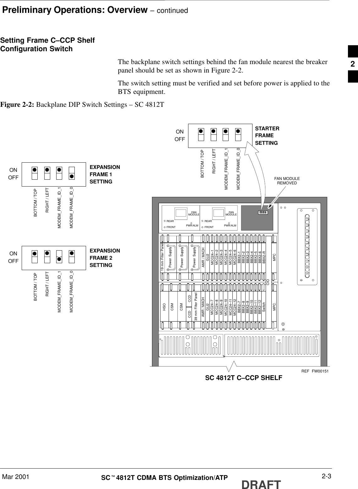
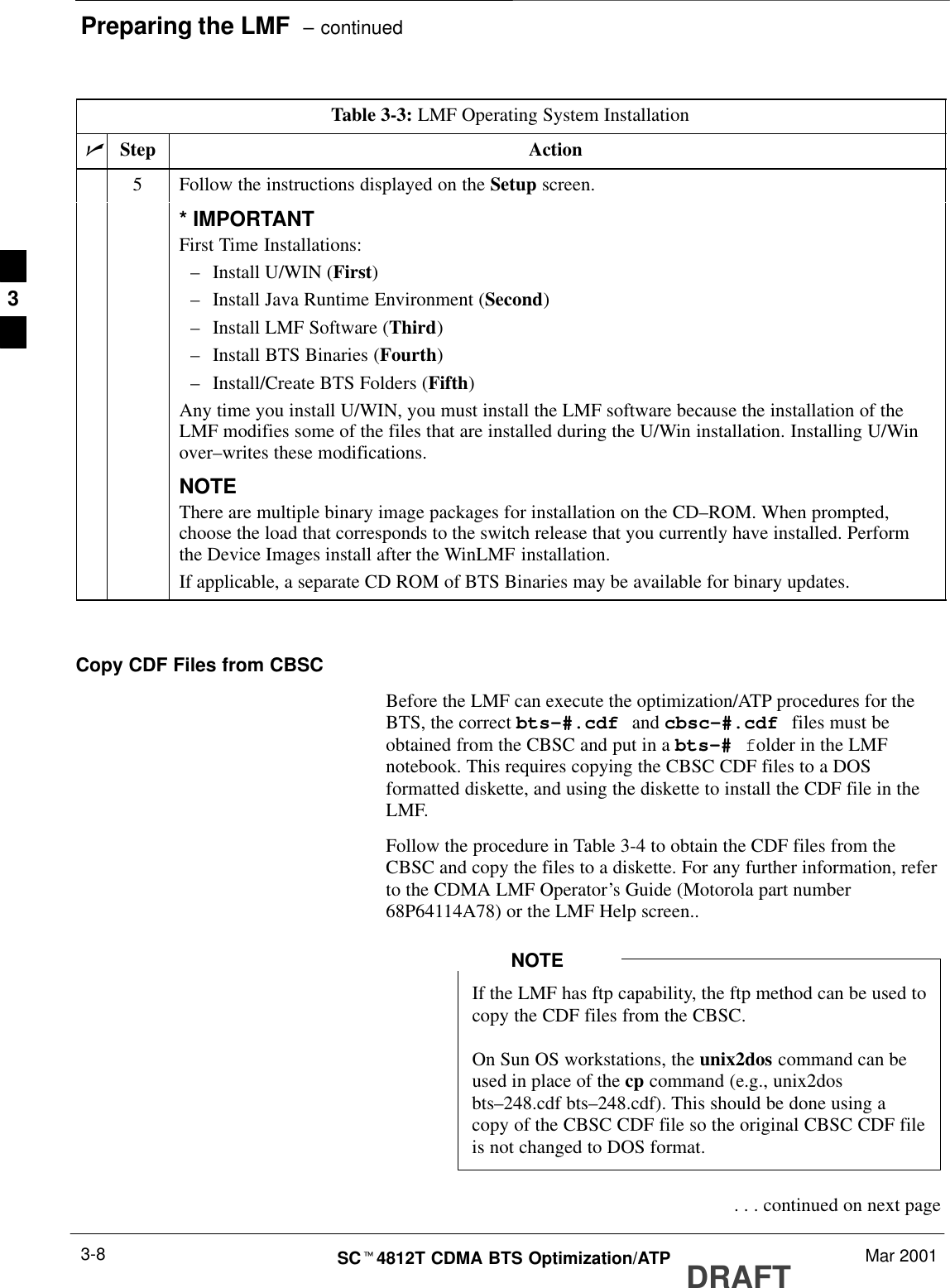
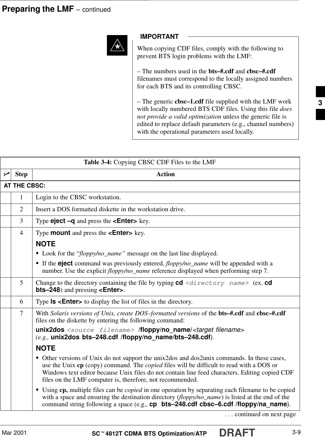
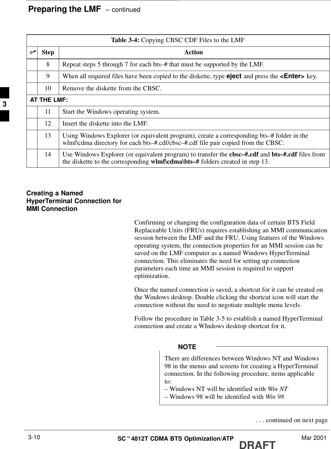
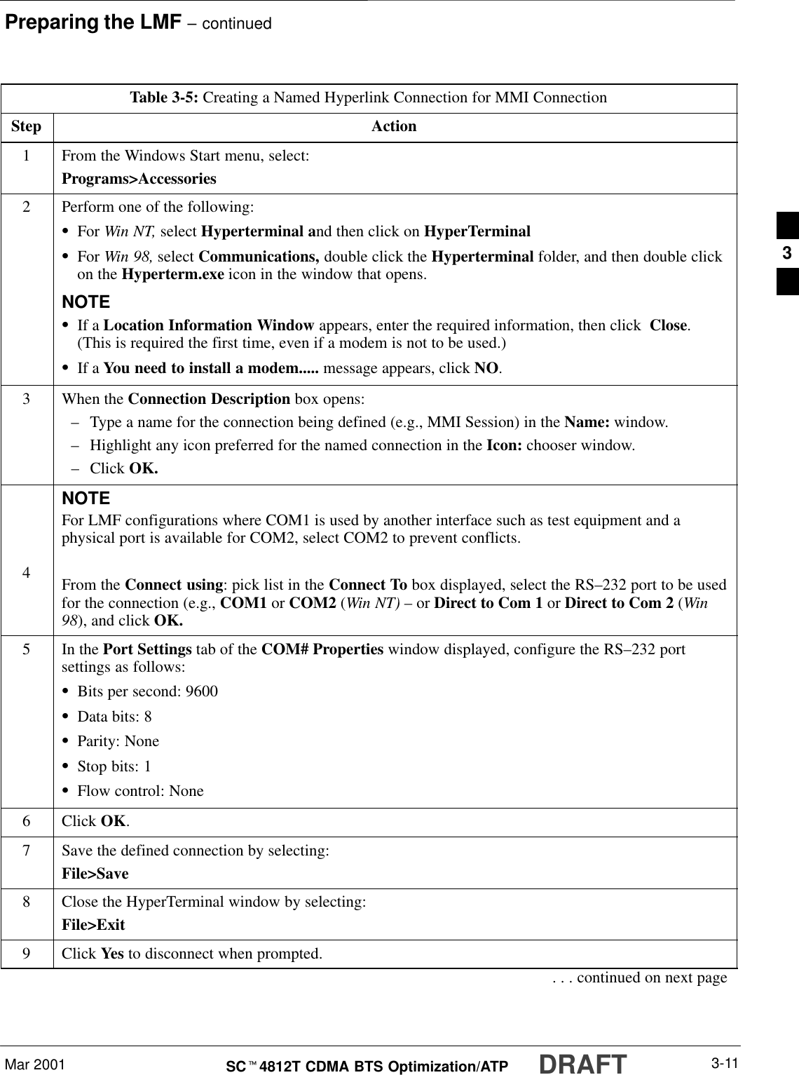
Nokia Solutions and Networks T6BN1 CDMA Base Station User Manual IHET6BN1 Part 2 of 3

Nokia Solutions and Networks CDMA Base Station IHET6BN1 Part 2 of 3

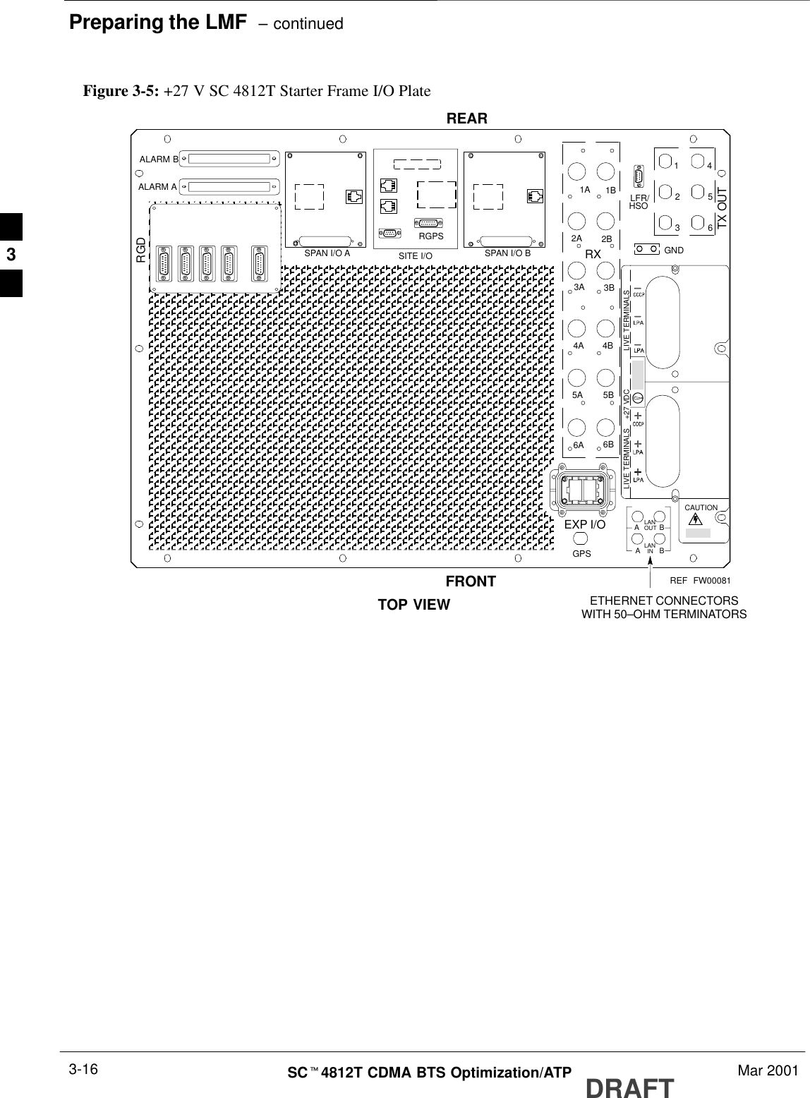
IHET6BN1 User Manual Part 2 of 3

Frame Module Location & Identification – continuedMar 2001 1-23SCt4812T CDMA BTS Optimization/ATP DRAFTFigure 1-8: +27 V SC 4812T Expansion Frame I/O PlateOUTLANINLANABABGPSEXP INSPAN I/O A SITE I/O SPAN I/O BLFR/ALARM B4GND56123TX OUTFRONTREARSPAN I/O ASPAN I/O BABCAUTIONLIVE TERMINALSLIVE TERMINALS    +27 VDCHSOEXP OUTABALARM AFW00082EXP INHOUSINGTRANSMITANTENNACONNECTORSEXP OUTHOUSING (ADDEDONLY WHENUSING SECONDEXPANSIONFRAME)SITE I/O LFR/HSORGDPOWERINPUTLANSPAN I/O SPAN I/ORGPSREF1
Frame Module Location & Identification – continuedDRAFTSCt4812T CDMA BTS Optimization/ATP Mar 20011-24Figure 1-9: –48 V SC 4812T Expansion Frame I/O PlateOUTLANINLANABABGPSEXP INSPAN I/O A SITE I/O SPAN I/O BLFRALARM B4GND56123TX OUTFRONTREARSPAN I/O ASPAN I/O BABCAUTIONLIVE TERMINALSHSO/EXP OUTABALARM AFW00480EXP INHOUSINGTRANSMITANTENNACONNECTORSEXP OUTHOUSING (ADDEDONLY WHENUSING SECONDEXPANSIONFRAME)SITE I/ORGDPOWERINPUTLANSPAN I/O SPAN I/O123123LIVE TERMINALS WIRED FOR –48 VDCSITE I/OHSO/LFRRF FILTER PORTS NOT USEDIN EXPANSION FRAMERGPSREF1
Frame Module Location & Identification – continuedMar 2001 1-25SCt4812T CDMA BTS Optimization/ATP DRAFTFigure 1-10: SC 4812T C–CCP Shelf19 mm Filler PanelPS–3AMR–1CSM–1CSM–238 mm Filler PanelAMR–2GLI2–1GLI2–2MCC24–6BBX2–1BBX2–2BBX2–3BBX2–4BBX2–5BBX2–6BBX2–RSwitchMPC/EMPC–1MPC/EMPC–2CIOBBX2–7BBX2–8BBX2–9BBX2–10BBX2–11BBX2–12MCC24–5MCC24–4MCC24–3MCC24–2MCC24–1MCC24–12MCC24–11MCC24–10MCC24–9MCC24–8MCC24–7PS–2PS–1CCD–2 CCD–1NOTE: MCCs may be MCC8Es, MCC24s, orMCC–1Xs. BBXs maybe BBX2s or BBX–1Xs.HSO/LFRFW00295REF1
Frame Module Location & Identification – continuedDRAFTSCt4812T CDMA BTS Optimization/ATP Mar 20011-26LPA1ALPA1BLPA1CLPA1DLPA3ALPA3BLPA3CLPA3DLPA2ALPA2BLPA2CLPA2DLPA4ALPA4BLPA4CLPA4DFANMODULE(TYPICAL)FILTERS /COMBINERS(2 TO 1 COMBINERSHOWN)NoteNo adjacent carriers may exist within the same TX filtercombiner.  “Adjacent” is defined as fc1 and fc2 being1.25 MHz apart (center–to–center).  “Non–adjacent” isdefined as fc1 and fc2 being >2.50 MHz apart(center–to–center).1234564–CARRIER CONFIGURATIONCARRIER13CARRIER24123456FW00296Figure 1-11: +27 V SC 4812T LPA Configuration – 4 Carrier with 2:1 Combiners1
Frame Module Location & Identification – continuedMar 2001 1-27SCt4812T CDMA BTS Optimization/ATP DRAFTFigure 1-12: –48 V SC 4812T LPA Configuration – 4 Carrier, 3–Sector with 2:1 CombinersLPA1ALPA1BNoteNo adjacent carriers may exist within the same TX filtercombiner.  “Adjacent” is defined as fc1 and fc2 being1.25 MHz apart (center–to–center).  “Non–adjacent” isdefined as fc1 and fc2 being >2.50 MHz apart(center–to–center).4–CARRIER CONFIGURATIONCARRIER CARRIERLPA1CLPA1DLPA3CLPA3DLPA2ALPA2BLPA2CLPA2DLPA4CLPA4DFW00481123456123 4123456LPA3ALPA3BLPA4ALPA4BFANMODULE(TYPICAL)FILTERS /COMBINERS(2 TO 1 COMBINERSHOWN)–48 VoltSC 4812T1
Frame Module Location & Identification – continuedDRAFTSCt4812T CDMA BTS Optimization/ATP Mar 20011-28Sector ConfigurationThere are a number of ways to configure the BTS frame. Table 1-3outlines the basic requirements. When carrier capacity is greater thantwo, a 2:1 or 4:1 cavity combiner must be used. For one or two carriers,bandpass filters or cavity combiners may be used, depending onsectorization and channel sequencing.Table 1-3: BTS Sector ConfigurationNumberof carriers Numberof sectors Channelspacing Filter requirements13 or 6 N/A Bandpass Filter, Cavity Combiner(2:1 or 4:1)2 6 Non–adjacent Cavity Combiner (2:1 Only)2 6 Adjacent Not supported in single frame2 3 Non–adjacent Cavity Combiner (2:1 or 4:1)2 3 Adjacent Bandpass Filter3,4 3 Non–adjacent Cavity Combiner (2:1 or 4:1)3,4 3 Adjacent Cavity Combiner (2:1 Only)In Table 1-4, BBXs may be BBX2s or BBX–1Xs.NOTE1
Frame Module Location & Identification – continuedMar 2001 1-29SCt4812T CDMA BTS Optimization/ATP DRAFTTable 1-4: Sector ConfigurationsConfig Ref. No. Description3–Sector/2–ADJACENT Carriers – The configuration below maps TX with optional 2:1 cavitycombiners for 3 sectors/2 carriers for adjacent channels. Note that 2:1 cavity combiners are used (6total).1TX1 TX2 TX3 TX4 TX5 TX6 Carrier#BBX–1 BBX–2 BBX–3 N/A N/A N/A 1N/A N/A N/A BBX–4 BBX–5 BBX–6 26–Sector/2–NON–ADJACENT Carriers – The configuration below maps TX with 2:1 cavitycombiners for 6 sectors/2 carriers for non–adjacent channels.2TX1 TX2 TX3 TX4 TX5 TX6 Carrier#BBX–1 BBX–2 BBX–3 BBX–4 BBX–5 BBX–6 1BBX–7 BBX–8 BBX–9 BBX–10 BBX–11 BBX–12 23–Sector/2–NON–ADJACENT Carriers – The configuration below maps TX with 2:1 cavitycombiners for 3 sectors/2 carriers for non–adjacent channels.3TX1 TX2 TX3 TX4 TX5 TX6 Carrier#BBX–1 BBX–2 BBX–3 N/A N/A N/A 1BBX–7 BBX–8 BBX–9 N/A N/A N/A 23–Sector/4–ADJACENT Carriers – The configuration below maps TX with 2:1 cavity combinersfor 3 sector/4 carriers for adjacent channels.TX1 TX2 TX3 TX4 TX5 TX6 Carrier#4BBX–1 BBX–2 BBX–3 N/A N/A N/A 1BBX–7 BBX–8 BBX–9 N/A N/A N/A 2N/A N/A N/A BBX–4 BBX–5 BBX–6 3N/A N/A N/A BBX–10 BBX–11 BBX–12 43–Sector / 2–ADJACENT Carriers – The configuration below maps TX with bandpass filters for3 sectors/2 carriers for adjacent channels.5TX1 TX2 TX3 TX4 TX5 TX6 Carrier#BBX–1 BBX–2 BBX–3 N/A N/A N/A 1N/A N/A N/A BBX–7 BBX–8 BBX–9 23–Sector/3 or 4–NON–ADJACENT Carriers – The configuration below maps TX with 4:1cavity combiners for 3 sectors/3 or 4 carriers for non–adjacent channels.TX1 TX2 TX3 TX4 TX5 TX6 Carrier#6BBX–1 BBX–2 BBX–3 N/A N/A N/A 1BBX–7 BBX–8 BBX–9 N/A N/A N/A 2BBX–4 BBX–5 BBX–6 N/A N/A N/A 3BBX–10 BBX–11 BBX–12 N/A N/A N/A 46–Sector/1–Carrier – The configuration below maps TX with either bandpass filters or 2:1 cavitycombiners for 6 sector/1 carrier.7TX1 TX2 TX3 TX4 TX5 TX6 Carrier#BBX–1 BBX–2 BBX–3 BBX–4 BBX–5 BBX–6 11
Frame Module Location & Identification – continuedDRAFTSCt4812T CDMA BTS Optimization/ATP Mar 20011-30Numbering456LPA 1ALPA 1BLPA 1CLPA 1DLPA 3CLPA 3ALPA 3BLPA 3DLPA 2DLPA 2CLPA 2BLPA 2ALPA 4BLPA 4ALPA 4CLPA 4DSector3 SectorSector3 Sector(6 Sector)Numbering2 to 1 Combiner3 Sector or 6 SectorC1, S1–3(C1, S1–3) C2, S1–3(C2, S1–3)C3, S1–3(C1, S4–6) C4, S1–3(C2, S4–6)(6 Sector)123456LPA 1ALPA 1BLPA 1CLPA 1DLPA 3CLPA 3ALPA 3BLPA 3DLPA 2DLPA 2CLPA 2BLPA 2ALPA 4BLPA 4ALPA 4CLPA 4DSectorNumbering SectorNumbering4 to 1 Combiner3 SectorC1, S1–3 C2, S1–3C3, S1–3 C4, S1–3123LPA 1ALPA 1BLPA 1CLPA 1D LPA 2DLPA 2CLPA 2BLPA 2ASector3 SectorNumbering Sector3 SectorNumberingDual Bandpass Filter3 Sector OnlyC1, S1–3 C2, S1–3123456LPA 1ALPA 1BLPA 1CLPA 1DLPA 3CLPA 3ALPA 3BLPA 3DSectorNumbering Dual Bandpass Filter6 SectorC1, S1–3C1, S4–62 Carrier Maximum 1 Carrier Only6 Sector123Figure 1-13: +27 V SC4812T LPA Configuration with Combiners/FiltersNote: See Table 1-4 ConfigurationReference Numbers 1, 2, 3, 4. Note: See Table 1-4 ConfigurationReference Number 6.Note: See Table 1-4 ConfigurationReference Number 5. Note: See Table 1-4 ConfigurationReference Number 7.FW002971
Frame Module Location & Identification – continuedMar 2001 1-31SCt4812T CDMA BTS Optimization/ATP DRAFTFigure 1-14: –48 V SC4812T LPA Configuration with Combiners/FiltersNote: See Table 1-4 ConfigurationReference Numbers 1, 2, 3, 4. Note: See Table 1-4 ConfigurationReference Number 6.Note: See Table 1-4 ConfigurationReference Number 5. Note: See Table 1-4 ConfigurationReference Number 7.REF FW00482415236NumberingSector3 SectorSector3 Sector(6 Sector)Numbering2 to 1 Combiner3 Sector or 6 SectorC1, S1–3(C1, S1–3) C2, S1–3(C2, S1–3)C3, S1–3(C1, S4–6) C4, S1–3(C2, S4–6)(6 Sector)LPA 1ALPA 1BLPA 1CLPA 1DLPA 3CLPA 3ALPA 3BLPA 3DLPA 2DLPA 2CLPA 2BLPA 2ALPA 4BLPA 4ALPA 4CLPA 4DSectorNumbering SectorNumbering4 to 1 Combiner3 SectorC1, S1–3 C2, S1–3C3, S1–3 C4, S1–3LPA 1ALPA 1B 13LPA 1CLPA 1DLPA 3CLPA 3ALPA 3BLPA 3DLPA 2DLPA 2CLPA 2BLPA 2ALPA 4BLPA 4ALPA 4CLPA 4D2LPA 1ALPA 1BLPA 1CLPA 1D LPA 2DLPA 2CLPA 2BLPA 2A45Sector3 SectorNumbering Sector3 SectorNumberingDual Bandpass Filter3 Sector OnlyC1, S1–3 C2, S1–32 Carrier Maximum21361524LPA 1ALPA 1BLPA 1CLPA 1DLPA 3CLPA 3ALPA 3BLPA 3DSectorNumberingDual Bandpass Filter6 SectorC1, S1–3C1, S4–61 Carrier Only6 Sector3 Sector3 Sector361
Frame Module Location & Identification – continuedDRAFTSCt4812T CDMA BTS Optimization/ATP Mar 20011-32Figure 1-15: –48 V BTS Power Conversion ShelfFW00501PS–6AMRPS–5PS–4PS–9PS–8PS–71C1A2A2C3C3A4A4CLPA1D1B2B2D3D3B4B4D3030303030303030FANMODULEPWR/ALMREARFRONTFANMODULEPWR/ALMREARFRONT1
Frame Module Location & Identification – continuedMar 2001 1-33SCt4812T CDMA BTS Optimization/ATP DRAFTFigure 1-16: CDMA (COBRA) RFDS LayoutAMR–B(RS–485 SERIAL)AMR–A(RS–485 SERIAL)Cobra RFDS external housing(Shown With Cover off)POWER SUPPLYON/OFF ROCKERSWITCHMMI PORT ANDPWR/ALARM LEDCobra RFDS Field Replaceable Unit (FRU)(shown removed from external housing)CHASSIS GNDPOWERCONNECTORCobra RFDS RF connectorpanel detail(shown from rear)ELECTRICAL GNDFRONT VIEWCASU 1CASU 2FWTICSUA ESN LABEL(FOR SC XXXX SERIES BTS)MMILEDSESN LABEL(FOR SC 6XX SERIES BTS)FW001381
Frame Module Location & Identification – continuedDRAFTSCt4812T CDMA BTS Optimization/ATP Mar 20011-34Notes1
Mar 2001 SCt4812T CDMA BTS Optimization/ATP DRAFTChapter 2: Preliminary OperationsTable of ContentsPreliminary Operations: Overview 2-1. . . . . . . . . . . . . . . . . . . . . . . . . . . . . . . . . . . Introduction 2-1. . . . . . . . . . . . . . . . . . . . . . . . . . . . . . . . . . . . . . . . . . . . . . Cell Site Types 2-1. . . . . . . . . . . . . . . . . . . . . . . . . . . . . . . . . . . . . . . . . . . . CDF 2-1. . . . . . . . . . . . . . . . . . . . . . . . . . . . . . . . . . . . . . . . . . . . . . . . . . . . Site Equipage Verification 2-1. . . . . . . . . . . . . . . . . . . . . . . . . . . . . . . . . . . Initial Installation of Boards/Modules 2-1. . . . . . . . . . . . . . . . . . . . . . . . . . Setting Frame C–CCP Shelf Configuration Switch 2-3. . . . . . . . . . . . . . . Pre–Power–up Tests 2-4. . . . . . . . . . . . . . . . . . . . . . . . . . . . . . . . . . . . . . . . . . . . . . Objective 2-4. . . . . . . . . . . . . . . . . . . . . . . . . . . . . . . . . . . . . . . . . . . . . . . . Test Equipment 2-4. . . . . . . . . . . . . . . . . . . . . . . . . . . . . . . . . . . . . . . . . . . Cabling Inspection 2-4. . . . . . . . . . . . . . . . . . . . . . . . . . . . . . . . . . . . . . . . . DC Power Pre-test (BTS Frame) 2-5. . . . . . . . . . . . . . . . . . . . . . . . . . . . . . DC Power Pre-test (RFDS) 2-11. . . . . . . . . . . . . . . . . . . . . . . . . . . . . . . . . . Initial Power–up Tests 2-12. . . . . . . . . . . . . . . . . . . . . . . . . . . . . . . . . . . . . . . . . . . . Power-up Procedures 2-12. . . . . . . . . . . . . . . . . . . . . . . . . . . . . . . . . . . . . . . Common Power Supply Verification 2-13. . . . . . . . . . . . . . . . . . . . . . . . . . . Initial Power-up (RFDS) 2-14. . . . . . . . . . . . . . . . . . . . . . . . . . . . . . . . . . . . Initial Power-up (BTS) 2-14. . . . . . . . . . . . . . . . . . . . . . . . . . . . . . . . . . . . . 2
Table of Contents  – continuedDRAFTSCt4812T CDMA BTS Optimization/ATP Mar 2001Notes2
Preliminary Operations: OverviewMar 2001 2-1SCt4812T CDMA BTS Optimization/ATP DRAFTIntroductionThis section first verifies proper frame equipage. This includes verifyingmodule placement, jumper, and dual in–line package (DIP) switchsettings against the site-specific documentation supplied for each BTSapplication. Next, pre-power up and initial power-up procedures arepresented.Cell Site TypesSites are configured as Omni with a maximum of 4 carriers, 3–sectoredwith a maximum of 4 carriers, and 6–sectored with a maximum of 2carriers. Each type has unique characteristics and must be optimizedaccordingly. For more information on the differences in site types, pleaserefer to the BTS/Modem Frame Hardware Installation manual.CDFThe Cell-site Data File (CDF) contains site type and equipage datainformation and passes it directly to the LMF during optimization. Thenumber of modem frames, C–CCP shelves, BBX boards, MCC boards(per cage), and linear power amplifier assignments are some of theequipage data included in the CDF.Be sure that the correct bts–#.cdf and cbsc–#.cdf files areused for the BTS. These should be the CDF files that areprovided for the BTS by the CBSC. Failure to use thecorrect CDF files can cause system errors. Failure to usethe correct CDF files to log into a live (traffic carrying)site can shut down the site.IMPORTANT*Site Equipage VerificationReview the site documentation. Match the site engineering equipage datato the actual boards and modules shipped to the site. Physically inspectand verify the equipment provided for the BTS or Modem frame andancillary equipment frame.Always wear a conductive, high impedance wrist strapwhile handling any circuit card/module to prevent damageby ESD. After removal, the card/module should be placedon a conductive surface or back into the anti–staticshipping bag.CAUTIONInitial Installation ofBoards/ModulesFollow the procedure in Table 2-1 to verify the initial installation ofboards/modules. . . . continued on next page2
Preliminary Operations: Overview  – continuedDRAFTSCt4812T CDMA BTS Optimization/ATP Mar 20012-2Table 2-1: Initial Installation of Boards/ModulesStep Action1Refer to the site documentation and install all boards and modules into the appropriate shelves asrequired. Verify they are NOT SEATED at this time.NOTEOn 800 MHz systems, the Switch Card has a configuration switch that must match the siteconfiguration (see Figure 2-1).2As the actual site hardware is installed, record the serial number of each module on a “Serial NumberChecklist” in the site logbook.Figure 2-1: Switch CardSwitch Card1234ONBTSMF3 Sector6 SectorJ1J2J3J4J5SHIELDSConfigurationSwitchNOTE:CONFIGURATION SWITCH ON800 MHZ SWITCH CARD ONLY.SHOWN FOR 3 SECTOR BTS.SWITCH 1 CHOOSES BTS OR MF.SWITCH 4 CHOOSES 3–SECTOR OR6 SECTOR. SWITCHES 2 & 3 ARE NOTUSED.FW003792
Preliminary Operations: Overview – continuedMar 2001 2-3SCt4812T CDMA BTS Optimization/ATP DRAFTSetting Frame C–CCP ShelfConfiguration SwitchThe backplane switch settings behind the fan module nearest the breakerpanel should be set as shown in Figure 2-2.The switch setting must be verified and set before power is applied to theBTS equipment.Figure 2-2: Backplane DIP Switch Settings – SC 4812T19 mm Filter PanelPower SupplyAMR / MACHHSOCSMCSM39 mm Filter PanelAMR / MACHGLI2GLI2MCC24–6BBX2–1BBX2–2BBX2–3BBX2–4BBX2–5BBX2–6BBX2–RSwitchMPCMPCCIOBBX2–7BBX2–8BBX2–9BBX2–10BBX2–11BBX2–12MCC24–5MCC24–4MCC24–3MCC24–2MCC24–1MCC24–12MCC24–11MCC24–10MCC24–9MCC24–8MCC24–7Power SupplyPower SupplyCCD CCDFANMODULEPWR/ALMREARFRONTFANMODULEPWR/ALMREARFRONTONOFFSC 4812T C–CCP SHELFFAN MODULEREMOVEDSTARTERFRAMESETTINGONOFFEXPANSIONFRAME 1SETTINGONOFFEXPANSIONFRAME 2SETTINGBOTTOM / TOPRIGHT / LEFTMODEM_FRAME_ID_1MODEM_FRAME_ID_0BOTTOM / TOPRIGHT / LEFTMODEM_FRAME_ID_1MODEM_FRAME_ID_0BOTTOM / TOPRIGHT / LEFTMODEM_FRAME_ID_1MODEM_FRAME_ID_0FW00151REF2
Pre–Power–up TestsDRAFTSCt4812T CDMA BTS Optimization/ATP Mar 20012-4ObjectiveThis procedure checks for any electrical short circuits and verifies theoperation and tolerances of the cellsite and BTS power supply units priorto applying power for the first time.Test EquipmentThe following test equipment is required to complete the pre–power–uptests:SDigital Multimeter (DMM)Always wear a conductive, high impedance wrist strapwhile handling the any circuit card/module to preventdamage by ESD.CAUTIONCabling InspectionUsing the site-specific documentation generated by Motorola SystemsEngineering, verify that the following cable systems are properlyconnected:SReceive RF cabling – up to 12 RX cablesSTransmit RF cabling – up to six TX cablesSGPSSLFRFor positive power applications (+27 V):SThe positive power cable is red.SThe negative power cable (ground) is black.For negative power applications (–48 V):SThe negative power cable is red or blue.SThe positive power cable (ground) is black.In all cases, the black power cable is at ground potential.IMPORTANT*2
Pre–Power–up Tests – continuedMar 2001 2-5SCt4812T CDMA BTS Optimization/ATP DRAFTDC Power Pre-test (BTS Frame) Before applying any power to the BTS frame, follow the procedure inTable 2-2 while referring to Figure 2-3 and Figure 2-4 for  +27 Vsystems or to Figure 2-5 and Figure 2-6 for –48 V systems to verifythere are no shorts in the BTS frame DC distribution system.Table 2-2: DC Power Pre–test (BTS Frame)Step Action1Physically verify that all DC power sources supplying power to the frame are OFF or disabled.2On each frame:SUnseat all circuit boards (except CCD and CIO cards) in the C–CCP shelf and LPA shelves, butleave them in their associated slots.SSet C–CCP shelf breakers to the OFF position by pulling out power distribution breakers (labeledC–CCP 1, 2, 3 on the +27 V BTS C–CCP power distribution panel and labeled POWER1,4,5,2,6,7,3,8,9 on the –48 V C–CCP power distribution panel).SSet LPA breakers to the OFF position by pulling out the LPA breakers (8 breakers, labeled 1A–1Bthrough 4C–4D – located on the C–CCP power distribution panel in the +27 V BTS or on thepower conversion shelf power distribution panel in the –48 V BTS).3Verify that the resistance from the power (+ or –) feed terminals with respect to the ground terminal onthe top of the frame measures > 500 Ω (see Figure 2-3).SIf reading is < 500 Ω, a short may exist somewhere in the DC distribution path supplied by thebreaker. Isolate the problem before proceeding. A reading > 3 MΩ could indicate an open (ormissing) bleeder resistor (installed across the filter capacitors behind the breaker panel).4Set the C–CCP (POWER) breakers to the ON position by pushing them IN one at a time. RepeatStep 3 after turning on each breaker.* IMPORTANT* IMPORTANTIf the ohmmeter stays at 0 Ω after inserting any board/module, a short probably exists in thatboard/module. Replace the suspect board/module and repeat the test. If test still fails, isolate theproblem before proceeding.5Insert and lock the DC/DC converter modules for the C–CCP shelf and into their associated slots oneat a time. Repeat Step 3 after inserting each module.SA typical response is that the ohmmeter steadily climbs in resistance as capacitors charge, finallyindicating approximately 500 Ω.! CAUTIONVerify the correct power/converter modules by observing the locking/retracting tabs appear as follows:– (in +27 V BTS C–CCP shelf)– (in –48 V BTS C–CCP shelf) STPN4045APWR CONV  CDMA RCVRSTPN4009PWR CONV  CDMA RCVR6Insert and lock all remaining circuit boards and modules into their associated slots in the C–CCP shelf.Repeat Step 3 after inserting and locking each board or module.SA typical response is that the ohmmeter steadily climbs in resistance as capacitors charge, stoppingat approximately 500 Ω... . . continued on next page2
Pre–Power–up  Tests – continuedDRAFTSCt4812T CDMA BTS Optimization/ATP Mar 20012-6Table 2-2: DC Power Pre–test (BTS Frame)Step Action7Set the LPA breakers ON by pushing them IN one at a time.Repeat Step 3 after turning on each breaker.SA typical response is that the ohmmeter will steadily climb in resistance as capacitors charge,stopping at approximately 500 Ω..8In the –48 V BTS, insert and lock the DC/DC LPA converter modules into their associated slots one ata time.Repeat Step 3 after inserting each module.SA typical response is that the ohmmeter steadily climbs in resistance as capacitors charge, finallyindicating approximately 500 Ω.! CAUTIONVerify the correct power/converter modules by observing the locking/retracting tabs appear as follows:– (in –48 V BTS power conversion shelf)STPN4044APWR CONV  LPA9Seat all LPA and associated LPA fan modules into their associated slots in the shelves one at a time.Repeat Step 3 after seating each LPA  and associated LPA fan module.SA typical response is that the ohmmeter will steadily climb in resistance as capacitors charge,stopping at approximately 500 Ω.. 2
Pre–Power–up Tests – continuedMar 2001 2-7SCt4812T CDMA BTS Optimization/ATP DRAFTPOWER INPUTTOP OF FRAMEBREAKER PANELLPABREAKERSC–CCPBREAKERS4GND56123TX OUTCAUTIONLIVE TERMINALSLIVE TERMINALS    +27 VDCLFR/HSOFigure 2-3: +27 V BTS DC Distribution Pre-testBreakering:S  Two LPAs on each trunking backplane breakered togetherS  Designed for peak LPA current of 15 amps (30 amp breakers)S  Unused TX paths do not need to be terminatedS  Single feed for C–CCPS  Dual feed for LPAFW002981D1B2B2D1C1A2A2C30303030303030303D3B4B4D3C3A4A4C505050123CCPLPAC . . . continued on next page2
Pre–Power–up  Tests – continuedDRAFTSCt4812T CDMA BTS Optimization/ATP Mar 20012-8Figure 2-4: +27 V SC 4812T BTS Starter FrameExpansion I/OHousingFor clarity, doors are not shown. FW00214Front CosmeticPanelPower InputConnectionTX Out (1 – 6)Span I/O BSpan I/O ASite I/ORX In (1A – 6Aand 1B – 6B)Exhaust RegionC–CCP CageBreakersCombinerSectionRGD (Needed forExpansion only)LPA Cage2
Pre–Power–up Tests – continuedMar 2001 2-9SCt4812T CDMA BTS Optimization/ATP DRAFTFigure 2-5: –48 V BTS DC Distribution Pre-test41527638P9OWER304040304040304040POWER INPUTTOP OF FRAMEC–CCP BREAKERLPABREAKER4GND56123TX OUTCAUTIONLIVE TERMINALSLIVE TERMINALS WIRED FOR –48 VDCLFRHSO/Breakering:S  Two LPAs on each trunking backplane breakered togetherS  Designed for peak LPA current of 15 amps (30 amp breakers)S  Unused TX paths do not need to be terminatedS  Single feed for C–CCPS  Dual feed for LPAFW004831231231C1A2A2C3C3A4A4CLPA1D1B2B2D3D3B4B4D30303030303030302
Pre–Power–up  Tests – continuedDRAFTSCt4812T CDMA BTS Optimization/ATP Mar 20012-10Figure 2-6: –48 V SC 4812T BTS Starter FrameFW00477Expansion I/OHousingFor clarity, doors are not shown.Front CosmeticPanelPower InputConnectionTX Out (1 – 6)Span I/O BSpan I/O ASite I/ORX In (1A – 6Aand 1B – 6B)Exhaust RegionC–CCP CageBreakersCombinerSectionRGD (Needed forExpansion only)LPA CagePowerConversionShelfBreakersAlarms2
Pre–Power–up Tests – continuedMar 2001 2-11SCt4812T CDMA BTS Optimization/ATP DRAFTDC Power Pre-test (RFDS)Before applying power to the RFDS, follow the steps in Table 2-3, whilereferring to Figure 2-7, to verify there are no shorts in the RFDS DCdistribution system, backplanes, or modules/boards. As of the date ofthis publication, the RFDS is not used with the –48 V BTS.Visual inspection of card placement and equipage for eachframe vs. site documentation must be completed, ascovered in Table 2-1, on page 2-2, before proceeding withthis test.IMPORTANT*Table 2-3: DC Power Pre-test (RFDS)Step Action1Physically verify that all DC/DC converters supplying the RFDS are OFF or disabled.2Set the input power rocker switch P1 to the OFF position (see Figure 2-7).3Verify the initial resistance from the power (+ or –) feed terminal with respect to ground terminalmeasures > 5 kΩ , then slowly begins to increase.SIf the initial reading is < 5 kΩ and remains constant, a short exists somewhere in the DCdistribution path supplied by the breaker. Isolate the problem before proceeding.4Set the input power rocker switch P1 to the ON position.Repeat Step 3.Figure 2-7: DC Distribution Pre-test (COBRA RFDS Detail)NOTE:Set the input power switch ON while measuring theresistance from the DC power –  with respect to thepower + terminal on the rear of the COBRA RFDS.INPUT POWERSWITCH (P1)FRONT OF COBRA RFDS(cut away view shown  for clarity)RFDS REARINTERCONNECT PANEL“–” CONNECTORPIN“+” CONNECTORPINCONNECTOR (MADEUP OF A HOUSINGAND TWO PINS)FW001392
Initial Power–up TestsDRAFTSCt4812T CDMA BTS Optimization/ATP Mar 20012-12Power-up ProceduresPotentially lethal voltage and current levels are routed tothe BTS equipment. This test must be performed with asecond person present, acting in a safety role. Remove allrings, jewelry, and wrist watches prior to beginning thistest.WARNINGDC Input PowerIn the tests to follow, power will first be verified at the input to eachBTS frame. After power is verified, cards and modules within the frameitself will be powered up and verified one at a time.Before applying any power, verify the correct power feed and returncables are connected between the power supply breakers and the powerconnectors at the top of each BTS frame. Verify correct cable positionreferring to Figure 2-3 on page 2-7 for +27 V systems and Figure 2-5 onpage 2-9 for –48 V systems.Always wear a conductive, high impedance wrist strapwhile handling any circuit card/module to prevent damageby ESD. Extreme care should be taken during the removaland installation of any card/module. After removal, thecard/module should be placed on a conductive surface orback into the anti–static bag in which it was shipped.CAUTIONFor positive power applications (+27 V):SThe positive power cable is red.SThe negative power cable (ground) is black.For negative power applications (–48 V):SThe negative power cable is red or blue.SThe positive power cable (ground) is black.In all cases, the black power cable is at ground potential.IMPORTANT*Motorola recommends that the DC input power cable used to connect theframe to the main DC power source conforms to the guidelines outlinedin Table 2-4. . . . continued on next page2
Initial Power–up Tests – continuedMar 2001 2-13SCt4812T CDMA BTS Optimization/ATP DRAFTTable 2-4: DC Input Power Cable GuidelinesMaximum Cable Length Wire Size30.38 m (100 ft) 107 mm2 (AWG #4/0)54.864 m (180 ft) 185 mm2 (350 kcmil)Greater that 54.864 m (180 ft) Not recommended*If Anderson SB350 style power connectors are used, makesure the connector adapters are securely attached to each ofthe BTS power feeds and returns. Also, make sure thecables have been  properly installed into each connector.IMPORTANTCommon Power SupplyVerificationThe procedure in Table 2-5 must be performed on any BTS frameconnected to a common power supply at the site after the common powersupply has been installed and verified per the power supply OEMsuggested procedures.Perform the following steps to verify the power input is withinspecification before powering up the individual cards/modules with theframes themselves.Table 2-5: Common Power Supply VerificationStep Action1Physically verify that all DC power sources supplying the frame are OFF or disabled.2On the RFDS (for +27 V systems only), set the input power switch P1 to the OFF position (seeFigure 2-7).3On each frame:SUnseat all circuit boards (except CCD and CIO cards) in the C–CCP shelf and LPA shelves, butleave them in their associated slots.SSet breakers to the OFF position by pulling out C–CCP and LPA breakers (see Figure 2-3 onpage 2-7 or Figure 2-5 on page 2-9 for breaker panel layout if required).–C–CCP shelf breakers are labeled CCCP–1, 2, 3 in the +27 V BTS and labeled POWER1,4,5,2,6,7,3,8,9 in the –48 V BTS.–LPA breakers are labeled 1A–1B through 4C–4D.4Inspect input cables, verify correct input power polarity via decal on top of frame (+27 Vdc or–48 Vdc).5Apply power to BTS frames, one at a time, by setting the appropriate breaker in the power supply thatsupplies the frame to the ON position.6After power is applied to each frame, use a digital voltmeter to verify power supply output voltages atthe top of each BTS frame are within specifications: +27.0 Vdc or –48 Vdc nominal.2
Initial Power–up Tests – continuedDRAFTSCt4812T CDMA BTS Optimization/ATP Mar 20012-14Initial Power-up (RFDS)The procedure in Table 2-6 must be performed on the RFDS after inputpower from the common power supply has been verified. Perform thefollowing steps to apply initial power to the cards/modules within theframe itself, verifying that each is operating within specification.Visual inspection of card placement and equipage for eachframe vs. site documentation must be completed, ascovered in Table 2-1, on page 2-2, before proceeding withthis test.IMPORTANT*Table 2-6: Initial Power-up (RFDS)Step Action1On the RFDS, set the input power rocker switch (P1) to the ON position (see Figure 2-7).2Verify power supply output voltages (at the top of BTS frame), using a digital voltmeter, are withinspecifications: +27.0 V nominal.Initial Power-up (BTS)The procedure must be performed on each frame after input power fromthe common power supply has been verified. Follow the steps inTable 2-7 to apply initial power to the cards/modules within the frameitself, verifying that each is operating within specification.Table 2-7: Initial Power–up (BTS)Step Action1At the BTS, set the C–CCP (POWER) power distribution breakers (see Figure 2-3 on page 2-7 orFigure 2-5 on page 2-9) to the ON position by pushing in the breakers.2Insert the C–CCP fan modules. Observe that the fan modules come on line.3! CAUTIONVerify the correct power/converter modules by observing the locking/retracting tabs appear as follows:–(in +27 V BTS C–CCP shelf)–(in –48 V BTS C–CCP shelf)–(in –48 V BTS power conversion shelf)Insert and lock the converter/power supplies into their associated slots one at a time.•If no boards have been inserted, all three PWR/ALM LEDs would indicate RED to notify the userthat there is no load on the power supplies.–If the LED is RED, do not be alarmed. After Step 4 is performed, the LEDs should turn GREEN;if not, then a faulty converter/power supply module is indicated and should be replaced beforeproceeding.STPN 4045APWR CONV  CDMA RCVRSTPN 4044APWR CONV  LPASTPN4009PWR CONV  CDMA RCVR4Seat and lock all remaining circuit cards and modules in the C–CCP shelf into their associated slots.. . . continued on next page2
Initial Power–up Tests – continuedMar 2001 2-15SCt4812T CDMA BTS Optimization/ATP DRAFTTable 2-7: Initial Power–up (BTS)Step Action5Seat the first equipped LPA module pair into the assigned slot in the upper LPA shelf including LPAfan.SIn +27 V systems, observe that the LPA internal fan comes on line.6Repeat step 5 for all remaining LPAs.7Set the LPA breakers to the ON position (per configuration) by pushing them IN one at a time. SeeFigure 1-13 on page 1-30 or Figure 1-14 on page 1-31 for configurations and Figure 2-3 on page 2-7or Figure 2-5 on page 2-9 for LPA breaker panel layout.On +27 V frames, engage (push) LPA circuit breakers.SConfirm LEDs on LPAs light.On –48 V frames, engage (push) LPA PS circuit breakers.SConfirm LPA PS fans start.SConfirm LEDs on –48 V power converter boards light.SConfirm LPA fans start.SConfirm LEDs on LPAs light.8After all cards/modules have been seated and verified, use a digital voltmeter to verify power supplyoutput voltages at the top of the frame remain within specifications: +27.0 Vdc or –48 Vdc nominal.9Repeat Steps 1 through 8 for additional co–located frames (if equipped). 2
Initial Power–up Tests – continuedDRAFTSCt4812T CDMA BTS Optimization/ATP Mar 20012-16Notes2
Mar 2001 SCt4812T CDMA BTS Optimization/ATP DRAFTChapter 3: Optimization/CalibrationTable of ContentsOptimization/Calibration – Introduction 3-1. . . . . . . . . . . . . . . . . . . . . . . . . . . . . . Introduction 3-1. . . . . . . . . . . . . . . . . . . . . . . . . . . . . . . . . . . . . . . . . . . . . . Optimization Process 3-1. . . . . . . . . . . . . . . . . . . . . . . . . . . . . . . . . . . . . . . Cell Site Types 3-2. . . . . . . . . . . . . . . . . . . . . . . . . . . . . . . . . . . . . . . . . . . . Cell–Site Data File 3-2. . . . . . . . . . . . . . . . . . . . . . . . . . . . . . . . . . . . . . . . . BTS System Software Download 3-3. . . . . . . . . . . . . . . . . . . . . . . . . . . . . Site Equipage Verification 3-3. . . . . . . . . . . . . . . . . . . . . . . . . . . . . . . . . . . Isolate Span Lines/Connect LMF 3-4. . . . . . . . . . . . . . . . . . . . . . . . . . . . . . . . . . . . Isolate BTS from T1/E1 Spans 3-4. . . . . . . . . . . . . . . . . . . . . . . . . . . . . . . LMF to BTS Connection 3-5. . . . . . . . . . . . . . . . . . . . . . . . . . . . . . . . . . . . Preparing the LMF 3-7. . . . . . . . . . . . . . . . . . . . . . . . . . . . . . . . . . . . . . . . . . . . . . . Overview 3-7. . . . . . . . . . . . . . . . . . . . . . . . . . . . . . . . . . . . . . . . . . . . . . . . LMF Operating System Installation 3-7. . . . . . . . . . . . . . . . . . . . . . . . . . . Copy CDF Files from CBSC 3-8. . . . . . . . . . . . . . . . . . . . . . . . . . . . . . . . . Creating a Named HyperTerminal Connection for MMI Connection 3-10. . Folder Structure Overview 3-13. . . . . . . . . . . . . . . . . . . . . . . . . . . . . . . . . . . Pinging the Processors 3-14. . . . . . . . . . . . . . . . . . . . . . . . . . . . . . . . . . . . . . Using CDMA LMF 3-18. . . . . . . . . . . . . . . . . . . . . . . . . . . . . . . . . . . . . . . . . . . . . . Basic LMF Operation 3-18. . . . . . . . . . . . . . . . . . . . . . . . . . . . . . . . . . . . . . Graphical User Interface Overview 3-18. . . . . . . . . . . . . . . . . . . . . . . . . . . . Command Line Interface Overview 3-19. . . . . . . . . . . . . . . . . . . . . . . . . . . . Logging into a BTS 3-20. . . . . . . . . . . . . . . . . . . . . . . . . . . . . . . . . . . . . . . . Logging Out 3-22. . . . . . . . . . . . . . . . . . . . . . . . . . . . . . . . . . . . . . . . . . . . . . Establishing an MMI Communication Session 3-24. . . . . . . . . . . . . . . . . . . Download the BTS 3-25. . . . . . . . . . . . . . . . . . . . . . . . . . . . . . . . . . . . . . . . . . . . . . . Download the BTS – Overview 3-25. . . . . . . . . . . . . . . . . . . . . . . . . . . . . . . Download Code to Devices 3-26. . . . . . . . . . . . . . . . . . . . . . . . . . . . . . . . . . Download Code and Data to Non–MGLI2 Devices 3-28. . . . . . . . . . . . . . . Select CSM Clock Source 3-28. . . . . . . . . . . . . . . . . . . . . . . . . . . . . . . . . . . Enable CSMs 3-29. . . . . . . . . . . . . . . . . . . . . . . . . . . . . . . . . . . . . . . . . . . . . Enable MCCs 3-31. . . . . . . . . . . . . . . . . . . . . . . . . . . . . . . . . . . . . . . . . . . . . Enable Redundant GLIs 3-31. . . . . . . . . . . . . . . . . . . . . . . . . . . . . . . . . . . . . CSM System Time/GPS and LFR/HSO Verification 3-32. . . . . . . . . . . . . . . . . . . . . CSM & LFR Background 3-32. . . . . . . . . . . . . . . . . . . . . . . . . . . . . . . . . . . Low Frequency Receiver/High Stability Oscillator 3-33. . . . . . . . . . . . . . . Front Panel LEDs 3-33. . . . . . . . . . . . . . . . . . . . . . . . . . . . . . . . . . . . . . . . . 3
Table of Contents  – continuedDRAFTSCt4812T CDMA BTS Optimization/ATP Mar 2001Null Modem Cable 3-34. . . . . . . . . . . . . . . . . . . . . . . . . . . . . . . . . . . . . . . . CSM Frequency Verification 3-34. . . . . . . . . . . . . . . . . . . . . . . . . . . . . . . . . Test Equipment Setup: GPS & LFR/HSO Verification 3-34. . . . . . . . . . . . . GPS Initialization/Verification 3-36. . . . . . . . . . . . . . . . . . . . . . . . . . . . . . . . LFR Initialization/Verification 3-39. . . . . . . . . . . . . . . . . . . . . . . . . . . . . . . . HSO Initialization/Verification 3-42. . . . . . . . . . . . . . . . . . . . . . . . . . . . . . . Test Equipment Set–up 3-43. . . . . . . . . . . . . . . . . . . . . . . . . . . . . . . . . . . . . . . . . . . . Connecting Test Equipment to the BTS 3-43. . . . . . . . . . . . . . . . . . . . . . . . Supported Test Sets 3-43. . . . . . . . . . . . . . . . . . . . . . . . . . . . . . . . . . . . . . . . Test Equipment Reference Chart 3-44. . . . . . . . . . . . . . . . . . . . . . . . . . . . . . Equipment Warm-up 3-45. . . . . . . . . . . . . . . . . . . . . . . . . . . . . . . . . . . . . . . Calibrating Cables 3-45. . . . . . . . . . . . . . . . . . . . . . . . . . . . . . . . . . . . . . . . . Test Set Calibration 3-53. . . . . . . . . . . . . . . . . . . . . . . . . . . . . . . . . . . . . . . . . . . . . . . Test Set Calibration Background 3-53. . . . . . . . . . . . . . . . . . . . . . . . . . . . . . Purpose of Test set Calibration 3-53. . . . . . . . . . . . . . . . . . . . . . . . . . . . . . . Selecting Test Equipment 3-54. . . . . . . . . . . . . . . . . . . . . . . . . . . . . . . . . . . Manually Selecting Test Equipment in a Serial Connection Tab 3-54. . . . . Automatically Selecting Test Equipment in a Serial Connection Tab 3-55. . Calibrating Test Equipment 3-56. . . . . . . . . . . . . . . . . . . . . . . . . . . . . . . . . . Calibrating Cables 3-56. . . . . . . . . . . . . . . . . . . . . . . . . . . . . . . . . . . . . . . . . Calibrating Cables with a CDMA Analyzer 3-57. . . . . . . . . . . . . . . . . . . . . Calibrating TX Cables Using a Signal Generator andSpectrum Analyzer 3-58. . . . . . . . . . . . . . . . . . . . . . . . . . . . . . . . . . . . . . . . Calibrating RX Cables Using a Signal Generator andSpectrum Analyzer 3-59. . . . . . . . . . . . . . . . . . . . . . . . . . . . . . . . . . . . . . . . Setting Cable Loss Values 3-61. . . . . . . . . . . . . . . . . . . . . . . . . . . . . . . . . . . Setting TX Coupler Loss Value 3-62. . . . . . . . . . . . . . . . . . . . . . . . . . . . . . . Bay Level Offset Calibration 3-63. . . . . . . . . . . . . . . . . . . . . . . . . . . . . . . . . . . . . . . Introduction to Bay Level Offset Calibration 3-63. . . . . . . . . . . . . . . . . . . . RF Path Bay Level Offset Calibration 3-63. . . . . . . . . . . . . . . . . . . . . . . . . . When to Calibrate BLOs 3-63. . . . . . . . . . . . . . . . . . . . . . . . . . . . . . . . . . . . TX Path Calibration 3-64. . . . . . . . . . . . . . . . . . . . . . . . . . . . . . . . . . . . . . . . BLO Calibration Data File 3-65. . . . . . . . . . . . . . . . . . . . . . . . . . . . . . . . . . Test Equipment Setup: RF Path Calibration 3-67. . . . . . . . . . . . . . . . . . . . . TX Path Calibration 3-68. . . . . . . . . . . . . . . . . . . . . . . . . . . . . . . . . . . . . . . . Download BLO Procedure 3-70. . . . . . . . . . . . . . . . . . . . . . . . . . . . . . . . . . . Calibration Audit Introduction 3-70. . . . . . . . . . . . . . . . . . . . . . . . . . . . . . . TX Path Audit 3-71. . . . . . . . . . . . . . . . . . . . . . . . . . . . . . . . . . . . . . . . . . . . TX Audit Test 3-71. . . . . . . . . . . . . . . . . . . . . . . . . . . . . . . . . . . . . . . . . . . . All Cal/Audit Test 3-72. . . . . . . . . . . . . . . . . . . . . . . . . . . . . . . . . . . . . . . . . Create CAL File 3-74. . . . . . . . . . . . . . . . . . . . . . . . . . . . . . . . . . . . . . . . . . . RFDS Setup and Calibration 3-75. . . . . . . . . . . . . . . . . . . . . . . . . . . . . . . . . . . . . . . RFDS Description 3-75. . . . . . . . . . . . . . . . . . . . . . . . . . . . . . . . . . . . . . . . . RFDS Parameter Settings 3-76. . . . . . . . . . . . . . . . . . . . . . . . . . . . . . . . . . . RFDS TSU NAM Programming 3-78. . . . . . . . . . . . . . . . . . . . . . . . . . . . . . Explanation of Parameters used when Programming the TSU NAM 3-78. . Valid NAM Ranges 3-79. . . . . . . . . . . . . . . . . . . . . . . . . . . . . . . . . . . . . . . . 3
Table of Contents  – continuedMar 2001 SCt4812T CDMA BTS Optimization/ATP DRAFTSet Antenna Map Data 3-80. . . . . . . . . . . . . . . . . . . . . . . . . . . . . . . . . . . . . . Set RFDS Configuration Data 3-81. . . . . . . . . . . . . . . . . . . . . . . . . . . . . . . . RFDS Calibration 3-82. . . . . . . . . . . . . . . . . . . . . . . . . . . . . . . . . . . . . . . . . Program TSU NAM 3-83. . . . . . . . . . . . . . . . . . . . . . . . . . . . . . . . . . . . . . . . BTS Redundancy/Alarm Testing 3-85. . . . . . . . . . . . . . . . . . . . . . . . . . . . . . . . . . . . Objective 3-85. . . . . . . . . . . . . . . . . . . . . . . . . . . . . . . . . . . . . . . . . . . . . . . . Test Equipment 3-85. . . . . . . . . . . . . . . . . . . . . . . . . . . . . . . . . . . . . . . . . . . Redundancy/Alarm Test 3-85. . . . . . . . . . . . . . . . . . . . . . . . . . . . . . . . . . . . Test Equipment Setup 3-86. . . . . . . . . . . . . . . . . . . . . . . . . . . . . . . . . . . . . . Power Supply Redundancy 3-87. . . . . . . . . . . . . . . . . . . . . . . . . . . . . . . . . . Miscellaneous Alarm/Redundancy Tests 3-89. . . . . . . . . . . . . . . . . . . . . . . . BBX Redundancy 3-91. . . . . . . . . . . . . . . . . . . . . . . . . . . . . . . . . . . . . . . . . CSM, GPS, & LFR/HSO Redundancy/Alarm Tests 3-92. . . . . . . . . . . . . . . LPA Redundancy Test 3-95. . . . . . . . . . . . . . . . . . . . . . . . . . . . . . . . . . . . . . MGLI/GLI Redundancy Test 3-96. . . . . . . . . . . . . . . . . . . . . . . . . . . . . . . . . BTS Alarms Testing 3-97. . . . . . . . . . . . . . . . . . . . . . . . . . . . . . . . . . . . . . . . . . . . . . Alarm Test Overview 3-97. . . . . . . . . . . . . . . . . . . . . . . . . . . . . . . . . . . . . . . Alarm Reporting Display 3-97. . . . . . . . . . . . . . . . . . . . . . . . . . . . . . . . . . . . Purpose 3-98. . . . . . . . . . . . . . . . . . . . . . . . . . . . . . . . . . . . . . . . . . . . . . . . . Test Equipment 3-98. . . . . . . . . . . . . . . . . . . . . . . . . . . . . . . . . . . . . . . . . . . CDI Alarm Input Verification with Alarms Test Box 3-99. . . . . . . . . . . . . . CDI Alarm Input Verification without Alarms Test Box 3-102. . . . . . . . . . . Pin and Signal Information for Alarm Connectors 3-103. . . . . . . . . . . . . . . . 3
Table of Contents  – continuedDRAFTSCt4812T CDMA BTS Optimization/ATP Mar 2001Notes3
Optimization/Calibration – IntroductionMar 2001 3-1SCt4812T CDMA BTS Optimization/ATP DRAFTIntroductionThis section describes procedures for isolating the BTS from the spanlines, preparing and using the LMF, downloading system operatingsoftware, CSM reference verification/optimization, set up and calibrationof the supported test equipment, transmit/receive path verification, usingthe RFDS, and verifying the customer defined alarms and relay contactsare functioning properly.Before using the LMF, use an editor to view the”CAVEATS” section in the ”readme.txt” file in the c:\wlmffolder for any applicable information.IMPORTANT*Optimization ProcessAfter a BTS is physically installed and the preliminary operations(power up) have been completed, the LMF is used to calibrate andoptimize the BTS. Motorola recommends that the optimization beaccomplished as follows:1. Download MGLI2–1 with code and data and then enable MGLI2–1.2. Use the status function and verify that all of the installed devices ofthe following types respond with status information: CSM, BBX,GLI2, MCC, and TSU (if RFDS is installed). If a device is installedand powered up but is not responding and is colored gray in the BTSdisplay, the device is not listed in the CDF file. The CDF file willhave to be corrected before the device can be accessed by the LMF.3. Download code and data to all devices of the following types:–CSM–BBX (may be BBX2 or BBX–1X)–GLI2 (other than MGLI2–1)–MCC (may be MCC–8E, MCC24, or MCC–1X)4. Download the RFDS TSIC (if installed).5. Verify the operation of the GPS and HSO signals.6. Enable the following devices (in the order listed):–Secondary CSM–Primary CSM–All MCCs7. Connect the required test equipment for a full optimization.8. Select the test equipment.9. Calibrate the TX and RX test cables if they have not previously beencalibrated using the CDMA LMF that is going to be used for theoptimization/calibration. The cable calibration values can also beentered manually. . . . continued on next page3
Optimization/Calibration – Introduction – continuedDRAFTSCt4812T CDMA BTS Optimization/ATP Mar 20013-210. Select all of the BBXs and all of the MCCs, and use the fulloptimization function. The full optimization function performs TXcalibration, BLO download, TX audit, all TX tests, and all RX testsfor all selected devices.11. If the TX calibration fails, repeat the full optimization for any failedpaths.12. If the TX calibration fails again, correct the problem that caused thefailure and repeat the full optimization for the failed path.13. If the TX calibration and audit portion of the full optimization passesfor a path but some of the TX or RX tests fail, correct the problemthat caused the failure and run the individual tests as required untilall TX and RX tests have passed for all paths.Cell Site TypesSites are configured as Omni/Omni or Sector/Sector (TX/RX). Each typehas unique characteristics and must be optimized accordingly.For more information on the differences in site types,please refer to the applicable BTS/Modem Frame HardwareInstallation and Functional Hardware Descriptionmanuals.NOTECell–Site Data FileThe Cell–SiteData File (CDF) contains information that defines the BTSand data used to download files to the devices. A CDF file must beplaced in the applicable BTS folder before the LMF can be used to loginto that BTS. CDF files are normally obtained from the CBSC using afloppy disk. A file transfer protocol (ftp) method can be used if the LMFcomputer has that capability. The CDF includes the following information:SDownload instructions and protocolSSite specific equipage informationSC–CCP shelf allocation plan–BBX equipage (based on cell–site type) including redundancy–CSM equipage including redundancy–MCC (MCC24E, MCC8E, or MCC–1X) channel element allocationplan. This plan indicates how the C–CCP shelf is configured, andhow the paging, synchronization, traffic, and access channelelements (and associated gain values) are assigned among the (up to12) MCCs in the shelf.SCSM equipage including redundancy . . . continued on next page3
Optimization/Calibration – Introduction – continuedMar 2001 3-3SCt4812T CDMA BTS Optimization/ATP DRAFTSEffective Rated Power (ERP) table for all TX channels to antennasrespectively. Motorola System Engineering specifies the ERP of atransmit antenna based on site geography, antenna placement, andgovernment regulations. Working from this ERP requirement, theantenna gain, (dependent on the units of measurement specified) andantenna feed line loss can be combined to determine the requiredpower at the top of the BTS frame. The corresponding BBX outputlevel required to achieve that power level on any channel/sector canalso be determined.Refer to the CDMA LMF Operator’s Guide, 68P64114A78,for additional information on the layout of the LMFdirectory structure (including CDF file locations andformats).NOTEBTS System SoftwareDownloadBTS system software must be successfully downloaded to the BTSprocessor boards before optimization can be performed. BTS operatingcode is loaded from the LMF computer terminal.Before using the LMF for optimization/ATP, the correctbts–#.cdf and cbsc–#.cdf files for the BTS must beobtained from the CBSC and put in a bts–# folder in theLMF. Failure to use the correct CDF files can cause wrongresults. Failure to use the correct CDF files to log into alive (traffic carrying) site can shut down the site.IMPORTANT*The CDF is normally obtained from the CBSC on a DOS formatteddiskette, or through a file transfer protocol (ftp) if the LMF computer hasftp capability. Refer to the CDMA LMF Operator’s Guide, or the LMFHelp screen, for the procedure.Site Equipage VerificationIf you have not already done so, use an editor to view the CDF, andreview the site documentation. Verify the site engineering equipage datain the CDF matches the actual site hardware using a CDF conversiontable.Always wear a conductive, high impedance wrist strapwhile handling any circuit card/module to prevent damageby ESD. Extreme care should be taken during the removaland installation of any card/module. After removal, thecard/module should be placed on a conductive surface orback into the anti–static bag in which it was shipped.CAUTION3
Isolate Span Lines/Connect LMFDRAFTSCt4812T CDMA BTS Optimization/ATP Mar 20013-4Isolate BTS from T1/E1 SpansAt active sites, the OMC/CBSC must disable the BTS andplace it out of service (OOS). DO NOT remove the 50–pinTELCO cable connected to the BTS frame site I/O boardJ1 connector until the OMC/CBSC has disabled the BTS!IMPORTANT*Each frame is equipped with one Site I/O and two Span I/O boards. TheSpan I/O J1 connector provides connection of 25 pairs of wire. A GLI2card can support up to six spans. In the SC 4812T configuration, the oddspans (1, 3, and 5) terminate on the Span ”A” I/O; and the even spans (2,4, and 6) terminate on the Span ”B” I/O.Before connecting the LMF to the frame LAN, the OMC/CBSC mustdisable the BTS and place it OOS to allow the LMF to control theCDMA BTS. This prevents the CBSC from inadvertently sendingcontrol information to the CDMA BTS during LMF based tests. Refer toFigure 3-1 and Figure 3-2 as required.Table 3-1: T1/E1 Span IsolationStep Action1From the OMC/CBSC, disable the BTS and place it OOS. Refer to SC OMC–R/CBSC SystemOperator Procedures.–The T1/E1 span 50–pin TELCO cable connected to the BTS frame SPAN I/O board J1 connectorcan be removed from both Span I/O boards, if equipped, to isolate the spans.NOTEIf a third party is used for span connectivity, the third party must be informed before disconnecting thespan line.* IMPORTANTVerify that you remove the SPAN cable, not the “MODEM/TELCO” connector.3
Isolate Span Lines/Connect LMF – continuedMar 2001 3-5SCt4812T CDMA BTS Optimization/ATP DRAFTFigure 3-1: Span I/O Board T1 Span Isolation50–PIN TELCOCONNECTORSREMOVEDSPAN A CONNECTOR(TELCO) INTERFACETO SPAN LINESSPAN B CONNECTOR(TELCO) INTERFACETO SPAN LINESTOP of Frame (Site I/O and Span I/O boards)RS–232 9–PIN SUB DCONNECTOR SERIALPORT FOR EXTERNALDIAL UP MODEMCONNECTION (IF USED)FW00299LMF to BTS ConnectionThe LMF is connected to the LAN A or B connector located on the leftside of the frame’s lower air intake grill, behind the LAN Cable Accessdoor (see Figure 3-2).Table 3-2: LMF to BTS ConnectionStep Action1To gain access to the connectors on the BTS, open the LAN Cable Access door, then pull apart theVelcro tape covering the BNC “T” connector (see Figure 3-2).2Connect the LMF to the LAN A BNC connector via PCMCIA Ethernet Adapter with an unshieldedtwisted–pair (UTP) Adapter and 10BaseT/10Base2 converter (powered by an external AC/DCtransformer).–If there is no login response, connect the LMF to the LAN B connector.–If there is still no login response, see Table 6-1, Login Failure Troubleshooting Procedures.NOTE–Xircom Model PE3–10B2 or equivalent can also be used to interface the LMF Ethernetconnection to the frame connected to the PC parallel port, powered by an external AC/DCtransformer. In this case, the BNC cable must not exceed 91 cm (3 ft) in length.* IMPORTANT–The LAN shield is isolated from chassis ground. The LAN shield (exposed portion of BNCconnector) must not touch the chassis during optimization.3
Isolate Span Lines/Connect LMF – continuedDRAFTSCt4812T CDMA BTS Optimization/ATP Mar 20013-6Figure 3-2: LMF Connection DetailNOTE:Open LAN CABLE ACCESSdoor. Pull apart Velcro tape andgain access to the LAN A or LANB LMF BNC connector.LMF BNC “T” CONNECTIONSON LEFT SIDE OF FRAME(ETHERNET “A” SHOWN;ETHERNET “B” COVEREDWITH VELCRO TAPE)LMF COMPUTERTERMINAL WITHMOUSE PCMCIA ETHERNETADPATER & ETHERNETUTP ADAPTER10BASET/10BASE2CONVERTER CONNECTSDIRECTLY TO BNC T   115 VAC POWERCONNECTION FW00140UNIVERSAL TWISTEDPAIR (UTP) CABLE (RJ11CONNECTORS)3
Preparing the LMFMar 2001 3-7SCt4812T CDMA BTS Optimization/ATP DRAFTOverviewSoftware and files for installation and updating of the LMF are providedon CD ROM disks. The following installation items must be available:SLMF Program on CD ROMSLMF Binaries on CD ROMSCDF for each supported BTS (on diskette or available from theCBSC)SCBSC File for each supported BTS (on diskette or available from theCBSC)The following section provides information and instructions forinstalling and updating the LMF software and files.For the CDMA LMF graphics to display properly, thecomputer platform must be configured to display morethan 256 colors. See the operating system softwareinstructions for verifying and configuring the displaysettings.IMPORTANT*LMF Operating System InstallationFollow the procedure in Table 3-3 to install the LMF operating system.Table 3-3: LMF Operating System InstallationnStep Action1Insert the LMF Program CD ROM into the LMF CD ROM drive.–If the Setup screen is displayed, go to step 5.–If the Setup screen is not displayed, proceed to step 2.2Click on the Start button.3 Select Run.4In the Open box, enter d:\autorun and click on the OK button.NOTEIf applicable, replace the letter d with the correct CD ROM drive letter.. . . continued on next page3
Preparing the LMF  – continuedDRAFTSCt4812T CDMA BTS Optimization/ATP Mar 20013-8Table 3-3: LMF Operating System InstallationnActionStep5Follow the instructions displayed on the Setup screen.* IMPORTANTFirst Time Installations:–Install U/WIN (First)–Install Java Runtime Environment (Second)–Install LMF Software (Third)–Install BTS Binaries (Fourth)–Install/Create BTS Folders (Fifth)Any time you install U/WIN, you must install the LMF software because the installation of theLMF modifies some of the files that are installed during the U/Win installation. Installing U/Winover–writes these modifications.NOTEThere are multiple binary image packages for installation on the CD–ROM. When prompted,choose the load that corresponds to the switch release that you currently have installed. Performthe Device Images install after the WinLMF installation.If applicable, a separate CD ROM of BTS Binaries may be available for binary updates. Copy CDF Files from CBSCBefore the LMF can execute the optimization/ATP procedures for theBTS, the correct bts-#.cdf and cbsc-#.cdf files must beobtained from the CBSC and put in a bts-# folder in the LMFnotebook. This requires copying the CBSC CDF files to a DOSformatted diskette, and using the diskette to install the CDF file in theLMF.Follow the procedure in Table 3-4 to obtain the CDF files from theCBSC and copy the files to a diskette. For any further information, referto the CDMA LMF Operator’s Guide (Motorola part number68P64114A78) or the LMF Help screen..If the LMF has ftp capability, the ftp method can be used tocopy the CDF files from the CBSC.On Sun OS workstations, the unix2dos command can beused in place of the cp command (e.g., unix2dosbts–248.cdf bts–248.cdf). This should be done using acopy of the CBSC CDF file so the original CBSC CDF fileis not changed to DOS format.NOTE . . . continued on next page3
Preparing the LMF – continuedMar 2001 3-9SCt4812T CDMA BTS Optimization/ATP DRAFT*When copying CDF files, comply with the following toprevent BTS login problems with the LMF:– The numbers used in the bts–#.cdf and cbsc–#.cdffilenames must correspond to the locally assigned numbersfor each BTS and its controlling CBSC.– The generic cbsc–1.cdf file supplied with the LMF workwith locally numbered BTS CDF files. Using this file doesnot provide a valid optimization unless the generic file isedited to replace default parameters (e.g., channel numbers)with the operational parameters used locally.IMPORTANTTable 3-4: Copying CBSC CDF Files to the LMFnStep ActionAT THE CBSC:1Login to the CBSC workstation.2Insert a DOS formatted diskette in the workstation drive.3 Type eject –q and press the <Enter> key.4 Type mount and press the <Enter> key.NOTESLook for the “floppy/no_name” message on the last line displayed.SIf the eject command was previously entered, floppy/no_name will be appended with anumber. Use the explicit floppy/no_name reference displayed when performing step 7.5Change to the directory containing the file by typing cd <directory name> (ex. cdbts–248) and pressing <Enter>.6 Type ls <Enter> to display the list of files in the directory.7 With Solaris versions of Unix, create DOS–formatted versions of the bts–#.cdf and cbsc–#.cdffiles on the diskette by entering the following command:unix2dos <source filename> /floppy/no_name/<target filename>(e.g., unix2dos bts–248.cdf /floppy/no_name/bts–248.cdf).NOTESOther versions of Unix do not support the unix2dos and dos2unix commands. In these cases,use the Unix cp (copy) command. The copied files will be difficult to read with a DOS orWindows text editor because Unix files do not contain line feed characters. Editing copied CDFfiles on the LMF computer is, therefore, not recommended.SUsing cp, multiple files can be copied in one operation by separating each filename to be copiedwith a space and ensuring the destination directory (floppy/no_name) is listed at the end of thecommand string following a space (e.g., cp  bts–248.cdf cbsc–6.cdf /floppy/na_name).. . . continued on next page3
Preparing the LMF  – continuedDRAFTSCt4812T CDMA BTS Optimization/ATP Mar 20013-10Table 3-4: Copying CBSC CDF Files to the LMFnActionStep8Repeat steps 5 through 7 for each bts–# that must be supported by the LMF.9When all required files have been copied to the diskette, type eject and press the <Enter> key.10 Remove the diskette from the CBSC.AT THE LMF:11 Start the Windows operating system.12 Insert the diskette into the LMF.13 Using Windows Explorer (or equivalent program), create a corresponding bts–# folder in thewlmf\cdma directory for each bts–#.cdf/cbsc–#.cdf file pair copied from the CBSC.14 Use Windows Explorer (or equivalent program) to transfer the cbsc–#.cdf and bts–#.cdf files fromthe diskette to the corresponding wlmf\cdma\bts–# folders created in step 13. Creating a NamedHyperTerminal Connection forMMI ConnectionConfirming or changing the configuration data of certain BTS FieldReplaceable Units (FRUs) requires establishing an MMI communicationsession between the LMF and the FRU. Using features of the Windowsoperating system, the connection properties for an MMI session can besaved on the LMF computer as a named Windows HyperTerminalconnection. This eliminates the need for setting up connectionparameters each time an MMI session is required to supportoptimization.Once the named connection is saved, a shortcut for it can be created onthe Windows desktop. Double clicking the shortcut icon will start theconnection without the need to negotiate multiple menu levels.Follow the procedure in Table 3-5 to establish a named HyperTerminalconnection and create a WIndows desktop shortcut for it.There are differences between Windows NT and Windows98 in the menus and screens for creating a HyperTerminalconnection. In the following procedure, items applicableto:– Windows NT will be identified with Win NT– Windows 98 will be identified with Win 98NOTE . . . continued on next page3
Preparing the LMF – continuedMar 2001 3-11SCt4812T CDMA BTS Optimization/ATP DRAFTTable 3-5: Creating a Named Hyperlink Connection for MMI ConnectionStep Action1From the Windows Start menu, select:Programs>Accessories2Perform one of the following:SFor Win NT, select Hyperterminal and then click on HyperTerminalSFor Win 98, select Communications, double click the Hyperterminal folder, and then double clickon the Hyperterm.exe icon in the window that opens.NOTESIf a Location Information Window appears, enter the required information, then click  Close.(This is required the first time, even if a modem is not to be used.)SIf a You need to install a modem..... message appears, click NO.3When the Connection Description box opens:–Type a name for the connection being defined (e.g., MMI Session) in the Name: window.–Highlight any icon preferred for the named connection in the Icon: chooser window.–Click OK.4NOTEFor LMF configurations where COM1 is used by another interface such as test equipment and aphysical port is available for COM2, select COM2 to prevent conflicts.From the Connect using: pick list in the Connect To box displayed, select the RS–232 port to be usedfor the connection (e.g., COM1 or COM2 (Win NT) – or Direct to Com 1 or Direct to Com 2 (Win98), and click OK.5In the Port Settings tab of the COM# Properties window displayed, configure the RS–232 portsettings as follows:SBits per second: 9600SData bits: 8SParity: NoneSStop bits: 1SFlow control: None6 Click OK.7Save the defined connection by selecting:File>Save8Close the HyperTerminal window by selecting:File>Exit9 Click Yes to disconnect when prompted.. . . continued on next page3
Preparing the LMF  – continuedDRAFTSCt4812T CDMA BTS Optimization/ATP Mar 20013-12Table 3-5: Creating a Named Hyperlink Connection for MMI ConnectionStep Action10 Perform one of the following:SIf the Hyperterminal folder window is still open (Win 98) proceed to step 12SFrom the Windows Start menu, select Programs > Accessories11 Perform one of the following:SFor Win NT, select Hyperterminal and release any pressed mouse buttons.SFor Win 98, select Communications and double click the Hyperterminal folder.12 Highlight the newly created connection icon by moving the cursor over it (Win NT) or clicking on it(Win 98).13 Right click and drag the highlighted connection icon to the Windows desktop and release the rightmouse button.14 From the pop–up menu displayed, select Create Shortcut(s) Here.15 If desired, reposition the shortcut icon for the new connection by dragging it to another location on theWindows desktop. 3
Preparing the LMF – continuedMar 2001 3-13SCt4812T CDMA BTS Optimization/ATP DRAFTFolder Structure OverviewThe LMF uses a wlmf folder that contains all of the essential data forinstalling and maintaining the BTS. The list that follows outlines thefolder structure for the LMF. Except for the bts–nnn folders, thesefolders are created as part of the the LMF installation. Refer to theCDMA LMF Operator’s Guide for a complete description of the folderstructure.Figure 3-3: LMF Folder Structureversion folder (A separate folder isrequired for each different version; forexample, a folder name 2.8.1.1.1.5)loads folder(C:)wlmf foldercdma foldercode folderdata folderBTS–nnn folders (A separate folder isrequired for each BTS where bts–nnn is theunique BTS number; for example, bts–163)3
Preparing the LMF  – continuedDRAFTSCt4812T CDMA BTS Optimization/ATP Mar 20013-14Pinging the ProcessorsFor proper operation, the integrity of the Ethernet LAN A and B linksmust be be verified. Figure 3-4 represents a typical BTS Ethernetconfiguration. The drawing depicts one (of two identical) links, A and B.Ping is a program that routes request packets to the LAN networkmodules to obtain a response from the specified “targeted” BTS.Figure 3-4: BTS LAN Interconnect DiagramCHASSISGROUNDSIGNALGROUND50ΩSIGNALGROUND50ΩINLMF CONNECTORBC–CCPCAGEABINABAOUTOUTBTS(EXPANSION)BC–CCPCAGEABINABAOUTBTS(MASTER)INOUTFW00141Follow the procedure in Table 3-6 and refer to Figure 3-5 or Figure 3-6,as required, to ping each processor (on both LAN A and LAN B) andverify LAN redundancy is operating correctly.Always wear a conductive, high impedance wrist strapwhile handling any circuit card/module to prevent damageby ESD.CAUTION*The Ethernet LAN A and B cables must be installed oneach frame/enclosure before performing this test. All otherprocessor board LAN connections are made via thebackplanes.IMPORTANT . . . continued on next page3
Preparing the LMF – continuedMar 2001 3-15SCt4812T CDMA BTS Optimization/ATP DRAFTTable 3-6: Pinging the ProcessorsnStep Action1If you have not already done so, connect the LMF to the BTS (see Table 3-2 on page 3-5).2From the Windows desktop, click the Start button and select Run.3In the Open box, type ping and the <MGLI IP address> (for example, ping 128.0.0.2).NOTE128.0.0.2 is the default IP address for MGLI–1 in field BTS units. 128.0.0.1 is the default IP addressfor MGLI–2.4Click on the OK button.5If the connection is successful, text similar to the following is displayed:Reply from 128 128.0.0.2: bytes=32 time=3ms TTL=255If there is no response the following is displayed:Request timed outIf the MGLI fails to respond, reset and perform the ping process again. If the MGLI still fails torespond, typical problems are shorted BNC to inter-frame cabling, open cables, crossed A and B linkcables, missing 50–Ohm terminators, or the MGLI itself.3
Preparing the LMF  – continuedDRAFTSCt4812T CDMA BTS Optimization/ATP Mar 20013-16OUTLANINLANGPSABABSPAN I/O A SITE I/O SPAN I/O BLFR/ALARM B 43A2A1A6A5A4A3B2B1B6B5B4BGND56123TX OUTFRONTREARETHERNET CONNECTORSWITH 50–OHM TERMINATORSCAUTIONLIVE TERMINALSLIVE TERMINALS    +27 VDCHSOFigure 3-5: +27 V SC 4812T Starter Frame I/O PlateRXALARM AFW00081EXP I/ORGDTOP VIEWRGPSREF3

Navigation menu