Nokia Solutions and Networks T6BN1 CDMA Base Station User Manual IHET6BN1 Part 2 of 3
Nokia Solutions and Networks CDMA Base Station IHET6BN1 Part 2 of 3
Contents
- 1. IHET6BN1 User Manual Part 1 of 3
- 2. IHET6BN1 User Manual Part 2 of 3
- 3. IHET6BN1 User Manual Part 3 of 3
IHET6BN1 User Manual Part 2 of 3
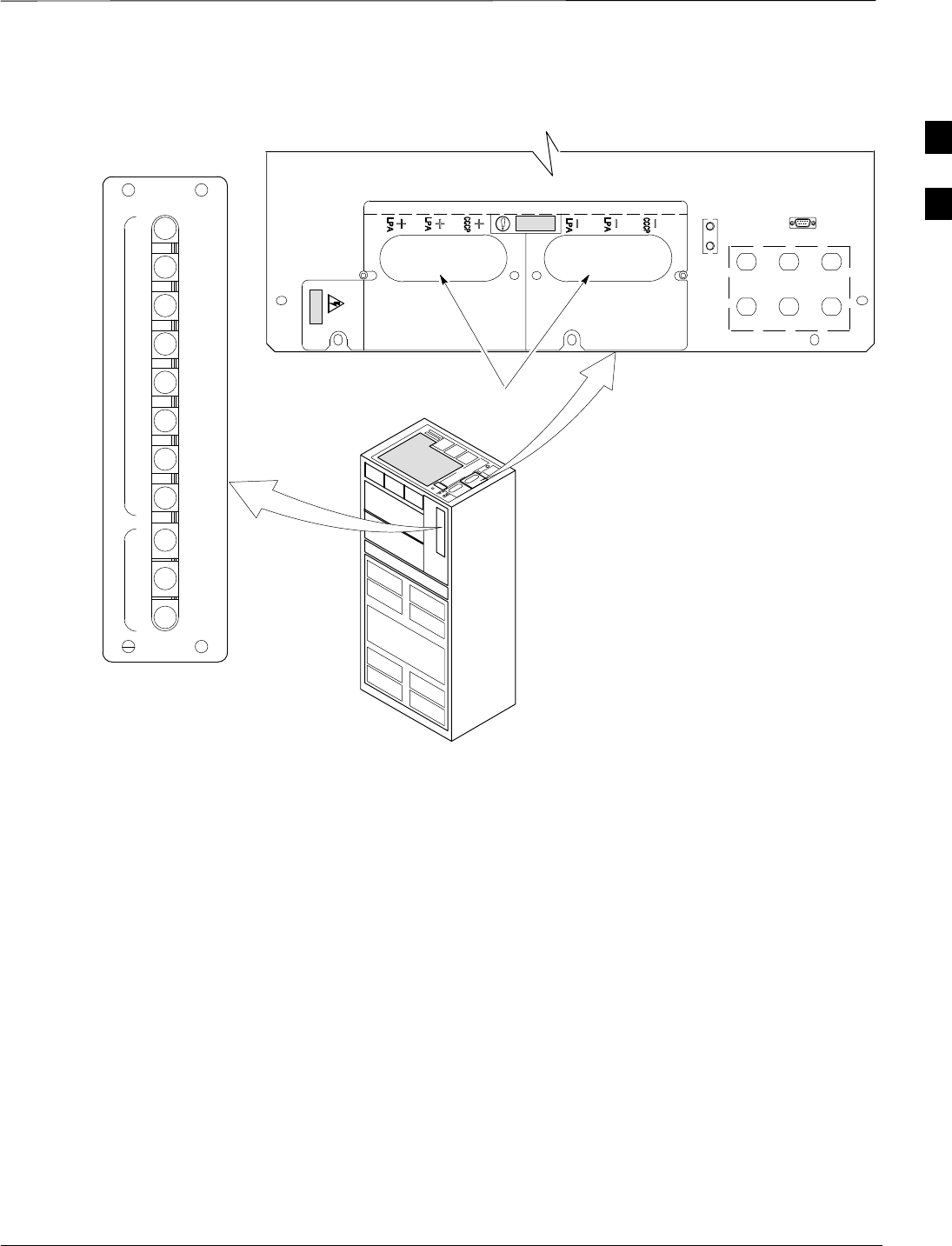
Frame Module Location & Identification – continued
Mar 2001 1-23
SCt4812T CDMA BTS Optimization/ATP DRAFT
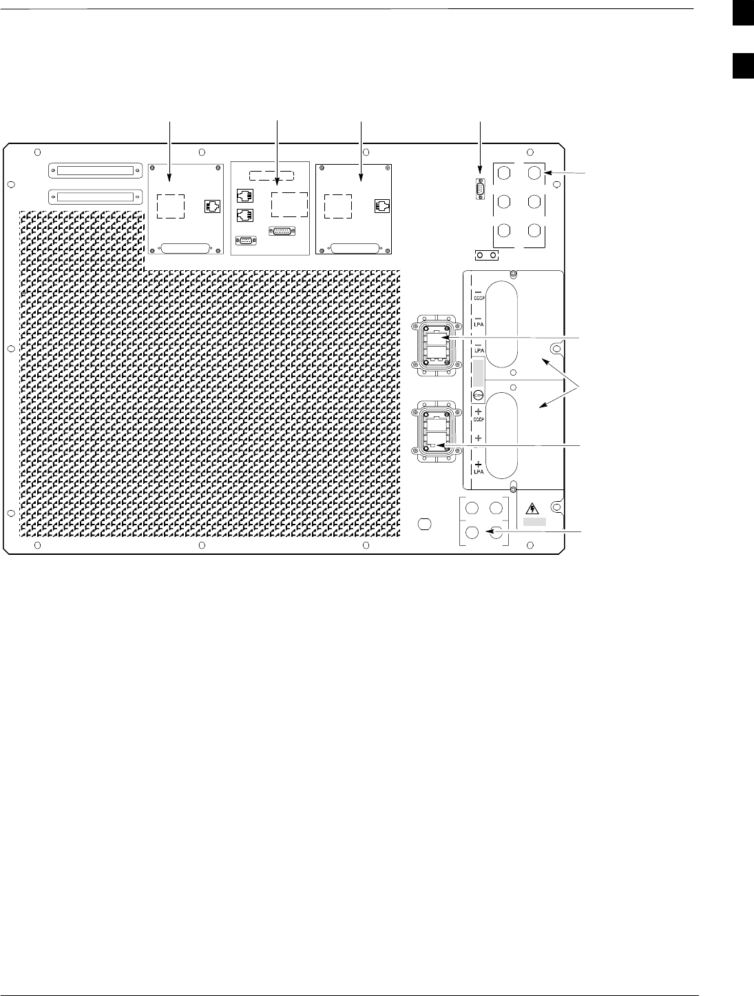
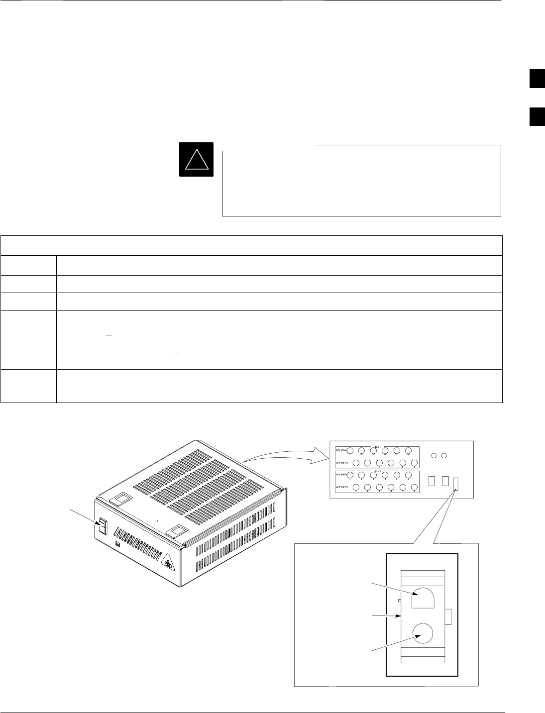
Figure 1-8: +27 V SC 4812T Expansion Frame I/O Plate
OUT
LAN
IN
LAN
AB
AB
GPS
EXP IN
SPAN I/O A SITE I/O SPAN I/O B
LFR/
ALARM B
4
GND
5
6
1
2
3
TX OUT
FRONT
REAR
SPAN I/O ASPAN I/O B
AB
CAUTION
LIVE TERMINALSLIVE TERMINALS +27 VDC
HSO
EXP OUT
AB
ALARM A
FW00082
EXP IN
HOUSING
TRANSMIT
ANTENNA
CONNECTORS
EXP OUT
HOUSING (ADDED
ONLY WHEN
USING SECOND
EXPANSION
FRAME)
SITE I/O LFR/HSO
RGD
POWER
INPUT
LAN
SPAN I/O SPAN I/O
RGPS
REF
1
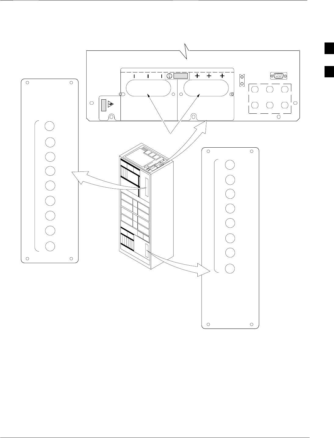
Frame Module Location & Identification – continued
DRAFT
SCt4812T CDMA BTS Optimization/ATP Mar 2001
1-24
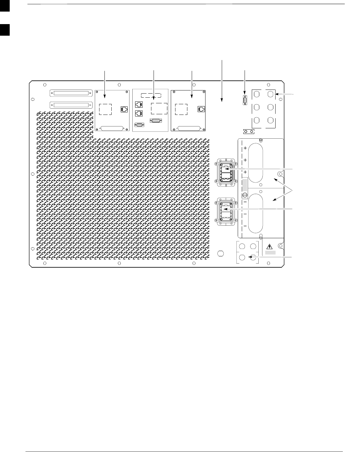
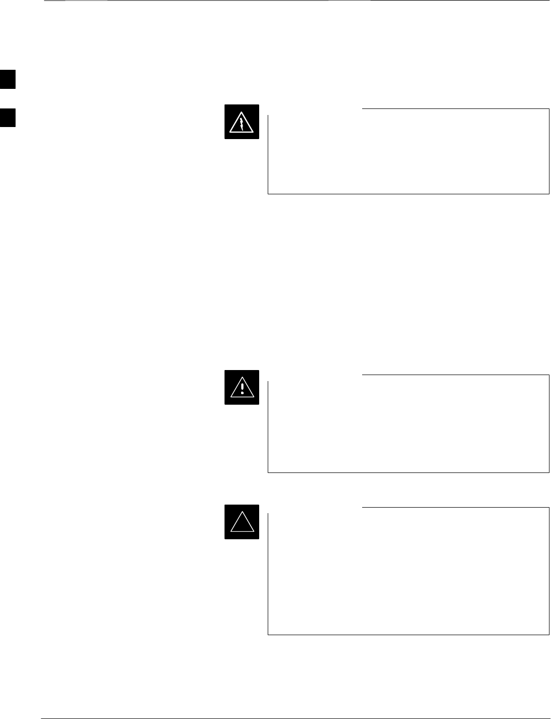
Figure 1-9: –48 V SC 4812T Expansion Frame I/O Plate
OUT
LAN
IN
LAN
AB
AB
GPS
EXP IN
SPAN I/O A SITE I/O SPAN I/O B
LFR
ALARM B
4
GND
5
6
1
2
3
TX OUT
FRONT
REAR
SPAN I/O ASPAN I/O B
AB
CAUTION
LIVE TERMINALS
HSO/
EXP OUT
AB
ALARM A
FW00480
EXP IN
HOUSING
TRANSMIT
ANTENNA
CONNECTORS
EXP OUT
HOUSING (ADDED
ONLY WHEN
USING SECOND
EXPANSION
FRAME)
SITE I/O
RGD
POWER
INPUT
LAN
SPAN I/O SPAN I/O
1
2
3
1
2
3
LIVE TERMINALS WIRED FOR –48 VDC
SITE I/O
HSO/LFR
RF FILTER PORTS NOT USED
IN EXPANSION FRAME
RGPS
REF
1
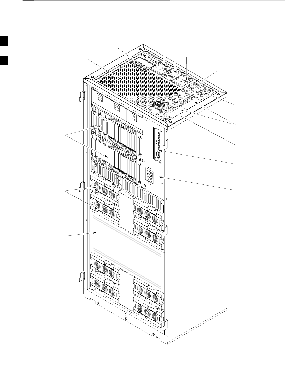
Frame Module Location & Identification – continued
Mar 2001 1-25
SCt4812T CDMA BTS Optimization/ATP DRAFT
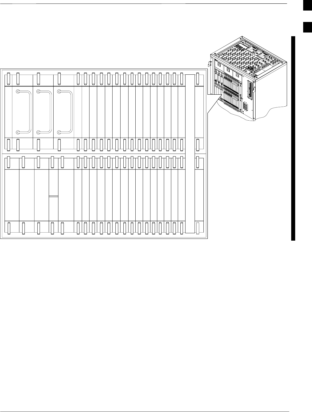
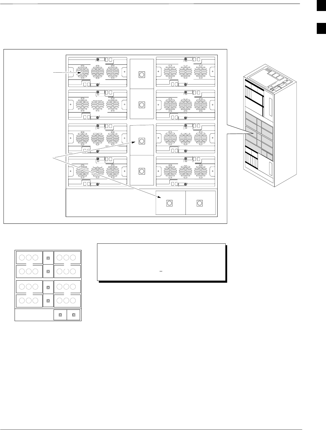
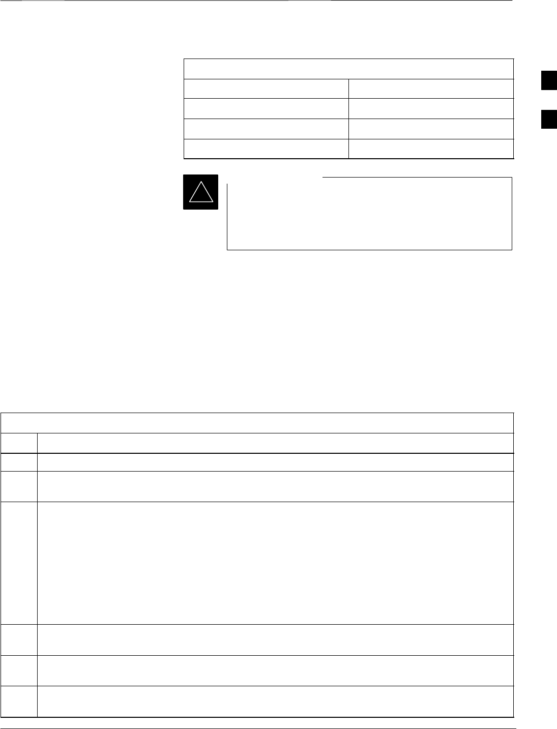
Figure 1-10: SC 4812T C–CCP Shelf
19 mm Filler Panel
PS–3
AMR–1
CSM–1
CSM–2
38 mm Filler Panel
AMR–2
GLI2–1GLI2–2
MCC24–6
BBX2–1
BBX2–2
BBX2–3
BBX2–4
BBX2–5
BBX2–6
BBX2–RSwitch
MPC/EMPC–1MPC/EMPC–2
CIO
BBX2–7
BBX2–8
BBX2–9
BBX2–10
BBX2–11
BBX2–12
MCC24–5
MCC24–4
MCC24–3
MCC24–2
MCC24–1
MCC24–12
MCC24–11
MCC24–10
MCC24–9
MCC24–8
MCC24–7
PS–2
PS–1
CCD–2 CCD–1
NOTE: MCCs may be
MCC8Es, MCC24s, or
MCC–1Xs. BBXs may
be BBX2s or BBX–1Xs.
HSO/LFR
FW00295
REF
1
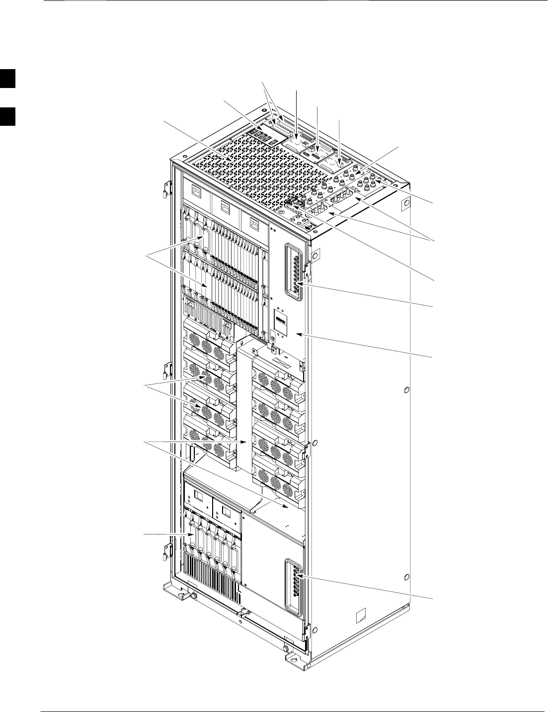
Frame Module Location & Identification – continued
DRAFT
SCt4812T CDMA BTS Optimization/ATP Mar 2001
1-26
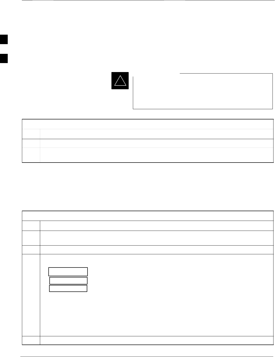
LPA1A
LPA1B
LPA1C
LPA1D
LPA3A
LPA3B
LPA3C
LPA3D
LPA2A
LPA2B
LPA2C
LPA2D
LPA4A
LPA4B
LPA4C
LPA4D
FAN
MODULE
(TYPICAL)
FILTERS /
COMBINERS
(2 TO 1 COMBINER
SHOWN)
Note
No adjacent carriers may exist within the same TX filter
combiner. “Adjacent” is defined as fc1 and fc2 being
1.25 MHz apart (center–to–center). “Non–adjacent” is
defined as fc1 and fc2 being >2.50 MHz apart
(center–to–center).
123
456
4–CARRIER CONFIGURATION
CARRIER
1
3
CARRIER
2
4
123
456
FW00296
Figure 1-11: +27 V SC 4812T LPA Configuration – 4 Carrier with 2:1 Combiners
1
Frame Module Location & Identification – continued
Mar 2001 1-27
SCt4812T CDMA BTS Optimization/ATP DRAFT
Figure 1-12: –48 V SC 4812T LPA Configuration – 4 Carrier, 3–Sector with 2:1 Combiners
LPA1A
LPA1B
Note
No adjacent carriers may exist within the same TX filter
combiner. “Adjacent” is defined as fc1 and fc2 being
1.25 MHz apart (center–to–center). “Non–adjacent” is
defined as fc1 and fc2 being >2.50 MHz apart
(center–to–center).
4–CARRIER CONFIGURATION
CARRIER CARRIER
LPA1C
LPA1D
LPA3C
LPA3D
LPA2A
LPA2B
LPA2C
LPA2D
LPA4C
LPA4D
FW00481
1
2
3
4
5
6
12
3 4
1
2
3
4
5
6
LPA3A
LPA3B
LPA4A
LPA4B
FAN
MODULE
(TYPICAL)
FILTERS /
COMBINERS
(2 TO 1 COMBINER
SHOWN)
–48 Volt
SC 4812T
1
Frame Module Location & Identification – continued
DRAFT
SCt4812T CDMA BTS Optimization/ATP Mar 2001
1-28
Sector Configuration
There are a number of ways to configure the BTS frame. Table 1-3
outlines the basic requirements. When carrier capacity is greater than
two, a 2:1 or 4:1 cavity combiner must be used. For one or two carriers,
bandpass filters or cavity combiners may be used, depending on
sectorization and channel sequencing.
Table 1-3: BTS Sector Configuration
Number
of carriers Number
of sectors Channel
spacing Filter requirements
13 or 6 N/A Bandpass Filter, Cavity Combiner
(2:1 or 4:1)
2 6 Non–adjacent Cavity Combiner (2:1 Only)
2 6 Adjacent Not supported in single frame
2 3 Non–adjacent Cavity Combiner (2:1 or 4:1)
2 3 Adjacent Bandpass Filter
3,4 3 Non–adjacent Cavity Combiner (2:1 or 4:1)
3,4 3 Adjacent Cavity Combiner (2:1 Only)
In Table 1-4, BBXs may be BBX2s or BBX–1Xs.
NOTE
1
Frame Module Location & Identification – continued
Mar 2001 1-29
SCt4812T CDMA BTS Optimization/ATP DRAFT
Table 1-4: Sector Configurations
Config Ref. No. Description
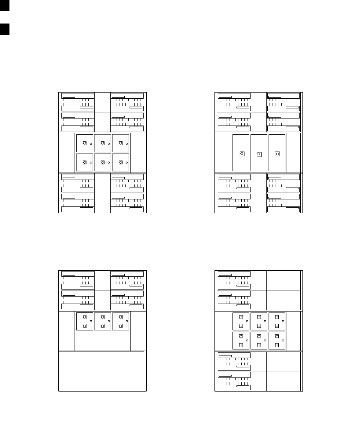
3–Sector/2–ADJACENT Carriers – The configuration below maps TX with optional 2:1 cavity
combiners for 3 sectors/2 carriers for adjacent channels. Note that 2:1 cavity combiners are used (6
total).
1TX1 TX2 TX3 TX4 TX5 TX6 Carrier#
BBX–1 BBX–2 BBX–3 N/A N/A N/A 1
N/A N/A N/A BBX–4 BBX–5 BBX–6 2
6–Sector/2–NON–ADJACENT Carriers – The configuration below maps TX with 2:1 cavity
combiners for 6 sectors/2 carriers for non–adjacent channels.
2TX1 TX2 TX3 TX4 TX5 TX6 Carrier#
BBX–1 BBX–2 BBX–3 BBX–4 BBX–5 BBX–6 1
BBX–7 BBX–8 BBX–9 BBX–10 BBX–11 BBX–12 2
3–Sector/2–NON–ADJACENT Carriers – The configuration below maps TX with 2:1 cavity
combiners for 3 sectors/2 carriers for non–adjacent channels.
3TX1 TX2 TX3 TX4 TX5 TX6 Carrier#
BBX–1 BBX–2 BBX–3 N/A N/A N/A 1
BBX–7 BBX–8 BBX–9 N/A N/A N/A 2
3–Sector/4–ADJACENT Carriers – The configuration below maps TX with 2:1 cavity combiners
for 3 sector/4 carriers for adjacent channels.
TX1 TX2 TX3 TX4 TX5 TX6 Carrier#
4BBX–1 BBX–2 BBX–3 N/A N/A N/A 1
BBX–7 BBX–8 BBX–9 N/A N/A N/A 2
N/A N/A N/A BBX–4 BBX–5 BBX–6 3
N/A N/A N/A BBX–10 BBX–11 BBX–12 4
3–Sector / 2–ADJACENT Carriers – The configuration below maps TX with bandpass filters for
3 sectors/2 carriers for adjacent channels.
5TX1 TX2 TX3 TX4 TX5 TX6 Carrier#
BBX–1 BBX–2 BBX–3 N/A N/A N/A 1
N/A N/A N/A BBX–7 BBX–8 BBX–9 2
3–Sector/3 or 4–NON–ADJACENT Carriers – The configuration below maps TX with 4:1
cavity combiners for 3 sectors/3 or 4 carriers for non–adjacent channels.
TX1 TX2 TX3 TX4 TX5 TX6 Carrier#
6BBX–1 BBX–2 BBX–3 N/A N/A N/A 1
BBX–7 BBX–8 BBX–9 N/A N/A N/A 2
BBX–4 BBX–5 BBX–6 N/A N/A N/A 3
BBX–10 BBX–11 BBX–12 N/A N/A N/A 4
6–Sector/1–Carrier – The configuration below maps TX with either bandpass filters or 2:1 cavity
combiners for 6 sector/1 carrier.
7TX1 TX2 TX3 TX4 TX5 TX6 Carrier#
BBX–1 BBX–2 BBX–3 BBX–4 BBX–5 BBX–6 1
1
Frame Module Location & Identification – continued
DRAFT
SCt4812T CDMA BTS Optimization/ATP Mar 2001
1-30
Numbering
456
LPA 1A
LPA 1B
LPA 1C
LPA 1D
LPA 3C
LPA 3A
LPA 3B
LPA 3D
LPA 2D
LPA 2C
LPA 2B
LPA 2A
LPA 4B
LPA 4A
LPA 4C
LPA 4D
Sector
3 Sector
Sector
3 Sector
(6 Sector)
Numbering
2 to 1 Combiner
3 Sector or 6 Sector
C1, S1–3
(C1, S1–3) C2, S1–3
(C2, S1–3)
C3, S1–3
(C1, S4–6) C4, S1–3
(C2, S4–6)
(6 Sector)
123
456
LPA 1A
LPA 1B
LPA 1C
LPA 1D
LPA 3C
LPA 3A
LPA 3B
LPA 3D
LPA 2D
LPA 2C
LPA 2B
LPA 2A
LPA 4B
LPA 4A
LPA 4C
LPA 4D
Sector
Numbering Sector
Numbering
4 to 1 Combiner
3 Sector
C1, S1–3 C2, S1–3
C3, S1–3 C4, S1–3
123
LPA 1A
LPA 1B
LPA 1C
LPA 1D LPA 2D
LPA 2C
LPA 2B
LPA 2A
Sector
3 Sector
Numbering Sector
3 Sector
Numbering
Dual Bandpass Filter
3 Sector Only
C1, S1–3 C2, S1–3
123
456
LPA 1A
LPA 1B
LPA 1C
LPA 1D
LPA 3C
LPA 3A
LPA 3B
LPA 3D
Sector
Numbering Dual Bandpass Filter
6 Sector
C1, S1–3
C1, S4–6
2 Carrier Maximum 1 Carrier Only
6 Sector
123
Figure 1-13: +27 V SC4812T LPA Configuration with Combiners/Filters
Note: See Table 1-4 Configuration
Reference Numbers 1, 2, 3, 4. Note: See Table 1-4 Configuration
Reference Number 6.
Note: See Table 1-4 Configuration
Reference Number 5. Note: See Table 1-4 Configuration
Reference Number 7.
FW00297
1
Frame Module Location & Identification – continued
Mar 2001 1-31
SCt4812T CDMA BTS Optimization/ATP DRAFT
Figure 1-14: –48 V SC4812T LPA Configuration with Combiners/Filters
Note: See Table 1-4 Configuration
Reference Numbers 1, 2, 3, 4. Note: See Table 1-4 Configuration
Reference Number 6.
Note: See Table 1-4 Configuration
Reference Number 5. Note: See Table 1-4 Configuration
Reference Number 7.
REF FW00482
4
1
5
2
36
Numbering
Sector
3 Sector
Sector
3 Sector
(6 Sector)
Numbering
2 to 1 Combiner
3 Sector or 6 Sector
C1, S1–3
(C1, S1–3) C2, S1–3
(C2, S1–3)
C3, S1–3
(C1, S4–6) C4, S1–3
(C2, S4–6)
(6 Sector)
LPA 1A
LPA 1B
LPA 1C
LPA 1D
LPA 3C
LPA 3A
LPA 3B
LPA 3D
LPA 2D
LPA 2C
LPA 2B
LPA 2A
LPA 4B
LPA 4A
LPA 4C
LPA 4D
Sector
Numbering Sector
Numbering
4 to 1 Combiner
3 Sector
C1, S1–3 C2, S1–3
C3, S1–3 C4, S1–3
LPA 1A
LPA 1B 1
3
LPA 1C
LPA 1D
LPA 3C
LPA 3A
LPA 3B
LPA 3D
LPA 2D
LPA 2C
LPA 2B
LPA 2A
LPA 4B
LPA 4A
LPA 4C
LPA 4D
2
LPA 1A
LPA 1B
LPA 1C
LPA 1D LPA 2D
LPA 2C
LPA 2B
LPA 2A
4
5
Sector
3 Sector
Numbering Sector
3 Sector
Numbering
Dual Bandpass Filter
3 Sector Only
C1, S1–3 C2, S1–3
2 Carrier Maximum
2
1
3
6
1
5
2
4
LPA 1A
LPA 1B
LPA 1C
LPA 1D
LPA 3C
LPA 3A
LPA 3B
LPA 3D
Sector
Numbering
Dual Bandpass Filter
6 Sector
C1, S1–3
C1, S4–6
1 Carrier Only
6 Sector
3 Sector
3 Sector
36
1
Frame Module Location & Identification – continued
DRAFT
SCt4812T CDMA BTS Optimization/ATP Mar 2001
1-32
Figure 1-15: –48 V BTS Power Conversion Shelf
FW00501
PS–6
AMR
PS–5
PS–4
PS–9
PS–8
PS–7
1C
1A
2A
2C
3C
3A
4A
4C
L
P
A
1D
1B
2B
2D
3D
3B
4B
4D
30
30
30
30
30
30
30
30
FAN
MODULE
PWR/ALM
REAR
FRONT
FAN
MODULE
PWR/ALM
REAR
FRONT
1
Frame Module Location & Identification – continued
Mar 2001 1-33
SCt4812T CDMA BTS Optimization/ATP DRAFT
Figure 1-16: CDMA (COBRA) RFDS Layout
AMR–B
(RS–485 SERIAL)
AMR–A
(RS–485 SERIAL)
Cobra RFDS external housing
(Shown With Cover off)
POWER SUPPLY
ON/OFF ROCKER
SWITCH
MMI PORT AND
PWR/ALARM LED
Cobra RFDS Field Replaceable Unit (FRU)
(shown removed from external housing)
CHASSIS GND
POWER
CONNECTOR
Cobra RFDS RF connector
panel detail
(shown from rear)
ELECTRICAL GND
FRONT VIEW
CASU 1
CASU 2
FWTIC
SUA ESN LABEL
(FOR SC XXXX SERIES BTS)
MMI
LEDS
ESN LABEL
(FOR SC 6XX SERIES BTS)
FW00138
1

Frame Module Location & Identification – continued
DRAFT
SCt4812T CDMA BTS Optimization/ATP Mar 2001
1-34
Notes
1

Mar 2001 SCt4812T CDMA BTS Optimization/ATP DRAFT
Chapter 2: Preliminary Operations
Table of Contents
Preliminary Operations: Overview 2-1. . . . . . . . . . . . . . . . . . . . . . . . . . . . . . . . . . .
Introduction 2-1. . . . . . . . . . . . . . . . . . . . . . . . . . . . . . . . . . . . . . . . . . . . . .
Cell Site Types 2-1. . . . . . . . . . . . . . . . . . . . . . . . . . . . . . . . . . . . . . . . . . . .
CDF 2-1. . . . . . . . . . . . . . . . . . . . . . . . . . . . . . . . . . . . . . . . . . . . . . . . . . . .
Site Equipage Verification 2-1. . . . . . . . . . . . . . . . . . . . . . . . . . . . . . . . . . .
Initial Installation of Boards/Modules 2-1. . . . . . . . . . . . . . . . . . . . . . . . . .
Setting Frame C–CCP Shelf Configuration Switch 2-3. . . . . . . . . . . . . . .
Pre–Power–up Tests 2-4. . . . . . . . . . . . . . . . . . . . . . . . . . . . . . . . . . . . . . . . . . . . . .
Objective 2-4. . . . . . . . . . . . . . . . . . . . . . . . . . . . . . . . . . . . . . . . . . . . . . . .
Test Equipment 2-4. . . . . . . . . . . . . . . . . . . . . . . . . . . . . . . . . . . . . . . . . . .
Cabling Inspection 2-4. . . . . . . . . . . . . . . . . . . . . . . . . . . . . . . . . . . . . . . . .
DC Power Pre-test (BTS Frame) 2-5. . . . . . . . . . . . . . . . . . . . . . . . . . . . . .
DC Power Pre-test (RFDS) 2-11. . . . . . . . . . . . . . . . . . . . . . . . . . . . . . . . . .
Initial Power–up Tests 2-12. . . . . . . . . . . . . . . . . . . . . . . . . . . . . . . . . . . . . . . . . . . .
Power-up Procedures 2-12. . . . . . . . . . . . . . . . . . . . . . . . . . . . . . . . . . . . . . .
Common Power Supply Verification 2-13. . . . . . . . . . . . . . . . . . . . . . . . . . .
Initial Power-up (RFDS) 2-14. . . . . . . . . . . . . . . . . . . . . . . . . . . . . . . . . . . .
Initial Power-up (BTS) 2-14. . . . . . . . . . . . . . . . . . . . . . . . . . . . . . . . . . . . .
2

Table of Contents – continued
DRAFT
SCt4812T CDMA BTS Optimization/ATP Mar 2001
Notes
2
Preliminary Operations: Overview
Mar 2001 2-1
SCt4812T CDMA BTS Optimization/ATP DRAFT
Introduction
This section first verifies proper frame equipage. This includes verifying
module placement, jumper, and dual in–line package (DIP) switch
settings against the site-specific documentation supplied for each BTS
application. Next, pre-power up and initial power-up procedures are
presented.
Cell Site Types
Sites are configured as Omni with a maximum of 4 carriers, 3–sectored
with a maximum of 4 carriers, and 6–sectored with a maximum of 2
carriers. Each type has unique characteristics and must be optimized
accordingly. For more information on the differences in site types, please
refer to the BTS/Modem Frame Hardware Installation manual.
CDF
The Cell-site Data File (CDF) contains site type and equipage data
information and passes it directly to the LMF during optimization. The
number of modem frames, C–CCP shelves, BBX boards, MCC boards
(per cage), and linear power amplifier assignments are some of the
equipage data included in the CDF.
Be sure that the correct bts–#.cdf and cbsc–#.cdf files are
used for the BTS. These should be the CDF files that are
provided for the BTS by the CBSC. Failure to use the
correct CDF files can cause system errors. Failure to use
the correct CDF files to log into a live (traffic carrying)
site can shut down the site.
IMPORTANT
*
Site Equipage Verification
Review the site documentation. Match the site engineering equipage data
to the actual boards and modules shipped to the site. Physically inspect
and verify the equipment provided for the BTS or Modem frame and
ancillary equipment frame.
Always wear a conductive, high impedance wrist strap
while handling any circuit card/module to prevent damage
by ESD. After removal, the card/module should be placed
on a conductive surface or back into the anti–static
shipping bag.
CAUTION
Initial Installation of
Boards/Modules
Follow the procedure in Table 2-1 to verify the initial installation of
boards/modules.
. . . continued on next page
2
Preliminary Operations: Overview – continued
DRAFT
SCt4812T CDMA BTS Optimization/ATP Mar 2001
2-2
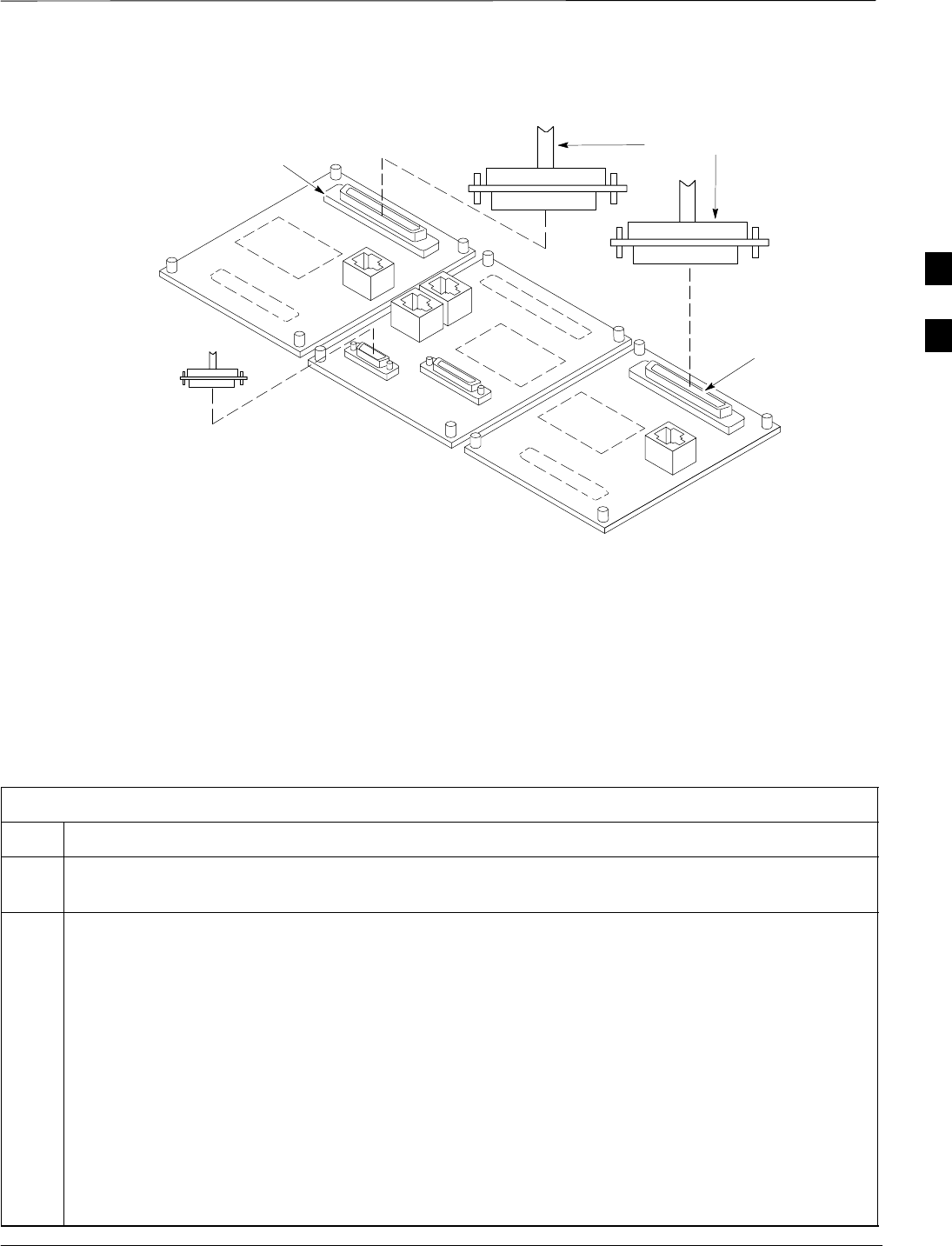
Table 2-1: Initial Installation of Boards/Modules
Step Action
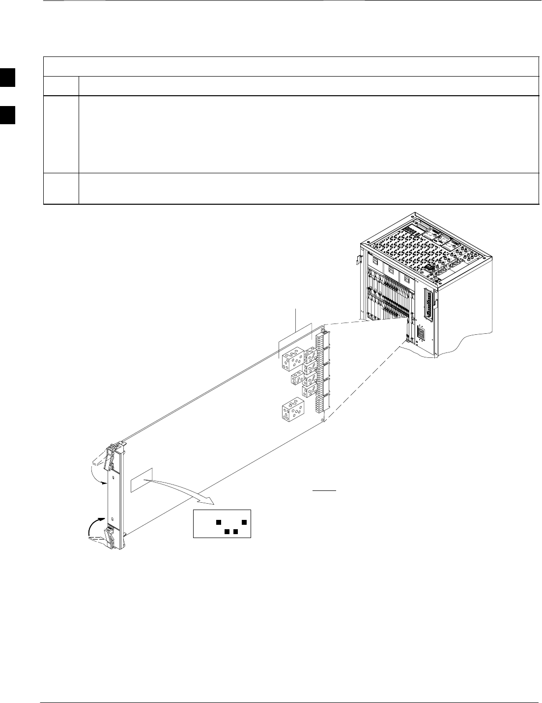
1Refer to the site documentation and install all boards and modules into the appropriate shelves as
required. Verify they are NOT SEATED at this time.
NOTE
On 800 MHz systems, the Switch Card has a configuration switch that must match the site
configuration (see Figure 2-1).
2As the actual site hardware is installed, record the serial number of each module on a “Serial Number
Checklist” in the site logbook.
Figure 2-1: Switch Card
Switch Card
1234
ON
BTS
MF
3 Sector
6 Sector
J1
J2
J3
J4
J5
SHIELDS
Configuration
Switch
NOTE:CONFIGURATION SWITCH ON
800 MHZ SWITCH CARD ONLY.
SHOWN FOR 3 SECTOR BTS.
SWITCH 1 CHOOSES BTS OR MF.
SWITCH 4 CHOOSES 3–SECTOR OR
6 SECTOR. SWITCHES 2 & 3 ARE NOT
USED.
FW00379
2
Preliminary Operations: Overview – continued
Mar 2001 2-3
SCt4812T CDMA BTS Optimization/ATP DRAFT
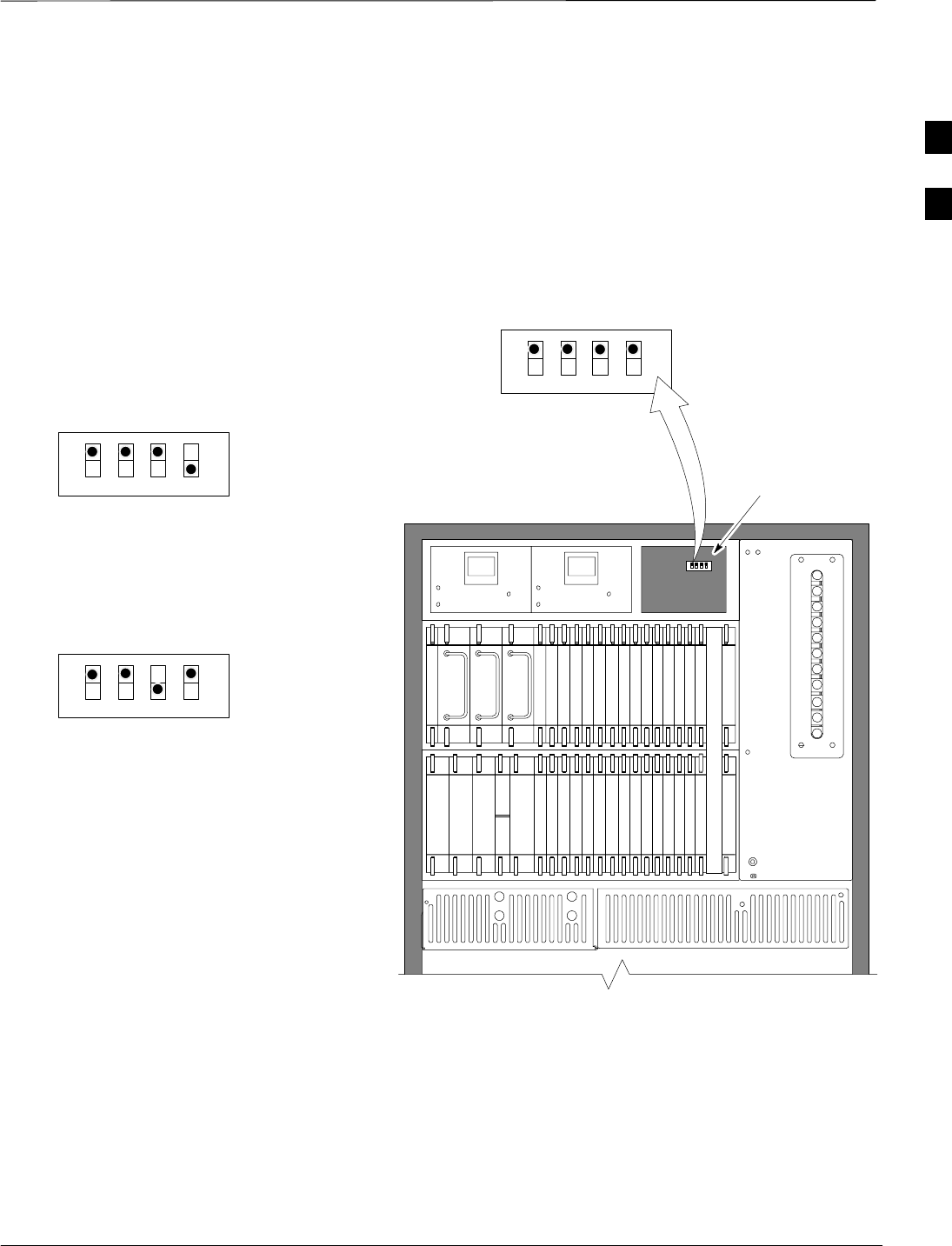
Setting Frame C–CCP Shelf
Configuration Switch
The backplane switch settings behind the fan module nearest the breaker
panel should be set as shown in Figure 2-2.
The switch setting must be verified and set before power is applied to the
BTS equipment.
Figure 2-2: Backplane DIP Switch Settings – SC 4812T
19 mm Filter Panel
Power Supply
AMR / MACH
HSO
CSM
CSM
39 mm Filter Panel
AMR / MACH
GLI2GLI2
MCC24–6
BBX2–1
BBX2–2
BBX2–3
BBX2–4
BBX2–5
BBX2–6
BBX2–R
Switch
MPCMPC
CIO
BBX2–7
BBX2–8
BBX2–9
BBX2–10
BBX2–11
BBX2–12
MCC24–5
MCC24–4
MCC24–3
MCC24–2
MCC24–1
MCC24–12
MCC24–11
MCC24–10
MCC24–9
MCC24–8
MCC24–7
Power Supply
Power Supply
CCD CCD
FAN
MODULE
PWR/ALM
REAR
FRONT
FAN
MODULE
PWR/ALM
REAR
FRONT
ON
OFF
SC 4812T C–CCP SHELF
FAN MODULE
REMOVED
STARTER
FRAME
SETTING
ON
OFF
EXPANSION
FRAME 1
SETTING
ON
OFF
EXPANSION
FRAME 2
SETTING
BOTTOM / TOP
RIGHT / LEFT
MODEM_FRAME_ID_1
MODEM_FRAME_ID_0
BOTTOM / TOP
RIGHT / LEFT
MODEM_FRAME_ID_1
MODEM_FRAME_ID_0
BOTTOM / TOP
RIGHT / LEFT
MODEM_FRAME_ID_1
MODEM_FRAME_ID_0
FW00151REF
2
Pre–Power–up Tests
DRAFT
SCt4812T CDMA BTS Optimization/ATP Mar 2001
2-4
Objective
This procedure checks for any electrical short circuits and verifies the
operation and tolerances of the cellsite and BTS power supply units prior
to applying power for the first time.
Test Equipment
The following test equipment is required to complete the pre–power–up
tests:
SDigital Multimeter (DMM)
Always wear a conductive, high impedance wrist strap
while handling the any circuit card/module to prevent
damage by ESD.
CAUTION
Cabling Inspection
Using the site-specific documentation generated by Motorola Systems
Engineering, verify that the following cable systems are properly
connected:
SReceive RF cabling – up to 12 RX cables
STransmit RF cabling – up to six TX cables
SGPS
SLFR
For positive power applications (+27 V):
SThe positive power cable is red.
SThe negative power cable (ground) is black.
For negative power applications (–48 V):
SThe negative power cable is red or blue.
SThe positive power cable (ground) is black.
In all cases, the black power cable is at ground potential.
IMPORTANT
*
2

Pre–Power–up Tests – continued
Mar 2001 2-5
SCt4812T CDMA BTS Optimization/ATP DRAFT
DC Power Pre-test (BTS Frame) Before applying any power to the BTS frame, follow the procedure in
Table 2-2 while referring to Figure 2-3 and Figure 2-4 for +27 V
systems or to Figure 2-5 and Figure 2-6 for –48 V systems to verify
there are no shorts in the BTS frame DC distribution system.
Table 2-2: DC Power Pre–test (BTS Frame)
Step Action
1Physically verify that all DC power sources supplying power to the frame are OFF or disabled.
2On each frame:
SUnseat all circuit boards (except CCD and CIO cards) in the C–CCP shelf and LPA shelves, but
leave them in their associated slots.
SSet C–CCP shelf breakers to the OFF position by pulling out power distribution breakers (labeled
C–CCP 1, 2, 3 on the +27 V BTS C–CCP power distribution panel and labeled POWER
1,4,5,2,6,7,3,8,9 on the –48 V C–CCP power distribution panel).
SSet LPA breakers to the OFF position by pulling out the LPA breakers (8 breakers, labeled 1A–1B
through 4C–4D – located on the C–CCP power distribution panel in the +27 V BTS or on the
power conversion shelf power distribution panel in the –48 V BTS).
3Verify that the resistance from the power (+ or –) feed terminals with respect to the ground terminal on
the top of the frame measures > 500 Ω (see Figure 2-3).
SIf reading is < 500 Ω, a short may exist somewhere in the DC distribution path supplied by the
breaker. Isolate the problem before proceeding. A reading > 3 MΩ could indicate an open (or
missing) bleeder resistor (installed across the filter capacitors behind the breaker panel).
4Set the C–CCP (POWER) breakers to the ON position by pushing them IN one at a time. Repeat
Step 3 after turning on each breaker.
* IMPORTANT* IMPORTANT
If the ohmmeter stays at 0 Ω after inserting any board/module, a short probably exists in that
board/module. Replace the suspect board/module and repeat the test. If test still fails, isolate the
problem before proceeding.
5Insert and lock the DC/DC converter modules for the C–CCP shelf and into their associated slots one
at a time. Repeat Step 3 after inserting each module.
SA typical response is that the ohmmeter steadily climbs in resistance as capacitors charge, finally
indicating approximately 500 Ω.
! CAUTION
Verify the correct power/converter modules by observing the locking/retracting tabs appear as follows:
– (in +27 V BTS C–CCP shelf)
– (in –48 V BTS C–CCP shelf)
STPN4045A
PWR CONV CDMA RCVR
STPN4009
PWR CONV CDMA RCVR
6Insert and lock all remaining circuit boards and modules into their associated slots in the C–CCP shelf.
Repeat Step 3 after inserting and locking each board or module.
SA typical response is that the ohmmeter steadily climbs in resistance as capacitors charge, stopping
at approximately 500 Ω..
. . . continued on next page
2
Pre–Power–up Tests – continued
DRAFT
SCt4812T CDMA BTS Optimization/ATP Mar 2001
2-6
Table 2-2: DC Power Pre–test (BTS Frame)
Step Action
7Set the LPA breakers ON by pushing them IN one at a time.
Repeat Step 3 after turning on each breaker.
SA typical response is that the ohmmeter will steadily climb in resistance as capacitors charge,
stopping at approximately 500 Ω..
8In the –48 V BTS, insert and lock the DC/DC LPA converter modules into their associated slots one at
a time.
Repeat Step 3 after inserting each module.
SA typical response is that the ohmmeter steadily climbs in resistance as capacitors charge, finally
indicating approximately 500 Ω.
! CAUTION
Verify the correct power/converter modules by observing the locking/retracting tabs appear as follows:
– (in –48 V BTS power conversion shelf)
STPN4044A
PWR CONV LPA
9Seat all LPA and associated LPA fan modules into their associated slots in the shelves one at a time.
Repeat Step 3 after seating each LPA and associated LPA fan module.
SA typical response is that the ohmmeter will steadily climb in resistance as capacitors charge,
stopping at approximately 500 Ω..
2
Pre–Power–up Tests – continued
Mar 2001 2-7
SCt4812T CDMA BTS Optimization/ATP DRAFT
POWER INPUT
TOP OF FRAME
BREAKER PANEL
LPA
BREAKERS
C–CCP
BREAKERS
4
GND
5
6
1
2
3
TX OUT
CAUTION
LIVE TERMINALSLIVE TERMINALS +27 VDC
LFR/
HSO
Figure 2-3: +27 V BTS DC Distribution Pre-test
Breakering:
S Two LPAs on each trunking backplane breakered together
S Designed for peak LPA current of 15 amps (30 amp breakers)
S Unused TX paths do not need to be terminated
S Single feed for C–CCP
S Dual feed for LPA
FW00298
1D
1B
2B
2D
1C
1A
2A
2C
30
30
30
30
30
30
30
30
3D
3B
4B
4D
3C
3A
4A
4C
50
50
50
1
2
3
C
C
P
L
P
A
C
. . . continued on next page
2
Pre–Power–up Tests – continued
DRAFT
SCt4812T CDMA BTS Optimization/ATP Mar 2001
2-8
Figure 2-4: +27 V SC 4812T BTS Starter Frame
Expansion I/O
Housing
For clarity, doors are not shown. FW00214
Front Cosmetic
Panel
Power Input
Connection
TX Out (1 – 6)
Span I/O B
Span I/O A
Site I/O
RX In (1A – 6A
and 1B – 6B)
Exhaust Region
C–CCP Cage
Breakers
Combiner
Section
RGD (Needed for
Expansion only)
LPA Cage
2
Pre–Power–up Tests – continued
Mar 2001 2-9
SCt4812T CDMA BTS Optimization/ATP DRAFT
Figure 2-5: –48 V BTS DC Distribution Pre-test
4
1
5
2
7
6
3
8
P
9
O
W
E
R
30
40
40
30
40
40
30
40
40
POWER INPUT
TOP OF FRAME
C–CCP BREAKER
LPA
BREAKER
4
GND
5
6
1
2
3
TX OUT
CAUTION
LIVE TERMINALSLIVE TERMINALS WIRED FOR –48 VDC
LFR
HSO/
Breakering:
S Two LPAs on each trunking backplane breakered together
S Designed for peak LPA current of 15 amps (30 amp breakers)
S Unused TX paths do not need to be terminated
S Single feed for C–CCP
S Dual feed for LPA
FW00483
1
2
3
1
2
3
1C
1A
2A
2C
3C
3A
4A
4C
L
P
A
1D
1B
2B
2D
3D
3B
4B
4D
30
30
30
30
30
30
30
30
2
Pre–Power–up Tests – continued
DRAFT
SCt4812T CDMA BTS Optimization/ATP Mar 2001
2-10
Figure 2-6: –48 V SC 4812T BTS Starter Frame
FW00477
Expansion I/O
Housing
For clarity, doors are not shown.
Front Cosmetic
Panel
Power Input
Connection
TX Out (1 – 6)
Span I/O B
Span I/O A
Site I/O
RX In (1A – 6A
and 1B – 6B)
Exhaust Region
C–CCP Cage
Breakers
Combiner
Section
RGD (Needed for
Expansion only)
LPA Cage
Power
Conversion
Shelf
Breakers
Alarms
2
Pre–Power–up Tests – continued
Mar 2001 2-11
SCt4812T CDMA BTS Optimization/ATP DRAFT
DC Power Pre-test (RFDS)
Before applying power to the RFDS, follow the steps in Table 2-3, while
referring to Figure 2-7, to verify there are no shorts in the RFDS DC
distribution system, backplanes, or modules/boards. As of the date of
this publication, the RFDS is not used with the –48 V BTS.
Visual inspection of card placement and equipage for each
frame vs. site documentation must be completed, as
covered in Table 2-1, on page 2-2, before proceeding with
this test.
IMPORTANT
*
Table 2-3: DC Power Pre-test (RFDS)
Step Action
1Physically verify that all DC/DC converters supplying the RFDS are OFF or disabled.
2Set the input power rocker switch P1 to the OFF position (see Figure 2-7).
3Verify the initial resistance from the power (+ or –) feed terminal with respect to ground terminal
measures > 5 kΩ , then slowly begins to increase.
SIf the initial reading is < 5 kΩ and remains constant, a short exists somewhere in the DC
distribution path supplied by the breaker. Isolate the problem before proceeding.
4Set the input power rocker switch P1 to the ON position.
Repeat Step 3.
Figure 2-7: DC Distribution Pre-test (COBRA RFDS Detail)
NOTE:
Set the input power switch ON while measuring the
resistance from the DC power – with respect to the
power + terminal on the rear of the COBRA RFDS.
INPUT POWER
SWITCH (P1)
FRONT OF COBRA RFDS
(cut away view shown for clarity)
RFDS REAR
INTERCONNECT PANEL
“–” CONNECTOR
PIN
“+” CONNECTOR
PIN
CONNECTOR (MADE
UP OF A HOUSING
AND TWO PINS)
FW00139
2
Initial Power–up Tests
DRAFT
SCt4812T CDMA BTS Optimization/ATP Mar 2001
2-12
Power-up Procedures
Potentially lethal voltage and current levels are routed to
the BTS equipment. This test must be performed with a
second person present, acting in a safety role. Remove all
rings, jewelry, and wrist watches prior to beginning this
test.
WARNING
DC Input Power
In the tests to follow, power will first be verified at the input to each
BTS frame. After power is verified, cards and modules within the frame
itself will be powered up and verified one at a time.
Before applying any power, verify the correct power feed and return
cables are connected between the power supply breakers and the power
connectors at the top of each BTS frame. Verify correct cable position
referring to Figure 2-3 on page 2-7 for +27 V systems and Figure 2-5 on
page 2-9 for –48 V systems.
Always wear a conductive, high impedance wrist strap
while handling any circuit card/module to prevent damage
by ESD. Extreme care should be taken during the removal
and installation of any card/module. After removal, the
card/module should be placed on a conductive surface or
back into the anti–static bag in which it was shipped.
CAUTION
For positive power applications (+27 V):
SThe positive power cable is red.
SThe negative power cable (ground) is black.
For negative power applications (–48 V):
SThe negative power cable is red or blue.
SThe positive power cable (ground) is black.
In all cases, the black power cable is at ground potential.
IMPORTANT
*
Motorola recommends that the DC input power cable used to connect the
frame to the main DC power source conforms to the guidelines outlined
in Table 2-4.
. . . continued on next page
2
Initial Power–up Tests – continued
Mar 2001 2-13
SCt4812T CDMA BTS Optimization/ATP DRAFT
Table 2-4: DC Input Power Cable Guidelines
Maximum Cable Length Wire Size
30.38 m (100 ft) 107 mm2 (AWG #4/0)
54.864 m (180 ft) 185 mm2 (350 kcmil)
Greater that 54.864 m (180 ft) Not recommended
*If Anderson SB350 style power connectors are used, make
sure the connector adapters are securely attached to each of
the BTS power feeds and returns. Also, make sure the
cables have been properly installed into each connector.
IMPORTANT
Common Power Supply
Verification
The procedure in Table 2-5 must be performed on any BTS frame
connected to a common power supply at the site after the common power
supply has been installed and verified per the power supply OEM
suggested procedures.
Perform the following steps to verify the power input is within
specification before powering up the individual cards/modules with the
frames themselves.
Table 2-5: Common Power Supply Verification
Step Action
1Physically verify that all DC power sources supplying the frame are OFF or disabled.
2On the RFDS (for +27 V systems only), set the input power switch P1 to the OFF position (see
Figure 2-7).
3On each frame:
SUnseat all circuit boards (except CCD and CIO cards) in the C–CCP shelf and LPA shelves, but
leave them in their associated slots.
SSet breakers to the OFF position by pulling out C–CCP and LPA breakers (see Figure 2-3 on
page 2-7 or Figure 2-5 on page 2-9 for breaker panel layout if required).
–C–CCP shelf breakers are labeled CCCP–1, 2, 3 in the +27 V BTS and labeled POWER
1,4,5,2,6,7,3,8,9 in the –48 V BTS.
–LPA breakers are labeled 1A–1B through 4C–4D.
4Inspect input cables, verify correct input power polarity via decal on top of frame (+27 Vdc or
–48 Vdc).
5Apply power to BTS frames, one at a time, by setting the appropriate breaker in the power supply that
supplies the frame to the ON position.
6After power is applied to each frame, use a digital voltmeter to verify power supply output voltages at
the top of each BTS frame are within specifications: +27.0 Vdc or –48 Vdc nominal.
2
Initial Power–up Tests – continued
DRAFT
SCt4812T CDMA BTS Optimization/ATP Mar 2001
2-14
Initial Power-up (RFDS)
The procedure in Table 2-6 must be performed on the RFDS after input
power from the common power supply has been verified. Perform the
following steps to apply initial power to the cards/modules within the
frame itself, verifying that each is operating within specification.
Visual inspection of card placement and equipage for each
frame vs. site documentation must be completed, as
covered in Table 2-1, on page 2-2, before proceeding with
this test.
IMPORTANT
*
Table 2-6: Initial Power-up (RFDS)
Step Action
1On the RFDS, set the input power rocker switch (P1) to the ON position (see Figure 2-7).
2Verify power supply output voltages (at the top of BTS frame), using a digital voltmeter, are within
specifications: +27.0 V nominal.
Initial Power-up (BTS)
The procedure must be performed on each frame after input power from
the common power supply has been verified. Follow the steps in
Table 2-7 to apply initial power to the cards/modules within the frame
itself, verifying that each is operating within specification.
Table 2-7: Initial Power–up (BTS)
Step Action
1At the BTS, set the C–CCP (POWER) power distribution breakers (see Figure 2-3 on page 2-7 or
Figure 2-5 on page 2-9) to the ON position by pushing in the breakers.
2Insert the C–CCP fan modules. Observe that the fan modules come on line.
3! CAUTION
Verify the correct power/converter modules by observing the locking/retracting tabs appear as follows:
–(in +27 V BTS C–CCP shelf)
–(in –48 V BTS C–CCP shelf)
–(in –48 V BTS power conversion shelf)
Insert and lock the converter/power supplies into their associated slots one at a time.
•If no boards have been inserted, all three PWR/ALM LEDs would indicate RED to notify the user
that there is no load on the power supplies.
–If the LED is RED, do not be alarmed. After Step 4 is performed, the LEDs should turn GREEN;
if not, then a faulty converter/power supply module is indicated and should be replaced before
proceeding.
STPN 4045A
PWR CONV CDMA RCVR
STPN 4044A
PWR CONV LPA
STPN4009
PWR CONV CDMA RCVR
4Seat and lock all remaining circuit cards and modules in the C–CCP shelf into their associated slots.
. . . continued on next page
2

Initial Power–up Tests – continued
Mar 2001 2-15
SCt4812T CDMA BTS Optimization/ATP DRAFT
Table 2-7: Initial Power–up (BTS)
Step Action
5Seat the first equipped LPA module pair into the assigned slot in the upper LPA shelf including LPA
fan.
SIn +27 V systems, observe that the LPA internal fan comes on line.
6Repeat step 5 for all remaining LPAs.
7Set the LPA breakers to the ON position (per configuration) by pushing them IN one at a time. See
Figure 1-13 on page 1-30 or Figure 1-14 on page 1-31 for configurations and Figure 2-3 on page 2-7
or Figure 2-5 on page 2-9 for LPA breaker panel layout.
On +27 V frames, engage (push) LPA circuit breakers.
SConfirm LEDs on LPAs light.
On –48 V frames, engage (push) LPA PS circuit breakers.
SConfirm LPA PS fans start.
SConfirm LEDs on –48 V power converter boards light.
SConfirm LPA fans start.
SConfirm LEDs on LPAs light.
8After all cards/modules have been seated and verified, use a digital voltmeter to verify power supply
output voltages at the top of the frame remain within specifications: +27.0 Vdc or –48 Vdc nominal.
9Repeat Steps 1 through 8 for additional co–located frames (if equipped).
2

Initial Power–up Tests – continued
DRAFT
SCt4812T CDMA BTS Optimization/ATP Mar 2001
2-16
Notes
2

Mar 2001 SCt4812T CDMA BTS Optimization/ATP DRAFT
Chapter 3: Optimization/Calibration
Table of Contents
Optimization/Calibration – Introduction 3-1. . . . . . . . . . . . . . . . . . . . . . . . . . . . . .
Introduction 3-1. . . . . . . . . . . . . . . . . . . . . . . . . . . . . . . . . . . . . . . . . . . . . .
Optimization Process 3-1. . . . . . . . . . . . . . . . . . . . . . . . . . . . . . . . . . . . . . .
Cell Site Types 3-2. . . . . . . . . . . . . . . . . . . . . . . . . . . . . . . . . . . . . . . . . . . .
Cell–Site Data File 3-2. . . . . . . . . . . . . . . . . . . . . . . . . . . . . . . . . . . . . . . . .
BTS System Software Download 3-3. . . . . . . . . . . . . . . . . . . . . . . . . . . . .
Site Equipage Verification 3-3. . . . . . . . . . . . . . . . . . . . . . . . . . . . . . . . . . .
Isolate Span Lines/Connect LMF 3-4. . . . . . . . . . . . . . . . . . . . . . . . . . . . . . . . . . . .
Isolate BTS from T1/E1 Spans 3-4. . . . . . . . . . . . . . . . . . . . . . . . . . . . . . .
LMF to BTS Connection 3-5. . . . . . . . . . . . . . . . . . . . . . . . . . . . . . . . . . . .
Preparing the LMF 3-7. . . . . . . . . . . . . . . . . . . . . . . . . . . . . . . . . . . . . . . . . . . . . . .
Overview 3-7. . . . . . . . . . . . . . . . . . . . . . . . . . . . . . . . . . . . . . . . . . . . . . . .
LMF Operating System Installation 3-7. . . . . . . . . . . . . . . . . . . . . . . . . . .
Copy CDF Files from CBSC 3-8. . . . . . . . . . . . . . . . . . . . . . . . . . . . . . . . .
Creating a Named HyperTerminal Connection for MMI Connection 3-10. .
Folder Structure Overview 3-13. . . . . . . . . . . . . . . . . . . . . . . . . . . . . . . . . . .
Pinging the Processors 3-14. . . . . . . . . . . . . . . . . . . . . . . . . . . . . . . . . . . . . .
Using CDMA LMF 3-18. . . . . . . . . . . . . . . . . . . . . . . . . . . . . . . . . . . . . . . . . . . . . .
Basic LMF Operation 3-18. . . . . . . . . . . . . . . . . . . . . . . . . . . . . . . . . . . . . .
Graphical User Interface Overview 3-18. . . . . . . . . . . . . . . . . . . . . . . . . . . .
Command Line Interface Overview 3-19. . . . . . . . . . . . . . . . . . . . . . . . . . . .
Logging into a BTS 3-20. . . . . . . . . . . . . . . . . . . . . . . . . . . . . . . . . . . . . . . .
Logging Out 3-22. . . . . . . . . . . . . . . . . . . . . . . . . . . . . . . . . . . . . . . . . . . . . .
Establishing an MMI Communication Session 3-24. . . . . . . . . . . . . . . . . . .
Download the BTS 3-25. . . . . . . . . . . . . . . . . . . . . . . . . . . . . . . . . . . . . . . . . . . . . . .
Download the BTS – Overview 3-25. . . . . . . . . . . . . . . . . . . . . . . . . . . . . . .
Download Code to Devices 3-26. . . . . . . . . . . . . . . . . . . . . . . . . . . . . . . . . .
Download Code and Data to Non–MGLI2 Devices 3-28. . . . . . . . . . . . . . .
Select CSM Clock Source 3-28. . . . . . . . . . . . . . . . . . . . . . . . . . . . . . . . . . .
Enable CSMs 3-29. . . . . . . . . . . . . . . . . . . . . . . . . . . . . . . . . . . . . . . . . . . . .
Enable MCCs 3-31. . . . . . . . . . . . . . . . . . . . . . . . . . . . . . . . . . . . . . . . . . . . .
Enable Redundant GLIs 3-31. . . . . . . . . . . . . . . . . . . . . . . . . . . . . . . . . . . . .
CSM System Time/GPS and LFR/HSO Verification 3-32. . . . . . . . . . . . . . . . . . . . .
CSM & LFR Background 3-32. . . . . . . . . . . . . . . . . . . . . . . . . . . . . . . . . . .
Low Frequency Receiver/High Stability Oscillator 3-33. . . . . . . . . . . . . . .
Front Panel LEDs 3-33. . . . . . . . . . . . . . . . . . . . . . . . . . . . . . . . . . . . . . . . .
3

Table of Contents – continued
DRAFT
SCt4812T CDMA BTS Optimization/ATP Mar 2001
Null Modem Cable 3-34. . . . . . . . . . . . . . . . . . . . . . . . . . . . . . . . . . . . . . . .
CSM Frequency Verification 3-34. . . . . . . . . . . . . . . . . . . . . . . . . . . . . . . . .
Test Equipment Setup: GPS & LFR/HSO Verification 3-34. . . . . . . . . . . . .
GPS Initialization/Verification 3-36. . . . . . . . . . . . . . . . . . . . . . . . . . . . . . . .
LFR Initialization/Verification 3-39. . . . . . . . . . . . . . . . . . . . . . . . . . . . . . . .
HSO Initialization/Verification 3-42. . . . . . . . . . . . . . . . . . . . . . . . . . . . . . .
Test Equipment Set–up 3-43. . . . . . . . . . . . . . . . . . . . . . . . . . . . . . . . . . . . . . . . . . . .
Connecting Test Equipment to the BTS 3-43. . . . . . . . . . . . . . . . . . . . . . . .
Supported Test Sets 3-43. . . . . . . . . . . . . . . . . . . . . . . . . . . . . . . . . . . . . . . .
Test Equipment Reference Chart 3-44. . . . . . . . . . . . . . . . . . . . . . . . . . . . . .
Equipment Warm-up 3-45. . . . . . . . . . . . . . . . . . . . . . . . . . . . . . . . . . . . . . .
Calibrating Cables 3-45. . . . . . . . . . . . . . . . . . . . . . . . . . . . . . . . . . . . . . . . .
Test Set Calibration 3-53. . . . . . . . . . . . . . . . . . . . . . . . . . . . . . . . . . . . . . . . . . . . . . .
Test Set Calibration Background 3-53. . . . . . . . . . . . . . . . . . . . . . . . . . . . . .
Purpose of Test set Calibration 3-53. . . . . . . . . . . . . . . . . . . . . . . . . . . . . . .
Selecting Test Equipment 3-54. . . . . . . . . . . . . . . . . . . . . . . . . . . . . . . . . . .
Manually Selecting Test Equipment in a Serial Connection Tab 3-54. . . . .
Automatically Selecting Test Equipment in a Serial Connection Tab 3-55. .
Calibrating Test Equipment 3-56. . . . . . . . . . . . . . . . . . . . . . . . . . . . . . . . . .
Calibrating Cables 3-56. . . . . . . . . . . . . . . . . . . . . . . . . . . . . . . . . . . . . . . . .
Calibrating Cables with a CDMA Analyzer 3-57. . . . . . . . . . . . . . . . . . . . .
Calibrating TX Cables Using a Signal Generator and
Spectrum Analyzer 3-58. . . . . . . . . . . . . . . . . . . . . . . . . . . . . . . . . . . . . . . .
Calibrating RX Cables Using a Signal Generator and
Spectrum Analyzer 3-59. . . . . . . . . . . . . . . . . . . . . . . . . . . . . . . . . . . . . . . .
Setting Cable Loss Values 3-61. . . . . . . . . . . . . . . . . . . . . . . . . . . . . . . . . . .
Setting TX Coupler Loss Value 3-62. . . . . . . . . . . . . . . . . . . . . . . . . . . . . . .
Bay Level Offset Calibration 3-63. . . . . . . . . . . . . . . . . . . . . . . . . . . . . . . . . . . . . . .
Introduction to Bay Level Offset Calibration 3-63. . . . . . . . . . . . . . . . . . . .
RF Path Bay Level Offset Calibration 3-63. . . . . . . . . . . . . . . . . . . . . . . . . .
When to Calibrate BLOs 3-63. . . . . . . . . . . . . . . . . . . . . . . . . . . . . . . . . . . .
TX Path Calibration 3-64. . . . . . . . . . . . . . . . . . . . . . . . . . . . . . . . . . . . . . . .
BLO Calibration Data File 3-65. . . . . . . . . . . . . . . . . . . . . . . . . . . . . . . . . .
Test Equipment Setup: RF Path Calibration 3-67. . . . . . . . . . . . . . . . . . . . .
TX Path Calibration 3-68. . . . . . . . . . . . . . . . . . . . . . . . . . . . . . . . . . . . . . . .
Download BLO Procedure 3-70. . . . . . . . . . . . . . . . . . . . . . . . . . . . . . . . . . .
Calibration Audit Introduction 3-70. . . . . . . . . . . . . . . . . . . . . . . . . . . . . . .
TX Path Audit 3-71. . . . . . . . . . . . . . . . . . . . . . . . . . . . . . . . . . . . . . . . . . . .
TX Audit Test 3-71. . . . . . . . . . . . . . . . . . . . . . . . . . . . . . . . . . . . . . . . . . . .
All Cal/Audit Test 3-72. . . . . . . . . . . . . . . . . . . . . . . . . . . . . . . . . . . . . . . . .
Create CAL File 3-74. . . . . . . . . . . . . . . . . . . . . . . . . . . . . . . . . . . . . . . . . . .
RFDS Setup and Calibration 3-75. . . . . . . . . . . . . . . . . . . . . . . . . . . . . . . . . . . . . . .
RFDS Description 3-75. . . . . . . . . . . . . . . . . . . . . . . . . . . . . . . . . . . . . . . . .
RFDS Parameter Settings 3-76. . . . . . . . . . . . . . . . . . . . . . . . . . . . . . . . . . .
RFDS TSU NAM Programming 3-78. . . . . . . . . . . . . . . . . . . . . . . . . . . . . .
Explanation of Parameters used when Programming the TSU NAM 3-78. .
Valid NAM Ranges 3-79. . . . . . . . . . . . . . . . . . . . . . . . . . . . . . . . . . . . . . . .
3

Table of Contents – continued
Mar 2001 SCt4812T CDMA BTS Optimization/ATP DRAFT
Set Antenna Map Data 3-80. . . . . . . . . . . . . . . . . . . . . . . . . . . . . . . . . . . . . .
Set RFDS Configuration Data 3-81. . . . . . . . . . . . . . . . . . . . . . . . . . . . . . . .
RFDS Calibration 3-82. . . . . . . . . . . . . . . . . . . . . . . . . . . . . . . . . . . . . . . . .
Program TSU NAM 3-83. . . . . . . . . . . . . . . . . . . . . . . . . . . . . . . . . . . . . . . .
BTS Redundancy/Alarm Testing 3-85. . . . . . . . . . . . . . . . . . . . . . . . . . . . . . . . . . . .
Objective 3-85. . . . . . . . . . . . . . . . . . . . . . . . . . . . . . . . . . . . . . . . . . . . . . . .
Test Equipment 3-85. . . . . . . . . . . . . . . . . . . . . . . . . . . . . . . . . . . . . . . . . . .
Redundancy/Alarm Test 3-85. . . . . . . . . . . . . . . . . . . . . . . . . . . . . . . . . . . .
Test Equipment Setup 3-86. . . . . . . . . . . . . . . . . . . . . . . . . . . . . . . . . . . . . .
Power Supply Redundancy 3-87. . . . . . . . . . . . . . . . . . . . . . . . . . . . . . . . . .
Miscellaneous Alarm/Redundancy Tests 3-89. . . . . . . . . . . . . . . . . . . . . . . .
BBX Redundancy 3-91. . . . . . . . . . . . . . . . . . . . . . . . . . . . . . . . . . . . . . . . .
CSM, GPS, & LFR/HSO Redundancy/Alarm Tests 3-92. . . . . . . . . . . . . . .
LPA Redundancy Test 3-95. . . . . . . . . . . . . . . . . . . . . . . . . . . . . . . . . . . . . .
MGLI/GLI Redundancy Test 3-96. . . . . . . . . . . . . . . . . . . . . . . . . . . . . . . . .
BTS Alarms Testing 3-97. . . . . . . . . . . . . . . . . . . . . . . . . . . . . . . . . . . . . . . . . . . . . .
Alarm Test Overview 3-97. . . . . . . . . . . . . . . . . . . . . . . . . . . . . . . . . . . . . . .
Alarm Reporting Display 3-97. . . . . . . . . . . . . . . . . . . . . . . . . . . . . . . . . . . .
Purpose 3-98. . . . . . . . . . . . . . . . . . . . . . . . . . . . . . . . . . . . . . . . . . . . . . . . .
Test Equipment 3-98. . . . . . . . . . . . . . . . . . . . . . . . . . . . . . . . . . . . . . . . . . .
CDI Alarm Input Verification with Alarms Test Box 3-99. . . . . . . . . . . . . .
CDI Alarm Input Verification without Alarms Test Box 3-102. . . . . . . . . . .
Pin and Signal Information for Alarm Connectors 3-103. . . . . . . . . . . . . . . .
3

Table of Contents – continued
DRAFT
SCt4812T CDMA BTS Optimization/ATP Mar 2001
Notes
3
Optimization/Calibration – Introduction
Mar 2001 3-1
SCt4812T CDMA BTS Optimization/ATP DRAFT
Introduction
This section describes procedures for isolating the BTS from the span
lines, preparing and using the LMF, downloading system operating
software, CSM reference verification/optimization, set up and calibration
of the supported test equipment, transmit/receive path verification, using
the RFDS, and verifying the customer defined alarms and relay contacts
are functioning properly.
Before using the LMF, use an editor to view the
”CAVEATS” section in the ”readme.txt” file in the c:\wlmf
folder for any applicable information.
IMPORTANT
*
Optimization Process
After a BTS is physically installed and the preliminary operations
(power up) have been completed, the LMF is used to calibrate and
optimize the BTS. Motorola recommends that the optimization be
accomplished as follows:
1. Download MGLI2–1 with code and data and then enable MGLI2–1.
2. Use the status function and verify that all of the installed devices of
the following types respond with status information: CSM, BBX,
GLI2, MCC, and TSU (if RFDS is installed). If a device is installed
and powered up but is not responding and is colored gray in the BTS
display, the device is not listed in the CDF file. The CDF file will
have to be corrected before the device can be accessed by the LMF.
3. Download code and data to all devices of the following types:
–CSM
–BBX (may be BBX2 or BBX–1X)
–GLI2 (other than MGLI2–1)
–MCC (may be MCC–8E, MCC24, or MCC–1X)
4. Download the RFDS TSIC (if installed).
5. Verify the operation of the GPS and HSO signals.
6. Enable the following devices (in the order listed):
–Secondary CSM
–Primary CSM
–All MCCs
7. Connect the required test equipment for a full optimization.
8. Select the test equipment.
9. Calibrate the TX and RX test cables if they have not previously been
calibrated using the CDMA LMF that is going to be used for the
optimization/calibration. The cable calibration values can also be
entered manually.
. . . continued on next page
3

Optimization/Calibration – Introduction – continued
DRAFT
SCt4812T CDMA BTS Optimization/ATP Mar 2001
3-2
10. Select all of the BBXs and all of the MCCs, and use the full
optimization function. The full optimization function performs TX
calibration, BLO download, TX audit, all TX tests, and all RX tests
for all selected devices.
11. If the TX calibration fails, repeat the full optimization for any failed
paths.
12. If the TX calibration fails again, correct the problem that caused the
failure and repeat the full optimization for the failed path.
13. If the TX calibration and audit portion of the full optimization passes
for a path but some of the TX or RX tests fail, correct the problem
that caused the failure and run the individual tests as required until
all TX and RX tests have passed for all paths.
Cell Site Types
Sites are configured as Omni/Omni or Sector/Sector (TX/RX). Each type
has unique characteristics and must be optimized accordingly.
For more information on the differences in site types,
please refer to the applicable BTS/Modem Frame Hardware
Installation and Functional Hardware Description
manuals.
NOTE
Cell–Site Data File
The Cell–SiteData File (CDF) contains information that defines the BTS
and data used to download files to the devices. A CDF file must be
placed in the applicable BTS folder before the LMF can be used to log
into that BTS. CDF files are normally obtained from the CBSC using a
floppy disk. A file transfer protocol (ftp) method can be used if the LMF
computer has that capability.
The CDF includes the following information:
SDownload instructions and protocol
SSite specific equipage information
SC–CCP shelf allocation plan
–BBX equipage (based on cell–site type) including redundancy
–CSM equipage including redundancy
–MCC (MCC24E, MCC8E, or MCC–1X) channel element allocation
plan. This plan indicates how the C–CCP shelf is configured, and
how the paging, synchronization, traffic, and access channel
elements (and associated gain values) are assigned among the (up to
12) MCCs in the shelf.
SCSM equipage including redundancy
. . . continued on next page
3
Optimization/Calibration – Introduction – continued
Mar 2001 3-3
SCt4812T CDMA BTS Optimization/ATP DRAFT
SEffective Rated Power (ERP) table for all TX channels to antennas
respectively. Motorola System Engineering specifies the ERP of a
transmit antenna based on site geography, antenna placement, and
government regulations. Working from this ERP requirement, the
antenna gain, (dependent on the units of measurement specified) and
antenna feed line loss can be combined to determine the required
power at the top of the BTS frame. The corresponding BBX output
level required to achieve that power level on any channel/sector can
also be determined.
Refer to the CDMA LMF Operator’s Guide, 68P64114A78,
for additional information on the layout of the LMF
directory structure (including CDF file locations and
formats).
NOTE
BTS System Software
Download
BTS system software must be successfully downloaded to the BTS
processor boards before optimization can be performed. BTS operating
code is loaded from the LMF computer terminal.
Before using the LMF for optimization/ATP, the correct
bts–#.cdf and cbsc–#.cdf files for the BTS must be
obtained from the CBSC and put in a bts–# folder in the
LMF. Failure to use the correct CDF files can cause wrong
results. Failure to use the correct CDF files to log into a
live (traffic carrying) site can shut down the site.
IMPORTANT
*
The CDF is normally obtained from the CBSC on a DOS formatted
diskette, or through a file transfer protocol (ftp) if the LMF computer has
ftp capability. Refer to the CDMA LMF Operator’s Guide, or the LMF
Help screen, for the procedure.
Site Equipage Verification
If you have not already done so, use an editor to view the CDF, and
review the site documentation. Verify the site engineering equipage data
in the CDF matches the actual site hardware using a CDF conversion
table.
Always wear a conductive, high impedance wrist strap
while handling any circuit card/module to prevent damage
by ESD. Extreme care should be taken during the removal
and installation of any card/module. After removal, the
card/module should be placed on a conductive surface or
back into the anti–static bag in which it was shipped.
CAUTION
3
Isolate Span Lines/Connect LMF
DRAFT
SCt4812T CDMA BTS Optimization/ATP Mar 2001
3-4
Isolate BTS from T1/E1 Spans
At active sites, the OMC/CBSC must disable the BTS and
place it out of service (OOS). DO NOT remove the 50–pin
TELCO cable connected to the BTS frame site I/O board
J1 connector until the OMC/CBSC has disabled the BTS!
IMPORTANT
*
Each frame is equipped with one Site I/O and two Span I/O boards. The
Span I/O J1 connector provides connection of 25 pairs of wire. A GLI2
card can support up to six spans. In the SC 4812T configuration, the odd
spans (1, 3, and 5) terminate on the Span ”A” I/O; and the even spans (2,
4, and 6) terminate on the Span ”B” I/O.
Before connecting the LMF to the frame LAN, the OMC/CBSC must
disable the BTS and place it OOS to allow the LMF to control the
CDMA BTS. This prevents the CBSC from inadvertently sending
control information to the CDMA BTS during LMF based tests. Refer to
Figure 3-1 and Figure 3-2 as required.
Table 3-1: T1/E1 Span Isolation
Step Action
1From the OMC/CBSC, disable the BTS and place it OOS. Refer to SC OMC–R/CBSC System
Operator Procedures.
–The T1/E1 span 50–pin TELCO cable connected to the BTS frame SPAN I/O board J1 connector
can be removed from both Span I/O boards, if equipped, to isolate the spans.
NOTE
If a third party is used for span connectivity, the third party must be informed before disconnecting the
span line.
* IMPORTANT
Verify that you remove the SPAN cable, not the “MODEM/TELCO” connector.
3
Isolate Span Lines/Connect LMF – continued
Mar 2001 3-5
SCt4812T CDMA BTS Optimization/ATP DRAFT
Figure 3-1: Span I/O Board T1 Span Isolation
50–PIN TELCO
CONNECTORS
REMOVED
SPAN A CONNECTOR
(TELCO) INTERFACE
TO SPAN LINES
SPAN B CONNECTOR
(TELCO) INTERFACE
TO SPAN LINES
TOP of Frame
(Site I/O and Span I/O boards)
RS–232 9–PIN SUB D
CONNECTOR SERIAL
PORT FOR EXTERNAL
DIAL UP MODEM
CONNECTION (IF USED)
FW00299
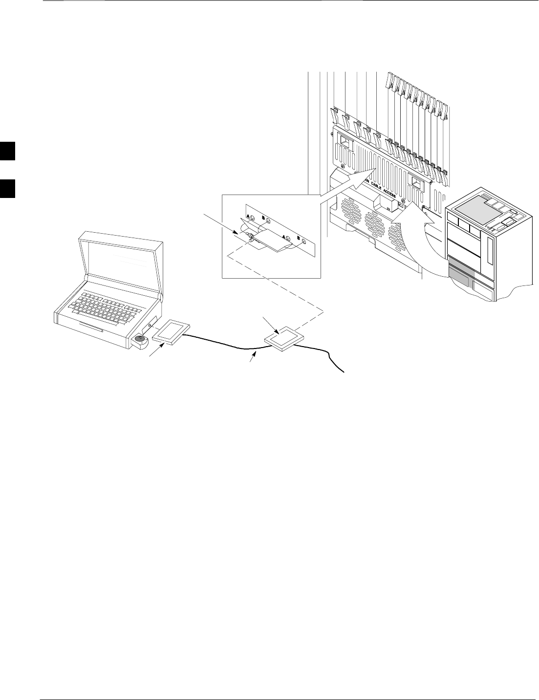
LMF to BTS Connection
The LMF is connected to the LAN A or B connector located on the left
side of the frame’s lower air intake grill, behind the LAN Cable Access
door (see Figure 3-2).
Table 3-2: LMF to BTS Connection
Step Action
1To gain access to the connectors on the BTS, open the LAN Cable Access door, then pull apart the
Velcro tape covering the BNC “T” connector (see Figure 3-2).
2Connect the LMF to the LAN A BNC connector via PCMCIA Ethernet Adapter with an unshielded
twisted–pair (UTP) Adapter and 10BaseT/10Base2 converter (powered by an external AC/DC
transformer).
–If there is no login response, connect the LMF to the LAN B connector.
–If there is still no login response, see Table 6-1, Login Failure Troubleshooting Procedures.
NOTE
–Xircom Model PE3–10B2 or equivalent can also be used to interface the LMF Ethernet
connection to the frame connected to the PC parallel port, powered by an external AC/DC
transformer. In this case, the BNC cable must not exceed 91 cm (3 ft) in length.
* IMPORTANT
–The LAN shield is isolated from chassis ground. The LAN shield (exposed portion of BNC
connector) must not touch the chassis during optimization.
3
Isolate Span Lines/Connect LMF – continued
DRAFT
SCt4812T CDMA BTS Optimization/ATP Mar 2001
3-6
Figure 3-2: LMF Connection Detail
NOTE:
Open LAN CABLE ACCESS
door. Pull apart Velcro tape and
gain access to the LAN A or LAN
B LMF BNC connector.
LMF BNC “T” CONNECTIONS
ON LEFT SIDE OF FRAME
(ETHERNET “A” SHOWN;
ETHERNET “B” COVERED
WITH VELCRO TAPE)
LMF COMPUTER
TERMINAL WITH
MOUSE PCMCIA ETHERNET
ADPATER & ETHERNET
UTP ADAPTER
10BASET/10BASE2
CONVERTER CONNECTS
DIRECTLY TO BNC T
115 VAC POWER
CONNECTION FW00140
UNIVERSAL TWISTED
PAIR (UTP) CABLE (RJ11
CONNECTORS)
3
Preparing the LMF
Mar 2001 3-7
SCt4812T CDMA BTS Optimization/ATP DRAFT
Overview
Software and files for installation and updating of the LMF are provided
on CD ROM disks. The following installation items must be available:
SLMF Program on CD ROM
SLMF Binaries on CD ROM
SCDF for each supported BTS (on diskette or available from the
CBSC)
SCBSC File for each supported BTS (on diskette or available from the
CBSC)
The following section provides information and instructions for
installing and updating the LMF software and files.
For the CDMA LMF graphics to display properly, the
computer platform must be configured to display more
than 256 colors. See the operating system software
instructions for verifying and configuring the display
settings.
IMPORTANT
*
LMF Operating System Installation
Follow the procedure in Table 3-3 to install the LMF operating system.
Table 3-3: LMF Operating System Installation
nStep Action
1Insert the LMF Program CD ROM into the LMF CD ROM drive.
–If the Setup screen is displayed, go to step 5.
–If the Setup screen is not displayed, proceed to step 2.
2Click on the Start button.
3 Select Run.
4In the Open box, enter d:\autorun and click on the OK button.
NOTE
If applicable, replace the letter d with the correct CD ROM drive letter.
. . . continued on next page
3

Preparing the LMF – continued
DRAFT
SCt4812T CDMA BTS Optimization/ATP Mar 2001
3-8
Table 3-3: LMF Operating System Installation
nActionStep
5Follow the instructions displayed on the Setup screen.
* IMPORTANT
First Time Installations:
–Install U/WIN (First)
–Install Java Runtime Environment (Second)
–Install LMF Software (Third)
–Install BTS Binaries (Fourth)
–Install/Create BTS Folders (Fifth)
Any time you install U/WIN, you must install the LMF software because the installation of the
LMF modifies some of the files that are installed during the U/Win installation. Installing U/Win
over–writes these modifications.
NOTE
There are multiple binary image packages for installation on the CD–ROM. When prompted,
choose the load that corresponds to the switch release that you currently have installed. Perform
the Device Images install after the WinLMF installation.
If applicable, a separate CD ROM of BTS Binaries may be available for binary updates.
Copy CDF Files from CBSC
Before the LMF can execute the optimization/ATP procedures for the
BTS, the correct bts-#.cdf and cbsc-#.cdf files must be
obtained from the CBSC and put in a bts-# folder in the LMF
notebook. This requires copying the CBSC CDF files to a DOS
formatted diskette, and using the diskette to install the CDF file in the
LMF.
Follow the procedure in Table 3-4 to obtain the CDF files from the
CBSC and copy the files to a diskette. For any further information, refer
to the CDMA LMF Operator’s Guide (Motorola part number
68P64114A78) or the LMF Help screen..
If the LMF has ftp capability, the ftp method can be used to
copy the CDF files from the CBSC.
On Sun OS workstations, the unix2dos command can be
used in place of the cp command (e.g., unix2dos
bts–248.cdf bts–248.cdf). This should be done using a
copy of the CBSC CDF file so the original CBSC CDF file
is not changed to DOS format.
NOTE
. . . continued on next page
3
Preparing the LMF – continued
Mar 2001 3-9
SCt4812T CDMA BTS Optimization/ATP DRAFT
*When copying CDF files, comply with the following to
prevent BTS login problems with the LMF:
– The numbers used in the bts–#.cdf and cbsc–#.cdf
filenames must correspond to the locally assigned numbers
for each BTS and its controlling CBSC.
– The generic cbsc–1.cdf file supplied with the LMF work
with locally numbered BTS CDF files. Using this file does
not provide a valid optimization unless the generic file is
edited to replace default parameters (e.g., channel numbers)
with the operational parameters used locally.
IMPORTANT
Table 3-4: Copying CBSC CDF Files to the LMF
nStep Action
AT THE CBSC:
1Login to the CBSC workstation.
2Insert a DOS formatted diskette in the workstation drive.
3 Type eject –q and press the <Enter> key.
4 Type mount and press the <Enter> key.
NOTE
SLook for the “floppy/no_name” message on the last line displayed.
SIf the eject command was previously entered, floppy/no_name will be appended with a
number. Use the explicit floppy/no_name reference displayed when performing step 7.
5Change to the directory containing the file by typing cd <directory name> (ex. cd
bts–248) and pressing <Enter>.
6 Type ls <Enter> to display the list of files in the directory.
7 With Solaris versions of Unix, create DOS–formatted versions of the bts–#.cdf and cbsc–#.cdf
files on the diskette by entering the following command:
unix2dos <source filename> /floppy/no_name/<target filename>
(e.g., unix2dos bts–248.cdf /floppy/no_name/bts–248.cdf).
NOTE
SOther versions of Unix do not support the unix2dos and dos2unix commands. In these cases,
use the Unix cp (copy) command. The copied files will be difficult to read with a DOS or
Windows text editor because Unix files do not contain line feed characters. Editing copied CDF
files on the LMF computer is, therefore, not recommended.
SUsing cp, multiple files can be copied in one operation by separating each filename to be copied
with a space and ensuring the destination directory (floppy/no_name) is listed at the end of the
command string following a space (e.g., cp bts–248.cdf cbsc–6.cdf /floppy/na_name).
. . . continued on next page
3
Preparing the LMF – continued
DRAFT
SCt4812T CDMA BTS Optimization/ATP Mar 2001
3-10
Table 3-4: Copying CBSC CDF Files to the LMF
nActionStep
8Repeat steps 5 through 7 for each bts–# that must be supported by the LMF.
9When all required files have been copied to the diskette, type eject and press the <Enter> key.
10 Remove the diskette from the CBSC.
AT THE LMF:
11 Start the Windows operating system.
12 Insert the diskette into the LMF.
13 Using Windows Explorer (or equivalent program), create a corresponding bts–# folder in the
wlmf\cdma directory for each bts–#.cdf/cbsc–#.cdf file pair copied from the CBSC.
14 Use Windows Explorer (or equivalent program) to transfer the cbsc–#.cdf and bts–#.cdf files from
the diskette to the corresponding wlmf\cdma\bts–# folders created in step 13.
Creating a Named
HyperTerminal Connection for
MMI Connection
Confirming or changing the configuration data of certain BTS Field
Replaceable Units (FRUs) requires establishing an MMI communication
session between the LMF and the FRU. Using features of the Windows
operating system, the connection properties for an MMI session can be
saved on the LMF computer as a named Windows HyperTerminal
connection. This eliminates the need for setting up connection
parameters each time an MMI session is required to support
optimization.
Once the named connection is saved, a shortcut for it can be created on
the Windows desktop. Double clicking the shortcut icon will start the
connection without the need to negotiate multiple menu levels.
Follow the procedure in Table 3-5 to establish a named HyperTerminal
connection and create a WIndows desktop shortcut for it.
There are differences between Windows NT and Windows
98 in the menus and screens for creating a HyperTerminal
connection. In the following procedure, items applicable
to:
– Windows NT will be identified with Win NT
– Windows 98 will be identified with Win 98
NOTE
. . . continued on next page
3

Preparing the LMF – continued
Mar 2001 3-11
SCt4812T CDMA BTS Optimization/ATP DRAFT
Table 3-5: Creating a Named Hyperlink Connection for MMI Connection
Step Action
1From the Windows Start menu, select:
Programs>Accessories
2Perform one of the following:
SFor Win NT, select Hyperterminal and then click on HyperTerminal
SFor Win 98, select Communications, double click the Hyperterminal folder, and then double click
on the Hyperterm.exe icon in the window that opens.
NOTE
SIf a Location Information Window appears, enter the required information, then click Close.
(This is required the first time, even if a modem is not to be used.)
SIf a You need to install a modem..... message appears, click NO.
3When the Connection Description box opens:
–Type a name for the connection being defined (e.g., MMI Session) in the Name: window.
–Highlight any icon preferred for the named connection in the Icon: chooser window.
–Click OK.
4
NOTE
For LMF configurations where COM1 is used by another interface such as test equipment and a
physical port is available for COM2, select COM2 to prevent conflicts.
From the Connect using: pick list in the Connect To box displayed, select the RS–232 port to be used
for the connection (e.g., COM1 or COM2 (Win NT) – or Direct to Com 1 or Direct to Com 2 (Win
98), and click OK.
5In the Port Settings tab of the COM# Properties window displayed, configure the RS–232 port
settings as follows:
SBits per second: 9600
SData bits: 8
SParity: None
SStop bits: 1
SFlow control: None
6 Click OK.
7Save the defined connection by selecting:
File>Save
8Close the HyperTerminal window by selecting:
File>Exit
9 Click Yes to disconnect when prompted.
. . . continued on next page
3

Preparing the LMF – continued
DRAFT
SCt4812T CDMA BTS Optimization/ATP Mar 2001
3-12
Table 3-5: Creating a Named Hyperlink Connection for MMI Connection
Step Action
10 Perform one of the following:
SIf the Hyperterminal folder window is still open (Win 98) proceed to step 12
SFrom the Windows Start menu, select Programs > Accessories
11 Perform one of the following:
SFor Win NT, select Hyperterminal and release any pressed mouse buttons.
SFor Win 98, select Communications and double click the Hyperterminal folder.
12 Highlight the newly created connection icon by moving the cursor over it (Win NT) or clicking on it
(Win 98).
13 Right click and drag the highlighted connection icon to the Windows desktop and release the right
mouse button.
14 From the pop–up menu displayed, select Create Shortcut(s) Here.
15 If desired, reposition the shortcut icon for the new connection by dragging it to another location on the
Windows desktop.
3

Preparing the LMF – continued
Mar 2001 3-13
SCt4812T CDMA BTS Optimization/ATP DRAFT
Folder Structure Overview
The LMF uses a wlmf folder that contains all of the essential data for
installing and maintaining the BTS. The list that follows outlines the
folder structure for the LMF. Except for the bts–nnn folders, these
folders are created as part of the the LMF installation. Refer to the
CDMA LMF Operator’s Guide for a complete description of the folder
structure.
Figure 3-3: LMF Folder Structure
version folder (A separate folder is
required for each different version; for
example, a folder name 2.8.1.1.1.5)
loads folder
(C:)
wlmf folder
cdma folder
code folder
data folder
BTS–nnn folders (A separate folder is
required for each BTS where bts–nnn is the
unique BTS number; for example, bts–163)
3
Preparing the LMF – continued
DRAFT
SCt4812T CDMA BTS Optimization/ATP Mar 2001
3-14
Pinging the Processors
For proper operation, the integrity of the Ethernet LAN A and B links
must be be verified. Figure 3-4 represents a typical BTS Ethernet
configuration. The drawing depicts one (of two identical) links, A and B.
Ping is a program that routes request packets to the LAN network
modules to obtain a response from the specified “targeted” BTS.
Figure 3-4: BTS LAN Interconnect Diagram
CHASSIS
GROUND
SIGNAL
GROUND
50Ω
SIGNAL
GROUND
50Ω
IN
LMF CONNECTOR
B
C–CCP
CAGE
AB
IN
A
B
A
OUT
OUT
BTS
(EXPANSION)
B
C–CCP
CAGE
AB
IN
A
B
A
OUT
BTS
(MASTER)
IN
OUT
FW00141
Follow the procedure in Table 3-6 and refer to Figure 3-5 or Figure 3-6,
as required, to ping each processor (on both LAN A and LAN B) and
verify LAN redundancy is operating correctly.
Always wear a conductive, high impedance wrist strap
while handling any circuit card/module to prevent damage
by ESD.
CAUTION
*The Ethernet LAN A and B cables must be installed on
each frame/enclosure before performing this test. All other
processor board LAN connections are made via the
backplanes.
IMPORTANT
. . . continued on next page
3

Preparing the LMF – continued
Mar 2001 3-15
SCt4812T CDMA BTS Optimization/ATP DRAFT
Table 3-6: Pinging the Processors
nStep Action
1If you have not already done so, connect the LMF to the BTS (see Table 3-2 on page 3-5).
2From the Windows desktop, click the Start button and select Run.
3In the Open box, type ping and the <MGLI IP address> (for example, ping 128.0.0.2).
NOTE
128.0.0.2 is the default IP address for MGLI–1 in field BTS units. 128.0.0.1 is the default IP address
for MGLI–2.
4Click on the OK button.
5If the connection is successful, text similar to the following is displayed:
Reply from 128 128.0.0.2: bytes=32 time=3ms TTL=255
If there is no response the following is displayed:
Request timed out
If the MGLI fails to respond, reset and perform the ping process again. If the MGLI still fails to
respond, typical problems are shorted BNC to inter-frame cabling, open cables, crossed A and B link
cables, missing 50–Ohm terminators, or the MGLI itself.
3
Preparing the LMF – continued
DRAFT
SCt4812T CDMA BTS Optimization/ATP Mar 2001
3-16
OUT
LAN
IN
LAN
GPS
AB
AB
SPAN I/O A SITE I/O SPAN I/O B
LFR/
ALARM B 4
3A
2A
1A
6A
5A
4A
3B
2B
1B
6B
5B
4B
GND
5
6
1
2
3
TX OUT
FRONT
REAR
ETHERNET CONNECTORS
WITH 50–OHM TERMINATORS
CAUTION
LIVE TERMINALSLIVE TERMINALS +27 VDC
HSO
Figure 3-5: +27 V SC 4812T Starter Frame I/O Plate
RX
ALARM A
FW00081
EXP I/O
RGD
TOP VIEW
RGPS
REF
3