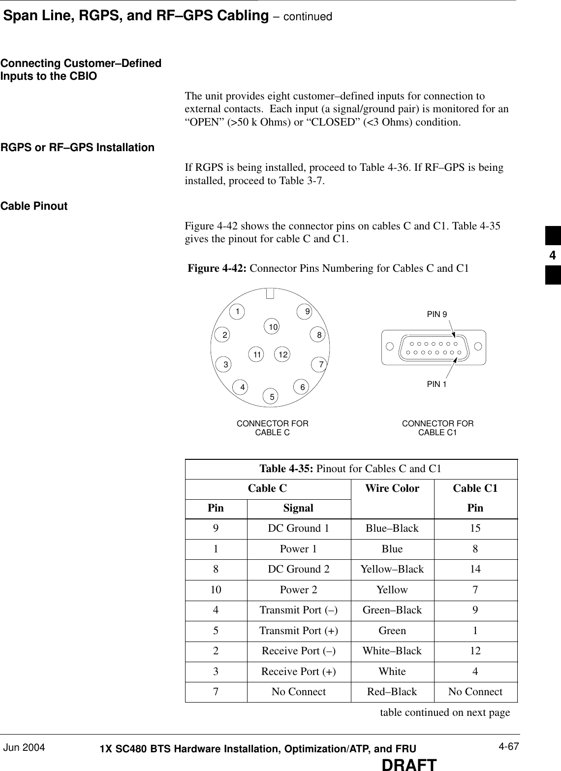
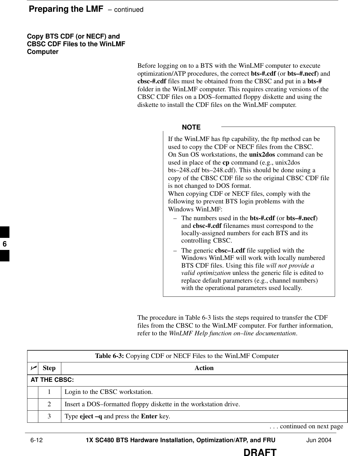
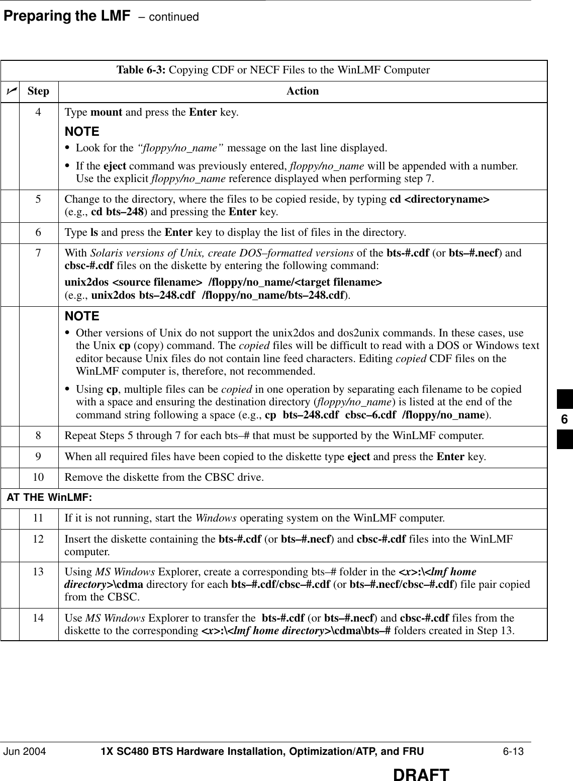
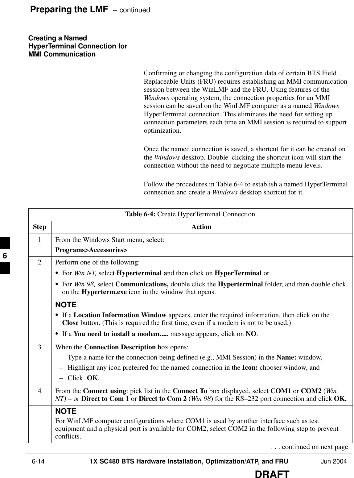
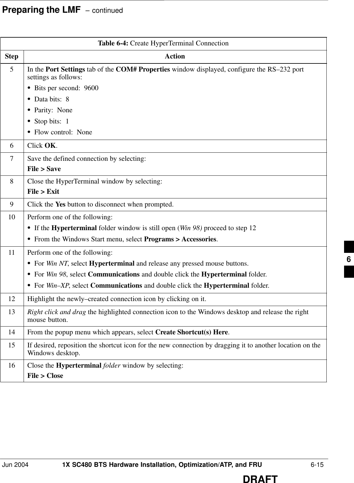
Nokia Solutions and Networks T6EK1 1X-EVDO SC480 BTS Microcell Base Station Transmtr User Manual print instructions
Nokia Solutions and Networks 1X-EVDO SC480 BTS Microcell Base Station Transmtr print instructions
Contents
- 1. User Manual Part 1 of 4
- 2. User Manual 2 of 4
- 3. User Manual 3 of 4
- 4. User Manual 4 of 4
User Manual 2 of 4
![Bay Level Offset Calibration – continued 6-80 1X SC480 BTS Hardware Installation, Optimization/ATP, and FRU Jun 2004DRAFTBLO Calibration Data FileDuring the calibration process, the LMF creates a calibration (CAL) datafile where BLO values are stored. After calibration has been completed,these offset values must be downloaded to the BBXs using the LMFBLO download function. A detailed description of the file organizationand content is provided in the following paragraphsNOTE Due to the size of the file, Motorola recommends printing out acopy of a bts–#.cal file and referring to it for the followingdescriptions.SWhen referring to the CAL file print–out it can be seen that there isone BBX slot with 20 “calibration entries” per BBX (sector) for eachbranch. Two calibration entries define a single “calibration point;”therefore there are ten calibration points in each branch for each BBX.– The first entry for a calibration point (all odd entries) identifies theCDMA channel (frequency) where the BLO is measured. Thesecond calibration entry (all even entries) is the power set level(PwrLvlAdj) for that frequency. The valid range for PwrLvlAdj isfrom 2500 to 27500 (2500 corresponds to –125 dBm and 27500corresponds to +125 dBm).– The ten calibration points for each slot–branch combination must bestored in order of increasing frequency. If less than ten points(frequencies) are calibrated, the BLO data for the highest frequencycalibrated is written into the remainder of the ten points for thatslot–branch.Example:C[1]=384 (odd cal entry)C[2]=19102 (even cal entry)C[3]=777 (odd cal entry)C[4]=19086 (even cal entry)C[19]=777 (odd cal entry)C[20]=19086 (even cal entry)...= 1 “calibration point”= 1 “calibration point”= 1 “calibration point”In the example above, BLO was measured at only two frequencies(channels 384 and 777) for CCP2 slot BBX–1 transmit. The BLO datafor the highest frequency measured (channel 777) will be written tothe remaining eight transmit calibration points (defined by entriesC[5] through C[20]) for BBX–1.Slot Block Temperature Compensation – Each BBX slot Block alsohas a temperature compensation data section (TempLevelCal) wherepower level compensation factors for temperature variations are stored.6](https://usermanual.wiki/Nokia-Solutions-and-Networks/T6EK1.User-Manual-2-of-4/User-Guide-448329-Page-116.png)
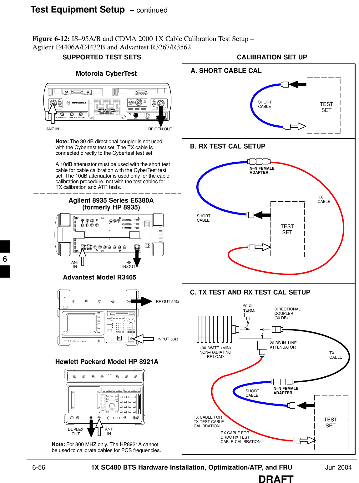
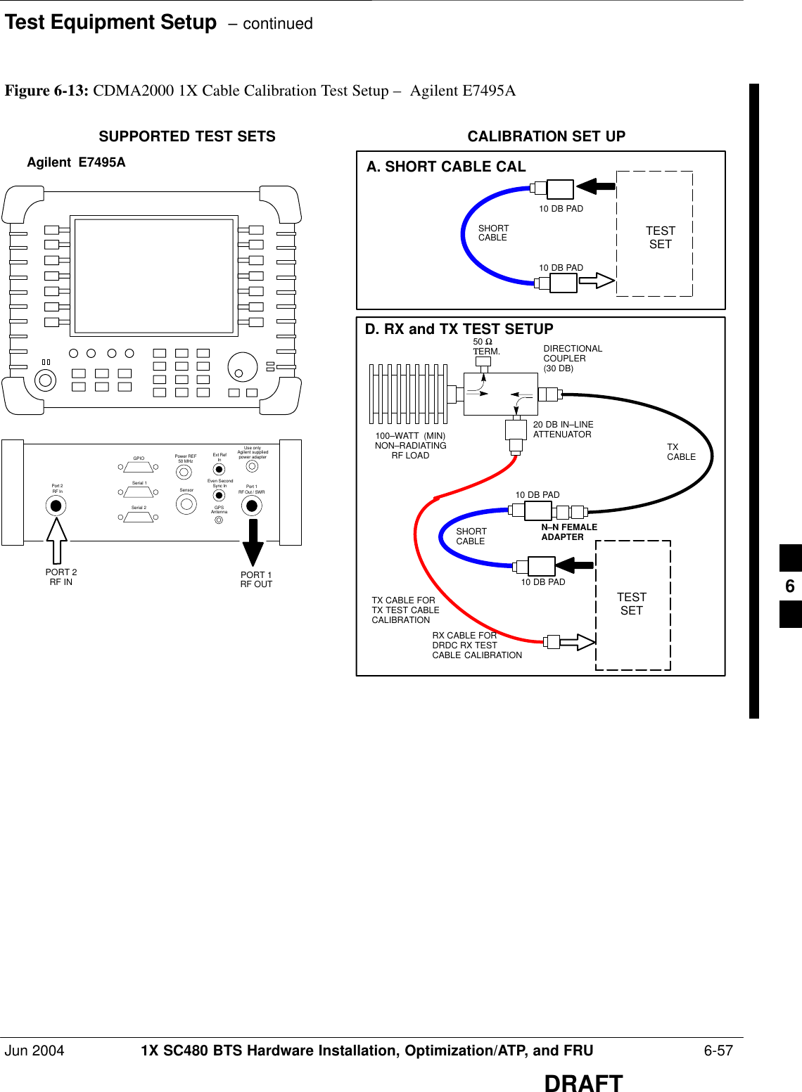
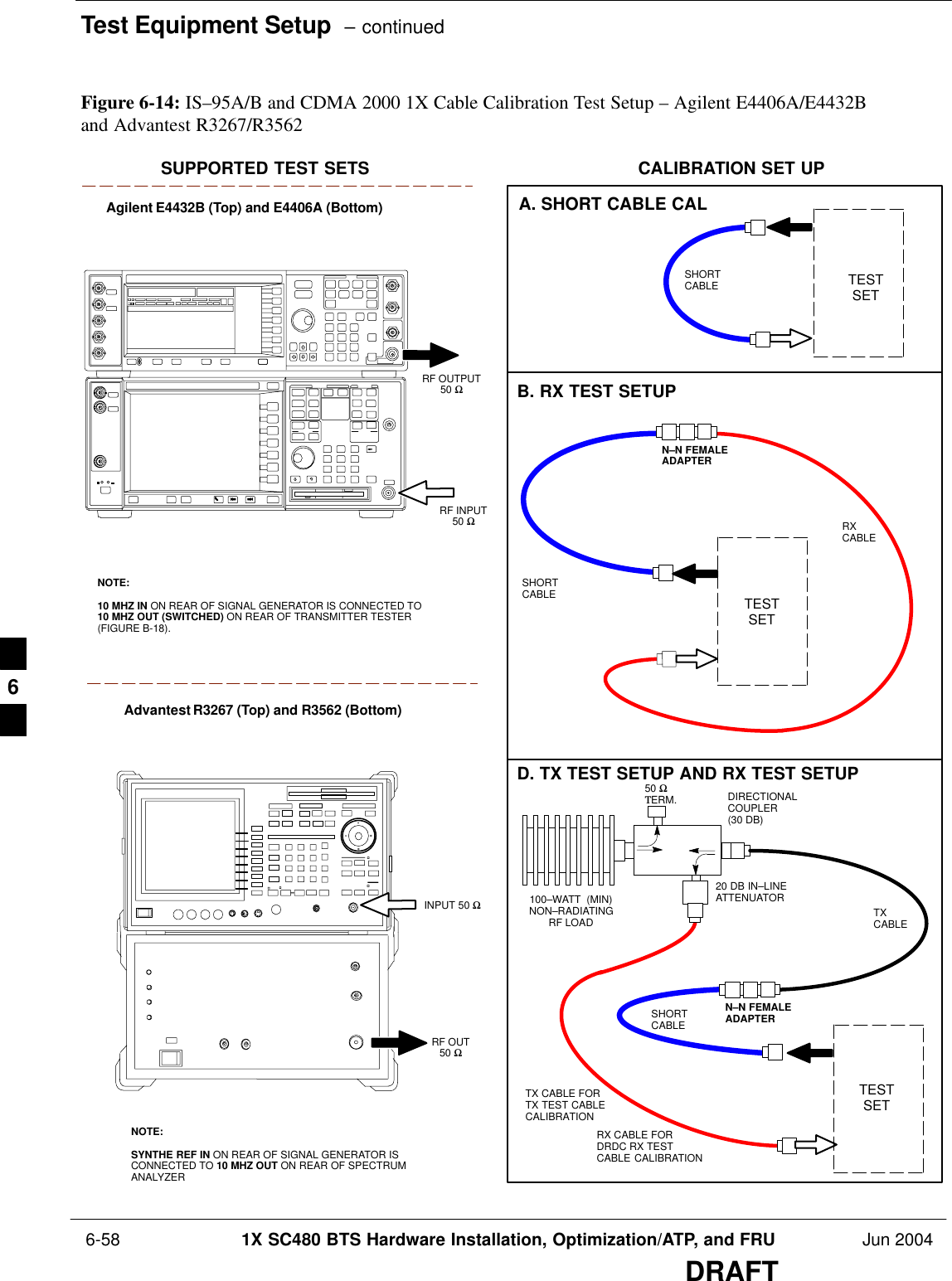
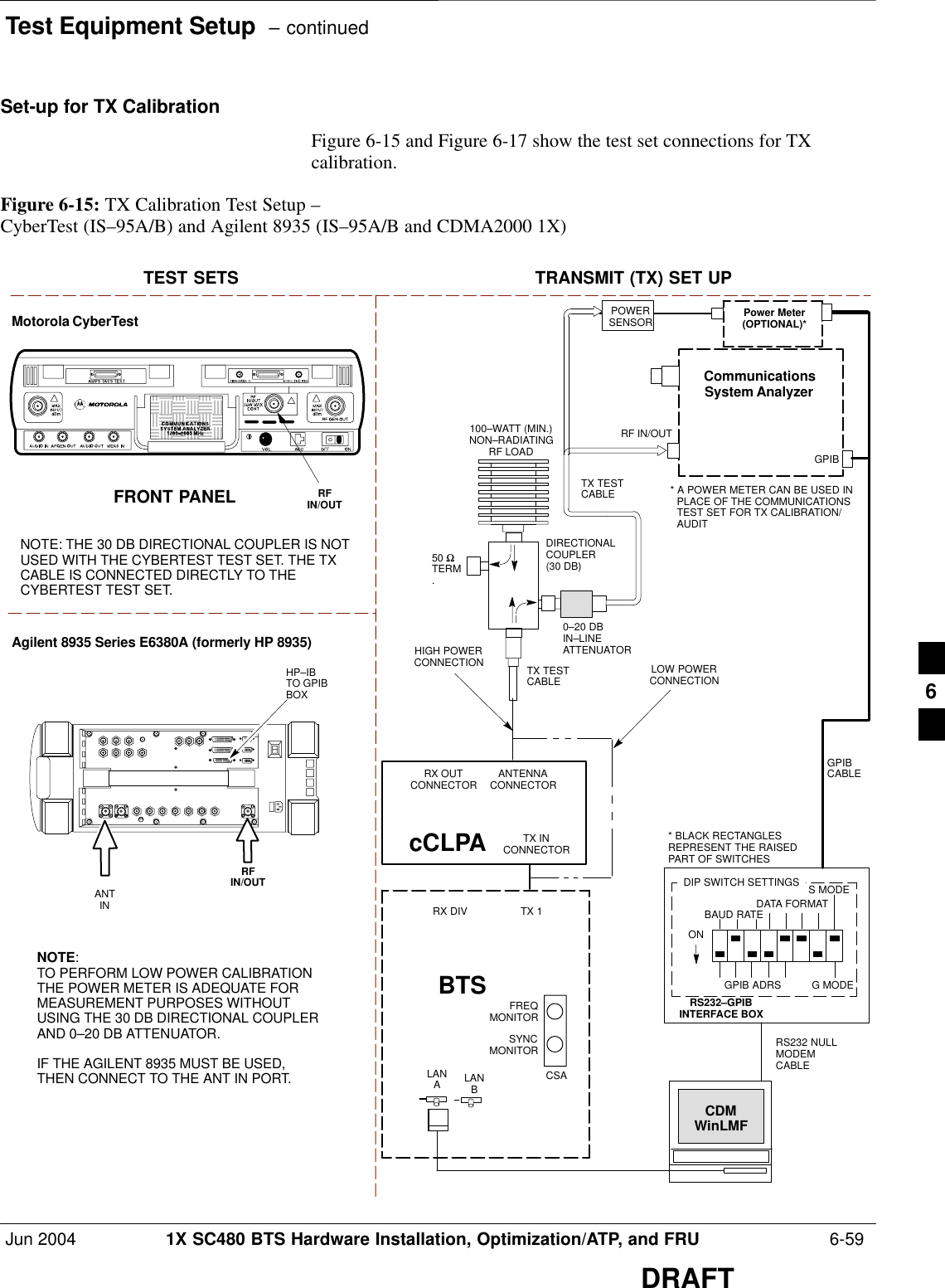
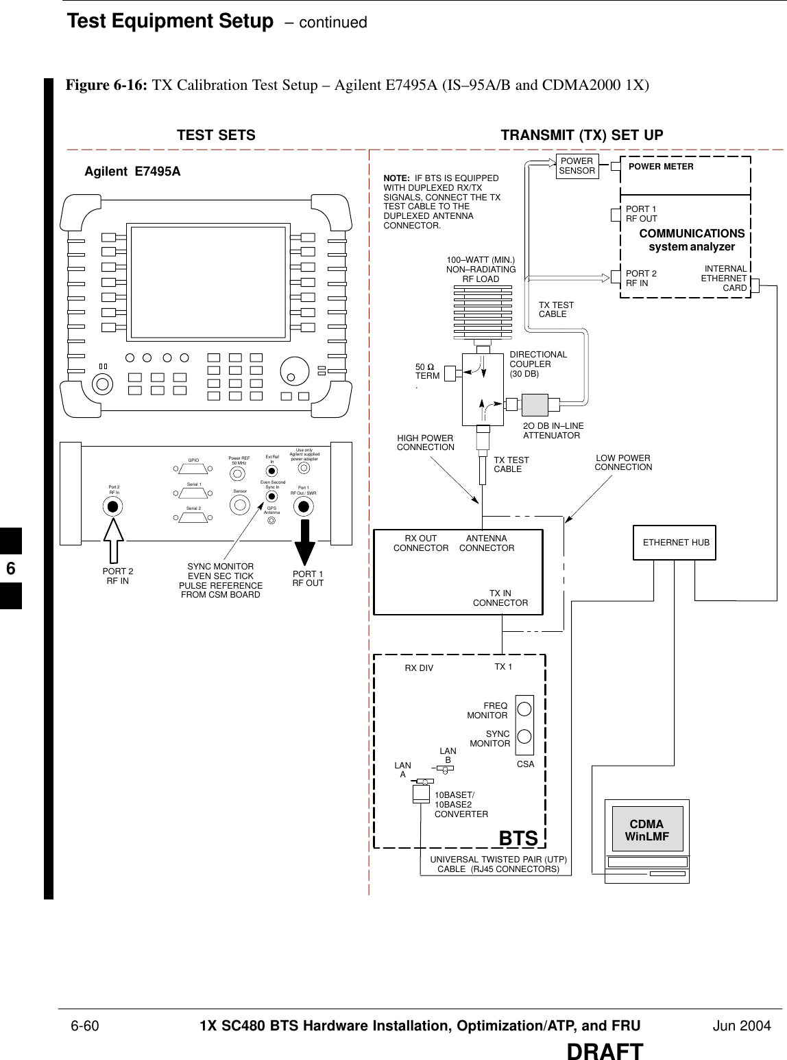
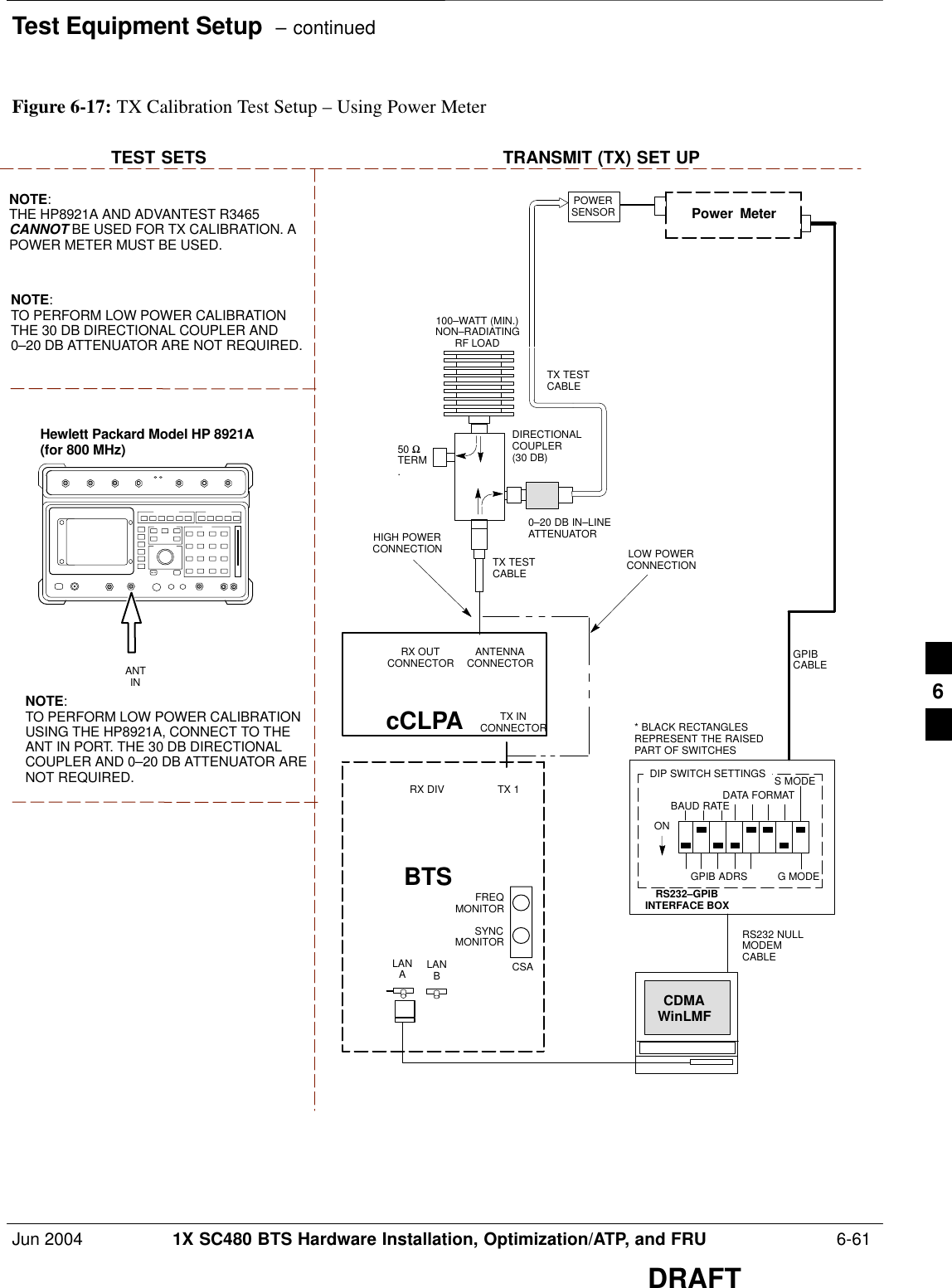
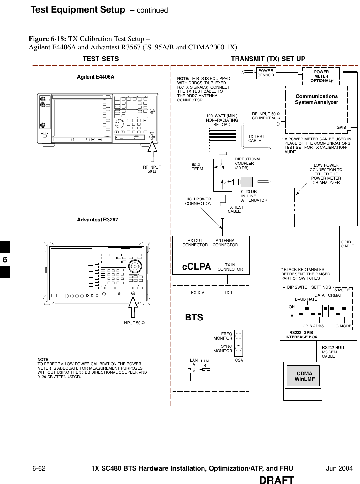
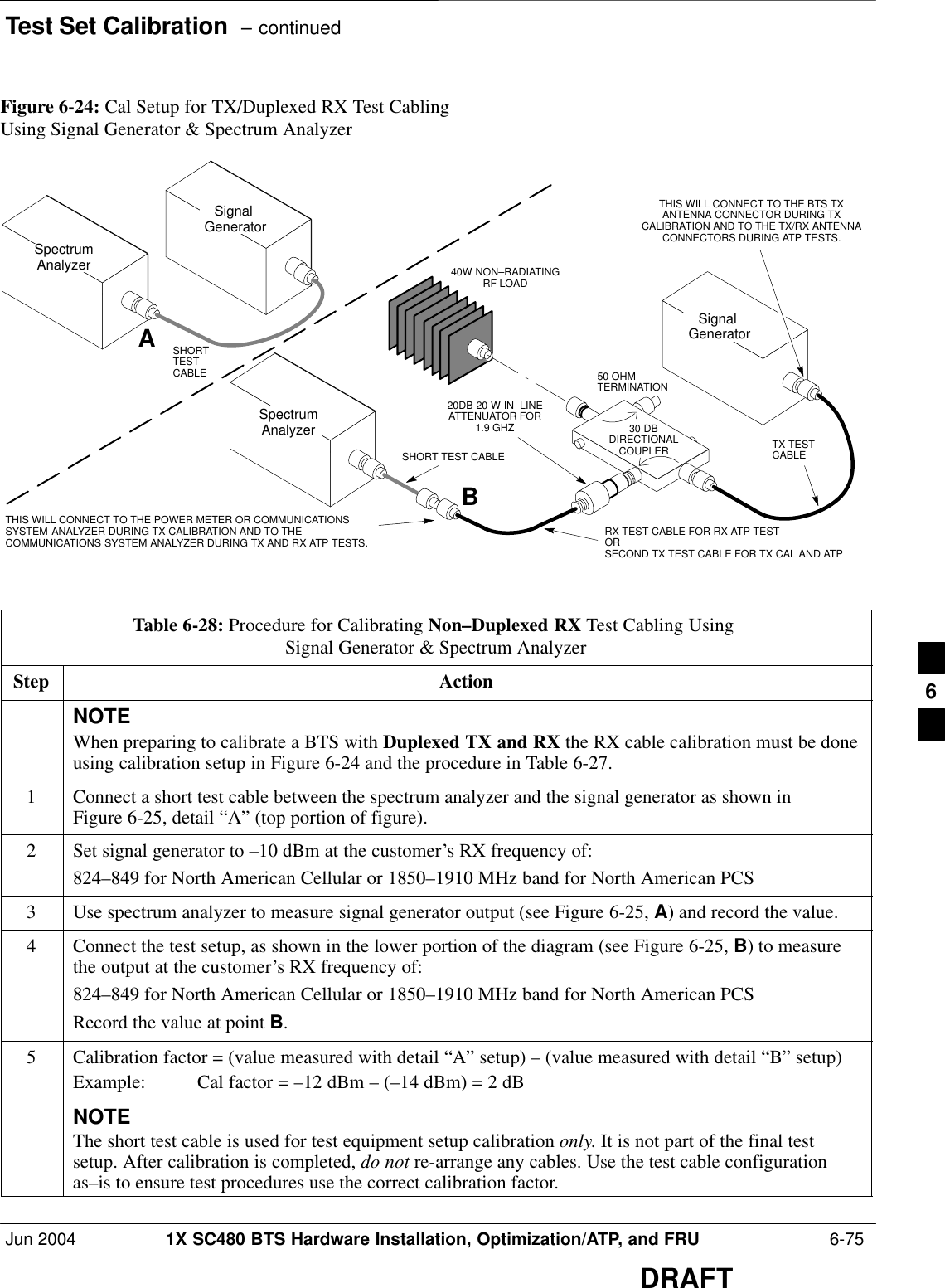
![Bay Level Offset Calibration – continuedJun 2004 1X SC480 BTS Hardware Installation, Optimization/ATP, and FRU 6-81DRAFTCAL File and BLO Data DownloadWhen BLO data is downloaded to the BBXs after calibration, the data isdownloaded to the devices in the order it is stored in the CAL file. TXcalibration data (entries C[1] – C[60]) are sent first. Data for the tenBBX slot 1 calibration points (entries C[1] – C[20]) are sent initially,followed by data for the ten BBX slot 2 calibration points (entries C[21]– C[40]), and so on. The RX calibration data is sent next in BBX slotsequence, followed by RX Diversity calibration data.BLO for Expansion BTSThe BLO Ranges for expansion BTS configurations are listed below:Low PowerS1.9 GHz: 1 to 4 carriers: –15 7 dBS1.9 GHz: 5 to 8 carriers: –19 7dBHigh Power (1 or 2 cCLPAs)S1.9 GHz: 1 to 2 carriers: 46 7 dBS1.9 GHz: 3 to 4 carriers: 42 7 dBS1.9 GHz: 5 to 8 carriers: 40 7dBTest Equipment Setup forRF Path CalibrationFollow the procedure in Table 6-31 and refer as needed to Figure 6-15 orFigure 6-17 to set up test equipment.Table 6-31: Procedure to Set Up Test Equipment for RF Path CalibrationStep Action1If it has not already been done, refer to the procedure in Table 6-6 (on page 6-17) to interface the LMFcomputer terminal to the frame LAN A connector.2If it has not already been done, refer to Table 6-7 (on page 6-25) to start a GUI LMF session.3If not already done, select test equipment per the procedure in Table 6-23 or Table 6-24.4If required, calibrate the test equipment per the procedure in Table 6-25.! CAUTIONTo prevent damage to the test equipment in high power configurations, all transmit (TX) testconnections must be via the 30 dB directional coupler for 1.9 GHz.Attenuators are not required for low power configuration.5For TX path calibration, connect the test equipment as shown in Figure 6-15, Figure 6-17, orFigure 6-18, depending on the communications analyzer being used.6](https://usermanual.wiki/Nokia-Solutions-and-Networks/T6EK1.User-Manual-2-of-4/User-Guide-448329-Page-117.png)


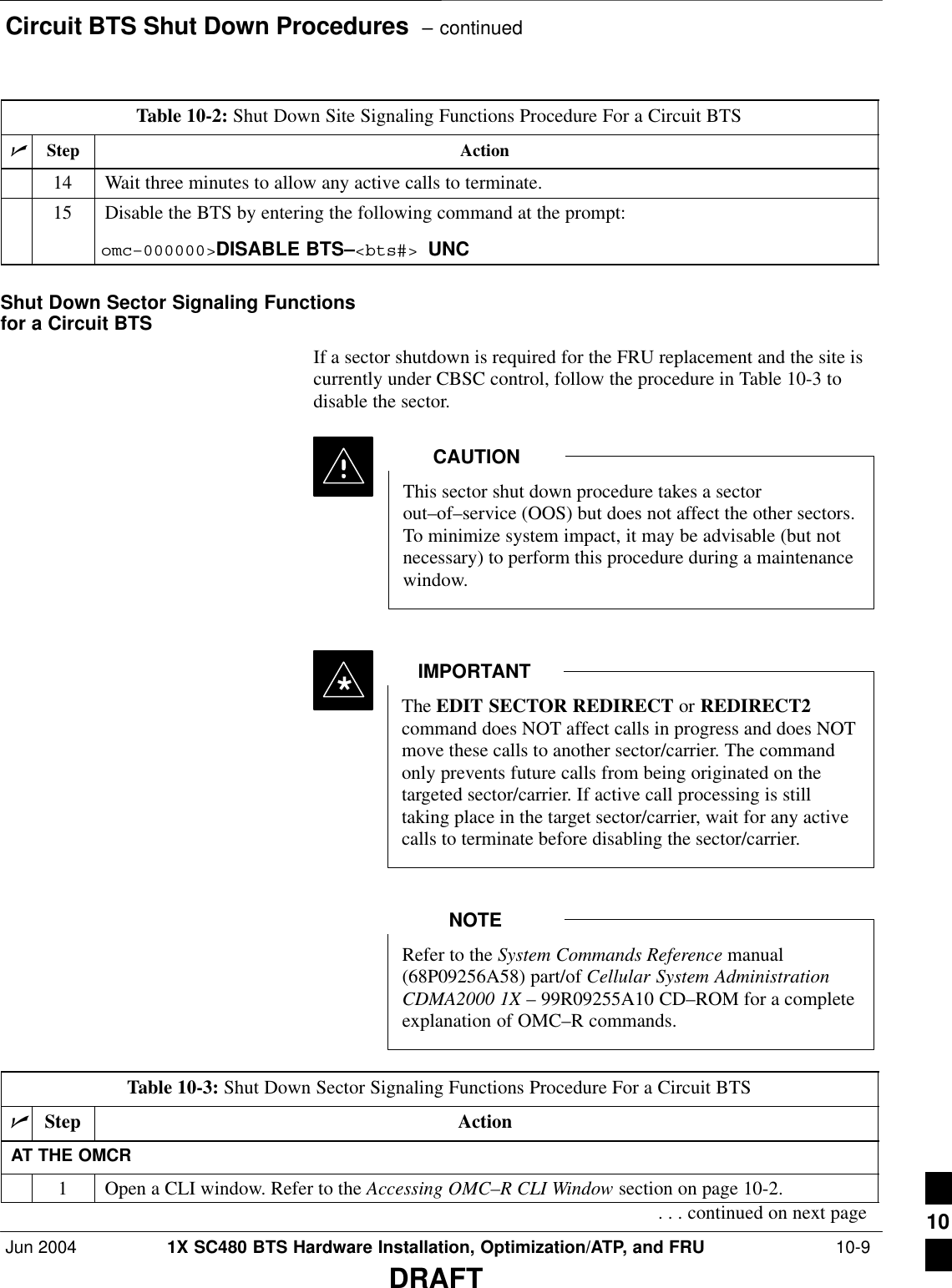
![Circuit BTS Shut Down Procedures – continuedJun 2004 1X SC480 BTS Hardware Installation, Optimization/ATP, and FRU 10-5DRAFTTable 10-2: Shut Down Site Signaling Functions Procedure For a Circuit BTSnActionStepNOTEThis step edits the REDIRECT parameters so that the Global Service Redirect Message to bebroadcast on the paging channel redirects all subscribers away from the BTS and onto a differentBTS or system.4Enter the following command at the prompt:omc–000000>EDIT BTS–<bts#> REDIRECT!The system prompts you to enter each command parameter value one at a time. Answer theprompts in the following order:<accolc0>enter Y, <accolc1>enter Y, ... <accolc15> enter Y (All Access Overload Classes must be set to yes to ensure that all subscribers are redirected.)<returniffail> , enter N(Must be set to no to ensure that subscribers do not return if redirect is unsuccessful.)<recordtype> , enter 1 or 2 (A value of 2 will invoke REDIRECT2 which is used to redirect subscribers to a CDMA channelat a neighbor site. A value of 1 redirects subscribers to an 1.9 GHz site. This example uses 2.)<expectedsid> , enter 13 (Use the Area ID the subscriber units should expect to find on the system where they are beingredirected. This example uses 13. The valid range is 0 – 32767; the default is 0.)<ignorecdma> , enter Y<sysordering> , enter CUSTOM (The system acquisition ordering value tells the mobiles the order to use when attempting toobtain service on the different analog systems. Valid values are: CUSTOM – use custom systemselection; AONLY – try the A system only; BONLY – use the B system only; AFIRST – try the Asystem first. If unsuccessful, try the B system; BFIRST – try the B system first. If unsuccessful,try the A system; AORB – try A or B. If unsuccessful try the alternative system; CUSTOM is thedefault.)<rotatetimer> , enter 4 (Call processing continuously rotates, circular right–shifts, the Y/N values of Access OverloadClass Redirect Flags 0 to 9. Values are shifted one flag at the end of the timer period; then timerre–starts. Valid values are 0–255; 4 is the default.)The system displays the command to be sent. Verify the command syntax.omc–000000>Accept [yes/no]?Enter Y to accept the command or N to go back and enter the correct value(s).. . . continued on next page10](https://usermanual.wiki/Nokia-Solutions-and-Networks/T6EK1.User-Manual-2-of-4/User-Guide-448329-Page-263.png)
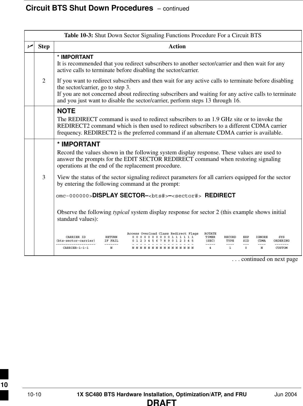
![Circuit BTS Shut Down Procedures – continuedJun 2004 1X SC480 BTS Hardware Installation, Optimization/ATP, and FRU 10-7DRAFTTable 10-2: Shut Down Site Signaling Functions Procedure For a Circuit BTSnActionStepNOTEThis step edits the REDIRECT2 parameters so that the Global Service Redirect Message to bebroadcast on the paging channel redirects all subscribers away from the BTS with the failedequipment and onto a CDMA channel at a neighbor site.8Enter the following command at the prompt:omc–000000>EDIT BTS–<bts#> REDIRECT2!The system prompts you to enter each command parameter value one at a time. Answer theprompts in the following order:expecting an integer number (from 0 to 65535)<EXPNID= ? >(Use the Network ID the subscriber units should expect to find on the system they are beingredirected to. This example uses 555.)expecting an integer number (from 0 to 2047)<CHAN1= ? >, <CHAN2= ? > ... <CHAN15= ?>(A list of CDMA channels for neighbor sites that the subscriber units can use for redirection. Thisexample uses 200, 350, 400, 725, 75, 175, 100, 575, and 775.)expecting an enumerated value: CDMA1900 CDMA800 CDMA900 JAPANCDMA CDMA2100<BANDCLASS= ? >(Use CDMA1900 for 1.9 GHz systems, and CDMA800 for 1.9 GHz systems. This example usesCDMA800.)The system displays the command to be sent. Verify the command syntax.omc–000000>Accept [yes/no]?Enter Y to accept the command or N to go back and enter the correct value(s).9View the status of the BTS signaling REDIRECT2 parameters to verify that the BTS is ready formaintenance.omc–000000>DISPLAY BTS–<bts#> REDIRECT2Ensure that the values in the system display response match the values input in Step 8 (seeexample below). REDIRECT CHAN CARRIER ID EXP BAND(bts–sector–carrier) NID CLASS 1 2 3 4 5 6 7 8 9 10 11 12 13 14 15–––––––––––––––––––– ––––– ––––––––– ––– ––– ––– ––– ––– ––– –––– –––– –––– –––– –––– –––– –––– ––– –––– CARRIER–1–1–1 555 CDMA800 200 350 400 725 75 175 100 575 775 – – – – – – . . . continued on next page10](https://usermanual.wiki/Nokia-Solutions-and-Networks/T6EK1.User-Manual-2-of-4/User-Guide-448329-Page-265.png)
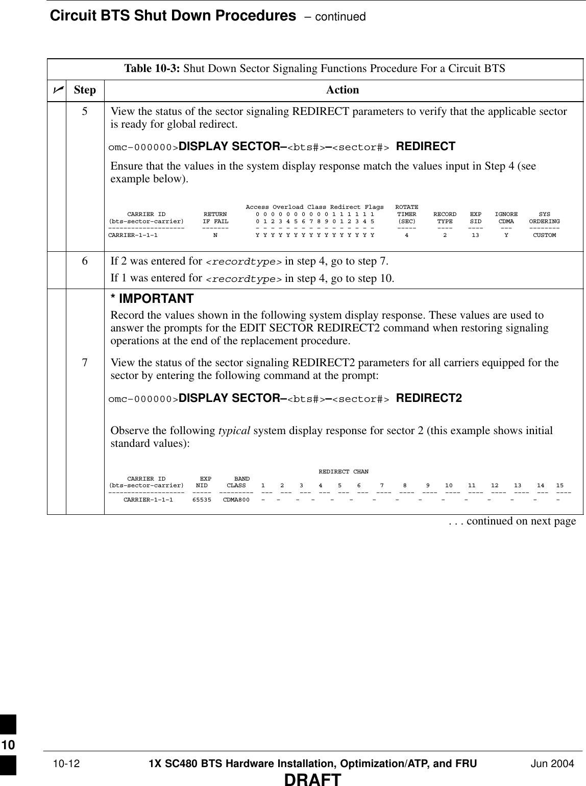
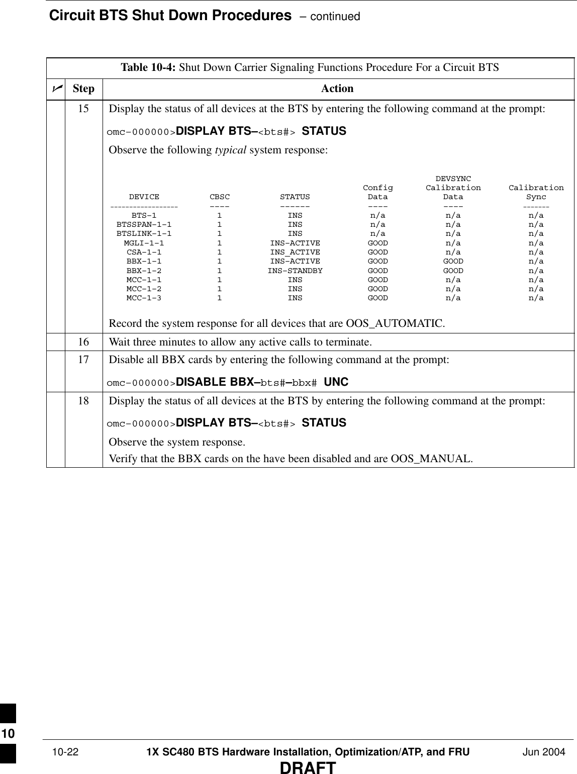
![Circuit BTS Shut Down Procedures – continued 10-8 1X SC480 BTS Hardware Installation, Optimization/ATP, and FRU Jun 2004DRAFTTable 10-2: Shut Down Site Signaling Functions Procedure For a Circuit BTSnActionStep10 View the existing congestion control parameters for all carriers equipped for the BTS by enteringthe following command at the prompt:omc–000000>DISPLAY BTS–<bts#> CONGESTCONFObserve the following typical system display response for a BTS: CARRIER NEWCALL REG AGG(bts#–sector#–carrier#) SET ALARMFLAG ALARMFLAG ALARMFLAG ANALOGREDIRECT GLOBALREDIRECT––––––––––––––––––––––– ––– ––––––––– ––––––––– ––––––––– –––––––––––––– –––––––––––––– 1–1–1 1 ENABLE ENABLE ENABLE DISABLE DISABLE NOTEIn this step, you will change the value of the Global Service Redirection Flag(GLOBALREDIRECT) in the congestion control parameters so that the Global Service RedirectMessage is broadcast on all of the sector paging channels at the BTS.11 Enter the following command at the prompt using the applicable BTS number:omc–000000>EDIT BTS –<bts#> CONGESTCONF !The system prompts you to enter each control parameter value one at a time. Skip through theprompts until you get to the following:<globalredirect> , enter ENABLE (This will force the Global Service Redirect Message to be broadcast on all of the sector pagingchannels at the BTS.)The system displays the values of the control parameters. Verify that only theGLOBALREDIRECT value changed.omc–000000>Accept [yes/no]?Enter Y to accept the change.Now the Global Service Redirection Message is sent over the sector paging channels. Allsubscribers are redirected away from the BTS and onto a different system or CDMA carrierchannel. This effectively shuts down the BTS.12 Verify that the CONGESTCONF globalredirect is enabled for each carrier at the BTS byentering the following command at the prompt:omc–000000>DISPLAY BTS–<bts#> CONGESTCONFObserve the following typical system display response for a BTS: CARRIER NEWCALL REG AGG(bts#–sector#–carrier#) SET ALARMFLAG ALARMFLAG ALARMFLAG ANALOGREDIRECT GLOBALREDIRECT––––––––––––––––––––––– ––– ––––––––– ––––––––– ––––––––– –––––––––––––– –––––––––––––– 1–1–1 1 ENABLE ENABLE ENABLE DISABLE ENABLE 13 Display the status of all devices at the BTS by entering the following command at the prompt:omc–000000>DISPLAY BTS–<bts#> STATUSRecord the system response for all devices that are OOS_AUTOMATIC. This information will beused for later reference when restoring site signaling operations.. . . continued on next page10](https://usermanual.wiki/Nokia-Solutions-and-Networks/T6EK1.User-Manual-2-of-4/User-Guide-448329-Page-266.png)
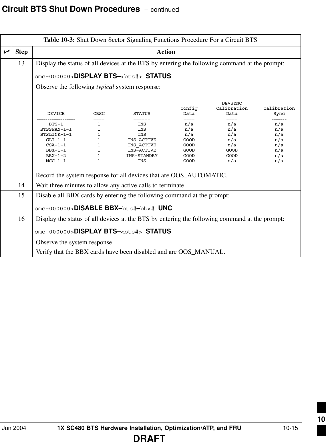
![Circuit BTS Shut Down Procedures – continuedJun 2004 1X SC480 BTS Hardware Installation, Optimization/ATP, and FRU 10-11DRAFTTable 10-3: Shut Down Sector Signaling Functions Procedure For a Circuit BTSnActionStepNOTEThis step edits the REDIRECT parameters so that the Global Service Redirect Message to bebroadcast on the paging channel redirects all subscribers away from the sector with the failedequipment and onto a different sector, BTS, or system.4Enter the following command at the prompt:omc–000000>EDIT SECTOR–<bts#>–<sector#> REDIRECT !The system prompts you to enter each command parameter value one at a time. Answer theprompts in the following order:<accolc0>enter Y, <accolc1>enter Y,... <accolc15>enter Y(All Access Overload Classes must be set to yes to ensure that all subscribers are redirected.)<returniffail> , enter N(Must be set to no to ensure that subscribers do not return if redirect is unsuccessful.)<recordtype> , enter 1 or 2 (A value of 2 will invoke REDIRECT2 which is used to redirect subscribers to a CDMA channelat a neighbor sector/site. A value of 1 redirects subscribers to an 1.9 GHz site. This example uses2.)<expectedsid> , enter 13 (Use the Area ID the subscriber units should expect to find on the system where they are beingredirected. This example uses 13. The valid range is 0 – 32767; the default is 0.)<ignorecdma> , enter Y<sysordering> , enter CUSTOM (The system acquisition ordering value tells the mobiles the order to use when attempting toobtain service on the different analog systems. Valid values are: CUSTOM – use custom systemselection; AONLY – try the A system only; BONLY – use the B system only; AFIRST – try the Asystem first. If unsuccessful, try the B system; BFIRST – try the B system first. If unsuccessful,try the A system; AORB – try A or B. If unsuccessful try the alternative system; CUSTOM is thedefault.)<rotatetimer> , enter 4 (Call processing continuously rotates, circular right–shifts, the Y/N values of Access OverloadClass Redirect Flags 0 to 9. Values are shifted one flag at the end of the timer period; then timerre–starts. Valid values are 0–255; 4 is the default.)The system displays the command to be sent. Verify the command syntax.omc–000000>Accept [yes/no]?Enter Y to accept the command or N to go back and enter the correct value(s).. . . continued on next page10](https://usermanual.wiki/Nokia-Solutions-and-Networks/T6EK1.User-Manual-2-of-4/User-Guide-448329-Page-269.png)
![Circuit BTS Shut Down Procedures – continuedJun 2004 1X SC480 BTS Hardware Installation, Optimization/ATP, and FRU 10-13DRAFTTable 10-3: Shut Down Sector Signaling Functions Procedure For a Circuit BTSnActionStepNOTEThis step edits the REDIRECT2 parameters so that the Global Service Redirect Message to bebroadcast on the paging channel redirects all subscribers away from the sector with the failedequipment and onto a CDMA channel at a neighbor sector/site.8Enter the following command at the prompt:omc–000000>EDIT SECTOR–<bts#>–<sector#> REDIRECT2 !The system prompts you to enter each command parameter value one at a time. Answer theprompts in the following order:expecting an integer number (from 0 to 65535)<EXPNID= ? >(Use the Network ID the subscriber units should expect to find on the system they are beingredirected to. This example uses 555.)expecting an integer number (from 0 to 2047)<CHAN1= ? >, <CHAN2= ? > ... <CHAN15= ?>(A list of CDMA channels for neighbor sites that the subscriber units can use for redirection. Thisexample uses 200, 350, 400, 725, 75, 175, 100, 575, and 775.)expecting an enumerated value: CDMA1900 CDMA800 CDMA900 JAPANCDMA CDMA2100<BANDCLASS= ? >(Use CDMA1900 for 1.9 GHz systems, and CDMA800 for 800 MHz systems. This example usesCDMA1900.)The system displays the command to be sent. Verify the command syntax.omc–000000>Accept [yes/no]?Enter Y to accept the command or N to go back and enter the correct value(s).9View the status of the sector signaling REDIRECT2 parameters to verify that the sector is readyfor maintenance.omc–000000>DISPLAY SECTOR–<bts#>–<sector#> REDIRECT2Ensure that the values in the system display response match the values input in Step 8 (seeexample below). REDIRECT CHAN CARRIER ID EXP BAND(bts–sector–carrier) NID CLASS 1 2 3 4 5 6 7 8 9 10 11 12 13 14 15–––––––––––––––––––– ––––– ––––––––– ––– ––– ––– ––– ––– ––– –––– –––– –––– –––– –––– –––– –––– ––– –––– CARRIER–1–1–1 555 CDMA800 200 350 400 725 75 175 100 575 775 – – – – – – . . . continued on next page10](https://usermanual.wiki/Nokia-Solutions-and-Networks/T6EK1.User-Manual-2-of-4/User-Guide-448329-Page-271.png)
![Circuit BTS Shut Down Procedures – continued 10-14 1X SC480 BTS Hardware Installation, Optimization/ATP, and FRU Jun 2004DRAFTTable 10-3: Shut Down Sector Signaling Functions Procedure For a Circuit BTSnActionStep10 View the existing congestion control parameters for all carriers equipped for the applicable sectorby entering the following command at the prompt:omc–000000>DISPLAY SECTOR–<bts#>–<sector#> CONGESTCONFObserve the following typical system display response for sector 2:CARRIER NEWCALL REG AGG(bts#–sector#–carrier#) SET ALARMFLAG ALARMFLAG ALARMFLAG ANALOGREDIRECT GLOBALREDIRECT––––––––––––––––––––––– ––– ––––––––– –––––––––– –––––––––– –––––––––––––– ––––––––––––––1–1–1 1 ENABLE ENABLE ENABLE DISABLE DISABLENOTEIn this step, you will change the value of the Global Service Redirection Flag(GLOBALREDIRECT) in the congestion control parameters so that the Global Service RedirectMessage is broadcast on the sector paging channel.11 Enter the following command at the prompt:omc–000000>EDIT SECTOR–<bts#>–<sector#> CONGESTCONF !The system prompts you to enter each control parameter value one at a time. Skip through theprompts until you get to the following:<globalredirect> , enter ENABLE (This forces the Global Service Redirect Message to be broadcast on the sector paging channel.)The system displays the values of the control parameters. Verify that only theGLOBALREDIRECT value changed.omc–000000>Accept [yes/no]?Enter Y to accept the change.Now the Global Service Redirection Message is sent over the sector paging channels. Allsubscribers are redirected away from the sector and onto a different system. This effectively shutsdown the sector.12 Verify that the CONGESTCONF globalredirect is enabled for each carrier on the sector byentering the following command at the prompt:omc–000000>DISPLAY SECTOR–<bts#>–<sector#> CONGESTCONFObserve the following typical system display response for sector 2:CARRIER NEWCALL REG AGG(bts#–sector#–carrier#) SET ALARMFLAG ALARMFLAG ALARMFLAG ANALOGREDIRECT GLOBALREDIRECT––––––––––––––––––––––– ––– ––––––––– –––––––––– –––––––––– –––––––––––––– ––––––––––––––1–1–1 1 ENABLE ENABLE ENABLE DISABLE ENABLE. . . continued on next page10](https://usermanual.wiki/Nokia-Solutions-and-Networks/T6EK1.User-Manual-2-of-4/User-Guide-448329-Page-272.png)
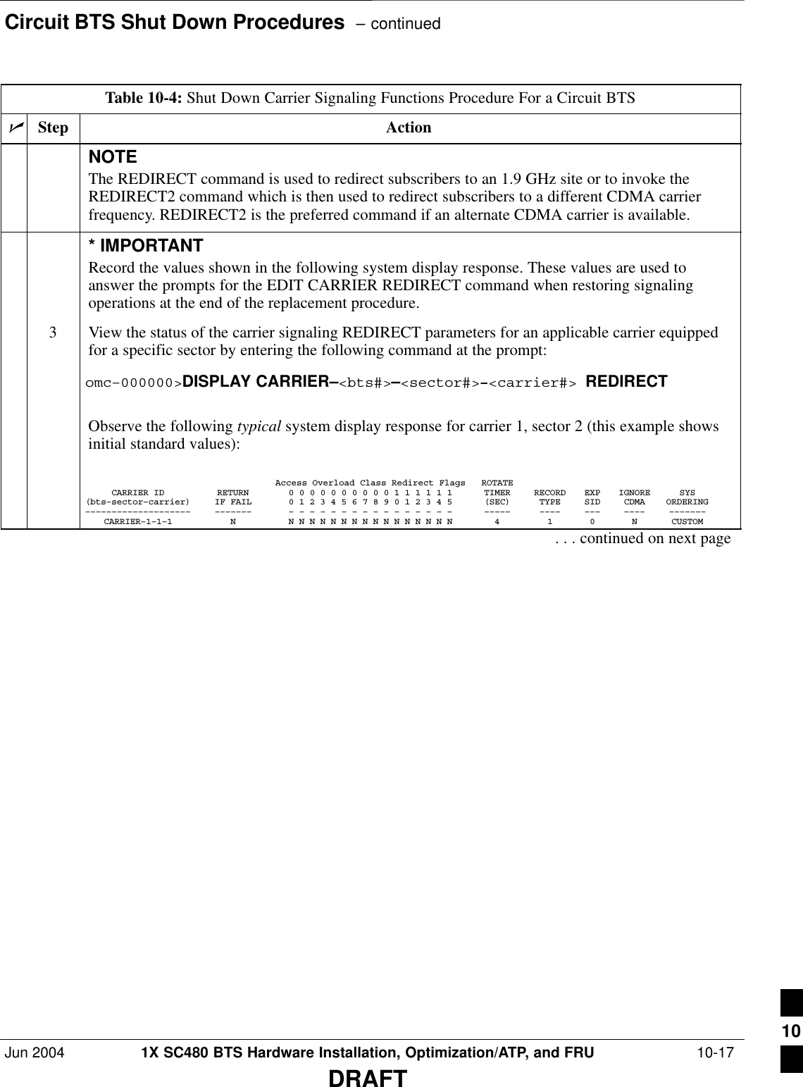
![Circuit BTS Shut Down Procedures – continued 10-18 1X SC480 BTS Hardware Installation, Optimization/ATP, and FRU Jun 2004DRAFTTable 10-4: Shut Down Carrier Signaling Functions Procedure For a Circuit BTSnActionStepNOTEThis step edits the REDIRECT parameters so that the Global Service Redirect Message to bebroadcast on the paging channel redirects subscribers assigned to the sector carrier away from thecarrier/sector with the failed equipment and onto a different carrier, sector, BTS, or system.4Enter the following command at the prompt:omc–000000>EDIT CARRIER–<bts#>–<sector#>–<carrier#> REDIRECT !The system prompts you to enter each command parameter value one at a time. Answer theprompts in the following order:<accolc0>enter Y, <accolc1>enter Y,... <accolc15>enter Y(All Access Overload Classes must be set to yes to ensure that all subscribers are redirected.)<returniffail> , enter N(Must be set to no to ensure that subscribers do not return if redirect is unsuccessful.)<recordtype> , enter 1 or 2 (A value of 2 will invoke REDIRECT2 which is used to redirect subscribers to a CDMA channelat a neighbor sector/site. A value of 1 redirects subscribers to an 1.9 GHz site. This example uses2.)<expectedsid> , enter 13 (Use the Area ID the subscriber units should expect to find on the system where they are beingredirected. This example uses 13. The valid range is 0 – 32767; the default is 0.)<ignorecdma> , enter Y<sysordering> , enter CUSTOM (The system acquisition ordering value tells the mobiles the order to use when attempting toobtain service on the different analog systems. Valid values are: CUSTOM – use custom systemselection; AONLY – try the A system only; BONLY – use the B system only; AFIRST – try the Asystem first. If unsuccessful, try the B system; BFIRST – try the B system first. If unsuccessful,try the A system; AORB – try A or B. If unsuccessful try the alternative system; CUSTOM is thedefault.)<rotatetimer> , enter 4 (Call processing continuously rotates, circular right–shifts, the Y/N values of Access OverloadClass Redirect Flags 0 to 9. Values are shifted one flag at the end of the timer period; then timerre–starts. Valid values are 0–255; 4 is the default.)The system displays the command to be sent. Verify the command syntax.omc–000000>Accept [yes/no]?Enter Y to accept the command or N to go back and enter the correct value(s).. . . continued on next page10](https://usermanual.wiki/Nokia-Solutions-and-Networks/T6EK1.User-Manual-2-of-4/User-Guide-448329-Page-276.png)
![Circuit BTS Shut Down Procedures – continued 10-20 1X SC480 BTS Hardware Installation, Optimization/ATP, and FRU Jun 2004DRAFTTable 10-4: Shut Down Carrier Signaling Functions Procedure For a Circuit BTSnActionStepNOTEThis step edits the redirect parameters so that the Global Service Redirect Message to be broadcaston the paging channel redirects all subscribers away from the carrier with the failed equipment andonto a different CDMA carrier frequency.9Enter the following command at the prompt:omc–000000>EDIT CARRIER–<bts#>–<sector#>–<carrier#> REDIRECT2 !The system prompts you to enter each command parameter value one at a time. Answer theprompts in the following order:expecting an integer number (from 0 to 65535)<EXPNID= ? >(Use the Network ID the subscriber units should expect to find on the system they are beingredirected to. This example uses 555.)expecting an integer number (from 0 to 2047)<CHAN1= ? >, <CHAN2= ? > ... <CHAN15= ?>(A list of CDMA channels for neighbor sites that the subscriber units can use for redirection. Thisexample uses 200, 350, 400, 725, 75, 175, 100, 575, and 775.)expecting an enumerated value: CDMA1900 CDMA800 CDMA900 JAPANCDMA CDMA2100<BANDCLASS= ? >(Use CDMA1900 for 1.9 GHz systems, and CDMA800 for 800 MHz systems. This example usesCDMA1900.)The system displays the command to be sent. Verify the command syntax.omc–000000>Accept [yes/no]?Enter Y to accept the command or N to go back and enter the correct value(s).10 View the status of the carrier signaling redirect parameters to verify that the sector is ready formaintenance.omc–000000>DISPLAY CARRIER–<bts#>–<sector#>–<carrier#> REDIRECT2Ensure that the values in the system display response match the values input in Step 9 (seeexample below). REDIRECT CHAN CARRIER ID EXP BAND(bts–sector–carrier) NID CLASS 1 2 3 4 5 6 7 8 9 10 11 12 13 14 15–––––––––––––––––––– ––––– ––––––––– ––– ––– ––– ––– ––– ––– –––– –––– –––– –––– –––– –––– –––– ––– –––– CARRIER–1–1–1 555 CDMA800 200 350 400 725 75 175 100 575 775 – – – – – – 11 Repeat Steps 8 through 10 as required for other sectors with this carrier.. . . continued on next page10](https://usermanual.wiki/Nokia-Solutions-and-Networks/T6EK1.User-Manual-2-of-4/User-Guide-448329-Page-278.png)
![Circuit BTS Shut Down Procedures – continuedJun 2004 1X SC480 BTS Hardware Installation, Optimization/ATP, and FRU 10-21DRAFTTable 10-4: Shut Down Carrier Signaling Functions Procedure For a Circuit BTSnActionStep12 View the existing congestion control parameters for the applicable carrier equipped for a specificsector by entering the following command at the prompt:omc–000000>DISPLAY CARRIER–<bts#>–<sector#>–<carrier#> CONGESTCONFObserve the following typical system display response for carrier 1, sector 2:CARRIER NEWCALL REG AGG(bts#–sector#–carrier#) SET ALARMFLAG ALARMFLAG ALARMFLAG ANALOGREDIRECT GLOBALREDIRECT––––––––––––––––––––––– ––– ––––––––– –––––––––– –––––––––– –––––––––––––– ––––––––––––––146–2–1 1 ENABLE ENABLE ENABLE DISABLE DISABLENOTEIn this step, you will change the value of the Global Service Redirection Flag(GLOBALREDIRECT) in the congestion control parameters so that the Global Service RedirectMessage is broadcast on the sector paging channel of a specific carrier.13 Enter the following command at the prompt using the carrier number and the applicable sectornumber:omc–000000>EDIT CARRIER–<bts#>–<sector#>–<carrier#> CONGESTCONF !The system prompts you to enter each control parameter value one at a time. Skip through theprompts until you get to the following:<globalredirect> , enter ENABLE (This will force the Global Service Redirect Message to be broadcast on the sector pagingchannel.)The system displays the values of the control parameters. Verify that only theGLOBALREDIRECT value changed.omc–000000>Accept [yes/no]?Enter Y to accept the change.Now the Global Service Redirection Message is sent over the sector paging channel. Allsubscribers are redirected away from the carrier/sector and onto a different system. This effectivelyshuts down the carrier/sector.14 Repeat Steps 12 and 13 as required for other sectors, selecting the proper sector number for thesector# parameter.. . . continued on next page10](https://usermanual.wiki/Nokia-Solutions-and-Networks/T6EK1.User-Manual-2-of-4/User-Guide-448329-Page-279.png)
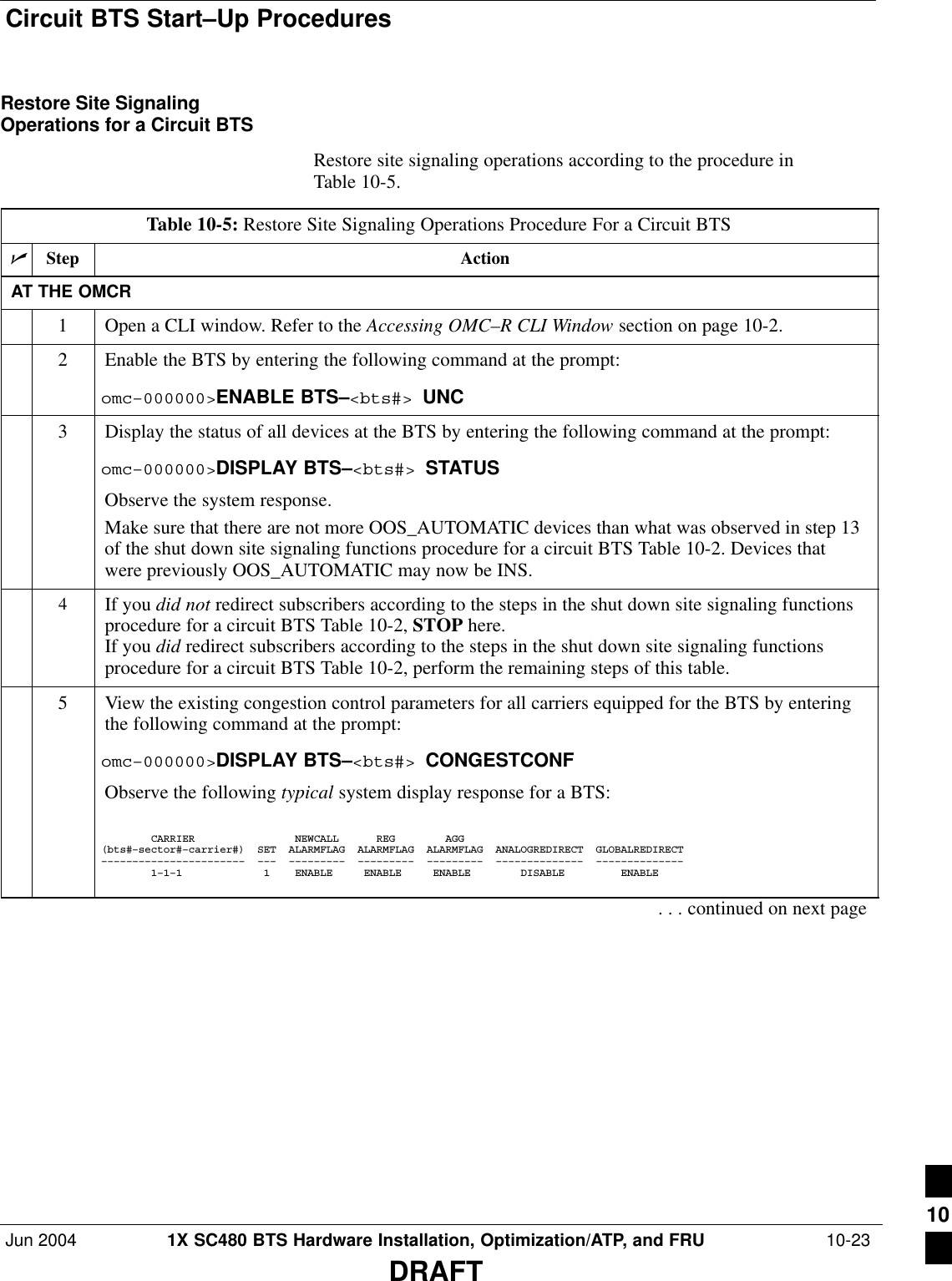
![Circuit BTS Start–Up Procedures – continued 10-24 1X SC480 BTS Hardware Installation, Optimization/ATP, and FRU Jun 2004DRAFTTable 10-5: Restore Site Signaling Operations Procedure For a Circuit BTSnActionStepNOTEIn this step, you will change the value of the Global Service Redirection Flag(GLOBALREDIRECT) in the congestion control parameters so that the Global Service RedirectMessage is only broadcast on the sector paging channel when there is traffic congestion in thesector.6Enter the following command at the prompt using the applicable BTS number:omc–000000>EDIT BTS –<bts#> CONGESTCONF !The system prompts you to enter each control parameter value one at a time. Skip through theprompts until you get to the following:<globalredirect> , enter DISABLE (This will revert the Global Service Redirect Message to congestion control.)The system displays the values of the control parameters. Verify that only theGLOBALREDIRECT value changed.omc–000000>Accept [yes/no]?Enter Y to accept the change.Now the Global Service Redirection Message will only be sent over the sector paging channelswhen there is traffic congestion in the sector.7Enter the following command at the prompt:omc–000000>DISPLAY BTS–<bts#> CONGESTCONFObserve the system display response.Verify that the CONGESTCONF globalredirect is disabled for each carrier at the BTS.8View the status of the signaling REDIRECT parameters for all carriers equipped for the applicableBTS by entering the following command at the prompt:omc–000000>DISPLAY BTS–<bts#> REDIRECTObserve that the values in the system display response should match the values input in step 4 ofthe shut down site signaling functions procedure for a circuit BTS Table 10-2 (see examplebelow).Access Overload Class Redirect Flags ROTATECARRIER ID RETURN 0 0 0 0 0 0 0 0 0 0 1 1 1 1 1 1 TIMER RECORD EXP IGNORE SYS(bts–sector–carrier) IF FAIL 0 1 2 3 4 5 6 7 8 9 0 1 2 3 4 5 (SEC) TYPE SID CDMA ORDERING–––––––––––––––––––– ––––––– – – – – – – – – – – – – – – – – ––––– –––– –––– ––– –––––––– CARRIER–1–1–1 N Y Y Y Y Y Y Y Y Y Y Y Y Y Y Y Y 4 2 13 Y CUSTOM . . . continued on next page10](https://usermanual.wiki/Nokia-Solutions-and-Networks/T6EK1.User-Manual-2-of-4/User-Guide-448329-Page-282.png)
![Circuit BTS Start–Up Procedures – continuedJun 2004 1X SC480 BTS Hardware Installation, Optimization/ATP, and FRU 10-25DRAFTTable 10-5: Restore Site Signaling Operations Procedure For a Circuit BTSnActionStep* IMPORTANTIn this step, use the values recorded in step 3 of the shut down site signaling functions procedurefor a circuit BTS Table 10-2 to answer the prompts for the EDIT BTS REDIRECT command;except for record type enter 2.NOTEThis step shows the entry of initial standard values which is consistent with the original example;except record type must be 2. Your entries may be different.9Restore the values of all REDIRECT parameters by entering the following command at theprompt:omc–000000>EDIT BTS–<bts#> REDIRECT !The system will prompt you to enter each command parameter one at a time. Answer the promptsin the following order (Note that the following specified values are consistent with the originalexample. Yours may be different):<accolc0> enter N, <accolc1>enter N, ... <accolc15>enter N<returniffail> , enter N<recordtype> , enter 2<expectedsid> , enter 0<ignorecdma> , enter N<sysordering> , enter CUSTOM<rotatetimer> , enter 4The system will display the command that will be sent. Verify the command syntax.omc–000000>Accept [yes/no]?Enter Y to accept the command or N to go back and enter the correct value(s).10 View the status of the signaling REDIRECT parameters by entering the following command at theprompt:omc–000000>DISPLAY BTS–<bts#> REDIRECTEnsure that the values in the system display response match the values input by the operator instep 9 (see example below). Access Overload Class Redirect Flags RETURN ROTATE RECORD EXP IGNORE SYS CARRIER ID IF FAIL 0 0 0 0 0 0 0 0 0 0 1 1 1 1 1 1 TIMER TYPE SID CDMA ORDERING(bts–sector–carrier) 0 1 2 3 4 5 6 7 8 9 0 1 2 3 4 5 (sec)–––––––––––––––––––– ––––––– – – – – – – – – – – – – – – – – –––––– –––––– ––––– –––––– –––––––– CARRIER–1 –1–1 N N N N N N N N N N N N N N N N N 4 2 0 N CUSTOM 10](https://usermanual.wiki/Nokia-Solutions-and-Networks/T6EK1.User-Manual-2-of-4/User-Guide-448329-Page-283.png)
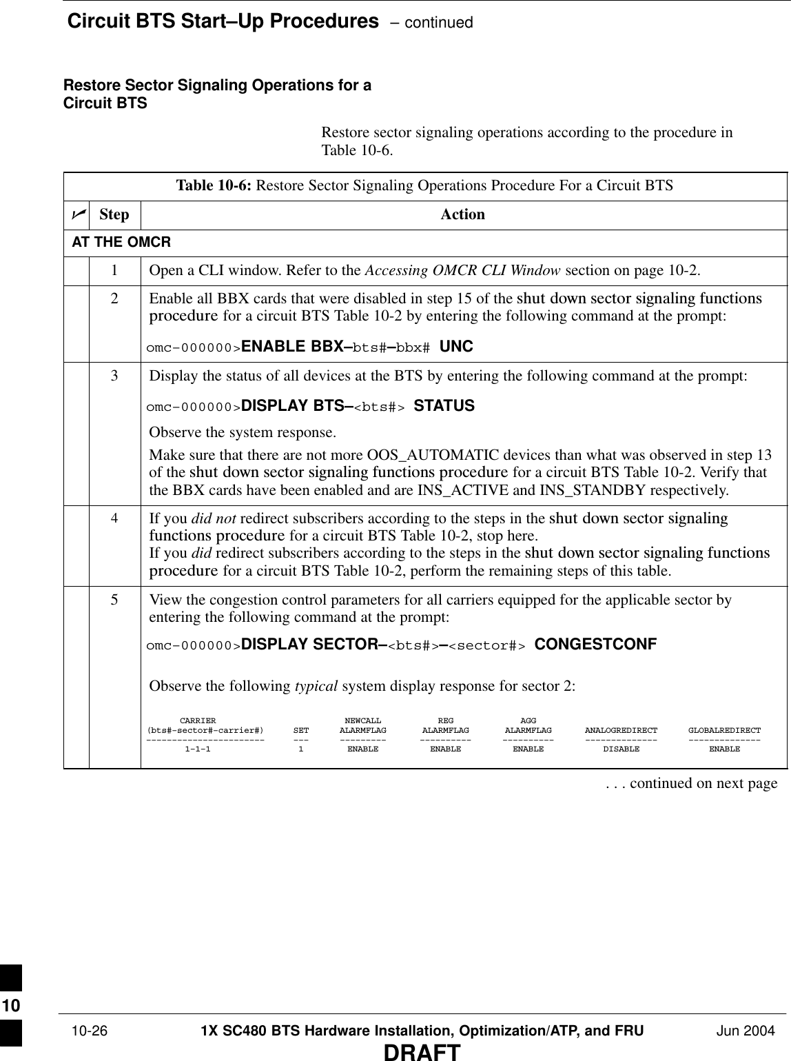
![Circuit BTS Start–Up Procedures – continuedJun 2004 1X SC480 BTS Hardware Installation, Optimization/ATP, and FRU 10-27DRAFTTable 10-6: Restore Sector Signaling Operations Procedure For a Circuit BTSnActionStepNOTEIn this step, you will change the value of the Global Service Redirection Flag(GLOBALREDIRECT) in the congestion control parameters so that the Global Service RedirectMessage is only broadcast on the sector paging channel when there is traffic congestion in thesector.6Enter the following command at the prompt using the applicable sector number:omc–000000>EDIT SECTOR–<bts#>–<sector#> CONGESTCONF !The system will prompt you to enter each control parameter value one at a time. Skip through theprompts until you get to the following:<globalredirect> , enter DISABLE (This will revert the Global Service Redirect Message to congestion control.)The system will display the values of the control parameters. Verify that only theGLOBALREDIRECT value changed.omc–000000>Accept [yes/no]?Enter Y to accept the change.Now the Global Service Redirection Message will only be sent over the sector paging channelswhen there is traffic congestion in the sector.7Enter the following command at the prompt:omc–000000>DISPLAY SECTOR–<bts#>–<sector#> CONGESTCONFObserve the system display response.Verify that the CONGESTCONF globalredirect is disabled for each carrier on the sector.8View the status of the sector signaling REDIRECT parameters for all carriers equipped for theapplicable sector by entering the following command at the prompt:omc–000000>DISPLAY SECTOR–<bts#>–<sector#> REDIRECTObserve that the values in the system display response should match the values input in step 4 ofthe shut down sector signaling functions procedure for a circuit BTS Table 10-2 (see examplebelow).Access Overload Class Redirect Flags ROTATECARRIER ID RETURN 0 0 0 0 0 0 0 0 0 0 1 1 1 1 1 1 TIMER RECORD EXP IGNORE SYS(bts–sector–carrier) IF FAIL 0 1 2 3 4 5 6 7 8 9 0 1 2 3 4 5 (SEC) TYPE SID CDMA ORDERING–––––––––––––––––––– ––––––– – – – – – – – – – – – – – – – – ––––– –––– –––– ––– ––––––––CARRIER–1–1–1 N Y Y Y Y Y Y Y Y Y Y Y Y Y Y Y Y 4 2 13 Y CUSTOM. . . continued on next page10](https://usermanual.wiki/Nokia-Solutions-and-Networks/T6EK1.User-Manual-2-of-4/User-Guide-448329-Page-285.png)
![Circuit BTS Start–Up Procedures – continued 10-28 1X SC480 BTS Hardware Installation, Optimization/ATP, and FRU Jun 2004DRAFTTable 10-6: Restore Sector Signaling Operations Procedure For a Circuit BTSnActionStep* IMPORTANTIn this step, use the values recorded in step 3 of the shut down sector signaling functionsprocedure for a circuit BTS Table 10-2 to answer the prompts for the EDIT SECTORREDIRECT command; except for record type enter 2.NOTEThis step shows the entry of initial standard values which is consistent with the original example;except record type must be 2. Your entries may be different.9Restore the values of all REDIRECT parameters by entering the following command at theprompt:omc–000000>EDIT SECTOR–<bts#>–<sector#> REDIRECT !The system will prompt you to enter each command parameter one at a time. Answer the promptsin the following order (Note that the following specified values are consistent with the originalexample. Yours may be different):<accolc0> enter N, <accolc1>enter N, ... <accolc15>enter N<returniffail> , enter N<recordtype> , enter 2<expectedsid> , enter 0<ignorecdma> , enter N<sysordering> , enter CUSTOM<rotatetimer> , enter 4The system will display the command that will be sent. Verify the command syntax.omc–000000>Accept [yes/no]?Enter Y to accept the command or N to go back and enter the correct value(s).10 View the status of the sector signaling REDIRECT parameters by entering the following commandat the prompt:omc–000000>DISPLAY SECTOR–<bts#>–<sector#> REDIRECTEnsure that the values in the system display response match the values input by the operator instep 9 (see example below).Access Overload Class Redirect Flags ROTATECARRIER ID RETURN 0 0 0 0 0 0 0 0 0 0 1 1 1 1 1 1 TIMER RECORD EXP IGNORE SYS(bts–sector–carrier) IF FAIL 0 1 2 3 4 5 6 7 8 9 0 1 2 3 4 5 (SEC) TYPE SID CDMA ORDERING–––––––––––––––––––– ––––––– – – – – – – – – – – – – – – – – ––––– –––– ––– –––– –––––––CARRIER–1–1–1 N N N N N N N N N N N N N N N N N 4 2 0 N CUSTOM 10](https://usermanual.wiki/Nokia-Solutions-and-Networks/T6EK1.User-Manual-2-of-4/User-Guide-448329-Page-286.png)
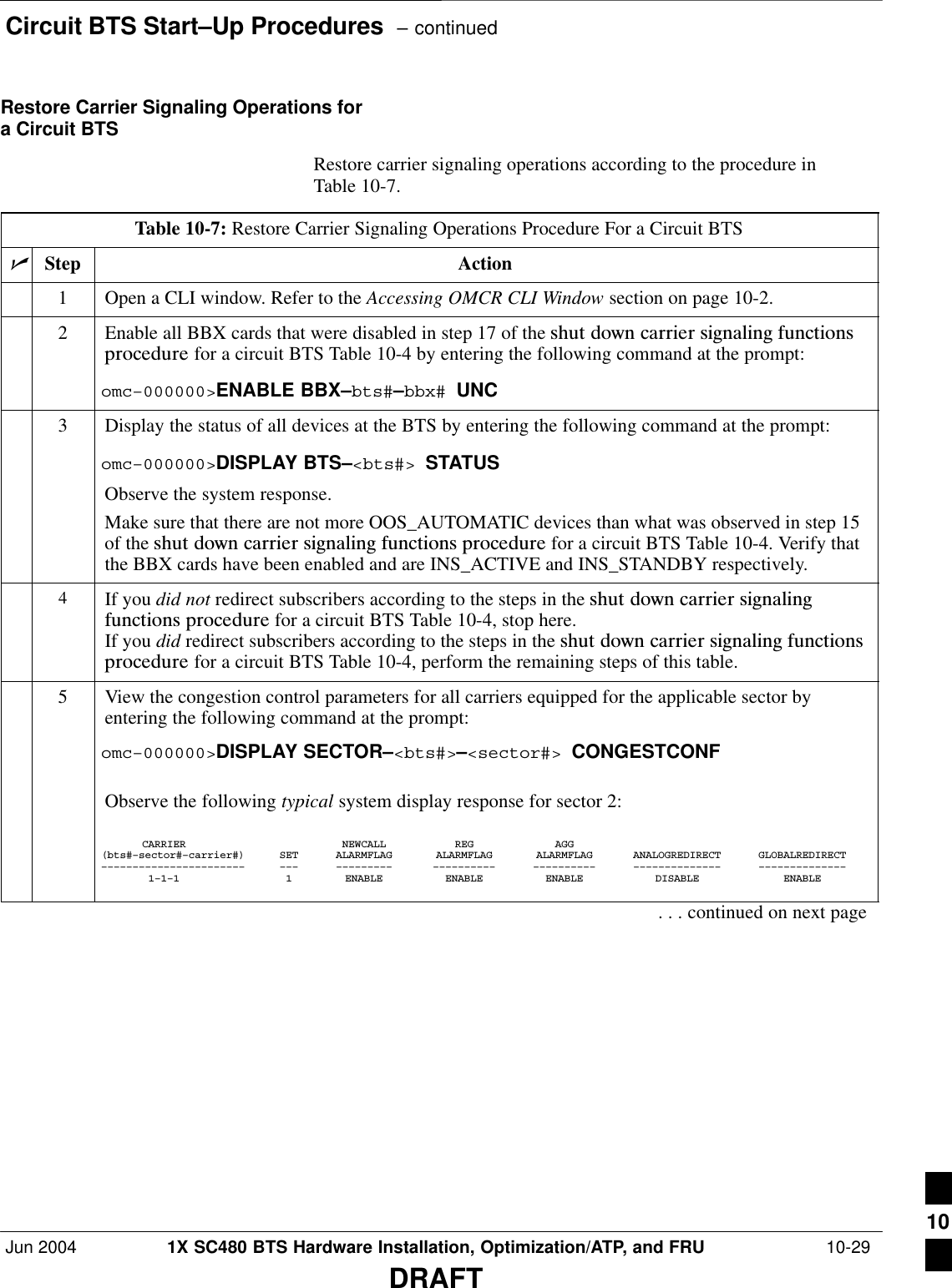
![Circuit BTS Start–Up Procedures – continued 10-30 1X SC480 BTS Hardware Installation, Optimization/ATP, and FRU Jun 2004DRAFTTable 10-7: Restore Carrier Signaling Operations Procedure For a Circuit BTSnActionStepNOTEIn this step, you will change the value of the Global Service Redirection Flag(GLOBALREDIRECT) in the congestion control parameters so that the Global Service RedirectMessage is only broadcast on the sector paging channel of a specific carrier when there is trafficcongestion in the carrier/sector.6Enter the following command at the prompt using one of the applicable carrier number and theapplicable sector number:omc–000000>EDIT CARRIER–<bts#>–<sector#>–<carrier#> CONGESTCONF !The system will prompt you to enter each control parameter value one at a time. Skip through theprompts until you get to the following:<globalredirect> , enter DISABLE (This will revert the Global Service Redirect Message to congestion control.)The system will display the values of the control parameters. Verify that only theGLOBALREDIRECT value changed.omc–000000>Accept [yes/no]?Enter Y to accept the change.Now the Global Service Redirection Message will only be sent over the sector paging channelwhen there is traffic congestion in the carrier/sector.7Repeat step 6 for each remaining sector number disabled in step 14 of the shut down carriersignaling functions procedure for a circuit BTS Table 10-4.8View the status of the carrier signaling redirect parameters to verify the applicable carrier equippedfor the specific sector.omc–000000>DISPLAY CARRIER–<bts#>–<sector#>–<carrier#> REDIRECTObserve that the values in the system display response should match the values input in step 4 ofthe shut down carrier signaling functions procedure for a circuit BTS Table 10-4.Access Overload Class Redirect Flags ROTATECARRIER ID RETURN 0 0 0 0 0 0 0 0 0 0 1 1 1 1 1 1 TIMER RECORD EXP IGNORE SYS(bts–sector–carrier) IF FAIL 0 1 2 3 4 5 6 7 8 9 0 1 2 3 4 5 (SEC) TYPE SID CDMA ORDERING–––––––––––––––––––– ––––––– – – – – – – – – – – – – – – – – ––––– –––– –––– ––– ––––––––CARRIER–146–2–1 N Y Y Y Y Y Y Y Y Y Y Y Y Y Y Y Y 4 2 13 Y CUSTOM9Enter the following command at the prompt:omc–000000>DISPLAY BTS–<bts#> CONGESTCONFObserve the system display response.Verify that the CONGESTCONF globalredirect is disabled for the specific carrier on each theapplicable sectors.. . . continued on next page10](https://usermanual.wiki/Nokia-Solutions-and-Networks/T6EK1.User-Manual-2-of-4/User-Guide-448329-Page-288.png)
![Circuit BTS Start–Up Procedures – continuedJun 2004 1X SC480 BTS Hardware Installation, Optimization/ATP, and FRU 10-31DRAFTTable 10-7: Restore Carrier Signaling Operations Procedure For a Circuit BTSnActionStep* IMPORTANTIn this step, use the values recorded in step 3 of the shut down carrier signaling functionsprocedure for a circuit BTS Table 10-4 to answer the prompts for the EDIT CARRIERREDIRECT command; except for record type enter 2.NOTEThis step shows the entry of initial standard values which is consistent with the original example;except record type must be 2. Your entries may be different.10 Restore the values of all REDIRECT parameters by entering the following command at theprompt:omc–000000>EDIT CARRIER–<bts#>–<sector#>–<carrier#> REDIRECT !The system will prompt you to enter each command parameter one at a time. Answer the promptsin the following order (Note that the following specified values are consistent with the originalexample. Yours may be different):<accolc0> enter N, <accolc1>enter N, ... <accolc15>enter N<returniffail> , enter N<recordtype> , enter 2<expectedsid> , enter 0<ignorecdma> , enter N<sysordering> , enter CUSTOM<rotatetimer> , enter 4The system will display the command that will be sent. Verify the command syntax.omc–000000>Accept [yes/no]?Enter Y to accept the command or N to go back and enter the correct value(s).11 Repeat steps 5 and 10, as required, for each remaining sector number disabled in step 14 of theshut down carrier signaling functions procedure for a circuit BTS Table 10-4.12 View the status of the signaling REDIRECT parameters by entering the following command at theprompt:omc–000000>DISPLAY BTS–<bts#> REDIRECTEnsure that the values in the system display response match the values for the specific carrier oneach the applicable sector(s) input by the operator in step 10 (see example below). Access Overload Class Redirect Flags RETURN ROTATE RECORD EXP IGNORE SYS CARRIER ID IF FAIL 0 0 0 0 0 0 0 0 0 0 1 1 1 1 1 1 TIMER TYPE SID CDMA ORDERING(bts–sector–carrier) 0 1 2 3 4 5 6 7 8 9 0 1 2 3 4 5 (sec)–––––––––––––––––––– ––––––– – – – – – – – – – – – – – – – – –––––– –––––– ––––– –––––– –––––––– CARRIER–1–1–1 N N N N N N N N N N N N N N N N N 4 2 0 N CUSTOM 10](https://usermanual.wiki/Nokia-Solutions-and-Networks/T6EK1.User-Manual-2-of-4/User-Guide-448329-Page-289.png)
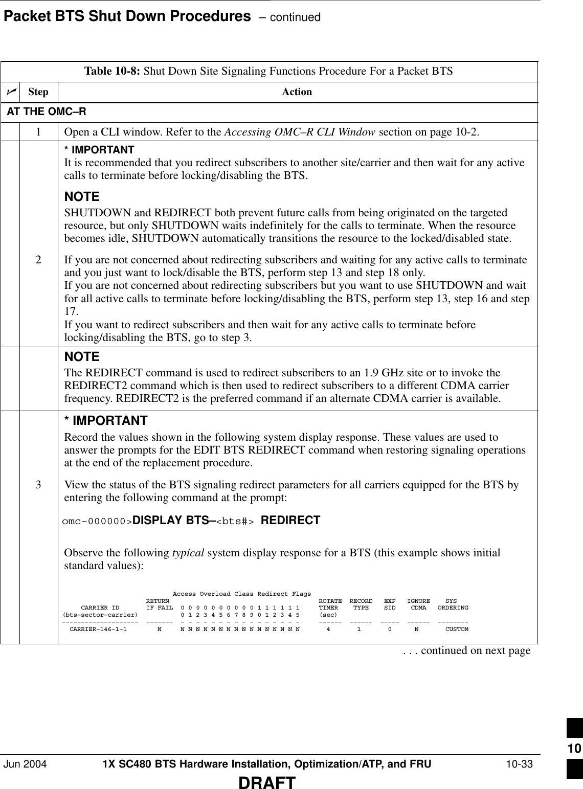
![Packet BTS Shut Down Procedures – continued 10-34 1X SC480 BTS Hardware Installation, Optimization/ATP, and FRU Jun 2004DRAFTTable 10-8: Shut Down Site Signaling Functions Procedure For a Packet BTSnActionStepNOTEThis step edits the REDIRECT parameters so that the Global Service Redirect Message to bebroadcast on the paging channel redirects all subscribers away from the BTS and onto a differentBTS or system.4Enter the following command at the prompt:omc–000000>EDIT BTS–<bts#> REDIRECT!The system prompts you to enter each command parameter value one at a time. Answer theprompts in the following order:<accolc0>enter Y, <accolc1>enter Y, ... <accolc15> enter Y (All Access Overload Classes must be set to yes to ensure that all subscribers are redirected.)<returniffail> , enter N(Must be set to no to ensure that subscribers do not return if redirect is unsuccessful.)<recordtype> , enter 1 or 2 (A value of 2 will invoke REDIRECT2 which is used to redirect subscribers to a CDMA channelat a neighbor site. A value of 1 redirects subscribers to an 1.9 GHz site. This example uses 2.)<expectedsid> , enter 13 (Use the Area ID the subscriber units should expect to find on the system where they are beingredirected. This example uses 13. The valid range is 0 – 32767; the default is 0.)<ignorecdma> , enter Y<sysordering> , enter CUSTOM (The system acquisition ordering value tells the mobiles the order to use when attempting toobtain service on the different analog systems. Valid values are: CUSTOM – use custom systemselection; AONLY – try the A system only; BONLY – use the B system only; AFIRST – try the Asystem first. If unsuccessful, try the B system; BFIRST – try the B system first. If unsuccessful,try the A system; AORB – try A or B. If unsuccessful try the alternative system; CUSTOM is thedefault.)<rotatetimer> , enter 4 (Call processing continuously rotates, circular right–shifts, the Y/N values of Access OverloadClass Redirect Flags 0 to 9. Values are shifted one flag at the end of the timer period; then timerre–starts. Valid values are 0–255; 4 is the default.)The system displays the command to be sent. Verify the command syntax.omc–000000>Accept [yes/no]?Enter Y to accept the command or N to go back and enter the correct value(s).. . . continued on next page10](https://usermanual.wiki/Nokia-Solutions-and-Networks/T6EK1.User-Manual-2-of-4/User-Guide-448329-Page-292.png)
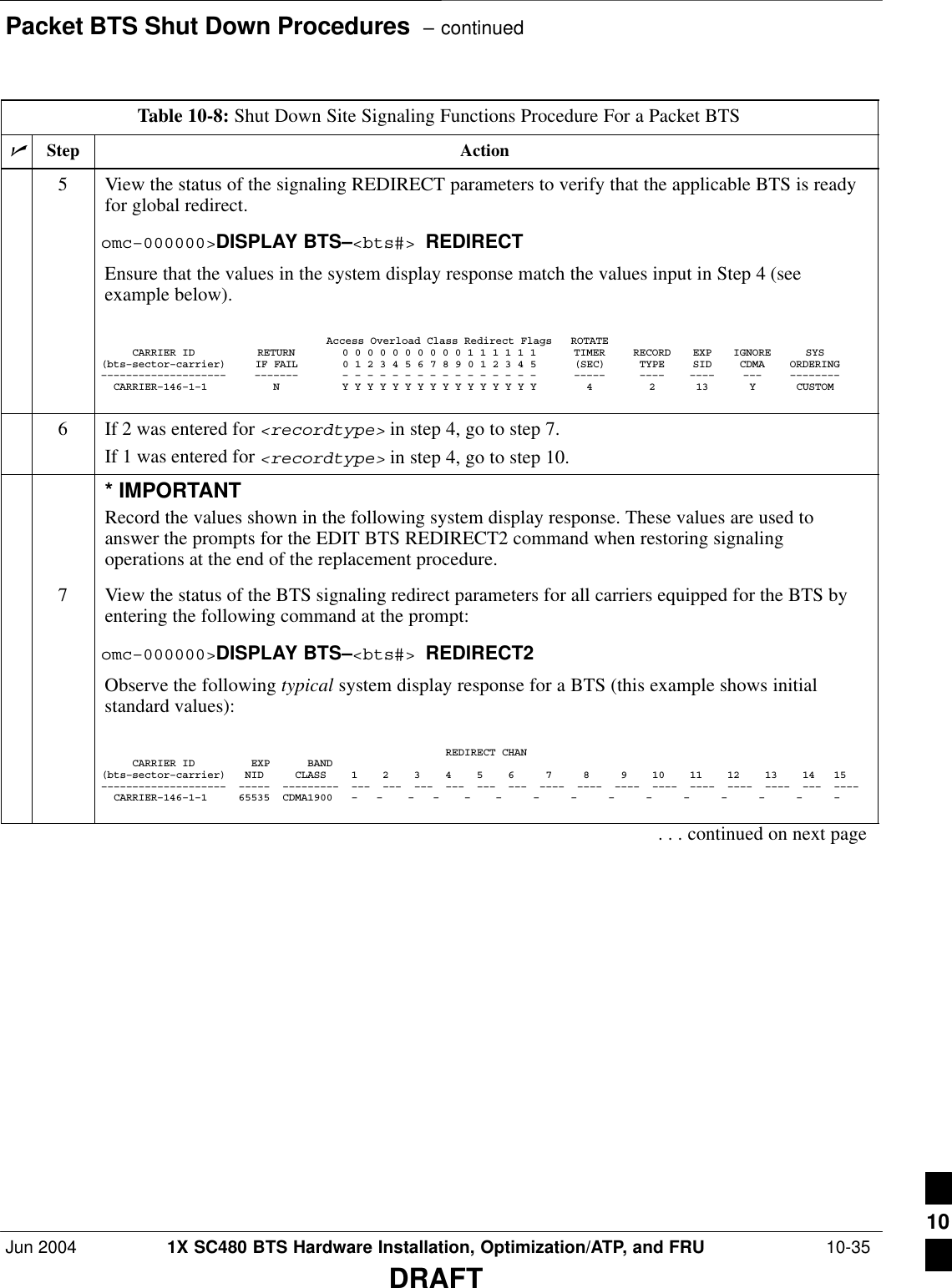
![Packet BTS Shut Down Procedures – continued 10-36 1X SC480 BTS Hardware Installation, Optimization/ATP, and FRU Jun 2004DRAFTTable 10-8: Shut Down Site Signaling Functions Procedure For a Packet BTSnActionStepNOTEThis step edits the REDIRECT2 parameters so that the Global Service Redirect Message to bebroadcast on the paging channel redirects all subscribers away from the BTS with the failedequipment and onto a CDMA channel at a neighbor site.8Enter the following command at the prompt:omc–000000>EDIT BTS–<bts#> REDIRECT2!The system prompts you to enter each command parameter value one at a time. Answer theprompts in the following order:expecting an integer number (from 0 to 65535)<EXPNID= ? >(Use the Network ID the subscriber units should expect to find on the system they are beingredirected to. This example uses 555.)expecting an integer number (from 0 to 2047)<CHAN1= ? >, <CHAN2= ? > ... <CHAN15= ?>(A list of CDMA channels for neighbor sites that the subscriber units can use for redirection. Thisexample uses 200, 350, 400, 725, 75, 175, 100, 575 and 950.)expecting an enumerated value: CDMA1900 CDMA800 CDMA900 JAPANCDMA<BANDCLASS= ? >(Use CDMA1900 for 1.9 GHz systems, and CDMA800 for 800 MHz systems. This example usesCDMA1900.)The system displays the command to be sent. Verify the command syntax.omc–000000>Accept [yes/no]?Enter Y to accept the command or N to go back and enter the correct value(s).9View the status of the BTS signaling REDIRECT2 parameters to verify that the BTS is ready formaintenance.omc–000000>DISPLAY BTS–<bts#> REDIRECT2Ensure that the values in the system display response match the values input in Step 8 (seeexample below). REDIRECT CHAN CARRIER ID EXP BAND(bts–sector–carrier) NID CLASS 1 2 3 4 5 6 7 8 9 10 11 12 13 14 15–––––––––––––––––––– ––––– ––––––––– ––– ––– ––– ––– ––– ––– –––– –––– –––– –––– –––– –––– –––– ––– –––– CARRIER–146–1–1 555 CDMA1900 200 350 400 725 75 175 100 575 950 – – – – – – . . . continued on next page10](https://usermanual.wiki/Nokia-Solutions-and-Networks/T6EK1.User-Manual-2-of-4/User-Guide-448329-Page-294.png)
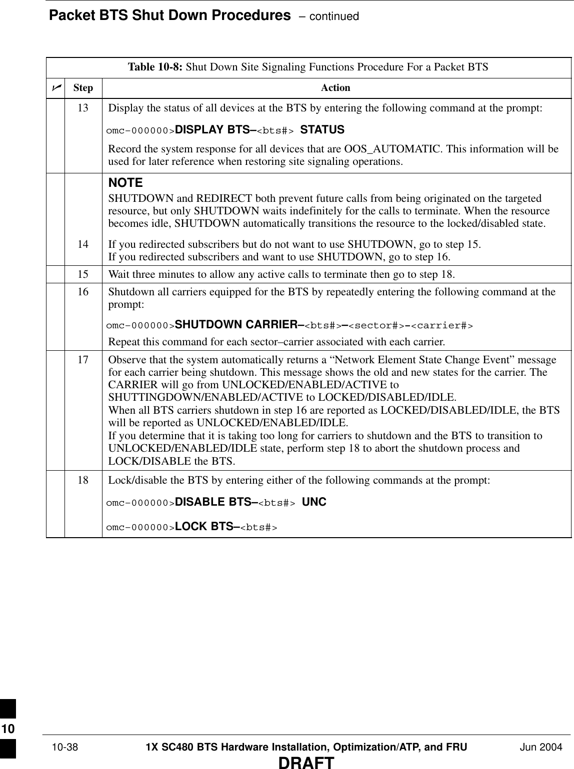
![Packet BTS Shut Down Procedures – continuedJun 2004 1X SC480 BTS Hardware Installation, Optimization/ATP, and FRU 10-37DRAFTTable 10-8: Shut Down Site Signaling Functions Procedure For a Packet BTSnActionStep10 View the existing congestion control parameters for all carriers equipped for the BTS by enteringthe following command at the prompt:omc–000000>DISPLAY BTS–<bts#> CONGESTCONFObserve the following typical system display response for a BTS: CARRIER NEWCALL REG AGG(bts#–sector#–carrier#) SET ALARMFLAG ALARMFLAG ALARMFLAG ANALOGREDIRECT GLOBALREDIRECT––––––––––––––––––––––– ––– ––––––––– ––––––––– ––––––––– –––––––––––––– –––––––––––––– 146–1–1 1 ENABLE ENABLE ENABLE DISABLE DISABLE NOTEIn this step, you will change the value of the Global Service Redirection Flag(GLOBALREDIRECT) in the congestion control parameters so that the Global Service RedirectMessage is broadcast on all of the sector paging channels at the BTS.11 Enter the following command at the prompt using the applicable BTS number:omc–000000>EDIT BTS –<bts#> CONGESTCONF !The system prompts you to enter each control parameter value one at a time. Skip through theprompts until you get to the following:<globalredirect> , enter ENABLE (This will force the Global Service Redirect Message to be broadcast on all of the sector pagingchannels at the BTS.)The system displays the values of the control parameters. Verify that only theGLOBALREDIRECT value changed.omc–000000>Accept [yes/no]?Enter Y to accept the change.Now the Global Service Redirection Message is sent over the sector paging channels. Allsubscribers are redirected away from the BTS and onto a different system or CDMA carrierchannel. This effectively shuts down the BTS.12 Verify that the CONGESTCONF globalredirect is enabled for each carrier at the BTS byentering the following command at the prompt:omc–000000>DISPLAY BTS–<bts#> CONGESTCONFObserve the following typical system display response for a BTS: CARRIER NEWCALL REG AGG(bts#–sector#–carrier#) SET ALARMFLAG ALARMFLAG ALARMFLAG ANALOGREDIRECT GLOBALREDIRECT––––––––––––––––––––––– ––– ––––––––– ––––––––– ––––––––– –––––––––––––– –––––––––––––– 146–1–1 1 ENABLE ENABLE ENABLE DISABLE ENABLE . . . continued on next page10](https://usermanual.wiki/Nokia-Solutions-and-Networks/T6EK1.User-Manual-2-of-4/User-Guide-448329-Page-295.png)
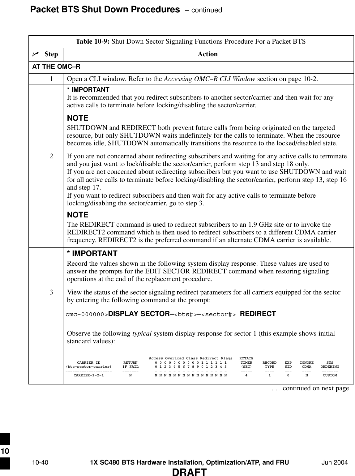
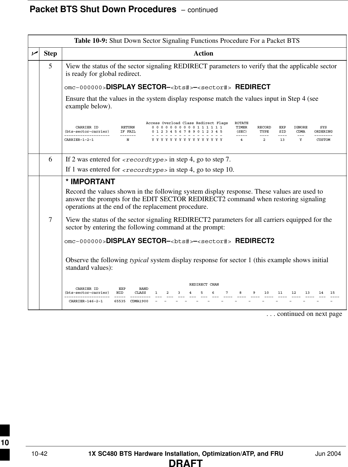
![Packet BTS Shut Down Procedures – continuedJun 2004 1X SC480 BTS Hardware Installation, Optimization/ATP, and FRU 10-41DRAFTTable 10-9: Shut Down Sector Signaling Functions Procedure For a Packet BTSnActionStepNOTEThis step edits the REDIRECT parameters so that the Global Service Redirect Message to bebroadcast on the paging channel redirects all subscribers away from the sector with the failedequipment and onto a different sector, BTS, or system.4Enter the following command at the prompt:omc–000000>EDIT SECTOR–<bts#>–<sector#> REDIRECT !The system prompts you to enter each command parameter value one at a time. Answer theprompts in the following order:<accolc0>enter Y, <accolc1>enter Y,... <accolc15>enter Y(All Access Overload Classes must be set to yes to ensure that all subscribers are redirected.)<returniffail> , enter N(Must be set to no to ensure that subscribers do not return if redirect is unsuccessful.)<recordtype> , enter 1 or 2 (A value of 2 will invoke REDIRECT2 which is used to redirect subscribers to a CDMA channelat a neighbor sector/site. A value of 1 redirects subscribers to an 1.9 GHz site. This example uses2.)<expectedsid> , enter 13 (Use the Area ID the subscriber units should expect to find on the system where they are beingredirected. This example uses 13. The valid range is 0 – 32767; the default is 0.)<ignorecdma> , enter Y<sysordering> , enter CUSTOM (The system acquisition ordering value tells the mobiles the order to use when attempting toobtain service on the different analog systems. Valid values are: CUSTOM – use custom systemselection; AONLY – try the A system only; BONLY – use the B system only; AFIRST – try the Asystem first. If unsuccessful, try the B system; BFIRST – try the B system first. If unsuccessful,try the A system; AORB – try A or B. If unsuccessful try the alternative system; CUSTOM is thedefault.)<rotatetimer> , enter 4 (Call processing continuously rotates, circular right–shifts, the Y/N values of Access OverloadClass Redirect Flags 0 to 9. Values are shifted one flag at the end of the timer period; then timerre–starts. Valid values are 0–255; 4 is the default.)The system displays the command to be sent. Verify the command syntax.omc–000000>Accept [yes/no]?Enter Y to accept the command or N to go back and enter the correct value(s).. . . continued on next page10](https://usermanual.wiki/Nokia-Solutions-and-Networks/T6EK1.User-Manual-2-of-4/User-Guide-448329-Page-299.png)