Nokia Solutions and Networks T6EK1 1X-EVDO SC480 BTS Microcell Base Station Transmtr User Manual print instructions
Nokia Solutions and Networks 1X-EVDO SC480 BTS Microcell Base Station Transmtr print instructions
Contents
- 1. User Manual Part 1 of 4
- 2. User Manual 2 of 4
- 3. User Manual 3 of 4
- 4. User Manual 4 of 4
User Manual 2 of 4
Span Line, RGPS, and RF–GPS Cabling – continued
Jun 2004 4-67
1X SC480 BTS Hardware Installation, Optimization/ATP, and FRU
DRAFT
Connecting Customer–Defined
Inputs to the CBIO
The unit provides eight customer–defined inputs for connection to
external contacts. Each input (a signal/ground pair) is monitored for an
“OPEN” (>50 k Ohms) or “CLOSED” (<3 Ohms) condition.
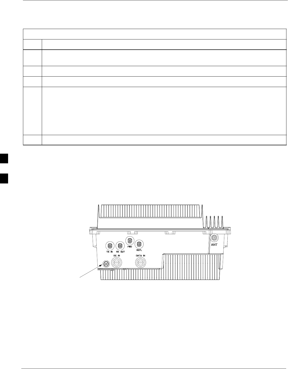
RGPS or RF–GPS Installation
If RGPS is being installed, proceed to Table 4-36. If RF–GPS is being
installed, proceed to Table 3-7.
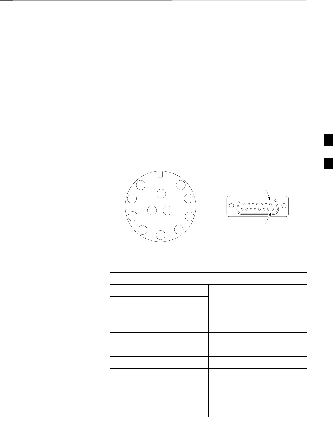
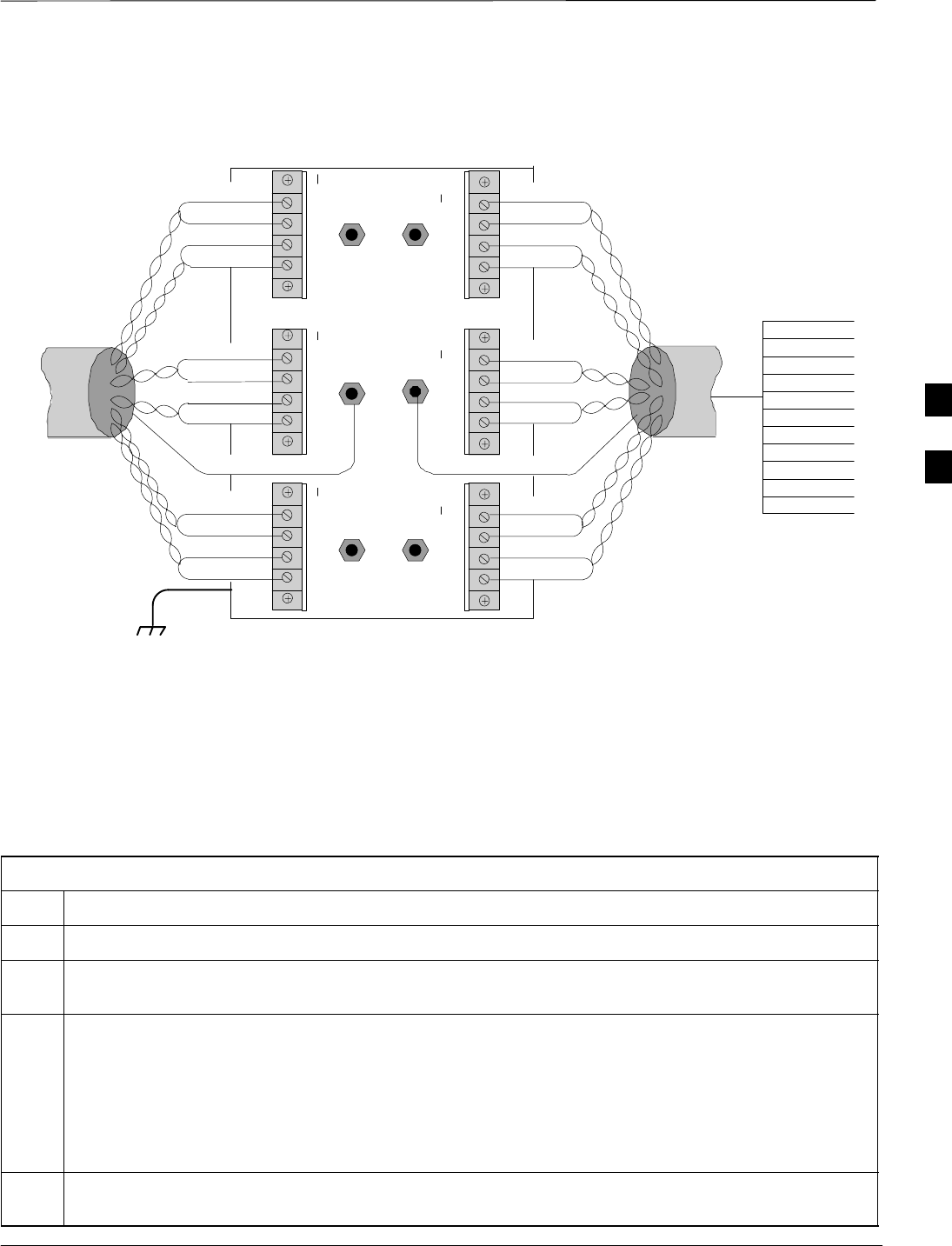
Cable Pinout
Figure 4-42 shows the connector pins on cables C and C1. Table 4-35
gives the pinout for cable C and C1.
Figure 4-42: Connector Pins Numbering for Cables C and C1
1
2
3
456
7
8
9
10
11 12
CONNECTOR FOR
CABLE C
PIN 1
CONNECTOR FOR
CABLE C1
PIN 9
Table 4-35: Pinout for Cables C and C1
Cable C Wire Color Cable C1
Pin Signal Pin
9DC Ground 1 Blue–Black 15
1Power 1 Blue 8
8DC Ground 2 Yellow–Black 14
10 Power 2 Yellow 7
4Transmit Port (–) Green–Black 9
5Transmit Port (+) Green 1
2Receive Port (–) White–Black 12
3Receive Port (+) White 4
7No Connect Red–Black No Connect
table continued on next page
4
Span Line, RGPS, and RF–GPS Cabling – continued
DRAFT
1X SC480 BTS Hardware Installation, Optimization/ATP, and FRU Jun 2004
4-68
Table 4-35: Pinout for Cables C and C1
Cable C Cable C1Wire Color
Pin PinSignal
6No Connect Red No Connect
12 PPS Timing (–) Brown–Black 10
11 PPS Timing (+) Brown 2
Wire colors are the same for both cables.
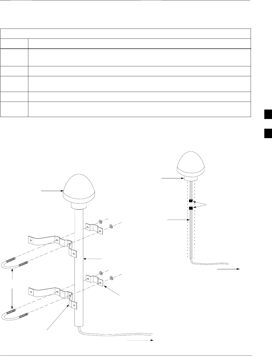
Procedure to Install the RGPS
Head
The RGPS is connected to the BTS via the RGPS connector on the
CBIO Board. See Figure 4-41.
Site specific characteristics determine the GPS cabling that is installed.
Install each cable by referring to the cabling diagram in Figure 4-41, and
the procedure in Table 4-36. The lightning arrestor connections are
shown in Figure 4-46.
Figure 4-43 and Figure 4-44 show the RGPS head. Be sure to factor in
mounting considerations as described in Chapter 3.
The RGPS head must not make contact with any metal
surface other than the provided hardware. Use only the
equipment provided to mount the RGPS head. Failure to
do so could damage the RGPS head.
CAUTION
Table 4-36: Procedure for Installing the RGPS Head and Cabling
Step Action
1Determine the mounting location.
2n WARNING
The structure of the wall should be verified by a qualified structural engineer.
Mounting the RGPS head and hardware to an inadequate wall structure and/or using inadequate
installment methods can result in serious personal injury.
Use the appropriate mounting bolts for the mounting surface and install the two wall mounting
brackets. Refer to Figure 4-43.
3Remove RF–GPS cover plate from CBIO Board.
Remove protective connector cover.
4Connect cables C and C1 into the punch block, as if they were part of the same cable, cut in the
middle maintaining color code and signal integrity. Connect the same corresponding color on both
sides of the punchblock (see Figure 4-41 and Table 4-35).
4
Span Line, RGPS, and RF–GPS Cabling – continued
Jun 2004 4-69
1X SC480 BTS Hardware Installation, Optimization/ATP, and FRU
DRAFT
Table 4-36: Procedure for Installing the RGPS Head and Cabling
Step Action
5Connect RGPS cable (cable C1) to D–connector.
Attach ferrite bead on the cable close to the BTS connector.
6Route RGPS cable C (12–pin Deutsch connector) into the pipe.
7Mate the 12–pin Deutsch connector of the RGPS Head cable and cable C. Refer to Figure 4-43.
Tighten the spinning flange on the connector a quarter turn to secure the connection.
8Insert the pipe into the threaded mount in the RGPS Head and carefully hand–tighten.
9Place the assembly into the mounting brackets. Refer to Figure 4-43. Tighten the U–bolt clamps
to secure the assembly.
Figure 4-43: Installing the Remote GPS Head
WALL MOUNTING
BRACKETS (2)
CLAMP BRACKETS (2)
U–BOLTS
CABLE TO PUNCHBLOCK
(CABLE C)
REFER TO VIEW A
RGPS HEAD WITH
12 PIN MALE
CONNECTOR
MATING
CONNECTORS
RGPS INTERFACE
CABLE WITH 12 PIN
FEMALE CONNECTOR
ON ONE END AND
UNTERMINATED WIRE
ON OTHER END
VIEW A
RGPS HEAD
(MOTOROLA PART
NUMBER 0186012H03)1
NOTE:
1. REPLACEMENT RGPS HEAD
(MOTOROLA PART NUMBER
0186012H04)
CABLE TO PUNCHBLOCK
(CABLE C)
4
Span Line, RGPS, and RF–GPS Cabling – continued
DRAFT
1X SC480 BTS Hardware Installation, Optimization/ATP, and FRU Jun 2004
4-70
Figure 4-44: RGPS Head
THREADED MOUNT ADAPTER
12–PIN DEUTSCH TYPE MMP
CONNECTOR
Connecting the RGPS Cable to
Lightning Arrestor
Figure 4-45 is a detail of the RGPS connections. Figure 4-46 is a detail
of the Lightning Arrestor connections.
Figure 4-45: RGPS to SC480 Connection Diagram
Blue/Black
Blue
Yellow/Black
Yellow
Green/Black
Green
White/Black
White
Red/Black
Red Brown/Black
Brown
1
2
3
45
6
7
8
9
10
11 12
Earth Ground
RGPS CABLE CONNECTOR
(VIEWED FROM CABLE PERSPECTIVE)
C
CABLE DRAIN
LIGHTNING ARRESTOR
(WNP CGDSO971017AA1
OR EQUIVALENT)
D–CONNECTOR
TO BTS
CELL SITE
GROUND =
C1
UNUSED 1
14
10
2
4
12
7
8
15
9
RGPS HEAD (MOTOROLA
P/N 0186012H04)
4
Span Line, RGPS, and RF–GPS Cabling – continued
Jun 2004 4-71
1X SC480 BTS Hardware Installation, Optimization/ATP, and FRU
DRAFT
Blue/Black
Blue
Yellow/Black
Yellow
Green/Black
Green
White/Black
White
Red/Black
Red
Brown/Black
Brown
Cable Drain
Blue/Black
Blue
Yellow/Black
Yellow
Green/Black
Green
White/Black
White
Red/Black
Red
Brown/Black
Brown
Cable Drain
+40VDC Lines +17VDC Lines +17VDC Lines
+17VDC Equipment+17VDC Equipment+40VDC Equipment
C1 (RGPS)
TO BTS
UNIT
C (RGPS)
TO RGPS
RECEIVER
EARTH GROUND MOUNTING PLATE
Blue/Black
Blue
Yellow/Black
Yellow
Green/Black
Green
White/Black
White
Red/Black
Red
Brown/Black
Brown
1
2
3
4
5
6
7
8
9
10
11
12
Figure 4-46: RGPS Lightning Arrestor Wiring
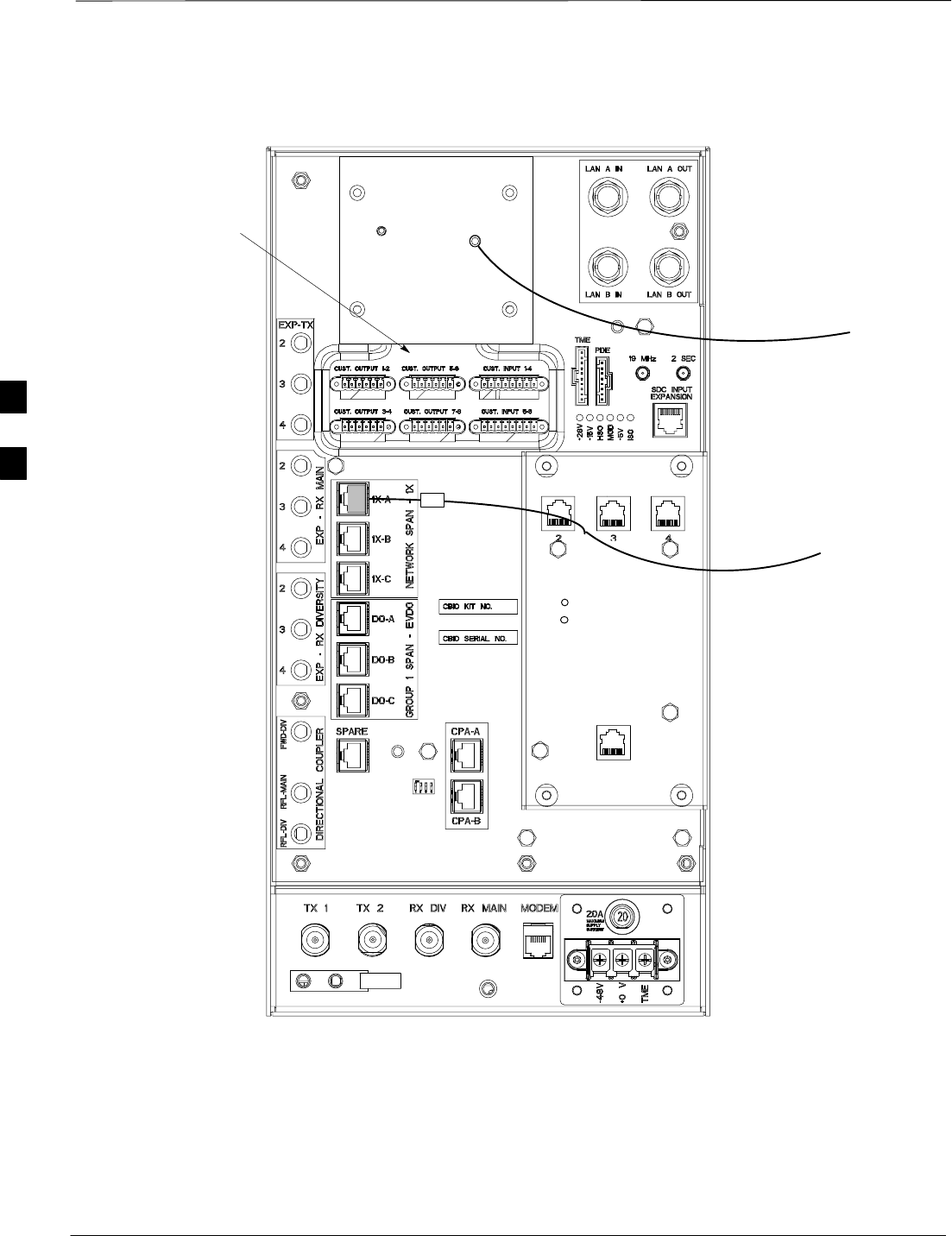
Connecting the RF–GPS Cable
Figure 4-47 shows the components of the RF–GPS. The RF–GPS is
connected to the BTS via the RF–GPS module through the RGPS
connector on the CBIO Board. See Figure 4-48.
Procedure
Use the procedure in Table 4-37 to install the RF–GPS system.
Table 4-37: Procedure for Installing RF–GPS Antenna and Cabling
Step Action
1Determine the mounting location (see RF–GPS Mounting Considerations, Table 6-34).
2Install the mounting kit at the RF–GPS location of choice. Use the appropriate mounting bolts for
mounting surface.
3n WARNING
The roof structure on which the mounting pole is attached should be verified by a qualified structural
engineer for the weight of the RF–GPS engine and mounting hardware or under adverse conditions for
the installation area
Mounting the RF–GPS antenna and hardware to an inadequate roof surface and/or using inadequate
installation methods can result in serious injury.
4Attach the RF–GPS head assembly to the post mounting assembly and secure the assembly to the
assembly to the mounting kit using the screws and nuts supplied (see Figure 4-47).
4

Span Line, RGPS, and RF–GPS Cabling – continued
DRAFT
1X SC480 BTS Hardware Installation, Optimization/ATP, and FRU Jun 2004
4-72
Table 4-37: Procedure for Installing RF–GPS Antenna and Cabling
Step Action
5Attach the grounding kit to the mounting pole.
6Connect one (1) N connector of the 50–feet superflex cable to the N jack of the RF–GPS antenna cable
and route the other end of the cable down to the frame.
7If not already done, attach RF–GPS Module to CBIO Board and secure using 4 M4 screws.
8Route the cable to the RF–GPS connector at the rear of the BTS.
9Connect cable to RF–GPS connector. See Figure 4-48.
4
Span Line, RGPS, and RF–GPS Cabling – continued
Jun 2004 4-73
1X SC480 BTS Hardware Installation, Optimization/ATP, and FRU
DRAFT
FW00410R
4–IN
3/4–IN
3–IN
2”
ANTENNA/PREAMP
(CGDSANT62301)
CABLE ASSEMBLY
(N–DSK) (12–IN LONG)
RUBBER BOOT
(CGDSANT62301)
1/2–IN SCREWS
MOUNTING SHROUD
(CGDSMNT62311)
OUTER GASKET
(CGDSMNT62311)
POST
MOUNTING
ASSEMBLY
(CGDS62312)
CABLE RETAINING NUT
(CGDSMNT62311)
“N” JACK
(CGDSMCXNJACK)
(SEE NOTE 1)
ADJUSTABLE FROM
33.5 TO 47–IN
“N” JACK
CONNECTOR
MOUNTING &
GROUNDING KIT
(CGDS2417071)
(FSJ4–50B) TO BTS
ROOF
NOTE:
1. TOTAL WEIGHT FOR GPS ANTENNA
ASSEMBLY – 0.65 LBS.
REF TO
(CGDSMCXNJACK)
E/K
K
(CGDSVXL550)
Figure 4-47: RF–GPS Installation and Components
4
Span Line, RGPS, and RF–GPS Cabling – continued
DRAFT
1X SC480 BTS Hardware Installation, Optimization/ATP, and FRU Jun 2004
4-74
ti–cdma–wp–00311–v01–ildoc–ah
DAISY–CHAIN SYNC – OUT
SDCX KIT NO.
SDCX SERIAL NO.
DAISY–CHAIN POWER
SDCX POWER
EXPANSION FRAME SYNC – OUT
RF–GPD IN
PWR
J
D
Customer I/O
Figure 4-48: Span and RF–GPS Cabling Details
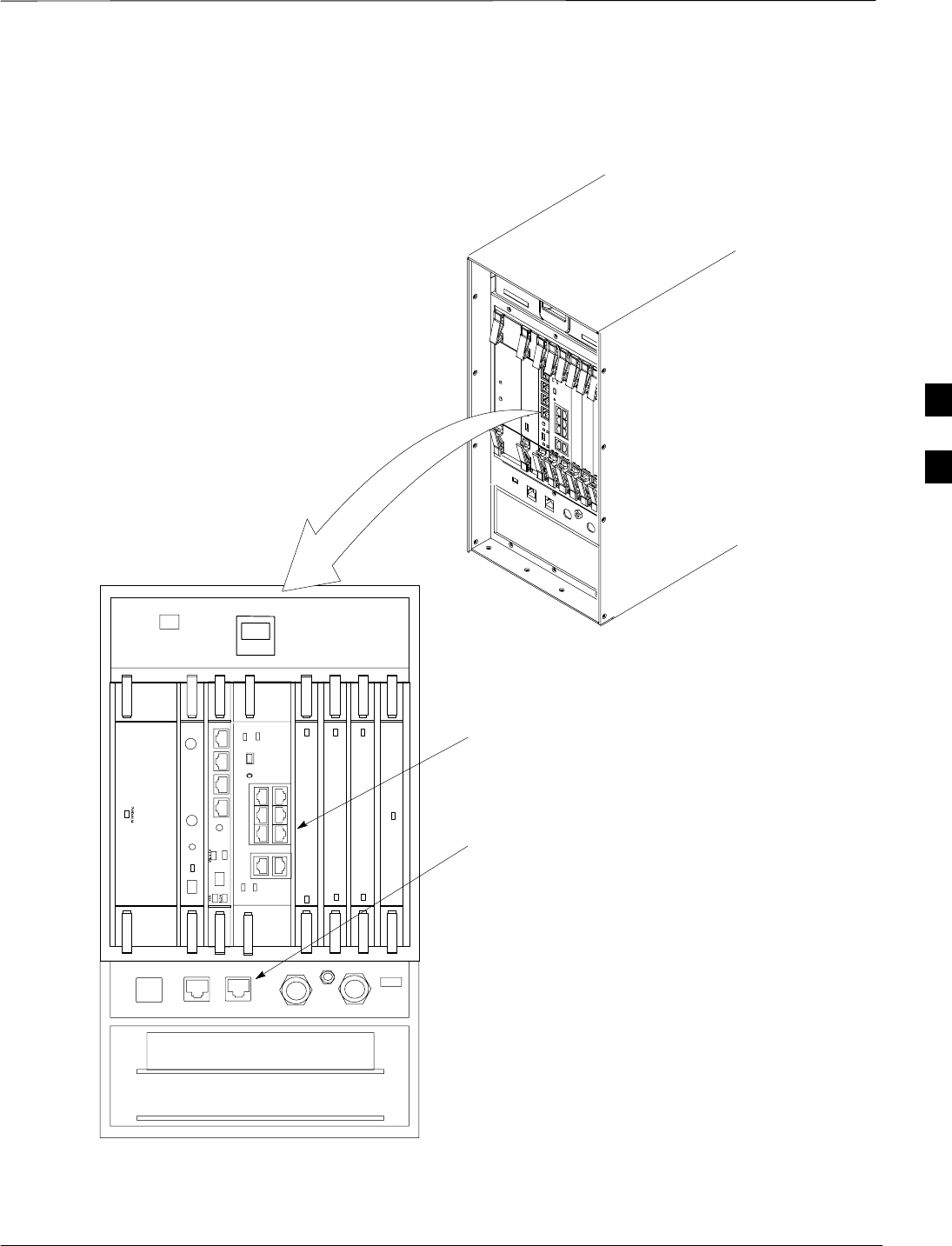
Connecting MCC–DO
At the front of the BTS under the CCP2 Shelf, there are two ethernet
connectors for MCC–DO use: Single and Dual. The connections can be
made with standard ethernet cables. The MCC–DO card provides for
three MCC–DO span lines (See Figure 4-49). Refer to 1X EV–DO
Hardware Installation manual – 68P09257A95 for further information.
4
Span Line, RGPS, and RF–GPS Cabling – continued
Jun 2004 4-75
1X SC480 BTS Hardware Installation, Optimization/ATP, and FRU
DRAFT
ti–cdma–wp–00326–v01–ildoc–ah
Figure 4-49: EV–DO Connections
19MHz EVEN RESET ALARM MMI
PWR/ALM
PWR/ALM
PWR/ALM
PWR/ALM
RESET
GLI
ACTIVE
ACTIVE
ACTIVE
BPR A BPR B AUX
MMI
MMI
GROUP 1 SPAN
DUAL SINGLE LAN A LAN B
SPARE
SYSTEM
STATUS
ENET ENET
ACT
TAT
SINGLE
DUAL
GRP1
SPAN GRP2
SPAN GRP3
SPAN
Ethernet Connections
MCC–DO Span Line
Connections
NOTE:
MCC–DO card occupies MCC
slots 1 & 2.
4

Customer Input / Output Cables
DRAFT
1X SC480 BTS Hardware Installation, Optimization/ATP, and FRU Jun 2004
4-76
Introduction
The objective of this procedure is to attach the ferrite core onto the
customer input and output cables.
Cable Descriptions and Part
Numbers
Table 4-38 gives the cable descriptions and part numbers used to install
the Customer I/O connectors.
Table 4-38: Cable Descriptions and Part Numbers
Cable Qty. Part Number Description
E 1 Customer
Supplied Customer Input/Output cable, 0–8 conductor, 18–24 AWG, stranded
wire
4Molex, terminal
plugs, P/N
39352–0106
Connector, 6 pin
2Molex, terminal
plugs, P/N
39352–0108
Connector, 8 pin
3Motorola P/N
7687717T02 Core, Ferrite
1–3 Customer
Supplied Tie–wrap
Customer Input and Output
Connector Pinouts
Input Pinouts
Table 4-39 lists the pinouts for the Customer Input connectors.
Table 4-39: Customer Input Connector Pinouts
Pin Number Description
1Customer Input 1/5
2Customer Input 1/5 Return
3Customer Input 2/6
4Customer Input 2/6 Return
5Customer Input 3/7
6Customer Input 3/7 Return
table continued on next page
4

Site Cleanup – continued
Jun 2004 4-77
1X SC480 BTS Hardware Installation, Optimization/ATP, and FRU
DRAFT
Table 4-39: Customer Input Connector Pinouts
Pin Number Description
7Customer Input 4/8
8Customer Input 4/8 Return
Output Pinouts
Table 4-40 lists the pinouts for the Customer Output connectors.
Table 4-40: Customer Input Connector Pinouts
Pin Number Description
1Customer Output 1/3/5/7 NC
2Customer Output 1/3/5/7 C
3Customer Output 1/3/5/7 NO
4Customer Output 2/4/6/8 NC
5Customer Output 2/4/6/8 C
6Customer Output 2/4/6/8 NO
Procedure
Follow the procedure in Table 4-41 to attach a ferrite core.
Table 4-41: Procedure for Using Ferrite Core on Customer Input and Output Wires
Step Action
1Route Customer I/O cables from termination equipment to rear of BTS and connect.
2At the rear of the BTS, just below the top, are three pairs of connectors for customer defined inputs
and outputs. See Figure 4-48.
3Connect the cable for Customer Outputs 1 and 2 to BTS connector CUST. OUTPUT 1–2.
Perform the same for the remaining connectors.
4After connections are made, bundle the wires of CUST. OUTPUT 1–2 and CUST. OUTPUT 3–4
together and place a ferrite core around them. Ensure that the wires will not be pinched prior to
closing and latching the ferrite core.
5Slide ferrite core as close to the BTS connectors as possible without causing stress. Use a tie–wrap on
the ferrite core side away from the BTS connectors to hold the ferrite core in place.
6Perform step 4 and step 5 for CUST. OUTPUT 5–6 and CUST. OUTPUT 7–8 and CUST. INPUT
1–4 and CUST. INPUT 5–8.
4

Site Cleanup
DRAFT
1X SC480 BTS Hardware Installation, Optimization/ATP, and FRU Jun 2004
4-78
Remove Protective Covering
Remove any anti–static plastic or cloth sheeting that was used to cover
the equipment.
Lighting Fixtures
Remove the masking tape from the fluorescent light fixtures.
Tools
Place all hand and power tools in the installation tool kit or other
appropriate place. Note any tools that need replacement, cleaning, or
adjustment.
Materials
Place any leftover materials in a location specified by the site manager.
Remove Debris
Remove any packing material.
Ensure that all scrap materials have been removed from any tables or
stands.
Clean/sweep the area. Ensure that all alignment marks have been
removed.
Environment
Remove any temporary weather protection used for installation.
Check that the power connections are tight.
Organize any items (manuals, materials, etc.) left on site and place them
in a location specified by the site manager.
Check that the unit lock is secure and key is removed.
Verify that cabling is properly secured between unit and enclosures.
4

Installation Completion Checklist
Jun 2004 4-79
1X SC480 BTS Hardware Installation, Optimization/ATP, and FRU
DRAFT
Directions
Fill out the installation completion checklist and make any necessary
copies. You may copy this check sheet as needed.
Indoor Installation Completion
Checklist
Date Hardware Installation Completed: ________________________
Site:_______________________________________________________
Serial Number(s):__________________________
__________________________________________________________
Checklist Completed By:_____________________________________
Checklist Reviewed By:______________________________________
Table 4-42: Indoor Installation Completion Checklist
Status No. Item Notes
1Equipment is not damaged.
2Air flow clearance requirements are met.
3Mounting plate is level and secure. (Indoor)
4BTS is securely mounted to plate and rack.
(Indoor)
5TME is securely mounted to wall or pole.
(Outdoor)
6PDM is installed and cabled within TME.
(Outdoor)
7BTS is securely mounted within the TME.
(Outdoor)
8BTS is correctly cabled to TME.
91U Module is installed and cabled to TME (If
used).
10 HMS is securely mounted to TME. (Outdoor)
11 HMS is cabled to TME. (Outdoor)
12 PDE is securely mounted to wall or pole.
(outdoor)
13 HX is securely mounted to PDE. (Outdoor)
14 HX is cabled to PDE. (Outdoor)
15 TME, PDE, and cCLPA are grounded.
(Outdoor)
table continued next page
4

Installation Completion Checklist – continued
DRAFT
1X SC480 BTS Hardware Installation, Optimization/ATP, and FRU Jun 2004
4-80
Table 4-42: Indoor Installation Completion Checklist
Status NotesItemNo.
16 TME is cabled to PDE and cCLPA through
conduit and conduit hubs on TME are tight.
17 PDE is cabled to TME through conduit and
conduit hubs on PDE are tight.
18 cCLPA is cable to TME through conduit and
and conduit hubs on cCLPA are tight.
19 Conduit is sufficiently grounded.
20 200–240 VAC is connected to PDE.
21 Battery backups (if used) are connected to the
PDE.
22 TME DC power cable is connected (through
conduit) to PDE (Outdoor)
23 cCLPA DC power cable is connected through
conduit) to PDE
24 RGPS head and mast are secure.
25 RGPS head has a clear view of the sky and is
not in a location which accumulates debris.
Make sure the RGPS is located away from
the BTS transmit antenna.
26 Local GPS antenna is secure. (If used)
27 Local GPS cabling is installed (If used).
28 Mounting rack is isolated from the Master
ground. (Indoor)
29 cCLPA is securely mounted to rack (if in
use). (Indoor)
30 Compact BTS connection to the DC source is
secure. (Indoor)
31 cCLPA connection to its DC source is secure.
(Indoor)
32 The antenna connections are secure.
33 The antenna cables are protected by lightning
arrestors (if applicable).
34 Span and RGPS connections are protected by
lightning arrestors (if applicable).
35 The RGPS ground lead is connected to the
BTS digital ground reference.
table continued next page
4

Installation Completion Checklist – continued
Jun 2004 4-81
1X SC480 BTS Hardware Installation, Optimization/ATP, and FRU
DRAFT
Table 4-42: Indoor Installation Completion Checklist
Status NotesItemNo.
36 Installation hardware is removed.
37 The earth ground connections are secure
between the earth ground and the Compact
BTS. (Indoor)
38 The DC input cable is securely attached to the
DC input connector. (Indoor)
39 The BTS–to–cCLPA cabling is secure (if
applicable) (Indoor)
40 cCLPA connection to earth ground is secure
(if cCLPA in use). (Indoor)
41 The antenna N–type connectors are securely
attached to the antenna A and B connectors
(if applicable). (Indoor)
42 All unused ports on BTS and/or cCLPA are
properly terminated. (Indoor)
43 All cables are dressed and tied. (Indoor)
44 Power, Span, Customer I/O, PA, RGPS, and
DO cables to the BTS have a ferrite core
attached and tie–wrapped in place.
45 The external power source (DC) is active.
(Indoor)
46 AC power source is active. (Outdoor)
47 The circuit breaker on the BTS is disengaged
(Pulled out).
48 Circuit breakers are disengaged (Pulled out)
on TME PDM. (Outdoor)
49 Circuit breakers are disengaged (Pulled out)
on PDE. (Outdoor)
50 Circuit breaker is disengaged (Pulled out) on
cCLPA.
51 The site is cleaned, swept and trash removed.
52 The site specific documentation is present at
the site.
4

Installation Completion Checklist – continued
DRAFT
1X SC480 BTS Hardware Installation, Optimization/ATP, and FRU Jun 2004
4-82
Notes
4

Jun 2004 1X SC480 BTS Hardware Installation, Optimization/ATP, and FRU
DRAFT
Chapter 5: Power Installation
Table of Contents
Frame Configuration DIP Switch 5-1 . . . . . . . . . . . . . . . . . . . . . . . . . . . . . . . . . . . .
Introduction 5-1 . . . . . . . . . . . . . . . . . . . . . . . . . . . . . . . . . . . . . . . . . . . . . .
Setting Frame Configuration DIP Switch 5-1 . . . . . . . . . . . . . . . . . . . . . . .
Expansion Frame DIP Switch Settings 5-2 . . . . . . . . . . . . . . . . . . . . . . . . .
Expansion 1 Frame DIP Switch 5-3 . . . . . . . . . . . . . . . . . . . . . . . . . . . . . . .
Expansion 2 Frame DIP Switch 5-3 . . . . . . . . . . . . . . . . . . . . . . . . . . . . . . .
Expansion 3 Frame DIP Switch 5-3 . . . . . . . . . . . . . . . . . . . . . . . . . . . . . . .
Pre–Power Up Test (Indoor) 5-4 . . . . . . . . . . . . . . . . . . . . . . . . . . . . . . . . . . . . . . . .
Objective 5-4 . . . . . . . . . . . . . . . . . . . . . . . . . . . . . . . . . . . . . . . . . . . . . . . .
Power for EV–DO 5-4 . . . . . . . . . . . . . . . . . . . . . . . . . . . . . . . . . . . . . . . . .
Test Equipment 5-4 . . . . . . . . . . . . . . . . . . . . . . . . . . . . . . . . . . . . . . . . . . .
Cabling Inspection 5-4 . . . . . . . . . . . . . . . . . . . . . . . . . . . . . . . . . . . . . . . . .
DC Power Pre–Test 5-4 . . . . . . . . . . . . . . . . . . . . . . . . . . . . . . . . . . . . . . . .
cCLPA DC Power Pre–Test 5-5 . . . . . . . . . . . . . . . . . . . . . . . . . . . . . . . . . .
AC Power Input (Outdoor Configuration) 5-7 . . . . . . . . . . . . . . . . . . . . . . . . . . . . .
Objective 5-7 . . . . . . . . . . . . . . . . . . . . . . . . . . . . . . . . . . . . . . . . . . . . . . . .
Test Equipment 5-7 . . . . . . . . . . . . . . . . . . . . . . . . . . . . . . . . . . . . . . . . . . .
Cabling Inspection 5-7 . . . . . . . . . . . . . . . . . . . . . . . . . . . . . . . . . . . . . . . . .
Battery Backup DC Power Input (Outdoor Configuration) 5-9 . . . . . . . . . . . . . . . .
Objective 5-9 . . . . . . . . . . . . . . . . . . . . . . . . . . . . . . . . . . . . . . . . . . . . . . . .
Cable Descriptions and Part Numbers 5-9 . . . . . . . . . . . . . . . . . . . . . . . . . .
Test Equipment 5-9 . . . . . . . . . . . . . . . . . . . . . . . . . . . . . . . . . . . . . . . . . . .
Tools Required 5-9 . . . . . . . . . . . . . . . . . . . . . . . . . . . . . . . . . . . . . . . . . . . .
Cabling Inspection 5-9 . . . . . . . . . . . . . . . . . . . . . . . . . . . . . . . . . . . . . . . . .
Initial Power–Up Test 5-11 . . . . . . . . . . . . . . . . . . . . . . . . . . . . . . . . . . . . . . . . . . . . .
Initial Power–Up Tests 5-11 . . . . . . . . . . . . . . . . . . . . . . . . . . . . . . . . . . . . .
Outdoor Configuration Initial Power Test 5-12 . . . . . . . . . . . . . . . . . . . . . . .
Remove Power 5-14 . . . . . . . . . . . . . . . . . . . . . . . . . . . . . . . . . . . . . . . . . . . . . . . . . .
Removing BTS Power 5-14 . . . . . . . . . . . . . . . . . . . . . . . . . . . . . . . . . . . . . .
Removing cCLPA Power 5-14 . . . . . . . . . . . . . . . . . . . . . . . . . . . . . . . . . . . .
Removing PDE Power 5-14 . . . . . . . . . . . . . . . . . . . . . . . . . . . . . . . . . . . . . .
5

Table of Contents – continued
1X SC480 BTS Hardware Installation, Optimization/ATP, and FRU Jun 2004
DRAFT
Notes
5
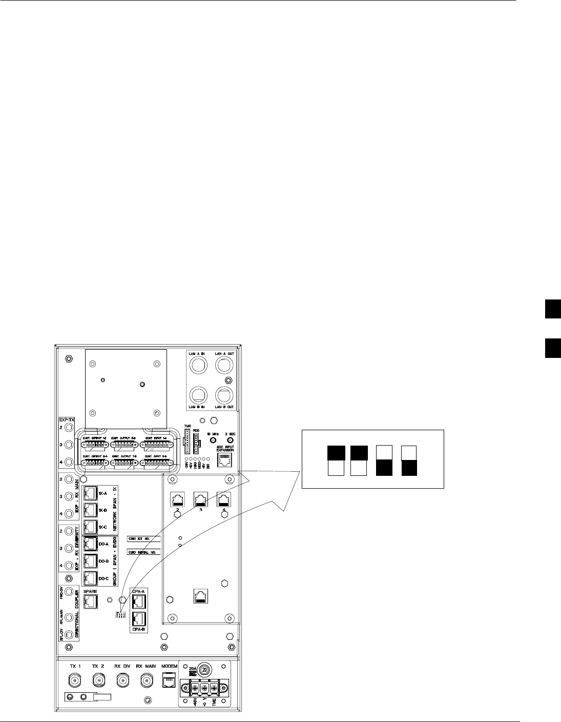
Frame Configuration DIP Switch
Jun 2004 1X SC480 BTS Hardware Installation, Optimization/ATP, and FRU 5-1
DRAFT
Introduction
This section describes setting the DIP switch positions for starter/single
frame and exapansion frames. The following sections describe BTS
preparation before applying DC power.
Setting Frame Configuration
DIP Switch
The frame configuration switch is located on the Compact BTS
Input/Output (CBIO) Card of the BTS. Figure 5-1 shows the switch
position for a starter /single frame configuration. If there are expansion
frames, then each would have the DIP switch positions set to reflect that
frames identification. See Figure 5-2.
The switch settings must be verified and set before power is applied to
the BTS. Refer to Figure 5-1 or Table 5-1 for a starter or single frame.
Figure 5-1: DIP Switch Configuration
Frame ID
3rd and 4th Positions
– Don’t Care
1 2 3 4
DN
Note:
Black represents Switch Actuator
UP
DAISY–CHAIN SYNC – OUT
SDCX
KIT NO.
SDCX
SERIAL NO.
DAISY–CHAIN
POWER
SDCX POWER
EXPANSION FRAME SYNC – OUT
RF–GPS IN
PWR
5
Frame Configuration DIP Switch – continued
5-2 1X SC480 BTS Hardware Installation, Optimization/ATP, and FRU Jun 2004
DRAFT
Table 5-1: Frame ID Switch Position – Single/Starter Frame
1 2 3 4
UP UP –– ––
–– = Don’t Care. These switch positions do not affect the BTS.
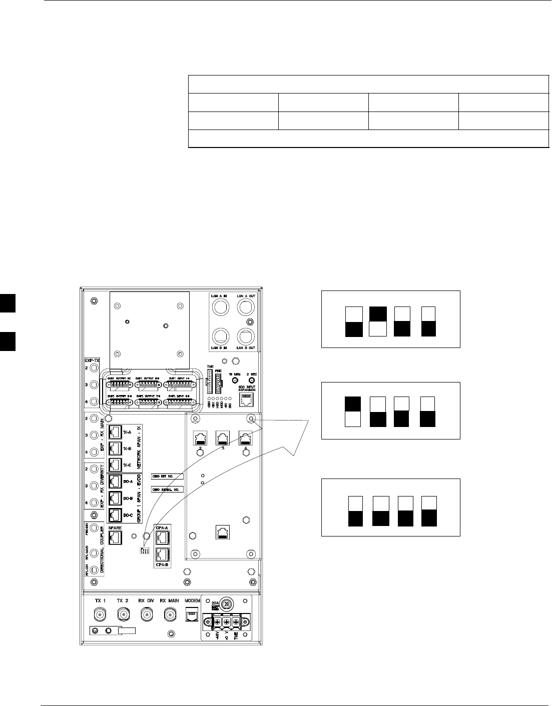
Expansion Frame DIP Switch
Settings
Figure 5-2 shows the switch position for the expansion frames.
Figure 5-2: Expansion Frames DIP Switch Configuration
Expansion 1
3rd and 4th Positions
– Don’t Care
1 2 3 4
DN
Note:
Black represents Switch Actuator
UP
Expansion 2
1 2 3 4
DN
UP
Expansion 3
1 2 3 4
DN
UP
DAISY–CHAIN SYNC – OUT
SDCX
KIT NO.
SDCX
SERIAL NO.
DAISY–CHAIN
POWER
SDCX POWER
EXPANSION FRAME SYNC – OUT
RF–GPS IN
PWR
5

Frame Configuration DIP Switch – continued
Jun 2004 1X SC480 BTS Hardware Installation, Optimization/ATP, and FRU 5-3
DRAFT
Expansion 1 Frame DIP Switch
The switch settings must be verified and set before power is applied to
the BTS. Refer to Figure 5-2 or Table 5-2 for the expansion 1 frame.
Table 5-2: Frame ID Switch Position – Expansion 1 Frame
1 2 3 4
DN UP –– ––
–– = Don’t Care. These switch positions do not affect the BTS.
Expansion 2 Frame DIP Switch
The switch settings must be verified and set before power is applied to
the BTS. Refer to Figure 5-2 or Table 5-3 for Expansion 2 frame.
Table 5-3: Frame ID Switch Position – Expansion 2 Frame
1 2 3 4
UP DN –– ––
–– = Don’t Care. These switch positions do not affect the BTS.
Expansion 3 Frame DIP Switch
The switch settings must be verified and set before power is applied to
the BTS. Refer to Figure 5-2 or Table 5-4 for Expansion 3 frame.
Table 5-4: Frame ID Switch Position – Expansion 3 Frame
1 2 3 4
DN DN –– ––
–– = Don’t Care. These switch positions do not affect the BTS.
5
Pre–Power Up Test (Indoor)
5-4 1X SC480 BTS Hardware Installation, Optimization/ATP, and FRU Jun 2004
DRAFT
Objective
This procedure check for any electrical problems and verifies the
operation and tolerances of the cell site BTS power supply prior to
applying power for the first time.
Power for EV–DO
Information for applying power to a BTS equipped with EV–DO
(MCC–DO) can be found in 1xEV–DO Hardware Installation manual –
68P09257A95
Test Equipment
The following test equipment is required to perform the Pre–Power Up
test:
SDigital Multimeter (DMM)
Before handling any circuit cards or modules, be sure to
wear a grounding strap to prevent damage from ESD.
CAUTION
Cabling Inspection
Using the site specific documentation generated by Motorola Systems
Engineering, verify that the following cable systems are properly
connected:
SDC Power cabling
SReceive RF cabling
STransmit RF cabling
SGPS
DC Power Pre–Test
Perform the procedure Table 5-5 in before applying any power to the
BTS.
Table 5-5: BTS DC Pre–Power Test
Step Action
* IMPORTANT
When handling circuit boards and modules, be sure to wear a grounding strap to prevent damages
caused by ESD.
1Remove front panel cover.
2Unseat all circuit boards and modules, but do not remove them from their slots.
table continued on next page
5
Pre–Power Up Test (Indoor) – continued
Jun 2004 1X SC480 BTS Hardware Installation, Optimization/ATP, and FRU 5-5
DRAFT
Table 5-5: BTS DC Pre–Power Test
Step Action
3At the rear of the BTS, verify that 20 or 25 A circuit breaker is OFF (pulled out). See Figure 5-3 or
Figure 1-8.
4Use a DMM (set to ohms) and verify the resistance on the +27V bus.
– Remove the Power Supply Module from the CCP2 Shelf
– Verify that the resistance from the power (+) feed terminal with respect to ground measures > 500
W
See Figure 5-3
– Verify that the resistance from the power (–) feed terminal with respect to ground measures > 500
W
See Figure 5-3
– The resistance measurement should not read 0 (zero).
5Re–seat all circuit boards into their slots
6Install the Power Supply Module into its slot.
7Install front panel cover.
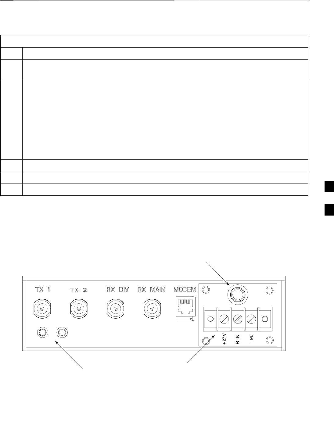
GROUND Location
(Screw Holes)
DC Power
Terminal Strip
Circuit Breaker
25A
Figure 5-3: Location of Circuit Breaker
25
cCLPA DC Power Pre–Test
Perform the procedure Table 5-6 in before applying any power to the
cCLPA.
5
Pre–Power Up Test (Indoor) – continued
5-6 1X SC480 BTS Hardware Installation, Optimization/ATP, and FRU Jun 2004
DRAFT
Table 5-6: cCLPA DC Pre–Power Test
Step Action
1Ensure that DC power is disengaged at the source. Verify that the DC power cable has been connected
using the procedure in Table 4-8.
2Remove I/O panel cover.
3At the bottom of the cCLPA, verify that 25 A circuit breaker to OFF (pulled out). See Figure 5-4.
4Us a DMM (set to ohms) and verify the resistance on the +27 V bus.
– Verify that the resistance from the power (+) feed terminal with respect to ground measures > 500
W
– Verify that the resistance from the power (–) feed terminal with respect to ground measures > 500
W
The resistance measurement should not read 0 (zero).
5Proceed to Initial Power up procedure in Table 5-11.
ti–cdma–wp–00298–v01–ildoc–ah
Figure 5-4: Bottom View of cCLPA
25A FUSE
for +27 V
5

AC Power Input (Outdoor Configuration)
Jun 2004 1X SC480 BTS Hardware Installation, Optimization/ATP, and FRU 5-7
DRAFT
Objective
The objective of this procedure is to verify the AC power for the
Compact BTS outdoor configuration.
Test Equipment
The following test equipment is required to perform the Pre–Power Up
test:
SDigital Multimeter (DMM) or equivalent
Cabling Inspection
Using the site specific documentation generated by Motorola Systems
Engineering, verify that the following cable systems are properly
connected:
SAC Power cabling
SDC Power Cabling
AC power was installed per manufacturer’s installation procedure.
Perform the procedure Table 5-7 in before applying any power to the
TME and cCLPA.
Table 5-7: PDE Initial Power –Up Test
Step Action
* IMPORTANT
To avoid extensive re–work of the PDE and BTS connections, this procedure should be performed
after the PDE and TME are mounted in place.
n WARNING
This equipment uses dangerous voltages and is capable of causing death. Failure to observe this
Warning could result in electrical shock to personnel and damage to equipment. The AC voltage
source should be isolated and locked, and a clearly visible, Warning label attached.
1Verify that AC power from the source is OFF.
2If not already done, remove safety shield covering AC terminal block.
3Connect AC power cable to AC power source.
4Verify that PDE DC circuit breakers are set to “O” or pulled out (disengaged).
5Verify that AC power cable is securely connected to PDE AC terminal block.
6Turn on AC power source.
n WARNING
This equipment uses dangerous voltages and is capable of causing death. Failure to observe this
Warning could result in electrical shock to personnel and damage to equipment. Do not wear jewelry
on hands/fingers when making electrical measurements.
table continued on next page
5

AC Power Input (Outdoor Configuration) – continued
5-8 1X SC480 BTS Hardware Installation, Optimization/ATP, and FRU Jun 2004
DRAFT
Table 5-7: PDE Initial Power –Up Test
Step Action
7Using a DMM set toVAC, measure the voltage at the AC terminal block. DMM should indicate
200–240 VAC. Adjust AC voltage as necessary.
8Remove DMM.
9If there is nothing further to do, replace safety shield. Secure to cabinet with 2 nuts and washers. Use
an adjustable wrench to tighten nuts. Torque nuts to 3.4 N–M (20 in–lbs).
5

Battery Backup DC Power Input (Outdoor Configuration)
Jun 2004 1X SC480 BTS Hardware Installation, Optimization/ATP, and FRU 5-9
DRAFT
Objective
The objective of this procedure is to verify the Battery Backup DC
power for the Compact BTS outdoor configuration.
Cable Descriptions and Part
Numbers
Table 5-8 gives the cable description and part number for the
recommended cable. Consult manufacturer’s installation guide for
further information.
Table 5-8: Cable Descriptions and Part Numbers
Cable Qty. Part Number Description
{L 1 Customer
Supplied DC power cables, 10 AWG, stranded, designed for +20 to +34 VDC
power input
{ Length of cables are dependent upon BTS equipment layout.
Test Equipment
The following test equipment is required to perform the Pre–Power Up
test:
SDigital Multimeter (DMM) or equivalent
Tools Required
Relatively small, flat head, screwdriver or equivalent.
Cabling Inspection
Using the site specific documentation generated by Motorola Systems
Engineering, verify that the following cable systems are properly
connected:
SAC Power cabling
SDC Power Cabling
Battery Backup has been installed per the manufacturer’s installation
procedure.
Following the procedure in Table 5-9 to verify Battery Backup DC
power is present.
Table 5-9: Procedure to Verify Battery Backup DC Power Test
Step Action
n WARNING
Do not wear a grounding device or metal of any kind on hands/fingers when working with voltage.
injury to personnel and damage to equipment could occur.
1Verify that Battery Backup DC Power is disengaged.
table continued on next page
5

Battery Backup DC Power Input (Outdoor Configuration) – continued
5-10 1X SC480 BTS Hardware Installation, Optimization/ATP, and FRU Jun 2004
DRAFT
Table 5-9: Procedure to Verify Battery Backup DC Power Test
Step Action
2If not already done, connect Battery Backup DC power cable to batteries.
3If not already done, remove safety shield covering DC terminal block.
4Verify that Battery Backup DC power cable is securely connected to DC terminal block of PDE.
5Verify that circuit breakers on PDE front panel are disengaged (pulled out or set to “O” (OFF)).
6Turn on Battery Backup source.
7Using a DMM set to VDC, measure the voltage at the DC terminal block. DMM indicates VDC in the
range +20 to +34 VDC.
8Remove DMM.
9If there is nothing further to do, replace safety shield. Secure to cabinet with 2 nuts and washers. Use
an adjustable wrench to tighten nuts. Torque nuts to 3.4 N–M (20 in–lbs).
5
Initial Power–Up Test
Jun 2004 1X SC480 BTS Hardware Installation, Optimization/ATP, and FRU 5-11
DRAFT
Initial Power–Up Tests
Potentially lethal voltage and current levels are present in
the Compact BTS. This test must NOT be performed
without a second person present capable of administering
emergency medical treatment. Remove all decorative metal
before beginning this test. Do NOT wear a grounding strap
when performing voltage measurements.
WARNING
BTS Initial Power–Up
Perform the procedure in Table 5-10 to verify input power. Once power
has been applied the cards and modules within the BTS should begin
operating within specifications.
Table 5-10: Procedure for BTS Initial Power–Up
Step Action
NOTE
If the BTS is being utilized in an outdoor configuration, perform this procedure after the TME has
been verified as operational.
1Ensure that DC power source is OFF.
2Connect DC power to BTS DC Power input.
3Turn on DC power source.
4Use a DMM (set to VDC) to verify the +27 V power output is within +20 to +34 VDC)
5On the BTS, set the 25 A circuit breaker to ON (push in). See Figure 5-3.
6If not already done, install the fan module, note that the fan module begins operating. Feel for air
movement at the exhaust vent on top of the BTS.
7Ensure that all circuit boards and modules are seated and locked into their associated slots.
cCLPA Initial Power –Up
Perform the procedure in Table 5-11 to perform the initial power–up.
Table 5-11: Procedure cCLPA Initial Power–Up
Step Action
NOTE
If the cCLPA is being utilized in an outdoor configuration, perform this procedure after the PDE has
been verified as operational.
1Ensure that DC power source is OFF.
table continued on next page
5

Initial Power–Up Test – continued
5-12 1X SC480 BTS Hardware Installation, Optimization/ATP, and FRU Jun 2004
DRAFT
Table 5-11: Procedure cCLPA Initial Power–Up
Step Action
2 If not already done, remove cCLPA I/O panel cover.
3Connect DC power to cCLPA I/O board DC terminal block.
4Turn on DC power source.
5Using a DMM (set to VDC), measure the voltage at the cCLPA I/O board terminal block.
DC voltage should measure in the range of +20 to +34 VDC. Adjust DC power source as necessary.
6Remove DMM and install I/O panel cover.
7On the cCLPA, push in 20 A circuit breaker.
Outdoor Configuration Initial
Power Test
TME Initial Power–Up
Perform the procedure Table 5-12 in before applying any power to the
BTS and HMS.
Table 5-12: TME DC Initial Power–Up Test
Step Action
* IMPORTANT
To avoid extensive re–work of the TME and BTS connections, this procedure should be performed
after the TME with BTS is mounted in place.
NOTE
Perform this procedure after the PDE has been verified as operational.
1Verify that DC power from the PDE is OFF.
2If not already done, route DC power cable from PDE through conduit to TME.
3If not already done, remove protective cover from voltage connection on PDA.
4Use a Phillips screw driver to remove screws from DC power connector on PDA.
5Set lug of “–” wire in the RTN location and secure with screw.
6Set lug of “+” wire in the +27 VDC location and secure with screw.
7Verify that 1U and TME circuit breakers on PDA are disengaged (pulled out).
8Turn on PDE supplying the TME.
9Using a DMM set to VDC, measure the voltage at the PDA connector. DMM should indicate +20 to
+34 VDC.
10 If not already done, connect PDA to HMS Controller (D–connector)
table continued on next page
5

Initial Power–Up Test – continued
Jun 2004 1X SC480 BTS Hardware Installation, Optimization/ATP, and FRU 5-13
DRAFT
Table 5-12: TME DC Initial Power–Up Test
Step Action
11 If not already done, connect PDA to BTS. (Three appropriately marked cables .)
12 Engage (push in) TME circuit breaker on PDA.
NOTE
Fans on HMS and BTS begin to operate. With TME cable connected the controller for the HMS and
BTS is bypassed, and DC power is supplied as long as the TME circuit breaker is engaged.
13 Using a DMM set to VDC, measure the voltage at the BTS DC Input connector. DMM should indicate
+20 to +34 VDC.
14 Using a DMM set to VDC, measure the voltage at the HMS Controller connector. DMM should
indicate +20 to +34 VDC.
15 If the 1U connector is being used, engage 1U circuit breaker (push in), use a DMM set to VDC to
measure the voltage at the 1U unit connector. DMM should indicate +20 to +34 VDC.
NOTE
If 1U connector is not in use, do not measure at this time.
5

Remove Power
5-14 1X SC480 BTS Hardware Installation, Optimization/ATP, and FRU Jun 2004
DRAFT
Removing BTS Power
Perform the procedure in Table 5-13, if power must be removed from the
BTS.
Table 5-13: Procedure to Remove Power to BTS
Step Action
1For indoor configuration, set the 25 A circuit breaker to OFF (pulled out). See Figure 5-3.
For outdoor configuration, open TME and set circuit breaker on PDA to “O”.
Set TME circuit breaker on PDE to OFF.
2Confirm all LEDs are OFF.
3If possible, for added safety, locate circuit breaker of DC power source (PDE or Battery Backup) and
set it to OFF.
Removing cCLPA Power
Perform the procedure in Table 5-14, if power must be removed from the
cCLPA.
Table 5-14: Procedure to Remove Power to cCLPA
Step Action
1Set the 20A circuit breaker to OFF (pulled out). See Figure 5-4.
2For indoor configuration, turn off DC power source.
For outdoor configuration, pull cCLPA circuit breaker on PDE out.
3Turn off Battery backup DC power (if used).
Removing PDE Power
Perform the procedure in Table 5-15, if power must be removed from the
PDE.
Table 5-15: Procedure to Remove Power to PDE
Step Action
1Turn off AC power source.
2Turn off Battery Backup DC power (if used).
5

Jun 2004 1X SC480 BTS Hardware Installation, Optimization/ATP, and FRU
DRAFT
Chapter 6: Optimization and Calibration
Table of Contents
Preliminary Operations: Overview 6-1 . . . . . . . . . . . . . . . . . . . . . . . . . . . . . . . . . . .
Introduction 6-1 . . . . . . . . . . . . . . . . . . . . . . . . . . . . . . . . . . . . . . . . . . . . . .
Cicruit Backhaul Operation 6-1 . . . . . . . . . . . . . . . . . . . . . . . . . . . . . . . . . .
Packet Backhaul Operation 6-1 . . . . . . . . . . . . . . . . . . . . . . . . . . . . . . . . . .
Cell–site Types 6-1 . . . . . . . . . . . . . . . . . . . . . . . . . . . . . . . . . . . . . . . . . . . .
CDF/NECF 6-1 . . . . . . . . . . . . . . . . . . . . . . . . . . . . . . . . . . . . . . . . . . . . . .
Site Equipage Verification 6-2 . . . . . . . . . . . . . . . . . . . . . . . . . . . . . . . . . . .
Initial Installation of Boards/Modules 6-2 . . . . . . . . . . . . . . . . . . . . . . . . . .
Ethernet LAN 6-3 . . . . . . . . . . . . . . . . . . . . . . . . . . . . . . . . . . . . . . . . . . . . . . . . . . .
Ethernet LAN Termination 6-3 . . . . . . . . . . . . . . . . . . . . . . . . . . . . . . . . . .
Introduction to Optimization and Calibration 6-4 . . . . . . . . . . . . . . . . . . . . . . . . . .
Overview 6-4 . . . . . . . . . . . . . . . . . . . . . . . . . . . . . . . . . . . . . . . . . . . . . . . .
Optimization Process Summary 6-4 . . . . . . . . . . . . . . . . . . . . . . . . . . . . . .
Cell-site Types 6-5 . . . . . . . . . . . . . . . . . . . . . . . . . . . . . . . . . . . . . . . . . . . .
CDF/NECF 6-5 . . . . . . . . . . . . . . . . . . . . . . . . . . . . . . . . . . . . . . . . . . . . . .
BTS System Software Download 6-6 . . . . . . . . . . . . . . . . . . . . . . . . . . . . .
Site Equipage Verification 6-6 . . . . . . . . . . . . . . . . . . . . . . . . . . . . . . . . . . .
Preparing the LMF 6-7 . . . . . . . . . . . . . . . . . . . . . . . . . . . . . . . . . . . . . . . . . . . . . . .
Overview of Packet BTS files 6-7 . . . . . . . . . . . . . . . . . . . . . . . . . . . . . . . .
WinLMF Features and Installation Requirements 6-8 . . . . . . . . . . . . . . . . .
WinLMF File Structure Overview 6-9 . . . . . . . . . . . . . . . . . . . . . . . . . . . . .
WinLMF Home Directory 6-9 . . . . . . . . . . . . . . . . . . . . . . . . . . . . . . . . . . .
NECF Filename Conventions and Directory Location 6-10 . . . . . . . . . . . . .
WinLMF Operating System Installation 6-11 . . . . . . . . . . . . . . . . . . . . . . . .
Copy BTS CDF (or NECF) and CBSC CDF Files to the
WinLMF Computer 6-12 . . . . . . . . . . . . . . . . . . . . . . . . . . . . . . . . . . . . . . . .
Creating a Named HyperTerminal Connection for MMI
Communication 6-14 . . . . . . . . . . . . . . . . . . . . . . . . . . . . . . . . . . . . . . . . . . .
Span Lines – Interface and Isolation 6-16 . . . . . . . . . . . . . . . . . . . . . . . . . . . . . . . . . .
T1/E1 Span Interface 6-16 . . . . . . . . . . . . . . . . . . . . . . . . . . . . . . . . . . . . . . .
Isolate BTS from T1/E1 Spans 6-16 . . . . . . . . . . . . . . . . . . . . . . . . . . . . . . .
T1/E1 Span Isolation 6-16 . . . . . . . . . . . . . . . . . . . . . . . . . . . . . . . . . . . . . . .
LMF to BTS Connection 6-17 . . . . . . . . . . . . . . . . . . . . . . . . . . . . . . . . . . . . . . . . . .
Connect the WinLMF to the BTS 6-17 . . . . . . . . . . . . . . . . . . . . . . . . . . . . .
Using the LMF 6-18 . . . . . . . . . . . . . . . . . . . . . . . . . . . . . . . . . . . . . . . . . . . . . . . . . .
Basic LMF Operation 6-18 . . . . . . . . . . . . . . . . . . . . . . . . . . . . . . . . . . . . . .
6

Table of Contents – continued
1X SC480 BTS Hardware Installation, Optimization/ATP, and FRU Jun 2004
DRAFT
The LMF Display and the BTS 6-19 . . . . . . . . . . . . . . . . . . . . . . . . . . . . . . .
Graphical User Interface Overview 6-19 . . . . . . . . . . . . . . . . . . . . . . . . . . . .
Understanding GUI Operation 6-19 . . . . . . . . . . . . . . . . . . . . . . . . . . . . . . . .
Command Line Interface Overview 6-24 . . . . . . . . . . . . . . . . . . . . . . . . . . . .
Logging Into a BTS 6-25 . . . . . . . . . . . . . . . . . . . . . . . . . . . . . . . . . . . . . . . .
Logging Out 6-28 . . . . . . . . . . . . . . . . . . . . . . . . . . . . . . . . . . . . . . . . . . . . . .
Establishing an MMI Communication Session 6-30 . . . . . . . . . . . . . . . . . . .
Online Help 6-32 . . . . . . . . . . . . . . . . . . . . . . . . . . . . . . . . . . . . . . . . . . . . . .
Pinging the Processors 6-33 . . . . . . . . . . . . . . . . . . . . . . . . . . . . . . . . . . . . . . . . . . . .
Pinging the BTS 6-33 . . . . . . . . . . . . . . . . . . . . . . . . . . . . . . . . . . . . . . . . . .
Pinging the Processors 6-34 . . . . . . . . . . . . . . . . . . . . . . . . . . . . . . . . . . . . . . . . . . . .
Download the BTS 6-36 . . . . . . . . . . . . . . . . . . . . . . . . . . . . . . . . . . . . . . . . . . . . . . .
Overview 6-36 . . . . . . . . . . . . . . . . . . . . . . . . . . . . . . . . . . . . . . . . . . . . . . . .
ROM Code 6-36 . . . . . . . . . . . . . . . . . . . . . . . . . . . . . . . . . . . . . . . . . . . . . . .
RAM Code 6-36 . . . . . . . . . . . . . . . . . . . . . . . . . . . . . . . . . . . . . . . . . . . . . . .
Verify GLI ROM Code Loads 6-38 . . . . . . . . . . . . . . . . . . . . . . . . . . . . . . . .
Download RAM Code and Data to GLI 6-39 . . . . . . . . . . . . . . . . . . . . . . . .
Download RAM Code and Data to Non–GLI Devices 6-39 . . . . . . . . . . . . .
Selecting CSA Clock Source and Enabling CSAs 6-40 . . . . . . . . . . . . . . . .
Enable MCCs 6-42 . . . . . . . . . . . . . . . . . . . . . . . . . . . . . . . . . . . . . . . . . . . . .
CSA System Time – GPS & HSO/MSO Verification 6-43 . . . . . . . . . . . . . . . . . . . .
Clock Synchronization and Alarm (CSA) Sub–system
Description 6-43 . . . . . . . . . . . . . . . . . . . . . . . . . . . . . . . . . . . . . . . . . . . . . . .
Front Panel LEDs 6-43 . . . . . . . . . . . . . . . . . . . . . . . . . . . . . . . . . . . . . . . . .
High Stability Oscillator / Medium Stability Oscillator
(HSO/MSO) 6-44 . . . . . . . . . . . . . . . . . . . . . . . . . . . . . . . . . . . . . . . . . . . . . .
CSA Frequency Verification 6-45 . . . . . . . . . . . . . . . . . . . . . . . . . . . . . . . . .
Test Equipment Setup
(GPS & HSO/MSO Verification) 6-45 . . . . . . . . . . . . . . . . . . . . . . . . . . . . .
GPS Initialization/Verification 6-46 . . . . . . . . . . . . . . . . . . . . . . . . . . . . . . . .
Test Equipment Setup 6-51 . . . . . . . . . . . . . . . . . . . . . . . . . . . . . . . . . . . . . . . . . . . . .
Connecting Test Equipment to the BTS 6-51 . . . . . . . . . . . . . . . . . . . . . . . .
Supported Test Equipment 6-51 . . . . . . . . . . . . . . . . . . . . . . . . . . . . . . . . . . .
Equipment Warm-up 6-55 . . . . . . . . . . . . . . . . . . . . . . . . . . . . . . . . . . . . . . .
Test Set Calibration 6-65 . . . . . . . . . . . . . . . . . . . . . . . . . . . . . . . . . . . . . . . . . . . . . . .
Background 6-65 . . . . . . . . . . . . . . . . . . . . . . . . . . . . . . . . . . . . . . . . . . . . . .
Calibration Procedures Included 6-65 . . . . . . . . . . . . . . . . . . . . . . . . . . . . . .
GPIB Addresses 6-66 . . . . . . . . . . . . . . . . . . . . . . . . . . . . . . . . . . . . . . . . . . .
Selecting Test Equipment 6-66 . . . . . . . . . . . . . . . . . . . . . . . . . . . . . . . . . . .
Manually Selecting Test Equipment in a Serial Connection Tab 6-67 . . . . .
Automatically Selecting Test Equipment in the Serial Connection Tab 6-68
Calibrating Test Equipment 6-68 . . . . . . . . . . . . . . . . . . . . . . . . . . . . . . . . . .
Calibrating Cables Overview 6-69 . . . . . . . . . . . . . . . . . . . . . . . . . . . . . . . . .
Calibrating Test Cable Configurations with a Communications System Analyzer
6-70
Calibrate Test Cabling Using Signal Generator & Spectrum
Analyzer 6-71 . . . . . . . . . . . . . . . . . . . . . . . . . . . . . . . . . . . . . . . . . . . . . . . . .
6

Table of Contents – continued
Jun 2004 1X SC480 BTS Hardware Installation, Optimization/ATP, and FRU
DRAFT
Setting Cable Loss Values 6-73 . . . . . . . . . . . . . . . . . . . . . . . . . . . . . . . . . . .
Setting TX and RX Directional Coupler Loss Value 6-74 . . . . . . . . . . . . . .
Bay Level Offset Calibration 6-76 . . . . . . . . . . . . . . . . . . . . . . . . . . . . . . . . . . . . . . .
Purpose of Bay Level Offset Calibration 6-76 . . . . . . . . . . . . . . . . . . . . . . . .
What is BLO Calibration? 6-76 . . . . . . . . . . . . . . . . . . . . . . . . . . . . . . . . . . .
Component Verification During Calibration 6-76 . . . . . . . . . . . . . . . . . . . . .
When to Calibrate BLOs 6-76 . . . . . . . . . . . . . . . . . . . . . . . . . . . . . . . . . . . .
BLO Calibration Data File 6-77 . . . . . . . . . . . . . . . . . . . . . . . . . . . . . . . . . .
BLO for Expansion BTS 6-78 . . . . . . . . . . . . . . . . . . . . . . . . . . . . . . . . . . . .
Test Equipment Setup for RF Path Calibration 6-78 . . . . . . . . . . . . . . . . . .
Transmit (TX) Path Calibration Description 6-79 . . . . . . . . . . . . . . . . . . . . .
TX Calibration and the LMF 6-80 . . . . . . . . . . . . . . . . . . . . . . . . . . . . . . . . .
Set-up for TX Calibration 6-81 . . . . . . . . . . . . . . . . . . . . . . . . . . . . . . . . . . .
TX Calibration 6-82 . . . . . . . . . . . . . . . . . . . . . . . . . . . . . . . . . . . . . . . . . . . .
All Cal/Audit and TX Calibration Procedure 6-82 . . . . . . . . . . . . . . . . . . . .
Download BLO Procedure 6-84 . . . . . . . . . . . . . . . . . . . . . . . . . . . . . . . . . . .
Calibration Audit Introduction 6-85 . . . . . . . . . . . . . . . . . . . . . . . . . . . . . . .
TX Path Audit 6-85 . . . . . . . . . . . . . . . . . . . . . . . . . . . . . . . . . . . . . . . . . . . .
TX Audit Test 6-85 . . . . . . . . . . . . . . . . . . . . . . . . . . . . . . . . . . . . . . . . . . . .
Create CAL File 6-87 . . . . . . . . . . . . . . . . . . . . . . . . . . . . . . . . . . . . . . . . . . .
6

Table of Contents – continued
1X SC480 BTS Hardware Installation, Optimization/ATP, and FRU Jun 2004
DRAFT
Notes
6

Preliminary Operations: Overview
JUN 2004 1X SC480 BTS Hardware Installation, Optimization/ATP, and FRU
DRAFT
6-1
Introduction
This section first verifies proper frame equipage against the site-specific
documentation supplied for each BTS application.
Cicruit Backhaul Operation
If circuit backhaul operation is being used, perform the procedures
described in this chapter. Refer to the LMF Help, if further information
is needed.
Packet Backhaul Operation
If packet backhaul configuration is being used, perform the procedures
described in Appendix I.
Peform the IBR procedures described in Appendix G and Appendix H if
GLI3 data load and span parameters need to be verified.
Cell–site Types
The site is configured as Omni with one carrier. The BTS can handle two
carriers.
CDF/NECF
The Configuration Data File (CDF) or Network Element Configuration
File (NECF) contains information that defines the BTS and data used to
download files to the devices. The BTS CDF (bts–#.cdf) and CBSC
CDF (cbsc–#.cdf) files are used by circuit BTSs. The NEC Base
(NECB – NECB*bts#.xml ) and NEC Journaling (NECJ–
NECJ*bts#.xml ) files are used by packet BTSs. CDF or NEC files
must be placed in the applicable BTS folder before the LMF can be used
to log into that BTS. CDF and NEC files are normally obtained from the
CBSC using a floppy disk. A file transfer protocol (ftp) method can be
used if the LMF computer has that capability.
The CDF and NEC files include the following information:
SDownload instructions and protocol
SSite specific equipage information
SCCP2 Shelf allocation plan
– BBX equipage
– CSA equipage
– MCC–1X (16, 24,32, 64) channel element allocation plan. This plan
indicates how the CCP2 shelf is configured, and how paging,
synchronization, traffic, and access channel elements (and
associated gain values) are assigned among the (up to 3) MCC–1Xs
in the shelf.
SCSA equipage
6
Preliminary Operations: Overview
JUN 2004
1X SC480 BTS Hardware Installation, Optimization/ATP, and FRU
DRAFT
6-2
SEffective Rate Power (ERP) table for all TX channels to antennas
respectively. Motorola System Engineering specifies the ERP of a
transmit antenna based on the site geography, antenna placement, and
government regulations. Working from this ERP requirement, the
antenna gain, (dependent on the units of measurement specified) and
antenna feed line loss can be combined to determine the required
power of the BTS. The corresponding BBX–1X output level required
to achieve that power level on any channel/sector can also be
determined.
Refer to the LMF Help function on–line documentation for
additional information on the layout of the LMF directory
structure (including CDF or NEC file locations and
formats).
NOTE
Site Equipage Verification
Review the site documentation. Match the site engineering equipage data
to the actual boards and modules shipped to the site. Physically inspect
and verify the equipment provided for the frame.
Always wear an approved anti–static wrist strap while
handling any circuit card/module to prevent damage by
ESD. After removal, the card/module should be placed on
a conductive surface or back into the anti–static packaging
in which it was shipped.
CAUTION
Initial Installation of
Boards/Modules
Table 6-1: Initial Installation of Boards/Modules
Step Action
1Refer to the site documentation and, if it was not previously done, slide all boards and modules into
the appropriate shelves as required. DO NOT SEAT the boards and modules at this time.
2As the actual site hardware is installed, record the serial number of each module on a “Serial Number
Checklist” in the site logbook.
6
Ethernet LAN
JUN 2004 1X SC480 BTS Hardware Installation, Optimization/ATP, and FRU
DRAFT
6-3
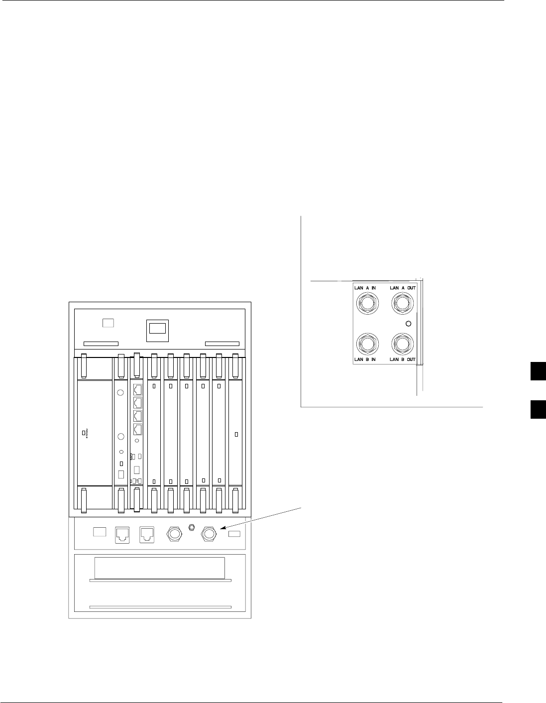
Ethernet LAN Termination
For proper operation, the BTS Ethernet Local Area Network (LAN)
connections must be terminated with a 50–ohm loads. This is done by
placing four (4) 50–ohm BNC terminations on the LAN A and B
external IN and OUT connectors located on the rear of the BTS. This is
only done on stand–alone BTSs. The front panel LAN connections are
not terminated with loads.
Verify that the LAN A and B external IN and OUT connectors at the rear
of the BTS have terminations installed. See Figure 6-1 for locations.
Figure 6-1: LAN Connectors
19MHz EVEN RESET ALARM MMI
PWR/ALM
PWR/ALM
PWR/ALM
PWR/ALM
PWR/ALM
PWR/ALM
RESET
GLI
ACTIVE
ACTIVE
ACTIVE
ACTIVE
ACTIVE
BPR A BPR B AUX
MMI
MMI
LAN A & B
Connections
P/O Rear Panel
Rear Panel LAN Connectors
LAN A LAN B
Front Panel
6

Introduction to Optimization and Calibration
6-4 1X SC480 BTS Hardware Installation, Optimization/ATP, and FRU Jun 2004
DRAFT
Overview
This section describes procedures for isolating the BTS from the span
lines, preparing and using the WinLMF, downloading system operating
software, CSA reference verification/optimization, set up and calibration
of the supported test equipment, and transmit/receive paths are
functioning properly.
Before using the WinLMF, use an editor to view the
“CAVEATS” section in the “readme.txt” file in the c:\wlmf
folder for any applicable information.
NOTE
Optimization Process
Summary
After a BTS is physically installed and the preliminary operations, such
as power up, have been completed, the WinLMF is used to optimize the
BTS. The basic optimization process consists of the following:
1. Download GLI3 (GLI–bts#–1) with application code and data and
then enable GLI3.
2. Use the WinLMF status function and verify that all of the installed
devices of the following types respond with status information:
CSA, BBX, GLI3, and MCC. If a device is installed and powered up
but is not responding and is colored gray in the BTS display, the
device is not listed in the CDF file. The CDF/NECF file must be
corrected before the device can be accessed by the WinLMF.
3. Download device application code and data to all devices of the
following types:
– CSA
– BBX–1X
– MCC–1X
4. Verify the operation of the GPS and HSO/MSO signals.
5. Using the WinLMF test equipment selection function, select the test
equipment to be used for the calibration.
6. Calibrate the TX and RX test cables if they have not previously been
calibrated with the WinLMF computer and software build which will
be used for the optimization/calibration. Cable calibration values can
be entered manually, if required.
7. Connect the required test equipment for a full optimization.
8. Select all of the BBXs and all of the MCCs and use the full
optimization function. The full optimization function performs TX
calibration, BLO download, TX audit, all TX tests, and all RX tests
for all selected devices.
9. If the TX calibration fails, repeat the full optimization for any failed
paths.
6

Introduction to Optimization and Calibration – continued
Jun 2004 1X SC480 BTS Hardware Installation, Optimization/ATP, and FRU 6-5
DRAFT
10. If the TX calibration fails again, troubleshoot and correct the
problem causing the failure, and repeat the full optimization for the
failed path.
11. If the TX calibration and audit portion of the full optimization passes
for a path but some of the TX or RX tests fail, troubleshoot and
correct the problem causing the failure, and run the individual tests
as required until all TX and RX tests have passed for all paths.
Cell-site Types
The site is configured as Omni/Omni. Each cell site type has unique
characteristics and must be optimized accordingly.
CDF/NECF
The CDF/NECF (Configuration Data File/Network Element
Configuration File) contains information that defines the BTS and data
used to download files to the devices. A CDF/NECF file must be placed
in the applicable BTS folder before the WinLMF can be used to log into
that BTS. CDF/NECF files are normally obtained from the CBSC using
a floppy disk. A file transfer protocol (ftp) method can be used if the
WinLMF computer has that capability. Refer to the WinLMF Help
function on–line documentation for more information.
The CDF/NECF includes the following information:
SDownload instructions and protocol
SSite specific equipage information
SCCP2 Shelf allocation plan
– BBX equipage (based on cell–site type) including IS–95A/B or
CDMA2000 1X capability and redundancy
– CSA equipage including redundancy
– Multi–Channel CDMA Card 1X channel element allocation plan.
This plan indicates how the CCP2 Shelf is configured, and how the
paging, synchronization, traffic, and access channel elements (and
associated gain values) are assigned among the (up to 3) MCC–1Xs
in the shelf.
SEffective Rated Power (ERP) table for all TX channels to antennas
respectively. Motorola System Engineering specifies the ERP of a
transmit antenna based on site geography, antenna placement, and
government regulations. Working from this ERP requirement, antenna
gain and antenna feed line loss can be combined to calculate the
required transmit power at the frame antenna connections. The
corresponding BBX output power required to achieve that power level
on any channel/sector can then be determined based on Bay Level
Offset (BLO) data established during the optimization process.
6

Introduction to Optimization and Calibration – continued
6-6 1X SC480 BTS Hardware Installation, Optimization/ATP, and FRU Jun 2004
DRAFT
Refer to Figure 6-2 and the WinLMF Help function on–line
documentation for additional information on the layout of
the WinLMF directory structure (including CDF/NECF file
locations and formats).
NOTE
BTS System Software
Download
BTS system software must be successfully downloaded to the BTS
processor boards before optimization can be performed. BTS operating
code is loaded from the WinLMF computer terminal.
The BTS is configured for Circuit Backhaul and uses bts.cdf files. BTSs
configured for Packet Backhaul use bts.necf files (bts–xxx.xml) located
on the OMC–R.
Before using the WinLMF for optimization/ATP, the
correct bts–#.cdf (or bts–#.necf) and cbsc–#.cdf files for
the BTS must be obtained from the CBSC and put in a
bts–# folder in the WinLMF. Failure to use the correct
CDF/NECF files can cause wrong results. Failure to use
the correct CDF/NECF files to log into a live (traffic
carrying) site can shut down the site.
NOTE
The CDF/NECF is normally obtained from the CBSC on a DOS
formatted diskette, or through a file transfer protocol (ftp) if the
WinLMF computer has ftp capability. Refer to the WinLMF Help
function on–line documentation for the procedure.
Site Equipage Verification
If you have not already done so, use an editor to view the CDF/NECF,
and review the site documentation. Verify the site engineering equipage
data in the CDF/NECF matches the actual site hardware using a
CDF/NECF conversion table.
Use extreme care not to make any changes to the
CDF/NECF content while viewing the file. Changes to the
CDF/NECF can cause the site to operate unreliably or
render it incapable of operation.
Always wear a conductive, high impedance wrist strap
while handling any circuit card/module to prevent damage
by ESD. Extreme care should be taken during the removal
and installation of any card/module. After removal, the
card/module should be placed on a conductive surface or
back into the anti–static bag in which it was shipped.
CAUTION
6

Preparing the LMF
Jun 2004 1X SC480 BTS Hardware Installation, Optimization/ATP, and FRU 6-7
DRAFT
Overview of Packet BTS files
R16.0 and earlier releases had the configuration file called CDF for each
BTS and CBSC used by WinLMF. In 16.1 Packet BTS, BTS with GLI3
booting in packet binary, the CDF is replaced by two new configuration
files called Network Element Configuration Base (NECB) and Network
Element Change Journal (NECJ). The NECB contains the baseline
configuration and is analogous to the CDF, while the NECJ contains all
the changes made to the configuration since the last time the NECB was
re–generated. Once the NECJ gets to 80% of its maximum size, the
NECB is re–generated and all the updates are rolled into it.
These files play much broader and vital role than previous CDF files.
GLI3 booting in circuit binaries works similar to R16.0.
A few WinLMF related important facts about these files are listed below.
SBoth files (NECB and NECJ) are in XML format.
SNECB contains all the up-to-date static configuration information and
NECJ contains all the recent changes (including operations) which are
not updated in the NECB.
SBoth files can be viewed in any XML viewer (most easily available is
Internet Explorer V5.0 and higher). They can be also viewed by any
other word processor, but the XML tags will also be seen with them.
SThese files will be created by OMC–R from MIB as per the BTS
provisioning.
SThese files will be regenerated for each software release upgrade on
the system for each BTS.
SThese files will reside on both OMC–R and Packet–GLI3 (unlike
CDF) and will be synchronized periodically between them.
SBoth NECB and NECJ file contain a “SoftwareVersion” field in their
header section indicating the system release version of these files.
SInstead of the bts#.cdf file, the packet WinLMF uses a bts#.XML file,
which is a copy of the NECB.XML file.
SPacket–GLI3 will need these files for site initialization.
SThe scope of NECB has grown much broader than CDF and has much
more BTS centric information. The use of generic version of these
files should be strictly avoided for the correct site initialization.
6

Preparing the LMF – continued
6-8 1X SC480 BTS Hardware Installation, Optimization/ATP, and FRU Jun 2004
DRAFT
WinLMF Features and
Installation Requirements
Before optimization can be performed, the WinLMF application software
must be installed and configured on a computer platform meeting
Motorola–specified requirements.
For the WinLMF graphics to display properly, the
computer platform must be configured to display more
than 256 colors. See the operating system software
instructions for verifying and configuring the display
settings.
NOTE
Software and files for installing and updating the WinLMF are provided
on CD ROM disks. The following items must be available:
SWinLMF application program on CD ROM
SCDF/NECF for each supported BTS (on diskette or available from the
CBSC)
SCBSC File for each supported BTS (on floppy disk or CD ROM)
FTP Server
To be able to download files to the GLI3, the WinLMF now runs FTP
server on the WinLMF laptop. The WinLMF FTP server runs from the
LMFs home directory. All the files necessary to run the WinLMF FTP
server are installed from the WinLMF CD. The FTP server is
automatically started by the WinLMF upon successful Login to a Packet
BTS.
In addition, the WinLMF provides a new option in the Tools menu called
FTP Server. The option starts the LMFs FTP server if Start is selected,
and stops the server if Stop is selected. The LMFs FTP server runs on
port 21. If any other process is using that port, the error message is
displayed to the user stating that the port is occupied. There is another
option under FTP Server menu called FTP Monitor, which allows the
user to watch FTP activity b/w the WinLMF and GLI.
Firewalls
Firewalls will block the FTP requests from the Packet GLI to the
WinLMF laptop. You must disable your firewall before attempting the
BTS Synch command. Some common firewall programs to look for
include Network ICE, BlackICE, Norton’s Desktop Firewall, Enterprise
Firewall, and Personal Firewall.
6

Preparing the LMF – continued
Jun 2004 1X SC480 BTS Hardware Installation, Optimization/ATP, and FRU 6-9
DRAFT
FTP Server Port in use
On some Windows 2000 installations, a process called “inetd.exe”
makes the FTP server port 21 unusable by the WinLMF. If the WinLMF
reports that the FTP server could not start because the port is in use,
make sure the inetd.exe is not running by using the Task Manager’s
process list. If inetd.exe is running, end the process by selecting it and
clicking the “End Process” button. Inetd32.exe is NOT the same and
ending it will not resolve this problem.
WinLMF File Structure
Overview
The WinLMF uses a <x>:\<lmf home directory> folder that contains all
of the essential data for installing and maintaining the BTS. The
following list outlines the folder structure for WinLMF. Except for the
bts-nnn folders, these folders are created as part of the WinLMF
installation. Refer to the CDMA WinLMF Operator’s Guide for a
complete description of the folder structure.
Figure 6-2: WinLMF Folder Structure
version folder (A separate folder is
required for each different version; for
example, a folder name 2.8.1.1.1.5.)
loads folder
(C:)
x:\<lmf home directory> folder
cdma folder
code folder
data folder
BTS–nnn folders (A separate folder is
required for each BTS where bts–nnn is the
unique BTS number; for example, bts–163.)
The “loads” folder and all the folders below it are not
available from the WinLMF for Software Release 2.16.3.x.
These folders may be present as as a legacy from previous
software versions or downloaded from the OMC–R/CBSC.
NOTE
WinLMF Home Directory
The WinLMF installation program creates the default home directory,
c:\wlmf, and installs the application files and subdirectories (folders)
in it. Because this can be changed at installation, the CDMA WinLMF
home directory will be referred to with the generic convention of:
6

Preparing the LMF – continued
6-10 1X SC480 BTS Hardware Installation, Optimization/ATP, and FRU Jun 2004
DRAFT
<x>:\<lmf home directory>
Where:
<x> = the WinLMF computer drive letter where the CDMA WinLMF
home directory is located.
<lmf home directory> = the directory path or name where the CDMA
WinLMF is installed.
NECF Filename Conventions
and Directory Location
NECF
The NECF actually consists of two files: the NECB and NECJ. The
naming convention for the NECB and NECJ is:
NECB*bts#.xml
NECJ*bts#.xml
Where:
* = any characters can be substituted there
# = the actual integer BTS number
The NECB and its corresponding NECJ must have the exact same name,
except for the “B” and “J” difference after the initial NEC characters.
The NECB and the NECJ must reside in the
<WinLMF_HOME>\cdma\bts–# directory corresponding to the BTS
frame they are for.
Load Information File (LIF)
The LIF contains all the devices binaries available for the specified
System Software Release. It is the functional equivalent of the OLF file
that was used pre–Packet.
The naming convention for the LIF is:
NE_LIF.xml
The LIF must reside in the <WinLMF_HOME>\cdma\loads\<Software
Release Number> directory, where <WinLMF_HOME> = the home
directory in which the WinLMF is installed, usually C:\wlmf <Software
Release Number> = the System Software Release Number (e.g.
2.16.1.0.10).
Cal File
The Cal File still resides in the <WinLMF_HOME>\cdma\bts–#
directory and is named bts–#.cal, where # is the actual integer number of
the BTS.
6

Preparing the LMF – continued
Jun 2004 1X SC480 BTS Hardware Installation, Optimization/ATP, and FRU 6-11
DRAFT
WinLMF Operating System
Installation
This section provides information and instructions for installing and
updating the WinLMF software and files.
First Time Installation Sequence
SInstall Java Runtime Environment (JRE)
SInstall U/WIN K–shell emulator
SInstall WinLMF application programs
SInstall/create BTS folders
Any time you install U/WIN, you must install the
WinLMF software because the installation of the WinLMF
modifies some of the files that are installed during the
U/Win installation. Installing U/Win over–writes these
modifications.
There are multiple binary image packages for installation
on the CD–ROM. When prompted, choose the load that
corresponds to the switch release that you currently have
installed. Perform the Device Images install after the
WinLMF installation.
If applicable, a separate CD ROM of BTS Binaries may be
available for binary updates.
NOTE
Follow the procedure in Table 6-2 to install the WinLMF application
program using the WinLMF CD ROM.
Table 6-2: Install WinLMF using CD ROM
nStep Action
1Insert the WinLMF CD ROM disk into your disk drive and perform the following as required:
1a – If the Setup screen appears, follow the instructions displayed on the screen.
1b – If the Setup screen is not displayed, proceed to Step 2.
2Click on the Start button
3 Select Run.
4 Enter d:\autorun in the Open box and click OK.
NOTE
If applicable, replace the letter d with the correct CD ROM drive letter.
6

Preparing the LMF – continued
6-12 1X SC480 BTS Hardware Installation, Optimization/ATP, and FRU Jun 2004
DRAFT
Copy BTS CDF (or NECF) and
CBSC CDF Files to the WinLMF
Computer
Before logging on to a BTS with the WinLMF computer to execute
optimization/ATP procedures, the correct bts-#.cdf (or bts–#.necf) and
cbsc-#.cdf files must be obtained from the CBSC and put in a bts-#
folder in the WinLMF computer. This requires creating versions of the
CBSC CDF files on a DOS–formatted floppy diskette and using the
diskette to install the CDF files on the WinLMF computer.
If the WinLMF has ftp capability, the ftp method can be
used to copy the CDF or NECF files from the CBSC.
On Sun OS workstations, the unix2dos command can be
used in place of the cp command (e.g., unix2dos
bts–248.cdf bts–248.cdf). This should be done using a
copy of the CBSC CDF file so the original CBSC CDF file
is not changed to DOS format.
When copying CDF or NECF files, comply with the
following to prevent BTS login problems with the
Windows WinLMF:
– The numbers used in the bts-#.cdf (or bts–#.necf)
and cbsc-#.cdf filenames must correspond to the
locally-assigned numbers for each BTS and its
controlling CBSC.
– The generic cbsc–1.cdf file supplied with the
Windows WinLMF will work with locally numbered
BTS CDF files. Using this file will not provide a
valid optimization unless the generic file is edited to
replace default parameters (e.g., channel numbers)
with the operational parameters used locally.
NOTE
The procedure in Table 6-3 lists the steps required to transfer the CDF
files from the CBSC to the WinLMF computer. For further information,
refer to the WinLMF Help function on–line documentation.
Table 6-3: Copying CDF or NECF Files to the WinLMF Computer
nStep Action
AT THE CBSC:
1Login to the CBSC workstation.
2Insert a DOS–formatted floppy diskette in the workstation drive.
3 Type eject –q and press the Enter key.
. . . continued on next page
6

Preparing the LMF – continued
Jun 2004 1X SC480 BTS Hardware Installation, Optimization/ATP, and FRU 6-13
DRAFT
Table 6-3: Copying CDF or NECF Files to the WinLMF Computer
nActionStep
4 Type mount and press the Enter key.
NOTE
SLook for the “floppy/no_name” message on the last line displayed.
SIf the eject command was previously entered, floppy/no_name will be appended with a number.
Use the explicit floppy/no_name reference displayed when performing step 7.
5Change to the directory, where the files to be copied reside, by typing cd <directoryname>
(e.g., cd bts–248) and pressing the Enter key.
6 Type ls and press the Enter key to display the list of files in the directory.
7 With Solaris versions of Unix, create DOS–formatted versions of the bts-#.cdf (or bts–#.necf) and
cbsc-#.cdf files on the diskette by entering the following command:
unix2dos <source filename> /floppy/no_name/<target filename>
(e.g., unix2dos bts–248.cdf /floppy/no_name/bts–248.cdf).
NOTE
SOther versions of Unix do not support the unix2dos and dos2unix commands. In these cases, use
the Unix cp (copy) command. The copied files will be difficult to read with a DOS or Windows text
editor because Unix files do not contain line feed characters. Editing copied CDF files on the
WinLMF computer is, therefore, not recommended.
SUsing cp, multiple files can be copied in one operation by separating each filename to be copied
with a space and ensuring the destination directory (floppy/no_name) is listed at the end of the
command string following a space (e.g., cp bts–248.cdf cbsc–6.cdf /floppy/no_name).
8Repeat Steps 5 through 7 for each bts–# that must be supported by the WinLMF computer.
9When all required files have been copied to the diskette type eject and press the Enter key.
10 Remove the diskette from the CBSC drive.
AT THE WinLMF:
11 If it is not running, start the Windows operating system on the WinLMF computer.
12 Insert the diskette containing the bts-#.cdf (or bts–#.necf) and cbsc-#.cdf files into the WinLMF
computer.
13 Using MS Windows Explorer, create a corresponding bts–# folder in the <x>:\<lmf home
directory>\cdma directory for each bts–#.cdf/cbsc–#.cdf (or bts–#.necf/cbsc–#.cdf) file pair copied
from the CBSC.
14 Use MS Windows Explorer to transfer the bts-#.cdf (or bts–#.necf) and cbsc-#.cdf files from the
diskette to the corresponding <x>:\<lmf home directory>\cdma\bts–# folders created in Step 13.
6

Preparing the LMF – continued
6-14 1X SC480 BTS Hardware Installation, Optimization/ATP, and FRU Jun 2004
DRAFT
Creating a Named
HyperTerminal Connection for
MMI Communication
Confirming or changing the configuration data of certain BTS Field
Replaceable Units (FRU) requires establishing an MMI communication
session between the WinLMF and the FRU. Using features of the
Windows operating system, the connection properties for an MMI
session can be saved on the WinLMF computer as a named Windows
HyperTerminal connection. This eliminates the need for setting up
connection parameters each time an MMI session is required to support
optimization.
Once the named connection is saved, a shortcut for it can be created on
the Windows desktop. Double–clicking the shortcut icon will start the
connection without the need to negotiate multiple menu levels.
Follow the procedures in Table 6-4 to establish a named HyperTerminal
connection and create a Windows desktop shortcut for it.
Table 6-4: Create HyperTerminal Connection
Step Action
1From the Windows Start menu, select:
Programs>Accessories>
2Perform one of the following:
SFor Win NT, select Hyperterminal and then click on HyperTerminal or
SFor Win 98, select Communications, double click the Hyperterminal folder, and then double click
on the Hyperterm.exe icon in the window that opens.
NOTE
SIf a Location Information Window appears, enter the required information, then click on the
Close button. (This is required the first time, even if a modem is not to be used.)
SIf a You need to install a modem..... message appears, click on NO.
3When the Connection Description box opens:
– Type a name for the connection being defined (e.g., MMI Session) in the Name: window,
– Highlight any icon preferred for the named connection in the Icon: chooser window, and
– Click OK.
4From the Connect using: pick list in the Connect To box displayed, select COM1 or COM2 (Win
NT) – or Direct to Com 1 or Direct to Com 2 (Win 98) for the RS–232 port connection and click OK.
NOTE
For WinLMF computer configurations where COM1 is used by another interface such as test
equipment and a physical port is available for COM2, select COM2 in the following step to prevent
conflicts.
. . . continued on next page
6

Preparing the LMF – continued
Jun 2004 1X SC480 BTS Hardware Installation, Optimization/ATP, and FRU 6-15
DRAFT
Table 6-4: Create HyperTerminal Connection
Step Action
5In the Port Settings tab of the COM# Properties window displayed, configure the RS–232 port
settings as follows:
SBits per second: 9600
SData bits: 8
SParity: None
SStop bits: 1
SFlow control: None
6 Click OK.
7Save the defined connection by selecting:
File > Save
8Close the HyperTerminal window by selecting:
File > Exit
9Click the Yes button to disconnect when prompted.
10 Perform one of the following:
SIf the Hyperterminal folder window is still open (Win 98) proceed to step 12
SFrom the Windows Start menu, select Programs > Accessories.
11 Perform one of the following:
SFor Win NT, select Hyperterminal and release any pressed mouse buttons.
SFor Win 98, select Communications and double click the Hyperterminal folder.
SFor Win–XP, select Communications and double click the Hyperterminal folder.
12 Highlight the newly–created connection icon by clicking on it.
13 Right click and drag the highlighted connection icon to the Windows desktop and release the right
mouse button.
14 From the popup menu which appears, select Create Shortcut(s) Here.
15 If desired, reposition the shortcut icon for the new connection by dragging it to another location on the
Windows desktop.
16 Close the Hyperterminal folder window by selecting:
File > Close
6
Span Lines – Interface and Isolation
JUN 2004
1X SC480 BTS Hardware Installation, Optimization/ATP, and FRU
DRAFT
6-16
T1/E1 Span Interface
At active sites, the OMC–R/CBSC must disable the BTS
and place it out–of–service (OOS). DO NOT remove the
span line cable connectors until the OMC–R/CBSC has
disabled the BTS.
NOTE
Before connecting the WinLMF computer to the BTS LAN, the
OMC–R/CBSC must disable the BTS and place it OOS. This will allow
the WinLMF to control the BTS, and prevent the CBSC from
inadvertently sending control information to the BTS during
WinLMF–based tests.
Isolate BTS from T1/E1 Spans
Once the OMC–R/CBSC has disabled the BTS, the spans must be
disabled to ensure the WinLMF will maintain control of the BTS.
T1/E1 Span Isolation
Table 6-5 describes the action required for span isolation.
Table 6-5: T1/E1 Span Isolation
Step Action
1Have the OMC–R/CBSC operator place the BTS OOS.
2To disable the span lines, disconnect the span or spans from the CBIO Network Span–1X or Group 1
Span–EVDO sockets.
If in an outdoor configuration, then unlock and open TME left side door to gain access to rear of BTS.
6
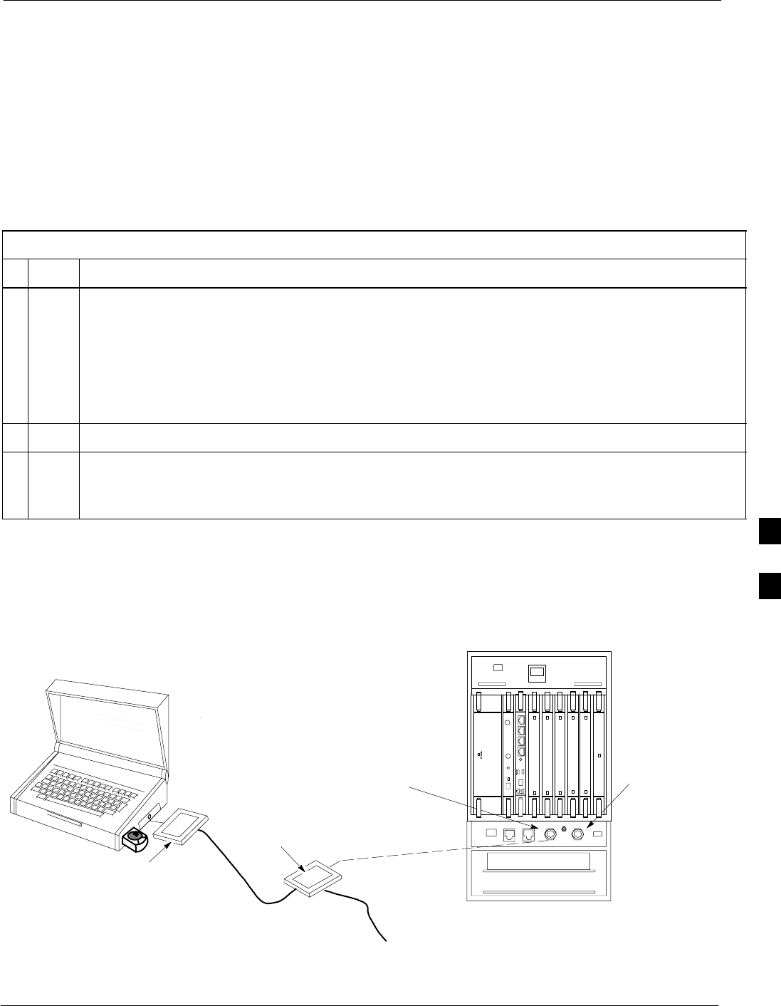
LMF to BTS Connection
JUN 2004 1X SC480 BTS Hardware Installation, Optimization/ATP, and FRU
DRAFT
6-17
Connect the WinLMF to the
BTS
The WinLMF computer may be connected to the LAN A or B connector
located on the front panel or at the rear of the BTS. Figure 6-3 below
shows the general location of these connectors. LAN A is considered the
primary LAN.
Table 6-6: Connecting the WinLMF to the BTS
nStep Action
1For indoor configuration, remove BTS front panel cover.
For outdoor configuration, unlock and open TME right side door and remove BTS front panel cover.
NOTE
Xircom Model PE3–10B2 or equivalent can also be used to interface the WinLMF Ethernet
connection to the BTS frame connected to the PC parallel port, powered by an external AC/DC
transformer. In this case, the BNC cable must not exceed 91 cm (3 ft) in length.
2Connect the WinLMF computer to the LAN A (left–hand) BNC connector . (See Figure 6-3)
* IMPORTANT
The LAN shield is isolated from chassis ground. The LAN shield (exposed portion of BNC connector)
must not touch the chassis during optimization.
ETHERNET B LMF
CONNECTION
Remove panel to gain
access to the site 1 or
site 2 LMF BNC
connector. ETHERNET A LMF
CONNECTION
PCMCIA ETHERNET
ADAPTER
10BASET/10BASE2
CONVERTER CONNECTS
DIRECTLY TO LAN A
115 VAC POWER
CONNECTION
FRONT OF BTS
WITH PANEL
COVER REMOVED
Figure 6-3: WinLMF Connection Detail
If lap top is equipped with an
ethernet port, then PCMCIA
ethernet adapter is not required
6

Using the LMF
6-18 1X SC480 BTS Hardware Installation, Optimization/ATP, and FRU Jun 2004
DRAFT
Basic LMF Operation
LMF Coverage in This Publication – The LMF application program
supports maintenance of both CDMA and SAS BTSs. All references to
the LMF in this publication are to the CDMA portion of the program.
Operating Environments – The LMF application program allows the
user to work in the two following operating environments which are
accessed using the specified desktop icons:
SGraphical User Interface (GUI) using the WinLMF icon
SCommand Line Interface (CLI) using the WinLMF CDMA CLI icon
The GUI is the primary optimization and acceptance testing operating
environment. The CLI environment provides additional capability to the
user to perform manually controlled acceptance tests and audit the
results of optimization and calibration actions.
Basic Operation – Basic operation of the LMF in either environment
includes performing the following:
SSelecting and deselecting BTS devices
SEnabling devices
SDisabling devices
SResetting devices
SObtaining device status
The following additional basic operation can be performed in a GUI
environment:
SSorting a status report window
For detailed information on performing these and other LMF operations,
refer to the LMF Help function on–line documentation.
Unless otherwise noted, LMF procedures in this manual
are performed using the GUI environment.
NOTE
6

Using the LMF – continued
Jun 2004 1X SC480 BTS Hardware Installation, Optimization/ATP, and FRU 6-19
DRAFT
The LMF Display and the BTS
BTS Display – When the LMF is logged into a BTS, a frame tab is
displayed for each BTS frames. The frame tab will be labeled with
“CDMA” and the BTS number, a dash, and the frame number (for
example, BTS–812–1 for BTS 812, RFMF 1). If there is only one frame
for the BTS, there will only be one tab.
CDF/NECF Requirements – For the LMF to recognize the devices
installed in the BTS, a BTS CDF/NECF file which includes equipage
information for all the devices in the BTS must be located in the
applicable <x>:\<lmf home directory>\cdma\bts–# folder. To provide
the necessary channel assignment data for BTS operation, a CBSC CDF
file which includes channel data for all BTS RFMFs is also required in
the folder.
Graphical User Interface
Overview
The LMF uses a GUI, which works in the following way:
SSelect the device or devices.
SSelect the action to apply to the selected device(s).
SWhile action is in progress, a status report window displays the action
taking place and other status information.
SThe status report window indicates when the the action is complete
and displays other pertinent information.
SClicking the OK button closes the status report window.
Understanding GUI Operation
The following screen captures are provided to help understand how the
GUI operates:
– Figure 6-4 depicts the differences between packet and circuit
CDMA “cdf” file identification. Note that if there is a packet
version “bts” file, the “(P)” is added as a suffix. There is a
corresponding “(C)” for the circuit mode version.
– Figure 6-5 depicts the Self-Managed Network Elements (NEs) state
of a packet mode. Note that an “X” is on the front of each card that
is under Self–Managed Network Elements (NEs) control by the
GLI3 card.
– Figure 6-6 depicts three of the available packet mode commands.
Normally the GLI3 has Self-Managed Network Elements (NEs)
control of all cards as shown in Figure 6-5 by an “(X)”. In that state
the LMF may only status a card. In order to download code or test a
card, the LMF must request Self-Managed Network Elements (NEs)
control of the card by using the shown dropdown menu. It also uses
this menu to release control of the card back to the GLI3. The GLI3
will also assume control of the cards after the LMF logs out of the
BTS. The packet mode GLI3 normally is loaded with a tape release
6
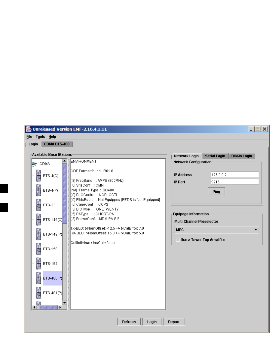
Using the LMF – continued
6-20 1X SC480 BTS Hardware Installation, Optimization/ATP, and FRU Jun 2004
DRAFT
and NECB and NECJ files which point to a tape release stored on
the GLI3. When the GLI3 has control of a card it will maintain that
card with the code on that tape release.
– Figure 6-7 depicts a packet mode site that has the MCC–1 and the
BBX–1 cards under LMF control. Notice that the “X” is missing
from the front of these two cards.
For detailed information on performing these and other LMF operations,
refer to the LMF Help function on–line documentation.
Figure 6-4: BTS Login Screen – Identifying Circuit and Packet BTS Files
6
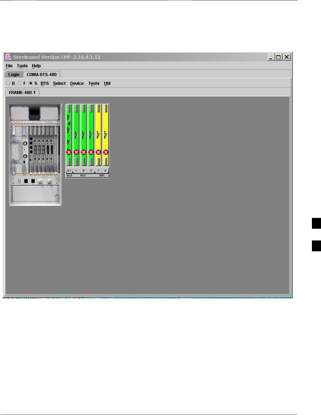
Using the LMF – continued
Jun 2004 1X SC480 BTS Hardware Installation, Optimization/ATP, and FRU 6-21
DRAFT
Figure 6-5: Self–Managed Network Elements (NEs) State of a Packet Mode
6
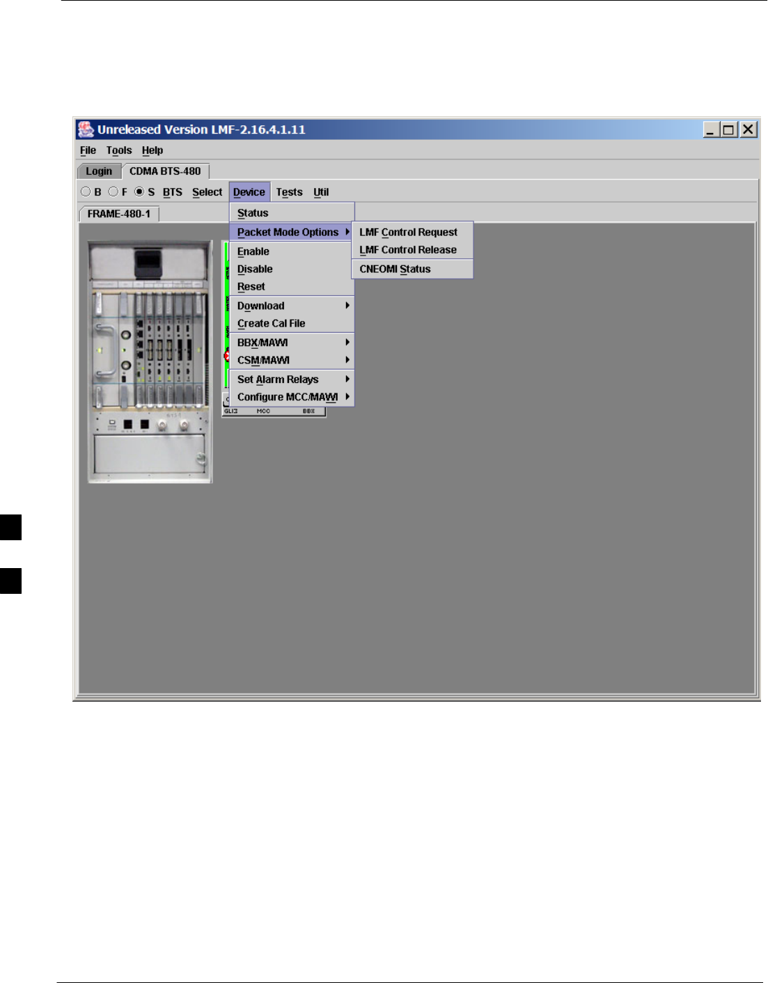
Using the LMF – continued
6-22 1X SC480 BTS Hardware Installation, Optimization/ATP, and FRU Jun 2004
DRAFT
Figure 6-6: Available Packet Mode Commands
6
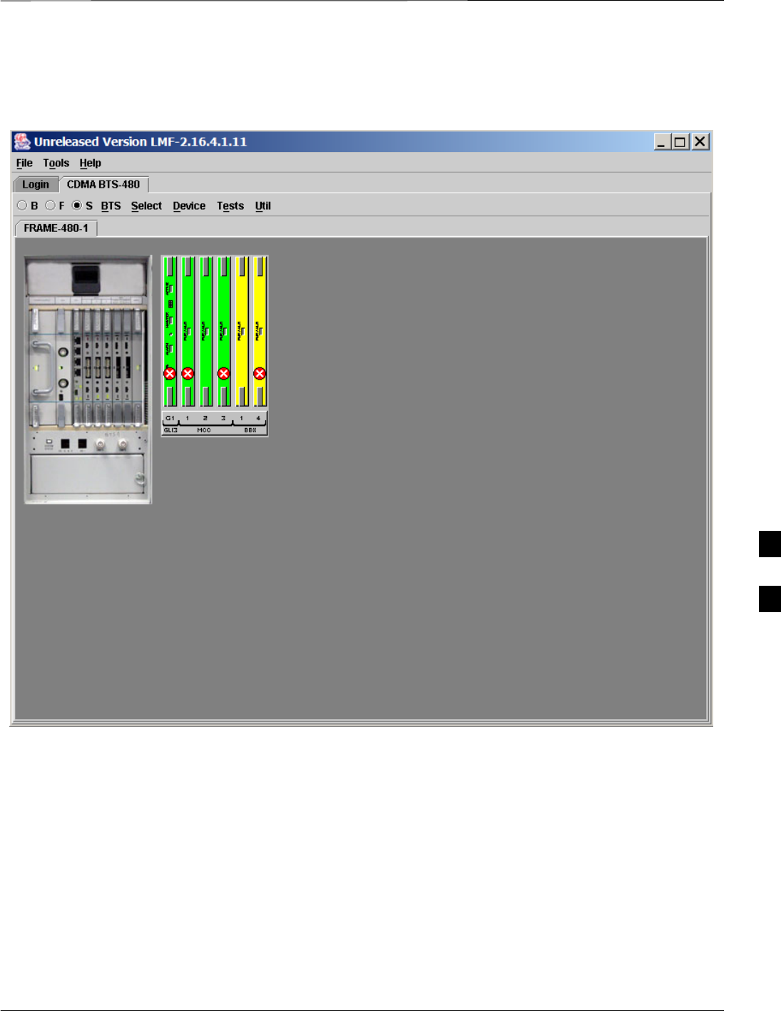
Using the LMF – continued
Jun 2004 1X SC480 BTS Hardware Installation, Optimization/ATP, and FRU 6-23
DRAFT
Figure 6-7: Packet Mode Site with MCC–1 and BBX–1 under LMF Control
6

Using the LMF – continued
6-24 1X SC480 BTS Hardware Installation, Optimization/ATP, and FRU Jun 2004
DRAFT
Command Line Interface
Overview
The LMF also provides Command Line Interface (CLI) capability.
Activate the CLI by clicking on a shortcut icon on the desktop. The CLI
can not be launched from the GUI, only from the desktop icon.
Both the GUI and the CLI use a program known as the handler. Only one
handler can be running at one time. The architectural design is such that
the GUI must be started before the CLI if you want the GUI and CLI to
use the same handler.
When the CLI is launched after the GUI, the CLI automatically finds and
uses an in–progress login session with a BTS initiated under the GUI.
This allows the use of the GUI and the CLI in the same BTS login
session.
If a CLI handler is already running when the GUI is launched (this
happens if the CLI window is already running when the user starts the
GUI, or if another copy of the GUI is already running when the user
starts the GUI), a dialog window displays the following warning
message:
The CLI handler is already running.
This may cause conflicts with the LMF.
Are you sure that you want to start the application?
This window also contains yes and no buttons. Selecting yes starts the
application. Selecting no terminates the application.
CLI Format Conventions
The CLI command can be broken down in the following way:
SVerb
SDevice including device identifier parameters
SSwitch
SOption parameters consisting of:
– Keywords
– Equals sign (=) between the keyword and the parameter value
– Parameter values
Spaces are required between the verb, device, switch, and option
parameters. A hyphen is required between the device and its identifiers.
Following is an example of a CLI command.
measure bbx–<bts_id>–<bbx_id> rssi channel=6 sector=5
Refer to the LMF CLI Commands for a complete explanation of the CLI
commands and their usage.
6
Using the LMF – continued
Jun 2004 1X SC480 BTS Hardware Installation, Optimization/ATP, and FRU 6-25
DRAFT
Logging Into a BTS
Logging into a BTS establishes a communication link between the BTS
and the LMF. An LMF session can be logged into only one BTS at a
time.
Prerequisites
Before attempting to log into a BTS, ensure the following have been
completed:
SThe LMF is correctly installed on the LMF computer.
SA bts-nnn folder with the correct CDF/NECF and CBSC files exists.
SThe LMF computer was connected to the BTS before starting the
Windows operating system and the LMF software. If necessary, restart
the computer after connecting it to the BTS in accordance with
Table 6-6 and Figure 6-3.
Be sure that the correct bts–#.cdf/necf and cbsc–#.cdf file
are used for the BTS. These should be the CDF/NECF files
that are provided for the BTS by the CBSC. Failure to use
the correct CDF/NECF files can result in invalid
optimization. Failure to use the correct CDF/NECF files
to log into a live (traffic–carrying) site can shut down
the site.
CAUTION
BTS Login from the GUI Environment
Follow the procedures in Table 6-7 to log into a BTS when using the
GUI environment.
Table 6-7: BTS GUI Login Procedure
nStep Action
1Start the LMF GUI environment by double–clicking on the WinLMF desktop icon (if the LMF is
not running).
– An LMF window will open and display the LMF build number in the title bar.
NOTE
If a warning similar to the following is displayed, select No, shut down other LMF sessions which
may be running, and start the LMF GUI environment again:
The CLI handler is already running.
This may cause conflicts with the LMF.
Are you sure you want to start the application?
Yes No
2Click on Login tab (if not displayed).
3Double click on CDMA (in the Available Base Stations pick list).
. . . continued on next page
6

Using the LMF – continued
6-26 1X SC480 BTS Hardware Installation, Optimization/ATP, and FRU Jun 2004
DRAFT
Table 6-7: BTS GUI Login Procedure
nActionStep
4Click on the desired BTS number.
5Click on the Network Login tab (if not already in the forefront).
6Enter correct IP address (normally 128.0.0.2) for a field BTS, if not correctly displayed in the IP
Address box.
7Type in the correct IP Port number (normally 9216) if not correctly displayed in the IP Port box.
8Click on Ping.
– If the connection is successful, the Ping Display window shows text similar to the following:
Reply from 128 128.0.0.2: bytes=32 time=3ms TTL=255
– If there is no response the following is displayed:
128.0.0.2:9216:Timed out
If the GLI fails to respond, reset and perform the ping process again. If the GLI still fails to
respond, typical problems are shorted BNC to inter–frame cabling, open cables, crossed A and B
link cables, missing 50–Ohm terminators, or the GLI itself.
9If required, match the device corresponding to the BTS configuration by selecting
Multi-channel Preselector type from the Multi-channel Preselector drop–down list (default is
MPC).
10 Click on Login. (A BTS tab with the BTS and frame numbers is displayed.)
NOTE
SIf an attempt is made to log into a BTS that is already logged on, all devices will be gray.
SThere may be instances where the BTS initiates a log out due to a system error (i.e., a device
failure).
SIf the GLI is OOS–ROM (blue), it must be downloaded with RAM code before other devices
can be seen.
SIf the GLI is OOS–RAM (yellow), it must be enabled before other installed devices can be seen.
6

Using the LMF – continued
Jun 2004 1X SC480 BTS Hardware Installation, Optimization/ATP, and FRU 6-27
DRAFT
BTS Login from the CLI Environment
Follow the procedures in Table 6-8 to log into a BTS when using the
CLI environment.
If the CLI and GUI environments are to be used at the
same time, the GUI must be started first and BTS login
must be performed from the GUI. Refer to Table 6-7 to
start the GUI environment and log into a BTS.
NOTE
Table 6-8: BTS CLI Login Procedure
nStep Action
1Double–click the WinLMF CLI desktop icon (if the LMF CLI environment is not already
running).
NOTE
If a BTS was logged into under a GUI session before the CLI environment was started, the CLI
session will be logged into the same BTS, and step 2 is not required.
2At the /wlmf prompt, enter the following command:
login bts–<bts#> host=<host> port=<port>
where:
host = GLI card IP address (defaults to address last logged into for this BTS or 128.0.0.2 if this is
first login to this BTS)
port = IP port of the BTS (defaults to port last logged into for this BTS or 9216 if this is first login
to this BTS)
A response similar to the following will be displayed:
LMF>
13:08:18.882 Command Received and Accepted
COMMAND=login bts–33
13:08:18.882 Command In Progress
13:08:21.275 Command Successfully Completed
REASON_CODE=”No Reason”
6

Using the LMF – continued
6-28 1X SC480 BTS Hardware Installation, Optimization/ATP, and FRU Jun 2004
DRAFT
Logging Out
Logging out of a BTS is accomplished differently for the GUI and CLI
operating environments.
The GUI and CLI environments use the same connection to
a BTS. If a GUI and the CLI session are running for the
same BTS at the same time, logging out of the BTS in
either environment will log out of it for both. When either
a login or logout is performed in the CLI window, there is
no GUI indication that the login or logout has occurred.
NOTE
Logging Out of a BTS from the GUI Environment
Follow the procedure in Table 6-9 to logout of a BTS when using the
GUI environment.
Table 6-9: BTS GUI Logout Procedure
nStep Action
1Click on BTS in the BTS menu bar.
2Click the Logout item in the pull–down menu (a Confirm Logout pop-up message will appear).
3Click on Yes (or press the Enter key) to confirm logout. The Login tab will appear.
NOTE
If a logout was previously performed on the BTS from a CLI window running at the same time as
the GUI, a Logout Error pop–up message will appear stating the system could not log out of the
BTS. When this occurs, the GUI must be exited and restarted before it can be used for further
operations.
4If a Logout Error pop–up message appears stating that the system could not log out of the Base
Station because the given BTS is not logged in, click OK and proceed to Step 5.
5 Select File > Exit in the window menu bar, click Yes in the Confirm Logout pop–up, and click
OK in the Logout Error pop–up which appears again.
6If further work is to be done in the GUI, restart it.
NOTE
SThe Logout item on the BTS menu bar will only log you out of the displayed BTS.
SYou can also log out of all BTS sessions and exit LMF by clicking on the File selection in the
menu bar and selecting Exit from the File menu list. A Confirm Logout pop–up message will
appear.
6

Using the LMF – continued
Jun 2004 1X SC480 BTS Hardware Installation, Optimization/ATP, and FRU 6-29
DRAFT
Logging Out of a BTS from the CLI Environment
Follow the procedure in Table 6-10 to logout of a BTS when using the
CLI environment.
Table 6-10: BTS CLI Logout Procedure
nStep Action
NOTE
If the BTS is also logged into from a GUI running at the same time and further work must be done
with it in the GUI, proceed to Step 2.
1Log out of a BTS by entering the following command:
logout bts–<bts#>
A response similar to the following will be displayed:
LMF>
13:24:51.028 Command Received and Accepted
COMMAND=logout bts–33
13:24:51.028 Command In Progress
13:24:52.04 Command Successfully Completed
REASON_CODE=”No Reason”
2If desired, close the CLI interface by entering the following command:
exit
A response similar to the following will be displayed before the window closes:
Killing background processes....
6

Using the LMF – continued
6-30 1X SC480 BTS Hardware Installation, Optimization/ATP, and FRU Jun 2004
DRAFT
Establishing an MMI
Communication Session
Equipment Connection – Figure 6-8 illustrates common equipment
connections for the LMF computer. For specific connection locations on
FRUs, refer to the illustration accompanying the procedures which
require the MMI communication session.
If the Motorola SLN2006A MMI Interface Kit is not available, an MMI
cable can be made, refer to Appendix D for more information.
Initiate MMI Communication – For those procedures which require
MMI communication between the LMF and BTS FRUs, follow the
procedures in Table 6-11 to initiate the communication session.
Table 6-11: Establishing MMI Communication
Step Action
1Connect the LMF computer to the equipment as detailed in the applicable procedure which requires
the MMI communication session. Refer to Figure 6-8 or Figure 6-9 using the GLI3 as an example.
2If the LMF computer has only one serial port (COM1) and the LMF is running, disconnect the LMF
from COM1 by performing the following:
2a – Click on Tools in the LMF window menu bar, and select Options from the pull–down menu list.
–– An LMF Options dialog box will appear.
2b – In the LMF Options dialog box, click the Disconnect Port button on the Serial Connection tab.
3Start the named HyperTerminal connection for MMI sessions by double clicking on its Windows
desktop shortcut.
NOTE
If a Windows desktop shortcut was not created for the MMI connection, access the connection from the
Windows Start menu by selecting:
Programs > Accessories > Hyperterminal > HyperTerminal > <Named HyperTerminal
Connection (e.g., MMI Session)>
4Once the connection window opens, establish MMI communication with the BTS FRU by pressing
the LMF computer <Enter>key until the prompt identified in the applicable procedure is obtained.
6
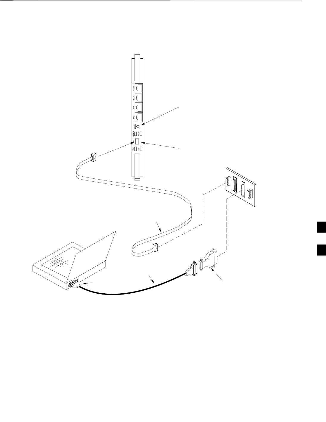
Using the LMF – continued
Jun 2004 1X SC480 BTS Hardware Installation, Optimization/ATP, and FRU 6-31
DRAFT
Figure 6-8: LMF Computer Common MMI Connections – Motorola MMI Interface Kit, SLN2006A
NULL MODEM
BOARD
(TRN9666A)
8–PIN TO 10–PIN
RS–232 CABLE
(P/N 30–09786R01)
RS–232 CABLE
8–PIN
LMF
COMPUTER
DB9–TO–DB25
ADAPTER
COM1
OR
COM2
FW00687
MMI
Connector
To MMI
Connector
RESET
Button
6
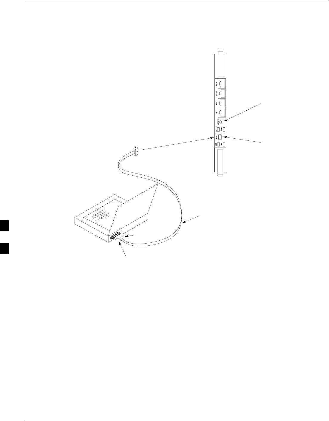
Using the LMF – continued
6-32 1X SC480 BTS Hardware Installation, Optimization/ATP, and FRU Jun 2004
DRAFT
FABRICATED MMI CABLE
(SEE MMI CABLE
FABRICATION APPENDIX D)
DB–9
CONNECTOR
8–PIN
LMF COMPUTER
OR EQUIVALENT
To MMI
Connector
COM1
OR
COM2
MMI
Connector
RESET
Button
Figure 6-9: MMI Connection Detail – Fabricated MMI Cable
Online Help
Task oriented online help is available in the LMF by clicking on Help in
the window menu bar, and selecting LMF Help from the pull–down
menu.
6
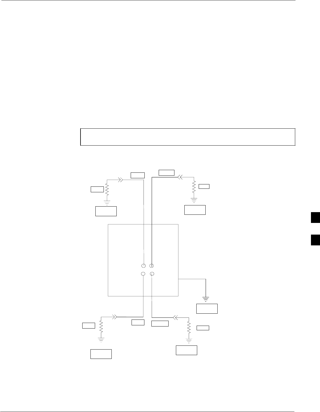
Pinging the Processors
JUN 2004 1X SC480 BTS Hardware Installation, Optimization/ATP, and FRU
DRAFT
6-33
Pinging the BTS
For proper operation, the integrity of the Ethernet LAN A and B links
must be verified. Figure 6-10 represents a typical BTS Ethernet
configuration. The drawing depicts cabling and termination for both the
A and B LANs.
Ping is a program that sends request data packets to hosts on a network,
in this case GLI modules on the BTS LAN, to obtain a response from the
“target” host specified by an IP address.
Follow the steps in Table 6-12 to ping each processor (on both LAN A
and LAN B) and verify LAN redundancy is working properly.
CAUTION Always wear an approved anti–static wrist strap while handling
any circuit card/module to prevent damage by ESD.
SIGNAL
GROUND
SIGNAL
GROUND
50Ω
BIN
SIGNAL
GROUND
50Ω
50Ω
SIGNAL
GROUND
50Ω
SIGNAL
GROUND
CHASSIS GROUND
TERMINATION TERMINATION
AIN
BOUT
AOUT
SC4812ETL0013–5
Figure 6-10: BTS Ethernet LAN Termination Diagram
TERMINATION
TERMINATION
6

Pinging the Processors
JUN 2004
1X SC480 BTS Hardware Installation, Optimization/ATP, and FRU
DRAFT
6-34
NOTE The Ethernet LAN A and B cables and/or terminations must be
installed on each frame/enclosure external LAN connector before
performing this test. All other processor board LAN connections
are made through the backplanes.
Table 6-12: Pinging the Processors
Step Action
1If this is a first–time communication with a newly–installed frame or a GLI card which has been
replaced, perform the procedure in Table 11-3 and then return to step 2.
2Be sure any uncabled LAN A and B IN and OUT connectors at the rear of BTS are terminated with 50
Ω loads.
3If it has not already been done, connect the LMF computer to the BTS.
4If it has not already been done, start a GUI LMF session and log into the BTS ( refer to Table 6-7).
5Remove the 50Ω termination on the BTS LAN B IN connector.
– The LMF session should remain active.
6Replace the 50Ω termination on the BTS LAN B IN connector.
7From the Windows desktop, click the Start button and select Run.
8In the Open box, type ping and the GLI IP address (for example, ping 128.0.0.2).
NOTE
128.0.0.2 is the default IP address for the GLI card in slot GLI–1 in field BTS units.
9Click on OK.
10 If the targeted module responds, a DOS window will appear with a display similar to the following:
Reply from 128.0.0.2: bytes=32 time=3ms TTL=255
– If the device responds, proceed to step 18.
If there is no response, the following is displayed:
Request timed out
– If the GLI fails to respond, it should be reset and re–pinged. If it still fails to respond, typical
problems would be: failure of the LMF to login, shorted BNC–to–inter-frame cabling, open
cables, crossed A and B link cables, or the GLI itself.
11 Logout of the BTS as described in Table 6-9, exit from the LMF program, and restart the Windows
operating system on the LMF computer.
12 Restart the LMF GUI program as described in LMF Help function on–line documentation, and log into
the BTS as described in Table 6-7.
13 Perform steps 7 through 10 again.
– If the device responds, proceed to step 18.
If there is still no response, proceed to step 14.
. . . continued on next page
6

Pinging the Processors
JUN 2004 1X SC480 BTS Hardware Installation, Optimization/ATP, and FRU
DRAFT
6-35
Table 6-12: Pinging the Processors
Step Action
14 If ping was unsuccessful after restarting the LMF computer, press the GLI front panel reset pushbutton
and perform steps 7 through 10 again.
15 After the BTS has been successfully pinged, be sure the 50Ω termination was replaced on the BTS
LAN B IN connector at the rear of the BTS. Disconnect the LMF cable from the front LAN A
connector, and connect it to front LAN B (right–hand connector).
16 Remove the 50Ω termination on the BTS LAN A IN connector.
17 Repeat steps 5 through 9 using LAN B.
18 After the BTS has been successfully pinged on the secondary LAN, replace the 50Ω termination on
the BTS LAN A IN connector.
19 Disconnect the LMF cable from the LAN B and connect it to LAN A.
20 Remove and replace the 50Ω termination on the LAN B IN connector to force the GLI to switch to
primary LAN A.
21 Repeat steps 5 through 9 to ensure proper primary LAN operation.
6

Download the BTS
6-36 1X SC480 BTS Hardware Installation, Optimization/ATP, and FRU Jun 2004
DRAFT
Overview
Before a BTS can operate, each equipped device must contain device
initialization (ROM) code. ROM code is loaded in all devices during
manufacture, factory repair, or, for software upgrades, from the CBSC
using the DownLoad Manager (DLM). Device application (RAM) code
and data must be downloaded to each equipped device by the user before
the BTS can be made fully functional for the site where it is installed.
ROM Code
Downloading ROM code to BTS devices from the LMF is NOT routine
maintenance or a normal part of the optimization process. It is only
done in unusual situations where the resident ROM code release level in
the device is not compatible with the required release level of the site
operating software and the CBSC can not communicate with the BTS to
perform the download.
If you must download ROM code, the procedures are located in
Appendix C.
Before ROM code can be downloaded from the LMF, the correct ROM
code file for each device to be loaded must exist on the LMF computer.
ROM code must be manually selected for download.
The ROM code file is not available for GLI3s. GLI3s are
ROM code loaded at the factory.
NOTE
ROM code can be downloaded to a device that is in any state. After the
download is started, the device being downloaded will change to
OOS_ROM (blue). The device will remain OOS_ROM (blue) when the
download is completed. A compatible revision–level RAM code must
then be downloaded to the device. Compatible code loads for ROM and
RAM must be used for the device type to ensure proper performance.
The compatible device code release levels for the Base Station System
(BSS) software release being used are listed in the Version Matrix
section of the SCt CDMA Release Notes (supplied on the tape or
CD–ROM containing the BSS software).
RAM Code
Before RAM code can be downloaded from the LMF, the correct RAM
code file for each device must exist on the LMF computer. RAM code
can be automatically or manually selected depending on the Device
menu item chosen and where the RAM code file for the device is stored
in the LMF file structure. The RAM code file will be selected
automatically if the file is in the <x>:\<lmf home
directory>\cdma\loads\n.n.n.n\code folder (where n.n.n.n is the
download code version number that matches the “NextLoad” parameter
of the CDF file). The RAM code file in the code folder must have the
correct hardware bin number for the device to be loaded.
6

Download the BTS – continued
Jun 2004 1X SC480 BTS Hardware Installation, Optimization/ATP, and FRU 6-37
DRAFT
RAM code can be downloaded to a device that is in any state. After the
download is started, the device being loaded will change to OOS_ROM
(blue). When the download is completed successfully, the device will
change to OOS_RAM (yellow).
When code is downloaded to a GLI, the LMF automatically also
downloads data and then enables the GLI. When enabled, the GLI will
change to INS_ACT (bright green).
For non–GLI devices, data must be downloaded after RAM code is
downloaded. To download data, the device state must be OOS_RAM
(yellow).
If an MCC–DO card is in use, it can only be loaded using the Local
Maintenance Tool (LMT). LMT is software designed specifically for the
MCC–DO card. To avoid confusion and duplication of effort, refer to
Motorola Lifecycles website at
http://www.motorola.com/networkoperators/CDMA–1xEV–DO.htm for
further information on LMT or MCC–DO.
The devices to be loaded with RAM code and data are:
SGroup Line Interface III (GLI3)
SClock Synchronization and Alarm card (CSA) (Only if new revision
code must be loaded)
SMulti–Channel CDMA (MCC–1X) cards
SBroad Band Transceiver (BBX–1X) cards
The GLI must be successfully downloaded with RAM code
and data, and in INS_ACT (bright green) status before
downloading any other device. The RAM code download
process for an GLI automatically downloads data and then
enables the GLI.
NOTE 6

Download the BTS – continued
6-38 1X SC480 BTS Hardware Installation, Optimization/ATP, and FRU Jun 2004
DRAFT
Verify GLI ROM Code Loads
Devices should not be loaded with a RAM code version which is not
compatible with the ROM code with which they are loaded. Before
downloading RAM code and data to the processor cards, follow the
procedure in Table 6-13 to verify the GLI devices are loaded with the
correct ROM code for the software release used by the Base Station
System.
Prerequisite
Identify the correct GLI ROM code load for the software release being
used on the BSS by referring to the Version Matrix section of the SCt
CDMA Release Notes (supplied on the tapes or CD–ROMs containing
the BSS software).
Table 6-13: Verify GLI ROM Code Loads
Step Action
1If it has not already been done, start a GUI LMF session and log into the BTS ( refer to Table 6-7).
2Select all GLI devices by clicking on them, and select Device > Status from the BTS menu bar.
3In the status report window which opens, note the number in the ROM Ver column for each GLI2.
4If the ROM code loaded in the GLIs is not the correct one for the software release being used on the
BSS, perform the following:
4a – Log out of the BTS as described in Table 6-9 or Table 6-10, as applicable.
4b – Disconnect the LMF computer.
4c – Reconnect the span lines as described in Table 8-6.
4d – Have the CBSC download the correct ROM code version to the BTS devices.
5When the GLIs have the correct ROM load for the software release being used, be sure the span lines
are disabled as outlined in Table 6-5 and proceed to downloading RAM code and data.
6

Download the BTS – continued
Jun 2004 1X SC480 BTS Hardware Installation, Optimization/ATP, and FRU 6-39
DRAFT
Download RAM Code and Data
to GLI
Prerequisites
SPrior to performing these procedures, ensure a code file exists for each
of the devices to be loaded.
SThe LMF computer is connected to the BTS (refer to Table 6-6), and
is logged in using the GUI environment (refer to Table 6-7).
Procedure
Follow the procedure in Table 6-14 to download the firmware
application code for GLI. The download code action downloads data and
also enables the GLI.
Table 6-14: Download and Enable GLI Device
nStep Action
1Note the active LAN to which the LMF computer is connected.
2At the rear of the BTS, remove the 50–ohm termination from the LAN OUT connector of the
LAN to which the LMF is not connected.
3 Select Tools > Update Next Load > CDMA function to ensure the Next Load parameter is set to
the correct code version level.
4Note the LAN IP address in the Network Login section of the LMF Login tab, and verify the Win
LMF is logged into the following IP address:
– GLI : 128.0.0.2
5Down load code to the GLI by clicking on the GLI.
– From the Device pull down menu, select Download > Code/Data
A status report confirms change in the device status.
– Click OK to close the status window. (The GLI should automatically be downloaded with
data and enabled.)
6If the card accepts the download and enables, proceed to step 8.
7If the BTS connection is lost during or after the download process, repeat step 4 and step 5 again.
8Re–install the 50 ohm termination removed from the LAN connector in step 2.
Download RAM Code and Data
to Non–GLI Devices
Downloads to non–GLI devices can be performed individually for each
device or all installed devices can be downloaded with one action.
6
Download the BTS – continued
6-40 1X SC480 BTS Hardware Installation, Optimization/ATP, and FRU Jun 2004
DRAFT
CSA devices are RAM code–loaded at the factory. RAM
code is downloaded to CSA only if a newer software
version needs to be loaded.
When downloading to multiple devices, the download may
fail for some of the devices (a time–out occurs). These
devices can be loaded individually after completing the
multiple download.
NOTE
Follow the steps in Table 6-15 to download RAM code and data to
non–GLI devices.
Table 6-15: Download RAM Code and Data to Non–GLI Devices
nStep Action
1Select the target CSA, MCC, and/or BBX device(s) by clicking on them.
2 Click Device in the BTS menu bar, and select Download > Code/Data in the pull–down menus.
– A status report is displayed that shows the results of the download for each selected device.
3 Click OK to close the status report window when downloading is completed.
NOTE
After a BBX, CSA, or MCC device is successfully loaded with RAM code and data have changed
to the OOS_RAM state (yellow), the status LED should be rapidly flashing GREEN.
NOTE
The command in Step 2 loads both code and data. Data can be downloaded without doing a code
download anytime a device is OOS–RAM using the command in Step 4.
4To download just the firmware application data to each device, select the target device and select:
Device>Download>Data
Selecting CSA Clock Source
and Enabling CSAs
CSA must be enabled prior to enabling the MCCs. Procedures in the
following two sub-sections cover the actions to accomplish this. For
additional information on the CSA sub–system, see “Clock
Synchronization and Alarm (CSA) in the CSA System Time – GPS &
HSO/MSO Verification section of this chapter.
Select CSA Clock Source
A CSA can have three different clock sources. The CSA Source function
can be used to select the clock source for each of the three inputs. This
function is only used if the clock source for a CSA needs to be changed.
The Clock Source function provides the following clock source options.
SLocal GPS
SRemote GPS
SHSO/MSO
6
Download the BTS – continued
Jun 2004 1X SC480 BTS Hardware Installation, Optimization/ATP, and FRU 6-41
DRAFT
Prerequisites
SGLI is INS_ACT (bright green)
SCSA is OOS_RAM (yellow) or INS_ACT (bright green)
Follow the procedure in Table 6-16 to select a CSA Clock Source.
Table 6-16: Select CSA Clock Source
nStep Action
1Select the CSA for which the clock source is to be selected.
2Click on Device in the BTS menu bar, and select CSA > Select Clock Source... in the pull–down
menu list.
– A CSA clock reference source selection window will appear.
3Select the applicable clock source in the Clock Reference Source pick lists. Uncheck the related
check boxes for Clock Reference Sources 2 and 3 if you do not want the displayed pick list item to
be used.
4Click on the OK button.
– A status report is displayed showing the results of the operation.
5Click on the OK button to close the status report window.
For Local GPS (RF–GPS), verify the CSA configured with
the GPS receiver “daughter board” is installed in the BTS’s
CSA slot before continuing.
NOTE
Enable CSA
Follow the steps outlined in Table 6-17 to enable the CSA.
Table 6-17: Enable CSA
nStep Action
1Click on Device in the BTS menu bar, and select Enable in the pull–down menu list.
– A status report is displayed showing the results of the enable operation.
– Click OK to close the status report window.
* IMPORTANT
– The GPS satellite system satellites are not in a geosynchronous orbit and are maintained and
operated by the United States Department of Defense (DOD). The DOD periodically alters
satellite orbits; therefore, satellite trajectories are subject to change. A GPS receiver that is INS
contains an “almanac” that is updated periodically to take these changes into account.
– If a GPS receiver has not been updated for a number of weeks, it may take up to an hour for the
GPS receiver “almanac” to be updated.
– Once updated, the GPS receiver must track at least four satellites and obtain (hold) a 3–D position
fix for a minimum of 45 seconds before the CSA will come in service. (In some cases, the GPS
receiver needs to track only one satellite, depending on accuracy mode set during the data load).
. . . continued on next page
6

Download the BTS – continued
6-42 1X SC480 BTS Hardware Installation, Optimization/ATP, and FRU Jun 2004
DRAFT
Table 6-17: Enable CSA
nActionStep
NOTE
– After CSA have been successfully enabled, be sure the STA/ALM LED is steady green
(alternating green/red indicates the card is in an alarm state).
2If more than an hour has passed without the CSA enabling, refer to the CSA System Time – GPS &
HSO/MSO Verification section of this chapter (see Table 6-19, Figure 6-11, and Table 6-20) to
determine the cause.
Enable MCCs
This procedure configures the MCC and sets the “tx fine adjust”
parameter. The “tx fine adjust” parameter is not a transmit gain setting,
but a timing adjustment that compensates for the processing delay in the
BTS (approximately 3 mS).
Follow the steps in Table 6-18 to enable the MCCs installed in the CCP2
shelf.
The GLI and primary CSA must be downloaded and
enabled (IN–SERVICE ACTIVE), prior to downloading
and enabling an MCC.
NOTE
Table 6-18: Enable MCCs
nStep Action
1If the GLI/MCC/BBX view is not displayed in the LMF window, click on the GLI/MCC/BBX area
of the CCP2 shelf.
2Click on the target MCC(s), or click on Select in the BTS menu bar, and select MCCs in the
pull–down menu list.
3Click on Device in the BTS menu bar, and select Enable in the pull–down menu list.
– A status report is displayed showing the results of the enable operation.
4 Click OK to close the status report window.
6

CSA System Time – GPS & HSO/MSO Verification
Jun 2004 1X SC480 BTS Hardware Installation, Optimization/ATP, and FRU 6-43
DRAFT
Clock Synchronization and
Alarm (CSA) Sub–system
Description
Overview
The primary function of the CSA card is to maintain CDMA system
time. A GPS receiver provides the primary timing reference for all
CDMA BTS’s During normal operation, the CSA clocking outputs are
phase locked to the GPS receiver timing reference. The CSA supports
either an on–board GPS receiver module (RF GPS) or Remote GPS
(RGPS) receiver. The RGPS receiver consists of a combined GPS
receiver and antenna witha digital interface to the CSA.
Backup Timing References
Timing signals from the High Stability Oscillator (HSO) or Medium
Stability Oscillator (MSO) are used in the event that the primary (GPS)
reference should become unavailable. The HSO or MSO clock is
calibrated against the GPS timing signal when a valid GPS timing signal
is available to provide the longest possible backup timing performance.
The CSA continuously monitors each available timing reference and
utilizes the most suited reference to maintain system synchronization.
Timing Source Fault Management
Fault management has the capability of switching between the GPS
synchronization source and the HSO/MSO backup source in the event of
a GPS receiver failure. During normal operation, the CSA selects GPS as
the primary timing source (Table 6-20). The source selection can also be
overridden via the WinLMF or by the system software.
Front Panel LEDs
The status of the LEDs on the CSA boards are as follows:
SSteady Green – CSA locked to GPS.
SRapidly Flashing Green – Standby CSA locked to GPS.
SFlashing Green/Rapidly Flashing Red – CSA OOS–RAM attempting
to lock on GPS signal.
SRapidly Flashing Green and Red – Alarm condition exists. Trouble
Notifications (TNs) are currently being reported to the GLI.
6

CSA System Time – GPS & HSO/MSO Verification – continued
6-44 1X SC480 BTS Hardware Installation, Optimization/ATP, and FRU Jun 2004
DRAFT
High Stability Oscillator /
Medium Stability Oscillator
(HSO/MSO)
General
CSA and HSO/MSO
The CSA utilizes timing signals provided by either an HSO or MSO to
maintain BTS synchronization during the absence of valid GPS timing
information. WHen a GPS timing signal is available the CSA is
responsible for calibration of the HSO or MSO clock to maximize the
backup timing interval. A minimum period of 24 hours of operation with
a valid GPS reference is required to fully calibrate the HSO backup
reference such that a 24 hour backup interval may be provided.
HSO
The HSO is a free–running backup oscillator that is capable of providing
a minimum backup interval of 24 hours.
MSO
The MSO is a free–running backup oscillator that is capable of providing
a minimum backup interval of 8 hours.
NOTE Allow the base site and test equipment to warm up for 60
minutes after any interruption in oscillator power. CSA card
warm-up allows the oscillator oven temperature and oscillator
frequency to stabilize prior to test. Test equipment warm-up
allows the Rubidium standard time base to stabilize in frequency
before any measurements are made.
6
CSA System Time – GPS & HSO/MSO Verification – continued
Jun 2004 1X SC480 BTS Hardware Installation, Optimization/ATP, and FRU 6-45
DRAFT
CSA Frequency Verification
The objective of this procedure is the initial verification of the Clock
Synchronization Alarms (CSA) Module before performing the RF path
verification tests.
Test Equipment Setup
(GPS & HSO/MSO Verification)
Follow the steps outlined in Table 6-19 to set up test equipment.
Table 6-19: Test Equipment Setup (GPS & HSO/MSO Verification)
Step Action
1Perform one of the following as required by installed equipment:
1a – Verify a CSA card is installed in the CSA slot, and that the card is INS_ACT (bright green).
2Connect a serial cable from the LMF COM 1 port (via null modem card) to the MMI port on the CSA
(see Figure 6-11).
3Start an MMI communication session with the CSA by using the Windows desktop shortcut icon (see
Table 6-11) .
4When the terminal screen appears press the Enter key until the CSA> prompt appears.
CAUTION If the RF GPS module is uesd to take care to ensure that the GPS
antenna is properly connected to the GPS antenna connector
within the power entry compartment only. Damage to the GPS
antenna and/or GPS receiver can result if the GPS antenna is
inadvertently connected to any other RF connector. 6
CSA System Time – GPS & HSO/MSO Verification – continued
6-46 1X SC480 BTS Hardware Installation, Optimization/ATP, and FRU Jun 2004
DRAFT
Figure 6-11: CSA MMI Terminal Connection
NULL MODEM
BOARD
(TRN9666A)
RS–232 SERIAL
MODEM CABLE
DB9–TO–DB25
ADAPTER
COM1
LMF
NOTEBOOK
FW00372
CSA card shown
removed from frame
FREQ. MONITOR
SYNC MONITOR
9–PIN TO 9–PIN
RS–232 CABLE
NOTES:
1. One LED on each CSA:
Green = IN–SERVICE ACTIVE
Fast Flashing Green = OOS–RAM
Red = Fault Condition
Flashing Green & Red = Fault
TO FRONT
PANEL
GPS Initialization/Verification
Prerequisites
Ensure the following prerequisites have been met before proceeding:
SThe CSA and HSO/MSO (if equipped) has been warmed up for at
least 15 minutes.
SThe LMF computer is connected to the MMI port of the CSA as
shown in Figure 6-11.
SAn MMI communication session has been started (Table 6-11), and
the CSA> prompt is present in the HyperTerminal window
(Table 6-19).
6

CSA System Time – GPS & HSO/MSO Verification – continued
Jun 2004 1X SC480 BTS Hardware Installation, Optimization/ATP, and FRU 6-47
DRAFT
Follow the steps outlined in Table 6-20 to initialize and verify proper
GPS receiver functioning.
Table 6-20: GPS Initialization/Verification
Step Action
1To verify that Clock alarms (0000), Dpll is locked and has a reference source, and
GPS self test passed messages are displayed within the report, issue the following MMI
command
bstatus
– The system will display a response similar to the following:
Clock Alarms (0000):
DPLL is locked and has a reference source.
GPS receiver self test result: passed
Time since reset 0:33:11, time since power on: 0:33:11
2Enter the following command at the CSA> prompt to display the current status of the GPS receiver and
HSO or MSO backup reference:
sources
– When equipped with HSO, the system will generate a response similar to the following:
N Source Name Type TO Good Status Last Phase Target Phase Valid
–––––––––––––––––––––––––––––––––––––––––––––––––––––––––––––––––––––––––
0LocalGPS Primary 4 YES Good 00Yes
1 HSO Backup 4 YES Good –2013177 –2013177 Yes
2 Not Used
*NOTE “Timed–out” should only be displayed while the HSO is warming up. If the HSO does not
appear as one of the sources, then configure the HSO as a back–up source by entering the following
command at the CSA> prompt:
ss 1 12
The HSO or MSO must complete an initial warmup and calibration cycle before being usable as a
backup reference source. The intial warmup cycle should be completed in less than 15 minutes. During
the warmup cycle, the HSO clock output is disabled and indicated as being “timed out” in the
following response to the “sources command:
43:26:15 CSA>sources
43:26:35
43:26:35 N Source Name Type TO Good Status Last Phase Target Phase Valid
43:26:35–––––––––––––––––––––––––––––––––––––––––––––––––––––––––––––––––––
43:26:35 0 Local GPS Primary 59 Yes Good 0 0 Yes
43:26:35 1 HSO Backup –25 No Bad timed out unknown No
43:26:35 2 Not Used
43:26:35 Current reference source number: 0
See 2–Cont.
. . . continued on next page
6

CSA System Time – GPS & HSO/MSO Verification – continued
6-48 1X SC480 BTS Hardware Installation, Optimization/ATP, and FRU Jun 2004
DRAFT
Table 6-20: GPS Initialization/Verification
Step Action
2–
Cont At the completion of the HSO warmup cycle, the HSO clcok output is enabled allowing califd clock
pulses to be detected by the CSA. An integer value should then be displayed in the HSO “Last Phase”
entry of the “sources” command as show below. If the HSO or MSO calibration cycle is not completed
within 2 hours it will be necessary to inspect the HSO or MSO hardware.
43:29:33 CSA>sources
43:29:43
43:29:43 N Source Name Type TO Good Status Last Phase Target Phase Valid
43:29:43 ––––––––––––––––––––––––––––––––––––––––––––––––––––––––––––––––
43:29:43 0 Local GPS Primary 59 Yes Good 0 0 Yes
43:29:43 1 HSO Backup 3 Yes Bad –xxxxxx –xxxxxx No
43:29:43 2 Not Used
43:29:43 Current reference source number: 0
The HSO or MSO calibration cycle can take as long as 2 hours to complete. The completion of the
HSO or MSO calibration is indicated by a “yes” value in the valid column of the “sources” command
response as shown below. If the HSO or MSO calibration cycle is not complete within 2 hours it will
be necessary to inspect the HSO or MSO hardware.
26:09:33 CSA>sources
26:09:35
26:09:35 N Source Name Type TO Good Status Last Phase Target Phase Valid
26:09:35 ––––––––––––––––––––––––––––––––––––––––––––––––––––––––––––––––
26:09:35 0 Local GPS Primary 59 Yes Good 0 0 Yes
26:09:35 1 HSO Backup 3 Yes Bad 8683466 8683466 Yes
26:09:35 2 Not Used
26:09:35 Current reference source number: 0
3HSO information (underlined text above, verified from left to right) is usually the #1 reference source.
If this is not the case, have the OMC–R determine the correct BTS timing source has been identified in
the database by entering the display bts csmgen command and correct as required using the edit
csm csmgen refsrc command.
NOTE
If any of the above areas fail, verify:
– Verify that HSO had been powered up for at least 15 minutes.
– If “timed out” is displayed in the Last Phase column, suspect the HSO output buffer or oscillator
is defective
– Verify the HSO is FULLY SEATED and LOCKED.
4Verify the following GPS information (underlined text above):
– GPS information is usually the 0 reference source.
– At least one Primary source must indicate “Status = good” and “Valid = yes” to bring site up.
. . . continued on next page
6

CSA System Time – GPS & HSO/MSO Verification – continued
Jun 2004 1X SC480 BTS Hardware Installation, Optimization/ATP, and FRU 6-49
DRAFT
Table 6-20: GPS Initialization/Verification
Step Action
5Enter the following command at the CSA> prompt to verify that the GPS receiver is in tracking mode.
gstatus
– Observe the following typical response:
27:27:11 CSA>gstatus
27:27:14 GPS Receiver Control Task State: tracking satellites.
27:27:14 Time since last valid fix: 0 seconds
27:27:14 Frame type (0): master
27:27:14
27:27:14 Recent Change Data:
27:27:14 GPS time offset 0 ns.
27:27:14 Initial position: lat 151679000 msec, lon: –316798000 msec, height 0 cm
(GPS)
27:27:14 Initial position accuracy (0): estimated.
27:27:14
27:27:14 GPS Receiver Status
27:27:14 Position hold: lat 151679326 msec, lon: –316798498 msec, hgt 21955 cm
27:27:14 Current position: lat 151679326 msec, lon: –316798498 msec, hgt 21955 cm
(GPS)
27:27:14 8 satellites tracked, receiving 8 satellites, 8 satellites visible.
27:27:14 Current Dilution of Precision (PDOP or HDOP): 0
27:27:14 Date & Time: 2004:03:16:21:37:48 LS:13
27:27:14 GPS Receiver Status Byte:0x8400
27:27:14 Chan:0, SVID: 24, Mode: 8, RSSI: 42, Status: 0x08a1
27:27:14 Chan:1, SVID: 10, Mode: 8, RSSI: 49, Status: 0x08a0
27:27:14 Chan:2, SVID: ––, Mode: –, RSSI: –––, Status: 0x0000
27:27:14 Chan:3, SVID: 21, Mode: 8, RSSI: 48, Status: 0x08a1
27:27:14 Chan:4, SVID: 26, Mode: 8, RSSI: 50, Status: 0x08a0
27:27:14 Chan:5, SVID: 29, Mode: 8, RSSI: 48, Status: 0x08a0
27:27:14 Chan:6, SVID: 18, Mode: 8, RSSI: 42, Status: 0x08a0
27:27:14 Chan:7, SVID: 17, Mode: 8, RSSI: 50, Status: 0x08a0
27:27:14 Chan:8, SVID: 6, Mode: 8, RSSI: 49, Status: 0x08a0
27:27:14 Chan:9, SVID: ––, Mode: –, RSSI: –––, Status: 0x0000
27:27:14 Chan:10, SVID: ––, Mode: –, RSSI: –––, Status: 0x0000
27:27:14 Chan:11, SVID: ––, Mode: –, RSSI: –––, Status: 0x0000
27:27:14
6Verify the following GPS information (shown above in underlined text):
– At least 4 satellites are tracked, and 4 satellites are visible.
– GPS Receiver Control Task State is “tracking satellites”. Do not continue until this occurs!
– Dilution of Precision indication is not more that 30.
Record the current position base site latitude, longitude, height and height reference (height reference
to Mean Sea Level (MSL) or GPS height (GPS). (GPS = 0 MSL = 1).
. . . continued on next page
6

CSA System Time – GPS & HSO/MSO Verification – continued
6-50 1X SC480 BTS Hardware Installation, Optimization/ATP, and FRU Jun 2004
DRAFT
Table 6-20: GPS Initialization/Verification
Step Action
7If steps 1 through 6 pass, the GPS is good.
NOTE
If any of the above mentioned areas fail, verify that:
– If Initial position accuracy is “estimated” (typical), at least 4 satellites must be tracked and
visible (1 satellite must be tracked and visible if actual lat, log, and height data for this site has
been entered into CDF file).
– If Initial position accuracy is “surveyed,” position data must be of sufficient accuracy or
improper GPS receiver timing may occur.
– The GPS antenna is not obstructed or misaligned.
– GPS antenna connector center conductor measureS approximately +5 Vdc with respect to the
shield.
– There is no more than 15 dB of loss between the GPS antenna OSX connector and the BTS frame
GPS input.
– Any lightning protection installed between GPS antenna and BTS frame is installed correctly.
8Enter the following commands at the CSA> prompt to verify that the CSA is warmed up and that GPS
acquisition has taken place.
debug dpllp
Observe the following typical response if the CSA is not warmed up (15 minutes from application of
power) (If warmed–up proceed to step 9)
CSA>DPLL Task Wait. 884 seconds left.
DPLL Task Wait. 882 seconds left.
DPLL Task Wait. 880 seconds left. ...........etc.
NOTE
The warm command can be issued at the MMI port used to force the CSA into warm–up, but the
reference oscillator will be unstable.
9Observe the following typical response if the CSA is warmed up.
c:17486 off: –11, 3, 6 TK SRC:0 S0: 3 S1:–2013175,–2013175
c:17486 off: –11, 3, 6 TK SRC:0 S0: 3 S1:–2013175,–2013175
c:17470 off: –11, 1, 6 TK SRC:0 S0: 1 S1:–2013175,–2013175
c:17486 off: –11, 3, 6 TK SRC:0 S0: 3 S1:–2013175,–2013175
c:17470 off: –11, 1, 6 TK SRC:0 S0: 1 S1:–2013175,–2013175
c:17470 off: –11, 1, 6 TK SRC:0 S0: 1 S1:–2013175,–2013175
10 Verify the following GPS information (underlined text above, from left to right):
– Lower limit offset from tracked source variable is not less than –60 (equates to 3µs limit).
– Upper limit offset from tracked source variable is not more than +60 (equates to 3µs limit).
– TK SRC: 0 is selected, where SRC 0 = GPS.
11 Enter the following commands at the CSA> prompt to exit the debug mode display.
debug dpllp
6

Test Equipment Setup
Jun 2004 1X SC480 BTS Hardware Installation, Optimization/ATP, and FRU 6-51
DRAFT
Connecting Test Equipment to
the BTS
The following types of test equipment are required to perform calibration
and ATP tests:
SWinLMF
SCommunications system analyzer model supported by the WinLMF
SPower meter model supported by the WinLMF (required when using
the HP 8921A/600 and Advantest R3465 analyzers)
SNon–radiating transmit line termination load
SDirectional coupler and in–line attenuator
SRF cables and adapters
Refer to Table 6-21 for an overview of connections for test equipment
currently supported by the WinLMF. In addition, see the following
figures:
SFigure 6-15, Figure 6-17, and Figure 6-18 show the test set
connections for TX calibration
SFigure 6-19 through Figure 6-22 show the test set connections for
optimization/ATP tests
Test Equipment GPIB Address
Settings
All test equipment is controlled by the WinLMF through an
IEEE–488/GPIB bus. To communicate on the bus, each piece of test
equipment must have a GPIB address set which the WinLMF will
recognize. The standard address settings used by the WinLMF for the
various types of test equipment items are as follows:
SSignal generator address: 1
SPower meter address: 13
SCommunications system analyzer: 18
Using the procedures included in the Verifying and Setting GPIB
Addresses section of Appendix B, verify and, if necessary, change the
GPIB address of each piece of employed test equipment to match the
applicable addresses above.
Supported Test Equipment
CAUTION To prevent damage to the test equipment in high power
configurations, all transmit (TX) test connections must be
through a 30 dB directional coupler plus a 20 dB in-line
attenuator for the 800 MHz BTSs.
Attenuators are not required for low power configurations.
IS–95A/B Operation
Optimization and ATP testing for IS–95A/B sites or carriers may be
performed using the following test equipment:
6

Test Equipment Setup – continued
6-52 1X SC480 BTS Hardware Installation, Optimization/ATP, and FRU Jun 2004
DRAFT
SCyberTest (High Power Configurations only)
SAdvantest R3267 spectrum analyzer with R3562 signal generator
SAdvantest R3465 spectrum analyzer with R3561L signal generator
and HP–437B or Gigatronics Power Meter
SAgilent E4406A transmitter test set with E4432B signal generator
SAgilent 8935 series E6380A communications test set (formerly HP
8935)
SHewlett–Packard HP 8921 (with CDMA interface and, for 1.9 GHz,
PCS Interface) and HP–437B or Gigatronics Power Meter
SSpectrum Analyzer (HP8594E) – optional
SRubidium Standard Timebase – optional
CDMA2000 1X Operation
Optimization and ATP testing for CDMA2000 1X sites or carriers may
be performed using the following test equipment:
SAdvantest R3267 spectrum analyzer with R3562 signal generator
SAgilent E4406A transmitter test set with E4432B signal generator
SAgilent 8935 series E6380A communications test set (formerly HP
8935) with option 200 or R2K and with E4432B signal generator for
1X FER
SAgilent E7495A communications test set
Test Equipment Preparation
See Appendix B for specific steps to prepare each type of test set and
power meter to perform calibration and ATP.
Agilent E7495A communications test set requires additional setup and
preparation. This is described in detail in Appendix B.
6
Test Equipment Setup – continued
Jun 2004 1X SC480 BTS Hardware Installation, Optimization/ATP, and FRU 6-53
DRAFT
Test Equipment Connection
Charts
To use the following charts to identify necessary test equipment
connections, locate the communications system analyzer being used in
the COMMUNICATIONS SYSTEM ANALYZER columns, and read down
the column. Where a dot appears in the column, connect one end of the
test cable to that connector. Follow the horizontal line to locate the end
connection(s), reading up the column to identify the appropriate
equipment and/or BTS connector.
IS–95A/B–only Test Equipment Connections
Table 6-21 depicts the interconnection requirements for currently
available test equipment supporting IS–95A/B only which meets
Motorola standards and is supported by the WinLMF.
Table 6-21: IS–95A/B–only Test Equipment Interconnection
COMMUNICATIONS SYSTEM ANALYZER ADDITIONAL TEST EQUIPMENT
SIGNAL Cyber–Test Advantest
R3465 HP 8921A HP 8921
W/PCS Power
Meter GPIB
Interface WinL
MF
Attenuator
&
Directional
Coupler BTS
EVEN SECOND
SYNCHRONIZATION EVEN
SEC REF EVEN SEC
SYNC IN
EVEN
SECOND
SYNC IN
EVEN
SECOND
SYNC IN
19.6608 MHZ
CLOCK TIME
BASE IN
CDMA
TIME BASE
IN
CDMA
TIME BASE
IN
CDMA
TIME BASE
IN
CONTROL
IEEE 488 BUS IEEE
488 GPIB GPIB SERIAL
PORT
HP–I
BHP–IB
TX TEST
CABLES RF
IN/OUT INPUT
50WTX1–6
RF
IN/OUT RF
IN/OUT 20 DB
ATTEN. BTS
PORT
RX TEST
CABLES RF
GEN OUT RF OUT
50WRX1–6
DUPLEX
OUT RF OUT
ONLY
SYNC
MON-
ITOR
FREQ
MON-
ITOR
HP–IB
6
Test Equipment Setup – continued
6-54 1X SC480 BTS Hardware Installation, Optimization/ATP, and FRU Jun 2004
DRAFT
CDMA2000 1X/IS–95A/B–capable Test Equipment
Connections
Table 6-22 depicts the interconnection requirements for currently
available test equipment supporting both CDMA 2000 1X and
IS–95A/B which meets Motorola standards and is supported by the
WinLMF.
Table 6-22: CDMA2000 1X/IS–95A/B Test Equipment Interconnection
COMMUNICATIONS SYSTEM ANALYZER ADDITIONAL TEST EQUIPMENT
SIGNAL
Agilent
8935 (Op-
tion 200
or R2K) Agilent
E7495A
Advan
test
R3267 Agilent
E4406A
Agilent
E4432B
Signal
Generator
Advant-
est
R3562
Signal
Genera-
tor Power
Meter
GPIB
Inter-
face WinL
MF
30 dB
Directional
Coupler &
20 dB Pad* BTS
EVEN SECOND
SYNCHRONIZATION EXT
TRIG IN EXT
TRIG TRIGGER
IN
19.6608 MHZ
CLOCK MOD TIME
BASE IN EXT REF
IN
CONTROL
IEEE 488 BUS IEEE
488 GPIB HP–IB GPIB SERIAL
PORT
HP–IB
TX TEST
CABLES RF
IN/OUT RF IN TX1–6
RF INPUT
50 OHM 30 DB COUPLER
AND 20 DB PAD
RX TEST
CABLES RF OUT
50 OHM
RF OUT
50–OHM RX1–6
RF OUT
ONLY
SYNC
MONI
TOR
FREQ
MONITOR
PATTERN
TRIG IN
GPIB
RF OUTPUT
50 OHM
RF OUTPUT
50–OHM
10 MHZ IN 10 MHZ OUT
(SWITCHED) 10 MHZ IN
10 MHZ
OUT
10 MHZ
SERIAL
I/O SERIAL
I/O
SIGNAL SOURCE
CONTROLLED
SERIAL I/O
EVEN
SECOND
SYNC IN
EXT REF
IN
HP–IB
RF IN/OUT
DUPLEX
OUT *
SYNTHE
REF IN
* WHEN USED ALONE, THE AGILENT 8935 WITH OPTION 200 OR R2K SUPPORTS IS–95A/B RX TESTING BUT NOT CDMA2000 1X RX TESTING.
EVEN
SECOND
SYNC IN
PORT 1
RF OUT
PORT 2
RF IN
6
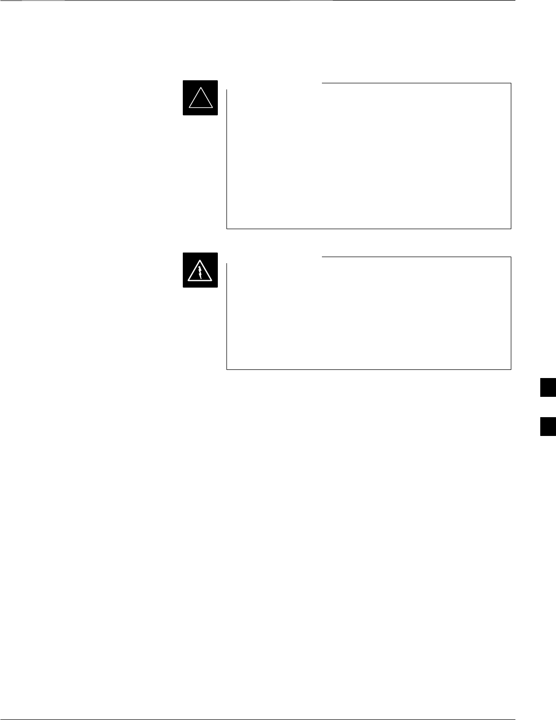
Test Equipment Setup – continued
Jun 2004 1X SC480 BTS Hardware Installation, Optimization/ATP, and FRU 6-55
DRAFT
Equipment Warm-up
Warm-up BTS equipment for a minimum of 60 minutes
prior to performing the BTS optimization procedure. This
assures BTS stability and contributes to optimization
accuracy.
– Agilent E7495A for a minimum of 30 minutes
– All other test sets for a minimum of 60 minutes
– Time spent running initial or normal power-up,
hardware/firmware audit, and BTS download counts
as warm-up time.
IMPORTANT
*
Before installing any test equipment directly to any BTS
TX OUT connector, verify there are no CDMA channels
keyed.
– At active sites, have the OMC-R/CBSC place the
antenna (sector) assigned to the BBX under test OOS.
Failure to do so can result in serious personal injury
and/or equipment damage.
WARNING
Automatic Cable Calibration
Set–up
Figure 6-21 and Figure 6-22 show the cable calibration setup for the test
sets supported by the WinLMF. The left side of the diagram depicts the
location of the input and output connectors of each test equipment item,
and the right side details the connections for each test. Table 6-24
provides a procedure for performing automatic cable calibration.
Manual Cable Calibration
If manual cable calibration is required, refer to the procedures in
Appendix B.
6
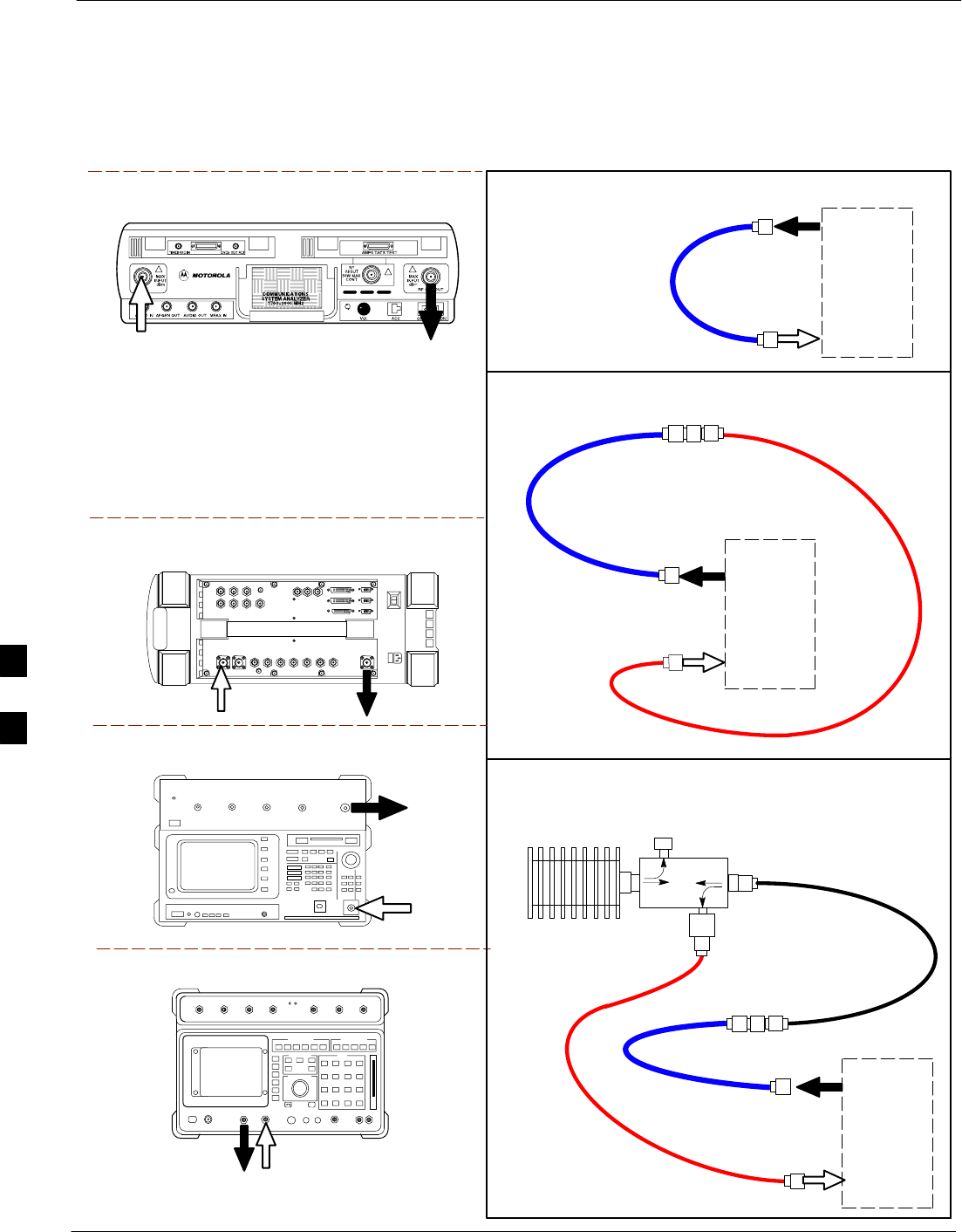
Test Equipment Setup – continued
6-56 1X SC480 BTS Hardware Installation, Optimization/ATP, and FRU Jun 2004
DRAFT
Motorola CyberTest
Advantest Model R3465
RF OUT 50Ω
INPUT 50Ω
RF GEN OUTANT IN
SUPPORTED TEST SETS
100–WATT (MIN)
NON–RADIATING
RF LOAD
TEST
SET
A. SHORT CABLE CAL
SHORT
CABLE
B. RX TEST CAL SETUP
TEST
SET
C. TX TEST AND RX TEST CAL SETUP
20 DB IN–LINE
ATTENUATOR
CALIBRATION SET UP
N–N FEMALE
ADAPTER
TX
CABLE
SHORT
CABLE
Note: The 30 dB directional coupler is not used
with the Cybertest test set. The TX cable is
connected directly to the Cybertest test set.
A 10dB attenuator must be used with the short test
cable for cable calibration with the CyberTest test
set. The 10dB attenuator is used only for the cable
calibration procedure, not with the test cables for
TX calibration and ATP tests.
TEST
SET
RX
CABLE
SHORT
CABLE
DIRECTIONAL
COUPLER
(30 DB)
N–N FEMALE
ADAPTER
50 Ω
ΤERM.
Figure 6-12: IS–95A/B and CDMA 2000 1X Cable Calibration Test Setup –
Agilent E4406A/E4432B and Advantest R3267/R3562
Agilent 8935 Series E6380A
(formerly HP 8935)
RF
IN/OUT
ANT
IN
Hewlett Packard Model HP 8921A
Note: For 800 MHZ only. The HP8921A cannot
be used to calibrate cables for PCS frequencies.
TX CABLE FOR
TX TEST CABLE
CALIBRATION
RX CABLE FOR
DRDC RX TEST
CABLE CALIBRATION
DUPLEX
OUT ANT
IN
6
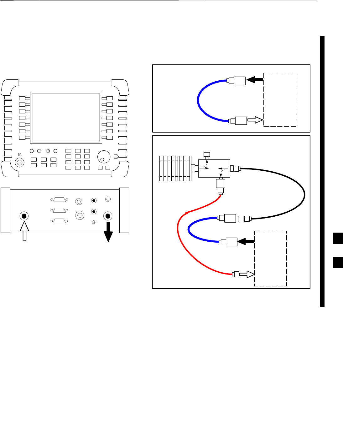
Test Equipment Setup – continued
Jun 2004 1X SC480 BTS Hardware Installation, Optimization/ATP, and FRU 6-57
DRAFT
TEST
SET
A. SHORT CABLE CAL
SHORT
CABLE
CALIBRATION SET UP
100–WATT (MIN)
NON–RADIATING
RF LOAD
D. RX and TX TEST SETUP
20 DB IN–LINE
ATTENUATOR
N–N FEMALE
ADAPTER
TX
CABLE
DIRECTIONAL
COUPLER
(30 DB)
50 Ω
ΤERM.
TX CABLE FOR
TX TEST CABLE
CALIBRATION
RX CABLE FOR
DRDC RX TEST
CABLE CALIBRATION
10 DB PAD
10 DB PAD
SHORT
CABLE
10 DB PAD
10 DB PAD
TEST
SET
SUPPORTED TEST SETS
Agilent E7495A
PORT 1
RF OUT
PORT 2
RF IN
Use only
Agilent supplied
power adapter
GPS
GPIO
Serial 1
Serial 2
Power REF
50 MHz
Sensor
Ext Ref
In
Even Second
Sync In
Antenna
Port 1
RF Out / SWR
Port 2
RF In
Figure 6-13: CDMA2000 1X Cable Calibration Test Setup – Agilent E7495A
6
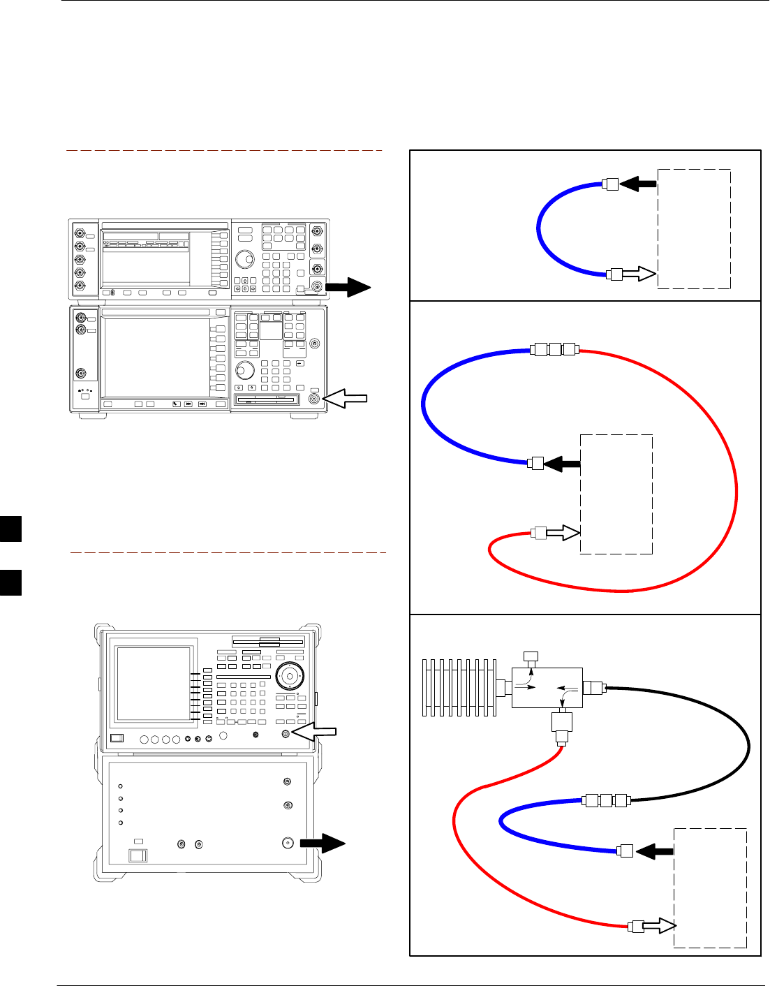
Test Equipment Setup – continued
6-58 1X SC480 BTS Hardware Installation, Optimization/ATP, and FRU Jun 2004
DRAFT
TEST
SET
A. SHORT CABLE CAL
SHORT
CABLE
B. RX TEST SETUP
CALIBRATION SET UP
TEST
SET
RX
CABLE
SHORT
CABLE
N–N FEMALE
ADAPTER
Figure 6-14: IS–95A/B and CDMA 2000 1X Cable Calibration Test Setup – Agilent E4406A/E4432B
and Advantest R3267/R3562
SUPPORTED TEST SETS
INPUT 50 Ω
RF OUT
50 Ω
Advantest R3267 (Top) and R3562 (Bottom)
NOTE:
SYNTHE REF IN ON REAR OF SIGNAL GENERATOR IS
CONNECTED TO 10 MHZ OUT ON REAR OF SPECTRUM
ANALYZER
Agilent E4432B (Top) and E4406A (Bottom)
NOTE:
10 MHZ IN ON REAR OF SIGNAL GENERATOR IS CONNECTED TO
10 MHZ OUT (SWITCHED) ON REAR OF TRANSMITTER TESTER
(FIGURE B-18).
RF INPUT
50 Ω
RF OUTPUT
50 Ω
100–WATT (MIN)
NON–RADIATING
RF LOAD
TEST
SET
D. TX TEST SETUP AND RX TEST SETUP
20 DB IN–LINE
ATTENUATOR
N–N FEMALE
ADAPTER
TX
CABLE
SHORT
CABLE
DIRECTIONAL
COUPLER
(30 DB)
50 Ω
ΤERM.
TX CABLE FOR
TX TEST CABLE
CALIBRATION
RX CABLE FOR
DRDC RX TEST
CABLE CALIBRATION
6
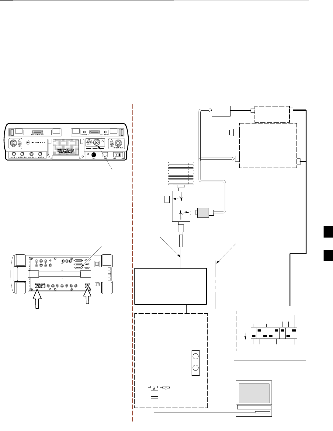
Test Equipment Setup – continued
Jun 2004 1X SC480 BTS Hardware Installation, Optimization/ATP, and FRU 6-59
DRAFT
Set-up for TX Calibration
Figure 6-15 and Figure 6-17 show the test set connections for TX
calibration.
Figure 6-15: TX Calibration Test Setup –
CyberTest (IS–95A/B) and Agilent 8935 (IS–95A/B and CDMA2000 1X)
Motorola CyberTest
Agilent 8935 Series E6380A (formerly HP 8935)
TEST SETS TRANSMIT (TX) SET UP
FRONT PANEL RF
IN/OUT
RF
IN/OUT
HP–IB
TO GPIB
BOX
NOTE: THE 30 DB DIRECTIONAL COUPLER IS NOT
USED WITH THE CYBERTEST TEST SET. THE TX
CABLE IS CONNECTED DIRECTLY TO THE
CYBERTEST TEST SET.
RS232–GPIB
INTERFACE BOX
GPIB
CABLE
RS232 NULL
MODEM
CABLE
S MODE
DATA FORMAT
BAUD RATE
GPIB ADRS G MODE
ON
BTS
CDM
WinLMF
DIP SWITCH SETTINGS
LAN
B
LAN
A
GPIB
RF IN/OUT
FREQ
MONITOR
SYNC
MONITOR
CSA
Communications
System Analyzer
0–20 DB
IN–LINE
ATTENUATOR
50 Ω
TERM
.
TX TEST
CABLE
DIRECTIONAL
COUPLER
(30 DB)
100–WATT (MIN.)
NON–RADIATING
RF LOAD
TX TEST
CABLE
* BLACK RECTANGLES
REPRESENT THE RAISED
PART OF SWITCHES
Power Meter
(OPTIONAL)*
POWER
SENSOR
* A POWER METER CAN BE USED IN
PLACE OF THE COMMUNICATIONS
TEST SET FOR TX CALIBRATION/
AUDIT
NOTE:
TO PERFORM LOW POWER CALIBRATION
THE POWER METER IS ADEQUATE FOR
MEASUREMENT PURPOSES WITHOUT
USING THE 30 DB DIRECTIONAL COUPLER
AND 0–20 DB ATTENUATOR.
IF THE AGILENT 8935 MUST BE USED,
THEN CONNECT TO THE ANT IN PORT.
ANT
IN
cCLPA
ANTENNA
CONNECTOR
TX IN
CONNECTOR
RX OUT
CONNECTOR
TX 1RX DIV
LOW POWER
CONNECTION
HIGH POWER
CONNECTION
6
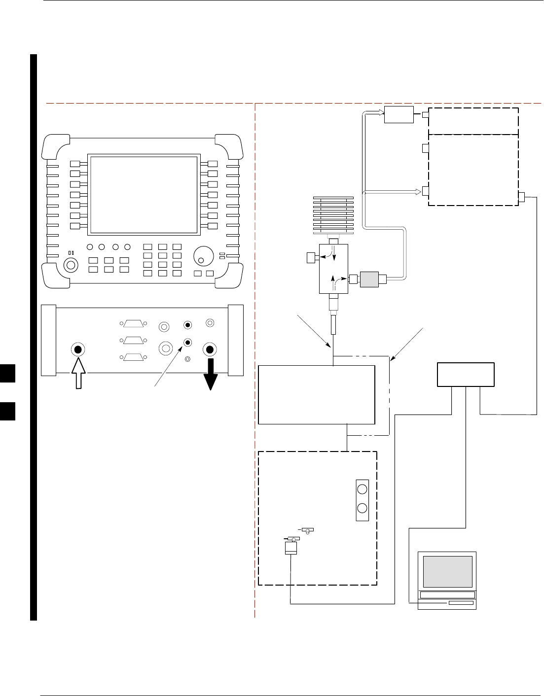
Test Equipment Setup – continued
6-60 1X SC480 BTS Hardware Installation, Optimization/ATP, and FRU Jun 2004
DRAFT
TEST SETS TRANSMIT (TX) SET UP
BTS CDMA
WinLMF
10BASET/
10BASE2
CONVERTER
LAN
B
LAN
A
RX DIV
SYNC
MONITOR
CSA
TX 1
50 Ω
TERM
.
TX TEST
CABLE
DIRECTIONAL
COUPLER
(30 DB)
100–WATT (MIN.)
NON–RADIATING
RF LOAD
TX TEST
CABLE
NOTE: IF BTS IS EQUIPPED
WITH DUPLEXED RX/TX
SIGNALS, CONNECT THE TX
TEST CABLE TO THE
DUPLEXED ANTENNA
CONNECTOR.
POWER
SENSOR
2O DB IN–LINE
ATTENUATOR
ETHERNET HUB
UNIVERSAL TWISTED PAIR (UTP)
CABLE (RJ45 CONNECTORS)
Agilent E7495A
PORT 1
RF OUT
PORT 2
RF IN
SYNC MONITOR
EVEN SEC TICK
PULSE REFERENCE
FROM CSM BOARD
Use only
Agilent supplied
power adapter
GPS
GPIO
Serial 1
Serial 2
Power REF
50 MHz
Sensor
Ext Ref
In
Even Second
Sync In
Antenna
Port 1
RF Out / SWR
Port 2
RF In
INTERNAL
ETHERNET
CARD
COMMUNICATIONS
system analyzer
POWER METER
PORT 2
RF IN
PORT 1
RF OUT
FREQ
MONITOR
Figure 6-16: TX Calibration Test Setup – Agilent E7495A (IS–95A/B and CDMA2000 1X)
ANTENNA
CONNECTOR
RX OUT
CONNECTOR
TX IN
CONNECTOR
HIGH POWER
CONNECTION
LOW POWER
CONNECTION
6
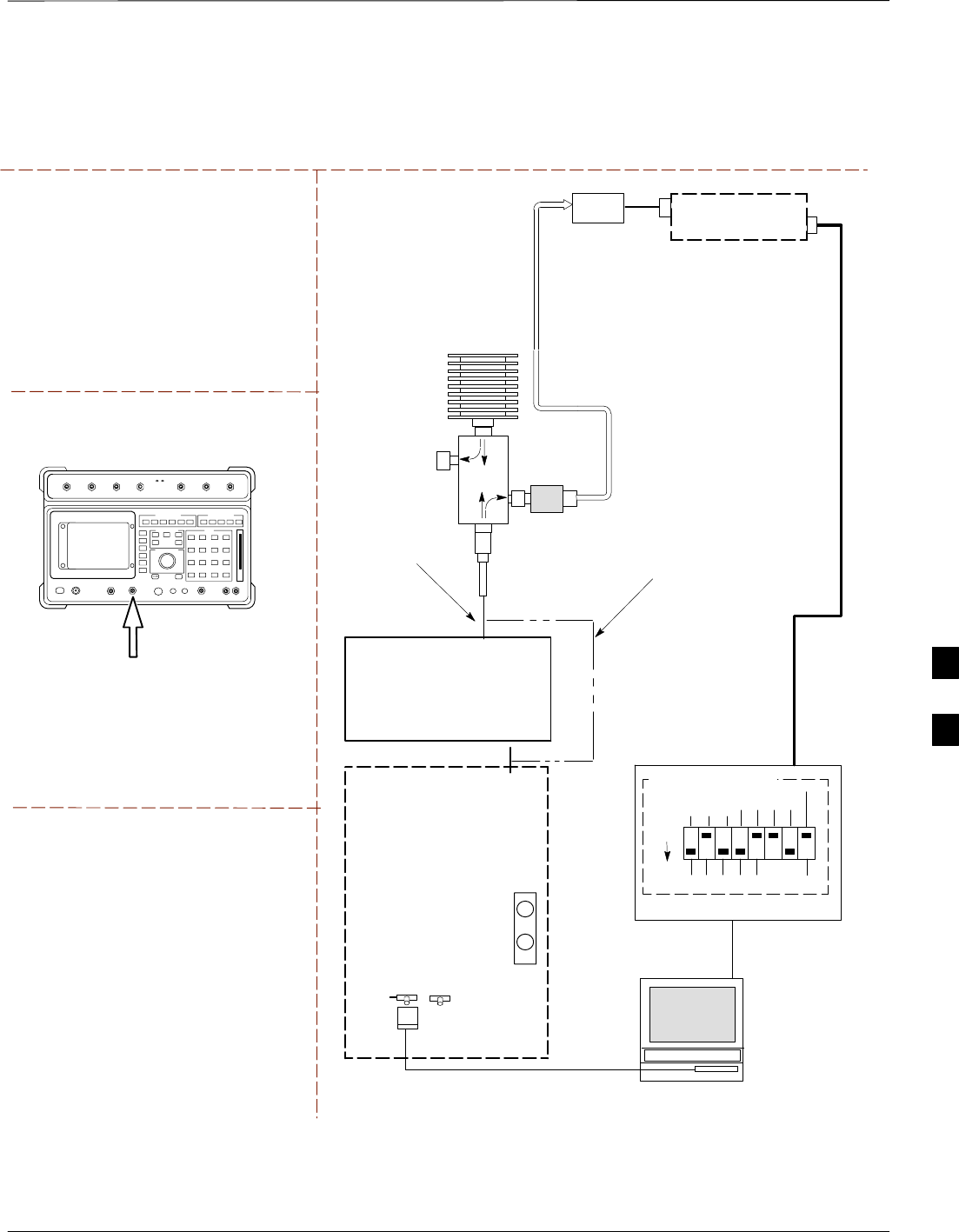
Test Equipment Setup – continued
Jun 2004 1X SC480 BTS Hardware Installation, Optimization/ATP, and FRU 6-61
DRAFT
TEST SETS TRANSMIT (TX) SET UP
NOTE:
THE HP8921A AND ADVANTEST R3465
CANNOT BE USED FOR TX CALIBRATION. A
POWER METER MUST BE USED.
RS232–GPIB
INTERFACE BOX
GPIB
CABLE
RS232 NULL
MODEM
CABLE
S MODE
DATA FORMAT
BAUD RATE
GPIB ADRS G MODE
ON
BTS
CDMA
WinLMF
DIP SWITCH SETTINGS
LAN
B
LAN
A
FREQ
MONITOR
SYNC
MONITOR
CSA
50 Ω
TERM
.
TX TEST
CABLE
DIRECTIONAL
COUPLER
(30 DB)
100–WATT (MIN.)
NON–RADIATING
RF LOAD
TX TEST
CABLE
* BLACK RECTANGLES
REPRESENT THE RAISED
PART OF SWITCHES
POWER
SENSOR Power Meter
0–20 DB IN–LINE
ATTENUATOR
NOTE:
TO PERFORM LOW POWER CALIBRATION
THE 30 DB DIRECTIONAL COUPLER AND
0–20 DB ATTENUATOR ARE NOT REQUIRED.
ANT
IN
Hewlett Packard Model HP 8921A
(for 800 MHz)
NOTE:
TO PERFORM LOW POWER CALIBRATION
USING THE HP8921A, CONNECT TO THE
ANT IN PORT. THE 30 DB DIRECTIONAL
COUPLER AND 0–20 DB ATTENUATOR ARE
NOT REQUIRED.
cCLPA
ANTENNA
CONNECTOR
TX IN
CONNECTOR
RX OUT
CONNECTOR
TX 1RX DIV
LOW POWER
CONNECTION
HIGH POWER
CONNECTION
Figure 6-17: TX Calibration Test Setup – Using Power Meter
6
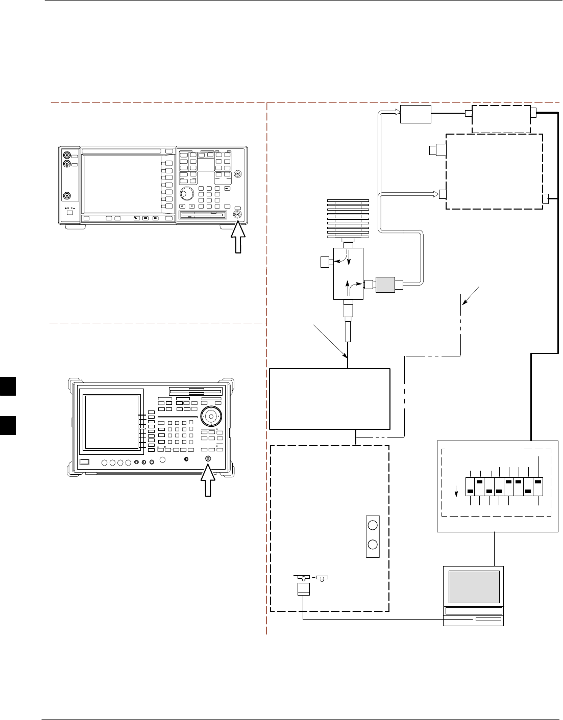
Test Equipment Setup – continued
6-62 1X SC480 BTS Hardware Installation, Optimization/ATP, and FRU Jun 2004
DRAFT
Figure 6-18: TX Calibration Test Setup –
Agilent E4406A and Advantest R3567 (IS–95A/B and CDMA2000 1X)
TEST SETS TRANSMIT (TX) SET UP
RS232–GPIB
INTERFACE BOX
GPIB
CABLE
RS232 NULL
MODEM
CABLE
S MODE
DATA FORMAT
BAUD RATE
GPIB ADRS G MODE
ON
BTS
CDMA
WinLMF
DIP SWITCH SETTINGS
LAN
B
LAN
A
GPIB
RF INPUT 50 Ω
OR INPUT 50 Ω
FREQ
MONITOR
SYNC
MONITOR
CSA
Communications
SystemAanalyzer
50 Ω
TERM
.
TX TEST
CABLE
DIRECTIONAL
COUPLER
(30 DB)
100–WATT (MIN.)
NON–RADIATING
RF LOAD
TX TEST
CABLE
* BLACK RECTANGLES
REPRESENT THE RAISED
PART OF SWITCHES
NOTE: IF BTS IS EQUIPPED
WITH DRDCS (DUPLEXED
RX/TX SIGNALS), CONNECT
THE TX TEST CABLE TO
THE DRDC ANTENNA
CONNECTOR.
POWER
METER
(OPTIONAL)*
POWER
SENSOR
* A POWER METER CAN BE USED IN
PLACE OF THE COMMUNICATIONS
TEST SET FOR TX CALIBRATION/
AUDIT
RF INPUT
50 Ω
Agilent E4406A
INPUT 50 Ω
Advantest R3267
0–20 DB
IN–LINE
ATTENUATOR
NOTE:
TO PERFORM LOW POWER CALIBRATION THE POWER
METER IS ADEQUATE FOR MEASUREMENT PURPOSES
WITHOUT USING THE 30 DB DIRECTIONAL COUPLER AND
0–20 DB ATTENUATOR.
cCLPA
ANTENNA
CONNECTOR
TX IN
CONNECTOR
RX OUT
CONNECTOR
TX 1RX DIV
HIGH POWER
CONNECTION
LOW POWER
CONNECTION TO
EITHER THE
POWER METER
OR ANALYZER
6
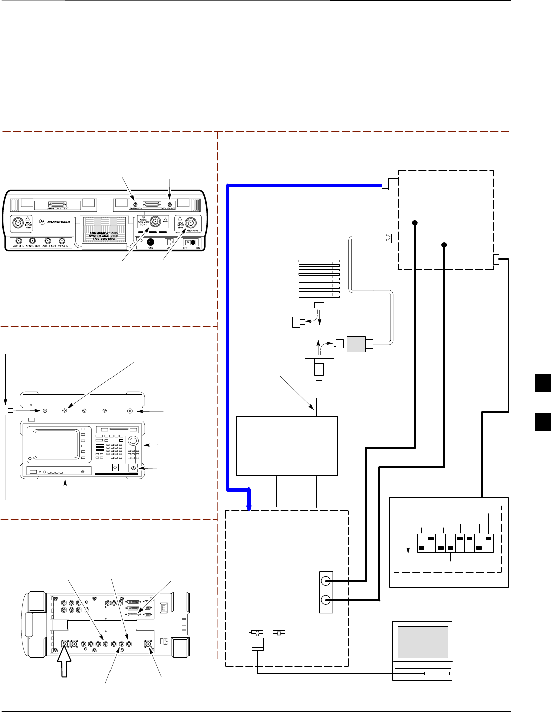
Test Equipment Setup – continued
Jun 2004 1X SC480 BTS Hardware Installation, Optimization/ATP, and FRU 6-63
DRAFT
Set–up for ATP Figure 6-19 and Figure 6-20 show the test set connections for ATP tests.
Figure 6-19: IS–95A/B ATP Test Set–up–
CyberTest, Advantest R3465, and Agilent 8935
Motorola CyberTest
TEST SETS Optimization/ATP SET UP
RF
IN/OUT
SYNC MONITOR
EVEN SEC TICK
PULSE REFERENCE
FROM CSA CARD
FREQ MONITOR
19.6608 MHZ CLOCK
REFERENCE FROM
CSA CARD
Advantest Model R3465
INPUT 50Ω
GPIB CONNECTS
TO BACK OF UNIT
NOTE: The 30 dB directional coupler is not
used with the Cybertest test set. The TX
cable is connected directly to the Cybertest
test set.
RF OUT 50Ω
FREQ MONITOR
19.6608 MHZ CLOCK
REFERENCE FROM
CSA CARD
RF GEN
OUT
SYNC MONITOR EVEN
SEC TICK PULSE
REFERENCE FROM CSA
CARD
BNC
“T”
TO EXT TRIGGER CONNECTOR
ON REAR OF TEST SET
(FOR DETAILS, SEE
FIGURE B-15)
RS232–GPIB
INTERFACE BOX
GPIB
CABLE
RS232 NULL
MODEM
CABLE
S MODE
DATA FORMAT
BAUD RATE
GPIB ADRS G MODE
ON
BTS CDMA
WinLMF
DIP SWITCH SETTINGS
LAN
B
LAN
A
RX TEST
CABLE
GPIB
RF IN/OUT
OR
INPUT 50 Ω
RF GEN OUT,
RF OUT 50Ω,
OR RF IN/OUT
FREQ
MONITOR
SYNC
MONITOR
CSA
50 Ω
TERM
.
TX TEST
CABLE
DIRECTIONAL
COUPLER
(30 DB)
100–WATT (MIN.)
NON–RADIATING
RF LOAD
TX TEST
CABLE
* BLACK RECTANGLES
REPRESENT THE RAISED
PART OF SWITCHES
EXT
REF IN
EVEN
SECOND/
SYNC IN
NOTE: IF BTS IS EQUIPPED
WITH DRDCS (DUPLEXED RX/TX
SIGNALS), BOTH THE TX AND RX
TEST CABLES CONNECT TO THE
DRDC ANTENNA CONNECTOR.
(SEE FIGURE 6-22.)
0–20 DB IN–LINE
ATTENUATOR
IMPORTANT:
WHEN PERFORMING LOW POWER TESTING BYPASS THE COUPLER AND
ATTENUATOR AND CONNECT DIRECTLY TO THE ANALYZER.
Agilent 8935 Series E6380A (formerly HP 8935)
RF IN/OUT
HP–IB
TO GPIB
BOX
SYNC MONITOR
EVEN SEC TICK
PULSE REFERENCE
FROM CSA CARD
FREQ MONITOR
19.6608 MHZ CLOCK
REFERENCE FROM
CSA CARD
10 MHZ
REF OUT
Communications
System Analyzer
ANT
IN
cCLPA
ANTENNA
TX IN
RX OUT
RX MAINRX DIV TX1
HIGH POWER
CONNECTION
6
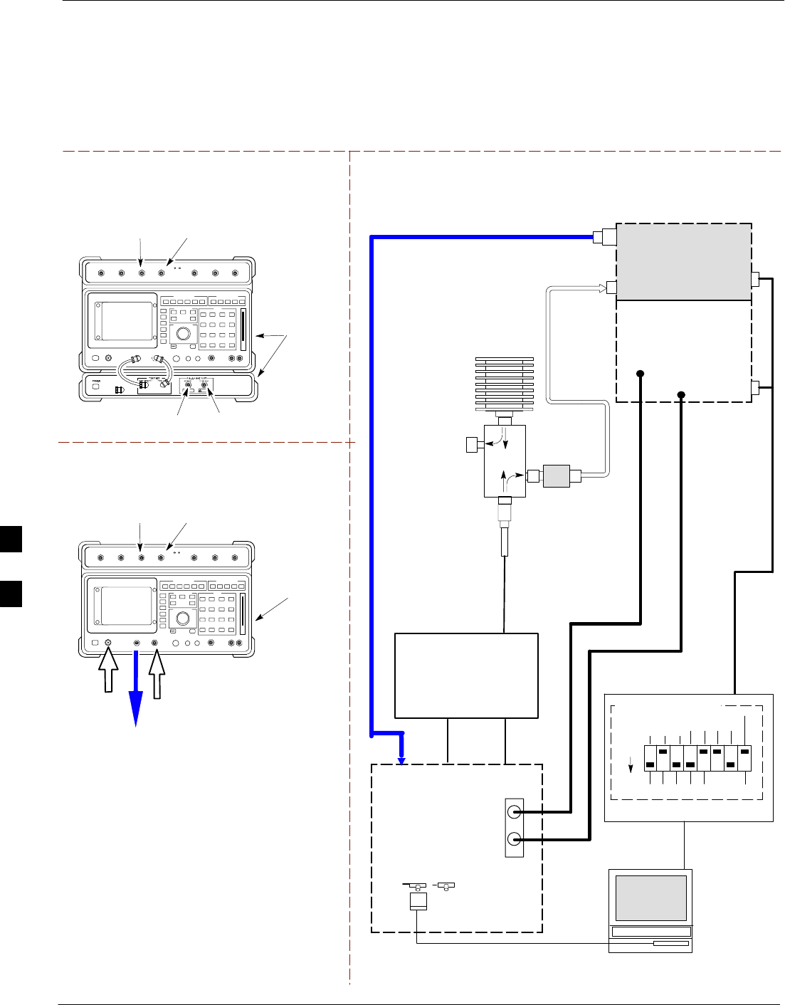
Test Equipment Setup – continued
6-64 1X SC480 BTS Hardware Installation, Optimization/ATP, and FRU Jun 2004
DRAFT
Figure 6-20: IS–95A/B ATP Test Setup – HP 8921A
RF OUT
ONLY
Hewlett Packard Model HP 8921A W/PCS Interface
(for 1900 MHz)
GPIB
CONNECTS
TO BACK OF
UNITS
SYNC MONITOR
EVEN SEC TICK
PULSE REFERENCE
FROM CSA CARD
FREQ MONITOR
19.6608 MHZ CLOCK
REFERENCE FROM
CSA CARD
TEST SETS Optimization/ATP SET UP
RF
IN/OUT
GPIB
CONNECTS
TO BACK OF
UNIT
SYNC MONITOR
EVEN SEC TICK
PULSE REFERENCE
FROM CSA CARD
FREQ MONITOR
19.6608 MHZ CLOCK
REFERENCE FROM
CSA CARD
Hewlett Packard Model HP 8921A
(for 800 MHz)
RF
IN/OUT
DUPLEX
OUT
RS232–GPIB
INTERFACE BOX
GPIB
CABLE
RS232 NULL
MODEM
CABLE
S MODE
DATA FORMAT
BAUD RATE
GPIB ADRS G MODE
ON
BTS CDMA
WinLMF
DIP SWITCH SETTINGS
LAN
B
LAN
A
RX TEST
CABLE
GPIB
PCS INTERFACE
INPUT/OUTPUT
PORTS
FREQ
MONITOR
SYNC
MONITOR
CSA
50 Ω
TERM
.
TX TEST
CABLE
DIRECTIONAL
COUPLER
(30 DB)
100–WATT (MIN.)
NON–RADIATING
RF LOAD
TX TEST
CABLE
* BLACK RECTANGLES
REPRESENT THE RAISED
PART OF SWITCHES
EXT
REF IN EVEN
SECOND/
SYNC IN
HP PCS
INTERFACE*
0–20 DB IN–LINE
ATTENUATOR
* FOR 1900 MHZ
ONLY
RF OUT ONLY
RF IN/OUT
NOTE:
FOR 800 MHZ TESTING, CONNECT CABLES TO THE
HP 8921A AS FOLLOWS:
RX TEST CABLE TO DUPLEX OUT
TX TEST CABLE TO RF IN/OUT
Communications
System Analyzer
ANT
IN
cCLPA
ANTENNA
TX IN
RX OUT
RX MAINRX DIV TX1
Signal
Generator
6
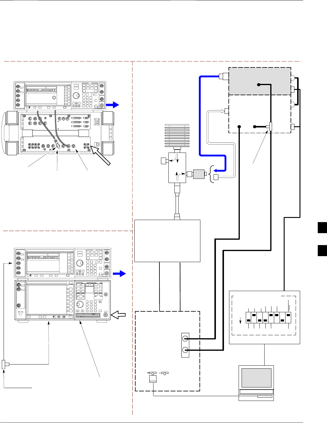
Test Equipment Setup – continued
Jun 2004 1X SC480 BTS Hardware Installation, Optimization/ATP, and FRU 6-65
DRAFT
TEST SETS Optimization/ATP SET UP
Figure 6-21: IS–95A/B and CDMA2000 1X ATP Test Setup Agilent Test Equipment
RF INPUT
50 Ω
RF
OUTPUT
50 Ω
Agilent E4432B (Top) and E4406A (Bottom)
FREQ MONITOR
19.6608 MHZ CLOCK
REFERENCE FROM
CSA CARD
SYNC MONITOR
EVEN SEC TICK
PULSE REFERENCE
FROM CSA CARD
BNC
“T”
TO TRIGGER IN
ON REAR OF
TRANSMITTER
TESTER
TO PATTERN TRIG IN
ON REAR OF SIGNAL
GENERATOR
TO EXT REF IN
ON REAR OF
TRANSMITTER
TESTER
NOTE:
10 MHZ IN ON REAR OF SIGNAL GENERATOR IS CONNECTED TO
10 MHZ OUT (SWITCHED) ON REAR OF TRANSMITTER TESTER
(SEE FIGURE B-18).
RS232–GPIB
INTERFACE BOX
GPIB
CABLE
RS232 NULL
MODEM
CABLE
S MODE
DATA FORMAT
BAUD RATE
GPIB ADRS G MODE
ON
BTS
CDMA
LMF
DIP SWITCH SETTINGS *
LAN
B
LAN
A
Communications
System Analyzer
HP–IB
OR
GPIB
FREQ
MONITOR
SYNC
MONITOR
CSM
BTS
CPLD
ANTENNA
Signal
Generator
GPIB
10 MHZ
IN
10 MHZ
REF OUT
OR
10 MHZ
OUT
TRIGGER IN
OR
EVEN SEC
SYNCH IN
EXT
REF
IN
BNC
“T”
PATTERN
TRIG IN
* BLACK RECTANGLES
REPRESENT THE RAISED
PART OF SWITCHES
RX TEST
CABLE
50 Ω
TERM
.
TX TEST
CABLE
DIRECTIONAL
COUPLER
(30 DB)
100–WATT (MIN.)
NON–RADIATING
RF LOAD
TX TEST
CABLE
2O DB IN–LINE
ATTENUATOR
RF IN/OUT
OR
RF INPUT
50 Ω
RF OUTPUT 50 Ω
Agilent E4432B (Top) and 8935 Series E6380A
(Bottom)
SYNC MONITOR
EVEN SEC TICK
PULSE REFERENCE
FROM CSA CARD
FREQ MONITOR
19.6608 MHZ CLOCK
REFERENCE FROM
CSA CARD
RF
OUTPUT
50 Ω
NOTES:
10 MHZ IN ON REAR OF SIGNAL GENERATOR IS CONNECTED TO
10 MHZ REF OUT ON SIDE OF CDMA BASE STATION TEST SET
PATTERN TRIG IN ON REAR OF SIGNAL GENERATOR IS
CONNECTED TO EVEN SECOND SYNC IN ON SIDE OF CDMA BASE
STATION TEST SET.
(SEE FIGURE B-17)
RF IN/OUT
BNC
“T”
RX OUT TX IN
cCLPA
RX MAIN TX1
6
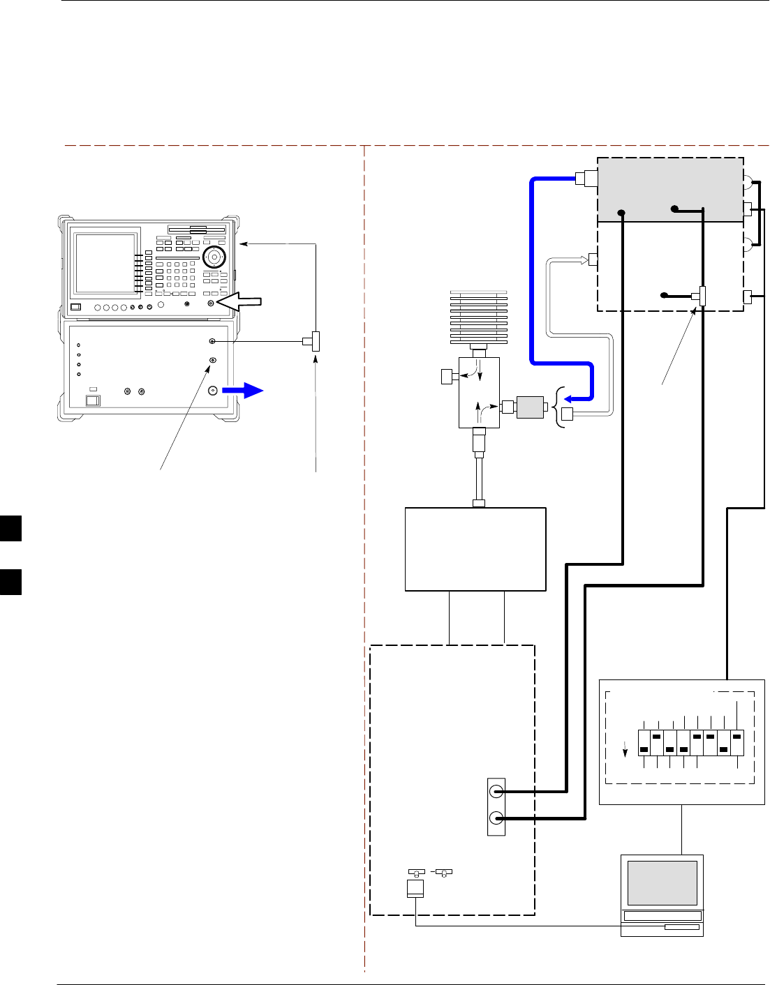
Test Equipment Setup – continued
6-66 1X SC480 BTS Hardware Installation, Optimization/ATP, and FRU Jun 2004
DRAFT
Figure 6-22: IS–95A/B and CDMA2000 1X Optimization/ATP Test Setup – Agilent E4432B/8935 Series
E6380A and E4432B/E4406A Test Equipment
TEST SETS Optimization/ATP SET UP
INPUT 50 Ω
RF OUT
50 Ω
Advantest R3267 (Top) and R3562 (Bottom)
FREQ MONITOR
19.6608 MHZ CLOCK
REFERENCE FROM
CSA CARD
SYNC MONITOR
EVEN SEC TICK
PULSE REFERENCE
FROM CSA CARD
BNC
“T”
NOTE:
SYNTHE REF IN ON REAR OF SIGNAL GENERATOR IS
CONNECTED TO 10 MHZ REF OUT ON REAR OF
SPECTRUM ANALYZER (SEE FIGURE B-19)
TO EXT TRIG
ON REAR OF
SPECTRUM
ANALYZER
RS232–GPIB
INTERFACE BOX
GPIB
CABLE
RS232 NULL
MODEM
CABLE
S MODE
DATA FORMAT
BAUD RATE
GPIB ADRS G MODE
ON
BTS
CDMA
WinLMF
DIP SWITCH SETTINGS
LAN
B
LAN
A
INPUT
50 Ω
RF OUT
50 Ω
FREQ
MONITOR
SYNC
MONITOR
CSA
BNC
“T”
GPIB
GPIB
SYNTHE
REF
IN
10 MHZ
OUT
EXT
TRIG IN
MOD TIME
BASE IN
EXT TRIG
* BLACK RECTANGLES
REPRESENT THE RAISED
PART OF SWITCHES
RX TEST
CABLE
50 Ω
TERM
.
TX TEST
CABLE
DIRECTIONAL
COUPLER
(30 DB)
100–WATT (MIN.)
NON–RADIATING
RF LOAD
TX TEST
CABLE
0–20 DB IN–LINE
ATTENUATOR
Spectrum
Analyzer
Signal
Generator
cCLPA
ANTENNA
TX IN
RX OUT
TX 1
RX MAIN
6
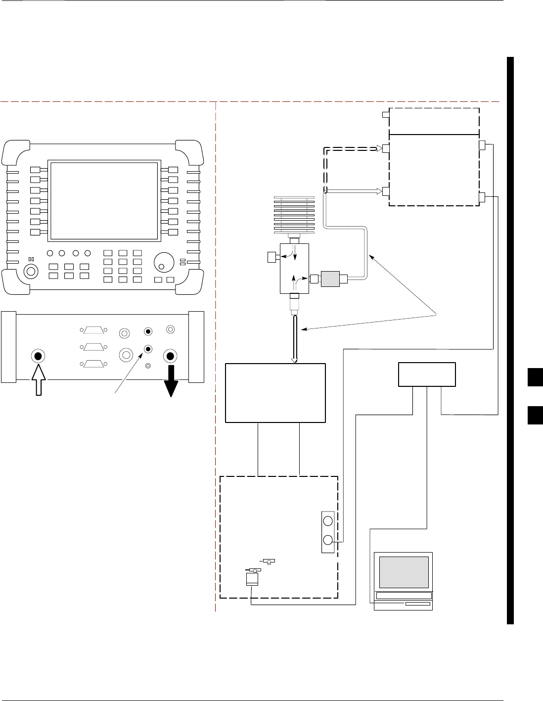
Test Equipment Setup – continued
Jun 2004 1X SC480 BTS Hardware Installation, Optimization/ATP, and FRU 6-67
DRAFT
TEST SET ATP TEST SET UP
UNIVERSAL TWISTED PAIR (UTP)
CABLE (RJ45 CONNECTORS)
CDMA
WinLMF
INTERNAL
ETHERNET
CARD
RF INPUT 50 Ω
OR INPUT 50 Ω
50 Ω
TERM
DIRECTIONAL
COUPLER
(30 DB)
100–WATT (MIN.)
NON–RADIATING
RF LOAD TX TEST
2O DB IN–LINE
ATTENUATOR
ETHERNET HUB
RX TEST
RX MAIN TX 1
TEST
CABLES
NOTE: USE THE SAME
CABLE SET FOR TX AND RX
ATP. SWITCH THE CABLES
DURING ALL ATP TESTS AS
SHOWN.
POWER METER
PORT 2
RF IN
PORT 1
RF OUT
Agilent E7495A
PORT 1
RF OUT
PORT 2
RF IN
SYNC MONITOR
EVEN SEC TICK
PULSE REFERENCE
FROM CSM BOARD
Use only
Agilent supplied
power adapter
GPS
GPIO
Serial 1
Serial 2
Power REF
50 MHz
Sensor
Ext Ref
In
Even Second
Sync In
Antenna
Port 1
RF Out / SWR
Port 2
RF In
EVEN SECOND
SYNC IN
BTS
10BASET/
10BASE2
CONVERTER
LAN
B
LAN
A
SYNC
MONITOR
CSA
FREQ
MONITOR
Figure 6-23: IS–95A/B and CDMA2000 1X Optimization/ATP Test Setup – Agilent E7495A
cCLPA
TX IN
RX OUT
ANTENNA
Communications
System Analyzer
6
Test Set Calibration
6-68 1X SC480 BTS Hardware Installation, Optimization/ATP, and FRU Jun 2004
DRAFT
Background
Proper test equipment calibration helps to ensure accurate BTS
optimization and acceptance testing by assuring that the test equipment
and associated cables do not introduce measurement errors.
If the test equipment set being used to optimize or test the
BTS has been calibrated and maintained as a set, this
procedure does not need to be performed.
NOTE
This procedure must be performed prior to beginning the optimization.
Verify all test equipment (including all associated cables and adapters
actually used to interconnect test equipment items and the BTS) has been
calibrated and maintained as a set.
If any piece of test equipment, test cable, or RF adapter
that makes up the calibrated test equipment set has been
replaced, the set must be re-calibrated. Failure to do so can
introduce measurement errors, resulting in incorrect
measurements and degradation to system performance.
Motorola recommends repeating cable calibration before
testing at each BTS site.
CAUTION
Calibration of the communications system analyzer (or
equivalent test equipment) must be performed at the site
before calibrating the overall test equipment set. Calibrate
the test equipment after it has been allowed to warm–up
and stabilize for a a minimum of 60 minutes.
NOTE
Calibration Procedures
Included
Automatic
Procedures included in this section use the WinLMF automated
calibration routine to determine path losses of the supported
communications analyzer, power meter, associated test cables, adapters,
and (if used) antenna switch that make up the overall calibrated test
equipment set. After calibration, the gain/loss offset values are stored in
a test measurement offset file on the WinLMF computer.
6

Test Set Calibration – continued
Jun 2004 1X SC480 BTS Hardware Installation, Optimization/ATP, and FRU 6-69
DRAFT
Manual
Agilent E4406A Transmitter Tester – The E4406A does not support
the power level zeroing calibration performed by the WinLMF. If this
instrument is to be used for Bay Level Offset calibration and calibration
is attempted with the WinLMF Calibrate Test Equipment function, the
WinLMF will return a status window failure message stating that zeroing
power is not supported by the E4406A. Refer to the Equipment
Calibration section of Appendix B for instructions on using the
instrument’s self–alignment (calibration) function prior to performing
Bay Level Offset calibration.
Power Meters – Manual power meter calibration procedures to be
performed prior to automated calibration are included in the Equipment
Calibration section of Appendix B .
Cable Calibration – Manual cable calibration procedures using the HP
8921A and Advantest R3465 communications system analyzers are
provided in the Manual Cable Calibration section of Appendix B, if
needed.
GPIB Addresses
GPIB addresses can range from 1 through 30. The WinLMF will accept
any address in that range, but the numbers entered in the WinLMF
Options window GPIB address boxes (Table 6-23 and Table 6-24) must
match the addresses set in the test equipment. Motorola recommends
using 1 for a CDMA signal generator, 13 for a power meter, and 18 for a
communications system analyzer. To verify and, if necessary, change the
GPIB addresses of the test equipment, refer to the Setting GPIB
Addresses section of Appendix B.
Selecting Test Equipment
Serial Connection and Network Connection tabs are provided in the
WinLMF Options window to specify the test equipment connection
method. The Serial Connection tab is used when the test equipment
items are connected directly to the WinLMF computer through a GPIB
box (normal setup). The Network Connection tab is used when the test
equipment is to be connected remotely via a network connection or the
Agilent E7495A Communications Test Set is used.
Prerequisites
Be sure the following have been completed before selecting test
equipment:
STest equipment is correctly connected and turned on.
SGPIB addresses set in the test equipment have been verified as correct
using the applicable procedures in Appendix B.
SWinLMF computer serial port and test equipment are connected to the
GPIB box.
6

Test Set Calibration – continued
6-70 1X SC480 BTS Hardware Installation, Optimization/ATP, and FRU Jun 2004
DRAFT
Selecting Test Equipment
Test equipment may be selected either manually with operator input or
automatically using the WinLMF autodetect feature.
Manually Selecting Test
Equipment in a Serial
Connection Tab
Test equipment can be manually specified before or after the test
equipment is connected. The WinLMF does not attempt to verify the test
equipment is actually detected when manual selection is specified.
Follow the procedure in Table 6-23 to manually select test equipment.
Table 6-23: Procedure for Selecting Test Equipment Manually in the Serial Connection Tab
Step Action
1In the WinLMF window menu bar, click Tools and select Options... from the pull–down menu.
The WinLMF Options window appears.
2If it is not in the forefront, click on the Serial Connection tab.
3Select the correct serial port in the COMM Port: pick list (normally COM1).
4If it is not selected (black dot showing), click on the Manual Specification button.
5Click on the check box(es) corresponding to the test equipment item(s) to be used.
6Type the GPIB address in the corresponding GPIB address box (refer to the Setting GPIB Addresses
section of Appendix B for directions on verifying and/or changing test equipment GPIB addresses).
Motorola–recommended addresses are:
1 = signal generator
13 = power meter
18 = communications system analyzer
* IMPORTANT
When test equipment items are manually selected by the operator, the WinLMF defaults to using a
power meter for RF power measurements. The WinLMF will use a communications system analyzer
for RF power measurements only if a power meter is not selected (power meter checkbox not
checked).
7Click on Apply. (The button will darken until the selection has been committed.)
NOTE
With manual selection, the WinLMF does not attempt to detect the test equipment to verify it is
connected and communicating with the WinLMF.
To verify and, if necessary, change the GPIB address of the test equipment, refer to Appendix B.
8Click on Dismiss to close the WinLMF Options window.
6

Test Set Calibration – continued
Jun 2004 1X SC480 BTS Hardware Installation, Optimization/ATP, and FRU 6-71
DRAFT
Automatically Selecting Test
Equipment in the Serial
Connection Tab When using the auto-detection feature to select test equipment, the
WinLMF determines which test equipment items are actually
communicating with WinLMF. Follow the procedure in Table 6-24 to
use the auto-detection feature.
Table 6-24: Procedure for Selecting Test Equipment Using Auto-Detect
Step Action
1In the WinLMF window menu bar, click Tools and select Options... from the pull–down menu. The
WinLMF Options window appears.
2If it is not in the forefront, click on the Serial Connection tab.
3Select the correct serial port in the COMM Port: pick list (normally COM1).
4If it is not selected (no black dot showing), click on the Auto–Detection button.
5If they are not already displayed in the box labeled GPIB address to search, click in the box and type
in the GPIB addresses for the test equipment to be used, separating each address with commas and no
spaces. (Refer to the Setting GPIB Addresses section of Appendix B for instructions on verifying
and/or changing test equipment GPIB addresses.)
NOTE
During the GPIB address search for a test equipment item to perform RF power measurements (that is,
for TX calibration), the WinLMF will select the first item it finds with the capability to perform the
measurement. If, for example, the address sequence 13,18,1 is included in the GPIB addresses to
search box, the power meter (GPIB address 13) will be used for RF power measurements. If the
address sequence 18,13,1 is included, the WinLMF will use the communications system analyzer
(GPIB address 18) for power measurements.
6 Click Apply. The button will darken until the selection has been committed. A check mark will appear
in the applicable Manual Configuration section check boxes for detected test equipment items.
7 Click Dismiss to close the WinLMF Options window.
Calibrating Test Equipment
The WinLMF Calibrate Test Equipment function zeros the power
measurement level of the test equipment item that is to be used for TX
calibration and audit. If both a power meter and an analyzer are
connected (for example, an HP 437 and an HP8921A/600), only the
power meter is zeroed.
The Agilent E4406A transmitter tester does not support
power measurement level zeroing. Refer to the Equipment
Calibration section of Appendix B for E4406A calibration.
NOTE
6

Test Set Calibration – continued
6-72 1X SC480 BTS Hardware Installation, Optimization/ATP, and FRU Jun 2004
DRAFT
Prerequisites
SWinLMF computer serial port and test equipment are connected to the
GPIB box.
STest equipment is turned on and has warmed up for at least 60
minutes.
STest equipment has been selected in the WinLMF (Table 6-23 or
Table 6-24)
Follow the procedure in Table 6-25 to calibrate the test equipment.
Table 6-25: Procedure for Test Equipment Calibration
Step Action
1From the Util menu, select Calibrate Test Equipment from the pull–down menu. A Directions
window is displayed.
2Follow the directions provided.
3Click on Continue to close the Directions window and start the calibration process. A status report
window is displayed.
4Click on OK to close the status report window.
Calibrating Cables Overview
The WinLMF Cable Calibration function is used to measure the path
loss (in dB) for the TX and RX cables, adapters, directional couplers,
and attenuators that make up the cable configurations used for testing. A
communications system analyzer is used to measure the loss of both the
TX test cable and the RX test cable configurations. WinLMF cable
calibration consists of the following processes:
1. Measure the loss of a short cable. This is done to compensate for any
measurement error of the communications system analyzer. The
short cable, which is used only for the calibration process, is
connected in series with both the TX and RX test cable
configurations when they are measured. The measured loss of the
short cable is deducted from the measured loss of the TX and RX
test cable configurations to determine the actual loss of the
configurations. This deduction is done so any error in the analyzer
measurement will be adjusted out of both the TX and RX
measurements.
2. Measure the loss of the short cable plus the RX test cable
configuration. The RX test cable configuration normally consists
only of a coax cable with type–N connectors that is long enough to
reach from the BTS RX connector to the test equipment. When the
BTS antenna connectors carry duplexed TX and RX signals, a
directional coupler and, if required by BTS type, an additional
attenuator are also required for the RX test cable configuration.
These additional items must be included in the path loss
measurement.
6

Test Set Calibration – continued
Jun 2004 1X SC480 BTS Hardware Installation, Optimization/ATP, and FRU 6-73
DRAFT
3. Measure the loss of the short cable plus the TX test cable
configuration. The TX test cable configuration normally consists of
two coax cables with type–N connectors, a directional coupler, a
termination load with sufficient rating to dissipate the BTS output
power, and an additional attenuator, if required by the BTS type. The
total path loss of the TX test configuration must be as required for
the BTS (normally 30 or 50 dB). The Motorola Cybertest analyzer is
different from other communications system analyzers because the
required attenuation/load is built into the test set. Because of this,
the Cybertest TX test configuration consists only of the required
length coax cable.
Calibrating Test Cable
Configurations with a
Communications System
Analyzer
Cable Calibration is used to calibrate both TX and RX test cables.
WinLMF cable calibration cannot be accomplished with an
HP8921A analyzer for 1.9 GHz. A different analyzer type
or the signal generator and spectrum analyzer method
(Table 6-27 and Table 6-28) must be used. Cable
calibration values must be manually entered into the
WinLMF cable loss file if the signal generator and
spectrum analyzer method is used. To use the HP8921A for
manual test cable configuration calibration for 800 MHz
BTSs, refer to the Manual Cable Calibration section of
Appendix B.
NOTE
Prerequisites
STest equipment is turned on and has warmed up for at least 60
minutes. Agilent E7495A requires only 30 minute warmup.
STest equipment has been selected in the WinLMF (Table 6-23 or
Table 6-24).
STest equipment has been calibrated and correctly connected for the
type of test cable configuration to be calibrated.
Calibrating cables
Refer to Figure 6-21 or Figure 6-22 and follow the procedure in
Table 6-26 to calibrate the test cable configurations.
Table 6-26: Procedure to Test Cabling Calibration using Communication System Analyzer
nStep Action
1 Click Util in the BTS menu bar, and select Cable Calibration... in the pull–down menu. A Cable
Calibration window is displayed.
. . . continued on next page
6

Test Set Calibration – continued
6-74 1X SC480 BTS Hardware Installation, Optimization/ATP, and FRU Jun 2004
DRAFT
Table 6-26: Procedure to Test Cabling Calibration using Communication System Analyzer
nActionStep
2Enter one or more channel numbers in the Channels box.
NOTE
Multiple channel numbers must be separated by a comma with no spaces (for example: 200,800).
When two or more channel numbers are entered, the cables will be calibrated for each channel.
Interpolation will be accomplished for other channels, as required, for TX calibration.
3 Select TX and RX CABLE CAL, TX CABLE CAL or RX CABLE CAL in the Cable
Calibration picklist.
4 Click OK, and follow the directions displayed for each step. A status report window will be
displayed with the results of the cable calibration.
Calibrate Test Cabling Using
Signal Generator & Spectrum
Analyzer
Refer to Figure 6-24 and follow the procedure in Table 6-27 to calibrate
the TX test cable configuration for all BTSs or the RX ATP test cable
configuration for BTSs with duplexed TX/RX using the signal generator
and spectrum analyzer. Refer to Figure 6-25 and follow the procedure in
Table 6-28 to calibrate the test cable configuration for non–duplexed RX
using the signal generator and spectrum analyzer.
Table 6-27: Procedure to Calibrate TX/Duplexed RX Test Cabling Using
Signal Generator & Spectrum Analyzer
Step Action
1Connect a short test cable between the spectrum analyzer and the signal generator as shown in
Figure 6-24, detail “A” (top portion of figure).
2Set signal generator to 0 dBm at the customer frequency of:
869–894 MHz or 1930–1990 MHz
3Use spectrum analyzer to measure signal generator output (see Figure 6-24, A) and record the value.
4Connect the spectrum analyzer’s short cable to point B, (as shown in the lower right portion of the
diagram) to measure cable output at customer frequency of:
869–894 MHz or 1930–1990 MHz
Record the value at point B.
5Calibration factor = (value measured with detail “A” setup) – (value measured with detail “B” setup)
Example: Cal factor = –1 dBm – (–53.5 dBm) = 52.5 dB
NOTE
The short cable is used for calibration only. It is not part of the final test setup. After calibration is
completed, do not re-arrange any cables. Use the test cable configuration as is to ensure test
procedures use the correct calibration factor.
6
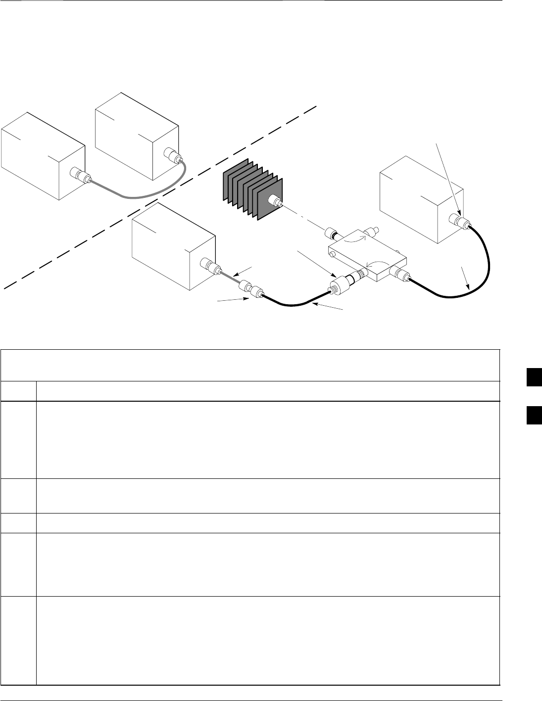
Test Set Calibration – continued
Jun 2004 1X SC480 BTS Hardware Installation, Optimization/ATP, and FRU 6-75
DRAFT
Figure 6-24: Cal Setup for TX/Duplexed RX Test Cabling
Using Signal Generator & Spectrum Analyzer
50 OHM
TERMINATION
30 DB
DIRECTIONAL
COUPLER
Spectrum
Analyzer
Signal
Generator
A
Spectrum
Analyzer
40W NON–RADIATING
RF LOAD
B
SHORT TEST CABLE
Signal
Generator
THIS WILL CONNECT TO THE POWER METER OR COMMUNICATIONS
SYSTEM ANALYZER DURING TX CALIBRATION AND TO THE
COMMUNICATIONS SYSTEM ANALYZER DURING TX AND RX ATP TESTS.
SHORT
TEST
CABLE
20DB 20 W IN–LINE
ATTENUATOR FOR
1.9 GHZ
THIS WILL CONNECT TO THE BTS TX
ANTENNA CONNECTOR DURING TX
CALIBRATION AND TO THE TX/RX ANTENNA
CONNECTORS DURING ATP TESTS.
TX TEST
CABLE
RX TEST CABLE FOR RX ATP TEST
OR
SECOND TX TEST CABLE FOR TX CAL AND ATP
Table 6-28: Procedure for Calibrating Non–Duplexed RX Test Cabling Using
Signal Generator & Spectrum Analyzer
Step Action
NOTE
When preparing to calibrate a BTS with Duplexed TX and RX the RX cable calibration must be done
using calibration setup in Figure 6-24 and the procedure in Table 6-27.
1Connect a short test cable between the spectrum analyzer and the signal generator as shown in
Figure 6-25, detail “A” (top portion of figure).
2Set signal generator to –10 dBm at the customer’s RX frequency of:
824–849 for North American Cellular or 1850–1910 MHz band for North American PCS
3Use spectrum analyzer to measure signal generator output (see Figure 6-25, A) and record the value.
4Connect the test setup, as shown in the lower portion of the diagram (see Figure 6-25, B) to measure
the output at the customer’s RX frequency of:
824–849 for North American Cellular or 1850–1910 MHz band for North American PCS
Record the value at point B.
5Calibration factor = (value measured with detail “A” setup) – (value measured with detail “B” setup)
Example: Cal factor = –12 dBm – (–14 dBm) = 2 dB
NOTE
The short test cable is used for test equipment setup calibration only. It is not part of the final test
setup. After calibration is completed, do not re-arrange any cables. Use the test cable configuration
as–is to ensure test procedures use the correct calibration factor.
6
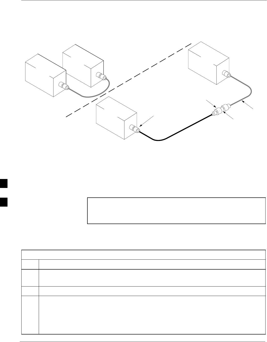
Test Set Calibration – continued
6-76 1X SC480 BTS Hardware Installation, Optimization/ATP, and FRU Jun 2004
DRAFT
Figure 6-25: Cal Setup for Non–Duplexed RX Test Cabling Using Signal Generator & Spectrum Analyzer
Spectrum
Analyzer
Signal
Generator
A
B
Spectrum
Analyzer
SHORT
TEST
CABLE
CONNECTION TO THE COMMUNICATIONS
SYSTEM ANALYZER RF OUTPUT
CONNECTOR DURING RX MEASUREMENTS
Signal
Generator
BULLET
CONNECTOR
TX test
cable
SHORT TEST
CABLE
CONNECTION TO THE BTS RX ANTENNA
CONNECTOR DURING RX ATP
IMPORTANT: IF BTS TX/RX SIGNALS ARE
DUPLEXED, THE RX TEST CABLE CONNECTS
TO THE DUPLEXED ANTENNA CONNECTOR
AND MUST USE/BE CALIBRATED WITH THE 30
DB DIRECTIONAL COUPLER AND 20 DB
IN–LINE ATTENUATOR. SEE FIGURE 6-24.
Setting Cable Loss Values Cable loss values for TX and RX test cable configurations are normally
set by accomplishing automatic cable calibration using the WinLMF and
the applicable test equipment. The WinLMF stores the measured loss
values in the cable loss files. The cable loss values can also be set or
changed manually. Follow the procedure in Table 6-29 to set cable loss
values.
CAUTION If cable calibration was performed without using the WinLMF,
cable loss values must be manually entered in the WinLMF
database. Failure to do this will result in inaccurate BTS
calibration and reduced site performance.
Prerequisites
SWinLMF is logged into the BTS
Table 6-29: Procedure for Setting Cable Loss Values
Step Action
1 Click Util in the BTS menu bar, and select Edit > Cable Loss in the pull–down menus.
–A tabbed data entry pop–up window will appear.
2Click on the TX Cable Loss tab or the RX Cable Loss tab, as required.
3To add a new channel number, perform the following:
3a – Click on the Add Row button.
3b – Click in the Channel # or Loss (dBm) column, as required.
3c – Enter the desired value.
. . . continued on next page
6

Test Set Calibration – continued
Jun 2004 1X SC480 BTS Hardware Installation, Optimization/ATP, and FRU 6-77
DRAFT
Table 6-29: Procedure for Setting Cable Loss Values
Step Action
4To edit existing values, click in the data box to be changed and change the value.
5To delete a row, click on the row and then click on the Delete Row button.
6For each tab with changes, click on the Save button to save displayed values.
7Click on the Dismiss button to close the window.
NOTE
SValues entered or changed after the Save button was used will be lost when the window is
dismissed.
SIf cable loss values exist for two different channels the WinLMF will interpolate for all other
channels.
SEntered values will be used by the WinLMF as soon as they are saved. It is not necessary to log out
and log back into the WinLMF for changes to take effect.
Setting TX and RX Directional
Coupler Loss Value
If an in–service TX or RX directional coupler is installed in the RF path,
the loss due to the added coupler (e.g., 30 dB) must be manually entered
so it will be included in the WinLMF TX calibration and audit
calculations and the RX FER test. Follow the procedure in Table 6-30 to
enter directional coupler loss values.
Prerequisites
SWinLMF is logged into the BTS
SPath loss, in dB, of the TX coupler must be known.
Table 6-30: Procedure for Setting TX and RX Directional Coupler Loss Values
Step Action
1 Click Util in the BTS menu bar, and select Edit > Coupler Loss... in the pull–down menus.
–A tabbed data entry pop–up window will appear.
2Click on the TX Coupler Loss tab or the RX Coupler Loss tab, as required
3Click in the Loss (dBm) column for each carrier that has a coupler and enter the appropriate value.
4To edit existing values, click in the data box to be changed and change the value.
5For each tab with changes, click on the Save button to save displayed values.
. . . continued on next page
6

Test Set Calibration – continued
6-78 1X SC480 BTS Hardware Installation, Optimization/ATP, and FRU Jun 2004
DRAFT
Table 6-30: Procedure for Setting TX and RX Directional Coupler Loss Values
Step Action
6Click on the Dismiss button to close the window.
NOTE
SValues entered or changed after the Save button is used will be lost when the window is dismissed.
SThe In–Service Calibration check box in the Tools > Options > BTS Options tab must be
checked before entered TX coupler loss values will be used by the TX calibration and audit
functions.
SNew or changed values will be used by the LMF as soon as they are saved. Logging out and logging
in again are not required to cause saved changes to take effect.
6

Bay Level Offset Calibration
Jun 2004 1X SC480 BTS Hardware Installation, Optimization/ATP, and FRU 6-79
DRAFT
Purpose of Bay Level Offset
Calibration
Bay Level Offset (BLO) calibration is the central activity of the
optimization process. BLO calibration compensates for normal
equipment variations within the BTS RF paths and assures the correct
transmit power is available at the BTS antenna connectors to meet site
performance requirements.
What is BLO Calibration?
Description
BLO calibration is the complete title of what is normally referred to as
“calibration.” Calibration identifies the accumulated gain in every
transmit path at the BTS site. The transmit path BLO values determined
during calibration are stored in the LMF calibration data file, and are
subsequently downloaded to each BBX. When transmit path calibration
is performed, receive path BLO values will automatically be set to the
default value in the LMF calibration file and downloaded.
Component Verification During
Calibration
TX Path Calibration
TX path calibration supports verification of correct BTS installation, RF
cabling installation and performance, functionality of all equipment
installed in the transmit RF chain, and the proper functioning of each
transmit RF path. External test equipment is used to calibrate and audit
the TX paths of the BTS.
RX Path Calibration
RX path calibration is not required or supported on CDMA BTS
systems. Default RX calibration values are written to the RX calibration
data files during the TX calibration process. RX functionality is verified
during Frame Erasure Rate (FER) testing.
When to Calibrate BLOs Calibration to determine BLO:
1. Is required after initial BTS installation.
2. Must be done once each year for an operational BTS site.
3. Is recommended by Motorola for all associated RF paths after
replacing any of the following components:
– BBX card
– CCP2 shelf
– cCLPA
6

Bay Level Offset Calibration – continued
6-80 1X SC480 BTS Hardware Installation, Optimization/ATP, and FRU Jun 2004
DRAFT
BLO Calibration Data File
During the calibration process, the LMF creates a calibration (CAL) data
file where BLO values are stored. After calibration has been completed,
these offset values must be downloaded to the BBXs using the LMF
BLO download function. A detailed description of the file organization
and content is provided in the following paragraphs
NOTE Due to the size of the file, Motorola recommends printing out a
copy of a bts–#.cal file and referring to it for the following
descriptions.
SWhen referring to the CAL file print–out it can be seen that there is
one BBX slot with 20 “calibration entries” per BBX (sector) for each
branch. Two calibration entries define a single “calibration point;”
therefore there are ten calibration points in each branch for each BBX.
– The first entry for a calibration point (all odd entries) identifies the
CDMA channel (frequency) where the BLO is measured. The
second calibration entry (all even entries) is the power set level
(PwrLvlAdj) for that frequency. The valid range for PwrLvlAdj is
from 2500 to 27500 (2500 corresponds to –125 dBm and 27500
corresponds to +125 dBm).
– The ten calibration points for each slot–branch combination must be
stored in order of increasing frequency. If less than ten points
(frequencies) are calibrated, the BLO data for the highest frequency
calibrated is written into the remainder of the ten points for that
slot–branch.
Example:
C[1]=384 (odd cal entry)
C[2]=19102 (even cal entry)
C[3]=777 (odd cal entry)
C[4]=19086 (even cal entry)
C[19]=777 (odd cal entry)
C[20]=19086 (even cal entry)
.
.
.
= 1 “calibration point”
= 1 “calibration point”
= 1 “calibration point”
In the example above, BLO was measured at only two frequencies
(channels 384 and 777) for CCP2 slot BBX–1 transmit. The BLO data
for the highest frequency measured (channel 777) will be written to
the remaining eight transmit calibration points (defined by entries
C[5] through C[20]) for BBX–1.
Slot Block Temperature Compensation – Each BBX slot Block also
has a temperature compensation data section (TempLevelCal) where
power level compensation factors for temperature variations are stored.
6

Bay Level Offset Calibration – continued
Jun 2004 1X SC480 BTS Hardware Installation, Optimization/ATP, and FRU 6-81
DRAFT
CAL File and BLO Data Download
When BLO data is downloaded to the BBXs after calibration, the data is
downloaded to the devices in the order it is stored in the CAL file. TX
calibration data (entries C[1] – C[60]) are sent first. Data for the ten
BBX slot 1 calibration points (entries C[1] – C[20]) are sent initially,
followed by data for the ten BBX slot 2 calibration points (entries C[21]
– C[40]), and so on. The RX calibration data is sent next in BBX slot
sequence, followed by RX Diversity calibration data.
BLO for Expansion BTS
The BLO Ranges for expansion BTS configurations are listed below:
Low Power
S1.9 GHz: 1 to 4 carriers: –15 7 dB
S1.9 GHz: 5 to 8 carriers: –19 7dB
High Power (1 or 2 cCLPAs)
S1.9 GHz: 1 to 2 carriers: 46 7 dB
S1.9 GHz: 3 to 4 carriers: 42 7 dB
S1.9 GHz: 5 to 8 carriers: 40 7dB
Test Equipment Setup for
RF Path Calibration
Follow the procedure in Table 6-31 and refer as needed to Figure 6-15 or
Figure 6-17 to set up test equipment.
Table 6-31: Procedure to Set Up Test Equipment for RF Path Calibration
Step Action
1If it has not already been done, refer to the procedure in Table 6-6 (on page 6-17) to interface the LMF
computer terminal to the frame LAN A connector.
2If it has not already been done, refer to Table 6-7 (on page 6-25) to start a GUI LMF session.
3If not already done, select test equipment per the procedure in Table 6-23 or Table 6-24.
4If required, calibrate the test equipment per the procedure in Table 6-25.
! CAUTION
To prevent damage to the test equipment in high power configurations, all transmit (TX) test
connections must be via the 30 dB directional coupler for 1.9 GHz.
Attenuators are not required for low power configuration.
5For TX path calibration, connect the test equipment as shown in Figure 6-15, Figure 6-17, or
Figure 6-18, depending on the communications analyzer being used.
6

Bay Level Offset Calibration – continued
6-82 1X SC480 BTS Hardware Installation, Optimization/ATP, and FRU Jun 2004
DRAFT
Transmit (TX) Path Calibration
Description
The assigned channel frequency and desired power level at the frame TX
ports for transmit calibration are derived from the BTS CDF file. Each
BBX at the site is assigned to a carrier. These are specified respectively
in the carrier field of the ParentCARRIER parameter in each BBXs CDF
file block. The channel frequency for the assigned sector is specified in
the ChannelList parameter of the CDF block for the CARRIER to
which the BBX is assigned.
For Low Power optimization of the SC480, the following adjustments
must be made to the CDF.
SIn the Carrier section of the CDF, verify that the SifPilotPwr is set to
–200.
SIn the BTS section of the CDF, verify that the CageConf is set to 5
(CCP2), and that BIOType is set to 3.
Be sure the bts–#.cdf and cbsc–#.cdf files loaded on the
LMF computer are current. The LMF will obtain carrier
and channel information from these files and insert it into
the appropriate CDMA Test Parameter screen. Failure to
have the most current files from the CBSC can result in
incorrect channel information being used to calibrate the
BTS and unfavorable affects on BTS performance. Carrier
and channel numbers should only be entered manually for
special test cases or as a last resort.
NOTE
The calibration process attempts to adjust the measured power to within
+0.5 dB of the desired power. The calibration will pass if the error is less
than +1.5 dB.
Table 6-32 lists the maximum and minimum power with and without the
cCLPA. The numbers presented may change at a later date.
Table 6-32: Maximum and Minimum Power
TX Configuration Max Power Min Power
Indoor / Low Power –6.0 dBm –16.0 dBm
Outdoor / Low Power –6.0 dBm –16.0 dBm
Indoor / High Power 43.0 dBm / 41.76 dBm* 33.0 dBm
Outdoor / High Power 43.0 dBm / 41.76 dBm* 33.0 dBm
* Non–domestic maximum high power is 41.76 due to TX GSM Elimination filter.
6

Bay Level Offset Calibration – continued
Jun 2004 1X SC480 BTS Hardware Installation, Optimization/ATP, and FRU 6-83
DRAFT
TX Calibration and the LMF
The LMF Tests > TX > TX Calibration... and Tests > All Cal/Audit...
selections perform TX BLO calibration testing for installed BBX(s). The
All Cal/Audit... selection initiates a series of actions to perform TX
calibration, and if calibration is successful, download BLO and perform
TX audit. The TX Calibration... selection performs only TX
calibration. When TX Calibration... is used, BLO download and TX
audit must be performed as separate activities. The CDMA Test
Parameters window which opens when TX Calibration... or All
Cal/Audit... is selected contains several user–selectable features which
are described in the following subsections.
Rate Set Drop–down Pick List
The Rate Set Drop–down Box is enabled if at least one MCC card is
selected for the test. The available options for TX tests are 1 = 9600, and
3 = 9600 1X. Option 3 is only available if 1X cards are selected for the
test. The available transfer rate options for RX tests are 1 = 9600 and
2 = 14400. Option 2 is only available if no 1X cards are selected.
Verify BLO Check Box
In both the TX Calibration and All Cal/Audit dialog boxes, a Verify
BLO check box is provided and checked by default. After the actual TX
calibration is completed during either the TX Calibration or All
Cal/Audit process, the BLO derived from the calibration is compared to
a standard, acceptable BLO tolerance for the BTS. In some installations,
additional items may be installed in the transmit path. The additional
change in gain from these items could cause BLO verification failure
and, therefore, failure of the entire calibration. In these cases, either the
Verify BLO check box should be unchecked or the additional path
losses should be added.
Single–Sided BLO Check Box
An acceptable range of BLO values for each type of BTS is established
to allow for tolerance variations in all the components of the RF chain.
This acceptable range, 42+5 dB for example, is a much wider tolerance
than necessary for the BBXs. Single–Sided BLO calibration restricts the
allowable BLO variations to the lower half of the range (i.e., 37 to 42
dB). Because this is a much more stringent tolerance, calibrations run
with Single–Sided BLO are more likely to fail and should only be
attempted by an experienced CFE.
The Tests > TX > TX Calibration... menu window has a Test Pattern
pull–down menu. This menu has the following choices:
SStandard – performs calibration or audit using pilot, paging, synch,
and six traffic channels with IS–97–specified gain. This pattern setting
should be used for all non–in–service calibrations and audits. Using
this pattern setting requires the selection of both a BBX and at least
one MCC.
SPilot (default) – performs calibration using only the pilot channel.
This pattern setting should be used for in–service calibrations, and
requires selection of only a BBX.
6

Bay Level Offset Calibration – continued
6-84 1X SC480 BTS Hardware Installation, Optimization/ATP, and FRU Jun 2004
DRAFT
SCDFPilot – This pattern setting is for advanced users. It performs
calibration or audit using the CDF value for pilot gain and IS–97 gain
values for all the other channels included in the Standard pattern
setting (paging, synch, and six traffic). Using this pattern setting
requires the selection of both a BBX and at least one MCC.
SCDF – This pattern setting is for advanced users who need to use
CDF gain settings for all channels included in the Standard pattern
setting (pilot, paging, synch, and six traffic). Using this pattern setting
requires the selection of both a BBX and at least one MCC.
Test Pattern Channels and Gain Settings – The CDMA channels and
their respective digital gain settings used for each test pattern are listed
in Table 6-33.
Table 6-33: Test Patterns with Channels and Gain Settings Used
Test Pattern Channel(s) Gain Setting
Pilot Pilot channel only 262
Standard Pilot 117
Synch channel (SCH) 57
Paging (PCH) 114
Traffic (TCH) 80 for each of 6 Walsh codes used (6*80)
CDF Pilot Pilot Uses CDF–specified pilot gain
SCH 57
PCH 114
TCH 6*80
CDF Pilot All channels use CDF–specified gains
SCH
PCH
TCH (6)
Set-up for TX Calibration
The work–around in Table 6-34 allows the user to manually set the BLO
limits .
6
Bay Level Offset Calibration – continued
Jun 2004 1X SC480 BTS Hardware Installation, Optimization/ATP, and FRU 6-85
DRAFT
Table 6-34: Procedure for Initial Set-up for TX Calibration
nStep Action
1Delete the existing calibration file (if any) from the BTS folder on LMF laptop from the location
C:\wlmf\cdma\bts–#, where # is the BTS number.
2To edit the nominal TX BLO, from the Util menu, select Edit > TX Nominal Offset. In the TX
Cal Parameter window, make any necessary changes to ensure the TX BLO Nominal Offset (in
dB) is set to the following:
– For 1.9 GHz, TX Nominal Offset value is 44.0 (dB), and the Allowed error range, plus or
minus (in dB) is 1.5
3Download the data, which includes BLO values, to all the BBXs. From the Device menu, select Down-
load > Data
TX Calibration
Before installing any test equipment directly to any BTS
TX OUT connector, first verify no CDMA channels are
keyed. Failure to do so can result in serious personal injury
and/or equipment damage.
WARNING
Always wear an approved anti–static wrist strap while
handling any circuit card or module. If this is not done,
there is a high probability that the card or module could be
damaged by ESD.
CAUTION
At new site installations, to facilitate the complete test of
the CCP2 Shelf empty BBX slots may be populated to
ensure that all BBX TX paths are tested.
This procedure can be bypassed on operational sites that
are due for periodic optimization.
Prior to testing, view the CDF (or NECF) file to verify the
correct BBX slots are equipped. Edit the file as required to
include BBX slots not currently equipped (per Systems
Engineering documentation).
NOTE
All Cal/Audit and TX
Calibration Procedure
The LMF All Cal/Audit and TX calibration procedures are essentially
identical, except for the step that selects the type of procedure desired
(Refer to Step 4 in Table 6-35).
6

Bay Level Offset Calibration – continued
6-86 1X SC480 BTS Hardware Installation, Optimization/ATP, and FRU Jun 2004
DRAFT
Prerequisites
Before running this procedure, be sure that the following have been
done:
SThe card in slot CSA, GLI, MCCs, and BBXs have correct code and
data loads.
SAll BBXs are OOS_RAM (yellow).
SIf running calibration or audit using a test pattern other than Pilot,
MCCs are INS_ACT (bright green).
STest equipment and test cables are calibrated and connected for TX
calibration.
SLMF is logged into the BTS in the GUI environment.
Verify all BBX cards removed and repositioned have been
returned to their assigned shelves/slots. Any BBX cards
moved since they were downloaded will have to be
downloaded again.
NOTE
Follow the procedure in Table 6-35 to perform BLO calibration on the
TX paths, download BLO values to the BBXs, and perform TX path
audit in one operation.
Table 6-35: Procedure for All Cal/Audit and TX Calibration
Step Action
1If it has not already been done, configure test equipment for TX calibration by following the
procedure in Table 6-31.
2Click on the BBX(s) to be calibrated.
3If the Test Pattern to be used is Standard, CDFPilot, or CDF, select at least one MCC (refer to “Test
Pattern Drop–down Pick List” under “TX Calibration and the LMF” in this section).
4For All Cal Audit...
– Click Tests in the BTS menu bar, and select TX > All Cal/Audit... from the pull–down menus.
A CDMA Test Parameters window will appear.
For TX Calibration
– Click Tests in the BTS menu bar, and select TX > TX Calibration from the pull–down menus.
A CDMA Test Parameters window will appear.
5Select the appropriate carrier(s) and sector(s) (carrier-bts#-sector#-carrier#) from those displayed in the
Channels/Carrier pick list.
NOTE
To select multiple items, hold down the Shift or Ctrl key while clicking on pick list items to select
multiple carrier(s)–sector(s).
6Verify that the correct channel number for the selected carrier is shown in the Carrier # Channels
box. If it is not, obtain the latest bts–#.cdf (or bts–#.necf) and cbsc–#.cdf files from the CBSC.
. . . continued on next page
6

Bay Level Offset Calibration – continued
Jun 2004 1X SC480 BTS Hardware Installation, Optimization/ATP, and FRU 6-87
DRAFT
Table 6-35: Procedure for All Cal/Audit and TX Calibration
Step Action
NOTE
If necessary, the correct channel number may be manually entered into the Carrier # Channels box.
7If at least one MCC was selected in Step 3, select the appropriate transfer rate (1 = 9600, 3 = 9600 1X)
from the drop–down list in the Rate Set box.
NOTE
The rate selection of 3 is only available if 1X cards are selected for the test.
8 If Verify BLO is to be used during the calibration, leave the checkbox checked (default).
9 If Single–Sided BLO is to be used during the calibration, click on the checkbox.
10 In the Test Pattern box, select the test pattern to use for the calibration from the drop–down list (refer
to “Test Pattern Drop–down Pick List” under “TX Calibration and the LMF” in this section).
11 Click OK to display the status report window followed by a Directions pop-up window.
12 Follow cable connection directions as they are displayed.
– When the calibration process is completed, results will be displayed in the status report window.
13 Click OK to close the status report window.
Exception Handling
In the event of a failure, the calibration procedure displays a FAIL
message in the status report window and provides information in the
Description field.
Re–check the test setup and connection and re–run the calibration. If the
calibration fails again, note specifics about the failure.
Download BLO Procedure
After a successful TX path calibration, download the BLO calibration
file data to the BBXs. BLO data is extracted from the CAL file for the
BTS and downloaded to the selected BBX devices.
If a successful All Cal/Audit was completed, this
procedure does not need to be performed, as BLO is
downloaded as part of the All Cal/Audit.
NOTE
Prerequisites
Ensure the following prerequisites have been met before proceeding.
SBBXs to receive the download are OOS_RAM (yellow).
STX calibration was successfully completed
6
Bay Level Offset Calibration – continued
6-88 1X SC480 BTS Hardware Installation, Optimization/ATP, and FRU Jun 2004
DRAFT
Follow the steps in Table 6-36 to download the BLO data to the BBXs.
Table 6-36: Procedure to Download BLO
nStep Action
1Select the BBX(s) to be downloaded.
2 Click Device in the BTS menu bar, and select Download > BLO from the pull–down menus. A
status report window displays the result of the download.
NOTE
Selected device(s) do not change color when BLO is downloaded.
3 Click OK to close the status report window.
Calibration Audit Introduction
The BLO calibration audit procedure confirms the successful generation
and storage of the BLO calibration values. The calibration audit
procedure measures the path gain or loss of every BBX transmit path at
the site. In this test, actual system tolerances are used to determine the
success or failure of a test. The same external test equipment set–up
required for TX calibration is used for TX audit.
RF path verification, BLO calibration, and BLO data
download to BBXs must have been successfully completed
prior to performing the calibration audit.
NOTE
TX Path Audit
Perform the calibration audit of the TX paths of all equipped BBX slots,
per the steps in Table 6-37.
Before installing any test equipment directly to any TX
OUT connector, first verify there are no CDMA BBX
channels keyed. Failure to do so can result in serious
personal injury and/or equipment damage.
WARNING
If a successful All Cal/Audit was completed, this
procedure does not need to be performed, as BLO is
downloaded as part of the All Cal/Audit.
NOTE
TX Audit Test
The Tests menu item, TX Audit, performs the TX BLO Audit test for
BBXs. All measurements are made through the appropriate TX output
connector using the TX calibration setup.
6

Bay Level Offset Calibration – continued
Jun 2004 1X SC480 BTS Hardware Installation, Optimization/ATP, and FRU 6-89
DRAFT
Prerequisites
Before running this test, the following should be done:
SThe CSA, GLIs, BBXs have correct code load.
SThe CSA and GLI are INS_ACT (bright green).
SAll BBXs are OOS_RAM (yellow).
STest equipment and test cables are calibrated and connected for TX
BLO calibration.
SLMF is logged into the BTS.
TX Path Audit procedure
After a TX calibration has been performed, or if verification of BLO data
in the CAL file is required, follow the procedure in Table 6-37 to
perform a BTS TX path audit.
Table 6-37: Procedure for BTS TX Path Audit
nStep Action
1If it has not already been done, configure test equipment for TX path audit by following the procedure
in Table 6-31 (TX audit uses the same configuration as TX calibration).
2Select the BBX(s) to be audited.
3If the Test Pattern to be used is Standard, CDFPilot, or CDF, select at least one MCC (refer to
“Test Pattern Drop–down Pick List” under “TX Calibraton and the LMF” in this section).
4 Click Tests in the BTS menu bar, and select TX > TX Audit... from the pull–down menus. A
CDMA Test Parameters window will appear.
5Select the appropriate carrier(s) (carrier-bts#-sector#-carrier#) from those displayed in the
Channels/Carrier pick list.
NOTE
To select multiple items, hold down the Shift or Ctrl key while clicking on pick list items to
select multiple carrier(s)–sector(s).
6Verify that the correct channel number for the selected carrier is shown in the Carrier # Channels
box. If it is not, obtain the latest bts–#.cdf (or bts–#.necf) and cbsc–#.cdf files from the CBSC.
NOTE
If necessary, the correct channel number may be manually entered into the Carrier # Channels
box.
7If at least one MCC was selected in Step 3, select the appropriate transfer rate (1 = 9600, 3 = 9600
1X) from the drop–down list in the Rate Set box.
NOTE
The rate selection of 3 is only available if 1X cards are selected for the test.
. . . continued on next page
6
Bay Level Offset Calibration – continued
6-90 1X SC480 BTS Hardware Installation, Optimization/ATP, and FRU Jun 2004
DRAFT
Table 6-37: Procedure for BTS TX Path Audit
nActionStep
8From the Test Pattern pick list, select a test pattern.
– Selecting Pilot (default) performs tests using a pilot signal only.
– Selecting Standard performs tests using pilot, synch, paging and six traffic channels. This
requires an MCC to be selected.
– Selecting CDFPilot performs tests using the CDF value for pilot gain and IS–97 gain values
for all the other channels included in the Standard pattern setting (paging, synch, and six
traffic). Using this pattern setting requires the selection of both a BBX and at least one MCC.
– Selecting CDF performs tests using pilot, synch, paging and six traffic channels, however, the
gain for the channel elements is specified in the CDF file.
9 Click OK to display the status report window followed by a Directions pop-up window.
10 Follow the cable connection directions as they are displayed. When the calibration process is
completed, results will be displayed in the status report window.
11 Click on the Save Results or Dismiss button, as desired, to close the status report window.
Exception Handling
In the event of a failure, the calibration procedure displays a FAIL
message in the status report window and provides information in the
Description field.
Create CAL File
The LMF Create CAL File function gets the BLO data from BBXs and
creates or updates the CAL file for the BTS. After a BTS has been fully
optimized a copy of the CAL file must exist so it can be transferred to
the CBSC. If TX calibration has been successfully performed for all
BBXs and BLO data has been downloaded, the BLO data must be saved
to the CAL file in the BTS folder. If this is a first time calibration and
no CAL file is stored in the BTS folder, the procedure in Table 6-38 will
create the file and store the BLO data in it. If the CAl file already exists,
this procedure will update it with the new BLO data. Note the following:
SThe Create Cal File function only applies to selected (highlighted)
BBXs.
Editing the CAL file is not encouraged as this action can
cause interface problems between the BTS and the LMF.
To manually edit the CAL file you must first logout of the
BTS. If you manually edit the CAL file and then use the
Create Cal File function the edited information will be lost.
CAUTION
Prerequisites
Before running the procedure in Table 6-38, the following should be
done:
6

Bay Level Offset Calibration – continued
Jun 2004 1X SC480 BTS Hardware Installation, Optimization/ATP, and FRU 6-91
DRAFT
SLMF is logged into the BTS
SBBXs are OOS_RAM (yellow)
SBLO has been downloaded to the BBXs
Table 6-38: Create CAL File
Step Action
1Select the applicable BBXs.
– The CAL file will be updated for the selected BBXs only.
2Click on Device in the BTS menu bar, and select Create Cal File from the pull–down menu.
– A status report window will appear and display the results of the action.
3Click the OK button to close the status report window.
6

Bay Level Offset Calibration – continued
6-92 1X SC480 BTS Hardware Installation, Optimization/ATP, and FRU Jun 2004
DRAFT
Notes
6

Jun 2004 1X SC480 BTS Hardware Installation, Optimization/ATP, and FRU
DRAFT
Chapter 7: Automated Acceptance Test Procedure (ATP)
Table of Contents
Automated Acceptance Test Procedure – Introduction 7-1 . . . . . . . . . . . . . . . . . . . .
Introduction 7-1 . . . . . . . . . . . . . . . . . . . . . . . . . . . . . . . . . . . . . . . . . . . . . .
Reduced ATP 7-1 . . . . . . . . . . . . . . . . . . . . . . . . . . . . . . . . . . . . . . . . . . . . .
ATP Test Options 7-2 . . . . . . . . . . . . . . . . . . . . . . . . . . . . . . . . . . . . . . . . . .
ATP Prerequisites 7-2 . . . . . . . . . . . . . . . . . . . . . . . . . . . . . . . . . . . . . . . . . .
EV–DO Optimization and ATP 7-3 . . . . . . . . . . . . . . . . . . . . . . . . . . . . . . .
Acceptance Tests – Test Set Up 7-4 . . . . . . . . . . . . . . . . . . . . . . . . . . . . . . . . . . . . .
Required Test Equipment 7-4 . . . . . . . . . . . . . . . . . . . . . . . . . . . . . . . . . . .
Acceptance Test Equipment Set Up 7-4 . . . . . . . . . . . . . . . . . . . . . . . . . . . .
Abbreviated (All–inclusive) Acceptance Tests 7-5 . . . . . . . . . . . . . . . . . . . . . . . . . .
All–inclusive Tests 7-5 . . . . . . . . . . . . . . . . . . . . . . . . . . . . . . . . . . . . . . . . .
All TX/RX ATP Test 7-6 . . . . . . . . . . . . . . . . . . . . . . . . . . . . . . . . . . . . . . .
All TX ATP Test 7-7 . . . . . . . . . . . . . . . . . . . . . . . . . . . . . . . . . . . . . . . . . .
All RX ATP Test 7-7 . . . . . . . . . . . . . . . . . . . . . . . . . . . . . . . . . . . . . . . . . .
Individual Acceptance Tests–Introduction 7-9 . . . . . . . . . . . . . . . . . . . . . . . . . . . . .
Individual Acceptance Tests 7-9 . . . . . . . . . . . . . . . . . . . . . . . . . . . . . . . . .
Individual Tests 7-9 . . . . . . . . . . . . . . . . . . . . . . . . . . . . . . . . . . . . . . . . . . .
TX Spectral Purity Transmit Mask Acceptance Test 7-11 . . . . . . . . . . . . . . . . . . . . .
Background 7-11 . . . . . . . . . . . . . . . . . . . . . . . . . . . . . . . . . . . . . . . . . . . . . .
Spectral Purity TX Mask Acceptance Test 7-11 . . . . . . . . . . . . . . . . . . . . . .
TX Waveform Quality (Rho) Acceptance Test 7-14 . . . . . . . . . . . . . . . . . . . . . . . . . .
Background 7-14 . . . . . . . . . . . . . . . . . . . . . . . . . . . . . . . . . . . . . . . . . . . . . .
Waveform Quality (Rho) Acceptance Test 7-14 . . . . . . . . . . . . . . . . . . . . . .
TX Pilot Time Offset Acceptance Test 7-16 . . . . . . . . . . . . . . . . . . . . . . . . . . . . . . . .
Background 7-16 . . . . . . . . . . . . . . . . . . . . . . . . . . . . . . . . . . . . . . . . . . . . . .
Pilot Time Offset Acceptance Test 7-16 . . . . . . . . . . . . . . . . . . . . . . . . . . . .
TX Code Domain Power/Noise Floor Acceptance Test 7-18 . . . . . . . . . . . . . . . . . . .
Background 7-18 . . . . . . . . . . . . . . . . . . . . . . . . . . . . . . . . . . . . . . . . . . . . . .
Code Domain Power/Noise Floor Test 7-18 . . . . . . . . . . . . . . . . . . . . . . . . .
RX FER Acceptance Test 7-21 . . . . . . . . . . . . . . . . . . . . . . . . . . . . . . . . . . . . . . . . . .
Background 7-21 . . . . . . . . . . . . . . . . . . . . . . . . . . . . . . . . . . . . . . . . . . . . . .
FER Acceptance Test 7-21 . . . . . . . . . . . . . . . . . . . . . . . . . . . . . . . . . . . . . . .
Generating an ATP Report 7-23 . . . . . . . . . . . . . . . . . . . . . . . . . . . . . . . . . . . . . . . . .
Background 7-23 . . . . . . . . . . . . . . . . . . . . . . . . . . . . . . . . . . . . . . . . . . . . . .
ATP Report 7-23 . . . . . . . . . . . . . . . . . . . . . . . . . . . . . . . . . . . . . . . . . . . . . .
7

Table of Contents – continued
DRAFT
1X SC480 BTS Hardware Installation, Optimization/ATP, and FRU Jun 2004
Notes
7
Automated Acceptance Test Procedure – Introduction
Jun 2004 7-1
1X SC480 BTS Hardware Installation, Optimization/ATP, and FRU
DRAFT
Introduction
General
The Acceptance Test Procedures (ATP) allow Cellular Field Engineers
(CFEs) to run automated acceptance tests on all BTS subsystem devices
equipped in the CDF using the LMF and the test equipment it supports.
Test Reports
The CFE can choose to save the results of ATP tests to a report file from
which ATP reports are generated for later printing. See the Generating an
ATP Report section in this chapter.
Test Equipment Selection
Because test equipment functions during acceptance testing are
controlled by the LMF through the GPIB, only the test equipment
models supported by the LMF can be used.
1. Before using the LMF, read the Developer Release
Notes section in the LMF Help function on–line
documentation for any applicable information.
2. The ATP test is to be performed on out-of-service
sectors only.
3. DO NOT substitute test equipment with other models
not supported by the LMF.
IMPORTANT
*
Test Equipment Set Calibration
Refer to Chapter 3 for detailed interconnection information needed for
calibrating equipment, cables, and other test equipment set components.
Reduced ATP
Equipment has been factory–tested for FCC compliance. If
license–governing bodies require documentation
supporting BTS site compliance with regulations, a full
ATP may be necessary. Perform the Reduced ATP only if
reports for the specific BTS site are NOT required.
NOTE
After downloading the proper operational software to the BTS, the CFE
must perform these procedures (minimum recommendation):
1. Verify the TX/RX paths by performing TX Calibration, TX Audit,
and FER tests.
7

Automated Acceptance Test Procedure – Introduction – continued
DRAFT
1X SC480 BTS Hardware Installation, Optimization/ATP, and FRU Jun 2004
7-2
2. Retrieve Calibration Data required for normal site operation.
In the unlikely event that the BTS passes these tests but has a forward
link problem during normal operation, the CFE should then perform the
additional TX tests for troubleshooting: TX spectral mask, TX rho, and
TX code domain.
ATP Test Options
ATP tests can be run individually or as one of the following groups:
SAll TX: TX tests verify the performance of the BTS transmit
elements. These include the GLI, MCC, BBX, trunking modules, the
LPAs, and passive components including splitters, combiners,
bandpass filter(s), and RF cables.
SAll RX: The RX test verifies the performance of the BTS receive
elements. These include the MPC, EMPC (for companion frames),
BBX, MCC, GLI modules, and the passive components including RX
filters and RF cables.
SAll TX/RX: Executes all TX and RX tests.
SFull Optimization: Executes the TX calibration, downloads BLO,
and executes the TX audit before running all TX and RX tests.
ATP Prerequisites
Before attempting to run any ATP tests, be sure the following have been
completed:
SBTS has been optimized (BBXs calibrated and BLOs downloaded)
(Chapter 3)
SThe carrier(s) and/or sector(s) to be tested have been taken out of
service at the CBSC.
SLMF is logged into the BTS
SCSA, GLI, BBXs, and MCC have correct code and data loads
SThe CSA and GLI are INS_ACT (bright green)
SMCCs are INS_ACT (bright green)
SBBXs are OOS_RAM (yellow)
STest cables are calibrated
STest equipment has been selected, warmed up 60 minutes, and
calibrated
SGPIB is on
SNo BBXs are keyed (transmitting)
SBTS transmit connectors are properly terminated for the test(s) to be
performed
7

Automated Acceptance Test Procedure – Introduction – continued
Jun 2004 7-3
1X SC480 BTS Hardware Installation, Optimization/ATP, and FRU
DRAFT
1. All transmit connectors must be properly terminated
for all ATP tests.
2. Before the FER is run, be sure that one of the
following is done:
– All transmitter connectors are properly terminated
OR
– The Compact PA is turned OFF (circuit breakers
pulled)
Failure to observe these warnings may result in bodily
injury or equipment damage.
WARNING
EV–DO Optimization and ATP
Appendix A contains procedures for testing the DO card using the LMF.
The procedures are unproven at this time. To load the DO card, the Local
Maintenance Tool (LMT) must be used. For further information on the
LMT refer to the following manuals:
SLMT Command References – 68P09258A03
SLMT Operator’s Guide – 68P09258A04
There are ATP tests available specifically for DO. For further
information refer to the following manual:
S1xEV–DO System ATP – 68P09258A02
7
Acceptance Tests – Test Set Up
DRAFT
1X SC480 BTS Hardware Installation, Optimization/ATP, and FRU Jun 2004
7-4
Required Test Equipment
The following test equipment is required:
SLMF
SPower meter (used with HP438 and Agilent 8935)
SCommunications system analyzer
SSignal generator for FER testing (required for all communications
system analyzers for 1X FER)
Before installing any test equipment directly to any BTS
TX OUT connector, verify that there are no CDMA
channels keyed.
At active sites, have the OMCR/CBSC place the carrier
assigned to the cCLPAs under test OOS. Failure to do so
can result in serious personal injury and/or equipment
damage.
WARNING
The test equipment must be re–calibrated before using it to
perform the TX Acceptance Tests.
NOTE
Acceptance Test Equipment
Set Up
All ATP testing – Follow the steps in Table 7-1 to set up test equipment
for all tests.
Table 7-1: Set Up Test Equipment – TX Output Verify/Control Tests
Step Action
1If it has not already been done, interface the LMF computer to the BTS (refer to Table 6-6 and
Figure 6-3).
2If it has not already been done, refer to Table 6-7 to start a GUI LMF session and log into the BTS.
3If it has not already been done, refer to Figure 6-19, Figure 6-20, Figure 6-21, or Figure 6-22,
applicable, for the test equipment and antennas being used, to connect test equipment for acceptance
testing.
* IMPORTANT
LMF–based measurements factor in TX test cable loss between the BTS and test equipment. If
additional attenuation, such as external TX combiners, is inserted in the path, it must be identified to
the LMF by including it in the TX test cable calibration. If this is not possible, include the attenuation
in the TX path by editing cable loss values (refer to Table 6-29). Failure to do this will result in test
inaccuracies and potential for erroneous ATP failures because the additional losses would not be
compensated for in the test measurements.
7

Abbreviated (All–inclusive) Acceptance Tests
Jun 2004 7-5
1X SC480 BTS Hardware Installation, Optimization/ATP, and FRU
DRAFT
All–inclusive Tests
General – The all–inclusive acceptance tests are performed from the
LMF GUI environment. These all–inclusive tests are called abbreviated
ATPs because they execute various combinations of individual
acceptance tests with a single command. This allows verification of
multiple aspects of BTS performance while minimizing time needed for
individual test set up and initiation.
Abbreviated ATP Options – There are three abbreviated acceptance
tests which evaluate different performance aspects of the BTS. This
allows the CFE to select testing to meet the specific requirements for
individual maintenance and performance verification situations. The
following summarizes the coverage of each abbreviated test:
SAll TX/RX. Performs all transmit and receive ATPs on the selected
MCCs and BBXs.
SAll TX. Performs complete set of transmit ATPs on the selected
MCCs and BBXs. Testing is the equivalent of performing all of the
following individual tests:
–TX Mask Test
–Rho Test
–Pilot Time Offset Test
–Code Domain Power Test
SAll RX. Performs complete receive ATP on the selected MCCs and
BBXs. Testing is the equivalent of performing the following:
–FER Test
Abbreviated ATP Procedures – Procedures to accomplish each type of
abbreviated ATP are included in the following subsections. 7

Abbreviated (All–inclusive) Acceptance Tests – continued
DRAFT
1X SC480 BTS Hardware Installation, Optimization/ATP, and FRU Jun 2004
7-6
All TX/RX ATP Test Follow the procedures in Table 7-2 to perform the abbreviated,
all–inclusive transmit and receive test.
Table 7-2: All TX/RX ATP Test Procedure
Step Action
1Set up the test equipment initially for abbreviated tests as described in Table 7-1.
* IMPORTANT
If the LMF has been logged into the BTS with a different Multi–Channel Preselector setting than the
one to be used for this test, the LMF must be logged out of the BTS and logged in again with the new
Multi–Channel Preselector setting. Using the wrong MPC setting can cause a false test failure.
2Select the BBXs and MCCs to be tested.
3Click on Tests in the BTS menu bar, and select All TX/RX ATP... from the pull–down menu.
4Select the appropriate carrier(s) and sector(s) (carrier-bts#-sector#-carrier#) from those displayed in the
Channels/Carrier pick list.
NOTE
To select multiple items, hold down the Shift or Ctrl key while clicking on pick list items to select
multiple carrier(s)–sector(s).
5Verify that the correct channel number for the selected carrier is shown in the Carrier # Channels
box.
– If it is not, obtain the latest bts–#.cdf and cbsc–#.cdf files from the CBSC.
NOTE
If necessary, the correct channel number may be manually entered into the Carrier # Channels box.
6* IMPORTANT
If a companion frame with the inter–frame diversity RX cabling disconnected is being tested do not
select BOTH in this step. The RX main and diversity paths must be tested separately for this
configuration because each requires a different Multi–Coupler Preselector type to provide the proper
test signal gain.
Select the appropriate RX branch (BOTH, MAIN, or DIVersity) in the drop–down list.
7In the Rate Set box, select the appropriate data rate (1=9600, 2=14400, 3=9600 1X) from the
drop–down list.
NOTE
The Rate Set selection of 3 is only available if 1X cards are selected for the test.
8In the Test Pattern box, select the test pattern to use for the acceptance tests from the drop–down list
(refer to “Test Pattern Drop–down Pick List” under “TX Calibration and the LMF” in the Bay Level
Offset Calibration section of Chapter 6.
9 Click OK to display a status bar followed by a Directions pop-up window.
10 Follow cable connection directions as they are displayed, and click the Continue button to begin
testing.
– As the ATP process is completed, results will be displayed in the status report window.
. . . continued on next page
7

Abbreviated (All–inclusive) Acceptance Tests – continued
Jun 2004 7-7
1X SC480 BTS Hardware Installation, Optimization/ATP, and FRU
DRAFT
Table 7-2: All TX/RX ATP Test Procedure
Step Action
11 Click the Save Results or Dismiss button.
NOTE
If Dismiss is used, the test results will not be saved in the test report file.
All TX ATP Test Follow the procedures in Table 7-3 to perform the abbreviated,
all–inclusive transmit test.
Table 7-3: All TX ATP Test Procedure
Step Action
1Set up the test equipment for abbreviated tests per Table 7-1.
2Select the BBXs and MCCs to be tested.
3Click on Tests in the BTS menu bar, and select All TX ATP... from the pull–down menu.
4Select the appropriate carrier(s) and sector(s) (carrier-bts#-sector#-carrier#) from those displayed in the
Channels/Carrier pick list.
NOTE
To select multiple items, hold down the Shift or Ctrl key while clicking on pick list items to select
multiple carrier(s)–sector(s).
5Verify that the correct channel number for the selected carrier is shown in the Carrier # Channels
box.
– If it is not, obtain the latest bts–#.cdf and cbsc–#.cdf files from the CBSC.
NOTE
If necessary, the correct channel number may be manually entered into the Carrier # Channels box.
6In the Test Pattern box, select the test pattern to use for the acceptance test from the drop–down list
(refer to “Test Pattern Drop–down Pick List” under “TX Calibration and the LMF” in the Bay Level
Offset Calibration section of Chapter 6.
7 Click OK to display a status bar followed by a Directions pop-up window.
8Follow cable connection directions as they are displayed, and click the Continue button to begin
testing.
– As the ATP process is completed, results will be displayed in the status report window.
9Click the Save Results or Dismiss button.
NOTE
If Dismiss is used, the test results will not be saved in the test report file.
All RX ATP Test Follow the procedures in Table 7-4 to perform the abbreviated,
all–inclusive receive test.
7

Abbreviated (All–inclusive) Acceptance Tests – continued
DRAFT
1X SC480 BTS Hardware Installation, Optimization/ATP, and FRU Jun 2004
7-8
Table 7-4: All RX ATP Test Procedure
Step Action
1Set up the test equipment for abbreviated tests per Table 7-1.
* IMPORTANT
If the LMF has been logged into the BTS with a different Multi–Channel Preselector setting than the
one to be used for this test, the LMF must be logged out of the BTS and logged in again with the new
Multi–Channel Preselector setting. Using the wrong MPC setting can cause a false test failure.
2Select the BBXs and MCCs to be tested.
3Click on Tests in the BTS menu bar, and select All RX ATP... from the pull–down menu.
4Select the appropriate carrier(s) and sector(s) (carrier-bts#-sector#-carrier#) from those displayed in the
Channels/Carrier pick list.
NOTE
To select multiple items, hold down the Shift or Ctrl key while clicking on pick list items to select
multiple carrier(s)–sector(s).
5Verify that the correct channel number for the selected carrier is shown in the Carrier # Channels
box.
– If it is not, obtain the latest bts–#.cdf and cbsc–#.cdf files from the CBSC.
NOTE
If necessary, the correct channel number may be manually entered into the Carrier # Channels box.
6* IMPORTANT
If a companion frame with the inter–frame diversity RX cabling disconnected is being tested do not
select BOTH in this step. The RX main and diversity paths must be tested separately for this
configuration because each requires a different Multi–Coupler Preselector type to provide the proper
test signal gain.
Select the appropriate RX branch (BOTH, MAIN, or DIVersity) in the drop–down list.
7In the Rate Set box, select the appropriate data rate (1=9600, 2=14400, 3=9600 1X) from the
drop–down list.
NOTE
The Rate Set selection of 3 is only available if 1X cards are selected for the test.
8 Click OK to display a status bar followed by a Directions pop-up window.
9Follow cable connection directions as they are displayed, and click the Continue button to begin
testing.
– When the ATP process is completed, results will be displayed in the status report window.
10 Click the Save Results or Dismiss button.
NOTE
If Dismiss is used, the test results will not be saved in the test report file.
7

Individual Acceptance Tests–Introduction
Jun 2004 7-9
1X SC480 BTS Hardware Installation, Optimization/ATP, and FRU
DRAFT
Individual Acceptance Tests
The following individual ATP tests can be used to evaluate specific
aspects of BTS operation against individual performance requirements.
All testing is performed using the LMF GUI environment.
TX Testing
TX tests verify any given transmit antenna path and output power
control. All tests are performed using the external, calibrated test
equipment. All measurements are made at the appropriate BTS TX OUT
connector(s).
TX tests verify TX operation of the entire CDMA forward link using
selected BBXs assigned to respective sector antennas. Each BBX is
keyed up to generate a CDMA carrier (using both bbxlevel and BLO)
at the CDF file–specified carrier output power level.
RX Testing
RX testing verifies receive antenna paths for BBXs selected for the test.
All tests are performed using the external, calibrated test equipment to
inject a CDMA RF carrier with all zero longcode at the specified RX
frequency at the appropriate BTS RX IN connector(s).
RX tests verify RX operation of the entire CDMA reverse link using all
equipped MCCs assigned to all respective sector/antennas.
Individual Tests
Spectral Purity TX Mask
This test verifies that the transmitted CDMA carrier waveform generated
on each sector meets the transmit spectral mask specification (as defined
in IS–97) with respect to the assigned CDF file values.
Waveform Quality (Rho)
This test verifies that the transmitted Pilot channel element digital
waveform quality (rho) exceeds the minimum specified value in IS–97.
Rho represents the correlation between the actual and perfect CDMA
modulation spectrums. 1.0000 represents 100% (or perfect correlation).
Pilot Time Offset
The Pilot Time Offset is the difference between the communications
system test set measurement interval (based on the BTS system time
reference) and the incoming block of transmitted data from the BTS
(Pilot only, Walsh code 0).
Code Domain Power/Noise Floor
This test verifies the code domain power levels, which have been set for
all ODD numbered Walsh channels, using the OCNS command. This is
done by verifying that the ratio of PILOT divided by OCNS is equal to
10.2 + 2 dB, and, that the noise floor of all EVEN numbered “OFF”
Walsh channels measures < –27 dB for IS–95A/B and CDMA2000 1X
with respect to total CDMA channel power.
7

Individual Acceptance Tests–Introduction – continued
DRAFT
1X SC480 BTS Hardware Installation, Optimization/ATP, and FRU Jun 2004
7-10
BTS FER
This test verifies the BTS receive FER on all traffic channel elements
currently configured on all equipped MCCs (fullrate at one percent FER)
at an RF input level of –119 dBm on the main RX antenna paths using
operator–selected, CDF–equipped MCCs and BBXs at the site. Diversity
RX antenna paths are also tested using the lowest equipped MCC
channel element ONLY.
There are no pass/fail criteria associated with FER readings
taken at levels below –119 dBm, other than to verify that
the FER measurement reflects changes in the RX input
signal level.
NOTE
7

TX Spectral Purity Transmit Mask Acceptance Test
Jun 2004 7-11
1X SC480 BTS Hardware Installation, Optimization/ATP, and FRU
DRAFT
Background
Overview – This test verifies the spectral purity of each
operator–selected BBX carrier keyed up at a specific frequency specified
in the current CDF. All tests are performed using the external, calibrated
test equipment controlled by the same command. All measurements are
made at the appropriate BTS TX antenna connector.
Test Patterns – There are four operator–selectable test patterns with
which this acceptance test can be performed. The patterns, along with the
channels tested and gain setting for each, are listed in Table 6-33. Refer
to “TX Calibration and the LMF” in the Bay Level Offset Calibration
section for more information on the test patterns.
Equipment Operation During Testing – At least one MCC must be
selected to perform the Standard, CDF Pilot, and CDF test patterns. For
these test patterns, forward links will be enabled for synch channel
(SCH), paging channel (PCH), and traffic channel (TCH) elements from
the selected MCC(s), as shown in Table 6-33. Gain will be set for the
applicable channels on each antenna as shown in the table. The
operator–selected BBXs will be keyed using a BLO–corrected bbxlvl
value to generate a CDMA carrier. RF output power, as measured at the
appropriate frame TX antenna connector, will be set to one of the
following depending on the operating frequency spectrum:
S800 MHz: 33.5 dBm
Test Measurements – The test equipment will measure and return the
attenuation level in dB of all spurious and IM products with respect to
the mean power of the CDMA channel measured in a 1.23 MHz
bandwidth, verifying that results meet system tolerances at the following
test points (see also Figure 7-1):
SFor 800 MHz:
– At least –45 dB @ + 750 kHz from center frequency
– At least –45 dB @ – 750 kHz from center frequency
– At least –60 dB @ – 1980 kHz from center frequency
– At least –60 dB @ + 1980 kHz from center frequency
Spectral Purity TX Mask
Acceptance Test
Follow the steps in Table 7-5 to verify the transmit spectral mask
specification on the TX antenna paths for the selected BBXs.
Table 7-5: Test Spectral Purity Transmit Mask
Step Action
1Set up the test equipment for TX acceptance tests per Table 7-1.
. . . continued on next page
7

TX Spectral Purity Transmit Mask Acceptance Test – continued
DRAFT
1X SC480 BTS Hardware Installation, Optimization/ATP, and FRU Jun 2004
7-12
Table 7-5: Test Spectral Purity Transmit Mask
Step Action
2Select the BBXs to be tested.
3Click on Tests in the BTS menu bar, and select TX > TX Mask... from the pull–down menus.
4Select the appropriate carrier(s) and sector(s) (carrier-bts#-sector#-carrier#) from those displayed in the
Channels/Carrier pick list.
NOTE
To select multiple items, hold down the Shift or Ctrl key while clicking on pick list items to select
multiple carrier(s)–sector(s).
5Verify that the correct channel number for the selected carrier is shown in the Carrier # Channels
box.
– If it is not, obtain the latest bts–#.cdf and cbsc–#.cdf files from the CBSC.
NOTE
If necessary, the correct channel number may be manually entered into the Carrier # Channels box.
6In the Test Pattern box, select the test pattern to use for the calibration from the drop–down list (refer
to “Test Pattern Drop–down Pick List” under “TX Calibration and the LMF” in the Bay Level Offset
Calibration section.
7 Click OK to display a status bar followed by a Directions pop-up window.
8Follow the cable connection directions as they are displayed, and click the Continue button to begin
testing.
– As the ATP process is completed, results will be displayed in a status report window.
9Click the Save Results or Dismiss button.
NOTE
If Dismiss is used, the test results will not be saved in the test report file.
7
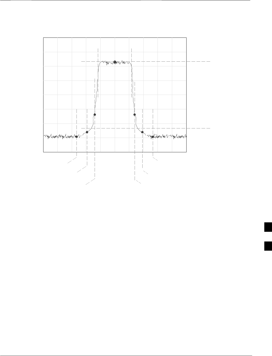
TX Spectral Purity Transmit Mask Acceptance Test – continued
Jun 2004 7-13
1X SC480 BTS Hardware Installation, Optimization/ATP, and FRU
DRAFT
Figure 7-1: TX Mask Verification Spectrum Analyzer Display
– 885 kHz + 885 kHz
Center Frequency Reference
Attenuation level of all
spurious and IM products
with respect to the mean
power of the CDMA channel
.5 MHz Span/Div
Ampl 10 dB/Div
Mean CDMA Bandwidth
Power Reference
– 1980 kHz
+750 kHz
+ 1980 kHz
– 750 kHz
7

TX Waveform Quality (Rho) Acceptance Test
DRAFT
1X SC480 BTS Hardware Installation, Optimization/ATP, and FRU Jun 2004
7-14
Background
Overview – This test verifies the transmitted pilot channel element
digital waveform quality of each operator–selected BBX carrier keyed up
at a specific frequency specified in the current CDF. All tests are
performed using the external, calibrated test equipment controlled by the
same command. All measurements are made at the appropriate TX
antenna connector.
Equipment Operation During Testing – Pilot gain will be set to 262
for each antenna, and all TCH elements from the MCCs will be
forward–link disabled. The selected BBXs will be keyed up using both
bbxlvl and BLO to generate a CDMA carrier (with pilot channel
element only, Walsh code 0). RF output power is set at 40 dBm as
measured at the appropriate BTS TX antenna connector.
Test Measurements – The test equipment will measure and return the
pilot channel element digital waveform quality (rho) percentage,
verifying that the result meets the following specification:
Waveform quality (Rho) should be > 0.98.
Waveform Quality (Rho)
Acceptance Test
Follow the steps in Table 7-6 to verify the pilot channel element
waveform quality (rho) on the TX antenna paths for the selected BBXs.
Table 7-6: Test Waveform Quality (Rho)
Step Action
1Set up the test equipment for TX acceptance tests per Table 7-1.
2Select the BBXs to be tested.
3Click on Tests in the BTS menu bar, and select TX > Rho... from the pull–down menus.
4Select the appropriate carrier(s) and sector(s) (carrier-bts#-sector#-carrier#) from those displayed in the
Channels/Carrier pick list.
NOTE
To select multiple items, hold down the Shift or Ctrl key while clicking on pick list items to select
multiple carrier(s)–sector(s).
5Verify that the correct channel number for the selected carrier is shown in the Carrier # Channels
box.
– If it is not, obtain the latest bts–#.cdf and cbsc–#.cdf files from the CBSC.
NOTE
If necessary, the correct channel number may be manually entered into the Carrier # Channels box.
6 Click OK to display a status bar followed by a Directions pop-up window.
7Follow the cable connection directions as they are displayed, and click the Continue button to begin
testing.
– As the ATP process is completed, results will be displayed in a status report window.
. . . continued on next page
7

TX Waveform Quality (rho) Acceptance Test – continued
Jun 2004 7-15
68P09253A60
1X SC480 BTS Hardware Installation, Optimization/ATP, and FRU
DRAFT
Table 7-6: Test Waveform Quality (Rho)
Step Action
8Click the Save Results or Dismiss button.
NOTE
If Dismiss is used, the test results will not be saved in the test report file.
7

TX Pilot Time Offset Acceptance Test
DRAFT
1X SC480 BTS Hardware Installation, Optimization/ATP, and FRU Jun 2004
7-16
Background
Overview – This test verifies the transmitted pilot channel element Pilot
Time Offset of each operator–selected BBX carrier keyed up at a specific
frequency specified in the current CDF. All tests will be performed using
the external, calibrated test equipment controlled by the same command.
All measurements will be made at the BTS TX antenna connector.
Equipment Operation During Testing – The pilot gain will be set to
262 for each antenna and all TCH elements from the MCCs will be
forward–link disabled. The selected BBXs will be keyed using both
bbxlvl and BLO to generate a CDMA carrier (with pilot channel
element only, Walsh code 0). TX power output is set at 40 dBm as
measured at the TX output.
Test Measurements – The test equipment will measure and return the
Pilot Time Offset in ms, verifying that results meet the following
specification:
Pilot Time Offset should be within 3 ms of the target PT Offset
(zero ms).
This test also executes and returns the TX Frequency and
TX Waveform Quality (rho) ATP tests, however, only Pilot
Time Offset results are written to the ATP test report.
NOTE
Pilot Time Offset Acceptance
Test
Follow the steps in Table 7-7 to verify the Pilot Time Offset on the TX
antenna paths for the selected BBXs.
Table 7-7: Test Pilot Time Offset
Step Action
1Set up the test equipment for TX acceptance tests per Table 7-1.
2Select the BBXs to be tested.
3Click on Tests in the BTS menu bar, and select TX > Pilot Time Offset... from the pull–down menus.
4Select the appropriate carrier(s) and sector(s) (carrier-bts#-sector#-carrier#) from those displayed in the
Channels/Carrier pick list.
NOTE
To select multiple items, hold down the Shift or Ctrl key while clicking on pick list items to select
multiple carrier(s)–sector(s).
. . . continued on next page
7

TX Pilot Time Offset Acceptance Test – continued
Jun 2004 7-17
1X SC480 BTS Hardware Installation, Optimization/ATP, and FRU
DRAFT
Table 7-7: Test Pilot Time Offset
Step Action
5Verify that the correct channel number for the selected carrier is shown in the Carrier # Channels
box.
– If it is not, obtain the latest bts–#.cdf and cbsc–#.cdf files from the CBSC.
NOTE
If necessary, the correct channel number may be manually entered into the Carrier # Channels box.
6 Click OK to display a status bar followed by a Directions pop-up window.
7Follow the cable connection directions as they are displayed, and click the Continue button to begin
testing.
– As the ATP process is completed, results will be displayed in a status report window.
8Click the Save Results or Dismiss button.
NOTE
If Dismiss is used, the test results will not be saved in the test report file.
7

TX Code Domain Power/Noise Floor Acceptance Test
DRAFT
1X SC480 BTS Hardware Installation, Optimization/ATP, and FRU Jun 2004
7-18
Background
Overview – This test verifies the Code Domain Power and Noise Floor
of each operator–selected BBX carrier keyed at a specific frequency
specified in the current CDF. All tests are performed using the external,
calibrated test equipment controlled by the same command. All
measurements are made at the appropriate BTS TX antenna connector.
CDMA Channel Test Set–up – Pilot gain will be set to 262 for each
antenna and the selected MCCs will be configured to supply all
odd–numbered Walsh code traffic channel elements by enabling
Orthogonal Channel Noise Source (OCNS) on all odd MCC channel
elements (maximum 32 full rate channels with an OCNS gain of 81). All
even–numbered Walsh code traffic channel elements will not have
OCNS enabled, and are considered “OFF”. Selected MCCs will be
forward–link enabled for the antenna (sector) under test.
Equipment Operation During Testing – The BBX will be keyed up
using a BLO–corrected bbxlvl value to generate a CDMA carrier
consisting of pilot and OCNS channels. RF output power, as measured at
the appropriate frame TX antenna connector, is set at one of the
following values depending on the operating frequency spectrum:
S800 MHz: 33.5 dBm
Test Measurements – The test equipment will measure and return the
channel element power in dB of all specified Walsh channels within the
CDMA spectrum. Additional calculations will be performed to verify the
following parameters are met (refer to Figure 7-2 for graphic
representations):
STraffic channel element power level will be verified by calculating the
ratio of Pilot power to OCNS gain of all traffic channels (root sum of
the square (RSS) of each OCNS gain divided by the Pilot power).
This value should be 10.2 dB + 2.0 dB.
SNoise floor (unassigned “OFF” even–numbered Walsh channels) is
verified to be < –27 dB for IS–95A/B and CDMA2000 1X with
respect to total CDMA channel power.
Code Domain Power/Noise
Floor Test
Follow the steps in Table 7-8 to verify the Code Domain Power/Noise
floor of each selected BBX carrier keyed up at a specific frequency.
7

TX Code Domain Power/Noise Floor Acceptance Test – continued
Jun 2004 7-19
1X SC480 BTS Hardware Installation, Optimization/ATP, and FRU
DRAFT
Table 7-8: Test Code Domain Power/Noise Floor
Step Action
1Set up the test equipment for TX acceptance tests per Table 7-1.
2Select the BBXs and MCCs to be tested.
3Click on Tests in the BTS menu bar, and select TX > Code Domain Power... from the pull–down
menus.
4Select the appropriate carrier(s) and sector(s) (carrier-bts#-sector#-carrier#) from those displayed in the
Channels/Carrier pick list.
NOTE
To select multiple items, hold down the Shift or Ctrl key while clicking on pick list items to select
multiple carrier(s)–sector(s).
5Verify that the correct channel number for the selected carrier is shown in the Carrier # Channels
box.
– If it is not, obtain the latest bts–#.cdf and cbsc–#.cdf files from the CBSC.
NOTE
If necessary, the correct channel number may be manually entered into the Carrier # Channels box.
6 Click OK to display a status bar followed by a Directions pop-up window.
7Follow the cable connection directions as they are displayed, and click the Continue button to begin
testing.
– As the ATP process is completed, results will be displayed in a status report window.
8Click the Save Results or Dismiss button.
NOTE
If Dismiss is used, the test results will not be saved in the test report file.
7
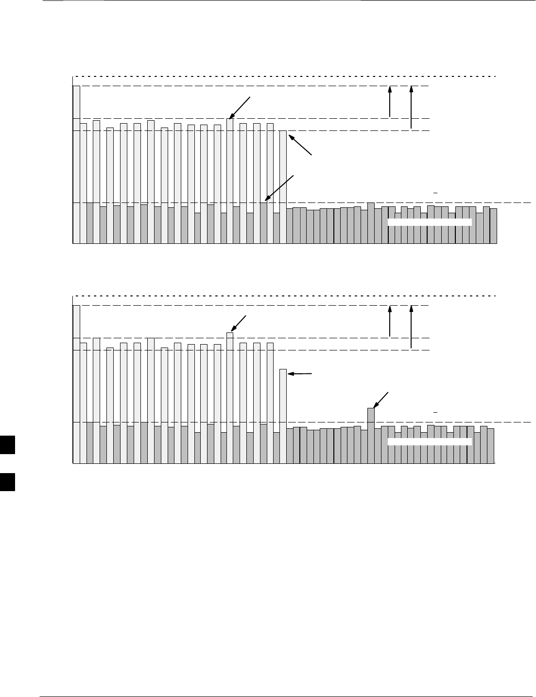
TX Code Domain Power/Noise Floor Acceptance Test – continued
DRAFT
1X SC480 BTS Hardware Installation, Optimization/ATP, and FRU Jun 2004
7-20
Pilot Channel
Active channels
PILOT LEVEL
MAX OCNS SPEC.
MIN OCNS SPEC.
MAXIMUM NOISE FLOOR:
< –27 dB FOR IS–95A/B AND
CDMA2000 1X
Inactive channels
Walsh 0 1 2 3 4 5 6 7 ... 64
MAX OCNS
CHANNEL
MIN OCNS
CHANNEL
8.2 dB 12.2 dB
MAX NOISE
FLOOR
Pilot Channel
Active channels
PILOT LEVEL
MAX OCNS SPEC.
MIN OCNS SPEC.
MAXIMUM NOISE FLOOR:
< –27 dB FOR IS–95A/B AND
CDMA2000 1X
Inactive channels
Walsh 0 1 2 3 4 5 6 7 ... 64
FAILURE – DOES NOT
MEET MIN OCNS SPEC.
FAILURE – EXCEEDS
MAX OCNS SPEC. 8.2 dB 12.2 dB
FAILURE – EXCEEDS MAX
NOISE FLOOR SPEC.
Code Domain Power/Noise Floor (OCNS Pass) Example
Figure 7-2: Code Domain Analyzer CD Power/Noise Floor Display Examples
Code Domain Power/Noise Floor (OCNS Failure) Example
7

RX FER Acceptance Test
Jun 2004 7-21
1X SC480 BTS Hardware Installation, Optimization/ATP, and FRU
DRAFT
Background
Overview – This test verifies the BTS Frame Erasure Rate (FER) on all
TCHs currently configured on operator–selected MCCs (fullrate at 1%
FER) at –119 dBm. All tests are performed using the external, calibrated
test equipment as the signal source controlled by the same command.
Measurements are made at the specified BTS RX antenna connection.
Equipment Operation During Testing – The pilot gain on each MCC
will be set to 262 for each TX antenna, and the forward link for all TCH
elements from the MCCs will be enabled. Appropriate BBX(s) must be
keyed in order to enable the RX receive circuitry. Operator–selected
BBXs will be keyed using only bbxlvl, to generate a CDMA carrier
with pilot channel element only. Transmit power output is set at –40
dBm. Test equipment output power is set so that the received power at
the BBX is –119 dBm. The final output power setting of the test
equipment takes into account the MPC type, BTS RF path losses, and
test cable losses. .
Test Measurements – The LMF will prompt the MCC channel element
under test to measure all–zero longcode and provide the FER report on
the selected active MCC on the reverse link for the main and, if selected,
diversity RX antenna paths. Results are evaluated to ensure they meet
the following specification:
FER returned less than 1% and Total Frames measured is 1500
FER Acceptance Test
Follow the steps in Table 7-9 to verify the FER on RX antenna paths
using selected MCCs and BBXs.
Table 7-9: Test FER
Step Action
1Set up the test equipment for RX acceptance tests per Table 7-1.
2* IMPORTANT
If the LMF has been logged into the BTS with a different Multi–Channel Preselector setting than the
one to be used for this test, the LMF must be logged out of the BTS and logged in again with the new
Multi–Channel Preselector setting. Using the wrong MPC setting can cause a false test failure.
3Select the BBXs and MCCs to be tested.
4Click on Tests in the BTS menu bar, and select RX > FER... from the pull–down menu.
5Select the appropriate carrier(s) and sector(s) (carrier-bts#-sector#-carrier#) from those displayed in the
Channels/Carrier pick list.
6NOTE
To select multiple items, hold down the Shift or Ctrl key while clicking on pick list items to select
multiple carrier(s)–sector(s).
. . . continued on next page
7

RX FER Acceptance Test – continued
DRAFT
1X SC480 BTS Hardware Installation, Optimization/ATP, and FRU Jun 2004
7-22
Table 7-9: Test FER
Step Action
7Verify that the correct channel number for the selected carrier is shown in the Carrier # Channels
box.
– If it is not, obtain the latest bts–#.cdf and cbsc–#.cdf files from the CBSC.
8NOTE
If necessary, the correct channel number may be manually entered into the Carrier # Channels box.
9* IMPORTANT
If a companion frame with the inter–frame diversity RX cabling disconnected is being tested do not
select BOTH in this step. The RX main and diversity paths must be tested separately for this
configuration because each requires a different Multi–Coupler Preselector type to provide the proper
test signal gain.
10 Select the appropriate RX branch (Both, Main, or Diversity) in the drop–down list.
11 In the Rate Set box, select the appropriate data rate (1=9600, 2=14400, 3=9600 1X) from the
drop–down list.
12 NOTE
The Rate Set selection of 3 is only available if 1X cards are selected for the test.
13 Click OK to display a status bar followed by a Directions pop-up window.
14 Follow cable connection directions as they are displayed, and click the Continue button to begin
testing.
– As the ATP process is completed, results will be displayed in the status report window.
15 Click the Save Results or Dismiss button.
NOTE
If Dismiss is used, the test results will not be saved in the test report file.
7

Generating an ATP Report
Jun 2004 7-23
1X SC480 BTS Hardware Installation, Optimization/ATP, and FRU
DRAFT
Background
Each time an ATP test is run, ATP data is updated and must be saved to
an ATP report file using the Save Results button to close the status
report window. The ATP report file will not be updated if the status
reports window is closed using the Dismiss button.
ATP Report
A separate report is created for each BTS and includes the following for
each test:
STest name
SPASS or FAIL
SDescription information (if applicable)
SBBX number
SChannel number
SCarrier number
SSector number
SUpper test limit
SLower test limit
STest result
STime stamp
SDetails/Warning information (if applicable)
Follow the procedures in the Table 7-10 to view and create a printable
file for the ATP report.
Table 7-10: Generating an ATP Report
Step Action
1Click on the Login tab (if not in the forefront).
2Click on the desired BTS in the Available Base Stations pick list to select it.
3Click on the Report button.
4If a printable file is not needed, click on the Dismiss button.
5If a printable file is required, perform the following:
5a – Select the desired file type (text, comma–delimited, HTML) for the report file from the
drop–down list at the bottom of the screen.
5b – Click the Save button to save the file.
–– The file will be saved in the selected format in the bts–# folder for the BTS selected.
7

Generating an ATP Report – continued
DRAFT
1X SC480 BTS Hardware Installation, Optimization/ATP, and FRU Jun 2004
7-24
Notes
7

Jun 2004 1X SC480 BTS Hardware Installation, Optimization/ATP, and FRU
DRAFT
Chapter 8: Leave the Site
Table of Contents
Updating Calibration Data Files 8-1 . . . . . . . . . . . . . . . . . . . . . . . . . . . . . . . . . . . . .
Software Release caveats 8-1 . . . . . . . . . . . . . . . . . . . . . . . . . . . . . . . . . . . .
Copy and Load Cal File to to CBSC 8-1 . . . . . . . . . . . . . . . . . . . . . . . . . . .
Prepare to Leave the Site 8-3 . . . . . . . . . . . . . . . . . . . . . . . . . . . . . . . . . . . . . . . . . .
External Test Equipment Removal 8-3 . . . . . . . . . . . . . . . . . . . . . . . . . . . .
Bringing Modules into Service with the LMF 8-3 . . . . . . . . . . . . . . . . . . .
WinLMF Removal 8-4 . . . . . . . . . . . . . . . . . . . . . . . . . . . . . . . . . . . . . . . . .
Connecting BTS T1/E1 Spans 8-4 . . . . . . . . . . . . . . . . . . . . . . . . . . . . . . . .
Final Checks before leaving site 8-5 . . . . . . . . . . . . . . . . . . . . . . . . . . . . . .
Reset All Devices and Initialize Site Remotely 8-5 . . . . . . . . . . . . . . . . . . .
8

Table of Contents – continued
1X SC480 BTS Hardware Installation, Optimization/ATP, and FRU Jun 2004
DRAFT
Notes
8

Updating Calibration Data Files
Jun 2004 1X SC480 BTS Hardware Installation, Optimization/ATP, and FRU 8-1
DRAFT
Software Release caveats
With Software Release 2.16.1.x, the packet BTS will NOT detect a new
calibration file on the OMC–R. A manual workaround is available in
bulletin cdma_g_bts_059. This will be corrected in Software Release
2.16.3.
Software Release 2.16.3 will allow the user to load the calibration file
from the LMF directly onto the MGLI. The MGLI will then ftp the new
calibration file to the OMC–R, thereby eliminating the need for the user
to place the calibration file at the OMC–R.
Copy and Load Cal File to to
CBSC
After completing the TX calibration and audit, updated CAL file
information must be moved from the LMF Windows environment back
to the CBSC, a Unix environment. The following procedures detail
moving files from one environment to the other.
Copying CAL files from LMF to a Diskette
Follow the procedures in Table 8-1 to copy the CAL files from an LMF
computer to a 3.5 diskette.
Table 8-1: Copying CAL Files to a Diskette
Step Action
1 With Windows running on the LMF computer, insert a disk into Drive A:\.
2Launch the Windows Explorer application program from the Start > Programs menu list.
3Select the applicable <x>:\<lmf home directory/cdma/bts–# folder.
4Drag the bts–#.cal file to Drive A.
5Repeat Steps 3 and 4, as required, for other bts–# folders.
8

Updating Calibration Data Files – continued
8-2 1X SC480 BTS Hardware Installation, Optimization/ATP, and FRU Jun 2004
DRAFT
Copying CAL Files from Diskette to the CBSC
Follow the procedures in Table 8-2 to copy CAL files from a diskette to
the CBSC.
Table 8-2: Copying CAL Files from Diskette to the CBSC
Step Action
1Log into the CBSC on the OMC–R Unix workstation using your account name and password.
2Place the diskette containing calibration files (cal files) in the workstation diskette drive.
3Type in eject –q and press the Enter key.
4 Enter mount and press the Enter key. Verify that floppy/no_name is displayed.
NOTE
If the eject command has been previously entered, floppy/no_name will be appended with a
number. Use the explicit floppy/no_name reference displayed.
5Type in cd /floppy/no_name and press the Enter key.
6Type in ls –lia and press the Enter key. Verify the bts–#.cal file filename appears in the displayed
directory listing.
7Type in cd and press the Enter key.
8Type in pwd and press the Enter key. Verify the displayed response shows the correct home
directory (/home/<user’s name>).
9 With Solaris versions of Unix, create a Unix–formatted version of the bts–#.cal file in the home
directory by performing the following:
9a – Type in dos2unix /floppy/no_name/bts–#.cal bts–#.cal and press the Enter key.
Where: # = BTS number for which the CAL file was created
NOTE
Other versions of Unix do not support the dos2unix command. In these cases, use the Unix cp
(copy) command. The copied files will contain DOS line feed characters which must be edited out
with a Unix text editor.
10 Type in ls –l *.cal and press the Enter key. Verify the CAL files have been copied. Verify all CAL
files to be transferred appear in the displayed listing.
11 Type eject and press the Enter key.
12 Remove the diskette from the workstation.
8
Prepare to Leave the Site
Jun 2004 1X SC480 BTS Hardware Installation, Optimization/ATP, and FRU 8-3
DRAFT
External Test Equipment
Removal Perform the procedure in Table 8-3 to disconnect the test equipment and
configure the BTS for active service.
Table 8-3: Remove External Test Equipment
Step Action
1n WARNING
Be sure no BBXs are keyed before performing this step. Failure to do so can result in personal injury
and damage to BTS LPAs.
Disconnect all external test equipment from all TX and RX connectors at the rear of the frame.
2Reconnect and visually inspect all TX and RX antenna feed lines at the frame RF interface panel.
NOTE
Verify that all sector antenna feed lines are connected to the correct antenna connectors on the frame.
Crossed antenna cables will degrade call processing.
Bringing Modules into Service
with the LMF
Whenever possible, have the CBSC/MM bring up the site
and enable all devices at the BTS.
NOTE
If there is a reason code and/or data should or could not be loaded
remotely from the CBSC, follow the steps outlined in Table 8-4 as
required to bring BTS processor modules from OOS to INS state.
Table 8-4: Bring Modules into Service
Step Action
1In the WinLMF GUI environment, select the device(s) to be enabled by clicking on each one.
NOTE
SThe GLI and CSA must be INS_ACT (bright green) before an MCC can be enabled.
SProcessors which must be enabled and the order of enabling are as follows:
1. GLI
2. CSA
3. MCCs
2Click on Device in the BTS menu bar, and select Enable from the pull–down list.
– A status report window is displayed.
3NOTE
If a BBX is selected, a transceiver parameters window is displayed to collect keying information. Do
not enable the BBX.
. . . continued on next page
8

Prepare to Leave the Site – continued
8-4 1X SC480 BTS Hardware Installation, Optimization/ATP, and FRU Jun 2004
DRAFT
Table 8-4: Bring Modules into Service
Step Action
4 Click Cancel to close the transceiver parameters window, if applicable.
5 Click OK to close the status report window.
– The color of devices which successfully change to INS will change bright green.
WinLMF Removal
Perform the procedure in Table 8-5 as required to terminate the WinLMF
GUI session and remove the WinLMF computer.
Table 8-5: Terminate the WinLMF Session and Remove the WinLMF
Step Action
1! CAUTION
Do not power down the WinLMF terminal without performing the procedure below. Corrupted/lost
data files may result.
Log out of all BTS sessions and exit WinLMF by clicking on File in the WinLMF window menu bar and
selecting Logout and Exit from the pull–down list.
2In the Windows Task Bar, click Start and select Shutdown. Click Yes when the Shut Down Windows
message appears.
3Wait for the system to shut down and the screen to go blank.
4Disconnect the WinLMF terminal Ethernet port from the BTS frame.
5Disconnect the WinLMF terminal serial port, the RS–232–to–GPIB interface box, and the GPIB
cables as required for equipment transport.
Connecting BTS T1/E1 Spans
Perform the procedure in Table 8-6 to connect any T1 or E1 span
connectors removed previously to allow the WinLMF to control the
BTS.
Table 8-6: Connect T1 or E1 Spans
Step Action
1Re–connect any disconnected span lines.
2Verify span status, ensuring the OMC–R/CBSC can communicate with the BTS.
8

Prepare to Leave the Site – continued
Jun 2004 1X SC480 BTS Hardware Installation, Optimization/ATP, and FRU 8-5
DRAFT
Final Checks before leaving
site
Be sure all requirements listed in Table 8-7 are completed before leaving
the site.
Table 8-7: Check Before Leaving the Site
Step Action
1When backup batteries are installed, all battery circuit breakers are ON (pushed in).
2BTS circuit breaker is ON (pushed in).
3No alarm conditions are being reported to the OMC–R.
Reset All Devices and Initialize
Site Remotely
Devices in the BTS should not be left with data and code loaded from
the WinLMF. The configuration data and code loads used for normal
operation could be different from those stored in the WinLMF files.
Perform the procedure in Table 8-8 to reset all devices and initialize site
remotely.
Table 8-8: Reset BTS Devices and Remote Site Initialization
Step Action
1Terminate the WinLMF session by following the procedures in Table 8-5.
2Reconnect spans by following the procedure in Table 8-6.
3Circuit BTS Procedure:
3a From the BTS site, contact the OMC–R and request the operator to perform a BTS reset.
or
At the BTS site:
– unseat the GLI card and wait for 30 seconds;
3b Have the operator perform the following:
SACTIVATE the GLI to set the Nextload attribute for the GLI to the one for the current BSS
software version;
SDisable the GLI;
SEnable the GLI to allow the MM to load the software version specified by the Nextload
attribute;
SOnce the GLI is INS_ACT, contact the OMC–R and request the operator ACTIVATE the BTS.
– Once the GLI card is loaded with the specified code version, the GLI will verify and update, as
required, the RAM and, if it is necessary, ROM code loads for the installed CSA, MCC, and BBX
cards using the DLM.
4After all activities at the site have been completed, contact the OMC–R and confirm that the BTS is
under OMC–R control.
8

Prepare to Leave the Site – continued
8-6 1X SC480 BTS Hardware Installation, Optimization/ATP, and FRU Jun 2004
DRAFT
Notes
8

Jun 2004 1X SC480 BTS Hardware Installation, Optimization/ATP, and FRU
DRAFT
Chapter 9: Field Replaceable Unit
Table of Contents
Introduction 9-1 . . . . . . . . . . . . . . . . . . . . . . . . . . . . . . . . . . . . . . . . . . . . . . . . . . . . .
Scope 9-1 . . . . . . . . . . . . . . . . . . . . . . . . . . . . . . . . . . . . . . . . . . . . . . . . . . .
Section Organization 9-1 . . . . . . . . . . . . . . . . . . . . . . . . . . . . . . . . . . . . . . .
Fan Module 9-4 . . . . . . . . . . . . . . . . . . . . . . . . . . . . . . . . . . . . . . . . . . . . . . . . . . . . .
Introduction 9-4 . . . . . . . . . . . . . . . . . . . . . . . . . . . . . . . . . . . . . . . . . . . . . .
System Impact/Considerations 9-4 . . . . . . . . . . . . . . . . . . . . . . . . . . . . . . .
Required Items 9-4 . . . . . . . . . . . . . . . . . . . . . . . . . . . . . . . . . . . . . . . . . . . .
Prerequisite 9-4 . . . . . . . . . . . . . . . . . . . . . . . . . . . . . . . . . . . . . . . . . . . . . .
Replacement Procedure 9-5 . . . . . . . . . . . . . . . . . . . . . . . . . . . . . . . . . . . . .
High and Medium Stability Oscillator Module 9-7 . . . . . . . . . . . . . . . . . . . . . . . . .
Introduction 9-7 . . . . . . . . . . . . . . . . . . . . . . . . . . . . . . . . . . . . . . . . . . . . . .
System Impact/Considerations 9-7 . . . . . . . . . . . . . . . . . . . . . . . . . . . . . . .
Front Panel Indicator 9-7 . . . . . . . . . . . . . . . . . . . . . . . . . . . . . . . . . . . . . . .
Required Items 9-7 . . . . . . . . . . . . . . . . . . . . . . . . . . . . . . . . . . . . . . . . . . . .
Prerequisite 9-7 . . . . . . . . . . . . . . . . . . . . . . . . . . . . . . . . . . . . . . . . . . . . . .
Replacement Procedure 9-8 . . . . . . . . . . . . . . . . . . . . . . . . . . . . . . . . . . . . .
Global Positioning System (GPS) Receivers 9-11 . . . . . . . . . . . . . . . . . . . . . . . . . . .
Introduction 9-11 . . . . . . . . . . . . . . . . . . . . . . . . . . . . . . . . . . . . . . . . . . . . . .
System Impact/Considerations 9-11 . . . . . . . . . . . . . . . . . . . . . . . . . . . . . . .
Required Items 9-11 . . . . . . . . . . . . . . . . . . . . . . . . . . . . . . . . . . . . . . . . . . . .
Prerequisite 9-11 . . . . . . . . . . . . . . . . . . . . . . . . . . . . . . . . . . . . . . . . . . . . . .
Replacement Procedure 9-11 . . . . . . . . . . . . . . . . . . . . . . . . . . . . . . . . . . . . .
RF–GPS Module 9-14 . . . . . . . . . . . . . . . . . . . . . . . . . . . . . . . . . . . . . . . . . . . . . . . . .
Introduction 9-14 . . . . . . . . . . . . . . . . . . . . . . . . . . . . . . . . . . . . . . . . . . . . . .
System Impact/Considerations 9-14 . . . . . . . . . . . . . . . . . . . . . . . . . . . . . . .
Required Items 9-14 . . . . . . . . . . . . . . . . . . . . . . . . . . . . . . . . . . . . . . . . . . . .
Prerequisite 9-14 . . . . . . . . . . . . . . . . . . . . . . . . . . . . . . . . . . . . . . . . . . . . . .
Replacement Procedure 9-14 . . . . . . . . . . . . . . . . . . . . . . . . . . . . . . . . . . . . .
Power Supply Module (PSM) 9-18 . . . . . . . . . . . . . . . . . . . . . . . . . . . . . . . . . . . . . . .
Introduction 9-18 . . . . . . . . . . . . . . . . . . . . . . . . . . . . . . . . . . . . . . . . . . . . . .
System Impact/Consideration 9-18 . . . . . . . . . . . . . . . . . . . . . . . . . . . . . . . .
Required Items 9-18 . . . . . . . . . . . . . . . . . . . . . . . . . . . . . . . . . . . . . . . . . . . .
Prerequisite 9-18 . . . . . . . . . . . . . . . . . . . . . . . . . . . . . . . . . . . . . . . . . . . . . .
Replacement Procedure 9-19 . . . . . . . . . . . . . . . . . . . . . . . . . . . . . . . . . . . . .
Clock Synchronization Alarms Card 9-21 . . . . . . . . . . . . . . . . . . . . . . . . . . . . . . . . .
Introduction 9-21 . . . . . . . . . . . . . . . . . . . . . . . . . . . . . . . . . . . . . . . . . . . . . .
9

Table of Contents – continued
1X SC480 BTS Hardware Installation, Optimization/ATP, and FRU Jun 2004
DRAFT
System Impact/Considerations 9-21 . . . . . . . . . . . . . . . . . . . . . . . . . . . . . . .
Required Items 9-21 . . . . . . . . . . . . . . . . . . . . . . . . . . . . . . . . . . . . . . . . . . . .
Prerequisite 9-21 . . . . . . . . . . . . . . . . . . . . . . . . . . . . . . . . . . . . . . . . . . . . . .
Replacement Procedure 9-21 . . . . . . . . . . . . . . . . . . . . . . . . . . . . . . . . . . . . .
Group Line Interface Card 9-24 . . . . . . . . . . . . . . . . . . . . . . . . . . . . . . . . . . . . . . . . .
Introduction 9-24 . . . . . . . . . . . . . . . . . . . . . . . . . . . . . . . . . . . . . . . . . . . . . .
System Impact/Considerations 9-24 . . . . . . . . . . . . . . . . . . . . . . . . . . . . . . .
Prerequisite 9-24 . . . . . . . . . . . . . . . . . . . . . . . . . . . . . . . . . . . . . . . . . . . . . .
Required Items 9-24 . . . . . . . . . . . . . . . . . . . . . . . . . . . . . . . . . . . . . . . . . . . .
Replacement Procedure 9-24 . . . . . . . . . . . . . . . . . . . . . . . . . . . . . . . . . . . . .
Optimization Requirement 9-26 . . . . . . . . . . . . . . . . . . . . . . . . . . . . . . . . . . .
Multi–Channel CDMA Card 9-28 . . . . . . . . . . . . . . . . . . . . . . . . . . . . . . . . . . . . . . .
Introduction 9-28 . . . . . . . . . . . . . . . . . . . . . . . . . . . . . . . . . . . . . . . . . . . . . .
System Impact/Considerations 9-28 . . . . . . . . . . . . . . . . . . . . . . . . . . . . . . .
MCC Front Panel 9-28 . . . . . . . . . . . . . . . . . . . . . . . . . . . . . . . . . . . . . . . . . .
Required Items 9-28 . . . . . . . . . . . . . . . . . . . . . . . . . . . . . . . . . . . . . . . . . . . .
Prerequisite 9-29 . . . . . . . . . . . . . . . . . . . . . . . . . . . . . . . . . . . . . . . . . . . . . .
Replacement Procedure 9-29 . . . . . . . . . . . . . . . . . . . . . . . . . . . . . . . . . . . . .
Optimization Requirement 9-30 . . . . . . . . . . . . . . . . . . . . . . . . . . . . . . . . . . .
Broadband Transceiver Card 9-32 . . . . . . . . . . . . . . . . . . . . . . . . . . . . . . . . . . . . . . . .
Introduction 9-32 . . . . . . . . . . . . . . . . . . . . . . . . . . . . . . . . . . . . . . . . . . . . . .
System Impact/ Considerations 9-32 . . . . . . . . . . . . . . . . . . . . . . . . . . . . . . .
Front Panel 9-32 . . . . . . . . . . . . . . . . . . . . . . . . . . . . . . . . . . . . . . . . . . . . . . .
Required items 9-33 . . . . . . . . . . . . . . . . . . . . . . . . . . . . . . . . . . . . . . . . . . . .
Prerequisite 9-33 . . . . . . . . . . . . . . . . . . . . . . . . . . . . . . . . . . . . . . . . . . . . . .
Replacement Procedure 9-33 . . . . . . . . . . . . . . . . . . . . . . . . . . . . . . . . . . . . .
Optimization Requirement 9-34 . . . . . . . . . . . . . . . . . . . . . . . . . . . . . . . . . . .
Compact BTS Multi–Coupler Preselector Card 9-36 . . . . . . . . . . . . . . . . . . . . . . . . .
Introduction 9-36 . . . . . . . . . . . . . . . . . . . . . . . . . . . . . . . . . . . . . . . . . . . . . .
System Impact/Considerations 9-36 . . . . . . . . . . . . . . . . . . . . . . . . . . . . . . .
Required items 9-36 . . . . . . . . . . . . . . . . . . . . . . . . . . . . . . . . . . . . . . . . . . . .
Prerequisite 9-36 . . . . . . . . . . . . . . . . . . . . . . . . . . . . . . . . . . . . . . . . . . . . . .
Replacement Procedure 9-37 . . . . . . . . . . . . . . . . . . . . . . . . . . . . . . . . . . . . .
MCC Data Only (MCC–DO) Card 9-41 . . . . . . . . . . . . . . . . . . . . . . . . . . . . . . . . . . .
Introduction 9-41 . . . . . . . . . . . . . . . . . . . . . . . . . . . . . . . . . . . . . . . . . . . . . .
EV–DO FRU Information 9-41 . . . . . . . . . . . . . . . . . . . . . . . . . . . . . . . . . . .
System Impact/Considerations 9-41 . . . . . . . . . . . . . . . . . . . . . . . . . . . . . . .
LED States 9-41 . . . . . . . . . . . . . . . . . . . . . . . . . . . . . . . . . . . . . . . . . . . . . . .
Required Items 9-42 . . . . . . . . . . . . . . . . . . . . . . . . . . . . . . . . . . . . . . . . . . . .
Prerequisite 9-42 . . . . . . . . . . . . . . . . . . . . . . . . . . . . . . . . . . . . . . . . . . . . . .
Replacement Procedure 9-42 . . . . . . . . . . . . . . . . . . . . . . . . . . . . . . . . . . . . .
Compact BTS Input and Output Board 9-45 . . . . . . . . . . . . . . . . . . . . . . . . . . . . . . .
Introduction 9-45 . . . . . . . . . . . . . . . . . . . . . . . . . . . . . . . . . . . . . . . . . . . . . .
System Impact/Considerations 9-45 . . . . . . . . . . . . . . . . . . . . . . . . . . . . . . .
CBIO Indicators 9-45 . . . . . . . . . . . . . . . . . . . . . . . . . . . . . . . . . . . . . . . . . . .
Required Items 9-46 . . . . . . . . . . . . . . . . . . . . . . . . . . . . . . . . . . . . . . . . . . . .
9

Table of Contents – continued
Jun 2004 1X SC480 BTS Hardware Installation, Optimization/ATP, and FRU
DRAFT
Prerequisite 9-46 . . . . . . . . . . . . . . . . . . . . . . . . . . . . . . . . . . . . . . . . . . . . . .
Replacement Procedure 9-46 . . . . . . . . . . . . . . . . . . . . . . . . . . . . . . . . . . . . .
SDCX Module 9-50 . . . . . . . . . . . . . . . . . . . . . . . . . . . . . . . . . . . . . . . . . . . . . . . . . .
Introduction 9-50 . . . . . . . . . . . . . . . . . . . . . . . . . . . . . . . . . . . . . . . . . . . . . .
System Impact/Considerations 9-50 . . . . . . . . . . . . . . . . . . . . . . . . . . . . . . .
Required Items 9-50 . . . . . . . . . . . . . . . . . . . . . . . . . . . . . . . . . . . . . . . . . . . .
Prerequisite 9-50 . . . . . . . . . . . . . . . . . . . . . . . . . . . . . . . . . . . . . . . . . . . . . .
Replacement Procedure 9-50 . . . . . . . . . . . . . . . . . . . . . . . . . . . . . . . . . . . . .
RF Filter Tray 9-55 . . . . . . . . . . . . . . . . . . . . . . . . . . . . . . . . . . . . . . . . . . . . . . . . . . .
Introduction 9-55 . . . . . . . . . . . . . . . . . . . . . . . . . . . . . . . . . . . . . . . . . . . . . .
System Impact/Considerations 9-55 . . . . . . . . . . . . . . . . . . . . . . . . . . . . . . .
Required Items 9-55 . . . . . . . . . . . . . . . . . . . . . . . . . . . . . . . . . . . . . . . . . . . .
Prerequisite 9-55 . . . . . . . . . . . . . . . . . . . . . . . . . . . . . . . . . . . . . . . . . . . . . .
Replacement Procedure 9-55 . . . . . . . . . . . . . . . . . . . . . . . . . . . . . . . . . . . . .
Filter Tray Kit SGLN6221 Removal Procedure 9-56 . . . . . . . . . . . . . . . . . .
cMPC Cable Clip Removal Procedure 9-57 . . . . . . . . . . . . . . . . . . . . . . . . .
cMPC Cable Clip Installation Procedure 9-58 . . . . . . . . . . . . . . . . . . . . . . . .
Install Filter Tray Kit SGLN6221 9-58 . . . . . . . . . . . . . . . . . . . . . . . . . . . . .
Filter Tray Kit SGLN6220 Removal Procedure 9-61 . . . . . . . . . . . . . . . . . .
Install Filter Tray Kit SGLN6220 9-63 . . . . . . . . . . . . . . . . . . . . . . . . . . . . .
Filter Tray Kit SGLN6219 Removal Procedure 9-64 . . . . . . . . . . . . . . . . . .
Install Filter Tray Kit SGLN6219 9-65 . . . . . . . . . . . . . . . . . . . . . . . . . . . . .
Compact Combined Linear Power Amplifier 9-67 . . . . . . . . . . . . . . . . . . . . . . . . . . .
Introduction 9-67 . . . . . . . . . . . . . . . . . . . . . . . . . . . . . . . . . . . . . . . . . . . . . .
System Impact/Considerations 9-67 . . . . . . . . . . . . . . . . . . . . . . . . . . . . . . .
Required Items 9-67 . . . . . . . . . . . . . . . . . . . . . . . . . . . . . . . . . . . . . . . . . . . .
Prerequisite 9-67 . . . . . . . . . . . . . . . . . . . . . . . . . . . . . . . . . . . . . . . . . . . . . .
Replacement Procedure 9-67 . . . . . . . . . . . . . . . . . . . . . . . . . . . . . . . . . . . . .
TME Power Distribution Assembly 9-70 . . . . . . . . . . . . . . . . . . . . . . . . . . . . . . . . . .
Introduction 9-70 . . . . . . . . . . . . . . . . . . . . . . . . . . . . . . . . . . . . . . . . . . . . . .
System Impact/Considerations 9-70 . . . . . . . . . . . . . . . . . . . . . . . . . . . . . . .
Required Items 9-70 . . . . . . . . . . . . . . . . . . . . . . . . . . . . . . . . . . . . . . . . . . . .
Prerequisite 9-70 . . . . . . . . . . . . . . . . . . . . . . . . . . . . . . . . . . . . . . . . . . . . . .
Replacement Procedure 9-71 . . . . . . . . . . . . . . . . . . . . . . . . . . . . . . . . . . . . .
Heat Management System 9-74 . . . . . . . . . . . . . . . . . . . . . . . . . . . . . . . . . . . . . . . . .
Introduction 9-74 . . . . . . . . . . . . . . . . . . . . . . . . . . . . . . . . . . . . . . . . . . . . . .
System Impact/Considerations 9-74 . . . . . . . . . . . . . . . . . . . . . . . . . . . . . . .
Required Items 9-74 . . . . . . . . . . . . . . . . . . . . . . . . . . . . . . . . . . . . . . . . . . . .
Periodic Maintenance 9-74 . . . . . . . . . . . . . . . . . . . . . . . . . . . . . . . . . . . . . .
Prerequisite 9-74 . . . . . . . . . . . . . . . . . . . . . . . . . . . . . . . . . . . . . . . . . . . . . .
Replacement Procedure 9-75 . . . . . . . . . . . . . . . . . . . . . . . . . . . . . . . . . . . . .
Heater Element Replacement Procedure 9-77 . . . . . . . . . . . . . . . . . . . . . . . .
Heater Element Installation Procedure 9-77 . . . . . . . . . . . . . . . . . . . . . . . . .
HMS Controller Replacement Procedure 9-78 . . . . . . . . . . . . . . . . . . . . . . .
HMS Controller Installation Procedure 9-78 . . . . . . . . . . . . . . . . . . . . . . . . .
Blower Fan Replacement Procedure 9-79 . . . . . . . . . . . . . . . . . . . . . . . . . . .
9

Table of Contents – continued
1X SC480 BTS Hardware Installation, Optimization/ATP, and FRU Jun 2004
DRAFT
Blower Fan Installation Procedure 9-80 . . . . . . . . . . . . . . . . . . . . . . . . . . . .
Thermal Management Enclosure 9-82 . . . . . . . . . . . . . . . . . . . . . . . . . . . . . . . . . . . .
Introduction 9-82 . . . . . . . . . . . . . . . . . . . . . . . . . . . . . . . . . . . . . . . . . . . . . .
System Impact/Considerations 9-82 . . . . . . . . . . . . . . . . . . . . . . . . . . . . . . .
Required Items 9-82 . . . . . . . . . . . . . . . . . . . . . . . . . . . . . . . . . . . . . . . . . . . .
Prerequisite 9-82 . . . . . . . . . . . . . . . . . . . . . . . . . . . . . . . . . . . . . . . . . . . . . .
Replacement Procedure 9-82 . . . . . . . . . . . . . . . . . . . . . . . . . . . . . . . . . . . . .
Power Distribution Enclosure 9-85 . . . . . . . . . . . . . . . . . . . . . . . . . . . . . . . . . . . . . . .
Introduction 9-85 . . . . . . . . . . . . . . . . . . . . . . . . . . . . . . . . . . . . . . . . . . . . . .
System Impact/Considerations 9-85 . . . . . . . . . . . . . . . . . . . . . . . . . . . . . . .
Replacement Procedure 9-85 . . . . . . . . . . . . . . . . . . . . . . . . . . . . . . . . . . . . .
Master Item Number Failure List 9-86 . . . . . . . . . . . . . . . . . . . . . . . . . . . . . . . . . . . .
Introduction 9-86 . . . . . . . . . . . . . . . . . . . . . . . . . . . . . . . . . . . . . . . . . . . . . .
9

Introduction
Jun 2004 1X SC480 BTS Hardware Installation, Optimization/ATP, and FRU 9-1
DRAFT
Scope
The objective of the Field Replaceable Unit (FRU ) section contains
OMC–R procedures and information and procedures for disassembling
and/or replacing cards, modules, and components of the Compact BTS.
The Compact BTS is a single cage, non–redundant configuration.
Section Organization
The FRU section is organized in the following manner:
SCompact BTS FRU procedures that are performed by a technician at
the site
SOMC–R procedures performed by the operator
BTS FRU Procedures
The BTS FRU procedures are grouped by major functional areas within
the BTS and presented as follows:
SCompact BTS Input/Output (CBIO) Board Replacement Procedure
– Synchronization Daisy–Chaining and eXpansion (SDCX) Module
Replacement Procedure
– RF GPS Module Replacement Procedure
SCCP2 Card and Shelf Replacement Procedures
SRF Component Replacement Procedures
SHigh Stability Oscillator/Medium Stability Oscillator (HSO/MSO)
Replacement Procedure
External Components – The following external components are
optional
SCompact Combined Linear Power Amplifier (cCLPA) Replacement
Procedure
OMC–R Procedures
Describes procedures that can be performed only by the operator from
the OMC–R site.
If the OMC–R operator is unable to resolve the problem, then the user
will be directed to the appropriate section of the Troubleshooting manual
for further action.
9
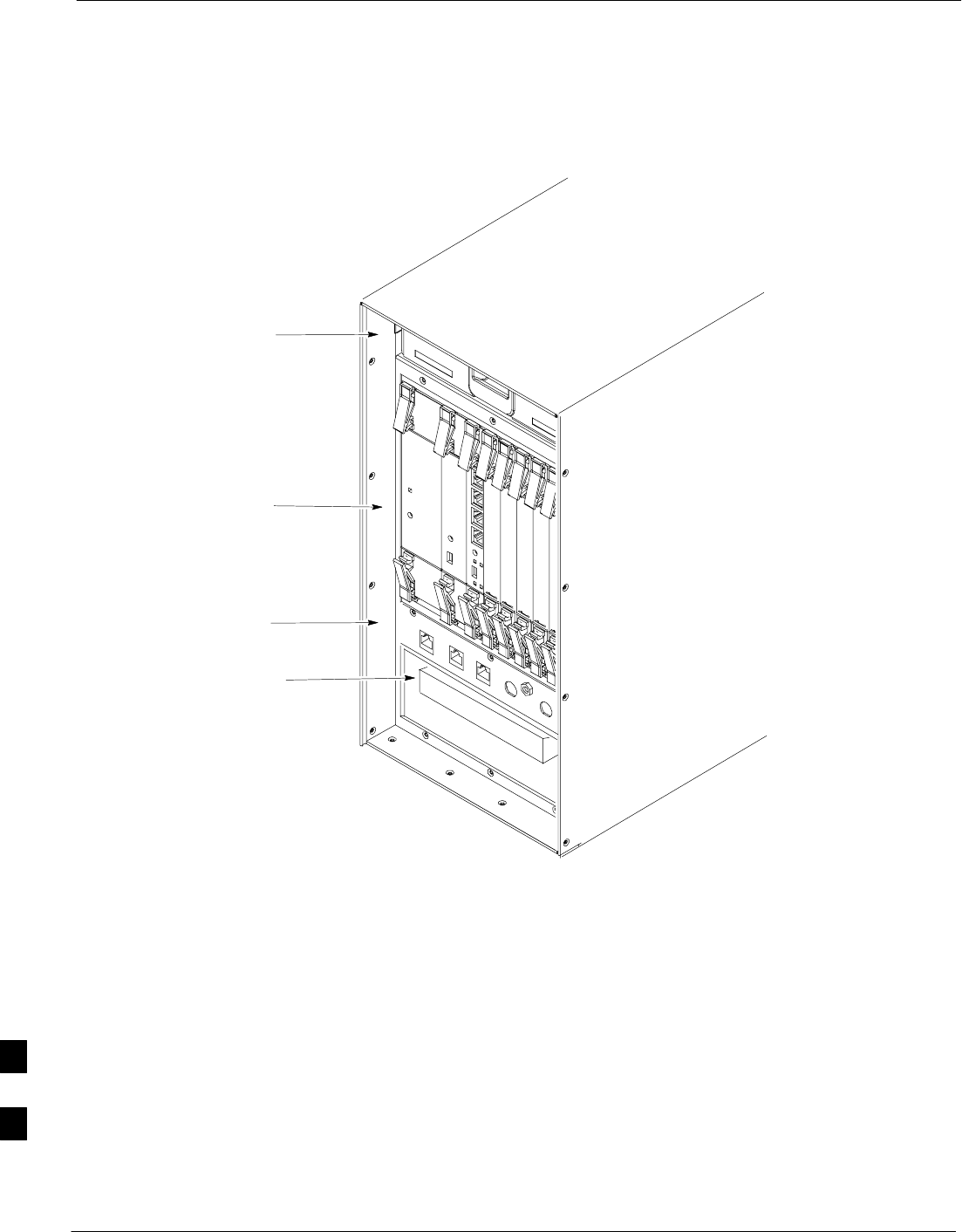
Introduction – continued
9-2 1X SC480 BTS Hardware Installation, Optimization/ATP, and FRU Jun 2004
DRAFT
Figure 9-1: Compact BTS Front Panel Layout without Front Panel Cover
CCP2 Shelf
Fan
Connector Panel
HSO or MSO Module
HSO Module cover
panel removed
NOTE:
Front cover panel is
not shown.
9
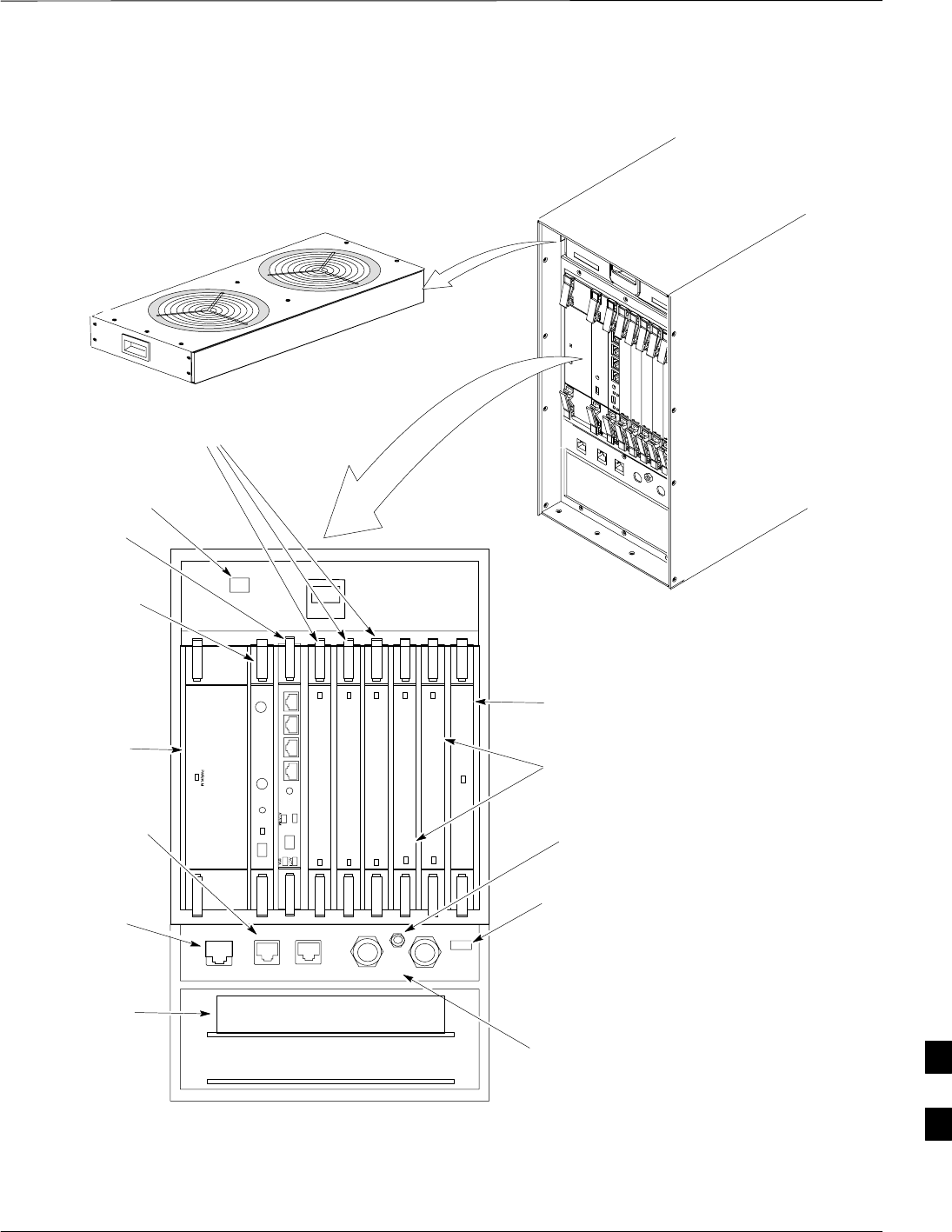
Introduction – continued
Jun 2004 1X SC480 BTS Hardware Installation, Optimization/ATP, and FRU 9-3
DRAFT
Figure 9-2: Compact BTS Fan and CCP2 Shelf Layout
19MHz EVEN RESET ALARM MMI
PWR/ALM
PWR/ALM
PWR/ALM
PWR/ALM
PWR/ALM
PWR/ALM
RESET
GLI
ACTIVE
ACTIVE
ACTIVE
ACTIVE
ACTIVE
BPR A BPR B AUX
MMI
MMI
MCC
cMPC
BBX
GLI
CSA
PS1
LAN A & B
Connections
MCC–DO
Ethernet
Connections
NOTE:
1. HSO or MSO modules
are optional hardware
HSO or MSO
(Note 1)
LED
System
Status
Indicator
GROUP 1 SPAN
DUAL SINGLE LAN A LAN B
ESD
Connector
SPARE
SYSTEM
STATUS
Spare
9
Fan Module
9-4 1X SC480 BTS Hardware Installation, Optimization/ATP, and FRU Jun 2004
DRAFT
Introduction
The fan module is located above the CCP2 Shelf at the front of the
Compact BTS.
The fan mdoule is a modular device allowing easy replacement. The
electrical connection for DC power is made through a connector at the
rear of the module. The connector is automatically engaged when the fan
module is inserted and seated.
System Impact/Considerations
At room temperature, the fan module is very quiet.
Operation can be verified by holding a hand over the
exhaust grill on top and feeling for air movement.
NOTE
Performing this replacement procedure will not cause
downtime or interrupt call processing, but it will trigger
alarms.
IMPORTANT
*
If a fan begins to degrade or fails, an alarm signal will be sent to the
Clock Synchronization Alarms card in the CCP2 Shelf.
Required Items
Documents
None.
Tools
None.
Replacement Units
One fan module (STLN6210)
Prerequisite
Coordinate this repair task with the OMC–R operator.
IMPORTANT
*
Contact the OMC–R operator before performing the replacement
procedure. Tell the operator that the fan module will be replaced and that
alarms can be expected.
9
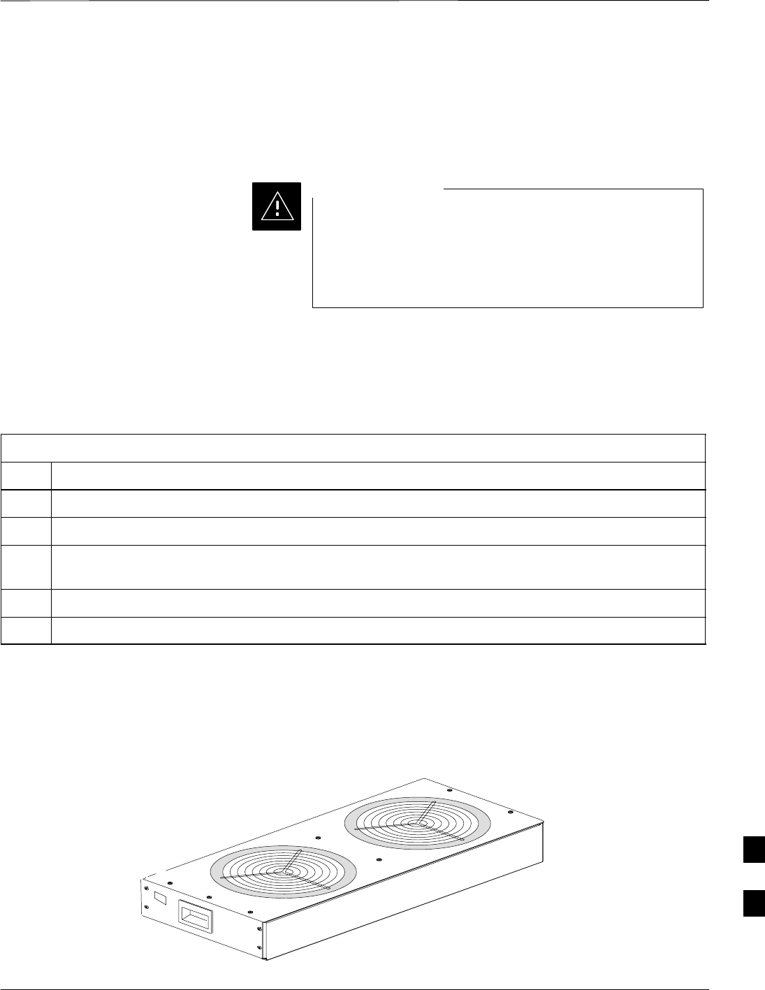
Fan Module – continued
Jun 2004 1X SC480 BTS Hardware Installation, Optimization/ATP, and FRU 9-5
DRAFT
Upon completion of the replacement procedure, have the OMC–R
operator verify that old alarms are cleared and that no new ones are
reported.
Replacement Procedure
This procedure requires working around circuitry that is
extremely sensitive to Electrostatic Discharge (ESD). Wear
a conductive, high impedance wrist strap during the
procedure.
Use appropriate safety measures.
CAUTION
If desired, record the BTS and Fan Module serial number of the failed
unit in Table 9-53 at the end of this chapter.
Remove Fan Module
Use the procedure in Table 9-1 to remove the fan module.
Table 9-1: Procedure to Remove Fan Module
Step Action
1Notify operator that the fan replacement procedure is starting and that alarms can be expected.
2Put on the ESD wrist strap or another approved grounding device.
3If not already done, remove BTS front panel cover by grasping finger grooves at the top and bottom
and pulling simultaneously.
4Lower the latch on front of the fan module while gently pulling it forward.
5When the fan module is half–way out, support it with the other hand and remove it the rest of the way.
Figure 9-3: Fan Module
9

Fan Module – continued
9-6 1X SC480 BTS Hardware Installation, Optimization/ATP, and FRU Jun 2004
DRAFT
Install Fan Module
Use the procedure in Table 9-2 to install the fan module.
Table 9-2: Procedure to Install Fan Module
Step Action
1Put on the ESD wrist strap or another approved grounding device.
2Using both hands, set the fan module in the guide channels, and slide module in.
3Ensure that fan module seats and front latch engages.
4Notify operator that the fan replacement procedure is completed. Have operator verify that old alarms
have cleared and no new alarms are reported.
5Install BTS front panel cover by setting it in place and pushing on the top and bottom simultaneously.
9

High and Medium Stability Oscillator Module
Jun 2004 1X SC480 BTS Hardware Installation, Optimization/ATP, and FRU 9-7
DRAFT
Introduction
The High Stability and Medium Stability Oscillator module provide a
backup reference source in the case of Global Positioning System (GPS)
failure. The HSO is capable of providing up to 24 hours, the
synchronization initially established by the GPS reference signal. The
MSO is capable of providing up to 8 hours.
There is only one HSO or MSO equipped in the Compact BTS. The
module is located in front, behind a cover, underneath the CCP2 Shelf.
The HSO or MSO slides into the top slot of the two that are present.
System Impact/Considerations
The HSO or MSO produces a 1 pulse per second (1 pps) clock output
signal to the CSA.
Front Panel Indicator
The HSO or MSO have no indicators.
Required Items
Documents
None.
Tools
None.
Replacement Units
SOne HSO module (SGLA4007)
SOne MSO module (SGLA4008)
Prerequisite
Coordinate this replacement with the OMC–R operator.
IMPORTANT
*
Contact the OMC–R operator before performing the replacement
procedure. Tell the operator that the HSO or MSO module will be
replaced and that alarms can be expected.
Upon completion of the replacement procedure, have the OMC–R
operator verify that old alarms are cleared and that no new ones are
reported.
9
High and Medium Stability Oscillator Module – continued
9-8 1X SC480 BTS Hardware Installation, Optimization/ATP, and FRU Jun 2004
DRAFT
Replacement Procedure
This procedure requires working around circuitry that is
extremely sensitive to Electrostatic Discharge (ESD). Wear
a conductive, high impedance wrist strap during the
procedure.
Use appropriate safety measures.
CAUTION
If desired, record the BTS and HSO/MSO serial number of the failed
unit in Table 9-54 at the end of this chapter.
Remove HSO or MSO Module
Follow the procedure in Table 9-3 to remove the HSO or MSO module.
See Figure 9-4.
Table 9-3: Procedure to Remove HSO or MSO Module
Step Action
1Notify operator that the HSO or MSO replacement procedure is starting and that alarms can be
expected.
2Put on an ESD wrist strap or other approved grounding device.
3If not already done, remove BTS front panel cover by grasping finger grooves at the top and bottom
and pulling simultaneously.
4If not already done, remove HSO Module cover panel by turning latch, gently pulling it open, and
sliding it out towards the right. The panel has a flange that fits into a slot in the frame.
5Use a T20 star bit to remove two M4 screws securing HSO or MSO to frame.
6Pull on handle to gently slide HSO or MSO out and disconnect cable from side. See Figure 9-5.
Install HSO or MSO
Follow the procedure in Table 9-4 to install the HSO or MSO module.
Table 9-4: Procedure to Install HSO or MSO Module
Step Action
1Put on an ESD wrist strap or other approved grounding device.
* IMPORTANT
The HSO and MSO will only fit into the top slot. DO NOT force it into the lower slot.
2Connect cable to rear of HSO or MSO and slide into top slot.
3Secure HSO or MSO to frame using two M4 screws. Torque screws to 2.3 N–M (20 in–lbs).
table continued on next page
9
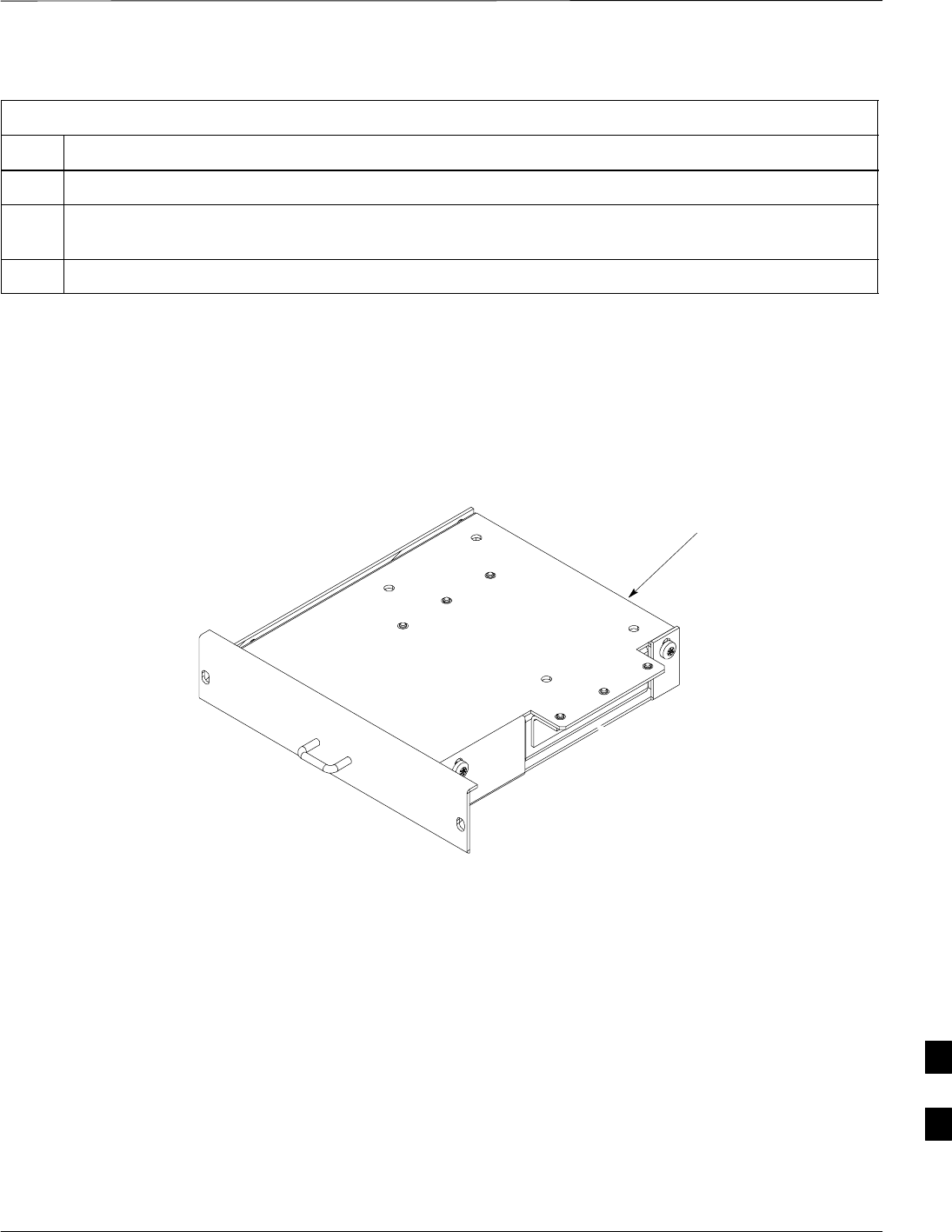
High and Medium Stability Oscillator Module – continued
Jun 2004 1X SC480 BTS Hardware Installation, Optimization/ATP, and FRU 9-9
DRAFT
Table 9-4: Procedure to Install HSO or MSO Module
Step Action
4Install HSO Module cover panel by sliding its flange into the slot, closing, and latching it in place.
5Notify operator that the HSO or MSO replacement procedure is completed. Have operator verify that
old alarms have cleared and no new alarms are reported.
6Install BTS front panel cover by setting it in place and pushing on the top and bottom simultaneously.
Figure 9-4: HSO or MSO Module
Cable connector
9
High and Medium Stability Oscillator Module – continued
9-10 1X SC480 BTS Hardware Installation, Optimization/ATP, and FRU Jun 2004
DRAFT
ti–cdma–wp–00286–v01–ildoc–ah
HSO or MSO
Figure 9-5: HSO or MSO Location
9
Global Positioning System (GPS) Receivers
Jun 2004 1X SC480 BTS Hardware Installation, Optimization/ATP, and FRU 9-11
DRAFT
Introduction
The Compact BTS is configured with either Remote or RF Global
Positioning System (GPS) receiver operation.
For Remote GPS operation, the GPS receiver is located in a
remotely–located GPS head. This head contains a GPS antenna, GPS
receiver, and digital interface. The GPS receiver output signal from the
RGPS head is applied to the Compact BTS. The received signal is routed
to the CSA card.
System Impact/Considerations
If the GPS head has failed, performing the replacement
procedure will not cause an downtime or interrupt call
processing as long as an HSO or MSO has been installed.
If the HSO or MSO has not been “trained” by the GPS for
a minimum of 24 hours, BTS synchronization may not be
maintained for the minimum 24 hours when using the HSO
or 8 hours when using the MSO backup.
IMPORTANT
*
Required Items
Documents
Optimization chapter this manual.
Tools
Appropriate size socket for loosening the pipe/conduit mounting
hardware.
Replacement Unit
One RGPS head (Motorola P/N 0186012H04)
Prerequisite
Coordinate this repair task with the OMC–R operator.
IMPORTANT
*
Replacement Procedure
If desired, record the BTS and RGPS head serial number of the failed
unit in Table 9-55 at the end of this chapter.
Remove RGPS Head
Follow the procedure in Table 9-5 to remove the RGPS Head.
9

Global Positioning System (GPS) Receivers – continued
9-12 1X SC480 BTS Hardware Installation, Optimization/ATP, and FRU Jun 2004
DRAFT
Table 9-5: Procedure to Remove RGPS Head
Step Action
1Notify operator that the RGPS Head replacement procedure is starting and that alarms can be
expected.
2Have the OMC–R operator verify the reference source configuration for the CSA.
* IMPORTANT
Before removing an RGPS Head that has a working RGPS receiver, have the OMC–R operator verify
that the reference source for the CSA is configured for an HSO or MSO.
3Create slack in the RGPS cable so that 0.70 m (2 ft.) of cable extend out of the RGPS Head end of the
mounting pipe/conduit.
NOTE
To prevent twisting of cables, do not unscrew or screw RGPS Head while holding the pipe/conduit.
4Loosen the pipe/conduit mounting hardware until the pipe/conduit is free to be unscrewed from the
RGPS Head.
5Grasp the RGPS Head in one hand and the pipe/conduit in the other.
Unscrew the pipe/conduit from the head and separate.
Grasp the cable just below the head and pull out about 0.5 m (16–inches) of cable out of the
pipe/conduit until the mating cable connectors are exposed.
NOTE
The CSA will automatically switch over to the HSO or MSO approximately 2 seconds after
disconnecting a working RGPS Head. Alarms will be triggered at this time.
Install RGPS Head
Follow the procedure in Table 9-6 to install the RGPS Head.
Table 9-6: Procedure to Install RGPS Head
Step Action
1Connect the cable connector of the replacement RGPS head to the RGPS cable connector.
2Feed the cable slack into the RGPS head end of the mounting pipe/conduit.
3Grasp the RGPS head in one hand and the pipe/conduit in the other.
Being careful not to cross thread the fitting on the RGPS head, screw the pipe/conduit into the head.
Hand tighten only!
4Tighten the pipe/conduit mounting hardware until the pipe/conduit is securely mounted.
5Notify the operator that the replacement procedure has been completed.
Have the operator verify that the original alarms have cleared and that no new alarms are reported.
9
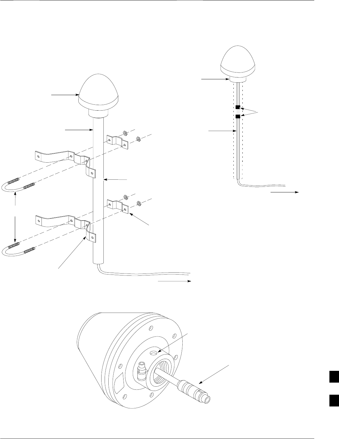
Global Positioning System (GPS) Receivers – continued
Jun 2004 1X SC480 BTS Hardware Installation, Optimization/ATP, and FRU 9-13
DRAFT
WALL MOUNTING
BRACKETS (2)
CLAMP BRACKETS (2)
U–BOLTS
CABLE TO LIGHTNING ARRESTOR
TO SITE I/O INTERFACE (CABLE M)
REFER TO VIEW A FOR
CABLING DETAIL
RGPS HEAD WITH
12 PIN MALE
CONNECTOR
MATING
CONNECTORS
RGPS INTERFACE
CABLE WITH 12 PIN
FEMALE CONNECTOR
ON ONE END AND
UNTERMINATED WIRE
ON OTHER END
VIEW A
RGPS HEAD
(MOTOROLA PART
NUMBER 0186012H03)1
THREADED MOUNT ADAPTER
12–PIN DEUTSCH TYPE MMP
CONNECTOR
RGPS HEAD
CABLE TO LIGHTNING
ARRESTOR TO SITE I/O
INTERFACE (CABLE M)
1–INCH OD
THREADED
CONDUIT
Figure 9-6: RGPS Head and Mounting Pipe/Conduit
NOTE:
1. REPLACEMENT RGPS HEAD
IS MOTOROLA P/N 0186012H04
9
RF–GPS Module
9-14 1X SC480 BTS Hardware Installation, Optimization/ATP, and FRU Jun 2004
DRAFT
Introduction
The procedures in this section cover only the removal and installation of
the RF–GPS Module.
System Impact/Considerations
If the RF–GPS is failing or has failed there will be an interruption in call
processing. The entire site will be down during the replacement of this
component unless an HSO or MSO is in support.
The maximum loss of the RF cable CANNOT exceed
15 dB (assuming 25 dB antenna gain).
IMPORTANT
*
Required Items
Documents
None
Tools
Star screw driver.
Replacement Items
One RF–GPS Receiver (SGRG4030)
One RF–GPS Kit (CGDSGPSKITF4NM50)
Prerequisite
Coordinate this repair task with the OMC–R operator.
IMPORTANT
*
Contact the OMC–R operator before performing the replacement
procedure. Tell the operator that the RF–GPS module will be replaced
and that alarms can be expected.
Upon completion of the replacement procedure, have the OMC–R
operator verify that old alarms are cleared and that no new ones are
reported.
Replacement Procedure
If desired, record the BTS and RF–GPS serial number of the failed unit
in Table 9-56 at the end of this chapter.
Remove RF–GPS
Follow the procedure in Table 9-7 to remove the RF–GPS.
9

RF–GPS Module – continued
Jun 2004 1X SC480 BTS Hardware Installation, Optimization/ATP, and FRU 9-15
DRAFT
Table 9-7: Procedure to Remove RF–GPS
Step Action
1Notify operator that the RF–GPS module replacement procedure is starting and that alarms can be
expected.
2Put on an ESD wrist strap or other approved grounding device.
3At the rear of the BTS, disconnect RF–GPS cable from its SMA connector. See Figure 9-7.
4Using a T20 bit, remove four M4 screws securing RF–GPS module to the CBIO Board.
5Gently remove RF–GPS module (disconnects it from the RGPS D–connector in the CBIO Board) and
place in/on an anti–static container or surface.
Install RF–GPS
Follow the procedure in Table 9-8 to install the RF–GPS.
Table 9-8: Procedure to Install RF–GPS
Step Action
1Put on an ESD wrist strap or other approved grounding device.
2If not already done, remove new RF–GPS module from its anti–static container
3Remove protective cover from RGPS D–connector.
4Install RF–GPS module onto the CBIO Board, by aligning D–connector on bottom of RF–GPS
module with RGPS D–connector on CBIO Board and gently push down on module. See Figure 9-8.
5Using a T20 bit, secure module to CBIO Board with four M4 screws. Torque screws to 2.3 N–M (20
in–lbs).
6Connect RF–GPS cable to the SMA connector. Torque to 1 N–M (9 in–lbs).
7Notify the operator that the replacement procedure is complete.
9
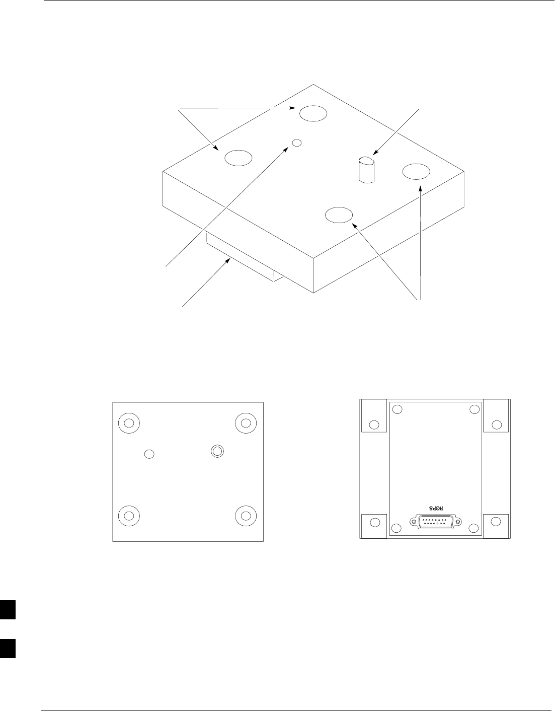
RF–GPS Module – continued
9-16 1X SC480 BTS Hardware Installation, Optimization/ATP, and FRU Jun 2004
DRAFT
Figure 9-7: RF–GPS Module
RF–GPS IN
PWR
RFGPS SERIAL NO.
RFGPS KIT NO.
TOP VIEW BOTTOM VIEW
SMA
Connector
Screw Holes
Screw Holes
Indicator
RGPS
Connector
9
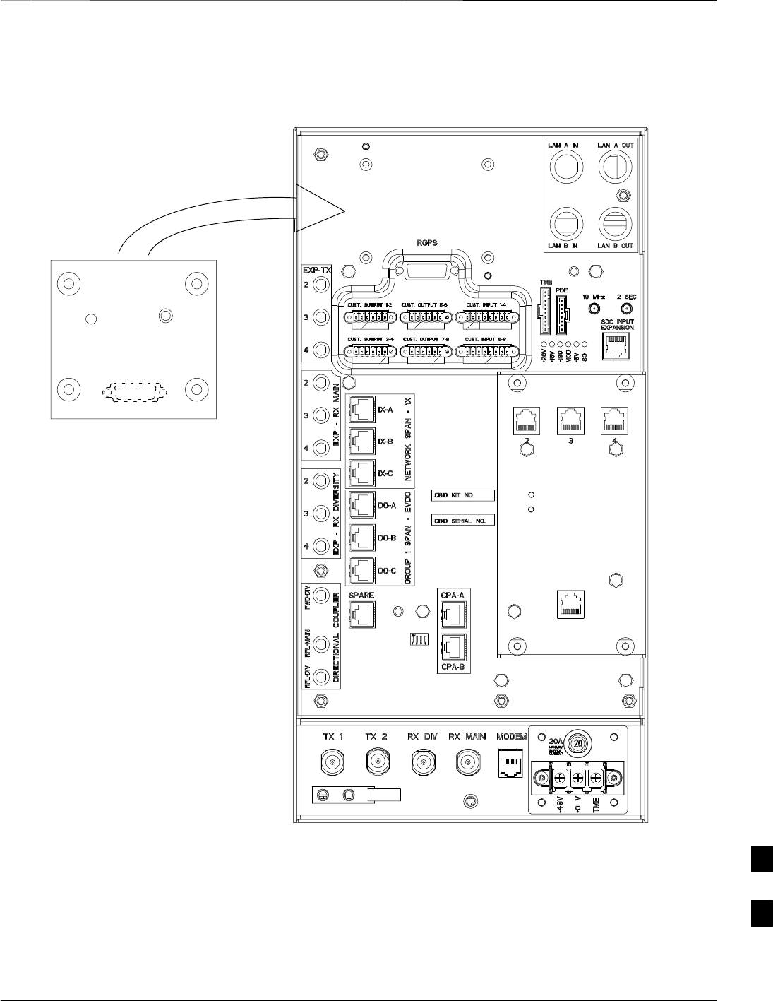
RF–GPS Module – continued
Jun 2004 1X SC480 BTS Hardware Installation, Optimization/ATP, and FRU 9-17
DRAFT
Figure 9-8: RF–GPS Placement on CBIO Board
RF–GPS plugged
in and secured
with four screws.
RF–GPS IN
PWR
RFGPS SERIAL NO.
RFGPS KIT NO.
ti–cdma–wp–00311–v01–ildoc–ah
EXPANSION FRAME SYNC – OUT
DAISY–CHAIN SYNC – OUT
DAISY–CHAIN POWER
SDCX POWER
SDCX KIT NO.
SDCX SERIAL NO.
9
Power Supply Module (PSM)
9-18 1X SC480 BTS Hardware Installation, Optimization/ATP, and FRU Jun 2004
DRAFT
Introduction
The procedures in this section cover only the Power Supply Module
(PSM). The PSM occupies the first slot in the CCP2 Shelf.
System Impact/Consideration
The PSM supplies DC power to the cards/modules of the CCP2 Shelf. If
the module needed replacing it will cause an interruption in call
processing.
Required Items
Documents
None.
Tools
None.
Replacement Unit
One Power Supply Module (STPN4009)
The connector keying for the PSM is different for each
version to prevent using the wrong module.
NOTE
Prerequisite
Coordinate this repair task with the OMC–R operator.
IMPORTANT
*
Contact the OMC–R operator before performing the replacement
procedure. Tell the operator that the PSM will be replaced and that
alarms can be expected.
Upon completion of the replacement procedure, have the OMC–R
operator verify that old alarms are cleared and that no new ones are
reported.
When this module is removed, the BTS will shut down
because power to CCP2 Shelf will be interrupted. It is
recommended that replacing the PSM be performed during
a maintenance window.
IMPORTANT
*
9
Power Supply Module (PSM) – continued
Jun 2004 1X SC480 BTS Hardware Installation, Optimization/ATP, and FRU 9-19
DRAFT
Replacement Procedure
This procedure requires working around circuitry that is
extremely sensitive to Electrostatic Discharge (ESD). Wear
a conductive, high impedance wrist strap during the
procedure.
Use appropriate safety measures.
CAUTION
If desired, record the BTS and PSM serial number of the failed unit in
Table 9-57 at the end of this chapter.
Remove Power Supply Module
Follow the procedure in Table 9-9 to remove the Power Supply Module.
Table 9-9: Procedure to Remove Power Supply Module
Step Action
n WARNING
Disengaging the PSM from the CCP2 Shelf will cause the site to be shutdown due to the disruption in
power to the shelf.
1Notify operator that the PSM replacement procedure is starting and that alarms can be expected.
2At the front of the BTS, remove the front panel cover by grasping finger grooves at the top and
bottom and pulling simultaneously.
3Put on an ESD wrist strap or other approved grounding device.
4Simultaneously press the locking tabs on both the top and bottom module latches
5Pull the latches out to disengage the module from the shelf and slide the card out.
6Place PSM in/on an anti–static container or surface.
Install Power Supply Module
Follow the procedure in Table 9-10 to install the Power Supply Module.
Table 9-10: Procedure to Install Power Supply Module
Step Action
1Put on an ESD wrist strap or other approved grounding device.
2If not already done, remove new PSM from its anti–static container.
3Insert module and carefully slide into slot and push in until it is seated in the backplane.
4Simultaneously pull both latches forward and slip the tips behind the frame.
table continued on next page
9
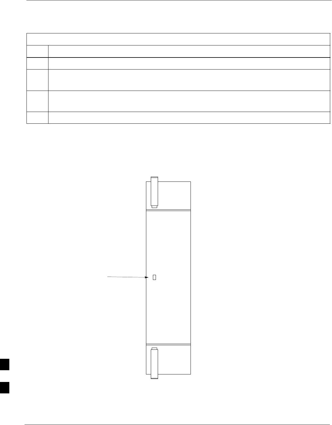
Power Supply Module (PSM) – continued
9-20 1X SC480 BTS Hardware Installation, Optimization/ATP, and FRU Jun 2004
DRAFT
Table 9-10: Procedure to Install Power Supply Module
Step Action
5Push the latches in to engage the module with the backplane and lock the tabs.
6Note that the LED turns red briefly, then green.
Green indicates that it has passed all self–tests and is functional.
7Notify the operator that the replacement procedure has been completed.
Have the operator verify that the original alarms have cleared and that no new alarms are reported.
8Install BTS front panel cover by setting it in place and pushing on the top and bottom simultaneously.
Figure 9-9: Power Supply Module (PSM)
PWR/ALM
PWR/ALM
9
Clock Synchronization Alarms Card
Jun 2004 1X SC480 BTS Hardware Installation, Optimization/ATP, and FRU 9-21
DRAFT
Introduction
The procedures in this section cover only the Clock Synchronization
Alarms (CSA) card. The CSA occupies the second slot in the CCP2
Shelf.
System Impact/Considerations
This replacement procedure does require some system downtime. Since
there is no redundancy, call processing will be interrupted during the
time of the replacement.
Required Items
Documents
None.
Tools
None
Replacement Item
One CSA card.
Prerequisite
Coordinate this repair task with the OMC–R operator.
IMPORTANT
*
Contact the OMC–R operator before performing the replacement
procedure. Tell the operator that the CSA card will be replaced and that
alarms can be expected.
Upon completion of the replacement procedure, have the OMC–R
operator verify that old alarms are cleared and that no new ones are
reported.
Replacement Procedure
If desired, record the BTS and CSA serial number of the failed unit in
Table 9-58 at the end of this chapter.
Remove CSA Module
Follow the procedure in Table 9-11 to remove the CSA card.
Table 9-11: Procedure to Remove CSA Module
Step Action
n WARNING
Disengaging the CSA from the CCP2 Shelf will cause the site to be shutdown due to the disruption in
clock timing to the other cards and modules in the BTS.
1Notify operator that the CSA card replacement procedure is starting and that alarms can be expected.
table continued on next page
9

Clock Synchronization Alarms Card – continued
9-22 1X SC480 BTS Hardware Installation, Optimization/ATP, and FRU Jun 2004
DRAFT
Table 9-11: Procedure to Remove CSA Module
Step Action
2Put on the ESD wrist strap or other approved grounding device.
3If not already done, remove BTS front panel cover by grasping finger grooves at the top and bottom
and pulling simultaneously.
4Simultaneously press the locking tabs on both the top and bottom card latches
5Pull the latches out to disengage the card from the shelf and slide the card out.
6Place card in/on an anti–static container or surface.
Install CSA Module
Follow the procedure in Table 9-12 to install the CSA card.
Table 9-12: Procedure to Install CSA Module
Step Action
1Put on the ESD wrist strap or other approved grounding device.
2If not already done, remove new CSA card from its anti–static container.
3Insert card and carefully slide into slot and push in until it is seated in the backplane.
4Simultaneously pull both latches forward and slip the tips behind the frame.
5Push the latches in to engage the card with the backplane and lock the tabs.
6The LED illuminates red briefly, then turns green.
Green indicates that the module has passed all self–tests and is functional.
7Notify the OMC–R operator that the replacement procedure has been completed, and that old alarms
are cleared and no new alarms are reported.
8If there are no other actions required, install BTS front panel cover by setting it in place and pushing
on the top and bottom simultaneously.
9
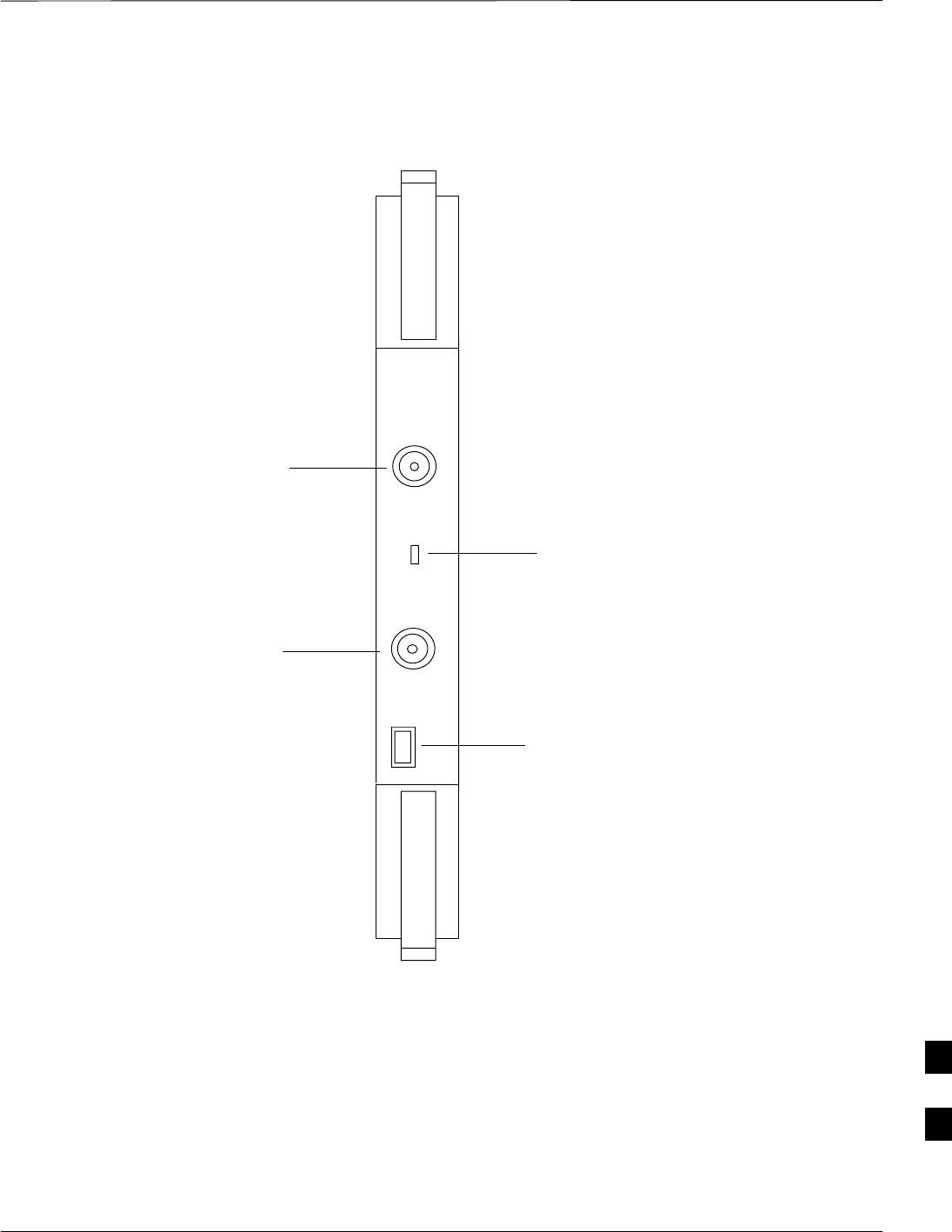
Clock Synchronization Alarms Card – continued
Jun 2004 1X SC480 BTS Hardware Installation, Optimization/ATP, and FRU 9-23
DRAFT
Figure 9-10: Clock Synchronization and Alarm Card
MMI
Frequency Monitor
Synchronization
Monitor
Status/Alarm LED
Man–Machine
Interface
STA/ALM
FREQ. MONITOR
SYNC MONITOR
9
Group Line Interface Card
9-24 1X SC480 BTS Hardware Installation, Optimization/ATP, and FRU Jun 2004
DRAFT
Introduction
The procedures in this section cover only the Group Line Interface
(GLI) 3 card. The GLI3 occupies the third slot in the CCP2 Shelf.
System Impact/Considerations
An interruption in call processing will occur if the GLI3 card is failing
or fails.
Prerequisite
Coordinate this repair task with the OMC–R operator.
IMPORTANT
*
Contact the OMC–R operator before performing the replacement
procedure. Tell the operator that the GLI3 card will be replaced and that
alarms can be expected.
Upon completion of the replacement procedure, have the OMC–R
operator verify that old alarms are cleared and that no new ones are
reported.
When this module is removed, the BTS will shut down
because card interface and communication will be
interrupted. It is recommended that replacing the GLI3 be
performed during a maintenance window.
IMPORTANT
*
Required Items
Documents
This manual for the optimization and acceptance test procedures.
Tools
None
Replacement Item
One GLI3 card (SGLN5975)
Replacement Procedure
This procedure requires working around circuitry that is
extremely sensitive to Electrostatic Discharge (ESD). Wear
a conductive, high impedance wrist strap during the
procedure.
Use appropriate safety measures.
CAUTION
9

Group Line Interface Card – continued
Jun 2004 1X SC480 BTS Hardware Installation, Optimization/ATP, and FRU 9-25
DRAFT
If desired, record the BTS and GLI3 serial number of the failed unit in
Table 9-59 at the end of this chapter.
Remove GLI3 Card
Follow the procedure in Table 9-13 to remove the GLI3 card.
Table 9-13: Procedure to Remove GLI3 Card
Step Action
n WARNING
Disengaging the GLI3 from the CCP2 Shelf will cause the site to be shutdown due to the disruption in
commnuication with the BBX and MCC cards.
1If not already done, remove BTS front panel cover by grasping finger grooves at the top and bottom
and pulling simultaneously.
2Put on the ESD wrist strap or other approved grounding device.
3Notify operator that the GLI3 card replacement procedure is starting and that alarms can be expected.
4Simultaneously press the locking tabs on both the top and bottom card latches
5Pull the latches out to disengage the card from the shelf and slide the card out.
6Place card in/on an anti–static container or surface.
Install GLI3 Card
Follow the procedure in Table 9-14 to install the GLI3 card.
Table 9-14: Procedure to Install GLI3 Card
Step Action
1Put on the ESD wrist strap or other approved grounding device.
2If not already done, remove new GLI3 card from its anti–static container.
3Insert card and carefully slide into slot and push in until it is seated in the backplane.
4Simultaneously pull both latches forward and slip the tips behind the frame.
5Push the latches in to engage the card with the backplane and lock the tabs.
6Check the STATUS and ALARM LEDs:
SThe ALARM LED lights for about 10 seconds while it powers up self–diagnostic test.
SThe STATUS LED lights briefly, indicating that the card has passed self diagnostic tests.
SBoth LEDs should then remain OFF.
table continued on next page
9

Group Line Interface Card – continued
9-26 1X SC480 BTS Hardware Installation, Optimization/ATP, and FRU Jun 2004
DRAFT
Table 9-14: Procedure to Install GLI3 Card
Step Action
NOTE
If the red ALARM LED remains ON, the card may not be fully seated in the backplane. Pull the card
out about halfway, wait about two minutes before reseating. Perform steps 4 and 5.
If the red LED turns back ON after the green LED turns OFF, a new failure condition exists and an
alarm generated.
7Notify operator that the GLI3 replacement procedure is completed. Have operator verify that old
alarms have cleared and no new alarms are reported.
8Using the LMF connected to the MMI port, verify that new GLI3 card has the proper configuration.
9Proceed to Table 9-15.
GLI3 Recovery Procedure
Follow the procedure in Table 9-15 to recover the GLI3 card.
Table 9-15: Procedure to Recover GLI3 Card
Step Action
1At the prompt, enter the following command:
omc–00000>ENABLE GLI–<bts#>–<gli#> UNC
2Display the status of the GLI by entering the following command:
omc–00000>DISPLAY BTS–<bts#> STATUS
3Verify the status of the new GLI3 is INS_ACTIVE.
4If there are no other actions required, install BTS front panel cover by setting it in place and pushing
on the top and bottom simultaneously.
Optimization Requirement
Refer to the Optimization section of this manual and perform the
required procedures.
9
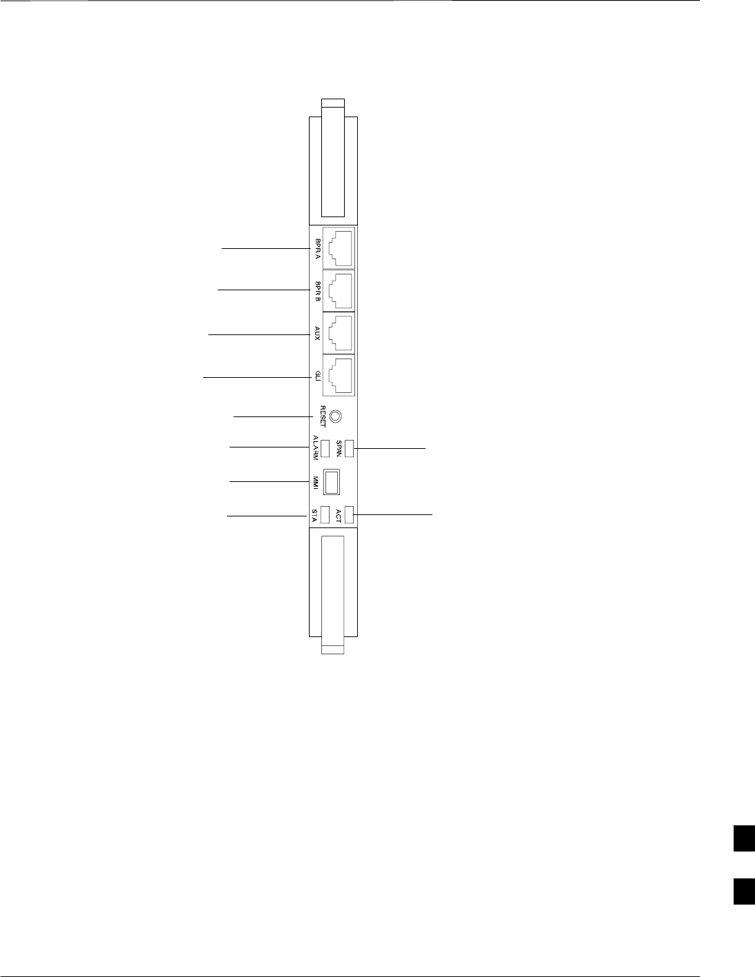
Group Line Interface Card – continued
Jun 2004 1X SC480 BTS Hardware Installation, Optimization/ATP, and FRU 9-27
DRAFT
Figure 9-11: Group Line Interface 3 Card
BPR A
BPR B
AUX
GLI
RESET
ALARM
MMI
ACT
SPAN
STA
9

Multi–Channel CDMA Card
9-28 1X SC480 BTS Hardware Installation, Optimization/ATP, and FRU Jun 2004
DRAFT
Introduction
The procedures in this section cover only the Multi–Channel CDMA
(MCC) cards. The MCC–1X cards occupy the fourth, fifth, and sixth
slots (MCC 1, 2, & 3) in the CCP2 Shelf.
If the MCC–DO card is in use, proceed to that section for more
information later in this chapter.
System Impact/Considerations
If an MCC–1X card fails it will cause some interruption in call
processing in the sense that not all calls will be handled. The other
MCC–1X cards may not be able to handle the additional calls thus calls
on the failing or failed card will be dropped.
If an MCC–1X card must be replaced, it must be ensured that it has the
same number of channels as the card being replaced.
MCC Front Panel
PWR/ALM LED
The MCC–1X card has its own alarm (fault) detection circuitry that
controls the state of the PWR/ALM LED. When the LED is:
SGreen –
– OFF – INS_ACT no alarm.
SRed – Power-up or fault condition.
Active LED
The MCC–1X card has circuitry that controls the state of the Active
LED. When the LED is:
SGreen –
– Solid – INS_ACT no alarm.
– Rapidly Flashing – OOS_RAM no alarm.
– Slowly Flashing – OOS_ROM no alarm.
SRed –
– Fault condition or card is in reset.
– Slow flashing (alternating with green) – CHI bus inactive on power
up.
Required Items
Documents
None.
Tools
None.
9
Multi–Channel CDMA Card – continued
Jun 2004 1X SC480 BTS Hardware Installation, Optimization/ATP, and FRU 9-29
DRAFT
Replacement Items
SUp to 3 MCC–1X–16 cards (SGLN6117)
SUp to 3 MCC–1X–32 cards (SGLN6050)
SUp to 3 MCC–1X–48 cards (SGLN6051)
SUp to 3 MCC–1X–64 cards (SGLN6052) (for Packet Backhaul)
Prerequisite
Coordinate this repair task with the OMC–R operator.
IMPORTANT
*
Contact the OMC–R operator before performing the replacement
procedure. Tell the operator that the MCC–1X card will be replaced and
that alarms can be expected.
Upon completion of the replacement procedure, have the OMC–R
operator verify that old alarms are cleared and that no new ones are
reported.
Replacement Procedure
This procedure requires working around circuitry that is
extremely sensitive to Electrostatic Discharge (ESD). Wear
a conductive, high impedance wrist strap during the
procedure.
Use appropriate safety measures.
CAUTION
If desired, record the BTS and MCC serial number of the failed unit in
Table 9-60 at the end of this chapter.
Remove MCC–1X Card
Follow the procedure in Table 9-16 to remove the MCC–1X card.
Table 9-16: Procedure to Remove MCC–1X Card
Step Action
n WARNING
Due to a lack of redundancy, disengaging the MCC cards from the CCP2 Shelf will cause the site to be
shutdown due to the disruption in communication with the GLI3.
1Notify operator that the MCC replacement procedure is starting and that alarms can be expected.
2Put on the ESD wrist strap or other approved grounding device.
3If not already done, remove BTS front panel cover by grasping finger grooves at the top and bottom
and pulling simultaneously.
table continued on next page
9

Multi–Channel CDMA Card – continued
9-30 1X SC480 BTS Hardware Installation, Optimization/ATP, and FRU Jun 2004
DRAFT
Table 9-16: Procedure to Remove MCC–1X Card
Step Action
4Simultaneously press the locking tabs on both the top and bottom card latches
5Pull the latches out to disengage the card from the shelf and slide the card out.
6Place MCC–1X card on/in an anti–static container or surface.
Install MCC–1X Card
Follow the procedure in Table 9-17 to install the MCC–1X card.
Table 9-17: Procedure to Install MCC–1X Card
Step Action
1Put on the ESD wrist strap or other approved grounding device.
2If not already done, remove new MCC–1X card from anti–static container.
3Slide card into slot and simultaneously pull both latches forward and slip the tips behind the frame.
4Push the latches in to engage the card with the backplane and lock the tabs.
5Notify operator that the MCC replacement procedure is completed. Have operator verify that old
alarms have cleared and no new alarms are reported.
6If there are no other actions required, install BTS front panel cover by setting it in place and pushing
on the top and bottom simultaneously.
Optimization Requirement
Refer to the Optimization section of this manual and perform the
required procedures.
9

Multi–Channel CDMA Card – continued
Jun 2004 1X SC480 BTS Hardware Installation, Optimization/ATP, and FRU 9-31
DRAFT
Figure 9-12: MCC 1X Card
PWR/ALM ACTIVE
Power/Alarm LED
Active LED
9

Broadband Transceiver Card
9-32 1X SC480 BTS Hardware Installation, Optimization/ATP, and FRU Jun 2004
DRAFT
Introduction
The procedures in this section cover only the Broad Band Transceiver
1X (BBX–1X) cards. These cards occupy the seventh and eighth slots
(BBX 1 & 4) of the CCP2 Shelf.
System Impact/ Considerations
The Compact BTS is not configured for redundancy, so a failure of the
BBX card will cause an interruption in call processing. It is still
“hot–swappable” like its Macrocell counterparts. Once replacement is
made, optimization procedures will have to be performed.
Front Panel
The BBX–1X card contains the PWR/ALM and ACTIVE LED’s, reset
switch and MMI port connector. A removable lens covers these items
and deters access to the reset switch and MMI port. Refer to Figure 9-13.
PWR/ALM LED
The BBX module has its own alarm (fault) detection circuitry that
controls the state of the PWR/ALM LED. When the LED is:
SGreen –
– Solid – INS_ACT no alarm.
– Slowly Flashing – OOS_ROM no alarm.
– Rapidly Flashing – OOS_RAM no alarm.
SRed – initializing or power-up or alarm condition.
SCombinations
– Long red/Short green– OOS_ROM alarm.
– Short red/Short green – OOS_RAM alarm.
– Long green/Short red – INS_ACT alarm.
SOFF
– No DC power
– The on–board fuse is open.
Active LED
The BBX module has circuitry that controls the state of the Active LED.
When the LED is:
SGreen – Operating in INS_ACTIVE state and keyed. No alarm
condition present.
SRed –
– Color during initial system power–up.
– Operating in FAULT (alarm) state. Alarm condition is present.
9
Broadband Transceiver Card – continued
Jun 2004 1X SC480 BTS Hardware Installation, Optimization/ATP, and FRU 9-33
DRAFT
Required items
Documents
This manual for optimization and acceptance test procedures.
Tools
None
Replacement Unit
SBBX–1X card (SGLG4044)
Prerequisite
Coordinate this repair task with the OMC–R operator.
IMPORTANT
*
Contact the OMC–R operator before performing the replacement
procedure. Tell the operator that the BBX–1X card will be replaced and
that alarms can be expected.
Upon completion of the replacement procedure, have the OMC–R
operator verify that old alarms are cleared and that no new ones are
reported.
Replacement Procedure
This procedure requires working around circuitry that is
extremely sensitive to Electrostatic Discharge (ESD). Wear
a conductive, high impedance wrist strap during the
procedure.
Use appropriate safety measures.
CAUTION
If desired, record the BTS and BBX–1X serial number of the failed unit
in Table 9-61 at the end of this chapter. BBX 1 and 4 will be present if
BTS is configured for two carriers; otherwise, only BBX 1 will be
present.
9

Broadband Transceiver Card – continued
9-34 1X SC480 BTS Hardware Installation, Optimization/ATP, and FRU Jun 2004
DRAFT
Remove BBX–1X Card
Follow the procedure in Table 9-18 to remove the BBX–1X card.
Table 9-18: Procedure to Remove BBX–1X Card
Step Action
n WARNING
Due to a lack of redundancy, disengaging the BBX card(s) from the CCP2 Shelf will cause the site to
be shutdown due to the disruption in communication with the GLI3 and loss of carrier.
1Notify operator that the BBX–1X card replacement procedure is starting and that alarms can be
expected.
2Put on the ESD wrist strap or other approved grounding device.
3If not already done, remove BTS front panel cover by grasping finger grooves at the top and bottom
and pulling simultaneously.
4Simultaneously press the locking tabs on both the top and bottom card latches
5Pull the latches out to disengage the card from the shelf and slide the card out.
6Place on/in an anti–static container or surface.
Install BBX–1X Card
Follow the procedure in Table 9-19 to install the BBX–1X card.
Table 9-19: Procedure to Install BBX–1X Card
Step Action
1Put on the ESD wrist strap or other approved grounding device.
2If not already done, remove new BBX–1X card from anti–static container.
3Slide card into slot and simultaneously pull both latches forward and slip the tips behind the frame.
4Push the latches in to engage the card with the backplane and lock the tabs.
5Notify operator that the BBX–1X replacement procedure is completed. Have operator verify that old
alarms have cleared and no new alarms are reported.
6If there are no other actions required, install BTS front panel cover by setting it in place and pushing
on the top and bottom simultaneously.
Optimization Requirement
Refer to the Optimization section of this manual and perform the
required procedures.
9
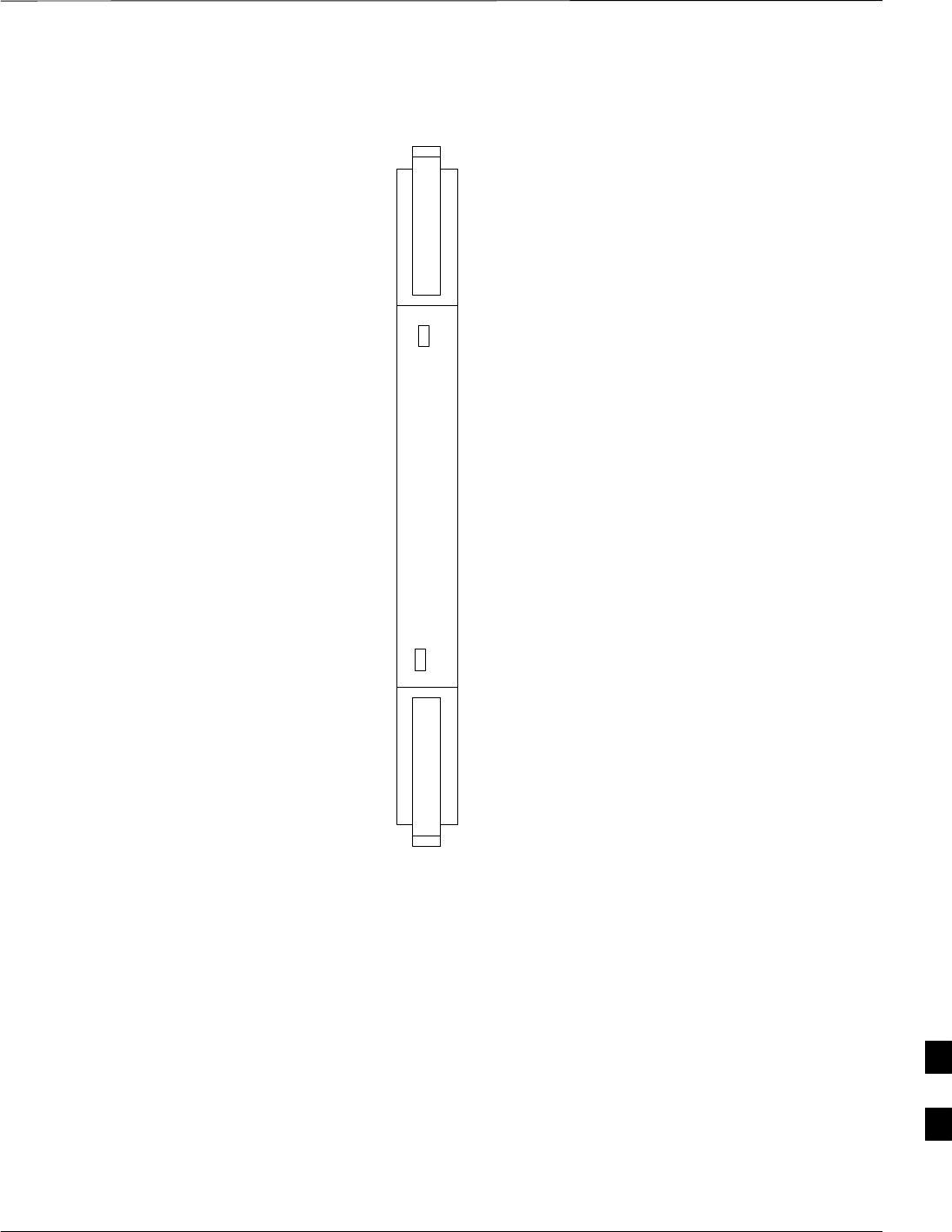
Broadband Transceiver Card – continued
Jun 2004 1X SC480 BTS Hardware Installation, Optimization/ATP, and FRU 9-35
DRAFT
Figure 9-13: BBX–1X Card
PWR/ALM ACTIVE
9

Compact BTS Multi–Coupler Preselector Card
9-36 1X SC480 BTS Hardware Installation, Optimization/ATP, and FRU Jun 2004
DRAFT
Introduction
The procedures in this section cover only the Multi–Coupler Preselector
Card (cMPC). The cMPC occupies the ninth slot of the CCP2 Shelf.
cMPC PWR/ALM LED States
The cMPC has a dual color (green & red) power/alarm (PWR/ALM)
status indicator LED located on its front panel. The card has its own
alarm (fault) detection circuitry that controls what is displayed on the
LED. Table 9-20 lists these states. Refer to Figure 9-14.
Table 9-20: cMPC PWR/ALM LED State
LED State Device State
Steady GREEN Operating normally
Steady RED 1. Displayed during initial
power– up.
2. Operating in a Fault condition.
OFF No DC power to card.
System Impact/Considerations
An interruption in call processing, due to the RX signal path being
broken, will occur if the cMPC must be replaced due to total failure or
marginal operation.
Required items
Documents
This manual for optimization and acceptance test procedures.
Tools
None
Replacement Unit
ScMPC (STLF4110)
Prerequisite
Coordinate this repair task with the OMC–R operator.
IMPORTANT
*
Contact the OMC–R operator before performing the replacement
procedure. Tell the operator that the Compact MPC will be replaced and
that alarms can be expected.
9

Compact BTS Multi–Coupler Preselector Card – continued
Jun 2004 1X SC480 BTS Hardware Installation, Optimization/ATP, and FRU 9-37
DRAFT
Upon completion of the replacement procedure, have the OMC–R
operator verify that old alarms are cleared and that no new ones are
reported.
Replacement Procedure
This procedure requires working around circuitry that is
extremely sensitive to Electrostatic Discharge (ESD). Wear
a conductive, high impedance wrist strap during the
procedure.
Use appropriate safety measures.
CAUTION
Before Beginning
If desired, record the BTS and cMPC serial number of the failed unit in
Table 9-62 at the end of this chapter.
Remove cMPC
Follow the procedure in Table 9-21 to remove the cMPC.
Table 9-21: Procedure to Remove cMPC
Step Action
1Notify operator that the cMPC replacement procedure is starting and that alarms can be expected.
2Put on an ESD wrist strap or other approved grounding device.
3If not already done, remove BTS front panel cover by grasping finger grooves at the top and bottom
and pulling simultaneously.
4Simultaneously press the locking tabs on both the top and bottom card latches
Pull the latches out to disengage the card from the shelf and slide the card out far enough to disconnect
the RF cabling.
* IMPORTANT
If the BTS is set up for 2 PAs, then there will be 6 RF cables (fitted with QMA connectors) to
disconnect.
Recommend that the cables be disconnected either from top–to–bottom or bottom–to–top. This will
be important when re–connecting the cables.
At the rear of the card the jumper will be connected to the upper of the two RF connections
5Cables are labeled and color coded, if not, then tag each cable as it is disconnected.
Once cables are disconnected, pull out card.
6Place in/on an anti–static container or surface.
Install cMPC
Follow the procedure in Table 9-22 to install the cMPC.
9

Compact BTS Multi–Coupler Preselector Card – continued
9-38 1X SC480 BTS Hardware Installation, Optimization/ATP, and FRU Jun 2004
DRAFT
Table 9-22: Procedure to Install cMPC
Step Action
1Put on an ESD wrist strap or other approved grounding device.
2If not already done, remove new cMPC from its anti–static container.
3Verify that the cMPC is set up for using 1 or 2 Compact PAs. See Figure 9-15.
SFor 1 PA, the jumper should be connected to the “Default” RF connector.
SFor 2 PAs, the jumper should be connected to the “Alternate” RF connector.
* IMPORTANT
To insert the cMPC with minimum of trouble, make sure the RF cabling is held away towards the side
of the frame in single file and in order they were disconnected.
4Insert card and carefully slide into slot far enough to attach cables.
Attach RF cables (each cable is labeled and color coded)
5Simultaneously pull both latches forward and slip the tips behind the frame.
6Push the latches in to engage the card with the backplane and lock the tabs.
7Note that the LED turns red briefly, then green.
Green indicates that it has passed all self–tests and is functional.
8Notify operator that the cMPC replacement procedure is completed. Have operator verify that old
alarms have cleared and no new alarms are reported.
9If no other action is needed, install BTS front panel cover by setting it in place and pushing on the top
and bottom simultaneously.
9

Compact BTS Multi–Coupler Preselector Card – continued
Jun 2004 1X SC480 BTS Hardware Installation, Optimization/ATP, and FRU 9-39
DRAFT
Figure 9-14: Compact Multi–Coupler Preselector Card
POWER/ALARM LED
PWR/ALM
9
Compact BTS Multi–Coupler Preselector Card – continued
9-40 1X SC480 BTS Hardware Installation, Optimization/ATP, and FRU Jun 2004
DRAFT
Figure 9-15: Compact Multi–Coupler Preselector Card Jumper Connection
DEFAULT
ALTERNATE
Compact MPC shown is set for 1 Power Amplifier
P/O cMPC
9

MCC Data Only (MCC–DO) Card
Jun 2004 1X SC480 BTS Hardware Installation, Optimization/ATP, and FRU 9-41
DRAFT
Introduction
The procedures in this section cover only the MCC Data Only
(MCC–DO) card. If in use, this card utilizes MCC slots 1 and 2, with
slot 3 containing an MCC–1X card or a filler panel.
EV–DO FRU Information
If there are conflicts between the procedures presented here and the
material presented in 1xEV–DO Field Replaceable Unit (FRU)
Procedures – 68P09257A99, the manual takes precedence.
System Impact/Considerations
If the Multi–Channel CDMA Data Only card fails or is removed from
service, there will be an interruption in call processing.
LED States
The MCC–DO card uses four front panel LEDs to indicate its status.
Table 9-23 lists the states of the MCC–DO LEDs.
Table 9-23: MCC–DO LED States
LED Color Status SPAN
Green ON INS or INS_SBY or INS_ACT
PWR/ALM ON Not installed or OOS.
Red Blinking Installed in wrong slot.
–– OFF Off
Green ON INS_ACT
Blinking OOS or INS_SBY
Red ON Not Initialized.
ACT Blinking Installed in wrong slot.
Orange ON INS
–– OFF Off
Red ON Major alarms on a provisioned span.
SPAN Orange ON Minor alarms on a provisioned span.
Green ON No alarms on a provisioned span.
–– OFF No Provisioned span.
Orange ON Both ENET and TAT links are up.
ENET Green ON Either ENET or TAT link is up.
table continued on next page
9
MCC Data Only (MCC–DO) Card – continued
9-42 1X SC480 BTS Hardware Installation, Optimization/ATP, and FRU Jun 2004
DRAFT
Table 9-23: MCC–DO LED States
LED SPANStatusColor
–– OFF Both ENET and TAT link are down.
NOTE: In the case of some spans on a given MCC–DO having Yellow alarms, and other
spans having Red alarms, a Red Alarm state should be indicated.
Required Items
Documents
None.
Tools
None.
Replacement Items
One MCC–Data Only card (SGLN6146)
Prerequisite
Coordinate this repair task with the OMC–R operator.
IMPORTANT
*
Contact the OMC–R operator before performing the replacement
procedure. Tell the operator that the MCC–DO card will be replaced and
that alarms can be expected.
Upon completion of the replacement procedure, have the OMC–R
operator verify that old alarms are cleared and that no new ones are
reported.
Replacement Procedure
If desired, record the BTS and MCC–DO serial number of the failed unit
in Table 9-63 at the end of this chapter.
Remove MCC–DO Card
Follow the procedure in Table 9-24 to remove the MCC–DO card.
Table 9-24: Procedure to Remove MCC–DO Card
Step Action
n WARNING
Disengaging the MCC–DO card from the CCP2 Shelf will cause the site to be shutdown due to the
disruption in signal processing.
1Notify operator that the MCC–DO card replacement procedure is starting and that alarms can be
expected.
table continued on next page
9

MCC Data Only (MCC–DO) Card – continued
Jun 2004 1X SC480 BTS Hardware Installation, Optimization/ATP, and FRU 9-43
DRAFT
Table 9-24: Procedure to Remove MCC–DO Card
Step Action
2Put on the ESD wrist strap or other approved grounding device.
3If not already done, remove BTS front panel cover by grasping finger grooves at the top and bottom
and pulling simultaneously.
4If not already done, label cables prior to disconnecting them from front panel connectors.
5Simultaneously press the locking tabs on both the top and bottom card latches
6Pull the latches out to disengage the card from the shelf and slide the card out.
7Place in/on an anti–static container or surface.
Install MCC–DO Card
Follow the procedure in Table 9-25 to install the MCC–DO card.
Table 9-25: Procedure to Install MCC–DO Card
Step Action
1Put on the ESD wrist strap or other approved grounding device.
2If not already done, remove new MCC–DO card from anti–static container.
3Slide card into slot and simultaneously pull both latches forward and slip the tips behind the frame.
4Push the latches in to engage the card with the backplane and lock the tabs.
5Note that the PWR/ALM LED turns red briefly, then green.
Green indicates that it has passed all self–tests and is functional.
6Connect cabling to front panel connectors.
7Notify operator that the MCC–DO replacement procedure is completed. Have operator verify that old
alarms have cleared and no new alarms are reported.
8If there are no other actions required, install BTS front panel cover by setting it in place and pushing
on the top and bottom simultaneously.
9
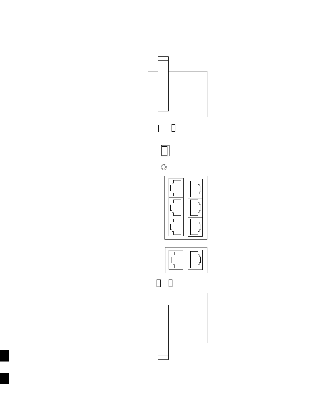
MCC Data Only (MCC–DO) Card – continued
9-44 1X SC480 BTS Hardware Installation, Optimization/ATP, and FRU Jun 2004
DRAFT
Figure 9-16: MCC–DO Card
NOTE:
1. The DO card physically occupies
MCC slots 1 & 2, but only plugs into
one backplane connector
ENET
ACT
MMI ENET
TAT
GRP3
SPAN
GRP2
SPAN
GRP1
SPAN
SINGLE
DUAL
SPAN
PWR/ALM RESET
9

Compact BTS Input and Output Board
Jun 2004 1X SC480 BTS Hardware Installation, Optimization/ATP, and FRU 9-45
DRAFT
Introduction
The procedures in this section cover only the removal and installation of
the Compact BTS Input and Output (CBIO) Board.
System Impact/Considerations
If the CBIO board is failing or has failed there will be an interruption in
call processing. The entire site will be down for replacement of this
component.
CBIO Indicators
The CBIO Board has six indicators that provide status of several
components of the BTS. The six LEDs are +28V, +15V, HSO, MOD,
+5V, and ISO.
+28V LED
The +28V LED indicates the status of the DC power that is supplied to
the Remote GPS or the RF GPS module. This LED will come on after
the CSA initializes. When the CSA is trying to determine the cable
delay, this LED will go OFF and ON, but it should stay ON once the
delay is successfully completed. If the LED remains OFF, it may
indicate a problem with either the RGPS or RF GPS, or the CSA FRU.
+15V LED
The +15V LED indicates the status of the DC power that is coming from
the DC–DC converter module to the CBIO Board. This LED should
always be ON, unless there is a blown fuse on the CBIO Board.
HSO LED
The HSO LED indicates the status of the DC power that is supplied to
the HSO or MSO module. This LED will be OFF, if the HSO or MSO
is not connected; otherwise, it is ON. Faulty operation of the LED may
be related to problems with the main +15V supply to the CBIO Board,
also indicated by the +15V LED.
MOD LED
The MOD LED indicates the status of the DC power that is supplied to
the modem module. However, this LED is not dependent on whether the
modem module is plugged in or not, and should be always ON. If the
CBIO +5V supply is okay, then the LED being OFF could indicate a
problem with the modem module, the wiring, or a resettable fuse on the
CBIO Board.
+5V LED
The +5V LED indicates the status of the DC power that is coming from
the DC–DC converter module to the CBIO Board. This LED should
always be ON, unless there is a blown fuse on the CBIO Board.
9
Compact BTS Input and Output Board – continued
9-46 1X SC480 BTS Hardware Installation, Optimization/ATP, and FRU Jun 2004
DRAFT
ISO LED
The ISO LED indicates the status of the isolated DC voltage that is used
for the customer inputs. This LED should always be ON, if the +5V
supply to the CBIO Board is okay. If the LED is OFF, it indicates a
problem on the CBIO Board.
Required Items
Documents
None
Tools
Screwdriver with T20 star bit
Replacement Items
One CBIO Board.
Prerequisite
Coordinate this repair task with the OMC–R operator.
IMPORTANT
*
Contact the OMC–R operator before performing the replacement
procedure. Tell the operator that the CBIO will be replaced and that
alarms can be expected.
Upon completion of the replacement procedure, have the OMC–R
operator verify that old alarms are cleared and that no new ones are
reported.
Replacement Procedure
If desired, record the BTS and CBIO Board serial number of the failed
unit in Table 9-64 at the end of this chapter.
Remove CBIO Board
Follow the procedure in Table 9-26 to remove the CBIO Board.
To perform the following procedure, the BTS must be
removed from the Mounting Plate.
NOTE
Table 9-26: Procedure to Remove CBIO Board
Step Action
1Notify operator that the CBIO Board replacement procedure is starting and that alarms can be
expected.
2 Perform the Site Shutdown procedure in Table 10-2.
table continued on next page
9

Compact BTS Input and Output Board – continued
Jun 2004 1X SC480 BTS Hardware Installation, Optimization/ATP, and FRU 9-47
DRAFT
Table 9-26: Procedure to Remove CBIO Board
Step Action
n WARNING
By pulling out the circuit breaker, power to the BTS will be interrupted, causing the BTS to go off
line.
3Disengage DC power to the BTS by pulling out the 20 A breaker at the rear of the BTS.
4If possible, turn off DC power at the source. Verify that DC power source is OFF.
5Disconnect all cabling to the BTS.
6Put on the ESD wrist strap.
7At the rear of the BTS, remove the four M4 screws securing the SDCX or SDCX cover plate to the
CBIO Board. Gently remove SDCX module from the CBIO connector or SDCX cover plate.
8Use a driver with a T20 star bit to remove 6 M4 screws securing CBIO to housing. See Figure 9-17.
* IMPORTANT
DO NOT yank out the CBIO Board, there are cables connected at the bottom rear side of the board.
9Grasp holes and gently pull on CBIO Board to disengage it from the backplane. See Figure 9-17.
Note that there are internal cables connected at the bottom.
10 If not already done, label internal cables before disconnecting them.
11 Remove CBIO Board and place in an anti–static container.
Install CBIO Board
Follow the procedure in Table 9-27 toinstall the CBIO Board.
Table 9-27: Procedure to Install CBIO Board
Step Action
1Put on the ESD wrist strap.
2If not already done, remove CBIO Board from its anti–static container.
3Set CBIO Board onto rear of BTS and connect the internal cables, in the same order as previously
connected.
4Carefully align the CBIO panel to the frame and gently seat the CBIO connector into the backplane
connector.
5Once aligned, with one hand grasp BTS and with the other hand gently push the CBIO until it sets up
against the housing.
6Use a driver with a T20 star bit to secure the CBIO to the frame using 6 M4 screws. Torque screws to
2.3 N–M (20 in–lbs). See Figure 9-17.
7Install SDCX or SDCX cover plate and secure to CBIO using 4 M4 screws. Torque screws to 2.3
N–M (20 in–lbs).
table continued on next page
9

Compact BTS Input and Output Board – continued
9-48 1X SC480 BTS Hardware Installation, Optimization/ATP, and FRU Jun 2004
DRAFT
Table 9-27: Procedure to Install CBIO Board
Step Action
8Disengage from the ESD wrist strap.
9Connect all external cabling.
10 Verify that DC power source is OFF before re–connecting to the BTS.
Turn on DC power source.
11 Notify the operator know that the replacement procedure is completed, and that power up will begin
shortly.
12 Allow the BTS to power up by pushing in the 20 A circuit breaker at the rear of the BTS.
13 Perform the Site Startup procedure in Table 10-5.
14 Perform an optimization of the cards, using the procedures in the Optimization/ATP section of this
manual.
15 After BTS is optimized and is operating within normal parameters, install the BTS front cover panel
by setting it in place and pushing on the top and bottom simultaneously.
16 Notify operator that optimization is complete.
9
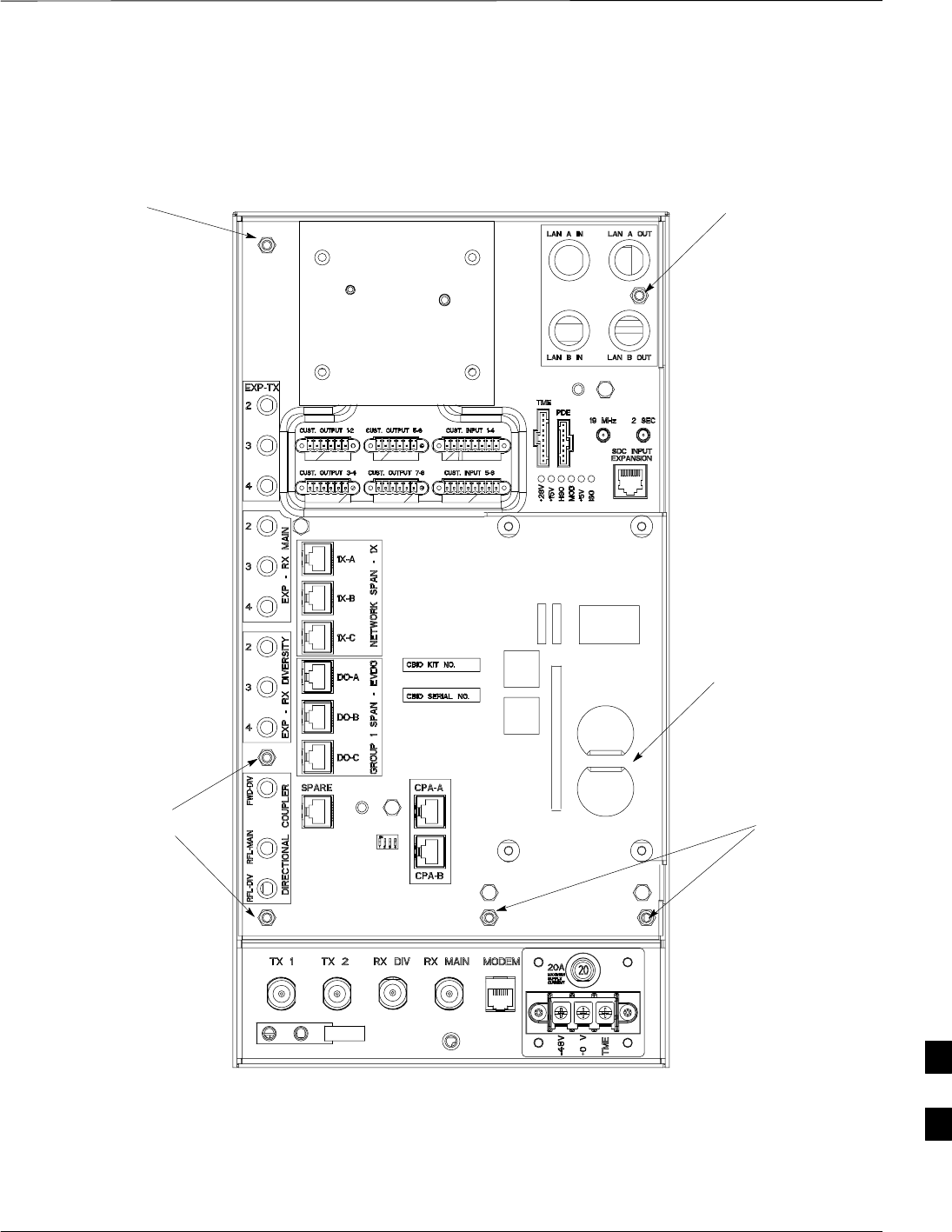
Compact BTS Input and Output Board – continued
Jun 2004 1X SC480 BTS Hardware Installation, Optimization/ATP, and FRU 9-49
DRAFT
Figure 9-17: CBIO Board with SDCX Removed
ti–cdma–wp–00311–v01–ildoc–ah
RF–GPD IN
PWR
Screws to
remove
Screws to
remove
Screw to
remove
Screw to
remove
Grasp holes
with forefinger
and thumb.
SDCX Board or
Cover Plate
Removed
9
SDCX Module
9-50 1X SC480 BTS Hardware Installation, Optimization/ATP, and FRU Jun 2004
DRAFT
Introduction
The procedures in this section cover only the removal and installation of
the Synchronization Daisy–Chaining and eXpansion (SDCX) Module.
System Impact/Considerations
If the SDCX fails it will cause a disruption in call processing by
upsetting the timing of the BTSs.
Required Items
Documents
None
Tools
Star screw driver.
Replacement Items
One SDCX Module (SGLN6153)
Prerequisite
Coordinate this repair task with the OMC–R operator.
IMPORTANT
*
Contact the OMC–R operator before performing the replacement
procedure. Tell the operator that the SDCX module will be replaced and
that alarms can be expected.
Upon completion of the replacement procedure, have the OMC–R
operator verify that old alarms are cleared and that no new ones are
reported.
Replacement Procedure
If desired, record the BTS and SDCX serial number of the failed unit in
Table 9-65 at the end of this chapter.
Remove SDCX
Follow the procedure in Table 9-28 to remove the SDCX Module.
Table 9-28: Procedure to Remove SDCX
Step Action
1Notify operator that the SDCX Module replacement procedure is starting and that alarms can be
expected.
2Put on an ESD wrist strap or other approved grounding device.
table continued on next page
9

SDCX Module – continued
Jun 2004 1X SC480 BTS Hardware Installation, Optimization/ATP, and FRU 9-51
DRAFT
Table 9-28: Procedure to Remove SDCX
Step Action
3Disconnect all cables from SDCX Module.
4At the rear of the BTS, use a T20 screw driver to remove four M4 screws securing SDCX Module to
the CBIO Board. See Figure 9-19.
5Gently remove SDCX Module (disconnect it from the SDCX connector in the CBIO Board), and place
it in/on an anti–static container or surface.
Install SDCX
Follow the procedure in Table 9-29 to install the SDCX.
Table 9-29: Procedure to Install SDCX
Step Action
1Put on an ESD wrist strap or other approved grounding device.
2If not already done, remove new SDC Module from its anti–static container
3Install SDCX module onto the CBIO Board.
4Align connector on bottom of SDCX Module with connector on on CBIO Board and gently push
down on module. See Figure 9-20.
5Secure module to CBIO Board using four M4 screws. Torque screws to 2.3 N–M (20 in–lbs).
6Notify the operator know that the replacement procedure is complete.
9
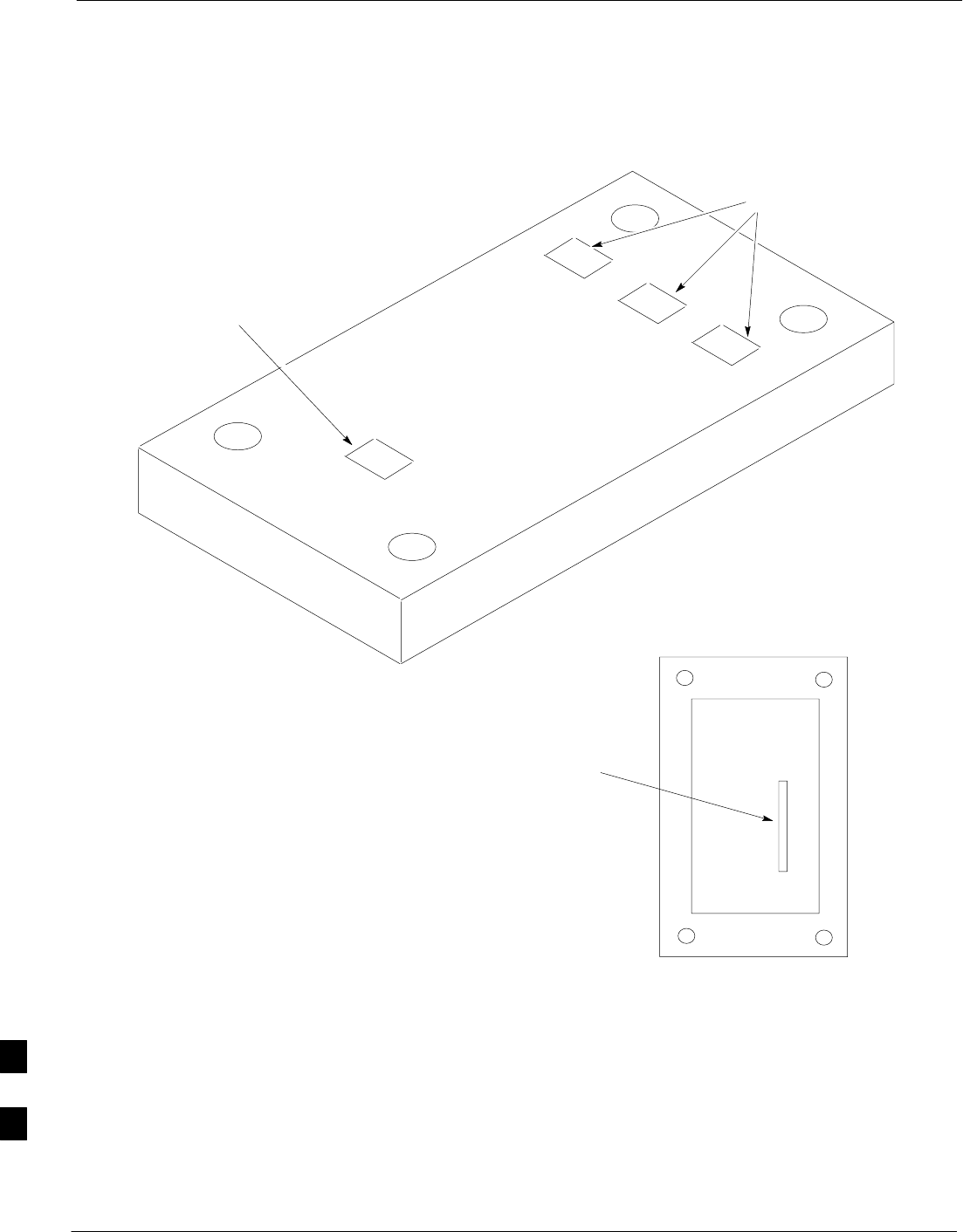
SDCX Module – continued
9-52 1X SC480 BTS Hardware Installation, Optimization/ATP, and FRU Jun 2004
DRAFT
Figure 9-18: SDCX Module
BOTTOM VIEW
Connector
Plug
Expansion SDC
Connectors
RGPS
TAIL
Connector
Used only if the site is
configured for multiple BTSs.
9
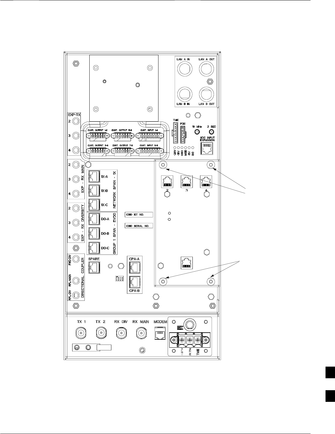
SDCX Module – continued
Jun 2004 1X SC480 BTS Hardware Installation, Optimization/ATP, and FRU 9-53
DRAFT
Figure 9-19: CBIO Board with SDCX
13003_001C
Remove
screws
Remove
screws
DAISY–CHAIN SYNC – OUT
SDCX KIT NO.
SDCX SERIAL NO.
DAISY–CHAIN POWER
SDCX POWER
EXPANSION FRAME SYNC – OUT
RF–GPS IN
PWR
25
25A
9
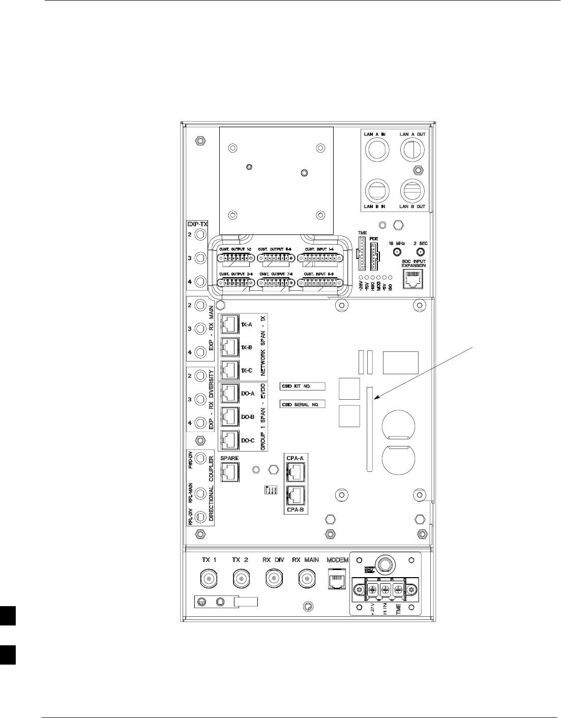
SDCX Module – continued
9-54 1X SC480 BTS Hardware Installation, Optimization/ATP, and FRU Jun 2004
DRAFT
Figure 9-20: CBIO Board with SDCX Removed
SDCX Board
connector
ti–cdma–wp–00311–v01–ildoc–ah
RF–GPD IN
PWR
25A 25
9
RF Filter Tray
Jun 2004 1X SC480 BTS Hardware Installation, Optimization/ATP, and FRU 9-55
DRAFT
Introduction
The procedures in this section cover only the removal and installation of
the RF Filter Tray.
System Impact/Considerations
If either of the filters on the tray is failing or has failed there will be an
interruption in call processing. The entire site will be down for
replacement of this component.
Required Items
Documents
None
Tools
Screwdriver with T20 star bit
Replacement Items
S1.9 GHz Filter Kit – 0 cCLPA (SGLN6221)
S1.9 GHz Filter Kit – 1 cCLPA (SGLN6220)
S1.9 GHz Filter Kit – 2 cCLPA (SGLN6219)
Prerequisite
Coordinate this repair task with the OMC–R operator.
IMPORTANT
*
Contact the OMC–R operator before performing the replacement
procedure. Tell the operator that the Filter Tray will be replaced and that
alarms can be expected.
Upon completion of the replacement procedure, have the OMC–R
operator verify that old alarms are cleared and that no new ones are
reported.
Replacement Procedure
If desired, record the BTS and Filter Tray serial number of the failed unit
in Table 9-66 at the end of this chapter.
If the BTS is in an outdoor configuration, perform Table 9-51, Remove
TME. The BTS removal is embedded in the procedure.
Remove Filter Tray
Follow the procedure in Table 9-30 to remove the Filter Tray.
9

RF Filter Tray – continued
9-56 1X SC480 BTS Hardware Installation, Optimization/ATP, and FRU Jun 2004
DRAFT
To perform the following procedure, the BTS must be
removed from the Mounting Plate.
NOTE
Table 9-30: Preparation Procedure for Removing the Filter Tray
Step Action
1Notify operator that the Filter Kit replacement procedure is starting and that alarms can be expected.
2Perform the Site Shutdown procedure in Table 10-2.
3Remove 3 M6 screws and washers securing BTS to Mounting Plate.
n WARNING
By pulling out the circuit breaker, power to the BTS will be interrupted, causing the BTS to go off
line.
4Disengage DC power to the BTS by pulling out the 20 A breaker at the rear of the BTS.
5If possible, turn off DC power at the source. Verify that DC Power source is OFF.
6Disconnect all cabling to the BTS.
7Remove BTS from Mounting Plate and place on a stable, flat surface.
8Put on an ESD wrist strap or other approved grounding device.Ensure wrist strap is properly
grounded. Do not ground to BTS chassis.
9If not already done, remove BTS front cover panel by grasping finger grooves at the top and bottom
and pulling.
10 Pull out all the circuit cards and modules.
11 If not already done, remove HSO Module cover panel by turning latch, gently pulling it open, and
sliding it out towards the right. The panel has a flange that fits into a slot in the chassis.
12 Reach fingers in along the right side and feel for the clip that holds on the lower front right side vent
panel, and pop out the panel.
13 Using the hole left by the front right side vent panel, reach fingers in along the divider and press on
the clip holding the rear right side vent panel and pop it out.
14 If the BTS is equipped with Filter Tray Kit SGLN6221, proceed to Table 9-31.
If the BTS is equipped with Filter Tray Kit SGLN6220, proceed to Table 9-35.
If the BTS is equipped with Filter Tray Kit SGLN6219, proceed to Table 9-37.
Filter Tray Kit SGLN6221
Removal Procedure
Follow the procedure in Table 9-31 to remove the Filter Tray.
9

RF Filter Tray – continued
Jun 2004 1X SC480 BTS Hardware Installation, Optimization/ATP, and FRU 9-57
DRAFT
Table 9-31: Procedure to Remove Filter Tray Kit SGLN6221
Step Action
1Perform the preparation procedure described in Table 9-30.
2Using a screwdriver with T20 star bit, remove two screws securing the Filter Tray Assembly to the
chassis.
3Disconnect the RF cables (Input) in the following order:
– RX MAIN connector (blue)
RX DIV connector (green)
RX RFL–MAIN connector (blue)
RX RFL–DIV connector (green)
RX FWD–DIV connector (green)
4Hold cables to one side and slide out filter tray to expose cables attached to rear connector (Output) of
each filter.
5Disconnect RX MAIN cable (blue).
6Disconnect RX DIV cable (green).
7Remove Filter Tray completely.
cMPC Cable Clip Removal
Procedure
Follow the procedure in Table 9-32 to remove the cMPC cable clip. The
cMPC cable clip is located just inside the front of the BTS, on the CCP2
shelf on the right side (looking into the BTS).
Table 9-32: Procedure to Remove cMPC Cable Clip
Step Action
NOTE
cMPC cable clip only needs to be removed if filter tray is not replaced with the same type. Clip
removal is to accommodate other filter tray configurations or cable replacement.
1Using a small, flat blade screwdriver, reach in and simultaneously lift tab and push towards the front
of the BTS. See Figure 9-21.
2Using thumb and forefinger grasp tab (narrow end), and pull up and towards rear to pop out clip.
3Remove clip and place a side.
4Remove the RX MAIN (blue) and RX DIV (green) cables.
9
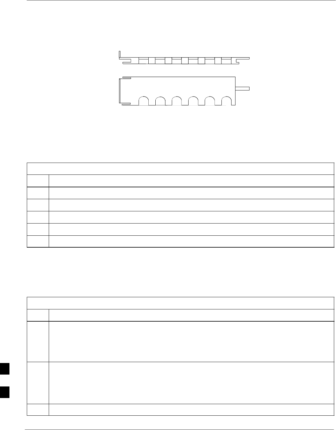
RF Filter Tray – continued
9-58 1X SC480 BTS Hardware Installation, Optimization/ATP, and FRU Jun 2004
DRAFT
Figure 9-21: cMPC Cable Clip
SLOT1 SLOT6
TOWARDS
FRONT OF BTS
TOWARDS
REAR OF BTS
cMPC Cable Clip Installation
Procedure
Follow the procedure in Table 9-33 to install the cMPC cable clip.
Table 9-33: Procedure to Install cMPC Cable Clip
Step Action
1Properly position cables in clip (order defined in installation procedure).
2Insert clip by sliding in wide flange end in first (towards front of BTS)
3Using a thumb, press on clip and push towards rear, slipping clip into place.
4Route cables inside BTS towards filter tray.
5Return to filter tray installation procedure.
Install Filter Tray Kit SGLN6221
Follow the procedure in Table 9-34 to install the Filter Tray. Refer to
Figure 9-22.
Table 9-34: Procedure to Install Filter Tray Kit SGLN6221
Step Action
1Put on an ESD wrist strap or other approved grounding device. Ensure that wrist strap is properly
grounded.
NOTE
Do not attach ESD wrist strap to BTS chassis.
2If not already installed, the following cables must be installed:
– RX RFL–MAIN (blue)
– RX RFL–DIV (green)
– RX FWD–DIV (green)
3Remove the CBIO Board by performing the procedure described in Table 9-26.
table continued on next page
9

RF Filter Tray – continued
Jun 2004 1X SC480 BTS Hardware Installation, Optimization/ATP, and FRU 9-59
DRAFT
Table 9-34: Procedure to Install Filter Tray Kit SGLN6221
Step Action
4Connect cables to the RFL–MAIN, RFL–DIV, and FWD–DIV connectors at the inside rear of the
BTS, respectively. Use a 5/16–in wrench to secure cables to connectors. Torque to 1 N–M.
NOTE
Cables have two heat shrink sleeves with a slight separation between them. The cMPC cable clip
slides into this separation to hold the cables in place.
5Install RX MAIN and RX DIV cables as follows:
– Ensuring the cable is on the inside of BTS, place RX DIV (green) cable into slot 1 of cMPC cable
clip (Connector labeled RX DIV faces towards the front of BTS)
– Place RX MAIN (blue) cable into slot 2 of cMPC cable clip (Connector labeled RX MAIN faces
towards the front of BTS).
– Place (red) cable into slot 5.
– Place (black) cable into slot 6.
6Perform Table 9-33 to install the cMPC cable clip. (If it had been removed.)
7Set Filter Tray on the edge of its slot and connect the RX MAIN (blue) and RX DIV (green) cables to
the output connector at the rear of their respective filters. See Figure 9-22.
8Slide Filter Tray into BTS chassis and secure using 2 M4 screws. Torque to 2.3 N–M (20 in–lbs).
9Connect the following cables:
– RX MAIN (blue) to RX MAIN input
– RX DIV (green) to RX DIV input
– RX RFL–MAIN (blue) to RFL–MAIN input
– RX RFL–DIV (green) to RFL–DIV input
– RX FWD–DIV (green) to FWD–DIV input
See Figure 9-22.
10 Use tie–wraps to dress cables as necessary.
11 Install the rear right side vent panel. Ensure that the clip end faces the front of the BTS or towards the
left.
12 Install the front right side vent panel. Ensure that the clip end faces the front of the BTS or towards the
left.
13 Make sure the vent panels are flush with the side of the BTS.
14 Install CBIO Board following the procedure in Table 9-27.
15 Install circuit cards and modules, ensure they are seated properly.
16 Install HSO Module cover panel by sliding its flange into the slot, closing, and latching it in place.
17 Disengage from the ESD wrist strap.
18 Set the BTS on the Mounting Plate and secure using 3 M6 screws and isolation washers. Torque to 5
N–M (44 in–lbs).
table continued on next page
9

RF Filter Tray – continued
9-60 1X SC480 BTS Hardware Installation, Optimization/ATP, and FRU Jun 2004
DRAFT
Table 9-34: Procedure to Install Filter Tray Kit SGLN6221
Step Action
19 Connect all external cabling.
20 Verify that DC power source is OFF before re–connecting to the BTS.
Turn on DC power source.
21 Notify the operator know that the replacement procedure is completed, and that power up will begin
shortly.
22 Allow the BTS to power up by pushing in the 20 A circuit breaker at the rear of the BTS.
23 Perform the Site Startup procedure in Table 10-5.
24 Perform an optimization of the cards, using the procedures in the Optimization/ATP section of this
manual.
25 After BTS is optimized, and it is operating within normal parameters, install the BTS front cover
panel by setting it in place and pushing on the top and bottom simultaneously.
26 Notify operator that optimization is complete.
9
RF Filter Tray – continued
Jun 2004 1X SC480 BTS Hardware Installation, Optimization/ATP, and FRU 9-61
DRAFT
Figure 9-22: Filter Tray Connectors and Cable Part Numbers (SGLN6221)
RX DIV
Cable PN 3086617X05
RFL–MAIN
Cable PN
3086617X07
RX MAIN
Cable PN
3086617X04
FWD–DIV
Cable PN
3086617X18
RFL–DIV
Cable PN 3086617X08
Front View
Input Connectors
Rear View
Output Connectors
RX DIV
Cable PN 3086617X02 RX MAIN
Cable PN 3086617X03
Filter Tray Kit SGLN6220
Removal Procedure
Follow the procedure in Table 9-35 to remove the Filter Tray Kit.
Table 9-35: Procedure to Remove Filter Tray Kit SGLN6220
Step Action
1Perform the preparation procedure described in Table 9-30.
2Using a screwdriver with T20 star bit, remove two screws securing the Filter Tray Assembly to the
chassis.
table continued on next page
9
RF Filter Tray – continued
9-62 1X SC480 BTS Hardware Installation, Optimization/ATP, and FRU Jun 2004
DRAFT
Table 9-35: Procedure to Remove Filter Tray Kit SGLN6220
Step Action
3Disconnect the RF cables (Input) in the following order:
– RX MAIN connector (blue) from RX MAIN connector
RX DIV connector (green)
RX RFL–DIV connector (green)
RX FWD–DIV connector (green)
See Figure 9-23
4Hold cables to one side and slide out filter tray to expose cable attached to rear connector (Output) of
the RX DIV filter.
5Disconnect RX DIV (Output) cable (green).
6Remove Filter Tray completely.
Figure 9-23: Filter Tray Connectors and Cable Part Numbers (SGLN6220)
RX DIV
Cable PN 3086617X05
RX MAIN
(from input)
Cable PN
3086617X35 FWD–DIV
Cable PN
3086617X18
RFL–DIV
Cable PN 3086617X08
Front View
Input Connectors
RX MAIN
(from output)
Cable PN
3086617X04
RX DIV
Cable PN 3086617X02
Rear View
Output Connector
9

RF Filter Tray – continued
Jun 2004 1X SC480 BTS Hardware Installation, Optimization/ATP, and FRU 9-63
DRAFT
Install Filter Tray Kit SGLN6220
Follow the procedure in Table 9-36 to install the Filter Tray. Refer to
Figure 9-22.
Table 9-36: Procedure to Install Filter Tray Kit SGLN6220
Step Action
1Put on an ESD wrist strap or other approved grounding device. Ensure that wrist strap is properly
grounded.
NOTE
Do not attach grounding devices to BTS chassis.
2If the filter tray to be installed is different from the one removed, proceed to the appropriate filter tray
installation procedure. Otherwise, proceed to step 5.
3If not already installed, the following cables must be installed:
– RX RFL–DIV (green)
– RX FWD–DIV (green)
4Remove the CBIO Board by performing the procedure described in Table 9-26.
5Connect cables to the RFL–DIV and FWD–DIV connectors, respectively. Use a 5/16–in wrench to
secure cables to connectors. Torque to 1 N–M.
NOTE
Cables have two heat shrink sleeves with a slight separation between them. The cMPC cable clip
slides into this separation to hold the cables in place.
6Install RX MAIN and RX DIV cables as follows:
– Ensuring the cable is on the inside of BTS, place RX DIV (green) cable into slot 1 of cMPCcable
clip (Connector labeled RX DIV faces towards the front of BTS)
– Place RX MAIN (blue) cable into slot 2 of cMPC cable clip (Connector labeled RX MAIN faces
towards the front of BTS).
– Place (red) cable into slot 5.
– Place (black) cable into slot 6.
7Perform Table 9-33 to install the cMPC cable clip.
8Set new Filter Tray into its slot and connect the input RX MAIN (blue) directly to output RX MAIN
cable. Connect RX DIV (green) cable to the output connector at the rear of the RX DIV filter. See .
9Slide Filter Tray into BTS chassis and secure using 2 M4 screws. Torque to 2.3 N–M (20 in–lbs).
10 Connect the following cables:
– RX DIV (green) to RX DIV input
– RX RFL–DIV (green) to RFL–DIV input
– RX FWD–DIV (green) to FWD–DIV input
See Figure 9-23.
11 Use tie–wraps to dress cables as necessary.
table continued on next page
9

RF Filter Tray – continued
9-64 1X SC480 BTS Hardware Installation, Optimization/ATP, and FRU Jun 2004
DRAFT
Table 9-36: Procedure to Install Filter Tray Kit SGLN6220
Step Action
12 Install the rear right side vent panel. Ensure that the clip end faces the front of the BTS or towards the
left.
13 Install the front right side vent panel. Ensure that the clip end faces the front of the BTS or towards the
left.
14 Make sure the vent panels are flush with the side of the BTS.
15 Install CBIO Board following the procedure in Table 9-27.
16 Install circuit cards and modules, ensure they are seated properly.
17 Install HSO Module cover panel by sliding its flange into the slot, closing, and latching it in place.
18 Disengage from the ESD wrist strap.
19 Set the BTS on the Mounting Plate and secure using 3 M6 screws and isolation washers. Torque to 5
N–M (44 in–lbs).
20 Connect all external cabling.
21 Verify that DC power source is OFF before re–connecting to the BTS.
Turn on DC power source.
22 Notify the operator know that the replacement procedure is completed, and that power up will begin
shortly.
23 Allow the BTS to power up by pushing in the 20 A circuit breaker at the rear of the BTS.
24 Perform the Site Startup procedure in Table 10-5.
25 Perform an optimization of the cards, using the procedures in the Optimization/ATP section of this
manual.
26 After BTS is optimized, and it is operating within normal parameters, install the BTS front cover
panel by setting it in place and pushing on the top and bottom simultaneously.
27 Notify operator that optimization is complete.
Filter Tray Kit SGLN6219
Removal Procedure
Follow the procedure in Table 9-37 to remove the Filter Tray Kit.
9

RF Filter Tray – continued
Jun 2004 1X SC480 BTS Hardware Installation, Optimization/ATP, and FRU 9-65
DRAFT
Table 9-37: Procedure to Remove Filter Tray Kit SGLN6219
Step Action
1Perform the preparation procedure described in Table 9-30.
2Disconnect the cables in the following order:
– RX MAIN connector (X35, blue) from RX MAIN (X04, blue) connector
RX DIV connector (X36, green) from RX DIV (X05, green) connector
See Figure 9-24.
3Remove cMPC cable clip per Table 9-32, if necessary
Install Filter Tray Kit SGLN6219
Follow the procedure in Table 9-38 to install the Filter Tray.
Table 9-38: Procedure to Install Filter Tray Kit SGLN6222 or SGLN6219
Step Action
1Put on an ESD wrist strap or other approved grounding device. Ensure that wrist strap is properly
grounded.
NOTE
Do not attach ESD wrist strap to BTS chassis.
2If the filter tray to be installed is different from the one removed, proceed to the appropriate filter tray
installation procedure. Otherwise, proceed to step 5.
NOTE
Cables have two heat shrink sleeves with a slight separation between them. The cMPC cable clip
slides into this separation to hold the cables in place.
3Install RX MAIN and RX DIV cables as follows:
– Ensuring the cable is on the inside of BTS, place RX DIV (green) cable into slot 1 of cMPC cable
clip (Connector labeled RX DIV faces towards the front of BTS)
– Place RX MAIN (blue) cable into slot 2 of cMPC cable clip (Connector labeled RX MAIN faces
towards the front of BTS).
– Place (red) cable into slot 5.
– Place (black) cable into slot 6.
See Figure 9-24.
4Perform Table 9-33 to install the cMPC cable clip. (If it had been removed.)
5Connect the input RX MAIN (blue) directly to output RX MAIN cable. Connect input RX DIV
(green) directly to the output RX DIV cable
6Use tie–wraps to dress cables as necessary.
7Install the rear right side vent panel. Ensure that the clip end faces the front of the BTS or towards the
left.
table continued on next page
9

RF Filter Tray – continued
9-66 1X SC480 BTS Hardware Installation, Optimization/ATP, and FRU Jun 2004
DRAFT
Table 9-38: Procedure to Install Filter Tray Kit SGLN6222 or SGLN6219
Step Action
8Install the front right side vent panel. Ensure that the clip end faces the front of the BTS or towards the
left.
9Make sure the vent panels are flush with the side of the BTS.
10 Install circuit cards and modules, ensure they are seated properly.
11 Install HSO Module cover panel by sliding its flange into the slot, closing, and latching it in place.
12 Disengage from the ESD wrist strap.
13 Set the BTS on the Mounting Plate and secure using 3 M6 screws and isolation washers. Torque to
5 N–M (44 in–lbs).
14 Connect all external cabling.
15 Verify that DC power source is OFF before re–connecting to the BTS.
Turn on DC power source.
16 Notify the operator know that the replacement procedure is completed, and that power up will begin
shortly.
17 Allow the BTS to power up by pushing in the 20 A circuit breaker at the rear of the BTS.
18 Perform the Site Startup procedure in Table 10-5.
19 Perform an optimization of the cards, using the procedures in the Optimization/ATP section of this
manual.
20 After BTS is optimized, and it is operating within normal parameters, install the BTS front cover
panel by setting it in place and pushing on the top and bottom simultaneously.
21 Notify operator that optimization is complete.
Figure 9-24: Filter Tray Connectors and Cable Part Numbers (SGLN6219)
RX MAIN (from input)
Cable PN 3086617X35
Front View
Input Connectors
RX MAIN (from output)
Cable PN 3086617X04 RX DIV (from input)
Cable PN 3086617X36
RX DIV (from output)
Cable PN 3086617X05
9
Compact Combined Linear Power Amplifier
Jun 2004 1X SC480 BTS Hardware Installation, Optimization/ATP, and FRU 9-67
DRAFT
Introduction
The procedures in this section cover only the removal and installation of
the Compact Combined Linear Power Amplifier (cCLPA).
System Impact/Considerations
If the cCLPA is failing or has failed there will be an interruption in call
processing. While the BTS itself may be operational, there may not be
reception or transmission depending on the fault.
Required Items
Documents
None
Tools
Screwdriver with T20 star bit
Replacement Item
S+27 VDC A Band (STTF4024)
S+27 VDC B Band (STTF4025)
S+27VDC 1.9 GHz (STTG4031)
Prerequisite
Coordinate this repair task with the OMC–R operator.
IMPORTANT
*
Contact the OMC–R operator before performing the replacement
procedure. Tell the operator that the Filter Tray will be replaced and that
alarms can be expected.
Upon completion of the replacement procedure, have the OMC–R
operator verify that old alarms are cleared and that no new ones are
reported.
Replacement Procedure
If desired, record the BTS and cCLPA serial number of the failed unit in
Table 9-67 at the end of this chapter.
Remove cCLPA
Follow the procedure in Table 9-39 to remove the cCLPA.
Table 9-39: Procedure to Remove cCLPA
Step Action
1Notify operator that the cCLPA replacement procedure is starting and that alarms can be expected.
2Have OMC–R operator disable the cCLPA and the associated BBX card(s).
table continued on next page
9

Compact Combined Linear Power Amplifier – continued
9-68 1X SC480 BTS Hardware Installation, Optimization/ATP, and FRU Jun 2004
DRAFT
Table 9-39: Procedure to Remove cCLPA
Step Action
3Turn off DC power to the cCLPA. For Outdoor configuration disengage the PDE circuit breaker to the
cCLPA being removed.
4Use a screwdriver with a T20 star bit to remove 8 screws securing I/O Board cover to the cCLPA.
5Loosen screws securing DC power to the I/O Board DC connector.
6Disconnect BTS Data Cable from the I/O Board.
7Disconnect ground cable from the cCLPA.
8Remove 4 M6 screws securing cCLPA to the rack.
9Loosen 2 M6 screws securing cCLPA flange to the rack enough to safely remove the cCLPA.
10 Lift cCLPA up and away from the rack.
Install cCLPA
Follow the procedure in Table 9-40 to install the cCLPA.
Table 9-40: Procedure to Install cCLPA
Step Action
1Lift cCLPA up and hang on two screws. Ensure that all screw holes align, then tighten screws to
flange.
2Install 4 M6 screws and secure cCLPA to rack.
3Connect ground cable to cCLPA.
4Route BTS Data Cable through cCLPA DATA opening and connect to RJ45 connector on cCLPA I/O
Board.
5Route DC power cable through DC IN opening and insert in DC Power terminal board. Ensure that the
“–” wire goes to –48V and the “+” wire goes to 0V locations. Tighten the screws to secure the wires in
place.
6Install I/O Board cover panel and use a screwdriver with a T20 star bit to secure it to cCLPA using 8
M6 screws.
7On cCLPA, pull out 20A circut breaker.
8Turn on cCLPA DC power source.
9Allow the cCLPA to power up by pushing in the 20 A circuit breaker.
10 Notify OMC–R operator that the cCLPA replacement procedure is completed.
11 Have OMC–R operator enable cCLPA and associated BBX card(s) that were taken out–of–service and
verify that there are no new alarms.
9
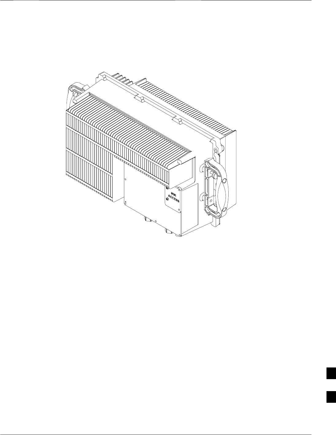
Compact Combined Linear Power Amplifier – continued
Jun 2004 1X SC480 BTS Hardware Installation, Optimization/ATP, and FRU 9-69
DRAFT
Figure 9-25: Compact Combined Linear Power Amplifier
ti–cdma–wp–00300–v01–ildoc–ah
9
TME Power Distribution Assembly
9-70 1X SC480 BTS Hardware Installation, Optimization/ATP, and FRU Jun 2004
DRAFT
Introduction
The procedures in this section cover only the removal and installation of
the TME Power Distribution Assembly (PDA)
System Impact/Considerations
If the PDA is failing or has failed there will be an interruption in call
processing. Power to the BTS and 1U unit will be interrupted.
Required Items
Documents
None
Tools
SScrewdriver with T20 star bit
STorque Driver Wrench or Torque Ratchet Wrench
SSocket, 8 mm, 3/8–in or 1/4–in
SFlat head or Phillips head screw driver
Replacement Item
SPDA (STHN4066A)
Prerequisite
Coordinate this repair task with the OMC–R operator.
IMPORTANT
*
Contact the OMC–R operator before performing the replacement
procedure. Tell the operator that the PDA will be replaced and that
alarms can be expected.
Upon completion of the replacement procedure, have the OMC–R
operator verify that old alarms are cleared and that no new ones are
reported.
9
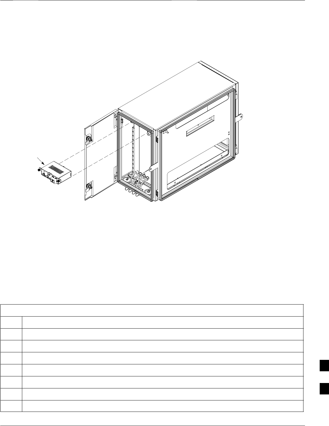
TME Power Distribution Assembly – continued
Jun 2004 1X SC480 BTS Hardware Installation, Optimization/ATP, and FRU 9-71
DRAFT
Figure 9-26: PDA Location
ti–cdma–wp–00262–v03–ildoc–ah
PDA
Replacement Procedure
If desired, record the BTS and PDA serial number of the failed unit in
Table 9-68 at the end of this chapter.
Remove PDA
Follow the procedure in Table 9-41 to remove the PDA. See Figure 9-26
or Figure 9-27.
Table 9-41: Procedure to Remove PDA
Step Action
1Notify operator that the PDA replacement procedure is starting and that alarms can be expected.
2Disengage circuit breakers setting to “O” position.
3Turn off DC power to the PDA.
4On PDA disconnect power plug from connector. Proceed to step 6.
5Use a screwdriver to loosen screws securing DC power wires to PDA.
6Use a wrench to remove two nuts and washers securing ground lug to the PDA.
7Loosen captive screws securing PDA to TME chassis.
table continued on next page
9

TME Power Distribution Assembly – continued
9-72 1X SC480 BTS Hardware Installation, Optimization/ATP, and FRU Jun 2004
DRAFT
Table 9-41: Procedure to Remove PDA
Step Action
8Gently pull out PDA far enough to disconnect cables at the rear.
9Remove PDA.
Install PDA
Follow the procedure in Table 9-42 to install the PDA. See Figure 9-26
or Figure 9-27.
Table 9-42: Procedure to Install PDA
Step Action
1Hold PDA near its slot in the TME and connect the cables (previously disconnected) to the rear of the
PDA.
2Slide PDA in and secure to TME chassis by tightening the captive screws.
3Place ground lug on ground studs of the PDA and secure using two M6 nuts and washers. Torque nuts
to 3.4 N–M (30 in–lbs).
4Verify that circuit breakers are disengaged (pulled out or set to “O” position).
5Verify that DC power source is OFF.
6Connect +27 V power plug.
7Turn on DC power.
8On PDA, set circuit breaker switch to “1” position.
9Push in 1U circuit breaker.
10 Notify operator that replacement is complete and verify that no new alarms have been generated and
that old alarms are cleared.
9
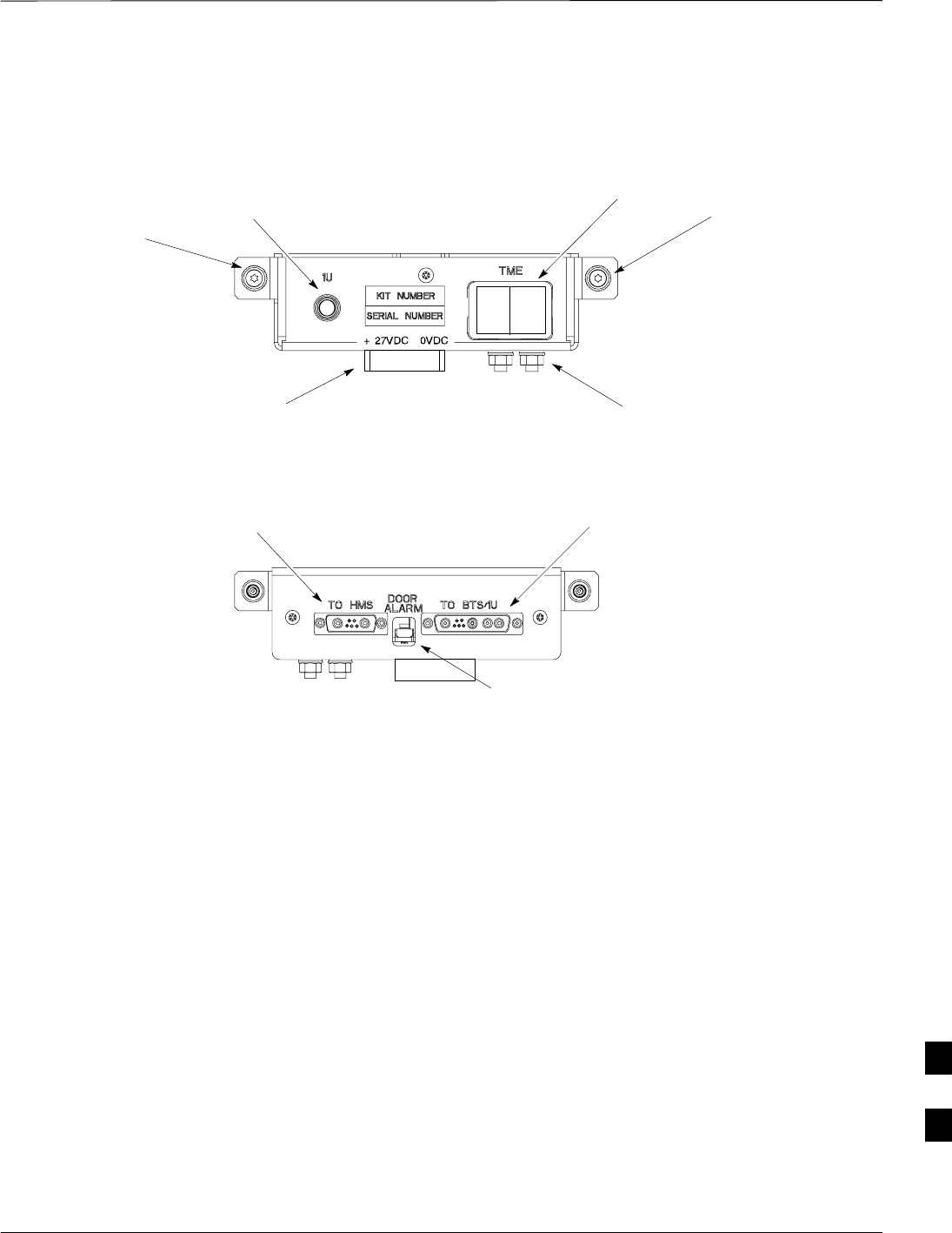
TME Power Distribution Assembly – continued
Jun 2004 1X SC480 BTS Hardware Installation, Optimization/ATP, and FRU 9-73
DRAFT
Figure 9-27: Power Distribution Assembly
Captive
Screw
Captive
Screw
FRONT
ti–cdma–wp–00348–v01–ildoc–ah
ti–cdma–wp–00346–v01–ildoc–ah
REAR
Ground
Location
1U
Circuit
Breaker
TME Circuit
Breaker
(Rocker Style)
TME Door Alarm
Connection
BTS / 1U
Connection
HMS
Connection
+27 VDC
Connector
Socket
9

Heat Management System
9-74 1X SC480 BTS Hardware Installation, Optimization/ATP, and FRU Jun 2004
DRAFT
Introduction
The procedures in this section cover only the removal and installation of
the Heat Management System (HMS)
System Impact/Considerations
If the HMS is failing or has failed there will be an interruption in call
processing. It is recommended that power be disengaged from the TME.
Required Items
Documents
None
Tools
SScrewdriver with T20 star bit
STorque Driver Wrench or Torque Ratchet Wrench
SSocket, 10 mm, 3/8–in or 1/4–in
Replacement Item
SHMS
SHeater Elements
SBlower Fan
SHMS Controller
Periodic Maintenance
The louvers over the HMS intake fan need to be inspected and cleaned in
order to ensure proper operation of the TME/BTS. A vacuum cleaner or
soft bristle brush is recommended to clean the louvers.
The condition of the louvers must be monitored. The
recommended service interval is every 90 days, barring any
previous inspections. Once environmental conditions at the
site are established by inspection, it is possible that
cleaning intervals may need to be adjusted to more or less
than the nominal 90 day interval.
NOTE
Prerequisite
Coordinate this repair task with the OMC–R operator.
IMPORTANT
*
9
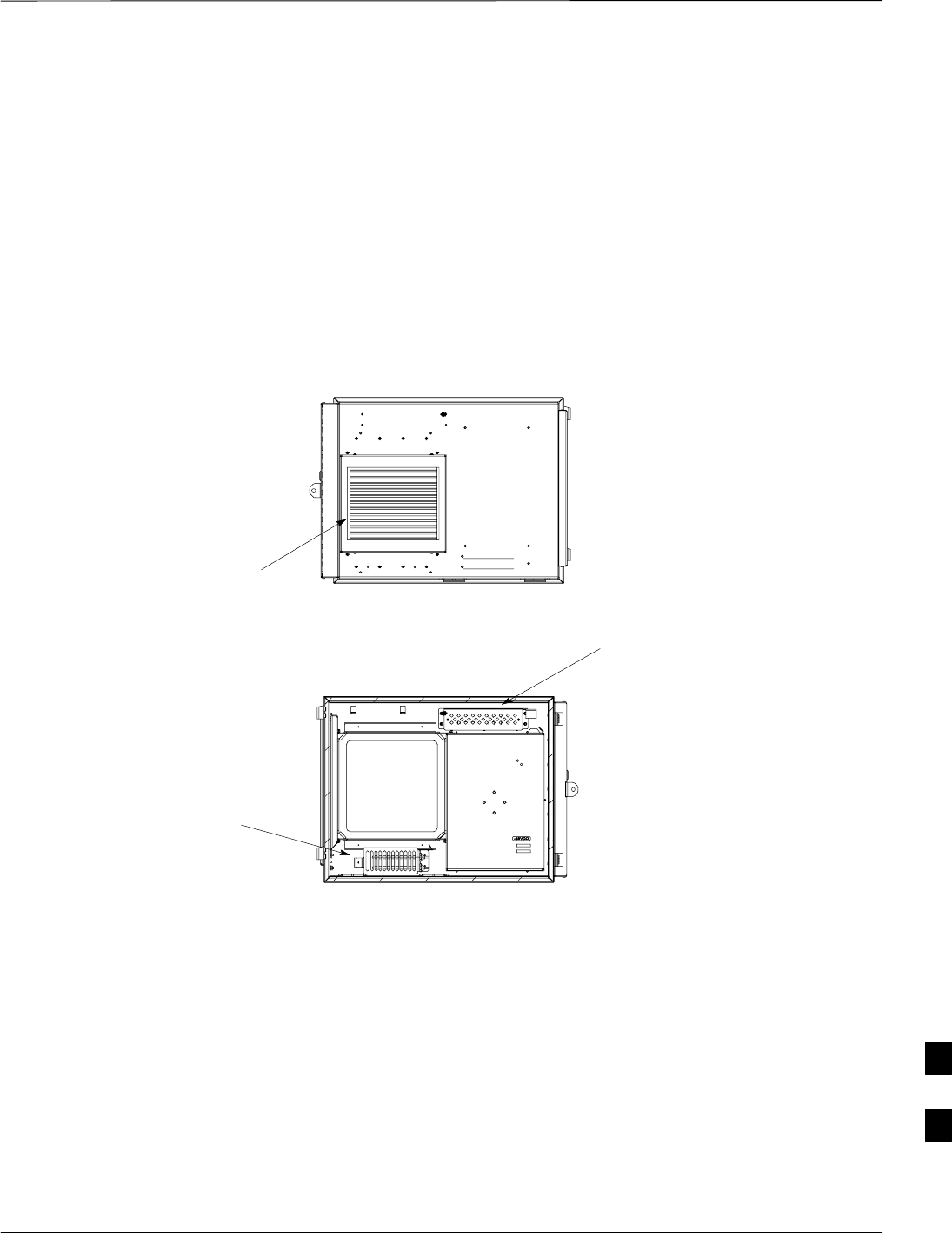
Heat Management System – continued
Jun 2004 1X SC480 BTS Hardware Installation, Optimization/ATP, and FRU 9-75
DRAFT
Contact the OMC–R operator before performing the replacement
procedure. Tell the operator that the HMS or its components will be
replaced and that alarms can be expected.
Upon completion of the replacement procedure, have the OMC–R
operator verify that old alarms are cleared and that no new ones are
reported.
Figure 9-28:Heat Management System
ti–cdma–wp–00337–v01–ildoc–ah
Blower
(Behind Louvers)
HMS
Controller
Heater
Elements
Replacement Procedure
If desired, record the TME and HMS serial number of the failed unit in
Table 9-69 at the end of this chapter.
Remove HMS
Follow the procedure in Table 9-43 to remove the HMS. See
Figure 9-28.
9

Heat Management System – continued
9-76 1X SC480 BTS Hardware Installation, Optimization/ATP, and FRU Jun 2004
DRAFT
Table 9-43: Procedure to Remove HMS
Step Action
1Notify operator that the HMS replacement procedure is starting and that alarms can be expected.
2Turn off DC power to the TME.
3Unlock and remove external lock
4Use key to unlock HMS draw latch door.
5Turn latches and slowly swing open HMS.
! CAUTION
Be aware of the heater elements, they will be hot to the touch if they have been in recent use.
Removing the HMS exposes the interior of the TME to the elements, cover the opening with a
blanket, towel, tarp, card board, or equivalent item.
6Use an driver wrench with socket to remove two M6 nuts and washers securing ground lug to HMS
door. Disconnect DC power and HMS controller cable from HMS Controller.
7Remove HMS and place on a flat surface, preferably a table of bench top.
! CAUTION
Be careful not to damage louvers protecting Blower Fan.
Install HMS
Follow the procedure in Table 9-44 to re–install the HMS.
Table 9-44: Procedure to Re–install HMS
Step Action
1Carefully lift HMS and set on TME hinge pins.
2Place ground lug on ground studs of the HMS and secure using two M6 nuts and washers. Torque nuts
to 3.4 N–M (30 in–lbs).
3Connect DC Power and HMS controller cable to HMS Controller.
4Close HMS be careful not to pinch any of the wiring.
5Close HMS and secure using the two draw latches. Fold draw latch handles down. Verify that HMS is
fully closed and seated.
6Close HMS draw latch door and lock using key.
7Lock HMS with external lock.
8Notify operator that replacement is complete and verify that no new alarms have been generated and
that old alarms are cleared.
9

Heat Management System – continued
Jun 2004 1X SC480 BTS Hardware Installation, Optimization/ATP, and FRU 9-77
DRAFT
Heater Element Replacement
Procedure
This information is still under consideration at this time. Updated
information will be supplied at a later date.
If desired, record the TME, HMS, and HMS Heater Elements serial
number of the failed unit in Table 9-70 at the end of this chapter.
Perform the procedure in Table 9-45 to remove the Heater Elements.
Table 9-45: Procedure to Replace Heater Elements
Step Action
1Perform the HMS removal procedure described in Table 9-43.
! CAUTION
Heater Elements could still be hot, use caution when removing them. Recommend that thermal
resistant gloves be worn to remove the heater elements.
2
3
4
5
Heater Element Installation
Procedure
This information is still under consideration at this time. Updated
information will be supplied at a later date.
Perform the procedure in Table 9-46 toinstall the Heater Elements.
Table 9-46: Procedure to Install Heater Elements
Step Action
1
2
3
4
5Perform the procedure in Table 9-44 to install the HMS.
9
Heat Management System – continued
9-78 1X SC480 BTS Hardware Installation, Optimization/ATP, and FRU Jun 2004
DRAFT
Figure 9-29: HMS Heater Elements
NOTE:
1. 8 point microdocument
2. 8 point microdocument
8 pt. Left Aligned text
8 pt. Right Aligned Text
8 pt. Centered Text
HMS Controller Replacement
Procedure
This information is still under consideration at this time. Updated
information will be supplied at a later date.
If desired, record the TME, HMS, and HMS Controller serial number of
the failed unit in Table 9-71 at the end of this chapter.
Perform the procedure in Table 9-47 to remove the HMS Controller.
Table 9-47: Procedure to Replace HMS Controller
Step Action
1Perform the HMS removal procedure described in Table 9-43.
2
3
4
5
HMS Controller Installation
Procedure
This information is still under consideration at this time. Updated
information will be supplied at a later date.
9
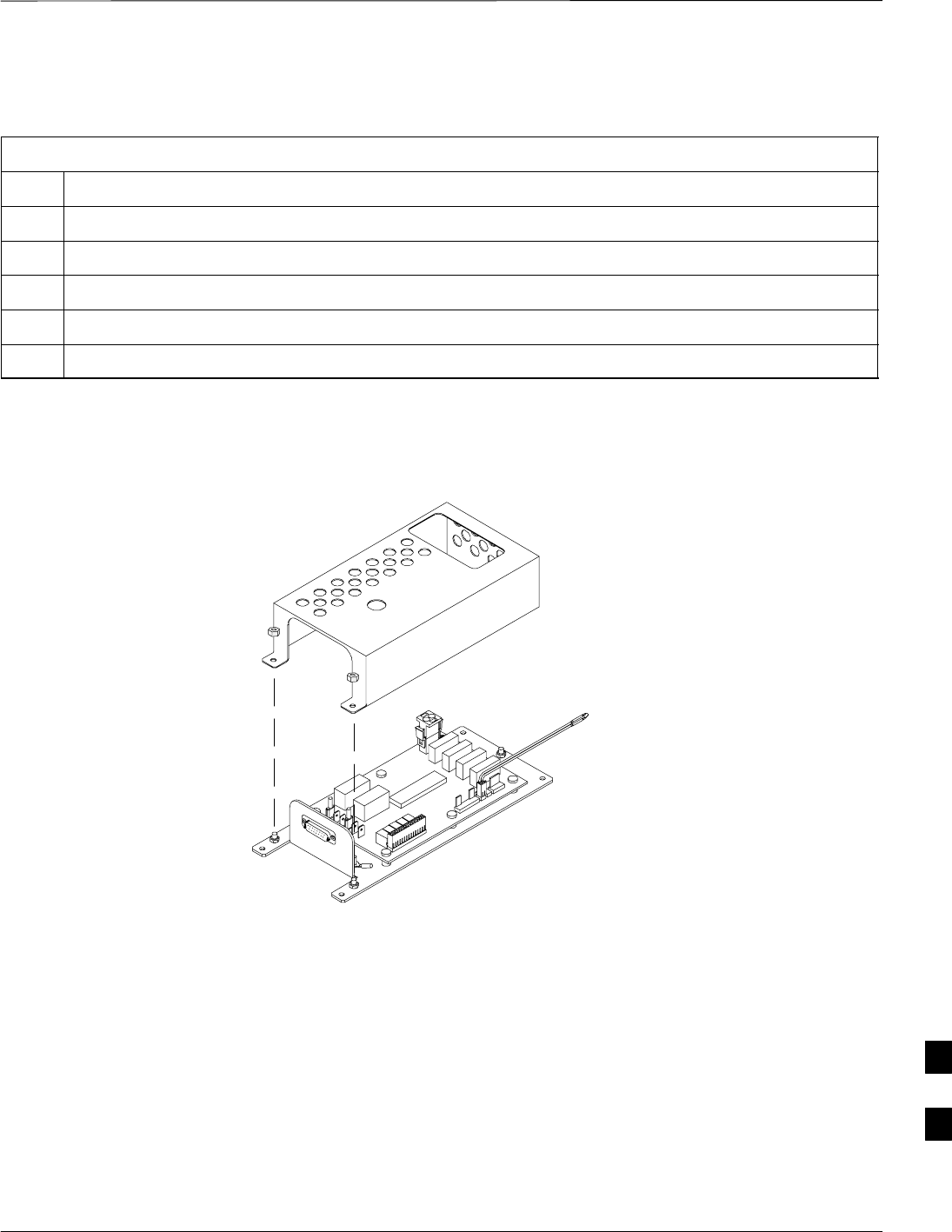
Heat Management System – continued
Jun 2004 1X SC480 BTS Hardware Installation, Optimization/ATP, and FRU 9-79
DRAFT
Perform the procedure in Table 9-48 to install the HMS Controller.
Table 9-48: Procedure to Install HMS Controller
Step Action
1
2
3
4
5Perform the procedure in Table 9-44 to install the HMS.
Figure 9-30: HMS Controller
ti–cdma–wp–00263–v01–ildoc–ah
Blower Fan Replacement
Procedure
This information is still under consideration at this time. Updated
information will be supplied at a later date.
If desired, record the TME, HMS, and Blower Fan serial number of the
failed unit in Table 9-72 at the end of this chapter.
Perform the procedure in Table 9-47 to remove the Blower Fan.
9

Heat Management System – continued
9-80 1X SC480 BTS Hardware Installation, Optimization/ATP, and FRU Jun 2004
DRAFT
Table 9-49: Procedure to Replace Blower Fan
Step Action
1Perform the procedure in Table 9-43 to remove the HMS.
2
3
4
5
Blower Fan Installation
Procedure
This information is still under consideration at this time. Updated
information will be supplied at a later date.
Perform the procedure in Table 9-48 to install the Blower Fan.
Table 9-50: Procedure to Install Blower Fan
Step Action
1
2
3
4
5Perform the procedure in Table 9-44 to install the HMS.
9

Heat Management System – continued
Jun 2004 1X SC480 BTS Hardware Installation, Optimization/ATP, and FRU 9-81
DRAFT
Figure 9-31: Blower Fan
NOTE:
1. 8 point microdocument
2. 8 point microdocument
8 pt. Left Aligned text
8 pt. Right Aligned Text
8 pt. Centered Text
9
Thermal Management Enclosure
9-82 1X SC480 BTS Hardware Installation, Optimization/ATP, and FRU Jun 2004
DRAFT
Introduction
The procedures in this section cover only the removal and installation of
the Thermal Management Enclosure (TME).
System Impact/Considerations
If the TME enclosure has been damaged it will no longer environmetally
protect the BTS. Thus, an interruption in call processingwill occur while
the TME is replaced.
Required Items
Documents
None
Tools
SScrewdriver with T20 star bit or T30 star bit
STorque Driver Wrench or Torque Ratchet Wrench
SSocket, 8 mm, 3/8–in or 1/4–in
S10 mm socket
Replacement Item
STME
Prerequisite
Coordinate this repair task with the OMC–R operator.
IMPORTANT
*
Contact the OMC–R operator before performing the replacement
procedure. Tell the operator that the Filter Tray will be replaced and that
alarms can be expected.
Upon completion of the replacement procedure, have the OMC–R
operator verify that old alarms are cleared and that no new ones are
reported.
Replacement Procedure
Remove TME
Follow the procedure in Table 9-51 to remove the TME.
Table 9-51: Procedure to Remove TME
Step Action
1Notify operator that TME replacement procedure is starting and that alarms can be expected.
2Perform Carrier Shutdown procedure as described in Table 10-4.
table continued on next page
9

Thermal Management Enclosure – continued
Jun 2004 1X SC480 BTS Hardware Installation, Optimization/ATP, and FRU 9-83
DRAFT
Table 9-51: Procedure to Remove TME
Step Action
3Disengage circuit breaker on the affected cCLPAs.
4Use the key to unlock both doors of the TME.
5Disengage TME PDA circuit breakers by pulling them out.
6At the rear of the BTS disconnect antenna cables from BTS to TME.
7If not already done, label individual cables as they are disconnected from the rear of the BTS.
8Remove cover and disconnect DC power cables from BTS.
9Use screwdriver to remove two screws securing ground lug to BTS.
10 Use key to unlock the HMS draw latch door.
11 Turn latches and open HMS.
12 Disconnect ground lug by removing two nuts and washers with the driver wrench and socket.
13 Disconnect DC power and HMS controller cable from HMS to TME.
14 Lift HMS off hinge pins on TME and place on a flat surface. See Figure 4-21.
! CAUTION
Be careful not to damage louvers protecting Blower Fan.
15 Remove 5 M6 screws securing BTS to TME. See Figure 4-19.
16 Slide BTS out of TME.
17 Disconnect all conduit hubs and cabling from bottom of TME. Label conduit and cabling as necessary.
18 Remove 6 M6 screws securing TME to Wall Mounting Bracket. See Figure 4-18.
19 Lift TME off of Wall Mounting Bracket.
Install TME
Follow the procedure in Table 9-52 to install the TME.
Table 9-52: Procedure to Install TME
Step Action
1Set the TME onto the Wall Mounting Bracket. Ensure that it rests in the slots of the Wall Mounting
Bracket. See Figure 4-17.
2Secure the TME to the Wall Mounting Bracket using 6 M6 screws. Torque screws to 3.4 N–M (30
in–lbs). See Figure 4-18.
3Place BTS in TME opening and slide it in.
4Secure BTS to TME using 5 M6 screws. Torque screws to 3.4 N–M (30 in–lbs). See Figure 4-19.
table continued on next page
9

Thermal Management Enclosure – continued
9-84 1X SC480 BTS Hardware Installation, Optimization/ATP, and FRU Jun 2004
DRAFT
Table 9-52: Procedure to Install TME
Step Action
5Insert cables from conduit up through their respective access holes and connect to the BTS.
6Tighten conduit hubs.
7Use a screw driver and two screws to secure the ground lug to the BTS.
8Connect antenna cables from BTS to TME.
9Connect all cabling to connectors on bottom of the TME.
10 Install DC power wires to BTS, use a screwdriver to tighten screws holding wires.
11 Install cover over BTS DC power connection.
12 Set HMS on hinges on TME.
13 Using the driver wrench and socket, attach ground lug to HMS using two nuts and washers.
14 Connect DC power and HMS controller cable.
15 Close HMS and secure using the two draw latches. Fold draw latch handles down. Verify that HMS is
fully closed and seated.
16 Close HMS draw latch door and lock using key.
17 Turn on DC power to TME.
18 Engage PDA circuit breakers (push in).
19 Engage circuit breaker on affected cCLPAs.
20 Notify operator that replacement is complete and verify that no new alarms have been generated and
that old alarms are cleared.
21 Perform Carrier Startup Procedure as described in Table 10-7.
9

Power Distribution Enclosure
Jun 2004 1X SC480 BTS Hardware Installation, Optimization/ATP, and FRU 9-85
DRAFT
Introduction
The procedures in this section cover only the removal and installation of
the Powerl Distribution Enclosure (PDE).
System Impact/Considerations
If the PDE enclosure has been damaged it will no longer environmetally
protect the AC–to–DC power converter circuitry. Thus, an interruption
in call processing will occur while the PDE is replaced.
Replacement Procedure
Consult the manufacturer’s Field Replacement Unit (FRU) guide for
removal and replacement information.
9

Master Item Number Failure List
9-86 1X SC480 BTS Hardware Installation, Optimization/ATP, and FRU Jun 2004
DRAFT
Introduction
The Master Item Number Failure List is provided as a means of keeping
a written record of the units that failed for any particular BTS or BTSes.
The list is for logistical purposes only.
For the BTS Fan Module, use Table 9-53.
Table 9-53: Fan Module Item Number List
Item Number
BTS Number
Fan Module Number
For the HSO/MSO Module, use Table 9-54.
Table 9-54: HSO or MSO Module Item Number List
Item Number
BTS Number
HSO Module Number
MSO Module Number
For the RGPS Head, use Table 9-55.
Table 9-55: RGPS Item Number List
Item Number
BTS Number
RGPS Head Number
For the RF GPS Module, use Table 9-56.
Table 9-56: RF GPS Module Item Number List
Item Number
BTS Number
RF GPS Number
9

Master Item Number Failure List – continued
Jun 2004 1X SC480 BTS Hardware Installation, Optimization/ATP, and FRU 9-87
DRAFT
For the PSM, use Table 9-57.
Table 9-57: PSM Item Number List
Item Number
BTS Number
PSM Number
For the CSA Card, use Table 9-58.
Table 9-58: CSA Card Item Number List
Item Number
BTS Number
CSA Card
For the GLI3 Card, use Table 9-59.
Table 9-59: GLI3 Card Item Number List
Item Number
BTS Number
GLI3 Card
For the MCC–1X, use Table 9-60.
Table 9-60: MCC–1X Card Item Number List
Item Number
BTS Number
MCC 1
MCC 2
MCC 3
9

Master Item Number Failure List – continued
9-88 1X SC480 BTS Hardware Installation, Optimization/ATP, and FRU Jun 2004
DRAFT
For the BBX–1X, use Table 9-61.
Table 9-61: BBX–1X Card Item Number List
Item Number
BTS Number
BBX 1 (SGLG4044)
BBX 4 (SGLG4044)
For the cMPC, use Table 9-62.
Table 9-62: Compact MPC Item Number List
Item Number
BTS Number
Compact MPC Number
For the MCC–DO card, use Table 9-63.
Table 9-63: MCC–DO Card Item Number List
Item Number
BTS Number
MCC–Data Only Card
For the CBIO Board, use Table 9-64.
Table 9-64: CBIO Board Item Number List
Item Number
BTS Number
CBIO Board
For the SDCX Module, use Table 9-65.
Table 9-65: SDCX Module Item Number List
Item Number
BTS Number
SDCX Number
9

Master Item Number Failure List – continued
Jun 2004 1X SC480 BTS Hardware Installation, Optimization/ATP, and FRU 9-89
DRAFT
For the Filter Tray, use Table 9-66.
Table 9-66: Filter Tray Kit Item Number List
Item Number
BTS Number
Filter Tray Kit (SGLN6221)
Filter Tray Kit (SGLN6220)
Filter Tray Kit (SGLN6219)
For the cCLPA, use Table 9-67.
Table 9-67: cCLPA Item Number List
Item Number
BTS Number
cCLPA #1 (If used)
cCLPA #2 (If used)
For the TME PDA, use Table 9-68.
Table 9-68: TME PDA Item Number List
Item Number
TME Number
PDA
For the TME HMS, use Table 9-69.
Table 9-69: TME HMS Item Number List
Item Number
TME Number
HMS Number
9

Master Item Number Failure List – continued
9-90 1X SC480 BTS Hardware Installation, Optimization/ATP, and FRU Jun 2004
DRAFT
For the TME HMS Heater Elements, use Table 9-70.
Table 9-70: TME HMS Heater Element Item Number List
Item Number
TME Number
HMS Number
Heater Element
For the TME HMS Controller, use Table 9-71.
Table 9-71: TME HMS Controller Item Number List
Item Number
TME Number
HMS Number
HMS Controller Number
For the TME HMS Blower Fan, use Table 9-72.
Table 9-72: TME HMS Blower Fan Item Number List
Item Number
TME Number
HMS Number
HMS Blower Fan Number
9

Jun 2004 1X SC480 BTS Hardware Installation, Optimization/ATP, and FRU
DRAFT
Chapter 10: Reference Procedures Performed At OMC–R
Table of Contents
Reference Procedures Performed At OMC–R 10-1 . . . . . . . . . . . . . . . . . . . . . . . . . .
Introduction 10-1 . . . . . . . . . . . . . . . . . . . . . . . . . . . . . . . . . . . . . . . . . . . . . .
Accessing OMC–R CLI Window 10-2 . . . . . . . . . . . . . . . . . . . . . . . . . . . . . . . . . . . .
Accessing OMC–R CLI Window 10-2 . . . . . . . . . . . . . . . . . . . . . . . . . . . . .
Circuit BTS Shut Down Procedures 10-3 . . . . . . . . . . . . . . . . . . . . . . . . . . . . . . . . . .
Shut Down Site Signaling Functions for a Circuit BTS 10-3 . . . . . . . . . . . .
Shut Down Sector Signaling Functions for a Circuit BTS 10-9 . . . . . . . . . .
Shut Down Carrier Signaling Functions for a Circuit BTS 10-16 . . . . . . . . . .
Circuit BTS Start–Up Procedures 10-23 . . . . . . . . . . . . . . . . . . . . . . . . . . . . . . . . . . . .
Restore Site Signaling Operations for a Circuit BTS 10-23 . . . . . . . . . . . . . .
Restore Sector Signaling Operations for a Circuit BTS 10-26 . . . . . . . . . . . .
Restore Carrier Signaling Operations for a Circuit BTS 10-29 . . . . . . . . . . . .
Packet BTS Shut Down Procedures 10-32 . . . . . . . . . . . . . . . . . . . . . . . . . . . . . . . . . .
Shut Down Site Signaling Functions for a Packet BTS 10-32 . . . . . . . . . . . .
Shut Down Sector Signaling Functions for a Packet BTS 10-39 . . . . . . . . . .
Shut Down Carrier Signaling Functions for a Packet BTS 10-46 . . . . . . . . . .
Packet BTS Start–Up Procedures 10-53 . . . . . . . . . . . . . . . . . . . . . . . . . . . . . . . . . . . .
Restore Site Signaling Operations for a Packet BTS 10-53 . . . . . . . . . . . . . .
Restore Sector Signaling Operations for a Packet BTS 10-56 . . . . . . . . . . . .
Restore Carrier Signaling Operations for a Packet BTS 10-59 . . . . . . . . . . . .
10

Table of Contents – continued
1X SC480 BTS Hardware Installation, Optimization/ATP, and FRU Jun 2004
DRAFT
Notes
10

Reference Procedures Performed At OMC–R
Jun 2004 1X SC480 BTS Hardware Installation, Optimization/ATP, and FRU 10-1
DRAFT
Introduction
The procedures in this chapter are referenced during various FRU
replacement procedures and are performed by the OMC–R operator.
These reference procedure covers the following:
SAccessing OMCR CLI window
SCircuit BTS shut down and restore procedures for:
– BTS
– Sector
– Carrier
SPacket BTS shut down and restore procedures for:
– BTS
– Sector
– Carrier
10
Accessing OMC–R CLI Window
10-2 1X SC480 BTS Hardware Installation, Optimization/ATP, and FRU Jun 2004
DRAFT
Accessing OMC–R CLI Window
Many of the FRU procedures require the OMC–R operator to manipulate
BTS logical devices. This is achieved via UNO or the OMC–R
(Operations and Maintenance Center – Radio) Command Line Interface
(CLI).
The operator enters commands via UNO or OMC–R CLI.
Should there be any issues which affect UNO or the
OMC–R CLI operations, command dependent replacement
procedures cannot be performed.
IMPORTANT
*
OMC–R CLI access procedure
The following procedure is performed by the OMC–R operator at the
OMC–R terminal.
Table 10-1: Login and Access Alarm Window Procedure
nStep Action
1Login by entering the user name.
2Enter the password at the system prompt.
3Open an UNO Alarm Manager window and an OMC–R CLI window from the pull down menu
using the mouse button.
4Verify that the filter display is set to the BTS–# where the work is being performed. This ensures
that any BTS–# alarms, encountered while installing the hardware, can be observed and rectified.
10
Circuit BTS Shut Down Procedures
Jun 2004 1X SC480 BTS Hardware Installation, Optimization/ATP, and FRU 10-3
DRAFT
Shut Down Site Signaling Functions for
a Circuit BTS
If a complete site shutdown is required for the FRU replacement, follow
the procedure in Table 10-2 to disable the circuit BTS site.
This site shut down procedure takes a BTS out–of–service
(OOS), but does not affect other BTSs. To minimize
system impact, it may be advisable (but not necessary) to
perform this procedure during a maintenance window.
CAUTION
The EDIT REDIRECT or REDIRECT2 command does
NOT affect calls in progress and does NOT move these
calls to another BTS. The command only prevents future
calls from being originated on the targeted BTS. If active
call processing is still taking place in the target BTS, wait
for any active calls to terminate before disabling the BTS.
IMPORTANT
*
Refer to the System Commands Reference manual
(68P09256A58) part/of Cellular System Administration
CDMA2000 1X – 99R09255A10 CD–ROM for a complete
explanation of OMCR commands.
NOTE
Table 10-2: Shut Down Site Signaling Functions Procedure For a Circuit BTS
nStep Action
1Open a CLI window. Refer to the Accessing OMC–R CLI Window section on page 10-2.
* IMPORTANT
It is recommended that you redirect subscribers to another site/carrier and then wait for any active
calls to terminate before disabling the BTS.
2If you want to redirect subscribers and then wait for any active calls to terminate before disabling
the BTS, go to step 3.
If you are not concerned about redirecting subscribers and waiting for any active calls to terminate
and you just want to disable the BTS, perform step 13 and step 15 only.
. . . continued on next page 10

Circuit BTS Shut Down Procedures – continued
10-4 1X SC480 BTS Hardware Installation, Optimization/ATP, and FRU Jun 2004
DRAFT
Table 10-2: Shut Down Site Signaling Functions Procedure For a Circuit BTS
nActionStep
NOTE
The REDIRECT command is used to redirect subscribers to an 1.9 GHz site or to invoke the
REDIRECT2 command which is then used to redirect subscribers to a different CDMA carrier
frequency. REDIRECT2 is the preferred command if an alternate CDMA carrier is available.
* IMPORTANT
Record the values shown in the following system display response. These values are used to
answer the prompts for the EDIT REDIRECT command when restoring signaling operations at the
end of the replacement procedure.
3View the status of the BTS signaling redirect parameters for all carriers equipped for the BTS by
entering the following command at the prompt:
omc–000000>DISPLAY BTS–<bts#> REDIRECT
Observe the following typical system display response for a BTS (this example shows initial
standard values):
Access Overload Class Redirect Flags
RETURN ROTATE RECORD EXP IGNORE SYS
CARRIER ID IF FAIL 0 0 0 0 0 0 0 0 0 0 1 1 1 1 1 1 TIMER TYPE SID CDMA ORDERING
(bts–sector–carrier) 0 1 2 3 4 5 6 7 8 9 0 1 2 3 4 5 (sec)
–––––––––––––––––––– ––––––– – – – – – – – – – – – – – – – – –––––– –––––– ––––– –––––– ––––––––
CARRIER–1–1–1 N N N N N N N N N N N N N N N N N 4 1 0 N CUSTOM
. . . continued on next page
10

Circuit BTS Shut Down Procedures – continued
Jun 2004 1X SC480 BTS Hardware Installation, Optimization/ATP, and FRU 10-5
DRAFT
Table 10-2: Shut Down Site Signaling Functions Procedure For a Circuit BTS
nActionStep
NOTE
This step edits the REDIRECT parameters so that the Global Service Redirect Message to be
broadcast on the paging channel redirects all subscribers away from the BTS and onto a different
BTS or system.
4Enter the following command at the prompt:
omc–000000>EDIT BTS–<bts#> REDIRECT!
The system prompts you to enter each command parameter value one at a time. Answer the
prompts in the following order:
<accolc0>enter Y, <accolc1>enter Y, ... <accolc15> enter Y
(All Access Overload Classes must be set to yes to ensure that all subscribers are redirected.)
<returniffail> , enter N
(Must be set to no to ensure that subscribers do not return if redirect is unsuccessful.)
<recordtype> , enter 1 or 2
(A value of 2 will invoke REDIRECT2 which is used to redirect subscribers to a CDMA channel
at a neighbor site. A value of 1 redirects subscribers to an 1.9 GHz site. This example uses 2.)
<expectedsid> , enter 13
(Use the Area ID the subscriber units should expect to find on the system where they are being
redirected. This example uses 13. The valid range is 0 – 32767; the default is 0.)
<ignorecdma> , enter Y
<sysordering> , enter CUSTOM
(The system acquisition ordering value tells the mobiles the order to use when attempting to
obtain service on the different analog systems. Valid values are: CUSTOM – use custom system
selection; AONLY – try the A system only; BONLY – use the B system only; AFIRST – try the A
system first. If unsuccessful, try the B system; BFIRST – try the B system first. If unsuccessful,
try the A system; AORB – try A or B. If unsuccessful try the alternative system; CUSTOM is the
default.)
<rotatetimer> , enter 4
(Call processing continuously rotates, circular right–shifts, the Y/N values of Access Overload
Class Redirect Flags 0 to 9. Values are shifted one flag at the end of the timer period; then timer
re–starts. Valid values are 0–255; 4 is the default.)
The system displays the command to be sent. Verify the command syntax.
omc–000000>Accept [yes/no]?
Enter Y to accept the command or N to go back and enter the correct value(s).
. . . continued on next page
10

Circuit BTS Shut Down Procedures – continued
10-6 1X SC480 BTS Hardware Installation, Optimization/ATP, and FRU Jun 2004
DRAFT
Table 10-2: Shut Down Site Signaling Functions Procedure For a Circuit BTS
nActionStep
5View the status of the signaling REDIRECT parameters to verify that the applicable BTS is ready
for global redirect.
omc–000000>DISPLAY BTS–<bts#> REDIRECT
Ensure that the values in the system display response match the values input in Step 4 (see
example below).
Access Overload Class Redirect Flags ROTATE
CARRIER ID RETURN 0 0 0 0 0 0 0 0 0 0 1 1 1 1 1 1 TIMER RECORD EXP IGNORE SYS
(bts–sector–carrier) IF FAIL 0 1 2 3 4 5 6 7 8 9 0 1 2 3 4 5 (SEC) TYPE SID CDMA ORDERING
–––––––––––––––––––– ––––––– – – – – – – – – – – – – – – – – ––––– –––– –––– ––– ––––––––
CARRIER–1–1–1 N Y Y Y Y Y Y Y Y Y Y Y Y Y Y Y Y 4 2 13 Y CUSTOM
6If 2 was entered for <recordtype> in step 4, go to step 7.
If 1 was entered for <recordtype> in step 4, go to step 10.
* IMPORTANT
Record the values shown in the following system display response. These values are used to
answer the prompts for the EDIT REDIRECT2 command when restoring signaling operations at
the end of the replacement procedure.
7View the status of the BTS signaling redirect parameters for all carriers equipped for the BTS by
entering the following command at the prompt:
omc–000000>DISPLAY BTS–<bts#> REDIRECT2
Observe the following typical system display response for a BTS (this example shows initial
standard values):
REDIRECT CHAN
CARRIER ID EXP BAND
(bts–sector–carrier) NID CLASS 1 2 3 4 5 6 7 8 9 10 11 12 13 14 15
–––––––––––––––––––– ––––– ––––––––– ––– ––– ––– ––– ––– ––– –––– –––– –––– –––– –––– –––– –––– ––– ––––
CARRIER–1–1–1 65535 CDMA800 – – – – – – – – – – – – – – –
. . . continued on next page
10

Circuit BTS Shut Down Procedures – continued
Jun 2004 1X SC480 BTS Hardware Installation, Optimization/ATP, and FRU 10-7
DRAFT
Table 10-2: Shut Down Site Signaling Functions Procedure For a Circuit BTS
nActionStep
NOTE
This step edits the REDIRECT2 parameters so that the Global Service Redirect Message to be
broadcast on the paging channel redirects all subscribers away from the BTS with the failed
equipment and onto a CDMA channel at a neighbor site.
8Enter the following command at the prompt:
omc–000000>EDIT BTS–<bts#> REDIRECT2!
The system prompts you to enter each command parameter value one at a time. Answer the
prompts in the following order:
expecting an integer number (from 0 to 65535)
<EXPNID= ? >
(Use the Network ID the subscriber units should expect to find on the system they are being
redirected to. This example uses 555.)
expecting an integer number (from 0 to 2047)
<CHAN1= ? >, <CHAN2= ? > ... <CHAN15= ?>
(A list of CDMA channels for neighbor sites that the subscriber units can use for redirection. This
example uses 200, 350, 400, 725, 75, 175, 100, 575, and 775.)
expecting an enumerated value:
CDMA1900 CDMA800 CDMA900 JAPANCDMA CDMA2100
<BANDCLASS= ? >
(Use CDMA1900 for 1.9 GHz systems, and CDMA800 for 1.9 GHz systems. This example uses
CDMA800.)
The system displays the command to be sent. Verify the command syntax.
omc–000000>Accept [yes/no]?
Enter Y to accept the command or N to go back and enter the correct value(s).
9View the status of the BTS signaling REDIRECT2 parameters to verify that the BTS is ready for
maintenance.
omc–000000>DISPLAY BTS–<bts#> REDIRECT2
Ensure that the values in the system display response match the values input in Step 8 (see
example below).
REDIRECT CHAN
CARRIER ID EXP BAND
(bts–sector–carrier) NID CLASS 1 2 3 4 5 6 7 8 9 10 11 12 13 14 15
–––––––––––––––––––– ––––– ––––––––– ––– ––– ––– ––– ––– ––– –––– –––– –––– –––– –––– –––– –––– ––– ––––
CARRIER–1–1–1 555 CDMA800 200 350 400 725 75 175 100 575 775 – – – – – –
. . . continued on next page
10

Circuit BTS Shut Down Procedures – continued
10-8 1X SC480 BTS Hardware Installation, Optimization/ATP, and FRU Jun 2004
DRAFT
Table 10-2: Shut Down Site Signaling Functions Procedure For a Circuit BTS
nActionStep
10 View the existing congestion control parameters for all carriers equipped for the BTS by entering
the following command at the prompt:
omc–000000>DISPLAY BTS–<bts#> CONGESTCONF
Observe the following typical system display response for a BTS:
CARRIER NEWCALL REG AGG
(bts#–sector#–carrier#) SET ALARMFLAG ALARMFLAG ALARMFLAG ANALOGREDIRECT GLOBALREDIRECT
––––––––––––––––––––––– ––– ––––––––– ––––––––– ––––––––– –––––––––––––– ––––––––––––––
1–1–1 1 ENABLE ENABLE ENABLE DISABLE DISABLE
NOTE
In this step, you will change the value of the Global Service Redirection Flag
(GLOBALREDIRECT) in the congestion control parameters so that the Global Service Redirect
Message is broadcast on all of the sector paging channels at the BTS.
11 Enter the following command at the prompt using the applicable BTS number:
omc–000000>EDIT BTS –<bts#> CONGESTCONF !
The system prompts you to enter each control parameter value one at a time. Skip through the
prompts until you get to the following:
<globalredirect> , enter ENABLE
(This will force the Global Service Redirect Message to be broadcast on all of the sector paging
channels at the BTS.)
The system displays the values of the control parameters. Verify that only the
GLOBALREDIRECT value changed.
omc–000000>Accept [yes/no]?
Enter Y to accept the change.
Now the Global Service Redirection Message is sent over the sector paging channels. All
subscribers are redirected away from the BTS and onto a different system or CDMA carrier
channel. This effectively shuts down the BTS.
12 Verify that the CONGESTCONF globalredirect is enabled for each carrier at the BTS by
entering the following command at the prompt:
omc–000000>DISPLAY BTS–<bts#> CONGESTCONF
Observe the following typical system display response for a BTS:
CARRIER NEWCALL REG AGG
(bts#–sector#–carrier#) SET ALARMFLAG ALARMFLAG ALARMFLAG ANALOGREDIRECT GLOBALREDIRECT
––––––––––––––––––––––– ––– ––––––––– ––––––––– ––––––––– –––––––––––––– ––––––––––––––
1–1–1 1 ENABLE ENABLE ENABLE DISABLE ENABLE
13 Display the status of all devices at the BTS by entering the following command at the prompt:
omc–000000>DISPLAY BTS–<bts#> STATUS
Record the system response for all devices that are OOS_AUTOMATIC. This information will be
used for later reference when restoring site signaling operations.
. . . continued on next page
10
Circuit BTS Shut Down Procedures – continued
Jun 2004 1X SC480 BTS Hardware Installation, Optimization/ATP, and FRU 10-9
DRAFT
Table 10-2: Shut Down Site Signaling Functions Procedure For a Circuit BTS
nActionStep
14 Wait three minutes to allow any active calls to terminate.
15 Disable the BTS by entering the following command at the prompt:
omc–000000>DISABLE BTS–<bts#> UNC
Shut Down Sector Signaling Functions
for a Circuit BTS
If a sector shutdown is required for the FRU replacement and the site is
currently under CBSC control, follow the procedure in Table 10-3 to
disable the sector.
This sector shut down procedure takes a sector
out–of–service (OOS) but does not affect the other sectors.
To minimize system impact, it may be advisable (but not
necessary) to perform this procedure during a maintenance
window.
CAUTION
The EDIT SECTOR REDIRECT or REDIRECT2
command does NOT affect calls in progress and does NOT
move these calls to another sector/carrier. The command
only prevents future calls from being originated on the
targeted sector/carrier. If active call processing is still
taking place in the target sector/carrier, wait for any active
calls to terminate before disabling the sector/carrier.
IMPORTANT
*
Refer to the System Commands Reference manual
(68P09256A58) part/of Cellular System Administration
CDMA2000 1X – 99R09255A10 CD–ROM for a complete
explanation of OMC–R commands.
NOTE
Table 10-3: Shut Down Sector Signaling Functions Procedure For a Circuit BTS
nStep Action
AT THE OMCR
1Open a CLI window. Refer to the Accessing OMC–R CLI Window section on page 10-2.
. . . continued on next page 10

Circuit BTS Shut Down Procedures – continued
10-10 1X SC480 BTS Hardware Installation, Optimization/ATP, and FRU Jun 2004
DRAFT
Table 10-3: Shut Down Sector Signaling Functions Procedure For a Circuit BTS
nActionStep
* IMPORTANT
It is recommended that you redirect subscribers to another sector/carrier and then wait for any
active calls to terminate before disabling the sector/carrier.
2If you want to redirect subscribers and then wait for any active calls to terminate before disabling
the sector/carrier, go to step 3.
If you are not concerned about redirecting subscribers and waiting for any active calls to terminate
and you just want to disable the sector/carrier, perform steps 13 through 16.
NOTE
The REDIRECT command is used to redirect subscribers to an 1.9 GHz site or to invoke the
REDIRECT2 command which is then used to redirect subscribers to a different CDMA carrier
frequency. REDIRECT2 is the preferred command if an alternate CDMA carrier is available.
* IMPORTANT
Record the values shown in the following system display response. These values are used to
answer the prompts for the EDIT SECTOR REDIRECT command when restoring signaling
operations at the end of the replacement procedure.
3View the status of the sector signaling redirect parameters for all carriers equipped for the sector
by entering the following command at the prompt:
omc–000000>DISPLAY SECTOR–<bts#>–<sector#> REDIRECT
Observe the following typical system display response for sector 2 (this example shows initial
standard values):
Access Overload Class Redirect Flags ROTATE
CARRIER ID RETURN 0 0 0 0 0 0 0 0 0 0 1 1 1 1 1 1 TIMER RECORD EXP IGNORE SYS
(bts–sector–carrier) IF FAIL 0 1 2 3 4 5 6 7 8 9 0 1 2 3 4 5 (SEC) TYPE SID CDMA ORDERING
–––––––––––––––––––– ––––––– – – – – – – – – – – – – – – – – ––––– –––– ––– –––– –––––––
CARRIER–1–1–1 N N N N N N N N N N N N N N N N N 4 1 0 N CUSTOM
. . . continued on next page
10

Circuit BTS Shut Down Procedures – continued
Jun 2004 1X SC480 BTS Hardware Installation, Optimization/ATP, and FRU 10-11
DRAFT
Table 10-3: Shut Down Sector Signaling Functions Procedure For a Circuit BTS
nActionStep
NOTE
This step edits the REDIRECT parameters so that the Global Service Redirect Message to be
broadcast on the paging channel redirects all subscribers away from the sector with the failed
equipment and onto a different sector, BTS, or system.
4Enter the following command at the prompt:
omc–000000>EDIT SECTOR–<bts#>–<sector#> REDIRECT !
The system prompts you to enter each command parameter value one at a time. Answer the
prompts in the following order:
<accolc0>enter Y, <accolc1>enter Y,... <accolc15>enter Y
(All Access Overload Classes must be set to yes to ensure that all subscribers are redirected.)
<returniffail> , enter N
(Must be set to no to ensure that subscribers do not return if redirect is unsuccessful.)
<recordtype> , enter 1 or 2
(A value of 2 will invoke REDIRECT2 which is used to redirect subscribers to a CDMA channel
at a neighbor sector/site. A value of 1 redirects subscribers to an 1.9 GHz site. This example uses
2.)
<expectedsid> , enter 13
(Use the Area ID the subscriber units should expect to find on the system where they are being
redirected. This example uses 13. The valid range is 0 – 32767; the default is 0.)
<ignorecdma> , enter Y
<sysordering> , enter CUSTOM
(The system acquisition ordering value tells the mobiles the order to use when attempting to
obtain service on the different analog systems. Valid values are: CUSTOM – use custom system
selection; AONLY – try the A system only; BONLY – use the B system only; AFIRST – try the A
system first. If unsuccessful, try the B system; BFIRST – try the B system first. If unsuccessful,
try the A system; AORB – try A or B. If unsuccessful try the alternative system; CUSTOM is the
default.)
<rotatetimer> , enter 4
(Call processing continuously rotates, circular right–shifts, the Y/N values of Access Overload
Class Redirect Flags 0 to 9. Values are shifted one flag at the end of the timer period; then timer
re–starts. Valid values are 0–255; 4 is the default.)
The system displays the command to be sent. Verify the command syntax.
omc–000000>Accept [yes/no]?
Enter Y to accept the command or N to go back and enter the correct value(s).
. . . continued on next page
10

Circuit BTS Shut Down Procedures – continued
10-12 1X SC480 BTS Hardware Installation, Optimization/ATP, and FRU Jun 2004
DRAFT
Table 10-3: Shut Down Sector Signaling Functions Procedure For a Circuit BTS
nActionStep
5View the status of the sector signaling REDIRECT parameters to verify that the applicable sector
is ready for global redirect.
omc–000000>DISPLAY SECTOR–<bts#>–<sector#> REDIRECT
Ensure that the values in the system display response match the values input in Step 4 (see
example below).
Access Overload Class Redirect Flags ROTATE
CARRIER ID RETURN 0 0 0 0 0 0 0 0 0 0 1 1 1 1 1 1 TIMER RECORD EXP IGNORE SYS
(bts–sector–carrier) IF FAIL 0 1 2 3 4 5 6 7 8 9 0 1 2 3 4 5 (SEC) TYPE SID CDMA ORDERING
–––––––––––––––––––– ––––––– – – – – – – – – – – – – – – – – ––––– –––– –––– ––– ––––––––
CARRIER–1–1–1 N Y Y Y Y Y Y Y Y Y Y Y Y Y Y Y Y 4 2 13 Y CUSTOM
6If 2 was entered for <recordtype> in step 4, go to step 7.
If 1 was entered for <recordtype> in step 4, go to step 10.
* IMPORTANT
Record the values shown in the following system display response. These values are used to
answer the prompts for the EDIT SECTOR REDIRECT2 command when restoring signaling
operations at the end of the replacement procedure.
7View the status of the sector signaling REDIRECT2 parameters for all carriers equipped for the
sector by entering the following command at the prompt:
omc–000000>DISPLAY SECTOR–<bts#>–<sector#> REDIRECT2
Observe the following typical system display response for sector 2 (this example shows initial
standard values):
REDIRECT CHAN
CARRIER ID EXP BAND
(bts–sector–carrier) NID CLASS 1 2 3 4 5 6 7 8 9 10 11 12 13 14 15
–––––––––––––––––––– ––––– ––––––––– ––– ––– ––– ––– ––– ––– –––– –––– –––– –––– –––– –––– –––– ––– ––––
CARRIER–1–1–1 65535 CDMA800 – – – – – – – – – – – – – – –
. . . continued on next page
10

Circuit BTS Shut Down Procedures – continued
Jun 2004 1X SC480 BTS Hardware Installation, Optimization/ATP, and FRU 10-13
DRAFT
Table 10-3: Shut Down Sector Signaling Functions Procedure For a Circuit BTS
nActionStep
NOTE
This step edits the REDIRECT2 parameters so that the Global Service Redirect Message to be
broadcast on the paging channel redirects all subscribers away from the sector with the failed
equipment and onto a CDMA channel at a neighbor sector/site.
8Enter the following command at the prompt:
omc–000000>EDIT SECTOR–<bts#>–<sector#> REDIRECT2 !
The system prompts you to enter each command parameter value one at a time. Answer the
prompts in the following order:
expecting an integer number (from 0 to 65535)
<EXPNID= ? >
(Use the Network ID the subscriber units should expect to find on the system they are being
redirected to. This example uses 555.)
expecting an integer number (from 0 to 2047)
<CHAN1= ? >, <CHAN2= ? > ... <CHAN15= ?>
(A list of CDMA channels for neighbor sites that the subscriber units can use for redirection. This
example uses 200, 350, 400, 725, 75, 175, 100, 575, and 775.)
expecting an enumerated value:
CDMA1900 CDMA800 CDMA900 JAPANCDMA CDMA2100
<BANDCLASS= ? >
(Use CDMA1900 for 1.9 GHz systems, and CDMA800 for 800 MHz systems. This example uses
CDMA1900.)
The system displays the command to be sent. Verify the command syntax.
omc–000000>Accept [yes/no]?
Enter Y to accept the command or N to go back and enter the correct value(s).
9View the status of the sector signaling REDIRECT2 parameters to verify that the sector is ready
for maintenance.
omc–000000>DISPLAY SECTOR–<bts#>–<sector#> REDIRECT2
Ensure that the values in the system display response match the values input in Step 8 (see
example below).
REDIRECT CHAN
CARRIER ID EXP BAND
(bts–sector–carrier) NID CLASS 1 2 3 4 5 6 7 8 9 10 11 12 13 14 15
–––––––––––––––––––– ––––– ––––––––– ––– ––– ––– ––– ––– ––– –––– –––– –––– –––– –––– –––– –––– ––– ––––
CARRIER–1–1–1 555 CDMA800 200 350 400 725 75 175 100 575 775 – – – – – –
. . . continued on next page
10

Circuit BTS Shut Down Procedures – continued
10-14 1X SC480 BTS Hardware Installation, Optimization/ATP, and FRU Jun 2004
DRAFT
Table 10-3: Shut Down Sector Signaling Functions Procedure For a Circuit BTS
nActionStep
10 View the existing congestion control parameters for all carriers equipped for the applicable sector
by entering the following command at the prompt:
omc–000000>DISPLAY SECTOR–<bts#>–<sector#> CONGESTCONF
Observe the following typical system display response for sector 2:
CARRIER NEWCALL REG AGG
(bts#–sector#–carrier#) SET ALARMFLAG ALARMFLAG ALARMFLAG ANALOGREDIRECT GLOBALREDIRECT
––––––––––––––––––––––– ––– ––––––––– –––––––––– –––––––––– –––––––––––––– ––––––––––––––
1–1–1 1 ENABLE ENABLE ENABLE DISABLE DISABLE
NOTE
In this step, you will change the value of the Global Service Redirection Flag
(GLOBALREDIRECT) in the congestion control parameters so that the Global Service Redirect
Message is broadcast on the sector paging channel.
11 Enter the following command at the prompt:
omc–000000>EDIT SECTOR–<bts#>–<sector#> CONGESTCONF !
The system prompts you to enter each control parameter value one at a time. Skip through the
prompts until you get to the following:
<globalredirect> , enter ENABLE
(This forces the Global Service Redirect Message to be broadcast on the sector paging channel.)
The system displays the values of the control parameters. Verify that only the
GLOBALREDIRECT value changed.
omc–000000>Accept [yes/no]?
Enter Y to accept the change.
Now the Global Service Redirection Message is sent over the sector paging channels. All
subscribers are redirected away from the sector and onto a different system. This effectively shuts
down the sector.
12 Verify that the CONGESTCONF globalredirect is enabled for each carrier on the sector by
entering the following command at the prompt:
omc–000000>DISPLAY SECTOR–<bts#>–<sector#> CONGESTCONF
Observe the following typical system display response for sector 2:
CARRIER NEWCALL REG AGG
(bts#–sector#–carrier#) SET ALARMFLAG ALARMFLAG ALARMFLAG ANALOGREDIRECT GLOBALREDIRECT
––––––––––––––––––––––– ––– ––––––––– –––––––––– –––––––––– –––––––––––––– ––––––––––––––
1–1–1 1 ENABLE ENABLE ENABLE DISABLE ENABLE
. . . continued on next page
10

Circuit BTS Shut Down Procedures – continued
Jun 2004 1X SC480 BTS Hardware Installation, Optimization/ATP, and FRU 10-15
DRAFT
Table 10-3: Shut Down Sector Signaling Functions Procedure For a Circuit BTS
nActionStep
13 Display the status of all devices at the BTS by entering the following command at the prompt:
omc–000000>DISPLAY BTS–<bts#> STATUS
Observe the following typical system response:
DEVSYNC
Config Calibration Calibration
DEVICE CBSC STATUS Data Data Sync
–––––––––––––––––– –––– –––––– –––– –––– –––––––
BTS–1 1 INS n/a n/a n/a
BTSSPAN–1–1 1 INS n/a n/a n/a
BTSLINK–1–1 1 INS n/a n/a n/a
GLI–1–1 1 INS–ACTIVE GOOD n/a n/a
CSA–1–1 1 INS_ACTIVE GOOD n/a n/a
BBX–1–1 1 INS–ACTIVE GOOD GOOD n/a
BBX–1–2 1 INS–STANDBY GOOD GOOD n/a
MCC–1–1 1 INS GOOD n/a n/a
Record the system response for all devices that are OOS_AUTOMATIC.
14 Wait three minutes to allow any active calls to terminate.
15 Disable all BBX cards by entering the following command at the prompt:
omc–000000>DISABLE BBX–bts#–bbx# UNC
16 Display the status of all devices at the BTS by entering the following command at the prompt:
omc–000000>DISPLAY BTS–<bts#> STATUS
Observe the system response.
Verify that the BBX cards have been disabled and are OOS_MANUAL.
10
Circuit BTS Shut Down Procedures – continued
10-16 1X SC480 BTS Hardware Installation, Optimization/ATP, and FRU Jun 2004
DRAFT
Shut Down Carrier Signaling Functions
for a Circuit BTS
If a carrier shutdown is required for the FRU replacement and the site is
currently under CBSC control, follow the procedure in Table 10-4 to
disable the carrier at a circuit BTS.
This carrier shut down procedure takes a carrier
out–of–service (OOS) but does not affect the other carriers.
To minimize system impact, it may be advisable (but not
necessary) to perform this procedure during a maintenance
window.
CAUTION
The EDIT CARRIER REDIRECT or REDIRECT2
command does NOT affect calls in progress and does NOT
move these calls to another sector/carrier. The command
only prevents future calls from being originated on the
targeted sector/carrier. If active call processing is still
taking place in the target sector/carrier, wait for any active
calls to terminate before disabling the sector/carrier.
IMPORTANT
*
Refer to the System Commands Reference manual
(68P09256A58) part/of Cellular System Administration
CDMA2000 1X – 99R09255A10 CD–ROM for a complete
explanation of OMCR commands.
NOTE
Table 10-4: Shut Down Carrier Signaling Functions Procedure For a Circuit BTS
nStep Action
AT THE OMC–R
1Open a CLI window. Refer to the Accessing OMC–R CLI Window section on page 10-2.
* IMPORTANT
It is recommended that you redirect subscribers to another sector/carrier and then wait for any
active calls to terminate before disabling the sector/carrier.
2If you want to redirect subscribers and then wait for any active calls to terminate before disabling
the sector/carrier, go to step 3.
If you are not concerned about redirecting subscribers and waiting for any active calls to terminate
and you just want to disable the sector/carrier, perform steps 15 through 18.
. . . continued on next page
10

Circuit BTS Shut Down Procedures – continued
Jun 2004 1X SC480 BTS Hardware Installation, Optimization/ATP, and FRU 10-17
DRAFT
Table 10-4: Shut Down Carrier Signaling Functions Procedure For a Circuit BTS
nActionStep
NOTE
The REDIRECT command is used to redirect subscribers to an 1.9 GHz site or to invoke the
REDIRECT2 command which is then used to redirect subscribers to a different CDMA carrier
frequency. REDIRECT2 is the preferred command if an alternate CDMA carrier is available.
* IMPORTANT
Record the values shown in the following system display response. These values are used to
answer the prompts for the EDIT CARRIER REDIRECT command when restoring signaling
operations at the end of the replacement procedure.
3View the status of the carrier signaling REDIRECT parameters for an applicable carrier equipped
for a specific sector by entering the following command at the prompt:
omc–000000>DISPLAY CARRIER–<bts#>–<sector#>–<carrier#> REDIRECT
Observe the following typical system display response for carrier 1, sector 2 (this example shows
initial standard values):
Access Overload Class Redirect Flags ROTATE
CARRIER ID RETURN 0 0 0 0 0 0 0 0 0 0 1 1 1 1 1 1 TIMER RECORD EXP IGNORE SYS
(bts–sector–carrier) IF FAIL 0 1 2 3 4 5 6 7 8 9 0 1 2 3 4 5 (SEC) TYPE SID CDMA ORDERING
–––––––––––––––––––– ––––––– – – – – – – – – – – – – – – – – ––––– –––– ––– –––– –––––––
CARRIER–1–1–1 N N N N N N N N N N N N N N N N N 4 1 0 N CUSTOM
. . . continued on next page
10

Circuit BTS Shut Down Procedures – continued
10-18 1X SC480 BTS Hardware Installation, Optimization/ATP, and FRU Jun 2004
DRAFT
Table 10-4: Shut Down Carrier Signaling Functions Procedure For a Circuit BTS
nActionStep
NOTE
This step edits the REDIRECT parameters so that the Global Service Redirect Message to be
broadcast on the paging channel redirects subscribers assigned to the sector carrier away from the
carrier/sector with the failed equipment and onto a different carrier, sector, BTS, or system.
4Enter the following command at the prompt:
omc–000000>EDIT CARRIER–<bts#>–<sector#>–<carrier#> REDIRECT !
The system prompts you to enter each command parameter value one at a time. Answer the
prompts in the following order:
<accolc0>enter Y, <accolc1>enter Y,... <accolc15>enter Y
(All Access Overload Classes must be set to yes to ensure that all subscribers are redirected.)
<returniffail> , enter N
(Must be set to no to ensure that subscribers do not return if redirect is unsuccessful.)
<recordtype> , enter 1 or 2
(A value of 2 will invoke REDIRECT2 which is used to redirect subscribers to a CDMA channel
at a neighbor sector/site. A value of 1 redirects subscribers to an 1.9 GHz site. This example uses
2.)
<expectedsid> , enter 13
(Use the Area ID the subscriber units should expect to find on the system where they are being
redirected. This example uses 13. The valid range is 0 – 32767; the default is 0.)
<ignorecdma> , enter Y
<sysordering> , enter CUSTOM
(The system acquisition ordering value tells the mobiles the order to use when attempting to
obtain service on the different analog systems. Valid values are: CUSTOM – use custom system
selection; AONLY – try the A system only; BONLY – use the B system only; AFIRST – try the A
system first. If unsuccessful, try the B system; BFIRST – try the B system first. If unsuccessful,
try the A system; AORB – try A or B. If unsuccessful try the alternative system; CUSTOM is the
default.)
<rotatetimer> , enter 4
(Call processing continuously rotates, circular right–shifts, the Y/N values of Access Overload
Class Redirect Flags 0 to 9. Values are shifted one flag at the end of the timer period; then timer
re–starts. Valid values are 0–255; 4 is the default.)
The system displays the command to be sent. Verify the command syntax.
omc–000000>Accept [yes/no]?
Enter Y to accept the command or N to go back and enter the correct value(s).
. . . continued on next page
10

Circuit BTS Shut Down Procedures – continued
Jun 2004 1X SC480 BTS Hardware Installation, Optimization/ATP, and FRU 10-19
DRAFT
Table 10-4: Shut Down Carrier Signaling Functions Procedure For a Circuit BTS
nActionStep
5View the status of the carrier signaling redirect parameters to verify that the carrier is ready for
maintenance.
omc–000000>DISPLAY CARRIER–<bts#>–<sector#>–<carrier#> REDIRECT
Ensure that the values in the system display response match the values input in Step 4 (see
example below).
Access Overload Class Redirect Flags ROTATE
CARRIER ID RETURN 0 0 0 0 0 0 0 0 0 0 1 1 1 1 1 1 TIMER RECORD EXP IGNORE SYS
(bts–sector–carrier) IF FAIL 0 1 2 3 4 5 6 7 8 9 0 1 2 3 4 5 (SEC) TYPE SID CDMA ORDERING
–––––––––––––––––––– ––––––– – – – – – – – – – – – – – – – – ––––– –––– –––– ––– ––––––––
CARRIER–1–1–1 N Y Y Y Y Y Y Y Y Y Y Y Y Y Y Y Y 4 2 13 Y CUSTOM
6Repeat Steps 3 through 5 as required for other sectors with this carrier.
7If 2 was entered for <recordtype> in step 4, go to step 8.
If 1 was entered for <recordtype> in step 4, go to step 12.
* IMPORTANT
Record the values shown in the following system display response. These values are used to
answer the prompts for the EDIT CARRIER REDIRECT2 command when restoring signaling
operations at the end of the replacement procedure.
8View the status of the carrier signaling redirect parameters for the carrier and sector by entering
the following command at the prompt:
omc–000000>DISPLAY CARRIER–<bts#>–<sector#>–<carrier#> REDIRECT2
Observe the following typical system display response for carrier 1, sector 2 (this example shows
initial standard values):
REDIRECT CHAN
CARRIER ID EXP BAND
(bts–sector–carrier) NID CLASS 1 2 3 4 5 6 7 8 9 10 11 12 13 14 15
–––––––––––––––––––– ––––– ––––––––– ––– ––– ––– ––– ––– ––– –––– –––– –––– –––– –––– –––– –––– ––– ––––
CARRIER–1–1–1 65535 CDMA800 – – – – – – – – – – – – – – –
. . . continued on next page
10

Circuit BTS Shut Down Procedures – continued
10-20 1X SC480 BTS Hardware Installation, Optimization/ATP, and FRU Jun 2004
DRAFT
Table 10-4: Shut Down Carrier Signaling Functions Procedure For a Circuit BTS
nActionStep
NOTE
This step edits the redirect parameters so that the Global Service Redirect Message to be broadcast
on the paging channel redirects all subscribers away from the carrier with the failed equipment and
onto a different CDMA carrier frequency.
9Enter the following command at the prompt:
omc–000000>EDIT CARRIER–<bts#>–<sector#>–<carrier#> REDIRECT2 !
The system prompts you to enter each command parameter value one at a time. Answer the
prompts in the following order:
expecting an integer number (from 0 to 65535)
<EXPNID= ? >
(Use the Network ID the subscriber units should expect to find on the system they are being
redirected to. This example uses 555.)
expecting an integer number (from 0 to 2047)
<CHAN1= ? >, <CHAN2= ? > ... <CHAN15= ?>
(A list of CDMA channels for neighbor sites that the subscriber units can use for redirection. This
example uses 200, 350, 400, 725, 75, 175, 100, 575, and 775.)
expecting an enumerated value:
CDMA1900 CDMA800 CDMA900 JAPANCDMA CDMA2100
<BANDCLASS= ? >
(Use CDMA1900 for 1.9 GHz systems, and CDMA800 for 800 MHz systems. This example uses
CDMA1900.)
The system displays the command to be sent. Verify the command syntax.
omc–000000>Accept [yes/no]?
Enter Y to accept the command or N to go back and enter the correct value(s).
10 View the status of the carrier signaling redirect parameters to verify that the sector is ready for
maintenance.
omc–000000>DISPLAY CARRIER–<bts#>–<sector#>–<carrier#> REDIRECT2
Ensure that the values in the system display response match the values input in Step 9 (see
example below).
REDIRECT CHAN
CARRIER ID EXP BAND
(bts–sector–carrier) NID CLASS 1 2 3 4 5 6 7 8 9 10 11 12 13 14 15
–––––––––––––––––––– ––––– ––––––––– ––– ––– ––– ––– ––– ––– –––– –––– –––– –––– –––– –––– –––– ––– ––––
CARRIER–1–1–1 555 CDMA800 200 350 400 725 75 175 100 575 775 – – – – – –
11 Repeat Steps 8 through 10 as required for other sectors with this carrier.
. . . continued on next page
10

Circuit BTS Shut Down Procedures – continued
Jun 2004 1X SC480 BTS Hardware Installation, Optimization/ATP, and FRU 10-21
DRAFT
Table 10-4: Shut Down Carrier Signaling Functions Procedure For a Circuit BTS
nActionStep
12 View the existing congestion control parameters for the applicable carrier equipped for a specific
sector by entering the following command at the prompt:
omc–000000>DISPLAY CARRIER–<bts#>–<sector#>–<carrier#> CONGESTCONF
Observe the following typical system display response for carrier 1, sector 2:
CARRIER NEWCALL REG AGG
(bts#–sector#–carrier#) SET ALARMFLAG ALARMFLAG ALARMFLAG ANALOGREDIRECT GLOBALREDIRECT
––––––––––––––––––––––– ––– ––––––––– –––––––––– –––––––––– –––––––––––––– ––––––––––––––
146–2–1 1 ENABLE ENABLE ENABLE DISABLE DISABLE
NOTE
In this step, you will change the value of the Global Service Redirection Flag
(GLOBALREDIRECT) in the congestion control parameters so that the Global Service Redirect
Message is broadcast on the sector paging channel of a specific carrier.
13 Enter the following command at the prompt using the carrier number and the applicable sector
number:
omc–000000>EDIT CARRIER–<bts#>–<sector#>–<carrier#> CONGESTCONF !
The system prompts you to enter each control parameter value one at a time. Skip through the
prompts until you get to the following:
<globalredirect> , enter ENABLE
(This will force the Global Service Redirect Message to be broadcast on the sector paging
channel.)
The system displays the values of the control parameters. Verify that only the
GLOBALREDIRECT value changed.
omc–000000>Accept [yes/no]?
Enter Y to accept the change.
Now the Global Service Redirection Message is sent over the sector paging channel. All
subscribers are redirected away from the carrier/sector and onto a different system. This effectively
shuts down the carrier/sector.
14 Repeat Steps 12 and 13 as required for other sectors, selecting the proper sector number for the
sector# parameter.
. . . continued on next page
10

Circuit BTS Shut Down Procedures – continued
10-22 1X SC480 BTS Hardware Installation, Optimization/ATP, and FRU Jun 2004
DRAFT
Table 10-4: Shut Down Carrier Signaling Functions Procedure For a Circuit BTS
nActionStep
15 Display the status of all devices at the BTS by entering the following command at the prompt:
omc–000000>DISPLAY BTS–<bts#> STATUS
Observe the following typical system response:
DEVSYNC
Config Calibration Calibration
DEVICE CBSC STATUS Data Data Sync
–––––––––––––––––– –––– –––––– –––– –––– –––––––
BTS–1 1 INS n/a n/a n/a
BTSSPAN–1–1 1 INS n/a n/a n/a
BTSLINK–1–1 1 INS n/a n/a n/a
MGLI–1–1 1 INS–ACTIVE GOOD n/a n/a
CSA–1–1 1 INS_ACTIVE GOOD n/a n/a
BBX–1–1 1 INS–ACTIVE GOOD GOOD n/a
BBX–1–2 1 INS–STANDBY GOOD GOOD n/a
MCC–1–1 1 INS GOOD n/a n/a
MCC–1–2 1 INS GOOD n/a n/a
MCC–1–3 1 INS GOOD n/a n/a
Record the system response for all devices that are OOS_AUTOMATIC.
16 Wait three minutes to allow any active calls to terminate.
17 Disable all BBX cards by entering the following command at the prompt:
omc–000000>DISABLE BBX–bts#–bbx# UNC
18 Display the status of all devices at the BTS by entering the following command at the prompt:
omc–000000>DISPLAY BTS–<bts#> STATUS
Observe the system response.
Verify that the BBX cards on the have been disabled and are OOS_MANUAL.
10

Circuit BTS Start–Up Procedures
Jun 2004 1X SC480 BTS Hardware Installation, Optimization/ATP, and FRU 10-23
DRAFT
Restore Site Signaling
Operations for a Circuit BTS
Restore site signaling operations according to the procedure in
Table 10-5.
Table 10-5: Restore Site Signaling Operations Procedure For a Circuit BTS
nStep Action
AT THE OMCR
1Open a CLI window. Refer to the Accessing OMC–R CLI Window section on page 10-2.
2Enable the BTS by entering the following command at the prompt:
omc–000000>ENABLE BTS–<bts#> UNC
3Display the status of all devices at the BTS by entering the following command at the prompt:
omc–000000>DISPLAY BTS–<bts#> STATUS
Observe the system response.
Make sure that there are not more OOS_AUTOMATIC devices than what was observed in step 13
of the shut down site signaling functions procedure for a circuit BTS Table 10-2. Devices that
were previously OOS_AUTOMATIC may now be INS.
4If you did not redirect subscribers according to the steps in the shut down site signaling functions
procedure for a circuit BTS Table 10-2, STOP here.
If you did redirect subscribers according to the steps in the shut down site signaling functions
procedure for a circuit BTS Table 10-2, perform the remaining steps of this table.
5View the existing congestion control parameters for all carriers equipped for the BTS by entering
the following command at the prompt:
omc–000000>DISPLAY BTS–<bts#> CONGESTCONF
Observe the following typical system display response for a BTS:
CARRIER NEWCALL REG AGG
(bts#–sector#–carrier#) SET ALARMFLAG ALARMFLAG ALARMFLAG ANALOGREDIRECT GLOBALREDIRECT
––––––––––––––––––––––– ––– ––––––––– ––––––––– ––––––––– –––––––––––––– ––––––––––––––
1–1–1 1 ENABLE ENABLE ENABLE DISABLE ENABLE
. . . continued on next page
10

Circuit BTS Start–Up Procedures – continued
10-24 1X SC480 BTS Hardware Installation, Optimization/ATP, and FRU Jun 2004
DRAFT
Table 10-5: Restore Site Signaling Operations Procedure For a Circuit BTS
nActionStep
NOTE
In this step, you will change the value of the Global Service Redirection Flag
(GLOBALREDIRECT) in the congestion control parameters so that the Global Service Redirect
Message is only broadcast on the sector paging channel when there is traffic congestion in the
sector.
6Enter the following command at the prompt using the applicable BTS number:
omc–000000>EDIT BTS –<bts#> CONGESTCONF !
The system prompts you to enter each control parameter value one at a time. Skip through the
prompts until you get to the following:
<globalredirect> , enter DISABLE
(This will revert the Global Service Redirect Message to congestion control.)
The system displays the values of the control parameters. Verify that only the
GLOBALREDIRECT value changed.
omc–000000>Accept [yes/no]?
Enter Y to accept the change.
Now the Global Service Redirection Message will only be sent over the sector paging channels
when there is traffic congestion in the sector.
7Enter the following command at the prompt:
omc–000000>DISPLAY BTS–<bts#> CONGESTCONF
Observe the system display response.
Verify that the CONGESTCONF globalredirect is disabled for each carrier at the BTS.
8View the status of the signaling REDIRECT parameters for all carriers equipped for the applicable
BTS by entering the following command at the prompt:
omc–000000>DISPLAY BTS–<bts#> REDIRECT
Observe that the values in the system display response should match the values input in step 4 of
the shut down site signaling functions procedure for a circuit BTS Table 10-2 (see example
below).
Access Overload Class Redirect Flags ROTATE
CARRIER ID RETURN 0 0 0 0 0 0 0 0 0 0 1 1 1 1 1 1 TIMER RECORD EXP IGNORE SYS
(bts–sector–carrier) IF FAIL 0 1 2 3 4 5 6 7 8 9 0 1 2 3 4 5 (SEC) TYPE SID CDMA ORDERING
–––––––––––––––––––– ––––––– – – – – – – – – – – – – – – – – ––––– –––– –––– ––– ––––––––
CARRIER–1–1–1 N Y Y Y Y Y Y Y Y Y Y Y Y Y Y Y Y 4 2 13 Y CUSTOM
. . . continued on next page
10

Circuit BTS Start–Up Procedures – continued
Jun 2004 1X SC480 BTS Hardware Installation, Optimization/ATP, and FRU 10-25
DRAFT
Table 10-5: Restore Site Signaling Operations Procedure For a Circuit BTS
nActionStep
* IMPORTANT
In this step, use the values recorded in step 3 of the shut down site signaling functions procedure
for a circuit BTS Table 10-2 to answer the prompts for the EDIT BTS REDIRECT command;
except for record type enter 2.
NOTE
This step shows the entry of initial standard values which is consistent with the original example;
except record type must be 2. Your entries may be different.
9Restore the values of all REDIRECT parameters by entering the following command at the
prompt:
omc–000000>EDIT BTS–<bts#> REDIRECT !
The system will prompt you to enter each command parameter one at a time. Answer the prompts
in the following order (Note that the following specified values are consistent with the original
example. Yours may be different):
<accolc0> enter N, <accolc1>enter N, ... <accolc15>enter N
<returniffail> , enter N
<recordtype> , enter 2
<expectedsid> , enter 0
<ignorecdma> , enter N
<sysordering> , enter CUSTOM
<rotatetimer> , enter 4
The system will display the command that will be sent. Verify the command syntax.
omc–000000>Accept [yes/no]?
Enter Y to accept the command or N to go back and enter the correct value(s).
10 View the status of the signaling REDIRECT parameters by entering the following command at the
prompt:
omc–000000>DISPLAY BTS–<bts#> REDIRECT
Ensure that the values in the system display response match the values input by the operator in
step 9 (see example below).
Access Overload Class Redirect Flags
RETURN ROTATE RECORD EXP IGNORE SYS
CARRIER ID IF FAIL 0 0 0 0 0 0 0 0 0 0 1 1 1 1 1 1 TIMER TYPE SID CDMA ORDERING
(bts–sector–carrier) 0 1 2 3 4 5 6 7 8 9 0 1 2 3 4 5 (sec)
–––––––––––––––––––– ––––––– – – – – – – – – – – – – – – – – –––––– –––––– ––––– –––––– ––––––––
CARRIER–1 –1–1 N N N N N N N N N N N N N N N N N 4 2 0 N CUSTOM
10

Circuit BTS Start–Up Procedures – continued
10-26 1X SC480 BTS Hardware Installation, Optimization/ATP, and FRU Jun 2004
DRAFT
Restore Sector Signaling Operations for a
Circuit BTS
Restore sector signaling operations according to the procedure in
Table 10-6.
Table 10-6: Restore Sector Signaling Operations Procedure For a Circuit BTS
nStep Action
AT THE OMCR
1Open a CLI window. Refer to the Accessing OMCR CLI Window section on page 10-2.
2Enable all BBX cards that were disabled in step 15 of the shut down sector signaling functions
procedure for a circuit BTS Table 10-2 by entering the following command at the prompt:
omc–000000>ENABLE BBX–bts#–bbx# UNC
3Display the status of all devices at the BTS by entering the following command at the prompt:
omc–000000>DISPLAY BTS–<bts#> STATUS
Observe the system response.
Make sure that there are not more OOS_AUTOMATIC devices than what was observed in step 13
of the shut down sector signaling functions procedure for a circuit BTS Table 10-2. Verify that
the BBX cards have been enabled and are INS_ACTIVE and INS_STANDBY respectively.
4If you did not redirect subscribers according to the steps in the shut down sector signaling
functions procedure for a circuit BTS Table 10-2, stop here.
If you did redirect subscribers according to the steps in the shut down sector signaling functions
procedure for a circuit BTS Table 10-2, perform the remaining steps of this table.
5View the congestion control parameters for all carriers equipped for the applicable sector by
entering the following command at the prompt:
omc–000000>DISPLAY SECTOR–<bts#>–<sector#> CONGESTCONF
Observe the following typical system display response for sector 2:
CARRIER NEWCALL REG AGG
(bts#–sector#–carrier#) SET ALARMFLAG ALARMFLAG ALARMFLAG ANALOGREDIRECT GLOBALREDIRECT
––––––––––––––––––––––– ––– ––––––––– –––––––––– –––––––––– –––––––––––––– ––––––––––––––
1–1–1 1 ENABLE ENABLE ENABLE DISABLE ENABLE
. . . continued on next page
10

Circuit BTS Start–Up Procedures – continued
Jun 2004 1X SC480 BTS Hardware Installation, Optimization/ATP, and FRU 10-27
DRAFT
Table 10-6: Restore Sector Signaling Operations Procedure For a Circuit BTS
nActionStep
NOTE
In this step, you will change the value of the Global Service Redirection Flag
(GLOBALREDIRECT) in the congestion control parameters so that the Global Service Redirect
Message is only broadcast on the sector paging channel when there is traffic congestion in the
sector.
6Enter the following command at the prompt using the applicable sector number:
omc–000000>EDIT SECTOR–<bts#>–<sector#> CONGESTCONF !
The system will prompt you to enter each control parameter value one at a time. Skip through the
prompts until you get to the following:
<globalredirect> , enter DISABLE
(This will revert the Global Service Redirect Message to congestion control.)
The system will display the values of the control parameters. Verify that only the
GLOBALREDIRECT value changed.
omc–000000>Accept [yes/no]?
Enter Y to accept the change.
Now the Global Service Redirection Message will only be sent over the sector paging channels
when there is traffic congestion in the sector.
7Enter the following command at the prompt:
omc–000000>DISPLAY SECTOR–<bts#>–<sector#> CONGESTCONF
Observe the system display response.
Verify that the CONGESTCONF globalredirect is disabled for each carrier on the sector.
8View the status of the sector signaling REDIRECT parameters for all carriers equipped for the
applicable sector by entering the following command at the prompt:
omc–000000>DISPLAY SECTOR–<bts#>–<sector#> REDIRECT
Observe that the values in the system display response should match the values input in step 4 of
the shut down sector signaling functions procedure for a circuit BTS Table 10-2 (see example
below).
Access Overload Class Redirect Flags ROTATE
CARRIER ID RETURN 0 0 0 0 0 0 0 0 0 0 1 1 1 1 1 1 TIMER RECORD EXP IGNORE SYS
(bts–sector–carrier) IF FAIL 0 1 2 3 4 5 6 7 8 9 0 1 2 3 4 5 (SEC) TYPE SID CDMA ORDERING
–––––––––––––––––––– ––––––– – – – – – – – – – – – – – – – – ––––– –––– –––– ––– ––––––––
CARRIER–1–1–1 N Y Y Y Y Y Y Y Y Y Y Y Y Y Y Y Y 4 2 13 Y CUSTOM
. . . continued on next page
10

Circuit BTS Start–Up Procedures – continued
10-28 1X SC480 BTS Hardware Installation, Optimization/ATP, and FRU Jun 2004
DRAFT
Table 10-6: Restore Sector Signaling Operations Procedure For a Circuit BTS
nActionStep
* IMPORTANT
In this step, use the values recorded in step 3 of the shut down sector signaling functions
procedure for a circuit BTS Table 10-2 to answer the prompts for the EDIT SECTOR
REDIRECT command; except for record type enter 2.
NOTE
This step shows the entry of initial standard values which is consistent with the original example;
except record type must be 2. Your entries may be different.
9Restore the values of all REDIRECT parameters by entering the following command at the
prompt:
omc–000000>EDIT SECTOR–<bts#>–<sector#> REDIRECT !
The system will prompt you to enter each command parameter one at a time. Answer the prompts
in the following order (Note that the following specified values are consistent with the original
example. Yours may be different):
<accolc0> enter N, <accolc1>enter N, ... <accolc15>enter N
<returniffail> , enter N
<recordtype> , enter 2
<expectedsid> , enter 0
<ignorecdma> , enter N
<sysordering> , enter CUSTOM
<rotatetimer> , enter 4
The system will display the command that will be sent. Verify the command syntax.
omc–000000>Accept [yes/no]?
Enter Y to accept the command or N to go back and enter the correct value(s).
10 View the status of the sector signaling REDIRECT parameters by entering the following command
at the prompt:
omc–000000>DISPLAY SECTOR–<bts#>–<sector#> REDIRECT
Ensure that the values in the system display response match the values input by the operator in
step 9 (see example below).
Access Overload Class Redirect Flags ROTATE
CARRIER ID RETURN 0 0 0 0 0 0 0 0 0 0 1 1 1 1 1 1 TIMER RECORD EXP IGNORE SYS
(bts–sector–carrier) IF FAIL 0 1 2 3 4 5 6 7 8 9 0 1 2 3 4 5 (SEC) TYPE SID CDMA ORDERING
–––––––––––––––––––– ––––––– – – – – – – – – – – – – – – – – ––––– –––– ––– –––– –––––––
CARRIER–1–1–1 N N N N N N N N N N N N N N N N N 4 2 0 N CUSTOM
10

Circuit BTS Start–Up Procedures – continued
Jun 2004 1X SC480 BTS Hardware Installation, Optimization/ATP, and FRU 10-29
DRAFT
Restore Carrier Signaling Operations for
a Circuit BTS
Restore carrier signaling operations according to the procedure in
Table 10-7.
Table 10-7: Restore Carrier Signaling Operations Procedure For a Circuit BTS
nStep Action
1Open a CLI window. Refer to the Accessing OMCR CLI Window section on page 10-2.
2Enable all BBX cards that were disabled in step 17 of the shut down carrier signaling functions
procedure for a circuit BTS Table 10-4 by entering the following command at the prompt:
omc–000000>ENABLE BBX–bts#–bbx# UNC
3Display the status of all devices at the BTS by entering the following command at the prompt:
omc–000000>DISPLAY BTS–<bts#> STATUS
Observe the system response.
Make sure that there are not more OOS_AUTOMATIC devices than what was observed in step 15
of the shut down carrier signaling functions procedure for a circuit BTS Table 10-4. Verify that
the BBX cards have been enabled and are INS_ACTIVE and INS_STANDBY respectively.
4If you did not redirect subscribers according to the steps in the shut down carrier signaling
functions procedure for a circuit BTS Table 10-4, stop here.
If you did redirect subscribers according to the steps in the shut down carrier signaling functions
procedure for a circuit BTS Table 10-4, perform the remaining steps of this table.
5View the congestion control parameters for all carriers equipped for the applicable sector by
entering the following command at the prompt:
omc–000000>DISPLAY SECTOR–<bts#>–<sector#> CONGESTCONF
Observe the following typical system display response for sector 2:
CARRIER NEWCALL REG AGG
(bts#–sector#–carrier#) SET ALARMFLAG ALARMFLAG ALARMFLAG ANALOGREDIRECT GLOBALREDIRECT
––––––––––––––––––––––– ––– ––––––––– –––––––––– –––––––––– –––––––––––––– ––––––––––––––
1–1–1 1 ENABLE ENABLE ENABLE DISABLE ENABLE
. . . continued on next page
10

Circuit BTS Start–Up Procedures – continued
10-30 1X SC480 BTS Hardware Installation, Optimization/ATP, and FRU Jun 2004
DRAFT
Table 10-7: Restore Carrier Signaling Operations Procedure For a Circuit BTS
nActionStep
NOTE
In this step, you will change the value of the Global Service Redirection Flag
(GLOBALREDIRECT) in the congestion control parameters so that the Global Service Redirect
Message is only broadcast on the sector paging channel of a specific carrier when there is traffic
congestion in the carrier/sector.
6Enter the following command at the prompt using one of the applicable carrier number and the
applicable sector number:
omc–000000>EDIT CARRIER–<bts#>–<sector#>–<carrier#> CONGESTCONF !
The system will prompt you to enter each control parameter value one at a time. Skip through the
prompts until you get to the following:
<globalredirect> , enter DISABLE
(This will revert the Global Service Redirect Message to congestion control.)
The system will display the values of the control parameters. Verify that only the
GLOBALREDIRECT value changed.
omc–000000>Accept [yes/no]?
Enter Y to accept the change.
Now the Global Service Redirection Message will only be sent over the sector paging channel
when there is traffic congestion in the carrier/sector.
7Repeat step 6 for each remaining sector number disabled in step 14 of the shut down carrier
signaling functions procedure for a circuit BTS Table 10-4.
8View the status of the carrier signaling redirect parameters to verify the applicable carrier equipped
for the specific sector.
omc–000000>DISPLAY CARRIER–<bts#>–<sector#>–<carrier#> REDIRECT
Observe that the values in the system display response should match the values input in step 4 of
the shut down carrier signaling functions procedure for a circuit BTS Table 10-4.
Access Overload Class Redirect Flags ROTATE
CARRIER ID RETURN 0 0 0 0 0 0 0 0 0 0 1 1 1 1 1 1 TIMER RECORD EXP IGNORE SYS
(bts–sector–carrier) IF FAIL 0 1 2 3 4 5 6 7 8 9 0 1 2 3 4 5 (SEC) TYPE SID CDMA ORDERING
–––––––––––––––––––– ––––––– – – – – – – – – – – – – – – – – ––––– –––– –––– ––– ––––––––
CARRIER–146–2–1 N Y Y Y Y Y Y Y Y Y Y Y Y Y Y Y Y 4 2 13 Y CUSTOM
9Enter the following command at the prompt:
omc–000000>DISPLAY BTS–<bts#> CONGESTCONF
Observe the system display response.
Verify that the CONGESTCONF globalredirect is disabled for the specific carrier on each the
applicable sectors.
. . . continued on next page
10

Circuit BTS Start–Up Procedures – continued
Jun 2004 1X SC480 BTS Hardware Installation, Optimization/ATP, and FRU 10-31
DRAFT
Table 10-7: Restore Carrier Signaling Operations Procedure For a Circuit BTS
nActionStep
* IMPORTANT
In this step, use the values recorded in step 3 of the shut down carrier signaling functions
procedure for a circuit BTS Table 10-4 to answer the prompts for the EDIT CARRIER
REDIRECT command; except for record type enter 2.
NOTE
This step shows the entry of initial standard values which is consistent with the original example;
except record type must be 2. Your entries may be different.
10 Restore the values of all REDIRECT parameters by entering the following command at the
prompt:
omc–000000>EDIT CARRIER–<bts#>–<sector#>–<carrier#> REDIRECT !
The system will prompt you to enter each command parameter one at a time. Answer the prompts
in the following order (Note that the following specified values are consistent with the original
example. Yours may be different):
<accolc0> enter N, <accolc1>enter N, ... <accolc15>enter N
<returniffail> , enter N
<recordtype> , enter 2
<expectedsid> , enter 0
<ignorecdma> , enter N
<sysordering> , enter CUSTOM
<rotatetimer> , enter 4
The system will display the command that will be sent. Verify the command syntax.
omc–000000>Accept [yes/no]?
Enter Y to accept the command or N to go back and enter the correct value(s).
11 Repeat steps 5 and 10, as required, for each remaining sector number disabled in step 14 of the
shut down carrier signaling functions procedure for a circuit BTS Table 10-4.
12 View the status of the signaling REDIRECT parameters by entering the following command at the
prompt:
omc–000000>DISPLAY BTS–<bts#> REDIRECT
Ensure that the values in the system display response match the values for the specific carrier on
each the applicable sector(s) input by the operator in step 10 (see example below).
Access Overload Class Redirect Flags
RETURN ROTATE RECORD EXP IGNORE SYS
CARRIER ID IF FAIL 0 0 0 0 0 0 0 0 0 0 1 1 1 1 1 1 TIMER TYPE SID CDMA ORDERING
(bts–sector–carrier) 0 1 2 3 4 5 6 7 8 9 0 1 2 3 4 5 (sec)
–––––––––––––––––––– ––––––– – – – – – – – – – – – – – – – – –––––– –––––– ––––– –––––– ––––––––
CARRIER–1–1–1 N N N N N N N N N N N N N N N N N 4 2 0 N CUSTOM
10

Packet BTS Shut Down Procedures
10-32 1X SC480 BTS Hardware Installation, Optimization/ATP, and FRU Jun 2004
DRAFT
Shut Down Site Signaling Functions for
a Packet BTS
If a complete site shutdown is required for the FRU replacement, follow
the procedure in Table 10-8 to disable the packet BTS site.
This site shut down procedure takes a BTS out–of–service
(OOS), but does not affect the other BTSs. To minimize
system impact, it may be advisable (but not necessary) to
perform this procedure during a maintenance window.
CAUTION
The EDIT BTS REDIRECT or REDIRECT2 command
does NOT affect calls in progress and does NOT move
these calls to another BTS. The command prevents future
calls from being originated on the targeted BTS and also
redirects subscribers to another site/carrier. If active call
processing is still taking place in the target BTS, wait for
any active calls to terminate before locking/disabling the
BTS resources.
IMPORTANT
*
The SHUTDOWN command does NOT affect calls in
progress and does NOT move these calls to another BTS.
Shutdown is a camp–on state, it prevents future calls from
being originated on the targeted resource and waits for calls
to terminate. When the resource becomes idle, it is
automatically transitioned to the locked/disabled state.
Shutdown does not redirect subscribers to another
site/carrier.
Shutdown camp–on time is indefinite. Shutdown can be
aborted at anytime by invoking the LOCK or DISABLE
command.
IMPORTANT
*
Refer to the System Commands Reference manual
(68P09256A58) part/of Cellular System Administration
CDMA2000 1X – 99R09255A10 CD–ROM for a complete
explanation of OMC–R commands.
NOTE
10

Packet BTS Shut Down Procedures – continued
Jun 2004 1X SC480 BTS Hardware Installation, Optimization/ATP, and FRU 10-33
DRAFT
Table 10-8: Shut Down Site Signaling Functions Procedure For a Packet BTS
nStep Action
AT THE OMC–R
1Open a CLI window. Refer to the Accessing OMC–R CLI Window section on page 10-2.
* IMPORTANT
It is recommended that you redirect subscribers to another site/carrier and then wait for any active
calls to terminate before locking/disabling the BTS.
NOTE
SHUTDOWN and REDIRECT both prevent future calls from being originated on the targeted
resource, but only SHUTDOWN waits indefinitely for the calls to terminate. When the resource
becomes idle, SHUTDOWN automatically transitions the resource to the locked/disabled state.
2If you are not concerned about redirecting subscribers and waiting for any active calls to terminate
and you just want to lock/disable the BTS, perform step 13 and step 18 only.
If you are not concerned about redirecting subscribers but you want to use SHUTDOWN and wait
for all active calls to terminate before locking/disabling the BTS, perform step 13, step 16 and step
17.
If you want to redirect subscribers and then wait for any active calls to terminate before
locking/disabling the BTS, go to step 3.
NOTE
The REDIRECT command is used to redirect subscribers to an 1.9 GHz site or to invoke the
REDIRECT2 command which is then used to redirect subscribers to a different CDMA carrier
frequency. REDIRECT2 is the preferred command if an alternate CDMA carrier is available.
* IMPORTANT
Record the values shown in the following system display response. These values are used to
answer the prompts for the EDIT BTS REDIRECT command when restoring signaling operations
at the end of the replacement procedure.
3View the status of the BTS signaling redirect parameters for all carriers equipped for the BTS by
entering the following command at the prompt:
omc–000000>DISPLAY BTS–<bts#> REDIRECT
Observe the following typical system display response for a BTS (this example shows initial
standard values):
Access Overload Class Redirect Flags
RETURN ROTATE RECORD EXP IGNORE SYS
CARRIER ID IF FAIL 0 0 0 0 0 0 0 0 0 0 1 1 1 1 1 1 TIMER TYPE SID CDMA ORDERING
(bts–sector–carrier) 0 1 2 3 4 5 6 7 8 9 0 1 2 3 4 5 (sec)
–––––––––––––––––––– ––––––– – – – – – – – – – – – – – – – – –––––– –––––– ––––– –––––– ––––––––
CARRIER–146–1–1 N N N N N N N N N N N N N N N N N 4 1 0 N CUSTOM
. . . continued on next page
10

Packet BTS Shut Down Procedures – continued
10-34 1X SC480 BTS Hardware Installation, Optimization/ATP, and FRU Jun 2004
DRAFT
Table 10-8: Shut Down Site Signaling Functions Procedure For a Packet BTS
nActionStep
NOTE
This step edits the REDIRECT parameters so that the Global Service Redirect Message to be
broadcast on the paging channel redirects all subscribers away from the BTS and onto a different
BTS or system.
4Enter the following command at the prompt:
omc–000000>EDIT BTS–<bts#> REDIRECT!
The system prompts you to enter each command parameter value one at a time. Answer the
prompts in the following order:
<accolc0>enter Y, <accolc1>enter Y, ... <accolc15> enter Y
(All Access Overload Classes must be set to yes to ensure that all subscribers are redirected.)
<returniffail> , enter N
(Must be set to no to ensure that subscribers do not return if redirect is unsuccessful.)
<recordtype> , enter 1 or 2
(A value of 2 will invoke REDIRECT2 which is used to redirect subscribers to a CDMA channel
at a neighbor site. A value of 1 redirects subscribers to an 1.9 GHz site. This example uses 2.)
<expectedsid> , enter 13
(Use the Area ID the subscriber units should expect to find on the system where they are being
redirected. This example uses 13. The valid range is 0 – 32767; the default is 0.)
<ignorecdma> , enter Y
<sysordering> , enter CUSTOM
(The system acquisition ordering value tells the mobiles the order to use when attempting to
obtain service on the different analog systems. Valid values are: CUSTOM – use custom system
selection; AONLY – try the A system only; BONLY – use the B system only; AFIRST – try the A
system first. If unsuccessful, try the B system; BFIRST – try the B system first. If unsuccessful,
try the A system; AORB – try A or B. If unsuccessful try the alternative system; CUSTOM is the
default.)
<rotatetimer> , enter 4
(Call processing continuously rotates, circular right–shifts, the Y/N values of Access Overload
Class Redirect Flags 0 to 9. Values are shifted one flag at the end of the timer period; then timer
re–starts. Valid values are 0–255; 4 is the default.)
The system displays the command to be sent. Verify the command syntax.
omc–000000>Accept [yes/no]?
Enter Y to accept the command or N to go back and enter the correct value(s).
. . . continued on next page
10

Packet BTS Shut Down Procedures – continued
Jun 2004 1X SC480 BTS Hardware Installation, Optimization/ATP, and FRU 10-35
DRAFT
Table 10-8: Shut Down Site Signaling Functions Procedure For a Packet BTS
nActionStep
5View the status of the signaling REDIRECT parameters to verify that the applicable BTS is ready
for global redirect.
omc–000000>DISPLAY BTS–<bts#> REDIRECT
Ensure that the values in the system display response match the values input in Step 4 (see
example below).
Access Overload Class Redirect Flags ROTATE
CARRIER ID RETURN 0 0 0 0 0 0 0 0 0 0 1 1 1 1 1 1 TIMER RECORD EXP IGNORE SYS
(bts–sector–carrier) IF FAIL 0 1 2 3 4 5 6 7 8 9 0 1 2 3 4 5 (SEC) TYPE SID CDMA ORDERING
–––––––––––––––––––– ––––––– – – – – – – – – – – – – – – – – ––––– –––– –––– ––– ––––––––
CARRIER–146–1–1 N Y Y Y Y Y Y Y Y Y Y Y Y Y Y Y Y 4 2 13 Y CUSTOM
6If 2 was entered for <recordtype> in step 4, go to step 7.
If 1 was entered for <recordtype> in step 4, go to step 10.
* IMPORTANT
Record the values shown in the following system display response. These values are used to
answer the prompts for the EDIT BTS REDIRECT2 command when restoring signaling
operations at the end of the replacement procedure.
7View the status of the BTS signaling redirect parameters for all carriers equipped for the BTS by
entering the following command at the prompt:
omc–000000>DISPLAY BTS–<bts#> REDIRECT2
Observe the following typical system display response for a BTS (this example shows initial
standard values):
REDIRECT CHAN
CARRIER ID EXP BAND
(bts–sector–carrier) NID CLASS 1 2 3 4 5 6 7 8 9 10 11 12 13 14 15
–––––––––––––––––––– ––––– ––––––––– ––– ––– ––– ––– ––– ––– –––– –––– –––– –––– –––– –––– –––– ––– ––––
CARRIER–146–1–1 65535 CDMA1900 – – – – – – – – – – – – – – –
. . . continued on next page
10

Packet BTS Shut Down Procedures – continued
10-36 1X SC480 BTS Hardware Installation, Optimization/ATP, and FRU Jun 2004
DRAFT
Table 10-8: Shut Down Site Signaling Functions Procedure For a Packet BTS
nActionStep
NOTE
This step edits the REDIRECT2 parameters so that the Global Service Redirect Message to be
broadcast on the paging channel redirects all subscribers away from the BTS with the failed
equipment and onto a CDMA channel at a neighbor site.
8Enter the following command at the prompt:
omc–000000>EDIT BTS–<bts#> REDIRECT2!
The system prompts you to enter each command parameter value one at a time. Answer the
prompts in the following order:
expecting an integer number (from 0 to 65535)
<EXPNID= ? >
(Use the Network ID the subscriber units should expect to find on the system they are being
redirected to. This example uses 555.)
expecting an integer number (from 0 to 2047)
<CHAN1= ? >, <CHAN2= ? > ... <CHAN15= ?>
(A list of CDMA channels for neighbor sites that the subscriber units can use for redirection. This
example uses 200, 350, 400, 725, 75, 175, 100, 575 and 950.)
expecting an enumerated value:
CDMA1900 CDMA800 CDMA900 JAPANCDMA
<BANDCLASS= ? >
(Use CDMA1900 for 1.9 GHz systems, and CDMA800 for 800 MHz systems. This example uses
CDMA1900.)
The system displays the command to be sent. Verify the command syntax.
omc–000000>Accept [yes/no]?
Enter Y to accept the command or N to go back and enter the correct value(s).
9View the status of the BTS signaling REDIRECT2 parameters to verify that the BTS is ready for
maintenance.
omc–000000>DISPLAY BTS–<bts#> REDIRECT2
Ensure that the values in the system display response match the values input in Step 8 (see
example below).
REDIRECT CHAN
CARRIER ID EXP BAND
(bts–sector–carrier) NID CLASS 1 2 3 4 5 6 7 8 9 10 11 12 13 14 15
–––––––––––––––––––– ––––– ––––––––– ––– ––– ––– ––– ––– ––– –––– –––– –––– –––– –––– –––– –––– ––– ––––
CARRIER–146–1–1 555 CDMA1900 200 350 400 725 75 175 100 575 950 – – – – – –
. . . continued on next page
10

Packet BTS Shut Down Procedures – continued
Jun 2004 1X SC480 BTS Hardware Installation, Optimization/ATP, and FRU 10-37
DRAFT
Table 10-8: Shut Down Site Signaling Functions Procedure For a Packet BTS
nActionStep
10 View the existing congestion control parameters for all carriers equipped for the BTS by entering
the following command at the prompt:
omc–000000>DISPLAY BTS–<bts#> CONGESTCONF
Observe the following typical system display response for a BTS:
CARRIER NEWCALL REG AGG
(bts#–sector#–carrier#) SET ALARMFLAG ALARMFLAG ALARMFLAG ANALOGREDIRECT GLOBALREDIRECT
––––––––––––––––––––––– ––– ––––––––– ––––––––– ––––––––– –––––––––––––– ––––––––––––––
146–1–1 1 ENABLE ENABLE ENABLE DISABLE DISABLE
NOTE
In this step, you will change the value of the Global Service Redirection Flag
(GLOBALREDIRECT) in the congestion control parameters so that the Global Service Redirect
Message is broadcast on all of the sector paging channels at the BTS.
11 Enter the following command at the prompt using the applicable BTS number:
omc–000000>EDIT BTS –<bts#> CONGESTCONF !
The system prompts you to enter each control parameter value one at a time. Skip through the
prompts until you get to the following:
<globalredirect> , enter ENABLE
(This will force the Global Service Redirect Message to be broadcast on all of the sector paging
channels at the BTS.)
The system displays the values of the control parameters. Verify that only the
GLOBALREDIRECT value changed.
omc–000000>Accept [yes/no]?
Enter Y to accept the change.
Now the Global Service Redirection Message is sent over the sector paging channels. All
subscribers are redirected away from the BTS and onto a different system or CDMA carrier
channel. This effectively shuts down the BTS.
12 Verify that the CONGESTCONF globalredirect is enabled for each carrier at the BTS by
entering the following command at the prompt:
omc–000000>DISPLAY BTS–<bts#> CONGESTCONF
Observe the following typical system display response for a BTS:
CARRIER NEWCALL REG AGG
(bts#–sector#–carrier#) SET ALARMFLAG ALARMFLAG ALARMFLAG ANALOGREDIRECT GLOBALREDIRECT
––––––––––––––––––––––– ––– ––––––––– ––––––––– ––––––––– –––––––––––––– ––––––––––––––
146–1–1 1 ENABLE ENABLE ENABLE DISABLE ENABLE
. . . continued on next page
10

Packet BTS Shut Down Procedures – continued
10-38 1X SC480 BTS Hardware Installation, Optimization/ATP, and FRU Jun 2004
DRAFT
Table 10-8: Shut Down Site Signaling Functions Procedure For a Packet BTS
nActionStep
13 Display the status of all devices at the BTS by entering the following command at the prompt:
omc–000000>DISPLAY BTS–<bts#> STATUS
Record the system response for all devices that are OOS_AUTOMATIC. This information will be
used for later reference when restoring site signaling operations.
NOTE
SHUTDOWN and REDIRECT both prevent future calls from being originated on the targeted
resource, but only SHUTDOWN waits indefinitely for the calls to terminate. When the resource
becomes idle, SHUTDOWN automatically transitions the resource to the locked/disabled state.
14 If you redirected subscribers but do not want to use SHUTDOWN, go to step 15.
If you redirected subscribers and want to use SHUTDOWN, go to step 16.
15 Wait three minutes to allow any active calls to terminate then go to step 18.
16 Shutdown all carriers equipped for the BTS by repeatedly entering the following command at the
prompt:
omc–000000>SHUTDOWN CARRIER–<bts#>–<sector#>–<carrier#>
Repeat this command for each sector–carrier associated with each carrier.
17 Observe that the system automatically returns a “Network Element State Change Event” message
for each carrier being shutdown. This message shows the old and new states for the carrier. The
CARRIER will go from UNLOCKED/ENABLED/ACTIVE to
SHUTTINGDOWN/ENABLED/ACTIVE to LOCKED/DISABLED/IDLE.
When all BTS carriers shutdown in step 16 are reported as LOCKED/DISABLED/IDLE, the BTS
will be reported as UNLOCKED/ENABLED/IDLE.
If you determine that it is taking too long for carriers to shutdown and the BTS to transition to
UNLOCKED/ENABLED/IDLE state, perform step 18 to abort the shutdown process and
LOCK/DISABLE the BTS.
18 Lock/disable the BTS by entering either of the following commands at the prompt:
omc–000000>DISABLE BTS–<bts#> UNC
omc–000000>LOCK BTS–<bts#>
10
Packet BTS Shut Down Procedures – continued
Jun 2004 1X SC480 BTS Hardware Installation, Optimization/ATP, and FRU 10-39
DRAFT
Shut Down Sector Signaling Functions
for a Packet BTS
If a sector shutdown is required for the FRU replacement and the site is
currently under CBSC control, follow the procedure in Table 10-9 to
disable the sector at a packet BTS.
This sector shut down procedure takes a sector
out–of–service (OOS), but does not affect the other sectors.
To minimize system impact, it may be advisable (but not
necessary) to perform this procedure during a maintenance
window.
CAUTION
The EDIT SECTOR REDIRECT or REDIRECT2
command does NOT affect calls in progress and does NOT
move these calls to another sector/carrier. The command
only prevents future calls from being originated on the
targeted sector/carrier. If active call processing is still
taking place in the target sector/carrier, wait for any active
calls to terminate before disabling the sector/carrier.
IMPORTANT
*
The SHUTDOWN command does NOT affect calls in
progress and does NOT move these calls to another BTS.
Shutdown is a camp–on state, it prevents future calls from
being originated on the targeted resource and waits for calls
to terminate. When the resource becomes idle, it is
automatically transitioned to the locked/disabled state.
Shutdown does not redirect subscribers to another
site/carrier.
Shutdown camp–on time is indefinite. Shutdown can be
aborted at anytime by invoking the LOCK or DISABLE
command.
IMPORTANT
*
Refer to the System Commands Reference manual
(68P09256A58) part/of Cellular System Administration
CDMA2000 1X – 99R09255A10 CD–ROM for a complete
explanation of OMC–R commands.
NOTE
10

Packet BTS Shut Down Procedures – continued
10-40 1X SC480 BTS Hardware Installation, Optimization/ATP, and FRU Jun 2004
DRAFT
Table 10-9: Shut Down Sector Signaling Functions Procedure For a Packet BTS
nStep Action
AT THE OMC–R
1Open a CLI window. Refer to the Accessing OMC–R CLI Window section on page 10-2.
* IMPORTANT
It is recommended that you redirect subscribers to another sector/carrier and then wait for any
active calls to terminate before locking/disabling the sector/carrier.
NOTE
SHUTDOWN and REDIRECT both prevent future calls from being originated on the targeted
resource, but only SHUTDOWN waits indefinitely for the calls to terminate. When the resource
becomes idle, SHUTDOWN automatically transitions the resource to the locked/disabled state.
2If you are not concerned about redirecting subscribers and waiting for any active calls to terminate
and you just want to lock/disable the sector/carrier, perform step 13 and step 18 only.
If you are not concerned about redirecting subscribers but you want to use SHUTDOWN and wait
for all active calls to terminate before locking/disabling the sector/carrier, perform step 13, step 16
and step 17.
If you want to redirect subscribers and then wait for any active calls to terminate before
locking/disabling the sector/carrier, go to step 3.
NOTE
The REDIRECT command is used to redirect subscribers to an 1.9 GHz site or to invoke the
REDIRECT2 command which is then used to redirect subscribers to a different CDMA carrier
frequency. REDIRECT2 is the preferred command if an alternate CDMA carrier is available.
* IMPORTANT
Record the values shown in the following system display response. These values are used to
answer the prompts for the EDIT SECTOR REDIRECT command when restoring signaling
operations at the end of the replacement procedure.
3View the status of the sector signaling redirect parameters for all carriers equipped for the sector
by entering the following command at the prompt:
omc–000000>DISPLAY SECTOR–<bts#>–<sector#> REDIRECT
Observe the following typical system display response for sector 1 (this example shows initial
standard values):
Access Overload Class Redirect Flags ROTATE
CARRIER ID RETURN 0 0 0 0 0 0 0 0 0 0 1 1 1 1 1 1 TIMER RECORD EXP IGNORE SYS
(bts–sector–carrier) IF FAIL 0 1 2 3 4 5 6 7 8 9 0 1 2 3 4 5 (SEC) TYPE SID CDMA ORDERING
–––––––––––––––––––– ––––––– – – – – – – – – – – – – – – – – ––––– –––– ––– –––– –––––––
CARRIER–1–2–1 N N N N N N N N N N N N N N N N N 4 1 0 N CUSTOM
. . . continued on next page
10

Packet BTS Shut Down Procedures – continued
Jun 2004 1X SC480 BTS Hardware Installation, Optimization/ATP, and FRU 10-41
DRAFT
Table 10-9: Shut Down Sector Signaling Functions Procedure For a Packet BTS
nActionStep
NOTE
This step edits the REDIRECT parameters so that the Global Service Redirect Message to be
broadcast on the paging channel redirects all subscribers away from the sector with the failed
equipment and onto a different sector, BTS, or system.
4Enter the following command at the prompt:
omc–000000>EDIT SECTOR–<bts#>–<sector#> REDIRECT !
The system prompts you to enter each command parameter value one at a time. Answer the
prompts in the following order:
<accolc0>enter Y, <accolc1>enter Y,... <accolc15>enter Y
(All Access Overload Classes must be set to yes to ensure that all subscribers are redirected.)
<returniffail> , enter N
(Must be set to no to ensure that subscribers do not return if redirect is unsuccessful.)
<recordtype> , enter 1 or 2
(A value of 2 will invoke REDIRECT2 which is used to redirect subscribers to a CDMA channel
at a neighbor sector/site. A value of 1 redirects subscribers to an 1.9 GHz site. This example uses
2.)
<expectedsid> , enter 13
(Use the Area ID the subscriber units should expect to find on the system where they are being
redirected. This example uses 13. The valid range is 0 – 32767; the default is 0.)
<ignorecdma> , enter Y
<sysordering> , enter CUSTOM
(The system acquisition ordering value tells the mobiles the order to use when attempting to
obtain service on the different analog systems. Valid values are: CUSTOM – use custom system
selection; AONLY – try the A system only; BONLY – use the B system only; AFIRST – try the A
system first. If unsuccessful, try the B system; BFIRST – try the B system first. If unsuccessful,
try the A system; AORB – try A or B. If unsuccessful try the alternative system; CUSTOM is the
default.)
<rotatetimer> , enter 4
(Call processing continuously rotates, circular right–shifts, the Y/N values of Access Overload
Class Redirect Flags 0 to 9. Values are shifted one flag at the end of the timer period; then timer
re–starts. Valid values are 0–255; 4 is the default.)
The system displays the command to be sent. Verify the command syntax.
omc–000000>Accept [yes/no]?
Enter Y to accept the command or N to go back and enter the correct value(s).
. . . continued on next page
10

Packet BTS Shut Down Procedures – continued
10-42 1X SC480 BTS Hardware Installation, Optimization/ATP, and FRU Jun 2004
DRAFT
Table 10-9: Shut Down Sector Signaling Functions Procedure For a Packet BTS
nActionStep
5View the status of the sector signaling REDIRECT parameters to verify that the applicable sector
is ready for global redirect.
omc–000000>DISPLAY SECTOR–<bts#>–<sector#> REDIRECT
Ensure that the values in the system display response match the values input in Step 4 (see
example below).
Access Overload Class Redirect Flags ROTATE
CARRIER ID RETURN 0 0 0 0 0 0 0 0 0 0 1 1 1 1 1 1 TIMER RECORD EXP IGNORE SYS
(bts–sector–carrier) IF FAIL 0 1 2 3 4 5 6 7 8 9 0 1 2 3 4 5 (SEC) TYPE SID CDMA ORDERING
–––––––––––––––––––– ––––––– – – – – – – – – – – – – – – – – ––––– –––– –––– ––– ––––––––
CARRIER–1–2–1 N Y Y Y Y Y Y Y Y Y Y Y Y Y Y Y Y 4 2 13 Y CUSTOM
6If 2 was entered for <recordtype> in step 4, go to step 7.
If 1 was entered for <recordtype> in step 4, go to step 10.
* IMPORTANT
Record the values shown in the following system display response. These values are used to
answer the prompts for the EDIT SECTOR REDIRECT2 command when restoring signaling
operations at the end of the replacement procedure.
7View the status of the sector signaling REDIRECT2 parameters for all carriers equipped for the
sector by entering the following command at the prompt:
omc–000000>DISPLAY SECTOR–<bts#>–<sector#> REDIRECT2
Observe the following typical system display response for sector 1 (this example shows initial
standard values):
REDIRECT CHAN
CARRIER ID EXP BAND
(bts–sector–carrier) NID CLASS 1 2 3 4 5 6 7 8 9 10 11 12 13 14 15
–––––––––––––––––––– ––––– ––––––––– ––– ––– ––– ––– ––– ––– –––– –––– –––– –––– –––– –––– –––– ––– ––––
CARRIER–146–2–1 65535 CDMA1900 – – – – – – – – – – – – – – –
. . . continued on next page
10