Nokia Solutions and Networks T6EK1 1X-EVDO SC480 BTS Microcell Base Station Transmtr User Manual print instructions
Nokia Solutions and Networks 1X-EVDO SC480 BTS Microcell Base Station Transmtr print instructions
Contents
- 1. User Manual Part 1 of 4
- 2. User Manual 2 of 4
- 3. User Manual 3 of 4
- 4. User Manual 4 of 4
User Manual 3 of 4

Packet BTS Shut Down Procedures – continued
Jun 2004 1X SC480 BTS Hardware Installation, Optimization/ATP, and FRU 10-43
DRAFT
Table 10-9: Shut Down Sector Signaling Functions Procedure For a Packet BTS
nActionStep
NOTE
This step edits the REDIRECT2 parameters so that the Global Service Redirect Message to be
broadcast on the paging channel redirects all subscribers away from the sector with the failed
equipment and onto a CDMA channel at a neighbor sector/site.
8Enter the following command at the prompt:
omc–000000>EDIT SECTOR–<bts#>–<sector#> REDIRECT2 !
The system prompts you to enter each command parameter value one at a time. Answer the
prompts in the following order:
expecting an integer number (from 0 to 65535)
<EXPNID= ? >
(Use the Network ID the subscriber units should expect to find on the system they are being
redirected to. This example uses 555.)
expecting an integer number (from 0 to 2047)
<CHAN1= ? >, <CHAN2= ? > ... <CHAN15= ?>
(A list of CDMA channels for neighbor sites that the subscriber units can use for redirection. This
example uses 200, 350, 400, 725, 75, 175, 100, 575 and 950.)
expecting an enumerated value:
CDMA1900 CDMA800 CDMA900 JAPANCDMA
<BANDCLASS= ? >
(Use CDMA1900 for 1.9 GHz systems, and CDMA800 for 800 MHz systems. This example uses
CDMA1900.)
The system displays the command to be sent. Verify the command syntax.
omc–000000>Accept [yes/no]?
Enter Y to accept the command or N to go back and enter the correct value(s).
9View the status of the sector signaling REDIRECT2 parameters to verify that the sector is ready
for maintenance.
omc–000000>DISPLAY SECTOR–<bts#>–<sector#> REDIRECT2
Ensure that the values in the system display response match the values input in Step 8 (see
example below).
REDIRECT CHAN
CARRIER ID EXP BAND
(bts–sector–carrier) NID CLASS 1 2 3 4 5 6 7 8 9 10 11 12 13 14 15
–––––––––––––––––––– ––––– ––––––––– ––– ––– ––– ––– ––– ––– –––– –––– –––– –––– –––– –––– –––– ––– ––––
CARRIER–146–2–1 555 CDMA1900 200 350 400 725 75 175 100 575 950 – – – – – –
. . . continued on next page
10

Packet BTS Shut Down Procedures – continued
10-44 1X SC480 BTS Hardware Installation, Optimization/ATP, and FRU Jun 2004
DRAFT
Table 10-9: Shut Down Sector Signaling Functions Procedure For a Packet BTS
nActionStep
10 View the existing congestion control parameters for all carriers equipped for the applicable sector
by entering the following command at the prompt:
omc–000000>DISPLAY SECTOR–<bts#>–<sector#> CONGESTCONF
Observe the following typical system display response for sector 1:
CARRIER NEWCALL REG AGG
(bts#–sector#–carrier#) SET ALARMFLAG ALARMFLAG ALARMFLAG ANALOGREDIRECT GLOBALREDIRECT
––––––––––––––––––––––– ––– ––––––––– –––––––––– –––––––––– –––––––––––––– ––––––––––––––
146–2–1 1 ENABLE ENABLE ENABLE DISABLE DISABLE
NOTE
In this step, you will change the value of the Global Service Redirection Flag
(GLOBALREDIRECT) in the congestion control parameters so that the Global Service Redirect
Message is broadcast on the sector paging channel.
11 Enter the following command at the prompt:
omc–000000>EDIT SECTOR–<bts#>–<sector#> CONGESTCONF !
The system prompts you to enter each control parameter value one at a time. Skip through the
prompts until you get to the following:
<globalredirect> , enter ENABLE
(This forces the Global Service Redirect Message to be broadcast on the sector paging channel.)
The system displays the values of the control parameters. Verify that only the
GLOBALREDIRECT value changed.
omc–000000>Accept [yes/no]?
Enter Y to accept the change.
Now the Global Service Redirection Message is sent over the sector paging channels. All
subscribers are redirected away from the sector and onto a different system. This effectively shuts
down the sector.
12 Verify that the CONGESTCONF globalredirect is enabled for each carrier on the sector by
entering the following command at the prompt:
omc–000000>DISPLAY SECTOR–<bts#>–<sector#> CONGESTCONF
Observe the following typical system display response for sector 1:
CARRIER NEWCALL REG AGG
(bts#–sector#–carrier#) SET ALARMFLAG ALARMFLAG ALARMFLAG ANALOGREDIRECT GLOBALREDIRECT
––––––––––––––––––––––– ––– ––––––––– –––––––––– –––––––––– –––––––––––––– ––––––––––––––
146–2–1 1 ENABLE ENABLE ENABLE DISABLE ENABLE
13 Display the status of all devices at the BTS by entering the following command at the prompt:
omc–000000>DISPLAY BTS–<bts#> STATUS
Record the system response for all devices that are OOS_AUTOMATIC.
. . . continued on next page
10

Packet BTS Shut Down Procedures – continued
Jun 2004 1X SC480 BTS Hardware Installation, Optimization/ATP, and FRU 10-45
DRAFT
Table 10-9: Shut Down Sector Signaling Functions Procedure For a Packet BTS
nActionStep
NOTE
SHUTDOWN and REDIRECT both prevent future calls from being originated on the targeted
resource, but only SHUTDOWN waits indefinitely for the calls to terminate. When the resource
becomes idle, SHUTDOWN automatically transitions the resource to the locked/disabled state.
14 If you redirected subscribers but do not want to use SHUTDOWN, go to step 15.
If you redirected subscribers and want to use SHUTDOWN, go to step 16.
15 Wait three minutes to allow any active calls to terminate then go to step 18.
16 Shutdown all carriers equipped for the target sector at the BTS by repeatedly entering the
following command at the prompt:
omc–000000>SHUTDOWN CARRIER–<bts#>–<sector#>–<carrier#>
Repeat this command for each sector–carrier associated with the target sector.
NOTE
When a BBX is keyed, it is in an UNLOCKED/ENABLED/ACTIVE state.
When a BBX is in an UNLOCKED/ENABLED/IDLE state, it is dekeyed and INS_STANDBY.
As long as the sector–carrier associated with the BBX is LOCKED/DISABLED/IDLE, the BBX
cannot be keyed. Also the redundant BBX does not switchover for an INS_STANDBY primary
BBX.
17 Observe that the system automatically returns a “Network Element State Change Event” message
for each carrier after it is shutdown. This message shows the old and new states for the carrier. The
CARRIER will go from UNLOCKED/ENABLED/ACTIVE to
SHUTTINGDOWN/ENABLED/ACTIVE to LOCKED/DISABLED/IDLE.
When each BTS carrier shutdown in step 16 is reported as LOCKED/DISABLED/IDLE, the
primary BBXs associated with the target sector–carrier will be reported as
UNLOCKED/ENABLED/IDLE.
If you determine that it is taking too long for carriers to shutdown and the associated primary
BBXs to transition to UNLOCKED/ENABLED/IDLE state, perform step 18 to abort the
shutdown process and LOCK/DISABLE the carriers.
18 Lock/disable all carriers equipped for the target sector at the BTS by repeatedly entering either of
the following commands at the prompt:
omc–000000>DISABLE CARRIER–<bts#>–<sector#>–<carrier#> UNC
omc–000000>LOCK CARRIER–<bts#>–<sector#>–<carrier#>
Repeat the command for each sector–carrier associated with the target sector.
10

Packet BTS Shut Down Procedures – continued
10-46 1X SC480 BTS Hardware Installation, Optimization/ATP, and FRU Jun 2004
DRAFT
Shut Down Carrier Signaling Functions
for a Packet BTS
If a carrier shutdown is required for the FRU replacement and the site is
currently under CBSC control, follow the procedure in Table 10-10 to
disable the carrier at a packet BTS.
This carrier shut down procedure takes a carrier
out–of–service (OOS) but does not affect the other carriers.
To minimize system impact, it may be advisable (but not
necessary) to perform this procedure during a maintenance
window.
CAUTION
The EDIT CARRIER REDIRECT or REDIRECT2
command does NOT affect calls in progress and does NOT
move these calls to another sector/carrier. The command
only prevents future calls from being originated on the
targeted sector/carrier. If active call processing is still
taking place in the target sector/carrier, wait for any active
calls to terminate before disabling the sector/carrier.
IMPORTANT
*
The SHUTDOWN command does NOT affect calls in
progress and does NOT move these calls to another BTS.
Shutdown is a camp–on state, it prevents future calls from
being originated on the targeted resource and waits for calls
to terminate. When the resource becomes idle, it is
automatically transitioned to the locked/disabled state.
Shutdown does not redirect subscribers to another
site/carrier.
Shutdown camp–on time is indefinite. Shutdown can be
aborted at anytime by invoking the LOCK or DISABLE
command.
IMPORTANT
*
Refer to the System Commands Reference manual
(68P09256A58) part/of Cellular System Administration
CDMA2000 1X – 99R09255A10 CD–ROM for a complete
explanation of OMC–R commands.
NOTE
10

Packet BTS Shut Down Procedures – continued
Jun 2004 1X SC480 BTS Hardware Installation, Optimization/ATP, and FRU 10-47
DRAFT
Table 10-10: Shut Down Carrier Signaling Functions Procedure For a Packet BTS
nStep Action
AT THE OMC–R
1Open a CLI window. Refer to the Accessing OMC–R CLI Window section on page 10-2.
* IMPORTANT
It is recommended that you redirect subscribers to another sector/carrier and then wait for any
active calls to terminate before locking/disabling the sector/carrier.
NOTE
SHUTDOWN and REDIRECT both prevent future calls from being originated on the targeted
resource, but only SHUTDOWN waits indefinitely for the calls to terminate. When the resource
becomes idle, SHUTDOWN automatically transitions the resource to the locked/disabled state.
2If you are not concerned about redirecting subscribers and waiting for any active calls to terminate
and you just want to lock/disable the sector/carrier, perform step 15 and step 20 only.
If you are not concerned about redirecting subscribers but you want to use SHUTDOWN and wait
for all active calls to terminate before locking/disabling the sector/carrier, perform step 15, step 18
and step 19.
If you want to redirect subscribers and then wait for any active calls to terminate before
locking/disabling the sector/carrier, go to step 3.
NOTE
The REDIRECT command is used to redirect subscribers to an 1.9 GHz site or to invoke the
REDIRECT2 command which is then used to redirect subscribers to a different CDMA carrier
frequency. REDIRECT2 is the preferred command if an alternate CDMA carrier is available.
* IMPORTANT
Record the values shown in the following system display response. These values are used to
answer the prompts for the EDIT CARRIER REDIRECT command when restoring signaling
operations at the end of the replacement procedure.
3View the status of the carrier signaling REDIRECT parameters for an applicable carrier equipped
for a specific sector by entering the following command at the prompt:
omc–000000>DISPLAY CARRIER–<bts#>–<sector#>–<carrier#> REDIRECT
Observe the following typical system display response for carrier 1, sector 1 (this example shows
initial standard values):
Access Overload Class Redirect Flags ROTATE
CARRIER ID RETURN 0 0 0 0 0 0 0 0 0 0 1 1 1 1 1 1 TIMER RECORD EXP IGNORE SYS
(bts–sector–carrier) IF FAIL 0 1 2 3 4 5 6 7 8 9 0 1 2 3 4 5 (SEC) TYPE SID CDMA ORDERING
–––––––––––––––––––– ––––––– – – – – – – – – – – – – – – – – ––––– –––– ––– –––– –––––––
CARRIER–146–1–1 N N N N N N N N N N N N N N N N N 4 1 0 N CUSTOM
. . . continued on next page
10

Packet BTS Shut Down Procedures – continued
10-48 1X SC480 BTS Hardware Installation, Optimization/ATP, and FRU Jun 2004
DRAFT
Table 10-10: Shut Down Carrier Signaling Functions Procedure For a Packet BTS
nActionStep
NOTE
This step edits the REDIRECT parameters so that the Global Service Redirect Message to be
broadcast on the paging channel redirects subscribers assigned to the sector carrier away from the
carrier/sector with the failed equipment and onto a different carrier, sector, BTS, or system.
4Enter the following command at the prompt:
omc–000000>EDIT CARRIER–<bts#>–<sector#>–<carrier#> REDIRECT !
The system prompts you to enter each command parameter value one at a time. Answer the
prompts in the following order:
<accolc0>enter Y, <accolc1>enter Y,... <accolc15>enter Y
(All Access Overload Classes must be set to yes to ensure that all subscribers are redirected.)
<returniffail> , enter N
(Must be set to no to ensure that subscribers do not return if redirect is unsuccessful.)
<recordtype> , enter 1 or 2
(A value of 2 will invoke REDIRECT2 which is used to redirect subscribers to a CDMA channel
at a neighbor sector/site. A value of 1 redirects subscribers to a 1.9 GHz site. This example uses
2.)
<expectedsid> , enter 13
(Use the Area ID the subscriber units should expect to find on the system where they are being
redirected. This example uses 13. The valid range is 0 – 32767; the default is 0.)
<ignorecdma> , enter Y
<sysordering> , enter CUSTOM
(The system acquisition ordering value tells the mobiles the order to use when attempting to
obtain service on the different analog systems. Valid values are: CUSTOM – use custom system
selection; AONLY – try the A system only; BONLY – use the B system only; AFIRST – try the A
system first. If unsuccessful, try the B system; BFIRST – try the B system first. If unsuccessful,
try the A system; AORB – try A or B. If unsuccessful try the alternative system; CUSTOM is the
default.)
<rotatetimer> , enter 4
(Call processing continuously rotates, circular right–shifts, the Y/N values of Access Overload
Class Redirect Flags 0 to 9. Values are shifted one flag at the end of the timer period; then timer
re–starts. Valid values are 0–255; 4 is the default.)
The system displays the command to be sent. Verify the command syntax.
omc–000000>Accept [yes/no]?
Enter Y to accept the command or N to go back and enter the correct value(s).
. . . continued on next page
10

Packet BTS Shut Down Procedures – continued
Jun 2004 1X SC480 BTS Hardware Installation, Optimization/ATP, and FRU 10-49
DRAFT
Table 10-10: Shut Down Carrier Signaling Functions Procedure For a Packet BTS
nActionStep
5View the status of the carrier signaling redirect parameters to verify that the carrier is ready for
maintenance.
omc–000000>DISPLAY CARRIER–<bts#>–<sector#>–<carrier#> REDIRECT
Ensure that the values in the system display response match the values input in Step 4 (see
example below).
Access Overload Class Redirect Flags ROTATE
CARRIER ID RETURN 0 0 0 0 0 0 0 0 0 0 1 1 1 1 1 1 TIMER RECORD EXP IGNORE SYS
(bts–sector–carrier) IF FAIL 0 1 2 3 4 5 6 7 8 9 0 1 2 3 4 5 (SEC) TYPE SID CDMA ORDERING
–––––––––––––––––––– ––––––– – – – – – – – – – – – – – – – – ––––– –––– –––– ––– ––––––––
CARRIER–146–1–1 N Y Y Y Y Y Y Y Y Y Y Y Y Y Y Y Y 4 2 13 Y CUSTOM
6Repeat Steps 3 through 5 as required for other sectors with this carrier.
7If 2 was entered for <recordtype> in step 4, go to step 8.
If 1 was entered for <recordtype> in step 4, go to step 12.
* IMPORTANT
Record the values shown in the following system display response. These values are used to
answer the prompts for the EDIT CARRIER REDIRECT2 command when restoring signaling
operations at the end of the replacement procedure.
8View the status of the carrier signaling redirect parameters for the carrier and sector by entering
the following command at the prompt:
omc–000000>DISPLAY CARRIER–<bts#>–<sector#>–<carrier#> REDIRECT2
Observe the following typical system display response for carrier 1, sector 1 (this example shows
initial standard values):
REDIRECT CHAN
CARRIER ID EXP BAND
(bts–sector–carrier) NID CLASS 1 2 3 4 5 6 7 8 9 10 11 12 13 14 15
–––––––––––––––––––– ––––– ––––––––– ––– ––– ––– ––– ––– ––– –––– –––– –––– –––– –––– –––– –––– ––– ––––
CARRIER–146–1–1 65535 CDMA1900 – – – – – – – – – – – – – – –
. . . continued on next page
10

Packet BTS Shut Down Procedures – continued
10-50 1X SC480 BTS Hardware Installation, Optimization/ATP, and FRU Jun 2004
DRAFT
Table 10-10: Shut Down Carrier Signaling Functions Procedure For a Packet BTS
nActionStep
NOTE
This step edits the redirect parameters so that the Global Service Redirect Message to be broadcast
on the paging channel redirects all subscribers away from the carrier with the failed equipment and
onto a different CDMA carrier frequency.
9Enter the following command at the prompt:
omc–000000>EDIT CARRIER–<bts#>–<sector#>–<carrier#> REDIRECT2 !
The system prompts you to enter each command parameter value one at a time. Answer the
prompts in the following order:
expecting an integer number (from 0 to 65535)
<EXPNID= ? >
(Use the Network ID the subscriber units should expect to find on the system they are being
redirected to. This example uses 555.)
expecting an integer number (from 0 to 2047)
<CHAN1= ? >, <CHAN2= ? > ... <CHAN15= ?>
(A list of CDMA channels for neighbor sites that the subscriber units can use for redirection. This
example uses 200, 350, 400, 725, 75, 175, 100, 575 and 950.)
expecting an enumerated value:
CDMA1900 CDMA800 CDMA900 JAPANCDMA
<BANDCLASS= ? >
(Use CDMA1900 for 1.9 GHz systems, and CDMA800 for 800 MHz systems. This example uses
CDMA1900.)
The system displays the command to be sent. Verify the command syntax.
omc–000000>Accept [yes/no]?
Enter Y to accept the command or N to go back and enter the correct value(s).
10 View the status of the carrier signaling redirect parameters to verify that the sector is ready for
maintenance.
omc–000000>DISPLAY CARRIER–<bts#>–<sector#>–<carrier#> REDIRECT2
Ensure that the values in the system display response match the values input in Step 9 (see
example below).
REDIRECT CHAN
CARRIER ID EXP BAND
(bts–sector–carrier) NID CLASS 1 2 3 4 5 6 7 8 9 10 11 12 13 14 15
–––––––––––––––––––– ––––– ––––––––– ––– ––– ––– ––– ––– ––– –––– –––– –––– –––– –––– –––– –––– ––– ––––
CARRIER–146–1–1 555 CDMA1900 200 350 400 725 75 175 100 575 950 – – – – – –
11 Repeat Steps 8 through 10 as required for other sectors with this carrier.
. . . continued on next page
10

Packet BTS Shut Down Procedures – continued
Jun 2004 1X SC480 BTS Hardware Installation, Optimization/ATP, and FRU 10-51
DRAFT
Table 10-10: Shut Down Carrier Signaling Functions Procedure For a Packet BTS
nActionStep
12 View the existing congestion control parameters for the applicable carrier equipped for a specific
sector by entering the following command at the prompt:
omc–000000>DISPLAY CARRIER–<bts#>–<sector#>–<carrier#> CONGESTCONF
Observe the following typical system display response for carrier 1, sector 1:
CARRIER NEWCALL REG AGG
(bts#–sector#–carrier#) SET ALARMFLAG ALARMFLAG ALARMFLAG ANALOGREDIRECT GLOBALREDIRECT
––––––––––––––––––––––– ––– ––––––––– –––––––––– –––––––––– –––––––––––––– ––––––––––––––
146–1–1 1 ENABLE ENABLE ENABLE DISABLE DISABLE
NOTE
In this step, you will change the value of the Global Service Redirection Flag
(GLOBALREDIRECT) in the congestion control parameters so that the Global Service Redirect
Message is broadcast on the sector paging channel of a specific carrier.
13 Enter the following command at the prompt using the carrier number and the applicable sector
number:
omc–000000>EDIT CARRIER–<bts#>–<sector#>–<carrier#> CONGESTCONF !
The system prompts you to enter each control parameter value one at a time. Skip through the
prompts until you get to the following:
<globalredirect> , enter ENABLE
(This will force the Global Service Redirect Message to be broadcast on the sector paging
channel.)
The system displays the values of the control parameters. Verify that only the
GLOBALREDIRECT value changed.
omc–000000>Accept [yes/no]?
Enter Y to accept the change.
Now the Global Service Redirection Message is sent over the sector paging channel. All
subscribers are redirected away from the carrier/sector and onto a different system. This effectively
shuts down the carrier/sector.
14 Repeat Steps 12 and 13 as required for other sectors, selecting the proper sector number for the
sector# parameter.
15 Display the status of all devices at the BTS by entering the following command at the prompt:
omc–000000>DISPLAY BTS–<bts#> STATUS
Record the system response for all devices that are OOS_AUTOMATIC.
NOTE
SHUTDOWN and REDIRECT both prevent future calls from being originated on the targeted
resource, but only SHUTDOWN waits indefinitely for the calls to terminate. When the resource
becomes idle, SHUTDOWN automatically transitions the resource to the locked/disabled state.
16 If you redirected subscribers but do not want to use SHUTDOWN, go to step 17.
If you redirected subscribers and want to use SHUTDOWN, go to step 18.
. . . continued on next page
10

Packet BTS Shut Down Procedures – continued
10-52 1X SC480 BTS Hardware Installation, Optimization/ATP, and FRU Jun 2004
DRAFT
Table 10-10: Shut Down Carrier Signaling Functions Procedure For a Packet BTS
nActionStep
17 Wait three minutes to allow any active calls to terminate then go to step 20.
18 Shutdown the target carrier on all sectors equipped for the BTS by repeatedly entering the
following command at the prompt:
omc–000000>SHUTDOWN CARRIER–<bts#>–<sector#>–<carrier#>
Repeat this command for each sector–carrier associated with the target carrier.
NOTE
When a BBX is keyed, it is in an UNLOCKED/ENABLED/ACTIVE state.
When a BBX is in an UNLOCKED/ENABLED/IDLE state, it is dekeyed and INS_STANDBY.
As long as the sector–carrier associated with the BBX is LOCKED/DISABLED/IDLE, the BBX
cannot be keyed. Also the redundant BBX does not switchover for an INS_STANDBY primary
BBX.
19 Observe that the system automatically returns a “Network Element State Change Event” message
for each carrier after it is shutdown. This message shows the old and new states for the carrier. The
CARRIER will go from UNLOCKED/ENABLED/ACTIVE to
SHUTTINGDOWN/ENABLED/ACTIVE to LOCKED/DISABLED/IDLE.
When each BTS carrier shutdown in step 18 is reported as LOCKED/DISABLED/IDLE, the
primary BBXs associated with the target sector–carrier will be reported as
UNLOCKED/ENABLED/IDLE.
If you determine that it is taking too long for carriers to shutdown and the associated primary
BBXs to transition to UNLOCKED/ENABLED/IDLE state, perform step 20 to abort the
shutdown process and LOCK/DISABLE the carriers.
20 Lock/disable the target carrier on all sectors equipped for the BTS by repeatedly entering either of
the following commands at the prompt:
omc–000000>DISABLE CARRIER–<bts#>–<sector#>–<carrier#> UNC
omc–000000>LOCK CARRIER–<bts#>–<sector#>–<carrier#>
Repeat the command for each sector–carrier associated with the target carrier.
10

Packet BTS Start–Up Procedures
Jun 2004 1X SC480 BTS Hardware Installation, Optimization/ATP, and FRU 10-53
DRAFT
Restore Site Signaling
Operations for a Packet BTS
Restore site signaling operations according to the procedure in
Table 10-11.
Table 10-11: Restore Site Signaling Operations Procedure For a Packet BTS
nStep Action
AT THE OMCR
1Open a CLI window. Refer to the Accessing OMCR CLI Window section on page 10-2.
2Unlock/enable the BTS by entering either of the following commands at the prompt:
omc–000000>ENABLE BTS–<bts#> UNC
omc–000000>UNLOCK BTS–<bts#>
3Observe that the system automatically returns a “Network Element State Change Event” message
for the BTS. These messages show the old and new states for the devices. The new state should be
UNLOCKED/ENABLED/ACTIVE.
4Display the status of all devices at the BTS by entering the following command at the prompt:
omc–000000>DISPLAY BTS–<bts#> STATUS
Observe the system response.
Make sure that there are not more OOS_AUTOMATIC devices than what was observed in step 13
of the shut down site signaling functions procedure for a packet BTS Table 10-8. Devices that
were previously OOS_AUTOMATIC may now be INS.
5If you did not redirect subscribers according to the steps in the shut down site signaling functions
procedure for a packet BTS Table 10-8, stop here.
If you did redirect subscribers according to the steps in the shut down site signaling functions
procedure for a packet BTS Table 10-8, perform the remaining steps of this table.
6View the existing congestion control parameters for all carriers equipped for the BTS by entering
the following command at the prompt:
omc–000000>DISPLAY BTS–<bts#> CONGESTCONF
Observe the following typical system display response for a BTS:
CARRIER NEWCALL REG AGG
(bts#–sector#–carrier#) SET ALARMFLAG ALARMFLAG ALARMFLAG ANALOGREDIRECT GLOBALREDIRECT
––––––––––––––––––––––– ––– ––––––––– ––––––––– ––––––––– –––––––––––––– ––––––––––––––
146–1–1 1 ENABLE ENABLE ENABLE DISABLE ENABLE
146–1–2 1 ENABLE ENABLE ENABLE DISABLE ENABLE
146–2–1 1 ENABLE ENABLE ENABLE DISABLE ENABLE
146–2–2 1 ENABLE ENABLE ENABLE DISABLE ENABLE
146–3–1 1 ENABLE ENABLE ENABLE DISABLE ENABLE
146–3–2 1 ENABLE ENABLE ENABLE DISABLE ENABLE
. . . continued on next page
10

Packet BTS Start–Up Procedures – continued
10-54 1X SC480 BTS Hardware Installation, Optimization/ATP, and FRU Jun 2004
DRAFT
Table 10-11: Restore Site Signaling Operations Procedure For a Packet BTS
nActionStep
NOTE
In this step, you will change the value of the Global Service Redirection Flag
(GLOBALREDIRECT) in the congestion control parameters so that the Global Service Redirect
Message is only broadcast on the sector paging channel when there is traffic congestion in the
sector.
7Enter the following command at the prompt using the applicable BTS number:
omc–000000>EDIT BTS –<bts#> CONGESTCONF !
The system prompts you to enter each control parameter value one at a time. Skip through the
prompts until you get to the following:
<globalredirect> , enter DISABLE
(This will revert the Global Service Redirect Message to congestion control.)
The system displays the values of the control parameters. Verify that only the
GLOBALREDIRECT value changed.
omc–000000>Accept [yes/no]?
Enter Y to accept the change.
Now the Global Service Redirection Message will only be sent over the sector paging channels
when there is traffic congestion in the sector.
8Enter the following command at the prompt:
omc–000000>DISPLAY BTS–<bts#> CONGESTCONF
Observe the system display response.
Verify that the CONGESTCONF globalredirect is disabled for each carrier at the BTS.
9View the status of the signaling REDIRECT parameters for all carriers equipped for the applicable
BTS by entering the following command at the prompt:
omc–000000>DISPLAY BTS–<bts#> REDIRECT
Observe that the values in the system display response should match the values input in step 4 of
the shut down site signaling functions procedure for a packet BTS Table 10-8 (see example
below).
Access Overload Class Redirect Flags ROTATE
CARRIER ID RETURN 0 0 0 0 0 0 0 0 0 0 1 1 1 1 1 1 TIMER RECORD EXP IGNORE SYS
(bts–sector–carrier) IF FAIL 0 1 2 3 4 5 6 7 8 9 0 1 2 3 4 5 (SEC) TYPE SID CDMA ORDERING
–––––––––––––––––––– ––––––– – – – – – – – – – – – – – – – – ––––– –––– –––– ––– ––––––––
CARRIER–146–1–1 N Y Y Y Y Y Y Y Y Y Y Y Y Y Y Y Y 4 2 13 Y CUSTOM
CARRIER–146–1–2 N Y Y Y Y Y Y Y Y Y Y Y Y Y Y Y Y 4 2 13 Y CUSTOM
CARRIER–146–2–1 N Y Y Y Y Y Y Y Y Y Y Y Y Y Y Y Y 4 2 13 Y CUSTOM
CARRIER–146–2–2 N Y Y Y Y Y Y Y Y Y Y Y Y Y Y Y Y 4 2 13 Y CUSTOM
CARRIER–146–3–1 N Y Y Y Y Y Y Y Y Y Y Y Y Y Y Y Y 4 2 13 Y CUSTOM
CARRIER–146–3–2 N Y Y Y Y Y Y Y Y Y Y Y Y Y Y Y Y 4 2 13 Y CUSTOM
. . . continued on next page
10

Packet BTS Start–Up Procedures – continued
Jun 2004 1X SC480 BTS Hardware Installation, Optimization/ATP, and FRU 10-55
DRAFT
Table 10-11: Restore Site Signaling Operations Procedure For a Packet BTS
nActionStep
* IMPORTANT
In this step, use the values recorded in step 3 of the shut down site signaling functions procedure
for a packet BTS Table 10-8 to answer the prompts for the EDIT BTS REDIRECT command;
except for record type enter 2.
NOTE
This step shows the entry of initial standard values which is consistent with the original example;
except record type must be 2. Your entries may be different.
10 Restore the values of all REDIRECT parameters by entering the following command at the
prompt:
omc–000000>EDIT BTS–<bts#> REDIRECT !
The system will prompt you to enter each command parameter one at a time. Answer the prompts
in the following order (Note that the following specified values are consistent with the original
example. Yours may be different):
<accolc0> enter N, <accolc1>enter N, ... <accolc15>enter N
<returniffail> , enter N
<recordtype> , enter 2
<expectedsid> , enter 0
<ignorecdma> , enter N
<sysordering> , enter CUSTOM
<rotatetimer> , enter 4
The system will display the command that will be sent. Verify the command syntax.
omc–000000>Accept [yes/no]?
Enter Y to accept the command or N to go back and enter the correct value(s).
11 View the status of the signaling REDIRECT parameters by entering the following command at the
prompt:
omc–000000>DISPLAY BTS–<bts#> REDIRECT
Ensure that the values in the system display response match the values input by the operator in
step 10 (see example below).
Access Overload Class Redirect Flags
RETURN ROTATE RECORD EXP IGNORE SYS
CARRIER ID IF FAIL 0 0 0 0 0 0 0 0 0 0 1 1 1 1 1 1 TIMER TYPE SID CDMA ORDERING
(bts–sector–carrier) 0 1 2 3 4 5 6 7 8 9 0 1 2 3 4 5 (sec)
–––––––––––––––––––– ––––––– – – – – – – – – – – – – – – – – –––––– –––––– ––––– –––––– ––––––––
CARRIER–146–1–1 N N N N N N N N N N N N N N N N N 4 2 0 N CUSTOM
CARRIER–146–1–2 N N N N N N N N N N N N N N N N N 4 2 0 N CUSTOM
CARRIER–146–2–1 N N N N N N N N N N N N N N N N N 4 2 0 N CUSTOM
CARRIER–146–2–2 N N N N N N N N N N N N N N N N N 4 2 0 N CUSTOM
CARRIER–146–3–1 N N N N N N N N N N N N N N N N N 4 2 0 N CUSTOM
CARRIER–146–3–2 N N N N N N N N N N N N N N N N N 4 2 0 N CUSTOM
10

Packet BTS Start–Up Procedures – continued
10-56 1X SC480 BTS Hardware Installation, Optimization/ATP, and FRU Jun 2004
DRAFT
Restore Sector Signaling Operations for a
Packet BTS
Restore sector signaling operations according to the procedure in
Table 10-12.
Table 10-12: Restore Sector Signaling Operations Procedure For a Packet BTS
nStep Action
AT THE OMCR
1Open a CLI window. Refer to the Accessing OMCR CLI Window section on page 10-2.
2Unlock/enable all sector–carriers equipped for the target sector at the BTS by repeatedly entering
either of the following commands at the prompt:
omc–000000>ENABLE CARRIER–<bts#>–<sector#>–<carrier#> UNC
omc–000000>UNLOCK CARRIER–<bts#>–<sector#>–<carrier#>
Repeat the command for each sector–carrier associated with the target sector.
3Observe that the system automatically returns a “Network Element State Change Event” message
for each CARRIER device and its associated BBX. These messages show the old and new states
for the devices. The new state should be UNLOCKED/ENABLED/ACTIVE.
4Display the status of all devices at the BTS by entering the following command at the prompt:
omc–000000>DISPLAY BTS–<bts#> STATUS
Observe the system response.
Make sure that there are not more OOS_AUTOMATIC devices than what was observed in step 13
of the shut down sector signaling functions for a packet BTS Table 10-9.
5If you did not redirect subscribers according to the steps in the shut down sector signaling
functions procedure for a packet BTS Table 10-9, stop here.
If you did redirect subscribers according to the steps in the shut down sector signaling functions
procedure for a packet BTS Table 10-9, perform the remaining steps of this table.
6View the congestion control parameters for all carriers equipped for the applicable sector by
entering the following command at the prompt:
omc–000000>DISPLAY SECTOR–<bts#>–<sector#> CONGESTCONF
Observe the following typical system display response for sector 2:
CARRIER NEWCALL REG AGG
(bts#–sector#–carrier#) SET ALARMFLAG ALARMFLAG ALARMFLAG ANALOGREDIRECT GLOBALREDIRECT
––––––––––––––––––––––– ––– ––––––––– –––––––––– –––––––––– –––––––––––––– ––––––––––––––
146–2–1 1 ENABLE ENABLE ENABLE DISABLE ENABLE
146–2–2 1 ENABLE ENABLE ENABLE DISABLE ENABLE
. . . continued on next page
10

Packet BTS Start–Up Procedures – continued
Jun 2004 1X SC480 BTS Hardware Installation, Optimization/ATP, and FRU 10-57
DRAFT
Table 10-12: Restore Sector Signaling Operations Procedure For a Packet BTS
nActionStep
NOTE
In this step, you will change the value of the Global Service Redirection Flag
(GLOBALREDIRECT) in the congestion control parameters so that the Global Service Redirect
Message is only broadcast on the sector paging channel when there is traffic congestion in the
sector.
7Enter the following command at the prompt using the applicable sector number:
omc–000000>EDIT SECTOR–<bts#>–<sector#> CONGESTCONF !
The system will prompt you to enter each control parameter value one at a time. Skip through the
prompts until you get to the following:
<globalredirect> , enter DISABLE
(This will revert the Global Service Redirect Message to congestion control.)
The system will display the values of the control parameters. Verify that only the
GLOBALREDIRECT value changed.
omc–000000>Accept [yes/no]?
Enter Y to accept the change.
Now the Global Service Redirection Message will only be sent over the sector paging channels
when there is traffic congestion in the sector.
8Enter the following command at the prompt:
omc–000000>DISPLAY SECTOR–<bts#>–<sector#> CONGESTCONF
Observe the system display response.
Verify that the CONGESTCONF globalredirect is disabled for each carrier on the sector.
9View the status of the sector signaling REDIRECT parameters for all carriers equipped for the
applicable sector by entering the following command at the prompt:
omc–000000>DISPLAY SECTOR–<bts#>–<sector#> REDIRECT
Observe that the values in the system display response should match the values input in step 4 of
the shut down sector signaling functions procedure for a packet BTS Table 10-9 (see example
below).
Access Overload Class Redirect Flags ROTATE
CARRIER ID RETURN 0 0 0 0 0 0 0 0 0 0 1 1 1 1 1 1 TIMER RECORD EXP IGNORE SYS
(bts–sector–carrier) IF FAIL 0 1 2 3 4 5 6 7 8 9 0 1 2 3 4 5 (SEC) TYPE SID CDMA ORDERING
–––––––––––––––––––– ––––––– – – – – – – – – – – – – – – – – ––––– –––– –––– ––– ––––––––
CARRIER–1–2–1 N Y Y Y Y Y Y Y Y Y Y Y Y Y Y Y Y 4 2 13 Y CUSTOM
CARRIER–1–2–2 N Y Y Y Y Y Y Y Y Y Y Y Y Y Y Y Y 4 2 13 Y CUSTOM
. . . continued on next page
10

Packet BTS Start–Up Procedures – continued
10-58 1X SC480 BTS Hardware Installation, Optimization/ATP, and FRU Jun 2004
DRAFT
Table 10-12: Restore Sector Signaling Operations Procedure For a Packet BTS
nActionStep
* IMPORTANT
In this step, use the values recorded in step 3 of the shut down sector signaling functions
procedure for a packet BTS Table 10-9 to answer the prompts for the EDIT SECTOR
REDIRECT command; except for record type enter 2.
NOTE
This step shows the entry of initial standard values which is consistent with the original example;
except record type must be 2. Your entries may be different.
10 Restore the values of all REDIRECT parameters by entering the following command at the
prompt:
omc–000000>EDIT SECTOR–<bts#>–<sector#> REDIRECT !
The system will prompt you to enter each command parameter one at a time. Answer the prompts
in the following order (Note that the following specified values are consistent with the original
example. Yours may be different):
<accolc0> enter N, <accolc1>enter N, ... <accolc15>enter N
<returniffail> , enter N
<recordtype> , enter 2
<expectedsid> , enter 0
<ignorecdma> , enter N
<sysordering> , enter CUSTOM
<rotatetimer> , enter 4
The system will display the command that will be sent. Verify the command syntax.
omc–000000>Accept [yes/no]?
Enter Y to accept the command or N to go back and enter the correct value(s).
11 View the status of the sector signaling REDIRECT parameters by entering the following command
at the prompt:
omc–000000>DISPLAY SECTOR–<bts#>–<sector#> REDIRECT
Ensure that the values in the system display response match the values input by the operator in
step 10 (see example below).
Access Overload Class Redirect Flags ROTATE
CARRIER ID RETURN 0 0 0 0 0 0 0 0 0 0 1 1 1 1 1 1 TIMER RECORD EXP IGNORE SYS
(bts–sector–carrier) IF FAIL 0 1 2 3 4 5 6 7 8 9 0 1 2 3 4 5 (SEC) TYPE SID CDMA ORDERING
–––––––––––––––––––– ––––––– – – – – – – – – – – – – – – – – ––––– –––– ––– –––– –––––––
CARRIER–1–2–1 N N N N N N N N N N N N N N N N N 4 2 0 N CUSTOM
CARRIER–1–2–2 N N N N N N N N N N N N N N N N N 4 2 0 N CUSTOM
10

Packet BTS Start–Up Procedures – continued
Jun 2004 1X SC480 BTS Hardware Installation, Optimization/ATP, and FRU 10-59
DRAFT
Restore Carrier Signaling Operations for
a Packet BTS
Restore carrier signaling operations according to the procedure in
Table 10-13.
Table 10-13: Restore Carrier Signaling Operations Procedure For a Packet BTS
nStep Action
AT THE OMCR
1Open a CLI window. Refer to the Accessing OMCR CLI Window section on page 10-2.
2Unlock/enable the target carrier on all sector–carriers equipped for the BTS by repeatedly entering
either of the following commands at the prompt:
omc–000000>ENABLE CARRIER–<bts#>–<sector#>–<carrier#> UNC
omc–000000>UNLOCK CARRIER–<bts#>–<sector#>–<carrier#>
Repeat the command for each sector–carrier associated with the target carrier.
3Observe that the system automatically returns a “Network Element State Change Event” message
for each CARRIER device and its associated BBX. These messages show the old and new states
for the devices. The new state should be UNLOCKED/ENABLED/ACTIVE.
4Display the status of all devices at the BTS by entering the following command at the prompt:
omc–000000>DISPLAY BTS–<bts#> STATUS
Observe the system response.
Make sure that there are not more OOS_AUTOMATIC devices than what was observed in step 15
of the shut down carrier signaling functions procedure for a packet BTS Table 10-10.
5If you did not redirect subscribers according to the steps in the shut down carrier signaling
functions procedure for a packet BTS Table 10-10, stop here.
If you did redirect subscribers according to the steps in the shut down carrier signaling functions
procedure for a packet BTS Table 10-10, perform the remaining steps of this table.
6View the congestion control parameters for all carriers equipped for the applicable sector by
entering the following command at the prompt:
omc–000000>DISPLAY SECTOR–<bts#>–<sector#> CONGESTCONF
Observe the following typical system display response for sector 2:
CARRIER NEWCALL REG AGG
(bts#–sector#–carrier#) SET ALARMFLAG ALARMFLAG ALARMFLAG ANALOGREDIRECT GLOBALREDIRECT
––––––––––––––––––––––– ––– ––––––––– –––––––––– –––––––––– –––––––––––––– ––––––––––––––
146–2–1 1 ENABLE ENABLE ENABLE DISABLE ENABLE
146–2–2 1 ENABLE ENABLE ENABLE DISABLE ENABLE
. . . continued on next page
10

Packet BTS Start–Up Procedures – continued
10-60 1X SC480 BTS Hardware Installation, Optimization/ATP, and FRU Jun 2004
DRAFT
Table 10-13: Restore Carrier Signaling Operations Procedure For a Packet BTS
nActionStep
NOTE
In this step, you will change the value of the Global Service Redirection Flag
(GLOBALREDIRECT) in the congestion control parameters so that the Global Service Redirect
Message is only broadcast on the sector paging channel of a specific carrier when there is traffic
congestion in the carrier/sector.
7Enter the following command at the prompt using one of the applicable carrier number and the
applicable sector number:
omc–000000>EDIT CARRIER–<bts#>–<sector#>–<carrier#> CONGESTCONF !
The system will prompt you to enter each control parameter value one at a time. Skip through the
prompts until you get to the following:
<globalredirect> , enter DISABLE
(This will revert the Global Service Redirect Message to congestion control.)
The system will display the values of the control parameters. Verify that only the
GLOBALREDIRECT value changed.
omc–000000>Accept [yes/no]?
Enter Y to accept the change.
Now the Global Service Redirection Message will only be sent over the sector paging channel
when there is traffic congestion in the carrier/sector.
8Repeat step 7 for each remaining sector number disabled in step 14 of the shut down carrier
signaling functions procedure for a packet BTS Table 10-10.
9Enter the following command at the prompt:
omc–000000>DISPLAY BTS–<bts#> CONGESTCONF
Observe the system display response.
Verify that the CONGESTCONF globalredirect is disabled for the specific carrier on each the
applicable sectors.
10 View the status of the carrier signaling redirect parameters to verify the applicable carrier equipped
for the specific sector.
omc–000000>DISPLAY CARRIER–<bts#>–<sector#>–<carrier#> REDIRECT
Observe that the values in the system display response should match the values input in step 4 of
the shut down carrier signaling functions procedure for a packet BTS Table 10-10.
Access Overload Class Redirect Flags ROTATE
CARRIER ID RETURN 0 0 0 0 0 0 0 0 0 0 1 1 1 1 1 1 TIMER RECORD EXP IGNORE SYS
(bts–sector–carrier) IF FAIL 0 1 2 3 4 5 6 7 8 9 0 1 2 3 4 5 (SEC) TYPE SID CDMA ORDERING
–––––––––––––––––––– ––––––– – – – – – – – – – – – – – – – – ––––– –––– –––– ––– ––––––––
CARRIER–146–2–1 N Y Y Y Y Y Y Y Y Y Y Y Y Y Y Y Y 4 2 13 Y CUSTOM
. . . continued on next page
10

Packet BTS Start–Up Procedures – continued
Jun 2004 1X SC480 BTS Hardware Installation, Optimization/ATP, and FRU 10-61
DRAFT
Table 10-13: Restore Carrier Signaling Operations Procedure For a Packet BTS
nActionStep
* IMPORTANT
In this step, use the values recorded in step 3 of the shut down carrier signaling functions
procedure for a packet BTS Table 10-10 to answer the prompts for the EDIT CARRIER
REDIRECT command; except for record type enter 2.
NOTE
This step shows the entry of initial standard values which is consistent with the original example;
except record type must be 2. Your entries may be different.
11 Restore the values of all REDIRECT parameters by entering the following command at the
prompt:
omc–000000>EDIT CARRIER–<bts#>–<sector#>–<carrier#> REDIRECT !
The system will prompt you to enter each command parameter one at a time. Answer the prompts
in the following order (Note that the following specified values are consistent with the original
example. Yours may be different):
<accolc0> enter N, <accolc1>enter N, ... <accolc15>enter N
<returniffail> , enter N
<recordtype> , enter 2
<expectedsid> , enter 0
<ignorecdma> , enter N
<sysordering> , enter CUSTOM
<rotatetimer> , enter 4
The system will display the command that will be sent. Verify the command syntax.
omc–000000>Accept [yes/no]?
Enter Y to accept the command or N to go back and enter the correct value(s).
12 Repeat steps 5 and 11, as required, for each remaining sector number disabled in step 14 of the
shut down carrier signaling functions procedure for a packet BTS Table 10-10.
13 View the status of the signaling REDIRECT parameters by entering the following command at the
prompt:
omc–000000>DISPLAY BTS–<bts#> REDIRECT
Ensure that the values in the system display response match the values for the specific carrier on
each the applicable sector(s) input by the operator in step 11 (see example below).
Access Overload Class Redirect Flags
RETURN ROTATE RECORD EXP IGNORE SYS
CARRIER ID IF FAIL 0 0 0 0 0 0 0 0 0 0 1 1 1 1 1 1 TIMER TYPE SID CDMA ORDERING
(bts–sector–carrier) 0 1 2 3 4 5 6 7 8 9 0 1 2 3 4 5 (sec)
–––––––––––––––––––– ––––––– – – – – – – – – – – – – – – – – –––––– –––––– ––––– –––––– ––––––––
CARRIER–146–1–1 N N N N N N N N N N N N N N N N N 4 2 0 N CUSTOM
CARRIER–146–1–2 N N N N N N N N N N N N N N N N N 4 2 0 N CUSTOM
CARRIER–146–2–1 N N N N N N N N N N N N N N N N N 4 2 0 N CUSTOM
CARRIER–146–2–2 N N N N N N N N N N N N N N N N N 4 2 0 N CUSTOM
CARRIER–146–3–1 N N N N N N N N N N N N N N N N N 4 2 0 N CUSTOM
CARRIER–146–3–2 N N N N N N N N N N N N N N N N N 4 2 0 N CUSTOM
10

Packet BTS Start–Up Procedures – continued
10-62 1X SC480 BTS Hardware Installation, Optimization/ATP, and FRU Jun 2004
DRAFT
Notes
10

Jun 2004 1X SC480 BTS Hardware Installation, Optimization/ATP, and FRU
DRAFT
Chapter 11: Basic Troubleshooting
Table of Contents
Basic Troubleshooting 11-1 . . . . . . . . . . . . . . . . . . . . . . . . . . . . . . . . . . . . . . . . . . . .
Overview 11-1 . . . . . . . . . . . . . . . . . . . . . . . . . . . . . . . . . . . . . . . . . . . . . . . .
Cannot Communicate with Power Meter 11-5 . . . . . . . . . . . . . . . . . . . . . . .
Cannot Communicate with Communications System Analyzer 11-5 . . . . . .
Cannot Communicate with Signal Generator 11-6 . . . . . . . . . . . . . . . . . . . .
Cannot Download 11-6 . . . . . . . . . . . . . . . . . . . . . . . . . . . . . . . . . . . . . . . . .
Cannot Download DATA to Any Device (Card) 11-7 . . . . . . . . . . . . . . . . . .
Cannot ENABLE Device 11-7 . . . . . . . . . . . . . . . . . . . . . . . . . . . . . . . . . . . .
cCLPA Errors 11-8 . . . . . . . . . . . . . . . . . . . . . . . . . . . . . . . . . . . . . . . . . . . . .
11

Table of Contents – continued
1X SC480 BTS Hardware Installation, Optimization/ATP, and FRU Jun 2004
DRAFT
Notes
11

Basic Troubleshooting
Jun 2004 1X SC480 BTS Hardware Installation, Optimization/ATP, and FRU 11-1
DRAFT
Overview
The information in this chapter addresses some of the scenarios likely to
be encountered by Customer Field Engineering (CFE) team members
while performing BTS optimization and acceptance testing. This
troubleshooting guide was created as an interim reference document for
use in the field. It provides “what to do if” basic troubleshooting
suggestions when the BTS equipment does not perform according to the
procedures documented in the manual.
Comments are consolidated from inputs provided by CFEs and
information gained from experience in Motorola labs and classrooms.
Table 11-1: Login Failure Troubleshooting Procedures
Step Action
1If the GLI LED is solid RED, it implies a hardware failure. Reset GLI by re-seating it. If this persists,
install GLI card in GLI slot and retry. A Red LED may also indicate no termination on an external
LAN connector (power entry compartment at rear of frame).
2Verify that the span line is disconnected at the Span I/O card. If the span is still connected, verify the
CBSC has disabled the BTS.
3Try to ‘ping’ the GLI.
4Verify the LMF is connected to the primary LAN (LAN A) at the LAN shelf below the CCP2 cage. If
LAN A is not the active LAN, force a LAN switch to LAN A by following the procedure in
Table 11-2.
5Verify the LMF was configured properly.
6If a Xircom parallel BNC LAN interface is being used, verify the BTS-LMF cable is RG-58 (flexible
black cable less than 2.5 feet in length).
7Verify the external LAN connectors are properly terminated (power entry compartment at rear of
frame).
8Verify a T-adapter is not used on LMF computer side connector when connected to the primary LAN
at the LAN shelf.
9Try connecting to the Ethernet Out port in the power entry compartment (rear of frame). Use a
TRB–to–BNC (triax–to–coax) adapter at the LAN connector for this connection.
10 Re-boot the LMF and retry.
11 Re-seat the GLI and retry
12 Verify GLI IP addresses are configured properly by following the procedure in Table 11-3.
11

Basic Troubleshooting – continued
11-2 1X SC480 BTS Hardware Installation, Optimization/ATP, and FRU Jun 2004
DRAFT
Table 11-2: Force Ethernet LAN A to Active State as Primary LAN
Step Action
1If LAN A is not the active LAN, make certain all external LAN connectors are either terminated with
50Ω loads or cabled to another frame.
2If it has not already been done, connect the LMF computer to the stand–alone or starter frame, as
applicable (Table 6-6).
3If it has not already been done, start a GUI LMF session and log into the BTS on the active LAN
(Table 6-7).
4Remove the 50Ω termination from the LAN B IN connector in the power entry compartment at the
rear of the stand–alone or starter frame. The LMF session will become inactive.
5Disconnect the LMF computer from the LAN shelf LAN B connector and connect it to the LAN A
connector.
6If the LAN was successfully forced to an active state (the cards in any cage can be selected and
statused), proceed to step 13.
7With the 50Ω termination still removed from the LAN B IN connector, remove the 50Ω termination
from LAN B OUT connector. If more than one frame is connected to the LAN, remove the termination
from the last frame in the chain.
8If the LAN was successfully forced to an active state (the cards in any cage can be selected and
statused), proceed to step 13.
9With the 50Ω terminations still removed from LAN B, unseat each GLI card in each frame connected
to the LAN, until all are disconnected from the shelf backplanes.
10 Reseat each GLI card until all are reconnected.
11 Allow the GLIs to power up, and attempt to select and status cards in the CCP shelves. If LAN A is
active, proceed to step 13.
12 If LAN A is still not active, troubleshoot or continue troubleshooting following the procedures in 13.
13 Replace the 50Ω terminations removed from the LAN B IN and OUT connectors.
11

Basic Troubleshooting – continued
Jun 2004 1X SC480 BTS Hardware Installation, Optimization/ATP, and FRU 11-3
DRAFT
Table 11-3: GLI IP Address Setting
Step Action
1If it has not previously been done, establish an MMI communication session with the GLI card as
described in Table 6-11.
2Enter the following command to display the IP address and subnet mask settings for the card:
config lg0 current
A response similar to the following will be displayed:
GLI3>config lg0 current
lg0: IP address is set to
DEFAULT (configured based on card location)
lg0: netmask is set to
DEFAULT (255.255.255.128)
3If the IP address setting response shows an IP address rather than “Default (configured based
on card location),” enter the following:
config lg0 ip default
A response similar to the following will be displayed:
GLI3>config lg0 ip default
_param_config_lg0_ip(): param_delete(): 0x00050001
lg0: ip address set to DEFAULT
4If the GLI subnet mask setting does not display as “DEFAULT (255.255.255.128),” set it to
default by entering the following command:
config lg0 netmask default
A response similar to the following will be displayed:
GLI3>config lg0 netmask default
_param_config_lg0_netmask(): param_delete(): 0x00050001
lg0: netmask set to DEFAULT
table continued on next page
11

Basic Troubleshooting – continued
11-4 1X SC480 BTS Hardware Installation, Optimization/ATP, and FRU Jun 2004
DRAFT
Table 11-3: GLI IP Address Setting
Step Action
5Set the GLI route default to default by entering the following command:
config route default default
A response similar to the following will be displayed:
GLI3>config route default default
_esh_config_route_default(): param_delete(): 0x00050001
route: default gateway set to DEFAULT
NOTE
Changes to the settings will not take effect unless the GLI is reset.
6When changes are completed, close the MMI session, and reset the GLI card.
7Once the GLI is reset, re–establish MMI communication with it and issue the following command to
confirm its IP address and subnet mask settings:
config lg0 current
A response similar to the following will be displayed:
GLI3>config lg0 current
lg0: IP address is set to
DEFAULT (configured based on card location)
lg0: netmask is set to
DEFAULT (255.255.255.128)
11

Basic Troubleshooting – continued
Jun 2004 1X SC480 BTS Hardware Installation, Optimization/ATP, and FRU 11-5
DRAFT
Cannot Communicate with
Power Meter
Table 11-4: Troubleshooting a Power Meter Communication Failure
Step Action
1Verify power meter is connected to LMF with GPIB adapter.
2Verify cable connections as specified in Chapter 4.
3Verify the GPIB address of the power meter is set to the same value displayed in the applicable GPIB
address box of the LMF Options window Test Equipment tab. Refer to Table 6-23 or Table 6-24 and
the Setting GPIB Addresses section of Appendix B for details.
4Verify the GPIB adapter DIP switch settings are correct. Refer to Test Equipment Preparation section
of Appendix F for details.
5Verify the GPIB adapter is not locked up. Under normal conditions, only 2 green LEDs must be ‘ON’
(Power and Ready). If any other LED is continuously ‘ON’, then cycle GPIB box power and retry.
6Verify the LMF computer COM1 port is not used by another application; for example, if a
HyperTerminal window is open for MMI, close it.
7 Reset all test equipment by clicking Util in the BTS menu bar and selecting Test Equipment > Reset
from the pull–down lists.
Cannot Communicate with
Communications System
Analyzer
Table 11-5: Troubleshooting a Communications System Analyzer Communication Failure
Step Action
1Verify analyzer is connected to LMF with GPIB adapter.
2Verify cable connections as specified in Chapter 4.
3Verify the analyzer GPIB address is set to the same value displayed in the applicable GPIB address
box of the LMF Options window Test Equipment tab. Refer to Table 6-23 or Table 6-24 and the
Setting GPIB Addresses section of Appendix B for details.
4Verify the GPIB adapter DIP switch settings are correct. Refer to Test Equipment Preparation section
of Appendix F for details.
5Verify the GPIB adapter is not locked up. Under normal conditions, only 2 green LEDs must be ‘ON’
(Power and Ready). If any other LED is continuously ‘ON’, then cycle GPIB box power and retry.
6Verify the LMF computer COM1 port is not used by another application; for example, if a
HyperTerminal window is open for MMI, close it.
7 Reset all test equipment by clicking Util in the BTS menu bar and selecting Test Equipment > Reset
from the pull–down lists.
11

Basic Troubleshooting – continued
11-6 1X SC480 BTS Hardware Installation, Optimization/ATP, and FRU Jun 2004
DRAFT
Cannot Communicate with
Signal Generator
Table 11-6: Troubleshooting a Signal Generator Communication Failure
Step Action
1Verify signal generator is connected to LMF with GPIB adapter.
2Verify cable connections as specified in Chapter 4.
3Verify the signal generator GPIB address is set to the same value displayed in the applicable GPIB
address box of the LMF Options window Test Equipment tab. Refer to Table 6-23 or Table 6-24 and
the Setting GPIB Addresses section of Appendix B for details.
4Verify the GPIB adapter DIP switch settings are correct. Refer to Test Equipment Preparation section
of Appendix F for details.
5Verify the GPIB adapter is not locked up. Under normal conditions, only 2 green LEDs must be ‘ON’
(Power and Ready). If any other LED is continuously ‘ON’, then cycle GPIB box power and retry.
6Verify the LMF computer COM1 port is not used by another application; for example, if a
HyperTerminal window is open for MMI, close it.
7 Reset all test equipment by clicking Util in the BTS menu bar and selecting Test Equipment > Reset
from the pull–down lists.
Cannot Download
Table 11-7: Troubleshooting Code Download Failure
Step Action
1Verify T1 or E1 span is disconnected from the BTS.
2Verify LMF can communicate with the BTS devices using the LMF Status function.
3Communication with GLI must first be established before trying to communicate with any other BTS
device. GLI must be INS_ACT state (bright green).
4Verify the target card is physically present in the cage and powered-up.
5If the target card LED is solid RED, it implies hardware failure. Reset card by re-seating it. If LED
alarm persists, replace with same type of card from another slot and retry.
6Re-seat card and try again.
7If a BBX reports a failure message and is OOS_RAM, the code load was OK. Use the LMF Status
function to verify the load.
8If the download portion completes and the reset portion fails, reset the device by selecting the device
and Reset.
table continued on next page
11

Basic Troubleshooting – continued
Jun 2004 1X SC480 BTS Hardware Installation, Optimization/ATP, and FRU 11-7
DRAFT
Table 11-7: Troubleshooting Code Download Failure
Step Action
9If a BBX or an MCC remains OOS_ROM (blue) after code download, use the LMF Device > Status
function to verify that the code load was accepted.
10 If the code load was accepted, use LMF Device > Download > Flash to load RAM code into flash
memory.
Cannot Download DATA to Any
Device (Card)
Table 11-8: Troubleshooting Data Download Failure
Step Action
1Re-seat card and repeat code and data load procedure.
2Verify the ROM and RAM code loads are of the same release by statusing the card. Refer to Download
the BTS section of Chapter 6 for more information.
Cannot ENABLE Device
Before a device can be enabled (placed in service), it must be in the
OOS_RAM state (yellow in LMF display) with data downloaded to the
device. The color of the device on the LMF changes to green once it is
enabled.
The four device states that can be displayed by the LMF are:
SEnabled (bright green, INS_ACT)
SStand–by (olive green, INS_SBY – redundant CSM and GLI only)
SDisabled (yellow, OOS_RAM)
SReset (blue, OOS_ROM)
Table 11-9: Troubleshooting Device Enable (INS) Failure
Step Action
1Re-seat card and repeat code and data load procedure.
2If CSA cannot be enabled, verify the CDF has correct latitude and longitude data for cell site location
and GPS sync.
3Ensure primary CSM is in INS_ACT (bright green) state.
NOTE
MCCs will not enable without the CSA being INS.
4Verify 19.6608 MHz CSA clock is present; MCCs will not enable without it.
table continued on next page
11

Basic Troubleshooting – continued
11-8 1X SC480 BTS Hardware Installation, Optimization/ATP, and FRU Jun 2004
DRAFT
Table 11-9: Troubleshooting Device Enable (INS) Failure
Step Action
5BBXs should not be enabled for ATP tests.
6If MCCs give “invalid or no system time,” verify the CSA is enabled.
7Log out of the BTS, exit the LMF, restart the application, log into the BTS, and re–attempt
device–enable actions.
cCLPA Errors
Table 11-10: cCLPA Errors
Step Action
1If cCLPAs give continuous alarms, cycle power with the applicable DC PDA circuit breakers.
2Establish an MMI session with the cCLPA (Table 6-11), connecting the cable to the applicable MMI
port.
2a – Type alarms at the HyperTerminal window prompt and press Enter.
–– The resulting display may provide an indication of the problem.
2b – Call Field Support for further assistance.
11

Jun 2004 1X SC480 BTS Hardware Installation, Optimization/ATP, and FRU
DRAFT
Appendix A: MCC–Data Only
Appendix Content
MCC–DO Tests A-1 . . . . . . . . . . . . . . . . . . . . . . . . . . . . . . . . . . . . . . . . . . . . . . . . .
MCC–DO Testing A-1 . . . . . . . . . . . . . . . . . . . . . . . . . . . . . . . . . . . . . . . . .
Prerequisites A-1 . . . . . . . . . . . . . . . . . . . . . . . . . . . . . . . . . . . . . . . . . . . . . .
Test Equipment A-1 . . . . . . . . . . . . . . . . . . . . . . . . . . . . . . . . . . . . . . . . . . .
MCC–DO Code Domain A-1 . . . . . . . . . . . . . . . . . . . . . . . . . . . . . . . . . . . .
MCC–DO TX Mask A-4 . . . . . . . . . . . . . . . . . . . . . . . . . . . . . . . . . . . . . . .
MCC–DO Pilot Time Offset A-6 . . . . . . . . . . . . . . . . . . . . . . . . . . . . . . . . .
MCC–DO Rho A-8 . . . . . . . . . . . . . . . . . . . . . . . . . . . . . . . . . . . . . . . . . . . .
MCC–DO Packet Error Rate A-9 . . . . . . . . . . . . . . . . . . . . . . . . . . . . . . . . .
PER Prerequisites A-9 . . . . . . . . . . . . . . . . . . . . . . . . . . . . . . . . . . . . . . . . .
A

Table of Contents – continued
1X SC480 BTS Hardware Installation, Optimization/ATP, and FRU Jun 2004
DRAFT
Notes
A

MCC–DO Tests
JUN 2004 A-1
1X SC480 BTS Hardware Installation, Optimization/ATP, and FRU
DRAFT
MCC–DO Testing
The tests in this appendix are provided for information
only. The tests contained herein are not proven, and
recommended equipment and equipment setup is not
provided.
IMPORTANT
*
The following acceptance tests evaluate different performance aspects of
the BTS with MCC–DO. This allows the CFE to select testing to meet
the specific requirements for individual maintenance and performance
verification situations.
The WinLMF must be version 2.16.4.0.04 or higher (with FR8000 –
EV–DO manual ATP test support).
Prerequisites
Before attempting to run any performance verification ATP tests, all
procedures outlined in previous Optimization chapters should have been
successfully completed. At a minimum, successful completion of all
BTS BLO calibration, and Bay Level Offset tests is recommended.
Test Equipment
Listed below are the recommended test equipment required to test
MCC–DO.
Signal Generator:
SAgilent E4432B, with options UN8/(008 for upgrade) and 201/(251
for upgrade)
SE4430BK–404 – CDMA2000–1xEV–DO signal studio software
OR
S Agilent E4438C, with options UN8/(008 for upgrade) and 201/(251
for upgrade)
SE4438CK–404 – CDMA2000–1xEV–DO signal studio software
Spectrum Analyzer:
SAgilent E4406A), with option B78 and Firmware version A.04.21
SE4406AU–204 – 1xEV–DO measurement personality
MCC–DO Code Domain
The code domain power test verifies the noise floor of a carrier keyed up
at a specific frequency per the CDF file.
Code domain power is the power in each code channel of a CDMA
Channel. The CDMA time reference used in the code domain power test
is derived from the Pilot Channel and is used as the reference for
demodulation of all other code channels. This test verifies that
orthogonality is maintained between the code channels. When transmit
diversity is enabled, this test also verifies that time alignment is also
maintained.
A

MCC–DO Tests – continued
DRAFT
1X SC480 BTS Hardware Installation, Optimization/ATP, and FRU JUN 2004
A-2
Follow the procedure in Table A-1 to test the MCC–DO Code Domain
Power.
Table A-1: Procedure to Test MCC–DO Code Domain Power
Step Action
1Click the BBX(s) on DO carrier to be tested.
2On the menu, click the EvDO Tests > TX>Start Manual Tx ATP.
3Select the appropriate carrier from the Sector/Carrier list.
4Click the OK button.
A status report window is displayed.
5Test tesults are displayed in the window.
6Connect an MMI cable to the MCC–DO card.
7Open a HyperTerminal application.
8Open the COM to the MCC–DO MMI. Set parameters as follows:
SBits per second: 9600
SData bits: 8
SParity: None
SStop bits: 1
SFlow control: None
9When the login prompt appears, enter login mmi.
10 When MMI> appears, type in the following command:
set_sc <modem number> <sector number> <channel> <PN offset>
where:
S<modem number> is the modem on MCC–DO card to be tested
S<sector number> is the sector number of the appropriate BBX (according to carrier selected in
LMF)
S<channel> is the appropriate channel (according to carrier selected in LMF) in the hexadecimal
format 0xHHHH or NNNN format (normal decimal)
S<PN offset> is set to 0 (zero)
11 Enable the modem on MCC–DO card by entering the following command:
enable <modem number>
where:
S<modem number> is the modem selected in step 10.
table continued on next page
A

MCC–DO Tests – continued
JUN 2004 A-3
1X SC480 BTS Hardware Installation, Optimization/ATP, and FRU
DRAFT
Table A-1: Procedure to Test MCC–DO Code Domain Power
Step Action
12 To generate a pattern, enter the following command:
fl_pattern 3
13 On the Agilent E4406, set the Code Domain:
SPress Measure button
SPress More button until Code Domain option is displayed
SSelect Code Domain
SPress Meas Setup button, then press Meas Interval, enter 3.
SPress Meas Control button, then press Measure to set it to Cont
SPress Meas Control button
SSet Channel Type to MAC
SPress More button until Trig Source option is displayed
SPress Trig Source key and select Ext Rear option
SPress More button until Advanced option is displayed
SSelect Advanced option
SIf Chip Rate option is set to a value different than 1.228800, select Chip Rate and set it to
1.228800
SSelect Active Set Th option to a value calculated using the following formula:
–xcvr_gain – cable_loss – 2dB
SPress Display button and set the I/Q Combined Power Bar to On
SPress Display button, press Code Order button, select Hadamard option
STo set appropriate frequency value, press Frequency and enter the value calculated according to the
following formula:
–<tx_base_band_value> + 0.05*<chan_no> [MHz]
14 Read the value of the power for each MAC channel.
15 Note the Max Inactive Ch value. The Max Inactive Ch value is –31dB or lower.
A

MCC–DO Tests – continued
DRAFT
1X SC480 BTS Hardware Installation, Optimization/ATP, and FRU JUN 2004
A-4
MCC–DO TX Mask
Follow the procedure in Table A-2 to test the MCC–DO TX Mask.
Table A-2:Procedure to Test the MCC–DO TX Mask
Step Action
1Click the BBX(s) on DO carrier to be tested.
2On the menu, click the EvDO Tests > TX>Start Manual Tx ATP.
3Select the appropriate carrier from the Sector/Carrier list.
4Click the OK button.
A status report window is displayed.
5Connect test equipment as the instructions are displayed.
6Connect an MMI cable to the MCC–DO card.
7Open a HyperTerminal application.
8Open the COM to the MCC–DO MMI. Set parameters as follows:
SBits per second: 9600
SData bits: 8
SParity: None
SStop bits: 1
SFlow control: None
9When the login prompt appears, enter login mmi.
10 When MMI> appears, type in the following command:
set_sc <modem number> <sector number> <channel> <PN offset>
where:
S<modem number> is the modem on MCC–DO card to be tested
S<sector number> is the sector number of the appropriate BBX (according to carrier selected in
LMF)
S<channel> is the appropriate channel (according to carrier selected in LMF) in the hexadecimal
format 0xHHHH or NNNN format (normal decimal).
S<PN offset> is set to 0 (zero)
11 Enable the modem on MCC–DO card by entering the following command:
enable <modem number>
where:
S<modem number> is the modem selected in step 10.
table continued on next page
A

MCC–DO Tests – continued
JUN 2004 A-5
1X SC480 BTS Hardware Installation, Optimization/ATP, and FRU
DRAFT
Table A-2:Procedure to Test the MCC–DO TX Mask
Step Action
12 To generate a pattern, enter the following command:
fl_pattern 3
13 On Agilent E4406, set Spectrum (Freq Domain) measurement as follows:
SPress Measure button
SPress More button until Spectrum (Freq Domain) option is displayed
SSelect Spectrum option
SPress SPAN key to set its value to 4 [MHz]
STo set the frequency value. press Frequency and enter the value calculated as follows:
–<tx_base_band_value> + 0.05*<chan_no> [MHz]
14 Use the formula from step 13 to calculate the four frequencies to measure the Power.
Scheck_point_1 = freq – 750 [kHz]
Scheck_point_2 = freq + 750[kHz]
Scheck_point_3 = freq – 1980 [kHz]
Scheck_point_4 = freq + 1980 [kHz]
15 Press MARKER key:
SSelect 1, 2, 3, or 4 (frequency points)
SPress FUNCTION key and select Off option
SPress TRACE key and select Spectrum option
SPress NORMAL key
SUse the numeric keypad to enter the calculated frequency, assigning the proper unit.
SNote the Power value of marker
SRepeat step for all calculated frequency checkpoints
The check point values are as follows:
SCheck_point_1 > –40 dBm
SCheck_point_2 > –40 dBm
SCheck_point_3 > –60 dBm
SCheck_ point_4 > –60 dBm
A

MCC–DO Tests – continued
DRAFT
1X SC480 BTS Hardware Installation, Optimization/ATP, and FRU JUN 2004
A-6
MCC–DO Pilot Time Offset
The pilot time offset test verifies the transmitted pilot channel element
pilot time offset of a carrier keyed up at a specific frequency per the CDF
file.
The calibrated communications test set measures the pilot time offset in
microseconds, verifying that the result is within 3 microseconds (10
microseconds for JCDMA systems) of the target pilot time offset (zero
microseconds).
Pilot time is defined as the estimate of CDMA System Time derived
from observation of the pilot signal at the base station RF output port.
Pilot time alignment error is the difference between the measured pilot
time and the expected time, taking into account CDMA System Time
and pilot offset.
Follow the procedure in Table A-3 to test the MCC–DO Pilot Time
Offset.
Table A-3: Procedure to Test MCC–DO Pilot Time Offset
Step Action
1Click the BBX(s) on DO carrier to be tested.
2On the menu, click the EvDO Tests > TX>Start Manual Tx ATP.
3Select the appropriate carrier from the Sector/Carrier list.
4Click the OK button.
A status report window is displayed. Test results are displayed in the window.
5Connect an MMI cable to the MCC–DO card.
6Open a HyperTerminal application.
7Open the COM to the MCC–DO MMI. Set parameters as follows:
SBits per second: 9600
SData bits: 8
SParity: None
SStop bits: 1
SFlow control: None
8When the login prompt appears, enter login mmi.
table continued on next page
A

MCC–DO Tests – continued
JUN 2004 A-7
1X SC480 BTS Hardware Installation, Optimization/ATP, and FRU
DRAFT
Table A-3: Procedure to Test MCC–DO Pilot Time Offset
Step Action
9 When MMI> appears, type in the following command:
set_sc <modem number> <sector number> <channel> <PN offset>
where:
S<modem number> is the modem on MCC–DO card to be tested
S<sector number> is the sector number of the appropriate BBX (according to carrier selected in
LMF)
S<channel> is the appropriate channel (according to carrier selected in LMF) in the hexadecimal
format 0xHHHH or NNNN format (normal decimal).
S<PN offset> is set to 0 (zero)
10 Enable the modem on MCC–DO card by entering the following command:
enable <modem number>
where:
S<modem number> is the modem selected in step 10.
11 To generate a pattern, enter the following command:
fl_pattern 3
12 On the Agilent E4406, set the Mod Accuracy (composite Rho) measurement:
SPress Measure button
SPress More button until Mod Accuracy (composite Rho) option is displayed
SSelect Mod Accuracy (composite Rho)
SPress Meas Setup button
SPress More button until Trig Source option is displayed
SPress Trig Source key and select Ext Rear option
SPress More button until Advanced option is displayed
SSelect Advanced option
SIf Chip Rate option is set to a value different than 1.228800, select Chip Rate and set it to
1.228800
SSelect Active Set Th option to a value calculated using the following formula:
–xcvr_gain – cable_loss – 2dB
STo set appropriate frequency value, press Frequency and enter the value calculated according to the
following formula:
–<tx_base_band_value> + 0.05*<chan_no> [MHz]
13 Read the value of thePilot Offset. The Pilot Offset is less than 3 microseconds
A

MCC–DO Tests – continued
DRAFT
1X SC480 BTS Hardware Installation, Optimization/ATP, and FRU JUN 2004
A-8
MCC–DO Rho
The Rho test verifies the transmitted pilot channel element digital
waveform quality of the carrier keyed up at a specific frequency per the
CDF file.
Waveform quality is measured by determining the normalized correlated
power between the actual waveform and the ideal waveform.
Follow the procedure in Table A-4 to test the MCC–DO Rho.
Table A-4: Procedure to Test MCC–DO Rho
Step Action
1Click the BBX(s) on DO carrier to be tested.
2On the menu, click the EvDO Tests > TX>Start Manual Tx ATP.
3Select the appropriate carrier from the Sector/Carrier list.
4Click the OK button.
A status report window is displayed. Test results are displayed in the window.
5Connect an MMI cable to the MCC–DO card.
6Open a HyperTerminal application.
7Open the COM to the MCC–DO MMI. Set parameters as follows:
SBits per second: 9600
SData bits: 8
SParity: None
SStop bits: 1
SFlow control: None
8When the login prompt appears, enter login mmi.
9 When MMI> appears, type in the following command:
set_sc <modem number> <sector number> <channel> <PN offset>
where:
S<modem number> is the modem on MCC–DO card to be tested
S<sector number> is the sector number of the appropriate BBX (according to carrier selected in
LMF)
S<channel> is the appropriate channel (according to carrier selected in LMF) in the hexadecimal
format 0xHHHH or NNNN format (normal decimal).
S<PN offset> is set to 0 (zero)
table continued on next page
A

MCC–DO Tests – continued
JUN 2004 A-9
1X SC480 BTS Hardware Installation, Optimization/ATP, and FRU
DRAFT
Table A-4: Procedure to Test MCC–DO Rho
Step Action
10 Enable the modem on MCC–DO card by entering the following command:
enable <modem number>
where:
S<modem number> is the modem selected in step 10.
11 To generate a pattern, enter the following command:
fl_pattern 3
12 On the Agilent E4406, set the Mod Accuracy (composite Rho) measurement:
SPress Measure button
SPress More button until Mod Accuracy (composite Rho) option is displayed
SSelect Mod Accuracy (composite Rho)
SPress Meas Setup button
SPress More button until Trig Source option is displayed
SPress Trig Source key and select Ext Rear option
SPress More button until Advanced option is displayed
SSelect Advanced option
SIf Chip Rate option is set to a value different than 1.228800, select Chip Rate and set it to
1.228800
SSelect Active Set Th option to a value calculated using the following formula:
–xcvr_gain – cable_loss – 2dB
STo set appropriate frequency value, press Frequency and enter the value calculated according to the
following formula:
–<tx_base_band_value> + 0.05*<chan_no> [MHz]
13 Read the value of the Rho. Rho normalized cross coefficient ( ò ) is greater than 0.912
MCC–DO Packet Error Rate
The PER test verifies PER (Packet Error Rate) of traffic channels of an
XCVR carrier keyed up at a specific frequency per the current CDF file.
The XCVR is keyed to generate a CDMA carrier (with pilot channel
element only) of the correct level.
The calibrated communications test set measures the all zero long code
and verifies that the PER is not greater than 1 percent. A total number of
packets to be received is dependent on Rate Set chosen.
PER Prerequisites
To perform the following test, the Agilent E4432B Signal Generator
must have the following installed:
A

MCC–DO Tests – continued
DRAFT
1X SC480 BTS Hardware Installation, Optimization/ATP, and FRU JUN 2004
A-10
SAgilent Signal Studio – 1xEV Reverse Link” (requires installation of
”Agilent IO Libraries” application)
SAgilent E4432B Signal Generator with option 404
Follow the procedure in Table A-5 to test the MCC–DO Packet Error
Rate.
Table A-5: Procedure to Test MCC–DO Packet Error Rate
Step Action
1Click the BBX(s) on DO carrier to be tested.
2On the menu, click the EvDO Tests > TX>Start Manual Tx ATP.
3Select the appropriate carrier from the Sector/Carrier list.
4Click the OK button.
A status report window is displayed. Test results are displayed in the window.
5Connect the lap top computer to the Agilent E4432B Signal Generator and run the Agilent Signal
Studio – 1x EV Reverse Link application.
table continued on next page
A

MCC–DO Tests – continued
JUN 2004 A-11
1X SC480 BTS Hardware Installation, Optimization/ATP, and FRU
DRAFT
Table A-5: Procedure to Test MCC–DO Packet Error Rate
Step Action
6Enter the following parameters for signal generation.
Channel Configuration:
SRRI Channel – checked RRI Bits – 1
SDRC Channel – checked Rel. gain (dB) – 3
SACK Channel – checked Rel. gain (dB) – 0
SData Channel – checked Rel. gain (dB) – 3.75
SData Channel encoder active – checked
SData Channel Data rate – 9.6 kbps
SData Channel bit stream – PN15
SI Mask – 3FF80000000
SQ Mask – 3FF00000001
Signal Generation:
SOversampling ratio – 4
SFilter Type – IS 95 Std
SMirror Spectrum – unchecked
ESG Configuration:
SFrequency – calculated according to the formula: <rx_base_band_value> + 0,05 * <chan_no>
[MHz]
SAmplitude – depending on attenuation applied – overall signal value should be –122 [dBm]
SSampling rate 4.1952 [MHz]
SReconstruction filter 2.5 [MHz]
SRF Blanking – unchecked
SInternal Reference
S+ Mkrs
7 Press Time Slot Setup button and set the following parameters:
ACK Channel
SActive – All On
SData – 0s
DRC Channel
SActive – All On
SData – F (1111)
SCover – 1
8 Press DOWNLOAD button on the ”Agilent Signal Studio – 1xEV Reverse Link” application.
table continued on next page
A

MCC–DO Tests – continued
DRAFT
1X SC480 BTS Hardware Installation, Optimization/ATP, and FRU JUN 2004
A-12
Table A-5: Procedure to Test MCC–DO Packet Error Rate
Step Action
9Connect an MMI cable to the MCC–DO card.
10 Open a HyperTerminal application.
11 Open the COM to the MCC–DO MMI. Set parameters as follows:
SBits per second: 9600
SData bits: 8
SParity: None
SStop bits: 1
SFlow control: None
12 When the login prompt appears, enter login mmi.
13 When MMI> appears, type in the following command:
set_sc <modem number> <sector number> <channel> <PN offset>
where:
S<modem number> is the modem on MCC–DO card to be tested
S<sector number> is the sector number of the appropriate BBX (according to carrier selected in
LMF)
S<channel> is the appropriate channel (according to carrier selected in LMF) in the hexadecimal
format 0xHHHH or NNNN format (normal decimal).
S<PN offset> is set to 0 (zero)
table continued on next page
A

MCC–DO Tests – continued
JUN 2004 A-13
1X SC480 BTS Hardware Installation, Optimization/ATP, and FRU
DRAFT
Table A-5: Procedure to Test MCC–DO Packet Error Rate
Step Action
14 Enter the command to receive the PER measurements results:
rl_test 1 60 dflt dflt dflt dflt dflt dflt dflt dflt dflt dflt dflt dflt dflt dflt
this will set the MCC–DO to measure the PER with following parameters:
SPerform PER Test at 9.6 KBPS
SDuration 60 seconds
SDataOffsetNominal dflt=0dB
SDataOffset9k6 dflt=0dB
SDataOffset19k2 dflt=0dB
SDataOffset38k4 dflt=0dB
SDataOffset76k8 dflt=0dB
SDataOffset153k6 dflt=0dB
SMacIndex dflt=5
SFrameOffset dflt=0
SDRCGating dflt=0 Continuous transmission
SDRCLength dflt = 0
SDRCCover dflt = 1
SUATI dflt = 0x1234ABCD
SAckChannelGain dflt=0dB
SDRCChannelGain dflt=3dB
15 Read the results (after 1 minute) and calculate the PER value from the MCC–DO mmi result screen:
Compute PER using the outcome of the rl_test
PER = (expect–total+invalid) /expect
Example output:
Reverse Link Test has completed
Reverse Link Test OK MODEM#1
pattern = 1 (9.6 kbps)
expect = xxx
total = xxx
invalid = xxx
16 Receiver sensitivity is below –121.2 dBm at a signal rate of 9.6 kbps.
Read the value of the PER. PER is less than 0.01 (1%)
A

MCC–DO Tests – continued
DRAFT
1X SC480 BTS Hardware Installation, Optimization/ATP, and FRU JUN 2004
A-14
Notes
A

Jun 2004 1X SC480 BTS Hardware Installation, Optimization/ATP, and FRU
DRAFT
Appendix B: Test Equipment Preparation
Appendix Content
Test Equipment Preparation B-1 . . . . . . . . . . . . . . . . . . . . . . . . . . . . . . . . . . . . . . . .
Purpose B-1 . . . . . . . . . . . . . . . . . . . . . . . . . . . . . . . . . . . . . . . . . . . . . . . . .
Agilent R7495A Test Equipment Setup B-2 . . . . . . . . . . . . . . . . . . . . . . . .
Verifying and Setting GPIB Addresses B-5 . . . . . . . . . . . . . . . . . . . . . . . . . . . . . . . .
Agilent E4406A Transmitter Tester GPIB Address B-5 . . . . . . . . . . . . . . . .
Agilent E4432B Signal Generator GPIB Address B-6 . . . . . . . . . . . . . . . . .
Advantest R3267 Spectrum Analyzer GPIB Address B-7 . . . . . . . . . . . . . .
Advantest R3562 Signal Generator GPIB Address B-9 . . . . . . . . . . . . . . . .
Agilent 8935 Series E6380 (formerly HP 8935) Test Set
GPIB Address B-9 . . . . . . . . . . . . . . . . . . . . . . . . . . . . . . . . . . . . . . . . . . . .
Hewlett Packard HP8921A and HP83236A/B GPIB Address B-11 . . . . . . .
Advantest R3465 Communications Test Set GPIB Address B-12 . . . . . . . . .
Motorola CyberTest GPIB Address B-13 . . . . . . . . . . . . . . . . . . . . . . . . . . . .
HP 437 Power Meter GPIB Address B-14 . . . . . . . . . . . . . . . . . . . . . . . . . . .
Gigatronics 8541C Power Meter GPIB Address B-15 . . . . . . . . . . . . . . . . . .
RS232 GPIB Interface Adapter B-16 . . . . . . . . . . . . . . . . . . . . . . . . . . . . . . .
Test Equipment Connection, Testing, and Control B-17 . . . . . . . . . . . . . . . . . . . . . . .
Inter–unit Connection, Testing, and Control Settings B-17 . . . . . . . . . . . . . .
HP 8921A with PCS Interface Test Equipment Connections B-17 . . . . . . . .
HP 8921A with PCS Interface System Connectivity Test B-21 . . . . . . . . . . .
Pretest Setup for HP 8921A B-21 . . . . . . . . . . . . . . . . . . . . . . . . . . . . . . . . . .
Pretest Setup for Agilent 8935 B-22 . . . . . . . . . . . . . . . . . . . . . . . . . . . . . . . .
Advantest R3465 Connection B-22 . . . . . . . . . . . . . . . . . . . . . . . . . . . . . . . .
R3465 GPIB Clock Set–up B-24 . . . . . . . . . . . . . . . . . . . . . . . . . . . . . . . . . .
Pretest Setup for Advantest R3465 B-25 . . . . . . . . . . . . . . . . . . . . . . . . . . . .
Agilent 8932/E4432B Test Equipment Interconnection B-25 . . . . . . . . . . . .
Agilent E4406A/E4432B Test Equipment Interconnection B-26 . . . . . . . . .
Advantest R3267/R3562 Test Equipment Interconnection B-27 . . . . . . . . . .
Equipment Calibration B-28 . . . . . . . . . . . . . . . . . . . . . . . . . . . . . . . . . . . . . . . . . . . .
Calibration Without the LMF B-28 . . . . . . . . . . . . . . . . . . . . . . . . . . . . . . . .
Agilent E4406A Transmitter Tester Self–alignment (Calibration) B-28 . . . .
Calibrating HP 437 Power Meter B-29 . . . . . . . . . . . . . . . . . . . . . . . . . . . . .
Calibrating Gigatronics 8541C Power Meter B-31 . . . . . . . . . . . . . . . . . . . .
Manual Cable Calibration B-32 . . . . . . . . . . . . . . . . . . . . . . . . . . . . . . . . . . . . . . . . . .
Calibrating Test Cable Setup
Using HP PCS Interface (HP83236) B-32 . . . . . . . . . . . . . . . . . . . . . . . . . . .
Calibrating Test Cable Setup Using Advantest R3465 B-36 . . . . . . . . . . . . .
B

Table of Contents – continued
1X SC480 BTS Hardware Installation, Optimization/ATP, and FRU Jun 2004
DRAFT
Notes
B

Test Equipment Preparation
Jun 2004 1X SC480 BTS Hardware Installation, Optimization/ATP, and FRU B-1
DRAFT
Purpose
This appendix provides information on pre–testing set–up for the
following test equipment items (not required for the Cybertest test set):
SAgilent E7495A test equipment setup
SAgilent E4406A transmitter test set
SAgilent E4432B signal generator
SAdvantest R3267 spectrum analyzer
SAdvantest R3562 signal generator
SAgilent 8935 analyzer (formerly HP 8935)
SHP 8921 with PCS interface analyzer
SAdvantest R3465 analyzer
SMotorola CyberTest
SHP 437 power meter
SGigatronics 8541C power meter
SGPIB adapter
Pre–testing set–up information covered includes verification and setting
GPIB addresses, inter–unit cabling, connectivity testing, pre–test control
settings, and equipment calibration for items which are not calibrated
with the Calibrate Test Equipment function of the LMF.
The following procedures cover verification and changing GPIB
addresses for the various items of CDMA test equipment supported by
the LMF.
B

Test Equipment Preparation – continued
B-2 1X SC480 BTS Hardware Installation, Optimization/ATP, and FRU Jun 2004
DRAFT
Agilent R7495A Test Equipment
Setup
This test equipment requires a warm-up period of at least 30 minutes
before BTS testing or calibration begins.
Using the Agilent E7495A with the LMF
The Agilent E7495A does not require the use of the 19MHz frequency
reference; if connected, it will be ignored. The Even Sec SYNC
connection is required.
The Agilent E7495A signal generator is only calibrated down to –80db.
In order to achieve accurate FER testing, be sure the RX setup includes
at least 40db of attenuation. This will ensure the signal generator will
output sufficient power to operate in the calibrated range.
Set the IP Address as described in Table B-1.
Table B-1: Set IP Address on Agilent E7495A test set
nStep Action
1Use the System Button > Controls >IPAdmin to set an IP address on the E7495A as 128.0.0.49,
and Netmask to 255.255.255.128.
Connections
It is recommended that you use a hub with BNC and RJ–45 connections.
[Suggested models: Netgear model EN104 (4 port) or EN108 (8 port).
Do NOT use model numbers ending with “TP”; those have no BNC
connectors.]
The LMF will connect to the hub which in turn is connected to the BTS
and to the Agilent E7495A.
Agilent E7495A to Hub – This is an Ethernet cable, RJ–45 to RJ–45.
LMF to Hub – Use one of the following cables to connect the LMF to
the Hub:
– Ethernet cable, RJ–45 to RJ–45 (be sure that the LAN card is set for
either AUTO or to use the RJ–45 only).
– Coax cable between LAN card and Hub. (Use a “T” on the hub and
connect a cable between the other end of the “T” and the BTS LAN
connection).
Hub to BTS – Use BNC “T” connector on the hub. [If your hub doesn’t
have BNC ports, use a BNC to UTP adapter.]
B

Test Equipment Preparation – continued
Jun 2004 1X SC480 BTS Hardware Installation, Optimization/ATP, and FRU B-3
DRAFT
Detecting Test Equipment
Check that no other equipment is connected to the LMF. Agilent
equipment must be connected to the LAN to detect it. Then perform the
procedures described in Table B-2.
Table B-2: Detecting Agilent E7495A Test Equipment
nStep Action
1Click the Tools Menu.
2 Choose Options.
3 Check Agilent E7495A option in non–GPIB Test Equipment and enter its IP number.
4 Click Apply and wait a moment.
5 Click Dismiss.
Power Sensor Calibration
Table B-3 describes the E7495A Power Sensor Calibration.
Table B-3: E7495A Power Sensor Calibration
nStep Action
1Display the power meter screen.
2Zero the power meter. Make sure you are connected as shown in Figure B-1.
– Press the Zero softkey.
– Press the Continue softkey.
3Calibrate the power meter:
– Press Ref CF.
– Enter the reference cal factor, reading it off the label on the power sensor head.
– Press Calibrate.
– Connect the power sensor (see Figure B-2).
– Press Continue.
– Press Cal Factor.
– Enter the cal factor from the label on the power sensor head. Select a cal factor that’s within
the operating frequency of the base station.
B
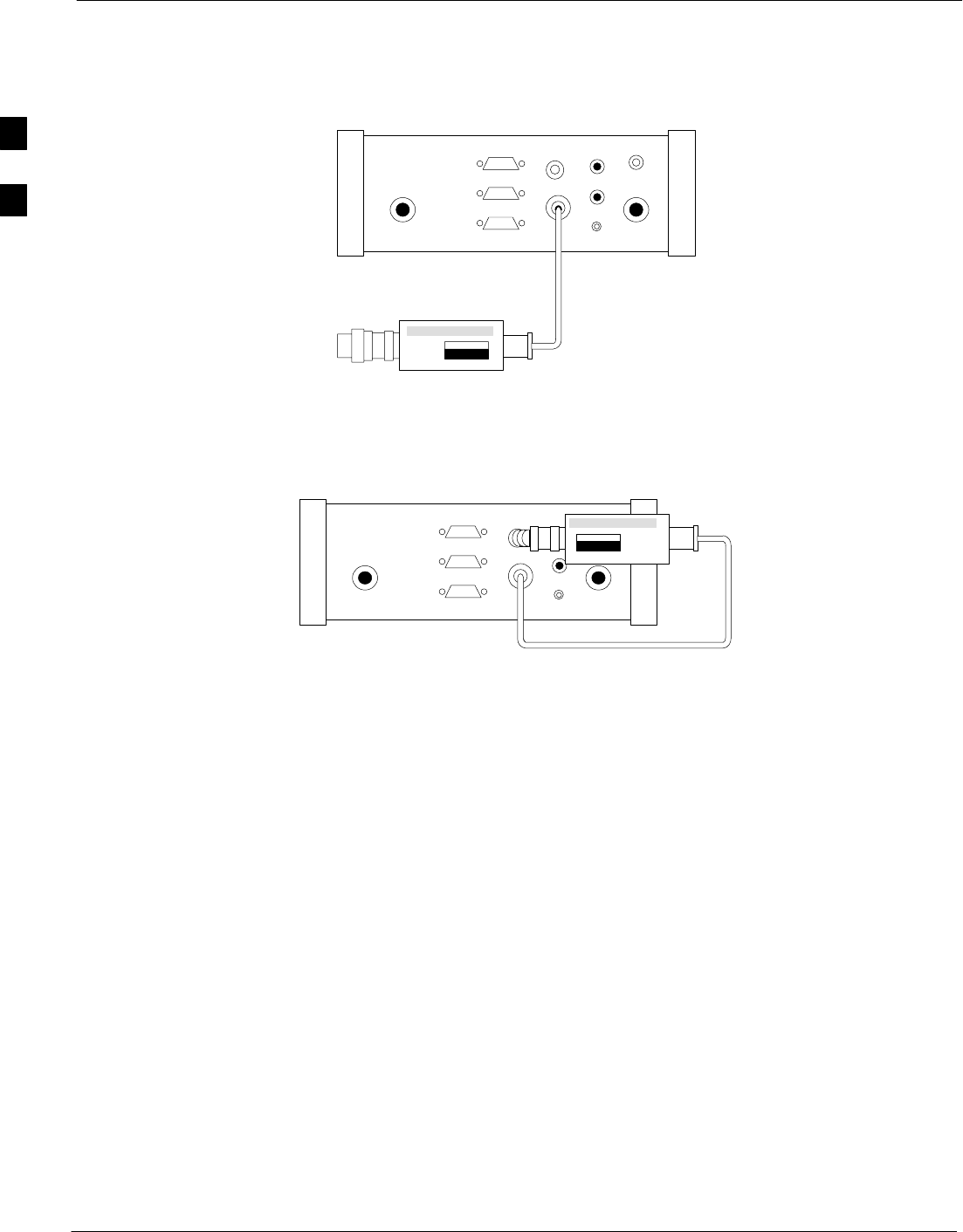
Test Equipment Preparation – continued
B-4 1X SC480 BTS Hardware Installation, Optimization/ATP, and FRU Jun 2004
DRAFT
Figure B-1: Agilent E7495A Pre–Power Sensor Calibration Connection
Use only
Agilent supplied
power adapter
GPS
GPIO
Serial 1
Serial 2
Power REF
50 MHz
Sensor
Ext Ref
In
Even Second
Sync In
Antenna
Port 1
RF Out / SWR
Port 2
RF In
POWER SENSOR
NOT CONNECTED
Figure B-2: Agilent E7495A Power Sensor Calibration Connection
Use only
Agilent supplied
power adapter
GPS
GPIO
Serial 1
Serial 2
Power REF
50 MHz
Sensor
Ext Ref
In
Even Second
Sync In
Antenna
Port 1
RF Out / SWR
Port 2
RF In
POWER SENSOR
CONNECTED
Cable Calibration
Follow the directions in the WinLMF program to calibrate cables.
– Calibrate the short cable (see Figure 6-12 or Figure 6-14) and two
10 dB pads to get a base line and then calibrate the TX and RX
setup. Since you need at least 40 dB of loss when doing the FER
test, the setup for RX is the same as TX.
ATP Setup
TX Path Calibration setup is shown in Test Equipment Setup (see
Figure 6-19 through Figure 6-22).
B
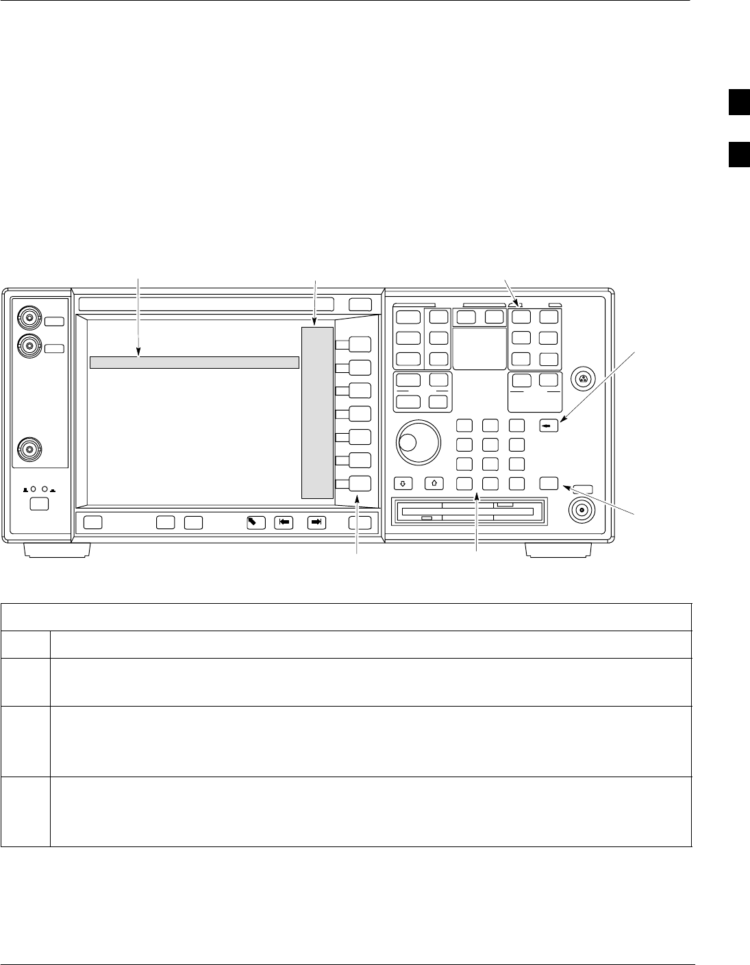
Verifying and Setting GPIB Addresses
Jun 2004 1X SC480 BTS Hardware Installation, Optimization/ATP, and FRU B-5
DRAFT
Agilent E4406A Transmitter
Tester GPIB Address
Refer to Figure B-3 and follow the procedure in Table B-4 to verify and,
if necessary, change the Agilent E4406A GPIB address.
Figure B-3: Setting Agilent E4406A GPIB Address
System Key
Bk Sp Key
Enter Key
Data Entry KeypadSoftkey Buttons
Softkey Label Display AreaActive Function Area
ti-CDMA-WP-00085-v01-ildoc-ftw
Table B-4: Verify and Change Agilent E4406A GPIB Address
Step Action
1In the SYSTEM section of the instrument front panel, press the System key.
– The softkey labels displayed on the right side of the instrument screen will change.
2Press the Config I/O softkey button to the right of the instrument screen.
– The softkey labels will change.
– The current instrument GPIB address will be displayed below the GPIB Address softkey label.
3If the current GPIB address is not set to 18, perform the following to change it:
3a Press the GPIB Address softkey button. In the on–screen Active Function Area, GPIB Address will
be displayed followed by the current GPIB address.
. . . continued on next page
B
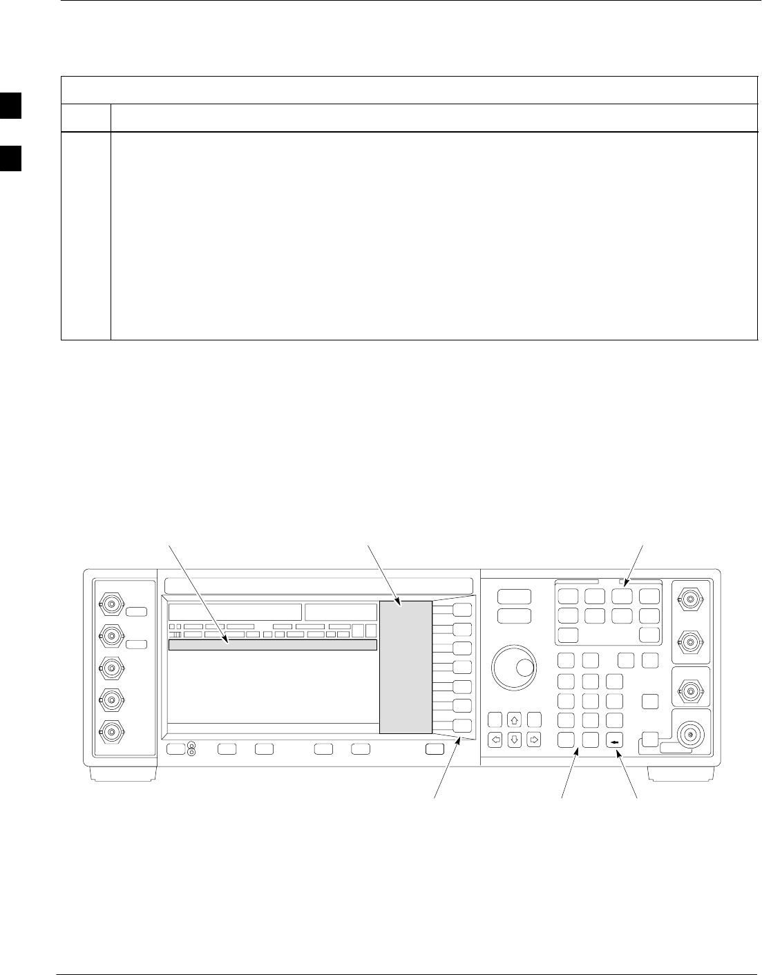
Verifying and Setting GPIB Addresses – continued
B-6 1X SC480 BTS Hardware Installation, Optimization/ATP, and FRU Jun 2004
DRAFT
Table B-4: Verify and Change Agilent E4406A GPIB Address
Step Action
3b On front panel Data Entry keypad, enter the communications system analyzer GPIB address of 18.
– The GPIB Address label will change to Enter.
– Characters typed with the keypad will replace the current GPIB address in the Active Function
Area.
NOTE
To correct an entry, press Bk Sp key to delete one character at a time.
3c Press the Enter softkey button or the keypad Enter key to set the new GPIB address.
– The Config I/O softkey labels will reappear.
– The new GPIB address will be displayed under the GPIB Address softkey label.
Agilent E4432B Signal
Generator GPIB Address
Refer to Figure B-4 and follow the procedure in Table B-5 to verify and,
if necessary, change the Agilent E4432B GPIB address.
Figure B-4: Setting Agilent E4432B GPIB Address
Numeric
Keypad
Softkey
Buttons
Softkey Label
Display Area
Active Entry
Area
Backspace
Key
Utility
Key
B

Verifying and Setting GPIB Addresses – continued
Jun 2004 1X SC480 BTS Hardware Installation, Optimization/ATP, and FRU B-7
DRAFT
Table B-5: Verify and Change Agilent E4432B GPIB Address
Step Action
1In the MENUS section of the instrument front panel, press the Utility key.
– The softkey labels displayed on the right side of the instrument screen will change.
2Press the GPIB/RS232 softkey button to the right of the instrument screen.
– The softkey labels will change.
– The current instrument GPIB address will be displayed below the GPIB Address softkey label.
3If the current GPIB address is not set to 1, perform the following to change it:
3a Press the GPIB Address softkey button.
– The GPIB Address label and current GPIB address will change to boldface.
– In the on–screen Active Entry Area, Address: will be displayed followed by the current GPIB
address.
3b On the front panel Numeric keypad, enter the signal generator GPIB address of 1.
– The GPIB Address label will change to Enter.
– Characters typed on the keypad will replace the current GPIB address in the Active Entry display.
NOTE
To correct an entry, press the backspace key at the lower right of the keypad to delete one character at
a time.
3c Press the Enter softkey button to set the new GPIB address.
– The new GPIB address will be displayed under the GPIB Address softkey label.
Advantest R3267 Spectrum
Analyzer GPIB Address
Refer to Figure B-5 and perform the procedure in Table B-6 to verify
and, if necessary, change the Advantest R3267 spectrum analyzer GPIB
address.
B
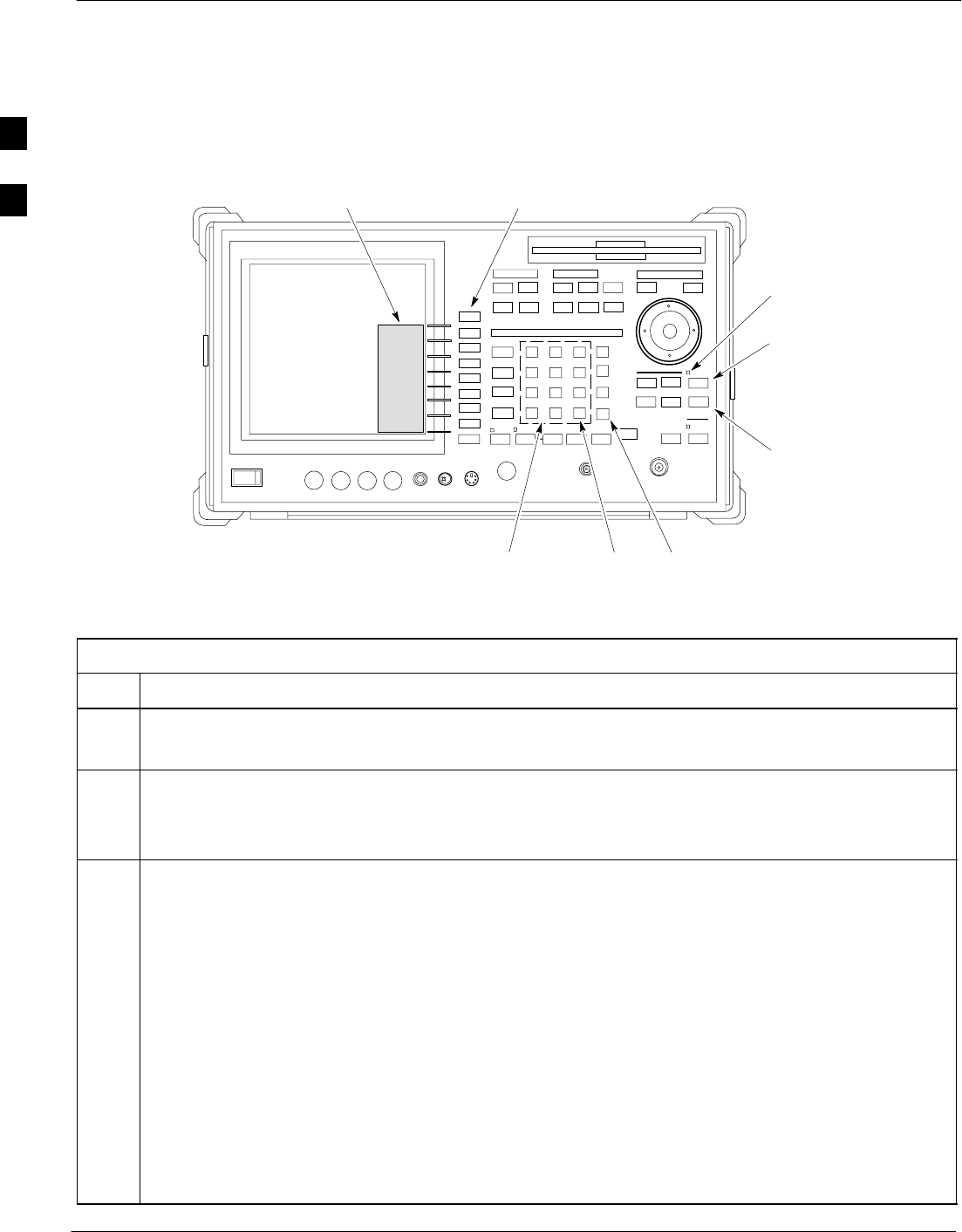
Verifying and Setting GPIB Addresses – continued
B-8 1X SC480 BTS Hardware Installation, Optimization/ATP, and FRU Jun 2004
DRAFT
Figure B-5: Setting Advantest R3267 GPIB Address
onREMOTE
LED
LCL Key
CONFIG
Key
Softkey Lable
Display Area Softkey
Buttons
Keypad BS
Key ENTR
Key
Table B-6: Verify and Change Advantest R3267 GPIB Address
Step Action
1If the REMOTE LED is lighted, press the LCL key.
– The LED extinguishes.
2Press the CONFIG key.
–CONFIG softkey labels will appear in the softkey label display area of the instrument display.
– The current GPIB address will be displayed below the GPIB Address softkey label.
3If the current GPIB address is not set to 18, perform the following to change it:
3a Press the GPIB Address softkey. A GPIB Address entry window will open in the instrument display
showing the current GPIB address.
3b Enter 18 on the keypad in the ENTRY section of the instrument front panel.
– Characters typed on the keypad will replace the address displayed in the GPIB Address entry
window.
NOTE
To correct an entry, press the BS (backspace) key at the lower right of the keypad to delete one
character at a time.
3c Press the ENTR key to the lower right of the keypad to set the new GPIB address.
– The GPIB Address entry window closes.
– The new address is displayed in the bottom portion of the GPIB Address softkey label.
B
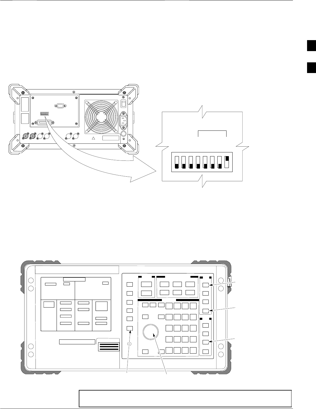
Verifying and Setting GPIB Addresses – continued
Jun 2004 1X SC480 BTS Hardware Installation, Optimization/ATP, and FRU B-9
DRAFT
Advantest R3562 Signal
Generator GPIB Address
Set the GP–IB ADDRESS switch on the rear of the Advantest R3562
signal generator to address 1 as shown in Figure B-6.
Figure B-6: Advantest R3562 GPIB Address Switch Setting
123 45678
54321
GP–IP ADDRESS
1
0
GPIB Address set to “1”
Agilent 8935 Series E6380
(formerly HP 8935) Test Set
GPIB Address
Refer to Figure B-7 and follow the procedure in Table B-7 to verify and,
if necessary, change the Agilent 8935 GPIB address.
Figure B-7: Agilent 8935 Test Set
Pre-
set
Cursor Control
Shift
Inst Con-
fig
Local
FW00885
NOTE This procedure assumes that the test equipment is set up and
ready for testing.
B

Verifying and Setting GPIB Addresses – continued
B-10 1X SC480 BTS Hardware Installation, Optimization/ATP, and FRU Jun 2004
DRAFT
Table B-7: Verify and/or Change Agilent 8935 (formerly HP 8935) GPIB Address
Step Action
1NOTE
The HP I/O configuration MUST be set to Talk & Listen, or no device on the GPIB will be
accessible. (Consult test equipment OEM documentation for additional information as required.)
To verify that the GPIB addresses are set correctly, press Shift and LOCAL on the Agilent 8935.
– The current HP–IB address is displayed at the top of the screen.
NOTE
HP–IB is the same as GPIB.
2If the current GPIB address is not set to 18, perform the following to change it:
2a – Press Shift and Inst Config.
2b – Turn the Cursor Control knob to move the cursor to the HP–IB Adrs field.
2c – Press the Cursor Control knob to select the field.
2d – Turn the Cursor Control knob as required to change the address to 18.
2e – Press the Cursor Control knob to set the address.
3 Press Preset to return to normal operation.
B
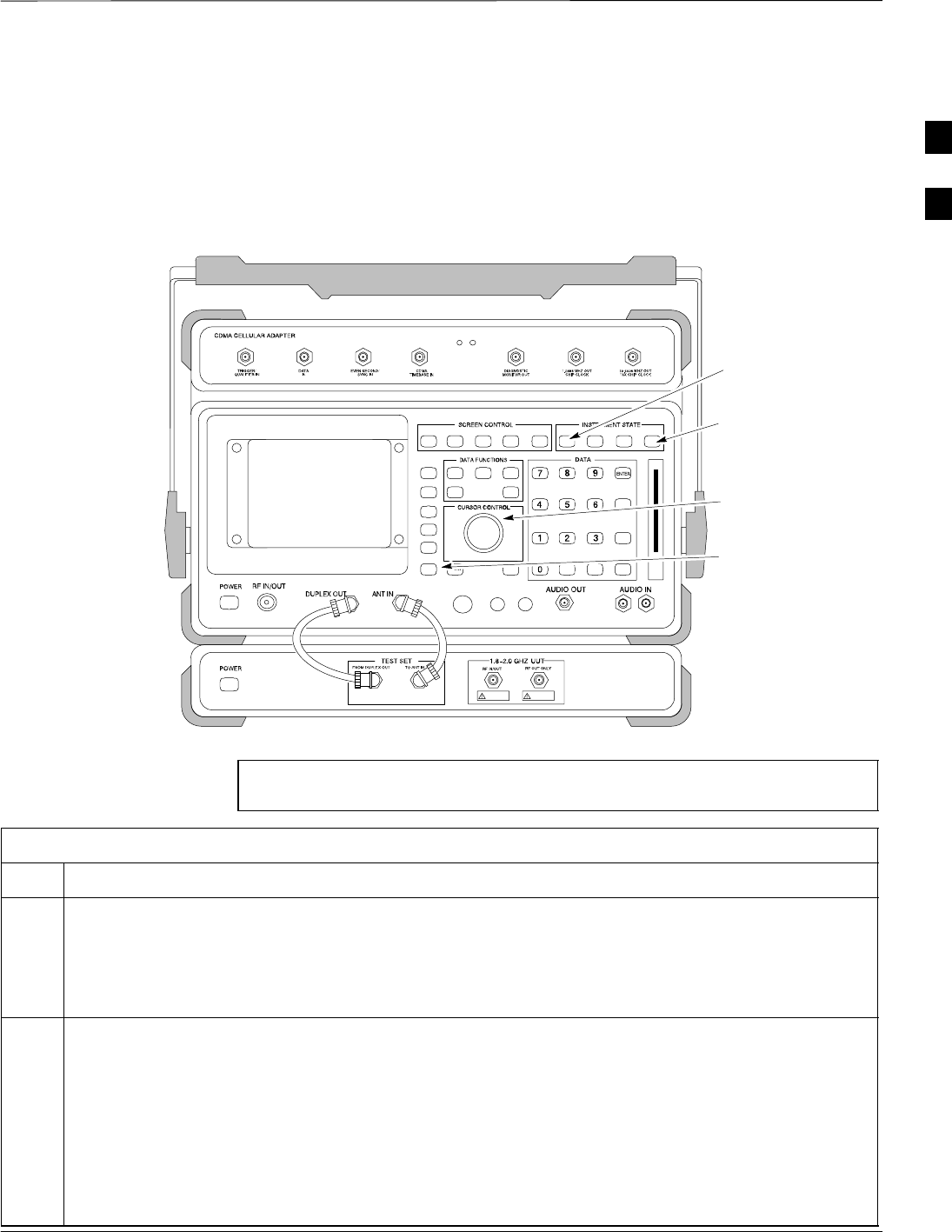
Verifying and Setting GPIB Addresses – continued
Jun 2004 1X SC480 BTS Hardware Installation, Optimization/ATP, and FRU B-11
DRAFT
Hewlett Packard HP8921A and
HP83236A/B GPIB Address
Refer to Figure B-8 and follow the procedure in Table B-8 to verify and,
if necessary, change the HP 8921A HP 83236A GPIB addresses.
Figure B-8: HP 8921A and HP 83236A/B
Preset
Cursor Control
Shift
Local
NOTE This procedure assumes that the test equipment is set up and
ready for testing.
Table B-8: Verify and/or Change HP 8921A and HP 83236A GPIB Addresses
Step Action
1To verify that the GPIB addresses are set correctly, press Shift and LOCAL on the HP 8921A.
– The current HP–IB address is displayed at the top of the screen.
NOTE
HP–IB is the same as GPIB.
2If the current HP–IB address is not set to 18, perform the following to change it:
2a – Turn the Cursor Control knob to move the cursor to More and press the knob to select the field.
2b – Turn the Cursor Control knob to move the cursor to I/O Config and press the knob to select the
field.
2c – Turn the Cursor Control knob to move the cursor to Adrs and press the knob to select the field.
2d – Turn the Cursor Control knob to change the HP–IB address to 18 and press the knob to set the
address.
B
Verifying and Setting GPIB Addresses – continued
B-12 1X SC480 BTS Hardware Installation, Optimization/ATP, and FRU Jun 2004
DRAFT
Table B-8: Verify and/or Change HP 8921A and HP 83236A GPIB Addresses
Step Action
2e – Press Shift and Preset to return to normal operation.
3To set the HP 83236A (or B) PCS Interface GPIB address=19, set the DIP switches as follows:
– A1=1, A2=1, A3=0, A4=0, A5=1, HP–IB/Ser = 1
Advantest R3465
Communications Test Set GPIB
Address
Refer to Figure B-9 and follow the procedure in Table B-9 to verify and,
if necessary, change the GPIB address for the Advantest R3465.
Figure B-9: R3465 Communications Test Set
BNC
“T”
REF UNLOCK EVEN
SEC/SYNC IN CDMA
TIME BASE IN
POWER
OFF ON
REF FW00337
LCL Shift Preset
GPIB and others
Vernier
Knob
NOTE This procedure assumes that the test equipment is set up and
ready for testing.
Table B-9: Verify and/or Change Advantest R3465 GPIB Address
Step Action
1To verify that the GPIB address is set correctly, perform the following:
1a – Press SHIFT then PRESET.
1b – Press LCL.
1c – Press the GPIB and Others CRT menu key to view the current address.
2If the current GPIB address is not set to 18, perform the following to change it:
2a – Turn the vernier knob as required to select 18.
B

Verifying and Setting GPIB Addresses – continued
Jun 2004 1X SC480 BTS Hardware Installation, Optimization/ATP, and FRU B-13
DRAFT
Table B-9: Verify and/or Change Advantest R3465 GPIB Address
Step Action
2b – Press the vernier knob to set the address.
3To return to normal operation, press Shift and Preset.
Motorola CyberTest GPIB
Address
Follow the steps in Table B-10 to verify and, if necessary, change the
GPIB address on the Motorola CyberTest. Changing the GPIB address
requires the following items:
SMotorola CyberTest communications analyzer.
SComputer running Windows 3.1/Windows 95.
SMotorola CyberTAME software program “TAME”.
SParallel printer port cable (shipped with CyberTest).
NOTE This procedure assumes that the test equipment is set up and
ready for testing.
Table B-10: Verify and/or Change Motorola CyberTest GPIB Address
Step Action
1On the LMF desktop, locate the CyberTAME icon. Double click on the icon to run the CyberTAME
application.
2In the CyberTAME window taskbar, under Special, select IEEE.488.2.
3CyberTAME software will query the CyberTest Analyzer for its current GPIB address. It then will
open the IEEE 488.2 dialog box. If the current GPIB address is not 18, perform the following
procedure to change it:
3a Use the up or down increment arrows or double–click in the field and type the number to set the
address to 18.
3b Click on the OK button. The new address will be written to the CyberTest through the parallel port
and saved.
4Verify that the address has been set by repeating steps 2 and 3. The new address should now appear in
the IEEE 488.2 dialog box Address field.
B
Verifying and Setting GPIB Addresses – continued
B-14 1X SC480 BTS Hardware Installation, Optimization/ATP, and FRU Jun 2004
DRAFT
HP 437 Power Meter GPIB
Address
Refer to Figure B-10 and follow the steps in Table B-11 to verify and, if
necessary, change the HP 437 GPIB address.
Figure B-10: HP 437 Power Meter
ENTER
PRESET
SHIFT (BLUE) PUSHBUTTON –
ACCESSES FUNCTION AND
DATA ENTRY KEYS IDENTIFIED
WITH LIGHT BLUE TEXT ON
THE FRONT PANEL ABOVE
THE BUTTONS
FW00308REF
NOTE This procedure assumes that the test equipment is set up and
ready for testing.
Table B-11: Verify and/or Change HP 437 Power Meter GPIB Address
Step Action
1 Press Shift and PRESET.
2Use the y arrow key to navigate to HP–IB ADRS and press ENTER.
The HP–IB address is displayed.
NOTE
HP–IB is the same as GPIB.
3If the current GPIB address is not set to 13, perform the following to change it:
– Use the y b arrow keys to change the HP–IB ADRS to 13.
– Press ENTER to set the address.
4 Press Shift and ENTER to return to a standard configuration.
B

Verifying and Setting GPIB Addresses – continued
Jun 2004 1X SC480 BTS Hardware Installation, Optimization/ATP, and FRU B-15
DRAFT
Gigatronics 8541C Power
Meter GPIB Address
Refer to Figure B-11 and follow the steps in Table B-12 to verify and, if
necessary, change the Gigatronics 8541C power meter GPIB address.
Figure B-11: Gigatronics 8541C Power Meter Detail
NOTE This procedure assumes that the test equipment is set up and
ready for testing.
Table B-12: Verify and/or Change Gigatronics 8541C Power Meter GPIB Address
Step Action
1! CAUTION
Do not connect/disconnect the power meter sensor cable with AC power applied to the meter.
Disconnection could result in destruction of the sensing element or miscalibration.
Press MENU.
2Use the b arrow key to select CONFIG MENU and press ENTER.
3Use the b arrow key to select GPIB and press ENTER.
The current Mode and GPIB Address are displayed.
4If the Mode is not set to 8541C, perform the following to change it:
Use the a ’ arrow keys as required to select MODE.
Use the by arrow keys as required to set MODE to 8541C.
5If the GPIB address is not set to 13, perform the following to change it:
Use the ’ arrow key to select ADDRESS.
Use the by arrow keys as required to set the GPIB address to 13.
6 Press ENTER to return to normal operation.
B
Verifying and Setting GPIB Addresses – continued
B-16 1X SC480 BTS Hardware Installation, Optimization/ATP, and FRU Jun 2004
DRAFT
RS232 GPIB Interface Adapter
Be sure that the RS–232 GPIB interface adapter DIP switches are set as
shown in Figure B-12.
Figure B-12: RS232 GPIB Interface Adapter
RS232–GPIB
INTERFACE BOX
S MODE
DATA FORMAT
BAUD RATE
GPIB ADRS
ON
DIP SWITCH SETTINGS
G MODE
B

Test Equipment Connection, Testing, and Control
Jun 2004 1X SC480 BTS Hardware Installation, Optimization/ATP, and FRU B-17
DRAFT
Inter–unit Connection, Testing,
and Control Settings
The following illustrations, tables, and procedures provide the
information necessary to prepare various items of CDMA test equipment
supported by the WinLMF for BTS calibration and/or acceptance testing.
HP 8921A with PCS Interface
Test Equipment Connections
The following diagram depicts the rear panels of the HP 8921A test
equipment as configured to perform automatic tests. All test equipment
is controlled by the WinLMF via an IEEE–488/GPIB bus. The WinLMF
expects each piece of test equipment to have a factory-set GPIB address
(refer to Table B-8 and Figure B-8). If there is a communications
problem between the WinLMF and any piece of test equipment, verify
that the GPIB addresses have been set correctly and that the GPIB cables
are firmly connected to the test equipment.
Table B-13 shows the connections when not using an external 10 MHz
Rubidium reference.
Table B-13: HP 8921A/600 Communications Test Set Rear Panel Connections Without Rubidium Reference
From Test Set: To Interface:
Connector Type
8921A 83203B CDMA 83236A PCS
Connector Type
CW RF OUT CW RF IN SMC–female – SMC–female
114.3 MHZ IF OUT 114.3 MHZ IF IN SMC–female – SMC–female
IQ RF IN IQ RF OUT SMC–female – SMC–female
DET OUT AUX DSP IN SMC–female – SMC–female
CONTROL I/O CONTROL I/O 45–pin custom BUS
10 MHZ OUT SYNTH REF IN BNC–male – BNC–male
HPIB INTERFACE HPIB INTERFACE HPIB cable
10 MHZ OUT REF IN BNC–male – BNC–male
B
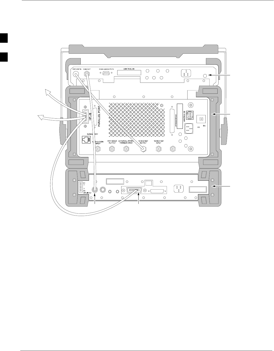
Test Equipment Connection, Testing, and Control – continued
B-18 1X SC480 BTS Hardware Installation, Optimization/ATP, and FRU Jun 2004
DRAFT
REAR PANEL
COMMUNICATIONS TEST SET
REF IN
HP 83203B CDMA
CELLULAR ADAPTER
HP 8921A CELL
SITE TEST SET
HP 83236A PCS
INTERFACE
HP–IB
TO GPIB
INTERFACE
BOX
TO POWER
METER GPIB
CONNECTOR
FW00368
Figure B-13: HP 8921A/600 Cable Connections for 10 MHz Signal and GPIB
without Rubidium Reference
B

Test Equipment Connection, Testing, and Control – continued
Jun 2004 1X SC480 BTS Hardware Installation, Optimization/ATP, and FRU B-19
DRAFT
Figure B-14 shows the connections when using an external 10 MHz
Rubidium reference.
Table B-14: HP 8921A/600 Communications Test Set Rear Panel Connections With Rubidium Reference
From Test Set: To Interface:
Connector Type
8921A 83203B CDMA 83236A PCS
Connector Type
CW RF OUT CW RF IN SMC–female – SMC–female
114.3 MHZ IF OUT 114.3 MHZ IF IN SMC–female – SMC–female
IQ RF IN IQ RF OUT SMC–female – SMC–female
DET OUT AUX DSP IN SMC–female – SMC–female
CONTROL I/O CONTROL I/O 45–pin custom BUS
10 MHZ OUT REF IN BNC–male – BNC–male
HPIB INTERFACE HPIB INTERFACE HPIB cable
10 MHZ INPUT 10 MHZ OUT BNC–male – BNC–male
B
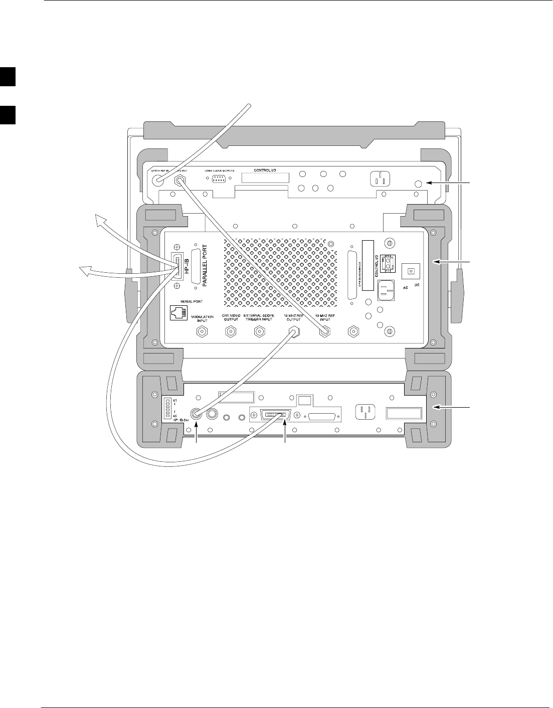
Test Equipment Connection, Testing, and Control – continued
B-20 1X SC480 BTS Hardware Installation, Optimization/ATP, and FRU Jun 2004
DRAFT
REF IN
REAR PANEL
COMMUNICATIONS TEST SET
TO POWER
METER GPIB
CONNECTOR
TO GPIB
INTERFACE
BOX
10 MHZ WITH
RUBIDIUM STANDARD
HP 83203B CDMA
CELLULAR ADAPTER
HP 8921A CELL
SITE TEST SET
HP 83236A PCS
INTERFACE
HP–IB
FW00369
Figure B-14: HP 8921A Cable Connections for 10 MHz Signal and GPIB with Rubidium Reference
B

Test Equipment Connection, Testing, and Control – continued
Jun 2004 1X SC480 BTS Hardware Installation, Optimization/ATP, and FRU B-21
DRAFT
HP 8921A with PCS Interface
System Connectivity Test
Follow the steps outlined in Table B-15 to verify that the connections
between the PCS Interface and the HP 8921A are correct and cables are
intact. The software also performs basic functionality checks of each
instrument.
Disconnect other GPIB devices, especially system
controllers, from the system before running the
connectivity software.
NOTE
Table B-15: System Connectivity
Step Action
NOTE
– Perform this procedure after test equipment has been allowed to warm–up and stabilize for a
minimum of 60 minutes.
1Insert HP 83236A Manual Control/System card into memory card slot.
2Press the [PRESET] pushbutton.
3Press the Screen Control [TESTS] pushbutton to display the “Tests” Main Menu screen.
4Position the cursor at Select Procedure Location and select it by pressing the cursor control knob. In
the Choices selection box, select Card.
5Position the cursor at Select Procedure Filename and select it by pressing the cursor control knob. In
the Choices selection box, select SYS_CONN.
6Position the cursor at RUN TEST and select it. The software will provide operator prompts through
completion of the connectivity setup.
7Do the following when the test is complete,
Sposition cursor on STOP TEST and select it
SOR press the [K5] pushbutton.
8To return to the main menu, press the [K5] pushbutton.
9Press the [PRESET] pushbutton.
Pretest Setup for HP 8921A
Before the HP 8921A CDMA analyzer is used for WinLMF–controlled
testing it must be set up correctly for automatic testing. Perform the
procedure in Table B-16.
B

Test Equipment Connection, Testing, and Control – continued
B-22 1X SC480 BTS Hardware Installation, Optimization/ATP, and FRU Jun 2004
DRAFT
Table B-16: Pretest Setup for HP 8921A
Step Action
1Unplug the memory card if it is plugged in.
2Press the CURSOR CONTROL knob.
3Position the cursor at IO CONFIG (under To Screen and More) and select it.
4Select Mode and set for Talk&Lstn.
Pretest Setup for Agilent 8935
Before the Agilent 8935 analyzer is used for WinLMF controlled testing
it must be set up correctly for automatic testing. Perform the procedure
in Table B-17.
Table B-17: Pretest Setup for Agilent 8935
Step Action
1Unplug the memory card if it is plugged in.
2Press the Shift button and then press the I/O Config button.
3Press the Push to Select knob.
4Position the cursor at IO CONFIG and select it.
5 Select Mode and set for Talk&Lstn.
Advantest R3465 Connection
The following diagram depicts the rear panels of the Advantest R3465
test equipment as configured to perform automatic tests. All test
equipment is controlled by the WinLMF via an IEEE–488/GPIB bus.
The WinLMF expects each piece of test equipment to have a factory-set
GPIB address (refer to Table B-9 and Figure B-9). If there is a
communications problem between the WinLMF and any piece of test
equipment, verify that the GPIB addresses have been set correctly and
that the GPIB cables are firmly connected to the test equipment.
Figure B-15 shows the connections when not using an external 10 MHz
Rubidium reference.
B
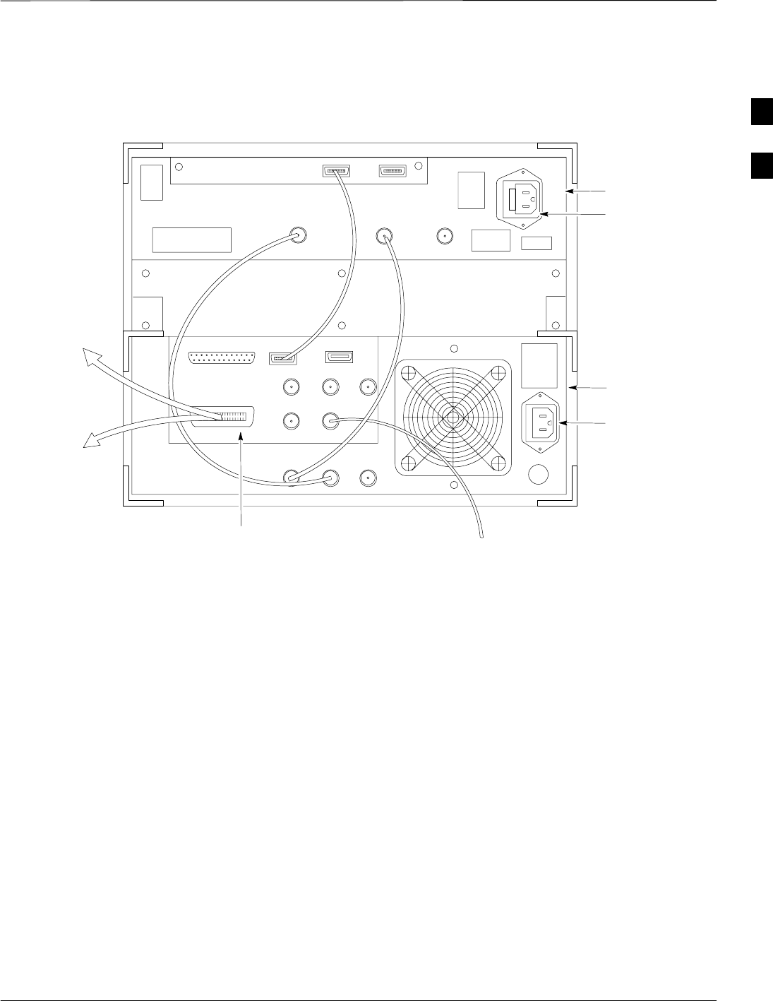
Test Equipment Connection, Testing, and Control – continued
Jun 2004 1X SC480 BTS Hardware Installation, Optimization/ATP, and FRU B-23
DRAFT
ADVANTEST R3465
REAR PANEL
GPIB
CONNECTOR
SERIAL I/O
LOCAL IN
SERIAL I/O
SYN REF IN 10 MHZ OUT
PARALLEL
EXT TRIGGER
10 MHZ REF
GATE IN
GPIB
CDMA CLOCK OUT
AC POWER
AC POWER
R3561L
REAR PANEL
R3465
REAR PANEL
TO T–CONNECTOR
ON FRONT PANEL
(EVEN/SEC/SYNC IN)
XYZ
IF OUT
421 MHZ
TO POWER METER
GPIB CONNECTOR
TO GPIB
INTERFACE BOX
FW00370
Figure B-15: Cable Connections for Test Set without 10 MHz Rubidium Reference
B
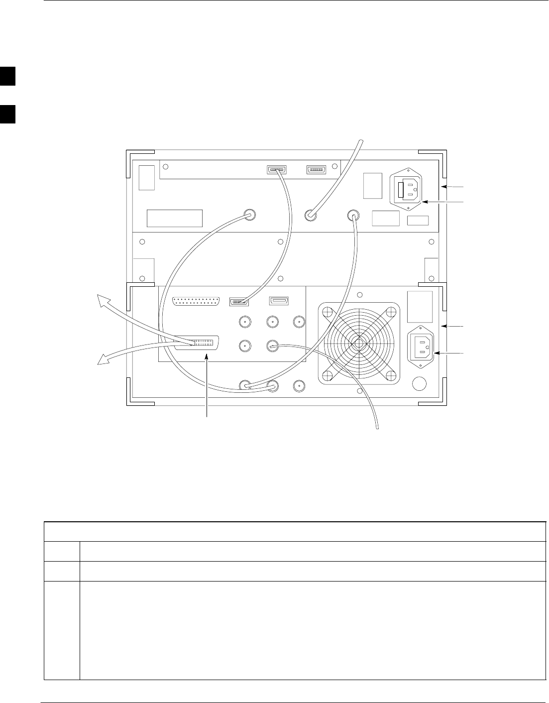
Test Equipment Connection, Testing, and Control – continued
B-24 1X SC480 BTS Hardware Installation, Optimization/ATP, and FRU Jun 2004
DRAFT
Figure B-16 shows the connections when using an external 10 MHz
Rubidium reference.
SERIAL I/O
GPIB
CONNECTOR ADVANTEST R3465
REAR PANEL
FROM 10 MHZ
RUBIDIUM REFERENCE
LOCAL IN
SERIAL I/O
IF OUT
SYN REF IN 10 MHZ OUT
PARALLEL
EXT TRIGGER
10 MHZ REF
GATE IN
GPIB
CDMA CLOCK OUT
AC POWER
AC POWER
R3465/3463
REAR PANEL
R3561L
REAR PANEL
TO T–CONNECTOR
ON FRONT PANEL
(EVEN SEC/SYNC IN)
XYZ
421 MHZ
TO POWER METER
GPIB CONNECTOR
TO GPIB
INTERFACE BOX
FW00371
Figure B-16: Cable Connections for Test Set with 10 MHz Rubidium Reference
R3465 GPIB Clock Set–up
Table B-18 describes the steps to set the clock for the Advantest R3465
equipment.
Table B-18: Advantest R3465 Clock Setup
Step Action
1Observe the current date and time displayed in upper right of the CRT display.
2If the date and time are incorrect, perform the following to change them:
2a – Push the Date/Time CRT menu key.
2b – Rotate the vernier knob to select and set.
2c – Push the vernier knob to enter.
2d – Push the SHIFT then PRESET pushbutton (just below the CRT display).
B

Test Equipment Connection, Testing, and Control – continued
Jun 2004 1X SC480 BTS Hardware Installation, Optimization/ATP, and FRU B-25
DRAFT
Pretest Setup for Advantest
R3465
Before the Advantest R3465 analyzer is used for WinLMF–controlled
testing it must be set up correctly for automatic testing. Perform the
procedure in Table B-19.
Table B-19: Pretest Setup for Advantest R3465
Step Action
1Press the SHIFT button so the LED next to it is illuminated.
2Press the RESET button.
Agilent 8932/E4432B Test
Equipment Interconnection
To perform FER testing on a 1X BTS with the Agilent 8935, a
1X–capable signal generator, such as the Agilent E4432B, must be used
in conjunction with the CDMA base station test set. For proper
operation, the test equipment items must be interconnected as follows:
10 MHz reference signal – Connect a BNC (M)–BNC (M) cable from
the 8935 10 MHz REF OUT connector to the E4432B 10MHz IN
connector as shown in Figure B-17
Even second pulse reference – Refer to Figure B-17, and connect a
BNC “T” connector to the 8935 EVEN SEC SYNC IN connector.
Connect a BNC (M)–BNC (M) cable from one side of the BNC “T” to
the E4432B PATTERN TRIG IN connector. Connect the other side of
the BNC “T” to the CSA Card SYNC MONITOR connector using a
BNC (M)–BNC (M) cable.
B
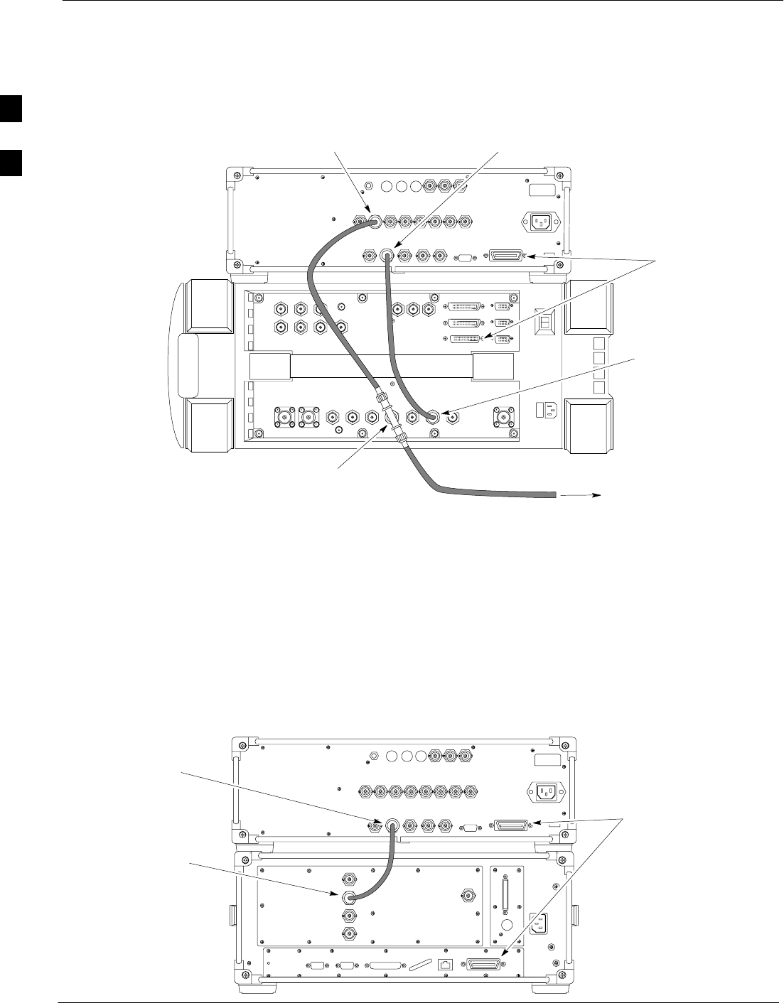
Test Equipment Connection, Testing, and Control – continued
B-26 1X SC480 BTS Hardware Installation, Optimization/ATP, and FRU Jun 2004
DRAFT
E4432B
10 MHz IN
TO GPIB
E4432B
PATTERN TRIG IN
TO CSA CARD
SYNC MONITOR
(EVEN SEC TICK)
8935
10 MHz
REF OUT
8935
EVEN SECOND
SYNC IN
WITH BNC “T” TDME0011–1
Figure B-17: Agilent 8935/E4432B 10MHz Reference and Even Second Tick Connections
Agilent E4406A/E4432B Test
Equipment Interconnection
To provide proper operation during testing when both units are required,
the 10 MHz reference signal from the E4406A transmitter test set must
be provided to the E4432B signal generator. Connect a BNC (M)–BNC
(M) cable from the E4406A 10 MHz OUT (SWITCHED) connector to
the E4432B 10MHz IN connector as shown in Figure B-18.
E4406A
10 MHz OUT
(SWITCHED)
E4432B
10 MHz IN
TO GPIB BOX
TDME0009–1
Figure B-18: Agilent 10 MHz Reference Connections
B
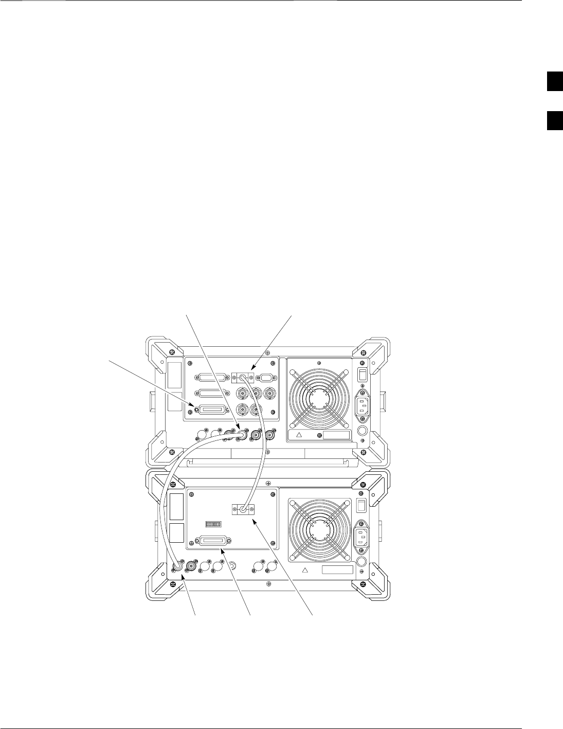
Test Equipment Connection, Testing, and Control – continued
Jun 2004 1X SC480 BTS Hardware Installation, Optimization/ATP, and FRU B-27
DRAFT
Advantest R3267/R3562 Test
Equipment Interconnection
To provide proper operation during testing when both units are required,
the R3257 spectrum analyzer must be interconnected with the R3562
signal generator as follows:
10 MHz reference signal – Connect a BNC (M)–BNC (M) cable
between the R3562 SYNTHE REF IN connector and the R3267 10
MHz OUT connector as shown in Figure B-19.
Serial I/O – Using the Advantest cable provided, connect the R3267
SERIAL I/O connector to the R3562 SERIAL I/O connector as shown
in Figure B-19.
TDME0010–1
R3562
SYNTHE REF IN TO GPIB
BOX R3562
SERIAL I/O
TO GPIB BOX
R3267
10 MHZ OUT R3267
SERIAL I/O
Figure B-19: Advantest 10 MHz Reference and Serial I/O Connections
B
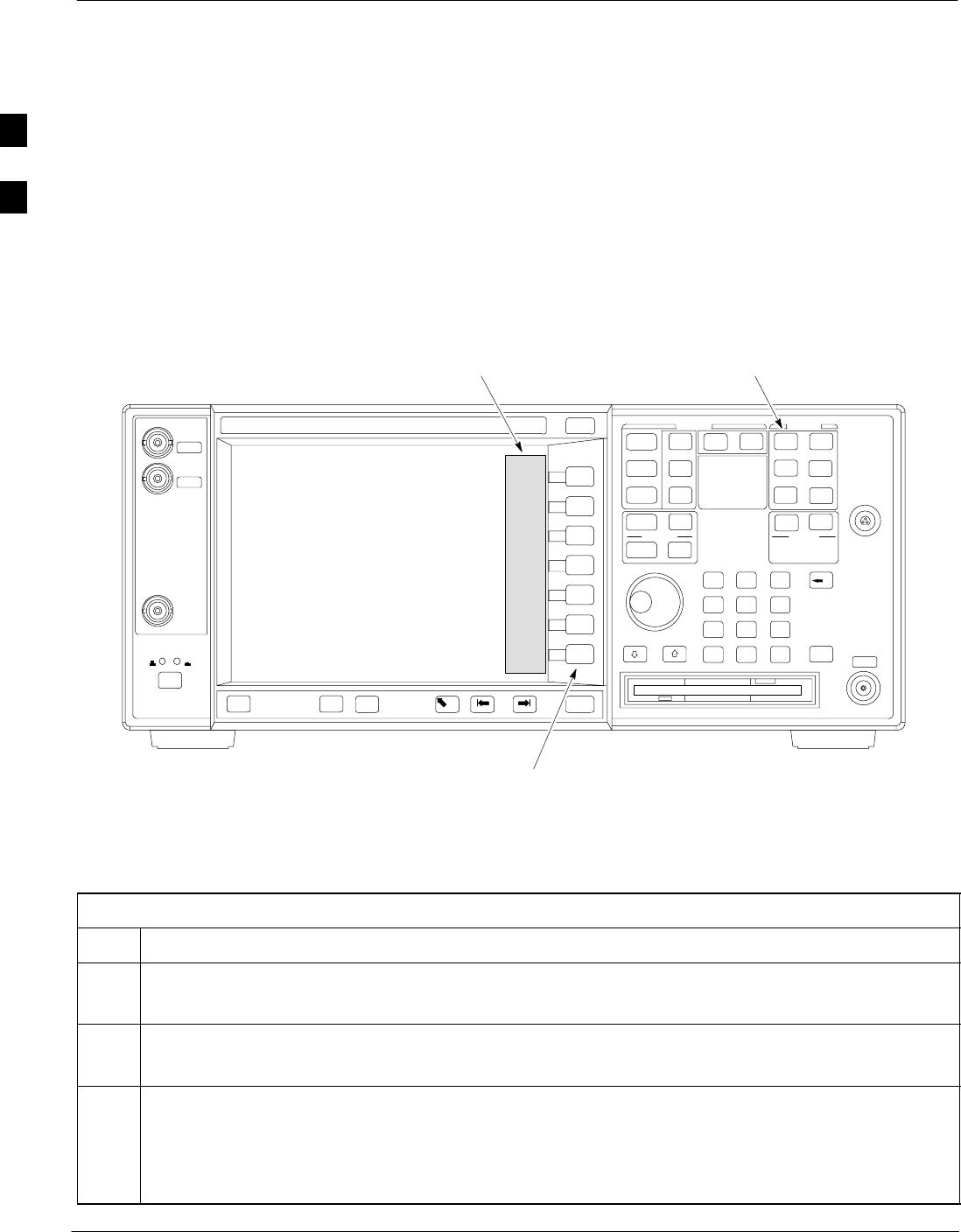
Equipment Calibration
B-28 1X SC480 BTS Hardware Installation, Optimization/ATP, and FRU Jun 2004
DRAFT
Calibration Without the LMF
Several test equipment items used in the optimization process require
pre–calibration actions or calibration verification which are not
supported by the LMF. Procedures to perform these activities for the
applicable test equipment items are covered in this section.
Agilent E4406A Transmitter
Tester Self–alignment
(Calibration)
System
Key
Softkey
Buttons
Softkey Label
Display Area
Figure B-20: Performing Agilent E4406A
Self–alignment (Calibration)
Refer to Figure B-20 and follow the procedure in Table B-20 to perform
the Agilent E4406A self–alignment (calibration).
Table B-20: Perform Agilent E4406A Self–alignment (Calibration)
Step Action
1In the SYSTEM section of the instrument front panel, press the System key.
– The softkey labels displayed on the right side of the instrument screen will change.
2Press the Alignments softkey button to the right of the instrument screen.
– The softkey labels will change.
3Press the Align All Now softkey button.
– All other instrument functions will be suspended during the alignment.
– The display will change to show progress and results of the alignments performed.
– The alignment will take less than one minute.
B
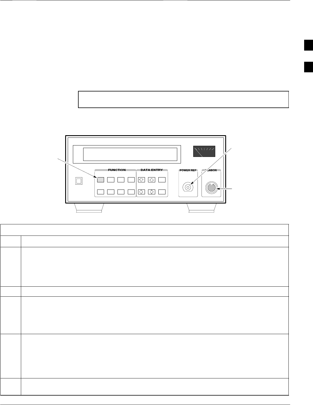
Equipment Calibration – continued
Jun 2004 1X SC480 BTS Hardware Installation, Optimization/ATP, and FRU B-29
DRAFT
Calibrating HP 437 Power
Meter
Precise transmit output power calibration measurements are made using
a bolometer–type broadband power meter with a sensitive power sensor.
Follow the steps outlined in Table B-21 to enter information unique to
the power sensor before calibrating the test setup. Refer to Figure B-21
as required.
NOTE This procedure must be done before the automated calibration to
enter power sensor specific calibration values.
Figure B-21: Power Meter Detail
CONNECT POWER
SENSOR WITH POWER
METER TURNED OFF
CONNECT POWER SENSOR
TO POWER REFERENCE
WHEN CALIBRATING UNIT.
POWER REFERENCE IS
ENABLED USING THE SHIFT ’
KEYS
SHIFT (BLUE) PUSHBUTTON –
ACCESSES FUNCTION AND
DATA ENTRY KEYS IDENTIFIED
WITH LIGHT BLUE TEXT ON
THE FRONT PANEL ABOVE
THE BUTTONS
FW00308
Table B-21: HP 437 Power Meter Calibration Procedure
Step Action
1! CAUTION
Do not connect/disconnect the power meter sensor cable with AC power applied to the meter.
Disconnection could result in destruction of the sensing element or mis–calibration.
Make sure the power meter AC LINE pushbutton is OFF.
2Connect the power sensor cable to the SENSOR input.
3Set the AC LINE pushbutton to ON.
NOTE
The calibration should be performed only after the power meter and sensor have been allowed to
warm–up and stabilize for a minimum of 60 minutes.
4Perform the following to set or verify the correct power sensor model:
4a – Press [SHIFT] then [a] to select SENSOR.
4b – Identify the power sensor model number from the sensor label.
4c – Use the [y] or [b] button to select the appropriate model; then press [ENTER].
5Refer to the illustration for step 8, and perform the following to ensure the power reference output is
OFF:
. . . continued on next page
B
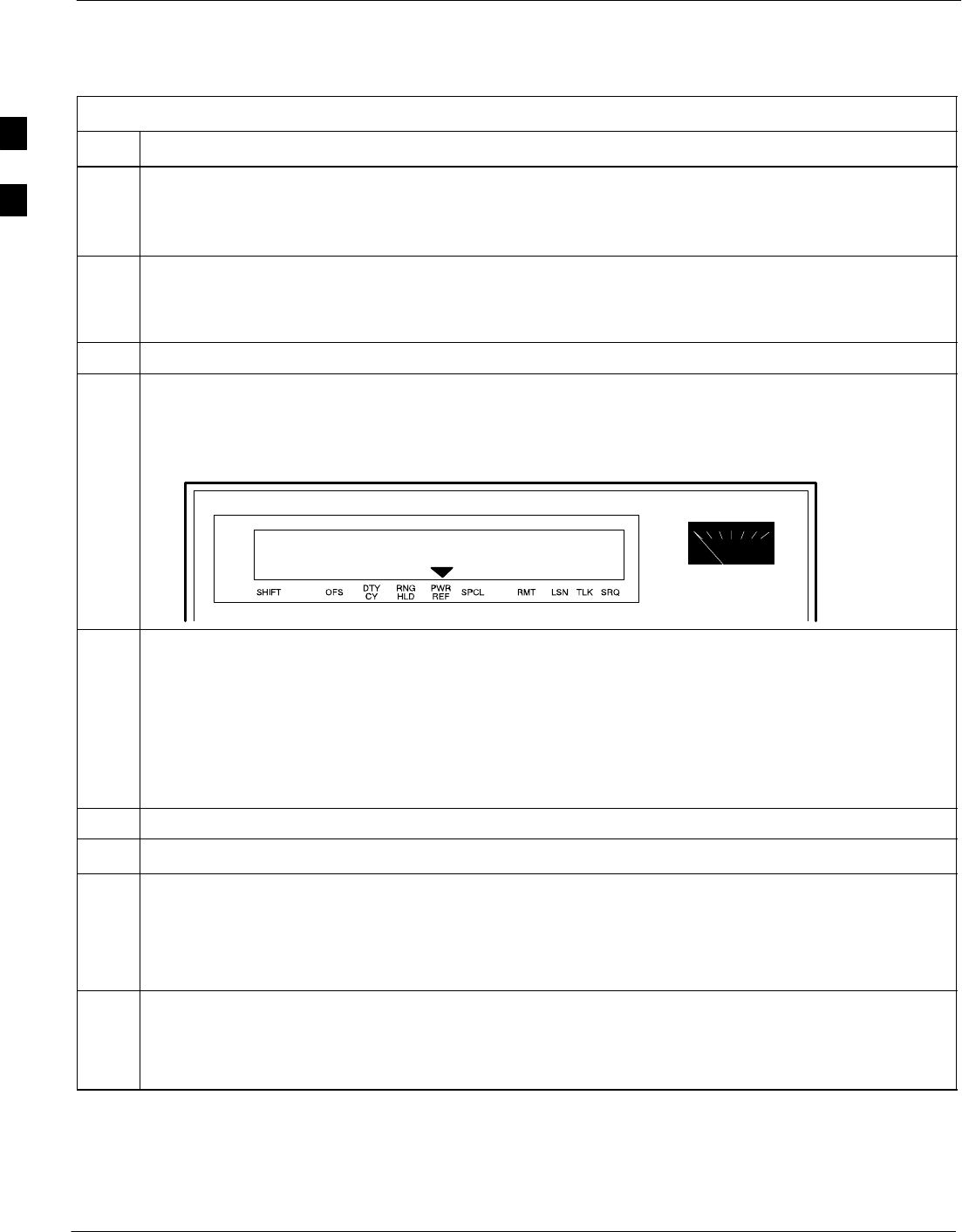
Equipment Calibration – continued
B-30 1X SC480 BTS Hardware Installation, Optimization/ATP, and FRU Jun 2004
DRAFT
Table B-21: HP 437 Power Meter Calibration Procedure
Step Action
5a – Observe the instrument display and determine if the triangular indicator over PWR REF is
displayed.
5b – If the triangular indicator is displayed, press [SHIFT] then [’] to turn it off.
6 Press [ZERO].
– Display will show “Zeroing ******.”
– Wait for process to complete.
7Connect the power sensor to the POWER REF output.
8Turn on the PWR REF by performing the following:
8a – Press [SHIFT] then [’].
8b – Verify that the triangular indicator (below) appears in the display above PWR REF.
9Perform the following to set the REF CF%:
9a – Press ([SHIFT] then [ZERO]) for CAL.
9b – Enter the sensor’s REF CF% from the sensor’s decal using the arrow keys and press [ENTER].
(The power meter will display ”CAL *****” for a few seconds.)
NOTE
If the REF CAL FACTOR (REF CF) is not shown on the power sensor, assume it to be 100%.
10 Perform the following to set the CAL FAC %:
10a – Press [SHIFT] then [FREQ] for CAL FAC.
10b – On the sensor’s decal, locate an approximate calibration percentage factor (CF%) at 2 GHz.
10c – Enter the sensor’s calibration % (CF%) using the arrow keys and press [ENTER].
–– When complete, the power meter will typically display 0.05 dBm. (Any reading between
0.00 and 0.10 is normal.)
11 To turn off the PWR REF, perform the following:
11a – Press [SHIFT] then [’].
11b – Disconnect the power sensor from the POWER REF output.
B

Equipment Calibration – continued
Jun 2004 1X SC480 BTS Hardware Installation, Optimization/ATP, and FRU B-31
DRAFT
Calibrating Gigatronics 8541C
Power Meter
Precise transmit output power calibration measurements are made using
a bolometer–type broadband power meter with a sensitive power sensor.
Follow the steps in Table B-22 to enter information unique to the power
sensor.
Table B-22: Calibrate Gigatronics 8541C Power Meter
Step Action
1! CAUTION
Do not connect/disconnect the power meter sensor cable with AC power applied to the meter.
Disconnection could result in destruction of the sensing element or miscalibration.
Make sure the power meter POWER pushbutton is OFF.
2Connect the power sensor cable to the SENSOR input.
3Set the POWER pushbutton to ON.
NOTE
Allow the power meter and sensor to warm up and stabilize for a minimum of 60 minutes before
performing the calibration procedure.
4Connect the power sensor to the CALIBRATOR output connector.
5 Press ZERO.
– Wait for the process to complete. Sensor factory calibration data is read to power meter during this
process.
6When the zeroing process is complete, disconnect the power sensor from the CALIBRATOR output.
Figure B-22: Gigatronics 8541C Power Meter Detail
CONNECT POWER SENSOR
WITH POWER METER
TURNED OFF
CONNECT POWER SENSOR TO
CALIBRATOR POWER REFERENCE
WHEN CALIBRATING/ZEROING UNIT
FRONT View REAR View
GPIB CONNECTIONAC POWER
FW00564
B

Manual Cable Calibration
B-32 1X SC480 BTS Hardware Installation, Optimization/ATP, and FRU Jun 2004
DRAFT
Calibrating Test Cable Setup
Using HP PCS Interface
(HP83236)
Table B-23 covers the procedure to calibrate the test equipment using the
HP8921 Cellular Communications Analyzer equipped with the HP83236
PCS Interface.
NOTE This calibration method must be executed with great care. Some
losses are measured close to the minimum limit of the power
meter sensor (–30 dBm).
Prerequisites
Ensure the following prerequisites have been met before proceeding:
STest equipment to be calibrated has been connected correctly for cable
calibration.
STest equipment has been selected and calibrated.
Table B-23: Calibrating Test Cable Setup (using the HP PCS Interface)
Step Action
NOTE
Verify that GPIB controller is turned off.
1Insert HP83236 Manual Control System card into memory card slot.
2Press the Preset pushbutton.
3 Under Screen Controls, press the TESTS pushbutton to display the TESTS (Main Menu) screen.
4Position the cursor at Select Procedure Location and select it. In the Choices selection box, select
CARD.
5Position the cursor at Select Procedure Filename and select it. In the Choices selection box, select
MANUAL.
6Position the cursor at RUN TEST and select it. HP must be in Control Mode Select YES.
7If using HP83236A:
Set channel number=<chan#>:
– Position cursor at Channel
Number and select it.
– Enter the chan# using the numeric
keypad; press [Enter] and the
screen will go blank.
– When the screen reappears, the
chan# will be displayed on the
channel number line.
If using HP83236B:
Set channel frequency:
– Position cursor at Frequency Band and press Enter.
– Select User Defined Frequency.
– Go Back to Previous Menu.
– Position the cursor to 83236 generator frequency and
enter actual RX frequency.
– Position the cursor to 83236 analyzer frequency and
enter actual TX frequency.
8Set RF Generator level:
– Position the cursor at RF Generator Level and select it.
– Enter –10 using the numeric keypad; press [Enter] and the screen will go blank.
– When the screen reappears, the value –10 dBm will be displayed on the RF Generator Level line.
. . . continued on next page
B

Manual Cable Calibration – continued
Jun 2004 1X SC480 BTS Hardware Installation, Optimization/ATP, and FRU B-33
DRAFT
Table B-23: Calibrating Test Cable Setup (using the HP PCS Interface)
Step Action
9Set the user fixed Attenuation Setting to 0 dBm:
– Position cursor at Analyzer Attenuation and select it
– Position cursor at User Fixed Atten Settings and select it.
– Enter 0 (zero) using the numeric keypad and press [Enter].
10 Select Back to Previous Menu.
11 Record the HP83236 Generator Frequency Level:
Record the HP83236B Generator Frequency Level:
– Position cursor at Show Frequency and Level Details and select it.
– Under HP83236 Frequencies and Levels, record the Generator Level.
– Under HP83236B Frequencies and Levels, record the Generator Frequency Level (1850 – 1910
MHz).
– Position cursor at Prev Menu and select it.
12 Click on Pause for Manual Measurement.
13 Connect the power sensor directly to the RF OUT ONLY port of the PCS Interface.
14 On the HP8921A, under To Screen, select CDMA GEN.
15 Move the cursor to the Amplitude field and click on the Amplitude value.
16 Increase the Amplitude value until the power meter reads 0 dBm ±0.2 dB.
NOTE
The Amplitude value can be increased coarsely until 0 dBM is reached; then fine tune the amplitude
by adjusting the Increment Set to 0.1 dBm and targeting in on 0 dBm.
17 Disconnect the power sensor from the RF OUT ONLY port of the PCS Interface.
NOTE
The Power Meter sensor’s lower limit is –30 dBm. Thus, only components having losses ≤30 dB
should be measured using this method. For further accuracy, always re-zero the power meter
before connecting the power sensor to the component being calibrated. After connecting the
power sensor to the component, record the calibrated loss immediately.
18 Disconnect all components in the test setup and calibrate each one separately by connecting each
component, one-at-a-time, between the RF OUT ONLY PORT and the power sensor. Record the
calibrated loss value displayed on the power meter.
SExample: (A) Test Cable(s) = –1.4 dB
(B) 20 dB Attenuator = –20.1 dB
(B) Directional Coupler = –29.8 dB
19 After all components are calibrated, reassemble all components together and calculate the total test
setup loss by adding up all the individual losses:
SExample: Total test setup loss = –1.4 –29.8 –20.1 = –51.3 dB.
This calculated value will be used in the next series of tests.
20 Under Screen Controls press the TESTS button to display the TESTS (Main Menu) screen.
. . . continued on next page
B

Manual Cable Calibration – continued
B-34 1X SC480 BTS Hardware Installation, Optimization/ATP, and FRU Jun 2004
DRAFT
Table B-23: Calibrating Test Cable Setup (using the HP PCS Interface)
Step Action
21 Select Continue (K2).
22 Select RF Generator Level and set to –119 dBm.
23 Click on Pause for Manual Measurement.
24 Verify the HP8921A Communication Analyzer/83203A CDMA interface setup is as follows (fields
not indicated remain at default):
SVerify the GPIB (HP–IB) address:
– under To Screen, select More
– select IO CONFIG
– Set HP–IB Adrs to 18
– set Mode to Talk&Lstn
SVerify the HP8921A is displaying frequency (instead of RF channel)
– Press the blue [SHIFT] button, then press the Screen Control [DUPLEX] button; this switches to
the CONFIG (CONFIGURE) screen.
– Use the cursor control to set RF Display to Freq
25 Refer toChapter 3 for assistance in setting the cable loss values into the LMF.
B
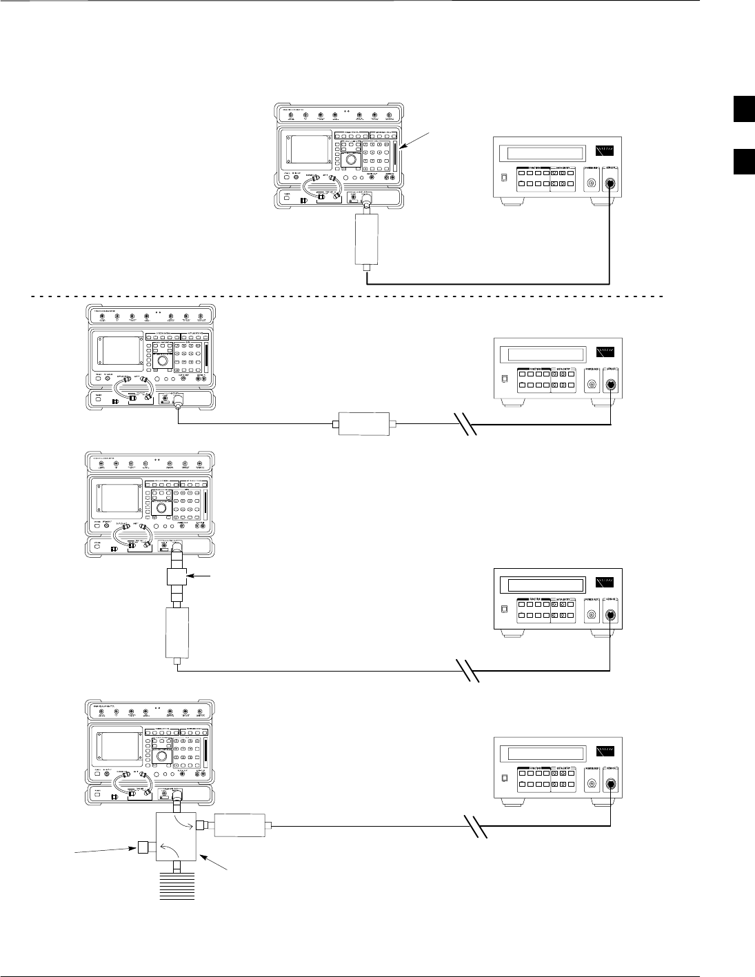
Manual Cable Calibration – continued
Jun 2004 1X SC480 BTS Hardware Installation, Optimization/ATP, and FRU B-35
DRAFT
Figure B-23: Cable Calibration Using HP8921 with PCS Interface
(A)
(C)
(A)
POWER
SENSOR
(C)
30 dB
DIRECTIONAL
COUPLER
150 W
NON–RADIATING
RF LOAD
POWER
SENSOR
(B)
POWER
SENSOR
(B)
MEMORY
CARD
SLOT
20 dB / 20 WATT
ATTENUATOR
FW00292
50 Ω
TERMINATION
POWER
SENSOR
B

Manual Cable Calibration – continued
B-36 1X SC480 BTS Hardware Installation, Optimization/ATP, and FRU Jun 2004
DRAFT
Calibrating Test Cable Setup
Using Advantest R3465
NOTE Be sure the GPIB Interface is OFF for this procedure.
Advantest R3465 Manual Test setup and calibration must be performed
at both the TX and RX frequencies.
Table B-24: Procedure for Calibrating Test Cable Setup Using Advantest R3465
Step Action
* IMPORTANT
– This procedure can only be performed after test equipment has been allowed to warm–up and
stabilize for a minimum of 60 minutes.
1Press the SHIFT and the PRESET keys located below the display
2Press the ADVANCE key in the MEASUREMENT area of the control panel.
3Select the CDMA Sig CRT menu key
4Select the Setup CRT menu key
5Using the vernier knob and the cursor keys set the following parameters
NOTE
Fields not listed remain at default
Generator Mode: SIGNAL
Link: FORWARD
Level Unit: dBm
CalCorrection: ON
Level Offset: OFF
6Select the return CRT menu key
7 Press FREQ key in the ENTRY area
8Set the frequency to the desired value using the keypad entry keys
9Verify that the Mod CRT menu key is highlighting OFF; if not, press the Mod key to toggle it OFF.
10 Verify that the Output CRT menu key is highlighting OFF; if not, press the Output key to toggle it
OFF.
11 Press the LEVEL key in the ENTRY area.
12 Set the LEVEL to 0 dBm using the key pad entry keys.
13 Zero power meter. Next connect the power sensor directly to the “RF OUT” port on the R3561L
CDMA Test Source Unit.
14 Press the Output CRT menu key to toggle Output to ON.
15 Record the power meter reading ________________________
. . . continued on next page
B

Manual Cable Calibration – continued
Jun 2004 1X SC480 BTS Hardware Installation, Optimization/ATP, and FRU B-37
DRAFT
Table B-24: Procedure for Calibrating Test Cable Setup Using Advantest R3465
Step Action
16 Disconnect the power meter sensor from the R3561L RF OUT jack.
* IMPORTANT
The Power Meter sensor’s lower limit is –30 dBm. Thus, only components having losses < 30 dB
should be measured using this method. For best accuracy, always re–zero the power meter before
connecting the power sensor to the component being calibrated. Then, after connecting the
power sensor to the component, record the calibrated loss immediately.
17 Disconnect all components in the the test setup and calibrate each one separately. Connect each
component one–at–a–time between the “RF OUT” port and the power sensor (see Figure B-24,
“Setups A, B, and C”). Record the calibrated loss value displayed on the power meter for each
connection.
Example: (A) 1st Test Cable = –0.5 dB
(B) 2nd Test Cable = –1.4 dB
(C) 20 dB Attenuator = –20.1 dB
(D) 30 dB Directional Coupler = –29.8 dB
18 Press the Output CRT menu key to toggle Output OFF.
19 Calculate the total test setup loss by adding up all the individual losses:
Example: Total test setup loss = 0.5 + 1.4 + 20.1 + 29.8 = 51.8 dB
This calculated value will be used in the next series of tests.
20 Press the FREQ key in the ENTRY area
21 Using the keypad entry keys, set the test frequency to the RX frequency
22 Repeat steps 9 through 19 for the RX frequency.
23 Refer to Chapter 3 for assistance in setting the cable loss values into the LMF.
B
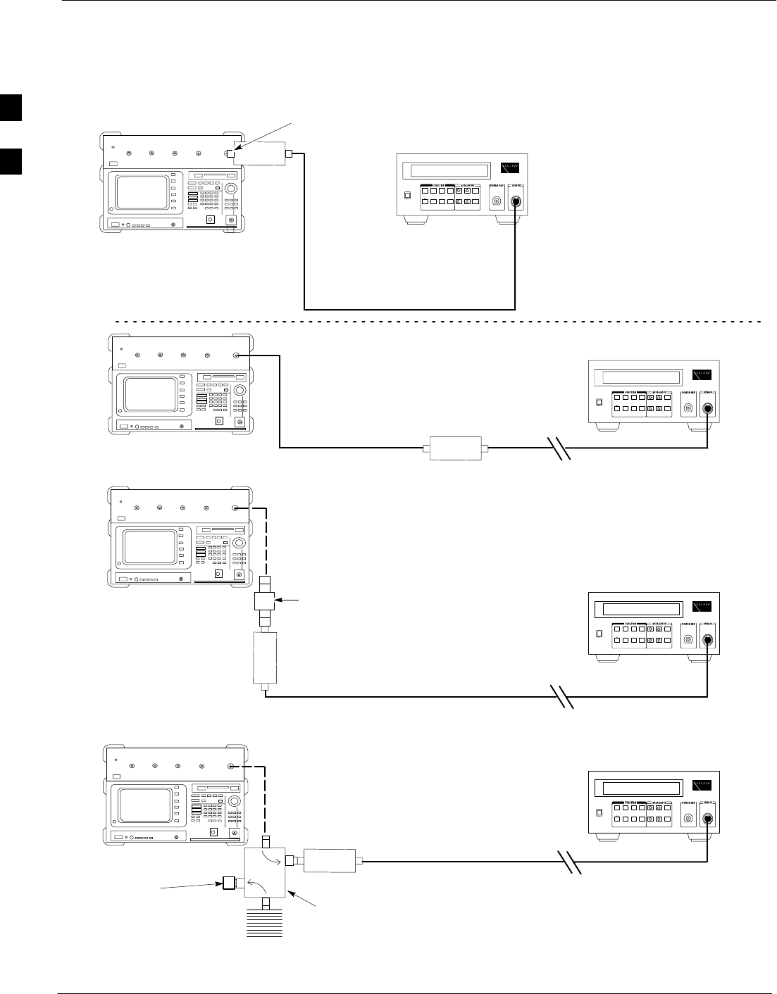
Manual Cable Calibration – continued
B-38 1X SC480 BTS Hardware Installation, Optimization/ATP, and FRU Jun 2004
DRAFT
Figure B-24: Cable Calibration Using Advantest R3465
POWER
SENSOR
20 DB / 2 WATT
ATTENUATOR
(A)
(C)
POWER
SENSOR
(D)
30 DB
DIRECTIONAL
COUPLER
(C)
100 W
NON–RADIATING
RF LOAD
POWER
SENSOR
RF OUT
POWER
SENSOR
& (B)
FW00320
50 Ω
TERMINATION
B

Jun 2004 1X SC480 BTS Hardware Installation, Optimization/ATP, and FRU
DRAFT
Appendix C: Download ROM Code
Appendix Content
Downloading ROM Code C-1 . . . . . . . . . . . . . . . . . . . . . . . . . . . . . . . . . . . . . . . . . .
Exception Procedure – Downloading ROM Code C-1 . . . . . . . . . . . . . . . . .
C

Table of Contents – continued
1X SC480 BTS Hardware Installation, Optimization/ATP, and FRU Jun 2004
DRAFT
Notes
C

Downloading ROM Code
Jun 2004 1X SC480 BTS Hardware Installation, Optimization/ATP, and FRU C-1
DRAFT
Exception Procedure –
Downloading ROM Code
This procedure is not part of a normal optimization.
Perform this procedure only on an exception basis when no alternative
exists to load a BTS device with the correct version of ROM code.
One GLI must be INS_ACT (bright green) before ROM
code can be downloaded to non–GLI devices.
NOTE
The correct ROM and RAM codes for the software release
used on the BSS must be loaded into BTS devices. To
identify the correct device ROM and RAM code loads for
the software release being used on the BSS, refer to the
Version Matrix section of the SCt CDMA Release Notes
(supplied on the tapes or CD–ROMs containing the BSS
software).
All devices in a BTS must be loaded with the ROM and
RAM code specified for the software release used on the
BSS before any optimization or ATP procedures can be
performed.
If a replacement device is loaded with ROM code which is
not compatible with the BSS software release being used,
the device ROM code can be changed using the LMF
before performing the BTS optimization and ATPs. A
device loaded with later release ROM code can not be
converted back to a previous release ROM code in the field
without Motorola assistance
CAUTION
If it is necessary to download ROM code to a device from the LMF, the
procedure in Table C-1 includes steps for both ROM and RAM code
download using the LMF.
Prerequisites
Prior to performing this procedure, ensure the correct ROM and RAM
code files exist in the LMF computer’s applicable <x>:\<lmf home
directory>\cdma\loads\<codeload#>\code folder for each of the devices
to be loaded.
C

Downloading ROM Code – continued
C-2 1X SC480 BTS Hardware Installation, Optimization/ATP, and FRU Jun 2004
DRAFT
The Release level of the ROM code to be downloaded
must be the one specified for the software release installed
in the BSS. The release level of the ROM code resident in
the other devices in the BTS must also be correct for the
BSS software release being used. ROM code must not be
downloaded to a frame loaded with code for a BSS
software release with which it is not compatible.
This procedure should only be used to upgrade
replacement devices for a BTS. It should NOT be used to
upgrade all devices in a BTS. If a BTS is to be upgraded
from R15.x to R16.0, the upgrade should be done by the
OMC–R using the DownLoad Manager.
CAUTION
Table C-1: Download ROM and RAM Code to Devices
Step Action
1Click on the device to be loaded.
NOTE
More than one device of the same type can be selected for download by either clicking on each one to
be downloaded or from the BTS menu bar Select pull–down menu, select the device item that applies.
Where: device = the type of device to be loaded (BBX, CSA, GLI, MCC)
2From the BTS menu bar Device pull–down menu, select Status.
– A status report window will appear.
3Make a note of the number in the HW Bin Type column.
NOTE
“HW Bin Type” is the Hardware Binary Type for the device. This code is used as the last four digits in
the filename of a device’s binary ROM code file. Using this part of the filename, the ROM code file
can be matched to the device in which it is to be loaded.
4 Click OK to close the status window.
5Click on the device to be loaded.
NOTE
ROM code is automatically selected for download from the <x>:\<lmf home
directory>\version folder>\<code folder> specified by the NextLoad property in
the bts–#.cdf file. To check the value of the NextLoad property, click on Util > Examine >
Display Nextload. A pop–up message will show the value of the NextLoad.
6From the BTS menu bar Device pull–down menus, select Download > ROM.
– If the file matching the Hardware Binary Type of the device is found in the code folder, a status
report shows the result of the download. Proceed to Step 11.
– If a file selection window appears, select the ROM code file manually.
7Double–click on the version folder with the desired version number for the ROM code file (for
example 2.16.0.x).
. . . continued on next page
C

Downloading ROM Code – continued
Jun 2004 1X SC480 BTS Hardware Installation, Optimization/ATP, and FRU C-3
DRAFT
Table C-1: Download ROM and RAM Code to Devices
Step Action
8Double–click the Code folder.
– A list of ROM and RAM code files will be displayed.
9! CAUTION
A ROM code file with the correct HW Bin Type must be chosen. Using a file with the wrong HW Bin
Type can result in unpredictable operation and damage to the device.
Click on the ROM code file with the filename which matches the device type and HW Bin Type
number noted in step 3 (for example, file bbx_rom.bin.0604 is the ROM code file for a BBX with a
HW Bin Type of 0604).
– The file should be highlighted.
10 Click on the Load button.
– A status report window is displayed showing the result of the download.
NOTE
If the ROM load failed for some devices, load them individually by clicking on one device, perform
steps 6 through 10 for it, and repeat the process for each remaining device.
11 Click OK to close the status window.
12 From the LMF window menu bar Tools pull–down menus, select Update NextLoad > CDMA.
13 In the left–hand pane of the window which opens, click on the BTS number for the frame being loaded
(for example, BTS–14).
14 On the list of versions displayed in the right–hand pane, click the button next to the version number of
the folder that was used for the ROM code download (for example, 2.16.0.x) and click Save.
– A pop–up message will appear showing the CDF has been updated.
15 Click on the OK button to dismiss the pop–up message.
16 Click on the device that was loaded with ROM code.
17 NOTE
RAM code is automatically selected for download.
From the BTS menu bar Device pull–down menus, select Download > Code/Data to download RAM
code and dds file data.
– A status report is displayed showing the result of the download.
18 Click OK to close the status window.
19 Observe the downloaded non–GLI device to ensure it is OOS_RAM (yellow).
20 Click on the device which was loaded with code.
21 From the BTS menu bar Device pull–down menu, select Status.
Verify that the correct ROM and RAM version numbers are displayed in the status report window.
22 Click OK to close the status window.
C

Downloading ROM Code – continued
C-4 1X SC480 BTS Hardware Installation, Optimization/ATP, and FRU Jun 2004
DRAFT
Notes
C

Jun 2004 1X SC480 BTS Hardware Installation, Optimization/ATP, and FRU
DRAFT
Appendix D: MMI Cable Fabrication
Appendix Content
MMI Cable Fabrication D-1 . . . . . . . . . . . . . . . . . . . . . . . . . . . . . . . . . . . . . . . . . . .
Purpose D-1 . . . . . . . . . . . . . . . . . . . . . . . . . . . . . . . . . . . . . . . . . . . . . . . . .
Required Parts D-1 . . . . . . . . . . . . . . . . . . . . . . . . . . . . . . . . . . . . . . . . . . . .
Cable Details D-1 . . . . . . . . . . . . . . . . . . . . . . . . . . . . . . . . . . . . . . . . . . . . .
Wire Run List D-2 . . . . . . . . . . . . . . . . . . . . . . . . . . . . . . . . . . . . . . . . . . . . . D

Table of Contents – continued
1X SC480 BTS Hardware Installation, Optimization/ATP, and FRU Jun 2004
DRAFT
Notes
D
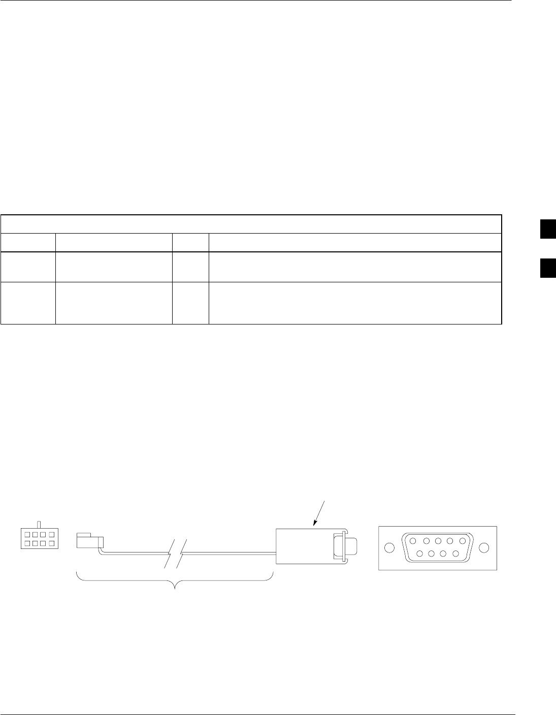
MMI Cable Fabrication
Jun 2004 1X SC480 BTS Hardware Installation, Optimization/ATP, and FRU D-1
DRAFT
Purpose
When the Motorola SLN2006A MMI Interface Kit is not available, a
cable can be fabricated by the user to interface a nine–pin serial
connector on an LMF computer platform with an MMI connector on
GLI cards and other Motorola BTS assemblies. This section provides
information necessary for fabricating this cable.
Required Parts
Table D-1: Parts Required to Fabricate MMI Cable
Item Part Number Qty Description
AMotorola 3009786R01 1Ribbon cable assembly, 1.524 M, one 8–contact MMI
connector, one 10–contact connector
BAMP 749814–1,
Belkin A4B202BGC,
or equivalent
1Receptacle kit, unassembled, 9–position, socket contacts,
unshielded, metal or plastic shell, solder or crimp–type
contacts
Cable Details
Figure D-1 illustrates the details of the fabricated MMI cable.
Figure D-1: Fabricated MMI Cable Details
DB–9 Plug
Socket Numbering
(Mating Side)
12345
6789
1
2
3
4
5
6
7
8
8–Contact MMI Plug
Socket Numbering
(Mating Side)
Item A: Cable assembly 3009786R01 (with 10–contact plug removed)
MMIFAB001–0
FABRICATION NOTES:
1. Remove 10–contact connector from ribbon cable of cable assembly 3009786R01
2. Separate wires at unterminated end of ribbon cable as required to connect to DB–9
connector contacts
3. Dark wire on ribbon cable of cable assembly 3009786R01 connects to pin 1 of the
8–contact plug
4. Strip three ribbon cable wires with connections specified in Table D-2 and connect to
DB–9 plug contacts as specified in Table D-2
5. Shorten un–connected ribbon cable wires enough to prevent contacting DB–9
contacts, leaving enough wire to egage any strain relief in the DB–9 connector shell
Item B
D

MMI Cable Fabrication – continued
D-2 1X SC480 BTS Hardware Installation, Optimization/ATP, and FRU Jun 2004
DRAFT
Wire Run List
Table D-2 provides the wire run/pin–out information for the fabricated
MMI cable.
Table D-2: Fabricated MMI Cable Wire Run List
8–CONTACT MMI
PLUG CONTACT DB–9 PLUG
CONTACT
1 ––––––––––––––––– 5
2 ––––––––––––––––– 2
3 ––––––––––––––––– 3
4No Connection (NC)
5 NC
6 NC
7 NC
8 NC
D

Jun 2004 1X SC480 BTS Hardware Installation, Optimization/ATP, and FRU
DRAFT
Appendix E: Multiple BTS Configurations
Appendix Content
Compact BTS Expansion Configuration (Indoor) E-1 . . . . . . . . . . . . . . . . . . . . . . .
Introduction E-1 . . . . . . . . . . . . . . . . . . . . . . . . . . . . . . . . . . . . . . . . . . . . . .
Materials Needed E-1 . . . . . . . . . . . . . . . . . . . . . . . . . . . . . . . . . . . . . . . . . .
External Combiner and Directional Coupler E-1 . . . . . . . . . . . . . . . . . . . . .
Frame ID Switch Settings E-2 . . . . . . . . . . . . . . . . . . . . . . . . . . . . . . . . . . .
Installation Procedure for Expansion Compact BTS with
Dual cCLPAs E-2 . . . . . . . . . . . . . . . . . . . . . . . . . . . . . . . . . . . . . . . . . . . . .
Starter and Three Expansion BTSes Interconnect Cabling for
Dual cCLPA E-3 . . . . . . . . . . . . . . . . . . . . . . . . . . . . . . . . . . . . . . . . . . . . . .
Starter and Two Expansion BTSes Interconnect Cabling for
Dual cCLPA E-5 . . . . . . . . . . . . . . . . . . . . . . . . . . . . . . . . . . . . . . . . . . . . . .
Starter and One Expansion BTSes Interconnect Cabling for
Dual cCLPA E-7 . . . . . . . . . . . . . . . . . . . . . . . . . . . . . . . . . . . . . . . . . . . . . .
Installation Procedure for Expansion Compact BTS with
Single cCLPA E-9 . . . . . . . . . . . . . . . . . . . . . . . . . . . . . . . . . . . . . . . . . . . .
Starter and Three Expansion BTSes Interconnect Cabling for
Single cCLPA E-10 . . . . . . . . . . . . . . . . . . . . . . . . . . . . . . . . . . . . . . . . . . . .
Starter and Two Expansion BTSes Interconnect Cabling for
Single cCLPA E-12 . . . . . . . . . . . . . . . . . . . . . . . . . . . . . . . . . . . . . . . . . . . .
Starter and One Expansion BTSes Interconnect Cabling for
Single cCLPA E-14 . . . . . . . . . . . . . . . . . . . . . . . . . . . . . . . . . . . . . . . . . . . .
Installation Procedure for Expansion Compact BTS
without cCLPA E-16 . . . . . . . . . . . . . . . . . . . . . . . . . . . . . . . . . . . . . . . . . . .
Starter and Expansion BTSes Interconnect Cabling
without cCLPA E-16 . . . . . . . . . . . . . . . . . . . . . . . . . . . . . . . . . . . . . . . . . . .
Starter and Two Expansion BTSes to cCLPA Cabling E-20 . . . . . . . . . . . . .
Starter and One Expansion BTS to cCLPA Cabling E-21 . . . . . . . . . . . . . . .
Multiple Compact BTS Configuration (Outdoor) E-22 . . . . . . . . . . . . . . . . . . . . . . .
Introduction E-22 . . . . . . . . . . . . . . . . . . . . . . . . . . . . . . . . . . . . . . . . . . . . . .
Materials Needed E-22 . . . . . . . . . . . . . . . . . . . . . . . . . . . . . . . . . . . . . . . . . .
External Combiner and Directional Coupler E-22 . . . . . . . . . . . . . . . . . . . . .
ExpansionCompact BTS Installation Procedure E-23 . . . . . . . . . . . . . . . . . .
Frame ID Switch Settings E-23 . . . . . . . . . . . . . . . . . . . . . . . . . . . . . . . . . . .
Other Diagrams E-26 . . . . . . . . . . . . . . . . . . . . . . . . . . . . . . . . . . . . . . . . . . .
E

Table of Contents – continued
1X SC480 BTS Hardware Installation, Optimization/ATP, and FRU Jun 2004
DRAFT
Notes
E

Compact BTS Expansion Configuration (Indoor)
Jun 2004 1X SC480 BTS Hardware Installation, Optimization/ATP, and FRU E-1
DRAFT
Introduction
This appendix covers the indoor and outdoor version of the Compact
BTS Expansion configuration. This configuration is set up for only
using other Compact BTSes. Power and ground cabling is not shown.
Figure E-1 through Figure E-3 show expansion BTSes using two
cCLPAs.
Figure E-4 through Figure E-6 show expansion BTSes using one
cCLPA.
Expansion BTSes for 1.9 GHz, +27V A or B band circuit configurations
are not supported.
Materials Needed
The following materials are required to configure expansion BTSes.
SInterconnect cabling of varying lengths
SVarious sized conduit (if used)
SData cable for cCLPA (if used)
SCustomer I/O cabling
External Combiner and
Directional Coupler
A combiner and directional coupler are required for some of the
configurations. The following are the recommended specifications for
the combiner and directional coupler.
Table E-1: Combiner and Directional Coupler Specifications
Item Specifications
Combiner
Connector: N–Type
Frequency Range: Up to 2 GHz
Insertion Loss: 3.5 dB maximum
Return Loss: 16 dB minimum
Average Input Power: 60 Watts minimum
Directional Coupler
Connector: N–Type
Frequency Range: 810 to 950 MHz
Coupling: 30 +/–1 dB
Directivity: 28 dB minimum
table continued on next page
E

Compact BTS Expansion Configuration (Indoor) – continued
E-2 1X SC480 BTS Hardware Installation, Optimization/ATP, and FRU Jun 2004
DRAFT
Table E-1: Combiner and Directional Coupler Specifications
Item Specifications
Return Loss: 18 dB minimum
Average Input Power: 10 Watts minimum
SMotorola recommended directional coupler is P/N 809643T03
SRecommended cable with combiner is Andrew LDF4–50 or
equivalent
Frame ID Switch Settings
Refer to Chapter 5, Figure 5-1 or Figure 5-2 or Table 5-1 through
Table 5-4 for the Frame DIP Switch settings.
Installation Procedure for
Expansion Compact BTS with
Dual cCLPAs
Follow the procedure in Table E-2 for installation of expansion Compact
BTS with Dual cCLPAs.
Table E-2: Procedure for Installing Expansion Compact BTS with Dual cCLPA
Step Action
1Follow the procedure in Chapter 4 for installing a Compact BTS in a rack.
2For a 3 BTS expansion configuration, follow Figure E-1. Proceed to step 3.
2a For a 2 BTS expansion configuration, follow Figure E-2. Proceed to step 3.
2b For a 1 BTS expansion configuration, follow Figure E-3. Proceed to step 3.
3If not using conduit, dress cables as necessary.
4Perform Optimization and ATP as described in Chapter 6. LMF Help provides further information.
E

Compact BTS Expansion Configuration (Indoor) – continued
Jun 2004 1X SC480 BTS Hardware Installation, Optimization/ATP, and FRU E-3
DRAFT
Starter and Three Expansion
BTSes Interconnect Cabling for
Dual cCLPA
Table E-3 shows in tabular format the interconnect cabling of
Figure E-1.
Table E-3: Starter and Three Expansion BTS Interconnect Cabling
for Circuit or Packet Configuration with Dual cCLPA
BTS Expansion 1 Expansion 2 Expansion 3 cCLPA
Starter TX–1 –––cCLPA–1 (TX IN)
Starter TX–2 –––cCLPA–2 (TX IN)
Starter EXP–TX 2 EXP TX–2 – – *cCLPA–2
Starter EXP–TX 3 –EXP TX–2 – *cCLPA–1
Starter EXP–TX 4 – – EXP TX–2 *cCLPA–2
Starter RX MAIN – – – cCLPA–1
(RX OUT)
Starter EXP–RX MAIN 2 –EXP – RX
MAIN 2 – *cCLPA–1
Starter EXP–RX MAIN 3 EXP – RX
MAIN 2 – – *cCLPA–2
Starter EXP–RX MAIN 4 – – EXP – RX
MAIN 2 *cCLPA–2
Starter RX DIV – – – cCLPA–2
(RX OUT)
Starter EXP–RX DIV 2 EXP – RX DIV
2– – *cCLPA–2
Starter EXP–RX DIV 3 –EXP – RX DIV
2– *cCLPA–1
Starter EXP–RX DIV 4 – – EXP – RX DIV
2*cCLPA–2
Starter SDCX 2 SDC INPUT
EXPANSION – – –
Starter SDCX 3 –SDC INPUT
EXPANSION – –
Starter SDCX 4 – – SDC INPUT
EXPANSION –
* Not actual physical connections to cCLPA, but software connections through the Starter BTS.
E
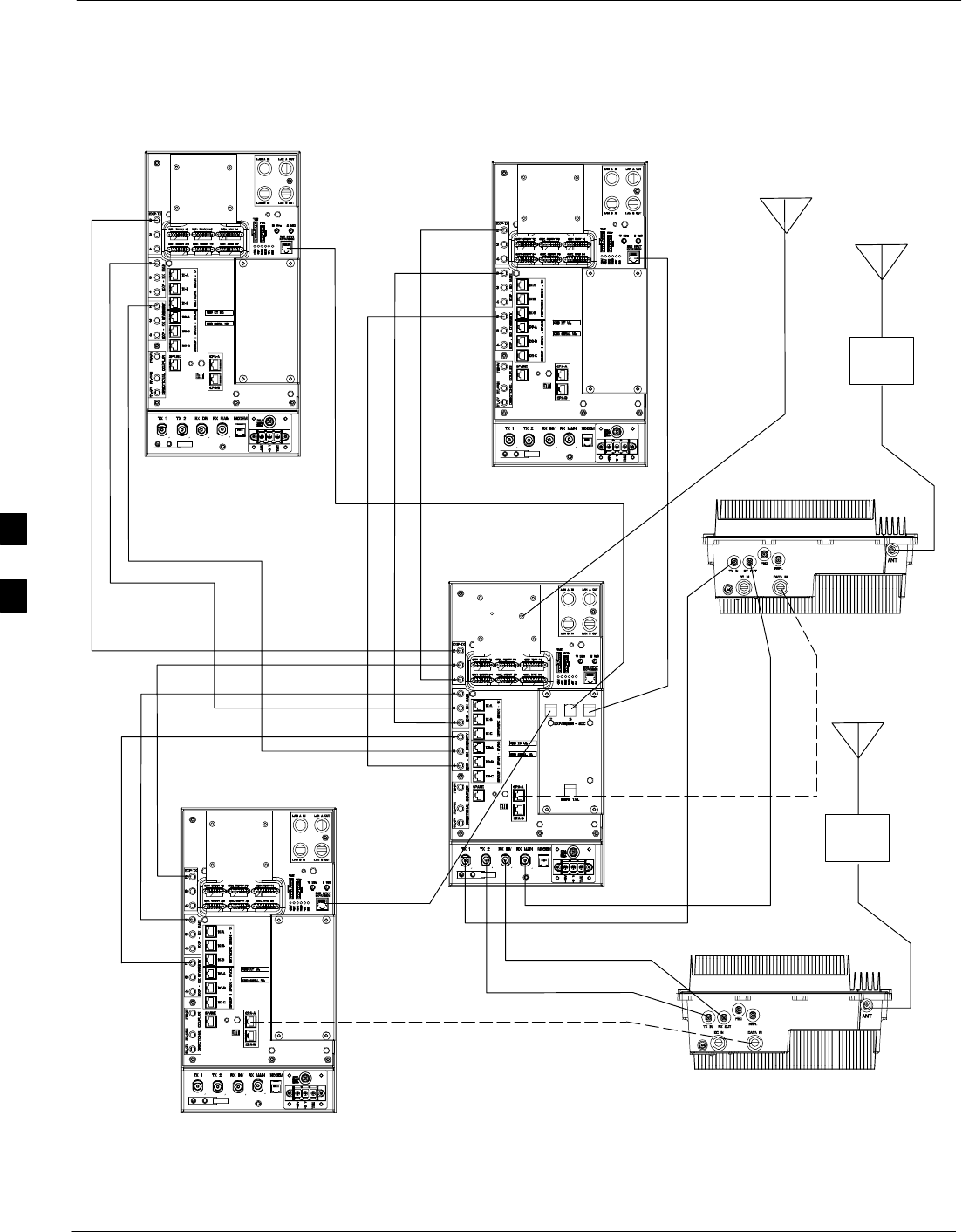
Compact BTS Expansion Configuration (Indoor) – continued
E-4 1X SC480 BTS Hardware Installation, Optimization/ATP, and FRU Jun 2004
DRAFT
Figure E-1: Three Expansion BTSes Cabling Diagram with Two cCLPAs
EXPANSION 3
EXPANSION 2
EXPANSION 1
STARTER
cCLPA 1
cCLPA 2
LOCAL GPS
Power and Ground not shown
LA
LA
Ensure that the expansion
BTSes have an Expansion
cMPC card installed.
E

Compact BTS Expansion Configuration (Indoor) – continued
Jun 2004 1X SC480 BTS Hardware Installation, Optimization/ATP, and FRU E-5
DRAFT
Starter and Two Expansion
BTSes Interconnect Cabling for
Dual cCLPA
Table E-4 shows in tabular format the interconnect cabling of
Figure E-2.
Table E-4: Starter and Two Expansion BTS Interconnect Cabling
for Circuit or Packet Configuration with Dual cCLPA
BTS Expansion 1 Expansion 2 Expansion 3 cCLPA
Starter TX–1 –––cCLPA–1 (TX IN)
Starter TX–2 –––cCLPA–2 (TX IN)
Starter EXP–TX 2 EXP TX–2 – – *cCLPA–2
Starter EXP–TX 3 –EXP TX–2 – *cCLPA–1
Starter EXP–TX 4 – – – –
Starter RX MAIN – – – cCLPA–1
(RX OUT)
Starter EXP–RX MAIN 2 EXP – RX
MAIN 2 – *cCLPA–1
Starter EXP–RX MAIN 3 EXP – RX
MAIN 2 – *cCLPA–2
Starter EXP–RX MAIN 4 – – – –
Starter RX DIV – – – cCLPA–2
(RX OUT)
Starter EXP–RX DIV 2 EXP – RX
DIV 2 – – *cCLPA–2
Starter EXP–RX DIV 3 –EXP – RX
DIV 2 – *cCLPA–1
Starter EXP–RX DIV 4 – – – –
Starter SDCX 2 SDC INPUT
EXPANSION – – –
Starter SDCX 3 –SDC INPUT
EXPANSION – –
Starter SDCX 4 – – – –
* Not actual physical connections to cCLPA, but software connections through the Starter BTS.
E
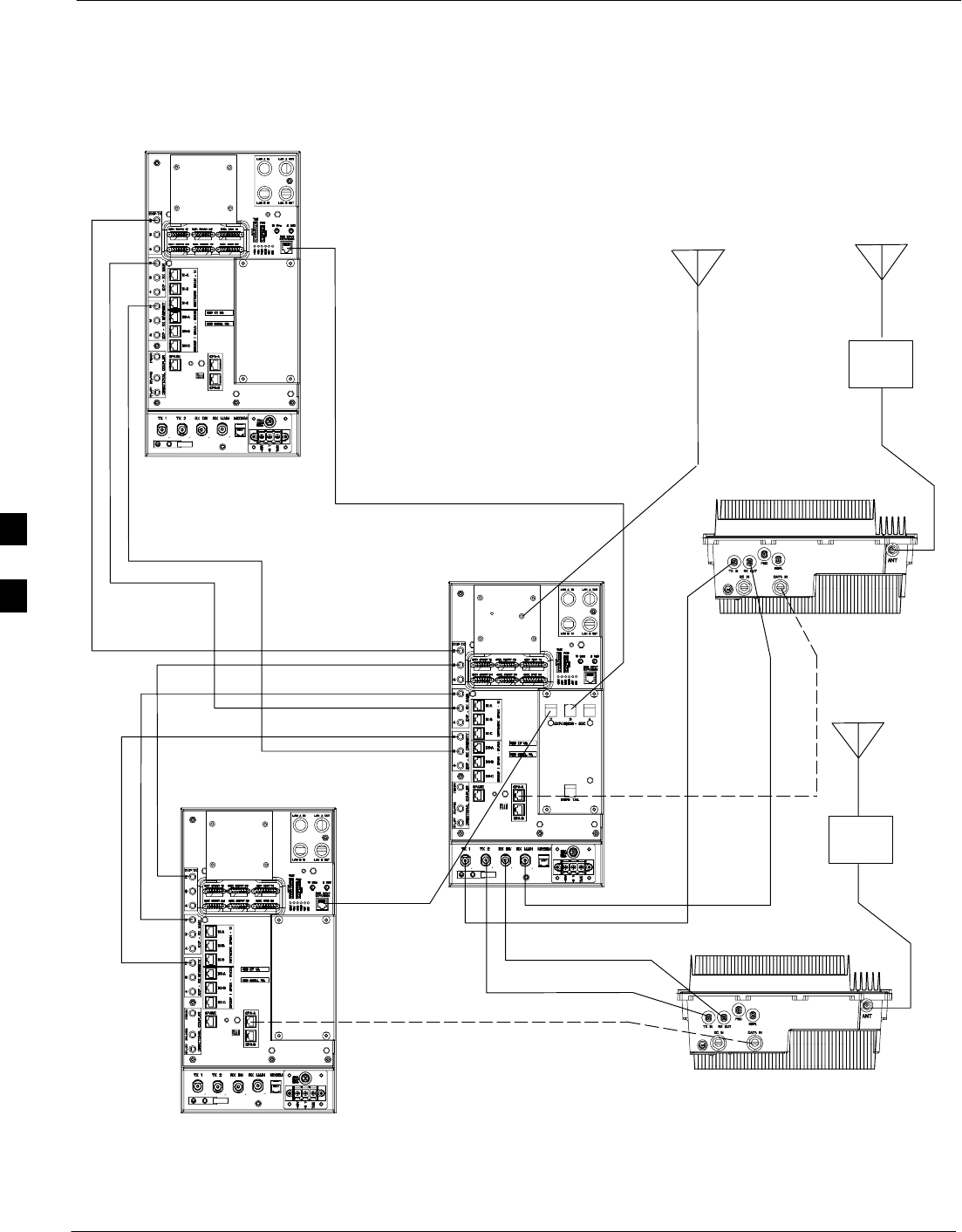
Compact BTS Expansion Configuration (Indoor) – continued
E-6 1X SC480 BTS Hardware Installation, Optimization/ATP, and FRU Jun 2004
DRAFT
Figure E-2: Two Expansion BTSes Cabling Diagram with Two cCLPAs
EXPANSION 2
EXPANSION 1
STARTER
cCLPA 1
cCLPA 2
LOCAL GPS
Power and Ground not shown
LA
LA
Ensure that the expansion
BTSes have an Expansion
cMPC card installed.
E

Compact BTS Expansion Configuration (Indoor) – continued
Jun 2004 1X SC480 BTS Hardware Installation, Optimization/ATP, and FRU E-7
DRAFT
Starter and One Expansion
BTSes Interconnect Cabling for
Dual cCLPA
Table E-5 shows in tabular format the interconnect cabling of
Figure E-3.
Table E-5: Starter and One Expansion BTS Interconnect Cabling
for Circuit or Packet Configuration with Dual cCLPA
BTS Expansion 1 Expansion 2 Expansion 3 cCLPA
Starter TX–1 –––cCLPA–1 (TX IN)
Starter TX–2 –––cCLPA–2 (TX IN)
Starter EXP–TX 2 EXP TX–2 – – –
Starter EXP–TX 3 – – – –
Starter EXP–TX 4 – – – –
Starter RX MAIN – – – cCLPA–1
(RX OUT)
Starter EXP–RX MAIN 2 – – – –
Starter EXP–RX MAIN 3 EXP – RX
MAIN 2 – – *cCLPA–2
Starter EXP–RX MAIN 4 – – – –
Starter RX DIV – – – cCLPA–2
(RX OUT)
Starter EXP–RX DIV 2 EXP – RX
DIV 2 – – *cCLPA–2
Starter EXP–RX DIV 3 – – – –
Starter EXP–RX DIV 4 – – – –
Starter SDCX 2 SDC INPUT
EXPANSION – – –
Starter SDCX 3 – – – –
Starter SDCX 4 – – – –
* Not actual physical connections to cCLPA, but software connections through the Starter BTS.
E
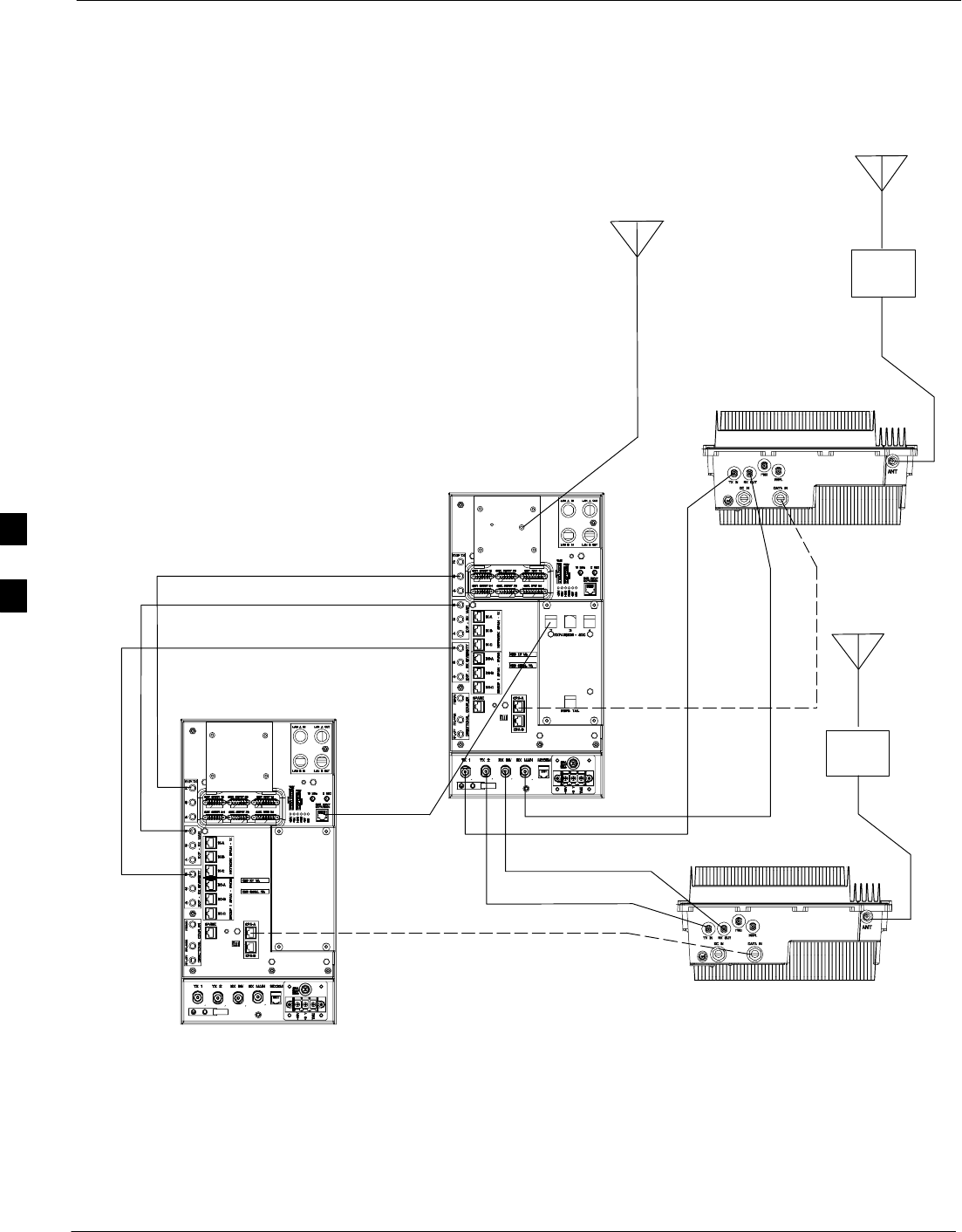
Compact BTS Expansion Configuration (Indoor) – continued
E-8 1X SC480 BTS Hardware Installation, Optimization/ATP, and FRU Jun 2004
DRAFT
LA
LA
EXPANSION 1
STARTER
cCLPA 1
cCLPA 2
LOCAL GPS
Figure E-3: One Expansion BTS Cabling Diagram with Two cCLPAs
Power and Ground not shown
Ensure that the expansion
BTS has an Expansion cMPC
card installed.
E

Compact BTS Expansion Configuration (Indoor) – continued
Jun 2004 1X SC480 BTS Hardware Installation, Optimization/ATP, and FRU E-9
DRAFT
Installation Procedure for
Expansion Compact BTS with
Single cCLPA
Follow the procedure in Table E-2 for installation of expansion Compact
BTS with Dual cCLPAs.
Table E-6: Procedure for Installing Expansion Compact BTS with Single cCLPA
Step Action
1Follow the procedure in Chapter 4 for installing a Compact BTS in a rack.
2For a 3 BTS expansion configuration, follow Figure E-4. Proceed to step 3.
2a For a 2 BTS expansion configuration, follow Figure E-5. Proceed to step 3.
2b For a 1 BTS expansion configuration, follow Figure E-6. Proceed to step 3.
3If not using conduit, dress cables as necessary.
4Perform Optimization and ATP as described in Chapter 6. LMF Help provides further information.
E

Compact BTS Expansion Configuration (Indoor) – continued
E-10 1X SC480 BTS Hardware Installation, Optimization/ATP, and FRU Jun 2004
DRAFT
Starter and Three Expansion
BTSes Interconnect Cabling for
Single cCLPA
Table E-7 shows in tabular format the interconnect cabling of
Figure E-4.
Table E-7: Starter and Three Expansion BTS Interconnect Cabling
for Circuit or Packet Configuration with Single cCLPA
BTS Expansion 1 Expansion 2 Expansion 3 cCLPA
Starter TX–1 Signals are sent thruogh an external combiner and
directional coupler
cCLPA–1 (TX IN)
Starter TX–2
directional coupler
Starter EXP–TX 2 EXP TX–2 – – *cCLPA–1
Starter EXP–TX 3 –EXP TX–2 – *cCLPA–1
Starter EXP–TX 4 – – EXP TX–2 *cCLPA–1
Starter RX MAIN – – – Antenna
Starter EXP–RX MAIN 2 EXP – RX
MAIN 2 – – *cCLPA–1
Starter EXP–RX MAIN 3 –EXP – RX
MAIN 2 – *cCLPA–1
Starter EXP–RX MAIN 4 – – EXP – RX
MAIN 2 *cCLPA–1
Starter RX DIV – – – cCLPA–1
(RX OUT)
Starter EXP–RX DIV 2 EXP – RX DIV
2– – *cCLPA–1
Starter EXP–RX DIV 3 –EXP – RX DIV
2– *cCLPA–1
Starter EXP–RX DIV 4 – – EXP – RX DIV
2*cCLPA–1
Starter SDCX 2 SDC INPUT
EXPANSION – – –
Starter SDCX 3 –SDC INPUT
EXPANSION – –
Starter SDCX 4 – – SDC INPUT
EXPANSION –
* Not actual physical connections to cCLPA, but software connections through the Starter BTS.
E
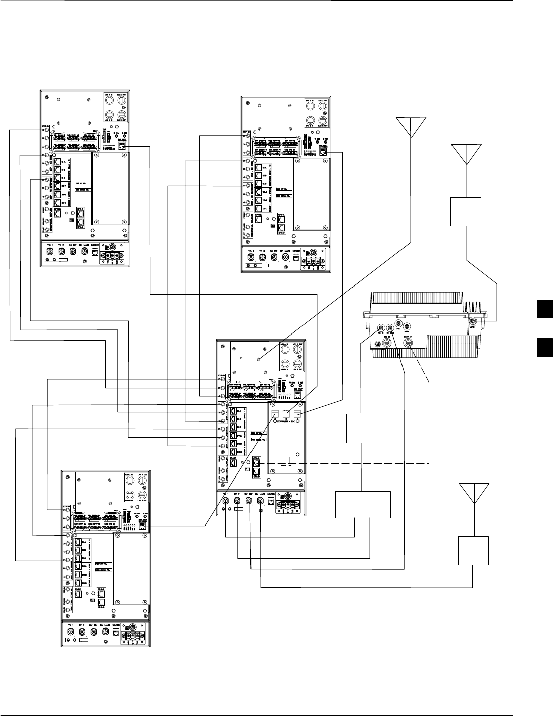
Compact BTS Expansion Configuration (Indoor) – continued
Jun 2004 1X SC480 BTS Hardware Installation, Optimization/ATP, and FRU E-11
DRAFT
Figure E-4: Three Expansion BTSes Cabling Diagram with One cCLPA
EXPANSION 3
EXPANSION 2
EXPANSION 1
STARTER
cCLPA 1
LOCAL GPS
Power and Ground not shown
COMBINER
LA
LA
RX DIV
RX MAIN
TX 1
TX 2
DC
Ensure that the expansion
BTSes have an Expansion
cMPC card installed.
E

Compact BTS Expansion Configuration (Indoor) – continued
E-12 1X SC480 BTS Hardware Installation, Optimization/ATP, and FRU Jun 2004
DRAFT
Starter and Two Expansion
BTSes Interconnect Cabling for
Single cCLPA
Table E-8 shows in tabular format the interconnect cabling of
Figure E-5.
Table E-8: Starter and Two Expansion BTS Interconnect Cabling
for Circuit or Packet Configuration with Single cCLPA
BTS Expansion 1 Expansion 2 Expansion 3 cCLPA
Starter TX–1 Signals are sent thruogh an external combiner and
directional coupler
cCLPA–1 (TX IN)
Starter TX–2
directional coupler
Starter EXP–TX 2 EXP TX–2 – – *cCLPA–1
Starter EXP–TX 3 –EXP TX–2 – *cCLPA–1
Starter EXP–TX 4 – – – –
Starter RX MAIN – – – Antenna
Starter EXP–RX MAIN 2 EXP – RX
MAIN 2 – – *cCLPA–1
Starter EXP–RX MAIN 3 –EXP – RX
MAIN 2 – *cCLPA–1
Starter EXP–RX MAIN 4 – – – –
Starter RX DIV – – – cCLPA–1
(RX OUT)
Starter EXP–RX DIV 2 EXP – RX
DIV 2 – – *cCLPA–1
Starter EXP–RX DIV 3 –EXP – RX
DIV 2 – *cCLPA–1
Starter EXP–RX DIV 4 – – – –
Starter SDCX 2 SDC INPUT
EXPANSION – – –
Starter SDCX 3 –SDC INPUT
EXPANSION – –
Starter SDCX 4 – – – –
* Not actual physical connections to cCLPA, but software connections through the Starter BTS.
E
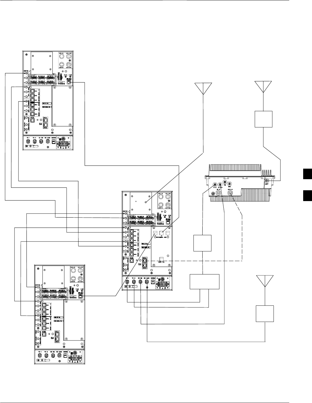
Compact BTS Expansion Configuration (Indoor) – continued
Jun 2004 1X SC480 BTS Hardware Installation, Optimization/ATP, and FRU E-13
DRAFT
Figure E-5: Two Expansion BTSes Cabling Diagram with One cCLPA
LA
EXPANSION 2
EXPANSION 1
STARTER
cCLPA 1
LOCAL GPS
Power and Ground not shown
COMBINER
LA
RX DIV
RX MAIN
TX 1
TX 2
DC
Ensure that the expansion
BTSes have an Expansion
cMPC cards installed.
E

Compact BTS Expansion Configuration (Indoor) – continued
E-14 1X SC480 BTS Hardware Installation, Optimization/ATP, and FRU Jun 2004
DRAFT
Starter and One Expansion
BTSes Interconnect Cabling for
Single cCLPA
Table E-9 shows in tabular format the interconnect cabling of
Figure E-6.
Table E-9: Starter and One Expansion BTS Interconnect Cabling
for Circuit or Packet Configuration with Single cCLPA
BTS Expansion 1 Expansion 2 Expansion 3 cCLPA
Starter TX–1 –––cCLPA–1 (TX IN)
Starter TX–2 – – – –
Starter EXP–TX 2 EXP TX–2 – – –
Starter EXP–TX 3 – – – –
Starter EXP–TX 4 – – – –
Starter RX MAIN – – – Antenna
Starter EXP–RX MAIN 2 – – – –
Starter EXP–RX MAIN 3 EXP – RX
MAIN 2 – – *cCLPA–1
Starter EXP–RX MAIN 4 – – – –
Starter RX DIV – – – cCLPA–1
(RX OUT)
Starter EXP–RX DIV 2 EXP – RX
DIV 2 – – *cCLPA–1
Starter EXP–RX DIV 3 – – – –
Starter EXP–RX DIV 4 – – – –
Starter SDCX 2 SDC INPUT
EXPANSION – – –
Starter SDCX 3 – – – –
Starter SDCX 4 – – – –
* Not actual physical connections to cCLPA, but software connections through the Starter BTS.
E
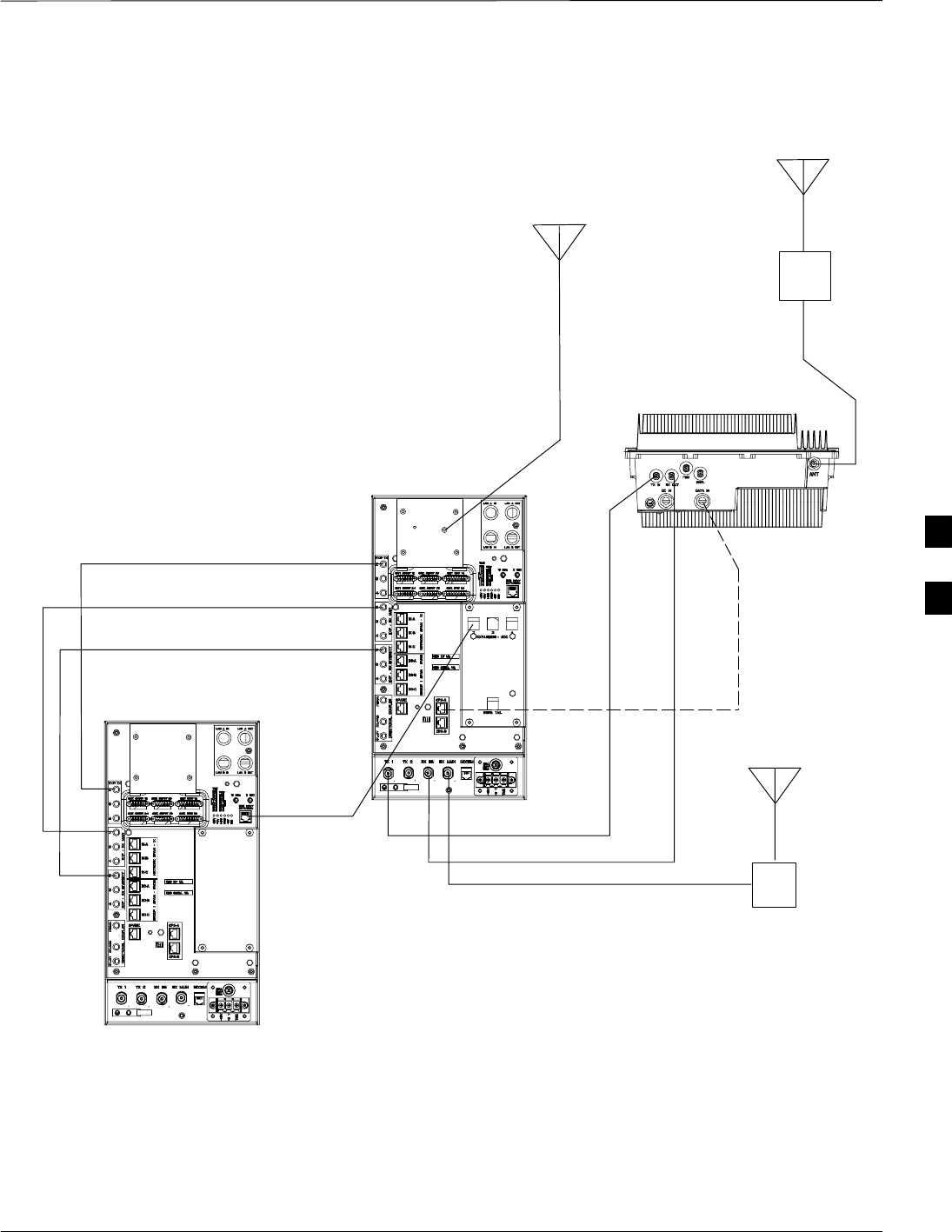
Compact BTS Expansion Configuration (Indoor) – continued
Jun 2004 1X SC480 BTS Hardware Installation, Optimization/ATP, and FRU E-15
DRAFT
LA
EXPANSION 1
STARTER
cCLPA 1
LOCAL GPS
Figure E-6: One Expansion BTS Cabling Diagram with One cCLPA
Power and Ground not shown
Ensure that the expansion
BTS has an Expansion cMPC
card installed.
LA
RX MAIN
RX DIV
TX 1
E

Compact BTS Expansion Configuration (Indoor) – continued
E-16 1X SC480 BTS Hardware Installation, Optimization/ATP, and FRU Jun 2004
DRAFT
Installation Procedure for
Expansion Compact BTS
without cCLPA
Follow the procedure in Table E-2 for installation of expansion Compact
BTS without cCLPAs. Table E-7 through Table E-9 (less the cCLPA) are
virtually the same and are can be used for the diagrams without cCLPA,
and so separate tables will not be included here.
Table E-10: Procedure for Installing Expansion Compact BTS without cCLPA
Step Action
1Follow the procedure in Chapter 4 for installing a Compact BTS in a rack.
2For a 3 BTS expansion configuration, follow Figure E-7. Proceed to step 3.
2a For a 2 BTS expansion configuration, follow Figure E-8. Proceed to step 3.
2b For a 1 BTS expansion configuration, follow Figure E-9. Proceed to step 3.
3If not using conduit, dress cables as necessary.
4Perform Optimization and ATP as described in Chapter 6. LMF Help provides further information.
Starter and Expansion BTSes
Interconnect Cabling without
cCLPA
Table E-7 through Table E-9 are virtually the same and are can be used
for the diagrams without cCLPA. Separate tables will not be included
here.
E
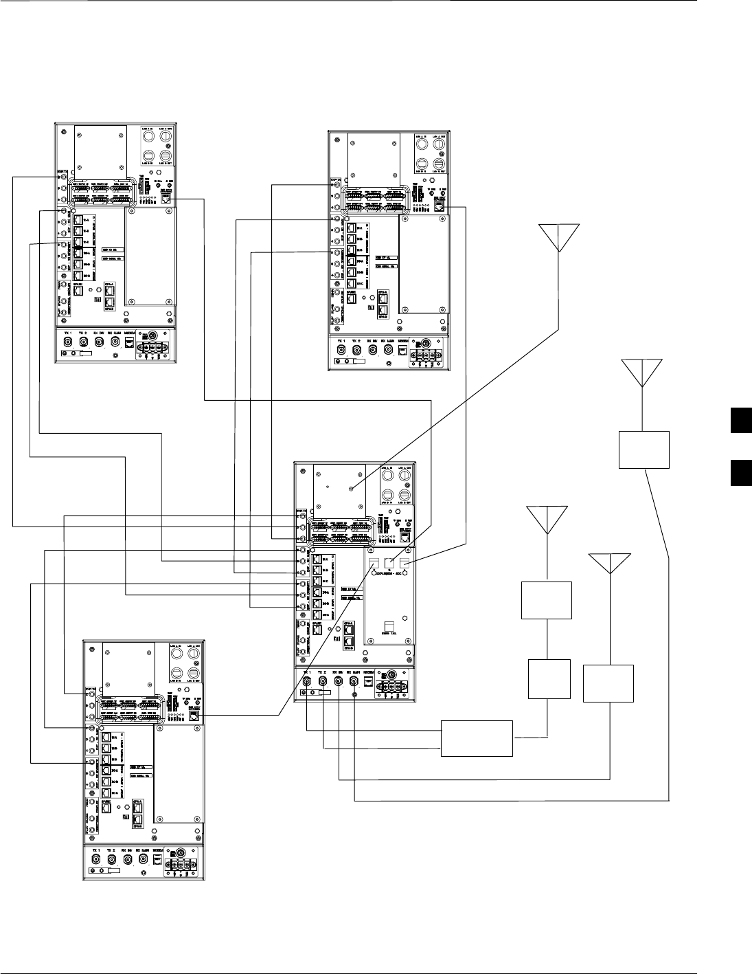
Compact BTS Expansion Configuration (Indoor) – continued
Jun 2004 1X SC480 BTS Hardware Installation, Optimization/ATP, and FRU E-17
DRAFT
Figure E-7: Three Expansion BTSes Cabling Diagram
EXPANSION 3
EXPANSION 2
EXPANSION 1
STARTER
LOCAL GPS
Power and Ground not shown
COMBINER
RX MAIN
RX DIV
TX 1
TX 2
LA
LA
LA
DC
Ensure that the expansion
BTSes have the expansion
cMPC cards installed.
E