Novatel Wireless CNN0301 1XRTT Multi-Band M2M OEM Module User Manual CNN0301IG001 HS 3001
Novatel Wireless Inc. 1XRTT Multi-Band M2M OEM Module CNN0301IG001 HS 3001
Contents
- 1. User Manual
- 2. Integration Guide
Integration Guide
CNN0301IG001
HS 3001
Integration Guide
Version: 1.04 01 July, 2013
- i -
General
TERMS OF USE OF NEW MATERIALS - PLEASE READ CAREFULLY
From time to time, Novatel Wireless, in its sole discretion, may make available for download
on its website (www.nvtl.com), or may transmit via mail or email, updates or upgrades to, or
new releases of, the firmware, software or documentation for its products (collectively, 'New
Materials'). Use of such New Materials is subject to the terms and conditions set forth below,
and may be subject to additional terms and conditions as set forth in Novatel Wireless's
Technical Support Policy (posted on its website) and/or any written agreement between the
user and Novatel Wireless.
All New Materials are provided AS IS. Novatel Wireless makes no warranty or representation
with respect to the merchantability, suitability, functionality, accuracy or completeness of any
such New Materials. The user of such New Materials assumes all risk (known or unknown) of
such use. Novatel Wireless reserves all rights in such New Materials. The user shall have only a
revocable and limited license to use such New Materials in connection with the products for
which they are intended. Distribution or modification of any New Materials without Novatel
Wireless's consent is strictly prohibited.
IN NO EVENT WILL NOVATELWIRELESS BE RESPONSIBLE FOR ANY INCIDENTAL,
INDIRECT, CONSEQUENTIAL OR SPECIAL DAMAGES AS A RESULT OF THE USE OF ANY
NEW MATERIALS. NOVATELWIRELESS 'S MAXIMUM LIABILITY FOR ANY CLAIM BASED
ON THE NEW MATERIALS SHALL NOT EXCEED FIFTY U.S. DOLLARS ($50).
Version Verification
Please ensure you have the latest version of this document by downloading it from
www.nvtl.com
- ii -
Copyright
© 2013 Novatel Wireless. All rights reserved. Complying with all applicable copyright laws is
the responsibility of the user. Without limiting the rights under copyright, no part of this
document may be reproduced, stored in or introduced into a retrieval system, or transmitted
in any form or by any means (electronic, mechanical, photocopying, recording or otherwise),
or for any purpose, without the express written permission of Novatel Wireless.
Novatel Wireless and the Novatel Wirelesslogo are either registered trademarks or
trademarks of Novatel Wireless M2M, Inc. in the United States.
251 Renner Pkwy
Richardson, TX 75080 USA
Phone: (972) 633-4400
Fax: (972) 633-4444
Email: info@nvtl.com
www.nvtl.com
- iii -
Warranty Information
[Revised: 11/11/2010]
This warranty applies to (a) products sold directly by Novatel Wireless M2M, unless a different
warranty is specified in a written agreement between Novatel Wireless M2M and the
purchaser; and (b) products sold to end users through a distributor authorized by Novatel
Wireless M2M, but only where the authorized distributor does not provide a separate
warranty on such products, and Novatel Wireless M2M has agreed to provide this warranty to
such end users. If you purchased the product from an authorized distributor, please check
whether this warranty from Novatel Wireless M2M, or a separate warranty from the
distributor, applies to your purchase. This warranty does not apply to any (i) accessories or
batteries for the products; or (ii) demonstration samples or prototypes of the products. Unless
otherwise provided in a written agreement between Novatel Wireless M2M and the
purchaser, all such accessories, batteries, samples or prototypes are provided by Novatel
Wireless M2M AS IS without any warranty of any kind.
Novatel Wireless M2M warrants to the original purchaser of the product from Novatel
Wireless M2M or its authorized distributor (as applicable) that, for a period of one (1) year
from the date of shipment of the product from Novatel Wireless M2M, the product hardware
will be substantially free from defects in material or workmanship under normal operation, and
the product firmware will perform substantially in accordance with the product
documentation provided by Novatel Wireless M2M. Novatel Wireless M2M does not warrant
that (a) the product hardware or firmware will meet the purchaser's requirements; (b) the
operation of the product hardware or firmware will be uninterrupted or error-free; or (c) the
product, when integrated in, or combined with, other products or software not supplied by
Novatel Wireless M2M, will continue to perform substantially in accordance with the product
documentation. This limited warranty is for the benefit of the original purchaser, and is not
transferable.
During the warranty period, Novatel Wireless M2M, at its expense and in its sole discretion,
will repair the product, or replace the product with a corresponding or equivalent product, if
it is determined to have a covered defect, provided that the purchaser first notifies Novatel
Wireless M2M (directly or through its authorized distributor from which the product was
purchased) of any such defect, furnishes Novatel Wireless M2M with a proof of purchase (if
required), requests and obtains a return merchandize authorization (RMA) number from
Novatel Wireless M2M, and returns the product under that RMA to Novatel Wireless M2M (or,
at Novatel Wireless M2M's option, to its authorized distributor), with the shipping charges
being prepaid by purchaser. If, upon reasonable examination of the returned product, Novatel
Wireless M2M does not substantiate the defect claimed by purchaser, or determines that the
defect is not covered under this limited warranty, Novatel Wireless M2M will not be required
to repair or replace the product, but may instead reship the product to the purchaser (or, at
Novatel Wireless M2M's option, to its authorized distributor where the product can be made
- iv -
available to purchaser), in which case the purchaser shall be responsible for paying Novatel
Wireless M2M's cost for reshipping the product to purchaser (or to Novatel Wireless M2M's
authorized distributor), and Novatel Wireless M2M's usual charges for unpacking, testing, and
repacking the product for reshipment to purchaser (or to Novatel Wireless M2M's authorized
distributor).Purchaser shall bear the risk of loss or damage in transit to any product returned
by purchaser to Novatel Wireless M2M, or any returned product not found to be defective or
covered under this warranty, and reshipped by Novatel Wireless M2M to purchaser (or to
Novatel Wireless M2M's authorized distributor). In the event Novatel Wireless M2M repairs or
replaces a defective product covered by this limited warranty, the repaired or replacement
product will be covered under this limited warranty for the remainder of the original warranty
period on the defective product, or a period of ninety (90) days, whichever is longer. If
Novatel Wireless M2M is unable to repair or replace a defective product covered by this
limited warranty, Novatel Wireless M2M will provide to purchaser a credit or a refund (at
Novatel Wireless M2M's option) of the original purchase price (excluding taxes and shipping
charges). Any returned and replaced product, or any product for which Novatel Wireless M2M
has furnished a credit or a refund, becomes the property of Novatel Wireless M2M.
Novatel Wireless M2M shall not have any obligation to provide any firmware bug fixes,
upgrades or new releases except as may be necessary to correct any covered defect of which
purchaser notifies Novatel Wireless M2M in writing during the warranty period. Novatel
Wireless M2M, from time to time and in its sole discretion, may make available for download
on its website (www.nvtl.com), or may provide via email, certain firmware bug fixes,
upgrades or new releases for the product. Download and use of any such bug fixes, upgrades
or new releases is subject to all of the applicable terms and conditions of Novatel Wireless
M2M's technical support policy as posted and updated on its website.
Novatel Wireless M2M shall have no obligation under this limited warranty for (a) normal wear
and tear; (b) the cost of procurement of substitute products; or (c) any defect that is (i)
discovered by purchaser during the warranty period but for which purchaser does not
request an RMA number from Novatel Wireless M2M, as required above, until after the end of
the warranty period, (ii) caused by any accident, misuse, abuse, improper installation,
handling or testing, or unauthorized repair or modification of the product, (iii) caused by use
of any materials not supplied by Novatel Wireless M2M, or by use of the product other than in
accordance with its documentation, or (iv) the result of electrostatic discharge, electrical
surge, fire, flood or similar causes.
The purchaser (or its customers, as applicable) shall be solely responsible for the proper
configuration, testing and verification of the Novatel Wireless M2M product prior to
deployment in the field, and for ensuring that any end user product or system into which the
Novatel Wireless M2M product is integrated or incorporated operates as intended and meets
the requirements of purchaser (or its customers). Novatel Wireless M2M shall have no
responsibility whatsoever for the integration, configuration, testing, verification, installation,
upgrade, support or maintenance of any such end user product or system, or for any liabilities,
damages, costs or expenses associated therewith.
- v -
Novatel Wireless M2M'S SOLE RESPONSIBILITY AND PURCHASER'S SOLE REMEDY UNDER
THIS LIMITED WARRANTY SHALL BE FOR Novatel Wireless M2M TO REPAIR OR REPLACE
THE PRODUCT (OR IF REPAIR OR REPLACEMENT IS NOT POSSIBLE, PROVIDE A CREDIT
OR REFUND OF THE PURCHASE PRICE) AS PROVIDED ABOVE. Novatel Wireless M2M
EXPRESSLY DISCLAIMS ALL OTHER WARRANTIES OF ANY KIND, EXPRESS OR IMPLIED,
INCLUDING WITHOUT LIMITATION ANY IMPLIED WARRANTIES OF NON-INFRINGEMENT,
MERCHANTABILITY, SATISFACTORY PERFORMANCE AND FITNESS FOR A PARTICULAR
PURPOSE. IN NO EVENT SHALL Novatel Wireless M2M BE LIABLE FOR ANY INDIRECT,
SPECIAL, EXEMPLARY, INCIDENTAL OR CONSEQUENTIAL DAMAGES (INCLUDING
WITHOUT LIMITATION LOSS OR INTERRUPTION OF USE, DATA, REVENUES OR PROFITS)
RESULTING FROM A BREACH OF THIS WARRANTY OR BASED ON ANY OTHER LEGAL
THEORY, EVEN IF Novatel Wireless M2M HAS BEEN ADVISED OF THE POSSIBILITY OR
LIKELIHOOD OF SUCH DAMAGES.
Some jurisdictions may require a longer warranty period than specified above and,
accordingly, for products sold in those jurisdictions the applicable warranty period shall be
extended as required under the laws of those jurisdictions. Furthermore, some jurisdictions
may not allow the disclaimer of implied warranties or the exclusion or limitation of incidental
or consequential damages, so the above disclaimer, limitation or exclusion may not apply to
products sold in those jurisdictions. This limited warranty gives the purchaser specific legal
rights and the purchaser may have other legal rights that vary from jurisdiction to jurisdiction.
This limited warranty shall be governed by the laws of the State of Texas, United States of
America, without regard to conflict of laws principles. This limited warranty shall not be
governed in any respect by the United Nations Convention on Contracts for the International
Sale of Goods.

- vi -
Regulatory Compliance
FCC CERTIFICATION
Novatel Wireless M2M certifies that the Enabler HS 3001 CDMA Radio Module (FCC ID:
MIVCNN0301) complies with the RF requirements applicable to broadband PCS equipment
operating under the authority of 47 CFR Part 24, Subpart E and Part 22 Subpart H of the FCC
Rules and Regulations. This certification is contingent upon installation, operation and use of
the Enabler HS 3001 module and its host product in accordance with all instructions provided
to both the OEM and end user. When installed and operated in a manner consistent with the
instructions provided, the Enabler HS 3001 module meets the maximum permissible exposure
(MPE) limits for general population / uncontrolled exposure as defined in Section 1.1310 of the
FCC Rules and Regulations.
The Enabler HS 3001 module is designed for use in a variety of host units, "enabling" the host
platform to perform wireless data communications. However, there are certain criteria relative
to integrating the modem into a host platform such as a PC, laptop, handheld, monitor and
control unit, etc. that must be considered to ensure continued compliance with FCC
compliance requirements.
Important Information for Canada/USA OEM Integrators
This section provides guidance for using the Enabler HS 3001 in host devices through the FCC
Permissive Change process. When utilizing the permissive change process, Novatel Wireless,
the grantee, is responsible for all integrations and must be consulted on all regulatory matters
involving the Enabler HS 3001.
The Enabler HS 3001 module is granted with FCC/IC modular approval for mobile 1
applications, and may be installed as a standalone2transmitter in final products meeting the
following conditions. If the following conditions are followed, it may be used in final products
without additional FCC/IC certification. Otherwise, additional FCC/IC approvals must be
obtained.
1Mobile Device Definition – FCC defines as a transmitting antenna located at a distance ≥
20cm from the user.
2Standalone is defined as a single transmitter transmitting as opposed to 2 or more
transmitters transmitting simultaneously.

- vii -
lThe antenna connected to the Enabler HS 3001 module must be installed to provide at
least 20 cm separation from the human body at all times.
lThe Enabler HS 3001 module and transmitter antennas must not be co-located with any
other transmitter or antenna within a host device.
lThe transmitter antenna used with the Enabler HS 3001 module must not exceed the
following levels:
lBand Class 0: the maximum gain is 2.2 dBi.
lBand Class 1: the maximum gain is 8 dBi.
lTo comply with the aspects of KDB996369, strict adherence to the design parameters in
Section 4.1.1.3 Antenna And RF Signal Trace must be observed. Section 4.1.1.3 provides
PCB RF trace design guidelines for the coplanar microstrip between the Enabler HS
3001 RF compression pads and the U.FL style coaxial connector.
lA label containing the FCC and Industry Canada IDs must be permanently affixed to the
exterior of the host device into which the Enabler HS 3001 module is installed. The label
may also be under a panel or battery pack if it is readily accessible and cannot be
separated from the host device itself. The label must contain a statement similar to the
following;
lThis device contains FCC ID: MIVCNN0301
lThis equipment contains equipment certified under IC: 4160A-CNN0301
If any of these conditions are not met then additional information should be sought from the
FCC or an FCC qualified test laboratory.
If the Enabler HS 3001 module is intended for use in a portable1device, the OEM integrator is
responsible to design the product to comply with RF exposure, and must work with Novatel
Wireless (the grantee) to satisfy FCC/IC SAR requirements. Refer to FCC OET Bulletin 65
Supplement C for information about FCC RF exposure compliance requirements for mobile
and portable devices.
The system user manuals and other documentation must clearly indicate operating conditions
that must be observed to ensure compliance with FCC/IC RF exposure guidelines and also
include appropriate caution and warning statements and information.
The host device containing the Enabler HS 3001 module may also require compliance to FCC
Part 15 Subpart B – Unintentional Radiators.
1Portable Device Definition – FCC defines as a transmitting antenna located at a distance ≤
20cm from the user.
- viii -
FCC NOTICE TO USERS
Novatel Wireless M2M has not approved any changes or modifications to this device by the
user. Any changes or modifications could void the users authority to operate the device. See
47 CFR Sec. 15.21. The device complies with part 15 of the FCC rules. Operation is subject to
the following two conditions: (1) This device may not cause harmful interference, and (2) this
device must accept any interference received, including interference that may cause
undesired operation. See 47 CFR Sec. 15.19.
This equipment has been tested and found to comply with the limits for a Class B digital
device, pursuant to part 15 of the FCC rules. These limits are designed to provide reasonable
protection against harmful interference in a residential installation. This equipment generates,
uses, and can radiate radio frequency energy and, if not installed and used in accordance with
the instructions, may cause harmful interference to radio communications. However, there is
no guarantee that interference will not occur in a particular installation. If this equipment does
cause harmful interference to radio or television reception, which can be determined by
turning the equipment off and on the user is encouraged to try to correct the interference by
one or more of the following measures:
lReorient or relocate the receiving antenna.
lIncrease the separation between the equipment and receiver.
lConnect the equipment into an outlet on a circuit different from that to which the
receiver is connected.
lConsult the dealer or an experienced radio/TV technician for help.
If the FCCID of the module is not visible when installed in the host platform, then a
permanently attached or marked label must be displayed on the host unit referring to the
module.
The label should contain wording such as:
Contains FCC ID: MIVCNN0301
This device complies with Part 15 of the FCC Rules. Operation is subject to the following two
conditions: (1) This device may not cause harmful interference, and (2) This device must
accept any interference received, including interference that may cause undesired operation.
Industry Canada
IC: 4160a-CNN0301 MODEL NUMBER: CNN0301
This device complies with Industry Canada licence-exempt RSS standard(s). Operation is
subject to the following two conditions: (1) this device may not cause interference, and (2) this
device must accept any interference, including interference that may cause undesired
operation of the device.
- ix -
In order to use the Enabler HS 3001 module without any additional FCC certification the
installation must meet the following conditions:
lThe system antenna(s) connected to the Enabler HS 3001 module must be installed to
provide at least 20 cm separation from the human body during normal operation.
lThe system antennas must not be co-located with any other transmitter or antenna.
lThe system antenna(s) used with the Enabler HS 3001 module must not exceed the
following levels:
lBand Class 0: the maximum gain is 0 dBi.
lBand Class 1: the maximum gain is 8 dBi.
Le présent appareil est conforme aux CNR d'Industrie Canada applicables aux appareils radio
exempts de licence. L'exploitation est autorisée aux deux conditions suivantes: (1) l'appareil
ne doit pas produire de brouillage, et (2) l'utilisateur de l'appareil doit accepter tout
brouillage radioélectrique subi, même si le brouillage est susceptible d'en compromettre le
fonctionnement.
Afin d'utiliser le Enabler HS 3001 module sans aucune certification de d'Industrie Canada
supplémentaire l'installation doit satisfaire aux conditions suivantes:
lL'utilisation du système connectée au module de Enabler HS 3001 doit être installée
pour fournir la séparation d'au moins 20 cm du corps humain pendant une opération
normale.
lLes antennes du système ne doivent pas être colocalisés avec un autre émetteur ou
antenne.
lL'utilisation du système utilisée avec le module de Enabler HS 3001 ne doit pas dépasser
les niveaux suivants:
lGroupe classe 0: le gain maximal est 0 dBi.
lGroupe classe 1: le gain maximal est 8 dBi.
ROHS COMPLIANCE
As a part of Novatel Wireless M2M’s corporate policy of environmental protection, Novatel
Wireless M2M takes every step to ensure that the HS 3001 modules are designed and
manufactured to comply to the European Union Directive 2002/95/EC for the Restriction of
Hazardous Substances (RoHS).
NCC NOTICE
「減少電磁波影響,請妥適使用」
NCC ID: CCAF133G0170T1
- x -
Important Safety Information
The following information applies to the devices described in this manual. Always observe all
standard and accepted safety precautions and guidelines when handling any electrical device.
lSave this manual: it contains important safety information and operating instructions.
lDo not expose the HS 3001 product to open flames.
lEnsure that liquids do not spill onto the devices.
lDo not attempt to disassemble the product: Doing so will void the warranty. This
product does not contain consumer-serviceable components.
The Enabler HS 3001 module may not be used in an environment where radio frequency
equipment is prohibited or restricted in its use. This includes aircrafts, airports, hospitals, and
other sensitive electronic areas.
Do not operate RF devices in an environment that may be susceptible to radio interference
resulting in danger, specifically;
lAreas where prohibited by the law.
lFollow any special rules and regulations and obey all signs and notices. Always
turn off the host device when instructed to do so, or when you suspect that it may
cause interference or danger.
lWhere explosive atmospheres may be present.
lDo not operate your modem in any area where a potentially explosive atmosphere
may exist. Sparks in such areas could cause an explosion or fire resulting in bodily
injury or even death. Be aware of and comply with all signs and instructions.
lUsers are advised not to operate the modem while they are at a refueling point or
service station.
lUsers are reminded to observe restrictions on the use of radio equipment in fuel
depots (fuel storage and distribution areas), chemical plants or where blasting
operations are in progress.
lAreas with a potentially explosive atmosphere are often but not always clearly marked.
lPotential locations can include gas stations, below deck on boats, chemical transfer
or storage facilities, vehicles using liquefied petroleum gas (such as propane or
butane), areas where the air contains chemicals or particles, such as grain, dust or
metal powders, and any other area where you would normally be advised to turn
off your vehicle engine.
lNear Medical and life support equipment.
lDo not operate your modem in any area where medical equipment, or life support
equipment may be located, or near any equipment that may be susceptible to any
form of radio interference. In such areas, the host communications device must be
turned off. The modem may transmit signals that could interfere with this
equipment.
lOn an aircraft, either on the ground or airborne.
lIn addition to FAA requirements, many airline regulations state that you must
suspend wireless operations before boarding an airplane. Please ensure that the
host device is turned off prior to boarding an aircraft in order to comply with these
regulations. The modem can transmit signals that could interfere with various
onboard systems and controls.
- xi -
lWhile operating a vehicle
lThe driver or operator of any vehicle should not operate a wireless data device.
Doing so will detract from the driver or operator's control and operation of that
vehicle. In some countries, operating such communication devices while in control
of a vehicle is an offense.
Disclaimer
The information and instructions contained within this publication comply with all FCC, GCF,
PTCRB, R&TTE, IMEI and other applicable codes that are in effect at the time of publication.
Novatel Wireless M2M disclaims all responsibility for any act or omissions, or for breach of law,
code or regulation, including local or state codes, performed by a third party.
Novatel Wireless M2M strongly recommends that all installations, hookups, transmissions, etc.,
be performed by persons who are experienced in the fields of radio frequency technologies.
Novatel Wireless M2M acknowledges that the installation, setup and transmission guidelines
contained within this publication are guidelines, and that each installation may have variables
outside of the guidelines contained herein. Said variables must be taken into consideration
when installing or using the product, and Novatel Wireless M2M shall not be responsible for
installations or transmissions that fall outside of the parameters set forth in this publication.
Novatel Wireless M2M shall not be liable for consequential or incidental damages, injury to
any person or property, anticipated or lost profits, loss of time, or other losses incurred by
Customer or any third party in connection with the installation of the Products or Customer's
failure to comply with the information and instructions contained herein.

- xii -
Table of Contents
1 Introduction 1
Technical Specifications 3
Reference Documents 5
Typical Usage 5
Contacting Novatel Wireless M2M 5
2 Module Power 6
Operating Power 7
Typical Input Current 7
3 Interfaces 8
Module Mounting To Host Board (Reference) 9
Mounting Tab Soldering Guidelines 12
Connectors 13
RF Board-to-Board Connector Option 13
I/O Connector Pin Assignments 13
Specific Absorption Rate (SAR) Guidelines 16
SAR Compliance 17
4 Hardware Design Guidelines 18
Advanced Tips For An RF-Friendly Layout 19
Ground Plane 19
Thermal Relief 20
Modem Mounting Tabs 22
Antenna And RF Signal Trace 23
Engineering Layer Stack-up And Impedance 25
VBAT Input 25
Audio Reference Design 26

- xiii -
Audio Schematics 27
Control Connector Signal Descriptions And Functions 29
Module Power (PINS 87, 89, 91, 93, 95, 97, 99) 29
Modem Power-on And Recovery Techniques 30
Power Switch Logic Detect (Pin 85) 30
ON/OFF (PIN 37) 30
Phone On - PON (PIN 35) 31
Internal Power Switch 32
Voltage Reference - VREG_MSME1.8 (PIN 77) 33
USB (PINS 1, 3, 5, 7) 33
General Purpose Input/Output Interface 33
RTC Sleep 34
Serial Interfaces And Handshake (Pins 11, 13, 15, 17, 19, 21, 23, 25) 35
UART 2 (Pins 27, 29) 36
Digital Audio Interface (Pins 12, 14, 16, 18) 36
Digital Audio Configuration 36
Digital Audio Data Format 36
32 KHz Output (PIN 56) 37
Analog-to-Digital Inputs (PIN 44 And 74) 37
Handset Microphone Input (PINS 65, 67) 38
Handset Microphone BIASOutput (PINS 53, 63) 38
Handset Speaker Output (PINS 71, 73) 38
Headset Microphone Input (PIN 55) 38
Headset Speaker Output Left And Right (PINS 57, 59) 39
Headset Detect (PIN 47) 39
Circuit Protection 39
5 USB Driver Installation 41
USB Driver Installation (Windows XP) 42


- 2 -
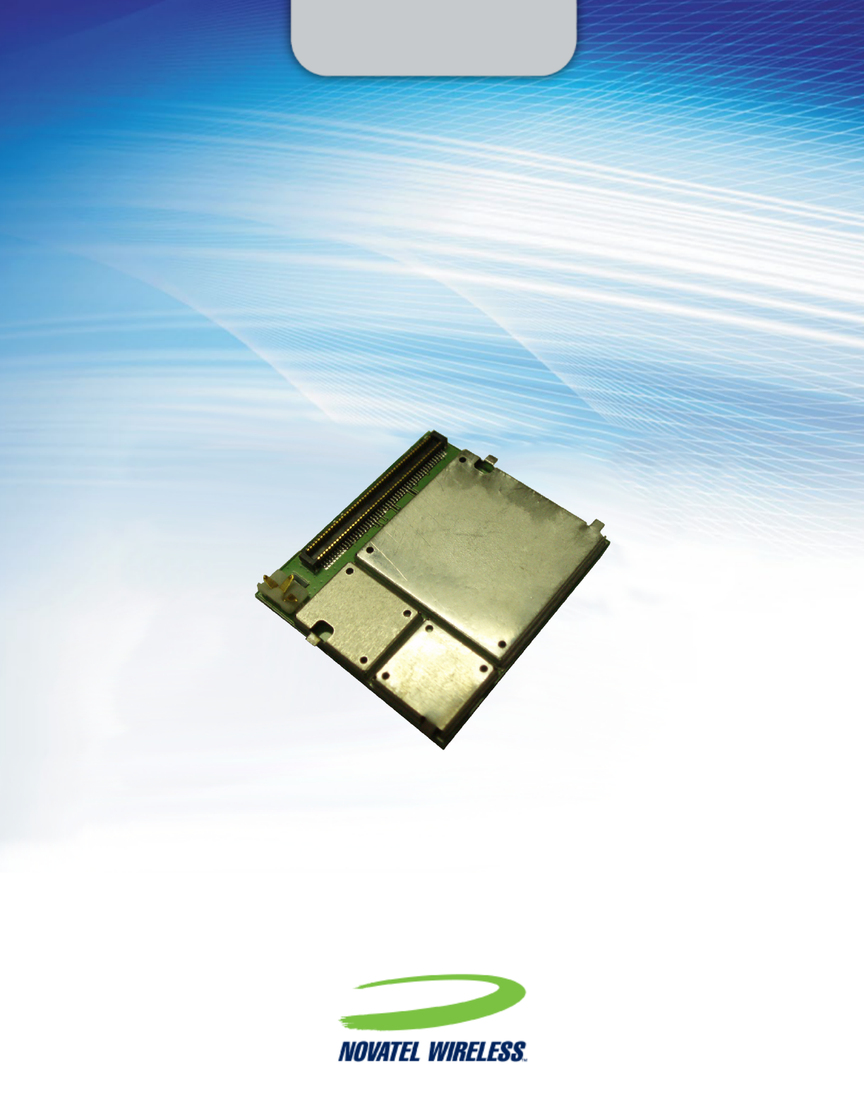
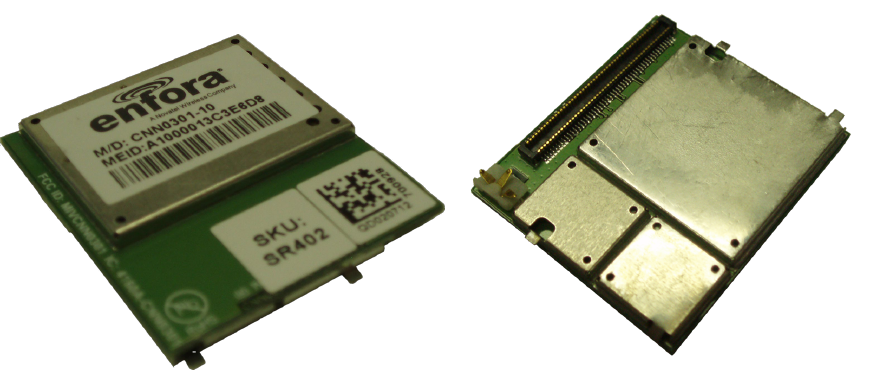
The HS 3001 modem is a compact, wireless OEM module that uses the Code Division Multiple
Access (CDMA) international communications standard to provide two-way wireless
capabilities. The HS 3001 module is a fully approved CDMA device, enabling application-
specific, two-way communication and control.
The small size of the HS 3001 module allows it to integrate easily into the application and
packaging.
Figure 1-1 HS 3001 Module
- 3 -
Technical Specifications
Housing
lSize (L x W x H): 28.0 mm x 25.0 mm x 4.50
mm
lWeight: 4.13 grams
Interfaces
lHost Interface: Serial Interface
lData input/output
interface:
100 position 0.4 mm pitch con-
nector (Molex P/N 55909-
1074)
lPrimary serial port: V.24 protocol, 1.8V levels,
UART implementation, Hard-
ware flow control
lUSB port: USB serial port and USB Debug
(USB Debug is Novatel Wire-
less M2M Use only)
lGPIO: Up to 8 GPIO
lAudio: Analog and Digital audio
lVoice: Supports Handset and Headset
audio interfaces
lAntenna Interface: B2B Spring contact
lCommand protocol: Novatel Wireless M2M Packet
API, CDMA AT Command set
lReference clock: 32 kHz output reference clock
(accessible via 100-pin con-
nector)
lADC: 2 ADC inputs
lUART2: 2.85 V
lLogic: lUART1
lPCM
lDigital Audio
lGPIO
lPWON
lPower Control
Outputs
lHandset earphone outputs (EARP, EARN pins)
lHeadset 32 Ωstereo outputs (HSOL, HSOR pins)
Mechanical: Storage And
Transportation
lTransportation
vibration,
packaged:
ASTM D999
lDrop,
packaged:
ASTM D775 method A, 10 drops
Application Interface
lUSB: 3.4V
lVBUS: 5.0V
lMic Bias Out: 1.8V @ 1.5 mA max.
lAudio Mic Inputs: 1.0 Vp-p ±12%
lEar Audio Out: 1.11 – 1.40 VRMS into 32 Ω(1.25
VRMS typical)
lHeadset Out L&R: 0.531 to 0.668 VRMS into 16 Ω
(0.595 VRMS Typical)
Power
lElectrical Power: 3.4 to 4.4 Vdc (vbat)
Supply Vripple must be less
than 25 mV across all fre-
quencies
lPeak currents and
average power
dissipation:
Refer to the Operating Power
table in the Technical Spe-
cifications for peak currents
and average power dissipation
for various modes of operation.
Radio Features
lCDMA Sensitivity
(Typical):
≤-108 dBm
lFrequency bands: BC0-800 MHz –US Cell, BC1-
1900 MHz – US PCS
lRadio Mode: CDMA 1xRTT, 153 kbps FL/RL
lChipset: Qualcomm QSC1110
Audio Features
lHeadset Microphone biasing
lHandset Microphone biasing
lHeadset Plug/Unplug detection
lHandset microphone input (MICIN, MICIP pins)
lHeadset microphone input (HSMIC pin)
Environmental
lCompliant
Operating
Temperature
-20 °C to 60 °C (CDMA Spec
Compliant)
lOperating
Temperature
-30 °C to 70 °C
lStorage
Temperature
-40 °C to 85 °C
lHumidity Up to 95% non condensing
lEmissions FCC 47 CFR Parts 2,15,22 & 24
- 4 -
Mechanical: Operational
lOperational
vibration
Random IEC60068-2-64 / MIL-
STD-202G Method 214A
50-2000 Hz, 7.56 GRMS, 3 Axis,
8 Hours per axis
Packet Data Transfer
lProtocol CDMA 1xRTT (153 kbps UL and
DL)
lShort Message
Services
Text, MO/MT
Regulatory
lAgency approvals FCC Certification
Industry Canada

- 5 -
Reference Documents
lCNN0301AT001 - HS 3001 AT Command Reference
lCNN0301TG001 - HS 3001 Transition Guide
lENF0000SD001 - HDK Guide
lCNN0301AN001- Using Digital Audio on the HS 3001
Typical Usage
The following applications can use the HS 3001 module for transmitting/receiving data/voice:
lAutomated Meter Reading (AMR)
lPoint of Sale Applications (POS)
lE-mail and Internet access
lAutomated Vehicle Location (AVL)
lMachine to Machine communication (M2M)
lTelematics
lTelemetry
lWireless Security
lSmart Phones
lTelemedicine
Contacting Novatel Wireless M2M
For technical support and customer service dealing with the modem itself, contact the
company where you purchased the product. If you purchased the product directly from
Novatel Wireless M2M, visit the Support page on the Novatel Wireless M2M web site:
www.nvtl.com


- 7 -
Operating Power
The HS3001 module requires an in/out voltage of 3.4V to 4.4V. The supply ripple must be less
than 25mV across all frequencies.
Typical Input Current
Typical Results @ 3.6 V, 20 deg C, with 1000 μF at connector input on VBAT and RF
terminated into a 50 Ωresistive load. Traffic Data Rate: Full
Band Mode Avg
(mA)
Peak
(mA) Notes
BC0 RC3, 3.6 V Max Power 23.5 dBm 540 590 RC3= Radio Config 3
BC0 RC3, 3.6 V, TX=0 dBm 180 180
BC1 RC3, 3.6 V Max Power 23.5 dBm 600 680
BC1 RC3, 3.6 V, TX=0 dBm 230 230
Both Idle-Slot Cycle Index=2, Sleep=3 <2.0 80 Modem registered; peak during network activity
Both Sleep (not registered) 0.9
Both Shutdown 0.03 0.08 For minimum current draw in shut down mode, we
recommend you shut down the modem by either
sending AT$OFF (AT$OFFDLY must be >0) or by send-
ing a pulse on PON line (pin 35), and then setting the
ON/OFF line (pin 37) low to remove power from the
device.

- 9 -
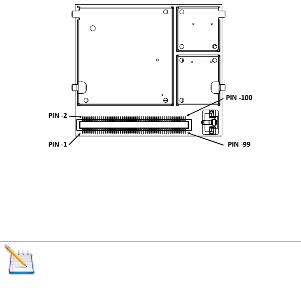
Figure 3-1 Pin 1 Reference, 100-Pin I/O Connector
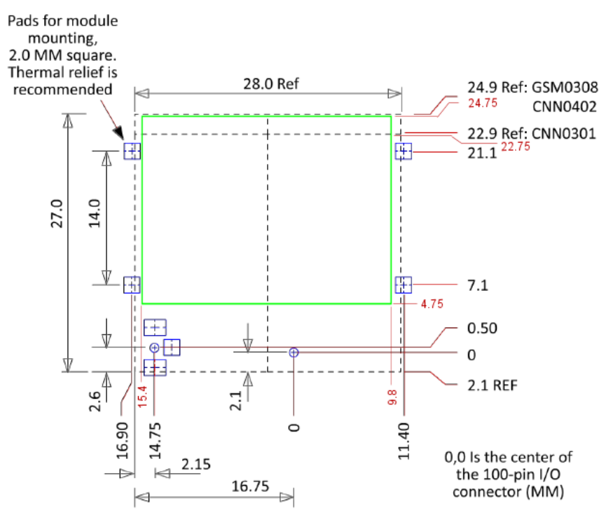
Module Mounting To Host Board (Reference)
Solder the module to a PCB using the mounting tabs provided.
These tabs provide circuit grounding for the module.
Do not add solder paste to mounting pads, RF connector, or shield pads.
The only portion recommended for thermal relief is along the outer edge of each
pad, where you would place a soldering iron. The rest of the pad should be solid
flood to the copper ground underneath the module. (See Figure 5) This is critical
for helping heat dissipation.
- 10 -
Figure 3-2 Host Board Layout
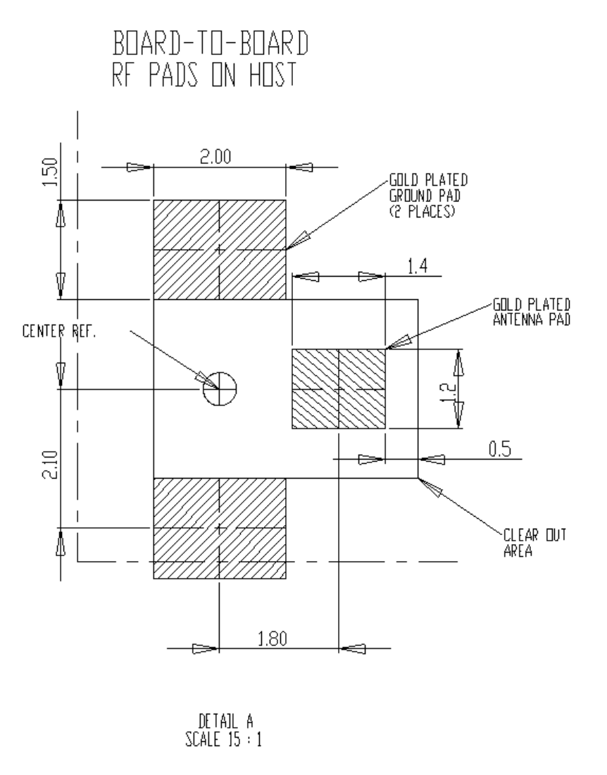
- 11 -
Figure 3-3 Host Pads for Board-To-Board RF Connector
- 12 -
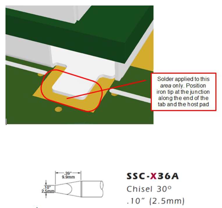
Mounting Tab Soldering Guidelines
Do not apply excessive solder during module mounting. Solder bridging to internal
components can occur if you use an overly large iron tip and hold it against the vertical shield
walls while applying solder at the junction between the iron and the module. Coverage of the
outer ¾ of the tab is sufficient for securing the module. Please see the diagram below:
Figure 3-4 Module Tab Soldering
The iron tip should not exceed the size of that shown below for the Metcal SSC-x36A series
tip.
Figure 3-5 Recommended Tip Size

- 13 -
Connectors
On the Modem: 100-Pin I/O Connector, Plug, SMT, Dual Row, 0.4 mm Pitch
lNovatel Wireless M2M PN = CON-1040-0100
lMolex PN = 55909-1074
On the Host: 100-Pin I/O Connector, Socket, SMT, Dual Row, 0.4 mm Pitch (Mate to module)
lNovatel Wireless M2M PN = CON-1040-0101
lMolex PN = 51338-1074
The mated height of the two connectors is 1.50 mm.
RF Board-to-Board Connector Option
On The Modem:
Novatel Wireless M2M PN = CON-0009-0006
Sunridge PN = MCE-15A-G01
No connector required on the host PCB.
I/O Connector Pin Assignments
The following table shows the pin assignments for the input/output connector.
Pin Function Description Notes
01 VBUS USB Power
02 GND Ground
03 VBUS USB Power
04 GND Ground
05 USB_DP USB Data (+)
06 Reserved N/A was LED sink on GSM0308
07 USB_DM USB Data (-)
08 Reserved N/A was current sink for LED A on
GSM0308
09 Reserved N/A was ID_USB on GSM0308
10 Reserved N/A was VRWLED on GSM0308
11 UART_RTS UART RTS
12 PCM_DIN Digital Audio I/F Data In
13 UART_CTS UART CTS

- 14 -
Pin Function Description Notes
14 PCM_CLK Digital Audio Clock
15 UART_RX UART1 RX (Output)
16 PCM_SYNC Digital Audio Interface Sync
17 UART_DTR Data Terminal Ready
18 PCM_DOUT Digital Audio I/F Data Out
19 UART_DCD Data Carrier Detect
20 Reserved N/A was GPIO 18 on GSM0308
21 UART_TX UART1 TX (input) was SPI_MOSI on GSM0308
22 Reserved N/A was GPIO 15 on GSM0308
23 UART_RING UART_RING
24 Reserved N/A was GPIO 16 on GSM0308
25 UART_DSR Data Set Ready
26 Reserved N/A was GPIO 14 on GSM0308
27 UART2_TX UART 2 TX was reserved on GSM0308
28 Reserved N/A was GPIO 17 on GSM0308
29 UART2_RX UART 2 RX
30 Reserved N/A was GPIO 13 on GSM0308
31 Reserved N/A
32 Reserved N/A was GPIO 20 on GSM0308
33 Reserved N/A
34 Reserved N/A was GPIO 9 on GSM0308
35 PON "Phone on" - Use the momentary
low function to activate.
See section 4.2 for details.
was PWR_CTL on GSM0308
36 Reserved N/A
37 ON/OFF Power Control Switch Input
High = Modem ON
Low/Float = Modem OFF
See section 4.2 for details.
was RESET on GSM0308
38 Reserved N/A
39 Reserved N/A
40 Reserved N/A
41 Reserved N/A
42 Reserved N/A

- 15 -
Pin Function Description Notes
43 Reserved N/A
44 ADC2 Analog In #2 was reserved on GSM0308
45 Reserved N/A
46 Reserved N/A
47 HSDETECT Headset Detect
48 Reserved N/A
49 Reserved N/A
50 Reserved N/A
51 Reserved N/A
52 Reserved N/A
53 HSMICBIAS Headset Microphone Bias Connected internally to pin 63
54 GND Ground
55 HSMIC Microphone (+)
56 CLK32K_BUF Buffered 32.678 kHz clock output
(not XTAL)
57 HSOL Headset Out Left (+)
58 GPIO 4 General Purpose IO
59 HSOR Headset Out Right (+)
60 GPIO 3 General Purpose IO
61 Reserved N/A was HSOVMID on GSM0308
62 GPIO 2 General Purpose IO
63 MICBIAS Microphone Bias Connected internally to pin 53
64 GPIO 1 General Purpose IO
65 MICIP Microphone differential input (+)
66 GPIO 7 General Purpose IO
67 MICIN Microphone differential input (-)
68 GPIO 5 General Purpose IO
69 GND Ground
70 GPIO 6 General Purpose IO
71 EARP Handset speaker (+)
72 GPIO 8 General Purpose IO
73 EARN Handset speaker (-)
74 ADCIN Analog In #1

- 16 -
Pin Function Description Notes
75 GND Ground
76 Reserved N/A was SIM VDD on GSM0308
77 VRIO Reference Voltage (< 5 mA) for
external interfaces
78 Reserved N/A was SIM CLK on GSM0308
79 Reserved N/A
80 Reserved N/A was SIM RST on GSM0308
81 Reserved N/A
82 Reserved N/A was SIM IO on GSM0308
83 Reserved N/A was VBACKUP on GSM0308
84 Reserved N/A was SIM Detect on GSM0308
85 PSLOGIC Power Switch Logic Select was VBAT on GSM0308
86 GND Ground/Power Return/Shield
87 VBAT Power Input
88 GND Ground
89 VBAT Power Input
90 GND Ground
91 VBAT Power Input
92 GND Ground
93 VBAT Power Input
94 GND Ground
95 VBAT Power Input
96 GND Ground
97 VBAT Power Input
98 GND Ground
99 VBAT Power Input
100 GND Ground
Table 3-1 I/O Connector Pin Assignments
Specific Absorption Rate (SAR) Guidelines
Portable RF exposure evaluation must be completed on host devices that provide ≤20.0 cm
of separation distance between the transmitter antenna and the end user.
- 17 -
Portable Device Definition
FCC defines as a transmitting antenna located at a distance ≤20cm from the user.
Mobile Device Definition
FCC defines as a transmitting antenna located at a distance ≥20cm from the user.
SAR Compliance
European and US certification bodies require that you test Specific Absorption Rate (SAR).
SAR is a measure of energy absorbed by organic tissue over a specific time. The factors that
affect SAR readings are:
loutput power
lfrequency of the radiation
lproximity to antenna
lantenna counterpoise
lduty cycle
Early in the physical design stage of the UE, the antenna and the mechanical engineering
design teams must collaborate on the design to ensure that they can meet the SAR
requirements. Carefully reading and understanding the FCC requirements can help designers
choose the antenna type, the antenna location, and the industrial design of the UE. The
placement and characteristics of the main antenna are the most critical factors affecting SAR
performance.


- 19 -
Use the following guidelines to successfully implement your PCB layout to obtain the best
performance, the lowest possible EMI emissions, the maximum thermal conduction, the
highest mechanical integrity, and the best voice quality. The HS 3001 module is a compact,
high performance design, yet it is easy to interface into the final product. To experience its full
potential, designers should pay close attention to ground structures, the routing of RF and
Digital traces, and the size of the power supply lines.
These design tips are strictly guidelines and are not meant to be a complete list
of items that guarantee actual performance. Each application is different and may
require variation from these guidelines; however, you should try to use these
sound engineering principles.
Advanced Tips For An RF-Friendly Layout
Use the following tips for an RF-friendly layout:
Ground Plane
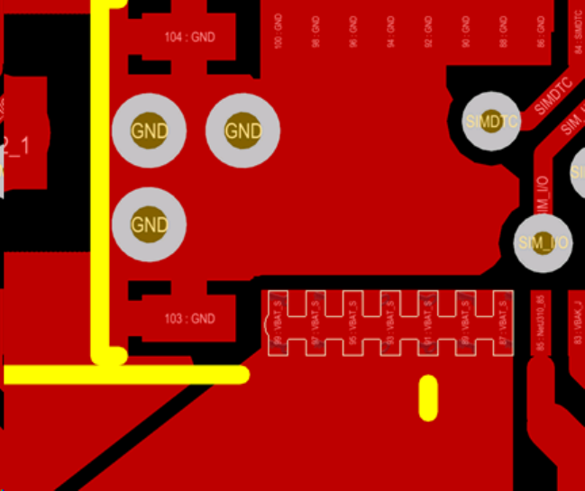
To ensure the lowest possible EMI emissions and maximum thermal conductivity, Novatel
Wireless M2M recommends that you solder all metal tabs on the cellular module shield down
onto a continuous ground plane that runs under the entire module. Provide ample ground vias
around the metal tabs to create a low impedance ground. Minimize the number of I/O and
power traces and vias under the cellular module to allow for as much ground plane as
possible. Great care should also be taken to avoid any shorting or coupling of vias that might
be placed under the radio module and have them masked.
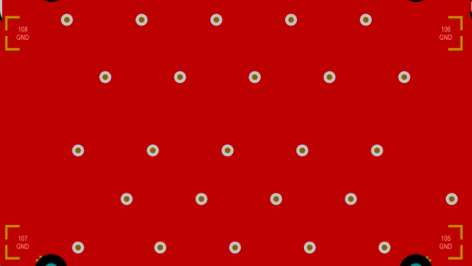
An example of a good ground structure and pad layout follows:
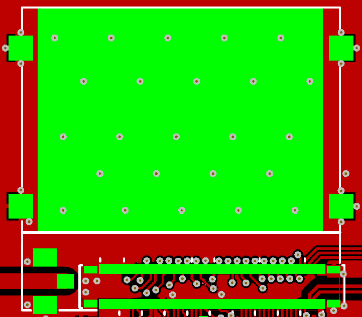
- 20 -
Figure 4-1 Example of good ground plane for CDMA modules
Thermal Relief
Because the ground plane acts as a large heat sink, it can affect the solderability of
components. A common method to reduce this effect is to use thermal relief around the pad
in question. However, you must be careful when using thermal relief for high current or high
frequency applications.
For example, a large thermal relief can serve the purpose for general applications such as low
current, low speed data lines, DC connections, and audio-frequency applications. However,
you should avoid such thermal relief structures for applications involving high current and/or
high-frequency (such as those using the cellular module). Depending on the frequency of
operation, the long narrow thermal relief traces between the pad and the ground plane act
like an RF choke. These RF chokes become higher impedance at harmonics of the
fundamental frequency making it problematic for high-frequency suppression. This can make
it difficult to pass type approval testing.
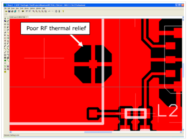
- 21 -
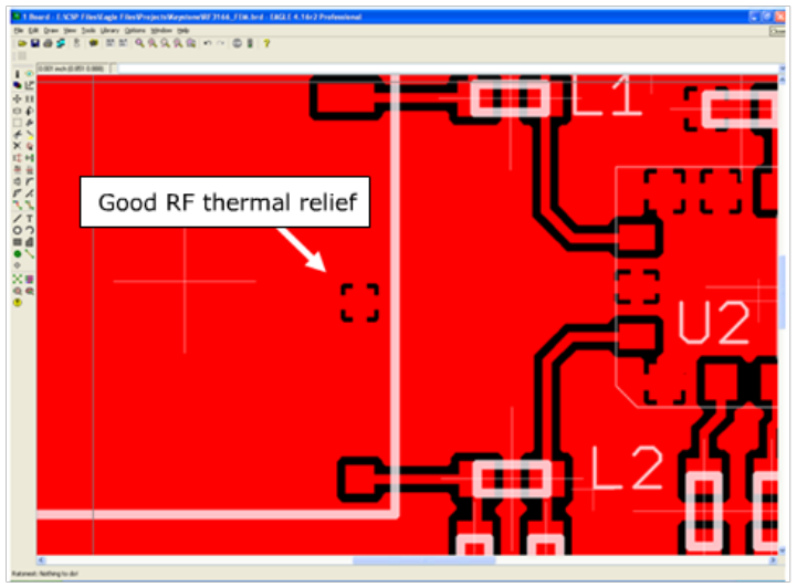
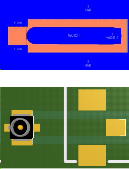
Figure 4-2 Example of a POOR RF Thermal Relief
If thermal relief is necessary, use short, fat traces. This will still provide a solderable
connection, while providing a better RF connection. Making the traces shorter also allows for a
more continuous ground plane due to less copper being removed from the area. We also
recommend that you have ground vias around all thermal relief of critical ground pins such as
the five cellular shield tabs.
- 22 -
Figure 4-3 Example of a GOOD RF Thermal Relief
Modem Mounting Tabs
Soldering the tabs on the module is an important part of the assembly of the module and host
board. The following figure shows an ideal ground structure for the tabs. One half of the pad is
covered with a solid ground. This allows for a low impedance connection while still providing
some thermal relief for the soldering process. While soldering the tabs, apply slight pressure
(approximately 500 grams of force) to the module to flex the tabs and place the module as
close to the host as possible.
- 23 -
Figure 4-4 Modem Tabs - Ideal Ground Structure
Antenna And RF Signal Trace
The PCB trace that feeds the RF output port must be designed for a 50 ohm characteristic
impedance. The RF trace should be coplanar, or routed into internal layers to keep the top
layer continuous around and underneath the cellular module. Provide ample ground vias
around the RF contacts, the RF trace, and launch pad. If possible, keep I/O and power traces
away from the RF port. This includes traces running parallel or orthogonal to it. Do not use
thermal relief on the antenna output port ground pads. Pay close attention to the size of the
pad and thickness of the dielectric beneath the signal pad and trace. Most PCB manufacturers
can adjust the trace width to maintain 50 ohms impedance if the traces are identified and
instructions are included on the FAB drawing. This service is typically provided at no or
minimal additional cost.
For minimum RF emissions due to the fundamental frequency of operation, the cellular
module works best with an antenna load that has a VSWR of 1.5:1 or better. The antenna
should not have gain at the harmonic frequencies, otherwise, the conducted harmonics could
get amplified to a point where the product no longer passes type approval. However, for
applications where antenna quality is less than ideal, we recommend that you have a low pass
filter (Pi structure with N=3) in the RF path to the antenna. This is a secondary plan should
there be a need to lower harmonic levels at frequencies above the PCS band. The pad
structure may also be used to match the antenna load impedance, if required. If it is not
needed, you may use a low-reactance capacitor to bridge the Pi structure.
- 24 -
The RF cable going between the cellular module and the antenna is very lossy; therefore, you
should keep the length of this cable as short a possible.
The following design parameters are for the coplanar microstrip between the Module RF
compression pads and the U.FL style coaxial connector.
The coplanar waveguide microstrip details are shown below.
- 25 -
Engineering Layer Stack-up And Impedance
Layer Line Width/Space (mil) Control Impedance (Ω)
L1 51.18/24 mil 50 ± 10%
L1 1 oz +plating
CORE 0.3 11.81mil
L2 1 oz
PP 3313 3.3003mil
CORE 0.6 23.62mil
PP 3313 3.3198mil
L3 1 oz
CORE 0.3 11.81mil
L4 1 oz +plating
Overlap THK: 1.47 mm Material : FR4 IT-180A
Finish THK: 1.6 ± 0.16 mm
Layer LW/LS(mil) Calculate Value (Ω) H1(mil)Er1 H2(mil)Er2
L1 55/22.09 mil ± 5% 50.6 (coplanar waveguide) 43.3 ± 5% 4.24
L3 Ground
VBAT Input
The HS 3001 VBAT input can have a relative high current draw that can fluctuate rapidly,
especially when transmitting at max power and burst mode. The VBAT interface must be
designed to provide the required instantaneous voltage and current with minimal voltage
droop. This includes both sufficient bulk decoupling capacitance as well as adequate layout
provisions.
When laying out the connections to the cellular module interface connector, it is tempting to
use traces of the same width as the connector pins. However, this is a very compact connector
and traces of that width will not have sufficient copper. Similar to the discussion on thermal
relief, the use of narrow traces to connect the VBAT pins to the source voltage can act like a
high impedance and cause a significant voltage droop when higher currents are required.
If the VBAT drops too low, the cellular modules will reset. To minimize the trace loss, use a
larger trace that spans several pins. Any concern about solderability can be mitigated by
using a solder mask with cutouts for the individual pins as shown in the figure below. The
layout should provide sufficient trace width over the entire trace from the Enable modules all
the way to the source of the VBAT voltage. Any transitions between layers for this trace should
use multiple vias.
- 26 -
Even the best layout will have some impedance from the source to the cellular module;
therefore, sufficient bulk decoupling capacitance is required at the Vbat input to the cellular
module. If necessary, you may use up to two 1000 µF, low ESR, tantalum capacitors to provide
the desired decoupling. If used, the capacitors should be located very close to the cellular
interface connector VBAT pins. Any thermal relief used on these capacitors should comply with
the information given above to provide the lowest possible impedance. The grounding of
these capacitors is critical. Therefore, it should be a low impedance and should use multiple
vias to the internal ground plane close to the capacitor.
It is highly recommended to have the battery voltage be set at 3.8 Volts (the approximate
midpoint between 3.4 Volt and 4 .4 Volt) to avoid any negative side effects related to
transmit power of the radio module caused by high voltage drops due to high current draw
on the Vbat line.
Figure 4-5 Example of GOOD VBAT layout
Audio Reference Design
The audio quality is dependent on the circuit design and layout. As an aid to obtaining good
audio quality, we included a reference design below.
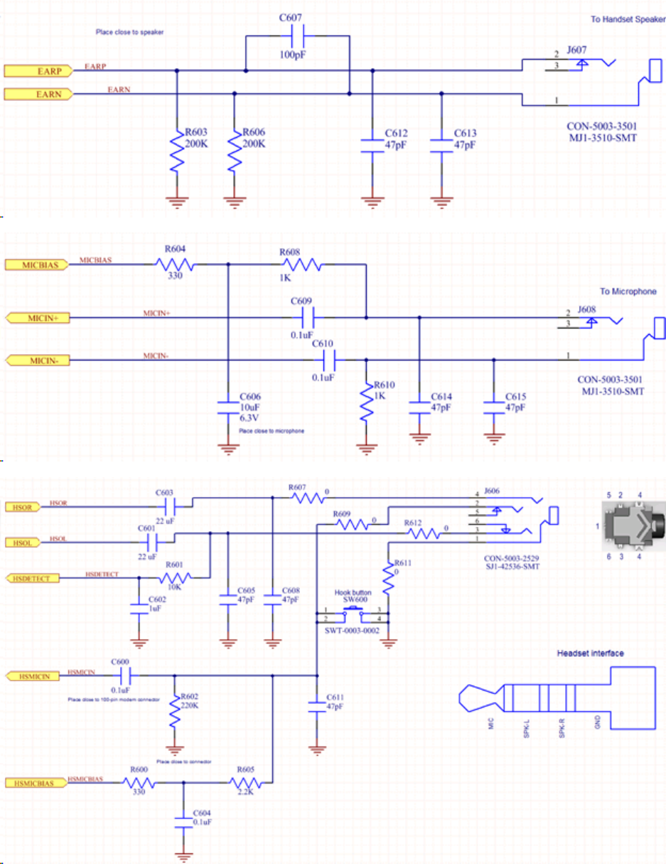
- 27 -
Audio Schematics
- 28 -
Figure 4-6 Audio Reference Design Schematic
- 29 -
Control Connector Signal Descriptions And
Functions
Unless otherwise noted in the following sections, all digital signals will reference the following
specifications:
Parameter Parameter/Conditions Comments MIN TYP MAX UNIT
VIH High level Input voltage 1.17 1.83 V
VIL Low level Input voltage -0.3 0.63 V
VSHYS Schmitt hysteresis voltage 15 mV
ILInput leakage current VDDX = Max
VIN = 0 V to VDDM
200 nA
VOH High level output voltage IOUT = IOH 1.35 1.8 V
VOL Low level output voltage IOUT = IOL 0 0.45 V
IOH High level output voltage 3 mA
IOL Low level output voltage CMOS, at pin rated drive
strength
3 mA
CIN Input Capacitance 5 pF
Module Power (PINS 87, 89, 91, 93, 95, 97, 99)
The HS 3001 module uses a single voltage source of VCC= +3.4 V to 4.4 V.
VBAT Parameter/Conditions
Min
(mA)
Typ
(mA)
Max
(mA)
Units
Main Battery Supply Voltage In Regulation 3.4 4.4 Vdc
Peak Current 1000 µF on Host at Module Connector 600mA 680mA mA
The uplink burst will cause strong ripple on the voltage lines and should be
filtered effectively. We recommend that 1000 µF of capacitance be placed as
close to the modem I/O connector as possible. It should be noted that the input
voltage level should not drop below the minimum voltage rating under any
circumstances, especially during the uplink burst period.

- 30 -
Modem Power-on And Recovery Techniques
The HS 3001 provides module integrators with improved modem power-on and recovery
techniques, while maintaining backwards compatibility to Enabler IIIG integrations. The
addition of an internal power switch and an input power-on logic select pin allows users the
flexibility to maintain backwards compatibility or select different power-on options. This
internal power switch also allows integrators the flexibility of not supplying an external power
switch. Pin 37, previously a reset pin, has been replaced with a device power ON/OFF pin.
This pin controls the internal power switch.
Pin 85 (PSLOGIC) allows users to select the default behavior of the ON/OFF control (Pin 37).
Once power is applied via the internal power switch, Pin 35 (PON) is used like a phone on/off
switch.
Power Switch Logic Detect (Pin 85)
Pin 85 is a hardware input pin used to determine the functionality of the ON/OFF pin (Pin 37).
If Pin 85 is tied to VBAT, Modem ON/OFF (Pin 37) defaults to high when open circuit, and the
modem power switch will be ON. If Pin 85 is left open, Modem ON/OFF (Pin 37) defaults to
low when open circuit and the modem will be OFF (requires ON/OFF to be driven high to
power on).
We do not recommend externally connecting Pin 85 to ground.
ON/OFF (PIN 37)
Pin 37 is the ON/OFF control input for the modem's internal power switch. When it is high,
the modem's power switch will be ON. When it is low, the modem power will be OFF.
In order for the device to power on, pin 35 must be tied low or pulled low after power has
been applied. The device will not power on if it is left floating.
- 31 -
Pin 35 PON (Power On) is a signal input and is the normal method for turning the
modem ON or OFF. However, Pin 35 cannot turn the modem on if Pin 37 is low,
because the modem will not have power applied to it. offdly=0 only affects the
powering off of the device, not power on.
Parameter Min Typ Max Units
Enable Threshold Voltage 1.5 VBAT V
Enable Input Current 1.5 µA
Pulldown approximately 1MΩ.
The modem may not completely shut down/reset even with a mechanical power
switch or this circuit implemented if the modem’s I/O lines have another source of
power that applies voltage to the modem.
To alleviate this situation, make sure that the interface circuitry is set to tri-state
or as an input. If this is not possible, you may need additional hardware to shunt
high impedance lines to ground during these situations.
The un-switched power source must be capable of supporting the inrush current
required by the bulk capacitance. The enable switch can be soft-started via
voltage ramp or modulation to reduce the peak current as needed.
DO NOT USE a Modem Power Switch as a routine shutdown or reset. This
technique for shutting down the modem does not properly deregister the
modem from the network. The carrier may impose penalties if a fleet of
equipment does not routinely follow a proper deregistration process. If you wish
to use this method routinely, you should gracefully detatch from the network
first. This can be done by sending AT$OFF.
Phone On - PON (PIN 35)
This input signals the modem to start and is equivalent to a “phone power button”.
- 32 -
A falling-edge on this Active-Low input will switch-ON or switch-OFF the module. The
firmware controlled OFF function will deregister the modem from the network before
shutting the modem OFF.
This input has a “weak pull-up” resistor internal to the module. If users want the modem to
automatically come on when power is applied, they can tie this line low.
If RTC Sleep is required, then the PON line must be floated to allow the internal resistor to
pull the line high.
Controlling the PON signal must only be performed by an open collector/open drain device. If
controlling this signal from a microprocessor’s I/O pin, the PON can be pulled low when the
I/O is configured to be an output and floated high by reconfiguring the pin to be an input.
The AT$OFFDLY Command controls the OFF Delay. A value of 0 disables the
PON line from turning the module off. 0 is the default value.
To enable the module to switch-OFF via PON you must set AT$OFFDLY to a
value other than 0. The valid range is 100 to 1000 milliseconds.
Internal Power Switch
The modem has an internal power switch that supplies the modem operating power when
ON.
Figure 4-7 Internal Power Switch
- 33 -
Voltage Reference - VREG_MSME1.8 (PIN 77)
To be used as a voltage reference source ONLY. Do not connect current loads to this pin.
When driving external circuitry, this pin should be decoupled to ground with at least a 0.1 µF
capacitor at the output.This pin can be left open if not driving external circuitry. Noise
induced on this pin will affect the performance of the baseband.
USB (PINS 1, 3, 5, 7)
As part of integrated products carrier certification, most carriers require access to
the USB diagnostic port to control the module for testing. If the integrator has not
already brought out the USB interface, it is recommended that the USB interface
be routed to test points on the device, at a minimum. It will be acceptable to
temporary wire a USB connector for purposes of testing during carrier
certification.
5V Tolerant Transceiver
USB Parameter/Conditions Min Typ Max Units
Input Voltage 4.4 4.65 5.25 V
Output voltage High (Driven) 2.8 3.4 3.6 Vdc
Low 0.0 0.1 0.3 Vdc
Transceiver D+/- Leakage Current -2 2 μA
USB D+/- should be routed differentially for 90 ohms impedance. Take care not to
route the USB near sensitive circuitry.
General Purpose Input/Output Interface
GPIO number Pin number
GPIO 1 64
GPIO 2 62
GPIO 3 60
GPIO 4 58
GPIO 5 68
GPIO 6 70
- 34 -
GPIO number Pin number
GPIO 7 66
GPIO 8 72
Each general-purpose signal may be selected as inputs or outputs. The GPIOs can be used
independently as a user-specified function.
Digital I/O Specifications -Baseband Functions
Parameter Comments Min Typ Max Units
VIH High level input voltage CMOS / Schmitt 1.17 1.83 V
VIL low level input voltage CMOS / Schmitt -0.3 0.63 V
VSHYS Schmitt hysteresis voltage 100 mV
IIH Input high leakage current 1 2 No pull-down 1 µA
IIL Input high leakage current 1 2 no pull-up -1 µA
IIHPD Input high leakage current 1 with pull-down 3 30 µA
IILPU Input high leakage current 2 with pull-up -30 -3 µA
VOH High level votage CMOS, at pin rated drive
strength
1.35 1.80 V
VOL Low level votage CMOS, at pin rated drive
strength
0 0.45 V
IOZH 3 State leakage current 2 Logic high output 1 µA
IOZL 3 State leakage current 2 Logic low output -1 µA
IOZHPD 3 State leakage current 2 Logic high output with oull
down
3 30 µA
IOZLPU 3 State leakage current 2 Logic high output with pull-up -30 -3 µA
IOZHKP 3 State leakage current 2 Logic high output with keeper -20 -3 µA
IOZLKP 3 State leakage current 2 Logic high output with keeper 3 20 µA
CIN Input Capacitance 7 pF
RTC Sleep
In this mode, the modem is off except for its Real-Time-Clock. When put into this mode, the
modem can wake itself up at a designated time/interval. See the HS 3001 AT command
manual for details.

- 35 -
Serial Interfaces And Handshake (Pins 11, 13, 15, 17, 19, 21, 23, 25)
The pin naming for TX/RX/RTS/CTS/DTR/DSR/DCD/RI is referenced as a DCE. The DTE
device should match their input pins to the Novatel Wireless M2M outputs and vice-versa.
Additionally, there are AT commands that may need to be executed in order to ensure proper
operation. See the chart below.
9 way D Connector Pin Num-
ber
Signal Signal Dir-
ection
Novatel Wireless M2M Pin Num-
ber
Novatel Wireless M2M AT Com-
mand
1 Carrier Detect (CD) from DCE 19 AT&C
2 Receive Data (RD) from DCE 15
3 Transmit Data (TD) from DTE 21
4 Data Terminal Ready
(DTR)
from DTE 17 AT&D
5 Signal Ground both
6 Data Set Ready (DSR) from DCE 25
7 Request To Send (RTS) from DTE 11 AT+IFC
8 Clear To Send (CTS) from DCE 13 AT+IFC
9 Ring Indicator (RI) from DCE 23
The key features of the UART1 in the modem mode are as follows:
l16C750 compatibility
lBaud rates: 300,600,1200,2400,4800,9600,19200,38400,57600,115200,230400
lSupported data format:
lData bit: 8 bits
lParity bit: none
lStop bit: 1 bit
lHardware flow control RTS/CTS
The HS 3001 module is designed to be used like a DTE device.
Default settings are 8 data, 1 stop, no parity, and 115200. RTS and CTS may be used for
hardware handshaking. DTR may be used to force the modem into AT command mode from
online data mode (See AT Command Document, command AT&D). The serial interface is 1.8 V
logic. By default, hardware handshaking (AT+IFC) is disabled. If the integrator does not wish
to use flow control, disable hardware flow control in the modem using the AT+IFC command.
For a minimal Serial implementation use the following configuration:
lConnect RxData (pin 15) and TxData (pin 21) to the COM port serial data lines.
lSet AT+IFC=0,0 to disable flow control.
Notes:

- 36 -
lTying DTR (pin 17) and RTS (pin 11) to ground to “spoof” flow control will cause the
modem to draw more current.
lWe do not recommend leaving DTR (pin 17) and RTS (pin 11) unconnected. If you are not
going to use these signals, do one of the following:
nPull up DTR (pin 17) and RTS (pin 11) through a 100K resistor; or
nTie RTS (pin 11) to CTS (pin 13), and tie DTR (pin 17) to DSR (pin 25) on the modem
to loopback the signals.
UART 2 (Pins 27, 29)
UART2 supports RX and TX only.
Signal Min Max
VIH - High-level input voltage 1.85V 3.15V
VIL - Low-level input voltage -0.3V 0.95V
VOH - High-level output voltage 2.35V 2.85V
VOL - Low-level output voltage 0V 0.45V
Digital Audio Interface (Pins 12, 14, 16, 18)
This port is only available in Master mode and to be used for PCM digital audio. Below are the
settings for
configuring its operation and the interface specification:
Digital Audio Configuration
The default settings for the digital audio are:
lMode = Master
lMCSI_CLK = 2.048 MHz
lWord Size = 16 Bits
lSync Pulse = 8 KHz
lFrame mode = burst
lClock edge Sync = rising edge
The following command is required to set the unit up in digital audio mode:
AT$voicepth=2
This configures the module to use digital audio instead of analog audio.
Digital Audio Data Format
The 16 bit word is sent MSB first. Data received is also MSB first. No other data manipulation is
done

- 37 -
within the module.
Pin Name Pin Number Signal Direction Description
PCM_RX 12 I Serial Data Input
PCM_TX 18 O Serial Data Output
PCM_CLK 14 IO Serial Clock I/O
PCM_FSYNC 16 IO Frame Synchronization I/O
32 KHz Output (PIN 56)
A 32.768 kHz signal is available as an output from the module. This signal should only be used
as an input to a high impedance device. Additional loads or capacitance on the line may cause
performance issues with the module. If the line is not used, leave floating.
Parameter Comments Min Typ Max Units
Oscillation frequency 32.765 kHz
Duty Cycle 45 50 55 %
Jitter
Cycle to cycle 50 ns
period 10 ns
Analog-to-Digital Inputs (PIN 44 And 74)
The monitoring ADC consists of a successive approximation 10–bit analog–to–digital converter
(ADC).
ADC Specifications
Parameter Min Typ Max Units Comments
Resolution 10-bit
Full scale error 2.5%
Number of
input channels
2
Full scale input
range
GND 1.8 V
Input res-
istance
1.5 kΩ S/H resistance
Input capa-
citance
12.4 pF S/H capacitor
- 38 -
Handset Microphone Input (PINS 65, 67)
Parameter Test Conditions Min Typ Max Units Notes
Full scale input
voltage
voltage across either MIC 1P and MIC1N, MIC2P and
MIC2N
0.89 1.00 1.12 Vrms ± 1dB level error
Input impendence Difference input impedance 16 20 24 kΩ
Input impendence Single ended input impedance 8 10 12 kΩ
Input offset voltage 5 5 mV
Input capacitance At each pin of all inputs 5 pF
Handset Microphone BIAS Output (PINS 53, 63)
Parameter Comments Min Typ Max Units
MIC bias output voltage 1.8 V
MIC bias output current 1.5 mA
MIC bias voltage accuracy Minimum load -3 +3 %
MIC bias output voltage load regulation 30 Ω
Handset Speaker Output (PINS 71, 73)
Parameter Test Conditions Min Typ Max Units Notes
DAC to
EAROP/EARON full-
scale output
f = 1.02 Hz, 0
dBm
1.11 1.25 1.40 Vrms ± 1 dB level error
EAROP/EARON
output power, 4%
or less THD+N
f = 498 Hz, 0 dBm 38.5 48.8 61.3 mW 22 to 20 kHz
measurement BW
Output DC level,
EAR1OP and
EAR1ON with
respect to VSS
Input = .999 dBm 1.03 1.05 1.07 V
Headset Microphone Input (PIN 55)
Parameter Test Conditions Min Typ Max Units Notes
Full scale input voltage voltage across pin 55 and ground 0.89 1.00 1.12 Vrms ± 1dB level error
Input impendence Single ended input impedance 8 10 12 kΩ
Input offset voltage 5 5 mV
Input capacitance At each pin of all inputs 5 pF

- 39 -
Headset Speaker Output Left And Right (PINS 57, 59)
Parameter Test Conditions Min Typ Max Units Notes
Both modes - HPH_LP and HPH_RN configured single ended, analog volume control = 0 dB
DAC to HPH_LP and HPH_RN
fullscale output
f = 1.02 kHz, 0 dBm 0.531 0.595 0.668 Vrms
Output DC level, HPH_LP and
HRH_RN wih respect to VSS
Input = 0.999 dBm 1.03 1.05 1.07 V
Output impedence 0.5 Ω
Voice Mode - HPH_LP and / or HPH_RN configured single ended, analog volume control = 0 dB
HPH_LP and HPH_RN output
power, 4% or less THD+N
f = 1.02 kHz, 0 dBm 17.6 22.1 27.9 mW 22 to 20 kHz
meas-
urement
bandwidth
DAC to HPH_LP and HPH_RN
output noise level
Input = 0.999 dBm, Fs = 8 kHz or
16 kHz, A-weighted
106 µVrms
Both modes - HPH_LP and HPH_RN configured differential (HPH_LP/HPH_RN), analog volume control = 0 dB
DAC to HPH_LP and HPH_RN
fullscale output
f = 1.02 kHz, 0 dBFS, 32 Ω load 1.06 1.19 1.34 Vrms
DAC to HPH_LP/HPH_RN gain
error relative to gain @ -3
dBFS
f = 1.02 kHz, -60 dBFS -1.2 1.2 dB Linearty
spot check
Output DC level, HPH_P and
HPH_N with respect to VSS
Input = .999 dBFs 1.03 1.05 1.07 V
Output impedence 1.0 Ω
Voice Mode - HPH_LP and / or HPH_RN configured differential (HPH_LP/HPH_RN), analog volume control = 0 dB
HPH_LP/HPH_RN output
power, 4% or less THD+N
f = 498 Hz, -3 dBFS, 32 Ω 17.6 22.1 27.9 mW 22 to 20 kHz
meas-
urement
bandwidth
DAC to HPH_LP/HPH_RN out-
put noise level
Input = 0.999 dBFS, Fs = 8 kHz, A-
weighted
212 µVrms 22 to 20 kHz
meas-
urement
bandwidth
Headset Detect (PIN 47)
The headset detect signal is an active low signal. The signal is low when a headset is inserted.
Circuit Protection
Other than very low level ESD protection within the module’s integrated circuits, the module
does not have any protection against ESD events or other excursions that exceed the
specified operating parameters. Only the USB port has onboard ESD/transient protection. We
do not recommend using additional external transient protection for this port as it will cause
too much capacitance on the lines.

- 40 -
Generally, ESD protection (typically TVS/Transzorb devices) should be added to all signals
that leave the host board. This includes VBAT/VCC.
Series resistors (typically 47 ohms) can also be added in series with data lines to limit the peak
current during a voltage excursion.
It is your responsibility to protect the module from electrical disturbances and
excursions that exceed the specified operating parameters.

- 42 -
USB Driver Installation (Windows XP)
These instructions illustrate how to correctly install the USB drivers in Windows XP using the
Novatel Wireless M2M Driver Setup Utility.
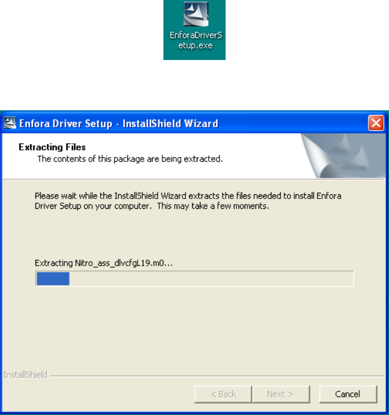
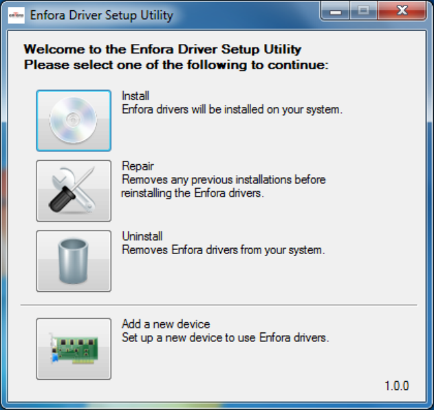
1. Run the Novatel Wireless M2M Driver Setup Utility by double-clicking the Novatel
Wireless M2MDriverSetup executable file.
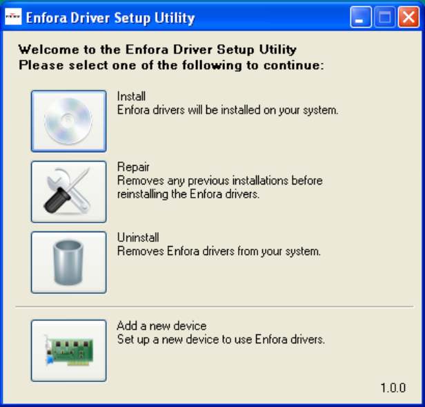
The Novatel Wireless M2M Driver Setup Utility Extraction window opens.
Figure 5-1 Novatel Wireless M2M Driver Setup Utility Extraction
Once the contents have been extracted to memory, the Welcome Window opens.
- 43 -
Figure 5-2 Novatel Wireless M2M Driver Setup Utility Welcome
2. To install the drivers, select Install.
The Novatel Wireless M2M Driver Setup Utility Window opens.
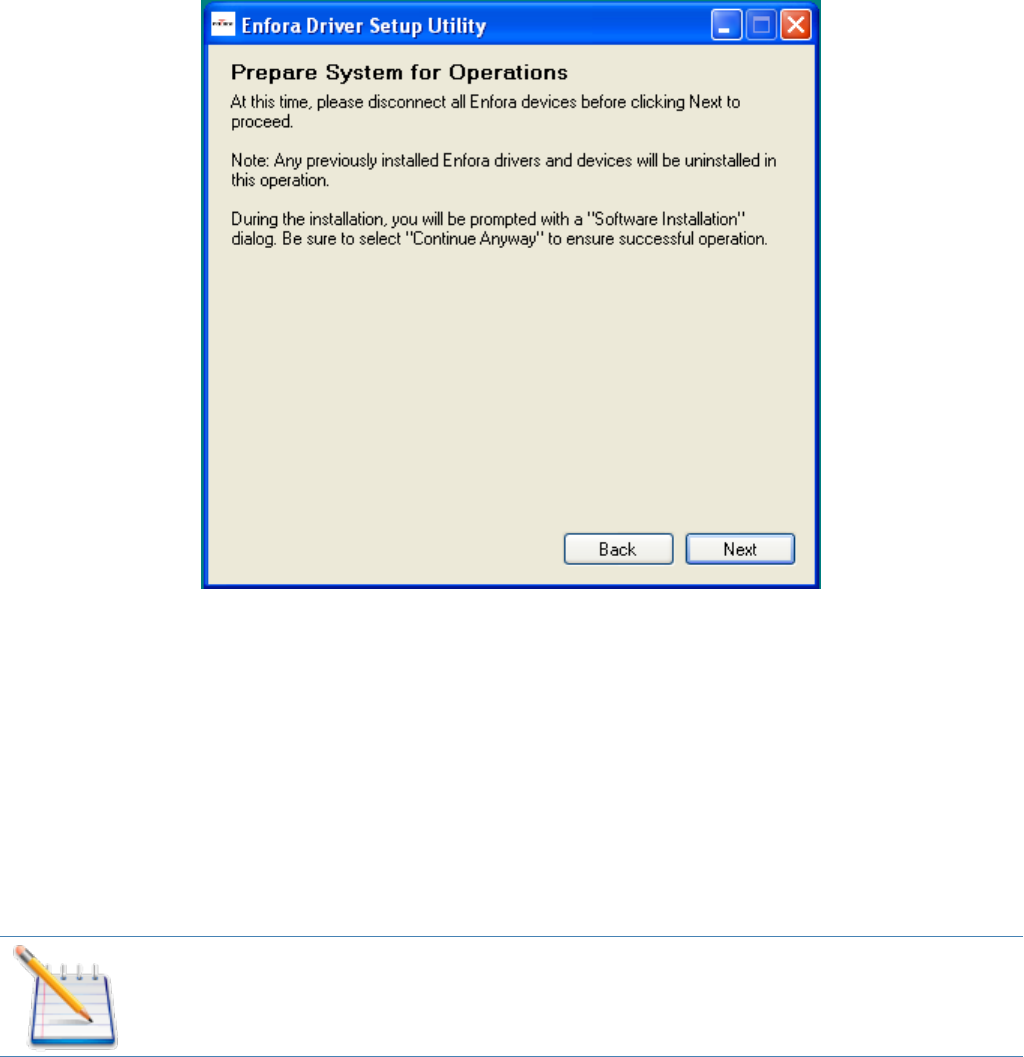
- 44 -
Figure 5-3 Novatel Wireless M2M Driver Setup Utility Prepare System Window
3. Select Next to continue.
The Novatel Wireless M2M Driver Setup Utility Installation Window opens while
the system installs the drivers.
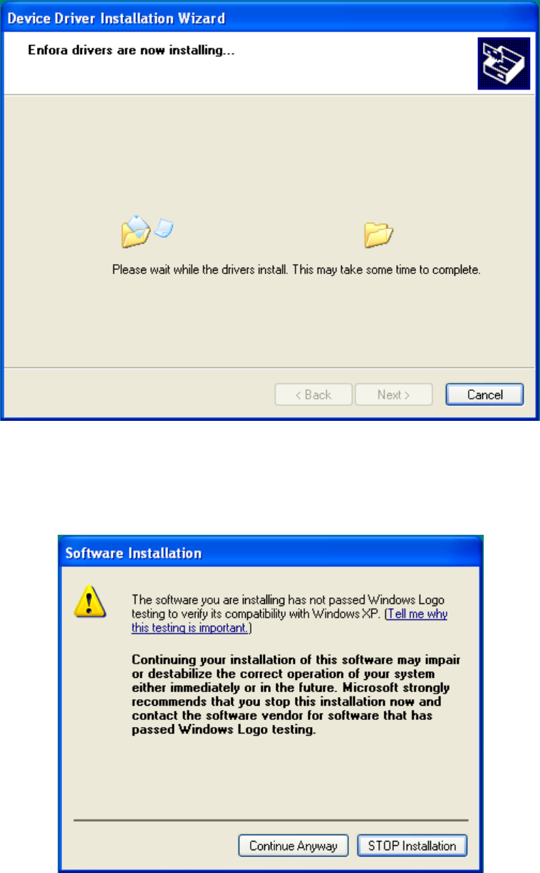
4. Disconnect any Novatel Wireless M2M devices.
Previous drivers will be removed during this phase.
During the installation, your computer's display may freeze and appear non-
responsive. If this occurs, allow the computer to continue working. After 2-3
minutes, the display and installer will resume normal behavior.
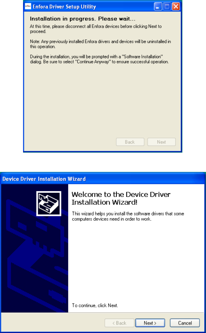
- 45 -
Figure 5-4 Novatel Wireless M2M Driver Setup Utility Installation Window
Figure 5-5 Novatel Wireless M2M Driver Setup Utility Driver Installation
5. When prompted to install the device driver, select Next.
- 46 -
Figure 5-6 Novatel Wireless M2M Driver Setup Utility Driver Installation Progress
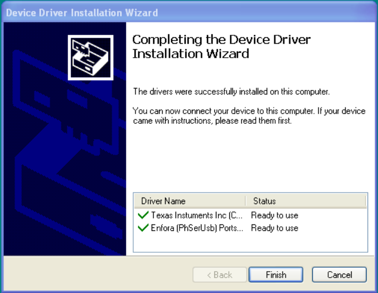
You may see the following warning message:
Figure 5-7 Windows Security Window
- 47 -
6. Click Continue Anyway.
When installation of the USB drivers is complete, the Completion window opens.
Figure 5-8 Novatel Wireless M2M Driver Setup Utility Driver Install Completion Window
7. Click Finish.
When the installation is complete, the list of attached devices will appear within
the Attached Devices Window.
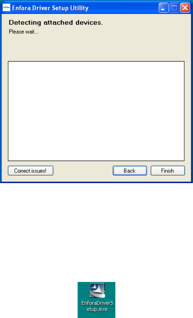
- 48 -
Figure 5-9 Novatel Wireless M2M Driver Setup Utility Attached Devices Window
USB Driver Installation (Windows 7)
These instructions illustrate how to correctly install the USB drivers in Windows 7 using the
Novatel Wireless M2M Driver Setup Utility.
1. Run the Novatel Wireless M2M Driver Setup Utility by double-clicking the Novatel
Wireless M2MDriverSetup executable file.
The Novatel Wireless M2M Driver Setup Utility Welcome window opens.
- 49 -
Figure 5-10 Novatel Wireless M2M Driver Setup Utility Welcome Window
Once the contents have been extracted to memory, the Driver Setup Window
opens.
- 50 -
Figure 5-11 Novatel Wireless M2M Driver Setup Utility Preparation Window
2. To install the drivers, click Install.
The Novatel Wireless M2M Driver Setup Utility Prepare System Window opens.
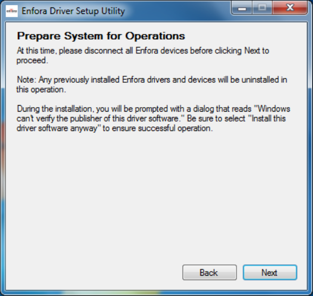
- 51 -
Figure 5-12 Novatel Wireless M2M Driver Setup Utility Installation Window
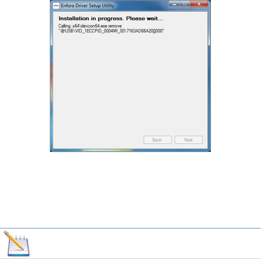
3. Select Next to continue.
The Novatel Wireless M2M Driver Setup Utility Installation Window opens while
the system installs the drivers.
4. Disconnect any Novatel Wireless M2M devices.
Previous drivers will be removed during this phase.
During the installation, your computer's display may freeze and appear non-
responsive. If this occurs, allow the computer to continue working. After 2-3
minutes, the display and installer will resume normal behavior.
- 52 -
Figure 5-13 Novatel Wireless M2M Driver Setup Utility Driver Installation
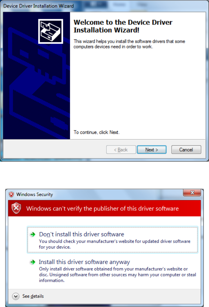
5. When prompted to install the device driver, select Next.
Figure 5-14 Windows Security Window
6. Select Install this driver software anyway.
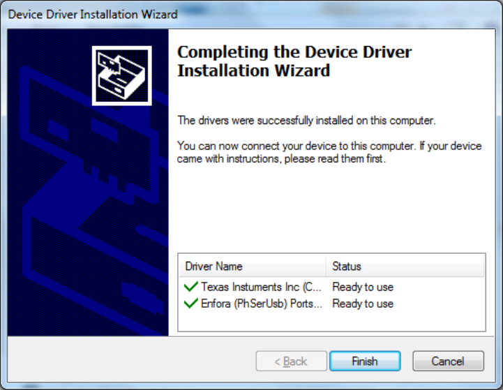
- 53 -
During the driver install phase, you may be prompted to continue or stop installation due to
potential compatibility issues.
Figure 5-15 Novatel Wireless M2M Driver Setup Utility Driver Install Completion Window
When installation of the USB drivers is complete, the Completion window opens.
7. If there are no errors, click Finish.
8. If the status displays an issue, click Correct issues!
9. At the "OK to apply fix" prompt, click Yes.
- 54 -
Figure 5-16 Novatel Wireless M2M Driver Setup Utility Attached Devices Window
Figure 5-17 Novatel Wireless M2M Driver Setup Utility Apply Fix Window
When the installation is complete, the list of Attached Devices appears within the
Novatel Wireless M2M Driver Setup Utility Attached Devices window.
- 55 -
Figure 5-18 Novatel Wireless M2M Driver Setup Utility Attached Devices Window