Novatel Wireless CNN0301 1XRTT Multi-Band M2M OEM Module User Manual CNN0301IG001 HS 3001
Novatel Wireless Inc. 1XRTT Multi-Band M2M OEM Module CNN0301IG001 HS 3001
Contents
- 1. User Manual
- 2. Integration Guide
User Manual

HS 3001
Integration Guide
CNN0301IG001
Version:DRAFT 0.1
10 May, 2012
General
TERMS OF USE OF NEW MATERIALS - PLEASE READ CAREFULLY
From time to time, Enfora, in its sole discretion, may make available for download on its website
(www.enfora.com), or may transmit via mail or email, updates or upgrades to, or new releases of, the
firmware, software or documentation for its products (collectively, 'New Materials'). Use of such New
Materials is subject to the terms and conditions set forth below, and may be subject to additional terms
and conditions as set forth in Enfora's Technical Support Policy (posted on its website) and/or any written
agreement between the user and Enfora.
All New Materials are provided AS IS. Enfora makes no warranty or representation with respect to the
merchantability, suitability, functionality, accuracy or completeness of any such New Materials. The user of
such New Materials assumes all risk (known or unknown) of such use. Enfora reserves all rights in such
New Materials. The user shall have only a revocable and limited license to use such New Materials in
connection with the products for which they are intended. Distribution or modification of any New
Materials without Enfora's consent is strictly prohibited.
IN NO EVENT WILL ENFORA BE RESPONSIBLE FOR ANY INCIDENTAL, INDIRECT, CONSEQUENTIAL OR
SPECIAL DAMAGES AS A RESULT OF THE USE OF ANY NEW MATERIALS. ENFORA'S MAXIMUM LIABILITY
FOR ANY CLAIM BASED ON THE NEW MATERIALS SHALL NOT EXCEED FIFTY U.S. DOLLARS ($50).
- ii -
Copyright
© 2012 Enfora, Inc. All rights reserved. Complying with all applicable copyright laws is the responsibility of
the user. Without limiting the rights under copyright, no part of this document may be reproduced, stored
in or introduced into a retrieval system, or transmitted in any form or by any means (electronic,
mechanical, photocopying, recording or otherwise), or for any purpose, without the express written
permission of Enfora, Inc.
Enfora and the Enfora logo are either registered trademarks or trademarks of Enfora, Inc. in the United
States.
251 Renner Pkwy
Richardson, TX 75080 USA
Phone: (972) 633-4400
Fax: (972) 633-4444
Email: info@enfora.com
www.enfora.com
- iii -
WARRANTY INFORMATION
[Revised: 11/11/2010]
This warranty applies to (a) products sold directly by Enfora, unless a different warranty is specified in a
written agreement between Enfora and the purchaser; and (b) products sold to end users through a
distributor authorized by Enfora, but only where the authorized distributor does not provide a separate
warranty on such products, and Enfora has agreed to provide this warranty to such end users. If you
purchased the product from an authorized distributor, please check whether this warranty from Enfora, or
a separate warranty from the distributor, applies to your purchase. This warranty does not apply to any (i)
accessories or batteries for the products; or (ii) demonstration samples or prototypes of the products.
Unless otherwise provided in a written agreement between Enfora and the purchaser, all such accessories,
batteries, samples or prototypes are provided by Enfora AS IS without any warranty of any kind.
Enfora warrants to the original purchaser of the product from Enfora or its authorized distributor (as
applicable) that, for a period of one (1) year from the date of shipment of the product from Enfora, the
product hardware will be substantially free from defects in material or workmanship under normal
operation, and the product firmware will perform substantially in accordance with the product
documentation provided by Enfora. Enfora does not warrant that (a) the product hardware or firmware
will meet the purchaser's requirements; (b) the operation of the product hardware or firmware will be
uninterrupted or error-free; or (c) the product, when integrated in, or combined with, other products or
software not supplied by Enfora, will continue to perform substantially in accordance with the product
documentation. This limited warranty is for the benefit of the original purchaser, and is not transferable.
During the warranty period, Enfora, at its expense and in its sole discretion, will repair the product, or
replace the product with a corresponding or equivalent product, if it is determined to have a covered
defect, provided that the purchaser first notifies Enfora (directly or through its authorized distributor from
which the product was purchased) of any such defect, furnishes Enfora with a proof of purchase (if
required), requests and obtains a return merchandize authorization (RMA) number from Enfora, and
returns the product under that RMA to Enfora (or, at Enfora's option, to its authorized distributor), with the
shipping charges being prepaid by purchaser. If, upon reasonable examination of the returned product,
Enfora does not substantiate the defect claimed by purchaser, or determines that the defect is not covered
under this limited warranty, Enfora will not be required to repair or replace the product, but may instead
reship the product to the purchaser (or, at Enfora's option, to its authorized distributor where the product
can be made available to purchaser), in which case the purchaser shall be responsible for paying Enfora's
cost for reshipping the product to purchaser (or to Enfora's authorized distributor), and Enfora's usual
charges for unpacking, testing, and repacking the product for reshipment to purchaser (or to Enfora's
authorized distributor).Purchaser shall bear the risk of loss or damage in transit to any product returned by
purchaser to Enfora, or any returned product not found to be defective or covered under this warranty, and
reshipped by Enfora to purchaser (or to Enfora's authorized distributor). In the event Enfora repairs or
- 4 -
replaces a defective product covered by this limited warranty, the repaired or replacement product will be
covered under this limited warranty for the remainder of the original warranty period on the defective
product, or a period of ninety (90) days, whichever is longer. If Enfora is unable to repair or replace a
defective product covered by this limited warranty, Enfora will provide to purchaser a credit or a refund
(at Enfora's option) of the original purchase price (excluding taxes and shipping charges). Any returned and
replaced product, or any product for which Enfora has furnished a credit or a refund, becomes the
property of Enfora.
Enfora shall not have any obligation to provide any firmware bug fixes, upgrades or new releases except as
may be necessary to correct any covered defect of which purchaser notifies Enfora in writing during the
warranty period. Enfora, from time to time and in its sole discretion, may make available for download on
its website (www.enfora.com), or may provide via email, certain firmware bug fixes, upgrades or new
releases for the product. Download and use of any such bug fixes, upgrades or new releases is subject to all
of the applicable terms and conditions of Enfora's technical support policy as posted and updated on its
website.
Enfora shall have no obligation under this limited warranty for (a) normal wear and tear; (b) the cost of
procurement of substitute products; or (c) any defect that is (i) discovered by purchaser during the
warranty period but for which purchaser does not request an RMA number from Enfora, as required
above, until after the end of the warranty period, (ii) caused by any accident, misuse, abuse, improper
installation, handling or testing, or unauthorized repair or modification of the product, (iii) caused by use of
any materials not supplied by Enfora, or by use of the product other than in accordance with its
documentation, or (iv) the result of electrostatic discharge, electrical surge, fire, flood or similar causes.
The purchaser (or its customers, as applicable) shall be solely responsible for the proper configuration,
testing and verification of the Enfora product prior to deployment in the field, and for ensuring that any
end user product or system into which the Enfora product is integrated or incorporated operates as
intended and meets the requirements of purchaser (or its customers). Enfora shall have no responsibility
whatsoever for the integration, configuration, testing, verification, installation, upgrade, support or
maintenance of any such end user product or system, or for any liabilities, damages, costs or expenses
associated therewith.
ENFORA'S SOLE RESPONSIBILITY AND PURCHASER'S SOLE REMEDY UNDER THIS LIMITED WARRANTY
SHALL BE FOR ENFORA TO REPAIR OR REPLACE THE PRODUCT (OR IF REPAIR OR REPLACEMENT IS NOT
POSSIBLE, PROVIDE A CREDIT OR REFUND OF THE PURCHASE PRICE) AS PROVIDED ABOVE. ENFORA
EXPRESSLY DISCLAIMS ALL OTHER WARRANTIES OF ANY KIND, EXPRESS OR IMPLIED, INCLUDING
WITHOUT LIMITATION ANY IMPLIED WARRANTIES OF NON-INFRINGEMENT, MERCHANTABILITY,
SATISFACTORY PERFORMANCE AND FITNESS FOR A PARTICULAR PURPOSE. IN NO EVENT SHALL ENFORA
BE LIABLE FOR ANY INDIRECT, SPECIAL, EXEMPLARY, INCIDENTAL OR CONSEQUENTIAL DAMAGES
(INCLUDING WITHOUT LIMITATION LOSS OR INTERRUPTION OF USE, DATA, REVENUES OR PROFITS)
- 5 -
RESULTING FROM A BREACH OF THIS WARRANTY OR BASED ON ANY OTHER LEGAL THEORY, EVEN IF
ENFORA HAS BEEN ADVISED OF THE POSSIBILITY OR LIKELIHOOD OF SUCH DAMAGES.
Some jurisdictions may require a longer warranty period than specified above and, accordingly, for
products sold in those jurisdictions the applicable warranty period shall be extended as required under the
laws of those jurisdictions. Furthermore, some jurisdictions may not allow the disclaimer of implied
warranties or the exclusion or limitation of incidental or consequential damages, so the above disclaimer,
limitation or exclusion may not apply to products sold in those jurisdictions. This limited warranty gives the
purchaser specific legal rights and the purchaser may have other legal rights that vary from jurisdiction to
jurisdiction.
This limited warranty shall be governed by the laws of the State of Texas, United States of America,
without regard to conflict of laws principles. This limited warranty shall not be governed in any respect by
the United Nations Convention on Contracts for the International Sale of Goods.
Regulatory Compliance
FCC CERTIFICATION
Enfora certifies that the Enabler HS 3001 CDMA Radio Module (FCC ID: MIVCNN0301) complies with the
RF requirements applicable to broadband PCS equipment operating under the authority of 47 CFR Part 24,
Subpart E and Part 22 of the FCC Rules and Regulations. This certification is contingent upon installation,
operation and use of the Enabler HS 3001 module and its host product in accordance with all instructions
provided to both the OEM and end user. When installed and operated in a manner consistent with the
instructions provided, the Enabler HS 3001 module meets the maximum permissible exposure (MPE) limits
for general population / uncontrolled exposure at defined in Section 1.1310 of the FCC Rules and
Regulations.
The Enabler HS 3001 module is designed for use in a variety of host units, "enabling" the host platform to
perform wireless data communications. However, there are certain criteria relative to integrating the
modem into a host platform such as a PC, laptop, handheld, monitor and control unit, etc. that must be
considered to ensure continued compliance with FCC compliance requirements.
In order to use the Enabler HS 3001 module without any additional FCC certification the installation must
meet the following conditions:
lThe system antenna(s) connected to the Enabler HS 3001 module must be installed to provide at
least 20cm separation from the human body during normal operation.
lThe system antennas must not be co-located with any other transmitter or antenna.
- 6 -

lThe system antenna(s) used with the Enabler HS 3001 module must not exceed the following levels:
lBand Class 0: the maximum gain is 2.2dBi.
lBand Class 1: the maximum gain is 8dBi.
If any of these conditions are not met then additional information should be sought from the FCC or an FCC
qualified test laboratory.
The system user manuals and other documentation must also include appropriate caution and warning
statements and information.
FCC NOTICE TOUSERS
Enfora has not approved any changes or modifications to this device by the user. Any changes or
modifications could void the users authority to operate the device. See 47 CFR Sec. 15.21. The device
complies with part 15 of the FCC rules. Operation is subject to the following two conditions: (1) This device
may not cause harmful interference, and (2) this device must accept any interference received, including
interference that may cause undesired operation. See 47 CFR Sec. 15.19.
This equipment has been tested and found to comply with the limits for a Class B digital device, pursuant to
part 15 of the FCC rules. These limits are designed to provide reasonable protection against harmful
interference in a residential installation. This equipment generates, uses, and can radiate radio frequency
energy and, if not installed and used in accordance with the instructions, may cause harmful interference
to radio communications. However, there is no guarantee that interference will not occur in a particular
installation. If this equipment does cause harmful interference to radio or television reception, which can
be determined by turning the equipment off and on the user is encouraged to try to correct the
interference by one or more of the following measures:
lReorient or relocate the receiving antenna.
lIncrease the separation between the equipment and receiver.
lConnect the equipment into an outlet on a circuit different from that to which the receiver is con-
nected.
lConsult the dealer or an experienced radio/TV technician for help.
If the FCCID of the module is not visible when installed in the host platform, then a permanently attached
or marked label must be displayed on the host unit referring to the module.
The label should contain wording such as:
Contains FCC ID: MIVCNN0301
This device complies with Part 15 of the FCC Rules. Operation is subject to the following two conditions:
(1) This device may not cause harmful interference, and (2) This device must accept any interference
received, including interference that may cause undesired operation.
ROHS COMPLIANCE
- 7 -
As a part of Enfora’s corporate policy of environmental protection, Enfora takes every step to ensure that
the HS 3002 modules are designed and manufactured to comply to the European Union Directive
2002/95/EC for the Restriction of Hazardous Substances (RoHS).
- 8 -
Important Safety Information
The following information applies to the devices described in this manual. Always observe all standard and
accepted safety precautions and guidelines when handling any electrical device.
lSave this manual: it contains important safety information and operating instructions.
lDo not expose the HS 3001 product to open flames.
lEnsure that liquids do not spill onto the devices.
lDo not attempt to disassemble the product: Doing so will void the warranty. This product does not
contain consumer-serviceable components.
Disclaimer
The information and instructions contained within this publication comply with all FCC, GCF, PTCRB,
R&TTE, IMEI and other applicable codes that are in effect at the time of publication. Enfora disclaims all
responsibility for any act or omissions, or for breach of law, code or regulation, including local or state
codes, performed by a third party.
Enfora strongly recommends that all installations, hookups, transmissions, etc., be performed by persons
who are experienced in the fields of radio frequency technologies. Enfora acknowledges that the
installation, setup and transmission guidelines contained within this publication are guidelines, and that
each installation may have variables outside of the guidelines contained herein. Said variables must be
taken into consideration when installing or using the product, and Enfora shall not be responsible for
installations or transmissions that fall outside of the parameters set forth in this publication.
Enfora shall not be liable for consequential or incidental damages, injury to any person or property,
anticipated or lost profits, loss of time, or other losses incurred by Customer or any third party in
connection with the installation of the Products or Customer's failure to comply with the information and
instructions contained herein.
- 9 -

Table of Contents
1 Introduction/Overview 1
1.1 Product Overview 1
1.2 HS 3001 Product Specifications 1
1.3 Reference Documents 4
1.3.1 HS 3001 Product Documentation 4
1.4 Typical Usage 5
1.5 Contacting Enfora 5
2 Module Power 6
2.1 Operating Power 6
2.1.1 Typical Input Current 6
2.1.2 CDMA Operation Input Current 6
3 Interfaces 7
3.1 Module Mounting to Host Board (Reference) 7
3.2 Connectors 10
3.3 RF Connection Options 11
3.3.1 RF Board-to-Board Connector Option 11
3.4 I/O Connector Pin Assignments 11
4 Hardware Design Guidelines 15
4.1 General Design Guidelines for Utilizing HS 3001 Modules 15
4.1.1 Advanced Tips for an RF Friendly Layout 15
4.1.2 Audio Reference Design 20
4.2 Control Connector Signal Descriptions and Functions 22
4.2.1 Module Power (PINS 87, 89, 91, 93, 95, 97, 99) 23
4.2.2 Modem Power-on and Recovery Techniques 23
4.2.3 Power Switch Logic Detect (Pin 85) 23
4.2.4 ON/OFF (PIN 37) 24
- x -

4.2.5 Phone On - PHON (PIN 35) 25
4.2.6 Internal Power Switch 26
4.2.7 Voltage Reference - VRIO_MSME1.8 (PIN 77) 26
4.2.8 USB (PINS 1, 3, 5, 7) 27
4.2.9 General Purpose Input/Output Interface 27
4.2.10 RTC Sleep 28
4.2.11 Serial Interfaces and Handshake (Pins 11, 13, 15, 21) 28
4.2.12 Digital Audio Interface (PINS 12, 14, 16, 18) 29
4.2.13 32 KHZ Output (PIN 56) 30
4.2.14 Analog-to-Digital Inputs (PIN 44 and 74) 30
4.2.15 Handset Microphone Input (PINS 65, 67) 31
4.2.16 Handset Microphone BIASOutput (PIN 63) 31
4.2.17 Handset Speaker Output (PINS 71, 73) 31
4.2.18 Headset Microphone Input (PIN 55) 32
4.2.19 Headset Speaker Output Left and Right (PINS 57, 59) 32
4.2.20 Headset Detect (PIN 47) 33
4.3 Circuit Protection 33
- xi -
1 Introduction/Overview
1.1 Product Overview
The HS 3001 modem is a compact, wireless OEM module that utilizes the Code Division Multiple Access
CDMA international communications standard to provide two-way wireless capabilities. The HS 3001
module is a fully approved CDMA device, enabling application-specific, two-way communication and
control.
The small size of the HS 3001 module allows it to be integrated easily into the application and packaging.
Figure: 1 - HS 3001 Module
1.2 HS 3001 Product Specifications
The following table lists the main features and specifications of the HS 3001 Module.
Physical Dimensions and Weight
Size (L x W x H) 28.0 mm x 25.0 mm x 4.50 mm
Weight 4 grams
- 1 -

Interfaces
Host Interface Serial Interface
Data input/output interface 100 position 0.4mm pitch connector (Molex P/N 55909-1074)
Primary serial port V.24 protocol, 1.8V levels, UART implementation, Hardware flow
control
USB port USB serial port and USB Debug (USB Debug is Enfora Use only)
GPIO Up to 8 GPIO
Audio Analog and Digital audio
Voice Supports Handset and Headset audio interfaces
Antenna Interface B2B Spring contact
Command protocol Enfora Packet API, CDMA AT command set
Reference clock 32kHz output reference clocks (accessible via 100-pin connector)
ADC 2 ADC inputs
Logic
lUART1
lPCM
lDigital Audio
lGPIO
lPWON
lPower Control
1.8 V
UART2 2.85 V
USB 3.3 V
VBUS 5.0 V
Mic Bias Out 1.8 V @ 1.5 mA max.
Audio Mic Inputs 1.0 Vp-p ±12%
Ear Audio Out TBD
Headset Out L&R TBD
Power
Electrical power Electrical power 3.3 to 4.4 Vdc (vbat)
Supply Vripple must be less than 25mV across all frequencies.
- 2 -

Peak currents and average power
dissipation
Refer to the Operating Power table in the Technical Specifications
for peak currents and average power dissipation for various
modes of operation.
Radio Features
Frequency bands BC0-800 MHz –US Cell, BC1-1900 MHz – US PCS
Radio Mode CDMA 1xRTT, 153 kbps FL/RL
Chipset Qualcomm QSC1110
Packet Data Transfer
Protocol CDMA 1xRTT (153 kbps UL and DL)
Short Message Services Text, PDU, MO/MT, Cell Broadcast
Application Interface
Host Protocol AT commands, PPP FOTA and UDP API available in future release.
Internal Protocols PPP, UDP PAD UDP API, TCP API and TCP PAD available in future
release.
Physical Interface UART, USB
Audio Interface Digital, Analog, Headset and Handset interfaces.
Audio Features Handset Microphone biasing
Headset Microphone biasing
Headset Plug/Unplug detection
Handset microphone input (MICIN, MICIP pins)
Headset microphone input (HSMIC pin)
Outputs Handset earphone outputs (EARP, EARN pins)
Headset 32 Ω stereo outputs (HSOL, HSOR pins)
Mechanical: Operational
Operational vibration, sinusoidal TBD
- 3 -

Operational vibration, random TBD
Mechanical: Storage and Trans-
portation
Transportation vibration, packaged ASTM D999
Drop, packaged ASTM D775 method A, 10 drops
Shock, un-packaged TBD
Drop, un-packaged TBD
Environmental
CDMA Sensitivity (Typical) ≤ -108 dBm
Compliant Operating Temp. -20 °C to 60 °C (CDMA Spec Compliant)
Operating Temperature. -30 °C to 70 °C
Storage Temperature -40 °C to 85 °C
Humidity Up to 95% non condensing
Emissions FCC 47 CFR Parts 2,15,22 & 24
Regulatory
Agency approvals FCC Certification
1.3 Reference Documents
1.3.1 HS 3001 Product Documentation
1.3.1.1 Manuals
lCNN0301AT001 - HS 3001 AT Command Reference
lCNN0301TG001 - HS 3001 Transition Guide
lENF0000SD001 - HDK Guide
- 4 -

1.4 Typical Usage
A variety of applications can use the HS 3001 module for transmitting/receiving data/voice, such as:
lAutomated Meter Reading (AMR)
lPoint of Sale Applications
lE-mail and Internet access
lAutomated Vehicle Location (AVL)
lMachine to Machine communication (M2M)
lTelematics
lTelemetry
lWireless Security
lSmart Phones
lTelemedicine
1.5 Contacting Enfora
For technical support and customer service dealing with the modem itself, contact the company where you
purchased the product. If you purchased the product directly from Enfora, visit the SUPPORT page on the
Enfora website. www.enfora.com
- 5 -

2 Module Power
2.1 Operating Power
2.1.1 Typical Input Current
Test Conditions:
Typical Results @ 3.6 V, 20 deg C, with 1000 μF at connector input on VBAT and RF terminated into a 50Ω
resistive load.
Traffic Data Rate: Full
BC0 Ch = 550
BC1 Ch = 550
2.1.2 CDMA Operation Input Current
Band Mode Low Nom/Avg High/Peak Units
Average Peak
MAX
BC1 550mA
BC0 490mA
MIN
BC1 130mA
BC0 115mA
- 6 -
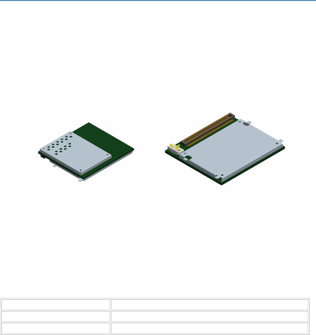
3 Interfaces
Image TBD
Figure: 2 - Front of Module (Board-to-Board RF Conn. Version)
Image TBD
Figure: 3 - Pin 1 Reference, 100-Pin I/O Connector
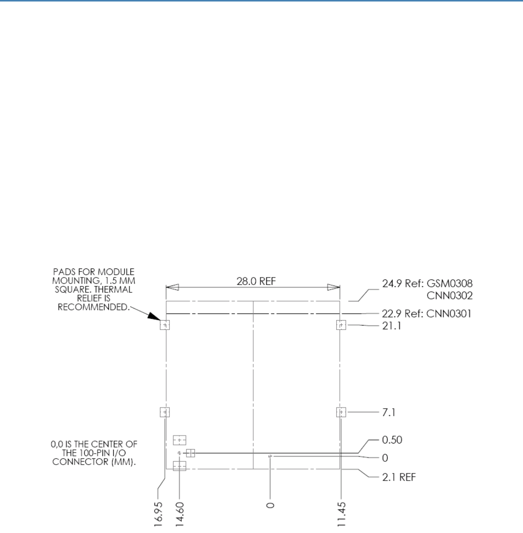
3.1 Module Mounting To Host Board (Reference)
The module provides mounting tabs that must be soldered to a PCB. These tabs provide circuit grounding
for the module.
Figure: 4 - Host Board Layout
- 7 -
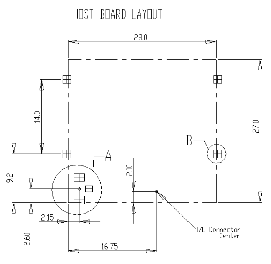
Figure: 5 - Module Mounting
- 8 -
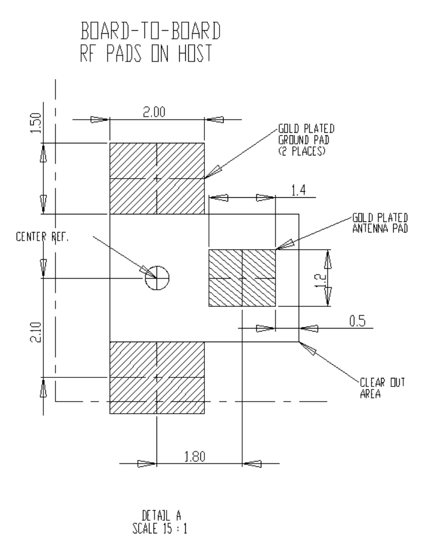
Figure: 6 - Host Pads for Board-To-Board RF Connector
- 9 -
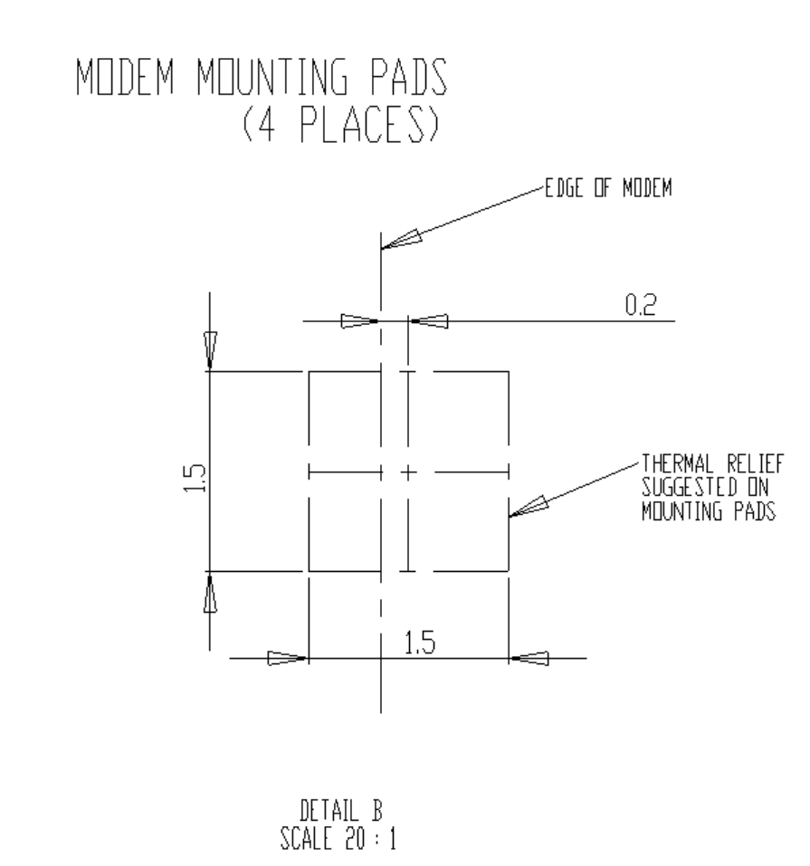
Figure: 7 - Modem Mounting Pads
3.2 Connectors
On The Modem: 100-Pin I/O Connector, Plug, SMT, Dual Row, 0.4 mm Pitch
- 10 -

lEnfora PN = CON-1040-0100
lMolex PN = 55909-1074
On The Host: 100-Pin I/O Connector, Socket, SMT, Dual Row, 0.4 mm Pitch (Mate to module)
lEnfora PN = CON-1040-0101
lMolex PN = 51338-1074
The mated height of the two connectors is 1.50 mm.
3.3 RF Connection Options
3.3.1 RF Board-to-Board Connector Option
On The Modem:
Enfora PN = CON-0009-0006
Sunridge PN = MCE-15A-G01
On The Host PCB:
No connector required.
3.4 I/O Connector Pin Assignments
The following table shows the pin assignments for the input/output connector.
Pin Function Description Notes
01 VBUS USB Power
02 GND Ground
03 VBUS USB Power
04 GND Ground
05 USB_DP USB Data (+)
06 LED_SINK Current sink for LED
07 USB_DM USB Data (-)
08 Reserved N/A Do Not Connect
09 Reserved N/A Do Not Connect
10 Reserved N/A Do Not Connect
- 11 -

Pin Function Description Notes
11 UART_RTS UART1 RTS (input)
12 PCM_DIN Digital Audio I/F Data In
13 UART_CTS UART1 CTS (output)
14 PCM_CLK Digital Audio Clock
15 UART_RX UART1 RX (output)
16 PCM_SYNC Digital Audio Interface Sync
17 Reserved N/A Do Not Connect
18 PCM_DOUT Digital Audio I/F Data Out
19 Reserved N/A Do Not Connect
20 Reserved N/A Do Not Connect
21 UART_TX UART1 TX (input)
22 Reserved N/A Do Not Connect
23 Reserved N/A Do Not Connect
24 Reserved N/A Do Not Connect
25 Reserved N/A Do Not Connect
26 Reserved N/A Do Not Connect
27 UART2_RX UART 2 RX (output)
28 Reserved N/A Do Not Connect
29 UART2_TX UART 2 TX (input)
30 Reserved N/A Do Not Connect
31 Reserved N/A Do Not Connect
32 Reserved N/A Do Not Connect
33 Reserved N/A Do Not Connect
34 Reserved N/A Do Not Connect
35 PHON "Phone on" - momentary low to activate
36 Reserved N/A Do Not Connect
37 ON\OFF Power Control Switch Input
38 Reserved N/A Do Not Connect
39 Reserved N/A Do Not Connect
40 Reserved N/A Do Not Connect
- 12 -

Pin Function Description Notes
41 Reserved N/A Do Not Connect
42 Reserved N/A Do Not Connect
43 Reserved N/A Do Not Connect
44 ADC2 Analog In #2
45 Reserved N/A Do Not Connect
46 Reserved N/A Do Not Connect
47 HSDET Headset Detect
48 Reserved N/A Do Not Connect
49 Reserved N/A Do Not Connect
50 Reserved N/A Do Not Connect
51 Reserved N/A Do Not Connect
52 Reserved N/A Do Not Connect
53 MICBIAS Microphone Bias
54 GND Ground
55 HSMIC+ Headset Microphone (+)
56 CLK32K_BUF Buffered 32.768 kHz clock output
57 HSOL Headset Out Left (+)
58 GPIO_4 General Purpose IO
59 HSOR Headset Out Right (+)
60 GPIO_3 General Purpose IO
61 Reserved N/A Do Not Connect
62 GPIO_2 General Purpose IO
63 MICBIAS Microphone Bias
64 GPIO_1 General Purpose IO
65 MICIP Microphone +
66 GPIO_7 General Purpose IO
67 MICIN Microphone -
68 GPIO_5 General Purpose IO
69 GND Ground
70 GPIO_6 General Purpose IO
- 13 -

Pin Function Description Notes
71 EARP Earphone +
72 GPIO_8 General Purpose IO
73 EARN Earphone -
74 ADCIN1 ADC IN 1
75 GND Ground
76 Reserved N/A Do Not Connect
77 VRIO_MSME1.8 Reference Voltage (<5 mA) for external interfaces
78 Reserved N/A Do Not Connect
79 Reserved N/A Do Not Connect
80 Reserved N/A Do Not Connect
81 Reserved N/A Do Not Connect
82 Reserved N/A Do Not Connect
83 Reserved N/A Do Not Connect
84 Reserved N/A Do Not Connect
85 PSLOGIC On/Off logic select
86 GND Ground/Power Return/Shield
87 VBAT Power Input
88 GND Ground
89 VBAT Power Input
90 GND Ground
91 VBAT Power Input
92 GND Ground
93 VBAT Power Input
94 GND Ground
95 VBAT Power Input
96 GND Ground
97 VBAT Power Input
98 GND Ground
99 VBAT Power Input
100 GND Ground
- 14 -

4 Hardware Design Guidelines
4.1 General Design Guidelines For Utilizing HS 3001
Modules
The following guidelines are provided in an effort to allow HS 3001 module users to successfully implement
their PCB layout to obtain the best performance. This includes the lowest possible EMI emissions,
maximum thermal conduction, mechanical integrity, and voice quality. The HS 3001 module is a very
compact, high performance design, yet it is easy to interface into the final product. In order to realize its
full potential, designers should pay close attention to ground structures, the routing of RF and Digital
traces, and the size of the power supply lines.
Warning: These design tips are strictly guidelines and are not meant to be a complete
list of items that guarantee actual performance. Each application is different and
may require variation from these guidelines, however, care should be given to utilize
these sound engineering principles whenever possible
4.1.1 Advanced Tips For An RF Friendly Layout
4.1.1.1 Ground Plane
To ensure the lowest possible EMI emissions and maximum thermal conductivity, it is recommended that
all metal tabs on the cellular module shield must be soldered down onto a continuous ground plane that
runs under the entire module. Ample ground vias should be provided around the metal tabs to create a low
impedance ground. It is recommended to minimize the number of I/O and power traces and vias under the
cellular module to allow for as much ground plane as possible. An example of a good ground structure and
pad layout is shown below in Figure 1.
- 15 -
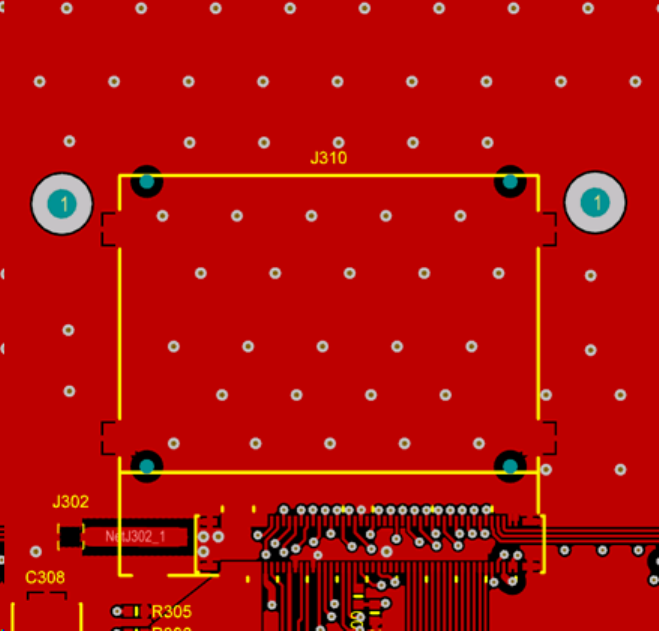
Figure: 8 - Example of good ground plane for CDMA modules
4.1.1.2 Thermal Relief
Because the ground plane acts as a large heat sink, it can affect the solderability of components. A
common method to reduce this effect is to use thermal relief around the pad in question. However, great
care must be taken when using thermal relief for high current or high frequency applications
For example, a large thermal relief like the one shown in Figure 2 can serve the purpose for general
applications such as low current, low speed data lines, DC connections and audio frequency applications.
However, such thermal relief structures should be avoided for applications where high current and/or high
frequency is involved, such as those using the cellular Module. Depending on the frequency of operation,
the long narrow thermal relief traces between the pad and the ground plane act like an RF choke. These RF
chokes become higher impedance at harmonics of the fundamental frequency making it problematic for
high frequency suppression. This can make it difficult to pass type approval testing.
- 16 -
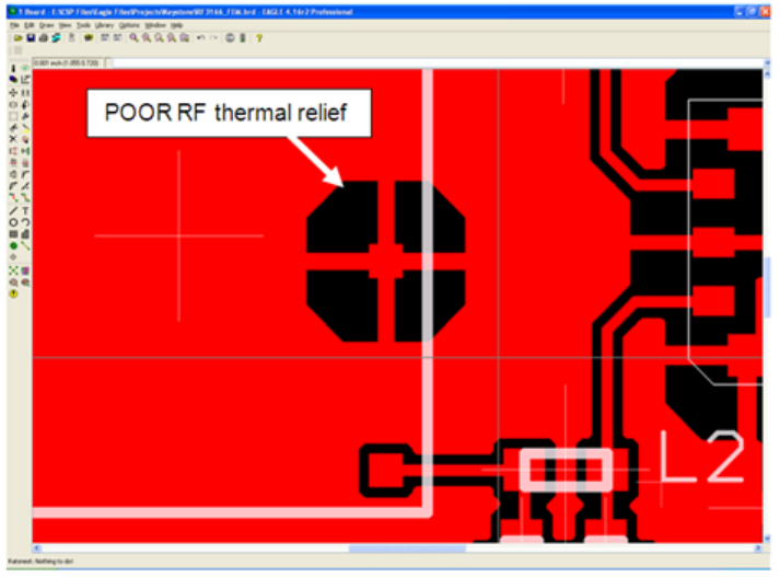
Figure: 9 - Example of a POOR RF Thermal Relief
If thermal relief is necessary, it is recommended that you use short, fat traces similar to those shown in
Figure 3. This will still provide a solderable connection, while providing a better RF connection. Making
them shorter also allows for a more continuous ground plane due to less copper being removed from the
area. It is also recommended to have ground vias around all thermal relief of critical ground pins such as
the five cellular shield tabs.
- 17 -
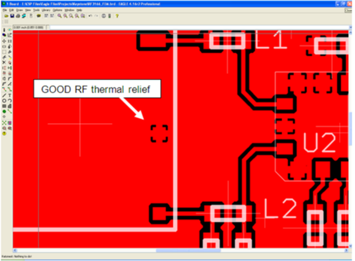
Figure: 10 - Example of a GOOD RF Thermal Relief
4.1.1.3 Antenna And RF Signal Trace
The PCB trace that feeds the RF output port must be designed for a 50 ohm characteristic impedance,
coplanar, or routed into internal layers to keep the top layer continuous around and underneath the
cellular module. Ample ground vias should be provided around the RF contacts, the RF trace and launch
pad. If possible, keep I/O and power traces away from the RF port. This includes traces running parallel or
orthogonal to it. Thermal relief should not be used on the antenna output port ground pads. The designer
must pay close attention to the size of the pad and thickness of the dielectric beneath the signal pad and
trace. Most PCB manufacturers can adjust the trace width to maintain 50 ohms impedance if the traces
are identified and instructions are included on the FAB drawing. This service is typically provided at no or
minimal additional cost.
For minimum RF emissions due to the fundamental frequency of operation, the cellular module works best
with an antenna load that has a VSWR of 1.5:1 or better. The antenna should not have gain at the harmonic
frequencies, otherwise, the conducted harmonics could get amplified to a point where the product no
longer passes type approval. However, for applications where antenna quality is less than ideal, it is
recommended to have a low pass filter (Pi structure with N=3) in the RF path to the antenna. This is a
secondary plan should there be a need to lower harmonic levels at frequencies above the PCS band. The
- 18 -
pad structure may also be used to match the antenna load impedance, if required. If it is not needed, a
capacitor of low reactance may be used to bridge the Pi structure.
The RF cable going between the cellular module and the antenna is very lossy, therefore, the length of this
cable should be kept as short a possible.
4.1.1.4 VBAT Input
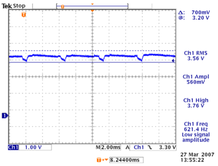
The HS 3001 Vbat input can have a relative high current draw that can fluctuate rapidly, especially when
transmitting at max power and burst mode. The Vbat interface must be designed to provide the required
instantaneous voltage and current with minimal voltage droop. This includes both sufficient bulk
decoupling capacitance as well as adequate layout provisions.
When laying out the connections to the cellular module interface connector, it is tempting to use traces of
the same width as the connector pins. However, this is a very compact connector and traces of that width
will not have sufficient copper. Similar to the discussion on thermal relief, the use of narrow traces to
connect the Vbat pins to the source voltage can act like a high impedance and cause a significant voltage
droop when higher currents are required as shown in Figure 4.
Figure: 11 - Example of Vbat Voltage Droop
- 19 -
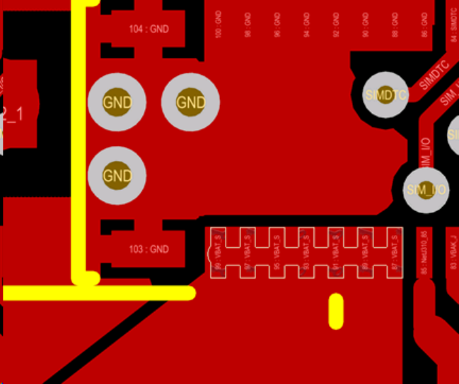
If the Vbat drops too low, the cellular modules will reset. To minimize the trace loss, it is suggested to use
a larger trace that spans several pins as shown in Figure 5. Any concern about solderability can be
mitigated by using solder mask with cutouts for the individual pins as shown by the blue lines in the figure.
The layout should provide sufficient trace width over the entire trace from the Enable modules all the way
to the source of the Vbat voltage. Any transitions between layers for this trace should utilize multiple vias.
Since even the best layout will have some impedance from the source to the cellular module, sufficient
bulk decoupling capacitance is required at the Vbat input to the cellular module. It is suggested to use at
least two 1000 uF, low ESR, tantalum capacitors located very close to the cellular interface connector Vbat
pins. Any thermal relief used on these capacitors should comply with the information given above in order
to provide the lowest impedance possible. The grounding of these capacitors is critical. Therefore, it should
be a low impedance and should utilize multiple vias to the internal ground plane close to the capacitor as
well.
Figure: 12 - Example of GOOD Vbat layout
4.1.2 Audio Reference Design
The audio quality is very dependent on the circuit design and layout. As an aid to obtaining good audio
quality, a reference design has been included below.
- 20 -
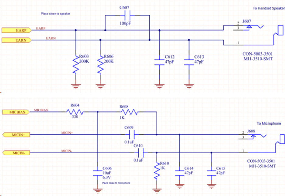
4.1.2.1 Audio Schematics
- 21 -
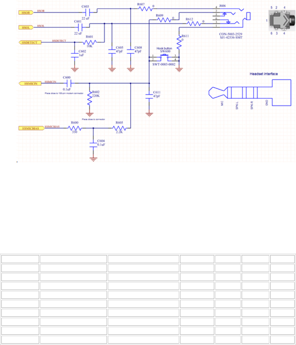
Figure: 13 - Audio Reference Design Schematic
4.2 Control Connector Signal Descriptions And Functions
Unless otherwise noted in the following sections, all digital signals will reference the following
specifications:
Parameter Parameter/Conditions Comments MIN TYP MAX UNIT
VIH High level Input voltage 1.17 1.83 V
VIL Low level Input voltage -0.3 0.63 V
Vshys Schmitt hysteresis voltage 15 mV
ILInput leakage current VDDX = Max, VIN - 0 V to VDDM 200 nA
VOH High level output voltage I out = I OH 1.35 1.8 V
VOL Low leveloutput voltage I Out = I OL 0 0.45 V
IOH High level output voltage 3 mA
IOL Low level output voltage CMOS, at pin rated drive strength 3 mA
CIN Input Capacitance 5 pF
- 22 -
4.2.1 Module Power (PINS 87, 89, 91, 93, 95, 97, 99)
The HS 3001 module uses a single voltage source of VCC=+3.3V to 4.4V.
VBAT Parameter/Conditions Min Typ Max Units
Main Battery Supply Voltage In Regulation 3.3 4.4 Vdc
Peak Current 1000 µF on Host at Module Connector 550 mA
Warning: The uplink burst will cause strong ripple on the voltage lines and should be
effectively filtered. It is recommended that 1000 µF of capacitance be placed as close
to the modem I/O connector as possible. It should be noted that the input voltage
level should not drop below the minimum voltage rating under any circumstances,
especially during the uplink burst period.
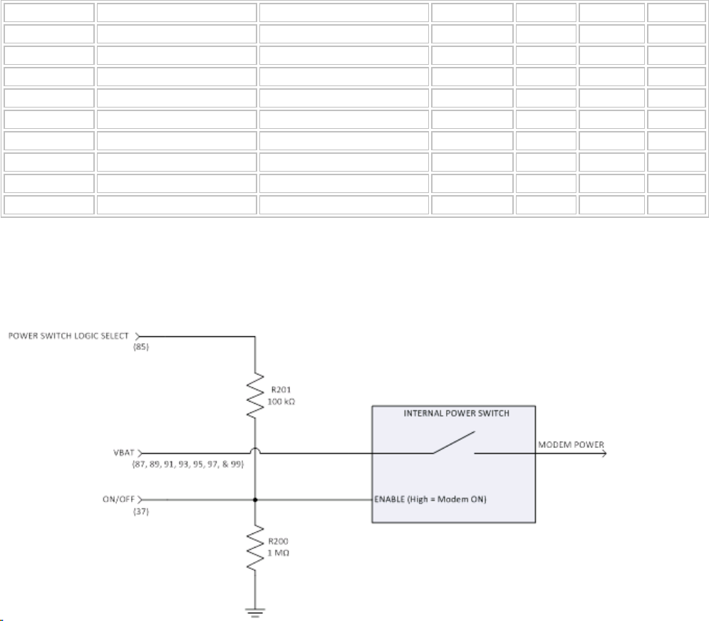
4.2.2 Modem Power-on And Recovery Techniques
The HS 3001 provides module integrators with improved modem power-on and recovery techniques, while
maintaining backwards compatibility to Enabler IIIG integrations. The addition of an internal power switch
and input power-on logic select pin, allows users the flexibility to maintain backwards compatibility or
select different power-on options. This internal power switch also allows integrators the flexibility of not
supplying an external power switch. Pin-37, previously a reset pin, has been replaced with a device power
ON/OFF pin. This pin controls the internal power switch.
Pin-85 (PSLOGIC) allows users to select the default behavior of the ON/OFF control (Pin-37). Once power is
applied via the internal power switch, Pin-35 (PHON) is used as like a phone on/off switch.
4.2.3 Power Switch Logic Detect (Pin 85)
Hardware input pin to determine the functionality of the ON/OFF pin (Pin-37). If Pin-85 is tied to VBAT,
Modem ON/OFF (Pin-37) defaults to high when open circuit, and the modem power switch will be ON. If
Pin-85 is left open, Modem ON/OFF (Pin-37) defaults to low when open circuit and the modem will be off
(requires ON/OFF to be driven high to power on).
- 23 -
Note: Externally connecting Pin-85 to ground is not recommended
4.2.4 ON/OFF (PIN 37)
Pin-37 is the ON/OFF control input for the modem's internal power switch. When it is high, the modem's
power switch will be ON. When it is low, the modem power will be OFF.
Note that Pin-35 PHON (Power On) is a signal input and is the normal method for
turning the modem ON or OFF. However, Pin 35 cannot turn the modem on if Pin 37
is low, because the modem will not have power applied to it.
Symbol Parameter Condition Min Typ Max Units
VEN_TH Enable Threshold Voltage VIN - 1.75 to 4.5V, ID = -250uA 0.4 1.25 V
IEN Enable Input Current VIN = VEN = 5.5V, ID = OPEN 2.5 4 uA
Pulldown approximately 1M ohm.
- 24 -

NOTE: The modem may not completely shut down/reset even with a mechanical
power switch or this circuit implemented if the modem’s I/O lines have another
source of power that applies voltage to the modem.
To alleviate this situation, make sure that the interface circuitry is set to tri-state or
as an input. If this is not possible, additional hardware may be needed to shunt high
impedance lines to ground during these situations.
The un-switched power source must be capable of supporting the inrush current
required by the bulk capacitance. The enable switch can be soft started via voltage
ramp or modulation to reduce the peak current as needed.
DO NOT USE a Modem Power Switch as a routine shutdown or reset. This technique
for shutting down the modem does not properly deregister the modem from the
network. The carrier may impose penalties if a fleet of equipment does not routinely
follow a proper deregistration process. If integrators wish to use this method
routinely, than a graceful detach from the network should be accomplished first. This
can be done by sending AT$OFF.
4.2.5 Phone On - PHON (PIN 35)
This input signals the modem to start and is equivalent to a “phone power button”.
A falling-edge on this Active-Low input will switch-ON the module or switch-OFF the module. The firmware
controlled OFF function will deregister the modem from the network before shutting the modem OFF.
This input has a “weak pull-up” resistor internal to the module. If users want the modem to automatically
come on when power is applied, they can tie this line low.
If RTC Sleep is required, then the PHON line must be floated to allow the internal resistor to pull the line
high. (The RTC sleep function is not available in the initial firmware release.)
Controlling the PHON signal must only be performed by an open collector/open drain device. If controlling
this signal from a microprocessor’s I/O pin, the PHON can be pulled low when the I/O is configured to be
an output and floated high by reconfiguring the pin to be an input.
Warning: The OFF Delay is controlled by the AT$OFFDLY command. A value of 0
disables the PHON line from turning the module off. 0 is the default value.
To enable the module to switch-OFF via PHON you must set AT$OFFDLY to a value
other than 0. The valid range is 100 to 1000 milliseconds.
- 25 -
Parameter Parameter/Conditions Comments MIN TYP MAX UNIT
VIH High level Input voltage 1.17 1.83 V
VIL Low level Input voltage -0.3 0.63 V
Vshys Schmitt hysteresis voltage 15 mV
ILInput leakage current VDDX = Max, VIN - 0 V to VDDM 200 nA
VOH High level output voltage I out = I OH 1.35 1.8 V
VOL Low leveloutput voltage I Out = I OL 0 0.45 V
IOH High level output voltage 3 mA
IOL Low level output voltage CMOS, at pin rated drive strength 3 mA
CIN Input Capacitance 5 pF
4.2.6 Internal Power Switch
The modem has an internal power switch that supplies the modem operating power when ON.
Figure: 14 - Internal Power Switch
4.2.7 Voltage Reference - VRIO_MSME1.8 (PIN 77)
To be used as a voltage reference source ONLY. Do not connect current loads to this pin. This pin must be
decoupled to ground with at least a 0.1 µF capacitor at the output. Noise induced on this pin will affect the
performance of the baseband.
- 26 -
4.2.8 USB (PINS 1, 3, 5, 7)
5V Tolerant Transceiver
USB Parameter/Conditions Min Typ Max Units
Input Voltage 4.4 4.65 5.25 V
Output voltage High (Driven) 2.8 3.3 3.6 Vdc
Low 0.0 0.1 0.3 Vdc
Transceiver D+/- Leakage Current -2 2 μA
4.2.9 General Purpose Input/Output Interface
GPIO number Pin number
GPIO 1 64
GPIO 2 62
GPIO 3 60
GPIO 4 58
GPIO 5 68
GPIO 6 70
GPIO 7 66
GPIO 8 72
Each general-purpose signal may be selected as inputs or outputs. The GPIOs can be used independently as
a user-specified function.
Digital I/O Specifications -Baseband Functions
Parameter Comments Min Typ Max Units
VIH High level input voltage CMOS / Schmitt 1.17 1.83 V
VIL low level input voltage CMOS / Schmitt -0.3 0.63 V
VSHYS Schmitt hysteresis voltage 100 mV
IIH Input high leakage current 1 2 No pull-down 1 uA
IIL Input high leakage current 1 2 no pull-up -1 uA
IIHPD Input high leakage current 1 with pull-down 3 30 uA
IILPU Input high leakage current 2 with pull-up -30 -3 uA
VOH High level votage CMOS, at pin rated drive strength 1.35 1.80 V
VOL Low level votage CMOS, at pin rated drive strength 0 0.45 V
IOZH 3 State leakage current 2 Logic high output 1 uA
IOZL 3 State leakage current 2 Logic low output -1 uA
- 27 -
IOZHPD 3 State leakage current 2 Logic high output with oull down 3 30 uA
IOZLPU 3 State leakage current 2 Logic high output with pull-up -30 -3 uA
IOZHKP 3 State leakage current 2 Logic high output with keeper -20 -3 uA
IOZLKP 3 State leakage current 2 Logic high output with keeper 3 20 uA
CIN Input Capacitance 7 pF
4.2.10 RTC Sleep
In this mode, the modem is off except for its Real-Time-Clock. When put into this mode, the modem can
wake itself up at a designated time/interval. See the HS 3001 AT command manual for details
4.2.11 Serial Interfaces And Handshake (Pins 11, 13, 15, 21)
The pin naming for TX/RX/RTS/CTS is referenced as a DTE .The DTE device should match their input pins to
the Enfora outputs and vice-versa. Additionally, there are AT commands that may need to be executed in
order to insure proper operation. See the chart below.
9 way D Connector Pin Number Signal Signal Direction Enfora Pin Number Enfora AT Command
2 Receive Data (RD) from DCE 15
3 Transmit Data (TD) from DTE 21
5 Signal Ground both
7 Request To Send (RTS) from DTE 11 AT+IFC
8 Clear To Send (CTS) from DCE 13 AT+IFC
Factory Set Pin Configuration
The key features of the UART in the modem mode are as follows:
l16C750 compatibility
lBaud rates: 300,600,1200,2400,4800,9600,19200,38400,57600,115200,230400
lSupported data format:
lData bit: 8 bits
lParity bit: none
lStop bit: 1 bit
lHardware flow control RTS/CTS
The HS 3001 module is designed to be used like a DTE device.
Default settings are 8 data, 1 stop, no parity, and 115200. RTS and CTS may be used for hardware
handshaking. The serial interface is 1.8V logic. By default, hardware handshaking (AT+IFC) is enabled. The
- 28 -
module will be expecting the RTS line to be low before it will transmit data. If the integrator does not wish
to use flow control, please see below for minimal serial implementations:
For a minimal Serial implementation use one of the following two configurations:
lConnect RxData (pin 15) and TxData (pin 21) to the COM port serial data lines.
lRTS (pin 11) be pulled up through a 100K resistor if not used.
lThe user must set AT+IFC=0,0 to disable flow control to communicate with the modem.
lTie RTS (pin 11) to CTS (pin 13), on the modem to loopback the flow control signals
Notes:
lTying RTS (pin 11) to ground to “spoof” flow control will cause the modem to draw more current.
lIt is not recommended to leave RTS (pin 11) unconnected.
4.2.12 Digital Audio Interface (PINS 12, 14, 16, 18)
This port is only available in Master mode and to be used for PCM digital audio. Below are the settings for
configuring its operation and the interface specification:
4.2.12.1 Digital Audio Configuration
The default settings for the digital audio are:
lMode = Master
lMCSI_CLK = 2.048MHz
lWord Size = 16 Bits
lSync Pulse = 8KHz
lFrame mode = burst
lClock edge Sync = rising edge
The following command is required to set the unit up in digital audio mode:
AT$voicepth=2
This configures the EIII module to use digital audio instead of analog audio.
4.2.12.2 Digital Audio Data Format
The 16 bit word is sent MSB first. Data received is also MSB first. No other data manipulation is done
within the module.
- 29 -
Pin Name Pin Number Signal Direction Description
PCM_RX 12 I Serial Data Input
PCM_TX 18 O Serial Data Output
PCM_CLK 14 IO Serial Clock I/O
PCM_FSYNC 16 IO Frame Synchronization I/O
4.2.13 32 KHZ Output (PIN 56)
A 32.768 kHz signal is available as an output from the module. This signal should only be used as an input
to a high impedance device. Additional loads or capacitance on the line may cause performance issues
with the module. If the line is not used, leave floating.
Parameter Comments Min Typ Max Units
Oscillation frequency 32.765 KHz
Duty Cycle 45 50 55 %
Jitter
Cycle to cycle 50 ns
period 10 ns
4.2.14 Analog-to-Digital Inputs (PIN 44 And 74)
The monitoring ADC (MADC) consists of a successive approximation 10–bit analog–to–digital converter
(ADC).
HKADC Specifications
Parameter Min Typ Max Units Comments
Resolution 12 Programmable to 8-bit or 10-bit
DNL -1 +3 LSB
INL -6 +6 LSB For V ref = VDD and 1.2 V (provided exter-
nally through AIN0)
Full scale error -25.6 +25.6 LSB ± *2.5% for V ref = VDD and 1.2 V
Offset error -12 +12 LSB for V ref = VDD and 1.2 V
Number of input
channels
5
Full scale input
range
GND VDDA V
Input resistance 1.5 KΩ S/H resistance
Input capac-
itance
12.4 pF S/H capacitor
- 30 -
Sampling time 9.6 µs
Conversion Clock 0.6 2.4 MHz 1.2 and 4.8 MHz also software pro-
grammable
Throughput rate 40.98 87.56 KHz
VDDA 2.0 2.1 2.2 V Analog power supply
VDD_MSM 1.62 1.8 1.98 V Digital power supply
VDD Operating
Current
0.5 mA
VDD_MSM Oper-
ating current
0.5 mA
Powerdown cur-
rent
1.0 µA
4.2.15 Handset Microphone Input (PINS 65, 67)
Parameter Test Conditions Min Typ Max Units Notes
Full scale input voltage voltage across either MIC 1P and MICiN, MIC2P and MIC2N 0.89 1.00 1.12 Vrms ± 1dB level error
Input impendence Difference input impedance 16 20 24 KΩ
Input impendence Single ended input impedance 8 10 12 KΩ
Input offset voltage 5 5 mV
Input capacitance At each pin of all inputs 5 pF
4.2.16 Handset Microphone BIASOutput (PIN 63)
Parameter Comments Min Typ Max Units
MIC bias output voltage 1.8 V
MIC bias output current 1.5 mA
MIC bias voltage accuracy Minimum load -3 +3 %
MIC bias output voltage load regulation 30 Ω
Supply current
Active State 50 100 uA
Idle State 10 100 uA
4.2.17 Handset Speaker Output (PINS 71, 73)
Parameter Test Conditions Min Typ Max Units Notes
DAC to
EAROP/EARON
fullscale output
f = 1.02 Hz, 0 dBFs 1.11 1.25 1.40 Vrms ± 1 dB level error
EAROP/EARON f = 498 Hz, 0 dBFs 38.5 48.8 61.3 mW 22 to 20 kHz
- 31 -
output power,
4% or less THD+N
measurement
BW
Output DC level,
EAR1OP and
EAR1ON with
respect to VSS
Input = .999 dBFs 1.03 1.05 1.07 V
4.2.18 Headset Microphone Input (PIN 55)
Parameter Test Conditions Min Typ Max Units Notes
Full scale input voltage voltage across oin 55 and ground 0.89 1.00 1.12 Vrms ± 1dB level error
Input impendence Single ended input impedance 8 10 12 KΩ
Input offset voltage 5 5 mV
Input capacitance At each pin of all inputs 5 pF
4.2.19 Headset Speaker Output Left And Right (PINS 57, 59)
Parameter Test Conditions Min Typ Max Units Notes
Both modes - HPH_LP and HPH_RN configured single ended, analog volume control = 0 dB
DAC to HPH_LP and HPH_RN
fullscale output
f = 1.02 kHz, 0 bDFS 0.531 0.595 0.668 Vrms
Output DC level, HPH_LP and
HRH_RN wih respect to VSS
Input = 0.999 dBFs 1.03 1.05 1.07 V
Output impedence 0.5 Ω
Voice Mode - HPH_LP and / or HPH_RN configured single ended, analog volume control =0 dB
HPH_LP and HPH_RN output
power, 4% or less THD+N
f = 1.02 kHz, 0 bDFS 17.6 22.1 27.9 mW 22 to 20 kHz
measurement
bandwidth
DAC to HPH_LP and HPH_RN
output noise level
Input = 0.999 dBFs, Fs = 8 kHz or 16
kHz, A-weighted
106 uVrms
Both modes - HPH_LP and HPH_RN configureddifferential (HPH_LP/HPH_RN), analog volume control = 0 dB
DAC to HPH_LP and HPH_RN
fullscale output
f = 1.02 kHz, 0 dBFS, 32Ω load 1.06 1.19 1.34 Vrms
DAC to HPH_LP/HPH_RN gain
error relative to gain @ -3 dBFS
f = 1.02 kHz, -60 dBFS -1.2 1.2 dB Linearty spot
check
Output DC level, HPH_P and
HPH_N with respect to VSS
Input = .999 dBFs 1.03 1.05 1.07 V
Output impedence 1.0 Ω
Voice Mode - HPH_LP and / or HPH_RN configured differential (HPH_LP/HPH_RN), analog volume control =0 dB
HPH_LP/HPH_RN output
power, 4% or less THD+N
f = 498 Hz, -3 dBFS, 32Ω 17.6 22.1 27.9 mW 22 to 20 kHz
measurement
bandwidth
DAC to HPH_LP/HPH_RN out- Input = 0.999 dBFS, Fs = 8 kHz, A- 212 uVrms 22 to 20 kHz
- 32 -
put noise level weighted measurement
bandwidth
4.2.20 Headset Detect (PIN 47)
Parameter Parameter/Conditions Comments MIN TYP MAX UNIT
VIH High level Input voltage 1.17 1.83 V
VIL Low level Input voltage -0.3 0.63 V
Vshys Schmitt hysteresis voltage 15 mV
ILInput leakage current VDDX = Max, VIN - 0 V to VDDM 200 nA
VOH High level output voltage I out = I OH 1.35 1.8 V
VOL Low leveloutput voltage I Out = I OL 0 0.45 V
IOH High level output voltage 3 mA
IOL Low level output voltage CMOS, at pin rated drive strength 3 mA
CIN Input Capacitance 5 pF
4.3 Circuit Protection
Other than very low level ESD protection within the module’s integrated circuits, the module does not have
any protection against ESD events or other excursions that exceed the specified operating parameters.
Generally, ESD protection (typically TVS/Transzorb devices) should be added to all signals that leave the
host board. This includes VBAT/VCC.
Series resistors (typically 47 ohm) can also be added in series with data lines to limit the peak current
during a voltage excursion.
Warning: It is the Integrator’s responsibility to protect the Enabler module from
electrical disturbances and excursions, which exceed the specified operating
parameters.
- 33 -