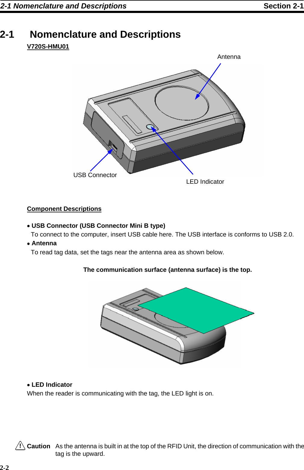
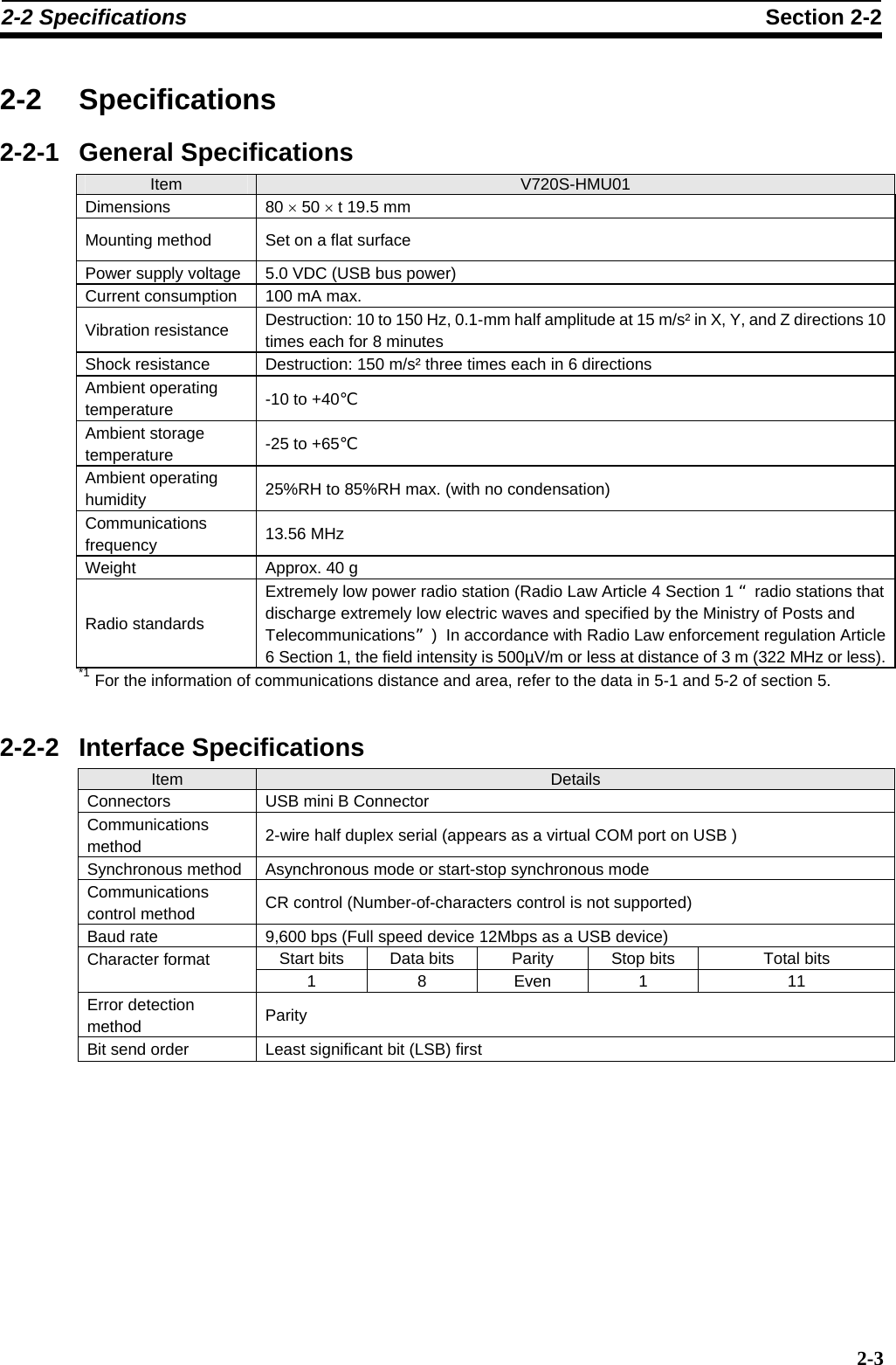
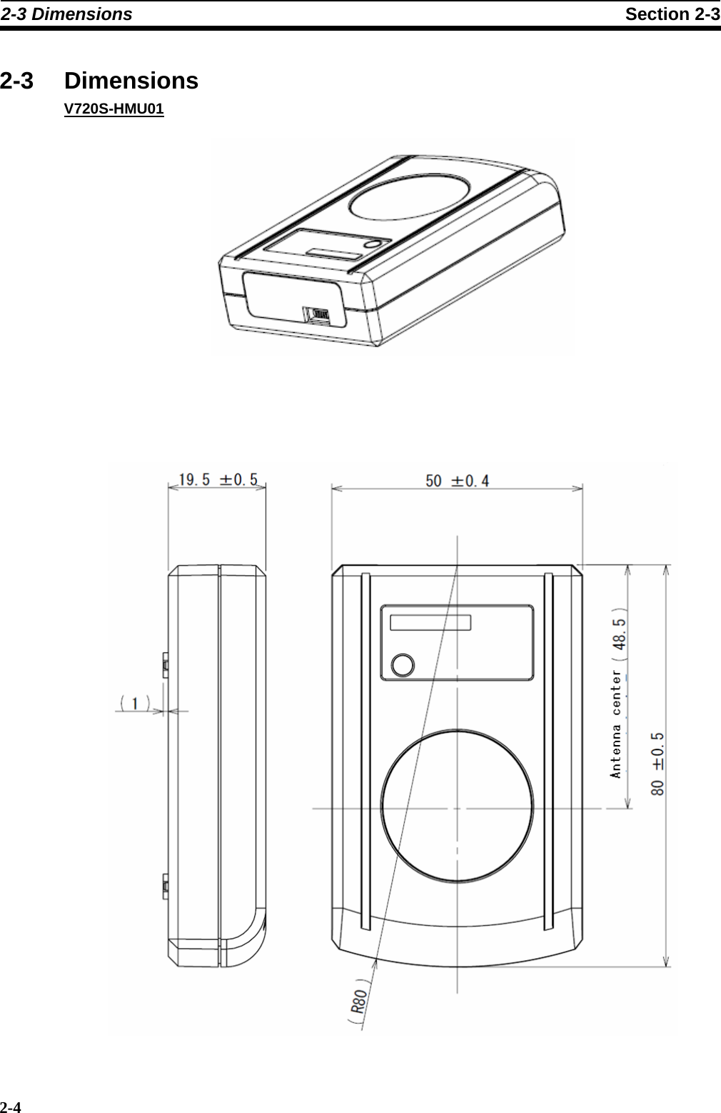
Omron RFID Business Development Department V720SHMU01 RFID Transmitter User Manual
Omron Corporation, RFID Business Development Department RFID Transmitter
UserManual.wiki
>
Omron RFID Business Development Department
>
V720SHMU01 User Manual
user manual
Navigation menu
Upload a User Manual
Namespaces
Wiki Guide
HTML
PDF
Info
Views
User Manual
Discussion / Help
Navigation


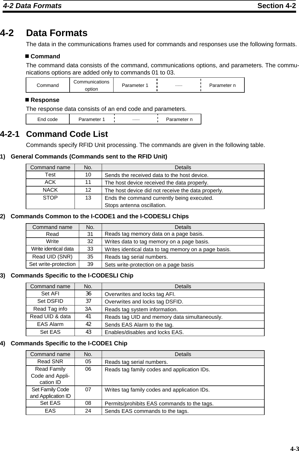

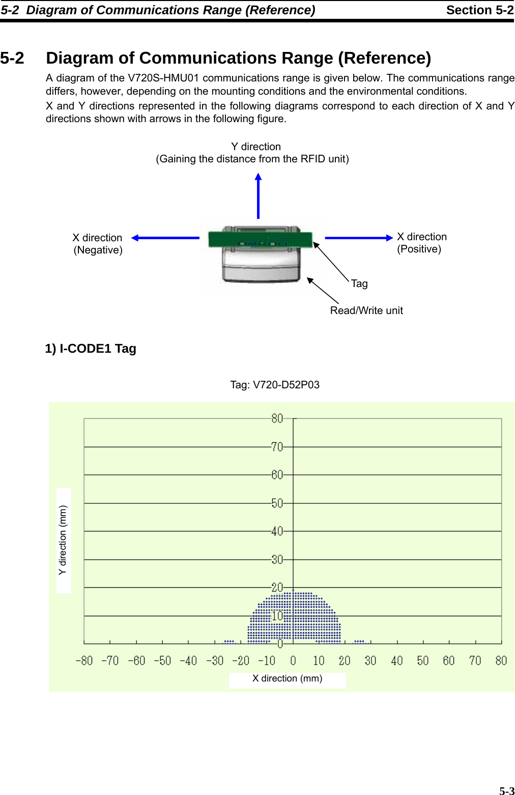
![5-3 Communications Time (Reference) Section 5-3 5-8 Example: Reading data from pages 1, 5, and 9 T = 1.3 × ( 9 - 1 + 1 ) + 6.2 = 17.9 ms (for I-CODE1) T = 1.3 × (9 - 1 + 1 ) + 6.0 = 17.7 ms (for I-CODESLI) Example: Reading data from pages C, 5, and 9 T = 1.3 × (9-(-4)+1) + 6.2 = 24.4ms (for I-CODE1) T = 1.3 × (12-5+1) + 6.0 = 16.6ms (for I-CODESLI) Example: Writing data to pages 2, 4, 9, and 10 T = 11.7 × 4 + 1.3 × ( 10 - 2 + 1 ) + 13.5 = 72ms (for I-CODE1) T = 12.3 × 4 + 1.3 × ( 10 - 2 + 1 ) + 15.5 = 76.4ms (for I-CODESLI) Communications Time Calculation Conditions • Communications mode: Single Trigger Mode • Communications errors must not occur, such as due to noises. 5-3-2 TAT (Turn Around Time) The TAT is the time taken from when the host control unit sends a command to the RFID Unit, to when a response is received and completed. The time differs depending on the baud rate and the communications control method setting. Example of TAT Calculation Example: Reading from page 0 to page 4 I-CODE1 I-CODESLI (1)During command send 9[char.] × 11 [bits] / 9600[bps] × 1000[ms/s] ≈ 10.32ms (2)During communications 6.5 + 6.2 = 12.7ms (3)During reception of response 43[char.] × 11 [bits] / 9600[bps] × 1000[ms/s] ≈ 49.27ms The TAT in to the above example is (1) + (2) + (3) = 72.29 ms. (1)During command send 11[char.] × 11 [bits] / 9600[bps] × 1000[ms/s] ≈ 12.61ms (2)During communications 6.5 + 6.0 = 12.5ms (3)During reception of response 43[char.] × 11 [bits] / 9600[bps] × 1000[ms/s] ≈ 49.27ms The TAT in to the above example is (1) + (2) + (3) = 74.38 ms. The calculations are performed according to the following conditions. • Communications mode : Single Trigger Mode • Communications control method : CR control • Baud rate : 9,600 bps • Data code specification : Hexadecimal • Commands sent from the host control unit are sent continuously without spaces between the characters. • Communications errors must not occur, such as due to noises.](https://usermanual.wiki/Omron-RFID-Business-Development-Department/V720SHMU01/User-Guide-887058-Page-55.png)
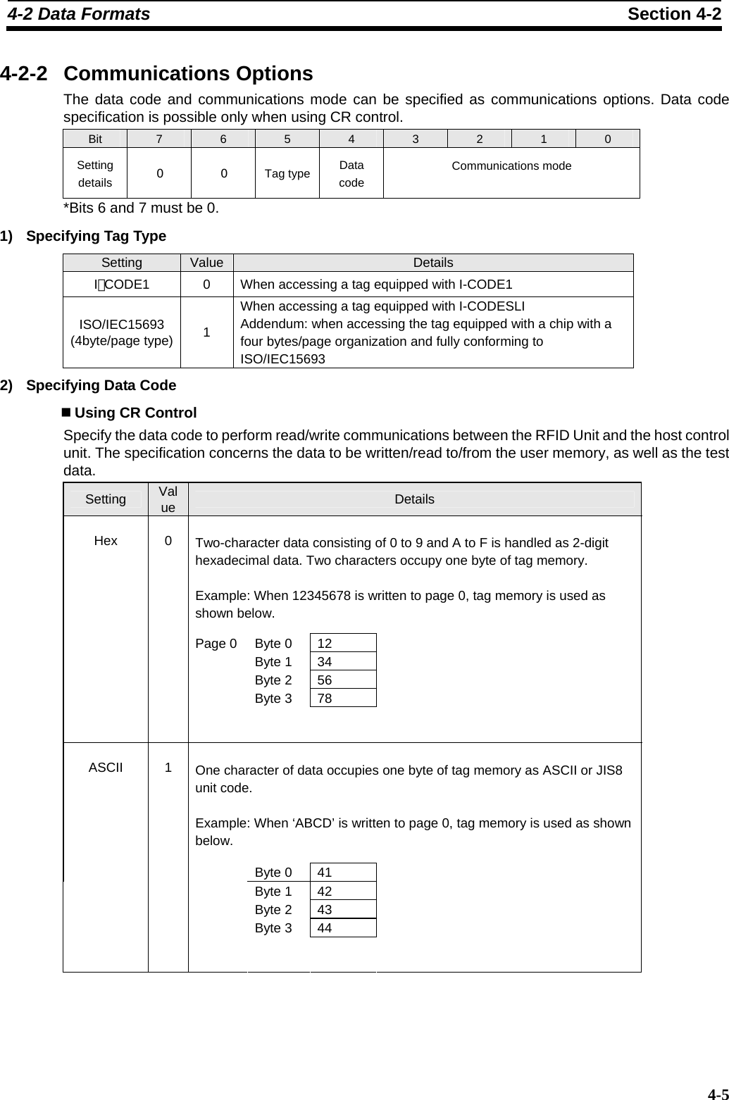
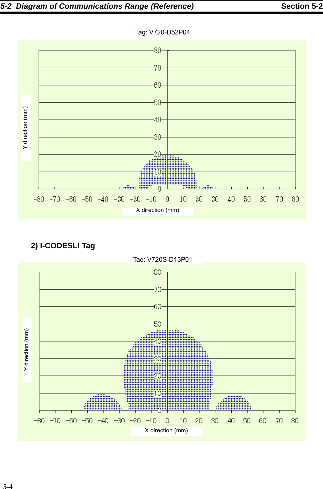
![6-1 Before Installation 6-1 6-2 6-1 Before Installation This section describes how to install the specified device driver (called “Driver”), which has to be installed in the computer to operate the RFID unit (V720S-HMU01). This Driver appears as a virtual COM port on the computer. [System Requirements] Make sure the computer to be connected with the RFID unit meets the system requirements for running the Driver as below. ●OS: Windows XP home/Professional or Windows 2000 Professional. ●USB port available (USB1.0 or USB2.0) ●The specified Driver installable. ●An administrator of the computer shall install the Driver. [How to obtain the Driver] Visit our Web site (http://www.omronrfid.com/) and download the Driver from the download page. If you download the Driver, the compressed file of V720S-HMU01.exe is stored in the computer. Note: - The Driver must be installed before connecting the RFID unit to your computer. - If you happen to connect the RFID unit to the computer before installation of the Driver, cancel the connection then start to install referring to “If you connect before installing” described in the end of this section. - An administrator of the computer shall install the Driver. 6-2 Driver Installation [Decompression of the Driver] (1) Run the V720S-HMU01(E).exe downloaded from the Web site mentioned above. (2) The following dialog appears.](https://usermanual.wiki/Omron-RFID-Business-Development-Department/V720SHMU01/User-Guide-887058-Page-60.png)
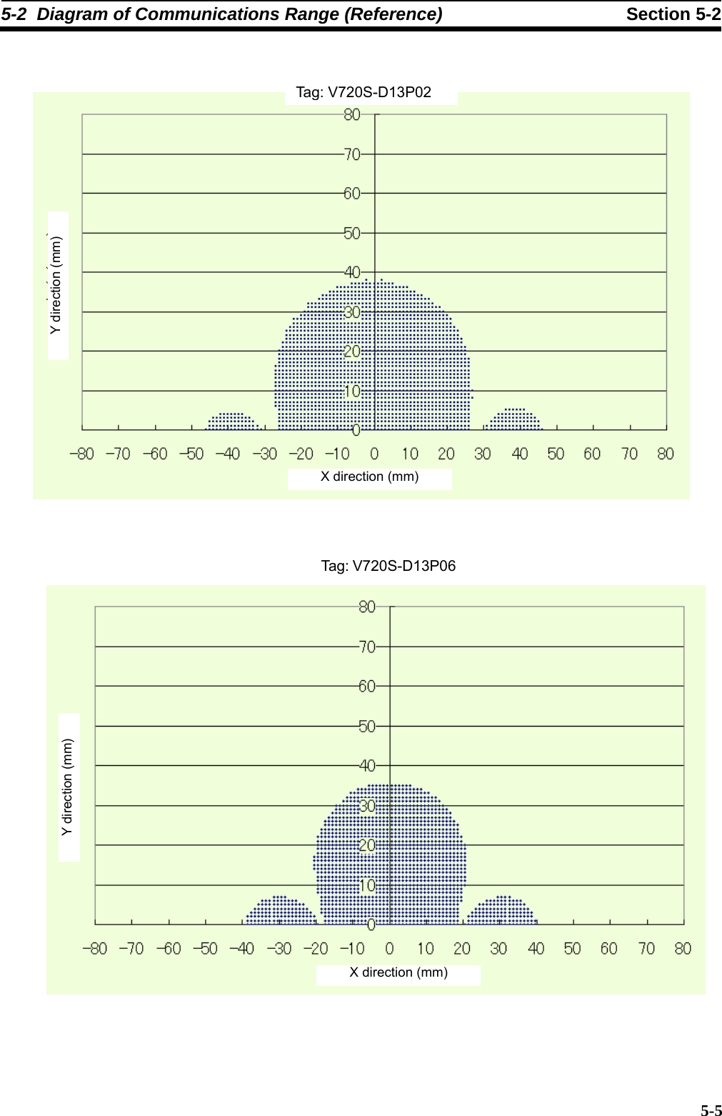
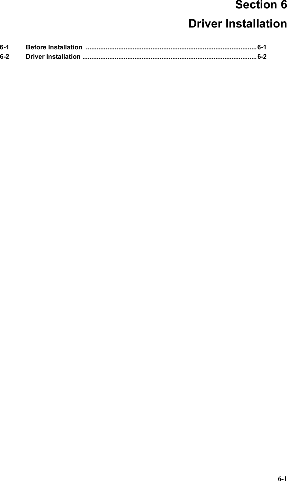
![6-2 Driver Installation 6-2 6-3 (3) If you change the direction of the decompressed file, click “Change” then click “OK”. If you do not change the direction, just click “OK”. (4) The folder V720S-HMU01 appears in the directed folder. If you do not change the direction, the folder V720S-HMU01 appears in the same folder as V720S-HMU01.exe is placed. V720S-HMU01 folder includes following two folders, driver <= In this folder, the Driver is stored. utility <= Utilities to be used for identification of port numbers are stored. [Driver Installation] (1) Double click the setup.exe in the driver folder to start the installation process. (2) When the Install Driver dialog appears, click “Install”. z If you use Windows XP SP2 or later version, the following page appears. On this page, click “Continue” to go back to the Install Driver page. This warning page appears twice. On each page, click “Continue”. z If you use Windows 2000, this page does not appear. (3) Install Driver page appears again and installation is processed. Then, on the setup page, click OK to complete the install process.](https://usermanual.wiki/Omron-RFID-Business-Development-Department/V720SHMU01/User-Guide-887058-Page-61.png)
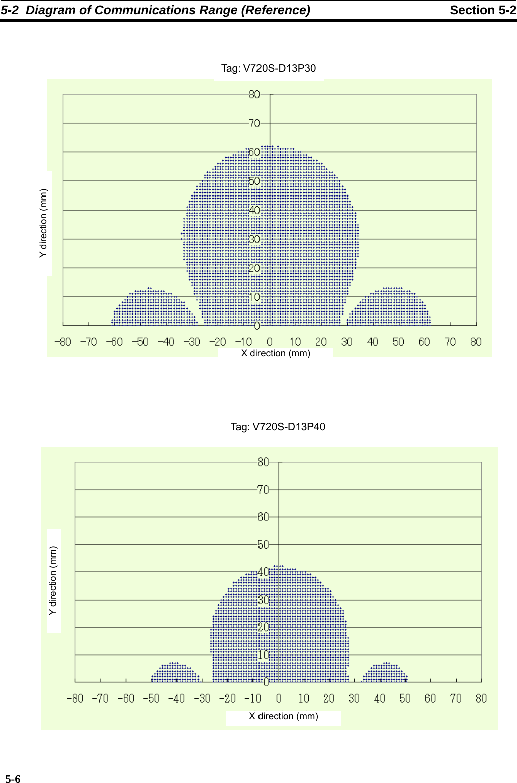
![6-2 Driver Installation 6-2 6-4 [Connection with RFID Unit] After installing the Driver, connect the RFID unit (V720S-HMU01) to the computer through USB connector. (1) Just after connecting the RFID unit to the computer, following page appears. (2) On the “Found New Hardware Wizard” page, Click “No, not this time” and then click “Next”. If you use the Windows 2000, this page is automatically skipped and the following page appears. (3) On the second “Found New Hardware Wizard” page, make sure “Install the software automatically [Recommended]” is checked then click the “Next” button.](https://usermanual.wiki/Omron-RFID-Business-Development-Department/V720SHMU01/User-Guide-887058-Page-62.png)
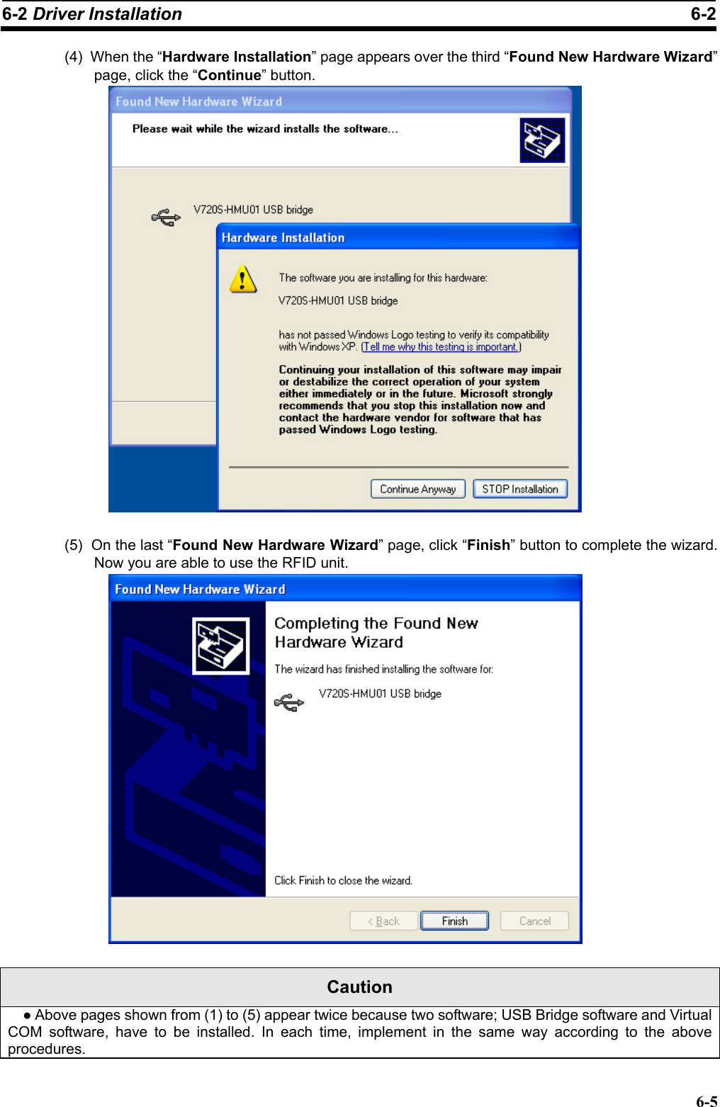
![6-2 Driver Installation 6-2 6-6 [If you connect RFID unit before installing the Driver] If you connect the RFID unit to the computer before installing the Driver, you can not set up the Driver in the usual manner. After connecting the unit to the computer, one of following pages will appear. See which page appears on your computer window and follow the procedures corresponding to the page. (1) On the page as below, click the “Cancel” button and then remove the RFID unit. Start Driver installation according to the procedures described at the beginning of this section. (2) On the page as below, click the “Cancel” button and then remove the RFID unit. Start Driver installation according to the procedures described at the beginning of this section.](https://usermanual.wiki/Omron-RFID-Business-Development-Department/V720SHMU01/User-Guide-887058-Page-64.png)
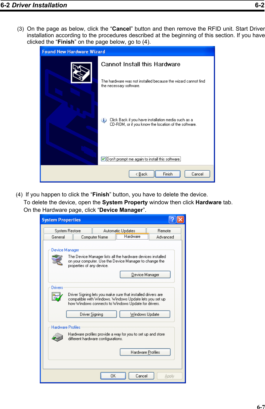
![6-2 Driver Installation 6-2 6-8 (5) On the Device Manager page, make sure OMRON V720S-HMU01 appears under the “Other Device”. (6) Point the OMRON V720S-HMU01 and click the right mouse button to open drop-down menu. Choose the “Delete” in the menu to complete deletion. After deleting the device, remove the RFID unit, then start to install the Driver again. [To See Port Number] Find the disPort.exe file in the utility folder that is extracted from the driver file, V720S-HMU01.exe. Click the disPort.exe file. Following dialogue appears. You can check what port number is assigned for the RFID unit (In the case of above dialogue, COM3: is assigned.) Caution ● Execution of dispPort.exe requires another file CP210xManufacturing.dll in the same folder. If you copy or move the dispPort.exe to use it, copy or move the CP210xManufacturing.dll file into the same place.](https://usermanual.wiki/Omron-RFID-Business-Development-Department/V720SHMU01/User-Guide-887058-Page-66.png)